US8868952B2 - Controller and program product - Google Patents
Controller and program product Download PDFInfo
- Publication number
- US8868952B2 US8868952B2 US13/345,824 US201213345824A US8868952B2 US 8868952 B2 US8868952 B2 US 8868952B2 US 201213345824 A US201213345824 A US 201213345824A US 8868952 B2 US8868952 B2 US 8868952B2
- Authority
- US
- United States
- Prior art keywords
- interrupt
- unit
- time
- processor
- mode
- Prior art date
- Legal status (The legal status is an assumption and is not a legal conclusion. Google has not performed a legal analysis and makes no representation as to the accuracy of the status listed.)
- Expired - Fee Related, expires
Links
Images


Classifications
-
- G—PHYSICS
- G06—COMPUTING; CALCULATING OR COUNTING
- G06F—ELECTRIC DIGITAL DATA PROCESSING
- G06F9/00—Arrangements for program control, e.g. control units
- G06F9/06—Arrangements for program control, e.g. control units using stored programs, i.e. using an internal store of processing equipment to receive or retain programs
- G06F9/46—Multiprogramming arrangements
- G06F9/48—Program initiating; Program switching, e.g. by interrupt
- G06F9/4806—Task transfer initiation or dispatching
- G06F9/4843—Task transfer initiation or dispatching by program, e.g. task dispatcher, supervisor, operating system
- G06F9/4881—Scheduling strategies for dispatcher, e.g. round robin, multi-level priority queues
- G06F9/4893—Scheduling strategies for dispatcher, e.g. round robin, multi-level priority queues taking into account power or heat criteria
-
- G—PHYSICS
- G06—COMPUTING; CALCULATING OR COUNTING
- G06F—ELECTRIC DIGITAL DATA PROCESSING
- G06F1/00—Details not covered by groups G06F3/00 - G06F13/00 and G06F21/00
- G06F1/26—Power supply means, e.g. regulation thereof
- G06F1/32—Means for saving power
- G06F1/3203—Power management, i.e. event-based initiation of a power-saving mode
- G06F1/3206—Monitoring of events, devices or parameters that trigger a change in power modality
- G06F1/3228—Monitoring task completion, e.g. by use of idle timers, stop commands or wait commands
-
- G—PHYSICS
- G06—COMPUTING; CALCULATING OR COUNTING
- G06F—ELECTRIC DIGITAL DATA PROCESSING
- G06F1/00—Details not covered by groups G06F3/00 - G06F13/00 and G06F21/00
- G06F1/26—Power supply means, e.g. regulation thereof
- G06F1/32—Means for saving power
- G06F1/3203—Power management, i.e. event-based initiation of a power-saving mode
- G06F1/3234—Power saving characterised by the action undertaken
- G06F1/324—Power saving characterised by the action undertaken by lowering clock frequency
-
- G—PHYSICS
- G06—COMPUTING; CALCULATING OR COUNTING
- G06F—ELECTRIC DIGITAL DATA PROCESSING
- G06F1/00—Details not covered by groups G06F3/00 - G06F13/00 and G06F21/00
- G06F1/26—Power supply means, e.g. regulation thereof
- G06F1/32—Means for saving power
- G06F1/3203—Power management, i.e. event-based initiation of a power-saving mode
- G06F1/3234—Power saving characterised by the action undertaken
- G06F1/3243—Power saving in microcontroller unit
-
- G—PHYSICS
- G06—COMPUTING; CALCULATING OR COUNTING
- G06F—ELECTRIC DIGITAL DATA PROCESSING
- G06F1/00—Details not covered by groups G06F3/00 - G06F13/00 and G06F21/00
- G06F1/26—Power supply means, e.g. regulation thereof
- G06F1/32—Means for saving power
- G06F1/3203—Power management, i.e. event-based initiation of a power-saving mode
- G06F1/3234—Power saving characterised by the action undertaken
- G06F1/3287—Power saving characterised by the action undertaken by switching off individual functional units in the computer system
-
- Y02B60/144—
-
- Y02B60/32—
-
- Y—GENERAL TAGGING OF NEW TECHNOLOGICAL DEVELOPMENTS; GENERAL TAGGING OF CROSS-SECTIONAL TECHNOLOGIES SPANNING OVER SEVERAL SECTIONS OF THE IPC; TECHNICAL SUBJECTS COVERED BY FORMER USPC CROSS-REFERENCE ART COLLECTIONS [XRACs] AND DIGESTS
- Y02—TECHNOLOGIES OR APPLICATIONS FOR MITIGATION OR ADAPTATION AGAINST CLIMATE CHANGE
- Y02D—CLIMATE CHANGE MITIGATION TECHNOLOGIES IN INFORMATION AND COMMUNICATION TECHNOLOGIES [ICT], I.E. INFORMATION AND COMMUNICATION TECHNOLOGIES AIMING AT THE REDUCTION OF THEIR OWN ENERGY USE
- Y02D10/00—Energy efficient computing, e.g. low power processors, power management or thermal management
-
- Y—GENERAL TAGGING OF NEW TECHNOLOGICAL DEVELOPMENTS; GENERAL TAGGING OF CROSS-SECTIONAL TECHNOLOGIES SPANNING OVER SEVERAL SECTIONS OF THE IPC; TECHNICAL SUBJECTS COVERED BY FORMER USPC CROSS-REFERENCE ART COLLECTIONS [XRACs] AND DIGESTS
- Y02—TECHNOLOGIES OR APPLICATIONS FOR MITIGATION OR ADAPTATION AGAINST CLIMATE CHANGE
- Y02D—CLIMATE CHANGE MITIGATION TECHNOLOGIES IN INFORMATION AND COMMUNICATION TECHNOLOGIES [ICT], I.E. INFORMATION AND COMMUNICATION TECHNOLOGIES AIMING AT THE REDUCTION OF THEIR OWN ENERGY USE
- Y02D30/00—Reducing energy consumption in communication networks
- Y02D30/50—Reducing energy consumption in communication networks in wire-line communication networks, e.g. low power modes or reduced link rate
Definitions
- Embodiments described herein relate generally to a controller and a program product.
- a processing device for example, a microprocessor
- a dynamic voltage frequency scaling (DVFS) technique that reduces a power supply voltage or a frequency to reduce the power consumption
- DVFS dynamic voltage frequency scaling
- a power gating technique that supplies power only to a portion requiring power.
- the power gating technique there is a technique that divides a processor into a plurality of clock domains and determines whether to supply power to each clock domain.
- a fine grain power gating technique that determines whether to supply power to each computing unit in a processor.
- FIG. 1 is a block diagram illustrating a target system according to a first embodiment
- FIG. 2 is a block diagram illustrating a processor according to the first embodiment
- FIG. 3 is a diagram illustrating an example of information stored in an operation mode storage unit
- FIG. 4 is a sequence diagram illustrating the operation of the target system according to the first embodiment
- FIG. 5 is a sequence diagram illustrating the operation of the target system according to the first embodiment
- FIG. 6 is a sequence diagram illustrating the operation of the target system according to the first embodiment
- FIG. 7 is a block diagram illustrating a target system according to a second embodiment
- FIG. 8 is a block diagram illustrating a processor according to the second embodiment
- FIG. 9 is a diagram illustrating an example of information stored in a fourth storage unit.
- FIG. 10 is a diagram illustrating an example of information stored in a fifth storage unit
- FIG. 11 is a sequence diagram illustrating the operation of the target system according to the second embodiment.
- FIG. 12 is a sequence diagram illustrating the operation of the target system according to the second embodiment.
- FIG. 13 is a sequence diagram illustrating the operation of the target system according to the second embodiment
- FIG. 14 is a sequence diagram illustrating the operation of the target system according to the second embodiment.
- FIG. 15 is a sequence diagram illustrating the operation of the target system according to the second embodiment.
- FIG. 16 is a block diagram illustrating a target system according to a third embodiment
- FIG. 17 is a sequence diagram illustrating the operation of the target system according to the third embodiment.
- FIG. 18 is a block diagram illustrating a target system according to a fourth embodiment
- FIG. 19 is a sequence diagram illustrating the operation of the target system according to the fourth embodiment.
- FIG. 20 is a block diagram illustrating a target system according to a fifth embodiment
- FIG. 21 is a sequence diagram illustrating the operation of the target system according to the fifth embodiment.
- FIG. 22 is a diagram illustrating a modification of the information stored in the operation mode storage unit
- FIG. 23 is a block diagram illustrating a target system according to a modification.
- FIG. 24 is a block diagram illustrating a target system according to a modification.
- a controller includes a state detecting unit, a calculating unit, and a determining unit.
- the state detecting unit detects an idle state in which indicates there are no processes that can execute on a processing device capable of performing one or more processes.
- the calculating unit calculates a resuming time, which indicates a time length until a next process starts, when the state detecting unit detects the idle state.
- the determining unit determines an operation mode of the processing device on the basis of the resuming time calculated by the calculating unit.
- FIG. 1 is a block diagram illustrating an example of the schematic structure of a target system according to a first embodiment.
- the target system includes a processor 100 , a resume control unit 700 , and a storage area 900 which are connected to each other by a bus 950 .
- the processor 100 is a processing device that can execute one or more processes.
- the processor 100 includes a CPU 20 and a third storage unit 110 .
- the third storage unit 110 includes a register 120 that stores various kinds of data and a cache memory 140 that stores, for example, frequently-used data.
- each of the register 120 and the cache memory 140 is a volatile memory.
- the resume control unit 700 is for resuming the operation of the processor 100 which is in a power saving state (sleep state), which will be described later.
- the resume control unit 700 includes a second storage unit 710 , a resume time setting unit 720 , and a resume unit 730 .
- the second storage unit 710 stores resuming time, indicating a time which the processor should be resumed by timer interrupt.
- the resume time setting unit 720 sets the resuming time notified by the processor 100 to the second storage unit 710 .
- the resume unit 730 resumes the operation of the processor 100 .
- the above-mentioned operation will be described in detail later.
- the storage area 900 When power is turned off and then turned on, the storage area 900 is capable of recovering internal data.
- the storage area capable of recovering internal data there is a non-volatile memory and the storage area may be a magnetic random access memory (MRAM) or a ferroelectric random access memory (FeRAM).
- MRAM magnetic random access memory
- FeRAM ferroelectric random access memory
- the storage area is not limited to the non-volatile memory.
- the storage area may be a general dynamic random access memory (DRAM) having a mechanism that recoveries internal data when power is turned on.
- DRAM general dynamic random access memory
- FIG. 2 is a block diagram illustrating the structure of functions implemented by the CPU 20 provided in the processor 100 to execute an operating system (OS) 200 , which is basic software, and hardware components of the processor 100 .
- OS operating system
- FIG. 2 represents that the processor 100 includes the hardware components, the OS 200 operated on the processor 100 , and one or more processes operated on the OS 200 .
- the hardware components of the processor 100 includes the CPU 20 , a first storage unit 210 , and an operation mode storage unit 220 .
- the first storage unit 210 stores therein timer information.
- the timer information includes set time and a process which is performed at the set time.
- the operation mode storage unit 220 stores therein the relation between resuming time, indicating a time which the processor should be resumed by timer interrupt, and the operation mode to be set. This will be described in detail later.
- the OS 200 includes a state detecting unit 230 , a calculating unit 240 , a determining unit 250 , a second mode unit 260 , a first mode unit 270 , and a restore unit 280 .
- the state detecting unit 230 can detect an idle state.
- the idle state means a state in which the processor 100 performs no process.
- the calculating unit 240 calculates the resuming time indicating a time length until the next process starts, using the timer information stored in the first storage unit 210 . Specifically, the calculating unit 240 calculates the time when the next process starts from the timer information stored in the first storage unit 210 and calculates, as the resuming time, the time length of the difference between the calculated time and the current time.
- the determining unit 250 acquires the resuming time from the calculating unit 240 and determines the operation mode of the processor 100 on the basis of the acquired resuming time. Specifically, the determining unit 250 determines the operation mode of the processor 100 on the basis of the resuming time acquired from the calculating unit 240 and the data stored in the operation mode storage unit 220 . This will be described in detail below.
- FIG. 3 is a diagram illustrating an example of information stored in the operation mode storage unit 220 . As shown in FIG. 3 , the operation mode storage unit 220 stores therein the relation between the resuming time and the operation mode to be set.
- the determining unit 250 determines the operation mode of the processor 100 to be a first mode in which the operation of the processor is temporarily stopped and the processor becomes a power saving state (sleep state). On the other hand, when the resuming time is equal to or less than t 1 , the determining unit 250 determines the operation mode of the processor 100 to be a second mode in which the processor 100 is still in the idle state.
- the second mode unit 260 performs the processor 100 is still in the idle state (referred to as an idle task).
- the determining unit 250 determines the operation mode of the processor 100 to be the first mode
- the first mode unit 270 saves the data stored in the register 120 and the cache memory 140 to the storage area 900 and temporarily stops the operation of the processor 100 such that the processor 100 becomes the power saving state (sleep state).
- the restore unit 280 restores the data saved in the storage area 900 to the register 120 , which will be described in detail later.
- FIG. 4 is a sequence diagram illustrating an example of a process from the detection of the idle state of the processor 100 to the determination of the operation mode of the processor 100 .
- the state detecting unit 230 detects the idle state of the processor 100 (Step S 400 ) and requests the determining unit 250 to determine the operation mode (Step S 401 ).
- the determining unit 250 requests the calculating unit 240 to calculate the resuming time (Step S 402 ).
- the calculating unit 240 reads the timer information stored in the first storage unit 210 (Step S 403 ). Then, the calculating unit 240 extracts the time when the next process is performed from the read timer information and calculates, as the resuming time, the time length of the difference between the extracted time and the current time (Step S 404 ). Then, the calculating unit 240 notifies the calculated resuming time to the determining unit 250 (Step S 405 ).
- the determining unit 250 determines the operation mode on the basis of the resuming time acquired from the calculating unit 240 and the data stored in the operation mode storage unit 220 (Step S 406 ).
- FIG. 5 is a sequence diagram illustrating an example of a process until the processor 100 becomes the sleep state after the operation mode of the processor 100 is determined to be the first mode.
- the determining unit 250 requests the first mode unit 270 to temporarily stop the operation of the processor 100 (Step S 501 ).
- the determining unit 250 requests to temporarily stop the operation of the processor 100 and notifies the resuming time acquired from the calculating unit 240 to the first mode unit 270 .
- the first mode unit 270 notifies the resuming time notified by the determining unit 250 to the resume time setting unit 720 (Step S 502 ). Then, the resume time setting unit 720 registers the resuming time notified by the first mode unit 270 to the second storage unit 710 (Step S 503 ). Then, the resume time setting unit 720 notifies the first mode unit 270 that the registration of the resuming time has been completed (Step S 504 ).
- the first mode unit 270 flushes the data stored in the cache memory 140 to the storage area 900 (Step S 505 ).
- the flushed (transmitted) data is written to the storage area 900 .
- the first mode unit 270 saves the data stored in the register 120 to the storage area 900 (Step S 506 ).
- the first mode unit 270 temporarily stops the operation of the processor 100 and shifts the state of the processor 100 to the power saving state (sleep state) (Step S 507 ).
- FIG. 6 is a sequence diagram illustrating an example of a process until the time reaches the resume time and the operation of the processor 100 resumes. As shown in FIG. 6 , when it is detected that the time reaches the resume time (Step S 600 ), the resume unit 730 resumes the operation of the processor 100 to cancel the first mode (Step S 601 ).
- the restore unit 280 restores the data which is saved to the storage area 900 by the first mode unit 270 to the register 120 (Step S 602 ). Then, the process proceeds to a step which will be performed at the resume time (Step S 603 ).
- the operation mode of the processor 100 is determined on the basis of the resuming time calculated from the timer information. Specifically, when the resuming time is more than a predetermined time length (t 1 ), the processor 100 becomes the sleep state. When the resuming time is equal to or less than the predetermined time length, the processor 100 is maintained in the idle state. Therefore, it is possible to effectively reduce the power consumption of the processor 100 .
- a method of shifting the processor 100 to the sleep state to reduce the power consumption can reduce the power consumption of the processor 100 .
- a large overhead occurs due to, for example, a process for temporarily stopping the operation of the processor 100 and power consumption caused by the process (for example, the saving or restoring of data to the register and the flushing of data in the cache memory) or the influence of the process (for example, an increase in the number of memory accesses due to the flushing of data in the cache memory) is not negligible.
- power consumption when the processor 100 is shifted to the sleep state is more than that which can be reduced by shifting the processor 100 to the sleep state, depending on the value of the time length (resuming time) from a shift in the state of the processor 100 to the idle state and the execution of the next process.
- the processor 100 is shifted to the sleep state. Therefore, it is possible to effectively reduce power consumption.
- the processor 100 may be construed as a controller, which switches the operation mode of the processor 100 , or the processor 100 and the resume control unit 700 may be construed as the controller.
- a second embodiment is different from the first embodiment in that the time length from a shift in the state of the processor 100 to the idle state to the time in which the next interrupt is occurred is calculated as the resuming time. This will be described in detail below.
- the same components as those in the first embodiment are denoted by the same reference numerals and a description thereof will not be repeated.
- FIG. 7 is a block diagram illustrating an example of the schematic structure of a target system according to this embodiment.
- the target system includes a processor 100 , an interrupt management unit 800 , and a storage area 900 which are connected to each other by a bus 950 .
- the interrupt management unit 800 manages interrupts in substitute for the processor 100 when the processor 100 is in the power saving state (sleep state).
- the interrupt management unit 800 includes an interrupt management setting unit 810 , an interrupt detecting unit 820 , and a resume unit 830 .
- the interrupt management setting unit 810 notifies the interrupt detecting unit 820 that the processor 100 is to be shifted to the sleep state.
- the interrupt detecting unit 820 detects whether an interrupt occurs.
- the resume unit 830 resumes the operation of the processor 100 in the sleep state.
- the interrupt detecting unit 820 transmits a resume request, which will be described later, to the resume unit 830 .
- the resume unit 830 resumes the operation of the processor 100 in the sleep state.
- FIG. 8 is a block diagram illustrating the structure of functions implemented by a CPU 20 provided in the processor 100 to execute an OS 300 and hardware components of the processor 100 .
- the hardware components of the processor 100 include the CPU 20 , a fourth storage unit 310 , a fifth storage unit 320 , and an operation mode storage unit 220 .
- FIG. 8 represents that the processor 100 includes the hardware components, the OS 300 operated on the processor 100 , and one or more processes operated on the OS 300 .
- the fourth storage unit 310 stores therein interrupt waiting information.
- the interrupt waiting information includes an interrupt type indicating the type of interrupt process and the time when interrupt waiting corresponding to the interrupt type occurs.
- FIG. 9 is a diagram illustrating an example of the interrupt waiting information stored in the fourth storage unit 310 .
- there are two types of interrupts that is, device reading and keyboard input.
- the time when the interrupt waiting of the “device reading” occurs is T_a and the time when the interrupt waiting of the “keyboard input” is T_b.
- the fifth storage unit 320 shown in FIG. 8 stores therein an interrupt type and an interrupt resuming time corresponding to the interrupt type.
- the interrupt waiting time corresponding to each interrupt type is a predicted value which is calculated in advanced.
- FIG. 10 is a diagram illustrating an example of the information stored in the fifth storage unit 320 .
- the interrupt waiting time corresponding to the device reading is set to T 3 .
- the interrupt waiting time corresponding to the keyboard input is set to T 4 .
- the interrupt waiting time corresponding to a mouse input is set to T 5 .
- the OS 300 includes an interrupt waiting notifying unit 311 , a interrupt registration/removal unit 313 , a calculating unit 325 , a determining unit 250 , a second mode unit 260 , a state detecting unit 230 , a first mode unit 365 , a restore unit 370 , an interrupt processing unit 380 , and an interrupt waiting removal unit 390 .
- the interrupt waiting notifying unit 311 notifies the type of interrupt, which is waiting, to the interrupt registration/removal unit 313 .
- the interrupt registration/removal unit 313 registers the interrupt type notified by the interrupt waiting notifying unit 311 and the time when the interrupt waiting corresponding to the interrupt type occurs to the fourth storage unit 310 .
- the interrupt registration/removal unit 313 removes the type of interrupt which occurs and the time when the interrupt waiting corresponding to the interrupt type occurs from the fourth storage unit 310 , which will be described in detail later.
- the calculating unit 325 calculates the time length from the current time to the time when the next interrupt process starts as the resuming time on the basis of the interrupt waiting information stored in the fourth storage unit 310 and the information stored in the fifth storage unit 320 , which will be described in detail later.
- the first mode unit 365 saves the data stored in the register 120 and the cache memory 140 to the storage area 900 and temporarily stops the operation of the processor 100 such that the processor 100 becomes the power saving state (sleep state).
- the restore unit 370 restores the data saved in the storage area 900 to the register 120 .
- the interrupt processing unit 380 When receiving an interrupt notice indicating the occurrence of the interrupt process from the interrupt management unit 800 , the interrupt processing unit 380 starts the interrupt process. When receiving the interrupt notice from the interrupt management unit 800 , the interrupt processing unit 380 notifies the interrupt type specified by the interrupt notice to the interrupt waiting removal unit 390 . The interrupt waiting removal unit 390 transmits a request to remove the interrupt waiting corresponding to the interrupt type notified by the interrupt processing unit 380 to the interrupt registration/removal unit 313 .
- FIG. 11 is a sequence diagram illustrating an example of the operation of the processor 100 when interrupt waiting occurs.
- a device when a device is in an interrupt waiting state, information indicating that interrupt waiting occurs in the device is transmitted from, for example, a device driver to the interrupt waiting notifying unit 311 .
- the interrupt waiting notifying unit 311 when interrupt waiting occurs, notifies the type of interrupt, which is waiting, to the interrupt registration/removal unit 313 (Step S 1200 ).
- the interrupt registration/removal unit 313 registers the received interrupt type and the time when the interrupt waiting corresponding to the interrupt type occurs to the fourth storage unit 310 (Step S 1202 ).
- FIG. 12 is a sequence diagram illustrating an example of the operation of the processor 100 when an interrupt process occurs.
- the interrupt processing unit 380 when receiving the interrupt notice from the interrupt management unit 800 (Step S 1300 ), transmits the interrupt type specified by the interrupt notice to the interrupt waiting removal unit 390 (Step S 1301 ) and starts the interrupt process specified by the interrupt notice (Step S 1304 ).
- the interrupt waiting removal unit 390 transmits an interrupt waiting removal request to remove the interrupt waiting corresponding to the interrupt type notified by the interrupt processing unit 380 to the interrupt registration/removal unit 313 (Step S 1302 ).
- the interrupt registration/removal unit 313 removes the interrupt type corresponding to the interrupt waiting removal request from the interrupt waiting removal unit 390 and the time when the interrupt waiting corresponding to the interrupt type occurs from the fourth storage unit 310 (Step S 1303 ).
- the type of interrupt, which is waiting, and the time when the interrupt waiting occurs are registered to the fourth storage unit 310 .
- the interrupt waiting is cancelled, the type of interrupt which occurs and the time when the interrupt waiting occurs are removed from the fourth storage unit 310 .
- FIG. 13 is a sequence diagram illustrating an example of a process until the operation mode of the processor 100 is determined after the idle state of the processor 100 is detected.
- the state detecting unit 230 detects the idle state of the processor 100 (Step S 1400 ) and requests the determining unit 250 to determine the operation mode (Step S 1401 ).
- the determining unit 250 requests the calculating unit 325 to calculate the resuming time indicating a time length until the next interrupt process occurs (Step S 1402 ).
- the calculating unit 325 acquires the interrupt waiting information stored in the fourth storage unit 310 (Step S 1403 ). Then, the calculating unit 325 acquires the interrupt resuming time corresponding to the type of interrupt that is currently waiting from the fifth storage unit 320 (Step S 1404 ). Then, the calculating unit 325 calculates the resuming time from the interrupt waiting information acquired from the fourth storage unit 310 and the interrupt waiting time acquired from the fifth storage unit 320 (Step S 1405 ).
- the calculating unit 325 calculates, as the resuming time, the time length from the current time to the time when the keyboard input starts. Then, the calculating unit 325 notifies the calculated resuming time to the determining unit 250 (Step S 1406 ).
- the determining unit 250 determines the operation mode on the basis of the resuming time acquired from the calculating unit 325 and the data stored in the operation mode storage unit 220 (Step S 1407 ).
- a method of determining the operation mode is the same as that in the first embodiment.
- FIG. 14 is a sequence diagram illustrating an example of a process until the processor 100 becomes the sleep state after the operation mode of the processor 100 is determined to be the first mode.
- the determining unit 250 requests the first mode unit 365 to temporarily stop the operation of the processor 100 (Step S 1501 ).
- the first mode unit 365 requests the interrupt management setting unit 810 to manage interrupts (Step S 1502 ).
- the interrupt management setting unit 810 receiving the interrupt management request notifies the interrupt detecting unit 820 that the processor 100 is to be shifted to the sleep state (Step S 1503 ).
- the interrupt management setting unit 810 notifies the first mode unit 365 that settings have been completed (Step S 1504 ).
- the first mode unit 365 flushes the data stored in the cache memory 140 to the storage area 900 (Step S 1505 ). The flushed data is written to the storage area 900 . Then, the first mode unit 365 saves the data stored in the register 120 to the storage area 900 (Step S 1506 ). Then, the first mode unit 365 shifts the state of the processor 100 to the sleep state (Step S 1507 ).
- FIG. 15 is a sequence diagram illustrating an example of a process until the interrupt process starts after an interrupt is detected.
- the interrupt detecting unit 820 determines whether the processor 100 is in the sleep state (Step S 1601 ). For example, when receiving a notice indicating that the processor 100 is shifted to the sleep state from the interrupt management setting unit 810 , the interrupt detecting unit 820 determines that the processor 100 is in the sleep state and transmits a resume request to resume the operation of the processor 100 to the resume unit 830 (Step S 1602 ). On the other hand, when it is determined that the processor 100 is not in the sleep state, the interrupt detecting unit 820 transmits an interrupt notice to the interrupt processing unit 380 (Step S 1608 ).
- the resume unit 830 when receiving the request to resume the operation of the processor 100 from the interrupt detecting unit 820 , the resume unit 830 resumes the operation of the processor 100 and returns from the first mode (Step S 1603 ). Then, the resume unit 830 notifies the interrupt detecting unit 820 that the operation of the processor 100 has resumed (Step S 1604 ). When receiving the notice, the interrupt detecting unit 820 transmits the interrupt notice to the interrupt processing unit 380 (Step S 1608 ).
- the restore unit 370 restores the data which is saved in the storage area 900 by the first mode unit 365 to the register 120 (Step S 1605 ). Then, the restore unit 370 transmits an interrupt request to perform an interrupt to the interrupt processing unit 380 (Step S 1606 ).
- the interrupt processing unit 380 receiving the interrupt request starts the interrupt process specified by the interrupt notice (Step S 1607 ).
- the time length from the time when the processor 100 becomes the idle state to the time when the earliest interrupt process (the next interrupt process) starts is calculated as the resuming time and the operation mode of the processor 100 is determined on the basis of the calculated resuming time.
- the processor 100 may be construed as the controller or the processor 100 and the interrupt management unit 800 may be construed as the controller.
- the value of the interrupt waiting time stored in the fifth storage unit 320 is fixed.
- the value of the interrupt waiting time stored in the fifth storage unit 320 is variable, which will be described in detail below.
- the same components as those in the second embodiment are denoted by the same reference numerals and a description thereof will not be repeated.
- FIG. 16 is a block diagram illustrating the structure of functions which are implemented by a CPU 20 provided in a processor 100 to execute an OS 400 and hardware components of the processor 100 .
- the OS 400 includes an interrupt waiting notifying unit 311 , an interrupt update unit 417 , a interrupt registration/removal unit 415 , a calculating unit 325 , a determining unit 250 , a second mode unit 260 , a state detecting unit 230 , a first mode unit 365 , a restore unit 370 , an interrupt processing unit 380 , and an interrupt waiting removal unit 390 .
- FIG. 16 represents that the processor 100 includes the hardware components, the OS 400 operated on the processor 100 , and one or more processes operated on the OS 400 .
- the interrupt registration/removal unit 415 When an interrupt waiting removal request is received from the interrupt waiting removal unit 390 , the interrupt registration/removal unit 415 has a function of reading the time when the interrupt waiting of the interrupt type corresponding to the interrupt waiting removal request occurs from the fourth storage unit 310 , in addition to the functions described in the second embodiment. Then, the interrupt registration/removal unit 415 notifies the read time and the interrupt type corresponding to the interrupt waiting removal request to the interrupt update unit 417 .
- the interrupt update unit 417 calculates the duration (interrupt waiting time) of the interrupt waiting from the time notified by the interrupt registration/removal unit 415 (the time when the interrupt waiting corresponding to the interrupt type notified by the interrupt registration/removal unit 415 occurs) and the current time (corresponding to the time when the interrupt process starts). Specifically, the interrupt update unit 417 calculates, as the interrupt waiting time, the time length of the difference between the time notified by the interrupt registration/removal unit 415 and the current time. Then, the interrupt update unit 417 updates the interrupt waiting time stored in the fifth storage unit 320 using the calculated interrupt waiting time. Specifically, the interrupt update unit 417 updates the value of the interrupt waiting time corresponding to the interrupt type notified by the interrupt registration/removal unit 415 among the interrupt waiting time values stored in the fifth storage unit 320 with the value of the calculated interrupt waiting time.
- FIG. 17 is a sequence diagram illustrating an example of a process from the reception of the interrupt notice by the interrupt processing unit 380 to the update process of the interrupt update unit 417 .
- the interrupt processing unit 380 when receiving the interrupt notice from the interrupt management unit 800 (Step S 1900 ), the interrupt processing unit 380 notifies the type of interrupt whose waiting is to be cancelled to the interrupt waiting removal unit 390 (Step S 1901 ) and starts the interrupt process specified by the interrupt notice (Step S 1904 ).
- the interrupt waiting removal unit 390 transmits an interrupt waiting removal request to remove the interrupt waiting corresponding to the interrupt type notified by the interrupt processing unit 380 to the interrupt registration/removal unit 415 (Step S 1902 ). Then, the interrupt registration/removal unit 415 removes the interrupt type corresponding to the interrupt waiting removal request from the interrupt waiting removal unit 390 and the time when the interrupt waiting corresponding to the interrupt type occurs from the fourth storage unit 310 (Step S 1903 ). In addition, the interrupt registration/removal unit 415 transmits the interrupt type corresponding to the interrupt waiting removal request and the time when the interrupt waiting corresponding to the interrupt type occurs as interrupt waiting time calculation information which is used to calculate the interrupt waiting time to the interrupt update unit 417 .
- the interrupt update unit 417 calculates the interrupt waiting time on the basis of the interrupt waiting time information notified by the interrupt registration/removal unit 415 (Step S 1905 ). A method of calculating the interrupt waiting time is the same as that described above and thus a detailed description thereof will not be repeated. Then, the interrupt update unit 417 updates the interrupt waiting time stored in the fifth storage unit 320 with the calculated interrupt waiting time (Step S 1906 ). The update method is the same as that described above and thus a detailed description thereof will not be repeated.
- the interrupt update unit 417 calculates the latest interrupt waiting time
- the value of the interrupt waiting time stored in the fifth storage unit 320 is updated. Therefore, it is possible to approximate the value of the interrupt waiting time stored in the fifth storage unit 320 to the optimal value for the current target system.
- the value of the resuming time indicating the shift conditions of the operation mode stored in the operation mode storage unit 220 is fixed.
- the resuming time stored in the operation mode storage unit 220 is variable, which will be described in detail below. The same components as those in the first embodiment are denoted by the same reference numerals and a description thereof will not be repeated.
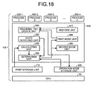
- FIG. 18 is a block diagram illustrating the structure of functions implemented by a CPU 20 provided in a processor 100 to execute an OS 500 and hardware components of the processor 100 .
- the OS 500 includes a resuming time update unit 580 , a state detecting unit 230 , a calculating unit 240 , a determining unit 250 , a second mode unit 260 , a first mode unit 565 , and a restore unit 570 .
- FIG. 18 represents that the processor 100 includes the hardware components, the OS 500 operated on the processor 100 , and one or more processes operated on the OS 500 .
- the first mode unit 565 has a function of notifying the resuming time update unit 580 of a shift in the state of the processor 100 to the sleep state when a request to temporarily stop the operation of the processor 100 is received from the determining unit 250 , in addition to the functions described in the first embodiment.
- the restore unit 570 has a function of notifying the resuming time update unit 580 of the resume of the operation of the processor 100 when the data saved in the storage area 900 by the first mode unit 565 is restored to the register 120 , in addition to the functions described in the first embodiment.
- the resuming time update unit 580 updates the value of the resuming time stored in the operation mode storage unit 220 according to characteristic information indicating the characteristics of the processor 100 during the period from the time when the processor 100 is shifted to the sleep state to the resume of the operation.
- characteristic information indicating the characteristics of the processor 100 during the period from the time when the processor 100 is shifted to the sleep state to the resume of the operation.
- the power consumption of the processor 100 is used as the characteristic information.
- the embodiment is not limited thereto, and any kind of characteristic information may be used.
- the temperature information of the processor 100 or the hit ratio of the cache may be used as the characteristic information. Any information necessary to change the resuming time stored in the operation mode storage unit 220 may be used as the characteristic information.
- FIG. 19 is a sequence diagram illustrating an example of a process from the request of the temporary stop of the processor 100 to a change in the resuming time stored in the operation mode storage unit 220 .
- the first mode unit 565 notifies the resuming time update unit 580 that the processor 100 is to be shifted to the sleep state (Step S 2001 ).
- the change unit 580 collects the characteristic information or various kinds of settings required to change the resuming time stored in the operation mode storage unit 220 (Step S 2002 ).
- the resuming time update unit 580 resets a measuring device that is capable of measuring the power consumption of the processor 100 for a specific period and directs the measuring device to measure the power consumption of the processor 100 from the time when the processor 100 is changed to the sleep state.
- the resuming time update unit 580 notifies the first mode unit 565 that the correction of various kinds of settings and the characteristic information has been completed (Step S 2003 ).
- the first mode unit 565 temporarily stops the operation of the processor 100 and shifts the state of the processor 100 to a power saving state (sleep state) (Step S 2004 ).
- the restore unit 570 restores the data, which is saved is the storage area 900 by the first mode unit 565 , to the register 120 (Step S 2010 ). Then, the restore unit 570 notifies the resuming time update unit 580 that the operation of the processor 100 has resumed (Step S 2011 ).
- the resuming time update unit 580 collects the characteristic information (Step S 2012 ). For example, the resuming time update unit 580 can acquire power consumption for the period from the time when the processor 100 is shifted to the sleep state to the current time from the measuring device.
- the resuming time update unit 580 updates the resuming time stored in the operation mode storage unit 220 on the basis of the collected characteristic information (Step S 2013 ). For example, if the resuming time is ty (>t 1 ) and power consumption W 2 when the processor 100 is maintained in the sleep state for the resuming time ty is significantly less than power consumption W 1 when the processor 100 is maintained in the idle state for a resuming time t 1 , it is preferable that the value of the resuming time indicating the shift conditions of the operation mode be less than t 1 .
- the resuming time update unit 580 notifies the restore unit 570 that the change in the resuming time has been completed (Step S 2014 ).
- the restore unit 570 proceeds to the process to be performed at the resume time (Step S 2015 ).
- the value of the resuming time stored in the operation mode storage unit 220 is set so as to vary depending on the power consumption (an example of the characteristic information) of the processor 100 for the period from the time when the processor 100 is shifted to the sleep state to the resume time of the operation. Therefore, it is possible to approximate the value of the resuming time stored in the operation mode storage unit 220 to the optimal value for the current target system.
- the value of the resuming time indicating the shift conditions of the operation mode which is stored in the operation mode storage unit 220 is fixed.
- the value of the resuming time stored in the operation mode storage unit 220 is variable, which will be described in detail below.
- the same components as those in the second embodiment and the fourth embodiment are denoted by the same reference numerals and a description thereof will not be repeated.
- FIG. 20 is a block diagram illustrating the structure of functions implemented by a CPU 20 provided in a processor 100 to execute an OS 600 and hardware components of the processor 100 .
- the OS 600 includes a resuming time update unit 680 , an interrupt waiting notifying unit 311 , a interrupt registration/removal unit 313 , a calculating unit 325 , a determining unit 250 , a second mode unit 260 , a state detecting unit 230 , a first mode unit 665 , a restore unit 670 , an interrupt processing unit 380 , and an interrupt waiting removal unit 390 .
- FIG. 20 represents that the processor 100 includes the hardware components, the OS 600 operated on the processor 100 , and one or more processes operated on the OS 600 .
- the first mode unit 665 has a function of notifying the resuming time update unit 680 of a shift in the state of the processor 100 to the sleep state when receiving a request to temporarily stop the operation of the processor 100 from the determining unit 250 , in addition to the functions described in the second embodiment.
- the restore unit 670 has a function of notifying the resuming time update unit 680 of the resume of the operation of the processor 100 when the data saved in the storage area 900 by the first mode unit 665 is restored to the register 120 , in addition to the functions described in the second embodiment.
- the resuming time update unit 680 updates the value of the resuming time stored in the operation mode storage unit 220 according to characteristic information indicating the characteristics of the processor 100 during the period from the time when the processor 100 is shifted to the sleep state and the time when the operation resumes.
- characteristic information indicating the characteristics of the processor 100 during the period from the time when the processor 100 is shifted to the sleep state and the time when the operation resumes.
- the power consumption of the processor 100 is used as the characteristic information.
- FIG. 21 is a sequence diagram illustrating an example of a process from the request of the temporary stop of the processor 100 to a change in the resuming time stored in the operation mode storage unit 220 .
- the first mode unit 665 when receiving a request to temporarily stop the operation of the processor 100 from the determining unit 250 (Step S 2100 ), the first mode unit 665 notifies the resuming time update unit 680 that the processor 100 is to be shifted to the sleep state (Step S 2101 ).
- the resuming time update unit 680 collects the characteristic information and various kinds of settings required to change the resuming time stored in the operation mode storage unit 220 (Step S 2102 ). This is the same as that of the collection process in the fourth embodiment. Then, the resuming time update unit 680 notifies the first mode unit 665 that the correction of various kinds of settings and the characteristic information has been completed (Step S 2103 ). When receiving the completion notice from the change unit 680 , the first mode unit 665 temporarily stops the operation of the processor 100 and shifts the state of the processor 100 to a power saving state (sleep state) (Step S 2104 ).
- the restore unit 670 restores the data, which is saved in the storage area 900 by the first mode unit 665 , to the register 120 (Step S 2110 ). Then, the restore unit 670 notifies the resuming time update unit 680 that the operation of the processor 100 has resumed (Step S 2111 ).
- the resuming time update unit 680 collects the characteristic information (Step S 2112 ). This is the same as that of the collection process in the fourth embodiment.
- the resuming time update unit 680 updates the resuming time stored in the operation mode storage unit 220 on the basis of the collected characteristic information (Step S 2113 ). This is the same as that of the change process in the fourth embodiment.
- the resuming time update unit 580 notifies the restore unit 670 that the change in the resuming time has been completed (Step S 2114 ).
- the restore unit 670 transmits an interrupt request to the interrupt processing unit 380 (Step S 2115 ).
- the value of the resuming time stored in the operation mode storage unit 220 is set so as to vary depending on the power consumption of the processor 100 for the period from the time when the processor 100 is shifted to the sleep state to the resume time of the operation. Therefore, it is possible to approximate the value of the resuming time stored in the operation mode storage unit 220 to the optimal value for the current target system.
- the resuming time is calculated from the timer information or by interrupt prediction, but embodiments are not limited thereto. It is only required that when the idle state of the processor 100 is detected, the resuming time indicating a time length until the next process starts is calculated and the operation mode is determined on the basis of the calculated resuming time.
- the shift conditions of the operation mode stored in the operation mode storage unit 220 are optional.
- the determining unit 250 may determine the operation mode of the processor 100 to be the second mode.
- the determining unit 250 may determine the operation mode of the processor 100 to be a third mode in which frequency control is performed by DVFS.
- the determining unit 250 may determine the operation mode of the processor 100 to be the first mode. The example shown in FIG. 22
- the determining unit 250 determines the operation of the processor 100 to be the first mode; and when the resuming time is equal to or less than the predetermined time length, t the determining unit 250 determines the operation of the processor 100 to be the second mode.
- the processor 100 includes the register 120 and the cache memory 140 which are volatile memories, but embodiments are not limited thereto.
- the processor 100 may not include the cache memory 140 .
- the register 120 or the cache memory 140 may be a non-volatile memory. According to this structure, it is possible to remove the process of saving the data stored in the register 120 or the cache memory 140 and the process of restoring the data.
- At least some of the functions of the OS may be implemented by hardware other than the processor 100 .
- the functions of the OS 200 according to the first embodiment may be implemented by a timer management unit 201 , which is a hardware component other than the processor 100 .
- FIG. 24 is a block diagram illustrating the structure of functions implemented by a CPU 30 of the timer management unit 201 to execute a program and hardware components of the timer management unit 201 .
- the hardware components of the timer management unit 201 includes the CPU 30 , a first storage unit 210 , and an operation mode storage unit 220 .
- the CPU 30 executes a program to implement the functions of a state detecting unit 230 , a calculating unit 240 , a determining unit 250 , a second mode unit 260 , a first mode unit 270 , and a restore unit 280 .
- the timer management unit 201 may be construed as a controller.
- FIG. 24 represents that the timer management unit 201 includes the hardware components, the OS operated on the timer management unit 201 , and one or more processes operated on the OS.
- Embodiments are not limited to the examples shown in FIGS. 23 and 24 .
- only some of the functions of the OS 200 may be implemented by hardware other than the processor 100 and the other functions may be implemented on the OS 200 .
Landscapes
- Engineering & Computer Science (AREA)
- Theoretical Computer Science (AREA)
- General Engineering & Computer Science (AREA)
- Physics & Mathematics (AREA)
- General Physics & Mathematics (AREA)
- Software Systems (AREA)
- Computer Hardware Design (AREA)
- Computing Systems (AREA)
- Power Sources (AREA)
Abstract
Description
Claims (8)
Applications Claiming Priority (2)
| Application Number | Priority Date | Filing Date | Title |
|---|---|---|---|
| JP2011065704A JP5284401B2 (en) | 2011-03-24 | 2011-03-24 | Operation switching device and program |
| JP2011-065704 | 2011-03-24 |
Publications (2)
| Publication Number | Publication Date |
|---|---|
| US20120246501A1 US20120246501A1 (en) | 2012-09-27 |
| US8868952B2 true US8868952B2 (en) | 2014-10-21 |
Family
ID=46878350
Family Applications (1)
| Application Number | Title | Priority Date | Filing Date |
|---|---|---|---|
| US13/345,824 Expired - Fee Related US8868952B2 (en) | 2011-03-24 | 2012-01-09 | Controller and program product |
Country Status (4)
| Country | Link |
|---|---|
| US (1) | US8868952B2 (en) |
| JP (1) | JP5284401B2 (en) |
| CN (1) | CN102722234B (en) |
| TW (1) | TWI468928B (en) |
Cited By (1)
| Publication number | Priority date | Publication date | Assignee | Title |
|---|---|---|---|---|
| US9710050B2 (en) | 2014-03-12 | 2017-07-18 | Kabushiki Kaisha Toshiba | Information processing device, semiconductor chip, information processing method, and computer program product |
Families Citing this family (25)
| Publication number | Priority date | Publication date | Assignee | Title |
|---|---|---|---|---|
| JP5674613B2 (en) | 2011-09-22 | 2015-02-25 | 株式会社東芝 | Control system, control method and program |
| JP5777467B2 (en) * | 2011-09-22 | 2015-09-09 | 株式会社東芝 | Control device and program |
| JP5674611B2 (en) | 2011-09-22 | 2015-02-25 | 株式会社東芝 | Control system, control method and program |
| JP2013149093A (en) | 2012-01-19 | 2013-08-01 | Toshiba Corp | Control device, control method, program, and electronic apparatus |
| US9326812B2 (en) | 2012-01-25 | 2016-05-03 | Covidien Lp | Portable surgical instrument |
| JP6007642B2 (en) * | 2012-01-26 | 2016-10-12 | 株式会社リコー | Information processing apparatus, power saving control method, power saving control program |
| JP6113538B2 (en) | 2012-03-23 | 2017-04-12 | 株式会社東芝 | Control device, control method, program, and semiconductor device |
| JP5677376B2 (en) | 2012-07-06 | 2015-02-25 | 株式会社東芝 | Memory control device, semiconductor device, and system board |
| JP5787852B2 (en) | 2012-09-07 | 2015-09-30 | 株式会社東芝 | Control device, information processing device, control method, and program |
| JP5696110B2 (en) | 2012-09-19 | 2015-04-08 | 株式会社東芝 | Power supply system, power supply control device, and program |
| JP5802637B2 (en) | 2012-09-21 | 2015-10-28 | 株式会社東芝 | Information processing apparatus, information processing method, and program |
| US8909836B2 (en) * | 2012-10-08 | 2014-12-09 | Andes Technology Corporation | Interrupt controller, apparatus including interrupt controller, and corresponding methods for processing interrupt request event(s) in system including processor(s) |
| JP6116941B2 (en) | 2013-02-28 | 2017-04-19 | 株式会社東芝 | Information processing device |
| JP6054203B2 (en) | 2013-02-28 | 2016-12-27 | 株式会社東芝 | Information processing apparatus, device control method, and program |
| JP6087662B2 (en) | 2013-02-28 | 2017-03-01 | 株式会社東芝 | Control device, control program, and information processing system |
| JP6071647B2 (en) | 2013-02-28 | 2017-02-01 | 株式会社東芝 | Information processing apparatus, operation state control method, and program |
| JP2015064676A (en) | 2013-09-24 | 2015-04-09 | 株式会社東芝 | Information processing device, semiconductor device, information processing method, and program |
| WO2015077981A1 (en) * | 2013-11-29 | 2015-06-04 | Intel Corporation | Power management in computing devices |
| US9507706B2 (en) * | 2013-12-03 | 2016-11-29 | Sandisk Technologies Llc | Memory system controller including a multi-resolution internal cache |
| US9354930B2 (en) * | 2014-04-11 | 2016-05-31 | Telefonaktiebolaget Lm Ericsson (Publ) | Scheduling of global voltage/frequency scaling switches among asynchronous dataflow dependent processors |
| JP2017111745A (en) * | 2015-12-18 | 2017-06-22 | ルネサスエレクトロニクス株式会社 | Semiconductor device, semiconductor system, and method for controlling the semiconductor device |
| US11625267B2 (en) * | 2017-08-02 | 2023-04-11 | Felica Networks, Inc. | Information processing apparatus and information processing method for changing contents of a process to be performed after an interrupt is detected |
| US10747298B2 (en) * | 2017-11-29 | 2020-08-18 | Advanced Micro Devices, Inc. | Dynamic interrupt rate control in computing system |
| CN114020140B (en) * | 2020-02-12 | 2023-11-28 | 地平线(上海)人工智能技术有限公司 | Method and device for controlling hardware module, electronic equipment and storage medium |
| EP3929740A1 (en) * | 2020-06-26 | 2021-12-29 | Siemens Aktiengesellschaft | Method for orchestrating a container-based application on a terminal |
Citations (7)
| Publication number | Priority date | Publication date | Assignee | Title |
|---|---|---|---|---|
| JPH03171217A (en) | 1989-11-30 | 1991-07-24 | Toshiba Corp | Resuming control system |
| JP2003029886A (en) | 2001-07-12 | 2003-01-31 | Denso Corp | Operating system, program and electronic controller for vehicle |
| US6889331B2 (en) | 2001-08-29 | 2005-05-03 | Analog Devices, Inc. | Dynamic voltage control method and apparatus |
| US20060031692A1 (en) | 2004-08-05 | 2006-02-09 | Kazuomi Kato | Power-saving processing unit, power-saving processing method and program record medium |
| JP2010113641A (en) | 2008-11-10 | 2010-05-20 | Fujitsu Ltd | Operation method of processor system and processor system |
| JP4644747B1 (en) | 2009-11-02 | 2011-03-02 | パナソニック株式会社 | Information processing apparatus, control method, and control program |
| US8181051B2 (en) * | 2006-02-09 | 2012-05-15 | Freescale Semiconductor, Inc. | Electronic apparatus and method of conserving energy |
Family Cites Families (3)
| Publication number | Priority date | Publication date | Assignee | Title |
|---|---|---|---|---|
| US7383457B1 (en) * | 2005-03-23 | 2008-06-03 | Apple Inc. | Adaptive power-reduction mode |
| CN101097482A (en) * | 2006-06-30 | 2008-01-02 | 佛山市顺德区顺达电脑厂有限公司 | Operation mode control system and method thereof |
| JP2008243220A (en) * | 2008-04-28 | 2008-10-09 | Renesas Technology Corp | Information processing communication device |
-
2011
- 2011-03-24 JP JP2011065704A patent/JP5284401B2/en not_active Expired - Fee Related
-
2012
- 2012-01-09 US US13/345,824 patent/US8868952B2/en not_active Expired - Fee Related
- 2012-02-22 TW TW101105893A patent/TWI468928B/en not_active IP Right Cessation
- 2012-03-23 CN CN201210080362.7A patent/CN102722234B/en not_active Expired - Fee Related
Patent Citations (11)
| Publication number | Priority date | Publication date | Assignee | Title |
|---|---|---|---|---|
| JPH03171217A (en) | 1989-11-30 | 1991-07-24 | Toshiba Corp | Resuming control system |
| JP2003029886A (en) | 2001-07-12 | 2003-01-31 | Denso Corp | Operating system, program and electronic controller for vehicle |
| US7386853B2 (en) | 2001-07-12 | 2008-06-10 | Denso Corporation | Multitasking operating system capable of reducing power consumption and vehicle electronic control unit using same |
| US6889331B2 (en) | 2001-08-29 | 2005-05-03 | Analog Devices, Inc. | Dynamic voltage control method and apparatus |
| JP2009064456A (en) | 2001-08-29 | 2009-03-26 | Mediatek Inc | Dynamic voltage control method and apparatus |
| US20060031692A1 (en) | 2004-08-05 | 2006-02-09 | Kazuomi Kato | Power-saving processing unit, power-saving processing method and program record medium |
| US7360106B2 (en) * | 2004-08-05 | 2008-04-15 | Matsushita Electric Industrial Co., Ltd. | Power-saving processing unit, power-saving processing method and program record medium |
| US8181051B2 (en) * | 2006-02-09 | 2012-05-15 | Freescale Semiconductor, Inc. | Electronic apparatus and method of conserving energy |
| JP2010113641A (en) | 2008-11-10 | 2010-05-20 | Fujitsu Ltd | Operation method of processor system and processor system |
| JP4644747B1 (en) | 2009-11-02 | 2011-03-02 | パナソニック株式会社 | Information processing apparatus, control method, and control program |
| US20120166833A1 (en) | 2009-11-02 | 2012-06-28 | Panasonic Corporation | Information processing device, control method and control program |
Non-Patent Citations (6)
| Title |
|---|
| Chinese Office Action for Chinese Application No. 201210080362.7 mailed Jun. 5, 2014. |
| English Translation of Japanese Office Action of Notice of Rejection for Application No. 2011-065704 Dated Feb. 12, 2013, 10 pgs. |
| Intel Document No. 316745-005, Intel Low Power Features "Clock Control and Low Power States", pp. 11-17. |
| Japanese Office Action for Japanese Application No. 2011-065704 mailed on Nov. 13, 2012. |
| Office Action for Taiwanese Patent Application No. 101105893 Dated Mar. 26, 2014, 12 pgs. |
| Sunata, Tetsuya, et al.; "Resource Management of Operating System for Fine Grain Power Gating Control", IPSJ SIG vol. 2010-OS-114 No. 8; 2010. |
Cited By (1)
| Publication number | Priority date | Publication date | Assignee | Title |
|---|---|---|---|---|
| US9710050B2 (en) | 2014-03-12 | 2017-07-18 | Kabushiki Kaisha Toshiba | Information processing device, semiconductor chip, information processing method, and computer program product |
Also Published As
| Publication number | Publication date |
|---|---|
| TWI468928B (en) | 2015-01-11 |
| CN102722234A (en) | 2012-10-10 |
| CN102722234B (en) | 2015-01-07 |
| JP2012203518A (en) | 2012-10-22 |
| TW201239610A (en) | 2012-10-01 |
| US20120246501A1 (en) | 2012-09-27 |
| JP5284401B2 (en) | 2013-09-11 |
Similar Documents
| Publication | Publication Date | Title |
|---|---|---|
| US8868952B2 (en) | Controller and program product | |
| US8725953B2 (en) | Local cache power control within a multiprocessor system | |
| US10281970B2 (en) | Control device, system, and computer program product | |
| US9904623B2 (en) | Early cache prefetching in preparation for exit from idle mode | |
| US9110671B2 (en) | Idle phase exit prediction | |
| KR101518440B1 (en) | Dynamic performance control of processing nodes | |
| US7861068B2 (en) | Method and apparatus for using dynamic workload characteristics to control CPU frequency and voltage scaling | |
| KR101673500B1 (en) | Method and apparatus for cache control | |
| EP3367212A1 (en) | Hardware automatic performance state transitions in system on processor sleep and wake events | |
| EP3332306B1 (en) | System and method for cache aware low power mode control in a portable computing device | |
| JP2016506576A (en) | Integrated circuit idle phase prediction. | |
| US9639045B2 (en) | Image forming apparatus that shifts to state where quick activation is possible, method of controlling the same, and storage medium | |
| WO2012158728A2 (en) | Adjusting the clock frequency of a processing unit in real-time based on a frequency sensitivity value | |
| US20200409610A1 (en) | Memory system | |
| US9959075B2 (en) | System and method for flush power aware low power mode control in a portable computing device | |
| US20180069767A1 (en) | Preserving quality of service constraints in heterogeneous processing systems | |
| US9625970B2 (en) | Information processing apparatus, operation state control method, and computer program product | |
| US20170322745A1 (en) | Information processing apparatus and method of controlling information processing apparatus | |
| US20170329626A1 (en) | Apparatus with at least one resource having thread mode and transaction mode, and method | |
| US20230376381A1 (en) | Checkpoint-progress status | |
| JPWO2011114495A1 (en) | Multi-core processor system, thread switching control method, and thread switching control program | |
| JPH11110063A (en) | Computer system | |
| GB2618355A (en) | Signalling power level threshold event to processing circuitry | |
| JP5582241B2 (en) | Multi-core processor system, multi-core processor system control method, and multi-core processor system control program | |
| US9424138B2 (en) | Checkpointing a computer hardware architecture state using a stack or queue |
Legal Events
| Date | Code | Title | Description |
|---|---|---|---|
| AS | Assignment |
Owner name: KABUSHIKI KAISHA TOSHIBA, JAPAN Free format text: ASSIGNMENT OF ASSIGNORS INTEREST;ASSIGNORS:HARUKI, HIROYOSHI;FUJISAKI, KOICHI;SHIRAI, SATOSHI;AND OTHERS;REEL/FRAME:027498/0817 Effective date: 20111219 |
|
| STCF | Information on status: patent grant |
Free format text: PATENTED CASE |
|
| FEPP | Fee payment procedure |
Free format text: PAYOR NUMBER ASSIGNED (ORIGINAL EVENT CODE: ASPN); ENTITY STATUS OF PATENT OWNER: LARGE ENTITY |
|
| AS | Assignment |
Owner name: TOSHIBA MEMORY CORPORATION, JAPAN Free format text: ASSIGNMENT OF ASSIGNORS INTEREST;ASSIGNOR:KABUSHIKI KAISHA TOSHIBA;REEL/FRAME:043709/0035 Effective date: 20170706 |
|
| MAFP | Maintenance fee payment |
Free format text: PAYMENT OF MAINTENANCE FEE, 4TH YEAR, LARGE ENTITY (ORIGINAL EVENT CODE: M1551) Year of fee payment: 4 |
|
| FEPP | Fee payment procedure |
Free format text: MAINTENANCE FEE REMINDER MAILED (ORIGINAL EVENT CODE: REM.); ENTITY STATUS OF PATENT OWNER: LARGE ENTITY |
|
| LAPS | Lapse for failure to pay maintenance fees |
Free format text: PATENT EXPIRED FOR FAILURE TO PAY MAINTENANCE FEES (ORIGINAL EVENT CODE: EXP.); ENTITY STATUS OF PATENT OWNER: LARGE ENTITY |
|
| STCH | Information on status: patent discontinuation |
Free format text: PATENT EXPIRED DUE TO NONPAYMENT OF MAINTENANCE FEES UNDER 37 CFR 1.362 |
|
| FP | Lapsed due to failure to pay maintenance fee |
Effective date: 20221021 |