US8564004B2 - Complex primary optics with intermediate elements - Google Patents
Complex primary optics with intermediate elements Download PDFInfo
- Publication number
- US8564004B2 US8564004B2 US13/306,589 US201113306589A US8564004B2 US 8564004 B2 US8564004 B2 US 8564004B2 US 201113306589 A US201113306589 A US 201113306589A US 8564004 B2 US8564004 B2 US 8564004B2
- Authority
- US
- United States
- Prior art keywords
- light emitter
- light
- intermediate element
- optic
- package
- Prior art date
- Legal status (The legal status is an assumption and is not a legal conclusion. Google has not performed a legal analysis and makes no representation as to the accuracy of the status listed.)
- Active
Links
- 239000008393 encapsulating agent Substances 0.000 claims abstract description 70
- 239000000463 material Substances 0.000 claims description 127
- 238000007493 shaping process Methods 0.000 claims description 17
- 238000006243 chemical reaction Methods 0.000 claims description 16
- 230000005499 meniscus Effects 0.000 claims description 16
- 229920003023 plastic Polymers 0.000 claims description 9
- 239000004033 plastic Substances 0.000 claims description 9
- 239000004372 Polyvinyl alcohol Substances 0.000 claims description 5
- 229920002451 polyvinyl alcohol Polymers 0.000 claims description 5
- 229920001169 thermoplastic Polymers 0.000 claims description 2
- 238000000034 method Methods 0.000 description 115
- 239000010410 layer Substances 0.000 description 71
- 230000003287 optical effect Effects 0.000 description 59
- 230000008569 process Effects 0.000 description 47
- 238000004519 manufacturing process Methods 0.000 description 32
- 239000000758 substrate Substances 0.000 description 32
- 238000000465 moulding Methods 0.000 description 27
- OAICVXFJPJFONN-UHFFFAOYSA-N Phosphorus Chemical compound [P] OAICVXFJPJFONN-UHFFFAOYSA-N 0.000 description 18
- 229920001296 polysiloxane Polymers 0.000 description 15
- 239000002245 particle Substances 0.000 description 11
- 238000013459 approach Methods 0.000 description 10
- 239000002904 solvent Substances 0.000 description 9
- 238000000605 extraction Methods 0.000 description 8
- 239000004593 Epoxy Substances 0.000 description 7
- 238000003491 array Methods 0.000 description 7
- 238000013461 design Methods 0.000 description 6
- 238000001746 injection moulding Methods 0.000 description 6
- 239000007788 liquid Substances 0.000 description 6
- 239000011521 glass Substances 0.000 description 5
- 229910052909 inorganic silicate Inorganic materials 0.000 description 5
- 229910052751 metal Inorganic materials 0.000 description 5
- 239000002184 metal Substances 0.000 description 5
- 238000000926 separation method Methods 0.000 description 5
- 229910019655 synthetic inorganic crystalline material Inorganic materials 0.000 description 5
- 230000008901 benefit Effects 0.000 description 4
- 238000000576 coating method Methods 0.000 description 4
- 150000001875 compounds Chemical class 0.000 description 4
- 238000003754 machining Methods 0.000 description 4
- 235000019422 polyvinyl alcohol Nutrition 0.000 description 4
- 238000004088 simulation Methods 0.000 description 4
- XLYOFNOQVPJJNP-UHFFFAOYSA-N water Substances O XLYOFNOQVPJJNP-UHFFFAOYSA-N 0.000 description 4
- 230000009471 action Effects 0.000 description 3
- 239000011248 coating agent Substances 0.000 description 3
- 229920002120 photoresistant polymer Polymers 0.000 description 3
- 238000007639 printing Methods 0.000 description 3
- 238000001228 spectrum Methods 0.000 description 3
- 239000012780 transparent material Substances 0.000 description 3
- 238000001429 visible spectrum Methods 0.000 description 3
- 229910052727 yttrium Inorganic materials 0.000 description 3
- 229910019901 yttrium aluminum garnet Inorganic materials 0.000 description 3
- 238000010146 3D printing Methods 0.000 description 2
- XUIMIQQOPSSXEZ-UHFFFAOYSA-N Silicon Chemical compound [Si] XUIMIQQOPSSXEZ-UHFFFAOYSA-N 0.000 description 2
- FAPWRFPIFSIZLT-UHFFFAOYSA-M Sodium chloride Chemical compound [Na+].[Cl-] FAPWRFPIFSIZLT-UHFFFAOYSA-M 0.000 description 2
- 238000010521 absorption reaction Methods 0.000 description 2
- 230000015572 biosynthetic process Effects 0.000 description 2
- 230000015556 catabolic process Effects 0.000 description 2
- 239000000919 ceramic Substances 0.000 description 2
- 238000003486 chemical etching Methods 0.000 description 2
- 238000000748 compression moulding Methods 0.000 description 2
- 238000006731 degradation reaction Methods 0.000 description 2
- 230000001419 dependent effect Effects 0.000 description 2
- 238000000151 deposition Methods 0.000 description 2
- 230000008021 deposition Effects 0.000 description 2
- 238000000295 emission spectrum Methods 0.000 description 2
- 229910052733 gallium Inorganic materials 0.000 description 2
- 230000005484 gravity Effects 0.000 description 2
- 239000000203 mixture Substances 0.000 description 2
- 239000006082 mold release agent Substances 0.000 description 2
- 230000005404 monopole Effects 0.000 description 2
- 239000013307 optical fiber Substances 0.000 description 2
- 238000000206 photolithography Methods 0.000 description 2
- 229920000515 polycarbonate Polymers 0.000 description 2
- 239000004417 polycarbonate Substances 0.000 description 2
- 230000009467 reduction Effects 0.000 description 2
- 229920006395 saturated elastomer Polymers 0.000 description 2
- 239000004065 semiconductor Substances 0.000 description 2
- 229910052710 silicon Inorganic materials 0.000 description 2
- 239000010703 silicon Substances 0.000 description 2
- 239000007787 solid Substances 0.000 description 2
- 238000005507 spraying Methods 0.000 description 2
- 238000000859 sublimation Methods 0.000 description 2
- 230000008022 sublimation Effects 0.000 description 2
- 239000000126 substance Substances 0.000 description 2
- 230000003319 supportive effect Effects 0.000 description 2
- 238000001721 transfer moulding Methods 0.000 description 2
- 230000007704 transition Effects 0.000 description 2
- 238000009834 vaporization Methods 0.000 description 2
- 230000008016 vaporization Effects 0.000 description 2
- 229910052693 Europium Inorganic materials 0.000 description 1
- 229910052688 Gadolinium Inorganic materials 0.000 description 1
- 229910052765 Lutetium Inorganic materials 0.000 description 1
- VYPSYNLAJGMNEJ-UHFFFAOYSA-N Silicium dioxide Chemical compound O=[Si]=O VYPSYNLAJGMNEJ-UHFFFAOYSA-N 0.000 description 1
- 229910004412 SrSi2 Inorganic materials 0.000 description 1
- 229910002370 SrTiO3 Inorganic materials 0.000 description 1
- 229920002472 Starch Polymers 0.000 description 1
- 229910001315 Tool steel Inorganic materials 0.000 description 1
- NIXOWILDQLNWCW-UHFFFAOYSA-N acrylic acid group Chemical group C(C=C)(=O)O NIXOWILDQLNWCW-UHFFFAOYSA-N 0.000 description 1
- JNDMLEXHDPKVFC-UHFFFAOYSA-N aluminum;oxygen(2-);yttrium(3+) Chemical compound [O-2].[O-2].[O-2].[Al+3].[Y+3] JNDMLEXHDPKVFC-UHFFFAOYSA-N 0.000 description 1
- 230000009286 beneficial effect Effects 0.000 description 1
- 238000007664 blowing Methods 0.000 description 1
- 229910019990 cerium-doped yttrium aluminum garnet Inorganic materials 0.000 description 1
- 230000008859 change Effects 0.000 description 1
- 239000003086 colorant Substances 0.000 description 1
- 238000011109 contamination Methods 0.000 description 1
- 229920001577 copolymer Polymers 0.000 description 1
- 238000005260 corrosion Methods 0.000 description 1
- 230000007797 corrosion Effects 0.000 description 1
- 239000013078 crystal Substances 0.000 description 1
- 238000005137 deposition process Methods 0.000 description 1
- 238000011161 development Methods 0.000 description 1
- 238000009826 distribution Methods 0.000 description 1
- 239000000428 dust Substances 0.000 description 1
- 230000000694 effects Effects 0.000 description 1
- 230000005670 electromagnetic radiation Effects 0.000 description 1
- 238000001652 electrophoretic deposition Methods 0.000 description 1
- 230000007613 environmental effect Effects 0.000 description 1
- 125000003700 epoxy group Chemical group 0.000 description 1
- -1 etc.) Substances 0.000 description 1
- 238000005530 etching Methods 0.000 description 1
- 230000005284 excitation Effects 0.000 description 1
- 238000001125 extrusion Methods 0.000 description 1
- 239000000945 filler Substances 0.000 description 1
- 238000011049 filling Methods 0.000 description 1
- 239000011888 foil Substances 0.000 description 1
- 229910021485 fumed silica Inorganic materials 0.000 description 1
- 238000010348 incorporation Methods 0.000 description 1
- 238000002329 infrared spectrum Methods 0.000 description 1
- 238000002347 injection Methods 0.000 description 1
- 239000007924 injection Substances 0.000 description 1
- 229910010272 inorganic material Inorganic materials 0.000 description 1
- 239000011147 inorganic material Substances 0.000 description 1
- 230000001788 irregular Effects 0.000 description 1
- 229910052746 lanthanum Inorganic materials 0.000 description 1
- 230000033001 locomotion Effects 0.000 description 1
- 229910003443 lutetium oxide Inorganic materials 0.000 description 1
- 230000014759 maintenance of location Effects 0.000 description 1
- 230000007246 mechanism Effects 0.000 description 1
- 239000012528 membrane Substances 0.000 description 1
- 239000007769 metal material Substances 0.000 description 1
- 150000002739 metals Chemical class 0.000 description 1
- 230000004048 modification Effects 0.000 description 1
- 238000012986 modification Methods 0.000 description 1
- 238000009740 moulding (composite fabrication) Methods 0.000 description 1
- 239000011368 organic material Substances 0.000 description 1
- 238000001020 plasma etching Methods 0.000 description 1
- 229920003229 poly(methyl methacrylate) Polymers 0.000 description 1
- 229920000647 polyepoxide Polymers 0.000 description 1
- 229920000642 polymer Polymers 0.000 description 1
- 229920002959 polymer blend Polymers 0.000 description 1
- 239000004926 polymethyl methacrylate Substances 0.000 description 1
- 238000012545 processing Methods 0.000 description 1
- 238000010008 shearing Methods 0.000 description 1
- 239000002356 single layer Substances 0.000 description 1
- 239000011780 sodium chloride Substances 0.000 description 1
- 229910000679 solder Inorganic materials 0.000 description 1
- 239000002195 soluble material Substances 0.000 description 1
- 239000000243 solution Substances 0.000 description 1
- 230000003595 spectral effect Effects 0.000 description 1
- 238000004528 spin coating Methods 0.000 description 1
- 239000008107 starch Substances 0.000 description 1
- 235000019698 starch Nutrition 0.000 description 1
- 230000003746 surface roughness Effects 0.000 description 1
- 238000002211 ultraviolet spectrum Methods 0.000 description 1
- 229910052725 zinc Inorganic materials 0.000 description 1
Images
Classifications
-
- H—ELECTRICITY
- H01—ELECTRIC ELEMENTS
- H01L—SEMICONDUCTOR DEVICES NOT COVERED BY CLASS H10
- H01L33/00—Semiconductor devices having potential barriers specially adapted for light emission; Processes or apparatus specially adapted for the manufacture or treatment thereof or of parts thereof; Details thereof
- H01L33/48—Semiconductor devices having potential barriers specially adapted for light emission; Processes or apparatus specially adapted for the manufacture or treatment thereof or of parts thereof; Details thereof characterised by the semiconductor body packages
- H01L33/52—Encapsulations
- H01L33/54—Encapsulations having a particular shape
-
- B—PERFORMING OPERATIONS; TRANSPORTING
- B29—WORKING OF PLASTICS; WORKING OF SUBSTANCES IN A PLASTIC STATE IN GENERAL
- B29C—SHAPING OR JOINING OF PLASTICS; SHAPING OF MATERIAL IN A PLASTIC STATE, NOT OTHERWISE PROVIDED FOR; AFTER-TREATMENT OF THE SHAPED PRODUCTS, e.g. REPAIRING
- B29C33/00—Moulds or cores; Details thereof or accessories therefor
- B29C33/44—Moulds or cores; Details thereof or accessories therefor with means for, or specially constructed to facilitate, the removal of articles, e.g. of undercut articles
- B29C33/52—Moulds or cores; Details thereof or accessories therefor with means for, or specially constructed to facilitate, the removal of articles, e.g. of undercut articles soluble or fusible
-
- B—PERFORMING OPERATIONS; TRANSPORTING
- B29—WORKING OF PLASTICS; WORKING OF SUBSTANCES IN A PLASTIC STATE IN GENERAL
- B29C—SHAPING OR JOINING OF PLASTICS; SHAPING OF MATERIAL IN A PLASTIC STATE, NOT OTHERWISE PROVIDED FOR; AFTER-TREATMENT OF THE SHAPED PRODUCTS, e.g. REPAIRING
- B29C43/00—Compression moulding, i.e. applying external pressure to flow the moulding material; Apparatus therefor
- B29C43/02—Compression moulding, i.e. applying external pressure to flow the moulding material; Apparatus therefor of articles of definite length, i.e. discrete articles
- B29C43/18—Compression moulding, i.e. applying external pressure to flow the moulding material; Apparatus therefor of articles of definite length, i.e. discrete articles incorporating preformed parts or layers, e.g. compression moulding around inserts or for coating articles
-
- B—PERFORMING OPERATIONS; TRANSPORTING
- B29—WORKING OF PLASTICS; WORKING OF SUBSTANCES IN A PLASTIC STATE IN GENERAL
- B29C—SHAPING OR JOINING OF PLASTICS; SHAPING OF MATERIAL IN A PLASTIC STATE, NOT OTHERWISE PROVIDED FOR; AFTER-TREATMENT OF THE SHAPED PRODUCTS, e.g. REPAIRING
- B29C45/00—Injection moulding, i.e. forcing the required volume of moulding material through a nozzle into a closed mould; Apparatus therefor
- B29C45/17—Component parts, details or accessories; Auxiliary operations
- B29C45/40—Removing or ejecting moulded articles
- B29C45/44—Removing or ejecting moulded articles for undercut articles
- B29C45/4457—Removing or ejecting moulded articles for undercut articles using fusible, soluble or destructible cores
-
- G—PHYSICS
- G02—OPTICS
- G02B—OPTICAL ELEMENTS, SYSTEMS OR APPARATUS
- G02B19/00—Condensers, e.g. light collectors or similar non-imaging optics
- G02B19/0004—Condensers, e.g. light collectors or similar non-imaging optics characterised by the optical means employed
- G02B19/0028—Condensers, e.g. light collectors or similar non-imaging optics characterised by the optical means employed refractive and reflective surfaces, e.g. non-imaging catadioptric systems
-
- G—PHYSICS
- G02—OPTICS
- G02B—OPTICAL ELEMENTS, SYSTEMS OR APPARATUS
- G02B19/00—Condensers, e.g. light collectors or similar non-imaging optics
- G02B19/0033—Condensers, e.g. light collectors or similar non-imaging optics characterised by the use
- G02B19/0047—Condensers, e.g. light collectors or similar non-imaging optics characterised by the use for use with a light source
- G02B19/0061—Condensers, e.g. light collectors or similar non-imaging optics characterised by the use for use with a light source the light source comprising a LED
- G02B19/0066—Condensers, e.g. light collectors or similar non-imaging optics characterised by the use for use with a light source the light source comprising a LED in the form of an LED array
-
- B—PERFORMING OPERATIONS; TRANSPORTING
- B29—WORKING OF PLASTICS; WORKING OF SUBSTANCES IN A PLASTIC STATE IN GENERAL
- B29C—SHAPING OR JOINING OF PLASTICS; SHAPING OF MATERIAL IN A PLASTIC STATE, NOT OTHERWISE PROVIDED FOR; AFTER-TREATMENT OF THE SHAPED PRODUCTS, e.g. REPAIRING
- B29C33/00—Moulds or cores; Details thereof or accessories therefor
- B29C33/56—Coatings, e.g. enameled or galvanised; Releasing, lubricating or separating agents
- B29C33/68—Release sheets
-
- B—PERFORMING OPERATIONS; TRANSPORTING
- B29—WORKING OF PLASTICS; WORKING OF SUBSTANCES IN A PLASTIC STATE IN GENERAL
- B29C—SHAPING OR JOINING OF PLASTICS; SHAPING OF MATERIAL IN A PLASTIC STATE, NOT OTHERWISE PROVIDED FOR; AFTER-TREATMENT OF THE SHAPED PRODUCTS, e.g. REPAIRING
- B29C45/00—Injection moulding, i.e. forcing the required volume of moulding material through a nozzle into a closed mould; Apparatus therefor
- B29C45/14—Injection moulding, i.e. forcing the required volume of moulding material through a nozzle into a closed mould; Apparatus therefor incorporating preformed parts or layers, e.g. injection moulding around inserts or for coating articles
- B29C45/14639—Injection moulding, i.e. forcing the required volume of moulding material through a nozzle into a closed mould; Apparatus therefor incorporating preformed parts or layers, e.g. injection moulding around inserts or for coating articles for obtaining an insulating effect, e.g. for electrical components
- B29C45/14655—Injection moulding, i.e. forcing the required volume of moulding material through a nozzle into a closed mould; Apparatus therefor incorporating preformed parts or layers, e.g. injection moulding around inserts or for coating articles for obtaining an insulating effect, e.g. for electrical components connected to or mounted on a carrier, e.g. lead frame
-
- B—PERFORMING OPERATIONS; TRANSPORTING
- B33—ADDITIVE MANUFACTURING TECHNOLOGY
- B33Y—ADDITIVE MANUFACTURING, i.e. MANUFACTURING OF THREE-DIMENSIONAL [3-D] OBJECTS BY ADDITIVE DEPOSITION, ADDITIVE AGGLOMERATION OR ADDITIVE LAYERING, e.g. BY 3-D PRINTING, STEREOLITHOGRAPHY OR SELECTIVE LASER SINTERING
- B33Y80/00—Products made by additive manufacturing
-
- H—ELECTRICITY
- H01—ELECTRIC ELEMENTS
- H01L—SEMICONDUCTOR DEVICES NOT COVERED BY CLASS H10
- H01L2224/00—Indexing scheme for arrangements for connecting or disconnecting semiconductor or solid-state bodies and methods related thereto as covered by H01L24/00
- H01L2224/01—Means for bonding being attached to, or being formed on, the surface to be connected, e.g. chip-to-package, die-attach, "first-level" interconnects; Manufacturing methods related thereto
- H01L2224/42—Wire connectors; Manufacturing methods related thereto
- H01L2224/47—Structure, shape, material or disposition of the wire connectors after the connecting process
- H01L2224/48—Structure, shape, material or disposition of the wire connectors after the connecting process of an individual wire connector
- H01L2224/4805—Shape
- H01L2224/4809—Loop shape
- H01L2224/48091—Arched
-
- H—ELECTRICITY
- H01—ELECTRIC ELEMENTS
- H01L—SEMICONDUCTOR DEVICES NOT COVERED BY CLASS H10
- H01L2933/00—Details relating to devices covered by the group H01L33/00 but not provided for in its subgroups
- H01L2933/0008—Processes
- H01L2933/0033—Processes relating to semiconductor body packages
- H01L2933/005—Processes relating to semiconductor body packages relating to encapsulations
-
- H—ELECTRICITY
- H01—ELECTRIC ELEMENTS
- H01L—SEMICONDUCTOR DEVICES NOT COVERED BY CLASS H10
- H01L33/00—Semiconductor devices having potential barriers specially adapted for light emission; Processes or apparatus specially adapted for the manufacture or treatment thereof or of parts thereof; Details thereof
- H01L33/48—Semiconductor devices having potential barriers specially adapted for light emission; Processes or apparatus specially adapted for the manufacture or treatment thereof or of parts thereof; Details thereof characterised by the semiconductor body packages
- H01L33/58—Optical field-shaping elements
Definitions
- the present invention relates to fabricating light emitter packages and optical elements and, more specifically, to primary optics and packages for LED devices and methods of manufacturing such optics and packages.
- LEDs Light emitting diodes
- LEDs are solid state devices that convert electric energy to light, and generally comprise one or more active layers of semiconductor material sandwiched between oppositely doped layers. When a bias is applied across the doped layers, holes and electrons are injected into the active layer where they recombine to generate light. Light is emitted from the active layer and from all surfaces of the LED.
- the useful light is generally emitted in a hemispherical emission pattern in the direction of the LED's top surface, typically resulting in a predominantly Lambertian light emission profile. This confined emission is not generally suitable for many applications such as those requiring specific beam shaping; for example, collimated beam profiles, dispersed beam profiles, or specialized beam profiles.
- LEDs are typically arranged in a package which encases and protects the LED and provides electrical and thermal contact as well as enhances the emission of light from the LED.
- LED packages typically incorporate some type of encapsulant such as a transparent epoxy or silicone material surrounding the LED chip to enhance light extraction from the chip and protect the chip and related contacts structure (e.g. wire bonds) from exposure to physical damage or environmental conditions which could lead to corrosion or degradation.
- encapsulant such as a transparent epoxy or silicone material surrounding the LED chip to enhance light extraction from the chip and protect the chip and related contacts structure (e.g. wire bonds) from exposure to physical damage or environmental conditions which could lead to corrosion or degradation.
- LED packages may also incorporate a ‘primary’ optical element to enhance light extraction from the package and in some instances to provide output light beam shaping by controlling the angle-dependent emission properties of the lamp.
- the primary optical element typically has a predominantly hemispherical profile and may be formed by shaping the encapsulant (e.g., by a molding process), or may comprise a separately fabricated optical element (e.g., a molded glass or silicone lens) that may be mounted to the package—typically in contact with the encapsulant material.
- LEDs intended for lower-power applications such as signal or indicator lights are often arranged in packages that can include a molded or cast plastic body that encapsulates an LED chip, a lens, and conductive traces or leads. Heat is typically generated by LEDs when power is applied and the LEDs are emitting light.
- the traces or leads serve as a conduit to supply the LED chip with electrical power and can also serve to draw heat away from the LED chip.
- a portion of the lead frame extends out of the package for connection to circuits external to the lead frame package.
- a common configuration is the “surface mount” package which incorporates one or more LED chips mounted onto a planar substrate.
- Such packages typically include an appropriate encapsulant material (e.g., silicone) as well as a primary optic element.
- the primary optic element may be produced by forming the encapsulant material into a specified shape as it is added to the package—for example by molding the silicone encapsulant into a hemispherical shape using a process such as injection molding. Alternately, a separate glass or molded silicone lens may be applied to the package.
- the possible lens and encapsulant materials typically include silicones and glasses.
- the lens typically comprises a solid hemisphere with a substantially flat or planar surface which is mounted above the LED chip to allow clearance for the LED chip wire bonds.
- a supportive element's retention features to retain the lens against lateral forces it may be necessary for a retaining feature to rise above the bottom surface and surround the lower portion of the lens.
- the hemispherical lens sits within a recessed lip of the reflector plate.
- this retaining feature is typically not transparent to light but rather is reflective. This arrangement can result in some of the light emitted by the LED chip being lost due to loss mechanisms such as total internal reflection.
- additional reflective surfaces are required to direct sideways emitted LED light to the lens and out the package. This reflection process is not 100% efficient, resulting in additional loss of light. Also, reflections from these surfaces effectively create a larger, more complex light source (compared, for example, to the chip alone) which can require more complex secondary optics that can result in additional light loss.
- the primary optical elements and associated encapsulant materials of surface mount LED packages typically surround or encapsulate one or more LED chips and any associated electrical contacts.
- the preferred geometry for the primary optical element 10 has been a predominantly hemispherical shape, as shown in FIGS. 1 a - 1 e .
- This shape has two primary benefits: (1) if large enough relative to the LED source, most of the light emitted by the LED is incident on the optic surface with a path that is nearly parallel to the surface normal (since the optic is typically surrounded by air and has an index of refraction higher than air, this minimizes the possibility of total internal reflection and hence efficiency loss), and (2) hemispherical shapes are readily fabricated onto planar surfaces by conventional molding processes. If the diameter of the hemispherical optic is not large compared to the largest dimension of the associated LED source, the package may suffer from output losses caused by total internal reflection (“TIR”) within the optic, resulting in a low package extraction efficiency.
- TIR total internal reflection
- the hemispherical optic 10 geometry is desirable with respect to efficiency and ease of fabrication, this geometry typically does little to modify the initial optical output beam profile from the LED source.
- the light output from the package may be predominantly Lambertian in nature, as shown in FIGS. 2 A and 2 B—similar to that emitted by a typical LED.
- a substantially non-Lambertian light beam profile e.g., collimated, dispersed, or otherwise shaped
- a primary optic centered over a predominantly Lambertian emitting source such as a typical LED or array of LEDs
- many such geometries are not readily fabricated by molding processes. Specifically, since the mold cavity must be removed from the substrate surface following curing of the molded optic, it is not generally possible to mold parts which have ‘overhangs’, are tapered, or are narrower at the base (near the substrate) than at the top.
- a mold 108 is applied to a planar substrate 100 with associated LED chips 102 .
- the cavities in the mold are filled with a suitable encapsulating/optical material such as silicone or epoxy.
- the encapsulant is then at least partially cured, and the mold removed, leaving behind encapsulant on the surface in the form of a primary optical element.
- a suitable encapsulating/optical material such as silicone or epoxy.
- beam shaping for LED packages is typically achieved through the use of “secondary” optics.
- secondary optics generally increase overall cost and reduce efficiency.
- shape of the secondary optic can be limited by the size and geometry of the primary LED optic or lens—this can further reduce efficiency and limit the potential for beam shaping in some applications, particularly those involving collimation of the LED light, where it is helpful to bring the optical element as close to the light source (LED chip or chips) as possible.
- the use of secondary optics can result in lighting solutions which are bulky, require additional design work and alignment, optical loss, and additional costs.
- a secondary optical element is required (e.g., if the required light beam profile necessitates an optical element which is too large to conveniently or economically fabricate as a primary optical element on a LED package).
- the ability to fabricate a more complex primary optic may still find application in that the geometry of the primary optic may be tailored to produce an optical beam profile which reduces the constraints on the design of the secondary optical element, thereby enabling, for example, a lower cost or less bulky, more simplified secondary optic and reducing overall system costs.
- the present invention provides various embodiments of optics and methods of fabricating the same such that these optics are capable of beam shaping and can be manufactured in batches or arrays. Furthermore, these optics may include overhangs or tapered shapes without the need for complex molds with moving parts.
- One embodiment according to the present invention of a method for fabricating a light emitter package comprises providing a surface with a light emitter. Next, at least one intermediate element at least partially surrounding the light emitter and creating a cavity is provided. Following this step an encapsulant material is provided over the light emitter in the cavity, covering at least part of the light emitter such that the shape of the encapsulant is at least partially defined by the intermediate element. Lastly, the encapsulant is at least partially cured to form a primary optic.
- a light emitter package comprising a light emitter disposed on a surface.
- the package further comprises at least one intermediate element on the surface which at least partially surrounds the light emitter.
- the package includes an encapsulant over the light emitter forming a primary optic, where the intermediate element at least partially defines the shape of the primary optic.
- inventions according to the present invention also include arrays of packages and fabrication of arrays of these packages.
- FIG. 1 a is a side view of an embodiment of a traditional LED package with a hemispherical primary optical element or lens.
- FIG. 1 b is a top view of an embodiment of a traditional LED package with a hemispherical primary optical element or lens.
- FIG. 1 c is a side view of the first step in an embodiment of fabricating a traditional LED package with a hemispherical primary optical element or lens.
- FIG. 1 d is a side view of the second step in an embodiment of fabricating a traditional LED package with a hemispherical primary optical element or lens.
- FIG. 1 e is a side view of the third step in an embodiment of fabricating a traditional LED package with a hemispherical primary optical element or lens.
- FIG. 2 a is a side view of an embodiment of a traditional LED package with a hemispherical primary optical element or lens with simulated light rays.
- FIG. 2 b is a chart demonstrating the intensity slice data of light output of a traditional LED package with a hemispherical primary optical element or lens with simulated light rays.
- FIG. 3 a is a rotated side view of an embodiment of a light emitter package with primary optic according to the present invention.
- FIG. 3 b is a side view of an embodiment of a light emitter package with primary optic according to the present invention.
- FIG. 3 c is a top view of an embodiment of a light emitter package with primary optic according to the present invention.
- FIG. 3 d is a perspective view of an embodiment of a light emitter package with primary optic according to the present invention.
- FIG. 3 e is a side view of an embodiment of a light emitter package with primary optic with simulated light ray output according to the present invention.
- FIG. 3 f is a side view of another embodiment of a light emitter package with primary optic with simulated light ray output according to the present invention.
- FIG. 3 g is a chart demonstrating the intensity slice data of light output of the package of FIG. 3 e with simulated light rays according to the present invention.
- FIG. 4 is a side view of one embodiment of a surface with light emitters according to the present invention.
- FIG. 5 is a side view of one embodiment of intermediate elements according to the present invention.
- FIG. 6 is a top view of one embodiment of an intermediate element panel according to the present invention.
- FIG. 7 is a side view of one embodiment of a surface with intermediate elements and light emitters according to the present invention.
- FIG. 8 is a side view of one embodiment of encapsulant material being dispensed over the structure of FIG. 7 according to the present invention.
- FIG. 9 is a side view of the structure of FIG. 8 placed in solvent in one embodiment of a removal process according to the present invention.
- FIG. 10 is a side view of one embodiment of a package separation process according to the present invention.
- FIG. 11 is a side view of one embodiment of a surface with elements and intermediate material according to the present invention.
- FIG. 12 is a side view of one embodiment of a mold over the structure of FIG. 11 according to the present invention.
- FIG. 13 is a side view of one embodiment of completed optics formed from the structure of FIG. 12 according to the present invention.
- FIG. 14 is a side view of one embodiment of a surface with elements and intermediate material according to the present invention.
- FIG. 15 is a side view of one embodiment of a mold over the structure of FIG. 14 according to the present invention.
- FIG. 16 a is a side view of one embodiment of completed optics formed from the structure of FIG. 15 according to the present invention.
- FIG. 16 b is a side view of one embodiment of completed optics according to the present invention.
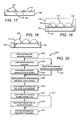
- FIG. 17 is a side view of one embodiment of a surface with elements and intermediate material according to the present invention.
- FIG. 18 is a side view of one embodiment of a mold over the structure of FIG. 17 according to the present invention.
- FIG. 19 is a side view of one embodiment of completed optics formed from the structure of FIG. 18 according to the present invention.
- FIG. 20 is a flow chart depicting one embodiment of an optic fabrication process according to the present invention.
- FIG. 21 is a flow chart depicting another embodiment of an optic fabrication process according to the present invention.
- FIG. 22 is a side view of one embodiment of intermediate elements according to the present invention.
- FIG. 23 is a top view of one embodiment of an intermediate element panel according to the present invention.
- FIG. 24 is a side view of one embodiment of a molding process according to the present invention.
- FIG. 25 is a side view of one embodiment of encapsulant material being dispensed over the structure of FIG. 24 according to the present invention.
- FIG. 26 is a side view of one embodiment of completion of the structure of FIG. 25 according the present invention.
- FIG. 27 is a side view of the structure of FIG. 26 placed in solvent in one embodiment of a removal process according to the present invention.
- FIG. 28 is a side view of one embodiment of a package separation process according to the present invention.
- FIG. 29 is a flow chart depicting another embodiment of an optic fabrication process according to the present invention.
- FIG. 30 is a side view of one embodiment of a surface with elements and intermediate material according to the present invention.
- FIG. 31 is a side view of one embodiment of an encapsulant dispense process over the structure of FIG. 30 according to the present invention.
- FIG. 32 is a side view of one embodiment of completed optics formed from the structure of FIG. 31 according to the present invention.
- FIG. 33 is a side view of one embodiment of completed optics formed with a support ring according to the present invention
- FIG. 34 is a cross-sectional view of one embodiment of an optic fabricated from a process according to the present invention.
- FIG. 35 is a cross-sectional view of another embodiment of an optic fabricated from a process according to the present invention.
- FIG. 36 is a cross-sectional view of another embodiment of an optic fabricated from a process according to the present invention.
- FIG. 37 is a side view of another embodiment of optics fabricated from a process according to the present invention.
- Embodiments of the present invention provide improved light emitting device optics and packages and methods for fabricating the same, wherein the improvements are provided by fabricating more complex primary optics capable of shaping light beams over light emitters.
- the primary optics disclosed herein, and methods of fabricating the same allow for more controlled or shaped light outputs from light emitters without the use of secondary optics.
- secondary optics may still be used in conjunction with these primary optics.
- the methods disclosed herein allow for the fabrication of arrays of optics according to the present invention in smaller areas because no moving parts or side action molds are required.
- Embodiments of the present invention may be used in combination with previously disclosed light extraction and optic approaches, allowing even greater flexibility in controlling the light emission pattern from LED devices.
- the invention may be applied to other light sources such as lasers, optical fibers, etc. or even to non-light emitting applications (e.g., camera phone lenses, etc.) where it is desirable to fabricate a complex optical element onto a surface.
- the present invention is described below with reference to forming complex primary optics capable of shaping light beams over light emitters. It is understood, that the present invention can be used in forming lenses in many other applications. For example, the present invention can used to form optics that collect rather than shape light from light emitters. This can be used in many different applications such as a concentrating lens on a miniature solar cell, or for a cell-phone camera lens. Accordingly, the present invention should not be limited to primary optics over light emitters.
- first, second, etc. may be used herein to describe various elements, components, regions, layers and/or sections, these elements, components, regions, layers and/or sections should not be limited by these terms. These terms are only used to distinguish one element, component, region, layer or section from another. Thus, a first element, component, region, layer or section discussed below could be termed a second element, component, region, layer or section without departing from the teachings of the present invention.
- ⁇ and “layers” are used interchangeably throughout the application.
- a person of ordinary skill in the art will understand that a single “layer” of material may actually comprise several individual layers of material. Likewise, several “layers” of material may be considered functionally as a single layer. In other words the term “layer” does not denote a homogenous layer of material.
- a single “layer” may contain various material concentrations and compositions that are localized in sub-layers. These sub-layers may be formed in a single formation step or in multiple steps. Unless specifically stated otherwise, it is not intended to limit the scope of the invention as embodied in the claims by describing an element as comprising a “layer” or “layers” of material.
- Embodiments of the invention are described herein with reference to cross-sectional view illustrations that are schematic illustrations of idealized embodiments of the invention. As such, variations from the shapes of the illustrations as a result, for example, of manufacturing techniques and/or tolerances are expected. Embodiments of the invention should not be construed as limited to the particular shapes of the regions or particles illustrated herein but are to include deviations in shapes that result, for example, from manufacturing. A region illustrated or described as rectangular, for example, will typically have rounded or curved features due to normal manufacturing techniques. Thus, the regions illustrated in the figures are schematic in nature; their shapes are not intended to illustrate the precise shape of a region or particle and are not intended to limit the scope of the invention.
- light as used herein is not limited to electromagnetic radiation within the visible spectrum.
- light may also include portions of the electromagnetic spectrum outside the visible spectrum, such as the infrared or ultraviolet spectra, for example.
- TIR total internal reflection
- An exit face of an optic is face or surface from which light beams should be exiting.
- it can be desirable to use an optic which is as small as possible and the use of only a primary optic is smaller than the use of a primary and secondary optic due to the Etendue equation, because the size of a single optic would not need to accommodate the added distance from the light emitter caused by the use of both a primary and secondary optic.
- Etendue equation shows that theoretically 100% of the light that passes from the LED into the primary optic of the LED can exit the optic through the exit face
- various embodiments may cause lesser amounts of light to exit the exit face while still providing significant improvements over prior LED light emissions.
- light emitted from the exit surface of the LED may be emitted from the exit surface with an efficiency loss due to Fresnel losses.
- Fresnel losses e.g. losses at the interface between two mediums such as at the exit face of an LED and air or other medium
- Fresnel losses occur when light traverses from a medium of higher index to a medium of lower index.
- losses of approximately 4% of light output due to reflection may occur.
- Fresnel losses may be reduced or overcome by the reduction of interfaces, such as by only using a primary optic rather than both a primary optic and a secondary optic.
- LEDs and LED packages emit light in a predominantly Lambertian beam patter ( FIG. 2B ).
- One example of a collimating optic geometry useful in reducing the beam profile width of a light emitter is the parabolic concentrator.
- the size of the exit face of the optic can be selected to conserve radiance.
- the passage of light along an optic path, either within a single medium or from one medium to another, is governed by the law of Conservation of Radiance, also referred to as the Brightness Theorem, which is expressed by the Etendue equation.
- the area of the exit face of an optic can be selected to conserve radiance of light entering the optic from the LED for a desired half angle. Consequently, light can be emitted in a desired half angle with high efficiency.
- the Etendue equation, or Conservation of Etendue requires an exit face large enough to conserve radiance.
- this exit face is larger than the base of the light emitter and therefore, to take advantage of an optic optimized according to the Etendue equation, a collimating primary optic for a LED package would have to have an exit face larger than the base of the optic as shown in FIGS. 3 a - 3 f.
- conventional hemispherical LED optics have a broad light output.
- One advantage of the optics produced by the embodiments disclosed herein can be illustrated using optical ray tracing simulation of LED packages, as shown in FIGS. 2A and 3E , and 3 F. In such simulations, it is often useful to consider light rays which are emitted from specific points on the surface of the light emitter (e.g., the LED). Of particular interest are typically light rays which are emitted from the farthest point on an emitter from the center or optical axis of the lens (e.g., for a square LED chip emitter centered within a lens, a corner point farthest from the center of the chip along a diagonal).
- light rays emitted from a point on the emitter surface farthest from the center can impinge on the lens/air interface with an angle substantially different from ninety degrees (e.g., with ninety degrees being parallel to the surface normal of the lens at the lens/air interface).
- the passage of light from a medium of one index of refraction (“RI”) to a medium of a different RI is governed by Snell's Law. Snell's law defines the relationship between the angle of approach of a light ray as measured from the normal to the interface surface, and the angle of departure of that ray from the interface, as a function of the indices of refraction of both media.
- TIR total internal reflection
- FIGS. 3E and 3F also show ray tracing simulations for rays originating at a point farthest from the center of the emitter—as FIG. 2B shows the simulated broad light beam intensity profile typically achieved using conventional hemispherical molded optical elements (lenses) according to the ray tracing simulation described above.
- the primary optic In order to create an LED package capable of shaping a beam, the primary optic must include features which can be used to shape a beam. For example, to create a LED package with a primary optic capable of having a light output profile where the majority of the light emitted is within a specified critical angle, rather than a Lambertian output profile, the primary optic may require the incorporation of features described above, including tapering of the lens, undercuts, asymmetric features, beveling, bulges, reflective portions, hollow portions, or any other lens feature. Traditional fabrication of primary optics, on a substrate with the use of a mold, does not allow for the fabrication of optics which include a portion closer to the base that is narrower than the remainder of the optic, or an exit face larger than the base.
- Secondary optics can be bulky, require the manufacturing, designing, and alignment of a second part, can cause optical loss, and add additional costs. Further, in order to minimize the cost associated with the secondary optic, relatively inexpensive plastic materials such as acrylic and polycarbonate are commonly used. While such materials are generally less expensive than typical primary LED package optics such as silicone and glass, plastic materials can generally have higher optical absorption (leading to efficiency loss) and may degrade or otherwise cause issues with respect to reliability when subject to the operating environment of the LED package over time.
- utilizing a primary optic for beam shaping can allow for a reduction in overall LED package/system size because the primary optic may be smaller in size and height relative to a comparable secondary optic while providing the same functionality due to the fact that the primary optic may generally be placed much closer to the light source than a secondary optic.
- the primary optic need only cover the LED chip and associated electrical contacts while the secondary optic must be placed over the primary optic. This would allow for mounting of more LEDs (and associated packages and optics) closer together on a board.
- the degree of beam shaping required may necessitate an optical element which is larger than that which may be feasibly or economically produced as a primary optic on a LED package, thus requiring a secondary optic.
- the principle of Etendue may require an optical geometry and size which greatly exceeds the desired footprint of the LED package.
- the use of more complex, beam shaping primary optics as described in this invention may be used in conjunction with the secondary optic.
- the primary optic may provide a pre-shaping, tilting, etc. of the optical beam so as to allow a more simplified, smaller, more cost efficient or more optically efficient secondary optic design.
- FIGS. 4-21 show devices and methods that are described in combination to show embodiments of fabricating an LED package or, more specifically, forming lenses over a number of elements on a mount surface where an intermediate element is utilized in forming the lenses. Forming of the lenses can be performed in cooperation with a mold (see FIGS. 12 , 15 , 18 , 24 ) or without (see, for example, FIGS. 4-10 ).
- FIG. 20 shows a method 200 of forming optics over a number of elements using intermediate elements and a mold.
- FIGS. 11-19 show examples of devices being fabricated by the method 200 of FIG. 20 .
- FIG. 21 shows a method 230 of forming optics over a number of elements using intermediate elements but not necessitating the use of a mold.
- FIG. 4-10 show examples of devices being fabricated by the method 230 of FIG. 21 .
- the methods 200 and 230 are described with reference to LEDs as the elements on the mount surface, it is understood that the method can be used to fabricate other devices. Elements may be other light sources such as lasers, optical fibers, etc. or the method may be used to fabricate non-light emitting devices where it is desirable to fabricate a complex optical element on a surface, such as camera phone lenses, etc. It is further understood that although the methods 200 and 230 are shown as a series of steps, the steps can occur in different order and different steps can be employed.
- optics may be formed in any shape including conventional lens shapes, tapered lenses, asymmetrical lenses, side-emitting lenses, lenses with undercuts, convex lenses, concave lenses, or any other lens shapes which create any type of output profile.
- the methods 200 , 230 refer to a plurality of elements provided on a mount surface or a plurality of LEDS, it is understood that this method could also be used to form optics for a single element or LED.
- Some steps in the methods 200 , 230 of FIGS. 20 and 21 may be similar, such as those relating to providing a mount surface with elements 202 and providing the intermediate elements.
- the methods 200 , 230 are used are described in conjunction with certain device embodiments, but it is understood that the methods can be used to fabricate many different devices beyond those described herein.
- a mount surface 100 is provided with one or more LEDs 102 , as shown for example in FIGS. 14-16 .
- the mount surface or substrate 100 can be any mount surface and can be made of many different materials. Mount surfaces and substrates are known in the art and only briefly discussed herein.
- the mount surface or substrate may be a submount (e.g., ceramic or silicon with metal leads or traces), a metal heat sink, a printed circuit board, a metal-core printed circuit board, or any other structure.
- the substrate or mount surface 100 may comprise a semiconductor material or any other suitable material.
- the mount surface 100 may be the original substrate on which the elements 102 , such as LED chips, were grown.
- the mount surface 100 may be a carrier substrate, rather than the original growth substrate, with one or more LEDs fabricated separately and then mounted to the carrier substrate.
- a carrier substrate might be used if, for example, the LED chips were fabricated using a flip-chip technique. It is also possible to mount the elements on many different kinds of surfaces.
- intermediate elements 104 are provided and placed on the mount surface 100 .
- Intermediate elements may either be sacrificial or may remain as a part of the final molded element.
- Intermediate elements may be formed by any suitable method.
- the method 200 and 230 include the alternative step of providing or forming the intermediate elements directly on the mount surface 100 (for example using any suitable means such as molding, injection molding, transfer molding, compression molding, dispensing, stencil printing, three-dimensional printing, photolithography, or deposition) or they may be formed separately and placed on or attached to the mount surface 100 , as shown in FIGS. 7 and 11 .
- the intermediate elements 104 may be formed as a panel 106 , as shown in FIG.
- the panel 106 may then be aligned with the mount surface 100 and elements 102 , and then attached to the mount surface 100 .
- This panel may be fabricated by, for example, a molding process and may comprise a sheet of material with through-holes having an optically desirable profile.
- the intermediate elements 104 may be permanent, or they may be sacrificial such that they may be at least partially removed after the lens has been formed.
- Intermediate elements 104 may be formed of any suitable materials.
- permanent or sacrificial layer materials in some embodiments can include thermoplastic polymers, polyvinyl alcohol (in some embodiments with filler materials such as starch, sodium chloride, fumed silica, etc.), wax, soluble plastics, photoresists and other photo-definable materials, or other materials which may be formed or removed (in the case of sacrificial intermediate layers) by water rinse (as in the case of polyvinyl alcohol), heat (in the case of wax), sublimation, vaporization, machining, developers and solvents (as in the case of photoresists), chemical etching/solvent, or plasma etching.
- the intermediate elements may also include silicones, epoxies, moldable plastic materials, metals, etc. Any suitable material such as those which are transparent materials, reflective materials, or scattering materials (e.g. a white reflective plastic, or a transparent material containing scattering particles) may be used.
- the intermediate element or layer could also contain phosphor or other wavelength converting substances, scattering particles, or bubbles.
- the sacrificial intermediate layer would comprise one or more layers of polyvinyl alcohol which has been specifically formulated to allow compatibility with injection molding and extrusion applications.
- non-sacrificial materials which can be used for the intermediate elements may include those materials described above in relation to all materials which may be used for intermediate layers or elements. In some embodiments both sacrificial and non-sacrificial materials can be used. In other embodiments multiple different sacrificial or non-sacrificial materials may be used. This would allow for the removal of different portions of the material at different times. Furthermore, the non-sacrificial portions may function both in the fabrication of the lens and as a portion of the optic or light extraction features.
- a mold 108 is placed over the mount surface, elements, and intermediate elements, such that the intermediate elements reside between the mold and the mount surface, as shown in FIG. 12 .
- the mold 108 cooperates with the intermediate elements 104 to create a cavity to be filled with encapsulant. Molds used to fabricate traditional optics can also be used in these embodiments. In other embodiments, as described below, a mold may not be required.
- the mold 108 can be made of any suitable material such as a metal. Molds and the use of molds are generally known in the art and only briefly described herein.
- Molds may be formed of any material selected from a metal material such as tool steel, an inorganic material such as ceramics or an organic material.
- the mold may also incorporate or utilize a mold release layer or film or a separate mold release layer or film may be used to facilitate separation of the mold surfaces from the encapsulant following the molding process.
- a lens material is introduced over the elements 102 within the cavity 110 created by the mold 108 , intermediate elements 104 , and mount surface 100 .
- the lens material may be any suitable encapsulating or optical material such as silicone or epoxy.
- the lens material may also include, or be coated with, phosphors or other wavelength converting materials, scattering materials, bubbles, or other light extraction, conversion, or modification features.
- the lens material may be dispensed or otherwise introduced into the cavity formed by the mold prior to the placement of the mold over the elements.
- step 212 the lens material is at least partially cured, and the mold 108 removed, leaving behind encapsulant on the surface in the form of a lens or primary optical element 112 .
- the intermediate elements 104 are sacrificial or removable, they may be removed in step 214 .
- FIGS. 10 and 13 show examples of an embodiment where the intermediate elements have been removed.
- FIGS. 17-19 discussed in further detail below, show examples of an embodiment where the intermediate elements remain after the mold is removed.
- step 214 can be bypassed as illustrated by phantom line 213 .
- the element packages can be singulated using known singulation methods.
- the resulting primary optical element can have a substantial ‘overhang’, or region of the element near the base which has a smaller diameter than regions above.
- This can be advantageous because it allows elements with such geometries to be fabricated using conventional molding processes instead of a complicated molding process, such as those using molds with moving parts.
- this type of curvature near the substrate is very desirable, because it allows light emitted near the substrate to be reflected vertically, and this concave upward curvature is not feasible using conventional molding techniques.
- any suitable removal method may be used.
- Some examples of removal processes include removal by water rinse, heat, sublimation, vaporization, chemical etching/solvent, machining, laser, or other suitable methods.
- the removal process can be used to remove all of the sacrificial intermediate elements at once, or different methods can be used to remove different parts at different times, or only a portion can be removed.
- the intermediate layer provided in step 204 and placed on the mount surface in step 205 may instead be formed directly on the mount surface, for example, using a molding process or dispense or other deposition process, or applied in the manner of a photoresist using a spin-on or other coating process. If necessary, application of the intermediate layer to the mount surface may be followed by an appropriate development, solvent, etching, machining or other forming step to create the desired cavities or other features in the intermediate layer.
- an LED package 300 is created with a primary optic or lens 112 .
- These primary optics can be very complex due to the variety of shapes that can be created using the intermediate elements.
- the lenses 112 may have multiple overhangs, as shown in FIG. 16 b , or the creation of “internal” regions in the encapsulant, as seen in FIG. 16 a , which can function as optical surfaces. It may be desirable to utilize more than one intermediate layer in a “stacked” layer fashion.
- multiple sacrificial intermediate layers could be fabricated (e.g., by injection molding or machining or forming of plates of material) and then stacked up prior to molding of the encapsulant compound.
- This approach would allow the fabrication of segmented optical elements (e.g., as in the case of Fresnel lenses) which can provide further flexibility in optical design.
- These overhangs can create complexities such as internal regions which may be air gaps or areas filled with other material.
- lenses which are not symmetrical, or asymmetrical (See FIG. 38 ), or tilted with respect to the mount surface may be formed, for example to create an optical beam pattern which is not symmetrical or aligned with the optic axis or surface normal to the mount surface.
- each of the types of lenses that may be fabricated as described herein may be offset in the plane of the mount surface relative to the center of the emitter or emitter array to produce the desired optical effect such as beam tilt.
- the various layers and embodiments illustrated in these figures and subsequent figures may be combined in different arrangements than those shown explicitly. For example, any combination of sacrificial and permanent intermediate elements may be used, a sacrificial overlayer may be used without an intermediate element or layer, or combined with an integral intermediate layer, and a dispense approach may be used to fabricate the encapsulant layer rather than the molding approach shown in these figures.
- the encapsulant material described herein may comprise one or more encapsulant layers or materials having differing properties (e.g., differing index of refraction) to achieve the desired results.
- the processes described in FIGS. 20 , 21 , and 29 and related processes may also be repeated sequentially, with or without changes to various process steps or materials.
- a first sacrificial or permanent intermediate layer may be used to fabricate a first shaped encapsulant layer which is subsequently at least partially cured, and then a second sacrificial or permanent intermediate layer may be applied to produce a second shaped encapsulant layer which may at least partially cover or be adjacent to the first layer and may have different optical etc. properties, thereby allowing the fabrication of one or more primary optical elements having different properties or comprised of layers having different properties on the same mount surface.
- the intermediate layer and encapsulant may contain wavelength converting materials such as phosphors.
- the color or wavelength emitted by an LED is largely dependent on the properties of the material from which it is generated, such as the bandgap of the active region. LEDs have been built to emit light in a range of colors in the visible spectrum including red, yellow, green, and blue. Other LEDs emit in the ultraviolet (UV) range of the electromagnetic spectrum. It is often desirable to incorporate wavelength conversion materials such as phosphors into a LED package to tailor the emission spectrum by converting a portion of the light from the LED before it is emitted. For example, in some blue LEDs a portion of the blue light is “downconverted” to yellow light. Thus, the LED emits a combination of blue and yellow light to generate a spectrum that appears white to the human eye.
- the term “phosphor” is used generically to indicate any photoluminescent material.
- Phosphors have been disposed in various regions within the LED package.
- phosphor may be dispersed inside, incorporated into, and/or coated outside an encapsulant that covers the LED device.
- the phosphor may be inside, incorporated into, or coated on the intermediate elements.
- the phosphor may be located remotely from the light emitting die as shown in U.S. Pat. No. 7,286,926.
- the phosphor may also be coated or deposited on the LED die or element itself.
- electrophoretic deposition stencil printing, spin or spray coating, etc.
- Another technique uses a phosphor dispense process where a drop of material, such as epoxy, silicone encapsulant, etc., that contains phosphor therein, may be placed on the die and cured to form a shell over the die. This is sometimes referred to as a “glob top” process.
- the drop of material that contains phosphor may be placed on the die and allowed to settle. This technique may be referred to as “remote settling”.
- the term “white light” is used in a general sense and includes light that different individuals or detectors may perceive as having a slight tint toward, for example, yellow or blue.
- Some conventional LED devices combine a yellow phosphor on a blue LED to achieve white light. Some of the blue light emitted from the LED passes through the phosphor without being converted, and some of the emitted blue light is downconverted to yellow. The combinations of blue light and yellow light that escape the light emitting device provide a white light output.
- the phosphor comprises many different compositions and phosphor materials alone or in combination.
- the single crystalline phosphor can comprise yttrium aluminum garnet (YAG, with chemical formula Y 3 Al 5 O 12 ).
- the YAG host can be combined with other compounds to achieve the desired emission wavelength.
- the single crystalline phosphor absorbs blue light and re-emits yellow
- the single crystalline phosphor can comprise YAG:Ce. This embodiment is particularly applicable to LEDs that emit a white light combination of blue and yellow light.
- a full range of broad yellow spectral emission is possible using conversion particles made of phosphors based on the (Gd,Y) 3 (Al,Ga) 5 O 12 :Ce system, which include Y 3 Al 5 O 12 :Ce (YAG).
- Other yellow phosphors that can be used for white emitting LED chips include:
- Tb 3-x RE x O 12 :Ce TAG
- a YAG host for absorption and re-emission of different wavelengths of light.
- a YAG:Nb single crystal phosphor can be provided to absorb blue light and re-emit red light.
- First and second phosphors can also be combined for higher CRI white (i.e., warm white) with the yellow phosphors above combined with red phosphors.
- Various red phosphors can be used including:
- phosphors can be used to create saturated color emission by converting substantially all light to a particular color.
- the following phosphors can be used to generate green saturated light:
- the conversion materials can have different concentrations in the encapsulant depending on the conversion efficiency of the material.
- the conversion particles can be uniformly dispersed in the inner material, or the particles can settle around the LED so that the particles are closer to the LED.
- the encapsulant can also contain materials to help scatter the light, such as scattering particles.
- wavelength conversion material 308 , 310 may be included in any place throughout the packages 300 .
- the wavelength conversion material 308 may coat the encapsulant, intermediate elements, and light emitters.
- the wavelength conversion material may be included inside the intermediate elements or on a portion of the intermediate elements.
- the wavelength conversion material particles 310 may be dispersed within the encapsulant or intermediate element.
- the intermediate element is not sacrificial, but instead remains as part of the overall optical element after the mold is removed.
- this layer may be fabricated using conventional molding processes and comprise a sheet with an array of holes, placed separately element by element, or by any other suitable method such as those mentioned in this application.
- the intermediate elements 104 may also contain regions 132 which contain a different index of refraction relative to the intermediate layer (e.g., air pockets, other material), and/or the intermediate layer may have a similar or different index of refraction compared to the molded primary optical element.
- regions 132 which contain a different index of refraction relative to the intermediate layer (e.g., air pockets, other material), and/or the intermediate layer may have a similar or different index of refraction compared to the molded primary optical element.
- the introduction of air pockets or other material in these regions 132 in the intermediate element and the associated index of refraction boundary allows for the application of designs utilizing refraction or total internal refraction to accomplish similar beam profile control as achieved in other embodiments.
- a similar effect could be obtained if the encapsulant process is designed such that the encapsulant intentionally delaminates from the surface of the integral intermediate layer, thereby resulting in a small gap (e.g., air gap) between the encapsulant material and the integral intermediate layer.
- the index of refraction difference at this gap would allow total internal reflection as well as refraction to occur at encapsulant/gap boundary.
- Such a gap could replace or augment any air pockets within the integral intermediate layer.
- the intermediate layer could contain reflective regions 312 , as shown in FIG. 37 .
- These reflective regions may be formed and comprised of any suitable method or material, for example, a silicone layer molded around a reflective cup or foil element, and then applied to the substrate prior to subsequent primary element molding, a reflective intermediate element itself, or reflective coating.
- such reflective regions could comprise a lead-frame type arrangement which is encased within the intermediate layer, or the lead-frame itself could comprise the integral intermediate layer or element.
- FIG. 21 shows another embodiment of a method 230 of fabricating an LED package or, more specifically, forming lenses over a number of elements on a mount surface where an intermediate element is utilized in forming the lenses.
- an encapsulant dispense method is used in place of a mold. Examples of embodiments of this method 230 are shown in FIGS. 4-10 . Dispense methods may be more desirable in some instances to mold processes because dispense methods may be more efficient and more cost effective. The same number designations are used for steps and elements which are the same as those in the other figures. Similarly to the method 200 shown in FIG.
- this embodiment begins with step 202 by providing a substrate or mount surface 100 with elements or LEDs 102 on it, as shown in FIG. 4 . This is followed by providing and placing the intermediate elements 104 in step 204 , as shown in FIGS. 5 and 7 .
- the intermediate elements can alternatively be molded in place in step 205 , as described above.
- the intermediate elements or layer may be formed as a panel 106 as shown in FIG. 6 , separately, or by any other method.
- the intermediate elements 104 shown in FIG. 5 include meniscus forming features 120 to allow for the lens or encapsulant material to form a meniscus when it is dispensed in the cavity 110 .
- the intermediate elements 104 may or may not include meniscus forming features.
- the intermediate elements 104 may comprise or be coated with materials which have a specific surface or interfacial properties with respect to the encapsulant in order to help control the flow of the encapsulant material during dispense.
- intermediate elements having a high interfacial energy with respect to the encapsulant could be used to help prevent outflow of the encapsulant from the cavity formed by the intermediate layer, thereby facilitating the fabrication of encapsulant geometries which have a convex top surface shape as shown in FIG. 8 .
- the encapsulant or lens material 112 is dispensed over the elements 102 in cavity 110 .
- the lens material 112 may be dispensed by any suitable method such as by the use of a dispensing tip 302 .
- the lens material may be filled to a point within the cavity 110 , in other embodiments it may be filled over the capacity of the cavity.
- the lens material may be filled until the desired meniscus is formed.
- a meniscus feature holds the liquid encapsulant in a substantially hemispheric shape. This can be used to create a curved encapsulant face or can also allow for bubble free, reproducible, placement of another lens over the liquid encapsulant.
- meniscus refers to the convex surface of liquid which is formed by surface tension.
- the physical transitions can be features such as edges, corners, ledges, trenches, rings, and any other physical transition that creates a meniscus when a liquid surface comes in contact with it.
- the meniscus holding features are primarily described herein as rings, but it is understood that the meniscus holding features can have many different shapes such as square or oval with these shapes influencing the overall shape of the liquid held by the feature.
- the meniscus between the encapsulant and meniscus ring holds a portion of the encapsulant in a hemispheric or convex shape over the LED chip.
- step 212 the lens material is allowed to at least partially cure.
- the lens material is allowed to at least partially cure, if any portion of the intermediate elements are to be removed, they are removed in step 214 . Removal may be done by any of the processes described previously or any other suitable removal method.
- FIG. 9 shows the completed packages 300 , including the substrate 100 with elements 102 , intermediate elements 104 , and at least partially cured lens material 112 , immersed in a solvent 304 to remove the sacrificial portions.
- the solvent may be heated, re-circulated, stirred, or otherwise agitated to facilitate removal of the intermediate layer.
- step 216 the packages 300 on substrate 100 can be singulated using any appropriate method including breaking or dicing by dicing blade 306 as shown in FIG. 10 .
- FIGS. 22-29 are device and methods drawings that are described together to show another embodiment of fabricating an LED package or, more specifically, forming lenses over a number of elements on a mount surface where an intermediate element is utilized in forming the lenses.
- a mold is used in cooperation with a release film and intermediate elements to form optics.
- FIGS. 22-28 show examples of embodiments of method 232 .
- this embodiment begins with step 202 by providing a substrate or mount surface 100 with elements or LEDs 102 on it, as shown in FIG. 24 .
- This is followed by providing intermediate elements 104 in step 204 , as shown in FIGS. 22-24 .
- the intermediate elements or layer may be formed as a panel 106 as shown in FIG.
- a release film is provided.
- a very thin non-stick film having the general shape of mold, is placed over the mold.
- the release film may comprise a thin membrane which is placed over the mold and then made to conform to the mold surface, for example by applying vacuum to the region between the mold and film so as to conform the film to the mold. Release films can be used for improving releasing efficiency.
- the release film may also function to prevent the encapsulant material from adhering to the mold.
- a release film may be used to pattern encapsulant surfaces.
- a mold release film may be any material which exhibits good separation properties.
- Such materials may include polymer blends, water based mold release agents, silicon based mold release agents, or any other suitable release material.
- Release films are of a well known conventional material that prevents the sticking of silicone or other encapsulant material to metal. A release film is not needed if the lens material does not stick to the mold. This may be accomplished by using a non-stick mold coating, using a non-stick mold material, or using a mold process that results in a non-stick interface. Such processes may involve selecting certain process temperatures to obtain the minimum stick. By not using a release film, it is possible that more complex lenses may be formed.
- the release film may be smooth.
- the release film may include printed surface structures (e.g., microlens arrays) which may be transferred to the surface of the encapsulant of a LED package.
- This provides a method for creating unique surface features via a mold release layer. Therefore, applying such pre-designed surface textures applied to the intermediate elements or mold can allow for the fabrication of encapsulant optical elements with both unique geometries and specific surface roughness, microlenses, or other features on the surfaces which are contacted by the intermediate material or mold.
- Regular and irregular patterns of microstructure can be integrally embossed by using a release film as a molding tool for microstructures. Many examples of microlens arrays are known in the prior art.
- regular patterns would be prisms, pyramids, hemispheres (“dots”), cubes and the like, so long as the shapes will demold from the patterned release film.
- the use of these structures on the surface of a packaged LED's encapsulant may help increase light extraction efficiency or facilitate optical beam shaping.
- the intermediate elements 104 and release film 130 are placed on the mold 108 . These may be placed and aligned using any suitable methods.
- the release film may be applied or attached by any method including coating, spraying, placement by a suction/blowing system, being pressed on, or any other attachment, application or holding method. Any alignment method may be used such as a self aligning pin arrangement or any other suitable arrangement.
- the intermediate elements may be formed and applied by any of the methods described previously or any other suitable method.
- These intermediate elements 104 may include any features to form the lens or encapsulant material or other light extraction, mechanical, or aesthetic features.
- the encapsulant or lens material 112 is dispensed in cavity 110 .
- the lens material may be any suitable optically transparent material such as silicone, an epoxy, or a hybrid silicone/epoxy. A hybrid may be used to achieve a matching coefficient of thermal expansion.
- the lens material 112 may be dispensed by any suitable method such as by the use of a dispensing tip 302 . In some embodiments the lens material may be filled to a level within the cavity 110 , filling the cavity 100 , or in other embodiments it may be filled over the capacity of the cavity.
- the mount surface 100 with elements 102 is placed over the lens material 112 as shown in FIG. 26 . In some embodiments the encapsulant or lens material may be injected or otherwise introduced into the cavity 110 .
- FIG. 27 shows one embodiment of the completed packages 300 , including the substrate 100 with elements 102 , intermediate elements 104 , and at least partially cured lens material 112 , immersed in a solvent 304 to remove the sacrificial portions.
- step 216 the process may continue in step 216 where the packages 300 on substrate 100 can be singulated using any appropriate method including dicing by dicing blade 306 as shown in FIG. 28 .
- a non-sacrificial intermediate layer may be used in conjunction with a molding process whereby at least a portion of the intermediate layer remains following fabrication of the primary optic.
- a non-sacrificial intermediate layer may also be used in conjunction with a dispense process to fabricate the primary optical element.
- the intermediate layer may contain a meniscus feature 120 , as previously discussed with regard to FIGS. 4-10 , typically an edge-type feature which serves to limit the lateral spread of the primary optic encapsulant material during dispense.
- FIGS. 30-32 show a process according to FIG.
- a support element may be disposed surrounding an optical element to provide mechanical support or protect the optical element from damage.
- a support element may be comprised of any suitable material including plastics.
- the support ring may be formed at least in part by a permanent portion of an intermediate element and comprised of any of the materials suitable for an intermediate element.
- the permanent portion of the intermediate layer shown in FIG. 19 or 32 may provide support and protection of at least a portion of the primary optic—even in cases where the encapsulant material delaminates from the intermediate material thereby providing a gap between the encapsulant and intermediate layer.
- a support ring 342 can be include which surrounds the optic 344 and is mounted on or attached to the substrate 346 .
- the support ring 342 can comprise a tube, although the support ring 342 can take many other shapes and can be many different sizes.
- the support ring 342 can be in physical contact with the optic 344 at least one point to provide support—for example, to prevent the optic from deflecting due to momentum if the part is dropped or to provide mechanical support for the primary optic (particularly larger, more massive optics; with respect to deflection due to gravity when the package is mounted at different angles.
- a support ring 342 may also prevent shearing of the optic due to accidental contact or impacts.
- a gap could exist between the ring 342 and optic 344 such that the ring 342 primarily limits, but does not completely prevent, deflection of the optic 344 when dropped and/or prevents objects (e.g., fingers) from bumping into the optic 344 and causing deflection and subsequent damage.
- objects e.g., fingers
- the support ring 342 could also serve to limit contamination (dust, fingerprints, etc.) on the outside surface of the optic. This would be advantageous in the case of TIR optics where changes to the index of refraction on the outside surface of the optic would change the optical properties of the surface and could lead to scattering or light leakage.
- Other geometries of supports may also be used such as a ring supported by one or more ‘legs’ or posts or simply three or more legs surrounding the optic would also work. These legs or posts may have a cylindrical, rectangular, or other type of cross-sectional shape. In some embodiments, because the light is reflected at the internal surface of the optic, it will generally not interact with the support.
- the reflection depends on the difference in index of refraction between the interior and exterior surface of the optic.
- a support which touches a total-internal-reflection optic would define the index of refraction on the exterior of the optic at the point of contact. For this reason, it may be beneficial to limit the area of contact between supports and TIR optics unless the index of refraction of the support is suitable.
- optical elements such as those seen in FIGS. 1A , 1 B, 3 a - 3 f , 10 , 13 , 16 a , 16 b , 19 , 28 , 32 , 35 - 39 .
- the type and shape of optical element is not limited to those shown here, any type or shape of optical element may be fabricated using these methods.
- asymmetric lenses may be produced ( FIG. 36 ), in other embodiments undercuts may be required ( FIG. 35 ), and in yet other embodiments side-emitting optics may be desired ( FIG. 34 ).
- a side-directing lens configured to redirect light must be incorporated in the LED package.
- a side-directing lens may be fabricated using the methods discussed above, such as the processes in FIGS. 20 , 21 and 29 .
- FIG. 34 illustrates one such lens.
- the lens includes a sawtooth, refractive portion and a top funnel portion.
- the sawtooth portion is intended to refract and bend light so that the light exits the lens close to 90° with respect to the longitudinal axis of the LED. Using traditional lens fabrication methods, the sawtooth feature of this lens would make the lens difficult to manufacture.
- sawtooth features may be fabricated in accordance with embodiments herein.
- intermediate elements may be stacked, similarly to FIGS. 14-16 b , such that the encapsulant would take the sawtooth shape shown.
- the intermediate elements may be removed without damaging the lens or any surrounding areas or materials, without the use of side action molds.
- shaping of the top facing surface may be accomplished through molds or release films on molds.
- optic shape created by the methods described above may be shaped for mechanical reasons, optical reasons, aesthetic reasons, or a combination of any of these.
- Embodiments described herein can be applied to wafer level processes.
Landscapes
- Engineering & Computer Science (AREA)
- Physics & Mathematics (AREA)
- Mechanical Engineering (AREA)
- General Physics & Mathematics (AREA)
- Optics & Photonics (AREA)
- Manufacturing & Machinery (AREA)
- Microelectronics & Electronic Packaging (AREA)
- Computer Hardware Design (AREA)
- Power Engineering (AREA)
- Led Device Packages (AREA)
Abstract
Description
Claims (27)
Priority Applications (3)
Application Number | Priority Date | Filing Date | Title |
---|---|---|---|
US13/306,589 US8564004B2 (en) | 2011-11-29 | 2011-11-29 | Complex primary optics with intermediate elements |
PCT/US2012/065060 WO2013081829A1 (en) | 2011-11-29 | 2012-11-14 | Complex primary optics for led packages and methods for fabricating the same |
CN201280058607.4A CN103959491B (en) | 2011-11-29 | 2012-11-14 | Complicated primary optical part and the method that makes it for LED encapsulation piece |
Applications Claiming Priority (1)
Application Number | Priority Date | Filing Date | Title |
---|---|---|---|
US13/306,589 US8564004B2 (en) | 2011-11-29 | 2011-11-29 | Complex primary optics with intermediate elements |
Publications (2)
Publication Number | Publication Date |
---|---|
US20130134445A1 US20130134445A1 (en) | 2013-05-30 |
US8564004B2 true US8564004B2 (en) | 2013-10-22 |
Family
ID=47326352
Family Applications (1)
Application Number | Title | Priority Date | Filing Date |
---|---|---|---|
US13/306,589 Active US8564004B2 (en) | 2011-11-29 | 2011-11-29 | Complex primary optics with intermediate elements |
Country Status (3)
Country | Link |
---|---|
US (1) | US8564004B2 (en) |
CN (1) | CN103959491B (en) |
WO (1) | WO2013081829A1 (en) |
Cited By (16)
Publication number | Priority date | Publication date | Assignee | Title |
---|---|---|---|---|
US20130256926A1 (en) * | 2012-03-30 | 2013-10-03 | Aac Technologies Holdings Inc. | Method for Making Optical Sensor |
US20150049455A1 (en) * | 2013-08-15 | 2015-02-19 | Whirpool Corporation | Led console assembly with light reflector |
EP2894396A1 (en) | 2014-01-09 | 2015-07-15 | Cree, Inc. | Extraction film for optical waveguide and method of producing same |
US9360188B2 (en) | 2014-02-20 | 2016-06-07 | Cree, Inc. | Remote phosphor element filled with transparent material and method for forming multisection optical elements |
US9366799B2 (en) | 2013-03-15 | 2016-06-14 | Cree, Inc. | Optical waveguide bodies and luminaires utilizing same |
US9366396B2 (en) | 2013-01-30 | 2016-06-14 | Cree, Inc. | Optical waveguide and lamp including same |
US9389367B2 (en) | 2013-01-30 | 2016-07-12 | Cree, Inc. | Optical waveguide and luminaire incorporating same |
WO2016134250A1 (en) * | 2015-02-20 | 2016-08-25 | Luminus, Inc. | Led package with surface textures and method of formation |
US9625638B2 (en) | 2013-03-15 | 2017-04-18 | Cree, Inc. | Optical waveguide body |
US9798072B2 (en) | 2013-03-15 | 2017-10-24 | Cree, Inc. | Optical element and method of forming an optical element |
DE112016003947T5 (en) | 2015-08-28 | 2018-05-24 | Cree, Inc. | OPTICAL ELEMENT AND METHOD FOR FORMING AN OPTICAL ELEMENT |
US10209429B2 (en) | 2013-03-15 | 2019-02-19 | Cree, Inc. | Luminaire with selectable luminous intensity pattern |
US10256385B2 (en) | 2007-10-31 | 2019-04-09 | Cree, Inc. | Light emitting die (LED) packages and related methods |
US10416377B2 (en) | 2016-05-06 | 2019-09-17 | Cree, Inc. | Luminaire with controllable light emission |
US11251164B2 (en) | 2011-02-16 | 2022-02-15 | Creeled, Inc. | Multi-layer conversion material for down conversion in solid state lighting |
US11719882B2 (en) | 2016-05-06 | 2023-08-08 | Ideal Industries Lighting Llc | Waveguide-based light sources with dynamic beam shaping |
Families Citing this family (38)
Publication number | Priority date | Publication date | Assignee | Title |
---|---|---|---|---|
WO2013112435A1 (en) * | 2012-01-24 | 2013-08-01 | Cooledge Lighting Inc. | Light - emitting devices having discrete phosphor chips and fabrication methods |
DE102012201448B4 (en) * | 2012-02-01 | 2015-10-22 | Osram Gmbh | A method of making a phosphor added plate |
US10054274B2 (en) | 2012-03-23 | 2018-08-21 | Cree, Inc. | Direct attach ceiling-mounted solid state downlights |
KR101957701B1 (en) * | 2012-11-14 | 2019-03-14 | 삼성전자주식회사 | Light emitting device package and manufacturing method therof |
US9736895B1 (en) | 2013-10-03 | 2017-08-15 | Ketra, Inc. | Color mixing optics for LED illumination device |
US9976710B2 (en) | 2013-10-30 | 2018-05-22 | Lilibrand Llc | Flexible strip lighting apparatus and methods |
US9911907B2 (en) | 2014-07-28 | 2018-03-06 | Epistar Corporation | Light-emitting apparatus |
DE102015107588B4 (en) * | 2015-05-13 | 2023-08-03 | OSRAM Opto Semiconductors Gesellschaft mit beschränkter Haftung | Process for producing optoelectronic components and surface-mountable optoelectronic component |
WO2017114720A1 (en) | 2015-12-29 | 2017-07-06 | Philips Lighting Holding B.V. | Customizable 3d-printed lighting device |
JP6668757B2 (en) * | 2016-01-07 | 2020-03-18 | 日亜化学工業株式会社 | Light emitting device manufacturing method |
DE102016101719A1 (en) * | 2016-02-01 | 2017-08-03 | Osram Opto Semiconductors Gmbh | Method for producing an optoelectronic component and optoelectronic component |
EP3427307A4 (en) * | 2016-03-08 | 2020-01-01 | Lilibrand LLC | Lighting system with lens assembly |
US11211305B2 (en) | 2016-04-01 | 2021-12-28 | Texas Instruments Incorporated | Apparatus and method to support thermal management of semiconductor-based components |
US10861796B2 (en) | 2016-05-10 | 2020-12-08 | Texas Instruments Incorporated | Floating die package |
US10179730B2 (en) | 2016-12-08 | 2019-01-15 | Texas Instruments Incorporated | Electronic sensors with sensor die in package structure cavity |
US9761543B1 (en) | 2016-12-20 | 2017-09-12 | Texas Instruments Incorporated | Integrated circuits with thermal isolation and temperature regulation |
US10411150B2 (en) | 2016-12-30 | 2019-09-10 | Texas Instruments Incorporated | Optical isolation systems and circuits and photon detectors with extended lateral P-N junctions |
US9865537B1 (en) | 2016-12-30 | 2018-01-09 | Texas Instruments Incorporated | Methods and apparatus for integrated circuit failsafe fuse package with arc arrest |
US9929110B1 (en) * | 2016-12-30 | 2018-03-27 | Texas Instruments Incorporated | Integrated circuit wave device and method |
US10074639B2 (en) | 2016-12-30 | 2018-09-11 | Texas Instruments Incorporated | Isolator integrated circuits with package structure cavity and fabrication methods |
WO2018140727A1 (en) | 2017-01-27 | 2018-08-02 | Lilibrand Llc | Lighting systems with high color rendering index and uniform planar illumination |
US20180328552A1 (en) | 2017-03-09 | 2018-11-15 | Lilibrand Llc | Fixtures and lighting accessories for lighting devices |
US10121847B2 (en) | 2017-03-17 | 2018-11-06 | Texas Instruments Incorporated | Galvanic isolation device |
US10347509B1 (en) * | 2018-02-09 | 2019-07-09 | Didrew Technology (Bvi) Limited | Molded cavity fanout package without using a carrier and method of manufacturing the same |
CN112005338A (en) | 2018-02-15 | 2020-11-27 | 迪德鲁科技(Bvi)有限公司 | Method for simultaneously fabricating multiple wafers on a large carrier with warpage control enhancements |
WO2019160570A1 (en) | 2018-02-15 | 2019-08-22 | Didrew Technolgy (Bvi) Limited | System and method of fabricating tim-less hermetic flat top his/emi shield package |
JP2019149488A (en) * | 2018-02-27 | 2019-09-05 | 東芝メモリ株式会社 | Template, template manufacturing method, and semiconductor device manufacturing method |
CN110264877B (en) * | 2018-03-12 | 2022-01-11 | 深圳光峰科技股份有限公司 | Pixelated wavelength conversion device, pixelized wavelength conversion element, and method for manufacturing same |
US11041609B2 (en) | 2018-05-01 | 2021-06-22 | Ecosense Lighting Inc. | Lighting systems and devices with central silicone module |
EP3584171B1 (en) | 2018-06-19 | 2023-07-26 | Goodrich Lighting Systems GmbH | Aircraft beacon light and aircraft comprising an aircraft beacon light |
DE102018122572A1 (en) * | 2018-09-14 | 2020-03-19 | Osram Opto Semiconductors Gmbh | DEVICE AND METHOD FOR PRODUCING A LAYER FROM A MATERIAL PROVIDED IN A FLOWABLE CONDITION ON AN OPTOELECTRONIC LIGHTING DEVICE |
JP6940775B2 (en) * | 2018-10-30 | 2021-09-29 | 日亜化学工業株式会社 | Manufacturing method of light emitting device |
US11353200B2 (en) | 2018-12-17 | 2022-06-07 | Korrus, Inc. | Strip lighting system for direct input of high voltage driving power |
WO2020133381A1 (en) * | 2018-12-29 | 2020-07-02 | 泉州三安半导体科技有限公司 | Laser package structure |
FR3119663B1 (en) * | 2021-02-09 | 2023-05-19 | Valeo Vision | Light source for signaling a motor vehicle |
FR3119661B1 (en) * | 2021-02-09 | 2023-01-20 | Valeo Vision | Light source for signaling a motor vehicle |
US20220314561A1 (en) * | 2021-03-31 | 2022-10-06 | Mighty Buildings, Inc. | High intensity light curing for three-dimensional printing |
TWI784731B (en) * | 2021-09-28 | 2022-11-21 | 友達光電股份有限公司 | Display panel and manufacture method thereof |
Citations (175)
Publication number | Priority date | Publication date | Assignee | Title |
---|---|---|---|---|
US3760237A (en) | 1972-06-21 | 1973-09-18 | Gen Electric | Solid state lamp assembly having conical light director |
JPS53118019U (en) | 1977-02-28 | 1978-09-20 | ||
US4307297A (en) | 1978-09-12 | 1981-12-22 | U.S. Philips Corporation | Opto-electronic device |
US4322735A (en) | 1979-05-11 | 1982-03-30 | Tokyo Shibaura Denki Kabushiki Kaisha | Display device |
US4511425A (en) | 1983-06-13 | 1985-04-16 | Dennison Manufacturing Company | Heated pad decorator |
US4946547A (en) | 1989-10-13 | 1990-08-07 | Cree Research, Inc. | Method of preparing silicon carbide surfaces for crystal growth |
US5040868A (en) | 1989-05-31 | 1991-08-20 | Siemens Aktiengesellschaft | Surface-mountable opto-component |
US5122943A (en) | 1991-04-15 | 1992-06-16 | Miles Inc. | Encapsulated light emitting diode and method for encapsulation |
US5130761A (en) | 1990-07-17 | 1992-07-14 | Kabushiki Kaisha Toshiba | Led array with reflector and printed circuit board |
US5167556A (en) | 1990-07-03 | 1992-12-01 | Siemens Aktiengesellschaft | Method for manufacturing a light emitting diode display means |
US5200022A (en) | 1990-10-03 | 1993-04-06 | Cree Research, Inc. | Method of improving mechanically prepared substrate surfaces of alpha silicon carbide for deposition of beta silicon carbide thereon and resulting product |
US5351106A (en) | 1991-07-01 | 1994-09-27 | Amergraph Corporation | Exposure system |
USRE34861E (en) | 1987-10-26 | 1995-02-14 | North Carolina State University | Sublimation of silicon carbide to produce large, device quality single crystals of silicon carbide |
US5703401A (en) | 1995-05-10 | 1997-12-30 | U.S. Philips Corporation | Miniature semiconductor device for surface mounting |
US5706177A (en) | 1994-12-24 | 1998-01-06 | Temic Telefunken Microelectronic Gmbh | Multi-terminal surface-mounted electronic device |
US5790298A (en) | 1994-05-03 | 1998-08-04 | Gentex Corporation | Method of forming optically transparent seal and seal formed by said method |
US5813753A (en) | 1997-05-27 | 1998-09-29 | Philips Electronics North America Corporation | UV/blue led-phosphor device with efficient conversion of UV/blues light to visible light |
US5907151A (en) | 1996-05-24 | 1999-05-25 | Siemens Aktiengesellschaft | Surface mountable optoelectronic transducer and method for its production |
US5959316A (en) | 1998-09-01 | 1999-09-28 | Hewlett-Packard Company | Multiple encapsulation of phosphor-LED devices |
US6061160A (en) | 1996-05-31 | 2000-05-09 | Dowa Mining Co., Ltd. | Component device for optical communication |
US6066861A (en) | 1996-09-20 | 2000-05-23 | Siemens Aktiengesellschaft | Wavelength-converting casting composition and its use |
EP1005085A2 (en) | 1998-11-19 | 2000-05-31 | Matsushita Electronics Corporation | Resin-encapsulated electronic device |
JP2000188358A (en) | 1998-12-22 | 2000-07-04 | Rohm Co Ltd | Semiconductor device |
JP2000223751A (en) | 1998-11-25 | 2000-08-11 | Nichia Chem Ind Ltd | Led lamp and display device using the led lamp |
JP2000223752A (en) | 1999-01-29 | 2000-08-11 | Nichia Chem Ind Ltd | Optical semiconductor device and its forming method |
CN1274906A (en) | 1999-05-24 | 2000-11-29 | 索尼公司 | Two-dimensional display device |
US6183100B1 (en) | 1997-10-17 | 2001-02-06 | Truck-Lite Co., Inc. | Light emitting diode 360° warning lamp |
JP2001044506A (en) | 1999-07-26 | 2001-02-16 | Ichikoh Ind Ltd | Fixation structure for light emitting diode |
US6224216B1 (en) | 2000-02-18 | 2001-05-01 | Infocus Corporation | System and method employing LED light sources for a projection display |
JP2001168400A (en) | 1999-12-09 | 2001-06-22 | Rohm Co Ltd | Chip type light emitting device with case and its manufacturing method |
US6259608B1 (en) | 1999-04-05 | 2001-07-10 | Delphi Technologies, Inc. | Conductor pattern for surface mount devices and method therefor |
US6274924B1 (en) | 1998-11-05 | 2001-08-14 | Lumileds Lighting, U.S. Llc | Surface mountable LED package |
US6296367B1 (en) | 1999-10-15 | 2001-10-02 | Armament Systems And Procedures, Inc. | Rechargeable flashlight with step-up voltage converter and recharger therefor |
JP2001518692A (en) | 1997-07-29 | 2001-10-16 | オスラム オプト セミコンダクターズ ゲゼルシャフト ミット ベシュレンクテル ハフツング ウント コンパニー オッフェネ ハンデルスゲゼルシャフト | Photoelectric element |
US20020030194A1 (en) | 2000-09-12 | 2002-03-14 | Camras Michael D. | Light emitting diodes with improved light extraction efficiency |
US6359236B1 (en) | 1992-07-24 | 2002-03-19 | Tessera, Inc. | Mounting component with leads having polymeric strips |
US20020061174A1 (en) | 2000-01-21 | 2002-05-23 | Hans Hurt | Electro-optical data transfer module |
US20020066905A1 (en) | 2000-06-20 | 2002-06-06 | Bily Wang | Wing-shaped surface mount package for light emitting diodes |
JP2002223005A (en) | 2001-01-26 | 2002-08-09 | Toyoda Gosei Co Ltd | Light emitting diode and display device |
US20020123163A1 (en) | 2000-04-24 | 2002-09-05 | Takehiro Fujii | Edge-emitting light-emitting semiconductor device and method of manufacture thereof |
US6454437B1 (en) | 1999-07-28 | 2002-09-24 | William Kelly | Ring lighting |
US20020163001A1 (en) | 2001-05-04 | 2002-11-07 | Shaddock David Mulford | Surface mount light emitting device package and fabrication method |
US6480389B1 (en) | 2002-01-04 | 2002-11-12 | Opto Tech Corporation | Heat dissipation structure for solid-state light emitting device package |
US20020195935A1 (en) | 1999-12-30 | 2002-12-26 | Harald Jager | Surface-mountable light-emitting diode light source and method of producing a light-emitting diode light source |
US6517218B2 (en) | 2000-03-31 | 2003-02-11 | Relume Corporation | LED integrated heat sink |
CN1417868A (en) | 2001-10-29 | 2003-05-14 | 银河光电股份有限公司 | Multiple-chip package structure of LED chip |
US20030116769A1 (en) | 2001-12-24 | 2003-06-26 | Samsung Electro-Mechanics Co., Ltd. | Light emission diode package |
US6610563B1 (en) | 1997-12-15 | 2003-08-26 | Osram Opto Semiconductors Gmbh & Co. Ohg | Surface mounting optoelectronic component and method for producing same |
US6614058B2 (en) | 2001-07-12 | 2003-09-02 | Highlink Technology Corporation | Light emitting semiconductor device with a surface-mounted and flip-chip package structure |
JP2003264267A (en) | 2002-03-08 | 2003-09-19 | Rohm Co Ltd | Semiconductor device using semiconductor chip |
US6624491B2 (en) | 1998-06-30 | 2003-09-23 | Osram Opto Semiconductors Gmbh & Co. | Diode housing |
US20030183852A1 (en) | 2002-03-20 | 2003-10-02 | Sharp Kabushiki Kaisha | Light emitting device and manufacturing method thereof |
US6680490B2 (en) | 2001-06-15 | 2004-01-20 | Toyoda Gosei Co., Ltd. | Light-emitting device |
US6686609B1 (en) | 2002-10-01 | 2004-02-03 | Ultrastar Limited | Package structure of surface mounting led and method of manufacturing the same |
US20040041222A1 (en) | 2002-09-04 | 2004-03-04 | Loh Ban P. | Power surface mount light emitting die package |
US20040047151A1 (en) | 2000-08-23 | 2004-03-11 | Georg Bogner | Optoelectronic component and method for the production thereof, module and device comprising a module of this type |
US6710373B2 (en) | 1999-09-27 | 2004-03-23 | Shih-Yi Wang | Means for mounting photoelectric sensing elements, light emitting diodes, or the like |
JP2004103775A (en) | 2002-09-09 | 2004-04-02 | Eeshikku Kk | Chip led light emitting body and method for manufacturing the same |
JP2004111937A (en) | 2002-08-30 | 2004-04-08 | Nichia Chem Ind Ltd | Light-emitting device |
US20040080939A1 (en) | 2001-04-23 | 2004-04-29 | Jules Braddell | Illuminator |
US20040079957A1 (en) | 2002-09-04 | 2004-04-29 | Andrews Peter Scott | Power surface mount light emitting die package |
EP1418630A1 (en) | 2002-11-07 | 2004-05-12 | Matsushita Electric Industrial Co., Ltd. | LED lamp |
CN2617039Y (en) | 2003-02-21 | 2004-05-19 | 游尚桦 | Sticking LED lead frame |
JP2004146815A (en) | 2002-09-30 | 2004-05-20 | Sanyo Electric Co Ltd | Light emitting device |
WO2004053933A2 (en) | 2002-12-06 | 2004-06-24 | Cree, Inc. | Composite leadframe led package and method of making the same |
JP2004200236A (en) | 2002-12-16 | 2004-07-15 | Matsushita Electric Ind Co Ltd | Light-emitting diode display |
US6770498B2 (en) | 2002-06-26 | 2004-08-03 | Lingsen Precision Industries, Ltd. | LED package and the process making the same |
US6774401B2 (en) | 2002-07-12 | 2004-08-10 | Stanley Electric Co., Ltd. | Light emitting diode |
US20040227149A1 (en) | 2003-04-30 | 2004-11-18 | Cree, Inc. | High powered light emitter packages with compact optics |
US20040232435A1 (en) | 2003-02-28 | 2004-11-25 | Osram Opto Semiconductors Gmbh | Optoelectronic device with patterned-metallized package body, method for producing such a device and method for the patterned metallization of a plastic-containing body |
JP2004335740A (en) | 2003-05-07 | 2004-11-25 | Citizen Electronics Co Ltd | Light emitting diode and its package structure |
US20040256706A1 (en) | 2003-06-20 | 2004-12-23 | Shintaro Nakashima | Molded package and semiconductor device using molded package |
JP2005019838A (en) | 2003-06-27 | 2005-01-20 | Nippon Leiz Co Ltd | Light source device and method for manufacturing the same |
US20050023548A1 (en) | 2003-07-31 | 2005-02-03 | Bhat Jerome C. | Mount for semiconductor light emitting device |
CN1581527A (en) | 2003-08-13 | 2005-02-16 | 西铁城电子股份有限公司 | Luminous diode |
CN1591924A (en) | 2003-07-29 | 2005-03-09 | 西铁城电子股份有限公司 | Surface-mounted LED and light emitting device with same |
JP2005079167A (en) | 2003-08-28 | 2005-03-24 | Kyocera Corp | Light emitting element housing package and light emitting device |
US6872585B2 (en) | 2001-09-03 | 2005-03-29 | Toyoda Gosei Co., Ltd. | LED device and manufacturing method thereof |
US6876149B2 (en) | 2002-01-31 | 2005-04-05 | Citizen Electronics Co., Ltd. | Double-face LED device for an electronic instrument |
EP1521313A2 (en) | 2003-10-03 | 2005-04-06 | LumiLeds Lighting U.S., LLC | Integrated reflector cup for a light emitting device mount |
US20050072981A1 (en) | 2002-02-19 | 2005-04-07 | Ryoma Suenaga | Light-emitting device and process for producing thereof |
US20050077535A1 (en) | 2003-10-08 | 2005-04-14 | Joinscan Electronics Co., Ltd | LED and its manufacturing process |
US20050093005A1 (en) | 2002-06-28 | 2005-05-05 | Osram Opto Semiconductors Gmbh | Optoelectronic component and method for producing it |
US20050117320A1 (en) | 2003-11-14 | 2005-06-02 | Hon Hai Precision Industry Co., Ltd. | Light-emitting diode and backlight system using the same |
EP1538680A2 (en) | 2003-12-03 | 2005-06-08 | Sumitomo Electric Industries, Ltd. | Light emitting device |
JP2005150624A (en) | 2003-11-19 | 2005-06-09 | Matsushita Electric Ind Co Ltd | Lead frame for semiconductor device and surface light emitting device using it |
US20050127377A1 (en) | 2001-11-30 | 2005-06-16 | Karlheinz Arndt | Optoelectronic component |
US20050135105A1 (en) | 2003-12-19 | 2005-06-23 | Lumileds Lighting U.S., Llc | LED package assembly |
US6911678B2 (en) | 2003-05-30 | 2005-06-28 | Stanley Electric Co., Ltd. | Glass-sealed light-emitting diode |
US20050152127A1 (en) | 2003-12-19 | 2005-07-14 | Takayuki Kamiya | LED lamp apparatus |
US20050156187A1 (en) | 2002-03-08 | 2005-07-21 | Shinji Isokawa | Semiconductor device using semiconductor chip |
US20050179041A1 (en) | 2004-02-18 | 2005-08-18 | Lumileds Lighting U.S., Llc | Illumination system with LEDs |
US20050179376A1 (en) | 2004-02-13 | 2005-08-18 | Fung Elizabeth C.L. | Light emitting diode display device |
US6940704B2 (en) | 2001-01-24 | 2005-09-06 | Gelcore, Llc | Semiconductor light emitting device |
US20050231983A1 (en) | 2002-08-23 | 2005-10-20 | Dahm Jonathan S | Method and apparatus for using light emitting diodes |
JP2005310935A (en) | 2004-04-20 | 2005-11-04 | Sumitomo Metal Electronics Devices Inc | Storing package for light-emitting element |
US20050253130A1 (en) * | 2004-03-26 | 2005-11-17 | Koito Manufacturing Co., Ltd. | Light source module and vehicle front lamp |
US6975011B2 (en) | 1995-09-29 | 2005-12-13 | Osram Gmbh | Optoelectronic semiconductor component having multiple external connections |
US6995510B2 (en) | 2001-12-07 | 2006-02-07 | Hitachi Cable, Ltd. | Light-emitting unit and method for producing same as well as lead frame used for producing light-emitting unit |
US7009627B2 (en) | 2001-11-21 | 2006-03-07 | Canon Kabushiki Kaisha | Display apparatus, and image signal processing apparatus and drive control apparatus for the same |
US7009285B2 (en) | 2004-03-19 | 2006-03-07 | Lite-On Technology Corporation | Optoelectronic semiconductor component |
CN1744335A (en) | 2004-08-31 | 2006-03-08 | 斯坦雷电气株式会社 | Surface mount LED |
US20060049477A1 (en) | 2002-11-29 | 2006-03-09 | Karlheinz Arndt | Optoelectronic component |
US7021797B2 (en) | 2003-05-13 | 2006-04-04 | Light Prescriptions Innovators, Llc | Optical device for repositioning and redistributing an LED's light |
JP2006119357A (en) | 2004-10-21 | 2006-05-11 | Koha Co Ltd | Display device |
GB2420221A (en) | 2004-11-12 | 2006-05-17 | Unity Opto Technology Co Ltd | Semiconductor light emitting diode package with heat sink |
US20060102917A1 (en) | 2002-06-19 | 2006-05-18 | Toshihiko Oyama | Semiconductor light emitting device, method for producing the same and reflector for semiconductor light emitting device |
US20060108594A1 (en) | 2004-11-11 | 2006-05-25 | Kazuyuki Iwasaki | LED device and method for manufacturing the same |
WO2006054228A2 (en) | 2004-11-18 | 2006-05-26 | Koninklijke Philips Electronics N.V. | Illuminator and method for producing such illuminator |
US7064907B2 (en) | 2003-06-12 | 2006-06-20 | Seiko Epson Corporation | Optical part and its manufacturing method |
US20060133044A1 (en) | 2004-12-16 | 2006-06-22 | Seoul Semiconductor Co., Ltd. | Leadframe and packaged light emitting diode |
US7066626B2 (en) | 2003-04-09 | 2006-06-27 | Citizen Electronics Co., Ltd. | LED lamp |
US20060151809A1 (en) | 2003-06-03 | 2006-07-13 | Rohm Co., Ltd | Optical semiconductor unit |
US20060157828A1 (en) | 2002-09-17 | 2006-07-20 | Osram Opto Semiconductor Gmbh | Leadframe - based housing, leadframe strip, surface - mounted optoelectronic -component, and production method |
US20060220046A1 (en) | 2005-03-04 | 2006-10-05 | Chuan-Pei Yu | Led |
US7119422B2 (en) | 2004-11-15 | 2006-10-10 | Unity Opto Technology Co., Ltd. | Solid-state semiconductor light emitting device |
CN1874011A (en) | 2005-06-03 | 2006-12-06 | 邢陈震仑 | LED device |
US7161189B2 (en) | 2004-06-04 | 2007-01-09 | Lite-On Technology Corporation | LED package including a frame |
CN1913135A (en) | 2005-08-11 | 2007-02-14 | 安华高科技Ecbuip(新加坡)私人有限公司 | PLCC package with integrated lens and method for making the package |
US20070050530A1 (en) | 2005-06-24 | 2007-03-01 | Rajan Suresh N | Integrated memory core and memory interface circuit |
US20070046176A1 (en) | 2005-04-27 | 2007-03-01 | Spudnik,Inc. | Phosphor Compositions For Scanning Beam Displays |
EP1187228A4 (en) | 2000-02-09 | 2007-03-07 | Nippon Leiz Corp | Light source |
JP2007094088A (en) | 2005-09-29 | 2007-04-12 | Matsushita Electric Ind Co Ltd | Display device |
US20070096139A1 (en) | 2005-11-02 | 2007-05-03 | 3M Innovative Properties Company | Light emitting diode encapsulation shape control |
US7213940B1 (en) | 2005-12-21 | 2007-05-08 | Led Lighting Fixtures, Inc. | Lighting device and lighting method |
US20070109779A1 (en) | 2005-11-11 | 2007-05-17 | Yoshifumi Sekiguchi | Illuminating device and liquid-crystal display device using the same |
US7224000B2 (en) | 2002-08-30 | 2007-05-29 | Lumination, Llc | Light emitting diode component |
CN1977399A (en) | 2005-04-01 | 2007-06-06 | 松下电器产业株式会社 | LED component and method for manufacturing same |
JP2007165029A (en) | 2005-12-12 | 2007-06-28 | Hitachi Displays Ltd | Display device |
US20070145401A1 (en) | 2005-12-27 | 2007-06-28 | Sharp Kabushiki Kaisha | Semiconductor light emitting device, semiconductor element, and method for fabricating the semiconductor light emitting device |
JP2007184542A (en) | 2005-12-09 | 2007-07-19 | Matsushita Electric Ind Co Ltd | Light-emitting module, manufacturing method thereof, and backlight apparatus using same |
CN101005109A (en) | 2006-01-16 | 2007-07-25 | 榎本股份有限公司 | Low height lead frame for LED device and the manufacturing method thereof |
US20070170449A1 (en) | 2006-01-24 | 2007-07-26 | Munisamy Anandan | Color sensor integrated light emitting diode for LED backlight |
US7282785B2 (en) | 2004-01-05 | 2007-10-16 | Stanley Electric Co., Ltd. | Surface mount type semiconductor device and lead frame structure thereof |
US7282740B2 (en) | 2003-12-17 | 2007-10-16 | Sharp Kabushiki Kaisha | Semiconductor light emitting device |
US7285802B2 (en) | 2004-12-21 | 2007-10-23 | 3M Innovative Properties Company | Illumination assembly and method of making same |
US7286926B2 (en) | 2005-07-05 | 2007-10-23 | Denso Corporation | Apparatus and method for detecting deterioration of exhaust gas sensor |
US20070252250A1 (en) | 2006-04-26 | 2007-11-01 | Cotco Holdings Limited, A Hong Kong Corporation | Apparatus and method for use in mounting electronic elements |
WO2007127029A2 (en) | 2006-04-24 | 2007-11-08 | Cree, Inc. | Side-view surface mount white led |
US20070269586A1 (en) | 2006-05-17 | 2007-11-22 | 3M Innovative Properties Company | Method of making light emitting device with silicon-containing composition |
JP2007329516A (en) | 2007-09-14 | 2007-12-20 | Sharp Corp | Semiconductor light-emitting apparatus |
US20080013319A1 (en) | 2006-07-13 | 2008-01-17 | Everlight Electronics Co., Ltd. | Light emitting diode package |
US20080026498A1 (en) * | 2006-07-31 | 2008-01-31 | Eric Tarsa | Light emitting diode package element with internal meniscus for bubble free lens placement |
US20080074032A1 (en) * | 2004-04-19 | 2008-03-27 | Tadashi Yano | Method for Fabricating Led Illumination Light Source and Led Illumination Light Source |
US20080093606A1 (en) | 2006-10-24 | 2008-04-24 | Chipmos Technologies Inc. | Light emitting chip package and manufacturing method thereof |
US20080121921A1 (en) | 2006-07-13 | 2008-05-29 | Cree, Inc. | Leadframe-based packages for solid state light emitting devices and methods of forming leadframe-based packages for solid state light emitting devices |
USD572210S1 (en) | 2006-11-01 | 2008-07-01 | Lg Innotek Co., Ltd. | Light-emitting diode (LED) |
USD572670S1 (en) | 2006-03-30 | 2008-07-08 | Nichia Corporation | Light emitting diode |
US20080170391A1 (en) | 2007-01-12 | 2008-07-17 | Aizar Abdul Karim Norfidathul | Multi-chip Packaged LED Light Source |
EP1953834A1 (en) | 2005-11-21 | 2008-08-06 | Matsushita Electric Works, Ltd. | Light-emitting device |
US20080186702A1 (en) | 2004-11-12 | 2008-08-07 | Lumileds Lighting U.S., Llc | Array of Light Emitting Devices to Produce a White Light Source |
US20080191232A1 (en) | 2005-08-01 | 2008-08-14 | Seoul Semiconductor Co., Ltd. | Light Emitting Device With A Lens Of Silicone |
US20080198594A1 (en) | 2006-12-19 | 2008-08-21 | Lee Sungkeun | Optical module |
USD576574S1 (en) | 2007-07-17 | 2008-09-09 | Rohm Co., Ltd. | Light emitting diode module |
US7436002B2 (en) | 2001-06-29 | 2008-10-14 | Osram Gmbh | Surface-mountable radiation-emitting component |
US20080296590A1 (en) | 2007-05-31 | 2008-12-04 | Kee Yean Ng | LED-Based Light Source Having Improved Thermal Dissipation |
US20080303052A1 (en) | 2004-09-10 | 2008-12-11 | Seoul Semiconductor Co., Ltd. | Light emitting diode package having multiple molding resins |
CN101360368A (en) | 2007-07-30 | 2009-02-04 | 深圳莱特光电有限公司 | Silver layer insulation method in warm white light LED encapsulation process |
US20090050908A1 (en) | 2005-01-10 | 2009-02-26 | Cree, Inc. | Solid state lighting component |
US20090072251A1 (en) | 2007-09-14 | 2009-03-19 | Cotco Luminant Device Limited | LED surface-mount device and LED display incorporating such device |
US20090129085A1 (en) | 2007-11-16 | 2009-05-21 | Avago Technologies Ecbu Ip (Singapore) Pte. Ltd. | Optical device |
US20090189178A1 (en) | 2006-06-30 | 2009-07-30 | Do Hyung Kim | Leadframe having a heat sink supporting part, fabricating method of a light emitting diode package using the same, and light emitting diode package fabricated by the method |
GB2458972A (en) | 2008-08-05 | 2009-10-07 | Photonstar Led Ltd | Thermally optimized chip-on-board module |
US20090283781A1 (en) | 2008-05-16 | 2009-11-19 | Cree Hong Kong Limited | Mini V SMD |
US20100044735A1 (en) | 2008-08-25 | 2010-02-25 | Citizen Electronics Co., Ltd. | Light-emitting device |
EP1864780B1 (en) | 2006-06-09 | 2010-05-26 | LG Electronics Inc. | Apparatus and method for manufacturing a light emitting unit |
GB2466633A (en) | 2008-12-12 | 2010-07-07 | Glory Science Co Ltd | Method of manufacturing a light emitting unit |
US20100193822A1 (en) * | 2009-01-30 | 2010-08-05 | Nichia Corporation | Light emitting semiconductor device and method of manufacture thereof |
US7777412B2 (en) | 2007-03-22 | 2010-08-17 | Avago Technologies Ecbu Ip (Singapore) Pte. Ltd. | Phosphor converted LED with improved uniformity and having lower phosphor requirements |
US20110049545A1 (en) | 2009-09-02 | 2011-03-03 | Koninklijke Philips Electronics N.V. | Led package with phosphor plate and reflective substrate |
US20110108874A1 (en) | 2009-11-05 | 2011-05-12 | Luminit, Llc | Method to Provide Microstructure for Encapsulated Hgh-Brightness LED Chips |
US20110186880A1 (en) * | 2007-08-30 | 2011-08-04 | Osram Opto Semiconductors Gmbh | LED Housing |
US20110193118A1 (en) | 2010-02-09 | 2011-08-11 | Oshima Yukitoyo | Light emitting device and manufacturing method thereof |
US20110278617A1 (en) | 2010-05-12 | 2011-11-17 | Lee Gun Kyo | Light emitting device package |
EP1187226B1 (en) | 2000-09-01 | 2012-12-26 | Citizen Electronics Co., Ltd. | Surface-mount type light emitting diode and method of manufacturing same |
Family Cites Families (4)
Publication number | Priority date | Publication date | Assignee | Title |
---|---|---|---|---|
DE19918370B4 (en) * | 1999-04-22 | 2006-06-08 | Osram Opto Semiconductors Gmbh | LED white light source with lens |
TWI235511B (en) * | 2004-11-03 | 2005-07-01 | Chipmos Technologies Inc | Method of manufacturing light emitting diode package and structure of the same |
US9944031B2 (en) * | 2007-02-13 | 2018-04-17 | 3M Innovative Properties Company | Molded optical articles and methods of making same |
EA019225B1 (en) * | 2008-06-15 | 2014-02-28 | Ривинью Лтд. | A method for manufacturing a lens to be added to a led |
-
2011
- 2011-11-29 US US13/306,589 patent/US8564004B2/en active Active
-
2012
- 2012-11-14 WO PCT/US2012/065060 patent/WO2013081829A1/en active Application Filing
- 2012-11-14 CN CN201280058607.4A patent/CN103959491B/en active Active
Patent Citations (205)
Publication number | Priority date | Publication date | Assignee | Title |
---|---|---|---|---|
US3760237A (en) | 1972-06-21 | 1973-09-18 | Gen Electric | Solid state lamp assembly having conical light director |
JPS53118019U (en) | 1977-02-28 | 1978-09-20 | ||
US4307297A (en) | 1978-09-12 | 1981-12-22 | U.S. Philips Corporation | Opto-electronic device |
US4322735A (en) | 1979-05-11 | 1982-03-30 | Tokyo Shibaura Denki Kabushiki Kaisha | Display device |
US4511425A (en) | 1983-06-13 | 1985-04-16 | Dennison Manufacturing Company | Heated pad decorator |
USRE34861E (en) | 1987-10-26 | 1995-02-14 | North Carolina State University | Sublimation of silicon carbide to produce large, device quality single crystals of silicon carbide |
US5040868A (en) | 1989-05-31 | 1991-08-20 | Siemens Aktiengesellschaft | Surface-mountable opto-component |
EP1187227A2 (en) | 1989-05-31 | 2002-03-13 | Osram Opto Semiconductors GmbH & Co. OHG | Surface-mountable optical element and method of fabrication |
US4946547A (en) | 1989-10-13 | 1990-08-07 | Cree Research, Inc. | Method of preparing silicon carbide surfaces for crystal growth |
US5167556A (en) | 1990-07-03 | 1992-12-01 | Siemens Aktiengesellschaft | Method for manufacturing a light emitting diode display means |
US5130761A (en) | 1990-07-17 | 1992-07-14 | Kabushiki Kaisha Toshiba | Led array with reflector and printed circuit board |
US5200022A (en) | 1990-10-03 | 1993-04-06 | Cree Research, Inc. | Method of improving mechanically prepared substrate surfaces of alpha silicon carbide for deposition of beta silicon carbide thereon and resulting product |
US5122943A (en) | 1991-04-15 | 1992-06-16 | Miles Inc. | Encapsulated light emitting diode and method for encapsulation |
US5351106A (en) | 1991-07-01 | 1994-09-27 | Amergraph Corporation | Exposure system |
US6359236B1 (en) | 1992-07-24 | 2002-03-19 | Tessera, Inc. | Mounting component with leads having polymeric strips |
US5790298A (en) | 1994-05-03 | 1998-08-04 | Gentex Corporation | Method of forming optically transparent seal and seal formed by said method |
US5706177A (en) | 1994-12-24 | 1998-01-06 | Temic Telefunken Microelectronic Gmbh | Multi-terminal surface-mounted electronic device |
US5703401A (en) | 1995-05-10 | 1997-12-30 | U.S. Philips Corporation | Miniature semiconductor device for surface mounting |
US6975011B2 (en) | 1995-09-29 | 2005-12-13 | Osram Gmbh | Optoelectronic semiconductor component having multiple external connections |
US5907151A (en) | 1996-05-24 | 1999-05-25 | Siemens Aktiengesellschaft | Surface mountable optoelectronic transducer and method for its production |
US6061160A (en) | 1996-05-31 | 2000-05-09 | Dowa Mining Co., Ltd. | Component device for optical communication |
US6066861A (en) | 1996-09-20 | 2000-05-23 | Siemens Aktiengesellschaft | Wavelength-converting casting composition and its use |
US5813753A (en) | 1997-05-27 | 1998-09-29 | Philips Electronics North America Corporation | UV/blue led-phosphor device with efficient conversion of UV/blues light to visible light |
US6469321B2 (en) | 1997-07-29 | 2002-10-22 | Osram Opto Semiconductors Gmbh & Co. Ohg | Surface-mountable light-emitting diode structural element |
US7183632B2 (en) | 1997-07-29 | 2007-02-27 | Osram Gmbh | Surface-mountable light-emitting diode structural element |
US6376902B1 (en) | 1997-07-29 | 2002-04-23 | Osram Opto Semiconductors Gmbh & Co. Ohg | Optoelectronic structural element |
US7102215B2 (en) | 1997-07-29 | 2006-09-05 | Osram Gmbh | Surface-mountable light-emitting diode structural element |
US20040238930A1 (en) | 1997-07-29 | 2004-12-02 | Osram Opto Semiconductors Gmbh | Surface-mountable light-emitting diode structural element |
JP2001518692A (en) | 1997-07-29 | 2001-10-16 | オスラム オプト セミコンダクターズ ゲゼルシャフト ミット ベシュレンクテル ハフツング ウント コンパニー オッフェネ ハンデルスゲゼルシャフト | Photoelectric element |
US6759733B2 (en) | 1997-07-29 | 2004-07-06 | Osram Opto Semiconductors Gmbh | Optoelectric surface-mountable structural element |
US6573580B2 (en) | 1997-07-29 | 2003-06-03 | Osram Opto Semiconductors Gmbh & Co. Ohg | Surface-mountable light-emitting diode structural element |
US6183100B1 (en) | 1997-10-17 | 2001-02-06 | Truck-Lite Co., Inc. | Light emitting diode 360° warning lamp |
US20040201028A1 (en) | 1997-12-15 | 2004-10-14 | Osram Opto Semiconductors Gmbh & Co. Ohg | Surface mounting optoelectronic component and method for producing same |
US6946714B2 (en) | 1997-12-15 | 2005-09-20 | Osram Gmbh | Surface mounting optoelectronic component and method for producing same |
US20060022212A1 (en) | 1997-12-15 | 2006-02-02 | Osram Gmbh, A Germany Corporation | Surface mounting optoelectronic component and method for producing same |
US6610563B1 (en) | 1997-12-15 | 2003-08-26 | Osram Opto Semiconductors Gmbh & Co. Ohg | Surface mounting optoelectronic component and method for producing same |
US6624491B2 (en) | 1998-06-30 | 2003-09-23 | Osram Opto Semiconductors Gmbh & Co. | Diode housing |
US6858879B2 (en) | 1998-06-30 | 2005-02-22 | Osram Opto Semiconductors Gmbh | Diode housing |
US5959316A (en) | 1998-09-01 | 1999-09-28 | Hewlett-Packard Company | Multiple encapsulation of phosphor-LED devices |
US6274924B1 (en) | 1998-11-05 | 2001-08-14 | Lumileds Lighting, U.S. Llc | Surface mountable LED package |
EP1005085A2 (en) | 1998-11-19 | 2000-05-31 | Matsushita Electronics Corporation | Resin-encapsulated electronic device |
US20020130405A1 (en) | 1998-11-19 | 2002-09-19 | Takeshi Kobayashi | Electronic device |
EP1005085A3 (en) | 1998-11-19 | 2000-12-13 | Matsushita Electronics Corporation | Resin-encapsulated electronic device |
JP2000223751A (en) | 1998-11-25 | 2000-08-11 | Nichia Chem Ind Ltd | Led lamp and display device using the led lamp |
JP2000188358A (en) | 1998-12-22 | 2000-07-04 | Rohm Co Ltd | Semiconductor device |
JP2000223752A (en) | 1999-01-29 | 2000-08-11 | Nichia Chem Ind Ltd | Optical semiconductor device and its forming method |
US6259608B1 (en) | 1999-04-05 | 2001-07-10 | Delphi Technologies, Inc. | Conductor pattern for surface mount devices and method therefor |
CN1274906A (en) | 1999-05-24 | 2000-11-29 | 索尼公司 | Two-dimensional display device |
US6536913B1 (en) | 1999-05-24 | 2003-03-25 | Sony Corporation | Flat display apparatus |
JP2001044506A (en) | 1999-07-26 | 2001-02-16 | Ichikoh Ind Ltd | Fixation structure for light emitting diode |
US6454437B1 (en) | 1999-07-28 | 2002-09-24 | William Kelly | Ring lighting |
US6710373B2 (en) | 1999-09-27 | 2004-03-23 | Shih-Yi Wang | Means for mounting photoelectric sensing elements, light emitting diodes, or the like |
US6296367B1 (en) | 1999-10-15 | 2001-10-02 | Armament Systems And Procedures, Inc. | Rechargeable flashlight with step-up voltage converter and recharger therefor |
JP2001168400A (en) | 1999-12-09 | 2001-06-22 | Rohm Co Ltd | Chip type light emitting device with case and its manufacturing method |
US20020195935A1 (en) | 1999-12-30 | 2002-12-26 | Harald Jager | Surface-mountable light-emitting diode light source and method of producing a light-emitting diode light source |
US20020061174A1 (en) | 2000-01-21 | 2002-05-23 | Hans Hurt | Electro-optical data transfer module |
EP1187228A4 (en) | 2000-02-09 | 2007-03-07 | Nippon Leiz Corp | Light source |
US6224216B1 (en) | 2000-02-18 | 2001-05-01 | Infocus Corporation | System and method employing LED light sources for a projection display |
US6517218B2 (en) | 2000-03-31 | 2003-02-11 | Relume Corporation | LED integrated heat sink |
US6919586B2 (en) | 2000-04-24 | 2005-07-19 | Rohm Co., Ltd. | Side-emission type semiconductor light-emitting device and manufacturing method thereof |
US20020123163A1 (en) | 2000-04-24 | 2002-09-05 | Takehiro Fujii | Edge-emitting light-emitting semiconductor device and method of manufacture thereof |
US20020066905A1 (en) | 2000-06-20 | 2002-06-06 | Bily Wang | Wing-shaped surface mount package for light emitting diodes |
US20040047151A1 (en) | 2000-08-23 | 2004-03-11 | Georg Bogner | Optoelectronic component and method for the production thereof, module and device comprising a module of this type |
EP1187226B1 (en) | 2000-09-01 | 2012-12-26 | Citizen Electronics Co., Ltd. | Surface-mount type light emitting diode and method of manufacturing same |
US20020030194A1 (en) | 2000-09-12 | 2002-03-14 | Camras Michael D. | Light emitting diodes with improved light extraction efficiency |
US6940704B2 (en) | 2001-01-24 | 2005-09-06 | Gelcore, Llc | Semiconductor light emitting device |
JP2002223005A (en) | 2001-01-26 | 2002-08-09 | Toyoda Gosei Co Ltd | Light emitting diode and display device |
US20040080939A1 (en) | 2001-04-23 | 2004-04-29 | Jules Braddell | Illuminator |
US20020163001A1 (en) | 2001-05-04 | 2002-11-07 | Shaddock David Mulford | Surface mount light emitting device package and fabrication method |
US6680490B2 (en) | 2001-06-15 | 2004-01-20 | Toyoda Gosei Co., Ltd. | Light-emitting device |
US7436002B2 (en) | 2001-06-29 | 2008-10-14 | Osram Gmbh | Surface-mountable radiation-emitting component |
US6614058B2 (en) | 2001-07-12 | 2003-09-02 | Highlink Technology Corporation | Light emitting semiconductor device with a surface-mounted and flip-chip package structure |
US6872585B2 (en) | 2001-09-03 | 2005-03-29 | Toyoda Gosei Co., Ltd. | LED device and manufacturing method thereof |
CN1417868A (en) | 2001-10-29 | 2003-05-14 | 银河光电股份有限公司 | Multiple-chip package structure of LED chip |
US7009627B2 (en) | 2001-11-21 | 2006-03-07 | Canon Kabushiki Kaisha | Display apparatus, and image signal processing apparatus and drive control apparatus for the same |
US20050127377A1 (en) | 2001-11-30 | 2005-06-16 | Karlheinz Arndt | Optoelectronic component |
US7317181B2 (en) | 2001-12-07 | 2008-01-08 | Hitachi Cable, Ltd. | Light-emitting unit and method for producing same as well as lead frame used for producing light-emitting unit |
US6995510B2 (en) | 2001-12-07 | 2006-02-07 | Hitachi Cable, Ltd. | Light-emitting unit and method for producing same as well as lead frame used for producing light-emitting unit |
US20030116769A1 (en) | 2001-12-24 | 2003-06-26 | Samsung Electro-Mechanics Co., Ltd. | Light emission diode package |
JP2003197974A (en) | 2001-12-24 | 2003-07-11 | Samsung Electro Mech Co Ltd | Light emitting diode package |
US6707069B2 (en) | 2001-12-24 | 2004-03-16 | Samsung Electro-Mechanics Co., Ltd | Light emission diode package |
US6480389B1 (en) | 2002-01-04 | 2002-11-12 | Opto Tech Corporation | Heat dissipation structure for solid-state light emitting device package |
US6876149B2 (en) | 2002-01-31 | 2005-04-05 | Citizen Electronics Co., Ltd. | Double-face LED device for an electronic instrument |
US20050072981A1 (en) | 2002-02-19 | 2005-04-07 | Ryoma Suenaga | Light-emitting device and process for producing thereof |
JP2003264267A (en) | 2002-03-08 | 2003-09-19 | Rohm Co Ltd | Semiconductor device using semiconductor chip |
US20050156187A1 (en) | 2002-03-08 | 2005-07-21 | Shinji Isokawa | Semiconductor device using semiconductor chip |
US20030183852A1 (en) | 2002-03-20 | 2003-10-02 | Sharp Kabushiki Kaisha | Light emitting device and manufacturing method thereof |
US20060102917A1 (en) | 2002-06-19 | 2006-05-18 | Toshihiko Oyama | Semiconductor light emitting device, method for producing the same and reflector for semiconductor light emitting device |
US6770498B2 (en) | 2002-06-26 | 2004-08-03 | Lingsen Precision Industries, Ltd. | LED package and the process making the same |
US20050093005A1 (en) | 2002-06-28 | 2005-05-05 | Osram Opto Semiconductors Gmbh | Optoelectronic component and method for producing it |
US6900511B2 (en) | 2002-06-28 | 2005-05-31 | Osram Opto Semiconductors Gmbh | Optoelectronic component and method for producing it |
US6774401B2 (en) | 2002-07-12 | 2004-08-10 | Stanley Electric Co., Ltd. | Light emitting diode |
US20050231983A1 (en) | 2002-08-23 | 2005-10-20 | Dahm Jonathan S | Method and apparatus for using light emitting diodes |
JP2004111937A (en) | 2002-08-30 | 2004-04-08 | Nichia Chem Ind Ltd | Light-emitting device |
US7224000B2 (en) | 2002-08-30 | 2007-05-29 | Lumination, Llc | Light emitting diode component |
US20040041222A1 (en) | 2002-09-04 | 2004-03-04 | Loh Ban P. | Power surface mount light emitting die package |
US20040079957A1 (en) | 2002-09-04 | 2004-04-29 | Andrews Peter Scott | Power surface mount light emitting die package |
CN1679168A (en) | 2002-09-04 | 2005-10-05 | 克立公司 | Power surface mount light emitting die package |
JP2004103775A (en) | 2002-09-09 | 2004-04-02 | Eeshikku Kk | Chip led light emitting body and method for manufacturing the same |
US20060157828A1 (en) | 2002-09-17 | 2006-07-20 | Osram Opto Semiconductor Gmbh | Leadframe - based housing, leadframe strip, surface - mounted optoelectronic -component, and production method |
US7102213B2 (en) | 2002-09-17 | 2006-09-05 | Osram Opto Semiconductors Gmbh | Leadframe-based housing, leadframe strip, surface-mounted optoelectronic-component, and production method |
JP2004146815A (en) | 2002-09-30 | 2004-05-20 | Sanyo Electric Co Ltd | Light emitting device |
US6686609B1 (en) | 2002-10-01 | 2004-02-03 | Ultrastar Limited | Package structure of surface mounting led and method of manufacturing the same |
EP1418630A1 (en) | 2002-11-07 | 2004-05-12 | Matsushita Electric Industrial Co., Ltd. | LED lamp |
US7271425B2 (en) | 2002-11-29 | 2007-09-18 | Osram Opto Semiconductors Gmbh | Optoelectronic component |
US20060049477A1 (en) | 2002-11-29 | 2006-03-09 | Karlheinz Arndt | Optoelectronic component |
CN1720608A (en) | 2002-12-06 | 2006-01-11 | 克立公司 | Composite leadframe LED package and method of making the same |
JP2006509372A (en) | 2002-12-06 | 2006-03-16 | クリー インコーポレイテッド | Composite leadframe LED package and method of manufacturing the same This application is US Provisional Patent Application No. 60 / 431,523, filed December 6, 2002, entitled "Leadframe based LEDor semiconductor packaging package". Claims the benefit of filing date to the US Patent and Trademark Office. |
WO2004053933A2 (en) | 2002-12-06 | 2004-06-24 | Cree, Inc. | Composite leadframe led package and method of making the same |
US20040126913A1 (en) | 2002-12-06 | 2004-07-01 | Loh Ban P. | Composite leadframe LED package and method of making the same |
JP2004200236A (en) | 2002-12-16 | 2004-07-15 | Matsushita Electric Ind Co Ltd | Light-emitting diode display |
CN2617039Y (en) | 2003-02-21 | 2004-05-19 | 游尚桦 | Sticking LED lead frame |
US20040232435A1 (en) | 2003-02-28 | 2004-11-25 | Osram Opto Semiconductors Gmbh | Optoelectronic device with patterned-metallized package body, method for producing such a device and method for the patterned metallization of a plastic-containing body |
US7066626B2 (en) | 2003-04-09 | 2006-06-27 | Citizen Electronics Co., Ltd. | LED lamp |
US20040227149A1 (en) | 2003-04-30 | 2004-11-18 | Cree, Inc. | High powered light emitter packages with compact optics |
JP2004335740A (en) | 2003-05-07 | 2004-11-25 | Citizen Electronics Co Ltd | Light emitting diode and its package structure |
US7021797B2 (en) | 2003-05-13 | 2006-04-04 | Light Prescriptions Innovators, Llc | Optical device for repositioning and redistributing an LED's light |
US6911678B2 (en) | 2003-05-30 | 2005-06-28 | Stanley Electric Co., Ltd. | Glass-sealed light-emitting diode |
US20060151809A1 (en) | 2003-06-03 | 2006-07-13 | Rohm Co., Ltd | Optical semiconductor unit |
US7064907B2 (en) | 2003-06-12 | 2006-06-20 | Seiko Epson Corporation | Optical part and its manufacturing method |
US20040256706A1 (en) | 2003-06-20 | 2004-12-23 | Shintaro Nakashima | Molded package and semiconductor device using molded package |
JP2005019838A (en) | 2003-06-27 | 2005-01-20 | Nippon Leiz Co Ltd | Light source device and method for manufacturing the same |
CN1591924A (en) | 2003-07-29 | 2005-03-09 | 西铁城电子股份有限公司 | Surface-mounted LED and light emitting device with same |
US20050023548A1 (en) | 2003-07-31 | 2005-02-03 | Bhat Jerome C. | Mount for semiconductor light emitting device |
CN1581527A (en) | 2003-08-13 | 2005-02-16 | 西铁城电子股份有限公司 | Luminous diode |
JP2005079167A (en) | 2003-08-28 | 2005-03-24 | Kyocera Corp | Light emitting element housing package and light emitting device |
EP1521313A2 (en) | 2003-10-03 | 2005-04-06 | LumiLeds Lighting U.S., LLC | Integrated reflector cup for a light emitting device mount |
US20050077535A1 (en) | 2003-10-08 | 2005-04-14 | Joinscan Electronics Co., Ltd | LED and its manufacturing process |
WO2005043627A1 (en) | 2003-10-22 | 2005-05-12 | Cree, Inc. | Power surface mount light emitting die package |
US20050117320A1 (en) | 2003-11-14 | 2005-06-02 | Hon Hai Precision Industry Co., Ltd. | Light-emitting diode and backlight system using the same |
JP2005150624A (en) | 2003-11-19 | 2005-06-09 | Matsushita Electric Ind Co Ltd | Lead frame for semiconductor device and surface light emitting device using it |
EP1538680A2 (en) | 2003-12-03 | 2005-06-08 | Sumitomo Electric Industries, Ltd. | Light emitting device |
US7282740B2 (en) | 2003-12-17 | 2007-10-16 | Sharp Kabushiki Kaisha | Semiconductor light emitting device |
US20050135105A1 (en) | 2003-12-19 | 2005-06-23 | Lumileds Lighting U.S., Llc | LED package assembly |
US20050152127A1 (en) | 2003-12-19 | 2005-07-14 | Takayuki Kamiya | LED lamp apparatus |
US7282785B2 (en) | 2004-01-05 | 2007-10-16 | Stanley Electric Co., Ltd. | Surface mount type semiconductor device and lead frame structure thereof |
US20050179376A1 (en) | 2004-02-13 | 2005-08-18 | Fung Elizabeth C.L. | Light emitting diode display device |
US20050179041A1 (en) | 2004-02-18 | 2005-08-18 | Lumileds Lighting U.S., Llc | Illumination system with LEDs |
US7009285B2 (en) | 2004-03-19 | 2006-03-07 | Lite-On Technology Corporation | Optoelectronic semiconductor component |
US20050253130A1 (en) * | 2004-03-26 | 2005-11-17 | Koito Manufacturing Co., Ltd. | Light source module and vehicle front lamp |
US20080074032A1 (en) * | 2004-04-19 | 2008-03-27 | Tadashi Yano | Method for Fabricating Led Illumination Light Source and Led Illumination Light Source |
JP2005310935A (en) | 2004-04-20 | 2005-11-04 | Sumitomo Metal Electronics Devices Inc | Storing package for light-emitting element |
US7161189B2 (en) | 2004-06-04 | 2007-01-09 | Lite-On Technology Corporation | LED package including a frame |
CN1744335A (en) | 2004-08-31 | 2006-03-08 | 斯坦雷电气株式会社 | Surface mount LED |
US20080303052A1 (en) | 2004-09-10 | 2008-12-11 | Seoul Semiconductor Co., Ltd. | Light emitting diode package having multiple molding resins |
JP2006119357A (en) | 2004-10-21 | 2006-05-11 | Koha Co Ltd | Display device |
US20060108594A1 (en) | 2004-11-11 | 2006-05-25 | Kazuyuki Iwasaki | LED device and method for manufacturing the same |
US20080186702A1 (en) | 2004-11-12 | 2008-08-07 | Lumileds Lighting U.S., Llc | Array of Light Emitting Devices to Produce a White Light Source |
GB2420221A (en) | 2004-11-12 | 2006-05-17 | Unity Opto Technology Co Ltd | Semiconductor light emitting diode package with heat sink |
US7119422B2 (en) | 2004-11-15 | 2006-10-10 | Unity Opto Technology Co., Ltd. | Solid-state semiconductor light emitting device |
JP2008521236A (en) | 2004-11-18 | 2008-06-19 | コーニンクレッカ フィリップス エレクトロニクス エヌ ヴィ | Luminescent body and method for producing the luminous body |
WO2006054228A2 (en) | 2004-11-18 | 2006-05-26 | Koninklijke Philips Electronics N.V. | Illuminator and method for producing such illuminator |
WO2006054228A3 (en) | 2004-11-18 | 2006-08-03 | Koninkl Philips Electronics Nv | Illuminator and method for producing such illuminator |
US20060133044A1 (en) | 2004-12-16 | 2006-06-22 | Seoul Semiconductor Co., Ltd. | Leadframe and packaged light emitting diode |
US7285802B2 (en) | 2004-12-21 | 2007-10-23 | 3M Innovative Properties Company | Illumination assembly and method of making same |
US20090050908A1 (en) | 2005-01-10 | 2009-02-26 | Cree, Inc. | Solid state lighting component |
US20060220046A1 (en) | 2005-03-04 | 2006-10-05 | Chuan-Pei Yu | Led |
CN1977399A (en) | 2005-04-01 | 2007-06-06 | 松下电器产业株式会社 | LED component and method for manufacturing same |
US20070046176A1 (en) | 2005-04-27 | 2007-03-01 | Spudnik,Inc. | Phosphor Compositions For Scanning Beam Displays |
CN1874011A (en) | 2005-06-03 | 2006-12-06 | 邢陈震仑 | LED device |
US20070050530A1 (en) | 2005-06-24 | 2007-03-01 | Rajan Suresh N | Integrated memory core and memory interface circuit |
US7286926B2 (en) | 2005-07-05 | 2007-10-23 | Denso Corporation | Apparatus and method for detecting deterioration of exhaust gas sensor |
US20080191232A1 (en) | 2005-08-01 | 2008-08-14 | Seoul Semiconductor Co., Ltd. | Light Emitting Device With A Lens Of Silicone |
CN1913135A (en) | 2005-08-11 | 2007-02-14 | 安华高科技Ecbuip(新加坡)私人有限公司 | PLCC package with integrated lens and method for making the package |
JP2007094088A (en) | 2005-09-29 | 2007-04-12 | Matsushita Electric Ind Co Ltd | Display device |
US20070096139A1 (en) | 2005-11-02 | 2007-05-03 | 3M Innovative Properties Company | Light emitting diode encapsulation shape control |
US20070109779A1 (en) | 2005-11-11 | 2007-05-17 | Yoshifumi Sekiguchi | Illuminating device and liquid-crystal display device using the same |
EP1953834A1 (en) | 2005-11-21 | 2008-08-06 | Matsushita Electric Works, Ltd. | Light-emitting device |
JP2007184542A (en) | 2005-12-09 | 2007-07-19 | Matsushita Electric Ind Co Ltd | Light-emitting module, manufacturing method thereof, and backlight apparatus using same |
JP2007165029A (en) | 2005-12-12 | 2007-06-28 | Hitachi Displays Ltd | Display device |
US7213940B1 (en) | 2005-12-21 | 2007-05-08 | Led Lighting Fixtures, Inc. | Lighting device and lighting method |
US20070145401A1 (en) | 2005-12-27 | 2007-06-28 | Sharp Kabushiki Kaisha | Semiconductor light emitting device, semiconductor element, and method for fabricating the semiconductor light emitting device |
CN101005109A (en) | 2006-01-16 | 2007-07-25 | 榎本股份有限公司 | Low height lead frame for LED device and the manufacturing method thereof |
US20070170449A1 (en) | 2006-01-24 | 2007-07-26 | Munisamy Anandan | Color sensor integrated light emitting diode for LED backlight |
USD572670S1 (en) | 2006-03-30 | 2008-07-08 | Nichia Corporation | Light emitting diode |
WO2007127029A2 (en) | 2006-04-24 | 2007-11-08 | Cree, Inc. | Side-view surface mount white led |
US7635915B2 (en) | 2006-04-26 | 2009-12-22 | Cree Hong Kong Limited | Apparatus and method for use in mounting electronic elements |
US20070252250A1 (en) | 2006-04-26 | 2007-11-01 | Cotco Holdings Limited, A Hong Kong Corporation | Apparatus and method for use in mounting electronic elements |
US20070269586A1 (en) | 2006-05-17 | 2007-11-22 | 3M Innovative Properties Company | Method of making light emitting device with silicon-containing composition |
EP1864780B1 (en) | 2006-06-09 | 2010-05-26 | LG Electronics Inc. | Apparatus and method for manufacturing a light emitting unit |
US20090189178A1 (en) | 2006-06-30 | 2009-07-30 | Do Hyung Kim | Leadframe having a heat sink supporting part, fabricating method of a light emitting diode package using the same, and light emitting diode package fabricated by the method |
US20080121921A1 (en) | 2006-07-13 | 2008-05-29 | Cree, Inc. | Leadframe-based packages for solid state light emitting devices and methods of forming leadframe-based packages for solid state light emitting devices |
US20080013319A1 (en) | 2006-07-13 | 2008-01-17 | Everlight Electronics Co., Ltd. | Light emitting diode package |
US20080026498A1 (en) * | 2006-07-31 | 2008-01-31 | Eric Tarsa | Light emitting diode package element with internal meniscus for bubble free lens placement |
US20080093606A1 (en) | 2006-10-24 | 2008-04-24 | Chipmos Technologies Inc. | Light emitting chip package and manufacturing method thereof |
USD572210S1 (en) | 2006-11-01 | 2008-07-01 | Lg Innotek Co., Ltd. | Light-emitting diode (LED) |
US20080198594A1 (en) | 2006-12-19 | 2008-08-21 | Lee Sungkeun | Optical module |
US20080170391A1 (en) | 2007-01-12 | 2008-07-17 | Aizar Abdul Karim Norfidathul | Multi-chip Packaged LED Light Source |
US7777412B2 (en) | 2007-03-22 | 2010-08-17 | Avago Technologies Ecbu Ip (Singapore) Pte. Ltd. | Phosphor converted LED with improved uniformity and having lower phosphor requirements |
US20080296590A1 (en) | 2007-05-31 | 2008-12-04 | Kee Yean Ng | LED-Based Light Source Having Improved Thermal Dissipation |
USD576574S1 (en) | 2007-07-17 | 2008-09-09 | Rohm Co., Ltd. | Light emitting diode module |
CN101360368A (en) | 2007-07-30 | 2009-02-04 | 深圳莱特光电有限公司 | Silver layer insulation method in warm white light LED encapsulation process |
US20110186880A1 (en) * | 2007-08-30 | 2011-08-04 | Osram Opto Semiconductors Gmbh | LED Housing |
US20090072251A1 (en) | 2007-09-14 | 2009-03-19 | Cotco Luminant Device Limited | LED surface-mount device and LED display incorporating such device |
JP2007329516A (en) | 2007-09-14 | 2007-12-20 | Sharp Corp | Semiconductor light-emitting apparatus |
US20090129085A1 (en) | 2007-11-16 | 2009-05-21 | Avago Technologies Ecbu Ip (Singapore) Pte. Ltd. | Optical device |
US20090283781A1 (en) | 2008-05-16 | 2009-11-19 | Cree Hong Kong Limited | Mini V SMD |
GB2458972A (en) | 2008-08-05 | 2009-10-07 | Photonstar Led Ltd | Thermally optimized chip-on-board module |
US20100044735A1 (en) | 2008-08-25 | 2010-02-25 | Citizen Electronics Co., Ltd. | Light-emitting device |
GB2466633A (en) | 2008-12-12 | 2010-07-07 | Glory Science Co Ltd | Method of manufacturing a light emitting unit |
US20100193822A1 (en) * | 2009-01-30 | 2010-08-05 | Nichia Corporation | Light emitting semiconductor device and method of manufacture thereof |
US20110049545A1 (en) | 2009-09-02 | 2011-03-03 | Koninklijke Philips Electronics N.V. | Led package with phosphor plate and reflective substrate |
US20110108874A1 (en) | 2009-11-05 | 2011-05-12 | Luminit, Llc | Method to Provide Microstructure for Encapsulated Hgh-Brightness LED Chips |
US20110193118A1 (en) | 2010-02-09 | 2011-08-11 | Oshima Yukitoyo | Light emitting device and manufacturing method thereof |
US20110278617A1 (en) | 2010-05-12 | 2011-11-17 | Lee Gun Kyo | Light emitting device package |
Non-Patent Citations (118)
Title |
---|
Advisory Action for U.S. Appl. No. 11/496,922, mailed Apr. 18, 2012. |
Advisory Action from U.S. Appl. No. 12/321,059, mailed Apr. 20, 2012. |
Communication from European Patent Appl. No. 09824413.0-1551, dated Feb. 28, 2013. |
CREE® XLAMP® MC-E LEDs Product Info Sheets, pp. 1-3. |
Decision of Rejection for Japanese Patent Application No. 2007-211901, dated: Jan. 30, 2012. |
Decision of Rejection from Chinese Patent Application No. 200880009255.7, dated Sep. 5, 2012. |
Decision of Rejection from Japanese Patent Application No. 2008-515699, dated Jul. 17. 2012. |
Decision of Rejection from Japanese Patent Application No. 2011-545616, dated Apr. 26, 2013. |
European Search Report from European Patent Appl. No. 09824413.0-1551, dated Feb. 11, 2013. |
Examination Report from European Patent Application No. 07789665.2, dated Aug. 20, 2012. |
Extended Search Report for European Patent Application No. 09824413.0-1551, dated Feb. 11, 2013. |
Extended Supplementary European Search Report for EP Application No. EP07789665.2 dated Nov. 7, 2011. |
First Office Action for Chinese Patent Application No. 200910145412.3, dated Apr. 28, 2012. |
First Office Action for Chinese Patent Application No. 200980153995.2 , dated May 4, 2012. |
First Office Action for Chinese Patent Application No. 201110039138.9, dated Jun. 4. 2012. |
First Office Action for Chinese Patent Application No. CN 200710152109.7 issued Jul. 29, 2011. |
First Office Action from Chinese Patent Application No. 201080001658.4, dated Sep. 24, 2012. |
International Preliminary Report on Patentability for PCT/CN2010/070073 mailed Apr. 28, 2011. |
International Search Report and Written Opinion for appl. No. PCT/CN2010/070073 mailed Apr. 15, 2010. |
International Search Report and Written Opinion for counterpart PCT Application No. PCT/CN2010/001865 mailed Jun. 9, 2011. |
International Search Report and Written Opinion for PCT Appl. No. PCT/US2011/001457 mailed Dec. 13, 2011. |
International Search Report and Written Opinion from PCT application No. PCT/US2012/065060, dated Feb. 20, 2013. |
Interrogation from Japanese Patent Application No. 2007-211901, dated Aug. 21, 2012. |
Interrogation from Japanese Patent Application No. 2008-515699, dated Feb. 19, 2013. |
Japanese Patent Application 2001-60072, dated: Mar. 6, 2001. |
Kim J.K et al. "Strongly Enhanced Phosphor Efficiency in GaInN White Light-Emitting Diodes Using Remote Phosphor Configuration and Diffuse Reflector Cup" Japanese Journal of Applied Physics, Japan Society of Applied Physics, Tokyo, JP, vol. 44, No. 20-23, Jan. 1, 2005 XP-001236966, pp. 649-651. |
Nicha Corp., White LED Part No. NSPW312BS, Specification for Nichia White LED, Model NSPW312BS. Jan. 14, 2004. |
Nichia Corp. White LED Part No. NSPW300BS, Specification for Nichia White LED , Model NSPW300BS., Jan. 14, 2004. |
Nichia Corporation LEDs, Models NSSM016G, NSSM227, NESM026x, NSSM026BB, NESM005A, 9 Pages. |
Notice of Reasons for Rejection for Japanese Patent Appl. No. JP 2007-211901 dated Apr. 14, 2011. |
Notice of Reasons for Rejection for Japanese Patent Appl. No. JP 2008-281533 dated Jun. 24, 2011. |
Notice of Reasons for Rejection for Japanese Patent Appl. No. JP 2008-515699 dated May 19, 2011. |
Notice of Reasons for Rejection for Japanese Patent Appl. No. JP 2009-507195 dated Jun. 10, 2011. |
Notice of Reasons for Rejection from Japanese Patent Appl. No. 2011-534993, dated Mar. 12, 2013. |
Notice of Reasons for Rejection from Japanese Patent Application No. 2007-211901, dated Apr. 9. 2013. |
Notice of Reasons for Rejection from Japanese Patent Application No. 2009-507195, dated May 8, 2012. |
Notification of the First Office Action from Chinese Patent Application No. 201010167346.2, dated Feb. 29, 2012. |
Notification of the Second Office Action from Chinese Patent Application No. 201010167346.2, dated Feb. 17, 2013. |
Office Action from related China Application No. 200710142310.7, dated: Dec. 11, 2009. |
Office Action from U.S. Appl. 11/982,275, mailed Mar. 23, 2012. |
Office Action from U.S. Appl. 12/069,827, mailed Apr. 3, 2012. |
Office Action from U.S. Appl. 12/614,989, mailed Mar. 12, 2012. |
Office Action from U.S. Appl. No. 11/149,998, dated: May 18, 2010. |
Office Action from U.S. Appl. No. 11/149,998, dated: Nov. 20, 2009. |
Office Action from U.S. Appl. No. 11/149,998, dated: Sep. 21, 2011. |
Office Action from U.S. Appl. No. 11/465,120, dated: Jun. 14, 2011. |
Office Action from U.S. Appl. No. 11/465,120, dated: Jun. 19, 2012. |
Office Action from U.S. Appl. No. 11/465,120, dated: Mar. 9, 2010. |
Office Action from U.S. Appl. No. 11/465,120, mailed Dec. 9, 2011. |
Office Action from U.S. Appl. No. 11/496,922, dated: Jul. 5, 2011. |
Office Action from U.S. Appl. No. 11/496,922, mailed Feb. 9, 2012. |
Office Action from U.S. Appl. No. 11/982,275, dated: Jul. 9, 2012. |
Office Action from U.S. Appl. No. 12/002,410, mailed Dec. 21, 2011. |
Office Action from U.S. Appl. No. 12/002,410, mailed Mar. 28, 2012. |
Office Action from U.S. Appl. No. 12/069,827, dated: Apr. 20, 2010. |
Office Action from U.S. Appl. No. 12/069,827, dated: Jun. 16, 2011. |
Office Action from U.S. Appl. No. 12/069,827, dated: Oct. 26, 2011. |
Office Action from U.S. Appl. No. 12/152,766, dated: Mar. 12, 2010. |
Office Action from U.S. Appl. No. 12/154,691, dated: Dec. 17, 2009. |
Office Action from U.S. Appl. No. 12/291,293, dated: Jul. 19, 2011. |
Office Action from U.S. Appl. No. 12/321,059, dated: Aug. 26, 2011. |
Office Action from U.S. Appl. No. 12/321,059, dated: Jun. 22, 2011. |
Office Action from U.S. Appl. No. 12/321,059, dated: Oct. 4, 2011. |
Office Action from U.S. Appl. No. 12/321,059, mailed Feb. 10, 2012. |
Office Action from U.S. Appl. No. 12/695,978, dated: Sep. 14, 2011. |
Office Action from U.S. Appl. No. 12/695,978, mailed Mar. 14, 2012. |
Office Action from U.S. Appl. No. 12/757,179, dated: Jul. 16, 2012. |
Office Action from U.S. Appl. No. 12/757,179, mailed Jan. 19, 2012. |
Office Action in related U.S. Appl. No. 11/149,998, dated: Aug. 27, 2010. |
Office Action in related U.S. Appl. No. 11/149,998, dated: Jan. 24, 2011. |
Office Action in related U.S. Appl. No. 11/149,998, dated: May 11, 2011. |
Office Action in related U.S. Appl. No. 11/149,998, dated: May 18, 2010. |
Office Action in related U.S. Appl. No. 11/149,998, dated: Nov. 20, 2009. |
Office Action in related U.S. Appl. No. 11/465,120, dated: Dec. 13, 2010. |
Office Action in related U.S. Appl. No. 11/465,120, dated: Mar. 9, 2010. |
Office Action in related U.S. Appl. No. 11/465,120, dated: Sep. 8, 2010. |
Office Action in related U.S. Appl. No. 11/496,922, dated: Dec. 15, 2010. |
Office Action in related U.S. Appl. No. 11/496,922, dated: Jun. 10, 2010. |
Office Action in related U.S. Appl. No. 12/002,410, dated: Apr. 26, 2011. |
Office Action in related U.S. Appl. No. 12/002,410, dated: Dec. 13, 2010. |
Office Action in related U.S. Appl. No. 12/002,410, dated: May 25, 2010. |
Office Action in related U.S. Appl. No. 12/069,827, dated Jan. 27, 2011. |
Office Action in related U.S. Appl. No. 12/069,827, dated: Apr. 20, 2010. |
Office Action in related U.S. Appl. No. 12/069,827, dated: Oct. 29, 2010. |
Office Action in related U.S. Appl. No. 12/152,766, dated: Apr. 1, 2011. |
Office Action in related U.S. Appl. No. 12/152,766, dated: Mar. 12, 2010. |
Office Action in related U.S. Appl. No. 12/152,766, dated: Oct. 7, 2010. |
Office Action in related U.S. Appl. No. 12/154,691, dated: Dec. 17, 2009. |
Office Action in related U.S. Appl. No. 12/291,293, dated: Mar. 1, 2011. |
Office Action in related U.S. Appl. No. 12/291,293, dated: May 27, 2010. |
Office Action in related U.S. Appl. No. 12/291,293, dated: Sep. 3, 2010. |
Office Action in related U.S. Appl. No. 12/321,059, dated: May 17, 2010. |
Office Action in related U.S. Appl. No. 12/635,818, dated: Oct. 14, 2010. |
Office Action in related U.S. Appl. No. 12/695,978, dated: Dec. 20, 2010. |
Office Action in related U.S. Appl. No. 12/695,978, dated: May 10, 2011. |
Preliminary Notice of Reasons for Refusal re related Japanese Application No. 2009-009-002857, dated: Jul. 24, 2009. |
Related Office Action from related U.S. Appl. No. 11/277,717, dated Jul. 27, 2009. |
Related Office Action from U.S. Appl. No. 11/277,717, dated: Jan. 6, 2009. |
Related PCT International Search Report and Written Opinion, PCT/IB2007/002432, Date: Jan. 11, 2008. |
Related U.S. Appl. No. 11/473,089, filed Jun. 21, 2006, "Close Loop Electrophoretic Deposition of Semiconductor Devices". |
Response to OA in related U.S. Appl. No. 11/149,998, dated: Nov. 20, 2009, Response filed: Feb. 22, 2010. |
Response to OA in related U.S. Appl. No. 12/154,691, dated: Dec. 17, 2009, Response filed: May 17, 2010. |
Response to Office Action for U.S. Appl. No. 11/496,922, filed Apr. 6, 2012. |
Response to Office Action for U.S. Appl. No. 12/002,410, filed Mar. 8, 2012. |
Response to Office Action for U.S. Appl. No. 12/321,059, filed Apr. 9, 2012. |
Response to Office Action from U.S. Appl. No. 11/149,998, dated: Feb. 22, 2010. |
Response to Office Action from U.S. Appl. No. 12/069,827, OA dated: Jul. 16, 2011, Resp. dated: Aug. 3, 2011. |
Response to Office Action from U.S. Appl. No. 12/154,691, dated: May 17, 2010. |
Response to Office Action from U.S. Appl. No. 12/291,293, OA dated: Jul. 19, 2011, Resp. dated: Oct. 19, 2011. |
Response to Office Action from U.S. Appl. No. 12/321,059, OA dated: Jun. 22, 2011, Resp. dated: Aug. 22, 2011. |
Response to Office Action from U.S. Appl. No. 12/321,059, OA dated: Jun. 22, 2011, Resp. dated: Sep. 20, 2011. |
Second Office Action for Chinese Patent Appl. No. CN 200880009255.7 mailed Oct. 13, 2011. |
Second Office Action from Chinese Patent Appl. No. 201110039138.9, dated Jan. 31, 2013. |
Third Office Action from Chinese Patent Application No. 200710152109.7, dated: Mar. 5, 2013. |
U.S. Appl. No. 11/380,402, filed Apr. 26, 2006, to Jian Hui Xie. |
U.S. Appl. No. 11/473,089, filed Jun. 21, 2006, to Eric Tarsa, et al. |
U.S. Appl. No. 11/656,759, filed Jan. 22, 2007, to Ashay Chitnis, et al. |
U.S. Appl. No. 11/899,790, filed Sep. 7, 2007, to Ashay Chitnie, et al. |
Cited By (24)
Publication number | Priority date | Publication date | Assignee | Title |
---|---|---|---|---|
US10256385B2 (en) | 2007-10-31 | 2019-04-09 | Cree, Inc. | Light emitting die (LED) packages and related methods |
US11251164B2 (en) | 2011-02-16 | 2022-02-15 | Creeled, Inc. | Multi-layer conversion material for down conversion in solid state lighting |
US20130256926A1 (en) * | 2012-03-30 | 2013-10-03 | Aac Technologies Holdings Inc. | Method for Making Optical Sensor |
US10436969B2 (en) | 2013-01-30 | 2019-10-08 | Ideal Industries Lighting Llc | Optical waveguide and luminaire incorporating same |
US9389367B2 (en) | 2013-01-30 | 2016-07-12 | Cree, Inc. | Optical waveguide and luminaire incorporating same |
US9581751B2 (en) | 2013-01-30 | 2017-02-28 | Cree, Inc. | Optical waveguide and lamp including same |
US9366396B2 (en) | 2013-01-30 | 2016-06-14 | Cree, Inc. | Optical waveguide and lamp including same |
US9625638B2 (en) | 2013-03-15 | 2017-04-18 | Cree, Inc. | Optical waveguide body |
US9366799B2 (en) | 2013-03-15 | 2016-06-14 | Cree, Inc. | Optical waveguide bodies and luminaires utilizing same |
US9798072B2 (en) | 2013-03-15 | 2017-10-24 | Cree, Inc. | Optical element and method of forming an optical element |
US10209429B2 (en) | 2013-03-15 | 2019-02-19 | Cree, Inc. | Luminaire with selectable luminous intensity pattern |
US9940857B2 (en) | 2013-08-15 | 2018-04-10 | Whirlpool Corporation | LED console assembly with light reflector |
US9220394B2 (en) * | 2013-08-15 | 2015-12-29 | Whirlpool Corporation | LED console assembly with light reflector |
US20150049455A1 (en) * | 2013-08-15 | 2015-02-19 | Whirpool Corporation | Led console assembly with light reflector |
EP2894396A1 (en) | 2014-01-09 | 2015-07-15 | Cree, Inc. | Extraction film for optical waveguide and method of producing same |
US9651740B2 (en) | 2014-01-09 | 2017-05-16 | Cree, Inc. | Extraction film for optical waveguide and method of producing same |
US9360188B2 (en) | 2014-02-20 | 2016-06-07 | Cree, Inc. | Remote phosphor element filled with transparent material and method for forming multisection optical elements |
WO2016134250A1 (en) * | 2015-02-20 | 2016-08-25 | Luminus, Inc. | Led package with surface textures and method of formation |
DE112016003947T5 (en) | 2015-08-28 | 2018-05-24 | Cree, Inc. | OPTICAL ELEMENT AND METHOD FOR FORMING AN OPTICAL ELEMENT |
US10527785B2 (en) | 2016-05-06 | 2020-01-07 | Ideal Industries Lighting Llc | Waveguide-based light sources with dynamic beam shaping |
US10890714B2 (en) | 2016-05-06 | 2021-01-12 | Ideal Industries Lighting Llc | Waveguide-based light sources with dynamic beam shaping |
US10416377B2 (en) | 2016-05-06 | 2019-09-17 | Cree, Inc. | Luminaire with controllable light emission |
US11372156B2 (en) | 2016-05-06 | 2022-06-28 | Ideal Industries Lighting Llc | Waveguide-based light sources with dynamic beam shaping |
US11719882B2 (en) | 2016-05-06 | 2023-08-08 | Ideal Industries Lighting Llc | Waveguide-based light sources with dynamic beam shaping |
Also Published As
Publication number | Publication date |
---|---|
US20130134445A1 (en) | 2013-05-30 |
CN103959491B (en) | 2017-10-03 |
CN103959491A (en) | 2014-07-30 |
WO2013081829A1 (en) | 2013-06-06 |
Similar Documents
Publication | Publication Date | Title |
---|---|---|
US8564004B2 (en) | Complex primary optics with intermediate elements | |
KR102339021B1 (en) | Light emitting device with beveled reflector and manufacturing method of the same | |
EP2071642B1 (en) | Textured encapsulant surface in led packages | |
US9601670B2 (en) | Method to form primary optic with variable shapes and/or geometries without a substrate | |
JP6646593B2 (en) | LED lighting unit | |
JP5648030B2 (en) | Light emitting device | |
US7943952B2 (en) | Method of uniform phosphor chip coating and LED package fabricated using method | |
KR101908449B1 (en) | Light emitting device with aymeetrical radiation pattern and manufacturing method of the same | |
EP1885003A2 (en) | Light emitting diode package element with internal meniscus for bubble free lens placement | |
US20080121911A1 (en) | Optical preforms for solid state light emitting dice, and methods and systems for fabricating and assembling same | |
KR20170036113A (en) | Led with remote phosphor layer and reflective submount | |
US20080111141A1 (en) | Light emitting diode assembly and method of fabrication | |
US11005008B2 (en) | Method for manufacturing light emitting device | |
KR20100061562A (en) | Optoelectronic component | |
US10678036B2 (en) | Optical device and light source module including the same | |
KR20190031450A (en) | Chip scale packaging light emitting device and manufacturing method of the same | |
Chu et al. | A silicon-based LED packaging substrate with an island structure for phosphor encapsulation shaping | |
EP3203534B1 (en) | Light emitting device with beam shaping structure and manufacturing method of the same | |
TWI835720B (en) | Light emitting diode module, method of manufacturing same, and related flash module, automotive front lighting, and projection light emitting diode system |
Legal Events
Date | Code | Title | Description |
---|---|---|---|
AS | Assignment |
Owner name: CREE, INC., NORTH CAROLINA Free format text: ASSIGNMENT OF ASSIGNORS INTEREST;ASSIGNORS:TARSA, ERIC;KELLER, BERND;GUSCHL, PETER;AND OTHERS;SIGNING DATES FROM 20111206 TO 20111212;REEL/FRAME:027484/0408 |
|
STCF | Information on status: patent grant |
Free format text: PATENTED CASE |
|
CC | Certificate of correction | ||
FPAY | Fee payment |
Year of fee payment: 4 |
|
MAFP | Maintenance fee payment |
Free format text: PAYMENT OF MAINTENANCE FEE, 8TH YEAR, LARGE ENTITY (ORIGINAL EVENT CODE: M1552); ENTITY STATUS OF PATENT OWNER: LARGE ENTITY Year of fee payment: 8 |
|
AS | Assignment |
Owner name: CREELED, INC., NORTH CAROLINA Free format text: ASSIGNMENT OF ASSIGNORS INTEREST;ASSIGNOR:CREE, INC.;REEL/FRAME:057017/0311 Effective date: 20210301 |
|
AS | Assignment |
Owner name: CITIZENS BANK, N.A., MASSACHUSETTS Free format text: SECURITY INTEREST;ASSIGNORS:SMART MODULAR TECHNOLOGIES, INC.;SMART HIGH RELIABILITY SOLUTIONS, LLC;SMART EMBEDDED COMPUTING, INC.;AND OTHERS;REEL/FRAME:058983/0001 Effective date: 20220207 |