US8102343B2 - Liquid crystal device, driving circuit for liquid crystal device, method of driving liquid crystal device, and electronic apparatus - Google Patents
Liquid crystal device, driving circuit for liquid crystal device, method of driving liquid crystal device, and electronic apparatus Download PDFInfo
- Publication number
- US8102343B2 US8102343B2 US12/039,299 US3929908A US8102343B2 US 8102343 B2 US8102343 B2 US 8102343B2 US 3929908 A US3929908 A US 3929908A US 8102343 B2 US8102343 B2 US 8102343B2
- Authority
- US
- United States
- Prior art keywords
- gray scale
- bits
- data line
- voltage
- liquid crystal
- Prior art date
- Legal status (The legal status is an assumption and is not a legal conclusion. Google has not performed a legal analysis and makes no representation as to the accuracy of the status listed.)
- Active, expires
Links
Images


Classifications
-
- G—PHYSICS
- G09—EDUCATION; CRYPTOGRAPHY; DISPLAY; ADVERTISING; SEALS
- G09G—ARRANGEMENTS OR CIRCUITS FOR CONTROL OF INDICATING DEVICES USING STATIC MEANS TO PRESENT VARIABLE INFORMATION
- G09G3/00—Control arrangements or circuits, of interest only in connection with visual indicators other than cathode-ray tubes
- G09G3/20—Control arrangements or circuits, of interest only in connection with visual indicators other than cathode-ray tubes for presentation of an assembly of a number of characters, e.g. a page, by composing the assembly by combination of individual elements arranged in a matrix no fixed position being assigned to or needed to be assigned to the individual characters or partial characters
- G09G3/34—Control arrangements or circuits, of interest only in connection with visual indicators other than cathode-ray tubes for presentation of an assembly of a number of characters, e.g. a page, by composing the assembly by combination of individual elements arranged in a matrix no fixed position being assigned to or needed to be assigned to the individual characters or partial characters by control of light from an independent source
- G09G3/36—Control arrangements or circuits, of interest only in connection with visual indicators other than cathode-ray tubes for presentation of an assembly of a number of characters, e.g. a page, by composing the assembly by combination of individual elements arranged in a matrix no fixed position being assigned to or needed to be assigned to the individual characters or partial characters by control of light from an independent source using liquid crystals
- G09G3/3611—Control of matrices with row and column drivers
- G09G3/3648—Control of matrices with row and column drivers using an active matrix
- G09G3/3659—Control of matrices with row and column drivers using an active matrix the addressing of the pixel involving the control of two or more scan electrodes or two or more data electrodes, e.g. pixel voltage dependant on signal of two data electrodes
-
- G—PHYSICS
- G09—EDUCATION; CRYPTOGRAPHY; DISPLAY; ADVERTISING; SEALS
- G09G—ARRANGEMENTS OR CIRCUITS FOR CONTROL OF INDICATING DEVICES USING STATIC MEANS TO PRESENT VARIABLE INFORMATION
- G09G3/00—Control arrangements or circuits, of interest only in connection with visual indicators other than cathode-ray tubes
- G09G3/20—Control arrangements or circuits, of interest only in connection with visual indicators other than cathode-ray tubes for presentation of an assembly of a number of characters, e.g. a page, by composing the assembly by combination of individual elements arranged in a matrix no fixed position being assigned to or needed to be assigned to the individual characters or partial characters
- G09G3/34—Control arrangements or circuits, of interest only in connection with visual indicators other than cathode-ray tubes for presentation of an assembly of a number of characters, e.g. a page, by composing the assembly by combination of individual elements arranged in a matrix no fixed position being assigned to or needed to be assigned to the individual characters or partial characters by control of light from an independent source
- G09G3/36—Control arrangements or circuits, of interest only in connection with visual indicators other than cathode-ray tubes for presentation of an assembly of a number of characters, e.g. a page, by composing the assembly by combination of individual elements arranged in a matrix no fixed position being assigned to or needed to be assigned to the individual characters or partial characters by control of light from an independent source using liquid crystals
- G09G3/3611—Control of matrices with row and column drivers
- G09G3/3685—Details of drivers for data electrodes
- G09G3/3688—Details of drivers for data electrodes suitable for active matrices only
-
- G—PHYSICS
- G09—EDUCATION; CRYPTOGRAPHY; DISPLAY; ADVERTISING; SEALS
- G09G—ARRANGEMENTS OR CIRCUITS FOR CONTROL OF INDICATING DEVICES USING STATIC MEANS TO PRESENT VARIABLE INFORMATION
- G09G2300/00—Aspects of the constitution of display devices
- G09G2300/04—Structural and physical details of display devices
- G09G2300/0421—Structural details of the set of electrodes
- G09G2300/0434—Flat panel display in which a field is applied parallel to the display plane
-
- G—PHYSICS
- G09—EDUCATION; CRYPTOGRAPHY; DISPLAY; ADVERTISING; SEALS
- G09G—ARRANGEMENTS OR CIRCUITS FOR CONTROL OF INDICATING DEVICES USING STATIC MEANS TO PRESENT VARIABLE INFORMATION
- G09G2300/00—Aspects of the constitution of display devices
- G09G2300/08—Active matrix structure, i.e. with use of active elements, inclusive of non-linear two terminal elements, in the pixels together with light emitting or modulating elements
- G09G2300/0809—Several active elements per pixel in active matrix panels
- G09G2300/0814—Several active elements per pixel in active matrix panels used for selection purposes, e.g. logical AND for partial update
-
- G—PHYSICS
- G09—EDUCATION; CRYPTOGRAPHY; DISPLAY; ADVERTISING; SEALS
- G09G—ARRANGEMENTS OR CIRCUITS FOR CONTROL OF INDICATING DEVICES USING STATIC MEANS TO PRESENT VARIABLE INFORMATION
- G09G2310/00—Command of the display device
- G09G2310/02—Addressing, scanning or driving the display screen or processing steps related thereto
- G09G2310/0264—Details of driving circuits
- G09G2310/027—Details of drivers for data electrodes, the drivers handling digital grey scale data, e.g. use of D/A converters
-
- G—PHYSICS
- G09—EDUCATION; CRYPTOGRAPHY; DISPLAY; ADVERTISING; SEALS
- G09G—ARRANGEMENTS OR CIRCUITS FOR CONTROL OF INDICATING DEVICES USING STATIC MEANS TO PRESENT VARIABLE INFORMATION
- G09G2310/00—Command of the display device
- G09G2310/02—Addressing, scanning or driving the display screen or processing steps related thereto
- G09G2310/0264—Details of driving circuits
- G09G2310/0297—Special arrangements with multiplexing or demultiplexing of display data in the drivers for data electrodes, in a pre-processing circuitry delivering display data to said drivers or in the matrix panel, e.g. multiplexing plural data signals to one D/A converter or demultiplexing the D/A converter output to multiple columns
-
- G—PHYSICS
- G09—EDUCATION; CRYPTOGRAPHY; DISPLAY; ADVERTISING; SEALS
- G09G—ARRANGEMENTS OR CIRCUITS FOR CONTROL OF INDICATING DEVICES USING STATIC MEANS TO PRESENT VARIABLE INFORMATION
- G09G2320/00—Control of display operating conditions
- G09G2320/02—Improving the quality of display appearance
- G09G2320/0219—Reducing feedthrough effects in active matrix panels, i.e. voltage changes on the scan electrode influencing the pixel voltage due to capacitive coupling
-
- G—PHYSICS
- G09—EDUCATION; CRYPTOGRAPHY; DISPLAY; ADVERTISING; SEALS
- G09G—ARRANGEMENTS OR CIRCUITS FOR CONTROL OF INDICATING DEVICES USING STATIC MEANS TO PRESENT VARIABLE INFORMATION
- G09G2320/00—Control of display operating conditions
- G09G2320/02—Improving the quality of display appearance
- G09G2320/0271—Adjustment of the gradation levels within the range of the gradation scale, e.g. by redistribution or clipping
- G09G2320/0276—Adjustment of the gradation levels within the range of the gradation scale, e.g. by redistribution or clipping for the purpose of adaptation to the characteristics of a display device, i.e. gamma correction
-
- G—PHYSICS
- G09—EDUCATION; CRYPTOGRAPHY; DISPLAY; ADVERTISING; SEALS
- G09G—ARRANGEMENTS OR CIRCUITS FOR CONTROL OF INDICATING DEVICES USING STATIC MEANS TO PRESENT VARIABLE INFORMATION
- G09G2330/00—Aspects of power supply; Aspects of display protection and defect management
- G09G2330/02—Details of power systems and of start or stop of display operation
- G09G2330/021—Power management, e.g. power saving
-
- G—PHYSICS
- G09—EDUCATION; CRYPTOGRAPHY; DISPLAY; ADVERTISING; SEALS
- G09G—ARRANGEMENTS OR CIRCUITS FOR CONTROL OF INDICATING DEVICES USING STATIC MEANS TO PRESENT VARIABLE INFORMATION
- G09G3/00—Control arrangements or circuits, of interest only in connection with visual indicators other than cathode-ray tubes
- G09G3/20—Control arrangements or circuits, of interest only in connection with visual indicators other than cathode-ray tubes for presentation of an assembly of a number of characters, e.g. a page, by composing the assembly by combination of individual elements arranged in a matrix no fixed position being assigned to or needed to be assigned to the individual characters or partial characters
- G09G3/34—Control arrangements or circuits, of interest only in connection with visual indicators other than cathode-ray tubes for presentation of an assembly of a number of characters, e.g. a page, by composing the assembly by combination of individual elements arranged in a matrix no fixed position being assigned to or needed to be assigned to the individual characters or partial characters by control of light from an independent source
- G09G3/36—Control arrangements or circuits, of interest only in connection with visual indicators other than cathode-ray tubes for presentation of an assembly of a number of characters, e.g. a page, by composing the assembly by combination of individual elements arranged in a matrix no fixed position being assigned to or needed to be assigned to the individual characters or partial characters by control of light from an independent source using liquid crystals
- G09G3/3611—Control of matrices with row and column drivers
- G09G3/3614—Control of polarity reversal in general
Definitions
- the present invention relates to a liquid crystal device, a driver circuit of a liquid crystal device, a method of driving a liquid crystal device, and an electronic device.
- the configuration of a data line driving circuit that drives data lines becomes more complicated. For example, since the required gray scale voltage increases, the configuration of a gray scale voltage generating circuit becomes complicated. In addition, the number of switches for selecting one among a plurality of gray scale voltages increases as the number of the gray scale levels increases.
- JP-A-H9-198012 As technology for implementing a data line driving circuit that can respond to an increase in the number of display gray scale levels, for example, there is technology disclosed in JP-A-H9-198012.
- multiple gray scale levels are implemented by generating an electric potential more delicate than an adjacent gray scale electric potential by using a CDAC (capacitive D/A converter) in a data line driving circuit.
- CDAC capacitor D/A converter
- JP-A-2003-302942 technology relating to the present invention is disclosed.
- a liquid crystal device that is driven by a differential voltage of two data lines by using a pixel structure in which a pair of transfer switches connected to different data lines and a pair of liquid crystal electrodes are disposed for each pixel is disclosed.
- the structure of the pixel is the same as that used in an embodiment of the present invention.
- one pair of “display data signals that have an almost same absolute differential value with respect to a virtual center electric potential and have different polarities”, “a fixed electric potential and a display data signal”, and “a common signal (com) having two values for positive and negative recording and a display data signal” is applied to the two data lines.
- a desired display gray scale can be implemented.
- the technology does not directly contribute to simplification of the configuration of the data line driving circuit, a decrease in the withstand-voltage of transistors used in the data line driving circuit, or low power consumption of the data line driving circuit.
- An advantage of some aspects of the invention is that it provides a liquid crystal device for multiple gray scale level display which can markedly simplify the configuration of the data line driving circuit and implement a decrease in withstand-voltages of transistors used in the data line driving circuit and low power consumption of the data line driving circuit.
- a liquid crystal device including: a plurality of pixels disposed in the shape of a matrix of n rows ⁇ m columns (where n and m are natural numbers equal to or larger than two); n scanning lines; 2m data lines including pairs of a first data line and a second data line for each column of the plurality of pixels; and a data line driving circuit that generates a first gray scale voltage corresponding to higher bits acquired by dividing gray scale data of plural bits into the higher bits and lower bits and generates a second gray scale voltage corresponding to the lower bits.
- Each one of the plurality of pixels includes a first switching element and a second switching element which are controlled to be turned on or off by the common scanning lines, a first pixel electrode to which the first or second gray scale voltage is supplied from the first data line through the first switching element, and a second pixel electrode to which the second or first gray scale voltage is supplied from the second data line through the second switching element.
- the gray scale data of plural bits is divided into the higher bits and the lower bits, the first and second gray scale voltages corresponding to the higher bits and the lower bits are generated, and the first and second gray scale voltages are supplied to the pair of liquid crystal electrodes disposed for each pixel, and thereby multiple gray scale display is implemented.
- the number of bits increases in the power of two.
- the gray scale data is 2-divided into the higher bits and the lower bits, and accordingly, the number of bits decreases by half.
- the number of required gray scale voltages (and the number of the switches for selecting the gray scale voltages) markedly decreases.
- the configuration of the data line driving circuit can be simplified.
- a variable range (dynamic range) of the gray scale voltages on the lower bit side is small, low withstand-voltage elements can be used in a circuit relating to generation of the gray scale voltages on the lower bit side, and the circuit can be operated at a low source voltage level. Therefore, miniaturization, low power consumption, and low cost of the data line driving circuit (and the liquid crystal device) can be achieved.
- the data line driving circuit is configured to generate the first gray scale voltage corresponding to k higher bits acquired by dividing the gray scale data of 2k (where k is a natural number equal to or larger than one) bits into the k higher bits and k lower bits and generate the second gray scale voltage corresponding to the k lower bits.
- data line driving circuit is configured to generate the first gray scale voltage corresponding to k higher bits acquired by dividing the gray scale data of 2k ⁇ 1 (where k is a natural number equal to or larger than two) bits into the k higher bits and k ⁇ 1 lower bits and generate the second gray scale voltage corresponding to the k ⁇ 1 lower bits.
- an example of a method of dividing the gray scale data into the higher bits and the lower bits is clearly specified in a case where the total number of bits of the gray scale data is odd (that is, 2k ⁇ 1 bits)
- the gray scale data is divided into higher k bits and lower (k ⁇ 1) bits.
- the data line driving circuit generates the first gray scale voltage corresponding to k ⁇ 1 higher bits acquired by dividing the gray scale data of 2k ⁇ 1 (where k is a natural number equal to or larger than two) bits into the k ⁇ 1 higher bits and k lower bits and generates the second gray scale voltage corresponding to the k lower bits.
- a method of generating the higher and lower gray scale voltages in the liquid crystal device (the liquid crystal device that has an even total number of bits of the gray scale data and divides the gray scale data into the higher and lower bits having equal numbers of bits) according to the second aspect is clearly specified, and selection one from the generated higher and lower gray scale data by using a switch is clearly specified.
- the generation of the gray scale voltages can be performed by drawing out a plurality divided voltages, for example, from ladder resistors in parallel. In such a case, simplification of the configuration of the circuit and effective generation of a plurality of gray scale voltage levels in a speedy manner can be made.
- an analog switch or the like is used as a switch for selecting one from among the plurality of gray scale voltages, a required gray scale voltage level can be precisely selected in a speedy manner.
- a method of generating the higher and lower gray scale voltages in the liquid crystal device (the liquid crystal device that has an odd total number of bits of the gray scale data and divides the gray scale data into the higher k bits and the lower (k ⁇ 1) bits) according to the third aspect is clearly specified, and selection one from the generated higher and lower gray scale data by using a switch is clearly specified.
- a method of generating the higher and lower gray scale voltages in the liquid crystal device (the liquid crystal device that has an odd total number of bits of the gray scale data and divides the gray scale data into the higher (k ⁇ 1) bits and the lower k bits) according to the fourth aspect is clearly specified, and selection one from the generated higher and lower gray scale data by using a switch is clearly specified.
- the data line driving circuit includes a first gray scale voltage generating circuit that generates the first gray scale voltage and a second gray scale voltage generating circuit that generates the second gray scale voltage.
- the gray scale voltage generating circuits are separately disposed in correspondence with the first and second gray scale voltages.
- an optimized circuit configuration according to the numbers of the higher and lower bits or the like can be implemented.
- the data line driving circuit alternately supplies the first gray scale voltage and the second gray scale voltage to the first data line and the second data line periodically.
- the data line driving circuit alternately supplies the first gray scale voltage and the second gray scale voltage to the first data line and the second data line for each frame period.
- liquid crystal electrodes are driven alternately for each frame. Since a high speed circuit operation is not needed for alternating the driving operation for each screen, the alternation for each screen can be implemented in an easy manner.
- the data line driving circuit supplies the second gray scale voltages to the first and second data lines of pixels disposed in a (Q+1)-th (where Q is an arbitrary integer in the range of one to m ⁇ 1) column in a case where the data line driving circuit supplies the first gray scale voltages to the first and second data lines of the pixels disposed in a Q-th column.
- a withstand-voltage of a transistor relating to generation or path selection of the second gray scale voltage is set to be lower than that of a transistor relating to generation or path selection of the first gray scale voltage in the data line driving circuit.
- variable range dynamic range
- low withstand-voltage elements can be used in a circuit relating to generation of the gray scale voltages on the lower bit side. Accordingly, it is possible to effectively suppress an increase in the area of the circuit.
- a high level source voltage of a circuit generating the second gray scale voltage is set to be lower than that of a circuit generating the first gray scale voltage in the data line driving circuit.
- variable range dynamic range
- low withstand-voltage elements can be used in a circuit relating to generation of the gray scale voltages on the lower bit side, compared to the circuit for generating the gray scale voltages corresponding to the higher bits. Therefore, low power consumption and low cost of the data line driving circuit (and the liquid crystal device) can be achieved.
- an electronic apparatus including the liquid crystal device according to an aspect of the invention.
- the liquid crystal device is appropriate for miniaturization, low power consumption, and low cost, the miniaturization, and consequently, miniaturization, low power consumption, and low cost of the electronic apparatus can be achieved.
- a data line driving circuit including; a first gray scale voltage generating circuit that generates a plurality of first gray scale voltages corresponding to higher bits based on the higher bits acquired by dividing gray scale data of plural bits into the higher bits and lower bits; a second gray scale voltage generating circuit that generates a plurality of second gray scale voltages corresponding to the lower bits based on the lower bits; and an output circuit including a switching circuit for selecting one from among the plurality of the first gray scale voltages and a switching circuit for selecting one from among the plurality of the second gray scale voltages.
- miniaturization, low power consumption, and low cost of the data line driving circuit can be acquired.
- a conversion circuit that converts the number of gray scale data is further included.
- a method of driving a liquid crystal device having a plurality of pixels disposed in the shape of a matrix includes: generating a first gray scale voltage on the basis of higher bits acquired by dividing gray scale data of plural bits into the higher bits and lower bits; generating a second gray scale voltage on the basis of the lower bits; supplying a first gray scale voltage and a second gray scale voltage having a polarity opposite to that of the first gray scale voltage to a first liquid crystal electrode and a second liquid crystal electrode which are disposed in one pixel; and alternately supplying the first gray scale voltage and the second gray scale voltage to the first liquid crystal electrode and the second liquid crystal electrode periodically.
- a new method of applying the gray scale voltages to one pair of liquid crystal electrodes is implemented.
- alternation of voltages can be implemented.
- an application for reducing the flicker by setting the types of the gray scale voltages applied to one pair of the liquid crystal electrodes of adjacent pixels in the scanning line direction to be opposite to each other may be made.
- the configuration of the data line driving circuit can be markedly simplified and a decrease in withstand-voltages of transistors used in the data line driving circuit and low power consumption of the data line driving circuit can be implemented.
- FIG. 1 is a diagram showing the whole configuration of an example of an active matrix-type liquid crystal device according to an embodiment of the present invention.
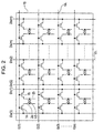
- FIG. 2 is a diagram showing an example of the configuration of pixels of a pixel unit of the liquid crystal device shown in FIG. 1 .
- FIG. 3 is a timing chart showing drive timings of a pixel according to an embodiment of the invention.
- FIGS. 4A and 4B are diagrams showing input-output characteristics (gray scale voltage levels with respect to input gray scale levels) of gray scale voltages which are supplied to one pair of pixel electrodes.
- FIG. 5 is a block diagram showing the configuration of a data line driving circuit (data line driving IC) according to a first embodiment of the invention.
- FIG. 6 is a diagram showing an example of an electro-optical characteristic of a liquid crystal.
- FIG. 7 is a circuit diagram showing a basic configuration of a gray scale voltage generating circuit for higher bits according to an embodiment of the invention.
- FIG. 8 is a circuit diagram showing a basic configuration of a gray scale voltage generating circuit for lower bits according to an embodiment of the invention.
- FIG. 9 is a circuit diagram showing the internal configuration of an output circuit disposed in a data line driving circuit according to an embodiment of the invention.
- FIG. 10 is a diagram showing another example (example in which a linear area is not included) of the electro-optical characteristic of a liquid crystal.
- FIG. 11 is a block diagram showing the configuration of a data line driving circuit (data line driving IC) according to a third embodiment of the invention.
- FIG. 12 is a diagram showing an example of the contents of a lookup table for ⁇ correction according to an embodiment of the invention.
- FIG. 13 is a diagram showing relationship between display gray scales and output voltage levels according to an embodiment of the invention.
- FIG. 14 is a diagram for showing cancel of feed-through by alternation in a method of driving a liquid crystal according to an embodiment of the invention.
- FIG. 15 is an example of the configuration of a known liquid crystal device in a case where 1024 gray scale levels are implemented.
- FIG. 16 is a diagram showing the whole configuration of a projector including an electro-optical device according to an embodiment of the invention.
- FIG. 17 is a perspective view showing the configuration of a personal computer including an electro-optical device according to an embodiment of the invention.
- FIG. 18 is a perspective view showing the configuration of a mobile terminal having a liquid crystal device according to an embodiment of the invention.
- a liquid crystal device has a pair of substrates disposed to face each other with a liquid crystal interposed therebetween. On a liquid crystal side of one substrate of the liquid crystal, scanning lines GL that extend in direction x and are disposed in direction y in parallel, and data line DL that extend in direction y and disposed in direction x in parallel are formed.
- Each scanning line GL is connected to a scanning line driving circuit 20 at least on its one end, and scanning line driving signals G( 1 ), G( 2 ), . . . , G(n) are configured to be sequentially supplied by the scanning line driving circuit 20 .
- Each data line DL is connected to a data line driving circuit 30 at least on its one end, and, for example image signals Da( 1 ), Db( 2 ), Da( 2 ), Db( 2 ), . . . , Da(m), Db(m), which are sequentially represented from the left side in the figure, are configured to be supplied in accordance with timings of supply of the scanning line driving signals G by the data line driving circuit 30 .
- a pixel is configured to be an area surrounded by a pair of adjacent scanning lines GL and a pair of adjacent data lines DL to which the image signals Da and Db are supplied, and aggregation of pixels is configured as a pixel unit 10 .
- the liquid crystal device has a configuration in which n scanning lines GL and 2m data lines DL are included for pixels in the shape of a matrix of n rows ⁇ m columns.
- the scanning line driving circuit 20 and the data line driving circuit 30 are configured to receive a scanning line driving control signal 21 and a data line driving control signal 31 from a timing control circuit 50 and output the scanning line driving signals G and the image signals Da and Db.
- a reference numeral 51 denotes an external input signal such as a power source or display data.
- FIG. 2 is a diagram showing an example of the configuration of pixels of the pixel unit of the liquid crystal device shown in FIG. 1 .
- TFT thin film transistors
- These thin film transistors 1 a and 1 b are implemented by MIS (metal insulator semiconductor) type transistors, and gate electrodes of the thin film transistors are connected to the scanning line GL.
- MIS metal insulator semiconductor
- one electrode (may be referred to as a drain electrode for the convenience of description) of electrodes other than the gate electrode of the thin film transistor 1 a is connected to a corresponding data line DL to which the image signal Da is supplied
- one electrode (may be referred to as a drain electrode for the convenience of description) of electrodes other than the gate electrode of the thin film transistor 1 b is connected to a corresponding data line DL to which the image signal Db is supplied.
- the TFTs 1 a and 1 b serving as a pair of transfer switches are included.
- the gates of the pair of TFTs 1 a and 1 b are connected to a common scanning line GL.
- one ends of the TFTs are connected to the data lines Da( 1 ) and Db( 1 ), and the other ends of the TFTs are connected to the pixel electrodes 2 a and 2 b of a liquid crystal LC.
- the liquid crystal LC is disposed between the pixel electrodes 2 a and 2 b .
- the alignment of molecules of the liquid crystal LC changes depending on an electric field generated due to a voltage difference between the pixel electrodes 2 a and 2 b , and thereby the light transmittance thereof changes.
- an image voltage corresponding to higher-bit image data of gray scale image data is applied to the pixel electrode 2 a
- an image voltage corresponding to lower-bit image data of the gray scale image data is applied to the pixel electrode 2 b (this aspect will be described later).
- the pixel electrodes 2 a and 2 b forming one pair are driven by two independent data lines (one pair of data lines), and the polarity of the gray scale voltage applied to each electrode is required to be inverted periodically.
- the structure of a pixel for inverting the polarity of the one pair of the liquid crystal electrodes 2 a and 2 b alternately can be easily implemented by using so-called a traversal field-type liquid crystal in which two electrodes 2 a and 2 b are disposed together on one substrate side (however, the present invention is not limited thereto).
- the traversal field-type liquid crystal includes an IPS (in-plane switching) liquid crystal. While an FFS (fringe field switching) liquid crystal is referred to as a fringing field switching liquid crystal or an oblique field liquid crystal, the FFS liquid crystal controls the alignment of liquid crystal molecules by using a traversal electric field, which is the same as the IPS liquid crystal. Thus, in descriptions here, the traversal electric field-type liquid crystal includes the FFS liquid crystal.
- FIG. 3 is a timing chart showing drive timings of a pixel.
- VST represents a start signal.
- VCK 1 and VCK 2 represent clock signals. These signals are included in a scanning line driving control signal 21 .
- the phases of scanning line driving signals G( 1 ), G( 2 ), G( 3 ), etc. are sequentially changed in synchronization with the clock signals VCK 1 and VCK 2 .
- the polarities thereof are shifted for each period of the start signal VST, and the signals are formed to be so-called “alternated”.
- the image signals Da and Db that is, the image signal of the higher bits and the image signal of the lower bits
- the image signals Da and Db are supplied to the electrodes 2 a and 2 b of the m-th row and n-th column pixel
- the image signals Da and Db are supplied to the electrodes 2 b and 2 a of a pixel of the (m+1)-th row and the n-th column pixel that is located next thereto.
- flicker can be reduced by inverting polarity for each adjacent pixel (dot).
- the pixel electrodes to which image signals Da(i) and Db(i) are supplied are shifted (that is, the polarities of the liquid crystals are shifted) for each horizontal period 1 H (that is, for each scanning line). In such a case, flicker can be reduced.
- FIGS. 4A and 4B are diagrams showing input-output characteristics (gray scale voltage levels with respect to input gray scale levels) of gray scale voltages Vda′(i) and Vdb′(i) corresponding to the higher bits and lower bits which are supplied to one pair of pixel electrodes.
- the gray scale voltages Vda′(i) and Vdb′(i) which are supplied to one pair of pixel electrodes may be referred to as one pair of recording voltages.
- FIG. 4A shows an input-output characteristic for positive polarity recording
- FIG. 4B shows an input-output output characteristic for negative polarity recording.
- a difference between gray scale voltages Vda′(i) and Vdb′(i) corresponding to the higher bits and the lower bits is a voltage level VLC applied to a liquid crystal (LC) of each pixel.
- LC liquid crystal
- FIG. 14 is a diagram for showing the advantage (an advantage acquired from reducing the effect of feed-through) acquired from alternating one pair of recording voltages Vda′(i) and Vdb′(i).
- the feed-through is a phenomenon that the voltage level applied to a liquid crystal (LC) varies as a variable voltage component is transmitted to the liquid crystal (LC) side through a parasitic capacitance by turning on/off the gate of a MOS transistor serving as a transfer switch.
- FIG. 14 voltage waveforms of image signals Da(i) and Db(i) applied to the pixel electrodes 2 a and 2 b in an actual driving state, a voltage waveform of a gate voltage (VGate) of a transfer switch (NMOS transistor), and voltage waveforms V( 2 a ) and V( 2 b ) representing temporal changes in substantial voltage levels applied to the pixel electrodes 2 a and 2 b are shown.
- V( 2 a ) and V( 2 b ) are represented by thick lines in the figure.
- VLC represented by a thick arrow is a voltage level VLC (a driving voltage level of the liquid crystal) applied between both ends of the liquid crystal.
- VLC a driving voltage level of the liquid crystal
- FIG. 5 is a block diagram showing the configuration of the data line driving circuit (data line driving IC).
- the data line driving circuit (data line driving IC) 30 has a control circuit 9 , two gray scale voltage generating circuits 21 a and 21 b , an input register 24 that latches image data of each color (RGB) transmitted from a data bus, a storage register 25 that temporarily stores image data of each color, a level shifter 26 , and an output circuit 27 .
- the control circuit 9 generates control signals based on input synchronization signals (a Vsync signal, an Hsync signal, and an enable signal ENA) and an operation clock CLK and controls other units by using the control signals.
- input synchronization signals a Vsync signal, an Hsync signal, and an enable signal ENA
- the input register 24 inserts 6-bit image data of each color corresponding to the number of outputs in synchronization with the operation clock CLK.
- the storage register 25 latches the image data, which has been transmitted from the input register 24 , in a parallel mode in synchronization with the operation clock CLK, similarly.
- the level of the image data latched by the storage register 25 is shifted by the level shifter 26 , and the image data is supplied to the output circuit 27 .
- the gray scale voltage generating circuits 21 a and 21 b respectively generate gray scale voltages corresponding to 64 gray scale levels based on three values of reference source voltages Vref 1 , Vref 2 , and Vref 3 .
- the gray scale voltage generating circuit 21 a generates gray scale voltage levels corresponding to the higher bits of the image data.
- the gray scale voltage generating circuit 21 b generates gray scale voltage levels corresponding to the lower bits of the image data.
- the gray scale voltage level may be referred to as a gradation voltage level.
- the gray scale voltage levels which have been generated by the gray scale voltage generating circuits 21 a and 21 b , corresponding to the higher bits and the lower bits are supplied to the output circuit 27 through voltage buses 28 a and 28 b.
- the output circuit 27 generates one pair of image signals Da(i) and Db(i) (that is, Da( 1 ) to Da(m) and Db( 1 ) to Db(m)) for each color (RGB) and outputs the image signals to the data lines DL.
- the image signals (gray scale voltage) output to the data lines DL are configured to have two series of Da(i) and Db(i) corresponding to one pair of data lines, and two gray scale voltage generating circuits 21 a and 21 b are disposed in correspondence with the two series of the image signals.
- FIG. 6 is a diagram showing an example of an electron optical characteristic of a liquid crystal.
- a data line driver 9 shown in FIG. 5 implements 64 gray scale levels by using a liquid crystal having the electro-optical characteristic shown in FIG. 6 .
- the liquid crystal shown in FIG. 6 has a region (a region corresponding to the liquid crystal driving voltage levels Voff to Von) in which light transmittance changes in a linear manner (in an ideally linear form) with respect to the driving voltage level VLC.
- a liquid crystal practically in use does not have such an ideally linear electro-optical characteristic, for the convenience of description of the principle operation of the liquid crystal according to an embodiment of the present invention, the liquid crystal having the electro-optical characteristic shown in FIG. 6 is considered.
- the data line driver 30 shown in FIG. 5 is configured to represent 64 gray scale levels by using the linear region (the region corresponding to the liquid crystal driving voltage levels Voff to Von) of the liquid crystal shown in FIG. 6 .
- the liquid crystal LC is driven by simultaneously applying a gray scale image signal corresponding to the higher bits and a gray scale image signal corresponding to the lower bits to both electrodes of the liquid crystal LC and using a difference between the voltage levels applied to the both electrodes.
- a bit division process is performed as below.
- image data having a 6-bit width is required.
- the image data is divided into higher 3 bits and lower 3 bits (however, the present invention is not limited thereto).
- Both the higher bits and the lower bits are respectively 3 bits, and thus 8 reference voltage levels (gray scale voltage levels) are required for each one of the higher bits and the lower bits, and a total of 16 reference voltage levels are required. Accordingly, the number of reference voltage levels can be configured to be 1 ⁇ 4 times “64” that is generally used.
- the 64 types of gray scale levels can be freely represented by selecting one from among a first reference voltage group and one from among a second reference voltage group and acquiring a difference therebetween.
- the voltage level selected from among the first reference voltage group is Da(i)
- the voltage level selected from among the second reference voltage group is Db(i).
- Db(i) is applied to the other electrode 2 b . Accordingly, a gray scale voltage level of “Da(i)-Db(i)” is applied to the liquid crystal LC, and transmittance corresponding to a wanted gray scale level can be implemented.
- the gray scale voltage level corresponding to the higher bits and the gray scale voltage level corresponding to the lower bits are required to be separately generated.
- FIG. 7 is a circuit diagram showing an example (using a ladder resistors) of the configuration of a gray scale voltage generating circuit for the higher bits according to an embodiment of the invention which generates a gray scale voltage level corresponding to the higher bits.
- FIG. 8 is a circuit diagram showing an example (using a ladder resistors) of the configuration of a gray scale voltage generating circuit for the lower bits according to an embodiment of the invention which generates a voltage level corresponding to the lower bits.
- the gray scale voltage generating circuit 21 a for the higher bits and the gray scale voltage generating circuit 21 b for the lower bits have ladder resistors having a configuration that a plurality of resistors are connected in series between reference voltages, and required gray scale voltage levels are generated by drawing out divided voltage levels from voltage divided points of the ladder resistors. Accordingly, simplification of the configuration of the circuit and effective generation of a plurality of gray scale voltage levels in a speedy manner can be made.
- One from among the plurality of the generated gray scale voltage levels is selected by a switching circuit.
- a switching circuit When an analog switch or the like is used as the switching circuit, a required gray scale voltage level can be precisely selected in a speedy manner (this aspect will be described later).
- a voltage-dividing resistor that is grounded is represented by R 3
- other voltage-dividing resistors are represented by R 2 . Accordingly, 8 gray scale voltage levels (VL 0 to VL 7 ) having equal electric potential differences are generated.
- Vref 3 is a voltage level corresponding to a difference (VH p ⁇ VH p-1 where p is one of 1 to 7) between the gray scale voltage level VH 0 to VH 7 for the higher bits which are shown in FIG. 7 and a voltage level of an adjacent gray scale voltage.
- the gray scale voltage generating circuit 21 b shown in FIG. 8 generates the gray scale voltage levels VL 0 to VL 7 having equal electric potential differences generated by equally dividing a distance between two reference voltage levels Vref 1 and Vref 2 by 56 (7 ⁇ 8).
- V ref1 ⁇ V ref2 8/9( V on ⁇ V off)
- V ref2 ⁇ V ref3 V off
- AF( 1 ) to AF( 3 ) denote buffers for supplying the reference source voltage levels Vref 1 to Vref 3 .
- BF 0 to BF 6 and KF 0 to KF 6 are ladder resistors or buffers for outputting acquired divided voltage levels. When additional current driving capability is not necessary, these buffers may not be used.
- FIG. 9 is a circuit diagram showing the circuit configuration of a part, which corresponds to one pixel, of an output circuit according to an embodiment of the invention which is disposed in the data line driving circuit.
- the output circuit 27 disposed in the data line driving circuit 30 selects and outputs one from among gray scale voltage levels VH 0 to VH 7 (Da(i)) of the first group and selects and outputs one from among gray scale voltage levels VL 7 to VL 0 (Db(i)) of the second group.
- the gray scale voltage levels VH 0 to VH 7 (Da(i)) of the first group are applied to lines L 0 to L 7
- the gray scale voltage levels VL 7 to VL 0 (Db(i)) of the first group are applied to lines L 10 to L 17 .
- a switch SW 1 having unit switches S 0 to S 7 is disposed.
- the unit switches S 0 to S 7 are appropriately switched in accordance with switch control signals Q 0 to Q 7 transmitted from the control circuit 9 .
- a switch SW 2 having unit switches ST 7 to ST 0 is disposed.
- the unit switches ST 7 to ST 0 are appropriately switched in accordance with switch control signals J 7 to J 0 transmitted from the control circuit 9 .
- the one selected from among the gray scale voltage levels VH 0 to VH 7 by the switch SW 1 is supplied to an output buffer AS 1 (may be omitted).
- the one selected from among the gray scale voltage levels VL 7 to VL 0 of the second group by the switch SW 2 is supplied to an output buffer AS 2 (may be omitted).
- a switch SW 3 and a switch SW 4 which are used for switching output paths are connected.
- the output buffers AS 1 and AS 2 may be disposed next to the switches SW 3 and SW 4 , and may be omitted in a case where current driving capability is not required.
- the relationships between Da(i) and Db(i) and the output buffers AS 1 and AS 2 are set to be opposite to each other in adjacent pixels.
- a total 18 of unit switches (8 switches of S 0 to S 7 , 8 switches of ST 0 to ST 7 , and 2 switches of SW 3 and SW 4 ) are used for each pixel.
- two output buffers AS 1 and AS 2 are used for each pixel (however, there is a case where the output buffers can be omitted).
- a total 16 of voltage buses VH 7 to VH 0 and VL 7 to VL 0 are wired along a long side thereof, and 18 ⁇ m (where m is the number of pixels in the scanning line direction) switches and 2 ⁇ m output buffers (may be omitted) are disposed.
- the reference voltage source Vref 3 may be set to be lower than the reference source voltage Vref 1 of the gray scale voltage generating circuit 21 a for the higher bits.
- transistors constituting the output buffer (AF( 3 ) shown in FIG. 8 ) of the gray scale voltage generating circuit 21 b may be configured by low withstand-voltage transistors. Accordingly, reduction of the size of the transistors (reduction of the area occupied by the IC) can be achieved.
- the transistors constituting the switches SW 2 (ST 0 to ST 7 ) shown in FIG. 9 and the output buffer AS 2 can be configured by low withstand-voltage transistors. Thereby, reduction of the size of the transistors (reduction of the area occupied by the IC) can be achieved.
- the source voltage level of the output buffer AS 2 can be lowered. Thereby, it is possible to reduce power consumption thereof.
- the gray scale voltage generating circuit 21 a for the higher bits and the gray scale voltage generating circuit 21 b for the lower bits can be configured to be equivalent circuits.
- the numbers of higher-bit unit switches S 0 to S 7 and lower-bit unit switches ST 0 to ST 7 , disposed in the output circuit 27 , which are used for selecting one from among the plurality of gray scale voltage levels become the same, the configuration of the circuit becomes symmetrical, and thereby it becomes easy to implement the most compact layout of the circuit.
- Z is acquired from calculating the square root of the number of gray scale levels.
- Z is the gray scale range of the lower bits, and the gray scale range for the higher bits becomes “Z 2 ⁇ Z”.
- the gray scale range for the lower bits is also Z-divided, and accordingly, Z gray scale voltages (reference voltages) output by the gray scale voltage generating circuit 21 b for the lower bits are determined.
- the gray scale range for the higher bits is also (Z ⁇ 1)-divided, and accordingly, Z gray scale voltages output by the gray scale voltage generating circuit 21 a for the higher bits are determined.
- the data line driving circuit 30 shown in FIG. 1 When the total number of bits of the gray scale data is even (that is, 2k bits (where k is a natural number equal to or larger than one)) and an equal-bit dividing method (a method in which the gray scale data is divided into k bits each) is used, the data line driving circuit 30 shown in FIG. 1 generates 2 k gray scale voltages VH 0 to VH 2 k ⁇ 1 (Da(i)), which have equal voltage differences, corresponding to the higher bits by (2 k ⁇ 1) dividing voltages corresponding to the gray scale range determined by the k higher bits.
- the data line driving circuit 30 selectively turns on one from among 2 k switches S 0 to S 2 k ⁇ 1 disposed in correspondence with the gray scale voltages VH 0 to VH 2 k ⁇ 1 (Da(i)) for the higher bits and supplies the selected gray scale voltage VH 0 to VH 2 k ⁇ 1 (Da(i)) for the higher bits to the first data line or the second data line.
- the data line driving circuit 30 selectively turns on one from among 2 k switches ST 0 to ST 2 k ⁇ 1 disposed in correspondence with the gray scale voltages VL 0 to VL 2 k ⁇ 1 (Db(i)) for the lower bits and supplies the selected gray scale voltage VL 0 to VL 2 k ⁇ 1 (Db(i)) for the lower bits to the second data line or the first data line.
- the gray scale data is divided into k higher bits and “k ⁇ 1” lower bits, In addition, it is preferable that the gray scale data is divided into “k ⁇ 1” higher bits and k lower bits.
- the numbers of selection switches for the higher bits and the lower bits can be minimized.
- a difference between the numbers of switches is also minimized, it becomes easy to dispose the switches with high density, and therefore there is an advantage for layout.
- the data line driving circuit 30 when the gray scale data is divided into k higher bits and “k ⁇ 1” lower bits, the data line driving circuit 30 generates 2 k gray scale voltages VH 0 to VH 2 k ⁇ 1 (Da(i)), which have equal voltage differences therebetween, corresponding to the higher bits by 2 k ⁇ 1 dividing the voltage level corresponding to the gray scale range determined by k higher bits.
- the data line driving circuit 30 selectively turns on one from among 2 k switches S 0 to S (2 k ⁇ 1) disposed in correspondence with the gray scale voltages VH 0 to VH 2 k ⁇ 1 (Da(i)) for the higher bits and supplies the selected gray scale voltage VH 0 to VL (2 k ⁇ 1) (Da(i)) for the higher bits to the first data line or the second data line.
- the data line driving circuit 30 selectively turns on one from among 2 (k-1) switches ST 0 to ST (2 (k-1) ⁇ 1) disposed in correspondence with the gray scale voltages VL 0 to VL (2 (k-1) ⁇ 1) (Db(i)) for the lower bits and supplies the selected gray scale voltage VL 0 to VL (2 (k-1) ⁇ 1) (Db(i)) for the lower bits to the second data line or the first data line.
- the data line driving circuit 30 when the gray scale data is divided into “k ⁇ 1” higher bits and k lower bits, the data line driving circuit 30 generates (2 (k-1) ⁇ 1) gray scale voltages VH 0 to VH (2 (k-1) ⁇ 1) (Da(i)), which have equal voltage differences therebetween, corresponding to the higher bits by 2 (k-1 ) ⁇ 1 dividing the voltage level corresponding to the gray scale range determined by “k ⁇ 1” higher bits.
- the data line driving circuit 30 selectively turns on one from among 2 (k-1) switches S 0 to S 2 (k-1) ⁇ 1) disposed in correspondence with the gray scale voltages VH 0 to VH (2 (k-1) ⁇ 1) (Da(i)) for the higher bits and supplies the selected gray scale voltage VH 0 to VH (2 (k-1) ⁇ 1) (Da(i)) for the higher bits to the first data line or the second data line.
- the data line driving circuit 30 selectively turns on one from among 2 k switches ST 0 to ST (2 k ⁇ 1) disposed in correspondence with the gray scale voltages VL 0 to VL (2 k ⁇ 1) (Da(i)) for the lower bits and supplies the selected gray scale voltage VL 0 to VL (2 k ⁇ 1) (Db(i)) for the lower bits to the second data line or the first data line.
- liquid crystal has been described to have an ideally linear property in the first embodiment, it is difficult for the electro-optical characteristic of a practical liquid crystal to be linear.
- frame rate control (FRC: a method of representing the number of colors which is larger than an actual displayable number of colors) may be considered to be used.
- FRC frame rate control
- the scale of the data line driving circuit 30 does not increase so much.
- a liquid crystal having the non-linear electro-optical characteristic as shown in FIG. 10 will be considered.
- the relationship between the output voltage and the display gray scale data in the data line driving circuit 30 is required to have a characteristic opposite to that of the liquid crystal.
- FIG. 11 is a block diagram showing the configuration of a data line driving circuit of an active matrix-type liquid crystal device according to a third embodiment of the invention.
- a same reference number is attached in the data line driving circuit 30 shown in FIG. 11 .
- lookup tables and decoders for each color of RGB are included in addition to the configuration shown in FIG. 5 .
- image data of 256 gray scale levels for each color of RGB is mapped into 1024 levels.
- gray scale voltages (having same electric potential differences) corresponding to the substantial 1024 gray scale levels are individually generated by the gray scale voltage generating circuit 21 a responsible for the higher bits and the gray scale voltage generating circuit 21 b responsible for the lower bits, and the gray scale voltages are applied to the pixel electrodes 2 a and 2 b of each pixel, and desired gray scale display is implemented by using a difference (a difference voltage level between the gray scale voltages corresponding to the higher bits and the lower bits) of the voltages applied to the electrodes.
- the number of the gray scale levels after the gray scale conversion process is 1024 (10 th power of 2) and 10-bit image data is formed. Accordingly, the image data is equally divided into the higher bits and the lower bits, and image data each having 5 bits is formed.
- the gray scale voltage generating circuit 21 a for the higher bits 31 ( 32 ⁇ 1)-divides the source voltage corresponding to the range of the 992 gray scale levels and generates 32 gray scale voltages for 32 higher bits.
- the number of the level shift circuits becomes “64 ⁇ m”.
- the number of the switches of the output circuit 27 for each pixel becomes 66 (32 ⁇ 2+2).
- the total number of the switches becomes “66 ⁇ m”.
- FIG. 15 The configuration of a known liquid crystal device is shown in FIG. 15 .
- 1024 voltage buses, “1024 ⁇ m” switches, 3 series of lookup tables each having 256 bits ⁇ 10 bits, 1024 ⁇ m level shifters are required, and thus a very large-scaled circuit is needed.
- the data line driving circuit 30 can be constituted by 64 voltage buses, “66 ⁇ m” switches, 3 series of lookup tables each having 256 bits ⁇ 10 bits, and “64 ⁇ m” level shifters. Accordingly, the configuration of the circuit can be markedly simplified.
- the decoder DER is disposed between the storage register 25 and the level shifter 26 , however, the present invention is not limited thereto. Thus, the decoder may be disposed between the input register 24 and the storage register 25 or between the level shifter 26 and the output circuit 27 .
- a polarity difference can be corrected by disposing an adder prior to a previous decoder and adding or not adding a value according to the polarity.
- FIG. 16 is a diagram showing the whole configuration of a projector including an electro-optical device (reflection-type liquid crystal device) according to an embodiment of the invention.
- a polarized lighting device 1110 is disposed along the optical axis PL of the system.
- light emitted from a lamp 1112 becomes light fluxes substantially parallel to one another due to reflection of a reflector 1114 , and the light fluxes are incident to a first integrator lens 1120 . Accordingly, the light emitted from the lamp 1112 is divided into a plurality of intermediate light fluxes.
- These divided intermediate light fluxes are converted into one type of polarized light fluxes (s polarized light fluxes) having a substantially-constant polarized direction by a polarization conversion element 1130 having a second integrator lens disposed on the light incident side and are emitted from the polarized lighting device 1110 .
- the s-polarized light fluxes emitted from the polarized lighting device 1110 are reflected by an s-polarized light flux reflecting surface 1141 of a polarization beam splitter 1140 .
- light fluxes of blue light B are reflected by a blue light reflecting layer of a dichroic mirror 1151 and are modulated by a reflection-type electro-optical device 100 B.
- light fluxes of red light R are reflected by a red light reflecting layer of a dichroic mirror 1152 and are modulated by a reflection-type electro-optical device 100 R.
- light fluxes of green light G are transmitted through the red light reflecting layer and are modulated by a reflection-type electro-optical device 100 G.
- the light fluxes of the red light, the green light, and the blue light modulated by the electro-optical devices 100 R, 100 G, and 100 B are sequentially composed by the dichroic mirrors 1152 and 1151 and the polarization beam splitter 1140 and are projected on a screen 1170 by a projection optical system 1160 . Since light fluxes corresponding to the original colors of R, G, and B are incident to the electro-optical devices 100 R, 100 B, and 100 G by the dichroic mirrors 1151 and 1152 , a color filter is not needed.
- the liquid crystal device according to an embodiment of the invention is configured to be simplified and miniaturized and is configured to have low power consumption and low cost, the same advantages as those of the liquid crystal device can be acquired by using the projector shown in FIG. 16 , and accordingly, the projector is useful as a projector for a home theater.
- the projector may use one between a reflection-type liquid crystal device and a liquid crystal device for projection-type display.
- FIG. 17 is a perspective view showing the configuration of a personal computer including an electro-optical device according to an embodiment of the invention.
- a computer 1200 is constituted by a main unit 1204 having a keyboard 1201 and a display unit 1206 .
- This display unit 1206 is configured by adding a front light on a front side of the above-described electro-optical device 100 .
- the electro-optical device 100 is used as a reflection direct-view type, it is preferable that concaves and convexes are formed in pixel electrodes 118 for scattering reflected light in various directions.
- the liquid crystal device according to an embodiment of the invention is configured to be simplified and miniaturized and is configured to have low power consumption and low cost, the same advantages as those of the liquid crystal device can be acquired by using the mobile computer shown in FIG. 17 .
- the liquid crystal device since the liquid crystal device has a superior characteristic for low power consumption, there is an advantage that the durability of a battery can be improved.
- FIG. 18 is a perspective view showing the configuration of a mobile terminal (here, a mobile phone) having a liquid crystal device according to an embodiment of the invention.
- the mobile phone 1300 has the electro-optical device 100 in addition to a plurality of operation buttons 1302 , an earpiece 1304 , and a mouthpiece 1305 .
- a front light is disposed as is needed.
- the electro-optical device 100 is used as a reflection direct-view type, it is preferable that concaves and convexes are formed in pixel electrodes 118 for scattering reflected light in various directions.
- the liquid crystal device according to an embodiment of the invention is configured to be simplified and miniaturized and is configured to have low power consumption and low cost, the same advantages as those of the liquid crystal device can be acquired by using the mobile terminal shown in FIG. 18 .
- the present invention may be applied to other electronic devices (for example, a liquid crystal television set, a view finder-type or a monitor direct view-type video cassette recorder, a car navigation system, a pager, an electronic diary, a calculator, a word processor, a workstation, a video phone, a POS terminal, a device having a touch panel, or the like).
- a compact and low-cost liquid crystal device capable of high precision display (multiple gray scale level display) can be acquired.
- the number of required electric potential-levels can be remarkably reduced by dividing the gray scale data into higher bits and lower bits and applying the gray scale data to each pixel electrode as a difference between two data lines, and thereby the configuration of the data line driving circuit can be simplified.
- variable range dynamic range
- the gray scale voltages on the lower bit side since a variable range (dynamic range) of the gray scale voltages on the lower bit side is small, low withstand-voltage elements can be used in a circuit relating to generation of the gray scale voltages on the lower bit side, and the circuit can be operated at a low source voltage level. Therefore, miniaturization, low power consumption, and low cost of the data line driving circuit (and the liquid crystal device) can be achieved.
- the present invention is the most appropriate for use as a mobile terminal or the like which requires miniaturization, light weight, and low cost.
- the technical idea of the invention may be applied to different electro-optical apparatuses.
- the present invention may be appropriately applied to a liquid crystal device, a driving circuit of a liquid crystal device, a method of driving a liquid crystal device, and an electronic apparatus.
Landscapes
- Engineering & Computer Science (AREA)
- Chemical & Material Sciences (AREA)
- Crystallography & Structural Chemistry (AREA)
- Physics & Mathematics (AREA)
- Computer Hardware Design (AREA)
- General Physics & Mathematics (AREA)
- Theoretical Computer Science (AREA)
- Control Of Indicators Other Than Cathode Ray Tubes (AREA)
- Liquid Crystal (AREA)
- Liquid Crystal Display Device Control (AREA)
Abstract
Description
(Vref1−Vref2)=8/9(Von−Voff)
(Vref2−Vref3)=Voff
Claims (16)
Applications Claiming Priority (2)
| Application Number | Priority Date | Filing Date | Title |
|---|---|---|---|
| JP2007093098A JP2008250118A (en) | 2007-03-30 | 2007-03-30 | Liquid crystal device, drive circuit of liquid crystal device, drive method of liquid crystal device, and electronic equipment |
| JP2007-093098 | 2007-03-30 |
Publications (2)
| Publication Number | Publication Date |
|---|---|
| US20080238842A1 US20080238842A1 (en) | 2008-10-02 |
| US8102343B2 true US8102343B2 (en) | 2012-01-24 |
Family
ID=39793415
Family Applications (1)
| Application Number | Title | Priority Date | Filing Date |
|---|---|---|---|
| US12/039,299 Active 2030-11-25 US8102343B2 (en) | 2007-03-30 | 2008-02-28 | Liquid crystal device, driving circuit for liquid crystal device, method of driving liquid crystal device, and electronic apparatus |
Country Status (3)
| Country | Link |
|---|---|
| US (1) | US8102343B2 (en) |
| JP (1) | JP2008250118A (en) |
| CN (1) | CN101276563A (en) |
Cited By (24)
| Publication number | Priority date | Publication date | Assignee | Title |
|---|---|---|---|---|
| US8994617B2 (en) | 2010-03-17 | 2015-03-31 | Ignis Innovation Inc. | Lifetime uniformity parameter extraction methods |
| US9330598B2 (en) | 2005-06-08 | 2016-05-03 | Ignis Innovation Inc. | Method and system for driving a light emitting device display |
| US9351368B2 (en) | 2013-03-08 | 2016-05-24 | Ignis Innovation Inc. | Pixel circuits for AMOLED displays |
| US9489891B2 (en) | 2006-01-09 | 2016-11-08 | Ignis Innovation Inc. | Method and system for driving an active matrix display circuit |
| US9697771B2 (en) | 2013-03-08 | 2017-07-04 | Ignis Innovation Inc. | Pixel circuits for AMOLED displays |
| US9721505B2 (en) | 2013-03-08 | 2017-08-01 | Ignis Innovation Inc. | Pixel circuits for AMOLED displays |
| US9741292B2 (en) | 2004-12-07 | 2017-08-22 | Ignis Innovation Inc. | Method and system for programming and driving active matrix light emitting device pixel having a controllable supply voltage |
| USRE46561E1 (en) | 2008-07-29 | 2017-09-26 | Ignis Innovation Inc. | Method and system for driving light emitting display |
| US9824632B2 (en) | 2008-12-09 | 2017-11-21 | Ignis Innovation Inc. | Systems and method for fast compensation programming of pixels in a display |
| US9867257B2 (en) | 2008-04-18 | 2018-01-09 | Ignis Innovation Inc. | System and driving method for light emitting device display |
| US9886899B2 (en) | 2011-05-17 | 2018-02-06 | Ignis Innovation Inc. | Pixel Circuits for AMOLED displays |
| US9978310B2 (en) | 2012-12-11 | 2018-05-22 | Ignis Innovation Inc. | Pixel circuits for amoled displays |
| US9997106B2 (en) | 2012-12-11 | 2018-06-12 | Ignis Innovation Inc. | Pixel circuits for AMOLED displays |
| US10102808B2 (en) | 2015-10-14 | 2018-10-16 | Ignis Innovation Inc. | Systems and methods of multiple color driving |
| US10134325B2 (en) | 2014-12-08 | 2018-11-20 | Ignis Innovation Inc. | Integrated display system |
| US10152915B2 (en) | 2015-04-01 | 2018-12-11 | Ignis Innovation Inc. | Systems and methods of display brightness adjustment |
| US10229647B2 (en) | 2006-01-09 | 2019-03-12 | Ignis Innovation Inc. | Method and system for driving an active matrix display circuit |
| US10242619B2 (en) | 2013-03-08 | 2019-03-26 | Ignis Innovation Inc. | Pixel circuits for amoled displays |
| US10290284B2 (en) | 2011-05-28 | 2019-05-14 | Ignis Innovation Inc. | Systems and methods for operating pixels in a display to mitigate image flicker |
| US10373554B2 (en) | 2015-07-24 | 2019-08-06 | Ignis Innovation Inc. | Pixels and reference circuits and timing techniques |
| US10410579B2 (en) | 2015-07-24 | 2019-09-10 | Ignis Innovation Inc. | Systems and methods of hybrid calibration of bias current |
| US10424245B2 (en) | 2012-05-11 | 2019-09-24 | Ignis Innovation Inc. | Pixel circuits including feedback capacitors and reset capacitors, and display systems therefore |
| US10657895B2 (en) | 2015-07-24 | 2020-05-19 | Ignis Innovation Inc. | Pixels and reference circuits and timing techniques |
| US11360363B2 (en) | 2018-01-19 | 2022-06-14 | Semiconductor Energy Laboratory Co., Ltd. | Display apparatus having pixels connected to first and second wirings set to different potentials |
Families Citing this family (9)
| Publication number | Priority date | Publication date | Assignee | Title |
|---|---|---|---|---|
| US8760479B2 (en) * | 2008-06-16 | 2014-06-24 | Samsung Display Co., Ltd. | Liquid crystal display |
| JP2010020730A (en) * | 2008-07-14 | 2010-01-28 | Fujitsu Component Ltd | Input detection circuit, input detection method, input detection program, and input detection apparatus |
| JP2010160373A (en) * | 2009-01-09 | 2010-07-22 | Renesas Technology Corp | Display drive device and display device |
| US20110298774A1 (en) * | 2009-03-18 | 2011-12-08 | Sharp Kabushiki Kaisha | Display apparatus |
| EP2299427A1 (en) * | 2009-09-09 | 2011-03-23 | Ignis Innovation Inc. | Driving System for Active-Matrix Displays |
| JP5691758B2 (en) * | 2011-04-06 | 2015-04-01 | 株式会社Jvcケンウッド | Liquid crystal display device and driving method thereof |
| TWI475552B (en) * | 2012-11-23 | 2015-03-01 | Au Optronics Corp | Pixel driving circuit |
| CN111417895B (en) * | 2017-12-22 | 2023-06-16 | 株式会社半导体能源研究所 | Display device |
| US10930234B1 (en) * | 2020-02-28 | 2021-02-23 | A.U. Vista, Inc. | Gray scale liquid crystal display panel with multiplexed analog gray levels |
Citations (3)
| Publication number | Priority date | Publication date | Assignee | Title |
|---|---|---|---|---|
| JPH09198012A (en) | 1996-01-24 | 1997-07-31 | Hitachi Ltd | Liquid crystal display device |
| JP2003302942A (en) | 2002-04-09 | 2003-10-24 | Hitachi Displays Ltd | Picture display |
| US7760179B2 (en) * | 2006-06-29 | 2010-07-20 | Lg Display Co., Ltd. | Liquid crystal panel having the dual data lines, data driver, liquid crystal display device having the same and driving method thereof |
Family Cites Families (4)
| Publication number | Priority date | Publication date | Assignee | Title |
|---|---|---|---|---|
| JPH0594154A (en) * | 1991-10-03 | 1993-04-16 | Fuji Electric Co Ltd | Liquid crystal display panel device |
| JP4014955B2 (en) * | 2002-07-10 | 2007-11-28 | 三菱電機株式会社 | Liquid crystal display |
| TWI251110B (en) * | 2003-12-18 | 2006-03-11 | Sharp Kk | Display device |
| JP4720261B2 (en) * | 2005-04-07 | 2011-07-13 | エプソンイメージングデバイス株式会社 | Electro-optical device, driving method, and electronic apparatus |
-
2007
- 2007-03-30 JP JP2007093098A patent/JP2008250118A/en not_active Withdrawn
-
2008
- 2008-02-28 US US12/039,299 patent/US8102343B2/en active Active
- 2008-03-26 CN CN200810087867.XA patent/CN101276563A/en active Pending
Patent Citations (3)
| Publication number | Priority date | Publication date | Assignee | Title |
|---|---|---|---|---|
| JPH09198012A (en) | 1996-01-24 | 1997-07-31 | Hitachi Ltd | Liquid crystal display device |
| JP2003302942A (en) | 2002-04-09 | 2003-10-24 | Hitachi Displays Ltd | Picture display |
| US7760179B2 (en) * | 2006-06-29 | 2010-07-20 | Lg Display Co., Ltd. | Liquid crystal panel having the dual data lines, data driver, liquid crystal display device having the same and driving method thereof |
Cited By (40)
| Publication number | Priority date | Publication date | Assignee | Title |
|---|---|---|---|---|
| US9741292B2 (en) | 2004-12-07 | 2017-08-22 | Ignis Innovation Inc. | Method and system for programming and driving active matrix light emitting device pixel having a controllable supply voltage |
| US9330598B2 (en) | 2005-06-08 | 2016-05-03 | Ignis Innovation Inc. | Method and system for driving a light emitting device display |
| US10388221B2 (en) | 2005-06-08 | 2019-08-20 | Ignis Innovation Inc. | Method and system for driving a light emitting device display |
| US9805653B2 (en) | 2005-06-08 | 2017-10-31 | Ignis Innovation Inc. | Method and system for driving a light emitting device display |
| US9489891B2 (en) | 2006-01-09 | 2016-11-08 | Ignis Innovation Inc. | Method and system for driving an active matrix display circuit |
| US10262587B2 (en) | 2006-01-09 | 2019-04-16 | Ignis Innovation Inc. | Method and system for driving an active matrix display circuit |
| US10229647B2 (en) | 2006-01-09 | 2019-03-12 | Ignis Innovation Inc. | Method and system for driving an active matrix display circuit |
| US10555398B2 (en) | 2008-04-18 | 2020-02-04 | Ignis Innovation Inc. | System and driving method for light emitting device display |
| US9867257B2 (en) | 2008-04-18 | 2018-01-09 | Ignis Innovation Inc. | System and driving method for light emitting device display |
| USRE46561E1 (en) | 2008-07-29 | 2017-09-26 | Ignis Innovation Inc. | Method and system for driving light emitting display |
| USRE49389E1 (en) | 2008-07-29 | 2023-01-24 | Ignis Innovation Inc. | Method and system for driving light emitting display |
| US11030949B2 (en) | 2008-12-09 | 2021-06-08 | Ignis Innovation Inc. | Systems and method for fast compensation programming of pixels in a display |
| US10134335B2 (en) | 2008-12-09 | 2018-11-20 | Ignis Innovation Inc. | Systems and method for fast compensation programming of pixels in a display |
| US9824632B2 (en) | 2008-12-09 | 2017-11-21 | Ignis Innovation Inc. | Systems and method for fast compensation programming of pixels in a display |
| US8994617B2 (en) | 2010-03-17 | 2015-03-31 | Ignis Innovation Inc. | Lifetime uniformity parameter extraction methods |
| US10515585B2 (en) | 2011-05-17 | 2019-12-24 | Ignis Innovation Inc. | Pixel circuits for AMOLED displays |
| US9886899B2 (en) | 2011-05-17 | 2018-02-06 | Ignis Innovation Inc. | Pixel Circuits for AMOLED displays |
| US10290284B2 (en) | 2011-05-28 | 2019-05-14 | Ignis Innovation Inc. | Systems and methods for operating pixels in a display to mitigate image flicker |
| US10424245B2 (en) | 2012-05-11 | 2019-09-24 | Ignis Innovation Inc. | Pixel circuits including feedback capacitors and reset capacitors, and display systems therefore |
| US11030955B2 (en) | 2012-12-11 | 2021-06-08 | Ignis Innovation Inc. | Pixel circuits for AMOLED displays |
| US9997106B2 (en) | 2012-12-11 | 2018-06-12 | Ignis Innovation Inc. | Pixel circuits for AMOLED displays |
| US9978310B2 (en) | 2012-12-11 | 2018-05-22 | Ignis Innovation Inc. | Pixel circuits for amoled displays |
| US10242619B2 (en) | 2013-03-08 | 2019-03-26 | Ignis Innovation Inc. | Pixel circuits for amoled displays |
| US9659527B2 (en) | 2013-03-08 | 2017-05-23 | Ignis Innovation Inc. | Pixel circuits for AMOLED displays |
| US10013915B2 (en) | 2013-03-08 | 2018-07-03 | Ignis Innovation Inc. | Pixel circuits for AMOLED displays |
| US9351368B2 (en) | 2013-03-08 | 2016-05-24 | Ignis Innovation Inc. | Pixel circuits for AMOLED displays |
| US9922596B2 (en) | 2013-03-08 | 2018-03-20 | Ignis Innovation Inc. | Pixel circuits for AMOLED displays |
| US10593263B2 (en) | 2013-03-08 | 2020-03-17 | Ignis Innovation Inc. | Pixel circuits for AMOLED displays |
| US9697771B2 (en) | 2013-03-08 | 2017-07-04 | Ignis Innovation Inc. | Pixel circuits for AMOLED displays |
| US9721505B2 (en) | 2013-03-08 | 2017-08-01 | Ignis Innovation Inc. | Pixel circuits for AMOLED displays |
| US10134325B2 (en) | 2014-12-08 | 2018-11-20 | Ignis Innovation Inc. | Integrated display system |
| US10726761B2 (en) | 2014-12-08 | 2020-07-28 | Ignis Innovation Inc. | Integrated display system |
| US10152915B2 (en) | 2015-04-01 | 2018-12-11 | Ignis Innovation Inc. | Systems and methods of display brightness adjustment |
| US10410579B2 (en) | 2015-07-24 | 2019-09-10 | Ignis Innovation Inc. | Systems and methods of hybrid calibration of bias current |
| US10657895B2 (en) | 2015-07-24 | 2020-05-19 | Ignis Innovation Inc. | Pixels and reference circuits and timing techniques |
| US10373554B2 (en) | 2015-07-24 | 2019-08-06 | Ignis Innovation Inc. | Pixels and reference circuits and timing techniques |
| US10446086B2 (en) | 2015-10-14 | 2019-10-15 | Ignis Innovation Inc. | Systems and methods of multiple color driving |
| US10102808B2 (en) | 2015-10-14 | 2018-10-16 | Ignis Innovation Inc. | Systems and methods of multiple color driving |
| US11360363B2 (en) | 2018-01-19 | 2022-06-14 | Semiconductor Energy Laboratory Co., Ltd. | Display apparatus having pixels connected to first and second wirings set to different potentials |
| US11815775B2 (en) | 2018-01-19 | 2023-11-14 | Semiconductor Energy Laboratory Co., Ltd. | Display apparatus having pixels connected to first and second wirings set to different potentials |
Also Published As
| Publication number | Publication date |
|---|---|
| CN101276563A (en) | 2008-10-01 |
| US20080238842A1 (en) | 2008-10-02 |
| JP2008250118A (en) | 2008-10-16 |
Similar Documents
| Publication | Publication Date | Title |
|---|---|---|
| US8102343B2 (en) | Liquid crystal device, driving circuit for liquid crystal device, method of driving liquid crystal device, and electronic apparatus | |
| US8139052B2 (en) | Electro-optical device, method of driving electro-optical device, and electronic apparatus | |
| JP3570362B2 (en) | Driving method of electro-optical device, image processing circuit, electro-optical device, and electronic apparatus | |
| JP3704715B2 (en) | Display device driving method, display device, and electronic apparatus using the same | |
| JP4786996B2 (en) | Display device | |
| JPH11272242A (en) | Digital driver circuit for electroptical device and electroptical device having the same | |
| JP5264048B2 (en) | Liquid crystal display device and driving method thereof | |
| US7705818B2 (en) | Electro-optical device, signal processing circuit thereof, signal processing method thereof and electronic apparatus | |
| KR20060065956A (en) | Liquid crystal display and driving apparatus of display device | |
| JP2010079151A (en) | Electrooptical apparatus, method for driving the same, and electronic device | |
| CN107808646B (en) | Display driver, electro-optical device, electronic apparatus, and method of controlling display driver | |
| JP2007206279A (en) | Liquid crystal display device | |
| US20080180374A1 (en) | Electro-optical device, processing circuit, processing method, and projector | |
| JP2001100707A (en) | Driving method of electrooptical device, driving circuit, electrooptical device and electronic equipment | |
| JP5023740B2 (en) | Electro-optical device, data signal supply circuit, supply method, and electronic apparatus | |
| JP6314432B2 (en) | Electro-optical device, driving method of electro-optical device, and electronic apparatus | |
| JPH11305743A (en) | Liquid crystal display device | |
| JP2007206621A (en) | Display driver and display device provided with the same | |
| JP2008299345A (en) | Display drive and display device | |
| JP2001221990A (en) | Driving circuit for electrooptical device, electrooptical device and electronic equipment | |
| JP3775137B2 (en) | Electro-optical device driving method, driving circuit, electro-optical device, and electronic apparatus | |
| JP2002169520A (en) | Electro-optical device, pattern generating circuit, and electronic equipment | |
| JP3598740B2 (en) | Drive circuit of liquid crystal display device, liquid crystal display device, and electronic equipment | |
| JP2006276119A (en) | Data signal supply circuit, supply method, opto-electronic apparatus and electronic apparatus | |
| JP5119901B2 (en) | Source driver, electro-optical device, projection display device, and electronic device |
Legal Events
| Date | Code | Title | Description |
|---|---|---|---|
| AS | Assignment |
Owner name: SEIKO EPSON CORPORATION, JAPAN Free format text: ASSIGNMENT OF ASSIGNORS INTEREST;ASSIGNOR:YATABE, SATOSHI;REEL/FRAME:020586/0352 Effective date: 20080220 |
|
| STCF | Information on status: patent grant |
Free format text: PATENTED CASE |
|
| FEPP | Fee payment procedure |
Free format text: PAYOR NUMBER ASSIGNED (ORIGINAL EVENT CODE: ASPN); ENTITY STATUS OF PATENT OWNER: LARGE ENTITY |
|
| FPAY | Fee payment |
Year of fee payment: 4 |
|
| AS | Assignment |
Owner name: BOE TECHNOLOGY GROUP CO., LTD., CHINA Free format text: ASSIGNMENT OF ASSIGNORS INTEREST;ASSIGNOR:BOE TECHNOLOGY (HK) LIMITED;REEL/FRAME:037515/0082 Effective date: 20150214 Owner name: BOE TECHNOLOGY (HK) LIMITED, CHINA Free format text: ASSIGNMENT OF ASSIGNORS INTEREST;ASSIGNOR:SEIKO EPSON CORPORATION;REEL/FRAME:037515/0050 Effective date: 20141118 |
|
| MAFP | Maintenance fee payment |
Free format text: PAYMENT OF MAINTENANCE FEE, 8TH YEAR, LARGE ENTITY (ORIGINAL EVENT CODE: M1552); ENTITY STATUS OF PATENT OWNER: LARGE ENTITY Year of fee payment: 8 |
|
| MAFP | Maintenance fee payment |
Free format text: PAYMENT OF MAINTENANCE FEE, 12TH YEAR, LARGE ENTITY (ORIGINAL EVENT CODE: M1553); ENTITY STATUS OF PATENT OWNER: LARGE ENTITY Year of fee payment: 12 |