US8084809B2 - Nonvolatile semiconductor memory device including pillars buried inside through holes - Google Patents
Nonvolatile semiconductor memory device including pillars buried inside through holes Download PDFInfo
- Publication number
- US8084809B2 US8084809B2 US12/408,183 US40818309A US8084809B2 US 8084809 B2 US8084809 B2 US 8084809B2 US 40818309 A US40818309 A US 40818309A US 8084809 B2 US8084809 B2 US 8084809B2
- Authority
- US
- United States
- Prior art keywords
- interconnect
- holes
- pillars
- semiconductor
- memory device
- Prior art date
- Legal status (The legal status is an assumption and is not a legal conclusion. Google has not performed a legal analysis and makes no representation as to the accuracy of the status listed.)
- Active, expires
Links
Images


Classifications
-
- H—ELECTRICITY
- H01—ELECTRIC ELEMENTS
- H01L—SEMICONDUCTOR DEVICES NOT COVERED BY CLASS H10
- H01L23/00—Details of semiconductor or other solid state devices
- H01L23/52—Arrangements for conducting electric current within the device in operation from one component to another, i.e. interconnections, e.g. wires, lead frames
- H01L23/522—Arrangements for conducting electric current within the device in operation from one component to another, i.e. interconnections, e.g. wires, lead frames including external interconnections consisting of a multilayer structure of conductive and insulating layers inseparably formed on the semiconductor body
- H01L23/528—Geometry or layout of the interconnection structure
-
- H—ELECTRICITY
- H01—ELECTRIC ELEMENTS
- H01L—SEMICONDUCTOR DEVICES NOT COVERED BY CLASS H10
- H01L23/00—Details of semiconductor or other solid state devices
- H01L23/52—Arrangements for conducting electric current within the device in operation from one component to another, i.e. interconnections, e.g. wires, lead frames
- H01L23/522—Arrangements for conducting electric current within the device in operation from one component to another, i.e. interconnections, e.g. wires, lead frames including external interconnections consisting of a multilayer structure of conductive and insulating layers inseparably formed on the semiconductor body
- H01L23/5226—Via connections in a multilevel interconnection structure
-
- H—ELECTRICITY
- H10—SEMICONDUCTOR DEVICES; ELECTRIC SOLID-STATE DEVICES NOT OTHERWISE PROVIDED FOR
- H10B—ELECTRONIC MEMORY DEVICES
- H10B41/00—Electrically erasable-and-programmable ROM [EEPROM] devices comprising floating gates
- H10B41/20—Electrically erasable-and-programmable ROM [EEPROM] devices comprising floating gates characterised by three-dimensional arrangements, e.g. with cells on different height levels
- H10B41/23—Electrically erasable-and-programmable ROM [EEPROM] devices comprising floating gates characterised by three-dimensional arrangements, e.g. with cells on different height levels with source and drain on different levels, e.g. with sloping channels
- H10B41/27—Electrically erasable-and-programmable ROM [EEPROM] devices comprising floating gates characterised by three-dimensional arrangements, e.g. with cells on different height levels with source and drain on different levels, e.g. with sloping channels the channels comprising vertical portions, e.g. U-shaped channels
-
- H—ELECTRICITY
- H10—SEMICONDUCTOR DEVICES; ELECTRIC SOLID-STATE DEVICES NOT OTHERWISE PROVIDED FOR
- H10B—ELECTRONIC MEMORY DEVICES
- H10B43/00—EEPROM devices comprising charge-trapping gate insulators
- H10B43/20—EEPROM devices comprising charge-trapping gate insulators characterised by three-dimensional arrangements, e.g. with cells on different height levels
- H10B43/23—EEPROM devices comprising charge-trapping gate insulators characterised by three-dimensional arrangements, e.g. with cells on different height levels with source and drain on different levels, e.g. with sloping channels
- H10B43/27—EEPROM devices comprising charge-trapping gate insulators characterised by three-dimensional arrangements, e.g. with cells on different height levels with source and drain on different levels, e.g. with sloping channels the channels comprising vertical portions, e.g. U-shaped channels
-
- H—ELECTRICITY
- H10—SEMICONDUCTOR DEVICES; ELECTRIC SOLID-STATE DEVICES NOT OTHERWISE PROVIDED FOR
- H10B—ELECTRONIC MEMORY DEVICES
- H10B43/00—EEPROM devices comprising charge-trapping gate insulators
- H10B43/30—EEPROM devices comprising charge-trapping gate insulators characterised by the memory core region
- H10B43/35—EEPROM devices comprising charge-trapping gate insulators characterised by the memory core region with cell select transistors, e.g. NAND
-
- H—ELECTRICITY
- H01—ELECTRIC ELEMENTS
- H01L—SEMICONDUCTOR DEVICES NOT COVERED BY CLASS H10
- H01L2924/00—Indexing scheme for arrangements or methods for connecting or disconnecting semiconductor or solid-state bodies as covered by H01L24/00
- H01L2924/0001—Technical content checked by a classifier
- H01L2924/0002—Not covered by any one of groups H01L24/00, H01L24/00 and H01L2224/00
Definitions
- This invention relates to a nonvolatile semiconductor memory device with a plurality of dielectric films and electrode films alternately stacked on a substrate, and a method for manufacturing the same.
- dielectric films and electrode films are alternately stacked on a substrate, and then through holes are simultaneously formed therein.
- a charge storage layer for retaining charge is formed on the inner surface of the through holes, and a columnar semiconductor pillar is buried inside each through hole.
- a memory cell is formed at each intersection between the semiconductor pillar and the electrode film.
- the uppermost electrode film is divided into a plurality of select gate lines extending in one direction, and a plurality of bit lines extending in another direction are provided above the electrode film and connected to the upper end portion of the semiconductor pillars, so that any of the semiconductor pillars can be selected.
- a diffusion region is formed in an upper portion of the substrate to serve as a source electrode connected to the lower end of the semiconductor pillars.
- a flash memory with memory cells three-dimensionally stacked can be fabricated (see, e.g., JP-A-2007-266143(Kokai)).
- the conductive portions are three-dimensionally arranged.
- the conductive portions located other than in the uppermost interconnect layer such as the diffusion region constituting the source electrode and the electrode film constituting the select gate line and the word line, can be supplied with an electric potential only through the respective end portions thereof.
- the aforementioned conductive portions are also upsized, unfortunately increasing the resistance. This makes it difficult to rapidly place each conductive portion at a desired potential, which results in increased time required for data write, read, and erase operation, and may cause malfunctions.
- division into a plurality of memory cell arrays may be contemplated. However, in this case, each memory cell array requires a row decoder and other circuits, which increases the chip area.
- a nonvolatile semiconductor memory device including: a substrate; a semiconductor region formed in an upper portion of the substrate; a plurality of dielectric films and electrode films which are alternately stacked on the substrate and have a plurality of through holes extending in the stacking direction and formed in a matrix configuration as viewed along the stacking direction; conductor pillars buried inside a subset of the plurality of through holes, the through holes in the subset being arranged in a first direction; semiconductor pillars buried inside the remaining through holes and connected to the semiconductor region; a shunt interconnect provided above the plurality of dielectric films and electrode films and connected to the conductor pillars; a bit interconnect provided above the plurality of dielectric films and electrode films and connected to the semiconductor pillars; and a charge storage layer provided at least between the semiconductor pillar and some of the electrode films, the conductor pillar having a lower resistivity than the semiconductor pillar.
- a method for manufacturing a nonvolatile semiconductor memory device including: doping an upper portion of a substrate with impurities to form a semiconductor region; forming one dielectric film and one electrode film on the substrate to form a lower stacked body; forming lower through holes in the lower stacked body in a matrix configuration; forming a gate dielectric film on an inner surface of the lower through holes; burying a semiconductor material inside the lower through holes; alternately stacking a plurality of dielectric films and a plurality of electrode films on the lower stacked body to form an intermediate stacked body; forming intermediate through holes in the intermediate stacked body immediately above the lower through holes; forming a charge storage layer on an inner surface of the intermediate through holes; burying a semiconductor material inside the intermediate through holes; forming one dielectric film, one electrode film, and one dielectric film in this order on the intermediate stacked body to form an upper stacked body; forming upper through holes in the upper stacked body immediately above the intermediate through holes; forming a
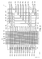
- FIG. 1 is a perspective view illustrating a nonvolatile semiconductor memory device according to a first embodiment of the invention
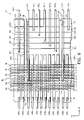
- FIG. 2 is a plan view illustrating the nonvolatile semiconductor memory device according to the first embodiment
- FIG. 3 is a cross-sectional view illustrating the nonvolatile semiconductor memory device according to the first embodiment
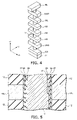
- FIG. 4 is a perspective view illustrating one memory string in the nonvolatile semiconductor memory device according to the first embodiment
- FIG. 5 is a cross-sectional view illustrating one memory cell in the nonvolatile semiconductor memory device according to the first embodiment
- FIG. 6 is a plan view illustrating a nonvolatile semiconductor memory device according to a second embodiment of the invention.
- FIG. 7 is a cross-sectional view illustrating the nonvolatile semiconductor memory device according to the second embodiment.
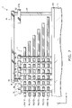
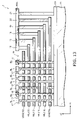
- FIG. 8 is a plan view illustrating a nonvolatile semiconductor memory device according to a third embodiment of the invention.
- FIG. 9 is a cross-sectional view illustrating a nonvolatile semiconductor memory device according to a fourth embodiment of the invention.
- FIG. 10 is a cross-sectional view illustrating a nonvolatile semiconductor memory device according to a fifth embodiment of the invention.
- FIG. 11 is a plan view illustrating a nonvolatile semiconductor memory device according to a sixth embodiment of the invention.
- FIG. 12 is a cross-sectional view illustrating the nonvolatile semiconductor memory device according to the sixth embodiment.
- FIG. 13 is a cross-sectional view illustrating a nonvolatile semiconductor memory device according to a seventh embodiment of the invention.
- FIG. 14 is a cross-sectional view illustrating a nonvolatile semiconductor memory device according to an eighth embodiment of the invention.
- FIG. 1 is a perspective view illustrating a nonvolatile semiconductor memory device according to this embodiment.
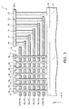
- FIG. 2 is a plan view illustrating the nonvolatile semiconductor memory device according to this embodiment.
- FIG. 3 is a cross-sectional view illustrating the nonvolatile semiconductor memory device according to this embodiment.
- FIG. 4 is a perspective view illustrating one memory string in the nonvolatile semiconductor memory device according to this embodiment.
- FIG. 5 is a cross-sectional view illustrating one memory cell in the nonvolatile semiconductor memory device according to this embodiment.
- FIGS. 1 to 4 for clarity of illustration, only the conductive portions are shown, and the dielectric portions are not shown. Furthermore, in FIGS. 1 and 2 , illustration of the silicon substrate 11 is also omitted. Similarly, in the other embodiments described later, the figures are simplified as appropriate.
- the nonvolatile semiconductor memory device 1 (hereinafter also simply referred to as “device 1 ”) according to this embodiment includes a silicon substrate 11 illustratively made of single crystal silicon.
- One memory cell array is provided in an upper portion of the silicon substrate 11 and thereabove.
- a rectangular region in the upper portion of the silicon substrate 11 is doped with impurities to form a semiconductor region serving as a cell source CS.
- a plurality of dielectric films 12 (see FIG. 5 ) illustratively made of silicon oxide (SiO 2 ) and a plurality of electrode films 13 illustratively made of polycrystalline silicon are alternately stacked to form a stacked body 14 .
- the thickness of the electrode film 13 is illustratively 50 nanometers (nm) or more, and the number of stacked layers is illustratively six.
- an XYZ orthogonal coordinate system is herein introduced.
- the two directions parallel to the upper surface of the silicon substrate 11 and orthogonal to each other are referred to as the X and Y direction
- the direction orthogonal to both the X and Y direction is referred to as the Z direction.
- the X-direction length of the electrode films 13 becomes shorter toward the upside. As viewed from above (+Z direction), each electrode film 13 is located inside the electrode films 13 and the cell source CS located therebelow. On the other hand, the electrode films 13 have the same Y-direction length. Dielectric films (not shown) are provided in the ⁇ X and ⁇ Y direction as viewed from the electrode film 13 .
- the lowermost electrode film 13 serves as a lower select gate LSG
- the uppermost electrode film 13 serves as an upper select gate USG
- the other electrode films 13 serve as word lines WL.
- the number of stacked electrode films 13 is illustratively six. Hence, sequentially from the top, the electrode films 13 serve as an upper select gate USG, four word lines WL, and a lower select gate LSG.
- the stacked body 14 is provided in a plurality along the Y direction.
- the upper select gate USG is divided along the Y direction into a plurality of interconnecting conductive members extending in the X direction.
- the word line WL and the lower select gate LSG are not divided in the individual stacked body 14 , but are each formed into one plate-like conductive member parallel to the XY plane.
- the cell source CS is also not divided, but is formed into one plate-like conductive member constituting the XY plane so as to connect the immediately underlying regions of the plurality of stacked bodies 14 .
- Each dielectric film 12 and each electrode film 13 include a plurality of through holes 15 extending in the stacking direction (Z direction).
- the through holes 15 are arranged in a matrix configuration along the X and Y direction, and the arrangement period of the through holes 15 is constant in each of the X and Y direction.
- Each through hole 15 penetrates entirely through the stacked body 14 .
- a plurality of through holes 15 are arranged in a line along the X direction.
- Conductor pillars 16 are buried in a subset of the plurality of through holes 15 arranged in a line in the Y direction.
- the conductor pillar 16 is formed from a metal such as tungsten (W) or aluminum (Al), or a semiconductor highly doped with impurities such as polycrystalline silicon or amorphous silicon. It is noted that the term “metal” used herein includes alloys as well as pure metals.
- semiconductor pillars 17 are buried in the remaining through holes 15 .
- the semiconductor pillar 17 is formed from a semiconductor doped with impurities such as polycrystalline silicon or amorphous silicon.
- the conductor pillar 16 has the same cylindrical shape as the semiconductor pillar 17 , both extending in the Z direction. In this embodiment, the lower end portions of the conductor pillar 16 and the semiconductor pillar 17 are both connected to the cell source CS.
- the conductor pillars 16 are located in the vicinity of the X-direction center portion in the matrix composed of the conductor pillars 16 and the semiconductor pillars 17 .
- the invention is not limited thereto.
- the conductor pillars 16 may be located at the ⁇ X-direction end portion of the matrix composed of the conductor pillars 16 and the semiconductor pillars 17 .
- a plurality of bit interconnects BL extending in the Y direction are provided immediately above the region including the upper select gate USG. Furthermore, one shunt interconnect SL, for example, is mixed with the bit interconnects BL.
- the bit interconnects BL and the shunt interconnect SL are located at an equal height and formed from a metal such as tungsten, aluminum, or copper (Cu).
- the shunt interconnect SL is provided immediately above the conductor pillars 16 and connected to the upper end portion of each conductor pillar 16 .
- the bit interconnects BL are provided immediately above the semiconductor pillars 17 , and each bit interconnect BL is connected to the upper end portion of each column of the semiconductor pillars 17 arranged along the Y direction.
- the semiconductor pillars 17 in different columns extending in the Y direction are connected to different bit interconnects BL.
- the bit interconnects BL and the shunt interconnect SL are continuously disposed so as to extend immediately above the plurality of stacked bodies 14 arranged in the Y direction, and commonly connected to the semiconductor pillars 17 and the conductor pillars 16 in the respective stacked bodies 14 .
- the conductor pillar 16 and the semiconductor pillar 17 have the same shape, and the lower end portions thereof are both connected to the cell source CS. However, these pillars have different functions.
- the conductor pillar 16 serves as a connecting member for connecting the shunt interconnect SL to the cell source CS.
- the semiconductor pillar 17 serves as a semiconductor region of the transistor constituting a memory cell in the portion where the semiconductor pillar 17 penetrates through the word line WL. Hence, the conductor pillar 16 has a lower resistivity than the semiconductor pillar 17 .
- a plurality of upper select gate interconnects USL extending in the X direction are provided on the ⁇ X-direction side of the region including the bit interconnects BL and the shunt interconnect SL.
- the upper select gate interconnect USL is formed from a metal such as tungsten, aluminum, or copper.
- the number of upper select gate interconnects USL is the same as the upper select gates USG, and each upper select gate interconnect USL is connected to a corresponding one of the upper select gates USG through a via 18 .
- a plurality of word interconnects WLL extending in the X direction, one lower select gate interconnect LSL extending in the X direction, and one cell source interconnect CSL extending in the X direction are provided.
- the word interconnect WLL, the lower select gate interconnect LSL, and the cell source interconnect CSL are formed from a metal such as tungsten, aluminum, or copper.
- the number of word interconnects WLL for each stacked body 14 is the same as the number of word lines WL, and each word interconnect WLL is connected to a corresponding one of the word lines WL through a via 19 .
- the lower select gate interconnect LSL is connected to the lower select gate LSG through a via 20
- the cell source interconnect CSL is connected to the cell source CS through a contact 21 .
- the vias 19 , 20 and the contact 21 are formed in a region immediately above the electrode film 13 to which they are connected, the region lying on the +X-direction side out of the overlying electrode film 13 .
- bit interconnect BL, the shunt interconnect SL, the upper select gate interconnect USL, the word interconnect WLL, the lower select gate interconnect LSL, and the cell source interconnect CSL are identical in the position along the height (Z direction), thickness, and material, and illustratively formed by patterning one metal film.
- the interconnects are insulated from each other by an interlayer dielectric film (not shown).
- each semiconductor pillar 17 is connected between a bit interconnect BL and the cell source CS, and penetrates through an upper select gate USG, a plurality of word lines WL, and the lower select gate LSG from above to below, that is, from the junction with the bit interconnect BL toward the junction with the cell source CS.
- a dielectric layer 25 , a charge storage layer 26 , and a dielectric layer 27 are laminated in this order from the inside, that is, from the semiconductor pillar 17 side.
- the dielectric layers 25 and 27 are illustratively made of silicon oxide (SiO 2 ), and the charge storage layer 26 is illustratively made of silicon nitride (SiN).
- an SGT serving as a memory cell is formed at the intersection between the semiconductor pillar 17 and the word line WL, and charge is stored in the portion of the charge storage layer 26 located in the SGT.
- a plurality of semiconductor pillars 17 are arranged in a matrix configuration along the X and Y direction.
- a plurality of memory cells are three-dimensionally arranged along the X, Y, and Z direction.
- a gate dielectric film (not shown) is provided in the cylindrical portion between the semiconductor pillar 17 and the upper select gate USG and between the semiconductor pillar 17 and the lower select gate LSG.
- SGTs are formed also at the intersection between the semiconductor pillar 17 and the upper select gate USG and at the intersection between the semiconductor pillar 17 and the lower select gate LSG, respectively. These SGTs do not serve as memory cells, but serve to select the semiconductor pillar 17 .
- a dielectric layer 25 , a charge storage layer 26 , and a dielectric layer 27 are laminated in this order.
- the conductor pillar 16 is insulated from the electrode film 13 , that is, from the upper select gate USG, the word line WL, and the lower select gate LSG, but connected only to the shunt interconnect SL and the cell source CS.
- at least one of the dielectric layers 25 and 27 only needs to be provided around the conductor pillar 16 , and the charge storage layer 26 may be omitted.
- a gate dielectric film (not shown) is provided between the conductor pillar 16 and the upper select gate USG and between the conductor pillar 16 and the lower select gate LSG.
- the charge storage layer 26 only needs to be provided at least between the semiconductor pillar 17 and part of the electrode film 13 , that is, in the portion constituting the memory cell.
- the device 1 further includes a driver circuit for applying a potential to the upper end portion of the semiconductor pillar 17 through the bit interconnect BL, a driver circuit for applying a potential to the lower end portion of the semiconductor pillar 17 through the cell source CS, a driver circuit for applying a potential to the upper select gate USG through the upper select gate interconnect USL, a driver circuit for applying a potential to the lower select gate LSG through the lower select gate interconnect LSL, and a driver circuit for applying a potential to each word line WL through the word interconnect WLL (all the driver circuits being not shown).
- a rectangular region in an upper portion of a silicon substrate 11 is doped with impurities to form a cell source CS.
- one dielectric film 12 and one electrode film 13 are formed on the silicon substrate 11 .
- through holes are formed in the lower stacked body composed of these electrode film 13 and dielectric film 12 .
- the through holes are simultaneously formed in a matrix configuration in the region where conductor pillars 16 are to be formed and the region where semiconductor pillars 17 are to be formed in the later process.
- a gate dielectric film is formed on the inner surface of the through hole, and a semiconductor material, such as N-type polycrystalline silicon or amorphous silicon doped with donors, is buried in the through holes.
- a lower select gate LSG, the lower portion of the through holes 15 , and the lower portion of the semiconductor pillars 17 are formed.
- a plurality of, e.g. four dielectric films 12 and e.g. four electrode films 13 are alternately stacked to form an intermediate stacked body.
- through holes are formed in the intermediate stacked body composed of the stacked electrode films 13 and dielectric films 12 .
- the through holes to be buried with conductor pillars 16 and the through holes to be buried with semiconductor pillars 17 in the later process are simultaneously formed in a matrix configuration. That is, new through holes are formed immediately above the previously formed through holes.
- a dielectric layer 27 , a charge storage layer 26 , and a dielectric layer 25 are formed in this order on the inner surface of the through hole.
- a semiconductor material such as N-type polycrystalline silicon or amorphous silicon doped with donors, is buried in all the through holes.
- the four electrode films 13 serve as word lines WL, and the center portion of the through holes 15 and the center portion of the semiconductor pillars 17 are formed.
- one dielectric film 12 , one electrode film 13 , and one dielectric film 12 are formed in this order to form an upper stacked body.
- new through holes are formed in the upper stacked body immediately above the through holes formed in the intermediate stacked body.
- a gate dielectric film is formed on the inner surface of the through hole, and a semiconductor material is buried therein.
- the formed electrode film 13 serves as an upper select gate USG, and the upper portion of the through holes 15 and the upper portion of the semiconductor pillars 17 are formed.
- the lower portion, the center portion, and the upper portion of the through hole 15 communicate with each other to form one through hole 15 .
- the lower portion, the center portion, and the upper portion of the semiconductor pillar 17 are connected to each other to form one semiconductor pillar 17 . Consequently, the through holes 15 and the semiconductor pillars 17 are completed.
- a resist film (not shown) is formed so as to expose only the through holes 15 to be buried with conductor pillars 16 while covering the other through holes 15 .
- This resist film is used as a mask to perform etching, thereby removing the semiconductor pillars 17 from inside the through holes 15 to be buried with conductor pillars 16 .
- a conductor material such as N + -type polycrystalline silicon or amorphous silicon doped with donors at a higher concentration than the conductor pillar 16 , or a metal such as tungsten or aluminum, is newly buried in these through holes 15 to form conductor pillars 16 .
- bit interconnects BL bit interconnects BL
- a shunt interconnect SL upper select gate interconnects USL
- word interconnects WLL word interconnects WLL
- a lower select gate interconnect LSL lower select gate interconnect LSL
- cell source interconnect CSL cell source interconnect
- the device 1 can be manufactured also by the following method.
- a resist film (not shown) is formed to cover the region where conductor pillars 16 are to be formed while exposing the region where semiconductor pillars 17 are to be formed.
- This resist film is used as a mask to perform etching so that only the through holes 15 to be buried with semiconductor pillars 17 are formed first.
- a semiconductor material is buried in these through holes 15 to form semiconductor pillars 17 .
- the stacked body 14 is formed, after that through holes 15 are formed in the region to be buried with conductors 16 , and a conductive material is buried therein to form conductor pillars 16 .
- bit interconnects BL, a shunt interconnect SL, upper select gate interconnects USL, word interconnects WLL, a lower select gate interconnect LSL, and a cell source interconnect CSL are formed.
- the X coordinate of a memory cell is selected by selecting a bit line BL
- the Y coordinate of the memory cell is selected by selecting an upper select gate USG
- the Z coordinate of the memory cell is selected by selecting a word line WL.
- one memory cell is selected from the device 1 , and data is stored or erased by charge injection into or extraction from this memory cell.
- the stored data is read by passing a sense current between the bit line BL and the cell source CS so that the sense current flows through this memory cell.
- the shunt interconnect SL is connected to the cell source CS through the conductor pillar 16 .
- the potential applied to the shunt interconnect SL can be applied to the cell source CS.
- the potential can be applied to the +X-direction end portion of the cell source CS through the cell source interconnect CSL and the contact 21 , and also to the X-direction center portion of the cell source CS through the shunt interconnect SL and the conductor pillar 16 . Consequently, even if the device 1 is upsized, the cell source CS can be rapidly charged/discharged, and its potential can be rapidly adjusted to a prescribed potential.
- the potential can be applied only through the end portion of the cell source CS when the potential of the cell source CS is adjusted to a prescribed potential.
- the cell source CS is an impurity diffusion layer formed in the upper portion of the silicon substrate 11 , it has a higher resistivity than the metal portion.
- the time required for adjusting the potential of the cell source CS to a prescribed potential is longer than in the case where the shunt interconnect SL and the conductor pillar 16 are provided.
- the memory cell array is upsized, the time required for each operation increases, and malfunctions are more likely to occur.
- a plurality of small memory cell arrays are needed. This results in increased peripheral circuits and chip area.
- conductor pillars 16 are buried in one column of the through holes 15 located at the X-direction center portion. Hence, the conductor pillars 16 can be connected to the X-direction center portion of the cell source CS.
- FIG. 6 is a plan view illustrating a nonvolatile semiconductor memory device according to this embodiment.
- FIG. 7 is a cross-sectional view illustrating the nonvolatile semiconductor memory device according to this embodiment.
- an upper interconnect M extending in the X direction is provided above the shunt interconnect SL.
- the upper interconnect M is disposed for each stacked body 14 from immediately above the cell source interconnect CSL to immediately above the shunt interconnect SL.
- the +X-direction end portion of the upper interconnect M is connected to the cell source interconnect CSL through a via 32
- the ⁇ X-direction end portion is connected to the shunt interconnect SL through a via 33 .
- the upper interconnect M is formed from a metal such as tungsten, aluminum, or copper.
- a driver circuit for the cell source is needed.
- the cell source interconnect CSL can be connected to the shunt interconnect SL through the upper interconnect M.
- the overall configuration of the device can be simplified, and the device can be further downsized.
- FIG. 8 is a plan view illustrating a nonvolatile semiconductor memory device according to this embodiment.
- the shunt interconnect SL is divided for each stacked body 14 .
- the upper interconnect M is provided for each stacked body 14 .
- the device 3 includes as many upper interconnects M as the stacked bodies 14 .
- the cell source CS is also divided for each stacked body 14 into a plurality of portions along the Y direction. The plurality of portions of the cell source CS are arranged along the Y direction, and electrically isolated from each other.
- the upper interconnect M is connected to the corresponding portion of the cell source CS through the shunt interconnect SL and the conductor pillar 16 .
- the configuration in this embodiment other than the foregoing is the same as that in the above second embodiment.
- the shunt interconnect SL and the cell source CS are divided for each stacked body 14 , and the upper interconnect M is provided for each stacked body 14 .
- the voltage applied between the upper and lower end of the semiconductor pillar 17 can be controlled for each stacked body 14 .
- the data stored in the memory cell can be erased for each stacked body 14 . That is, in the device 3 , a prescribed number of memory cells in one stacked body 14 constitute one block, and data erasure can be performed for each block.
- the operation and effect in this embodiment other than the foregoing are the same as those in the above second embodiment.
- FIG. 9 is a cross-sectional view illustrating a nonvolatile semiconductor memory device according to this embodiment.
- the nonvolatile semiconductor memory device 4 is different from the nonvolatile semiconductor memory device 1 (see FIG. 3 ) according to the above first embodiment in that the conductor pillar 16 is connected not to the cell source CS, but to the lower select gate LSG. It is noted that the conductor pillar 16 is not connected to the upper select gate USG, the word lines WL, and the cell source CS.
- the configuration in this embodiment other than the foregoing is the same as that in the above first embodiment.
- the shunt interconnect SL is connected to the lower select gate LSG through the conductor pillar 16 .
- the lower select gate interconnect LSL applies a potential to the end portion of the lower select gate LSG through the via 20 , and also to the center portion of the lower select gate LSG through the shunt interconnect SL and the conductor pillar 16 . Consequently, the potential of the lower select gate LSG can be rapidly adjusted.
- the device 4 according to this embodiment can be illustratively manufactured by the following method.
- the first dielectric film 12 and the first electrode film 13 are formed. When through holes are formed in these films, no through hole is formed in the region which is to be immediately below the conductor pillar 16 . Then, a semiconductor material is buried in the through holes. Next, the second and subsequent dielectric films 12 and electrode films 13 are formed. When through holes are formed in these films, the through holes 15 to be buried with conductor pillars 16 and the through holes 15 to be buried with semiconductor pillars 17 are simultaneously formed.
- the through holes 15 to be buried with semiconductor pillars 17 reach the cell source CS, but the through holes 15 to be buried with conductor pillars 16 extends only to the first electrode film 13 , that is, the lower select gate LSG. Then, a semiconductor material is buried in all the through holes. Next, the uppermost dielectric film 12 and electrode film 13 are formed, through holes are formed, and a semiconductor material is buried. Thus, semiconductor pillars 17 are buried. Subsequently, the semiconductor material is removed from inside the through holes 15 to be buried with conductor pillars 16 , and conductor pillars 16 are newly buried in these through holes 15 . According to this method, the conductor pillars 16 can be provided only between the shunt interconnect SL and the lower select gate LSG.
- FIG. 10 is a cross-sectional view illustrating a nonvolatile semiconductor memory device according to this embodiment.
- this embodiment is a combination of the above fourth embodiment and the above second embodiment. More specifically, in the nonvolatile semiconductor memory device 5 according to this embodiment, the shunt interconnect SL is connected to the lower select gate LSG through the conductor pillar 16 , and an upper interconnect M is connected between the shunt interconnect SL and the lower select gate interconnect LSL.
- the configuration in this embodiment other than the foregoing is the same as that in the above fourth embodiment.
- a potential can be applied to the lower select gate LSG through the shunt interconnect SL and the conductor pillar 16 without providing a driver circuit for driving the lower select gate LSG in the regions on the ⁇ Y-direction side of the stacked body 14 and without routing an interconnect in these regions.
- the operation and effect in this embodiment other than the foregoing are the same as those in the above fourth embodiment.
- FIG. 11 is a plan view illustrating a nonvolatile semiconductor memory device according to this embodiment.
- FIG. 12 is a cross-sectional view illustrating the nonvolatile semiconductor memory device according to this embodiment.
- the nonvolatile semiconductor memory device 6 is different from the nonvolatile semiconductor memory device 2 (see FIGS. 6 and 7 ) according to the above second embodiment in the following points.
- the conductor pillar 16 is connected not to the cell source CS, but to the upper select gate USG. It is noted that the conductor pillar 16 is not connected to the word lines WL, the lower select gate LSG, and the cell source CS.
- the shunt interconnect SL is divided for each upper select gate interconnect USL.
- the upper interconnect M is provided not for each stacked body 14 , but for each upper select gate interconnect USL, and connects the upper select gate interconnect USL to the shunt interconnect SL.
- the configuration in this embodiment other than the foregoing is the same as that in the above second embodiment.
- the method for manufacturing the device 6 is similar to the method described in the above fourth embodiment.
- the upper select gate interconnect USL applies a potential to the end portion of the upper select gate USG through the via 18 , and also to the center portion of the upper select gate USG through the upper interconnect M, the shunt interconnect SL, and the conductor pillar 16 . Consequently, the potential of the upper select gate USG can be rapidly adjusted.
- FIG. 13 is a cross-sectional view illustrating a nonvolatile semiconductor memory device according to this embodiment.
- the nonvolatile semiconductor memory device 7 is different from the nonvolatile semiconductor memory device 1 (see FIG. 3 ) according to the above first embodiment in that the conductor pillar 16 is connected not to the cell source CS, but to one of the word lines WL. It is noted that the conductor pillar 16 is not connected to the upper select gate USG, the other word lines WL, the lower select gate LSG, and the cell source CS.
- the configuration in this embodiment other than the foregoing is the same as that in the above first embodiment.
- the through hole may be formed or omitted.
- a dielectric material may be buried in this through hole, or a conductive or semiconductor material may be buried therein as long as it is not connected to the conductor pillar 16 thereabove. Even if the semiconductor material is buried therein, it does not serve as a memory cell.
- the word interconnect WLL applies a potential to the +X-direction end portion of the word line WL through the via 19 , and also to the X-direction center portion of the word line WL through the shunt interconnect SL and the conductor pillar 16 . Consequently, the potential of this word line WL can be rapidly adjusted.
- FIG. 14 is a cross-sectional view illustrating a nonvolatile semiconductor memory device according to this embodiment.
- this embodiment is a combination of the above seventh embodiment and the above second embodiment. More specifically, in the nonvolatile semiconductor memory device 8 according to this embodiment, the shunt interconnect SL is connected to one of the word lines WL through the conductor pillar 16 , and an upper interconnect M is connected between the shunt interconnect SL and the word interconnect WLL connected to this word line WL.
- the configuration in this embodiment other than the foregoing is the same as that in the above seventh embodiment.
- a potential can be applied to the word line WL through the shunt interconnect SL and the conductor pillar 16 without providing a driver circuit for driving the word line WL in the regions on the ⁇ Y-direction side of the stacked body 14 and without routing an interconnect in these regions.
- the operation and effect in this embodiment other than the foregoing are the same as those in the above seventh embodiment.
Landscapes
- Physics & Mathematics (AREA)
- Condensed Matter Physics & Semiconductors (AREA)
- General Physics & Mathematics (AREA)
- Engineering & Computer Science (AREA)
- Computer Hardware Design (AREA)
- Microelectronics & Electronic Packaging (AREA)
- Power Engineering (AREA)
- Geometry (AREA)
- Semiconductor Memories (AREA)
- Non-Volatile Memory (AREA)
- Read Only Memory (AREA)
Abstract
Description
Claims (7)
Priority Applications (3)
| Application Number | Priority Date | Filing Date | Title |
|---|---|---|---|
| US13/275,436 US8853766B2 (en) | 2008-03-26 | 2011-10-18 | Nonvolatile semiconductor memory device including pillars buried inside through holes |
| US14/466,620 US9412756B2 (en) | 2008-03-26 | 2014-08-22 | Nonvolatile semiconductor memory device including pillars buried inside through holes same |
| US15/190,921 US9859211B2 (en) | 2008-03-26 | 2016-06-23 | Nonvolatile semiconductor memory device including pillars buried inside through holes |
Applications Claiming Priority (2)
| Application Number | Priority Date | Filing Date | Title |
|---|---|---|---|
| JP2008080526A JP4635069B2 (en) | 2008-03-26 | 2008-03-26 | Nonvolatile semiconductor memory device |
| JP2008-080526 | 2008-03-26 |
Related Child Applications (1)
| Application Number | Title | Priority Date | Filing Date |
|---|---|---|---|
| US13/275,436 Continuation US8853766B2 (en) | 2008-03-26 | 2011-10-18 | Nonvolatile semiconductor memory device including pillars buried inside through holes |
Publications (2)
| Publication Number | Publication Date |
|---|---|
| US20090242968A1 US20090242968A1 (en) | 2009-10-01 |
| US8084809B2 true US8084809B2 (en) | 2011-12-27 |
Family
ID=41115776
Family Applications (4)
| Application Number | Title | Priority Date | Filing Date |
|---|---|---|---|
| US12/408,183 Active 2029-07-27 US8084809B2 (en) | 2008-03-26 | 2009-03-20 | Nonvolatile semiconductor memory device including pillars buried inside through holes |
| US13/275,436 Active 2029-07-30 US8853766B2 (en) | 2008-03-26 | 2011-10-18 | Nonvolatile semiconductor memory device including pillars buried inside through holes |
| US14/466,620 Active US9412756B2 (en) | 2008-03-26 | 2014-08-22 | Nonvolatile semiconductor memory device including pillars buried inside through holes same |
| US15/190,921 Active US9859211B2 (en) | 2008-03-26 | 2016-06-23 | Nonvolatile semiconductor memory device including pillars buried inside through holes |
Family Applications After (3)
| Application Number | Title | Priority Date | Filing Date |
|---|---|---|---|
| US13/275,436 Active 2029-07-30 US8853766B2 (en) | 2008-03-26 | 2011-10-18 | Nonvolatile semiconductor memory device including pillars buried inside through holes |
| US14/466,620 Active US9412756B2 (en) | 2008-03-26 | 2014-08-22 | Nonvolatile semiconductor memory device including pillars buried inside through holes same |
| US15/190,921 Active US9859211B2 (en) | 2008-03-26 | 2016-06-23 | Nonvolatile semiconductor memory device including pillars buried inside through holes |
Country Status (2)
| Country | Link |
|---|---|
| US (4) | US8084809B2 (en) |
| JP (1) | JP4635069B2 (en) |
Cited By (10)
| Publication number | Priority date | Publication date | Assignee | Title |
|---|---|---|---|---|
| US8946665B2 (en) | 2012-07-11 | 2015-02-03 | Samsung Electronics Co., Ltd. | Semiconductor devices and methods of fabricating the same |
| CN104520994A (en) * | 2012-06-15 | 2015-04-15 | 桑迪士克3D有限责任公司 | Method for forming staircase word lines in a 3D non-volatile memory having vertical bit lines |
| US9129861B2 (en) | 2012-10-05 | 2015-09-08 | Samsung Electronics Co., Ltd. | Memory device |
| US9165611B2 (en) | 2013-01-18 | 2015-10-20 | Samsung Electronics Co., Ltd. | Wiring structures for three-dimensional semiconductor devices |
| US9230904B2 (en) | 2012-08-22 | 2016-01-05 | Samsung Electronics Co., Ltd. | Methods of forming a stack of electrodes and three-dimensional semiconductor devices fabricated thereby |
| US9257572B2 (en) | 2012-10-05 | 2016-02-09 | Samsung Electronics Co., Ltd. | Vertical type memory device |
| US9287167B2 (en) | 2012-10-05 | 2016-03-15 | Samsung Electronics Co., Ltd. | Vertical type memory device |
| US9717674B1 (en) | 2016-04-06 | 2017-08-01 | The Procter & Gamble Company | Skin cleansing compositions comprising biodegradable abrasive particles |
| US9960173B2 (en) | 2016-03-10 | 2018-05-01 | Toshiba Memory Corporation | Semiconductor memory device |
| US10806692B2 (en) | 2016-10-03 | 2020-10-20 | The Procter & Gamble Company | Skin cleansing compositions comprising color stable abrasive particles |
Families Citing this family (37)
| Publication number | Priority date | Publication date | Assignee | Title |
|---|---|---|---|---|
| JP4635069B2 (en) * | 2008-03-26 | 2011-02-16 | 株式会社東芝 | Nonvolatile semiconductor memory device |
| JP2009238874A (en) * | 2008-03-26 | 2009-10-15 | Toshiba Corp | Semiconductor memory and method for manufacturing the same |
| KR101660944B1 (en) | 2009-07-22 | 2016-09-28 | 삼성전자 주식회사 | Vertical type non-volatile memory device and method of manufacturing the same |
| US8541832B2 (en) * | 2009-07-23 | 2013-09-24 | Samsung Electronics Co., Ltd. | Integrated circuit memory devices having vertical transistor arrays therein and methods of forming same |
| KR101624975B1 (en) * | 2009-11-17 | 2016-05-30 | 삼성전자주식회사 | Three dimensional semiconductor memory devices |
| KR101623547B1 (en) * | 2009-12-15 | 2016-05-23 | 삼성전자주식회사 | Method for manufacturing rewriteable three dimensional memory device |
| KR101738533B1 (en) | 2010-05-24 | 2017-05-23 | 삼성전자 주식회사 | Stacked memory devices and method of manufacturing the same |
| KR20120003351A (en) | 2010-07-02 | 2012-01-10 | 삼성전자주식회사 | Three dimensional non-volatile memory device and operating method thereof |
| JP2012038865A (en) * | 2010-08-05 | 2012-02-23 | Toshiba Corp | Nonvolatile semiconductor memory device and method of manufacturing nonvolatile semiconductor memory device |
| KR101763420B1 (en) | 2010-09-16 | 2017-08-01 | 삼성전자주식회사 | Therr dimensional semiconductor memory devices and methods of fabricating the same |
| KR101825539B1 (en) | 2010-10-05 | 2018-03-22 | 삼성전자주식회사 | Three Dimensional Semiconductor Memory Device And Method Of Fabricating The Same |
| KR101855324B1 (en) | 2011-05-04 | 2018-05-09 | 삼성전자주식회사 | Three dimmensional semiconductor memory deivces and methods of fabricating the same |
| JP2013131580A (en) * | 2011-12-20 | 2013-07-04 | Toshiba Corp | Semiconductor device and manufacturing method therefor |
| US8987787B2 (en) * | 2012-04-10 | 2015-03-24 | Macronix International Co., Ltd. | Semiconductor structure and method for manufacturing the same |
| US9281029B2 (en) | 2012-06-15 | 2016-03-08 | Sandisk 3D Llc | Non-volatile memory having 3D array architecture with bit line voltage control and methods thereof |
| US9595533B2 (en) * | 2012-08-30 | 2017-03-14 | Micron Technology, Inc. | Memory array having connections going through control gates |
| US8969945B2 (en) * | 2012-09-05 | 2015-03-03 | Kabushiki Kaisha Toshiba | Nonvolatile semiconductor memory device |
| JP6031394B2 (en) * | 2013-03-29 | 2016-11-24 | 旺宏電子股▲ふん▼有限公司 | 3D NAND flash memory |
| JP2015026674A (en) * | 2013-07-25 | 2015-02-05 | 株式会社東芝 | Non-volatile memory device and method of manufacturing the same |
| US20150171321A1 (en) | 2013-12-13 | 2015-06-18 | Micron Technology, Inc. | Methods of forming metal on inhomogeneous surfaces and structures incorporating metal on inhomogeneous surfaces |
| JP2015170692A (en) * | 2014-03-06 | 2015-09-28 | 株式会社東芝 | Semiconductor device and manufacturing method of the same |
| US9263461B2 (en) * | 2014-03-07 | 2016-02-16 | Micron Technology, Inc. | Apparatuses including memory arrays with source contacts adjacent edges of sources |
| KR102339740B1 (en) * | 2015-03-10 | 2021-12-15 | 삼성전자주식회사 | Vertical memory devices |
| US9570392B2 (en) * | 2015-04-30 | 2017-02-14 | Kabushiki Kaisha Toshiba | Memory device and method for manufacturing the same |
| KR102373542B1 (en) | 2015-07-09 | 2022-03-11 | 삼성전자주식회사 | Semiconductor memory device |
| US9911749B2 (en) * | 2015-09-09 | 2018-03-06 | Toshiba Memory Corporation | Stacked 3D semiconductor memory structure |
| JP2017054573A (en) * | 2015-09-11 | 2017-03-16 | 株式会社東芝 | Semiconductor storage device |
| US10381371B2 (en) * | 2015-12-22 | 2019-08-13 | Sandisk Technologies Llc | Through-memory-level via structures for a three-dimensional memory device |
| KR102607825B1 (en) * | 2016-01-18 | 2023-11-30 | 에스케이하이닉스 주식회사 | Semiconductor device and manufacturing method thereof |
| JP2018160303A (en) * | 2017-03-23 | 2018-10-11 | 東芝メモリ株式会社 | Semiconductor storage device |
| JP2018170447A (en) * | 2017-03-30 | 2018-11-01 | 東芝メモリ株式会社 | Semiconductor device and manufacturing method thereof |
| CN110896668B (en) | 2018-12-18 | 2021-07-20 | 长江存储科技有限责任公司 | Multi-stack three-dimensional memory device and method of forming the same |
| CN110914991B (en) * | 2018-12-18 | 2021-04-27 | 长江存储科技有限责任公司 | Three-dimensional memory device with transferred interconnect layer and method of forming the same |
| CN110896669B (en) | 2018-12-18 | 2021-01-26 | 长江存储科技有限责任公司 | Multi-stack three-dimensional memory device and method of forming the same |
| TWI685949B (en) * | 2019-05-15 | 2020-02-21 | 力晶積成電子製造股份有限公司 | Non-volatile memory structure |
| KR102650428B1 (en) * | 2019-11-06 | 2024-03-25 | 에스케이하이닉스 주식회사 | Semiconductor memory device |
| KR20210093085A (en) | 2020-01-17 | 2021-07-27 | 에스케이하이닉스 주식회사 | Semiconductor memory device and manufacturing method thereof |
Citations (1)
| Publication number | Priority date | Publication date | Assignee | Title |
|---|---|---|---|---|
| JP2007266143A (en) | 2006-03-27 | 2007-10-11 | Toshiba Corp | Non-volatile semiconductor memory device and manufacturing method therefor |
Family Cites Families (6)
| Publication number | Priority date | Publication date | Assignee | Title |
|---|---|---|---|---|
| JP3600393B2 (en) * | 1997-02-10 | 2004-12-15 | 株式会社東芝 | Semiconductor device and manufacturing method thereof |
| KR100323140B1 (en) * | 2000-01-17 | 2002-02-06 | 윤종용 | NAND-type flash memory device and method of fabricating the same |
| JP4822841B2 (en) * | 2005-12-28 | 2011-11-24 | 株式会社東芝 | Semiconductor memory device and manufacturing method thereof |
| JP2009004510A (en) | 2007-06-20 | 2009-01-08 | Toshiba Corp | Nonvolatile semiconductor memory device |
| JP4635069B2 (en) * | 2008-03-26 | 2011-02-16 | 株式会社東芝 | Nonvolatile semiconductor memory device |
| JP5283960B2 (en) | 2008-04-23 | 2013-09-04 | 株式会社東芝 | Three-dimensional stacked nonvolatile semiconductor memory |
-
2008
- 2008-03-26 JP JP2008080526A patent/JP4635069B2/en not_active Expired - Fee Related
-
2009
- 2009-03-20 US US12/408,183 patent/US8084809B2/en active Active
-
2011
- 2011-10-18 US US13/275,436 patent/US8853766B2/en active Active
-
2014
- 2014-08-22 US US14/466,620 patent/US9412756B2/en active Active
-
2016
- 2016-06-23 US US15/190,921 patent/US9859211B2/en active Active
Patent Citations (2)
| Publication number | Priority date | Publication date | Assignee | Title |
|---|---|---|---|---|
| JP2007266143A (en) | 2006-03-27 | 2007-10-11 | Toshiba Corp | Non-volatile semiconductor memory device and manufacturing method therefor |
| US20070252201A1 (en) | 2006-03-27 | 2007-11-01 | Masaru Kito | Nonvolatile semiconductor memory device and manufacturing method thereof |
Non-Patent Citations (2)
| Title |
|---|
| H. Tanaka, et al., "Bit Cost Scalable Technology with Punch and Plug Process for Ultra High Density Flash Memory", Symposium on VLSI Technology Digest of Technical Papers, 2007, pp. 14-15. |
| Yoshiaki Fukuzumi, et al., "Optimal Integration and Characteristics of Vertical Array Devices for Ultra-High Density, Bit-Cost Scalable Flash Memory", IEDM, 2007, pp. 449-452. |
Cited By (21)
| Publication number | Priority date | Publication date | Assignee | Title |
|---|---|---|---|---|
| CN104520994A (en) * | 2012-06-15 | 2015-04-15 | 桑迪士克3D有限责任公司 | Method for forming staircase word lines in a 3D non-volatile memory having vertical bit lines |
| CN104520994B (en) * | 2012-06-15 | 2017-03-29 | 桑迪士克科技有限责任公司 | The method that ladder wordline is formed in the three dimensional nonvolatile memorizer with vertical bit lines |
| US10903227B2 (en) | 2012-07-11 | 2021-01-26 | Samsung Electronics Co., Ltd. | Semiconductor devices and methods of fabricating the same |
| US9698155B2 (en) | 2012-07-11 | 2017-07-04 | Samsung Electronics Co., Ltd. | Semiconductor devices and methods of fabricating the same |
| US8946665B2 (en) | 2012-07-11 | 2015-02-03 | Samsung Electronics Co., Ltd. | Semiconductor devices and methods of fabricating the same |
| US9449870B2 (en) | 2012-08-22 | 2016-09-20 | Samsung Electronics Co., Ltd. | Methods of forming a stack of electrodes and three-dimensional semiconductor devices fabricated thereby |
| US9230904B2 (en) | 2012-08-22 | 2016-01-05 | Samsung Electronics Co., Ltd. | Methods of forming a stack of electrodes and three-dimensional semiconductor devices fabricated thereby |
| US9478560B2 (en) | 2012-10-05 | 2016-10-25 | Samsung Electronics Co., Ltd. | Memory device |
| US9287167B2 (en) | 2012-10-05 | 2016-03-15 | Samsung Electronics Co., Ltd. | Vertical type memory device |
| US9466613B2 (en) | 2012-10-05 | 2016-10-11 | Samsung Electronics Co., Ltd. | Vertical type memory device |
| US9269721B2 (en) | 2012-10-05 | 2016-02-23 | Samsung Electronics Co., Ltd. | Memory device |
| US9257572B2 (en) | 2012-10-05 | 2016-02-09 | Samsung Electronics Co., Ltd. | Vertical type memory device |
| US9129861B2 (en) | 2012-10-05 | 2015-09-08 | Samsung Electronics Co., Ltd. | Memory device |
| US9165611B2 (en) | 2013-01-18 | 2015-10-20 | Samsung Electronics Co., Ltd. | Wiring structures for three-dimensional semiconductor devices |
| US9960173B2 (en) | 2016-03-10 | 2018-05-01 | Toshiba Memory Corporation | Semiconductor memory device |
| US10217757B2 (en) | 2016-03-10 | 2019-02-26 | Toshiba Memory Corporation | Semiconductor memory device including a substrate, various interconnections, semiconductor member, charge storage member and a conductive member |
| US10672779B2 (en) | 2016-03-10 | 2020-06-02 | Toshiba Memory Corporation | Semiconductor memory device including a substrate, various interconnections, semiconductor member, charge storage member and a conductive member |
| US10943914B2 (en) | 2016-03-10 | 2021-03-09 | Toshiba Memory Corporation | Semiconductor memory device including a substrate, various interconnections, semiconductor member, charge storage member and a conductive member |
| US9717674B1 (en) | 2016-04-06 | 2017-08-01 | The Procter & Gamble Company | Skin cleansing compositions comprising biodegradable abrasive particles |
| US10806692B2 (en) | 2016-10-03 | 2020-10-20 | The Procter & Gamble Company | Skin cleansing compositions comprising color stable abrasive particles |
| US11166905B2 (en) | 2016-10-03 | 2021-11-09 | The Procter & Gamble Company | Skin cleansing compositions comprising color stable abrasive particles |
Also Published As
| Publication number | Publication date |
|---|---|
| US20140361357A1 (en) | 2014-12-11 |
| US20160307838A1 (en) | 2016-10-20 |
| US20120043601A1 (en) | 2012-02-23 |
| JP2009238871A (en) | 2009-10-15 |
| US9859211B2 (en) | 2018-01-02 |
| JP4635069B2 (en) | 2011-02-16 |
| US9412756B2 (en) | 2016-08-09 |
| US8853766B2 (en) | 2014-10-07 |
| US20090242968A1 (en) | 2009-10-01 |
Similar Documents
| Publication | Publication Date | Title |
|---|---|---|
| US9859211B2 (en) | Nonvolatile semiconductor memory device including pillars buried inside through holes | |
| US20230363167A1 (en) | Semiconductor memory device and method for manufacturing the same | |
| US8089120B2 (en) | Semiconductor memory device | |
| US9018047B2 (en) | 3D NAND flash memory | |
| US8829646B2 (en) | Integrated circuit 3D memory array and manufacturing method | |
| US8884355B2 (en) | Nonvolatile semiconductor memory device and method for manufacturing same | |
| TWI361475B (en) | ||
| JP5430890B2 (en) | Semiconductor memory device | |
| JP5144698B2 (en) | Semiconductor memory device and manufacturing method thereof | |
| TWI445164B (en) | Nonvolatile semiconductor memory device | |
| US8896070B2 (en) | Patterning embedded control lines for vertically stacked semiconductor elements | |
| US20100013049A1 (en) | Semiconductor memory device and method for manufacturing same | |
| US20200266207A1 (en) | Channel hole and bitline architecture and method to improve page or block size and performance of 3d nand | |
| US10636812B1 (en) | Reducing word line capacitance in 3D memory | |
| US11683934B2 (en) | Nonvolatile memory device and method for fabricating the same | |
| US10790229B2 (en) | Semiconductor memory device | |
| CN113302738B (en) | Memory device | |
| JP2010016214A (en) | Nonvolatile semiconductor storage device, and manufacturing method therefor | |
| CN217955859U (en) | Semiconductor memory device with a plurality of memory cells | |
| US20230276627A1 (en) | Semiconductor device and manufacturing method thereof |
Legal Events
| Date | Code | Title | Description |
|---|---|---|---|
| AS | Assignment |
Owner name: KABUSHIKI KAISHA TOSHIBA, JAPAN Free format text: ASSIGNMENT OF ASSIGNORS INTEREST;ASSIGNORS:MAEDA, TAKASHI;IWATA, YOSHIHISA;REEL/FRAME:022443/0484 Effective date: 20090317 |
|
| STCF | Information on status: patent grant |
Free format text: PATENTED CASE |
|
| FEPP | Fee payment procedure |
Free format text: PAYOR NUMBER ASSIGNED (ORIGINAL EVENT CODE: ASPN); ENTITY STATUS OF PATENT OWNER: LARGE ENTITY |
|
| FPAY | Fee payment |
Year of fee payment: 4 |
|
| AS | Assignment |
Owner name: TOSHIBA MEMORY CORPORATION, JAPAN Free format text: ASSIGNMENT OF ASSIGNORS INTEREST;ASSIGNOR:KABUSHIKI KAISHA TOSHIBA;REEL/FRAME:043355/0058 Effective date: 20170713 |
|
| MAFP | Maintenance fee payment |
Free format text: PAYMENT OF MAINTENANCE FEE, 8TH YEAR, LARGE ENTITY (ORIGINAL EVENT CODE: M1552); ENTITY STATUS OF PATENT OWNER: LARGE ENTITY Year of fee payment: 8 |
|
| AS | Assignment |
Owner name: K.K. PANGEA, JAPAN Free format text: MERGER;ASSIGNOR:TOSHIBA MEMORY CORPORATION;REEL/FRAME:055659/0471 Effective date: 20180801 Owner name: TOSHIBA MEMORY CORPORATION, JAPAN Free format text: CHANGE OF NAME AND ADDRESS;ASSIGNOR:K.K. PANGEA;REEL/FRAME:055669/0401 Effective date: 20180801 Owner name: KIOXIA CORPORATION, JAPAN Free format text: CHANGE OF NAME AND ADDRESS;ASSIGNOR:TOSHIBA MEMORY CORPORATION;REEL/FRAME:055669/0001 Effective date: 20191001 |
|
| MAFP | Maintenance fee payment |
Free format text: PAYMENT OF MAINTENANCE FEE, 12TH YEAR, LARGE ENTITY (ORIGINAL EVENT CODE: M1553); ENTITY STATUS OF PATENT OWNER: LARGE ENTITY Year of fee payment: 12 |