US7715493B2 - Digital transmitter and methods of generating radio-frequency signals using time-domain outphasing - Google Patents
Digital transmitter and methods of generating radio-frequency signals using time-domain outphasing Download PDFInfo
- Publication number
- US7715493B2 US7715493B2 US11/464,352 US46435206A US7715493B2 US 7715493 B2 US7715493 B2 US 7715493B2 US 46435206 A US46435206 A US 46435206A US 7715493 B2 US7715493 B2 US 7715493B2
- Authority
- US
- United States
- Prior art keywords
- phase
- signals
- delay
- component
- square
- Prior art date
- Legal status (The legal status is an assumption and is not a legal conclusion. Google has not performed a legal analysis and makes no representation as to the accuracy of the status listed.)
- Active, expires
Links
Images


Classifications
-
- H—ELECTRICITY
- H04—ELECTRIC COMMUNICATION TECHNIQUE
- H04L—TRANSMISSION OF DIGITAL INFORMATION, e.g. TELEGRAPHIC COMMUNICATION
- H04L27/00—Modulated-carrier systems
- H04L27/26—Systems using multi-frequency codes
- H04L27/2601—Multicarrier modulation systems
-
- H—ELECTRICITY
- H03—ELECTRONIC CIRCUITRY
- H03F—AMPLIFIERS
- H03F3/00—Amplifiers with only discharge tubes or only semiconductor devices as amplifying elements
- H03F3/20—Power amplifiers, e.g. Class B amplifiers, Class C amplifiers
- H03F3/21—Power amplifiers, e.g. Class B amplifiers, Class C amplifiers with semiconductor devices only
- H03F3/217—Class D power amplifiers; Switching amplifiers
-
- H—ELECTRICITY
- H03—ELECTRONIC CIRCUITRY
- H03F—AMPLIFIERS
- H03F3/00—Amplifiers with only discharge tubes or only semiconductor devices as amplifying elements
- H03F3/20—Power amplifiers, e.g. Class B amplifiers, Class C amplifiers
- H03F3/24—Power amplifiers, e.g. Class B amplifiers, Class C amplifiers of transmitter output stages
- H03F3/245—Power amplifiers, e.g. Class B amplifiers, Class C amplifiers of transmitter output stages with semiconductor devices only
Definitions
- Some embodiments of the present invention pertain to wireless communications. Some embodiments relate to radio-frequency (RF) transmitters. Some embodiments relate to the transmission of multicarrier waveforms, such as orthogonal frequency division multiplexed (OFDM) waveforms. Some embodiments of the present invention relate to time-domain outphasing transmitters. Some embodiments of the present invention relate to polar transmitters.
- RF radio-frequency
- OFDM orthogonal frequency division multiplexed
- Multicarrier waveforms such as orthogonal frequency division multiplexed (OFDM) waveforms
- OFDM orthogonal frequency division multiplexed
- These waveforms are conventionally amplified for transmission using linear or near-linear power amplifiers to reduce distortion of this information.
- the inherently low efficiency of these linear and near-linear power amplifiers results in increased power consumption and/or increased heat generation.
- the significant peak-to-average power ratios (i.e., 10-15 dB) of some multicarrier waveforms may further reduce the average efficiency of linear or near-linear power amplifiers.
- Increased power consumption and increased heat generation are undesirable characteristics, particularly for portable, mobile and handheld wireless devices that rely on batteries.
- Non-linear power amplifiers are generally more efficient than linear and near-linear power amplifiers, however direct amplification of a multicarrier waveform by non-linear power amplifiers may distort the amplitude and phase information, making non-linear power amplifiers unsuitable for use in conventional OFDM transmitters.
- Analog circuitry is more sensitive to process, voltage and temperature (PVT) variations than digital circuitry.
- Analog circuitry also utilizes large inductors that may occupy a larger die area and are less compatible with some semiconductor processes, such as complementary metal-oxide semiconductor (CMOS) processes, than digital circuitry.
- CMOS complementary metal-oxide semiconductor
- Analog circuitry may also require greater voltages than digital circuitry making it less compatible with low-voltage semiconductor processes.
- multicarrier transmitters that are more efficient, consume less power, and/or are less sensitive to PVT variations.
- multicarrier transmitters that are compatible with low-voltage semiconductor processes.
- FIG. 1 is a functional block diagram of a multicarrier transmitter in accordance with some embodiments of the present invention
- FIG. 2 illustrates mathematically the generation of signals from outphased components in accordance with some embodiments of the present invention
- FIG. 3 illustrates a delay vernier delay-line suitable for use with some embodiments of the present invention
- FIG. 4 illustrates a coupled oscillator delay-line suitable for use with some embodiments of the present invention
- FIGS. 5A and 5B illustrate a delay-locked loop (DLL) delay-line suitable for use with some embodiments of the present invention
- FIGS. 6A-6E illustrate a multi-stage digital delay-line with a single output port in accordance with some embodiments of the present invention
- FIG. 7 is a procedure for generating RF signals for transmission in accordance with some embodiments of the present invention.
- FIG. 8 illustrates a phase filter suitable for use with some embodiments of the present invention.
- FIG. 9 is a functional block diagram of a polar transmitter in accordance with some embodiments of the present invention.
- FIG. 1 is a functional block diagram of a multicarrier transmitter in accordance with some embodiments of the present invention.
- Multicarrier transmitter 100 generates RF signals for transmission using non-linear switching power amplifiers (PAs) 118 A & 118 B to amplify outphased switching waveforms 117 A & 117 B allowing multicarrier transmitter 100 to operate more efficiently than some conventional multicarrier transmitters.
- PAs non-linear switching power amplifiers
- the modulating signals are generated as 1 bit delta-signal signals and only need to switch on and off switching power amplifiers 118 A & 118 B.
- digital baseband signals 109 A & 109 B are decomposed to generate phase-selection signals 115 A & 115 B, and tapped delay-lines 106 A & 106 B provide a plurality of phases 107 of square-wave signal 105 .
- Square-wave signal 105 may be at the transmit frequency.
- phase multiplexers (MUX) 116 A & 116 B select one of phases 107 based on phase-selection signals 115 A & 115 B to provide outphased switching waveforms 117 A & 117 B to switching power amplifiers 118 A & 118 B. After amplification, outphased switching waveforms 117 A & 117 B are combined to generate RF signals 121 for transmission by antenna 122 .
- MUX phase multiplexers
- tapped delay-lines 106 A & 106 B may be stabilized tapped delay-lines. These embodiments are described in more detail below.
- the plurality of phases 107 provided by tapped delay-lines 106 A & 106 B may comprise delayed versions of square-wave signal 105 .
- outphased switching waveforms 117 A & 117 B comprise substantially constant-envelope signals representing two outphased components of the RF signal for transmission.
- the two outphased components may be referred to as s 1 and s 2 , although the scope of the invention is not limited in this respect.
- Substantially constant-envelope signals may refer to signals having a non-varying or substantially constant amplitude. In other words, information is not encoded on the amplitude component.
- phase multiplexers 116 A & 116 B may comprise first phase multiplexer 116 A and second phase multiplexer 116 B.
- First phase multiplexer 116 A may select an output based on first phase-selection signal 115 A comprising a first outphased component of the decomposed baseband signals.
- Second phase multiplexer 116 B may select an output based on second phase-selection signal 115 B comprising another outphased component of the decomposed baseband signals.
- tapped delay-lines 106 A & 106 B may comprise first tapped delay-line 106 A and second tapped delay-line 106 B.
- First tapped delay-line 106 A may provide a first plurality of phases 107 of square-wave signal 105 to first phase multiplexer 116 A.
- Second tapped delay-line 106 B may provide a second plurality of phases 107 of square-wave signal 105 to second phase multiplexer 116 B.
- a single tapped delay-line may be used coupled to both phase multiplexers 116 A and 116 B, although the scope of the invention is not limited in this respect.
- switching power amplifiers 118 A & 118 B may operate in a non-linear range to separately amplify outphased switching waveforms 117 A & 117 B.
- outphased switching waveforms 117 A & 117 B may comprise substantially constant-envelope square-wave signals, although the scope of the invention is not limited in this respect.
- switching power amplifiers 118 A & 118 B may operate in a highly efficient non-linear range.
- switching power amplifiers 118 A & 118 B may comprise class-D, class-E, or class-F non-linear power amplifiers, although the scope of the invention is not limited in this respect.
- switching power amplifiers 118 A & 118 B may comprise linear power amplifiers biased in deep class-AB or class-B, although the scope of the invention is not limited in this respect.
- two or more switching power amplifiers may be used for power amplifier 118 A, and two or more switching power amplifiers may be used for power amplifier 118 B.
- 1-bit power digital-to-analog converters (DAC) may be used for power amplifiers 118 A and 118 B, although the scope of the invention is not limited in this respect.
- each of power amplifiers 118 A & 118 B may only need to deliver half the power as compared to some conventional transmitters that use a single power amplifier. In these embodiments, higher efficiency may be achieved in non-linear operation while avoiding break-down voltage issues and reducing hot-carrier effects sometimes associated with higher power levels.
- combiner 120 may be used to combine the separately amplified outphased switching waveforms 117 A & 117 B to generate RF signal 121 for transmission by antenna 122 .
- combiner 120 may be a microwave signal or power combiner, although the scope of the invention is not limited in this respect.
- combiner 120 may also be a current or voltage combiner, although the scope of the invention is not limited in this respect.
- power amplifier 118 A may amplify outphased 117 A
- power amplifier 118 B may amplify outphased 117 B.
- the separate amplification of outphased switching waveforms 117 A & 117 B allows these constant-envelope signals to be amplified with switching power amplifiers achieving high efficiency while preserving the phase information.
- a multicarrier signal such as an OFDM signal, may be provided at the output of combiner 120 with both amplitude and phase information.
- multicarrier transmitter 100 includes coordinate rotation circuitry 110 to decompose digital baseband signals 109 A & 109 B.
- Coordinate rotation circuitry 110 may decompose an in-phase (I) component and a quadrature-phase (Q) component of digital baseband signals 109 A & 109 B into theta component 111 A and phi component 111 B.
- Theta component 111 A and phi component 111 B may be polar representations of the in-phase and quadrature-phase components of digital baseband signals 109 A & 109 B.
- the in-phase and quadrature-phase components may be viewed as Cartesian representations.
- the amplitude and phase information of the in-phase and quadrature-phase components are converted to phase information by coordinate rotation circuitry 110 and are preserved in theta component 111 A and phi component 111 B.
- theta component 111 A and phi component 111 B may be phasors and may contain the amplitude and phase information present in digital baseband signals 109 A & 109 B, although the scope of the invention is not limited in this respect.
- outphased switching waveform 117 A may comprise square-wave signal 105 delayed by the sum of theta component 111 A and phi component 111 B.
- outphased switching waveform 117 B may comprise square-wave signal 105 delayed by the difference between theta component 111 A and phi component 111 B.
- coordinate rotation circuitry 110 may comprise processing circuitry to perform a “COordinate Rotation DIgital Calculation” (CORDIC) algorithm to generate theta component 111 A and phi component 111 B, although the scope of the invention is not limited in this respect.
- coordinate rotation circuitry 110 may generate theta component 111 A and phi component 111 B by performing digital arithmetic operations including a vector rotation on the in-phase and quadrature-phase components of digital baseband signals 109 A & 109 B.
- the operations performed by coordinate rotation circuitry 110 may be performed without the use of multipliers other than for output scaling, although the scope of the invention is not limited in this respect.
- multicarrier transmitter 100 may also include signal generator 102 and buffer 104 .
- Signal generator 102 may generate RF signals 103 at the transmit frequency and buffer 104 may generate square-wave signal 105 at the transmit frequency from RF signals 103 for receipt by tapped delay-lines 106 A & 106 B.
- signal generator 102 may be a voltage controlled oscillator (VCO), although other stable and/or low-phase noise sources for generating RF signals may also be suitable.
- VCO voltage controlled oscillator
- an on-board synthesizer or clock source may be used for signal generator 102 , although the scope of the invention is not limited in this respect.
- the RF signals that are provided by signal generator 102 at the outputs of phase multiplexers 116 A & 116 B are referred to as “outphased” waveforms because they are delayed respectively by the amounts of theta plus phi (i.e., a sum component) and theta minus phi (i.e., a difference component).
- multicarrier transmitter 100 may include circuitry to generate phase-selection signals 115 A & 115 B.
- the circuitry to generate phase-selection signals 115 A & 115 B may include digital adder elements 112 to generate sum component 113 A and difference component 113 B.
- Sum component 113 A may comprise a sum of theta component 111 A and phi component 111 B.
- Difference component 113 B may comprise a difference between theta component 111 A and phi component 111 B.
- outphased switching waveform 117 A may comprise square-wave signal 105 delayed by sum component 113 A
- outphased switching waveform 117 B may comprise square-wave signal 105 delayed by difference component 113 B.
- the circuitry to generate phase-selection signals 115 A & 115 B may also include delta-sigma ( ⁇ - ⁇ ) modulators 114 A & 114 B comprising first delta-sigma modulator 114 A and second delta-sigma modulator 114 B.
- First delta-sigma modulator 114 A may generate first phase-selection signal 115 A from sum component 113 A
- second delta-sigma modulator 114 B may generate second phase-selection signal 115 B from difference component 113 B.
- the delta-sigma modulators 114 A and 114 B may generate fractional output values by rapidly switching between two integer values based on their input, although the scope of the invention is not limited in this respect.
- Fractional output values may allow the selection of one of phases 107 by phase multiplexers 116 A & 116 B.
- delta-sigma modulator 114 A may switch rapidly between five and six so that on the average, the output is about five half the time and about six the other half of the time.
- the fractional output values may correspond to phase-selection signals 115 A & 115 B.
- delta-sigma modulators 114 A and 114 B may allow the selection of an appropriate one of phases 107 in a time-varying manner to produce outphased switching waveforms 117 A & 117 B with desired phases.
- the use of delta-sigma modulators 114 A and 114 B may allow for a finer average phase to be generated at the output of phase multiplexers 116 A & 116 B.
- multicarrier transmitter 100 may also include a digital baseband processor 108 to generate digital baseband signals 109 A & 109 B from input bit stream 101 .
- Digital baseband processor 108 may include, among other things, circuitry to modulate bits of bit stream 101 to generate symbols in the frequency domain.
- Digital baseband processor 108 may also include circuitry to perform an inverse discrete Fourier transform (IDFT), such as an inverse fast Fourier transform (IFFT), on the frequency-domain symbols to generate time-domain digital waveforms corresponding to digital baseband signals 109 A & 109 B.
- IDFT inverse discrete Fourier transform
- IFFT inverse fast Fourier transform
- digital baseband processor 108 may generate quadrature-amplitude modulated (QAM) symbols for each of a plurality of subcarriers to provide a plurality of frequency-domain symbol modulated subcarriers.
- QAM quadrature-amplitude modulated
- An IDFT may be performed on the frequency-domain symbol modulated subcarriers to generate the time-domain digital waveforms.
- digital baseband signals 109 A & 109 B may comprise multicarrier time-domain baseband signals, although the scope of the invention is not limited in this respect.
- tapped delay-lines 106 A & 106 B comprise a plurality of delay elements 126 having intrinsic delays substantially less than a period of the square-wave signal 105 , although the scope of the invention is not limited in this respect.
- each delay element 126 may provide one of phases 107 , although the scope of the invention is not limited in this respect as other configurations for tapped delay-lines 106 A & 106 B may also be suitable.
- each delay element 126 may synthesize a different one of phases 107 .
- square-wave signal 105 may comprise a clock waveform having a clock period, and delay elements 126 may have intrinsic delays substantially less than the clock period, although the scope of the invention is not limited in this respect.
- the amount of delay between phases 107 (e.g., a step size) generated by each tapped delay-line 106 A & 106 B may be relatively small (e.g., 10 pico-seconds of phase shift) while the oversampling ratio with respect to the period of square-wave signal 105 may be large (e.g., a few hundred pico-seconds).
- the quantization noise produced by tapped delay-lines 106 A & 106 B may be low both in-band and out-of-band, allowing for relaxed filtering requirements.
- tapped delay-lines may have adequate resolution for use as tapped delay-lines 106 A & 106 B.
- finer resolution tapped delay-lines may be used to provide even less sensitivity to PVT variations and/or cause less degradation in the modulation quality, although the scope of the invention is not limited in this respect.
- phase-selection signals 115 A & 115 B may comprise control words for use in selecting one of phases 107 by phase multiplexers 116 A & 116 B.
- tapped delay-lines 106 A & 106 B may comprise digital delay-lines, discussed in more detail below in reference to FIGS. 6A-6E .
- Antenna 122 may comprise one or more directional or omnidirectional antennas, including, for example, dipole antennas, monopole antennas, patch antennas, loop antennas, microstrip antennas or other types of antennas suitable for transmission of RF signals.
- MIMO multiple-input, multiple-output
- two or more antennas may be used.
- a single antenna with multiple apertures may be used.
- each aperture may be considered a separate antenna.
- each antenna may be effectively separated to take advantage of spatial diversity and the different channel characteristics that may result between each of the antennas and another wireless communication device.
- the antennas may be separated by up to 1/10 of a wavelength or more.
- multicarrier transmitter 100 may be part of a multi-mode communication device. In these embodiments, multicarrier transmitter 100 may be configured to communicate in accordance with one or more communication standards and/or techniques through the switching in and out of logic gates and variation of frequencies.
- delta-sigma modulators 114 A & 114 B may improve time resolution to a required accuracy by shaping the time quantization noise out-of-band. Since the quantization steps may be smaller than the voltage or current quantization steps achievable on chip, out-of-band filtering requirements may be relaxed. In some conventional outphasing transmitters, the limiting action of power amplifiers may result in significant spectral growth. Multicarrier transmitter 100 , on the other hand, may reduce and/or eliminate significant spectral growth by encoding outphased switching waveforms 117 A & 117 B with very fine time delays. This is accomplished by driving power amplifiers 118 A and 118 B with phase-encoded constant-envelope signals, rather than with signals having an amplitude component.
- mismatches between the two paths that generate outphased switching waveforms 117 A and 117 B may be digitally calibrated and/or corrected. In some of these embodiments, mismatches between the two paths may be measured at the output of combiner 120 and corrected by adjusting the component outputs of coordinate rotation circuitry 110 . In some embodiments, an adaptive filter or adaptive equalizer may be used, although the scope of the invention is not limited in this respect. In some embodiments, the calibration may reduce and/or cancel spectrum spreading to prevent disruption of adjacent frequency channels. Because multicarrier transmitter 100 uses phase information from digital baseband signals 109 A & 109 B, calibration may be easier.
- multicarrier transmitter 100 may include optional phase filters 128 A and 128 B to help filter out-of-band components from outphased switching waveforms 117 A & 117 B prior to respective amplification by switching power amplifiers 118 A & 118 B. These embodiments may further reduce spectral growth of RF signals 121 , although the scope of the invention is not limited in this respect.
- multicarrier transmitter 100 is illustrated as having several separate functional elements, one or more of the functional elements may be combined and may be implemented by combinations of software-configured elements, such as processing elements including digital signal processors (DSPs), and/or other hardware elements.
- processing elements including digital signal processors (DSPs), and/or other hardware elements.
- DSPs digital signal processors
- some elements may comprise one or more microprocessors, DSPs, application specific integrated circuits (ASICs), and combinations of various hardware and logic circuitry for performing at least the functions described herein.
- the functional elements of multicarrier transmitter 100 may refer to one or more processes operating on one or more processing elements.
- phase information e.g., time resolution
- amplitude information e.g., voltage resolution
- circuitry may be fabricated using low-voltage semiconductor processes, such as low-voltage CMOS processes, although the scope of the invention is not limited in this respect.
- FIG. 2 illustrates mathematically the generation of signals from outphased components in accordance with some embodiments of the present invention.
- Dashed circles 200 illustrate constant-envelope signals y 1 (t) and y 2 (t) corresponding respectively to outphased switching waveforms 117 A and 117 B ( FIG. 1 ) representing the two outphased components of RF signal 121 ( FIG. 1 ) for transmission, illustrated as y 0 (t).
- Equations 209 A and 209 B describe the generation of the combined signal y 0 (t) from phi component ⁇ (t) and theta component ⁇ (t).
- Equation 209 B is a simplification of equation 209 A.
- equation 211 A illustrates the generation of theta component ⁇ (t) from the in-phase (I) and quadrature-phase (Q) components of digital baseband signals 109 A & 109 B.
- Equation 211 B illustrates the generation of phi component ⁇ (t) from the in-phase and quadrature-phase components of digital baseband signals 109 A & 109 B.
- the in-phase component of digital baseband signals 109 A & 109 B is illustrated as I(t)
- the quadrature-phase component of digital baseband signals 109 A & 109 B is illustrated as Q(t).
- processing circuitry of coordinate rotation circuitry 110 may implement equations 211 A and 211 B to generate theta component 111 A and phi component 111 B, respectively, although the scope of the invention is not limited in this respect.
- FIG. 3 illustrates a delay vernier delay-line in accordance with some embodiments of the present invention.
- delay vernier delay-line 300 may be suitable for use as tapped delay-line 106 A and for tapped delay-line 106 B.
- Delay vernier delay-line 300 may include a plurality of delay elements (DE) 304 to delay square-wave signal 305 , and a plurality of latches 302 to sample the delayed signals.
- Some of delay elements 304 may be arranged to form first delay-line 311 to provide the input signals to latches 302 , and some of delay elements 304 may be arranged to form second delay-line 313 to provide the clock (CLK) inputs to latches 302 as illustrated.
- Delay vernier delay-line 300 may provide a plurality of phases 307 , which may comprise differences between delay-lines 311 and 313 , although the scope of the invention is not limited in this respect.
- phases 307 may correspond to phases 107 ( FIG. 1 ), and square-wave signal 305 may correspond to square-wave signal 105 ( FIG. 1 ).
- latches 302 may comprise flip-flop circuitry, and delay elements 304 may comprise either buffers or inverters, although the scope of the invention is not limited in this respect.
- FIG. 4 illustrates a coupled oscillator delay-line in accordance with some embodiments of the present invention.
- coupled oscillator delay-line 400 may be suitable for use as tapped delay-line 106 A and for tapped delay-line 106 B.
- Coupled oscillator delay-line 400 may comprise a plurality of delay elements (DE) 404 configured as illustrated to generate a plurality of phases 407 of square-wave signal 405 .
- coupled oscillator delay-line 400 may also include wire-mapping circuitry 406 which may reconfigure the connections between inputs 409 and outputs 411 to allow finer differences between phases 407 to be provided.
- delay elements 404 may comprise either buffers or inverters.
- one row of phases 407 may correspond to phases 107 ( FIG. 1 )
- square-wave signal 405 may correspond to square-wave signal 105 ( FIG. 1 ), although the scope of the invention is not limited in this respect.
- FIGS. 5A and 5B illustrate delay-locked loop (DLL) delay-lines in accordance with some embodiments of the present invention.
- FIG. 5A illustrates DLL delay-line 500
- FIG. 5B illustrates DLL delay-line 550
- either DLL delay-line 500 or DLL delay-line 550 may be suitable for use as tapped delay-line 106 A and for tapped delay-line 106 B.
- DLL delay-lines 500 and 550 may comprise a plurality of delay elements 526 to provide a plurality of phases 507 from square-wave signal 505 .
- phases 507 may correspond to phases 107 ( FIG. 1 )
- square-wave signal 505 may correspond to square-wave signal 105 ( FIG. 1 ), although the scope of the invention is not limited in this respect.
- DLL delay-lines 500 and 550 may comprise phase detector (DET) and charge pump (CP) 502 to generate an output based on a difference between input signals 501 and 503 for controlling the delay provided by delay elements 526 .
- phase detector and charge pump 502 may drive the phase difference between input signals 501 and 503 to zero.
- DLL delay-lines 500 and 550 may include loop filters 504 to suppress switching noise and/or noise that may be generated by delta-sigma modulators 114 A & 114 B ( FIG. 1 ). The use of loop filters 504 may help suppress out-of-band components that may be generated by power amplifiers 118 A & 118 B, although the scope of the invention is not limited in this respect.
- delay elements 526 may comprise either buffers or inverters.
- DLL delay-line 500 may also include tunable capacitances 528 which may be used to adjust the delay provided by each of delay elements 526 .
- continuous tuning by capacitances 528 may help stabilize delay elements 526 .
- capacitances 528 may be controlled with analog signals, while in other embodiments, capacitances 528 may be controlled digitally.
- capacitances 528 may be gate capacitances of field-effect transistors (FETs), although the scope of the invention is not limited in this respect.
- FETs field-effect transistors
- FIGS. 6A-6E illustrate a multi-stage digital delay-line with single output port in accordance with some embodiments of the present invention.
- Digital delay-line 600 illustrated in FIG. 6A , may be suitable for use as both tapped delay-line 106 A ( FIG. 1 ) and phase multiplexer 116 A ( FIG. 1 ).
- Digital delay-line 600 may also be suitable for use as both tapped delay-line 106 B ( FIG. 1 ) and phase multiplexer 116 B ( FIG. 1 ).
- the function of phase multiplexers 116 A & 116 B ( FIG. 1 ) may be included within digital delay-line 600 .
- Digital delay-line 600 comprises a plurality of stages 602 responsive to control words 605 to in combination provide outphased switching waveform 617 based on square-wave signal 625 .
- digital delay-line 600 may include decoding logic 604 to provide control words 605 to the plurality of stages 602 based on phase-selection signal 615 .
- each of the stages 602 may be controllable to either pass an input signal or loop back the input signal to generate, in combination with other stages 602 , outphased switching waveform 617 from phase-selection signal 615 .
- square-wave signal 625 may correspond to square-wave signal 105 ( FIG. 1 )
- phase-selection signal 615 may correspond to either phase-selection signal 115 A or phase-selection signal 115 B ( FIG. 1 )
- outphased switching waveform 617 may correspond to either outphased switching waveform 117 A or outphased switching waveform 117 B.
- the delay of digital delay-line 600 may depend on the number of stages 602 configured as through-sections before a loop-back occurs.
- outphased switching waveform 617 may be available at the same port irrespective of the control word.
- digital delay-line 600 may also include calibration circuitry 606 and combining element 608 .
- Calibration circuitry 606 may provide calibration signals for combining with phase-selection signal 615 .
- Calibration circuitry 606 may also provide calibration signal 609 to baseband processor 108 ( FIG. 1 ). To calibrate the delay of digital delay-line 600 , a coarse calibration may first be performed; and then a fine calibration may be performed. The coarse calibration and fine calibration may be performed by calibration circuitry 606 .
- FIG. 6B illustrates the operation of stage 602 B with a control word of ‘00’ which may cause stage 602 B to loop back the input signal in one direction.
- FIG. 6C illustrates the operation of stage 602 C with a control word of ‘01’ which may cause stage 602 C to feed through signals.
- FIG. 6D illustrates the operation of stage 602 D with a control word of ‘11’ which may cause stage 602 D to loop back the input signal in the opposite direction as in FIG. 6B .
- FIG. 6E illustrates the operation of stage 602 E with a control word of ‘01’ which may cause stage 602 E to latch a signal.
- Stages 602 B, 602 C, 602 D and 602 E may be suitable for use as any of stages 602 in FIG. 6A .
- a loop-back at a first stage may be set and the loop-back position may be incremented until a digital phase comparator detects a lock indicating that the return signal is in-phase with a reference signal.
- the delay per stage may be estimated from the number of stages required to achieve this delay since the RF frequency of square-wave signal 625 is known. Any residual fractional delay error may impact the EVM performance and may be estimated.
- calibration circuitry 606 may use a coarse calibration integer as the starting point. After an initial reference phase is fed to digital delay-line 600 , the loop may be closed around the current integer stages and the feedback phase may be sampled by a reference clock.
- digital baseband processor 108 may use a resulting fixed point real number from the delay calibration and the frequency of the reference signal (e.g., from signal generator 102 ( FIG. 1 )) to compute the stage delay, although the scope of the invention is not limited in this respect.
- multicarrier transmitter 100 may be part of a wireless communication device that may communicate orthogonal frequency division multiplexed (OFDM) communication signals over a multicarrier communication channel.
- the multicarrier communication channel may be within a predetermined frequency spectrum and may comprise a plurality of orthogonal subcarriers.
- the multicarrier signals may be defined by closely spaced OFDM subcarriers.
- Each subcarrier may have a null at substantially a center frequency of the other subcarriers and/or each subcarrier may have an integer number of cycles within a symbol period, although the scope of the invention is not limited in this respect.
- multicarrier transmitter 100 may communicate in accordance with a multiple-access technique, such as orthogonal frequency division multiple access (OFDMA), although the scope of the invention is not limited in this respect.
- multicarrier transmitter 100 may be part of a wireless communication device that may communicate using spread-spectrum signals, although the scope of the invention is not limited in this respect.
- multicarrier transmitter 100 may be part of a communication station, such as wireless local area network (WLAN) communication station including a Wireless Fidelity (WiFi) communication station, an access point (AP) or a mobile station (MS).
- WLAN wireless local area network
- WiFi Wireless Fidelity
- AP access point
- MS mobile station
- transmitter 100 may be part of a broadband wireless access (BWA) network communication station, such as a Worldwide Interoperability for Microwave Access (WiMax) communication station, although the scope of the invention is not limited in this respect as transmitter 100 may be part of almost any wireless communication device.
- BWA broadband wireless access
- WiMax Worldwide Interoperability for Microwave Access
- multicarrier transmitter 100 may be part of a portable wireless communication device, such as a personal digital assistant (PDA), a laptop or portable computer with wireless communication capability, a web tablet, a wireless telephone, a wireless headset, a pager, an instant messaging device, a digital camera, an access point, a television, a medical device (e.g., a heart rate monitor, a blood pressure monitor, etc.), or other device that may receive and/or transmit information wirelessly.
- PDA personal digital assistant
- laptop or portable computer with wireless communication capability such as a personal digital assistant (PDA), a laptop or portable computer with wireless communication capability, a web tablet, a wireless telephone, a wireless headset, a pager, an instant messaging device, a digital camera, an access point, a television, a medical device (e.g., a heart rate monitor, a blood pressure monitor, etc.), or other device that may receive and/or transmit information wirelessly.
- a portable wireless communication device such as a personal digital assistant (PDA), a laptop or
- the frequency spectrums for the communication signals transmitted by multicarrier transmitter 100 may comprise either a 5 gigahertz (GHz) frequency spectrum or a 2.4 GHz frequency spectrum.
- the 5 GHz frequency spectrum may include frequencies ranging from approximately 4.9 to 5.9 GHz
- the 2.4 GHz spectrum may include frequencies ranging from approximately 2.3 to 2.5 GHz, although the scope of the invention is not limited in this respect, as other frequency spectrums are also equally suitable.
- the frequency spectrum for the communication signals may comprise frequencies between 2 and 11 GHz, although the scope of the invention is not limited in this respect.
- multicarrier transmitter 100 may transmit signals in accordance with specific communication standards, such as the Institute of Electrical and Electronics Engineers (IEEE) standards including IEEE 802.11(a), 802.11(b), 802.11(g), 802.11(h) and/or 802.11(n) standards and/or proposed specifications for wireless local area networks, although the scope of the invention is not limited in this respect as they may also be suitable to transmit and/or receive communications in accordance with other techniques and standards.
- IEEE Institute of Electrical and Electronics Engineers
- transmitter 100 may receive signals in accordance with the IEEE 802.16-2004 and the IEEE 802.16(e) standards for wireless metropolitan area networks (WMANs) including variations and evolutions thereof, although the scope of the invention is not limited in this respect as they may also be suitable to transmit and/or receive communications in accordance with other techniques and standards.
- WMANs wireless metropolitan area networks
- IEEE 802.11 and IEEE 802.16 standards please refer to “IEEE Standards for Information Technology—Telecommunications and Information Exchange between Systems”—Local Area Networks—Specific Requirements—Part 11: “Wireless LAN Medium Access Control (MAC) and Physical Layer (PHY), ISO/IEC 8802-11: 1999”, and Metropolitan Area Networks—Specific Requirements—Part 16: “Air Interface for Fixed Broadband Wireless Access Systems,” May 2005 and related amendments/versions.
- MAC Medium Access Control
- PHY Physical Layer
- multicarrier transmitter 100 is described as transmitting multicarrier signals, the scope of the invention is not limited in this respect as other non-multicarrier waveforms, such as single-carrier waveforms, may be transmitted.
- transmitter 100 may communicate in accordance with standards such as the Pan-European mobile system standard referred to as the Global System for Mobile Communications (GSM).
- GSM Global System for Mobile Communications
- transmitter 100 may also operate in accordance with packet radio services such as the General Packet Radio Service (GPRS) packet data communication service.
- GPRS General Packet Radio Service
- transmitter 100 may communicate in accordance with the Universal Mobile Telephone System (UMTS) for the next generation of GSM, which may, for example, implement communication techniques in accordance with 2.5G and 3G wireless standards (see 3GPP Technical Specification, Version 3.2.0, March 2000).
- UMTS Universal Mobile Telephone System
- transmitter 100 may provide packet data services (PDS) utilizing packet data protocols (PDP).
- PDS packet data services
- PDP packet data protocols
- transmitter 100 may communicate in accordance with other standards or other air-interfaces including interfaces compatible with the enhanced data for GSM evolution (EDGE) standards (see 3GPP Technical Specification, Version 3.2.0, March 2000), although the scope of the invention is not limited in this respect.
- EDGE enhanced data for GSM evolution
- transmitter 100 may communicate in accordance with a short-range wireless standard such as the Bluetooth® short-range digital communication protocol, although the scope of the invention is not limited in this respect.
- Bluetooth® wireless technology is a de facto standard, as well as a specification for small-form factor, low-cost, short-range radio links between mobile PCs, mobile phones and other portable devices. (Bluetooth is a registered trademark owned by Bluetooth SIG, Inc.).
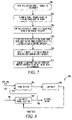
- FIG. 7 is a procedure for generating RF signals for transmission in accordance with some embodiments of the present invention.
- Procedure 700 may be performed by multicarrier transmitter 100 , although other transmitters may also be suitable.
- Operation 702 comprises decomposing digital baseband signals to generate phase-selection signals.
- operation 702 may be performed by coordinate rotation circuitry 110 ( FIG. 1 ), digital adder elements 112 ( FIG. 1 ) and delta-sigma modulators 114 A & 114 B ( FIG. 1 ) to generate phase-selection signals 115 A & 115 B ( FIG. 1 ), although the scope of the invention is not limited in this respect.
- Operation 704 comprises generating a plurality of phases of a square-wave signal at a transmit frequency.
- operation 704 may be performed by tapped delay-lines 106 A & 106 B ( FIG. 1 ) to provide phases 107 ( FIG. 1 ), although the scope of the invention is not limited in this respect.
- Operation 706 comprises selecting one of the phases of the square-wave signals based on the phase-selection signals to provide outphased switching waveforms.
- operation 706 may be performed by phase multiplexers 116 A & 116 B ( FIG. 1 ), although the scope of the invention is not limited in this respect.
- digital delay-line 600 ( FIG. 6 ) may perform both operations 704 and 706 .
- Operation 708 comprises separately amplifying the outphased switching waveforms with switching power amplifiers.
- operation 708 may be performed by switching power amplifiers 118 A & 118 B ( FIG. 1 ), although the scope of the invention is not limited in this respect.
- Operation 710 comprises combining the separately amplified outphased switching waveforms to generate an RF signal for transmission.
- operation 710 may be performed by combiner 120 ( FIG. 1 ), although the scope of the invention is not limited in this respect.
- procedure 700 may refer to an action and/or process of one or more processing or computing systems or similar devices that may manipulate and transform data represented as physical (e.g., electronic) quantities within a processing system's registers and memory into other data similarly represented as physical quantities within the processing system's registers or memories, or other such information storage, transmission or display devices.
- a computing device includes one or more processing elements coupled with computer-readable memory that may be volatile or non-volatile memory or a combination thereof.
- FIG. 8 illustrates a phase filter suitable for use with some embodiments of the present invention.
- Phase filter 800 may be suitable for use as phase filter 128 A ( FIG. 1 ) and/or phase filter 128 B ( FIG. 1 ), although other types of phase filters may also be suitable.
- Phase filter 800 includes phase detector 802 , loop filter 804 and continuously variable delay-line 806 . Continuously variable delay-line 806 delays square-wave signal 805 based on the output of loop filter 804 , and phase detector 802 compares the phases of input signal 817 with output signal 819 to generate a phase-difference output for loop filter 804 .
- phase filter 800 when phase filter 800 is used for phase filter 128 A ( FIG. 1 ), input signal 817 may correspond to outphased switching waveform 117 A ( FIG. 1 ) provided by phase multiplexer 116 A ( FIG. 1 ), and output signal 819 may correspond to the outphased switching waveform provided to power amplifier 118 A ( FIG. 1 ).
- the delay provided by continuously variable delay-line 806 may comprise a replica of the delay provided by tapped delay-line 106 A ( FIG. 1 ).
- phase filter 800 when phase filter 800 is used for phase filter 128 B ( FIG. 1 ), input signal 817 may correspond to outphased switching waveform 117 B ( FIG. 1 ) provided by phase multiplexer 116 B ( FIG. 1 ), and output signal 819 may correspond to the outphased switching waveform provided to power amplifier 118 B ( FIG. 1 ).
- the delay provided by continuously variable delay-line 806 may comprise a replica of the delay provided by tapped delay-line 106 B ( FIG. 1 ).
- square-wave signal 805 may correspond to square-wave signal 105 ( FIG. 1 ), and the operation of loop filter 804 and continuously variable delay-line 806 may remove out-of-band components from output signal 819 . This may result in more efficient amplification by the power amplifiers, although the scope of the invention is not limited in this respect.
- FIG. 9 is a functional block diagram of a polar transmitter in accordance with some embodiments of the present invention.
- Polar transmitter 900 comprises tapped delay-line 906 to provide a plurality of phases 907 of square-wave signal 905 at the transmit frequency, and phase multiplexer (MUX) 916 to select one of phases 907 based on phase-selection signal 915 to provide switching waveform 917 .
- phase-selection signal 915 may be generated by decomposing digital baseband signals 909 A & 909 B.
- Switching waveform 917 may be used to generate RF signal 921 for transmission.
- switching waveform 917 may comprise a substantially constant-envelope signal.
- coordinate rotation circuitry 910 may decompose I and Q components of digital baseband signals 909 A & 909 B into phi component 911 and amplitude component 913 .
- Switching waveform 917 may comprise square-wave signal 905 delayed by phi component 911 .
- polar transmitter 900 may also include power digital-to-analog converter (DAC) 918 to convert switching waveform 917 to RF signal 921 , and amplitude modulator 936 to amplitude-modulate the components of RF signal 921 based on amplitude component 913 provided by coordinate rotation circuitry 910 .
- the output of power DAC 918 may be amplified by one or more power amplifiers prior to transmission by one or more antennas. In some alternate embodiments, one or more switching power amplifiers may be used in place of power DAC 918 , although the scope of the invention is not limited in this respect.
- polar transmitter 900 may also comprise phase filter 928 to help remove out-of-band components from switching waveform 917 prior to amplification by power DAC 918 .
- Phase filter 800 ( FIG. 8 ) may be suitable for use as phase filter 928 , although other phase filters and DLLs may also be suitable.
- input bit stream 901 may correspond to input bit stream 101 ( FIG. 1 )
- digital baseband processor 908 may be similar to digital baseband processor 108 ( FIG. 1 )
- components of digital baseband signals 909 A & 909 B may correspond respectively to components of digital baseband signals 109 A & 109 B.
- coordinate rotation circuitry 910 may be similar to coordinate rotation circuitry 110 ( FIG. 1 )
- delta-sigma ( ⁇ - ⁇ ) modulator 914 may be similar to either delta-sigma ( ⁇ - ⁇ ) modulator 114 A or 114 B ( FIG. 1 )
- tapped delay-line 906 may be similar to either tapped delay-line 106 A or 106 B ( FIG.
- phase multiplexer 916 may be similar to either phase multiplexer 116 A or 116 B ( FIG. 1 ).
- signal generator 902 may be similar to signal generator 102 ( FIG. 1 ) and buffer 904 may be similar to buffer 104 ( FIG. 1 ).
- Some embodiments of the invention may be implemented a combination of hardware, firmware and/or software. Some embodiments of the invention may also be implemented as instructions stored on a machine-readable medium, which may be read and executed by at least one processor to perform the operations described herein.
- a machine-readable medium may include any mechanism for storing or transmitting information in a form readable by a machine (e.g., a computer).
- a machine-readable medium may include read-only memory (ROM), random-access memory (RAM), magnetic disk storage media, optical storage media, flash-memory devices, electrical, optical, acoustical or other form of propagated signals (e.g., carrier waves, infrared signals, digital signals, etc.), and others.
Landscapes
- Engineering & Computer Science (AREA)
- Power Engineering (AREA)
- Computer Networks & Wireless Communication (AREA)
- Signal Processing (AREA)
- Amplifiers (AREA)
- Transmitters (AREA)
Abstract
Description
Claims (28)
Priority Applications (1)
| Application Number | Priority Date | Filing Date | Title |
|---|---|---|---|
| US11/464,352 US7715493B2 (en) | 2006-08-14 | 2006-08-14 | Digital transmitter and methods of generating radio-frequency signals using time-domain outphasing |
Applications Claiming Priority (1)
| Application Number | Priority Date | Filing Date | Title |
|---|---|---|---|
| US11/464,352 US7715493B2 (en) | 2006-08-14 | 2006-08-14 | Digital transmitter and methods of generating radio-frequency signals using time-domain outphasing |
Publications (2)
| Publication Number | Publication Date |
|---|---|
| US20080037662A1 US20080037662A1 (en) | 2008-02-14 |
| US7715493B2 true US7715493B2 (en) | 2010-05-11 |
Family
ID=39050749
Family Applications (1)
| Application Number | Title | Priority Date | Filing Date |
|---|---|---|---|
| US11/464,352 Active 2029-01-20 US7715493B2 (en) | 2006-08-14 | 2006-08-14 | Digital transmitter and methods of generating radio-frequency signals using time-domain outphasing |
Country Status (1)
| Country | Link |
|---|---|
| US (1) | US7715493B2 (en) |
Cited By (10)
| Publication number | Priority date | Publication date | Assignee | Title |
|---|---|---|---|---|
| US20080200199A1 (en) * | 2003-05-09 | 2008-08-21 | Philips Intellectual Property & Standards Gmbh | Method and Arrangement For Setting the Transmission of a Mobile Communication Device |
| US20100240331A1 (en) * | 2007-09-27 | 2010-09-23 | Kyocera Corporation | Power amplifying circuit, and transmitter and wireless communication device using the same |
| US20120071196A1 (en) * | 2010-01-15 | 2012-03-22 | Telefonaktiebolaget Lm Ericsson (Publ) | Method And Apparatuses For Transmitter To Multi-Carrier Power Amplifier Configuration |
| US20120288018A1 (en) * | 2011-05-09 | 2012-11-15 | Saleh Osman | Efficient cartesian transmitter using signal combiner |
| US8736338B2 (en) * | 2012-04-11 | 2014-05-27 | Freescale Semiconductor, Inc. | High precision single edge capture and delay measurement circuit |
| US20140266820A1 (en) * | 2013-03-15 | 2014-09-18 | Lsi Corporation | Interleaved multipath digital power amplification |
| US8890634B2 (en) * | 2012-10-26 | 2014-11-18 | Mstar Semiconductor, Inc. | Multiplexed configurable sigma delta modulators for noise shaping in a 25-percent duty cycle digital transmitter |
| US9473340B2 (en) * | 2014-12-15 | 2016-10-18 | Apple Inc. | Orthogonal frequency division multiplexing polar transmitter |
| US10258803B2 (en) | 2014-06-30 | 2019-04-16 | Advanced Bionics Ag | Radio frequency transmitter circuits that provide power to an implant device |
| US10720928B1 (en) * | 2019-03-12 | 2020-07-21 | United States Of America As Represented By The Secretary Of The Air Force | Frequency agile modulator |
Families Citing this family (19)
| Publication number | Priority date | Publication date | Assignee | Title |
|---|---|---|---|---|
| US20080238621A1 (en) * | 2007-03-30 | 2008-10-02 | Broadcom Corporation | Multi-mode rfid reader architecture |
| US7889811B2 (en) * | 2007-09-06 | 2011-02-15 | Samsung Electro-Mechanics | Digital linear amplification with nonlinear components (LINC) transmitter |
| US8044742B2 (en) | 2009-03-11 | 2011-10-25 | Qualcomm Incorporated | Wideband phase modulator |
| US20100283665A1 (en) * | 2009-05-05 | 2010-11-11 | Imran Bashir | Mitigation of RF Oscillator Pulling through Adjustable Phase Shifting |
| US8588720B2 (en) * | 2009-12-15 | 2013-11-19 | Qualcomm Incorproated | Signal decimation techniques |
| US8909065B2 (en) * | 2011-07-15 | 2014-12-09 | Intel Mobile Communications GmbH | Adjustable delayer, method for delaying an input signal and polar transmitter |
| US20140218009A1 (en) * | 2011-08-29 | 2014-08-07 | Asahi Kasei Microdevices Corporation | Device for measuring a duration of a level of an electrical signal |
| US8831158B2 (en) | 2012-03-29 | 2014-09-09 | Broadcom Corporation | Synchronous mode tracking of multipath signals |
| US9000858B2 (en) | 2012-04-25 | 2015-04-07 | Qualcomm Incorporated | Ultra-wide band frequency modulator |
| US9172329B2 (en) * | 2012-08-01 | 2015-10-27 | Nxp B.V. | Harmonic suppression in switching amplifiers |
| US9178541B2 (en) * | 2013-10-24 | 2015-11-03 | Marvell World Trade Ltd. | Cartesian digital power amplifier using coordinate rotation |
| CN110291723B (en) * | 2016-11-25 | 2021-04-09 | 华为技术有限公司 | Polarized phased array transmitter and mobile terminal |
| KR20200086628A (en) * | 2017-12-28 | 2020-07-17 | 아셀산 엘렉트로닉 사나이 베 티카렛 아노님 시르케티 | All digital outpage transmitters |
| EP3629483B1 (en) * | 2018-09-28 | 2020-12-09 | Nxp B.V. | Transmitter circuit for rf communication device, rf communication device, and method of generating an antenna output signal in a transmitter circuit |
| TWI716975B (en) * | 2019-08-21 | 2021-01-21 | 智原科技股份有限公司 | Time detection circuit and time detection method thereof |
| US11469721B2 (en) | 2020-01-08 | 2022-10-11 | Qorvo Us, Inc. | Uplink multiple input-multiple output (MIMO) transmitter apparatus |
| US11336240B2 (en) * | 2020-01-16 | 2022-05-17 | Qorvo Us, Inc. | Uplink multiple input-multiple output (MIMO) transmitter apparatus using transmit diversity |
| US11387795B2 (en) | 2020-01-28 | 2022-07-12 | Qorvo Us, Inc. | Uplink multiple input-multiple output (MIMO) transmitter apparatus with pre-distortion |
| WO2023247597A1 (en) * | 2022-06-21 | 2023-12-28 | Imec Vzw | Amplifier |
Citations (5)
| Publication number | Priority date | Publication date | Assignee | Title |
|---|---|---|---|---|
| US6337606B1 (en) * | 1999-02-02 | 2002-01-08 | Sicom, Inc. | Digital communications modulator having a modulation processor which supports high data rates |
| US6377967B1 (en) * | 1998-08-12 | 2002-04-23 | Northrop Grumman Corporation | Efficient digital integration technique filter |
| US6490440B1 (en) * | 1999-06-01 | 2002-12-03 | Motorola, Inc. | Digital transmitter circuit and method of operation |
| US6996191B1 (en) * | 1999-09-30 | 2006-02-07 | Skyworks Solutions, Inc. | Efficient accurate controller for envelope feedforward power amplifiers |
| US7012477B2 (en) * | 2003-11-28 | 2006-03-14 | Vcom Inc. | Modulation using discrete amplitude adjustment and dual digital delay lines |
-
2006
- 2006-08-14 US US11/464,352 patent/US7715493B2/en active Active
Patent Citations (6)
| Publication number | Priority date | Publication date | Assignee | Title |
|---|---|---|---|---|
| US6377967B1 (en) * | 1998-08-12 | 2002-04-23 | Northrop Grumman Corporation | Efficient digital integration technique filter |
| US6337606B1 (en) * | 1999-02-02 | 2002-01-08 | Sicom, Inc. | Digital communications modulator having a modulation processor which supports high data rates |
| US6362701B1 (en) * | 1999-02-02 | 2002-03-26 | Sicom, Inc. | Digital communications modulator having an interpolator upstream of a linearizer and method therefor |
| US6490440B1 (en) * | 1999-06-01 | 2002-12-03 | Motorola, Inc. | Digital transmitter circuit and method of operation |
| US6996191B1 (en) * | 1999-09-30 | 2006-02-07 | Skyworks Solutions, Inc. | Efficient accurate controller for envelope feedforward power amplifiers |
| US7012477B2 (en) * | 2003-11-28 | 2006-03-14 | Vcom Inc. | Modulation using discrete amplitude adjustment and dual digital delay lines |
Non-Patent Citations (4)
| Title |
|---|
| Bateman, A., "The Combined Analogue Locked Loop Universal Modulator (CALLUM)", Proceedings, 42nd VTS Conference-Frontiers of Technology, vol. 2, (May 10-13, 1992, Denver, CO, (1992), 759-763. |
| Chireix, H., "High Power Outphasing Modulation", Proceedings of the Institute of Radio Engineers (IRE) vol. 23, No. 11, (Nov. 1935), 1370-1392. |
| Cox, D. C., "Linear Amplification With Nonlinear Components", IEEE Transactions on Communications, vol. COM-22, No. 12, (Dec. 1974), 1942-1945. |
| Hamedi-Hagh, S., et al., "CMOS Wireless Phase-Shifted Transmitter", IEEE Journal of Solid-State Circuits, vol. 39 No. 8, (Aug. 2004), 1241-1252. |
Cited By (15)
| Publication number | Priority date | Publication date | Assignee | Title |
|---|---|---|---|---|
| US20080200199A1 (en) * | 2003-05-09 | 2008-08-21 | Philips Intellectual Property & Standards Gmbh | Method and Arrangement For Setting the Transmission of a Mobile Communication Device |
| US7809393B2 (en) * | 2003-05-09 | 2010-10-05 | Nxp B.V. | Method and arrangement for setting the transmission of a mobile communication device |
| US20100240331A1 (en) * | 2007-09-27 | 2010-09-23 | Kyocera Corporation | Power amplifying circuit, and transmitter and wireless communication device using the same |
| US8463202B2 (en) * | 2007-09-27 | 2013-06-11 | Kyocera Corporation | Power amplifying circuit, and transmitter and wireless communication device using the same |
| US20120071196A1 (en) * | 2010-01-15 | 2012-03-22 | Telefonaktiebolaget Lm Ericsson (Publ) | Method And Apparatuses For Transmitter To Multi-Carrier Power Amplifier Configuration |
| US8718583B2 (en) * | 2010-01-15 | 2014-05-06 | Telefonaktiebolaget L M Ericsson (Publ) | Method and apparatuses for transmitter to multi-carrier power amplifier configuration |
| US8477857B2 (en) * | 2011-05-09 | 2013-07-02 | Panasonic Corporation | Efficient cartesian transmitter using signal combiner |
| US20120288018A1 (en) * | 2011-05-09 | 2012-11-15 | Saleh Osman | Efficient cartesian transmitter using signal combiner |
| US8736338B2 (en) * | 2012-04-11 | 2014-05-27 | Freescale Semiconductor, Inc. | High precision single edge capture and delay measurement circuit |
| US8890634B2 (en) * | 2012-10-26 | 2014-11-18 | Mstar Semiconductor, Inc. | Multiplexed configurable sigma delta modulators for noise shaping in a 25-percent duty cycle digital transmitter |
| US20140266820A1 (en) * | 2013-03-15 | 2014-09-18 | Lsi Corporation | Interleaved multipath digital power amplification |
| US8970406B2 (en) * | 2013-03-15 | 2015-03-03 | Lsi Corporation | Interleaved multipath digital power amplification |
| US10258803B2 (en) | 2014-06-30 | 2019-04-16 | Advanced Bionics Ag | Radio frequency transmitter circuits that provide power to an implant device |
| US9473340B2 (en) * | 2014-12-15 | 2016-10-18 | Apple Inc. | Orthogonal frequency division multiplexing polar transmitter |
| US10720928B1 (en) * | 2019-03-12 | 2020-07-21 | United States Of America As Represented By The Secretary Of The Air Force | Frequency agile modulator |
Also Published As
| Publication number | Publication date |
|---|---|
| US20080037662A1 (en) | 2008-02-14 |
Similar Documents
| Publication | Publication Date | Title |
|---|---|---|
| US7715493B2 (en) | Digital transmitter and methods of generating radio-frequency signals using time-domain outphasing | |
| US7729445B2 (en) | Digital outphasing transmitter architecture | |
| US7061989B2 (en) | Fully digital transmitter including a digital band-pass sigma-delta modulator | |
| JP5781872B2 (en) | Wireless transmitter | |
| EP3219063B1 (en) | System and method for generating a multi-band signal | |
| US10541657B2 (en) | Method and apparatus for digital pre-distortion with reduced oversampling output ratio | |
| US8112047B2 (en) | Configurable RF transmitter | |
| US9647866B2 (en) | RF transmitter, integrated circuit device, wireless communication unit and method therefor | |
| EP2515444B1 (en) | RF transmitter and method therefor | |
| US20090034603A1 (en) | Subranging for a pulse position and pulse width modulation based transmitter | |
| WO2009018401A1 (en) | Digital integrated transmitter based on four-path phase modulation | |
| US9166617B1 (en) | Communication unit, digital band-pass sigma-delta modulator and method therefor | |
| EP3807999B1 (en) | Mixed-mode millimeter-wave transmitter | |
| US11483186B2 (en) | Ultra-high data rate digital mm-wave transmitter with energy efficient spectral filtering | |
| US10523478B1 (en) | System and method for generating high speed digitized-RF signals | |
| JP2009171460A (en) | Communication device, oscillator and frequency synthesizer | |
| US8077803B2 (en) | Quarter duty cycle pulse generator for interleaved switching mixer | |
| Chung et al. | A concurrent triple-band digital transmitter using feedforward noise cancellation for delta-sigma modulation | |
| Chung et al. | Outphasing multi-level RF-PWM signals for inter-band carrier aggregation in digital transmitters | |
| WO2015114702A1 (en) | Transmission device and method for controlling same | |
| WO2018063661A1 (en) | Device and method to reduce power amplifier power consumption | |
| US20180262383A1 (en) | An apparatus and a method for generating a radio frequency signal | |
| Vasilakopoulos | Mixed-Signal Processing Techniques for RF Transmitters | |
| Berland et al. | Digital signal processing techniques to compensate for RF imperfections in advanced transmitter architectures | |
| Nuyts et al. | Digital Transmitter Architectures: Overview |
Legal Events
| Date | Code | Title | Description |
|---|---|---|---|
| AS | Assignment |
Owner name: INTEL CORPORATION, CALIFORNIA Free format text: ASSIGNMENT OF ASSIGNORS INTEREST;ASSIGNORS:RAVI, ASHOKE;NAIKNAWARE, RAVI;SOUMYANATH, KRISHNAMURTHY;REEL/FRAME:020604/0312;SIGNING DATES FROM 20060808 TO 20060809 Owner name: INTEL CORPORATION,CALIFORNIA Free format text: ASSIGNMENT OF ASSIGNORS INTEREST;ASSIGNORS:RAVI, ASHOKE;NAIKNAWARE, RAVI;SOUMYANATH, KRISHNAMURTHY;SIGNING DATES FROM 20060808 TO 20060809;REEL/FRAME:020604/0312 |
|
| FEPP | Fee payment procedure |
Free format text: PAYOR NUMBER ASSIGNED (ORIGINAL EVENT CODE: ASPN); ENTITY STATUS OF PATENT OWNER: LARGE ENTITY |
|
| STCF | Information on status: patent grant |
Free format text: PATENTED CASE |
|
| CC | Certificate of correction | ||
| REMI | Maintenance fee reminder mailed | ||
| FPAY | Fee payment |
Year of fee payment: 4 |
|
| SULP | Surcharge for late payment | ||
| MAFP | Maintenance fee payment |
Free format text: PAYMENT OF MAINTENANCE FEE, 8TH YEAR, LARGE ENTITY (ORIGINAL EVENT CODE: M1552) Year of fee payment: 8 |
|
| AS | Assignment |
Owner name: GUANGDONG OPPO MOBILE TELECOMMUNICATIONS CORP., LT Free format text: ASSIGNMENT OF ASSIGNORS INTEREST;ASSIGNOR:SKY ROYAL TRADING LIMITED;REEL/FRAME:044750/0068 Effective date: 20180117 Owner name: SKY ROYAL TRADING LIMITED, HONG KONG Free format text: ASSIGNMENT OF ASSIGNORS INTEREST;ASSIGNOR:INTEL CORPORATION;REEL/FRAME:045171/0323 Effective date: 20170911 |
|
| MAFP | Maintenance fee payment |
Free format text: PAYMENT OF MAINTENANCE FEE, 12TH YEAR, LARGE ENTITY (ORIGINAL EVENT CODE: M1553); ENTITY STATUS OF PATENT OWNER: LARGE ENTITY Year of fee payment: 12 |