US7486017B2 - Display device - Google Patents
Display device Download PDFInfo
- Publication number
- US7486017B2 US7486017B2 US11/073,522 US7352205A US7486017B2 US 7486017 B2 US7486017 B2 US 7486017B2 US 7352205 A US7352205 A US 7352205A US 7486017 B2 US7486017 B2 US 7486017B2
- Authority
- US
- United States
- Prior art keywords
- substrate
- gas barrier
- barrier layer
- display device
- neutral plane
- Prior art date
- Legal status (The legal status is an assumption and is not a legal conclusion. Google has not performed a legal analysis and makes no representation as to the accuracy of the status listed.)
- Active, expires
Links
- 239000000758 substrate Substances 0.000 claims abstract description 145
- 230000004888 barrier function Effects 0.000 claims abstract description 117
- 230000007935 neutral effect Effects 0.000 claims abstract description 55
- 238000005452 bending Methods 0.000 claims abstract description 8
- 239000000463 material Substances 0.000 claims description 15
- 239000011347 resin Substances 0.000 claims description 9
- 229920005989 resin Polymers 0.000 claims description 9
- 229910052814 silicon oxide Inorganic materials 0.000 claims description 7
- VYPSYNLAJGMNEJ-UHFFFAOYSA-N Silicium dioxide Chemical compound O=[Si]=O VYPSYNLAJGMNEJ-UHFFFAOYSA-N 0.000 claims description 5
- TWNQGVIAIRXVLR-UHFFFAOYSA-N oxo(oxoalumanyloxy)alumane Chemical compound O=[Al]O[Al]=O TWNQGVIAIRXVLR-UHFFFAOYSA-N 0.000 claims description 4
- -1 silicon oxide nitride Chemical class 0.000 claims description 3
- 229910052581 Si3N4 Inorganic materials 0.000 claims description 2
- 229910004205 SiNX Inorganic materials 0.000 claims description 2
- 229910020286 SiOxNy Inorganic materials 0.000 claims description 2
- HQVNEWCFYHHQES-UHFFFAOYSA-N silicon nitride Chemical compound N12[Si]34N5[Si]62N3[Si]51N64 HQVNEWCFYHHQES-UHFFFAOYSA-N 0.000 claims description 2
- 239000010410 layer Substances 0.000 description 132
- 239000007789 gas Substances 0.000 description 104
- 239000010408 film Substances 0.000 description 26
- 238000000034 method Methods 0.000 description 16
- 229910052751 metal Inorganic materials 0.000 description 10
- 239000002184 metal Substances 0.000 description 10
- QVGXLLKOCUKJST-UHFFFAOYSA-N atomic oxygen Chemical compound [O] QVGXLLKOCUKJST-UHFFFAOYSA-N 0.000 description 8
- 239000011248 coating agent Substances 0.000 description 8
- 239000011247 coating layer Substances 0.000 description 8
- 238000000576 coating method Methods 0.000 description 8
- 230000006835 compression Effects 0.000 description 8
- 238000007906 compression Methods 0.000 description 8
- 239000001301 oxygen Substances 0.000 description 8
- 229910052760 oxygen Inorganic materials 0.000 description 8
- XLYOFNOQVPJJNP-UHFFFAOYSA-N water Substances O XLYOFNOQVPJJNP-UHFFFAOYSA-N 0.000 description 7
- 238000000151 deposition Methods 0.000 description 6
- 230000008021 deposition Effects 0.000 description 6
- 230000000694 effects Effects 0.000 description 6
- 150000002894 organic compounds Chemical class 0.000 description 5
- 230000006866 deterioration Effects 0.000 description 4
- 230000000149 penetrating effect Effects 0.000 description 4
- 238000002347 injection Methods 0.000 description 3
- 239000007924 injection Substances 0.000 description 3
- 239000007788 liquid Substances 0.000 description 3
- 238000002161 passivation Methods 0.000 description 3
- 229920000642 polymer Polymers 0.000 description 3
- 238000007789 sealing Methods 0.000 description 3
- 239000000243 solution Substances 0.000 description 3
- XOLBLPGZBRYERU-UHFFFAOYSA-N tin dioxide Chemical compound O=[Sn]=O XOLBLPGZBRYERU-UHFFFAOYSA-N 0.000 description 3
- 238000013459 approach Methods 0.000 description 2
- 238000007664 blowing Methods 0.000 description 2
- 230000002542 deteriorative effect Effects 0.000 description 2
- 229910052737 gold Inorganic materials 0.000 description 2
- 239000010931 gold Substances 0.000 description 2
- BASFCYQUMIYNBI-UHFFFAOYSA-N platinum Chemical compound [Pt] BASFCYQUMIYNBI-UHFFFAOYSA-N 0.000 description 2
- 230000001681 protective effect Effects 0.000 description 2
- 238000001771 vacuum deposition Methods 0.000 description 2
- 239000012790 adhesive layer Substances 0.000 description 1
- 229910052784 alkaline earth metal Inorganic materials 0.000 description 1
- 150000001342 alkaline earth metals Chemical class 0.000 description 1
- 239000000956 alloy Substances 0.000 description 1
- 229910045601 alloy Inorganic materials 0.000 description 1
- 229910052782 aluminium Inorganic materials 0.000 description 1
- 229910052791 calcium Inorganic materials 0.000 description 1
- 150000001875 compounds Chemical class 0.000 description 1
- 230000007547 defect Effects 0.000 description 1
- 238000001035 drying Methods 0.000 description 1
- 238000005401 electroluminescence Methods 0.000 description 1
- PCHJSUWPFVWCPO-UHFFFAOYSA-N gold Chemical compound [Au] PCHJSUWPFVWCPO-UHFFFAOYSA-N 0.000 description 1
- AMGQUBHHOARCQH-UHFFFAOYSA-N indium;oxotin Chemical compound [In].[Sn]=O AMGQUBHHOARCQH-UHFFFAOYSA-N 0.000 description 1
- 238000007733 ion plating Methods 0.000 description 1
- 238000003475 lamination Methods 0.000 description 1
- 239000004973 liquid crystal related substance Substances 0.000 description 1
- 229920002521 macromolecule Polymers 0.000 description 1
- 229910052749 magnesium Inorganic materials 0.000 description 1
- 239000011159 matrix material Substances 0.000 description 1
- 239000007769 metal material Substances 0.000 description 1
- 239000000203 mixture Substances 0.000 description 1
- 230000035515 penetration Effects 0.000 description 1
- 229910052697 platinum Inorganic materials 0.000 description 1
- 229920000767 polyaniline Polymers 0.000 description 1
- 229920000128 polypyrrole Polymers 0.000 description 1
- 229920000123 polythiophene Polymers 0.000 description 1
- 230000001737 promoting effect Effects 0.000 description 1
- 230000027756 respiratory electron transport chain Effects 0.000 description 1
- 229910052709 silver Inorganic materials 0.000 description 1
- 238000004544 sputter deposition Methods 0.000 description 1
- 239000010409 thin film Substances 0.000 description 1
- 229910001887 tin oxide Inorganic materials 0.000 description 1
- 238000004804 winding Methods 0.000 description 1
- YVTHLONGBIQYBO-UHFFFAOYSA-N zinc indium(3+) oxygen(2-) Chemical compound [O--].[Zn++].[In+3] YVTHLONGBIQYBO-UHFFFAOYSA-N 0.000 description 1
Images


Classifications
-
- H—ELECTRICITY
- H10—SEMICONDUCTOR DEVICES; ELECTRIC SOLID-STATE DEVICES NOT OTHERWISE PROVIDED FOR
- H10K—ORGANIC ELECTRIC SOLID-STATE DEVICES
- H10K59/00—Integrated devices, or assemblies of multiple devices, comprising at least one organic light-emitting element covered by group H10K50/00
- H10K59/80—Constructional details
- H10K59/87—Passivation; Containers; Encapsulations
- H10K59/873—Encapsulations
-
- H—ELECTRICITY
- H10—SEMICONDUCTOR DEVICES; ELECTRIC SOLID-STATE DEVICES NOT OTHERWISE PROVIDED FOR
- H10K—ORGANIC ELECTRIC SOLID-STATE DEVICES
- H10K50/00—Organic light-emitting devices
- H10K50/80—Constructional details
- H10K50/84—Passivation; Containers; Encapsulations
- H10K50/844—Encapsulations
-
- H—ELECTRICITY
- H10—SEMICONDUCTOR DEVICES; ELECTRIC SOLID-STATE DEVICES NOT OTHERWISE PROVIDED FOR
- H10K—ORGANIC ELECTRIC SOLID-STATE DEVICES
- H10K2102/00—Constructional details relating to the organic devices covered by this subclass
- H10K2102/301—Details of OLEDs
- H10K2102/311—Flexible OLED
-
- H—ELECTRICITY
- H10—SEMICONDUCTOR DEVICES; ELECTRIC SOLID-STATE DEVICES NOT OTHERWISE PROVIDED FOR
- H10K—ORGANIC ELECTRIC SOLID-STATE DEVICES
- H10K59/00—Integrated devices, or assemblies of multiple devices, comprising at least one organic light-emitting element covered by group H10K50/00
- H10K59/10—OLED displays
- H10K59/17—Passive-matrix OLED displays
Definitions
- This invention relates to a display device, and more particularly to a display device such as an organic EL (electroluminescence) element where a display portion is formed on a substrate.
- a display device such as an organic EL (electroluminescence) element where a display portion is formed on a substrate.
- an organic EL element comprising an insulating transparent substrate, a plurality of transparent anodes on the substrate spaced from each other, an organic compound layer which includes at least a light emitting layer and is formed to cover the transparent anodes, and metal cathodes opposed to the transparent anodes intervening therebetween the organic compound layer.
- the light emitting layer included in the organic compound layer emits light when an electric current flows between the transparent anodes and the metal cathodes, and the light is taken out through the transparent anodes and the transparent substrate. That is, in the organic EL element, each intersection of the transparent anodes and the metal cathodes forms a light emitting portion and light emitting portions can be controlled to emit light (light-emission) and not to emit light (non-light-emission) independently of each other.
- the organic EL element is excellent in wavelength stability.
- the display device where a display portion is formed on a substrate like an organic EL element, especially, when a resin substrate formed of macromolecular material is used as the substrate, there has been a problem that oxygen or water passing through the substrate can penetrate to the display portion to deteriorate the display portion.
- a gas barrier layer between at least a part of the substrate and a display portion as disclosed, for instance, in Japanese Patent No. 2911552 and/or Japanese Unexamined Patent Publication No. 2002-18994.
- the gas barrier layer is a layer which basically blocks gases but naturally blocks liquids.
- the primary object of the present invention is to provide a display device where even if the device undergoes external force to bend the substrate, the gas barrier layer is not easily damaged.
- a display device comprising a substrate, a display portion formed on the substrate, an upper layer which covers the display portion, and a gas barrier layer provided between at least a part of the substrate and the display portion, wherein the improvement comprises that the gas barrier layer is positioned near to the position which forms a neutral plane (a plane in which neither tensile stress nor compression stress is generated) when bending moment in a direction in which the substrate is warped acts on the overall display device.
- the upper layer be formed by the same material as the substrate.
- the distance between the neutral plane and the gas barrier layer be not larger than 30% of the distance between the neutral plane and the surface of the substrate on the side of the gas barrier layer.
- the display portion be positioned near to the position which forms a neutral plane.
- the distance between the neutral plane and the display portion be not larger than 30% of the distance between the neutral plane and the surface of the substrate on the side of the display portion.
- the display device of the present invention further comprises a second gas barrier layer formed on the side of the display portion opposite to the substrate, it is preferred that the second gas barrier layer is also positioned near to the position which forms a neutral plane.
- the present invention be applied to a display device where a resin substrate formed of macromolecular material is used as the substrate.
- the present invention be applied to a display device comprising an organic EL element.
- a gas barrier layer is provided between at least a part of the substrate and the display portion near to the position which forms a neutral plane, no or very small tensile stress or compression stress is generated in the gas barrier layer when the device undergoes external force which warps the substrate, whereby the gas barrier layer is prevented from being damaged.
- the gas barrier layers 3 and 4 are provided on the surfaces of the substrate 2 as shown in FIG. 2 , tensile stress and compression stress are generated respectively on the outer and inner sides of the substrate 2 each time the substrate 2 is bent. Due to these stresses, the dense gas barrier layers 3 and 4 deteriorate, and a defect such as cracks is locally generated to deteriorate the barrier performance of the gas barrier layers 3 and 4 to permit penetration of oxygen and water from the external, thereby promoting deterioration of the organic EL element.
- the neutral plane a plane where the stress is nullified
- no stress is generated in response to bending of the substrate.
- the modulus of longitudinal elasticity of the substrate 10 is uniform over the entire area thereof, the thicknesses of the substrate 10 above and below the gas barrier layer 20 are substantially equal to each other.
- the display portion 30 may be disposed, for instance, near to the neutral plane N as shown in FIG. 3 . In the example shown FIG.
- the display portion 30 is formed on the lower substrate 10 and the upper substrate 10 is formed of the same material as the lower substrate 10 over the lower substrate 10 as the upper layer which covers the display portion 30 .
- the upper layer may be formed of material different from that of the lower substrate 10 .
- the modulus of longitudinal elasticity of each of the substrates 10 above and below the gas barrier layer 20 is a function E(y) of the position y in the direction of thickness
- the thicknesses y 1 and y 2 of the respective substrates 10 are determined to satisfy formula
- the gas barrier layer is sandwiched between a pair of substrates.
- one of the substrates is protective film, for instance, of polymer formed by application. That is, in this case, the protective film forms the upper layer described above.
- the gas barrier layer may be of a multiple layers.
- the display portion is abbreviated in FIGS. 4 and 5 and FIG. 6 to be described later.
- EB and ES respectively represent the moduli of longitudinal elasticity of the gas barrier layer 20 and the flexible substrate 10
- y 1 , y 2 and y 3 respectively represent the position of the surface of the substrate 10 opposite to the gas barrier layer 20 with the neutral plane N taken as the reference, the position of the surface of the substrate 10 on the side of the gas barrier layer 20 with the neutral plane N taken as the reference, and the position of the gas barrier layer 20 .
- the overall thickness t of the flexible substrate 10 is 0.2 mm where the flexibility and the strength are compatible with each other.
- y 3 20 ⁇ m from formula (3).
- FIG. 7 The result obtained by calculating ⁇ r characteristics by substituting the value in formula (4) is shown in FIG. 7 .
- the stress ⁇ in the gas barrier layer 20 increases. Since the tensile strength of Al 2 O 3 which is generally used as the gas barrier layer 20 is about 400 MPa, the gas barrier layer 20 is broken when the radius r of curvature of warpage of the substrate is reduced to not larger than 15 mm.
- the limit radius of curvature r becomes smaller and the display device can be wound to smaller radius.
- the limit radius of curvature r is not larger than half of that when the gas barrier layer is on the surface of the substrate and the winding dimension may be suppressed to half of that when the gas barrier layer is on the surface of the substrate.
- the gas barrier layer is near to the neutral plane N so that ⁇ is not larger than 0.3, that is, the distance between the neutral plane N and the gas barrier layer is not larger than 30% of the distance between the neutral plane and the surface of the substrate on the side of the gas barrier layer.
- the position of the neutral plane N is calculated by substituting the distribution of E(y) in formula (1) and the relation between the value of ⁇ and the limit radius of curvature r can be obtained by carrying out a calculation similar to that described above on the basis of the calculated position of the neutral plane N.
- the display device such as an organic EL element
- deterioration is promoted also in the display portion by bending stress of the substrate, and the service life of the display device is shortened.
- ITO or SnO 2 which is used as transparent electrodes in the display portion is relatively apt to be damaged by bending since they are oxide.
- FIG. 9 shows in brief this arrangement.
- the neutral plane is abbreviated in order to avoid the complication, it exists near to the gas barrier layer 20 and the display portion 30 which are sandwiched between the upper and lower substrates 10 .
- the position of the display portion be near to the neutral plane so that the distance between the neutral plane and the display portion is not larger than 30% of the distance between the neutral plane and the surface of the substrate on the side of the display portion for the same reason as discussed above on the position of the gas barrier layer by the use of the value of ⁇ .
- the resin substrate formed of macromolecule material is especially permeable to oxygen, it is especially useful to apply the present invention to a display device where a resin substrate is employed.
- the present invention is remarkably useful to prevent deterioration of the organic EL element.
- FIG. 1 is a view for illustrating the effect of the present invention
- FIG. 2 is a view for illustrating the effect of the present invention
- FIG. 3 is a view showing in brief a basic arrangement of the display device of the present invention.
- FIG. 4 is a view for illustrating the effect of the present invention
- FIG. 5 is a view for illustrating the effect of the present invention
- FIG. 6 is a view for illustrating the effect of the present invention.
- FIG. 7 is a graph showing the relation between the radius of curvature of the substrate and the stress acting on the gas barrier layer in the display device
- FIG. 8 is a graph showing the relation between the position of the gas barrier layer and the limit radius of curvature of the substrate in the display device
- FIG. 9 is a view showing in brief another arrangement of the display device of the present invention.
- FIG. 10 is a view showing in brief still another arrangement of the display device of the present invention.
- FIGS. 11A and 11B are respectively a plan view and a side view showing in brief an organic EL element in accordance with an embodiment of the present invention
- FIG. 12 is a view for illustrating a method of producing a display device in accordance with the present invention.
- FIG. 13 is a view for illustrating a method of producing a display device in accordance with the present invention.
- FIGS. 14A and 14B are views for illustrating a method of producing a display device in accordance with the present invention.
- FIGS. 15A to 15C are views for illustrating a method of producing a display device in accordance with the present invention.
- FIG. 16 is a view for illustrating a method of producing a display device in accordance with the present invention.
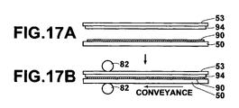
- FIGS. 17A and 17B are views for illustrating a method of producing a display device in accordance with the present invention.
- the organic EL element of this embodiment is flexible.
- the lower and upper substrates 50 and 53 are formed of flexible and transparent resin of, for instance, macromolecular material.
- the display portion 60 as in the usual organic EL element, comprises a plurality of transparent anode strips 61 spaced from each other, an insulating film 62 which is formed of, for instance, SiO 2 which covers the transparent anode strips 61 from above with predetermined parts of the transparent anode strips 61 exposed through openings 62 a , an organic EL layer 63 disposed on the transparent anode strips 61 , and a plurality of cathode strips 64 opposed to the exposed parts of the transparent anode strips 61 with the organic EL layer 63 intervening therebetween.
- the organic EL layer 63 as that of the usual organic EL element, comprises a positive hole transfer layer and a light emitting layer which are of organic compound. If desired, at least one suitable layer such as a positive hole injection layer, an electron injection layer, an electron transfer layer or the like may be added to the organic EL layer 63 .
- the cathode strips 64 are arranged in a direction perpendicular to the transparent anode strips 61 spaced from each other. With this arrangement, intersections of the transparent anode strips 61 and the cathode strips 64 (here, the transparent anode strip 61 is exposed through the opening 62 a of the insulating film 62 ) are arranged like a two-dimensional matrix, and each of the intersections forms a light emitting portion where the organic EL layer 63 is between the transparent anode strip 61 and the cathode strip 64 .
- a light emitting layer of each of the light emitting portions emits light independently of the other light emitting portions and the light is taken out through the transparent anode strip 61 and the transparent lower substrate 50 .
- the transparent anode strips 61 exhibit at least not smaller than 50% (preferably, not smaller than 70%) of light-transmittivity to light in a visible light wavelength range of 400 nm to 700 nm.
- the material of the transparent anode strips 61 compounds known as the material of the transparent electrode such as tin oxide, indium-tin oxide (ITO) or indium-zinc oxide may be used.
- film of metal such as gold or platinum which is large in work function may be used as the material of the transparent anode strips 61 .
- an organic compound such as polyaniline, polythiophene, polypyrrole or their derivatives may be used as the material of the transparent anode strips 61 .
- “New Stage of Transparent Conductive Film” (supervised by Yutaka Sawada, GMC CO., 1999) has described in detail the transparent conductive film and those disclosed there may be applied to the present invention.
- the cathode strips 64 be formed by metal material such as alkaline metal (e.g., Li or K), alkaline earth metal (e.g., Mg or Ca), or alloy or mixture of these metal which is small in work function. So that the can stability and electron injection are compatible with each other on the cathode, the electrode formed by the material described above may be coated with Ag, Al, Au or the like which is large in work function and high in conductivity.
- the cathode strips 64 as well as the transparent anode strips 61 may be formed by a known method such as vacuum deposition, sputtering, ion plating or the like.
- the first gas barrier layer (sealing film) 51 is formed by, for instance, aluminum oxide (Al 2 O 3 ), silicon oxide (SiO 2 ) or silicon oxide nitride (SiO x N y ) and has a function of shielding gas and liquid.
- the second gas barrier layer (passivation film) 52 is formed by, for instance, silicon nitride (SiN x ) and also has a function of shielding gas and liquid.
- the first and second gas barrier layers 51 and 52 and the display portion 60 are disposed near to the position which forms a neutral plane when bending moment in a direction in which the substrates 50 and 53 are warped acts on the overall display device.
- no or very small tensile stress or compression stress is generated in the gas barrier layers 51 and 52 and the display portion 60 even when the element undergoes external force which warps the substrate, whereby the gas barrier layers 51 and 52 and the display portion 60 are effectively prevented from being damaged whereby the service life of the organic EL element is elongated.
- the lower substrate 50 is held in a vacuum deposition pot 70 by a substrate holding jig 71 , and layer material 73 evaporated from a deposition source 72 is deposited on the lower substrate 50 through a mask 74 .
- a first gas barrier layer 51 can be formed on the lower substrate 50
- the display portion 60 comprising the transparent anode strips 61 , the insulating film 62 , the organic EL layer 63 , the cathode strips 64 and the like can be formed on the first gas barrier layer 51
- the second gas barrier layer 52 can be formed on the display portion 60 .
- coating solution is blown on the lower substrate 50 through, for instance, a plurality of nozzles 75 and 76 , whereby coating layers C 1 and C 2 which form the first gas barrier layer 51 , the display portion 60 , the second gas barrier layer 52 , and the like are formed.
- the coating layers C 1 and C 2 can be formed in desired patterns.
- a plurality of nozzles 75 and 76 a plurality of coating layers can be formed at one time, for example, the coating layer C 2 is formed on the coating layer C 1 .
- FIGS. 14A and 14B are, respectively, a side view and a plan view showing a state of forming a coating layer C which forms the first gas barrier layer 51 , the display portion 60 , the second gas barrier layer 52 or the like.
- a droplet 78 is blown on the lower substrate 50 from the ink jet head 77 .
- the coating layer C can be formed in a desired pattern.
- a plurality of coating layers forming the first gas barrier layer 51 , the display portion 60 and the second gas barrier layer 52 can be formed in sequence.
- a lower substrate 50 on which the first gas barrier layer 51 , the display portion 60 and the second gas barrier layer 52 (See FIG. 11 .
- the laminated film 90 ”.) have been formed by one of the above described methods is prepared. While the lower substrate 50 is conveyed in one direction, coating solution is blown on the lower substrate 50 through a nozzle 91 to form a coating film 92 on the laminated film 90 . By drying and solidifying the coating film 92 , the upper substrate 53 shown in FIG. 11 is formed.
- a lower substrate 50 on which the laminated film 90 has been formed by one of the above described methods is prepared. Then the lower substrate 50 is brought into contact with an adhesive layer 94 formed on one surface of the upper substrate 53 . Then the lower and upper substrates 50 and 53 are passed between the press/transfer rollers 82 (a pair of nip rollers) to be pressed against each other as shown in FIG. 17B , whereby the upper substrate 53 is integrated with the laminated film 90 on the lower substrate 50 .
- the present invention can be applied to any one of other display devices such as a liquid crystal display device, a cataphoretic display device, or an inorganic EL element so long as it is provided with a gas barrier layer. Also in this case, the effect similar to those described above can be expected.
Landscapes
- Physics & Mathematics (AREA)
- Optics & Photonics (AREA)
- Electroluminescent Light Sources (AREA)
- Devices For Indicating Variable Information By Combining Individual Elements (AREA)
Abstract
Description
taking into account the balance of the moments shown in
When the above formula is calculated with Δy2 (very small) abbreviated, the following formula is obtained.
2E 1 y 3 Δy=E 2(y 2 2 −y 1 2) (2)
Since t′=y2−y3 and t=y2−y1, y3 is expressed by the following formula.
y 3 =E B t(t−2t′)/{2(E B Δy+E S t)} (3)
Further, since the stress σ applied to the
σ=E B y 3 /r (4)
wherein r represents the radius of curvature of warpage of the substrate.
η=E S t(t−2t′)/(E S t 2+2E B t′Δy) (5)
Further, when the radius r of curvature is expressed by η,
r=(EB/σ)·t′η/(1−η) (6)
Accordingly, the relation of the radius r of curvature versus η is derived. The result obtained by calculating the relation between the limit radius of curvature r and η from this result is shown in
Claims (19)
Applications Claiming Priority (2)
| Application Number | Priority Date | Filing Date | Title |
|---|---|---|---|
| JP2004063878A JP2005251671A (en) | 2004-03-08 | 2004-03-08 | Display device |
| JP063878/2004 | 2004-08-03 |
Publications (2)
| Publication Number | Publication Date |
|---|---|
| US20060028128A1 US20060028128A1 (en) | 2006-02-09 |
| US7486017B2 true US7486017B2 (en) | 2009-02-03 |
Family
ID=35031923
Family Applications (1)
| Application Number | Title | Priority Date | Filing Date |
|---|---|---|---|
| US11/073,522 Active 2026-12-30 US7486017B2 (en) | 2004-03-08 | 2005-03-08 | Display device |
Country Status (2)
| Country | Link |
|---|---|
| US (1) | US7486017B2 (en) |
| JP (1) | JP2005251671A (en) |
Cited By (9)
| Publication number | Priority date | Publication date | Assignee | Title |
|---|---|---|---|---|
| US20090196998A1 (en) * | 2008-01-31 | 2009-08-06 | Fujifilm Corporation | Method for producing functional film |
| US20120007107A1 (en) * | 2010-07-07 | 2012-01-12 | Choi Jung-Mi | Organic light emitting diode display and manufacturing method thereof |
| US20140138713A1 (en) * | 2012-11-21 | 2014-05-22 | Ravi Pillarisetty | Passivation layer for flexible display |
| US20170040400A1 (en) * | 2009-09-16 | 2017-02-09 | Semiconductor Energy Laboratory Co., Ltd. | Light-emitting device and manufacturing method thereof |
| US9775234B2 (en) | 2014-11-19 | 2017-09-26 | Industrial Technology Research Institute | Flexible electronic device |
| US10177339B2 (en) | 2011-09-22 | 2019-01-08 | Samsung Display Co., Ltd. | Organic light-emitting display apparatus including a flexible substrate having a foldable non-display region and method of manufacturing the same |
| US10665795B2 (en) | 2013-03-08 | 2020-05-26 | Pioneer Corporation | Top emission type light emitting element |
| USRE48273E1 (en) * | 2015-11-20 | 2020-10-20 | Dongwoo Fine-Chem Co., Ltd. | Flexible image display device |
| US11997859B2 (en) | 2009-09-16 | 2024-05-28 | Semiconductor Energy Laboratory Co., Ltd. | Light-emitting device and manufacturing method thereof |
Families Citing this family (42)
| Publication number | Priority date | Publication date | Assignee | Title |
|---|---|---|---|---|
| US20100330748A1 (en) | 1999-10-25 | 2010-12-30 | Xi Chu | Method of encapsulating an environmentally sensitive device |
| US7198832B2 (en) * | 1999-10-25 | 2007-04-03 | Vitex Systems, Inc. | Method for edge sealing barrier films |
| US20070196682A1 (en) * | 1999-10-25 | 2007-08-23 | Visser Robert J | Three dimensional multilayer barrier and method of making |
| US20090191342A1 (en) * | 1999-10-25 | 2009-07-30 | Vitex Systems, Inc. | Method for edge sealing barrier films |
| US6866901B2 (en) * | 1999-10-25 | 2005-03-15 | Vitex Systems, Inc. | Method for edge sealing barrier films |
| US20090208754A1 (en) * | 2001-09-28 | 2009-08-20 | Vitex Systems, Inc. | Method for edge sealing barrier films |
| US8900366B2 (en) * | 2002-04-15 | 2014-12-02 | Samsung Display Co., Ltd. | Apparatus for depositing a multilayer coating on discrete sheets |
| US8808457B2 (en) | 2002-04-15 | 2014-08-19 | Samsung Display Co., Ltd. | Apparatus for depositing a multilayer coating on discrete sheets |
| US7510913B2 (en) * | 2003-04-11 | 2009-03-31 | Vitex Systems, Inc. | Method of making an encapsulated plasma sensitive device |
| US7648925B2 (en) * | 2003-04-11 | 2010-01-19 | Vitex Systems, Inc. | Multilayer barrier stacks and methods of making multilayer barrier stacks |
| US7767498B2 (en) | 2005-08-25 | 2010-08-03 | Vitex Systems, Inc. | Encapsulated devices and method of making |
| KR20070047114A (en) * | 2005-11-01 | 2007-05-04 | 주식회사 엘지화학 | Manufacturing method of device with flexible substrate and device with flexible substrate manufactured by the same |
| US8592253B2 (en) * | 2008-05-07 | 2013-11-26 | The Trustees Of Princeton University | Hybrid layers for use in coatings on electronic devices or other articles |
| TWI360862B (en) * | 2008-10-31 | 2012-03-21 | Ind Tech Res Inst | Methods of forming gas barriers on electronic devi |
| US9337446B2 (en) * | 2008-12-22 | 2016-05-10 | Samsung Display Co., Ltd. | Encapsulated RGB OLEDs having enhanced optical output |
| US9184410B2 (en) * | 2008-12-22 | 2015-11-10 | Samsung Display Co., Ltd. | Encapsulated white OLEDs having enhanced optical output |
| US20100167002A1 (en) * | 2008-12-30 | 2010-07-01 | Vitex Systems, Inc. | Method for encapsulating environmentally sensitive devices |
| KR101155907B1 (en) | 2009-06-04 | 2012-06-20 | 삼성모바일디스플레이주식회사 | Organic light emitting diode display and method for manufacturing the same |
| US8590338B2 (en) * | 2009-12-31 | 2013-11-26 | Samsung Mobile Display Co., Ltd. | Evaporator with internal restriction |
| US8563113B2 (en) * | 2010-04-20 | 2013-10-22 | Corning Incorporated | Multi-laminate hermetic barriers and related structures and methods of hermetic sealing |
| DE102010028206A1 (en) * | 2010-04-26 | 2011-10-27 | Tesa Se | Optically continuous, deep-drawable electrode and surface element containing it for EL film / lamps |
| KR101243922B1 (en) | 2010-05-07 | 2013-03-14 | 삼성디스플레이 주식회사 | Display and method for manufactuaring the same |
| KR101876540B1 (en) | 2011-12-28 | 2018-07-10 | 삼성디스플레이 주식회사 | Flexible display apparatus and the method of manufacturing the same |
| KR20140123852A (en) * | 2013-04-15 | 2014-10-23 | 삼성디스플레이 주식회사 | Chip on film and display device having the same |
| KR102080011B1 (en) * | 2013-06-13 | 2020-02-24 | 삼성디스플레이 주식회사 | Display device and method for manufacturing the same |
| JP6477468B2 (en) * | 2013-06-28 | 2019-03-06 | コニカミノルタ株式会社 | Organic electroluminescence device |
| CN104347640B (en) * | 2013-08-02 | 2017-07-07 | 群创光电股份有限公司 | Flexible display device |
| TWI504513B (en) * | 2013-08-02 | 2015-10-21 | Innolux Corp | Flexible displaying apparatus |
| WO2016043255A1 (en) * | 2014-09-18 | 2016-03-24 | シャープ株式会社 | Electroluminescence device, electronic device, and method for manufacturing electroluminescence device |
| CN104600204B (en) * | 2014-12-26 | 2017-11-10 | 深圳市华星光电技术有限公司 | OLED encapsulating structures and method for packing |
| CN107113926B (en) | 2015-01-16 | 2019-02-05 | 夏普株式会社 | Display device, the joint tool for making the display device, laminating apparatus, the manufacturing method for stretching jig and display device |
| WO2016157321A1 (en) * | 2015-03-27 | 2016-10-06 | パイオニア株式会社 | Light emitting device |
| JP6680782B2 (en) * | 2015-07-10 | 2020-04-15 | シャープ株式会社 | Electroluminescent device |
| JP2018125505A (en) * | 2017-02-03 | 2018-08-09 | 国立研究開発法人理化学研究所 | Semiconductor device |
| CN108461519A (en) | 2017-02-21 | 2018-08-28 | 京东方科技集团股份有限公司 | Flexible display panels and preparation method thereof, display device |
| KR101834465B1 (en) | 2017-08-24 | 2018-03-06 | 삼성디스플레이 주식회사 | Organic light emitting display apparatus and the method for manufacturing the same |
| CN109712529A (en) | 2017-10-26 | 2019-05-03 | 元太科技工业股份有限公司 | Flexible electronic device |
| KR102423389B1 (en) * | 2017-12-01 | 2022-07-22 | 삼성전자주식회사 | Display device comprising neutral plane adjusting member and eletronic device comprising the same |
| KR101950472B1 (en) * | 2017-12-22 | 2019-02-21 | 삼성디스플레이 주식회사 | Flexible display apparatus and the method of manufacturing the same |
| EP3575087A1 (en) * | 2018-05-29 | 2019-12-04 | Nederlandse Organisatie voor toegepast- natuurwetenschappelijk onderzoek TNO | Protection of foldable electronics |
| KR102085321B1 (en) * | 2019-02-14 | 2020-03-06 | 삼성디스플레이 주식회사 | Flexible display apparatus and the method of manufacturing the same |
| KR102446338B1 (en) * | 2020-02-28 | 2022-09-23 | 삼성디스플레이 주식회사 | Flexible display apparatus and the method of manufacturing the same |
Citations (6)
| Publication number | Priority date | Publication date | Assignee | Title |
|---|---|---|---|---|
| JPH0451494A (en) | 1990-06-18 | 1992-02-19 | Pioneer Electron Corp | Organic electroluminescent element and manufacture thereof |
| US6232050B1 (en) * | 1999-06-04 | 2001-05-15 | Fuji Photo Film Co., Ltd. | Method for forming color image |
| JP2002018994A (en) | 2000-07-12 | 2002-01-22 | Sony Corp | Gas barrier material and organic electroluminescence element |
| US6653780B2 (en) | 2001-05-11 | 2003-11-25 | Pioneer Corporation | Luminescent display device and method of manufacturing same |
| WO2004086530A1 (en) * | 2003-03-25 | 2004-10-07 | Koninklijke Philips Electronics N.V. | Flexible electroluminescent device |
| US20060098153A1 (en) * | 2002-11-22 | 2006-05-11 | Slikkerveer Peter J | Method of manufacturing a curved display |
Family Cites Families (1)
| Publication number | Priority date | Publication date | Assignee | Title |
|---|---|---|---|---|
| JP3678169B2 (en) * | 2001-05-14 | 2005-08-03 | セイコーエプソン株式会社 | Signal detection circuit, data transfer control device, and electronic device |
-
2004
- 2004-03-08 JP JP2004063878A patent/JP2005251671A/en active Pending
-
2005
- 2005-03-08 US US11/073,522 patent/US7486017B2/en active Active
Patent Citations (6)
| Publication number | Priority date | Publication date | Assignee | Title |
|---|---|---|---|---|
| JPH0451494A (en) | 1990-06-18 | 1992-02-19 | Pioneer Electron Corp | Organic electroluminescent element and manufacture thereof |
| US6232050B1 (en) * | 1999-06-04 | 2001-05-15 | Fuji Photo Film Co., Ltd. | Method for forming color image |
| JP2002018994A (en) | 2000-07-12 | 2002-01-22 | Sony Corp | Gas barrier material and organic electroluminescence element |
| US6653780B2 (en) | 2001-05-11 | 2003-11-25 | Pioneer Corporation | Luminescent display device and method of manufacturing same |
| US20060098153A1 (en) * | 2002-11-22 | 2006-05-11 | Slikkerveer Peter J | Method of manufacturing a curved display |
| WO2004086530A1 (en) * | 2003-03-25 | 2004-10-07 | Koninklijke Philips Electronics N.V. | Flexible electroluminescent device |
Cited By (20)
| Publication number | Priority date | Publication date | Assignee | Title |
|---|---|---|---|---|
| US8133533B2 (en) * | 2008-01-31 | 2012-03-13 | Fujifilm Corporation | Method for producing functional film |
| US20090196998A1 (en) * | 2008-01-31 | 2009-08-06 | Fujifilm Corporation | Method for producing functional film |
| US10374184B2 (en) * | 2009-09-16 | 2019-08-06 | Semiconductor Energy Laboratory Co., Ltd. | Light-emitting device and manufacturing method thereof |
| US11997859B2 (en) | 2009-09-16 | 2024-05-28 | Semiconductor Energy Laboratory Co., Ltd. | Light-emitting device and manufacturing method thereof |
| US11469387B2 (en) | 2009-09-16 | 2022-10-11 | Semiconductor Energy Laboratory Co., Ltd. | Light-emitting device and manufacturing method thereof |
| US20170040400A1 (en) * | 2009-09-16 | 2017-02-09 | Semiconductor Energy Laboratory Co., Ltd. | Light-emitting device and manufacturing method thereof |
| US11171298B2 (en) | 2009-09-16 | 2021-11-09 | Semiconductor Energy Laboratory Co., Ltd. | Light-emitting device and manufacturing method thereof |
| US20120007107A1 (en) * | 2010-07-07 | 2012-01-12 | Choi Jung-Mi | Organic light emitting diode display and manufacturing method thereof |
| US8624247B2 (en) * | 2010-07-07 | 2014-01-07 | Samsung Display Co., Ltd. | Organic light emitting diode display and manufacturing method thereof |
| US11177455B2 (en) | 2011-09-22 | 2021-11-16 | Samsung Display Co., Ltd. | Organic light-emitting display apparatus and method of manufacturing the same |
| US10600993B2 (en) | 2011-09-22 | 2020-03-24 | Samsung Display Co., Ltd. | Organic light-emitting display apparatus and method of manufacturing the same |
| US10177339B2 (en) | 2011-09-22 | 2019-01-08 | Samsung Display Co., Ltd. | Organic light-emitting display apparatus including a flexible substrate having a foldable non-display region and method of manufacturing the same |
| US11575105B2 (en) | 2011-09-22 | 2023-02-07 | Samsung Display Co., Ltd. | Organic light-emitting display apparatus and method of manufacturing the same |
| US8941128B2 (en) * | 2012-11-21 | 2015-01-27 | Intel Corporation | Passivation layer for flexible display |
| US20140138713A1 (en) * | 2012-11-21 | 2014-05-22 | Ravi Pillarisetty | Passivation layer for flexible display |
| US10665795B2 (en) | 2013-03-08 | 2020-05-26 | Pioneer Corporation | Top emission type light emitting element |
| US10937977B2 (en) | 2013-03-08 | 2021-03-02 | Pioneer Corporation | Top emission type light emitting element |
| US11637253B2 (en) | 2013-03-08 | 2023-04-25 | Pioneer Corporation | Light emitting element including flexible plate-like portion and fixation member fixing flexible plate-like portion |
| US9775234B2 (en) | 2014-11-19 | 2017-09-26 | Industrial Technology Research Institute | Flexible electronic device |
| USRE48273E1 (en) * | 2015-11-20 | 2020-10-20 | Dongwoo Fine-Chem Co., Ltd. | Flexible image display device |
Also Published As
| Publication number | Publication date |
|---|---|
| JP2005251671A (en) | 2005-09-15 |
| US20060028128A1 (en) | 2006-02-09 |
Similar Documents
| Publication | Publication Date | Title |
|---|---|---|
| US7486017B2 (en) | Display device | |
| US7531957B2 (en) | Display apparatus and manufacturing method therefor | |
| KR100873704B1 (en) | Organic light emitting display device and fabrication method for the same | |
| US7053550B2 (en) | Organic electroluminescent display panel having an inorganic barrier film | |
| US8519621B2 (en) | Organic light emitting display and method for manufacturing the same | |
| US6653780B2 (en) | Luminescent display device and method of manufacturing same | |
| US20070138949A1 (en) | Electroluminescence panel and method for manufacturing electroluminescence panel | |
| JP4048830B2 (en) | Organic electronic device elements | |
| US20020003402A1 (en) | Organic electroluminescence element and manufacturing method therefor | |
| KR100527189B1 (en) | FPD and Method of fabricating the same | |
| JP2003092192A (en) | Organic electroluminescent display device and method for manufacturing the same | |
| KR20020030730A (en) | Organic electroluminescent device having non-continuous metal auxiliary electrodes | |
| KR20070069314A (en) | Oled | |
| US7233105B2 (en) | Organic electroluminescent display device having plural carrier transportation layers | |
| KR20060041667A (en) | Panel substrate, display panel, organic el panel, and method of manufacturing the same | |
| JP3517099B2 (en) | Method for manufacturing organic electroluminescence device | |
| WO2005106573A1 (en) | Liquid crystal display and process for fabricating the same | |
| US11417861B2 (en) | Flexible display panel and preparation method thereof | |
| EP1469518B1 (en) | Organic electroluminescence display panel and method for fabricating the same | |
| CN100525567C (en) | Organic EL panel and method of forming the same | |
| KR100647677B1 (en) | Organic electroluminescent display device comprising metal protective layer and a method of preparing the same | |
| US20210119176A1 (en) | Oled encapsulation method and oled encapsulation structure | |
| US7872415B2 (en) | Organic light emitting display | |
| JP5130024B2 (en) | Organic EL light emitting device | |
| KR100801331B1 (en) | Plane Organic Light-Emitting Device and Method thereof |
Legal Events
| Date | Code | Title | Description |
|---|---|---|---|
| AS | Assignment |
Owner name: FUJI PHOTO FILM CO., LTD., JAPAN Free format text: ASSIGNMENT OF ASSIGNORS INTEREST;ASSIGNOR:OHKUBO, KAZUNOBU;REEL/FRAME:016365/0149 Effective date: 20050207 |
|
| AS | Assignment |
Owner name: FUJIFILM CORPORATION, JAPAN Free format text: ASSIGNMENT OF ASSIGNORS INTEREST;ASSIGNOR:FUJIFILM HOLDINGS CORPORATION (FORMERLY FUJI PHOTO FILM CO., LTD.);REEL/FRAME:018904/0001 Effective date: 20070130 Owner name: FUJIFILM CORPORATION,JAPAN Free format text: ASSIGNMENT OF ASSIGNORS INTEREST;ASSIGNOR:FUJIFILM HOLDINGS CORPORATION (FORMERLY FUJI PHOTO FILM CO., LTD.);REEL/FRAME:018904/0001 Effective date: 20070130 |
|
| STCF | Information on status: patent grant |
Free format text: PATENTED CASE |
|
| FPAY | Fee payment |
Year of fee payment: 4 |
|
| AS | Assignment |
Owner name: UDC IRELAND LIMITED, IRELAND Free format text: ASSIGNMENT OF ASSIGNORS INTEREST;ASSIGNOR:FUJIFILM CORPORATION;REEL/FRAME:028889/0636 Effective date: 20120726 |
|
| FPAY | Fee payment |
Year of fee payment: 8 |
|
| MAFP | Maintenance fee payment |
Free format text: PAYMENT OF MAINTENANCE FEE, 12TH YEAR, LARGE ENTITY (ORIGINAL EVENT CODE: M1553); ENTITY STATUS OF PATENT OWNER: LARGE ENTITY Year of fee payment: 12 |