US7443597B2 - Liquid lens with piezoelectric voltage converter - Google Patents
Liquid lens with piezoelectric voltage converter Download PDFInfo
- Publication number
- US7443597B2 US7443597B2 US11/318,821 US31882105A US7443597B2 US 7443597 B2 US7443597 B2 US 7443597B2 US 31882105 A US31882105 A US 31882105A US 7443597 B2 US7443597 B2 US 7443597B2
- Authority
- US
- United States
- Prior art keywords
- sensor
- piezoelectric element
- circuit panel
- primary
- liquids
- Prior art date
- Legal status (The legal status is an assumption and is not a legal conclusion. Google has not performed a legal analysis and makes no representation as to the accuracy of the status listed.)
- Expired - Fee Related, expires
Links
- 239000007788 liquid Substances 0.000 title claims abstract description 71
- 230000003287 optical effect Effects 0.000 claims abstract description 42
- 230000005499 meniscus Effects 0.000 claims abstract description 34
- 230000005693 optoelectronics Effects 0.000 claims description 28
- 239000004065 semiconductor Substances 0.000 claims description 7
- 230000002093 peripheral effect Effects 0.000 claims description 3
- 239000011248 coating agent Substances 0.000 description 12
- 238000000576 coating method Methods 0.000 description 12
- 239000004020 conductor Substances 0.000 description 12
- 239000000758 substrate Substances 0.000 description 10
- 239000012530 fluid Substances 0.000 description 8
- 238000003384 imaging method Methods 0.000 description 8
- 238000000034 method Methods 0.000 description 8
- 239000000463 material Substances 0.000 description 7
- 230000008859 change Effects 0.000 description 5
- 230000008569 process Effects 0.000 description 5
- 230000009466 transformation Effects 0.000 description 5
- 238000004519 manufacturing process Methods 0.000 description 4
- 229910000679 solder Inorganic materials 0.000 description 4
- 230000000694 effects Effects 0.000 description 3
- 229910052751 metal Inorganic materials 0.000 description 3
- 230000005855 radiation Effects 0.000 description 3
- 229920002545 silicone oil Polymers 0.000 description 3
- 239000007787 solid Substances 0.000 description 3
- 238000013459 approach Methods 0.000 description 2
- 238000013461 design Methods 0.000 description 2
- 229920002313 fluoropolymer Polymers 0.000 description 2
- 239000004811 fluoropolymer Substances 0.000 description 2
- 230000001965 increasing effect Effects 0.000 description 2
- 229910052451 lead zirconate titanate Inorganic materials 0.000 description 2
- 238000002161 passivation Methods 0.000 description 2
- 229920001690 polydopamine Polymers 0.000 description 2
- 229920000642 polymer Polymers 0.000 description 2
- 238000012545 processing Methods 0.000 description 2
- XLYOFNOQVPJJNP-UHFFFAOYSA-N water Substances O XLYOFNOQVPJJNP-UHFFFAOYSA-N 0.000 description 2
- FAPWRFPIFSIZLT-UHFFFAOYSA-M Sodium chloride Chemical compound [Na+].[Cl-] FAPWRFPIFSIZLT-UHFFFAOYSA-M 0.000 description 1
- 230000009471 action Effects 0.000 description 1
- 125000000217 alkyl group Chemical group 0.000 description 1
- 230000000712 assembly Effects 0.000 description 1
- 238000000429 assembly Methods 0.000 description 1
- 238000005452 bending Methods 0.000 description 1
- 239000003990 capacitor Substances 0.000 description 1
- 230000001413 cellular effect Effects 0.000 description 1
- 239000000919 ceramic Substances 0.000 description 1
- 230000006835 compression Effects 0.000 description 1
- 238000007906 compression Methods 0.000 description 1
- 229920001577 copolymer Polymers 0.000 description 1
- 238000011161 development Methods 0.000 description 1
- 230000003292 diminished effect Effects 0.000 description 1
- 239000000428 dust Substances 0.000 description 1
- 239000010408 film Substances 0.000 description 1
- 230000004313 glare Effects 0.000 description 1
- 239000011521 glass Substances 0.000 description 1
- 230000005484 gravity Effects 0.000 description 1
- 230000002209 hydrophobic effect Effects 0.000 description 1
- 238000010348 incorporation Methods 0.000 description 1
- 230000001939 inductive effect Effects 0.000 description 1
- HFGPZNIAWCZYJU-UHFFFAOYSA-N lead zirconate titanate Chemical compound [O-2].[O-2].[O-2].[O-2].[O-2].[Ti+4].[Zr+4].[Pb+2] HFGPZNIAWCZYJU-UHFFFAOYSA-N 0.000 description 1
- 230000013011 mating Effects 0.000 description 1
- 239000002184 metal Substances 0.000 description 1
- 239000002245 particle Substances 0.000 description 1
- 229920000052 poly(p-xylylene) Polymers 0.000 description 1
- 229920000131 polyvinylidene Polymers 0.000 description 1
- 230000004044 response Effects 0.000 description 1
- 150000003839 salts Chemical class 0.000 description 1
- 238000005476 soldering Methods 0.000 description 1
- 238000012360 testing method Methods 0.000 description 1
- 239000010409 thin film Substances 0.000 description 1
- 238000009736 wetting Methods 0.000 description 1
Images


Classifications
-
- G—PHYSICS
- G02—OPTICS
- G02B—OPTICAL ELEMENTS, SYSTEMS OR APPARATUS
- G02B3/00—Simple or compound lenses
- G02B3/12—Fluid-filled or evacuated lenses
- G02B3/14—Fluid-filled or evacuated lenses of variable focal length
-
- G—PHYSICS
- G02—OPTICS
- G02B—OPTICAL ELEMENTS, SYSTEMS OR APPARATUS
- G02B26/00—Optical devices or arrangements for the control of light using movable or deformable optical elements
- G02B26/004—Optical devices or arrangements for the control of light using movable or deformable optical elements based on a displacement or a deformation of a fluid
- G02B26/005—Optical devices or arrangements for the control of light using movable or deformable optical elements based on a displacement or a deformation of a fluid based on electrowetting
-
- H—ELECTRICITY
- H01—ELECTRIC ELEMENTS
- H01L—SEMICONDUCTOR DEVICES NOT COVERED BY CLASS H10
- H01L27/00—Devices consisting of a plurality of semiconductor or other solid-state components formed in or on a common substrate
- H01L27/14—Devices consisting of a plurality of semiconductor or other solid-state components formed in or on a common substrate including semiconductor components sensitive to infrared radiation, light, electromagnetic radiation of shorter wavelength or corpuscular radiation and specially adapted either for the conversion of the energy of such radiation into electrical energy or for the control of electrical energy by such radiation
- H01L27/144—Devices controlled by radiation
- H01L27/146—Imager structures
- H01L27/14601—Structural or functional details thereof
- H01L27/14618—Containers
-
- H—ELECTRICITY
- H04—ELECTRIC COMMUNICATION TECHNIQUE
- H04N—PICTORIAL COMMUNICATION, e.g. TELEVISION
- H04N23/00—Cameras or camera modules comprising electronic image sensors; Control thereof
- H04N23/50—Constructional details
- H04N23/55—Optical parts specially adapted for electronic image sensors; Mounting thereof
-
- H—ELECTRICITY
- H04—ELECTRIC COMMUNICATION TECHNIQUE
- H04N—PICTORIAL COMMUNICATION, e.g. TELEVISION
- H04N23/00—Cameras or camera modules comprising electronic image sensors; Control thereof
- H04N23/57—Mechanical or electrical details of cameras or camera modules specially adapted for being embedded in other devices
Definitions
- the present invention relates to electronic cameras and to methods and intermediate structures useful in forming the same.
- An electronic camera module includes an optoelectronic sensor which includes an array of sensitive elements capable of converting light to electrical signals and optical elements for focusing an image of a scene to be captured onto the array.
- the sensor includes a semiconductor imaging chip incorporating charged coupled device (“CCD”) elements or other optically sensitive elements such as p-n junctions in a CMOS structure. Each element is capable of capturing one picture element or “pixel” of the image.
- CCD charged coupled device
- the imaging chip typically also includes conventional circuitry for converting the signals from the elements into a stream of data representing the image.
- the sensor may include either an imaging chip alone or an imaging chip together with a transparent cover which protects the sensitive elements from dust particles.
- the sensors and optical components must be mounted to elements of a larger assembly.
- the sensor is electrically connected to a printed circuit board or other circuit panel using techniques such as wire-bonding or surface-mounting.
- the design of the optical components and supporting structures must accommodate such electrical connections and must fit within a small volume and within a small area on the circuit panel.
- An electrical potential applied between the electrodes causes a phenomenon known as electrowetting, which, in turn, causes a change in the curvature of the interface or meniscus formed by the immiscible liquids. This, in turn, changes the curvature of the refractive interface.
- Such a structure provides an optical element having refractive properties which vary with the applied voltage. As described in the aforementioned Kuiper et al. article, such a refractive element can be used to provide a compact variable focus optical system for an electronic camera.
- Variable optical elements which operate by electrowetting consume only miniscule amounts of electrical power during operation, on the order of a microwatt. However, this power must be provided in the form of signals on the order of 30-100 volts to control the shape of the meniscus.
- the other circuits included in devices such as cell phones and PDA's typically use about 3 to 5 volts supplied by a battery or low-voltage power supply circuit. Therefore, a special voltage-converting power supply must be provided in conjunction with the variable optical element.
- the voltage converting power supply circuits used heretofore have incorporated elements such as discrete transistors and inductors. These circuits are bulky, and thus substantially increase the space required for the camera. Moreover, these circuits add considerable cost and complexity to the assembly.
- variable optical element desirably includes a first liquid, a second liquid having an index of refraction different from the first liquid, control electrodes in proximity to the first and second liquids, and may also include a structure containing the liquids.
- the first and second liquids form a meniscus.
- the electrodes and the liquids are arranged so that the curvature of the meniscus can be altered by varying an electrical potential between the electrodes.
- the variable optical element according to this aspect of the invention most preferably also includes a piezoelectric transformer.
- the piezoelectric transformer incorporates a primary piezoelectric element and a secondary piezoelectric element mechanically linked to the primary piezoelectric element.
- the secondary piezoelectric element is electrically connected to the control electrodes.
- an electrical signal applied to the primary piezoelectric element causes deformation of the primary piezoelectric element, which in turn causes deformation of the secondary piezoelectric element.
- Deformation of the secondary piezoelectric element results in a secondary signal.
- the secondary signal desirably is at a voltage many times that of the primary signal.
- the piezoelectric transformer can provide a high ratio of secondary signal voltage to primary signal voltage, also referred to as the “transformation ratio,” in a compact device with low power consumption. Satisfactory operation can be achieved with a primary signal of a few volts, in the range commonly used for other elements of digital devices.
- a further aspect of the invention provides a digital camera.
- the digital camera according to this aspect of the invention typically includes a variable lens assembly.
- the lens assembly includes a first liquid, a second liquid having an index of refraction different from the first liquid, control electrodes in proximity to the first and second liquids, and a container structure containing the liquids.
- the first and second liquids form a meniscus.
- the electrodes and the liquids are arranged so that the curvature of the meniscus can be altered by varying an electrical potential between the electrodes.
- the camera according to this aspect of the invention most preferably also includes a piezoelectric transformer including a primary piezoelectric element and a secondary piezoelectric element mechanically linked to the primary piezoelectric element, the secondary piezoelectric element being electrically connected to the control electrodes.
- the camera desirably further includes an optoelectronic sensor mounted in a preselected spatial relationship to the space defined by the container structure, and hence to the meniscus.
- the camera according to preferred embodiments of the invention can be extremely compact.
- the piezoelectric transformer may be much smaller than a conventional voltage-converting power supply.
- the piezoelectric transformer may be mounted so that the piezoelectric transformer is at least partially aligned with the sensor.
- the camera may include a circuit panel, and the optoelectronic sensor, the container structure and the piezoelectric transformer may be mounted to the circuit panel.
- the area of the circuit panel occupied by the assembly may be less than the sum of the areas occupied by the sensor and the transformer.
- the entire camera may be constructed as a pre-assembled module which can be attached to the circuit panel, typically in a single operation, thereby simplifying manufacture of the device including the camera.
- a related aspect of the invention provides a module referred to herein as an “optical module” which includes a variable optical element as discussed above and which also has the piezoelectric transformer mechanically connected to the variable lens, as by mounting the transformer to the structure holding the first and second liquids.
- the optical module according to this aspect of the invention can be handled, shipped and stocked as a discrete component.
- the optical module may be united with an optoelectronic sensor to form a camera module which can be subsequently mounted to a circuit panel or otherwise used in a larger assembly.
- the optical module according to this aspect of the invention may be united with an optoelectronic sensor when both are united with other elements of the larger assembly as, for example, by mounting both the optical module and the sensor to a circuit panel.
- a further aspect of the invention provides a module, referred to herein as a “sensor module,” which includes an optoelectronic sensor and a piezoelectric transformer mechanically connected to one another.
- the sensor module according to this aspect of the invention also may be handled, shipped and stocked as a unit, and may be united with a variable optical element as discussed above to form a digital camera.
- FIG. 1 is a diagrammatic sectional view depicting a digital camera incorporating a camera module according to one embodiment of the present invention in conjunction with a circuit panel.
- FIG. 2 is a diagrammatic top plan view of the camera module shown in FIG. 1 .
- FIG. 3 is a partial electrical schematic depicting a portion of the camera module shown in FIGS. 1 and 2 .
- FIG. 4 is a fragmentary, diagrammatic sectional view on an enlarged scale depicting a portion of the camera module shown in FIGS. 1-3 .
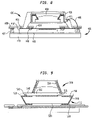
- FIG. 5 is an exploded view depicting a digital camera according to a further embodiment of the invention.
- FIG. 6 is a view similar to FIG. 5 , but depicting a digital camera according to yet another embodiment of the invention.
- FIG. 7 is a diagrammatic sectional view depicting a digital camera according to a further embodiment of the invention.
- FIG. 8 is a diagrammatic sectional view depicting a digital camera according to a still further embodiment of the invention.
- FIG. 9 is a view similar to FIG. 8 , but depicting a digital camera according to yet another embodiment of the invention.
- a camera module 10 ( FIG. 1 ) according to one embodiment of the invention includes an optoelectronic sensor 12 .
- the sensor has a body which includes a front surface 14 and an array of optically sensitive elements 16 such as CCD imaging cells arranged so that light impinging on the front surface 14 will pass to these optically sensitive elements.
- the sensor body includes a semiconductor chip 18 and a cover 20 which is transparent, at least in those regions aligned with optically sensitive elements 16 .
- Cover 20 typically is formed from glass or a transparent polymer. Cover 20 has an inner surface 22 facing toward chip 18 and an outer surface facing away from the chip, this outer surface constituting the front surface 14 of the sensor.
- a structure including a generally cylindrical, tubular container wall 26 projects from the outer surface 24 of cover 20 .
- Container wall 26 may be formed integrally with cover 20 , or may be assembled to the cover.
- the container wall 26 defines a generally cylindrical space 28 having an axis 30 which is aligned with the center of the array of sensing elements 16 .
- Chip 18 includes electrical circuitry schematically indicated at 32 connected to optically sensitive elements 16 for driving the sensitive elements and processing the signals from the sensitive elements into a desired form for output from the chip.
- circuitry 32 is arranged to actuate the actual charge coupled device cells cyclically and to read out the signals from the numerous cells in order, according to rows and/or columns.
- the circuitry is also arranged to convert these signals into digital form so that the output signals include a series or parallel data stream with digital bytes of information denoting the intensity of light received by the various pixels.
- the chip is a color imaging chip, the chip may include wavelength-sensitive filters on some or all cells, or may include cells having semiconductor elements sensitive to different wavelengths.
- references to “light” herein should be understood as including radiation in the ultraviolet and infrared ranges, as well as radiation in the visible range, unless otherwise specified.
- references to “optical”, elements should be understood as including elements suitable for use with ultraviolet or infrared radiation, as well as elements suitable for use with visible light.
- the circuitry of the chip is connected to contacts 34 , which, in this embodiment, are disposed on the front surface 36 of the chip, i.e., the surface bearing sensitive elements 16 and facing toward the cover 20 .
- Contacts 34 are electrically connected by through conductors 38 to electrical terminals 40 , referred to herein as “sensor terminals” exposed at the outer surface 14 of the cover.
- the through conductors 38 themselves may form a part or all of the terminals.
- a terminal “exposed at” a surface of a dielectric element may be flush with such surface; recessed relative to such surface; or protruding from such surface, so long as the terminal is accessible for contact by a theoretical point moving towards the surface in a direction perpendicular to the surface.
- the through conductors may include elements such as solid metallic spheres, solder connections or other metallic elements.
- sensor terminals 40 may be disposed at the same locations as through conductors 38 , or at different locations. Moreover, some of the sensor terminals may not be connected to contacts 34 , and some of the contacts 34 may be “dummy” terminals not to the internal circuitry 32 of the chip.
- the sensor also has additional terminals 41 exposed at the front surface 14 , these additional terminals 41 being referred to herein as “lens control” terminals.
- the lens control terminals 41 may or may not be connected to the internal circuitry of 32 of the sensor as explained below.
- Terminals 40 and 41 , and through conductors 38 desirably are disposed in peripheral regions of the chip and cover, outside of a central region enclosed by container wall 26 .
- a seal 44 extends between the cover 20 and semiconductor chip 18 .
- This seal may be formed in the same process as is used to apply the cover.
- the seal desirably extends around the entire periphery of the chip and cover.
- the through conductors and seal desirably are arranged so that the outer surface 14 of the cover is precisely parallel to the front surface 36 of the chip to within a close tolerance.
- Container wall 26 has a tapered portion 50 sloping inwardly towards axis 30 in the rearward or downward direction, towards chip 18 (the direction towards the bottom of the drawing as seen in FIG. 1 ).
- An electrode 52 covers the sloping portion 50 and extends around the entire periphery of the container.
- the electrode in turn, is covered by a dielectric coating 54 .
- Electrode 52 may be a discrete metallic element or may be a metallic or other conductive coating applied on the surface of the sloping wall portion 50 .
- Dielectric 54 most desirably is as thin as possible, while providing a pinhole-free dielectric coating having dielectric strength sufficient to withstand the voltages to be applied in service, typically on the order of a few hundred volts or less, as discussed below.
- the dielectric coating most preferably is a coating which is hydrophobic, i.e., which is not normally wetted by water.
- dielectric coating 54 may include a conformal coating, as, for example, a polyparaxylene or other vapor-deposited coating a few microns thick.
- the dielectric coating 54 may include a fluoropolymer or a polymer having a substantial preponderance of alkyl moieties at its surface.
- the dielectric coating includes a parylene-N coating covered by a fluoropolymer.
- a further electrode 56 is exposed to the interior of bore 28 at one end of the tapered section.
- the structure projecting from the sensor includes a closure 58 covering the end of bore 28 .
- the closure 58 is in the form of a rigid convex lens, but this feature is optional; the closure may be a simple planar element or another optical element such as a filter.
- the structure optionally includes a further support 60 extending forwardly from container wall 26 and closure 58 , and holding one or more additional optical elements such as a lens 62 .
- Liquid 64 disposed in contact with electrode 56 desirably is an aqueous, electrically conductive liquid such as a saline solution.
- Liquid 66 disposed in the rearward portion of bore 28 most preferably is a silicone oil such as a phenylated silicone oil.
- the two liquids most preferably have substantially equal specific gravity or density. The two liquids have different indices of refraction.
- the immiscible liquids cooperatively define a meniscus or curved interface 68 .
- meniscus 68 serves as a refractive interface which alters the focus of light passing through the bore 28 enroute to optically sensitive elements 16 .
- the nature and degree of this change will depend upon the curvature of the meniscus.
- the module 10 further includes a piezoelectric transformer 70 which, in this embodiment, is mounted to sensor 12 so that the transformer overlies the front surface 14 of the sensor.
- transformer 70 includes a primary piezoelectric element 72 and a secondary piezoelectric element 74 mechanically linked to the primary piezoelectric element so that deformation of the primary piezoelectric element 72 will cause deformation of the secondary piezoelectric element 74 .
- the two piezoelectric elements are directly connected to one another to form a body of piezoelectric material. In the transformer depicted in FIG.
- the body of piezoelectric material is depicted as a generally rectangular slab, with a thickness dimension (toward the top and bottom of the drawing) smaller than the length and width of the slab.
- the two elements have different poling directions.
- the primary piezoelectric element 72 has a poling direction corresponding to the thickness direction, as indicated by the vertical arrows in FIG. 3
- the secondary piezoelectric element 74 has a poling direction corresponding to the length of the slab, as indicated by the horizontal arrows.
- the term “poling” refers to the process of inducing a DC voltage across the material, so that ferroelectric domains of the material align to the induced field, and the term “poling direction” refers to the direction of the aligned domains after this process.
- the process of poling normally is performed during manufacture of the piezoelectric element.
- the piezoelectric material may be a ferroelectric ceramic such as such as lead zirconate titanate (PZT) or a polymeric piezoelectric material such as a polyvinylidene fluoride-trifluoroethylene copolymer.
- the primary piezoelectric element 72 has a primary ground electrode 76 and a primary signal electrode 78 disposed on opposite surfaces of the slab, so that the direction between these electrodes corresponds to the poling direction of the primary piezoelectric element.
- the secondary piezoelectric element 74 has a secondary signal electrode 80 disposed at one end of the slab, so that the secondary signal electrode is offset, in the poling direction of the secondary piezoelectric element, from the primary ground electrode 76 .
- the primary ground electrode 76 also serves as a ground electrode for the secondary piezoelectric element 74 ; in effect, the secondary element has electrodes 76 and 80 offset from one another in the poling direction of the secondary element.
- the primary piezoelectric element 72 grows or shrinks in the thickness direction of the slab, causing the entire slab, including the secondary piezoelectric element 74 , to grow or shrink in the lengthwise direction. This growth or shrinkage of the secondary piezoelectric element changes the electrical potential of the secondary signal electrode 80 with respect to the ground electrode 76 .
- the term “transformation ratio” means the absolute value of the ratio of the change in voltage appearing between the electrodes associated with the secondary piezoelectric element to the change in voltage applied between the electrodes of the primary piezoelectric element.
- piezoelectric transformers may have transformation ratios from less than one to thousands or more.
- the piezoelectric transformer most typically has a transformation ratio of about 10:1 or more, as, for example, about 10:1 to about 100:1.
- the particular form of piezoelectric transformer depicted in FIG. 3 is merely exemplary; other types of piezoelectric transformers can be employed.
- certain piezoelectric transformers have primary and secondary piezoelectric elements formed separately from one another and mechanically connected to one another by an intermediate element or linkage, so that deformation of the primary element is transmitted to the secondary element.
- the piezoelectric elements can be deformed in shear in bending, or in other modes, rather than in compression or tension.
- the piezoelectric elements may have essentially any shape.
- the primary ground electrode 76 is connected to the one of the lens control terminals 41 a ( FIG. 2 ), whereas primary signal electrode 78 is electrically connected to another lens control terminal 41 b , so that the primary piezoelectric element 72 is connected between these terminals.
- Terminal 41 a is referred to as the lens control ground terminal
- terminal 41 b is referred to as the lens control signal terminal.
- One of the control electrodes 52 of the variable optical element discussed above is connected to the secondary signal electrode 80
- the opposite control electrode 56 is electrically connected to the primary ground electrode, so that the control electrodes are electrically connected to the secondary piezoelectric element 74 .
- the shape of the meniscus 68 ( FIG. 1 ) is determined entirely by the wetting properties of the liquids, and accordingly may have a shape such as that shown at 68 in FIG. 1 .
- the aqueous liquid 64 becomes electrically charged with a voltage opposite to that prevailing on electrode 52 .
- the opposite charges in fluid 64 and on electrode 52 attract one another, thereby causing the aqueous liquid to extend further down the sloping wall 50 . Stated another way, the intersection between the meniscus and the sloping wall moves down the sloping wall.
- This action alters the shape of the meniscus and hence the shape of the refractive interface, so that the refractive interface has the configuration as shown in broken lines at 68 ′ in FIGS. 1 and 4 .
- the extent of this effect depends upon the applied voltage, so that by varying the voltage, the meniscus can be brought to intermediate shape between that shown in 68 ′ and that shown in solid lines at 68 . Because the shape of the refractive interface changes, the optical properties also change with the applied voltage.
- a maximum operating voltage on the order of 50-100 volts is used across electrodes 52 and 56 .
- the device operates by electrostatic attraction, it does not require a current flow during operation. From an electrical point of view, the device functions as a capacitor, with electrode 56 and aqueous fluid 64 constituting one plate, and with electrode 52 constituting the opposite plate.
- the piezoelectric voltage transformer 70 can supply the required voltage across electrodes 52 and 56 in response to a signal of a few volts or less applied between lens control signal terminal 41 b and lens control ground terminal 41 a.
- the camera module discussed above with reference to FIGS. 1-4 can be mounted readily on a circuit panel.
- the module is mounted on a circuit panel 90 having a rear surface 92 and an oppositely-facing front surface.
- the sensor terminals 40 and the lens control terminals 41 ( FIGS. 2 and 3 ) are engaged with and bonded to electrically conductive elements 94 exposed at the rear surface 92 of the circuit panel.
- the conductive elements of the circuit panel connect the sensor terminals 40 to signal processing elements and other circuits (not shown) of the digital camera, and connect the lens control terminals 41 to ground and to a source of a control signal voltage (not shown).
- This voltage source may be a manually-adjustable element as, for example, a potentiometer connected to a battery or other voltage source, or an automated element such as an automatic focusing circuit. Because the module includes transformer 70 , the external source of lens control voltage is only required to supply a relatively low voltage, as, for example, 0-5 volts. This limits the voltages which must be applied to the conductors of the circuit panel and hence simplifies the design of the circuit panel.
- Sensor 12 is disposed to the rear of the circuit panel (below the circuit panel as seen in FIG. 1 ).
- the front face 14 of the sensor faces forwardly, towards the circuit panel.
- the structure including the fluid container 26 and lenses 58 and 62 extends forward through a hole 96 in the circuit panel, so that at least a part of this structure is disposed in front of the circuit panel, i.e., above the circuit panel as seen in FIG. 1 . Stated another way, at least a part of the fluid container and lens structure is disposed on the opposite side of the circuit panel 90 from the optical sensor 12 .
- the piezoelectric transformer 70 also extends forwardly from the sensor 12 , and also projects through the circuit panel so that at least a part of the piezoelectric transformer is disposed in front of the circuit panel.
- the piezoelectric transformer projects forwardly from the sensor to a lesser extent than the fluid container and lens structure. Therefore, the piezoelectric transformer does not add to the overall height of the assembly.
- the piezoelectric transformer 70 overlies the sensor. Therefore, the transformer does not add to the overall area of the circuit panel 90 surfaces occupied by the sensor and optical elements. This embodiment thus provides a relatively compact, low-height mounting.
- the entire camera module 10 may be pre-assembled, handled, tested and stocked as a unit, and may be mounted to the circuit panel as a unit in a single operation.
- sensor terminals 40 and lens control terminals 41 are adapted for surface-mounting to the circuit panel.
- terminals 40 and 41 may include a solder or may be wettable by a solder, so that the entire module can be mounted to the circuit panel simply by solder-bonding the terminals to the pads of the circuit panel.
- Providing the voltage converter and the other elements of the variable focus lens and sensor in a single structure minimizes the number of components which must be handled, ordered and processed by the system's manufacturer. Additionally, this approach also permits testing of the complete assembly including the sensor and the variable focus lens, together with the voltage converter, prior to assembly with a circuit board or other circuit panel, thereby minimizing the need for rework of completed assemblies and improving outgoing product quality.
- meniscus 68 is the refractive interface closest to the front surface 14 of the sensor, and liquid 66 , which forms part of this refractive interface, is also in contact with the front surface 14 of the sensor. Therefore, light passing from refractive interface 68 passes through the liquid 66 to the front surface of the sensor without encountering any additional refractive interfaces.
- the use of a liquid extending from the refractive interface nearest the sensor to the sensor itself provides certain advantages.
- this arrangement reduces spurious reflections and glare in the image.
- the focusing effect of the optical system as a whole is enhanced by filling the space between refractive interface 68 and the front surface of the sensor.
- the camera module 10 discussed above with reference to FIGS. 1-4 may be fabricated by assembling the structure including container wall 26 , with or without additional optical element 62 and lens support 60 , to the sensor 12 so as to form a subassembly including the container wall structure and optoelectronic sensor, and assembling the piezoelectric transformer 70 with the other elements in the subassembly before mounting the resulting module to the circuit panel.
- the subassembly including the optoelectronic sensor and container wall structure and related elements can be mounted to the circuit panel, and the piezoelectric transformer 70 can be added thereafter.
- the piezoelectric transformer can be assembled to the optoelectronic sensor 12 to form a unit which can be held and stocked and subsequently united with the container structure and associated elements.
- a sensor module 100 ( FIG. 5 ) according to a further embodiment of the invention includes an optoelectronic sensor 112 similar to the sensor discussed above, together with a piezoelectric transformer 170 mounted to the sensor.
- a surface of the optoelectronic sensor in this case the front surface 114 defined by the cover 120 , has lens control terminals 141 and sensor terminals 140 .
- the front surface also has lens connection pads 102 and traces connected to these lens connection pads.
- the piezoelectric transformer is mounted on the optoelectronic sensor so that the primary piezoelectric element is connected to the lens control terminals 141 , whereas the signal electrode of the piezoelectric transformer is connected to one of the mounting pads 102 .
- the other mounting pad 102 is connected to the ground lens control terminal.
- This module can be assembled to a circuit panel 190 , such as a printed circuit board, with the sensor terminals 140 and lens control terminals 141 connected to conductive elements of the circuit panel, and with the piezoelectric transformer 170 projecting through a hole 195 in the printed circuit panel.
- the connection pads 102 and the optically sensitive elements 116 of the sensor are aligned with another hole 196 in the circuit panel.
- a structure 126 including a container and electrode similar to those discussed above is assembled through the hole 196 , so that the electrodes are connected to the mounting pads 102 .
- This structure 126 includes two transparent closures 158 and 159 so that it will retain the liquids constituting the meniscus 168 prior to assembly with the sensor.
- the complete camera module including structure 126 together with module 100 can be assembled prior to attachment to a printed circuit panel.
- both the container structure and the piezoelectric element 170 extend to the front of the circuit panel (above the circuit panel as seen in FIG. 5 ) and hence lie on the opposite side of the circuit panel from the sensor.
- a digital camera module 200 includes a sensor 212 , container and lens structure 226 , and piezoelectric transformer 270 supplied as separate components.
- the sensor includes mounting pads 202 for connection to the electrodes in the container and lens structure.
- the ground and primary signal electrodes of piezoelectric transformer 270 are electrically connected to two conductive elements 293 on the circuit panel, only one such conductive element being visible in FIG. 6 .
- Another conductive element 293 b is connected to the secondary signal electrode of the piezoelectric transformer 270 , but electrically isolated from other conductive elements on the circuit panel.
- That element 293 b carrying the signal from the secondary piezoelectric element, is electrically connected to a mounting pad 202 a by a trace 203 a on the sensor.
- Another mounting pad 202 b is connected by a further trace (not shown) to a conductive element of the circuit panel which carries a ground potential.
- Mounting pads 202 z and 202 b are connected to the control electrodes 252 and 258 associated with the meniscus.
- only a portion of piezoelectric transformer 270 overlies sensor 212 ; another portion of the piezoelectric transformer projects beyond the edge of the sensor. Nonetheless, the assembly saves space by placing at least a portion of the piezoelectric transformer in alignment with the sensor 212 , using space which would otherwise be wasted.
- a camera 300 includes a preformed variable optical module 305 .
- This module incorporates the container structure 326 holding the electrodes 352 , 358 , and the liquids which define the meniscus 368 .
- Module 305 also includes a piezoelectric transformer 370 mounted to structure 326 .
- the piezoelectric transformer 370 has a primary signal terminal 380 connected to the primary signal electrode and a ground terminal 381 connected to the primary ground electrode.
- the transformer is mounted to the container structure 326 so that these terminals are exposed for connection to conductive elements 393 of the circuit panel.
- the variable optical element assembly 305 further includes a conductor shown schematically at 371 connecting the secondary signal electrode of transformer 370 to one electrode 352 used to control the meniscus 368 and another conductor 373 connecting the opposite meniscus-control electrode 358 to the ground terminal 381 of the transformer.
- the container structure 326 itself may have ground and primary signal terminals exposed for connection to the circuit panel, and the ground and primary signal electrodes of the transformer may be connected to these terminals.
- Structure 326 may include elements other than the container itself as, for example, appropriate brackets or projections for mounting and supporting the structure 326 itself, and for mounting the piezoelectric transformer 370 . Structure 326 may also include additional optical elements (not shown).
- the optoelectronic sensor 312 is mounted so that the sensor overlies the rear surface 392 of the circuit panel 390 .
- Structure 326 has projecting features 307 which extend through openings 395 in the circuit panel and engage the front face 314 of the sensor, so as to hold structure 326 in accurate positional relationship with the sensor.
- the structure 326 may incorporate positioning features 307 similar to the features disclosed in copending commonly assigned U.S. Published Patent Application Nos. 2005/0248680, published Nov. 10, 2005; and 2006/0109366, published May 25, 2006, the disclosures of which are hereby incorporated by reference herein.
- the preformed optical module 305 may be handled and stocked as a unit, and may be united with the optoelectronic sensor 312 before, after or during assembly of the sensor 312 to the circuit panel.
- the preformed optical module thus provides additional flexibility in manufacturing; the same assembly can be used with different types of sensors. Also, there is no need for special configuration of the sensor to work with the module.
- a sensor module 400 according to yet another embodiment of the invention includes a preformed sensor module 405 which incorporates the piezoelectric transformer 470 and the optoelectronic sensor 412 .
- transformer 470 overlies the rear surface of the sensor 412 , i.e., the surface of the sensor opposite from the surface having the optically sensitive elements 416 .
- the sensor 412 does not incorporate a separate cover, but instead incorporates a transparent passivation layer 401 defining the front surface 414 of the sensor.
- Module 405 further includes a module substrate 403 . Optoelectronic sensor 412 and piezoelectric transformer 470 are mounted to module substrate 403 .
- the module substrate 403 has electrical connecting elements 407 projecting from the module substrate at one or more locations outside of the area occupied by the sensor 412 . These electrical connecting elements are electrically connected to the piezoelectric transformer 470 by appropriate interconnections (not shown), as for example, by traces carried on module substrate 403 and features such as wire bonds or solder bonds connecting the traces to the electrodes of the piezoelectric transformer. Connecting elements 407 are exposed for connection to a circuit panel and serve as lens control terminals of module 405 . The terminals of sensor 412 are also exposed for connection to the circuit panel and form the sensor terminals of the module.
- the piezoelectric transformer 470 and optoelectronic sensor 412 optionally may be adhesively bonded to the module substrate 403 or secured to the module substrate by soldering. Also, one or more electrical connections to the sensor may be made through the conductive elements 407 and associated traces or other electrical elements on the module substrate, so that connecting elements 407 also serve as sensor terminals of the module.
- Module 405 may be mounted to the rear side of a circuit panel 490 .
- the structure 426 holding the electrodes and fluids associated with the adjustable meniscus 468 overlies the front surface of the circuit panel, but rests on the front surface 414 of the sensor to maintain alignment.
- the electrical conductor 407 carrying the signal from the piezoelectric transformer is electrically connected through the circuit panel, as for example, a wire bond 409 extending to a pad 411 on structure 426 electrically connected to the signal electrode.
- the ground electrode can be similarly connected to the piezoelectric transformer or to a ground conductor (not shown) on circuit panel 490 . This arrangement provides a particularly large space for the transformer; the transformer may occupy a greater surface area than the optoelectronic sensor 412 .
- the camera module of FIG. 8 may be fabricated by assembling the sensor module 405 incorporating sensor 412 , substrate 403 , and transformer 470 to the circuit panel and subsequently mounting structure 426 to the circuit panel and module.
- the module which includes the sensor and piezoelectric transformer also has the structure 426 carrying the meniscus fluids and electrodes mounted thereon prior to assembly of the module with the circuit panel.
- module 405 has no substrate 403 .
- transformer 470 may be fastened directly to sensor 412 .
- a digital camera 500 includes a subassembly incorporating a sensor 512 and a structure 526 for holding the fluids defining the meniscus.
- Sensor 512 includes a semiconductor chip 518 having sensitive elements 516 on a chip front surface 536 .
- Chip 518 has “wraparound” leads 538 which extend from the chip front surface to terminals 540 on the opposite, rear surface 539 of the chip.
- the sensor includes a cover 520 or a passivation layer forming the front surface of the sensor.
- the container structure 526 includes a self-supporting metallic structure with the dielectric layer or coating 554 covering the entire interior surface of this structure.
- container structure 526 serves in its entirety as one of the electrodes.
- the electrode 556 is provided as a flat metallic ring on the front surface of the sensor. Also, in this arrangement, the electrically conductive liquid 564 lies closest to the sensor, whereas the non-conductive liquid or oil 566 lies remote from the sensor, on the opposite side of meniscus 568 . Electrode 556 is electrically isolated from electrode 526 , but is connected to one or more of the wraparound leads 538 , as, for example, by a trace 542 and a through conductor 543 extending through the cover. The opposite electrode 526 may be connected to one of the wraparound electrodes 538 in a similar manner.
- one or both of the electrodes may be connected to specialized wraparound leads which extend onto the outer surface 524 of the cover, rather than between the cover and chip 518 , as depicted in FIG. 9 .
- the other wraparound leads are connected to the internal circuitry (not shown) within sensor 512 .
- Chips with wraparound leads of this type are known in the art; such chips are disclosed, for example, in U.S. Pat. No. 6,646,289 and, therefore, are not described further herein.
- the subassembly can be mounted in a face-up configuration, with container 526 pointing away from a circuit panel, as, for example, by surface-mounting terminals 540 on the front surface 592 of a circuit panel 590 .
- the camera module further includes a piezoelectric transformer 570 mounted to the rear of the circuit panel. In this configuration as well, at least a part of the piezoelectric transformer 570 is aligned with the sensor 512 in the horizontal directions, parallel to the plane of the circuit panel.
- the configuration of the container depicted in FIG. 9 with a solid, self-supporting metal wall can be used in the other embodiments discussed above.
- the container 526 can incorporate a dielectric wall with a metallic conductive layer as shown, for example, in FIG. 1 .
- the piezoelectric transformer can be mounted to the container structure 526 or to the sensor 512 in a face-up embodiment of the type depicted in FIG. 9 .
- a sensor incorporating a cover as depicted in FIG. 1 can be substituted for the sensor shown in FIG. 8 , which omits the cover, and vice-versa.
- the piezoelectric transformer it is not essential to mount the piezoelectric transformer in alignment with the sensor; if available space on a circuit panel permits, the piezoelectric transformer can be mounted in any location. Also, it is not essential to place parts of the assembly on opposite sides of a circuit panel; all of the components may lie on one side of the circuit panel. Indeed, the camera need not incorporate a circuit panel at all.
- the camera may include a multiplicity of refractive meniscus interfaces in series, as, for example, a layer of an aqueous liquid forming a first meniscus with a layer of an oil immiscible with the first liquid, followed by a layer of a third liquid which is immiscible with the wall and desirably also immiscible with the aqueous liquid.
- These may be driven by the same piezoelectric transformer or by a plurality of transformers, at least one of which is a piezoelectric transformer.
- the optical module including the lens and piezoelectric transformer may be used by itself or with devices other than an optoelectronic sensor as, for example, in a film-based camera or other optical instrument.
- a sensor module or subcombination incorporating an optoelectronic sensor and a piezoelectric transformer may be used as a component of a digital camera.
- elements which are referred to herein as “connected” to one another, “attached” to one another, “mounted” to one another in those terms or in terms of similar meaning need not be directly connected, mounted or attached to one another, but may also be connected, mounted or attached to one another through intermediate structures intervening between the specified elements.
Landscapes
- Physics & Mathematics (AREA)
- Engineering & Computer Science (AREA)
- General Physics & Mathematics (AREA)
- Multimedia (AREA)
- Signal Processing (AREA)
- Power Engineering (AREA)
- Optics & Photonics (AREA)
- Electromagnetism (AREA)
- Condensed Matter Physics & Semiconductors (AREA)
- Computer Hardware Design (AREA)
- Microelectronics & Electronic Packaging (AREA)
- Studio Devices (AREA)
Abstract
Description
Claims (21)
Priority Applications (1)
| Application Number | Priority Date | Filing Date | Title |
|---|---|---|---|
| US11/318,821 US7443597B2 (en) | 2005-12-27 | 2005-12-27 | Liquid lens with piezoelectric voltage converter |
Applications Claiming Priority (1)
| Application Number | Priority Date | Filing Date | Title |
|---|---|---|---|
| US11/318,821 US7443597B2 (en) | 2005-12-27 | 2005-12-27 | Liquid lens with piezoelectric voltage converter |
Publications (2)
| Publication Number | Publication Date |
|---|---|
| US20070146894A1 US20070146894A1 (en) | 2007-06-28 |
| US7443597B2 true US7443597B2 (en) | 2008-10-28 |
Family
ID=38193368
Family Applications (1)
| Application Number | Title | Priority Date | Filing Date |
|---|---|---|---|
| US11/318,821 Expired - Fee Related US7443597B2 (en) | 2005-12-27 | 2005-12-27 | Liquid lens with piezoelectric voltage converter |
Country Status (1)
| Country | Link |
|---|---|
| US (1) | US7443597B2 (en) |
Cited By (23)
| Publication number | Priority date | Publication date | Assignee | Title |
|---|---|---|---|---|
| US20070147816A1 (en) * | 2005-12-27 | 2007-06-28 | Tessera, Inc. | Camera modules with liquid optical elements |
| US20080282574A1 (en) * | 2003-12-22 | 2008-11-20 | Elke Zakel | Method and Device For Drying Circuit Substrates |
| US20100243862A1 (en) * | 2009-03-31 | 2010-09-30 | Laurens Nunnink | System for adjusting focus of a liquid lens in a machine vision system |
| WO2014033099A2 (en) | 2012-08-27 | 2014-03-06 | Digital Optics Corporation Europe Limited | Rearview imaging systems for vehicle |
| WO2014072837A2 (en) | 2012-06-07 | 2014-05-15 | DigitalOptics Corporation Europe Limited | Mems fast focus camera module |
| US9001268B2 (en) | 2012-08-10 | 2015-04-07 | Nan Chang O-Film Optoelectronics Technology Ltd | Auto-focus camera module with flexible printed circuit extension |
| US9007520B2 (en) | 2012-08-10 | 2015-04-14 | Nanchang O-Film Optoelectronics Technology Ltd | Camera module with EMI shield |
| US9091843B1 (en) | 2014-03-16 | 2015-07-28 | Hyperion Development, LLC | Optical assembly for a wide field of view point action camera with low track length to focal length ratio |
| US9316820B1 (en) | 2014-03-16 | 2016-04-19 | Hyperion Development, LLC | Optical assembly for a wide field of view point action camera with low astigmatism |
| US9316808B1 (en) | 2014-03-16 | 2016-04-19 | Hyperion Development, LLC | Optical assembly for a wide field of view point action camera with a low sag aspheric lens element |
| US9443291B2 (en) | 2013-06-20 | 2016-09-13 | Samsung Electronics Co., Ltd. | Methods for lens calibration and image restoration |
| US9494772B1 (en) | 2014-03-16 | 2016-11-15 | Hyperion Development, LLC | Optical assembly for a wide field of view point action camera with low field curvature |
| US9525807B2 (en) | 2010-12-01 | 2016-12-20 | Nan Chang O-Film Optoelectronics Technology Ltd | Three-pole tilt control system for camera module |
| US9575221B2 (en) | 2013-12-31 | 2017-02-21 | Cognex Corporation | Systems and methods reduce temperature induced drift effects on a liquid lens |
| US9726859B1 (en) | 2014-03-16 | 2017-08-08 | Navitar Industries, Llc | Optical assembly for a wide field of view camera with low TV distortion |
| US9995910B1 (en) | 2014-03-16 | 2018-06-12 | Navitar Industries, Llc | Optical assembly for a compact wide field of view digital camera with high MTF |
| WO2018140697A1 (en) | 2017-01-26 | 2018-08-02 | Navitar, Inc. | High etendue modular zoom lens for machine vision |
| US10101636B2 (en) | 2012-12-31 | 2018-10-16 | Digitaloptics Corporation | Auto-focus camera module with MEMS capacitance estimator |
| US10139595B1 (en) | 2014-03-16 | 2018-11-27 | Navitar Industries, Llc | Optical assembly for a compact wide field of view digital camera with low first lens diameter to image diagonal ratio |
| US10386604B1 (en) | 2014-03-16 | 2019-08-20 | Navitar Industries, Llc | Compact wide field of view digital camera with stray light impact suppression |
| CN110661954A (en) * | 2019-10-14 | 2020-01-07 | Oppo广东移动通信有限公司 | Camera module and terminal equipment |
| US10545314B1 (en) | 2014-03-16 | 2020-01-28 | Navitar Industries, Llc | Optical assembly for a compact wide field of view digital camera with low lateral chromatic aberration |
| US10690816B2 (en) | 2013-12-31 | 2020-06-23 | Cognex Corporation | Systems and methods reduce temperature induced drift effects on a liquid lens |
Families Citing this family (16)
| Publication number | Priority date | Publication date | Assignee | Title |
|---|---|---|---|---|
| US7576401B1 (en) | 2005-07-07 | 2009-08-18 | Amkor Technology, Inc. | Direct glass attached on die optical module |
| JP2009186596A (en) * | 2008-02-04 | 2009-08-20 | Sony Corp | Imaging lens system and imaging apparatus using the same |
| TWI368098B (en) * | 2008-03-27 | 2012-07-11 | E Pin Optical Industry Co Ltd | Electromagnet for lens driving mechanism thereof |
| US20100025793A1 (en) * | 2008-08-01 | 2010-02-04 | Impac Technology Co., Ltd. | Assembly for image sensing chip and assembling method thereof |
| JP2010054864A (en) * | 2008-08-28 | 2010-03-11 | Sony Corp | Liquid lens element and lighting system |
| US8385885B2 (en) * | 2008-10-17 | 2013-02-26 | Sony Ericsson Mobile Communications Ab | Method of unlocking a mobile electronic device |
| US8282004B2 (en) * | 2009-04-29 | 2012-10-09 | Hand Held Products, Inc. | Focusing apparatus and terminal comprising variable focus lens assembly |
| KR20110064156A (en) * | 2009-12-07 | 2011-06-15 | 삼성전자주식회사 | Imaging device and its manufacturing method |
| US8260129B2 (en) * | 2009-12-23 | 2012-09-04 | Varioptic, S.A. | Optical device for high quality and compact camera module |
| DE102010018921A1 (en) * | 2010-04-30 | 2011-11-03 | Conti Temic Microelectronic Gmbh | Camera module with image recording element for a motor vehicle |
| US8866246B2 (en) * | 2012-11-01 | 2014-10-21 | Larview Technologies Corporation | Holder on chip module structure |
| US20190293898A1 (en) * | 2016-03-18 | 2019-09-26 | Sumitomo Electric Industries, Ltd. | Infrared lens unit |
| CN206946171U (en) * | 2016-07-14 | 2018-01-30 | 三星电机株式会社 | Transparency window cleaning device and the camera apparatus for being equipped with transparency window cleaning device |
| KR102543699B1 (en) * | 2018-01-23 | 2023-06-13 | 엘지이노텍 주식회사 | Liquid len module, lens assembly including the module, and camera module including the assembly |
| CN110441902A (en) * | 2019-08-08 | 2019-11-12 | 上海酷聚科技有限公司 | A kind of liquid lens and preparation method thereof |
| CN110730285B (en) * | 2019-10-14 | 2021-07-09 | Oppo广东移动通信有限公司 | Camera module and terminal equipment |
Citations (23)
| Publication number | Priority date | Publication date | Assignee | Title |
|---|---|---|---|---|
| US5091801A (en) * | 1989-10-19 | 1992-02-25 | North East Research Associates, Inc. | Method and apparatus for adjusting the focal length of a optical system |
| US6538823B2 (en) | 2001-06-19 | 2003-03-25 | Lucent Technologies Inc. | Tunable liquid microlens |
| US6545815B2 (en) | 2001-09-13 | 2003-04-08 | Lucent Technologies Inc. | Tunable liquid microlens with lubrication assisted electrowetting |
| US6545816B1 (en) | 2001-10-19 | 2003-04-08 | Lucent Technologies Inc. | Photo-tunable liquid microlens |
| US6618208B1 (en) | 1998-03-19 | 2003-09-09 | Joshua David Silver | Variable focus optical devices |
| US6646289B1 (en) | 1998-02-06 | 2003-11-11 | Shellcase Ltd. | Integrated circuit device |
| US6665127B2 (en) | 2002-04-30 | 2003-12-16 | Lucent Technologies Inc. | Method and apparatus for aligning a photo-tunable microlens |
| US6747806B2 (en) | 2001-04-19 | 2004-06-08 | Creo Srl | Method for controlling light beam using adaptive micro-lens |
| US6778328B1 (en) | 2003-03-28 | 2004-08-17 | Lucent Technologies Inc. | Tunable field of view liquid microlens |
| US20050002112A1 (en) | 2001-06-19 | 2005-01-06 | Kroupenkine Timofei Nikita | Method and apparatus for calibrating a tunable microlens |
| US20050082653A1 (en) | 2003-09-26 | 2005-04-21 | Tessera, Inc. | Structure and method of making sealed capped chips |
| US6891682B2 (en) | 2003-03-03 | 2005-05-10 | Lucent Technologies Inc. | Lenses with tunable liquid optical elements |
| US20050113912A1 (en) | 2002-02-14 | 2005-05-26 | Koninklijke Philips Electronics N. V. | Variable focus lens |
| US6909555B2 (en) * | 1995-06-07 | 2005-06-21 | Jacob N. Wohlstadter | Three dimensional imaging system |
| US6936196B2 (en) | 2002-03-12 | 2005-08-30 | Lucent Technologies Inc. | Solidifiable tunable liquid microlens |
| US6961187B2 (en) | 2001-09-21 | 2005-11-01 | Olympus Corporation | Imaging device |
| US20050248680A1 (en) | 2004-05-04 | 2005-11-10 | Tessera, Inc. | Compact lens turret assembly |
| US6977777B1 (en) | 2004-06-18 | 2005-12-20 | Sandia Corporation | Active optical zoom system |
| US6989626B2 (en) | 2001-09-28 | 2006-01-24 | Matsushita Electric Industrial Co., Ltd. | Piezoelectric transformer |
| US20060028734A1 (en) * | 2002-10-25 | 2006-02-09 | Koninklijke Philips Electronics, N.V. | Zoom Lens |
| US20060072070A1 (en) | 2002-12-03 | 2006-04-06 | Koninklijke Philips Electronics N.V. | Manufacturing of lens elements |
| US7046447B2 (en) * | 2003-01-13 | 2006-05-16 | Pc Mirage, Llc | Variable focus system |
| US20060109366A1 (en) | 2004-05-04 | 2006-05-25 | Tessera, Inc. | Compact lens turret assembly |
-
2005
- 2005-12-27 US US11/318,821 patent/US7443597B2/en not_active Expired - Fee Related
Patent Citations (27)
| Publication number | Priority date | Publication date | Assignee | Title |
|---|---|---|---|---|
| US5091801A (en) * | 1989-10-19 | 1992-02-25 | North East Research Associates, Inc. | Method and apparatus for adjusting the focal length of a optical system |
| US6909555B2 (en) * | 1995-06-07 | 2005-06-21 | Jacob N. Wohlstadter | Three dimensional imaging system |
| US6646289B1 (en) | 1998-02-06 | 2003-11-11 | Shellcase Ltd. | Integrated circuit device |
| US6618208B1 (en) | 1998-03-19 | 2003-09-09 | Joshua David Silver | Variable focus optical devices |
| US6747806B2 (en) | 2001-04-19 | 2004-06-08 | Creo Srl | Method for controlling light beam using adaptive micro-lens |
| US20050088754A9 (en) | 2001-06-19 | 2005-04-28 | Kroupenkine Timofei N. | Method and apparatus for calibrating a tunable microlens |
| US6538823B2 (en) | 2001-06-19 | 2003-03-25 | Lucent Technologies Inc. | Tunable liquid microlens |
| US6965480B2 (en) | 2001-06-19 | 2005-11-15 | Lucent Technologies Inc. | Method and apparatus for calibrating a tunable microlens |
| US20050002112A1 (en) | 2001-06-19 | 2005-01-06 | Kroupenkine Timofei Nikita | Method and apparatus for calibrating a tunable microlens |
| US6545815B2 (en) | 2001-09-13 | 2003-04-08 | Lucent Technologies Inc. | Tunable liquid microlens with lubrication assisted electrowetting |
| US6961187B2 (en) | 2001-09-21 | 2005-11-01 | Olympus Corporation | Imaging device |
| US6989626B2 (en) | 2001-09-28 | 2006-01-24 | Matsushita Electric Industrial Co., Ltd. | Piezoelectric transformer |
| US6545816B1 (en) | 2001-10-19 | 2003-04-08 | Lucent Technologies Inc. | Photo-tunable liquid microlens |
| US20050113912A1 (en) | 2002-02-14 | 2005-05-26 | Koninklijke Philips Electronics N. V. | Variable focus lens |
| US6936196B2 (en) | 2002-03-12 | 2005-08-30 | Lucent Technologies Inc. | Solidifiable tunable liquid microlens |
| US6665127B2 (en) | 2002-04-30 | 2003-12-16 | Lucent Technologies Inc. | Method and apparatus for aligning a photo-tunable microlens |
| US20060028734A1 (en) * | 2002-10-25 | 2006-02-09 | Koninklijke Philips Electronics, N.V. | Zoom Lens |
| US20060072070A1 (en) | 2002-12-03 | 2006-04-06 | Koninklijke Philips Electronics N.V. | Manufacturing of lens elements |
| US7046447B2 (en) * | 2003-01-13 | 2006-05-16 | Pc Mirage, Llc | Variable focus system |
| US6891682B2 (en) | 2003-03-03 | 2005-05-10 | Lucent Technologies Inc. | Lenses with tunable liquid optical elements |
| US6778328B1 (en) | 2003-03-28 | 2004-08-17 | Lucent Technologies Inc. | Tunable field of view liquid microlens |
| US20050095835A1 (en) | 2003-09-26 | 2005-05-05 | Tessera, Inc. | Structure and method of making capped chips having vertical interconnects |
| US20050082653A1 (en) | 2003-09-26 | 2005-04-21 | Tessera, Inc. | Structure and method of making sealed capped chips |
| US20050082654A1 (en) | 2003-09-26 | 2005-04-21 | Tessera, Inc. | Structure and self-locating method of making capped chips |
| US20050248680A1 (en) | 2004-05-04 | 2005-11-10 | Tessera, Inc. | Compact lens turret assembly |
| US20060109366A1 (en) | 2004-05-04 | 2006-05-25 | Tessera, Inc. | Compact lens turret assembly |
| US6977777B1 (en) | 2004-06-18 | 2005-12-20 | Sandia Corporation | Active optical zoom system |
Non-Patent Citations (8)
| Title |
|---|
| Humpston et al, U.S. Appl. No. 11/318,874, filed Dec. 27, 2005, entitled "Camera Modules With Liquid Optical Elements." |
| Kuiper, Hendriks, "Through a lens sharply," Spectrum IEEE, Dec. 2004 edition http://www.spectrum.ieee.org/print/4172. |
| Stein Kuiper & Benno Hendriks, "Wet & Wild-Liquid Lenses Provide Quality Images For Camera Phones," SPIE's oemagazine, Jan. 2005. |
| T. Krupenkin, S. Yang, and P. Mach, "Tunable liquid microlens," Applied Physics Letters, Jan. 20, 2003, vol. 82, Issue 3, pp. 316-318. |
| U.S. Appl. No. 10/949,746. |
| U.S. Appl. No. 10/949,764. |
| U.S. Appl. No. 11/121,434. |
| U.S. Appl. No. 11/265,727. |
Cited By (42)
| Publication number | Priority date | Publication date | Assignee | Title |
|---|---|---|---|---|
| US20080282574A1 (en) * | 2003-12-22 | 2008-11-20 | Elke Zakel | Method and Device For Drying Circuit Substrates |
| US8256131B2 (en) * | 2003-12-22 | 2012-09-04 | Pac-Tech—Packaging Technologies GmbH | Method and device for drying circuit substrates |
| US20070147816A1 (en) * | 2005-12-27 | 2007-06-28 | Tessera, Inc. | Camera modules with liquid optical elements |
| US20100243862A1 (en) * | 2009-03-31 | 2010-09-30 | Laurens Nunnink | System for adjusting focus of a liquid lens in a machine vision system |
| US8487228B2 (en) | 2009-03-31 | 2013-07-16 | Cognex Corporation | System for adjusting focus of a liquid lens in a machine vision system |
| US9525807B2 (en) | 2010-12-01 | 2016-12-20 | Nan Chang O-Film Optoelectronics Technology Ltd | Three-pole tilt control system for camera module |
| WO2014072837A2 (en) | 2012-06-07 | 2014-05-15 | DigitalOptics Corporation Europe Limited | Mems fast focus camera module |
| US9007520B2 (en) | 2012-08-10 | 2015-04-14 | Nanchang O-Film Optoelectronics Technology Ltd | Camera module with EMI shield |
| US9001268B2 (en) | 2012-08-10 | 2015-04-07 | Nan Chang O-Film Optoelectronics Technology Ltd | Auto-focus camera module with flexible printed circuit extension |
| WO2014033099A2 (en) | 2012-08-27 | 2014-03-06 | Digital Optics Corporation Europe Limited | Rearview imaging systems for vehicle |
| US10101636B2 (en) | 2012-12-31 | 2018-10-16 | Digitaloptics Corporation | Auto-focus camera module with MEMS capacitance estimator |
| US9443291B2 (en) | 2013-06-20 | 2016-09-13 | Samsung Electronics Co., Ltd. | Methods for lens calibration and image restoration |
| US10690816B2 (en) | 2013-12-31 | 2020-06-23 | Cognex Corporation | Systems and methods reduce temperature induced drift effects on a liquid lens |
| US10754071B2 (en) | 2013-12-31 | 2020-08-25 | Cognex Corporation | Systems and methods reduce temperature induced drift effects on a liquid lens |
| US11681081B2 (en) | 2013-12-31 | 2023-06-20 | Cognex Corporation | Systems and methods to reduce temperature induced drift effects on a liquid lens |
| US11754755B2 (en) | 2013-12-31 | 2023-09-12 | Cognex Corporation | Systems and methods to reduce temperature induced drift effects on a liquid lens |
| US9575221B2 (en) | 2013-12-31 | 2017-02-21 | Cognex Corporation | Systems and methods reduce temperature induced drift effects on a liquid lens |
| US9726859B1 (en) | 2014-03-16 | 2017-08-08 | Navitar Industries, Llc | Optical assembly for a wide field of view camera with low TV distortion |
| US10386604B1 (en) | 2014-03-16 | 2019-08-20 | Navitar Industries, Llc | Compact wide field of view digital camera with stray light impact suppression |
| US9995910B1 (en) | 2014-03-16 | 2018-06-12 | Navitar Industries, Llc | Optical assembly for a compact wide field of view digital camera with high MTF |
| US9778444B1 (en) | 2014-03-16 | 2017-10-03 | Navitar Industries, Llc | Optical assembly for a wide field of view point action camera with low astigmatism |
| US10739561B1 (en) | 2014-03-16 | 2020-08-11 | Navitar Industries, Llc | Optical assembly for a compact wide field of view digital camera with high MTF |
| US10107989B1 (en) | 2014-03-16 | 2018-10-23 | Navitar Industries, Llc | Optical assembly for a wide field of view point action camera with low field curvature |
| US10139595B1 (en) | 2014-03-16 | 2018-11-27 | Navitar Industries, Llc | Optical assembly for a compact wide field of view digital camera with low first lens diameter to image diagonal ratio |
| US10139599B1 (en) | 2014-03-16 | 2018-11-27 | Navitar Industries, Llc | Optical assembly for a wide field of view camera with low TV distortion |
| US10317652B1 (en) | 2014-03-16 | 2019-06-11 | Navitar Industries, Llc | Optical assembly for a wide field of view point action camera with low astigmatism |
| US9784943B1 (en) | 2014-03-16 | 2017-10-10 | Navitar Industries, Llc | Optical assembly for a wide field of view point action camera with a low sag aspheric lens element |
| US11754809B2 (en) | 2014-03-16 | 2023-09-12 | Navitar, Inc. | Optical assembly for a wide field of view point action camera with low field curvature |
| US10545314B1 (en) | 2014-03-16 | 2020-01-28 | Navitar Industries, Llc | Optical assembly for a compact wide field of view digital camera with low lateral chromatic aberration |
| US10545313B1 (en) | 2014-03-16 | 2020-01-28 | Navitar Industries, Llc | Optical assembly for a wide field of view point action camera with a low sag aspheric lens element |
| US9494772B1 (en) | 2014-03-16 | 2016-11-15 | Hyperion Development, LLC | Optical assembly for a wide field of view point action camera with low field curvature |
| US9316808B1 (en) | 2014-03-16 | 2016-04-19 | Hyperion Development, LLC | Optical assembly for a wide field of view point action camera with a low sag aspheric lens element |
| US9316820B1 (en) | 2014-03-16 | 2016-04-19 | Hyperion Development, LLC | Optical assembly for a wide field of view point action camera with low astigmatism |
| US10746967B2 (en) | 2014-03-16 | 2020-08-18 | Navitar Industries, Llc | Optical assembly for a wide field of view point action camera with low field curvature |
| US9091843B1 (en) | 2014-03-16 | 2015-07-28 | Hyperion Development, LLC | Optical assembly for a wide field of view point action camera with low track length to focal length ratio |
| WO2018140697A1 (en) | 2017-01-26 | 2018-08-02 | Navitar, Inc. | High etendue modular zoom lens for machine vision |
| US10678032B2 (en) | 2017-01-26 | 2020-06-09 | Navitar, Inc. | High etendue modular zoom lens for machine vision having five lens groups |
| US10670842B2 (en) | 2017-01-26 | 2020-06-02 | Navitar, Inc. | High Etendue zoom lens having five lens groups |
| US10914928B2 (en) | 2017-01-26 | 2021-02-09 | Navitar, Inc. | Rear adapter for a high etendue modular zoom lens |
| US10670844B2 (en) | 2017-01-26 | 2020-06-02 | Navitar, Inc. | High etendue modular lens assembly with afocal zoom having five lens groups |
| US10670843B2 (en) | 2017-01-26 | 2020-06-02 | Navitar, Inc. | High etendue lens assembly with large zoom range |
| CN110661954A (en) * | 2019-10-14 | 2020-01-07 | Oppo广东移动通信有限公司 | Camera module and terminal equipment |
Also Published As
| Publication number | Publication date |
|---|---|
| US20070146894A1 (en) | 2007-06-28 |
Similar Documents
| Publication | Publication Date | Title |
|---|---|---|
| US7443597B2 (en) | Liquid lens with piezoelectric voltage converter | |
| US20070147816A1 (en) | Camera modules with liquid optical elements | |
| US11240414B2 (en) | Camera module having a slim overall structure and portable device comprising same | |
| US11601576B2 (en) | Array camera module having height difference, circuit board assembly and manufacturing method therefor, and electronic device | |
| EP3790268B1 (en) | Camera module | |
| US7768713B2 (en) | Liquid lens and lens module having same | |
| CA2654422C (en) | Camera module with premolded lens housing and method of manufacture | |
| US8107005B2 (en) | Method of manufacturing an image sensor module | |
| US20090015706A1 (en) | Auto focus/zoom modules using wafer level optics | |
| US20060164539A1 (en) | Camera module, camera system and method of manufacturing a camera module | |
| KR20080094105A (en) | Integrated lens system for image sensor and method for manufacturing the same | |
| US20120170923A1 (en) | Camera module and method for manufacturing the same | |
| KR100596104B1 (en) | Cmos image sensor | |
| US20080142917A1 (en) | Image sensor module, method of manufacturing the same, and camera module having the same | |
| US20090194668A1 (en) | Image sensor module, camera module including the same and electronic device including the camera module | |
| CN100354675C (en) | Optical system and imaging device | |
| KR102449848B1 (en) | Lens driving equipment and information and technology equipment including the same | |
| CN114077028A (en) | Vertical zoom module and corresponding shooting method | |
| EP3575856B1 (en) | Liquid lens module and camera module comprising same | |
| CN113424514B (en) | Camera module including liquid lens and control method thereof | |
| KR102072775B1 (en) | Camera module | |
| US20040179249A1 (en) | Simplified image sensor module | |
| KR100795181B1 (en) | Camera module pakage and assembly method thereof | |
| KR20210088975A (en) | Sensing device | |
| CN115469386A (en) | Liquid lens and camera module |
Legal Events
| Date | Code | Title | Description |
|---|---|---|---|
| AS | Assignment |
Owner name: TESSERA, INC., CALIFORNIA Free format text: ASSIGNMENT OF ASSIGNORS INTEREST;ASSIGNOR:HUMPSTON, GILES;REEL/FRAME:017306/0694 Effective date: 20060224 |
|
| STCF | Information on status: patent grant |
Free format text: PATENTED CASE |
|
| CC | Certificate of correction | ||
| FPAY | Fee payment |
Year of fee payment: 4 |
|
| FPAY | Fee payment |
Year of fee payment: 8 |
|
| AS | Assignment |
Owner name: ROYAL BANK OF CANADA, AS COLLATERAL AGENT, CANADA Free format text: SECURITY INTEREST;ASSIGNORS:INVENSAS CORPORATION;TESSERA, INC.;TESSERA ADVANCED TECHNOLOGIES, INC.;AND OTHERS;REEL/FRAME:040797/0001 Effective date: 20161201 |
|
| AS | Assignment |
Owner name: BANK OF AMERICA, N.A., NORTH CAROLINA Free format text: SECURITY INTEREST;ASSIGNORS:ROVI SOLUTIONS CORPORATION;ROVI TECHNOLOGIES CORPORATION;ROVI GUIDES, INC.;AND OTHERS;REEL/FRAME:053468/0001 Effective date: 20200601 |
|
| AS | Assignment |
Owner name: TESSERA, INC., CALIFORNIA Free format text: RELEASE BY SECURED PARTY;ASSIGNOR:ROYAL BANK OF CANADA;REEL/FRAME:052920/0001 Effective date: 20200601 Owner name: FOTONATION CORPORATION (F/K/A DIGITALOPTICS CORPORATION AND F/K/A DIGITALOPTICS CORPORATION MEMS), CALIFORNIA Free format text: RELEASE BY SECURED PARTY;ASSIGNOR:ROYAL BANK OF CANADA;REEL/FRAME:052920/0001 Effective date: 20200601 Owner name: IBIQUITY DIGITAL CORPORATION, MARYLAND Free format text: RELEASE BY SECURED PARTY;ASSIGNOR:ROYAL BANK OF CANADA;REEL/FRAME:052920/0001 Effective date: 20200601 Owner name: DTS, INC., CALIFORNIA Free format text: RELEASE BY SECURED PARTY;ASSIGNOR:ROYAL BANK OF CANADA;REEL/FRAME:052920/0001 Effective date: 20200601 Owner name: PHORUS, INC., CALIFORNIA Free format text: RELEASE BY SECURED PARTY;ASSIGNOR:ROYAL BANK OF CANADA;REEL/FRAME:052920/0001 Effective date: 20200601 Owner name: DTS LLC, CALIFORNIA Free format text: RELEASE BY SECURED PARTY;ASSIGNOR:ROYAL BANK OF CANADA;REEL/FRAME:052920/0001 Effective date: 20200601 Owner name: TESSERA ADVANCED TECHNOLOGIES, INC, CALIFORNIA Free format text: RELEASE BY SECURED PARTY;ASSIGNOR:ROYAL BANK OF CANADA;REEL/FRAME:052920/0001 Effective date: 20200601 Owner name: INVENSAS CORPORATION, CALIFORNIA Free format text: RELEASE BY SECURED PARTY;ASSIGNOR:ROYAL BANK OF CANADA;REEL/FRAME:052920/0001 Effective date: 20200601 Owner name: INVENSAS BONDING TECHNOLOGIES, INC. (F/K/A ZIPTRONIX, INC.), CALIFORNIA Free format text: RELEASE BY SECURED PARTY;ASSIGNOR:ROYAL BANK OF CANADA;REEL/FRAME:052920/0001 Effective date: 20200601 |
|
| FEPP | Fee payment procedure |
Free format text: MAINTENANCE FEE REMINDER MAILED (ORIGINAL EVENT CODE: REM.); ENTITY STATUS OF PATENT OWNER: LARGE ENTITY |
|
| LAPS | Lapse for failure to pay maintenance fees |
Free format text: PATENT EXPIRED FOR FAILURE TO PAY MAINTENANCE FEES (ORIGINAL EVENT CODE: EXP.); ENTITY STATUS OF PATENT OWNER: LARGE ENTITY |
|
| STCH | Information on status: patent discontinuation |
Free format text: PATENT EXPIRED DUE TO NONPAYMENT OF MAINTENANCE FEES UNDER 37 CFR 1.362 |
|
| FP | Lapsed due to failure to pay maintenance fee |
Effective date: 20201028 |