US7280333B2 - Method and device for short circuit or open load detection - Google Patents
Method and device for short circuit or open load detection Download PDFInfo
- Publication number
- US7280333B2 US7280333B2 US10/810,303 US81030304A US7280333B2 US 7280333 B2 US7280333 B2 US 7280333B2 US 81030304 A US81030304 A US 81030304A US 7280333 B2 US7280333 B2 US 7280333B2
- Authority
- US
- United States
- Prior art keywords
- load
- changing
- condition
- diagnosis
- parameter
- Prior art date
- Legal status (The legal status is an assumption and is not a legal conclusion. Google has not performed a legal analysis and makes no representation as to the accuracy of the status listed.)
- Active, expires
Links
Images


Classifications
-
- H—ELECTRICITY
- H02—GENERATION; CONVERSION OR DISTRIBUTION OF ELECTRIC POWER
- H02H—EMERGENCY PROTECTIVE CIRCUIT ARRANGEMENTS
- H02H3/00—Emergency protective circuit arrangements for automatic disconnection directly responsive to an undesired change from normal electric working condition with or without subsequent reconnection ; integrated protection
- H02H3/08—Emergency protective circuit arrangements for automatic disconnection directly responsive to an undesired change from normal electric working condition with or without subsequent reconnection ; integrated protection responsive to excess current
- H02H3/087—Emergency protective circuit arrangements for automatic disconnection directly responsive to an undesired change from normal electric working condition with or without subsequent reconnection ; integrated protection responsive to excess current for dc applications
-
- H—ELECTRICITY
- H02—GENERATION; CONVERSION OR DISTRIBUTION OF ELECTRIC POWER
- H02H—EMERGENCY PROTECTIVE CIRCUIT ARRANGEMENTS
- H02H3/00—Emergency protective circuit arrangements for automatic disconnection directly responsive to an undesired change from normal electric working condition with or without subsequent reconnection ; integrated protection
- H02H3/12—Emergency protective circuit arrangements for automatic disconnection directly responsive to an undesired change from normal electric working condition with or without subsequent reconnection ; integrated protection responsive to underload or no-load
Definitions
- the present invention relates to methods and circuits for detecting error conditions such as open load or short circuit conditions on a pin.
- U.S. Pat. No. 4,962,350 describes an automatic load condition detection system for detection of a normal or abnormal load condition.
- the system described distinguishes between short circuit condition and open load condition.
- a two-phase measurement is used.
- a load current is supplied to a load from a power source device.
- a discrimination is made between an abnormal operating condition with the load in an open circuit condition, and another operating condition. If, during the first phase, it is detected that the load is not in an open circuit condition, then during a second phase there is discriminated between a normal operating condition and short circuit condition of the load. If either a short circuit condition or an open circuit condition of the load is detected, then either a short circuit detection signal or an open circuit detection signal representing said condition is outputted from the load condition detection system.
- the device described in the above document is not able, once a short circuit condition has been detected, to distinguish between short circuit to battery or short circuit to ground.
- a circuit for checking the operating state or status of a sensor comprises a first testing transistor which blocks when VHPL ⁇ Vcontrol, TR1 because of short circuit to ground or interruption, a second testing transistor which blocks when LPL is grounded during short circuit to ground and a third testing transistor which blocks when HPL and LPL have a potential of the electron receiving electrode with respect to the minimum control voltage. Combination of the switching states of the three testing transistors indicates the operating state of the sensor, i.e. distinguishes between operational, short circuit to ground, short circuit to supply voltage and interruption.
- U.S. Pat. No. 6,226,602 provides a circuit arrangement and a method with which short circuit to ground or to supply voltage and open load can be distinguished.
- the method in this document comprises: providing a first circuit and detecting a first state being defined by a short circuit to the supply voltage and providing a second circuit and detecting a second state or a third state, the second state being defined by a short circuit to ground and the third state being defined by interruption of the connection to the supply voltage.
- the method in this document is able to distinguish between short circuit to ground, short circuit to supply voltage and interruption of the connection to the supply voltage.
- the method first determines whether a fault-free or a fault condition is present and then determines whether the fault condition is an interruption of the connection to the supply voltage, a short circuit to ground or a short circuit to supply voltage.
- U.S. Pat. No. 5,920,452 describes a method for protecting a circuit from overcurrent condition and for detecting an open load.
- the method comprises determining if there is a normal operation or an abnormal operation (load is for some reason not present (open load) or shorted to ground or to supply voltage) and providing a microprocessor having a microprocessor terminal configurable as an output for generating a command signal to an electrical load as an input for monitoring the condition of the open load.
- an output logic signal is generated form the second transistor back to the microprocessor and the first transistor, to latch the first transistor into one of either ON or OFF states under normal load conditions responsive to the receipt of a command signal from the microprocessor.
- the first transistor Under abnormal load conditions, the first transistor is maintained in an OFF state upon an overcurrent condition through the first transistor, and a logic signal is maintained to the microprocessor after repeated attempts to switch the first transistor into an OFF state based on an open electrical load condition.
- a logic signal is maintained to the microprocessor after repeated attempts to switch the first transistor into an OFF state based on an open electrical load condition.
- the present invention provides a method for detecting an error condition associated with a load or a connection to the load, comprising:
- the load is connected to a pin.
- the second diagnosis phase may comprise changing the amplitude of the current flowing in or out the load so as to change a voltage on the pin.
- the amplitude of the current may be changed so as to be larger than a minimum level
- IDiagMin ⁇ ⁇ ⁇ V ⁇ A ext t
- ⁇ V being a reference voltage
- a ext being a memory value of an energy storing element, for example a capacitance of an external capacitor
- t being the time between the change of the amplitude of the current and a moment of measuring a voltage on the pin.
- the second diagnosis phase may comprise changing the polarity of the current flowing in or out the load so as to escape from the error condition.
- the load may comprise an energy storing element, such as a capacitor or an inductor, e.g. an external capacitor applied to filter out noise from the load signal.
- the method may further comprise carrying out, after the second diagnosis phase, a resetting phase for resetting the load to the starting state.
- a starting state is meant the amplitude and sense of e.g. current flowing into or out the memory element, or of a voltage drop across the memory element.
- the first diagnosis phase may comprise monitoring whether a second parameter associated with the load is below a first pre-determined low level or is above a second pre-determined high level, i.e. goes outside a predetermined window, and if so, reporting that the load is in an error condition.
- the second parameter may be a voltage drop across the load and the first parameter may be a current flowing in or out the load.
- the second parameter may be current, and the first parameter may be a voltage.
- the resetting phase may comprise changing a third parameter associated with the load.
- the third parameter will be the same as the second parameter which is changed during the second diagnosis phase.
- the third parameter may be current through the load, wherein the polarity of the current flowing in or out the load is changed with respect of the polarity of the current flowing through the load during the second diagnosis phase.
- the present invention also provides an error detection apparatus for detecting an error condition associated with a load or a connection to the load.
- the apparatus comprises:
- the means for changing a first parameter may comprise means for changing the polarity of a current flowing in or out the load or may comprise means for changing the amplitude of a current flowing in or out the load.
- the load may comprise an energy storing element such as a capacitor or an inductor for example.
- An apparatus for detecting an error condition on the load in a starting state, may further comprise resetting means for resetting the load to the starting state.
- the first diagnosis means may comprise means for monitoring whether a second parameter associated with the load is below a first pre-determined low level or is above a second pre-determined high level, and reporting means for reporting that the load is in an error condition.
- the second parameter may be a voltage drop across the load.
- the first diagnosis means may comprise comparing means for comparing the second parameter with the pre-determined low level and with the pre-determined high level.
- the comparing means may comprise at least one comparator.
- the first parameter may be a current flowing in or out the load.
- the second diagnosis means may comprise means for changing the amplitude of the current flowing in or out the load so as to change a voltage on the pin.
- the means for changing the amplitude of the current may change the current so as to be larger than a minimum level
- IDiagMin ⁇ ⁇ ⁇ V ⁇ A ext t
- ⁇ V being a reference voltage
- a ext being a memory value of the energy storing element, for example capacitance of external capacitor C ext
- t being the time between the change of the amplitude of the current and a moment of measuring the voltage on the pin.
- the second diagnosis means may comprise polarity changing means for changing the polarity of the current flowing in or out the load so as to escape from the error condition.
- the resetting means may comprise means for changing a third parameter associated with the load.
- the third parameter may be current through the load, wherein the polarity of the current flowing in or out the load is changed with respect of the polarity of the current flowing through the load during the second diagnosis phase.
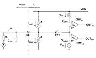
- FIG. 1 illustrates a circuit for error detection on a load according to the present invention.
- FIG. 2 illustrates a timing diagram for open load detection according to the present invention.
- FIG. 3 illustrates the battery voltage range of a detection circuit according to the present invention, with indication of error conditions.
- a device A coupled to a device B should not be limited to devices or systems wherein an output of device A is directly connected to an input of device B. It means that there exists a path between an output of A and an input of B which may be a path including other devices or means.
- a load in a normal or abnormal operation condition.
- load in the present patent application is not only meant the external load R L itself, but also the connection P to said external load R L . Not only the load R L can be defective; also the connection P to that load R L , the wire, can be broken or shorted to battery (power supply level) or ground. All these conditions should result in a defective load error message.
- the load is in an abnormal operation condition, then in a second phase, it is determined whether the load is in a short to battery, short to ground or open load condition. When an open load failure appears, this is detected in every measurement cycle.
- a circuit for detection of error conditions (short to battery, short to ground or open load —comprises two current sources I SRC and I SINK , as illustrated in FIG. 1 .
- the current sources can be part of a current digital-to-analog converter (DAC) used to drive the sensor in normal operation mode.
- DAC current digital-to-analog converter
- the circuit furthermore comprises comparing means, such as for example a first comparator CMP HI and a second comparator CMP LO .
- comparing means such as for example a first comparator CMP HI and a second comparator CMP LO .
- the positive input terminal of the first comparator CMPH HI and the negative input terminal of the second comparator CMP LO are connected together.
- the positive input terminal of the first comparator CMP HI and the negative input terminal of the second comparator CMP LO may be connected to a switching means SW 1 to a pin SP.
- Switching means SW 1 may be any kind of suitable switch, such as a mechanical switch or an electronic switch such as a transistor device for example.
- Switching means SW 1 is used for multiplexing the comparing means, e.g. the first and second comparators CMP HI and CMP LO , between different sensor pins. If no switching means is provided, then the comparing means, e.g. the first and second comparators CMP HI , CMP LO , are always connected to one and the same sensor pin and cannot be shared.
- the negative input terminal of the first comparator CMP HI is connected to a first voltage reference source V ref1 , which in turn is coupled to the supply power level VDD, so that the negative input terminal of the first comparator CMP HI , is at a potential level V refHI .
- the positive input terminal of the second comparator CMP LO is connected to a second voltage reference source V ref2 , which in turn is coupled to the ground, so that the positive input terminal of the second comparator is at a potential V refLO .
- an energy storing element is present, such as a capacitor C ext that is connected between the sensor pin SP and the ground or any other fixed potential, or such as an inductor (not represented in the drawings) that is coupled in series with the load, which makes the detection of open load condition more difficult.
- the error condition detection according to the present invention is done as follows.
- a first phase, diagnosis phase I as shown in FIG. 2 , during a normal operation measurement cycle, the first and second comparators CMP HI and CMP LO are connected through switching means SW 1 to the sensor pin. Output signals OUT HI , OUT LO of the first and second comparators CMP HI , CMP LO are strobed at strobe 1 . The first and second comparators CMP HI , CMP LO are monitoring whether the voltage on the pin SP goes below a certain level V refLO or above a certain level V refHI . If so, for example if any of the output signals OUT HI , OUT LO of the first and second comparators CMP HI , CMP LO is at one, the device reports a failure on the sensor pin SP.
- Table I gives an overview of possible conditions detected during diagnosis phase I.
- Phase I Phase I (Strobe 1) Phase I OUT HI OUT LO Diagnosis result 0 0 No error 1 0 Error condition (high voltage) 0 1 Error condition (low voltage)
- a second phase of diagnosis comprising two sub-phases IIa, IIb, needs to be activated. In normal mode, i.e. in case of non-error condition, this phase is disabled.
- the second phase is activated by a processor controlling the sequence, also called a master or a master controller, only when the master is sure that there is a real problem on the sensor pin, i.e. not in case of e.g. EMC distortion of a signal. If activated without real problem, this second phase could destroy the sensor.
- a processor controlling the sequence also called a master or a master controller
- the current flowing in or out the pin SP is changed to a pre-determined polarity and to a pre-determined level.
- Polarity of the current depends on the type of detected error, and the amplitude of the current is, when necessary, i.e. when it is smaller than a minimum current level, increased to be able to change the voltage on the pin SP, where the external capacitor C ext is connected, before a second strobe period (strobe 2 in FIG. 2 ).
- a minimum current is needed to change the voltage on the sensor pin SP in order to escape from the error condition. This minimum current is:
- I DiagMin ⁇ ⁇ ⁇ V ⁇ C ext t
- ⁇ V the voltage V ref
- Polarity of the current is changed in such a way that it is tried to “escape” from the error condition (see FIG. 3 ). If the voltage on the pin SP is below V refLO , which means that the load condition is either short to ground or open load, it is tried to source current from the device pin SP to increase the voltage on the pin above the V refLO voltage level. If this is possible, the load is in an open load condition. If, however, the voltage is stuck at ground (any voltage level below V refLO ), then the load is in a short circuit condition to ground. If the voltage on the pin SP is above V refHI , which means that the load condition is either short to the power supply or open load, it is tried to sink current into the device pin SP to decrease the voltage on the pin below the V refHI voltage. If this is possible, the load is in an open load condition. If, however, the voltage is stuck at the power supply level, or any voltage level above V refHI , then the load is in a short circuit condition to the power supply.
- Table II gives an overview of possible actions during diagnosis phase IIa.
- Phase I Strobe 1
- Phase IIa strobe 2
- Phase IIa OUT HI OUT LO OUT HI OUT LO
- Diagnosis result 0 0
- Nothing done Normal operation 1 0 1 0
- Short to power supply 1 0 0 X
- Open load 0 1 0 1
- Short to ground 0 1 X 0
- Open load 0
- the reset phase IIb takes at least the same time as phase IIa to be sure that the charge put in or out the capacitor C ext during the second diagnosis phase IIa is removed.
- the current is reinstated to its original amplitude level and polarity of the programmed current.
- the reason for the current reversing and keeping the amplitude level of the current during a certain time higher than the minimum level, as done during the reset phase IIb, is to be able to correctly detect the error in a next measurement cycle. If the current would not be at a high amplitude level during the reset phase IIb, then for small programmed currents in the next measurement cycle no error can be detected, because the voltage on the sensor pin SP will move too slowly due to the external capacitor C ext which is connected directly to the pin SP, as the charge put into this capacitor during the second diagnosis phase IIa is not removed then. The behaviour would be unacceptable.
Landscapes
- Testing Of Short-Circuits, Discontinuities, Leakage, Or Incorrect Line Connections (AREA)
- Emergency Protection Circuit Devices (AREA)
Abstract
Description
-
- during a first diagnosis phase, determining whether the load and/or the connection to the load are in a normal operation condition or in an error condition, and
- if the load and/or the connection to the load is in an error condition, during a second diagnosis phase determining whether the error condition is an open load condition, short circuit condition to ground or a short circuit condition to a power supply,
- wherein the second diagnosis phase comprises changing a first parameter associated with the load in an attempt to escape from the error condition.
ΔV being a reference voltage, Aext being a memory value of an energy storing element, for example a capacitance of an external capacitor, and t being the time between the change of the amplitude of the current and a moment of measuring a voltage on the pin.
-
- first diagnosis means for determining whether the load and/or the connection to the load are in a normal operation condition or in an error condition, and
- second diagnosis means for, if the load and/or the connection to the load is in an error condition, determining whether the error condition is an open load condition, short circuit condition to ground or a short circuit condition to power supply,
- and wherein the second diagnosis means comprises means for changing a first parameter associated with the load in an attempt to escape from the error condition.
ΔV being a reference voltage, Aext being a memory value of the energy storing element, for example capacitance of external capacitor Cext, and t being the time between the change of the amplitude of the current and a moment of measuring the voltage on the pin.
| TABLE I | ||||
| Phase I (Strobe 1) | Phase I | |||
| OUTHI | OUTLO | Diagnosis result | ||
| 0 | 0 | No |
||
| 1 | 0 | Error condition (high voltage) | ||
| 0 | 1 | Error condition (low voltage) | ||
where ΔV is the voltage Vref,
-
- ΔV is the voltage Vref,
- Cext is the capacitance of the external capacitor connected to the sensor pin SP,
- t is the time between the change (and increase) of the current and the second strobe.
| TABLE II | ||||
| Phase I (Strobe 1) | Current polarity | |||
| OUTHI | OUTLO | Phase IIa | ||
| 0 | 0 | No |
||
| 1 | 0 | |
||
| 0 | 1 | Source | ||
| TABLE III | ||
| Phase I (Strobe 1) | Phase IIa (strobe 2) | Phase IIa |
| OUTHI | OUTLO | OUTHI | OUTLO | Diagnosis result |
| 0 | 0 | Nothing done | |
| 1 | 0 | 1 | 0 | Short to |
|
| 1 | 0 | 0 | | Open load | |
| 0 | 1 | 0 | 1 | Short to ground | |
| 0 | 1 | |
0 | Open load | |
| TABLE IV | ||||
| Phase I (Strobe 1) | Current polarity | |||
| OUTHI | OUTLO | Phase IIb | ||
| 0 | 0 | No |
||
| 1 | 0 | |
||
| 0 | 1 | Sink | ||
Claims (19)
Applications Claiming Priority (2)
| Application Number | Priority Date | Filing Date | Title |
|---|---|---|---|
| EP03447077A EP1465313B1 (en) | 2003-04-02 | 2003-04-02 | Method and device for short circuit or open load detection |
| EPEP03447077.3 | 2003-04-02 |
Publications (2)
| Publication Number | Publication Date |
|---|---|
| US20040257735A1 US20040257735A1 (en) | 2004-12-23 |
| US7280333B2 true US7280333B2 (en) | 2007-10-09 |
Family
ID=32842918
Family Applications (1)
| Application Number | Title | Priority Date | Filing Date |
|---|---|---|---|
| US10/810,303 Active 2025-11-13 US7280333B2 (en) | 2003-04-02 | 2004-03-26 | Method and device for short circuit or open load detection |
Country Status (3)
| Country | Link |
|---|---|
| US (1) | US7280333B2 (en) |
| EP (1) | EP1465313B1 (en) |
| DE (1) | DE60332314D1 (en) |
Cited By (14)
| Publication number | Priority date | Publication date | Assignee | Title |
|---|---|---|---|---|
| US20090081979A1 (en) * | 2007-09-26 | 2009-03-26 | Infineon Technologies Ag | Radio-frequency front-end and receiver |
| US20090309607A1 (en) * | 2006-09-26 | 2009-12-17 | Continental Automotive Gmbh | Method and circuit arrangement for detecting the state of a load device which can be connected to a switching connection |
| US20100085178A1 (en) * | 2008-10-07 | 2010-04-08 | Katrak Kerfegar K | Discrete sensor inputs |
| US20100085082A1 (en) * | 2008-10-07 | 2010-04-08 | Katrak Kerfegar K | Ternary sensor inputs |
| US20100228455A1 (en) * | 2009-03-06 | 2010-09-09 | Katrak Kerfegar K | Transmission control module with valve control |
| US20100228431A1 (en) * | 2009-03-06 | 2010-09-09 | Katrak Kerfegar K | Transmission control module with multiple sensor inputs |
| US20110035123A1 (en) * | 2009-08-04 | 2011-02-10 | Katrak Kerfegar K | Shift rail transmission position sensing with tolerance for sensor loss |
| US20110031978A1 (en) * | 2008-04-10 | 2011-02-10 | Continental Automotive Gmbh | Apparatus and method for recognizing an error in a power bridge circuit |
| US20110169496A1 (en) * | 2010-01-14 | 2011-07-14 | SMR Patents S.a.r.I. | Fault detection of electric consumers in motor vehicles |
| US20120007603A1 (en) * | 2010-07-08 | 2012-01-12 | Wei Zhang | Circuits and methods for cell number detection |
| WO2013087604A1 (en) * | 2011-12-16 | 2013-06-20 | Continental Automotive Gmbh | Circuit arrangement for detecting a short circuit in a power switch |
| US10497296B2 (en) | 2017-09-21 | 2019-12-03 | Samsung Electronics Co., Ltd. | Operational amplifier circuit, data driving circuit, and operation methods of the same |
| US11506515B2 (en) * | 2017-08-15 | 2022-11-22 | Robert Bosch Gmbh | Control unit comprising a circuit, and method for short-circuit protection of ground lines and sensors |
| US11874340B2 (en) | 2022-05-31 | 2024-01-16 | Nxp Usa, Inc. | Open-circuit detector |
Families Citing this family (6)
| Publication number | Priority date | Publication date | Assignee | Title |
|---|---|---|---|---|
| EP1957992B1 (en) | 2005-12-06 | 2011-05-25 | Harman International Industries, Incorporated | Diagnostic system for power converter |
| US7804254B2 (en) * | 2006-04-19 | 2010-09-28 | Monolithic Power Systems, Inc. | Method and circuit for short-circuit and over-current protection in a discharge lamp system |
| US20070280313A1 (en) * | 2006-06-06 | 2007-12-06 | Chih-Cheng Hsieh | Method and Apparatus for Driving a Light Emitting Device |
| US7812590B2 (en) * | 2007-09-17 | 2010-10-12 | Infineon Technologies Ag | Method for detection of the presence of a load and drive circuit |
| US20140266106A1 (en) | 2013-03-14 | 2014-09-18 | Vidatronic, Inc. | Ldo and load switch supporting a wide range of load capacitance |
| DE102017201210A1 (en) | 2017-01-26 | 2018-07-26 | Robert Bosch Gmbh | Method and circuit arrangement for detecting a state of a load connected to a circuit connection |
Citations (6)
| Publication number | Priority date | Publication date | Assignee | Title |
|---|---|---|---|---|
| US4962350A (en) * | 1988-08-30 | 1990-10-09 | Alps Electric Co., Ltd. | Load condition detecting and driving system |
| US5294890A (en) * | 1991-06-07 | 1994-03-15 | Robert Bosch Gmbh | Examination circuit for a sensor |
| US5430438A (en) * | 1990-02-22 | 1995-07-04 | Robert Bosch Gmbh | Method and device for functional monitoring of an electrical load |
| US5886510A (en) * | 1996-09-17 | 1999-03-23 | MAGNETI MARELLI S.p.A. | Circuit for diagnosing the state of an electrical load |
| US6226602B1 (en) * | 1997-05-22 | 2001-05-01 | Robert Bosch Gmbh | Electric circuit arrangement |
| US20040004483A1 (en) * | 2002-07-02 | 2004-01-08 | Hazelton Lawrence Dean | Method and apparatus for control and fault detection of an electric load circuit |
Family Cites Families (3)
| Publication number | Priority date | Publication date | Assignee | Title |
|---|---|---|---|---|
| CH625932B (en) * | 1979-05-31 | Ebauches Electroniques Sa | INTEGRATED CIRCUIT SUITABLE TO REACT TO THE PRESENCE AND NATURE OF AN EXTERNAL RECEIVER CIRCUIT. | |
| EP0810444A1 (en) * | 1996-05-31 | 1997-12-03 | STMicroelectronics S.r.l. | Diagnosys circuit for possible faults during the driving phase of an electric load by a bridge stage |
| US5920452A (en) * | 1998-06-01 | 1999-07-06 | Harris Corporation | Circuit and method for protecting from overcurrent conditions and detecting an open electrical load |
-
2003
- 2003-04-02 EP EP03447077A patent/EP1465313B1/en not_active Expired - Lifetime
- 2003-04-02 DE DE60332314T patent/DE60332314D1/en not_active Expired - Lifetime
-
2004
- 2004-03-26 US US10/810,303 patent/US7280333B2/en active Active
Patent Citations (6)
| Publication number | Priority date | Publication date | Assignee | Title |
|---|---|---|---|---|
| US4962350A (en) * | 1988-08-30 | 1990-10-09 | Alps Electric Co., Ltd. | Load condition detecting and driving system |
| US5430438A (en) * | 1990-02-22 | 1995-07-04 | Robert Bosch Gmbh | Method and device for functional monitoring of an electrical load |
| US5294890A (en) * | 1991-06-07 | 1994-03-15 | Robert Bosch Gmbh | Examination circuit for a sensor |
| US5886510A (en) * | 1996-09-17 | 1999-03-23 | MAGNETI MARELLI S.p.A. | Circuit for diagnosing the state of an electrical load |
| US6226602B1 (en) * | 1997-05-22 | 2001-05-01 | Robert Bosch Gmbh | Electric circuit arrangement |
| US20040004483A1 (en) * | 2002-07-02 | 2004-01-08 | Hazelton Lawrence Dean | Method and apparatus for control and fault detection of an electric load circuit |
Cited By (30)
| Publication number | Priority date | Publication date | Assignee | Title |
|---|---|---|---|---|
| US20090309607A1 (en) * | 2006-09-26 | 2009-12-17 | Continental Automotive Gmbh | Method and circuit arrangement for detecting the state of a load device which can be connected to a switching connection |
| US8416546B2 (en) | 2006-09-26 | 2013-04-09 | Continental Automotive Gmbh | Method and circuit arrangement for detecting the state of a load device which can be connected to a switching connection |
| US10454511B2 (en) | 2007-09-26 | 2019-10-22 | Intel Mobile Communications GmbH | Radio-frequency front-end and receiver |
| US9755681B2 (en) * | 2007-09-26 | 2017-09-05 | Intel Mobile Communications GmbH | Radio-frequency front-end and receiver |
| US20090081979A1 (en) * | 2007-09-26 | 2009-03-26 | Infineon Technologies Ag | Radio-frequency front-end and receiver |
| US20110031978A1 (en) * | 2008-04-10 | 2011-02-10 | Continental Automotive Gmbh | Apparatus and method for recognizing an error in a power bridge circuit |
| US8860428B2 (en) * | 2008-04-10 | 2014-10-14 | Continental Automotive Gmbh | Apparatus and method for recognizing an error in a power bridge circuit |
| US20100085082A1 (en) * | 2008-10-07 | 2010-04-08 | Katrak Kerfegar K | Ternary sensor inputs |
| US20100085178A1 (en) * | 2008-10-07 | 2010-04-08 | Katrak Kerfegar K | Discrete sensor inputs |
| US8044787B2 (en) | 2008-10-07 | 2011-10-25 | Eaton Corporation | Discrete sensor inputs |
| US8204712B2 (en) | 2008-10-07 | 2012-06-19 | Eaton Corporation | Ternary sensor inputs |
| US20100228431A1 (en) * | 2009-03-06 | 2010-09-09 | Katrak Kerfegar K | Transmission control module with multiple sensor inputs |
| US20100228455A1 (en) * | 2009-03-06 | 2010-09-09 | Katrak Kerfegar K | Transmission control module with valve control |
| US10203033B2 (en) | 2009-03-06 | 2019-02-12 | Eaton Cummins Automated Transmission Technologies Llc | Transmission control module with multiple sensor inputs |
| US8510004B2 (en) | 2009-03-06 | 2013-08-13 | Eaton Corporation | Transmission control module with valve control |
| US20110035122A1 (en) * | 2009-08-04 | 2011-02-10 | Katrak Kerfegar K | Shift rail transmission position sensing with a minimum number of sensors |
| US20110035121A1 (en) * | 2009-08-04 | 2011-02-10 | Katrak Kerfegar K | Shift rail transmission position sensing |
| US20110035123A1 (en) * | 2009-08-04 | 2011-02-10 | Katrak Kerfegar K | Shift rail transmission position sensing with tolerance for sensor loss |
| US8606472B2 (en) | 2009-08-04 | 2013-12-10 | Eaton Corporation | Shift rail transmission position sensing with a minimum number of sensors |
| US8521376B2 (en) | 2009-08-04 | 2013-08-27 | Eaton Corporation | Shift rail transmission position sensing |
| US8521380B2 (en) | 2009-08-04 | 2013-08-27 | Eaton Corporation | Shift rail transmission position sensing with tolerance for sensor loss |
| EP2347932A1 (en) | 2010-01-14 | 2011-07-27 | SMR Patents S.à.r.l. | Malfunction recognition for electricity consumers in motor vehicles |
| US20110169496A1 (en) * | 2010-01-14 | 2011-07-14 | SMR Patents S.a.r.I. | Fault detection of electric consumers in motor vehicles |
| US8487633B2 (en) | 2010-01-14 | 2013-07-16 | Smr Patents S.A.R.L. | Fault detection of electric consumers in motor vehicles |
| US20120007603A1 (en) * | 2010-07-08 | 2012-01-12 | Wei Zhang | Circuits and methods for cell number detection |
| US8618806B2 (en) * | 2010-07-08 | 2013-12-31 | 02Micro, Inc. | Circuits and methods for cell number detection |
| WO2013087604A1 (en) * | 2011-12-16 | 2013-06-20 | Continental Automotive Gmbh | Circuit arrangement for detecting a short circuit in a power switch |
| US11506515B2 (en) * | 2017-08-15 | 2022-11-22 | Robert Bosch Gmbh | Control unit comprising a circuit, and method for short-circuit protection of ground lines and sensors |
| US10497296B2 (en) | 2017-09-21 | 2019-12-03 | Samsung Electronics Co., Ltd. | Operational amplifier circuit, data driving circuit, and operation methods of the same |
| US11874340B2 (en) | 2022-05-31 | 2024-01-16 | Nxp Usa, Inc. | Open-circuit detector |
Also Published As
| Publication number | Publication date |
|---|---|
| EP1465313B1 (en) | 2010-04-28 |
| EP1465313A1 (en) | 2004-10-06 |
| US20040257735A1 (en) | 2004-12-23 |
| DE60332314D1 (en) | 2010-06-10 |
Similar Documents
| Publication | Publication Date | Title |
|---|---|---|
| US7280333B2 (en) | Method and device for short circuit or open load detection | |
| KR100190479B1 (en) | Device for monitoring the function of an electric switch | |
| JP3185145B2 (en) | Fail safe state detection circuit | |
| US5731700A (en) | Quiescent power supply current test method and apparatus for integrated circuits | |
| KR100205838B1 (en) | Method and appratus for testing semiconductor integrated circuit | |
| JP5198062B2 (en) | System and method for detecting power failure conditions | |
| JP3139553B2 (en) | IC test equipment | |
| JPH05196677A (en) | Fault detecting device of driving circuit | |
| EP0163845B1 (en) | Diagnostic protection circuit and method | |
| KR102653766B1 (en) | Method and apparatus for automatically testing switching members | |
| JPWO2015053206A1 (en) | Electronic control unit | |
| US20090278066A1 (en) | Hydraulic valve control device and method for checking a hydraulic valve control device | |
| CN110958002B (en) | Solid state power switching device | |
| JPH10511470A (en) | Testable circuit and test method | |
| KR101955625B1 (en) | Apparatus and Method for Checking Fault of Relay | |
| US5077521A (en) | Supply connection integrity monitor | |
| US7265679B2 (en) | Apparatus and method for indicating onset of high-voltage at an output locus of a signal converter device | |
| JPH10257799A (en) | Output open-circuiting detection device of multichannel output device | |
| KR100895138B1 (en) | Delay circuit | |
| EP0566996A2 (en) | Programmable controller with erroneous input prevention control circuit | |
| JP4415384B2 (en) | DIGITAL OUTPUT DEVICE AND DIAGNOSIS METHOD USING DIGITAL OUTPUT DEVICE | |
| JP2019187050A (en) | Opening/ground fault detection circuit | |
| JPH05264658A (en) | Circuit having function for detecting end of life | |
| JP3196756B2 (en) | Semiconductor integrated circuit measuring device | |
| KR100367731B1 (en) | Internal electric power disconnection apparatus |
Legal Events
| Date | Code | Title | Description |
|---|---|---|---|
| AS | Assignment |
Owner name: AMI SEMICONDUCTOR BELGIUM BVBA, BELGIUM Free format text: ASSIGNMENT OF ASSIGNORS INTEREST;ASSIGNORS:HORSKY, PAVEL;KOUDAR, IVAN;REEL/FRAME:016362/0714;SIGNING DATES FROM 20040706 TO 20040709 |
|
| AS | Assignment |
Owner name: AMI SEMICONDUCTOR BELGIUM BVBA, BELGIUM Free format text: ASSIGNMENT OF ASSIGNORS INTEREST;ASSIGNORS:HORSKY, PAVEL;KOUDAR, IVAN;REEL/FRAME:016350/0132;SIGNING DATES FROM 20040706 TO 20040709 |
|
| STCF | Information on status: patent grant |
Free format text: PATENTED CASE |
|
| AS | Assignment |
Owner name: SEMICONDUCTOR COMPONENTS INDUSTRIES, L.L.C., ARIZO Free format text: BILL OF SALE;ASSIGNOR:AMI SEMICONDUCTOR BELGIUM BVBA;REEL/FRAME:023282/0476 Effective date: 20090228 Owner name: SEMICONDUCTOR COMPONENTS INDUSTRIES, L.L.C.,ARIZON Free format text: BILL OF SALE;ASSIGNOR:AMI SEMICONDUCTOR BELGIUM BVBA;REEL/FRAME:023282/0476 Effective date: 20090228 |
|
| FPAY | Fee payment |
Year of fee payment: 4 |
|
| FPAY | Fee payment |
Year of fee payment: 8 |
|
| AS | Assignment |
Owner name: DEUTSCHE BANK AG NEW YORK BRANCH, NEW YORK Free format text: SECURITY INTEREST;ASSIGNOR:SEMICONDUCTOR COMPONENTS INDUSTRIES, LLC;REEL/FRAME:038620/0087 Effective date: 20160415 |
|
| AS | Assignment |
Owner name: DEUTSCHE BANK AG NEW YORK BRANCH, AS COLLATERAL AG Free format text: CORRECTIVE ASSIGNMENT TO CORRECT THE INCORRECT PATENT NUMBER 5859768 AND TO RECITE COLLATERAL AGENT ROLE OF RECEIVING PARTY IN THE SECURITY INTEREST PREVIOUSLY RECORDED ON REEL 038620 FRAME 0087. ASSIGNOR(S) HEREBY CONFIRMS THE SECURITY INTEREST;ASSIGNOR:SEMICONDUCTOR COMPONENTS INDUSTRIES, LLC;REEL/FRAME:039853/0001 Effective date: 20160415 Owner name: DEUTSCHE BANK AG NEW YORK BRANCH, AS COLLATERAL AGENT, NEW YORK Free format text: CORRECTIVE ASSIGNMENT TO CORRECT THE INCORRECT PATENT NUMBER 5859768 AND TO RECITE COLLATERAL AGENT ROLE OF RECEIVING PARTY IN THE SECURITY INTEREST PREVIOUSLY RECORDED ON REEL 038620 FRAME 0087. ASSIGNOR(S) HEREBY CONFIRMS THE SECURITY INTEREST;ASSIGNOR:SEMICONDUCTOR COMPONENTS INDUSTRIES, LLC;REEL/FRAME:039853/0001 Effective date: 20160415 |
|
| MAFP | Maintenance fee payment |
Free format text: PAYMENT OF MAINTENANCE FEE, 12TH YEAR, LARGE ENTITY (ORIGINAL EVENT CODE: M1553); ENTITY STATUS OF PATENT OWNER: LARGE ENTITY Year of fee payment: 12 |
|
| AS | Assignment |
Owner name: FAIRCHILD SEMICONDUCTOR CORPORATION, ARIZONA Free format text: RELEASE OF SECURITY INTEREST IN PATENTS RECORDED AT REEL 038620, FRAME 0087;ASSIGNOR:DEUTSCHE BANK AG NEW YORK BRANCH, AS COLLATERAL AGENT;REEL/FRAME:064070/0001 Effective date: 20230622 Owner name: SEMICONDUCTOR COMPONENTS INDUSTRIES, LLC, ARIZONA Free format text: RELEASE OF SECURITY INTEREST IN PATENTS RECORDED AT REEL 038620, FRAME 0087;ASSIGNOR:DEUTSCHE BANK AG NEW YORK BRANCH, AS COLLATERAL AGENT;REEL/FRAME:064070/0001 Effective date: 20230622 |