US7253787B2 - Helix antenna and method for manufacturing the same - Google Patents

Helix antenna and method for manufacturing the same Download PDF

Info

Publication number
US7253787B2
US7253787B2 US11/099,616 US9961605A US7253787B2 US 7253787 B2 US7253787 B2 US 7253787B2 US 9961605 A US9961605 A US 9961605A US 7253787 B2 US7253787 B2 US 7253787B2
Authority
US
United States
Prior art keywords
circuit board
printed circuit
flexible printed
metal
annular surface
Prior art date
Legal status (The legal status is an assumption and is not a legal conclusion. Google has not performed a legal analysis and makes no representation as to the accuracy of the status listed.)
Expired - Fee Related, expires
Application number
US11/099,616
Other versions
US20060109196A1 (en
Inventor
Kuo-Cheng Liu
Chin-Hon Fan
Kun-Ting Lin
Ren-Peng Chen
Current Assignee (The listed assignees may be inaccurate. Google has not performed a legal analysis and makes no representation or warranty as to the accuracy of the list.)
HTC Corp
Original Assignee
High Tech Computer Corp
Priority date (The priority date is an assumption and is not a legal conclusion. Google has not performed a legal analysis and makes no representation as to the accuracy of the date listed.)
Filing date
Publication date
Priority claimed from TW93136269A external-priority patent/TWI248230B/en
Priority claimed from CNB200410102062XA external-priority patent/CN100574006C/en
Application filed by High Tech Computer Corp filed Critical High Tech Computer Corp
Assigned to HIGH TECH COMPUTER, CORP. reassignment HIGH TECH COMPUTER, CORP. ASSIGNMENT OF ASSIGNORS INTEREST (SEE DOCUMENT FOR DETAILS). Assignors: CHEN, REN-PENG, FAN, CHIN-HON, LIN, KUN-TING, LIU, KUO-CHENG
Publication of US20060109196A1 publication Critical patent/US20060109196A1/en
Priority to US11/826,763 priority Critical patent/US7411563B2/en
Application granted granted Critical
Publication of US7253787B2 publication Critical patent/US7253787B2/en
Expired - Fee Related legal-status Critical Current
Adjusted expiration legal-status Critical

Links

Images

Classifications

    • HELECTRICITY
    • H01ELECTRIC ELEMENTS
    • H01QANTENNAS, i.e. RADIO AERIALS
    • H01Q1/00Details of, or arrangements associated with, antennas
    • H01Q1/36Structural form of radiating elements, e.g. cone, spiral, umbrella; Particular materials used therewith
    • H01Q1/362Structural form of radiating elements, e.g. cone, spiral, umbrella; Particular materials used therewith for broadside radiating helical antennas
    • HELECTRICITY
    • H01ELECTRIC ELEMENTS
    • H01QANTENNAS, i.e. RADIO AERIALS
    • H01Q11/00Electrically-long antennas having dimensions more than twice the shortest operating wavelength and consisting of conductive active radiating elements
    • H01Q11/02Non-resonant antennas, e.g. travelling-wave antenna
    • H01Q11/08Helical antennas

Definitions

  • the invention relates to a method for manufacturing a helix antenna, and in particular to a method reducing manufacturing costs of a helix antenna.
  • Japan Patent. No. 2001-168631 discloses a conventional method for manufacturing a helix antenna providing a frequency of circularly polarized radiation exceeding 200 MHz.
  • a metal (copper) layer 2 is coated (electroplated) on the outer surface of a solid ceramic cylinder 1 in which a central through hole 3 is formed.
  • the metal (copper) layer 2 of the solid ceramic cylinder 1 is etched by a laser etching system (not shown), thereby providing a specific profile as shown in FIG. 1B .
  • a coaxial cable 4 with an exposed copper core 41 is disposed in the central through hole 3 of the solid ceramic cylinder 1 .
  • the copper core 41 is then bent and welded to the metal (copper) layer 2 on the top of the solid ceramic cylinder 1 , thereby achieving electrical connection between the coaxial cable 4 and the metal (copper) layer 2 .
  • the copper core 41 serves as a feeder.
  • the metal (copper) layer 2 cannot be precisely etched to form the specific profile by the laser etching system.
  • some parameters, such as radio frequency (RF) and impedance matching, of the helix antenna cannot be obtained as required.
  • a test and adjustment device (not shown) must then be applied to fine tune the parameters of the helix antenna.
  • the following description is directed to the steps of fine tuning the parameters of the helix antenna.
  • the method is simplified and can reduce manufacturing time and costs of the helix antenna.
  • the method can thus be applied to mass production of the helix antenna.
  • the method further comprises a step of passing the metal feeding strip through the central through hole from the first annular surface to the second annular surface of the ceramic cylinder.
  • the length of the flexible printed circuit board equals the circumference of the ceramic cylinder, and the width of the flexible printed circuit board equals the height of the ceramic cylinder.
  • the flexible printed circuit board provides a specific value of impedance matching.
  • a helix antenna comprising a ceramic cylinder and a flexible printed circuit board.
  • the ceramic cylinder comprises a central through hole, a first annular surface, and a second annular surface.
  • the first annular surface is opposite the second annular surface.
  • the central through hole is between the first and second annular surfaces.
  • the flexible printed circuit board is swirled and attached to the circumferential surface of the ceramic cylinder.
  • the flexible printed circuit board comprises a metal feeding strip extending outside the flexible printed circuit board and through the central through hole from the first annular surface to the second annular surface.
  • FIG. 1A is a schematic perspective view showing the manufacturing process of a conventional helix antenna
  • FIG. 1B is a schematic perspective view showing the manufacturing process of the conventional helix antenna of FIG. 1A ;
  • FIG. 1C is a schematic perspective view showing the manufacturing process of the conventional helix antenna of FIG. 1B ;
  • FIG. 1D is a schematic perspective view showing the manufacturing process of the conventional helix antenna of FIG. 1C ;
  • FIG. 2A is a schematic perspective view of the ceramic cylinder of the helix antenna of an embodiment of the invention.
  • FIG. 2B is a schematic plane view of the flexible printed circuit board of the helix antenna of an embodiment of the invention.
  • FIG. 3 is a schematic view showing assembly of the helix antenna of an embodiment of the invention.
  • the length L of the flexible printed circuit board 120 equals the circumference of the ceramic cylinder 110 , first annular surface 112 , or second annular surface 113 .
  • the width W of the flexible printed circuit board 120 equals the height of the ceramic cylinder 110 .
  • the flexible printed circuit board 120 comprises two first metal strips 131 , two second metal strips 132 , a metal feeding strip 133 , and a metal grounding strip 134 .
  • the first metal strips 131 are parallel to the second metal strips 132 .
  • the first metal strips 131 and second metal strips 132 tilt to one side of the flexible printed circuit board 120 at a predetermined angle ⁇ .
  • the metal feeding strip 133 is connected to the first metal strips 131 and extends outside the flexible printed circuit board 120 .
  • the metal grounding strip 134 is connected to the second metal strips 132 and extends outside the flexible printed circuit board 120 .
  • the flexible printed circuit board 120 is swirled and attached to the circumferential surface of the ceramic cylinder 110 .
  • the metal feeding strip 133 and metal grounding strip 134 are above the first annular surface 112 of the ceramic cylinder 110 .
  • the metal feeding strip 133 and metal grounding strip 134 pass through the central through hole 111 from the first annular surface 112 to the second annular surface 113 .
  • assembly of a helix antenna 100 is complete.
  • the first metal strips 131 and second metal strips 132 helically surround the ceramic cylinder 110 after the flexible printed circuit board 120 is swirled and attached to the circumferential surface of the ceramic cylinder 110 .

Landscapes

  • Details Of Aerials (AREA)

Abstract

A method for manufacturing a helix antenna. A ceramic cylinder including a central through hole, a first annular surface, and a second annular surface is provided. The first annular surface is opposite the second annular surface. The central through hole is between the first and second annular surfaces. A flexible printed circuit board with a metal feeding strip extending outside the flexible printed circuit board is provided. The flexible printed circuit board is swirled and attached to the circumferential surface of the ceramic cylinder.

Description

BACKGROUND
The invention relates to a method for manufacturing a helix antenna, and in particular to a method reducing manufacturing costs of a helix antenna.
Japan Patent. No. 2001-168631 discloses a conventional method for manufacturing a helix antenna providing a frequency of circularly polarized radiation exceeding 200 MHz. As shown in FIG. 1A, a metal (copper) layer 2 is coated (electroplated) on the outer surface of a solid ceramic cylinder 1 in which a central through hole 3 is formed. The metal (copper) layer 2 of the solid ceramic cylinder 1 is etched by a laser etching system (not shown), thereby providing a specific profile as shown in FIG. 1B. As shown in FIG. 1C, a coaxial cable 4 with an exposed copper core 41 is disposed in the central through hole 3 of the solid ceramic cylinder 1. The copper core 41 is then bent and welded to the metal (copper) layer 2 on the top of the solid ceramic cylinder 1, thereby achieving electrical connection between the coaxial cable 4 and the metal (copper) layer 2. At this point, the copper core 41 serves as a feeder. Accordingly, as the solid ceramic cylinder 1 is three-dimensional, the metal (copper) layer 2 cannot be precisely etched to form the specific profile by the laser etching system. Thus, some parameters, such as radio frequency (RF) and impedance matching, of the helix antenna cannot be obtained as required. A test and adjustment device (not shown) must then be applied to fine tune the parameters of the helix antenna.
The following description is directed to the steps of fine tuning the parameters of the helix antenna.
The helix antenna shown in FIG. 1C is connected to the test and adjustment device. Multiple probes of the test and adjustment device are coupled to the helix antenna, detecting magnitude of relative phases and amplitude of electric currents in some specific positions of the helix antenna. According to the detection of the probes, the laser etching system etches the metal (copper) layer 2 on the top of the solid ceramic cylinder 1, forming a plurality of openings 21, as shown in FIG. 1D. Specifically, to fine tune inductance of the helix antenna, the positions, profiles, and sizes of the openings 21 must be carefully arranged, thereby providing the helix antenna with a frequency of circularly polarized radiation exceeding 200 MHz.
A few drawbacks, however, exist in the process of manufacturing the aforementioned helix antenna. Bending and welding the copper core 41 to the metal (copper) layer 2 on the top of the solid ceramic cylinder 1 increases manufacturing time and causes inconvenience. Moreover, the laser etching system is very expensive and laser heads thereof must be replaced after 1500 hours, thereby increasing manufacturing costs of the helix antenna. Additionally, the duration for which the metal (copper) layer 2 is etched by the laser etching system is lengthy. Furthermore, as errors occur during etching of the metal (copper) layer 2 with the specific profile by the laser etching system, the helix antenna must be fine tuned by the test and adjustment device and laser etching system. Namely, the metal (copper) layer 2 on the top of the solid ceramic cylinder 1 is etched and the openings 21 are formed thereon. Accordingly, the process of fine tuning the helix antenna increases manufacturing time and costs thereof.
Hence, there is a need for an improved method for manufacturing a helix antenna. The method is simplified and can reduce manufacturing time and costs of the helix antenna. The method can thus be applied to mass production of the helix antenna.
SUMMARY
Accordingly, an exemplary embodiment of the invention provides a method for manufacturing a helix antenna. The method comprises the steps of providing a ceramic cylinder comprising a central through hole, a first annular surface, and a second annular surface, wherein the first annular surface is opposite the second annular surface, and the central through hole is between the first and second annular surfaces; providing a flexible printed circuit board comprising a metal feeding strip extending outside the flexible printed circuit board; and swirling and attaching the flexible printed circuit board to the circumferential surface of the ceramic cylinder.
In an embodiment of the method for manufacturing a helix antenna, the method further comprises a step of passing the metal feeding strip through the central through hole from the first annular surface to the second annular surface of the ceramic cylinder.
In an embodiment of the method for manufacturing a helix antenna, the flexible printed circuit board further comprises a metal grounding strip extending outside the flexible printed circuit board.
In an embodiment of the method for manufacturing a helix antenna, the method further comprises a step of passing the metal grounding strip through the central through hole from the first annular surface to the second annular surface of the ceramic cylinder.
In an embodiment of the method for manufacturing a helix antenna, the length of the flexible printed circuit board equals the circumference of the ceramic cylinder, and the width of the flexible printed circuit board equals the height of the ceramic cylinder.
In an embodiment of the method for manufacturing a helix antenna, the flexible printed circuit board further comprises at least one first metal strip and at least one second metal strip parallel thereto, the first and second metal strips tilt to one side of the flexible printed circuit board at a predetermined angle, the metal feeding strip is connected to the first metal strip, and the metal grounding strip is connected to the second metal strip.
In an embodiment of the method for manufacturing a helix antenna, the first and second metal strips are electroplated or printed on the flexible printed circuit board.
In an embodiment of the method for manufacturing a helix antenna, the flexible printed circuit board provides a specific value of impedance matching.
Another exemplary embodiment of the invention provides a helix antenna comprising a ceramic cylinder and a flexible printed circuit board. The ceramic cylinder comprises a central through hole, a first annular surface, and a second annular surface. The first annular surface is opposite the second annular surface. The central through hole is between the first and second annular surfaces. The flexible printed circuit board is swirled and attached to the circumferential surface of the ceramic cylinder. The flexible printed circuit board comprises a metal feeding strip extending outside the flexible printed circuit board and through the central through hole from the first annular surface to the second annular surface.
Further scope of the applicability of the present invention will become apparent from the detailed description given hereinafter. However, it should be understood that the detailed description and specific examples, while indicating preferred embodiments of the invention, are given by way of illustration only since various changes and modifications within the spirit and scope of the invention will become apparent to those skilled in the art from this detailed description.
DESCRIPTION OF THE DRAWINGS
The present invention will become more fully understood from the detailed description given hereinbelow and the accompanying drawings which arc given by way of illustration only, and thus are not limitative of the present invention, and wherein:
The invention can be more fully understood by reading the subsequent detailed description and examples with references made to the accompanying drawings, wherein:
FIG. 1A is a schematic perspective view showing the manufacturing process of a conventional helix antenna;
FIG. 1B is a schematic perspective view showing the manufacturing process of the conventional helix antenna of FIG. 1A;
FIG. 1C is a schematic perspective view showing the manufacturing process of the conventional helix antenna of FIG. 1B;
FIG. 1D is a schematic perspective view showing the manufacturing process of the conventional helix antenna of FIG. 1C;
FIG. 2A is a schematic perspective view of the ceramic cylinder of the helix antenna of an embodiment of the invention;
FIG. 2B is a schematic plane view of the flexible printed circuit board of the helix antenna of an embodiment of the invention;
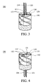
FIG. 3 is a schematic view showing assembly of the helix antenna of an embodiment of the invention; and
FIG. 4 is a schematic perspective view of the helix antenna of an embodiment of the invention.
DETAILED DESCRIPTION
Referring to FIG. 2A, a ceramic cylinder 110 is provided. The ceramic cylinder 110 comprises a central through hole 111, a first annular surface 112, and a second annular surface 113. The first annular surface 112 is opposite the second annular surface 113. The central through hole 111 is between the first annular surface 112 and the second annular surface 113.
Referring to FIG. 2B, a flexible printed circuit board (FPCB) 120, the parameters of which are finely tuned, is provided. Namely, some parameters, such as radio frequency (RF) and impedance matching, are finely tuned in the flexible printed circuit board 120. In this embodiment, the impedance matching of the flexible printed circuit board 120 is 50Ω when the receiving frequency is 1575.42 MHz.
As shown in FIG. 2B, the length L of the flexible printed circuit board 120 equals the circumference of the ceramic cylinder 110, first annular surface 112, or second annular surface 113. The width W of the flexible printed circuit board 120 equals the height of the ceramic cylinder 110.
The flexible printed circuit board 120 comprises two first metal strips 131, two second metal strips 132, a metal feeding strip 133, and a metal grounding strip 134. The first metal strips 131 are parallel to the second metal strips 132. Specifically, the first metal strips 131 and second metal strips 132 tilt to one side of the flexible printed circuit board 120 at a predetermined angle θ. The metal feeding strip 133 is connected to the first metal strips 131 and extends outside the flexible printed circuit board 120. The metal grounding strip 134 is connected to the second metal strips 132 and extends outside the flexible printed circuit board 120.
Referring to FIG. 3, the flexible printed circuit board 120 is swirled and attached to the circumferential surface of the ceramic cylinder 110. At this point, the metal feeding strip 133 and metal grounding strip 134 are above the first annular surface 112 of the ceramic cylinder 110. As shown in FIG. 2A and FIG. 4, the metal feeding strip 133 and metal grounding strip 134 pass through the central through hole 111 from the first annular surface 112 to the second annular surface 113. At this point, assembly of a helix antenna 100 is complete. Specifically, as tilting to one side of the flexible printed circuit board 120 at a predetermined angle θ, the first metal strips 131 and second metal strips 132 helically surround the ceramic cylinder 110 after the flexible printed circuit board 120 is swirled and attached to the circumferential surface of the ceramic cylinder 110.
Additionally, the first metal strips 131 and second metal strips 132 can be electroplated or printed on the flexible printed circuit board 120. Alternatively, the flexible printed circuit board 120 can be formed by electroplating or printing the first metal strips 131 and second metal strips 132 on a substrate.
In conclusion, the disclosed method for manufacturing the helix antenna 100 has the following advantages. The disclosed method does not require the process of bending and welding the copper core 41 to the metal (copper) layer 2 on the top of the solid ceramic cylinder 1, as shown in FIG. 1C and FIG. 1D, thus reducing manufacturing time and complexity. Moreover, the laser etching system and test and adjustment device are not required, such that manufacturing costs of the helix antenna 100 are reduced. Additionally, as important parameters in the flexible printed circuit board 120 are finely tuned before the flexible printed circuit board 120 is swirled and attached to the circumferential surface of the ceramic cylinder 110, fine-tuning operation of the parameters performed by the laser etching system and test and adjustment device is not required, further reducing the manufacturing costs and time of the helix antenna 100. Furthermore, as unity exists in the flexible printed circuit board(s) 120, mass production of the helix antenna 100 is available, thereby enhancing productivity.
While the invention has been described by way of example and in terms of preferred embodiment, it is to be understood that the invention is not limited thereto. To the contrary, it is intended to cover various modifications and similar arrangements (as would be apparent to those skilled in the art). Therefore, the scope of the appended claims should be accorded the broadest interpretation so as to encompass all such modifications and similar arrangements.

Claims (20)

1. A method for manufacturing a helix antenna, comprising:
providing a ceramic cylinder comprising a central through hole, a first annular surface, and a second annular surface, wherein the first annular surface is opposite the second annular surface, and the central through hole is between the first and second annular surfaces;
providing a flexible printed circuit board comprising a metal feeding strip extending outside the flexible printed circuit board;
swirling and attaching the flexible printed circuit board to the circumferential surface of the ceramic cylinder; and
passing the metal feeding strip through the central through hole from the first annular surface to the second annular surface of the ceramic cylinder.
2. The method as claimed in claim 1, wherein the flexible printed circuit board father comprises a metal grounding strip extending outside the flexible printed circuit board.
3. The method as claimed in claim 2, further comprising:
passing the metal grounding strip through the central through hole from the first annular surface to the second annular surface of the ceramic cylinder.
4. The method as claimed in claim 2, wherein the length of the flexible printed circuit board equals the circumference of the ceramic cylinder, and the width of the flexible printed circuit board equals the height of the ceramic cylinder.
5. The method as claimed in claim 4, wherein the flexible printed circuit board further comprises at least one first metal strip and at least one second metal strip parallel thereto, the first and second metal strips tilt to one side of the flexible printed circuit board at a predetermined angle, the metal feeding strip is connected to the first metal strip, and the metal grounding strip is connected to the second metal strip.
6. The method as claimed in claim 5, wherein the first and second metal strips are electroplated on the flexible printed circuit board.
7. The method as claimed in claim 5, wherein the first and second metal strips are printed on the flexible printed circuit board.
8. The method as claimed in claim 1, wherein the flexible printed circuit board provides a specific value of impedance matching.
9. The method as claimed in claim 1, wherein the length of the flexible printed circuit board equals the circumference of the ceramic cylinder, and the width of the flexible printed circuit board equals the height of the ceramic cylinder.
10. The method as claimed in claim 2, wherein the flexible printed circuit board further comprises at least one first metal strip and at least one second metal strip parallel thereto, the first and second metal strips tilt to one side of the flexible printed circuit board at a predetermined angle, the metal feeding strip is connected to the first metal strip, and the metal grounding suip is connected to the second metal strip.
11. A helix antenna, comprising:
a ceramic cylinder comprising a central through hole, a first annular surface, and a second annular surface, wherein the first annular surface is opposite the second annular surface, and the central through hole is between the first and second annular surfaces; and
a flexible printed circuit board swirled and attached to the circumferential surface of the ceramic cylinder, wherein the flexible printed circuit board comprises a metal feeding strip extending outside the flexible printed circuit board and through the central through hole from the first annular surface to the second annular surface.
12. The helix antenna as claimed in claim 11, wherein the flexible printed circuit board further comprises a metal grounding strip extending outside the flexible printed circuit board and through the central through hole from the first annular surface to the second annular surface.
13. The helix antenna as claimed in claim 12, wherein the length of the flexible printed circuit board equals the circumference of the ceramic cylinder, and the width of the flexible printed circuit board equals the height of the ceramic cylinder.
14. The helix antenna as claimed in claim 13, wherein the flexible printed circuit board further comprises at least one first metal strip and at least one second metal strip parallel thereto, the first and second metal strips tilt to one side of the flexible printed circuit board at a predetermined angle, the metal feeding strip is connected to the first metal strip, and the metal grounding strip is connected to the second metal strip.
15. The helix antenna as claimed in claim 14, wherein the first and second metal strips are electroplated on the flexible printed circuit board.
16. The helix antenna as claimed in claim 14, wherein the first and second metal strips are printed on the flexible printed circuit board.
17. The helix antenna as claimed in claim 11, wherein the flexible printed circuit board provides a specific value of impedance matching.
18. The helix antenna as claimed in claim 11, wherein the length of the flexible printed circuit board equals the circumference of the ceramic cylinder, and the width of the flexible printed circuit board equals the height of the ceramic cylinder.
19. The helix antenna as claimed in claim 12, wherein the flexible printed circuit board further comprises at least one first metal strip and at least one second metal strip parallel thereto, the first and second metal strips tilt to one side of the flexible printed circuit board at a predetermined angle, the metal feeding strip is connected to the first metal strip, and the metal grounding strip is connected to the second metal strip.
20. A helix antenna, comprising:
a ceramic cylinder comprising a central through hole, a first annular surface, and a second annular surface, wherein the first annular surface is opposite the second annular surface, and the central through hole is between the first and second annular surfaces; and
a flexible printed circuit board swirled and attached to the circumferential surface of the ceramic cylinder, wherein the flexible printed circuit board comprises a metal feeding strip and a metal grounding strip, and the metal feeding strip and metal grounding strip extend outside the flexible printed circuit board and through the central through hole from the first annular surface to the second annular surface, respectively.
US11/099,616 2004-11-25 2005-04-06 Helix antenna and method for manufacturing the same Expired - Fee Related US7253787B2 (en)

Priority Applications (1)

Application Number Priority Date Filing Date Title
US11/826,763 US7411563B2 (en) 2004-11-25 2007-07-18 Antenna device

Applications Claiming Priority (4)

Application Number Priority Date Filing Date Title
TW93136269A TWI248230B (en) 2004-11-25 2004-11-25 Method for manufacturing a helix antenna
TW93136269 2004-11-25
CNB200410102062XA CN100574006C (en) 2004-12-17 2004-12-17 The manufacture method of helical antenna and helical antenna
CN200410102062.X 2004-12-17

Related Child Applications (1)

Application Number Title Priority Date Filing Date
US11/826,763 Continuation US7411563B2 (en) 2004-11-25 2007-07-18 Antenna device

Publications (2)

Publication Number Publication Date
US20060109196A1 US20060109196A1 (en) 2006-05-25
US7253787B2 true US7253787B2 (en) 2007-08-07

Family

ID=36460469

Family Applications (2)

Application Number Title Priority Date Filing Date
US11/099,616 Expired - Fee Related US7253787B2 (en) 2004-11-25 2005-04-06 Helix antenna and method for manufacturing the same
US11/826,763 Expired - Fee Related US7411563B2 (en) 2004-11-25 2007-07-18 Antenna device

Family Applications After (1)

Application Number Title Priority Date Filing Date
US11/826,763 Expired - Fee Related US7411563B2 (en) 2004-11-25 2007-07-18 Antenna device

Country Status (1)

Country Link
US (2) US7253787B2 (en)

Cited By (7)

* Cited by examiner, † Cited by third party
Publication number Priority date Publication date Assignee Title
US20060082517A1 (en) * 2004-09-30 2006-04-20 Shyh-Jong Chung Antenna
US20070262915A1 (en) * 2004-11-25 2007-11-15 Kuo-Cheng Liu Antenna device
US20110047789A1 (en) * 2009-08-26 2011-03-03 Lyders David R Electrical probe assembly
US8106846B2 (en) 2009-05-01 2012-01-31 Applied Wireless Identifications Group, Inc. Compact circular polarized antenna
US8618998B2 (en) 2009-07-21 2013-12-31 Applied Wireless Identifications Group, Inc. Compact circular polarized antenna with cavity for additional devices
US11349218B2 (en) * 2019-06-13 2022-05-31 KYOCERA AVX Components (San Diego), Inc. Antenna assembly having a helical antenna disposed on a flexible substrate wrapped around a tube structure
US11682841B2 (en) 2021-09-16 2023-06-20 Eagle Technology, Llc Communications device with helically wound conductive strip and related antenna devices and methods

Families Citing this family (4)

* Cited by examiner, † Cited by third party
Publication number Priority date Publication date Assignee Title
US20070063918A1 (en) * 2005-06-21 2007-03-22 Leisten Oliver P Antenna and an antenna feed structure
KR100821981B1 (en) * 2007-02-02 2008-04-15 이성철 Dielectrics omnidirection antenna
CN105552546A (en) * 2016-01-29 2016-05-04 惠州硕贝德无线科技股份有限公司 Small-sized big dipper antenna
CN108422074B (en) * 2018-05-11 2023-11-10 天津航天机电设备研究所 Spiral weld electron beam welding fixture and heat dissipation tool

Citations (9)

* Cited by examiner, † Cited by third party
Publication number Priority date Publication date Assignee Title
JPH04220165A (en) 1990-02-06 1992-08-11 Nec Corp Soldering method by laser beam
JPH06212477A (en) 1993-01-12 1994-08-02 Ricoh Co Ltd Production of fine structure
EP0791978A2 (en) 1996-02-23 1997-08-27 Symmetricom, Inc. An antenna
WO1998044590A1 (en) 1997-03-27 1998-10-08 Qualcomm Incorporated An antenna and a feed network for an antenna
US5828348A (en) * 1995-09-22 1998-10-27 Qualcomm Incorporated Dual-band octafilar helix antenna
US6184845B1 (en) * 1996-11-27 2001-02-06 Symmetricom, Inc. Dielectric-loaded antenna
US6184844B1 (en) * 1997-03-27 2001-02-06 Qualcomm Incorporated Dual-band helical antenna
JP2001168631A (en) 1999-11-05 2001-06-22 Sarantel Ltd Manufacture of antenna
US20020140622A1 (en) 2001-03-29 2002-10-03 Samsung Electro-Mechanics Co. Ltd. Antenna, and manufacturing method therefor

Family Cites Families (6)

* Cited by examiner, † Cited by third party
Publication number Priority date Publication date Assignee Title
JPH0623055Y2 (en) 1988-02-29 1994-06-15 日本無線株式会社 Helical antenna
JP2719856B2 (en) 1991-07-05 1998-02-25 シャープ株式会社 Backfire helical antenna
JPH0677722A (en) 1992-08-19 1994-03-18 Mitsubishi Electric Corp Antenna device
JP2701747B2 (en) 1994-09-06 1998-01-21 日本電気株式会社 Helical antenna
SE511450C2 (en) * 1997-12-30 1999-10-04 Allgon Ab Antenna system for circularly polarized radio waves including antenna device and interface network
US7253787B2 (en) * 2004-11-25 2007-08-07 High Tech Computer, Corp. Helix antenna and method for manufacturing the same

Patent Citations (9)

* Cited by examiner, † Cited by third party
Publication number Priority date Publication date Assignee Title
JPH04220165A (en) 1990-02-06 1992-08-11 Nec Corp Soldering method by laser beam
JPH06212477A (en) 1993-01-12 1994-08-02 Ricoh Co Ltd Production of fine structure
US5828348A (en) * 1995-09-22 1998-10-27 Qualcomm Incorporated Dual-band octafilar helix antenna
EP0791978A2 (en) 1996-02-23 1997-08-27 Symmetricom, Inc. An antenna
US6184845B1 (en) * 1996-11-27 2001-02-06 Symmetricom, Inc. Dielectric-loaded antenna
WO1998044590A1 (en) 1997-03-27 1998-10-08 Qualcomm Incorporated An antenna and a feed network for an antenna
US6184844B1 (en) * 1997-03-27 2001-02-06 Qualcomm Incorporated Dual-band helical antenna
JP2001168631A (en) 1999-11-05 2001-06-22 Sarantel Ltd Manufacture of antenna
US20020140622A1 (en) 2001-03-29 2002-10-03 Samsung Electro-Mechanics Co. Ltd. Antenna, and manufacturing method therefor

Cited By (9)

* Cited by examiner, † Cited by third party
Publication number Priority date Publication date Assignee Title
US20060082517A1 (en) * 2004-09-30 2006-04-20 Shyh-Jong Chung Antenna
US20070262915A1 (en) * 2004-11-25 2007-11-15 Kuo-Cheng Liu Antenna device
US7411563B2 (en) * 2004-11-25 2008-08-12 High Tech Computer, Corp. Antenna device
US8106846B2 (en) 2009-05-01 2012-01-31 Applied Wireless Identifications Group, Inc. Compact circular polarized antenna
US8618998B2 (en) 2009-07-21 2013-12-31 Applied Wireless Identifications Group, Inc. Compact circular polarized antenna with cavity for additional devices
US20110047789A1 (en) * 2009-08-26 2011-03-03 Lyders David R Electrical probe assembly
US8816711B2 (en) * 2009-08-26 2014-08-26 United Technologies Corporation Electrical probe assembly
US11349218B2 (en) * 2019-06-13 2022-05-31 KYOCERA AVX Components (San Diego), Inc. Antenna assembly having a helical antenna disposed on a flexible substrate wrapped around a tube structure
US11682841B2 (en) 2021-09-16 2023-06-20 Eagle Technology, Llc Communications device with helically wound conductive strip and related antenna devices and methods

Also Published As

Publication number Publication date
US7411563B2 (en) 2008-08-12
US20060109196A1 (en) 2006-05-25
US20070262915A1 (en) 2007-11-15

Similar Documents

Publication Publication Date Title
US7253787B2 (en) Helix antenna and method for manufacturing the same
US7075486B2 (en) Circularly polarized wave antenna made of sheet metal with high reliability
US7248224B2 (en) Antenna device having radiation characteristics suitable for ultrawideband communications
US6339402B1 (en) Low profile tunable circularly polarized antenna
US6677909B2 (en) Dual band slot antenna with single feed line
US6339405B1 (en) Dual band dipole antenna structure
US6778149B2 (en) Composite antenna apparatus
JP2005176294A (en) Antenna assembly
EP1672737A1 (en) Helix antenna and method for manufacturing the same
US20080122731A1 (en) Method for mounting a tridimensional antenna
US20060176237A1 (en) Small broadband helical antenna
US20100149049A1 (en) Broadband antenna of dual resonance
WO2010077574A2 (en) Multiband high gain omnidirectional antennas
JP4176761B2 (en) Helical antenna and manufacturing method thereof
US7030816B2 (en) Printed PIFA antenna and method of making the same
US6483465B2 (en) Circularly polarized wave antenna and manufacturing method therefor
JP4798356B2 (en) Patch antenna and manufacturing method thereof
US6727858B2 (en) Circularly polarized wave antenna suitable for miniaturization
US11211712B1 (en) Compact integrated GNSS-UHF antenna system
US20050206578A1 (en) Dual band antenna
JP2009296270A (en) Antenna device
US20050151694A1 (en) Notched slot antenna
JP3743324B2 (en) Antenna module and portable device using the same
US20030184483A1 (en) Dielectric chip antenna
JPH06303163A (en) Portable radio equipment

Legal Events

Date Code Title Description
AS Assignment

Owner name: HIGH TECH COMPUTER, CORP., TAIWAN

Free format text: ASSIGNMENT OF ASSIGNORS INTEREST;ASSIGNORS:LIU, KUO-CHENG;FAN, CHIN-HON;LIN, KUN-TING;AND OTHERS;REEL/FRAME:016452/0899

Effective date: 20050223

STCF Information on status: patent grant

Free format text: PATENTED CASE

FPAY Fee payment

Year of fee payment: 4

FPAY Fee payment

Year of fee payment: 8

FEPP Fee payment procedure

Free format text: MAINTENANCE FEE REMINDER MAILED (ORIGINAL EVENT CODE: REM.); ENTITY STATUS OF PATENT OWNER: LARGE ENTITY

LAPS Lapse for failure to pay maintenance fees

Free format text: PATENT EXPIRED FOR FAILURE TO PAY MAINTENANCE FEES (ORIGINAL EVENT CODE: EXP.); ENTITY STATUS OF PATENT OWNER: LARGE ENTITY

STCH Information on status: patent discontinuation

Free format text: PATENT EXPIRED DUE TO NONPAYMENT OF MAINTENANCE FEES UNDER 37 CFR 1.362

FP Lapsed due to failure to pay maintenance fee

Effective date: 20190807