US6558564B1 - Plasma energy control by inducing plasma instability - Google Patents
Plasma energy control by inducing plasma instability Download PDFInfo
- Publication number
- US6558564B1 US6558564B1 US09/543,392 US54339200A US6558564B1 US 6558564 B1 US6558564 B1 US 6558564B1 US 54339200 A US54339200 A US 54339200A US 6558564 B1 US6558564 B1 US 6558564B1
- Authority
- US
- United States
- Prior art keywords
- plasma
- electron temperature
- electron
- power
- reactor
- Prior art date
- Legal status (The legal status is an assumption and is not a legal conclusion. Google has not performed a legal analysis and makes no representation as to the accuracy of the status listed.)
- Expired - Fee Related
Links
Images


Classifications
-
- H—ELECTRICITY
- H01—ELECTRIC ELEMENTS
- H01J—ELECTRIC DISCHARGE TUBES OR DISCHARGE LAMPS
- H01J37/00—Discharge tubes with provision for introducing objects or material to be exposed to the discharge, e.g. for the purpose of examination or processing thereof
- H01J37/32—Gas-filled discharge tubes
- H01J37/32009—Arrangements for generation of plasma specially adapted for examination or treatment of objects, e.g. plasma sources
- H01J37/32082—Radio frequency generated discharge
Definitions
- One problem encountered in high-density plasma reactors used to process semiconductor wafers in the production of integrated circuits is electrical charge damage to certain integrated circuit features on the wafer.
- Charge damage is caused by the difference in velocity distributions of electrons and ions near the wafer surface in surface features having relatively high aspect ratios.
- the velocity distribution of the plasma ions is vertical, due to the vertical electric field lines near the surface of the wafer induced by an RF bias signal applied to the wafer.
- the velocity distribution of the plasma electrons approaches an isotropic distribution despite the vertical electric field lines near the wafer surface because of the high electron temperature characteristic of a high density plasma reactor.
- the vertical trajectory of the ions enables them to travel completely down the entire depth of the opening, so that they nearly all strike the bottom of the opening.
- the nearly isotropic velocity distribution of the electrons enables them to strike the sidewall of the opening, so that only a relatively small portion of the electrons are able to strike the bottom of the opening.
- the bottom of the opening acquires a positive charge while the top of the opening acquires a negative charge.
- this effect is exacerbated and the resulting internal electric fields within the microelectronic features on the wafer can damage those features, resulting in device failure.
- RF plasma source power modulation is a well-known technique for modifying average plasma electron temperature and plasma chemistry, by pulsing (time-modulating) the RF plasma source power signal.
- This technique provides some control of electron temperature independent of the RF plasma source power level. This is because the electron temperature decreases at a much quicker rate than plasma density during the power off time between pulses. This control is gained by choosing an appropriate pulse width and pulse repetition rate of the pulse-modulated plasma RF power source so as to reduce the electron temperature without having to reduce the power level.
- Pulse-modulating the RF plasma source power has the advantage of not requiring a drastic change in power level to reduce electron temperature.
- this technique does require the RF plasma source power to be modified by pulse modulation. It is a goal of the present invention to reduce plasma electron temperature without having to modify the plasma source power generator (e.g., by the introduction of pulse modulation).
- electron temperature is controlled by inducing or enhancing natural instability waves in the plasma.
- FIG. 1 is a schematic diagram of a plasma reactor system embodying the invention.
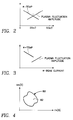
- FIG. 2 is a graph illustrating the effects of chamber pressure in an electro-negative plasma on electron temperature and on plasma fluctuation amplitude.
- FIG. 3 is a graph illustrating the effects of e-beam current on electron temperature and on plasma fluctuation amplitude.
- FIG. 4 is a graph illustrating the impedance match space of the impedance match network of the system of FIG. 1 .
- FIG. 5 is a graph illustrating the effects of changing a parameter of the impedance match system on electron temperature and on plasma fluctuation amplitude.
- FIG. 6 is a block diagram illustrating a method of the invention including the generation and use of a look-up table correlating electron temperature and a selected control parameter of the system.
- FIG. 7 illustrates a look-up table employed in carrying out the method of FIG. 6 .
- FIG. 8 illustrates one method of controlling the frequency of the impedance match system to achieve desired plasma fluctuations.
- electron temperature is controlled by inducing or enhancing natural instability waves in the plasma. This can be accomplished by introducing instabilities between the plasma and the power source. As a result, no pulse modulation of the RF power or RF generator is required, a significant advantage. The instability is enhanced until the desired reduction in electron temperature has been achieved. In accordance with the invention, there are several modes for inducing such a natural instability.
- the rate of electron attachment is enhanced by increasing the reactor chamber pressure.
- the loss of electrons can lead to an instability between the plasma and the feedback control system regulating the RF plasma source power generator, causing fluctuations in the delivered RF power.
- the chamber pressure preferably is increased so as to increase such RF power fluctuations until a desired decrease in plasma electron temperature has been achieved.
- the rate of ion recombination is enhanced by introducing an electron beam into the plasma from an e-beam generator.
- Introduction of the additional electrons by the e-beam generator increases the rate of ion-to-electron recombination and can also lead to beam-plasma interaction instabilities.
- the resulting loss in ion density leads to an instability between the plasma and the feedback control system regulating the RF plasma source power generator, causing fluctuations in the delivered RF power.
- the electron beam current preferably is increased so as to increase such RF power fluctuations until a desired decrease in plasma electron temperature has been achieved.
- natural plasma instabilities are enhanced by introducing an instability between the load impedance presented by the plasma and the impedance match feedback control system of the RF plasma source power generator. This is accomplished by changing a selected parameter of the impedance match network in such a way as to change the impedance match space relative to the load impedance presented to the RF generator until the impedance match feedback control network enters an unstable regime in which it fluctuates or oscillates.
- the impedance match network typically includes an element having a variable reactance which the impedance match feedback control system varies to minimize the amount of power reflected back to the RF generator.
- the fluctuations of the impedance match feedback control system are manifested as fluctuations in the reactance of the variable reactance element or in delivered power in systems where forward power is servoed. These fluctuations can couple with natural plasma instabilities such as drift waves and ion acoustic waves, causing fluctuations in the power delivered to the plasma.
- the selected parameter of the impedance match network is modified until these fluctuations reach a level at which the electron temperature has been decreased by a desired amount.
- the selected parameter of the impedance match network may be the reactance of an otherwise fixed element (e.g., a capacitor or inductor) within the impedance match network, the frequency of the RF power generator or the Q of the impedance match feedback control system.
- the frequency of the RF power generator is changed by, for example, changing the control voltage applied to a voltage controlled oscillator (VFO) of the generator.
- VFO voltage controlled oscillator
- the Q of the control system may be changed by, for example, changing the value of a resistor or an RC time constant within the impedance match feedback control system.
- the foregoing methods of the invention are carried out by observing electron temperature using a conventional electron temperature probe such as a Langmuir probe placed inside the reactor chamber.
- a computer may be employed to record measured electron temperature across a range of values of the selected parameter (e.g., where the selected parameter is one of the following: chamber pressure, e-beam current, impedance match network element reactance, RF frequency or match Q).
- the selected parameter is one of the following: chamber pressure, e-beam current, impedance match network element reactance, RF frequency or match Q.
- a look-up table is constructed for use in a production plasma reactor having no electron-temperature sensitive probe. The look-up table determines which parameter value is appropriate for a desired electron temperature level.
- the desired electron temperature level can be determined by trial and error by processing a number of wafers with identical microelectronic features at different electron temperature levels and measuring the amount of charge damage on each wafer.
- the wafers may be processed sequentially in the same reactor at progressively decreasing levels of electron temperature until a wafer is processed in which the measured amount of charge damage reaches an acceptable level or disappears altogether, the electron temperature environment of this wafer being the desired electron temperature.
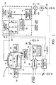
- a plasma reactor 10 has a cylindrical side wall 12 and a ceiling 14 which may be dome-shaped, the wall 12 and ceiling 14 defining a vacuum chamber 16 into which process gases are introduced through a gas inlet 18 from a gas supply 20 .
- a workpiece support 22 supports a semiconductor wafer 24 .
- Gas pressure within the chamber 16 is controlled by a pressure control system 26 which includes a vacuum pump and a pressure sensor (not shown). Chamber pressure is commanded by an applied voltage controlled, in a simplified example, by a variable resistor 28 .
- RF plasma source power i.e., that power required to ionize the process gases in the chamber to generate a plasma
- RF power generator 30 i.e., that power required to ionize the process gases in the chamber to generate a plasma
- the reactor 10 provides a high density plasma by inductively coupling the source power into the chamber 16 .
- the RF power is applied to an inductive antenna 34 overlying the ceiling 14 .
- the impedance match system 32 is of the conventional type which includes a bridge circuit 70 connected in series between the output of the RF generator 30 and the impedance match network 50 , the bridge circuit 70 being of the conventional type which separates forward voltage from reflected voltage.
- the impedance match network 50 includes passive reactive elements, capacitors and inductors, defining the match space of the impedance match system 32 . At least one of the reactive elements is variable, such as the variable capacitor 74 .
- the impedance of the variable capacitor 74 is controlled in a feedback loop consisting of a conventional impedance match controller 78 .
- the controller's output is connected to vary the variable capacitor 74 and the controller's error input is connected to the reflected voltage output of the bridge circuit 70 .
- the controller 78 thus varies the capacitor 74 in such a manner as to minimize the reflected voltage at the generator 30 .
- the output impedance presented by the generator 30 and impedance match network 50 equals the load impedance presented by the chamber and plasma.
- the reactor may further include a conventional delivered power controller 79 .
- the delivered power controller 79 typically is programmed to maintain forward power, as sensed on the double balanced bridge 70 , at a particular level.
- the delivered power controller 79 has a control output coupled to a power level control input 30 a of the RF generator 30 .
- the delivered power controller 79 reduces the control voltage at the generator's control input 30 a whenever the forward power sensed at the bridge 70 exceeds the desired level and increases it whenever the forward power falls below the desired level.
- the gas supply 20 furnishes electro-negative gases into the chamber 16 , such as SF 6 for a tungsten etch process or C 12 for a metal or polysilicon etch process, for example. Generally, such process are carried out at a chamber pressure below 30-50 mT. In accordance with the present invention, the chamber pressure is increased into the range of 30-50 mT to promote electron attachment in the electro-negative plasma. This changes the load impedance of the plasma presented to the generator 30 , which the impedance match system 32 overcorrects, creating an instability in the plasma, manifested as fluctuations in the delivered power from the generator 30 .
- the chamber pressure is increased in this manner until the fluctuations in delivered RF power cause the plasma electron temperature to decrease to a desired level, such as a level at which charge damage to microelectronic features on the wafer 24 does not occur.
- the electron temperature is measured in an experimental version of the reactor 10 which is specially modified to include an electron-temperature-sensitive probe 40 , such as a Langmuir probe, for example.
- the output of the probe is fed to a computer 42 .
- the computer 42 may be programmed to correlate electron temperature measurements from the probe with instantaneous chamber pressure values from the pressure controller 26 .
- the computer 42 can form a look-up table 44 correlating chamber pressure and electron temperature.
- there is no probe 40 there is no probe 40 , and the desired electron temperature is reached by referring in the look-up table 44 to the chamber pressure corresponding to the desired electron temperature.
- FIG. 2 illustrates in a qualitative manner the approximate behavior of the electron temperature with the chamber pressure: As chamber pressure increases, the electron temperature decreases. FIG. 2 also illustrates the amplitude of fluctuations in the delivered RF power to the plasma as a function of chamber pressure: As the chamber pressure is increased, the rate of electron attachment to neutral species, to form anions, increases. In an inductively coupled plasma, electrons and not ions are accelerated by the applied RF field, and are necessary to impart kinetic energy to the process gas for ionization. Thus, electron attachment decreases electron density, thereby changing the load impedance presented to the generator 30 . In response, the impedance match system 32 overcompensates by changing the impedance of a match network 50 .
- the system includes a forward power servo control system of the conventional type such as the delivered power controller 79 of FIG. 1, then such changes may cause the controller 79 to overcorrect the delivered (forward) power.
- the resulting overcorrection in plasma ion density causes the match system 32 to overcorrect in the opposite direction, leading to oscillations. These oscillations cause oscillations in the power coupled to the plasma, so that the average electron temperature falls, as illustrated in FIG. 2 .
- an electro-positive gas is supplied by the gas supply 20 into the chamber 16 .
- Natural instabilities between the plasma and the generator 30 are induced by introducing an electron beam from an e-beam generator 60 into the chamber 16 .
- the additional electrons thus introduced increase the rate at which plasma ions are lost to recombination with electrons, or can introduce a plasma-electron beam interaction instability.
- the loss of plasma ion density causes a change in the plasma load impedance presented to the generator 30 .
- the impedance match system 32 overcompensates by changing the impedance of a match network 50 .
- the system includes a forward power servo control system of the conventional type such as the delivered power controller 79 of FIG.
- the controller 79 may overcorrect the delivered (forward) power.
- the resulting overcorrection in plasma ion density causes the match system 32 to overcorrect in the opposite direction, leading to oscillations.
- These oscillations cause oscillations in the power coupled to the plasma which increase as the electron beam current is increased, so that the average electron temperature falls with increasing e-beam current, as illustrated in FIG. 3 .
- the e-beam current is controlled, in a simple example, by a variable resistor 62 connected to a control input of the e-beam generator 60 .
- the e-beam current is increased until the requisite decrease in plasma electron temperature is achieved.
- the computer 42 receives the e-beam current setting at the input to the e-beam generator 60 , so that the computer 42 can form the look-up table 44 to correlate e-beam current with plasma electron temperature.
- FIG. 3 illustrates in a qualitative manner the approximate behavior of the electron temperature with the e-beam current: As the e-beam current increases, the electron temperature decreases.
- FIG. 2 also illustrates the amplitude of fluctuations in the delivered RF power to the plasma as a function of the e-beam current: As the e-beam current is increased, the rate of ion-to-electron recombination increases.
- electrons and not ions are accelerated by the applied RF field, and are necessary to impart kinetic energy to the process gas for ionization. Thus, recombination decreases electron density, thereby changing the load impedance presented to the generator 30 .
- the impedance match system 32 overcompensates by changing the impedance of a match network 50 .
- the system includes a forward power servo control system of the conventional type such as the delivered power controller 79 of FIG. 1, then such changes may cause the controller 79 to overcorrect the delivered (forward) power.
- the resulting overcorrection in plasma ion density causes the match system 32 to overcorrect in the opposite direction, leading to oscillations. These oscillations cause oscillations in the power coupled to the plasma, so that the average electron temperature falls, as illustrated in FIG. 3 .
- plasma instabilities are introduced by modifying the match space of the impedance match system 32 relative to the plasma load impedance presented to the RF generator 30 .
- the controller 78 may vary the reactance of a variable reactive element, which may be the capacitor 74 , in such a manner as to minimize the reflected voltage at the generator 30 .
- the output impedance presented by the generator 30 and impedance match network 50 equals the load impedance presented by the chamber and plasma.
- the stability of the feedback control loop including the controller 78 is limited to a “match space” of load impedances in the complex impedance plane.
- FIG. 4 illustrates a match space 80 within which the plasma load impedance 82 is included. For load impedances outside of the match space, the system is not stable or cannot match the load impedance.
- the match space 80 is determined by the individual component values of the impedance match network 50 and by the frequency of the RF generator 30 .
- the match space is modified so that the load impedance of the plasma is at least nearly outside of the impedance match space.
- operation of the impedance match system is unstable, so that the system fluctuates between impedance match and mismatch conditions.
- the controller 78 is forced to servo the variable capacitor 74 back and forth, the delivered power to the plasma fluctuates.
- Such fluctuations promote natural instabilities in the plasma, such as drift waves and ion acoustic waves.
- the result is that the delivered power fluctuations reduce the electron temperature, which is the desired effect.
- Changing the match space may be accomplished by altering the reactance of one of the fixed capacitors or inductors in the impedance match network 50 , such as the capacitor 90 or the inductor 92 .
- the selected element is varied from the norm until the resultant fluctuations in delivered power reduce the electron temperature as desired.
- FIG. 5 illustrates the effect of changing the capacitance of the capacitor 90 .
- This capacitance corresponds to the “Z-match parameter” of FIG. 5 .
- FIG. 5 illustrates that there is a range for this parameter within which it falls within the match space of the system.
- FIG. 5 illustrates that while the Z-match parameter (e.g., the capacitance of the capacitor 90 ) is confined within the range corresponding to the Z-match space, the plasma fluctuation magnitude is minimum and the electron temperature is maximum.
- the Z-match parameter e.g., the capacitance of the capacitor 90
- the match space may be changed by changing the frequency of the RF generator 30 . This may be accomplished by changing in input voltage to a VFO 94 of the RF generator 30 , for example by controlling variable resistor 96 .
- Yet another way of changing the match space is to change the Q (speed) of the controller 78 .
- This is accomplished using conventional controls provided with the conventional controller 78 .
- an RC constant within the controller 78 may be altered by changing a variable resistor therein. This may have the effect of changing the natural response frequency of the control loop that includes the Z-match controller 79 , the bridge 70 and the variable reactance (e.g., the capacitor 74 ). The methods for doing this are not within the scope of the present invention and are well-known in the art.
- a central controller 96 may be provided which can be controller by the computer 44 to vary any one of the parameters discussed above to achieve the requisite reduction in electron temperature.
- the central controller 96 is able to change the chamber pressure to implement the first embodiment of the invention, the e-beam current to implement the second embodiment of the invention, or a parameter of the impedance match system to implement the third embodiment of the invention.
- This latter parameter may be a fixed reactance within the impedance match network 50 , the frequency of the RF generator 30 or the Q or natural response frequency of the control loop of the impedance match controller 78 .
- the invention may be carried out using the method of FIG. 6 .
- a control parameter e.g., chamber pressure
- electron temperature is measured across a range of values of this parameter (block 600 of FIG. 6 ).
- This step may be carried out for each one of the parameters discussed above.
- Each measurement is recorded to form a look-up table correlating electron temperature with values of the selected parameter (block 610 of FIG. 6 ).
- a production version of the reactor 10 of FIG. 1 is then operated by first selecting a desired (reduced) electron temperature (block 620 ).
- the corresponding value of the selected parameter is then determined from the look-up table (block 630 ).
- the reactor is then operated with the parameter (e.g., chamber pressure) set to the corresponding value.
- the look-up table 44 constructed in the process of FIG. 6 may take the form illustrated in FIG. 7, in which measured electron temperature is given across a range of values for each one of the parameters, including chamber pressure, e-beam current, match network component value, RF frequency and Q.
- FIG. 8 illustrates one method of achieving desirable plasma fluctuations to modulate or control electron temperature by controlling the Q or natural frequency of the impedance match control loop referred to above.
- the first step is to compute the frequency of an instability wave that can be excited in the plasma.
- a plasma drift wave has a frequency governed by the following equation:
- f drift wave f 2 electron collision / ⁇ f plasma ⁇ ⁇ plasma density
- the natural frequency of the control loop of the match controller 78 is set to the computed frequency of the instability wave (block 820 of FIG. 8 ).
- the reactor chamber pressure is in the range of about 30mT-40mT, and SF 6 gas is supplied into the chamber in support of a tungsten etch process.
- the plasma density is about 10 17 /cc
- the initial electron temperature (which is to be reduced) is about 2 eV
- the e-beam temperature is about 0.1 eV
- the e-beam velocity is about 10 6 meters/sec. A slight increase in the e-beam current produces a significant reduction in electron temperature.
Abstract
In the present invention, electron temperature is controlled by modifying the power delivered to the plasma by inducing or enhancing natural instabilities between the plasma and the power source. As a result, no pulse modulation of the RF power or RF generator is required. The instability is enhanced until the desired reduction in electron temperature has been achieved. In accordance with the invention, there are several modes for inducing such a natural instability.
Description
One problem encountered in high-density plasma reactors used to process semiconductor wafers in the production of integrated circuits is electrical charge damage to certain integrated circuit features on the wafer. Charge damage is caused by the difference in velocity distributions of electrons and ions near the wafer surface in surface features having relatively high aspect ratios. The velocity distribution of the plasma ions is vertical, due to the vertical electric field lines near the surface of the wafer induced by an RF bias signal applied to the wafer. The velocity distribution of the plasma electrons approaches an isotropic distribution despite the vertical electric field lines near the wafer surface because of the high electron temperature characteristic of a high density plasma reactor. Thus, in very deep narrow holes, such as contact openings, the vertical trajectory of the ions enables them to travel completely down the entire depth of the opening, so that they nearly all strike the bottom of the opening. In contrast, the nearly isotropic velocity distribution of the electrons enables them to strike the sidewall of the opening, so that only a relatively small portion of the electrons are able to strike the bottom of the opening. As a result, the bottom of the opening acquires a positive charge while the top of the opening acquires a negative charge. As electron temperature increases, this effect is exacerbated and the resulting internal electric fields within the microelectronic features on the wafer can damage those features, resulting in device failure.
RF plasma source power modulation, sometimes referred to as plasma pulsing, is a well-known technique for modifying average plasma electron temperature and plasma chemistry, by pulsing (time-modulating) the RF plasma source power signal. This technique provides some control of electron temperature independent of the RF plasma source power level. This is because the electron temperature decreases at a much quicker rate than plasma density during the power off time between pulses. This control is gained by choosing an appropriate pulse width and pulse repetition rate of the pulse-modulated plasma RF power source so as to reduce the electron temperature without having to reduce the power level.
Pulse-modulating the RF plasma source power has the advantage of not requiring a drastic change in power level to reduce electron temperature. However, this technique does require the RF plasma source power to be modified by pulse modulation. It is a goal of the present invention to reduce plasma electron temperature without having to modify the plasma source power generator (e.g., by the introduction of pulse modulation).
In the present invention, electron temperature is controlled by inducing or enhancing natural instability waves in the plasma.
FIG. 1 is a schematic diagram of a plasma reactor system embodying the invention.
FIG. 2 is a graph illustrating the effects of chamber pressure in an electro-negative plasma on electron temperature and on plasma fluctuation amplitude.
FIG. 3 is a graph illustrating the effects of e-beam current on electron temperature and on plasma fluctuation amplitude.
FIG. 4 is a graph illustrating the impedance match space of the impedance match network of the system of FIG. 1.
FIG. 5 is a graph illustrating the effects of changing a parameter of the impedance match system on electron temperature and on plasma fluctuation amplitude.
FIG. 6 is a block diagram illustrating a method of the invention including the generation and use of a look-up table correlating electron temperature and a selected control parameter of the system.
FIG. 7 illustrates a look-up table employed in carrying out the method of FIG. 6.
FIG. 8 illustrates one method of controlling the frequency of the impedance match system to achieve desired plasma fluctuations.
In the present invention, electron temperature is controlled by inducing or enhancing natural instability waves in the plasma. This can be accomplished by introducing instabilities between the plasma and the power source. As a result, no pulse modulation of the RF power or RF generator is required, a significant advantage. The instability is enhanced until the desired reduction in electron temperature has been achieved. In accordance with the invention, there are several modes for inducing such a natural instability.
In an electro-negative plasma, the rate of electron attachment is enhanced by increasing the reactor chamber pressure. As the electron attachment rate increases, the loss of electrons can lead to an instability between the plasma and the feedback control system regulating the RF plasma source power generator, causing fluctuations in the delivered RF power. The chamber pressure preferably is increased so as to increase such RF power fluctuations until a desired decrease in plasma electron temperature has been achieved.
In an electro-positive plasma, the rate of ion recombination is enhanced by introducing an electron beam into the plasma from an e-beam generator. Introduction of the additional electrons by the e-beam generator increases the rate of ion-to-electron recombination and can also lead to beam-plasma interaction instabilities. The resulting loss in ion density leads to an instability between the plasma and the feedback control system regulating the RF plasma source power generator, causing fluctuations in the delivered RF power. The electron beam current preferably is increased so as to increase such RF power fluctuations until a desired decrease in plasma electron temperature has been achieved.
In either an electro-negative or electro-positive plasma, natural plasma instabilities are enhanced by introducing an instability between the load impedance presented by the plasma and the impedance match feedback control system of the RF plasma source power generator. This is accomplished by changing a selected parameter of the impedance match network in such a way as to change the impedance match space relative to the load impedance presented to the RF generator until the impedance match feedback control network enters an unstable regime in which it fluctuates or oscillates. The impedance match network typically includes an element having a variable reactance which the impedance match feedback control system varies to minimize the amount of power reflected back to the RF generator. The fluctuations of the impedance match feedback control system are manifested as fluctuations in the reactance of the variable reactance element or in delivered power in systems where forward power is servoed. These fluctuations can couple with natural plasma instabilities such as drift waves and ion acoustic waves, causing fluctuations in the power delivered to the plasma. The selected parameter of the impedance match network is modified until these fluctuations reach a level at which the electron temperature has been decreased by a desired amount. The selected parameter of the impedance match network may be the reactance of an otherwise fixed element (e.g., a capacitor or inductor) within the impedance match network, the frequency of the RF power generator or the Q of the impedance match feedback control system. The frequency of the RF power generator is changed by, for example, changing the control voltage applied to a voltage controlled oscillator (VFO) of the generator. The Q of the control system may be changed by, for example, changing the value of a resistor or an RC time constant within the impedance match feedback control system.
Preferably, the foregoing methods of the invention are carried out by observing electron temperature using a conventional electron temperature probe such as a Langmuir probe placed inside the reactor chamber. In addition, a computer may be employed to record measured electron temperature across a range of values of the selected parameter (e.g., where the selected parameter is one of the following: chamber pressure, e-beam current, impedance match network element reactance, RF frequency or match Q). With this information, a look-up table is constructed for use in a production plasma reactor having no electron-temperature sensitive probe. The look-up table determines which parameter value is appropriate for a desired electron temperature level. The desired electron temperature level can be determined by trial and error by processing a number of wafers with identical microelectronic features at different electron temperature levels and measuring the amount of charge damage on each wafer. The wafers may be processed sequentially in the same reactor at progressively decreasing levels of electron temperature until a wafer is processed in which the measured amount of charge damage reaches an acceptable level or disappears altogether, the electron temperature environment of this wafer being the desired electron temperature.
Referring to FIG. 1, a plasma reactor 10 has a cylindrical side wall 12 and a ceiling 14 which may be dome-shaped, the wall 12 and ceiling 14 defining a vacuum chamber 16 into which process gases are introduced through a gas inlet 18 from a gas supply 20. A workpiece support 22 supports a semiconductor wafer 24. Gas pressure within the chamber 16 is controlled by a pressure control system 26 which includes a vacuum pump and a pressure sensor (not shown). Chamber pressure is commanded by an applied voltage controlled, in a simplified example, by a variable resistor 28. RF plasma source power, i.e., that power required to ionize the process gases in the chamber to generate a plasma, is supplied from an RF power generator 30 through a impedance match system 32 to an RF power applicator. Preferably, the reactor 10 provides a high density plasma by inductively coupling the source power into the chamber 16. In this case, the RF power is applied to an inductive antenna 34 overlying the ceiling 14.
The impedance match system 32 is of the conventional type which includes a bridge circuit 70 connected in series between the output of the RF generator 30 and the impedance match network 50, the bridge circuit 70 being of the conventional type which separates forward voltage from reflected voltage. The impedance match network 50 includes passive reactive elements, capacitors and inductors, defining the match space of the impedance match system 32. At least one of the reactive elements is variable, such as the variable capacitor 74. The impedance of the variable capacitor 74 is controlled in a feedback loop consisting of a conventional impedance match controller 78. The controller's output is connected to vary the variable capacitor 74 and the controller's error input is connected to the reflected voltage output of the bridge circuit 70. The controller 78 thus varies the capacitor 74 in such a manner as to minimize the reflected voltage at the generator 30. At zero reflected voltage, the output impedance presented by the generator 30 and impedance match network 50 equals the load impedance presented by the chamber and plasma.
The reactor may further include a conventional delivered power controller 79. The delivered power controller 79 typically is programmed to maintain forward power, as sensed on the double balanced bridge 70, at a particular level. For this purpose the delivered power controller 79 has a control output coupled to a power level control input 30 a of the RF generator 30. The delivered power controller 79 reduces the control voltage at the generator's control input 30 a whenever the forward power sensed at the bridge 70 exceeds the desired level and increases it whenever the forward power falls below the desired level.
In accordance with a first embodiment of the invention, the gas supply 20 furnishes electro-negative gases into the chamber 16, such as SF6 for a tungsten etch process or C12 for a metal or polysilicon etch process, for example. Generally, such process are carried out at a chamber pressure below 30-50 mT. In accordance with the present invention, the chamber pressure is increased into the range of 30-50 mT to promote electron attachment in the electro-negative plasma. This changes the load impedance of the plasma presented to the generator 30, which the impedance match system 32 overcorrects, creating an instability in the plasma, manifested as fluctuations in the delivered power from the generator 30. The chamber pressure is increased in this manner until the fluctuations in delivered RF power cause the plasma electron temperature to decrease to a desired level, such as a level at which charge damage to microelectronic features on the wafer 24 does not occur. The electron temperature is measured in an experimental version of the reactor 10 which is specially modified to include an electron-temperature-sensitive probe 40, such as a Langmuir probe, for example. The output of the probe is fed to a computer 42. The computer 42 may be programmed to correlate electron temperature measurements from the probe with instantaneous chamber pressure values from the pressure controller 26. Thus, as chamber pressure is increased, the computer 42 can form a look-up table 44 correlating chamber pressure and electron temperature. In the production version of the chamber 10, there is no probe 40, and the desired electron temperature is reached by referring in the look-up table 44 to the chamber pressure corresponding to the desired electron temperature.
FIG. 2 illustrates in a qualitative manner the approximate behavior of the electron temperature with the chamber pressure: As chamber pressure increases, the electron temperature decreases. FIG. 2 also illustrates the amplitude of fluctuations in the delivered RF power to the plasma as a function of chamber pressure: As the chamber pressure is increased, the rate of electron attachment to neutral species, to form anions, increases. In an inductively coupled plasma, electrons and not ions are accelerated by the applied RF field, and are necessary to impart kinetic energy to the process gas for ionization. Thus, electron attachment decreases electron density, thereby changing the load impedance presented to the generator 30. In response, the impedance match system 32 overcompensates by changing the impedance of a match network 50. Alternatively, if the system includes a forward power servo control system of the conventional type such as the delivered power controller 79 of FIG. 1, then such changes may cause the controller 79 to overcorrect the delivered (forward) power. In either case, the resulting overcorrection in plasma ion density causes the match system 32 to overcorrect in the opposite direction, leading to oscillations. These oscillations cause oscillations in the power coupled to the plasma, so that the average electron temperature falls, as illustrated in FIG. 2.
In a second embodiment of the invention, an electro-positive gas is supplied by the gas supply 20 into the chamber 16. Natural instabilities between the plasma and the generator 30 are induced by introducing an electron beam from an e-beam generator 60 into the chamber 16. The additional electrons thus introduced increase the rate at which plasma ions are lost to recombination with electrons, or can introduce a plasma-electron beam interaction instability. The loss of plasma ion density causes a change in the plasma load impedance presented to the generator 30. In response, the impedance match system 32 overcompensates by changing the impedance of a match network 50. Alternatively, if the system includes a forward power servo control system of the conventional type such as the delivered power controller 79 of FIG. 1, then such changes may cause the controller 79 to overcorrect the delivered (forward) power. In either case, the resulting overcorrection in plasma ion density causes the match system 32 to overcorrect in the opposite direction, leading to oscillations. These oscillations cause oscillations in the power coupled to the plasma which increase as the electron beam current is increased, so that the average electron temperature falls with increasing e-beam current, as illustrated in FIG. 3. The e-beam current is controlled, in a simple example, by a variable resistor 62 connected to a control input of the e-beam generator 60. Preferably, the e-beam current is increased until the requisite decrease in plasma electron temperature is achieved. The computer 42 receives the e-beam current setting at the input to the e-beam generator 60, so that the computer 42 can form the look-up table 44 to correlate e-beam current with plasma electron temperature.
FIG. 3 illustrates in a qualitative manner the approximate behavior of the electron temperature with the e-beam current: As the e-beam current increases, the electron temperature decreases. FIG. 2 also illustrates the amplitude of fluctuations in the delivered RF power to the plasma as a function of the e-beam current: As the e-beam current is increased, the rate of ion-to-electron recombination increases. In an inductively coupled plasma, electrons and not ions are accelerated by the applied RF field, and are necessary to impart kinetic energy to the process gas for ionization. Thus, recombination decreases electron density, thereby changing the load impedance presented to the generator 30. In response, the impedance match system 32 overcompensates by changing the impedance of a match network 50. Alternatively, if the system includes a forward power servo control system of the conventional type such as the delivered power controller 79 of FIG. 1, then such changes may cause the controller 79 to overcorrect the delivered (forward) power. In either case, the resulting overcorrection in plasma ion density causes the match system 32 to overcorrect in the opposite direction, leading to oscillations. These oscillations cause oscillations in the power coupled to the plasma, so that the average electron temperature falls, as illustrated in FIG. 3.
In a third embodiment of the invention, plasma instabilities are introduced by modifying the match space of the impedance match system 32 relative to the plasma load impedance presented to the RF generator 30.
As discussed above with reference to FIG. 1, The controller 78 may vary the reactance of a variable reactive element, which may be the capacitor 74, in such a manner as to minimize the reflected voltage at the generator 30. At zero reflected voltage, the output impedance presented by the generator 30 and impedance match network 50 equals the load impedance presented by the chamber and plasma. Significantly, the stability of the feedback control loop including the controller 78 is limited to a “match space” of load impedances in the complex impedance plane. FIG. 4 illustrates a match space 80 within which the plasma load impedance 82 is included. For load impedances outside of the match space, the system is not stable or cannot match the load impedance. The match space 80 is determined by the individual component values of the impedance match network 50 and by the frequency of the RF generator 30.
In carrying out the third embodiment of the invention, the match space is modified so that the load impedance of the plasma is at least nearly outside of the impedance match space. As a result, operation of the impedance match system is unstable, so that the system fluctuates between impedance match and mismatch conditions. As the controller 78 is forced to servo the variable capacitor 74 back and forth, the delivered power to the plasma fluctuates. Such fluctuations promote natural instabilities in the plasma, such as drift waves and ion acoustic waves. The result is that the delivered power fluctuations reduce the electron temperature, which is the desired effect.
Changing the match space may be accomplished by altering the reactance of one of the fixed capacitors or inductors in the impedance match network 50, such as the capacitor 90 or the inductor 92. The selected element is varied from the norm until the resultant fluctuations in delivered power reduce the electron temperature as desired.
FIG. 5 illustrates the effect of changing the capacitance of the capacitor 90. This capacitance corresponds to the “Z-match parameter” of FIG. 5. FIG. 5 illustrates that there is a range for this parameter within which it falls within the match space of the system. FIG. 5 illustrates that while the Z-match parameter (e.g., the capacitance of the capacitor 90) is confined within the range corresponding to the Z-match space, the plasma fluctuation magnitude is minimum and the electron temperature is maximum.
As the Z-match parameter deviates from this range, either by going above it (to the left in the graph of FIG. 5) or below it (to the right in the graph of FIG. 5), the plasma fluctuation amplitude increases while the electron temperature decreases.
Alternatively, the match space may be changed by changing the frequency of the RF generator 30. This may be accomplished by changing in input voltage to a VFO 94 of the RF generator 30, for example by controlling variable resistor 96.
Yet another way of changing the match space is to change the Q (speed) of the controller 78. This is accomplished using conventional controls provided with the conventional controller 78. Typically, an RC constant within the controller 78 may be altered by changing a variable resistor therein. This may have the effect of changing the natural response frequency of the control loop that includes the Z-match controller 79, the bridge 70 and the variable reactance (e.g., the capacitor 74). The methods for doing this are not within the scope of the present invention and are well-known in the art.
A central controller 96 may be provided which can be controller by the computer 44 to vary any one of the parameters discussed above to achieve the requisite reduction in electron temperature. Thus, the central controller 96 is able to change the chamber pressure to implement the first embodiment of the invention, the e-beam current to implement the second embodiment of the invention, or a parameter of the impedance match system to implement the third embodiment of the invention. This latter parameter may be a fixed reactance within the impedance match network 50, the frequency of the RF generator 30 or the Q or natural response frequency of the control loop of the impedance match controller 78.
The invention may be carried out using the method of FIG. 6. First, using an experimental version of the reactor 10 of FIG. 1 which includes the electron temperature-sensitive probe 40, a control parameter (e.g., chamber pressure) is selected and electron temperature is measured across a range of values of this parameter (block 600 of FIG. 6). This step may be carried out for each one of the parameters discussed above. Each measurement is recorded to form a look-up table correlating electron temperature with values of the selected parameter (block 610 of FIG. 6). Then, a production version of the reactor 10 of FIG. 1 is then operated by first selecting a desired (reduced) electron temperature (block 620). The corresponding value of the selected parameter is then determined from the look-up table (block 630). The reactor is then operated with the parameter (e.g., chamber pressure) set to the corresponding value.
The look-up table 44 constructed in the process of FIG. 6 may take the form illustrated in FIG. 7, in which measured electron temperature is given across a range of values for each one of the parameters, including chamber pressure, e-beam current, match network component value, RF frequency and Q.
FIG. 8 illustrates one method of achieving desirable plasma fluctuations to modulate or control electron temperature by controlling the Q or natural frequency of the impedance match control loop referred to above. The first step is to compute the frequency of an instability wave that can be excited in the plasma. For example, a plasma drift wave has a frequency governed by the following equation:
f drift wave =f 2 electron collision /{f plasma∇ρplasma density|sheath}
Once the instability wave frequency has been determined (block 810 of FIG. 8), the natural frequency of the control loop of the match controller 78 is set to the computed frequency of the instability wave (block 820 of FIG. 8).
The following is a working example of the embodiment of the invention which induces electron attachment instabilities in the plasma to control electron temperature by introducing an e-beam current. In this example, the reactor chamber pressure is in the range of about 30mT-40mT, and SF6 gas is supplied into the chamber in support of a tungsten etch process. The plasma density is about 1017/cc, the initial electron temperature (which is to be reduced) is about 2 eV, the e-beam temperature is about 0.1 eV, and the e-beam velocity is about 106 meters/sec. A slight increase in the e-beam current produces a significant reduction in electron temperature.
While the invention has been described in detail by specific reference to preferred embodiments, it is understood that variations and modifications thereof may be made without departing from the true spirit and scope of the invention.
Claims (4)
1. A method of reducing electron temperature in a plasma reactor having an RF power control system, said method comprising increasing instabilities between a plasma within the reactor and said control system until said electron temperature is reduced by a desired amount, wherein the step of increasing instabilities comprises introducing electrons into said plasma from a separate source.
2. The method of claim 1 wherein the step of introducing electrons comprises directing an electron beam into said reactor.
3. A method of controlling electron temperature in a plasma reactor having an RF power control system, said method comprising:
providing a correlation between values of a parameter affecting instability of a plasma in said reactor and electron temperature;
selecting a desired electron temperature;
determining from said correlation a value of said parameter corresponding to said desired electron temperature;
changing the value of said parameter to said corresponding value;
wherein the step of changing said value of said parameter increases instabilities between a plasma within the reactor and said control system until said electron temperature is reduced to said desired electron temperature; and
wherein said parameter is electron current flow into said chamber from a source and the step of increasing instabilities comprises increasing said electron current flow.
4. The method of claim 3 wherein said electron current flow comprises an electron beam directed into said reactor.
Priority Applications (4)
| Application Number | Priority Date | Filing Date | Title |
|---|---|---|---|
| US09/543,392 US6558564B1 (en) | 2000-04-05 | 2000-04-05 | Plasma energy control by inducing plasma instability |
| PCT/US2001/011423 WO2001078102A2 (en) | 2000-04-05 | 2001-04-05 | Plasma energy control by inducing plasma instability |
| EP01920939A EP1273026A2 (en) | 2000-04-05 | 2001-04-05 | Plasma energy control by inducing plasma instability |
| TW090108355A TW498446B (en) | 2000-04-05 | 2001-04-06 | Plasma energy control by inducing plasma instability |
Applications Claiming Priority (1)
| Application Number | Priority Date | Filing Date | Title |
|---|---|---|---|
| US09/543,392 US6558564B1 (en) | 2000-04-05 | 2000-04-05 | Plasma energy control by inducing plasma instability |
Publications (1)
| Publication Number | Publication Date |
|---|---|
| US6558564B1 true US6558564B1 (en) | 2003-05-06 |
Family
ID=24167826
Family Applications (1)
| Application Number | Title | Priority Date | Filing Date |
|---|---|---|---|
| US09/543,392 Expired - Fee Related US6558564B1 (en) | 2000-04-05 | 2000-04-05 | Plasma energy control by inducing plasma instability |
Country Status (4)
| Country | Link |
|---|---|
| US (1) | US6558564B1 (en) |
| EP (1) | EP1273026A2 (en) |
| TW (1) | TW498446B (en) |
| WO (1) | WO2001078102A2 (en) |
Cited By (119)
| Publication number | Priority date | Publication date | Assignee | Title |
|---|---|---|---|---|
| US20090229664A1 (en) * | 2008-03-17 | 2009-09-17 | Nanopv Technologies Inc. | Method of manufacturing nanocrystalline photovoltaic devices |
| US9349605B1 (en) | 2015-08-07 | 2016-05-24 | Applied Materials, Inc. | Oxide etch selectivity systems and methods |
| US9368364B2 (en) | 2014-09-24 | 2016-06-14 | Applied Materials, Inc. | Silicon etch process with tunable selectivity to SiO2 and other materials |
| US9373517B2 (en) | 2012-08-02 | 2016-06-21 | Applied Materials, Inc. | Semiconductor processing with DC assisted RF power for improved control |
| US9373522B1 (en) | 2015-01-22 | 2016-06-21 | Applied Mateials, Inc. | Titanium nitride removal |
| US9378969B2 (en) | 2014-06-19 | 2016-06-28 | Applied Materials, Inc. | Low temperature gas-phase carbon removal |
| US9378978B2 (en) | 2014-07-31 | 2016-06-28 | Applied Materials, Inc. | Integrated oxide recess and floating gate fin trimming |
| US9385028B2 (en) | 2014-02-03 | 2016-07-05 | Applied Materials, Inc. | Air gap process |
| US9384997B2 (en) | 2012-11-20 | 2016-07-05 | Applied Materials, Inc. | Dry-etch selectivity |
| US9390937B2 (en) | 2012-09-20 | 2016-07-12 | Applied Materials, Inc. | Silicon-carbon-nitride selective etch |
| US9396989B2 (en) | 2014-01-27 | 2016-07-19 | Applied Materials, Inc. | Air gaps between copper lines |
| US9406523B2 (en) | 2014-06-19 | 2016-08-02 | Applied Materials, Inc. | Highly selective doped oxide removal method |
| US9412608B2 (en) | 2012-11-30 | 2016-08-09 | Applied Materials, Inc. | Dry-etch for selective tungsten removal |
| US9418858B2 (en) | 2011-10-07 | 2016-08-16 | Applied Materials, Inc. | Selective etch of silicon by way of metastable hydrogen termination |
| US9425058B2 (en) | 2014-07-24 | 2016-08-23 | Applied Materials, Inc. | Simplified litho-etch-litho-etch process |
| US9437451B2 (en) | 2012-09-18 | 2016-09-06 | Applied Materials, Inc. | Radical-component oxide etch |
| US9449846B2 (en) * | 2015-01-28 | 2016-09-20 | Applied Materials, Inc. | Vertical gate separation |
| US9449845B2 (en) | 2012-12-21 | 2016-09-20 | Applied Materials, Inc. | Selective titanium nitride etching |
| US9472417B2 (en) | 2013-11-12 | 2016-10-18 | Applied Materials, Inc. | Plasma-free metal etch |
| US9472412B2 (en) | 2013-12-02 | 2016-10-18 | Applied Materials, Inc. | Procedure for etch rate consistency |
| US9478432B2 (en) | 2014-09-25 | 2016-10-25 | Applied Materials, Inc. | Silicon oxide selective removal |
| US9478434B2 (en) | 2014-09-24 | 2016-10-25 | Applied Materials, Inc. | Chlorine-based hardmask removal |
| US9496167B2 (en) | 2014-07-31 | 2016-11-15 | Applied Materials, Inc. | Integrated bit-line airgap formation and gate stack post clean |
| US9493879B2 (en) | 2013-07-12 | 2016-11-15 | Applied Materials, Inc. | Selective sputtering for pattern transfer |
| US9502258B2 (en) | 2014-12-23 | 2016-11-22 | Applied Materials, Inc. | Anisotropic gap etch |
| US9499898B2 (en) | 2014-03-03 | 2016-11-22 | Applied Materials, Inc. | Layered thin film heater and method of fabrication |
| US9553102B2 (en) | 2014-08-19 | 2017-01-24 | Applied Materials, Inc. | Tungsten separation |
| US9564296B2 (en) | 2014-03-20 | 2017-02-07 | Applied Materials, Inc. | Radial waveguide systems and methods for post-match control of microwaves |
| US9576809B2 (en) | 2013-11-04 | 2017-02-21 | Applied Materials, Inc. | Etch suppression with germanium |
| US9607856B2 (en) | 2013-03-05 | 2017-03-28 | Applied Materials, Inc. | Selective titanium nitride removal |
| US9659753B2 (en) | 2014-08-07 | 2017-05-23 | Applied Materials, Inc. | Grooved insulator to reduce leakage current |
| US9659792B2 (en) | 2013-03-15 | 2017-05-23 | Applied Materials, Inc. | Processing systems and methods for halide scavenging |
| US9691645B2 (en) | 2015-08-06 | 2017-06-27 | Applied Materials, Inc. | Bolted wafer chuck thermal management systems and methods for wafer processing systems |
| US9721789B1 (en) | 2016-10-04 | 2017-08-01 | Applied Materials, Inc. | Saving ion-damaged spacers |
| US9728437B2 (en) | 2015-02-03 | 2017-08-08 | Applied Materials, Inc. | High temperature chuck for plasma processing systems |
| US9741593B2 (en) | 2015-08-06 | 2017-08-22 | Applied Materials, Inc. | Thermal management systems and methods for wafer processing systems |
| US9754800B2 (en) | 2010-05-27 | 2017-09-05 | Applied Materials, Inc. | Selective etch for silicon films |
| US9768034B1 (en) | 2016-11-11 | 2017-09-19 | Applied Materials, Inc. | Removal methods for high aspect ratio structures |
| US9773648B2 (en) | 2013-08-30 | 2017-09-26 | Applied Materials, Inc. | Dual discharge modes operation for remote plasma |
| US9842744B2 (en) | 2011-03-14 | 2017-12-12 | Applied Materials, Inc. | Methods for etch of SiN films |
| US9865484B1 (en) | 2016-06-29 | 2018-01-09 | Applied Materials, Inc. | Selective etch using material modification and RF pulsing |
| US9881805B2 (en) | 2015-03-02 | 2018-01-30 | Applied Materials, Inc. | Silicon selective removal |
| US9885117B2 (en) | 2014-03-31 | 2018-02-06 | Applied Materials, Inc. | Conditioned semiconductor system parts |
| US9934942B1 (en) | 2016-10-04 | 2018-04-03 | Applied Materials, Inc. | Chamber with flow-through source |
| US9947549B1 (en) | 2016-10-10 | 2018-04-17 | Applied Materials, Inc. | Cobalt-containing material removal |
| US9966240B2 (en) | 2014-10-14 | 2018-05-08 | Applied Materials, Inc. | Systems and methods for internal surface conditioning assessment in plasma processing equipment |
| US9978564B2 (en) | 2012-09-21 | 2018-05-22 | Applied Materials, Inc. | Chemical control features in wafer process equipment |
| US10026621B2 (en) | 2016-11-14 | 2018-07-17 | Applied Materials, Inc. | SiN spacer profile patterning |
| US10043674B1 (en) | 2017-08-04 | 2018-08-07 | Applied Materials, Inc. | Germanium etching systems and methods |
| US10043684B1 (en) | 2017-02-06 | 2018-08-07 | Applied Materials, Inc. | Self-limiting atomic thermal etching systems and methods |
| US10049891B1 (en) | 2017-05-31 | 2018-08-14 | Applied Materials, Inc. | Selective in situ cobalt residue removal |
| US10062575B2 (en) | 2016-09-09 | 2018-08-28 | Applied Materials, Inc. | Poly directional etch by oxidation |
| US10062585B2 (en) | 2016-10-04 | 2018-08-28 | Applied Materials, Inc. | Oxygen compatible plasma source |
| US10062587B2 (en) | 2012-07-18 | 2018-08-28 | Applied Materials, Inc. | Pedestal with multi-zone temperature control and multiple purge capabilities |
| US10062578B2 (en) | 2011-03-14 | 2018-08-28 | Applied Materials, Inc. | Methods for etch of metal and metal-oxide films |
| US10062579B2 (en) | 2016-10-07 | 2018-08-28 | Applied Materials, Inc. | Selective SiN lateral recess |
| US10128086B1 (en) | 2017-10-24 | 2018-11-13 | Applied Materials, Inc. | Silicon pretreatment for nitride removal |
| US10163696B2 (en) | 2016-11-11 | 2018-12-25 | Applied Materials, Inc. | Selective cobalt removal for bottom up gapfill |
| US10170336B1 (en) | 2017-08-04 | 2019-01-01 | Applied Materials, Inc. | Methods for anisotropic control of selective silicon removal |
| US10224210B2 (en) | 2014-12-09 | 2019-03-05 | Applied Materials, Inc. | Plasma processing system with direct outlet toroidal plasma source |
| US10242908B2 (en) | 2016-11-14 | 2019-03-26 | Applied Materials, Inc. | Airgap formation with damage-free copper |
| US10256079B2 (en) | 2013-02-08 | 2019-04-09 | Applied Materials, Inc. | Semiconductor processing systems having multiple plasma configurations |
| US10256112B1 (en) | 2017-12-08 | 2019-04-09 | Applied Materials, Inc. | Selective tungsten removal |
| US10283321B2 (en) | 2011-01-18 | 2019-05-07 | Applied Materials, Inc. | Semiconductor processing system and methods using capacitively coupled plasma |
| US10283324B1 (en) | 2017-10-24 | 2019-05-07 | Applied Materials, Inc. | Oxygen treatment for nitride etching |
| US10297458B2 (en) | 2017-08-07 | 2019-05-21 | Applied Materials, Inc. | Process window widening using coated parts in plasma etch processes |
| US10319739B2 (en) | 2017-02-08 | 2019-06-11 | Applied Materials, Inc. | Accommodating imperfectly aligned memory holes |
| US10319649B2 (en) | 2017-04-11 | 2019-06-11 | Applied Materials, Inc. | Optical emission spectroscopy (OES) for remote plasma monitoring |
| US10319600B1 (en) | 2018-03-12 | 2019-06-11 | Applied Materials, Inc. | Thermal silicon etch |
| US10354889B2 (en) | 2017-07-17 | 2019-07-16 | Applied Materials, Inc. | Non-halogen etching of silicon-containing materials |
| US10403507B2 (en) | 2017-02-03 | 2019-09-03 | Applied Materials, Inc. | Shaped etch profile with oxidation |
| US10424485B2 (en) | 2013-03-01 | 2019-09-24 | Applied Materials, Inc. | Enhanced etching processes using remote plasma sources |
| US10431429B2 (en) | 2017-02-03 | 2019-10-01 | Applied Materials, Inc. | Systems and methods for radial and azimuthal control of plasma uniformity |
| US10468267B2 (en) | 2017-05-31 | 2019-11-05 | Applied Materials, Inc. | Water-free etching methods |
| US10465294B2 (en) | 2014-05-28 | 2019-11-05 | Applied Materials, Inc. | Oxide and metal removal |
| US10490406B2 (en) | 2018-04-10 | 2019-11-26 | Appled Materials, Inc. | Systems and methods for material breakthrough |
| US10497573B2 (en) | 2018-03-13 | 2019-12-03 | Applied Materials, Inc. | Selective atomic layer etching of semiconductor materials |
| US10504754B2 (en) | 2016-05-19 | 2019-12-10 | Applied Materials, Inc. | Systems and methods for improved semiconductor etching and component protection |
| US10504700B2 (en) | 2015-08-27 | 2019-12-10 | Applied Materials, Inc. | Plasma etching systems and methods with secondary plasma injection |
| US10522371B2 (en) | 2016-05-19 | 2019-12-31 | Applied Materials, Inc. | Systems and methods for improved semiconductor etching and component protection |
| US10541246B2 (en) | 2017-06-26 | 2020-01-21 | Applied Materials, Inc. | 3D flash memory cells which discourage cross-cell electrical tunneling |
| US10541184B2 (en) | 2017-07-11 | 2020-01-21 | Applied Materials, Inc. | Optical emission spectroscopic techniques for monitoring etching |
| US10546729B2 (en) | 2016-10-04 | 2020-01-28 | Applied Materials, Inc. | Dual-channel showerhead with improved profile |
| US10566206B2 (en) | 2016-12-27 | 2020-02-18 | Applied Materials, Inc. | Systems and methods for anisotropic material breakthrough |
| US10573527B2 (en) | 2018-04-06 | 2020-02-25 | Applied Materials, Inc. | Gas-phase selective etching systems and methods |
| US10573496B2 (en) | 2014-12-09 | 2020-02-25 | Applied Materials, Inc. | Direct outlet toroidal plasma source |
| US10593523B2 (en) | 2014-10-14 | 2020-03-17 | Applied Materials, Inc. | Systems and methods for internal surface conditioning in plasma processing equipment |
| US10593560B2 (en) | 2018-03-01 | 2020-03-17 | Applied Materials, Inc. | Magnetic induction plasma source for semiconductor processes and equipment |
| US10615047B2 (en) | 2018-02-28 | 2020-04-07 | Applied Materials, Inc. | Systems and methods to form airgaps |
| US10629473B2 (en) | 2016-09-09 | 2020-04-21 | Applied Materials, Inc. | Footing removal for nitride spacer |
| US10672642B2 (en) | 2018-07-24 | 2020-06-02 | Applied Materials, Inc. | Systems and methods for pedestal configuration |
| US10679870B2 (en) | 2018-02-15 | 2020-06-09 | Applied Materials, Inc. | Semiconductor processing chamber multistage mixing apparatus |
| US10699879B2 (en) | 2018-04-17 | 2020-06-30 | Applied Materials, Inc. | Two piece electrode assembly with gap for plasma control |
| US10727080B2 (en) | 2017-07-07 | 2020-07-28 | Applied Materials, Inc. | Tantalum-containing material removal |
| US10755941B2 (en) | 2018-07-06 | 2020-08-25 | Applied Materials, Inc. | Self-limiting selective etching systems and methods |
| US10854426B2 (en) | 2018-01-08 | 2020-12-01 | Applied Materials, Inc. | Metal recess for semiconductor structures |
| US10872778B2 (en) | 2018-07-06 | 2020-12-22 | Applied Materials, Inc. | Systems and methods utilizing solid-phase etchants |
| US10886137B2 (en) | 2018-04-30 | 2021-01-05 | Applied Materials, Inc. | Selective nitride removal |
| US10892198B2 (en) | 2018-09-14 | 2021-01-12 | Applied Materials, Inc. | Systems and methods for improved performance in semiconductor processing |
| US10903054B2 (en) | 2017-12-19 | 2021-01-26 | Applied Materials, Inc. | Multi-zone gas distribution systems and methods |
| US10920320B2 (en) | 2017-06-16 | 2021-02-16 | Applied Materials, Inc. | Plasma health determination in semiconductor substrate processing reactors |
| US10920319B2 (en) | 2019-01-11 | 2021-02-16 | Applied Materials, Inc. | Ceramic showerheads with conductive electrodes |
| US10943834B2 (en) | 2017-03-13 | 2021-03-09 | Applied Materials, Inc. | Replacement contact process |
| US10964512B2 (en) | 2018-02-15 | 2021-03-30 | Applied Materials, Inc. | Semiconductor processing chamber multistage mixing apparatus and methods |
| US11049755B2 (en) | 2018-09-14 | 2021-06-29 | Applied Materials, Inc. | Semiconductor substrate supports with embedded RF shield |
| US11062887B2 (en) | 2018-09-17 | 2021-07-13 | Applied Materials, Inc. | High temperature RF heater pedestals |
| US11121002B2 (en) | 2018-10-24 | 2021-09-14 | Applied Materials, Inc. | Systems and methods for etching metals and metal derivatives |
| US20210327681A1 (en) * | 2018-06-22 | 2021-10-21 | Tokyo Electron Limited | Control method and plasma processing apparatus |
| US11239061B2 (en) | 2014-11-26 | 2022-02-01 | Applied Materials, Inc. | Methods and systems to enhance process uniformity |
| US11257693B2 (en) | 2015-01-09 | 2022-02-22 | Applied Materials, Inc. | Methods and systems to improve pedestal temperature control |
| US11276559B2 (en) | 2017-05-17 | 2022-03-15 | Applied Materials, Inc. | Semiconductor processing chamber for multiple precursor flow |
| US11276590B2 (en) | 2017-05-17 | 2022-03-15 | Applied Materials, Inc. | Multi-zone semiconductor substrate supports |
| US11328909B2 (en) | 2017-12-22 | 2022-05-10 | Applied Materials, Inc. | Chamber conditioning and removal processes |
| US20220216036A1 (en) * | 2018-06-22 | 2022-07-07 | Tokyo Electron Limited | Control method and plasma processing apparatus |
| US11417534B2 (en) | 2018-09-21 | 2022-08-16 | Applied Materials, Inc. | Selective material removal |
| US11437242B2 (en) | 2018-11-27 | 2022-09-06 | Applied Materials, Inc. | Selective removal of silicon-containing materials |
| US11594428B2 (en) | 2015-02-03 | 2023-02-28 | Applied Materials, Inc. | Low temperature chuck for plasma processing systems |
| US11682560B2 (en) | 2018-10-11 | 2023-06-20 | Applied Materials, Inc. | Systems and methods for hafnium-containing film removal |
| US11721527B2 (en) | 2019-01-07 | 2023-08-08 | Applied Materials, Inc. | Processing chamber mixing systems |
Families Citing this family (2)
| Publication number | Priority date | Publication date | Assignee | Title |
|---|---|---|---|---|
| US20030213559A1 (en) * | 2002-05-20 | 2003-11-20 | Applied Science And Technology, Inc. | Stabilization of electronegative plasmas with feedback control of RF generator systems |
| JP5295833B2 (en) * | 2008-09-24 | 2013-09-18 | 株式会社東芝 | Substrate processing apparatus and substrate processing method |
Citations (11)
| Publication number | Priority date | Publication date | Assignee | Title |
|---|---|---|---|---|
| US4733133A (en) | 1985-11-26 | 1988-03-22 | Applied Microwave Plasma Concepts, Inc. | Method and apparatus for producing microwave radiation |
| US5277752A (en) | 1992-10-19 | 1994-01-11 | At&T Bell Laboratories | Method for controlling plasma processes |
| US5571366A (en) | 1993-10-20 | 1996-11-05 | Tokyo Electron Limited | Plasma processing apparatus |
| US5779925A (en) * | 1994-10-14 | 1998-07-14 | Fujitsu Limited | Plasma processing with less damage |
| WO1999050883A1 (en) | 1998-03-27 | 1999-10-07 | Applied Materials, Inc. | Method and apparatus for improving processing and reducing charge damage in an inductively coupled plasma reactor |
| US6022460A (en) * | 1999-01-18 | 2000-02-08 | Inha University Foundation | Enhanced inductively coupled plasma reactor |
| US6030667A (en) * | 1996-02-27 | 2000-02-29 | Matsushita Electric Industrial Co., Ltd. | Apparatus and method for applying RF power apparatus and method for generating plasma and apparatus and method for processing with plasma |
| US6051151A (en) * | 1997-11-12 | 2000-04-18 | International Business Machines Corporation | Apparatus and method of producing a negative ion plasma |
| US6054063A (en) * | 1997-06-24 | 2000-04-25 | Nec Corporation | Method for plasma treatment and apparatus for plasma treatment |
| US20010019746A1 (en) * | 1998-03-03 | 2001-09-06 | Makoto Higashikawa | Process for forming a microcrystalline silicon series thin film and apparatus suitable for practicing said process |
| US6287986B1 (en) * | 1998-06-02 | 2001-09-11 | Fujitsu Limited | Sputtering film forming method, sputtering film forming equipment, and semiconductor device manufacturing method |
-
2000
- 2000-04-05 US US09/543,392 patent/US6558564B1/en not_active Expired - Fee Related
-
2001
- 2001-04-05 WO PCT/US2001/011423 patent/WO2001078102A2/en not_active Application Discontinuation
- 2001-04-05 EP EP01920939A patent/EP1273026A2/en not_active Withdrawn
- 2001-04-06 TW TW090108355A patent/TW498446B/en active
Patent Citations (13)
| Publication number | Priority date | Publication date | Assignee | Title |
|---|---|---|---|---|
| US4733133A (en) | 1985-11-26 | 1988-03-22 | Applied Microwave Plasma Concepts, Inc. | Method and apparatus for producing microwave radiation |
| US5277752A (en) | 1992-10-19 | 1994-01-11 | At&T Bell Laboratories | Method for controlling plasma processes |
| US5571366A (en) | 1993-10-20 | 1996-11-05 | Tokyo Electron Limited | Plasma processing apparatus |
| US5779925A (en) * | 1994-10-14 | 1998-07-14 | Fujitsu Limited | Plasma processing with less damage |
| US6030667A (en) * | 1996-02-27 | 2000-02-29 | Matsushita Electric Industrial Co., Ltd. | Apparatus and method for applying RF power apparatus and method for generating plasma and apparatus and method for processing with plasma |
| US6054063A (en) * | 1997-06-24 | 2000-04-25 | Nec Corporation | Method for plasma treatment and apparatus for plasma treatment |
| US6051151A (en) * | 1997-11-12 | 2000-04-18 | International Business Machines Corporation | Apparatus and method of producing a negative ion plasma |
| US20010019746A1 (en) * | 1998-03-03 | 2001-09-06 | Makoto Higashikawa | Process for forming a microcrystalline silicon series thin film and apparatus suitable for practicing said process |
| WO1999050883A1 (en) | 1998-03-27 | 1999-10-07 | Applied Materials, Inc. | Method and apparatus for improving processing and reducing charge damage in an inductively coupled plasma reactor |
| US6085688A (en) * | 1998-03-27 | 2000-07-11 | Applied Materials, Inc. | Method and apparatus for improving processing and reducing charge damage in an inductively coupled plasma reactor |
| US6247425B1 (en) * | 1998-03-27 | 2001-06-19 | Applied Materials, Inc. | Method and apparatus for improving processing and reducing charge damage in an inductively coupled plasma reactor |
| US6287986B1 (en) * | 1998-06-02 | 2001-09-11 | Fujitsu Limited | Sputtering film forming method, sputtering film forming equipment, and semiconductor device manufacturing method |
| US6022460A (en) * | 1999-01-18 | 2000-02-08 | Inha University Foundation | Enhanced inductively coupled plasma reactor |
Non-Patent Citations (5)
| Title |
|---|
| Patent Abstracts of Japan, Publication No. 1134569, Dec. 12, 1999 (Fujistsu LTD). |
| Samukawa, Seiji and Mieno, Tetsu, "Pulse-time modulated plasma discharge for high;y selective, highly anisotropic and charge-free etching," Plasma Sources Sci. Technol., vol. 5, 1996. |
| Samukawa, Seiji and Terada, Kazuo, "Pulse-time Modulated ECR Plasma Etching for Highly Selective, Highly Anisotropic and Less-Charging Poly-Si Gate Patterning," Digest of 1994 Symposium on VLSI Technology (IEEE, Apr., 1994), pp. 27-28. |
| Samukawa, Seiji, "Highly Selective and Highly Anisotropic Si02 Etching in Pulse-Time Modulated Electron Cyclotron Resonance Plasma," Jpn. Appl. Phys., vol. 33, 1994, pp. 2133-2138. |
| Samukawa, Seiji, "Pulse-time-modulated electron cyclotron resonance plasma etching for highly selective, highly anisotropic, and notch-free polycrystalline silicon patterning," Appl. Phys. Lett., vol.64, No. 25, Jun. 20, 1994, pp. 3398-3400. |
Cited By (165)
| Publication number | Priority date | Publication date | Assignee | Title |
|---|---|---|---|---|
| US20090229664A1 (en) * | 2008-03-17 | 2009-09-17 | Nanopv Technologies Inc. | Method of manufacturing nanocrystalline photovoltaic devices |
| US9754800B2 (en) | 2010-05-27 | 2017-09-05 | Applied Materials, Inc. | Selective etch for silicon films |
| US10283321B2 (en) | 2011-01-18 | 2019-05-07 | Applied Materials, Inc. | Semiconductor processing system and methods using capacitively coupled plasma |
| US10062578B2 (en) | 2011-03-14 | 2018-08-28 | Applied Materials, Inc. | Methods for etch of metal and metal-oxide films |
| US9842744B2 (en) | 2011-03-14 | 2017-12-12 | Applied Materials, Inc. | Methods for etch of SiN films |
| US9418858B2 (en) | 2011-10-07 | 2016-08-16 | Applied Materials, Inc. | Selective etch of silicon by way of metastable hydrogen termination |
| US10062587B2 (en) | 2012-07-18 | 2018-08-28 | Applied Materials, Inc. | Pedestal with multi-zone temperature control and multiple purge capabilities |
| US10032606B2 (en) | 2012-08-02 | 2018-07-24 | Applied Materials, Inc. | Semiconductor processing with DC assisted RF power for improved control |
| US9373517B2 (en) | 2012-08-02 | 2016-06-21 | Applied Materials, Inc. | Semiconductor processing with DC assisted RF power for improved control |
| US9437451B2 (en) | 2012-09-18 | 2016-09-06 | Applied Materials, Inc. | Radical-component oxide etch |
| US9390937B2 (en) | 2012-09-20 | 2016-07-12 | Applied Materials, Inc. | Silicon-carbon-nitride selective etch |
| US11264213B2 (en) | 2012-09-21 | 2022-03-01 | Applied Materials, Inc. | Chemical control features in wafer process equipment |
| US9978564B2 (en) | 2012-09-21 | 2018-05-22 | Applied Materials, Inc. | Chemical control features in wafer process equipment |
| US10354843B2 (en) | 2012-09-21 | 2019-07-16 | Applied Materials, Inc. | Chemical control features in wafer process equipment |
| US9384997B2 (en) | 2012-11-20 | 2016-07-05 | Applied Materials, Inc. | Dry-etch selectivity |
| US9412608B2 (en) | 2012-11-30 | 2016-08-09 | Applied Materials, Inc. | Dry-etch for selective tungsten removal |
| US9449845B2 (en) | 2012-12-21 | 2016-09-20 | Applied Materials, Inc. | Selective titanium nitride etching |
| US10256079B2 (en) | 2013-02-08 | 2019-04-09 | Applied Materials, Inc. | Semiconductor processing systems having multiple plasma configurations |
| US11024486B2 (en) | 2013-02-08 | 2021-06-01 | Applied Materials, Inc. | Semiconductor processing systems having multiple plasma configurations |
| US10424485B2 (en) | 2013-03-01 | 2019-09-24 | Applied Materials, Inc. | Enhanced etching processes using remote plasma sources |
| US9607856B2 (en) | 2013-03-05 | 2017-03-28 | Applied Materials, Inc. | Selective titanium nitride removal |
| US9704723B2 (en) | 2013-03-15 | 2017-07-11 | Applied Materials, Inc. | Processing systems and methods for halide scavenging |
| US9659792B2 (en) | 2013-03-15 | 2017-05-23 | Applied Materials, Inc. | Processing systems and methods for halide scavenging |
| US9493879B2 (en) | 2013-07-12 | 2016-11-15 | Applied Materials, Inc. | Selective sputtering for pattern transfer |
| US9773648B2 (en) | 2013-08-30 | 2017-09-26 | Applied Materials, Inc. | Dual discharge modes operation for remote plasma |
| US9576809B2 (en) | 2013-11-04 | 2017-02-21 | Applied Materials, Inc. | Etch suppression with germanium |
| US9711366B2 (en) | 2013-11-12 | 2017-07-18 | Applied Materials, Inc. | Selective etch for metal-containing materials |
| US9520303B2 (en) | 2013-11-12 | 2016-12-13 | Applied Materials, Inc. | Aluminum selective etch |
| US9472417B2 (en) | 2013-11-12 | 2016-10-18 | Applied Materials, Inc. | Plasma-free metal etch |
| US9472412B2 (en) | 2013-12-02 | 2016-10-18 | Applied Materials, Inc. | Procedure for etch rate consistency |
| US9396989B2 (en) | 2014-01-27 | 2016-07-19 | Applied Materials, Inc. | Air gaps between copper lines |
| US9385028B2 (en) | 2014-02-03 | 2016-07-05 | Applied Materials, Inc. | Air gap process |
| US9499898B2 (en) | 2014-03-03 | 2016-11-22 | Applied Materials, Inc. | Layered thin film heater and method of fabrication |
| US9564296B2 (en) | 2014-03-20 | 2017-02-07 | Applied Materials, Inc. | Radial waveguide systems and methods for post-match control of microwaves |
| US9837249B2 (en) | 2014-03-20 | 2017-12-05 | Applied Materials, Inc. | Radial waveguide systems and methods for post-match control of microwaves |
| US9903020B2 (en) | 2014-03-31 | 2018-02-27 | Applied Materials, Inc. | Generation of compact alumina passivation layers on aluminum plasma equipment components |
| US9885117B2 (en) | 2014-03-31 | 2018-02-06 | Applied Materials, Inc. | Conditioned semiconductor system parts |
| US10465294B2 (en) | 2014-05-28 | 2019-11-05 | Applied Materials, Inc. | Oxide and metal removal |
| US9406523B2 (en) | 2014-06-19 | 2016-08-02 | Applied Materials, Inc. | Highly selective doped oxide removal method |
| US9378969B2 (en) | 2014-06-19 | 2016-06-28 | Applied Materials, Inc. | Low temperature gas-phase carbon removal |
| US9425058B2 (en) | 2014-07-24 | 2016-08-23 | Applied Materials, Inc. | Simplified litho-etch-litho-etch process |
| US9496167B2 (en) | 2014-07-31 | 2016-11-15 | Applied Materials, Inc. | Integrated bit-line airgap formation and gate stack post clean |
| US9773695B2 (en) | 2014-07-31 | 2017-09-26 | Applied Materials, Inc. | Integrated bit-line airgap formation and gate stack post clean |
| US9378978B2 (en) | 2014-07-31 | 2016-06-28 | Applied Materials, Inc. | Integrated oxide recess and floating gate fin trimming |
| US9659753B2 (en) | 2014-08-07 | 2017-05-23 | Applied Materials, Inc. | Grooved insulator to reduce leakage current |
| US9553102B2 (en) | 2014-08-19 | 2017-01-24 | Applied Materials, Inc. | Tungsten separation |
| US9368364B2 (en) | 2014-09-24 | 2016-06-14 | Applied Materials, Inc. | Silicon etch process with tunable selectivity to SiO2 and other materials |
| US9478434B2 (en) | 2014-09-24 | 2016-10-25 | Applied Materials, Inc. | Chlorine-based hardmask removal |
| US9478432B2 (en) | 2014-09-25 | 2016-10-25 | Applied Materials, Inc. | Silicon oxide selective removal |
| US9837284B2 (en) | 2014-09-25 | 2017-12-05 | Applied Materials, Inc. | Oxide etch selectivity enhancement |
| US9613822B2 (en) | 2014-09-25 | 2017-04-04 | Applied Materials, Inc. | Oxide etch selectivity enhancement |
| US10593523B2 (en) | 2014-10-14 | 2020-03-17 | Applied Materials, Inc. | Systems and methods for internal surface conditioning in plasma processing equipment |
| US10707061B2 (en) | 2014-10-14 | 2020-07-07 | Applied Materials, Inc. | Systems and methods for internal surface conditioning in plasma processing equipment |
| US10490418B2 (en) | 2014-10-14 | 2019-11-26 | Applied Materials, Inc. | Systems and methods for internal surface conditioning assessment in plasma processing equipment |
| US10796922B2 (en) | 2014-10-14 | 2020-10-06 | Applied Materials, Inc. | Systems and methods for internal surface conditioning assessment in plasma processing equipment |
| US9966240B2 (en) | 2014-10-14 | 2018-05-08 | Applied Materials, Inc. | Systems and methods for internal surface conditioning assessment in plasma processing equipment |
| US11637002B2 (en) | 2014-11-26 | 2023-04-25 | Applied Materials, Inc. | Methods and systems to enhance process uniformity |
| US11239061B2 (en) | 2014-11-26 | 2022-02-01 | Applied Materials, Inc. | Methods and systems to enhance process uniformity |
| US10573496B2 (en) | 2014-12-09 | 2020-02-25 | Applied Materials, Inc. | Direct outlet toroidal plasma source |
| US10224210B2 (en) | 2014-12-09 | 2019-03-05 | Applied Materials, Inc. | Plasma processing system with direct outlet toroidal plasma source |
| US9502258B2 (en) | 2014-12-23 | 2016-11-22 | Applied Materials, Inc. | Anisotropic gap etch |
| US11257693B2 (en) | 2015-01-09 | 2022-02-22 | Applied Materials, Inc. | Methods and systems to improve pedestal temperature control |
| US9373522B1 (en) | 2015-01-22 | 2016-06-21 | Applied Mateials, Inc. | Titanium nitride removal |
| US9449846B2 (en) * | 2015-01-28 | 2016-09-20 | Applied Materials, Inc. | Vertical gate separation |
| US10468285B2 (en) | 2015-02-03 | 2019-11-05 | Applied Materials, Inc. | High temperature chuck for plasma processing systems |
| US9728437B2 (en) | 2015-02-03 | 2017-08-08 | Applied Materials, Inc. | High temperature chuck for plasma processing systems |
| US11594428B2 (en) | 2015-02-03 | 2023-02-28 | Applied Materials, Inc. | Low temperature chuck for plasma processing systems |
| US9881805B2 (en) | 2015-03-02 | 2018-01-30 | Applied Materials, Inc. | Silicon selective removal |
| US11158527B2 (en) | 2015-08-06 | 2021-10-26 | Applied Materials, Inc. | Thermal management systems and methods for wafer processing systems |
| US9691645B2 (en) | 2015-08-06 | 2017-06-27 | Applied Materials, Inc. | Bolted wafer chuck thermal management systems and methods for wafer processing systems |
| US9741593B2 (en) | 2015-08-06 | 2017-08-22 | Applied Materials, Inc. | Thermal management systems and methods for wafer processing systems |
| US10468276B2 (en) | 2015-08-06 | 2019-11-05 | Applied Materials, Inc. | Thermal management systems and methods for wafer processing systems |
| US10607867B2 (en) | 2015-08-06 | 2020-03-31 | Applied Materials, Inc. | Bolted wafer chuck thermal management systems and methods for wafer processing systems |
| US10147620B2 (en) | 2015-08-06 | 2018-12-04 | Applied Materials, Inc. | Bolted wafer chuck thermal management systems and methods for wafer processing systems |
| US10424463B2 (en) | 2015-08-07 | 2019-09-24 | Applied Materials, Inc. | Oxide etch selectivity systems and methods |
| US10424464B2 (en) | 2015-08-07 | 2019-09-24 | Applied Materials, Inc. | Oxide etch selectivity systems and methods |
| US9349605B1 (en) | 2015-08-07 | 2016-05-24 | Applied Materials, Inc. | Oxide etch selectivity systems and methods |
| US11476093B2 (en) | 2015-08-27 | 2022-10-18 | Applied Materials, Inc. | Plasma etching systems and methods with secondary plasma injection |
| US10504700B2 (en) | 2015-08-27 | 2019-12-10 | Applied Materials, Inc. | Plasma etching systems and methods with secondary plasma injection |
| US11735441B2 (en) | 2016-05-19 | 2023-08-22 | Applied Materials, Inc. | Systems and methods for improved semiconductor etching and component protection |
| US10504754B2 (en) | 2016-05-19 | 2019-12-10 | Applied Materials, Inc. | Systems and methods for improved semiconductor etching and component protection |
| US10522371B2 (en) | 2016-05-19 | 2019-12-31 | Applied Materials, Inc. | Systems and methods for improved semiconductor etching and component protection |
| US9865484B1 (en) | 2016-06-29 | 2018-01-09 | Applied Materials, Inc. | Selective etch using material modification and RF pulsing |
| US10629473B2 (en) | 2016-09-09 | 2020-04-21 | Applied Materials, Inc. | Footing removal for nitride spacer |
| US10062575B2 (en) | 2016-09-09 | 2018-08-28 | Applied Materials, Inc. | Poly directional etch by oxidation |
| US10541113B2 (en) | 2016-10-04 | 2020-01-21 | Applied Materials, Inc. | Chamber with flow-through source |
| US9934942B1 (en) | 2016-10-04 | 2018-04-03 | Applied Materials, Inc. | Chamber with flow-through source |
| US11049698B2 (en) | 2016-10-04 | 2021-06-29 | Applied Materials, Inc. | Dual-channel showerhead with improved profile |
| US10062585B2 (en) | 2016-10-04 | 2018-08-28 | Applied Materials, Inc. | Oxygen compatible plasma source |
| US10546729B2 (en) | 2016-10-04 | 2020-01-28 | Applied Materials, Inc. | Dual-channel showerhead with improved profile |
| US10224180B2 (en) | 2016-10-04 | 2019-03-05 | Applied Materials, Inc. | Chamber with flow-through source |
| US9721789B1 (en) | 2016-10-04 | 2017-08-01 | Applied Materials, Inc. | Saving ion-damaged spacers |
| US10319603B2 (en) | 2016-10-07 | 2019-06-11 | Applied Materials, Inc. | Selective SiN lateral recess |
| US10062579B2 (en) | 2016-10-07 | 2018-08-28 | Applied Materials, Inc. | Selective SiN lateral recess |
| US9947549B1 (en) | 2016-10-10 | 2018-04-17 | Applied Materials, Inc. | Cobalt-containing material removal |
| US10770346B2 (en) | 2016-11-11 | 2020-09-08 | Applied Materials, Inc. | Selective cobalt removal for bottom up gapfill |
| US10163696B2 (en) | 2016-11-11 | 2018-12-25 | Applied Materials, Inc. | Selective cobalt removal for bottom up gapfill |
| US9768034B1 (en) | 2016-11-11 | 2017-09-19 | Applied Materials, Inc. | Removal methods for high aspect ratio structures |
| US10186428B2 (en) | 2016-11-11 | 2019-01-22 | Applied Materials, Inc. | Removal methods for high aspect ratio structures |
| US10600639B2 (en) | 2016-11-14 | 2020-03-24 | Applied Materials, Inc. | SiN spacer profile patterning |
| US10026621B2 (en) | 2016-11-14 | 2018-07-17 | Applied Materials, Inc. | SiN spacer profile patterning |
| US10242908B2 (en) | 2016-11-14 | 2019-03-26 | Applied Materials, Inc. | Airgap formation with damage-free copper |
| US10566206B2 (en) | 2016-12-27 | 2020-02-18 | Applied Materials, Inc. | Systems and methods for anisotropic material breakthrough |
| US10403507B2 (en) | 2017-02-03 | 2019-09-03 | Applied Materials, Inc. | Shaped etch profile with oxidation |
| US10903052B2 (en) | 2017-02-03 | 2021-01-26 | Applied Materials, Inc. | Systems and methods for radial and azimuthal control of plasma uniformity |
| US10431429B2 (en) | 2017-02-03 | 2019-10-01 | Applied Materials, Inc. | Systems and methods for radial and azimuthal control of plasma uniformity |
| US10043684B1 (en) | 2017-02-06 | 2018-08-07 | Applied Materials, Inc. | Self-limiting atomic thermal etching systems and methods |
| US10325923B2 (en) | 2017-02-08 | 2019-06-18 | Applied Materials, Inc. | Accommodating imperfectly aligned memory holes |
| US10529737B2 (en) | 2017-02-08 | 2020-01-07 | Applied Materials, Inc. | Accommodating imperfectly aligned memory holes |
| US10319739B2 (en) | 2017-02-08 | 2019-06-11 | Applied Materials, Inc. | Accommodating imperfectly aligned memory holes |
| US10943834B2 (en) | 2017-03-13 | 2021-03-09 | Applied Materials, Inc. | Replacement contact process |
| US10319649B2 (en) | 2017-04-11 | 2019-06-11 | Applied Materials, Inc. | Optical emission spectroscopy (OES) for remote plasma monitoring |
| US11361939B2 (en) | 2017-05-17 | 2022-06-14 | Applied Materials, Inc. | Semiconductor processing chamber for multiple precursor flow |
| US11276590B2 (en) | 2017-05-17 | 2022-03-15 | Applied Materials, Inc. | Multi-zone semiconductor substrate supports |
| US11276559B2 (en) | 2017-05-17 | 2022-03-15 | Applied Materials, Inc. | Semiconductor processing chamber for multiple precursor flow |
| US11915950B2 (en) | 2017-05-17 | 2024-02-27 | Applied Materials, Inc. | Multi-zone semiconductor substrate supports |
| US10049891B1 (en) | 2017-05-31 | 2018-08-14 | Applied Materials, Inc. | Selective in situ cobalt residue removal |
| US10497579B2 (en) | 2017-05-31 | 2019-12-03 | Applied Materials, Inc. | Water-free etching methods |
| US10468267B2 (en) | 2017-05-31 | 2019-11-05 | Applied Materials, Inc. | Water-free etching methods |
| US10920320B2 (en) | 2017-06-16 | 2021-02-16 | Applied Materials, Inc. | Plasma health determination in semiconductor substrate processing reactors |
| US10541246B2 (en) | 2017-06-26 | 2020-01-21 | Applied Materials, Inc. | 3D flash memory cells which discourage cross-cell electrical tunneling |
| US10727080B2 (en) | 2017-07-07 | 2020-07-28 | Applied Materials, Inc. | Tantalum-containing material removal |
| US10541184B2 (en) | 2017-07-11 | 2020-01-21 | Applied Materials, Inc. | Optical emission spectroscopic techniques for monitoring etching |
| US10354889B2 (en) | 2017-07-17 | 2019-07-16 | Applied Materials, Inc. | Non-halogen etching of silicon-containing materials |
| US10593553B2 (en) | 2017-08-04 | 2020-03-17 | Applied Materials, Inc. | Germanium etching systems and methods |
| US10170336B1 (en) | 2017-08-04 | 2019-01-01 | Applied Materials, Inc. | Methods for anisotropic control of selective silicon removal |
| US10043674B1 (en) | 2017-08-04 | 2018-08-07 | Applied Materials, Inc. | Germanium etching systems and methods |
| US11101136B2 (en) | 2017-08-07 | 2021-08-24 | Applied Materials, Inc. | Process window widening using coated parts in plasma etch processes |
| US10297458B2 (en) | 2017-08-07 | 2019-05-21 | Applied Materials, Inc. | Process window widening using coated parts in plasma etch processes |
| US10283324B1 (en) | 2017-10-24 | 2019-05-07 | Applied Materials, Inc. | Oxygen treatment for nitride etching |
| US10128086B1 (en) | 2017-10-24 | 2018-11-13 | Applied Materials, Inc. | Silicon pretreatment for nitride removal |
| US10256112B1 (en) | 2017-12-08 | 2019-04-09 | Applied Materials, Inc. | Selective tungsten removal |
| US10903054B2 (en) | 2017-12-19 | 2021-01-26 | Applied Materials, Inc. | Multi-zone gas distribution systems and methods |
| US11328909B2 (en) | 2017-12-22 | 2022-05-10 | Applied Materials, Inc. | Chamber conditioning and removal processes |
| US10861676B2 (en) | 2018-01-08 | 2020-12-08 | Applied Materials, Inc. | Metal recess for semiconductor structures |
| US10854426B2 (en) | 2018-01-08 | 2020-12-01 | Applied Materials, Inc. | Metal recess for semiconductor structures |
| US10679870B2 (en) | 2018-02-15 | 2020-06-09 | Applied Materials, Inc. | Semiconductor processing chamber multistage mixing apparatus |
| US10699921B2 (en) | 2018-02-15 | 2020-06-30 | Applied Materials, Inc. | Semiconductor processing chamber multistage mixing apparatus |
| US10964512B2 (en) | 2018-02-15 | 2021-03-30 | Applied Materials, Inc. | Semiconductor processing chamber multistage mixing apparatus and methods |
| US10615047B2 (en) | 2018-02-28 | 2020-04-07 | Applied Materials, Inc. | Systems and methods to form airgaps |
| US10593560B2 (en) | 2018-03-01 | 2020-03-17 | Applied Materials, Inc. | Magnetic induction plasma source for semiconductor processes and equipment |
| US10319600B1 (en) | 2018-03-12 | 2019-06-11 | Applied Materials, Inc. | Thermal silicon etch |
| US11004689B2 (en) | 2018-03-12 | 2021-05-11 | Applied Materials, Inc. | Thermal silicon etch |
| US10497573B2 (en) | 2018-03-13 | 2019-12-03 | Applied Materials, Inc. | Selective atomic layer etching of semiconductor materials |
| US10573527B2 (en) | 2018-04-06 | 2020-02-25 | Applied Materials, Inc. | Gas-phase selective etching systems and methods |
| US10490406B2 (en) | 2018-04-10 | 2019-11-26 | Appled Materials, Inc. | Systems and methods for material breakthrough |
| US10699879B2 (en) | 2018-04-17 | 2020-06-30 | Applied Materials, Inc. | Two piece electrode assembly with gap for plasma control |
| US10886137B2 (en) | 2018-04-30 | 2021-01-05 | Applied Materials, Inc. | Selective nitride removal |
| US11476089B2 (en) * | 2018-06-22 | 2022-10-18 | Tokyo Electron Limited | Control method and plasma processing apparatus |
| US20210327681A1 (en) * | 2018-06-22 | 2021-10-21 | Tokyo Electron Limited | Control method and plasma processing apparatus |
| US20220216036A1 (en) * | 2018-06-22 | 2022-07-07 | Tokyo Electron Limited | Control method and plasma processing apparatus |
| US11742181B2 (en) * | 2018-06-22 | 2023-08-29 | Tokyo Electron Limited | Control method and plasma processing apparatus |
| US11742182B2 (en) * | 2018-06-22 | 2023-08-29 | Tokyo Electron Limited | Control method and plasma processing apparatus |
| US10872778B2 (en) | 2018-07-06 | 2020-12-22 | Applied Materials, Inc. | Systems and methods utilizing solid-phase etchants |
| US10755941B2 (en) | 2018-07-06 | 2020-08-25 | Applied Materials, Inc. | Self-limiting selective etching systems and methods |
| US10672642B2 (en) | 2018-07-24 | 2020-06-02 | Applied Materials, Inc. | Systems and methods for pedestal configuration |
| US10892198B2 (en) | 2018-09-14 | 2021-01-12 | Applied Materials, Inc. | Systems and methods for improved performance in semiconductor processing |
| US11049755B2 (en) | 2018-09-14 | 2021-06-29 | Applied Materials, Inc. | Semiconductor substrate supports with embedded RF shield |
| US11062887B2 (en) | 2018-09-17 | 2021-07-13 | Applied Materials, Inc. | High temperature RF heater pedestals |
| US11417534B2 (en) | 2018-09-21 | 2022-08-16 | Applied Materials, Inc. | Selective material removal |
| US11682560B2 (en) | 2018-10-11 | 2023-06-20 | Applied Materials, Inc. | Systems and methods for hafnium-containing film removal |
| US11121002B2 (en) | 2018-10-24 | 2021-09-14 | Applied Materials, Inc. | Systems and methods for etching metals and metal derivatives |
| US11437242B2 (en) | 2018-11-27 | 2022-09-06 | Applied Materials, Inc. | Selective removal of silicon-containing materials |
| US11721527B2 (en) | 2019-01-07 | 2023-08-08 | Applied Materials, Inc. | Processing chamber mixing systems |
| US10920319B2 (en) | 2019-01-11 | 2021-02-16 | Applied Materials, Inc. | Ceramic showerheads with conductive electrodes |
Also Published As
| Publication number | Publication date |
|---|---|
| WO2001078102A2 (en) | 2001-10-18 |
| TW498446B (en) | 2002-08-11 |
| WO2001078102A3 (en) | 2002-01-24 |
| EP1273026A2 (en) | 2003-01-08 |
Similar Documents
| Publication | Publication Date | Title |
|---|---|---|
| US6558564B1 (en) | Plasma energy control by inducing plasma instability | |
| US7157857B2 (en) | Stabilizing plasma and generator interactions | |
| US6174450B1 (en) | Methods and apparatus for controlling ion energy and plasma density in a plasma processing system | |
| KR102033120B1 (en) | Plasma-treatment method | |
| US6740842B2 (en) | Radio frequency power source for generating an inductively coupled plasma | |
| US6509542B1 (en) | Voltage control sensor and control interface for radio frequency power regulation in a plasma reactor | |
| US5325019A (en) | Control of plasma process by use of harmonic frequency components of voltage and current | |
| US7292047B2 (en) | High-frequency power source | |
| US5892198A (en) | Method of and apparatus for electronically controlling r.f. energy supplied to a vacuum plasma processor and memory for same | |
| US11398369B2 (en) | Method and apparatus for actively tuning a plasma power source | |
| KR20040020912A (en) | Plasma processor | |
| JPH10510095A (en) | Plasma generation method and apparatus | |
| CN101552187A (en) | Plasma processing apparatus, plasma processing method, and computer readable storage medium | |
| JP5210659B2 (en) | Plasma processing equipment | |
| US6207007B1 (en) | Plasma processing system | |
| JPH05205898A (en) | Plasma processing device | |
| US11721525B2 (en) | Sensorless RF impedance matching network | |
| US11923174B2 (en) | Plasma processing system and method of supporting plasma ignition | |
| US6790487B2 (en) | Active control of electron temperature in an electrostatically shielded radio frequency plasma source | |
| JPH0697087A (en) | Plasma treatment apparatus | |
| US20220406566A1 (en) | Plasma processing apparatus and plasma processing method | |
| US20240006153A1 (en) | Plasma processing system and plasma processing method | |
| WO2024004766A1 (en) | Plasma processing device and plasma processing method | |
| US11885315B2 (en) | Radio-frequency plasma generating system and method for adjusting the same | |
| US20240120176A1 (en) | Plasma processing apparatus and plasma processing method |
Legal Events
| Date | Code | Title | Description |
|---|---|---|---|
| AS | Assignment |
Owner name: APPLIED MATERIALS, INC., CALIFORNIA Free format text: ASSIGNMENT OF ASSIGNORS INTEREST;ASSIGNORS:LOEWENHARDT, PETER K.;ZAWALSKI, WADE;REEL/FRAME:010724/0646 Effective date: 20000404 |
|
| REMI | Maintenance fee reminder mailed | ||
| LAPS | Lapse for failure to pay maintenance fees | ||
| STCH | Information on status: patent discontinuation |
Free format text: PATENT EXPIRED DUE TO NONPAYMENT OF MAINTENANCE FEES UNDER 37 CFR 1.362 |
|
| FP | Lapsed due to failure to pay maintenance fee |
Effective date: 20070506 |