US6129603A - Low temperature glass frit sealing for thin computer displays - Google Patents
Low temperature glass frit sealing for thin computer displays Download PDFInfo
- Publication number
- US6129603A US6129603A US08/881,882 US88188297A US6129603A US 6129603 A US6129603 A US 6129603A US 88188297 A US88188297 A US 88188297A US 6129603 A US6129603 A US 6129603A
- Authority
- US
- United States
- Prior art keywords
- backplate
- faceplate
- glass frit
- low temperature
- temperature glass
- Prior art date
- Legal status (The legal status is an assumption and is not a legal conclusion. Google has not performed a legal analysis and makes no representation as to the accuracy of the status listed.)
- Expired - Lifetime
Links
Images


Classifications
-
- H—ELECTRICITY
- H01—ELECTRIC ELEMENTS
- H01J—ELECTRIC DISCHARGE TUBES OR DISCHARGE LAMPS
- H01J9/00—Apparatus or processes specially adapted for the manufacture, installation, removal, maintenance of electric discharge tubes, discharge lamps, or parts thereof; Recovery of material from discharge tubes or lamps
- H01J9/24—Manufacture or joining of vessels, leading-in conductors or bases
- H01J9/26—Sealing together parts of vessels
- H01J9/261—Sealing together parts of vessels the vessel being for a flat panel display
-
- H—ELECTRICITY
- H01—ELECTRIC ELEMENTS
- H01J—ELECTRIC DISCHARGE TUBES OR DISCHARGE LAMPS
- H01J2329/00—Electron emission display panels, e.g. field emission display panels
Definitions
- the present claimed invention relates to the field of flat panel displays. More specifically, the present claimed invention relates to a flat panel display and methods for forming a flat panel display having a seal formed using a low temperature glass frit.
- a Cathode Ray Tube (CRT) display generally provides the best brightness, highest contrast, best color quality and largest viewing angle of prior art displays.
- CRT displays typically use a layer of phosphor which is deposited on a thin glass faceplate. These CRTs generate a picture by using one to three electron beams which generate high energy electrons that are scanned across the phosphor in a raster pattern. The phosphor converts the electron energy into visible light so as to form the desired picture.
- prior art CRT displays are large and bulky due to the large vacuum bottles that enclose the cathode and extend from the cathode to the faceplate of the display. Therefore, typically, other types of display technologies such as active matrix liquid crystal display, plasma display and electroluminiscent display technologies have been used in the past to form thin displays.
- the backplate is formed by depositing a cathode structure (electron emitting) on a glass plate.
- the cathode structure includes emitters that generate high energy electrons.
- the backplate typically has an active area within which the cathode structure is deposited. Typically, the active area does not cover the entire surface of the glass plate, leaving a thin strip around the edges of the glass plate. Traces extend through the thin strip to allow for connectivity to the active area. These traces are typically covered by a dielectric film as they extend across the thin strip so as to prevent shorting.
- Prior art flat panel displays include a thin glass faceplate having one or more layers of phosphor deposited over the interior surface thereof.
- the faceplate is typically separated from the backplate by about 1 millimeter.
- the faceplate includes an active area within which the layer (or layers) of phosphor is deposited and a thin strip that does not contain phosphor.
- the thin strip extends from the active area to the edges of the glass plate.
- the faceplate is attached to the backplate using a glass sealing structure. This sealing structure is formed by melting a glass frit in a high temperature heating step. This forms an enclosure which is evacuated so as to produce a vacuum between the active area of the backplate and the active area of the faceplate. Individual regions of the cathode are selectively activated to generate high energy electrons which strike the phosphor so as to generate a display within the active area of the faceplate.
- a ceramic frame is placed between the glass faceplate and the backplate.
- Glass frit is placed on each side of the ceramic frame and the flat panel display assembly is heated. The glass frit is heated so as to form a seal between the ceramic frame and the backplate and a corresponding seal between the ceramic frame and the faceplate.
- a hollow evacuation tube is placed such that it extends across the thin strip of the backplate.
- a glass or copper tube is used as the evacuation tube (also referred to as a pump port).
- a thin layer of glass frit is then deposited around the backplate such that the glass frit surrounds the active area of the backplate. The enclosure is only interrupted by the evacuation tube which extends across the layer of glass frit.
- the faceplate is then placed over the glass frit on the backplate such that the active area of the faceplate is aligned with the active area of the backplate.
- the resulting flat panel display assembly is then placed in an oven where a high temperature process step is performed so as to melt the frit.
- the glass frit forms a seal between the faceplate and the backplate as it melts, forming an enclosure into which the evacuation tube extends.
- a temperature of at least 400 degrees centigrade is required to melt the glass frit.
- the flat panel display assembly is then removed from the oven and a vacuum hose is attached to the evacuation tube. Any gas within the enclosure is then removed through the evacuation tube. The evacuation tube is then sealed off and the vacuum hose is removed. The resulting display assembly has a sealed enclosure which has a vacuum formed therein.
- the bonding process is time consuming and expensive due to the numerous fabrication steps.
- the high temperatures required during the sealing process damages the emitters so as to degrade the cathode.
- the setup and down cycle during the sealing process induces stress to the faceplate and the backplate.
- the high temperatures cause the structures on the surfaces of the display assembly to outgass (Typically, polymer present on the surfaces of the faceplate and the backplate is outgassed). This outgassing results in contaminate species absorbed by the active area of the backplate or faceplate.
- the outgassed contamination of degrade or oxidize the emitter surface causing electron emissions to be temporally unstable and in general, reduced.
- ions formed through the collision of electrons with gas molecules can be accelerated into the emitter tips and may therefore degrade their emission.
- Plasma formed in the same manner can short emitter tips to the overlying gate and can cause arcing at high field regions in the display. Thus, outgassing interferes with the operation of the cathode, resulting in reduced image quality.
- Outgassing is reduced in prior art flat panel display by the use of materials that have a low outgassing rate and that have a low vapor pressure.
- materials that have a low outgassing rate and that have a low vapor pressure.
- materials that have a low outgassing rate and that have a low vapor pressure.
- materials are typically processed by baking (at several hundred degrees centigrade) and electronically or otherwise scrubbing in order to remove adhered molecules.
- the materials, and in particular, the polymer surfaces outgass during the high temperature steps of prior art processes, producing harmful O 2 , H 2 O, CO, and CO 2 .
- a getter is used to minimize damage resulting from outgassing. The getter absorbs some of the chemicals released by outgassing. However, getter only absorbs certain outgassing moleculars, allowing the remainder of the damaging moleculars to fall onto the active surfaces of the flat panel display.
- Alternate prior art heating methods for forming a seal between the faceplate and the backplate include the use of lasers which are focused on the glass frit. Typically, such methods heat the glass frit to temperatures of more than 600 degrees centigrade. However, since the heat is localized, the damage such as oxidation to the active areas is reduced. Damage resulting from oxidation is typically reduced by performing the heating process in an inert gas environment such as nitrogen. However, in order to prevent the glass of the faceplate and the backplate form cracking or breaking from the sudden temperature increase and a large temperature difference between the components, the display assembly must be heated in an oven to the glass transition temperature which is typically 300 to 325 degrees centigrade. This high oven temperature causes oxidation which results in cathode degradation. Moreover, the 325 degree temperature stresses the surfaces of the faceplate and the backplate and causes a significant amount of outgassing.
- the thickness of the display assembly is increased by the length of the evacuation tube. This limits the minimum thickness of the display assembly.
- a flat panel display and a method for forming a flat panel display is needed that will increase yield and throughput of manufacturing. The present invention meets the above needs.
- the present invention provides a flat panel display which is less complex than prior art flat panel displays and which is easier and less expensive to manufacture than prior art flat panel displays
- the fabrication of the flat panel display of the present invention requires less process steps than prior art flat panel display manufacturing processes, thereby increasing yield and throughput rates.
- the present invention achieves the above accomplishments with a flat panel display and a method of forming a flat panel display which allows for forming a vacuum within the flat panel display prior to sealing the flat panel display at a low temperature.
- the low temperature sealing process reduces outgassing.
- the present invention eliminates the need for an evacuation tube and eliminates some of the process steps of prior art processes.
- a backplate and a faceplate are formed and sealed together using a low temperature glass frit.
- the backplate is formed by forming a cathode on an active area of a glass plate.
- the faceplate is formed by depositing luminescent material within an active area formed on a glass plate.
- a low temperature glass frit is placed on the backplate such that the glass frit surrounds the active area of the backplate.
- the faceplate is then placed over the backplate such that the low temperature glass frit is sandwiched between the faceplate and the backplate.
- the backplate, the faceplate and the low temperature glass frit form a display assembly which is placed into an evacuated heating environment.
- the low temperature glass frit is heated so as to form a seal which bonds the faceplate to the backplate.
- a seal is formed around the periphery of the evacuated enclosure between the faceplate and the backplate.
- the low temperature glass frit may be deposited on both faceplate and the faceplate and or over the backplate.
- a ceramic frame may be placed between the faceplate and the backplate and low temperature glass frit may be dispensed between the ceramic frame, and the faceplate and between the ceramic frame and the backplate. Upon melting the low temperature glass frit in a vacuum, the faceplate and the backplate are bonded together to form an evacuated a enclosure.
- the flat panel display of the present invention and the method of fabrication of a flat panel display of the present invention has reduced outgassing due to the use of a low temperature heating step to melt the low temperature glass frit.
- the reduced outgassing results in fewer defects and an increased yield.
- additional spacing limitations imposed by the use of an evacuation tube are eliminated since an evacuation tube is not required.
- several process steps are eliminated, cycle time and manufacturing cost are reduced and throughput improved.
- FIG. 1 is a diagram illustrating steps associated with the formation of a flat panel display in accordance with the present claimed invention.
- FIG. 2 is a top view illustrating a backplate in accordance with the present claimed invention.
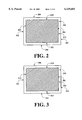
- FIG. 3 is a top view illustrating a faceplate in accordance with the present claimed invention.
- FIG. 4 is a top view illustrating a backplate after low temperature glass frit has been deposited thereover in accordance with the present claimed invention.
- FIG. 5 is a side view of a flat panel display in accordance with the present claimed invention.
- FIG. 6 is a top view illustrating a backplate after low temperature glass frit and a frame have been deposited thereover in accordance with a second embodiment of the present claimed invention.
- FIG. 7 is a side view of a flat panel display in accordance with a second embodiment of the present claimed invention.
- a faceplate is formed by depositing phosphor onto a glass plate.
- the phosphor is deposited onto the glass plate so as to form an active area.
- FIG. 2 shows faceplate 201 which has side surfaces 203-206.
- the phosphor is deposited so as to form active area 202.
- Active area 202 does not cover the entire surface area of faceplate 201.
- Side surfaces 210-213 of active area 202 are separated from side surfaces 203-206 of faceplate 201 so as to allow for sealing of faceplate 201 to, for example, a backplate.
- FIG. 3 shows backplate 301 to include active area 302 which includes side surfaces 310-313.
- backplate 301 is a glass plate onto which successive layers of material have been deposited so as to form cathodic structures within active area 302. These cathodic structures include emitters that emit high energy electrons. Spacers (not shown) may be attached to the backplate or the faceplate so as to give uniform spacing between the backplate and the faceplate. Structures such as electrical traces extend out of the active area. These structures are covered with a layer of dielectric such as an oxide layer so as to prevent shorting.
- a getter is deposited or placed on either faceplate 201 of FIG. 2 or on backplate 301 of FIG. 3.
- the getter is typically an evaporated metal such as Barium or non-evaporated metallic stripes such as zirconium.
- the getter absorbs certain gasses emitted during the heating step so as to reduce damage caused by outgassing.
- low temperature glass frit is deposited over the backplate as shown by step 101 of FIG. 1.
- the low temperature glass frit is deposited using a nozzle dispenser.
- the glass frit may be deposited using screen printing.
- the low temperature glass frit bar or frame is formed prior to deposition. Methods of forming low temperature glass frit bar or frame so as to obtain the desired shape and thickness include tape casting, molding, and extruding.
- the low temperature glass frit is formed by mixing 2 percent to 4 percent by weight Q-Pac organic compound with NEG low temperature glass.
- Q-pac organic compound may be purchased from Pac Polymer of Delaware and NEG low temperature glass may be purchased from Nippon Electrical Glass of Ostu, Japan.
- the resulting low temperature glass frit has a glass transition temperature of 200-250 degrees centigrade.
- low temperature glass frit 400 is deposited outside of active area 202 between side surfaces 210-213 and side surfaces 210-206. Traces which extend out from the active area (not shown) are covered by a dielectric layer to prevent shorting where they cross low temperature glass frit 400.
- the faceplate is then placed over the backplate as shown by step 102 of FIG. 1.
- the placement of the faceplate over the backplate is performed so as to align active area 302 of FIG. 3 with active area 202 of FIG. 2.
- FIG. 5 shows faceplate 301 placed over backplate 201 such that low temperature glass frit 400 is disposed between backplate 201 and faceplate 301, forming display assembly 500.
- display assembly 500 is placed in a vacuum.
- display assembly 500 is placed in an oven and the air is evacuated from the oven so as to produce a vacuum of 10 -7 torr.
- Heat is applied to the assembly as is shown by step 104 of FIG. 1.
- heat is applied by engaging the oven.
- the heat can be provided by laser or IR source. Both set up with laser and IR lamp have been successfully tested.
- the heat melts the glass frit and bonds the faceplate to the backplate.
- a temperature of 220 degrees centigrade is used.
- the heat is then disengaged. Once the glass frit has cooled sufficiently so as to produce an airtight seal, air is allowed to enter the oven, and the display assembly is removed from the oven.
- low temperature glass frit 400 has a thickness of approximately 50 mils prior to heating, giving a thickness of 30-40 mils after completion of the heating step. The melting of glass frit 400 forms an enclosure which is hermetically sealed.
- any temperature over the bias temperature of 200 degrees centigrade will melt the low temperature glass frit 400 of FIG. 4. Though it is desirable to keep the temperature as low as possible, the temperature must be high enough to efficiently melt low temperature glass frit 400 so as to minimize cycle time.
- the low bias temperature of low temperature glass frit 400 allows for melting at temperatures far below the prior art bias temperatures of 400 degrees centigrade. Thus, temperatures in the range of less than 300 degrees centigrade and above the bias temperature of 200 degrees centigrade allow for effective sealing of display assembly 500 of FIG. 5.
- the sealing process may be performed in a vacuum without disassociating the glass structure to produce unwanted lead and oxygen.
- a melting temperature of 220 degrees centigrade is used. However, due to process variations, and materials requirements, the temperature may be varied within a range of plus or minus 10 degrees centigrade.
- a vacuum is applied to the assembly by placing the assembly into a vacuum chamber and evacuating the gas within the vacuum chamber.
- heat is applied to the assembly by a laser or lamps emitting IR which is directed at the low temperature glass frit.
- the display assembly is heated to a temperature equal to the bias temperature of the glass of the faceplate and the backplate. This temperature is typically 300 degrees centigrade.
- FIGS. 6-7 Yet another embodiment of the present invention is shown in FIGS. 6-7 which includes frame 600.
- Spacer 600 is placed between side surfaces 210-213 of active area 202 and side surfaces 203-206 of backplate 201 so as to allow for a more precise control of the spacing between faceplate 301 and backplate 201.
- frame 600 is formed of ceramic material having a thickness of 35-40 mils. However a number of other materials with matching CTE could be used, such as glass, etc, as the frame materials.
- Low temperature glass frit is placed above and below frame 600 and the faceplate is placed over the backplate so as to form display assembly 700 as shown in FIG. 7.
- Layer of low temperature glass frit 701 of FIG. 7 is placed below frame 600 such that it is dispensed between frame 600 and backplate 201.
- layer of low temperature glass frit 702 is placed over frame 600 such that it is dispensed between frame 600 and faceplate 301.
- low temperature glass frit layer 701 and low temperature glass frit layer 702 have a thickness of approximately 7-8 mils and frame 600 has a thickness of approximately 35-40 mils.
- Display assembly 700 is then placed in an oven and the air is evacuated from the oven. The oven is then engaged so as to apply heat to display assembly 700, melting the glass frit.
- the present invention could be assembled starting with the faceplate.
- the glass frit is placed over the faceplate and the backplate is placed over the faceplate so as to obtain a display assembly.
- a first layer of glass frit is deposited over the faceplate and a frame is placed over the low temperature glass frit.
- a second layer of low temperature glass frit is then deposited on the other side of the frame and the backplate is placed over the faceplate.
- the present invention eliminates the prior art process steps of placing an evacuation tube across the glass frit, attaching a vacuum hose to the evacuation tube, evacuating the display through the evacuation tube, sealing off the evacuation tube, and removing the vacuum hose. These steps take up valuable manufacturing processing time and decrease throughput. Thus, by eliminating these steps, the present invention increases throughput and decreases manufacturing cost.
- the present invention eliminates the high temperature heating step of prior art manufacturing processes.
- the sealing temperature of the present invention (220 degrees centigrade) is significantly lower than the temperature of prior art sealing processes. This enables the sealing process to be performed in a vacuum without the decomposition of the glass frit into lead and oxygen.
- the lower temperature significantly lowers outgassing and reduces thermal degradation of the cathode. The reduction in outgassing and thermal stress reduces the number of defects and increases yield.
- the use of a lower temperature sealing process decreases cycle time and reduces stress on both the faceplate and the backplate.
Abstract
Description
Claims (14)
Priority Applications (5)
| Application Number | Priority Date | Filing Date | Title |
|---|---|---|---|
| US08/881,882 US6129603A (en) | 1997-06-24 | 1997-06-24 | Low temperature glass frit sealing for thin computer displays |
| EP98930209A EP0992055A4 (en) | 1997-06-24 | 1998-06-18 | Low temperature glass frit sealing for thin computer displays |
| PCT/US1998/012353 WO1998059357A1 (en) | 1997-06-24 | 1998-06-18 | Low temperature glass frit sealing for thin computer displays |
| KR10-1999-7012156A KR100525500B1 (en) | 1997-06-24 | 1998-06-18 | Low temperature glass frit sealing for thin computer displays |
| JP50461599A JP4323573B2 (en) | 1997-06-24 | 1998-06-18 | Manufacturing method of flat panel display device |
Applications Claiming Priority (1)
| Application Number | Priority Date | Filing Date | Title |
|---|---|---|---|
| US08/881,882 US6129603A (en) | 1997-06-24 | 1997-06-24 | Low temperature glass frit sealing for thin computer displays |
Publications (1)
| Publication Number | Publication Date |
|---|---|
| US6129603A true US6129603A (en) | 2000-10-10 |
Family
ID=25379391
Family Applications (1)
| Application Number | Title | Priority Date | Filing Date |
|---|---|---|---|
| US08/881,882 Expired - Lifetime US6129603A (en) | 1997-06-24 | 1997-06-24 | Low temperature glass frit sealing for thin computer displays |
Country Status (5)
| Country | Link |
|---|---|
| US (1) | US6129603A (en) |
| EP (1) | EP0992055A4 (en) |
| JP (1) | JP4323573B2 (en) |
| KR (1) | KR100525500B1 (en) |
| WO (1) | WO1998059357A1 (en) |
Cited By (23)
| Publication number | Priority date | Publication date | Assignee | Title |
|---|---|---|---|---|
| US20020063522A1 (en) * | 2000-11-29 | 2002-05-30 | Lg Electronics Inc. | Plasma display panel and method for fabricating the same |
| KR100352160B1 (en) * | 1999-11-16 | 2002-09-12 | 권상직 | Method of manufacturing a sealing paste for manufacturing a flat display panel in a vacuum and a method for sealing a flat display panel by using the sealing paste |
| US6534912B1 (en) * | 1998-05-20 | 2003-03-18 | Futaba Corporation | Active matrix drive fluorescent display device and method for manufacturing same |
| US6533632B1 (en) * | 1999-02-18 | 2003-03-18 | Micron Technology, Inc. | Method of evacuating and sealing flat panel displays and flat panel displays using same |
| US6545410B1 (en) * | 2000-07-21 | 2003-04-08 | Au Optronics Corp. | Flat panel display of a sealing channel |
| US6547618B1 (en) * | 2000-09-05 | 2003-04-15 | Motorola, Inc. | Seal and method of sealing field emission devices |
| US20030121591A1 (en) * | 2001-12-31 | 2003-07-03 | Kim Sung Ju | Method of joining substrates of flat plate display element |
| US6659828B1 (en) * | 1998-04-20 | 2003-12-09 | Patent-Treuhand-Gesellshaft Fuer Elektrische Gluehlampen Mbh | Flat discharge lamp and method for the production thereof |
| US20040161789A1 (en) * | 2000-08-30 | 2004-08-19 | Tanner Cameron W. | Porous inorganic substrate for high-density arrays |
| US20040164679A1 (en) * | 1998-08-09 | 2004-08-26 | Junichi Hibino | Display panel and manufacturing method for the same including improved bonding agent application method |
| US6817917B1 (en) * | 1999-05-28 | 2004-11-16 | Matsushita Electric Industrial Co., Ltd. | Manufacturing method for a plasma display panel with superior luminescence |
| US20050094242A1 (en) * | 2003-11-01 | 2005-05-05 | Fusao Ishii | Vacuum packaged micromirror arrays and methods of manufacturing the same |
| US20060082298A1 (en) * | 2004-10-20 | 2006-04-20 | Becken Keith J | Optimization of parameters for sealing organic emitting light diode (OLED) displays |
| US20070128967A1 (en) * | 2005-12-06 | 2007-06-07 | Becken Keith J | Method of making a glass envelope |
| US20070128966A1 (en) * | 2005-12-06 | 2007-06-07 | Becken Keith J | Method of encapsulating a display element |
| US20070241085A1 (en) * | 2006-03-27 | 2007-10-18 | Nec Corporation | Laser cutting method, display apparatus manufacturing method, and display apparatus |
| US20090058292A1 (en) * | 2007-08-27 | 2009-03-05 | Koo Won-Hoe | Flat panel display and fabricating method thereof |
| US20090189230A1 (en) * | 2004-09-27 | 2009-07-30 | Idc, Llc | Method and system for packaging mems devices with incorporated getter |
| US20090298999A1 (en) * | 2006-02-16 | 2009-12-03 | Northwestern University | Modified Acrylic Block Copolymers For Hydrogels and Pressure Sensitive Wet Adhesives |
| US20100304513A1 (en) * | 2009-05-28 | 2010-12-02 | Kelvin Nguyen | Method for forming an organic light emitting diode device |
| DE102005003257B4 (en) * | 2004-01-26 | 2011-02-10 | Futaba Corp., Mobara-shi | Fluorescence display element with improved gas absorption |
| CN101490853B (en) * | 2006-06-15 | 2011-11-23 | 荷兰能源建设基金中心 | Solar panel and associated method |
| US8448468B2 (en) | 2008-06-11 | 2013-05-28 | Corning Incorporated | Mask and method for sealing a glass envelope |
Families Citing this family (5)
| Publication number | Priority date | Publication date | Assignee | Title |
|---|---|---|---|---|
| US6113450A (en) * | 1998-05-14 | 2000-09-05 | Candescent Technologies Corporation | Seal material frit frame for flat panel displays |
| WO2000060634A1 (en) * | 1999-03-31 | 2000-10-12 | Kabushiki Kaisha Toshiba | Method for manufacturing flat image display and flat image display |
| DE19936864A1 (en) | 1999-08-05 | 2001-02-15 | Patent Treuhand Ges Fuer Elektrische Gluehlampen Mbh | Method for inserting a pump stem into a discharge vessel |
| WO2001054158A1 (en) * | 2000-01-21 | 2001-07-26 | Ceravision Technology Limited | Visual display |
| KR100657403B1 (en) * | 2004-11-10 | 2006-12-14 | 주식회사 멤스웨어 | Method for sealing of organic electro-luminescence device |
Citations (4)
| Publication number | Priority date | Publication date | Assignee | Title |
|---|---|---|---|---|
| US4058387A (en) * | 1975-07-03 | 1977-11-15 | Owens-Illinois, Inc. | Simultaneously baking and sealing a faceplate assembly |
| US5424605A (en) * | 1992-04-10 | 1995-06-13 | Silicon Video Corporation | Self supporting flat video display |
| US5688708A (en) * | 1996-06-24 | 1997-11-18 | Motorola | Method of making an ultra-high vacuum field emission display |
| US5697825A (en) * | 1995-09-29 | 1997-12-16 | Micron Display Technology, Inc. | Method for evacuating and sealing field emission displays |
Family Cites Families (4)
| Publication number | Priority date | Publication date | Assignee | Title |
|---|---|---|---|---|
| US3778126A (en) * | 1971-12-30 | 1973-12-11 | Ibm | Gas display panel without exhaust tube structure |
| JPH07226175A (en) * | 1994-02-10 | 1995-08-22 | Matsushita Electric Ind Co Ltd | Vaccum vessel for thin type display device |
| US5448131A (en) * | 1994-04-13 | 1995-09-05 | Texas Instruments Incorporated | Spacer for flat panel display |
| JPH09511613A (en) * | 1994-11-09 | 1997-11-18 | ピクステク ソシエテ アノニム | Flat display screen assembly method |
-
1997
- 1997-06-24 US US08/881,882 patent/US6129603A/en not_active Expired - Lifetime
-
1998
- 1998-06-18 EP EP98930209A patent/EP0992055A4/en not_active Withdrawn
- 1998-06-18 JP JP50461599A patent/JP4323573B2/en not_active Expired - Fee Related
- 1998-06-18 WO PCT/US1998/012353 patent/WO1998059357A1/en active IP Right Grant
- 1998-06-18 KR KR10-1999-7012156A patent/KR100525500B1/en not_active IP Right Cessation
Patent Citations (4)
| Publication number | Priority date | Publication date | Assignee | Title |
|---|---|---|---|---|
| US4058387A (en) * | 1975-07-03 | 1977-11-15 | Owens-Illinois, Inc. | Simultaneously baking and sealing a faceplate assembly |
| US5424605A (en) * | 1992-04-10 | 1995-06-13 | Silicon Video Corporation | Self supporting flat video display |
| US5697825A (en) * | 1995-09-29 | 1997-12-16 | Micron Display Technology, Inc. | Method for evacuating and sealing field emission displays |
| US5688708A (en) * | 1996-06-24 | 1997-11-18 | Motorola | Method of making an ultra-high vacuum field emission display |
Cited By (33)
| Publication number | Priority date | Publication date | Assignee | Title |
|---|---|---|---|---|
| US6659828B1 (en) * | 1998-04-20 | 2003-12-09 | Patent-Treuhand-Gesellshaft Fuer Elektrische Gluehlampen Mbh | Flat discharge lamp and method for the production thereof |
| US6534912B1 (en) * | 1998-05-20 | 2003-03-18 | Futaba Corporation | Active matrix drive fluorescent display device and method for manufacturing same |
| US20040164679A1 (en) * | 1998-08-09 | 2004-08-26 | Junichi Hibino | Display panel and manufacturing method for the same including improved bonding agent application method |
| US6860781B2 (en) * | 1998-09-08 | 2005-03-01 | Matsushita Electric Industrial Co., Ltd. | Display panel and manufacturing method for the same including improved bonding agent application method |
| US6533632B1 (en) * | 1999-02-18 | 2003-03-18 | Micron Technology, Inc. | Method of evacuating and sealing flat panel displays and flat panel displays using same |
| US6817917B1 (en) * | 1999-05-28 | 2004-11-16 | Matsushita Electric Industrial Co., Ltd. | Manufacturing method for a plasma display panel with superior luminescence |
| KR100352160B1 (en) * | 1999-11-16 | 2002-09-12 | 권상직 | Method of manufacturing a sealing paste for manufacturing a flat display panel in a vacuum and a method for sealing a flat display panel by using the sealing paste |
| US6545410B1 (en) * | 2000-07-21 | 2003-04-08 | Au Optronics Corp. | Flat panel display of a sealing channel |
| US20040161789A1 (en) * | 2000-08-30 | 2004-08-19 | Tanner Cameron W. | Porous inorganic substrate for high-density arrays |
| US6547618B1 (en) * | 2000-09-05 | 2003-04-15 | Motorola, Inc. | Seal and method of sealing field emission devices |
| US6809476B2 (en) * | 2000-11-29 | 2004-10-26 | Lg Electronics Inc. | Plasma display panel and method for fabricating the same |
| US20020063522A1 (en) * | 2000-11-29 | 2002-05-30 | Lg Electronics Inc. | Plasma display panel and method for fabricating the same |
| US20030121591A1 (en) * | 2001-12-31 | 2003-07-03 | Kim Sung Ju | Method of joining substrates of flat plate display element |
| US20050094242A1 (en) * | 2003-11-01 | 2005-05-05 | Fusao Ishii | Vacuum packaged micromirror arrays and methods of manufacturing the same |
| US6903860B2 (en) | 2003-11-01 | 2005-06-07 | Fusao Ishii | Vacuum packaged micromirror arrays and methods of manufacturing the same |
| DE102005003257B4 (en) * | 2004-01-26 | 2011-02-10 | Futaba Corp., Mobara-shi | Fluorescence display element with improved gas absorption |
| US20090189230A1 (en) * | 2004-09-27 | 2009-07-30 | Idc, Llc | Method and system for packaging mems devices with incorporated getter |
| US8735225B2 (en) * | 2004-09-27 | 2014-05-27 | Qualcomm Mems Technologies, Inc. | Method and system for packaging MEMS devices with glass seal |
| US20060082298A1 (en) * | 2004-10-20 | 2006-04-20 | Becken Keith J | Optimization of parameters for sealing organic emitting light diode (OLED) displays |
| US7371143B2 (en) * | 2004-10-20 | 2008-05-13 | Corning Incorporated | Optimization of parameters for sealing organic emitting light diode (OLED) displays |
| US20070128967A1 (en) * | 2005-12-06 | 2007-06-07 | Becken Keith J | Method of making a glass envelope |
| US7537504B2 (en) | 2005-12-06 | 2009-05-26 | Corning Incorporated | Method of encapsulating a display element with frit wall and laser beam |
| US7597603B2 (en) | 2005-12-06 | 2009-10-06 | Corning Incorporated | Method of encapsulating a display element |
| US20070128966A1 (en) * | 2005-12-06 | 2007-06-07 | Becken Keith J | Method of encapsulating a display element |
| US20090298999A1 (en) * | 2006-02-16 | 2009-12-03 | Northwestern University | Modified Acrylic Block Copolymers For Hydrogels and Pressure Sensitive Wet Adhesives |
| US20070241085A1 (en) * | 2006-03-27 | 2007-10-18 | Nec Corporation | Laser cutting method, display apparatus manufacturing method, and display apparatus |
| US8791387B2 (en) * | 2006-03-27 | 2014-07-29 | Nlt Technologies, Ltd. | Laser cutting method, display apparatus manufacturing method, and display apparatus |
| CN101490853B (en) * | 2006-06-15 | 2011-11-23 | 荷兰能源建设基金中心 | Solar panel and associated method |
| US20090058292A1 (en) * | 2007-08-27 | 2009-03-05 | Koo Won-Hoe | Flat panel display and fabricating method thereof |
| US8448468B2 (en) | 2008-06-11 | 2013-05-28 | Corning Incorporated | Mask and method for sealing a glass envelope |
| US9399594B2 (en) | 2008-06-11 | 2016-07-26 | Corning Incorporated | Mask and method for sealing a glass envelope |
| US20100304513A1 (en) * | 2009-05-28 | 2010-12-02 | Kelvin Nguyen | Method for forming an organic light emitting diode device |
| US8440479B2 (en) | 2009-05-28 | 2013-05-14 | Corning Incorporated | Method for forming an organic light emitting diode device |
Also Published As
| Publication number | Publication date |
|---|---|
| WO1998059357A1 (en) | 1998-12-30 |
| EP0992055A4 (en) | 2002-06-19 |
| KR20010020487A (en) | 2001-03-15 |
| JP4323573B2 (en) | 2009-09-02 |
| JP2002505796A (en) | 2002-02-19 |
| EP0992055A1 (en) | 2000-04-12 |
| KR100525500B1 (en) | 2005-11-01 |
Similar Documents
| Publication | Publication Date | Title |
|---|---|---|
| US6129603A (en) | Low temperature glass frit sealing for thin computer displays | |
| US6113450A (en) | Seal material frit frame for flat panel displays | |
| US6565400B1 (en) | Frit protection in sealing process for flat panel displays | |
| US6037710A (en) | Microwave sealing of flat panel displays | |
| US6140762A (en) | Wall assembly and method for attaching walls for flat panel displays | |
| US5820435A (en) | Gap jumping to seal structure including tacking of structure | |
| US6827621B1 (en) | Method and apparatus for manufacturing flat image display device | |
| US7714496B2 (en) | Field emission display device and field emission type backlight device having a sealing structure for vacuum exhaust | |
| KR100447130B1 (en) | Cap sealing method of field emission display and fabricating method thereof | |
| KR20070007843A (en) | Method of producing image display device | |
| JP3940577B2 (en) | Flat display device and manufacturing method thereof | |
| KR20040066190A (en) | Image display device and its manufacturing method | |
| JP3940583B2 (en) | Flat display device and manufacturing method thereof | |
| JP2002100311A (en) | Picture display device and its manufacturing method | |
| KR100769383B1 (en) | Image display device and method of producing the device | |
| JP2003132822A (en) | Panel display device and manufacturing method therefor | |
| US6632117B1 (en) | Frit protection in sealing process for flat panel displays | |
| JP2002358915A (en) | Image display device | |
| US20070103051A1 (en) | Image display apparatus | |
| JP2004013067A (en) | Image display device | |
| JP2000251793A (en) | Airtight container and image display device | |
| WO2006035607A1 (en) | Method and apparatus for manufacturing image display device | |
| JPH0668799A (en) | Manufacture of display device | |
| JP2002033046A (en) | Image display device and method of manufacturing the same | |
| JP2007335363A (en) | Image display device |
Legal Events
| Date | Code | Title | Description |
|---|---|---|---|
| AS | Assignment |
Owner name: CANDESCENT TECHNOLOGIES, INC., CALIFORNIA Free format text: ASSIGNMENT OF ASSIGNORS INTEREST;ASSIGNORS:SUN, JENNIFER Y.;MA, YUTAO;REEL/FRAME:008671/0145 Effective date: 19970624 |
|
| STCF | Information on status: patent grant |
Free format text: PATENTED CASE |
|
| AS | Assignment |
Owner name: CANDESCENT INTELLECTUAL PROPERTY SERVICES, INC., C Free format text: ASSIGNMENT OF ASSIGNORS INTEREST;ASSIGNOR:CANDESCENT TECHNOLOGIES CORPORATION;REEL/FRAME:011821/0569 Effective date: 20001205 |
|
| AS | Assignment |
Owner name: UNITED STATES GOVERNMENT DEFENSE CONTRACT MANAGEME Free format text: CONFIRMATORY LICENSE;ASSIGNOR:CANDESCENT TECHNOLOGIES CORPORATION;REEL/FRAME:013221/0444 Effective date: 20010907 |
|
| FPAY | Fee payment |
Year of fee payment: 4 |
|
| AS | Assignment |
Owner name: DARPA, VIRGINIA Free format text: CONFIRMATORY LICENSE;ASSIGNOR:CANDESCENT TECHNOLOGIES CORPORATION;REEL/FRAME:015788/0417 Effective date: 20040913 |
|
| AS | Assignment |
Owner name: CANDESCENT TECHNOLOGIES CORPORATION, CALIFORNIA Free format text: CORRECTIVE ASSIGNMENT TO CORRECT THE ASSIGNEE. THE NAME OF THE ASSIGNEE WAS INCORRECTLY LISTED ON THE RECORDATION FORM COVER SHEET PREVIOUSLY RECORDED ON REEL 008671 FRAME 0145;ASSIGNORS:SUN, JENNIFER Y.;MA, YUTAO;REEL/FRAME:018492/0800 Effective date: 19970624 |
|
| AS | Assignment |
Owner name: CANON KABUSHIKI KAISHA, JAPAN Free format text: NUNC PRO TUNC ASSIGNMENT EFFECTIVE AS OF AUGUST 26, 2004;ASSIGNOR:CANDESCENT TECHNOLOGIES CORPORATION;REEL/FRAME:019466/0437 Effective date: 20070104 |
|
| AS | Assignment |
Owner name: CANON KABUSHIKI KAISHA, JAPAN Free format text: NUNC PRO TUNC ASSIGNMENT;ASSIGNOR:CANDESCENT INTELLECTUAL PROPERTY SERVICES, INC.;REEL/FRAME:019580/0723 Effective date: 20061226 |
|
| AS | Assignment |
Owner name: CANDESCENT TECHNOLOGIES CORPORATION, CALIFORNIA Free format text: CORRECTIVE ASSIGNMENT TO CORRECT THE ASSIGNEE. THE NAME OF ONE ASSIGNEE WAS INADVERTENTLY OMITTED FROM THE RECORDATION FORM COVER SHEET PREVIOUSLY RECORDED ON REEL 011821 FRAME 0569;ASSIGNOR:CANDESCENT TECHNOLOGIES CORPORATION;REEL/FRAME:019679/0375 Effective date: 20001205 Owner name: CANDESCENT INTELLECTUAL PROPERTY SERVICES, INC., C Free format text: CORRECTIVE ASSIGNMENT TO CORRECT THE ASSIGNEE. THE NAME OF ONE ASSIGNEE WAS INADVERTENTLY OMITTED FROM THE RECORDATION FORM COVER SHEET PREVIOUSLY RECORDED ON REEL 011821 FRAME 0569;ASSIGNOR:CANDESCENT TECHNOLOGIES CORPORATION;REEL/FRAME:019679/0375 Effective date: 20001205 |
|
| FPAY | Fee payment |
Year of fee payment: 8 |
|
| FPAY | Fee payment |
Year of fee payment: 12 |