US5844208A - Temperature control system for an electronic device in which device temperature is estimated from heater temperature and heat sink temperature - Google Patents
Temperature control system for an electronic device in which device temperature is estimated from heater temperature and heat sink temperature Download PDFInfo
- Publication number
- US5844208A US5844208A US08/833,368 US83336897A US5844208A US 5844208 A US5844208 A US 5844208A US 83336897 A US83336897 A US 83336897A US 5844208 A US5844208 A US 5844208A
- Authority
- US
- United States
- Prior art keywords
- temperature
- heater
- electronic device
- control system
- face
- Prior art date
- Legal status (The legal status is an assumption and is not a legal conclusion. Google has not performed a legal analysis and makes no representation as to the accuracy of the status listed.)
- Expired - Lifetime
Links
Images


Classifications
-
- G—PHYSICS
- G01—MEASURING; TESTING
- G01R—MEASURING ELECTRIC VARIABLES; MEASURING MAGNETIC VARIABLES
- G01R31/00—Arrangements for testing electric properties; Arrangements for locating electric faults; Arrangements for electrical testing characterised by what is being tested not provided for elsewhere
- G01R31/28—Testing of electronic circuits, e.g. by signal tracer
- G01R31/2851—Testing of integrated circuits [IC]
- G01R31/2855—Environmental, reliability or burn-in testing
- G01R31/2872—Environmental, reliability or burn-in testing related to electrical or environmental aspects, e.g. temperature, humidity, vibration, nuclear radiation
- G01R31/2874—Environmental, reliability or burn-in testing related to electrical or environmental aspects, e.g. temperature, humidity, vibration, nuclear radiation related to temperature
-
- G—PHYSICS
- G01—MEASURING; TESTING
- G01R—MEASURING ELECTRIC VARIABLES; MEASURING MAGNETIC VARIABLES
- G01R31/00—Arrangements for testing electric properties; Arrangements for locating electric faults; Arrangements for electrical testing characterised by what is being tested not provided for elsewhere
- G01R31/28—Testing of electronic circuits, e.g. by signal tracer
- G01R31/2851—Testing of integrated circuits [IC]
- G01R31/2886—Features relating to contacting the IC under test, e.g. probe heads; chucks
- G01R31/2891—Features relating to contacting the IC under test, e.g. probe heads; chucks related to sensing or controlling of force, position, temperature
-
- G—PHYSICS
- G05—CONTROLLING; REGULATING
- G05D—SYSTEMS FOR CONTROLLING OR REGULATING NON-ELECTRIC VARIABLES
- G05D23/00—Control of temperature
- G05D23/19—Control of temperature characterised by the use of electric means
- G05D23/1919—Control of temperature characterised by the use of electric means characterised by the type of controller
- G05D23/192—Control of temperature characterised by the use of electric means characterised by the type of controller using a modification of the thermal impedance between a source and the load
-
- H—ELECTRICITY
- H01—ELECTRIC ELEMENTS
- H01L—SEMICONDUCTOR DEVICES NOT COVERED BY CLASS H10
- H01L23/00—Details of semiconductor or other solid state devices
- H01L23/34—Arrangements for cooling, heating, ventilating or temperature compensation ; Temperature sensing arrangements
-
- H—ELECTRICITY
- H01—ELECTRIC ELEMENTS
- H01L—SEMICONDUCTOR DEVICES NOT COVERED BY CLASS H10
- H01L23/00—Details of semiconductor or other solid state devices
- H01L23/34—Arrangements for cooling, heating, ventilating or temperature compensation ; Temperature sensing arrangements
- H01L23/345—Arrangements for heating
-
- H—ELECTRICITY
- H01—ELECTRIC ELEMENTS
- H01L—SEMICONDUCTOR DEVICES NOT COVERED BY CLASS H10
- H01L23/00—Details of semiconductor or other solid state devices
- H01L23/34—Arrangements for cooling, heating, ventilating or temperature compensation ; Temperature sensing arrangements
- H01L23/42—Fillings or auxiliary members in containers or encapsulations selected or arranged to facilitate heating or cooling
-
- H—ELECTRICITY
- H01—ELECTRIC ELEMENTS
- H01L—SEMICONDUCTOR DEVICES NOT COVERED BY CLASS H10
- H01L2224/00—Indexing scheme for arrangements for connecting or disconnecting semiconductor or solid-state bodies and methods related thereto as covered by H01L24/00
- H01L2224/01—Means for bonding being attached to, or being formed on, the surface to be connected, e.g. chip-to-package, die-attach, "first-level" interconnects; Manufacturing methods related thereto
- H01L2224/10—Bump connectors; Manufacturing methods related thereto
- H01L2224/15—Structure, shape, material or disposition of the bump connectors after the connecting process
- H01L2224/16—Structure, shape, material or disposition of the bump connectors after the connecting process of an individual bump connector
-
- H—ELECTRICITY
- H01—ELECTRIC ELEMENTS
- H01L—SEMICONDUCTOR DEVICES NOT COVERED BY CLASS H10
- H01L2224/00—Indexing scheme for arrangements for connecting or disconnecting semiconductor or solid-state bodies and methods related thereto as covered by H01L24/00
- H01L2224/73—Means for bonding being of different types provided for in two or more of groups H01L2224/10, H01L2224/18, H01L2224/26, H01L2224/34, H01L2224/42, H01L2224/50, H01L2224/63, H01L2224/71
- H01L2224/732—Location after the connecting process
- H01L2224/73251—Location after the connecting process on different surfaces
- H01L2224/73253—Bump and layer connectors
-
- H—ELECTRICITY
- H01—ELECTRIC ELEMENTS
- H01L—SEMICONDUCTOR DEVICES NOT COVERED BY CLASS H10
- H01L2924/00—Indexing scheme for arrangements or methods for connecting or disconnecting semiconductor or solid-state bodies as covered by H01L24/00
- H01L2924/01—Chemical elements
- H01L2924/01046—Palladium [Pd]
-
- H—ELECTRICITY
- H01—ELECTRIC ELEMENTS
- H01L—SEMICONDUCTOR DEVICES NOT COVERED BY CLASS H10
- H01L2924/00—Indexing scheme for arrangements or methods for connecting or disconnecting semiconductor or solid-state bodies as covered by H01L24/00
- H01L2924/10—Details of semiconductor or other solid state devices to be connected
- H01L2924/11—Device type
- H01L2924/13—Discrete devices, e.g. 3 terminal devices
- H01L2924/1304—Transistor
- H01L2924/1305—Bipolar Junction Transistor [BJT]
-
- H—ELECTRICITY
- H01—ELECTRIC ELEMENTS
- H01L—SEMICONDUCTOR DEVICES NOT COVERED BY CLASS H10
- H01L2924/00—Indexing scheme for arrangements or methods for connecting or disconnecting semiconductor or solid-state bodies as covered by H01L24/00
- H01L2924/10—Details of semiconductor or other solid state devices to be connected
- H01L2924/11—Device type
- H01L2924/14—Integrated circuits
Definitions
- This invention relates to temperature control systems which maintain the temperature of an electronic device near a constant set point temperature while the device is being tested; and it relates to subassemblies which comprise key portions of such temperature control systems.
- circuitry can be integrated into the chips, such as digital logic circuitry or memory circuitry or analog circuitry.
- the circuitry in the chips can be comprised of any type of transistors, such as field effect transistors or bipolar transistors.
- CMOS transistors complementary field effect transistors
- CMOS memory chips and CMOS microprocessor chips are processed in this fashion. However, in order to determine the speed of such chips properly, the temperature of each chip must be kept nearly constant while the speed test is performed.
- Maintaining the chip temperature near a constant set point is quite simple if the instantaneous power dissipation of the chip is constant or varies in a small range while the speed test is being performed. In that case, it is only necessary to couple the chip through a fixed thermal resistance to a thermal mass which is at a fixed temperature. For example, if the maximum chip power variation is ten watts, and the coupling between the chip and the thermal mass is 0.2° C./watt, then the chip temperature will vary a maximum of 2° C.
- CMOS chips because their instantaneous power dissipation increases as the number of CMOS transistors which are switching ON or OFF increases.
- the number of transistors which are switching is always changing; thus, the chip's power dissipation and temperature and speed are always changing.
- the magnitude of these changes increases as more transistors get integrated into a single chip, because the number of transistors which are switching at any particular instant will vary from none to all of the transistors on the chip.
- the chip temperature is increased or lowered by directing a temperature controlled gas jet at the chip or immersing the chip in a temperature controlled liquid.
- these control systems are limited by the speed at which the temperature of the gas jet or liquid can be increased or decreased.
- FIG. 7 a control system is disclosed in FIG. 7 which includes both a heater for heating the chip and a liquid cooled aluminum block for cooling the chip.
- FIG. 7 control system still is not capable of enabling speed tests to be run on chips which widely vary their power dissipation during the test, because it cannot react fast enough to compensate for such power variations. Why this deficiency occurs is explained herein in detail in conjunction with FIGS. 8, 9, and 10.
- a primary object of the inventions which are disclosed herein is to provide novel temperature control systems, and novel subassemblies for such systems, which react quickly to large variations in power dissipation within an electronic device and thereby maintain the device temperature near a constant set point temperature while the device is being tested.
- the estimator circuit enables the system to operate with electronic devices that do not have a temperature sensor.
- Another major feature of this system is that by electrically controlling just the heater power, heat flow to/from the electronic device is quickly adjusted; and that in turn quickly regulates the device temperature.
- FIG. 1 shows a temperature control system which constitutes a preferred embodiment of the invention having Docket No. 550,577.
- FIG. 2 is a schematic diagram which helps explain the operation of the FIG. 1 temperature control system.
- FIG. 3 replicates the schematic diagram of FIG. 2 and depicts the operation of the FIG. 1 control system for the case where the power dissipation in the electronic device steps up.
- FIG. 4 replicates the schematic diagram of FIG. 2 and depicts the operation of the FIG. 1 control system for the case where the power dissipation in the electronic device steps down.
- FIG. 5 is a set of differential equations which precisely defines the behavior of the FIG. 1 control system.
- FIG. 6 shows how several parameters vary in the FIG. 1 control system when that system is simulated via the FIG. 5 equations.
- FIG. 7 shows how several additional parameters vary in the FIG. 1 control system when that system is simulated via the FIG. 5 equations.
- FIG. 8 is a schematic diagram, similar to the schematic diagram of FIG. 2, which helps explain the operation of a prior art temperature control system that is described in U.S. Pat. No. 5,420,521.
- FIG. 9 is a set of differential equations which precisely defines the behavior of the FIG. 8 temperature control system and help explain a distinguishing feature between the operation of the control systems of FIGS. 1 and 8.
- FIG. 10 is a set of differential equations which helps explain another distinguishing feature between the operation of the control systems of FIGS. 1 and 8.
- FIG. 11 is a set of differential equations which forms the basis of the temperature control system having Docket 550,578.
- FIG. 12 shows a preferred embodiment of the temperature control system which is based on the FIG. 11 equations.
- FIG. 13 is a set of curves which is obtained by a simulation of the FIG. 12 temperature control system.
- FIG. 14 is another set of curves which is obtained by a second simulation of the FIG. 12 temperature control system in which a particular parameter is injected with an error.
- FIG. 15 lists the steps of a process by which the error in the parameter of FIG. 14 can be detected and corrected.
- FIG. 16 illustrates how the FIG. 15 process is carried out.
- FIG. 17 shows an initial stage of fabricating a subassembly which constitutes the invention having Docket No. 550,579.
- FIG. 18 shows how the subassembly of FIG. 17 is completed and incorporated into the temperature control systems of FIGS. 1 and 12.
- FIG. 19 shows how a film on an electronic device in the subassembly of FIG. 18 is removed.
- FIG. 20 shows a modification for a heater component within the temperature control systems of FIGS. 1 and 12.
- FIG. 21 shows a modification for the subassembly of FIG. 18.
- reference numeral 11 identifies an electronic device which is to be tested while its temperature is maintained near a constant set point.
- Two specific examples of this electronic device 11 are an integrated chip which is packaged in ceramic or plastic, or a bare chip which is unpackaged.
- Any type of circuitry which needs to be tested can be integrated into the electronic device 11, such as digital logic circuitry or memory circuitry or analog circuitry; and that circuitry can be comprised of any type of transistors, such as N-channel field effect transistors or P-channel field effect transistors or complimentary field effect transistors or bi-polar transistors.
- the electronic device 11 includes dozens of input/output terminals 11a; but for simplicity in FIG. 1, only a few of those terminals are shown. These terminals 11a are coupled to three sets of signal lines 12a, 12b, and 12c. On the signal lines 12a, input signals “TEST-IN” are received which test the electronic device 11; and on the signal lines 12b, output signals “TESTOUT” are sent from the electronic device 11 as a response to the test. Conventional test equipment (not shown) is coupled to the signal lines 12a and 12b to respectively send and receive the signals on those lines. On the signal lines 12c, output signals "TEMP" are sent from the electronic device 11 which indicate its temperature. These TEMP signals originate from a temperature sensor, such as a temperature sensitive resistor or diode, which is integrated into the electronic device.
- a temperature sensor such as a temperature sensitive resistor or diode
- All of the remaining components 12-17 in FIG. 1 constitute a temperature control system which keeps the temperature of the electronic device 11 near the set point while that device is being tested. Each component in this control system is described below in TABLE 1.
- the electronic device 11 In operation, the electronic device 11 varies in its power dissipation as it is being tested by the TEST-IN signals which it receives on the signal lines 12a. This variation in power occurs because the transistors in the electronic device 11 turn on and off, and thereby vary in their power dissipation, in response to the TEST-IN signals. Consequently, the temperature of the electronic device 11 tends to increase as its power dissipation increases; and vice-versa.
- a temperature sensor generates the TEMP signals on the signal lines 12c which indicate the present temperature of the device. Those TEMP signals are sent to the power regulator 16 where they are compared with the SET-POINT signals on the signal lines 12d. If the temperature of the device 11 is less than the set point temperature, then the regulator 16 generates the control signals CTL such that the variable power P h to the heater 13 is increased. Conversely, if the temperature of the device 11 is more than the set point temperature, then the regulator 16 generates the control signals CTL such that the variable power PWR to the heater 13 is decreased.
- FIGS. 2, 3 and 4 are schematic diagrams of the FIG. 1 control system wherein the electronic device 11 is coupled to the electric heater 13 through a thermal resistance ⁇ d-h ; the heater 13 is coupled to the heat sink base 14a through a thermal resistance ⁇ h-s ; and the heat sink base is coupled to the liquid coolant through a thermal resistance ⁇ S-L . Also in the FIGS. 2-4, the electronic device 11 receives and dissipates a variable amount of power P d , and the electric heater receives and dissipates a variable amount of power P h . Further in the FIGS.
- the electronic device 11 has a temperature T d and a thermal mass M d ; the heater 13 has a temperature T h and a thermal mass M h ; and the heat sink base 14a has a temperature T S and a thermal mass M s .
- the heater's thermal mass M h is made as small as is practical. This constraint, as will be shown below, helps to improve the speed with which the heater 13 can raise or lower its temperature, and thereby maintain the temperature T d of the electronic device near the set point.
- One suitable upper limit for the thermal mass M h is that it be no larger than three times the thermal mass M d of the electronic device; and preferably, M h is less than M d .
- the heater's thermal resistance ⁇ d-h is made as small as practical. This constraint, as will be shown below, helps to increase the amount of heat that is transferred from the heater 13 to the electronic device 11, relative to the amount of heat that is transferred from the heater 13 to the heat sink 14.
- a suitable upper limit for the thermal resistance ⁇ d-h is that it be no more than three times the thermal resistance ⁇ h-s between the heater and the heat sink base; and preferably, ⁇ d-h is less than ⁇ h-s .
- the electronic device 11 increases its power dissipation P d and thereby causes its temperature T d to rise above the set point. This is shown in FIG. 3 as occurring at time instants t1 and t2.
- the power P h to the heater 13 is reduced by the regulator 16; and this is shown in FIG. 3 as occurring at time t3.
- Heater 13 has a low thermal mass M h ; and consequently, the heater's temperature T h drops rapidly when the heater's power is reduced, as indicated at time t4.
- the heater temperature T d starts to cool down, as indicated at time t5.
- the heater power P h ramps up as indicated at time t6.
- the heater temperature T h rises and thereby reduces the flow of heat from the device 11 along the thermal path 21.
- the electronic device 11 decreases its power dissipation P d and thereby causes its temperature T d to drop below the set point. This is shown in FIG. 4 as occurring at time instants t1 and t2.
- the power P h to the heater 13 is increased by the regulator 16; and this is shown in FIG. 4 as occurring at time t3.
- Heater 13 has a low thermal mass M h ; and consequently, the heater's temperature T h rises rapidly when the heater's power is increased as indicated at time t4.
- the heater temperature T h rises so high that it exceeds the device temperature T d , one portion of the heat from the heater travels along the thermal path 22a in FIG. 4 to the electronic device 11, and another portion of the heat from the heater travels along the thermal path 22b to the liquid coolant. Also, the amount of heat which travels on path 22a to the electronic device 11 increases as ⁇ d-h decreases relative to ⁇ h-s .
- the device temperature T d starts to rise, as indicated at time t5.
- the heater power P h ramps down as indicated at time t6.
- the heater temperature T h ramps down and thereby reduces the flow of heat from the heater to the device 11 along the thermal path 22a.
- the heater 13 controls the amount of heat that flows on the paths 21 and 22a.
- T h equals T.sub., no heat flows on path 21 or 22a.
- T h is less than T d , then heat flows on path 21 from the electronic device through the heater 13 to the heat sink; and the rate of heat flow increases as T d -T h increases.
- T h is more than T d , then heat flows on path 22a from the heater 13 to the electronic device; and the rate of heat flow increases as T h -T d increases.
- P h heat flow to/from the electronic device is regulated; and that in turn regulates the device temperature.
- FIGS. 5, 6 and 7. three differential equations are provided which are labeled equation 1, equation 2, and equation 3. These equations are based on the principle that the sum of the thermal power which is received by a body is equal to the thermal mass of the body times the rate of change of the body's temperature.
- Equation 1 contains three terms which are identified by reference numerals 31a, 31b and 31c.
- Term 31a is the power which the electronic device 11 receives and dissipates in response to the TEST-IN signals;
- term 31b is the power which is transferred to the electronic device 11 through the thermal resistance ⁇ d-h ; and
- term 31c is the thermal mass of the electronic device 11 times the rate of change of its temperature.
- equation 2 contains four terms which are identified by reference numerals 32a, 32b, 32c, and 32d.
- Term 32a is the power which is supplied to the electric heater 13 from the variable power supply 17;
- term 32b is the power which is transferred to the electric heater 13 through the thermal resistance ⁇ h-a ;
- term 32c is the power which is transferred to the heater 13 through the thermal resistance ⁇ d-h ;
- term 32d is the thermal mass of the heater times the rate of change of the heater's temperature.
- equation 3 contains three terms which are identified by reference numerals 33a, 33b, and 33c.
- Term 33a is the power which is transferred to the heat sink base 14a through the thermal resistance ⁇ S-L ;
- term 33b is the power which is transferred to the heat sink base through the thermal resistance ⁇ h-s ;
- term 33c is the mass of the heat sink base times the rate of change of its temperature.
- FIG. 5 Using the three equations of FIG. 5, a simulation on a digital computer was performed; and the results of that simulation are shown in FIGS. 6 and 7. In performing this simulation, the various parameters in the FIG. 5 equations had the values which are shown below in TABLE 2.
- the simulation assumed that the electronic device 11 was initially at the set point temperature and was dissipating no power. Thereafter, at a time equal to two seconds, the power dissipation of the electronic device 11 was stepped up in response to the TEST-IN signals, to a power of 100 watts. This power dissipation remained constant in the electronic device 11 for three seconds at which time the power dissipation in the device 11 went back to zero.
- the thermal mass M d in TABLE 2 is the thermal mass of a bare integrated circuit chip; and thus, it constitutes another worst case test condition because its temperature will change temperature faster than the temperature of a packaged chip (which inherently has a larger thermal mass).
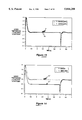
- Curve 41 in FIG. 6 shows how the power dissipation in the electronic device 11 changes with time, as described above. Also in FIGS. 6 and 7, curve 42 shows how the temperature of the electronic device 11 changes with time; curve 43 shows how the heater power changes with time; curve 44 shows how the heater's temperature changes with time; and curve 45 shows how the temperature of the heat sink base changes with time.
- curve 42 shows that the maximum deviation in the temperature of the electronic device 11 is approximately 3.6° C. due to the negative step in power dissipation within that device. After reaching that maximum temperature deviation, the temperature of the electronic device 11 ramps up and returns to the set point within 0.3 seconds.
- each deviation in the device temperature from the set point is corrected by a change in the heater power P h as given by term 32a in equation 2.
- the temperature of the heater changes as indicated by term 32d in equation 2.
- a change in heater temperature then causes term 31b to change in equation 1.
- the change in term 31b causes the device temperature to change as indicated by term 31c in equation 1.
- the above chain of events is indicated by a dashed line 51.
- FIG. 8 is a schematic diagram for the control system which occurs in FIGS. 7 and 8 of the prior art patent '521.
- the reference numerals 140, 116, 124, 126, and 82 are the same reference numerals which occur in FIG. 7 of patent '521.
- Component 140 is a heater block which contacts the electronic device 11 that is to be cooled; component 116 is an aluminum block which contacts the heater block; component 82 is a coolant tube which carries a liquid coolant at a temperature T L ; component 124 is a heater assembly which contacts the aluminum block 116; and component 126 is a heating element in the heater assembly.
- Each component in FIG. 8 has a respective thermal mass M and a respective temperature T as shown in the figure. Also, all of the components in FIG. 8 are intercoupled through respective thermal resistance's ⁇ as shown.
- FIG. 9 From the schematic diagram of FIG. 8, a set of six differential equations 11-15 can be derived as shown in FIG. 9. These FIG. 9 equations are similar to the equations of FIG. 5 is that they are based on the principle that the sum of the thermal power which is received by a body is equal to the thermal mass of the body times the rate of change of the body's temperature.
- each of the temperatures T 3 , T 2 , T 1 , T h , and T d must sequentially change in order to regulate the device temperature by varying the heater power P h Consequently, varying the heater power only indirectly changes the device temperature.
- the heater power in the FIG. 1 control system affects the device temperature much more directly, and thus more quickly, than it does in patent '521.
- Equation 20 is formed by adding equations 2 and 3 of FIG. 5 together, and by rearranging the resulting terms such that only term 32d lies to the left of the equal sign.
- equation 21 is obtained by adding equations 12-16 of FIG. 9 together, and by rearranging the resulting terms such that only term 67 lies to the left of the equal sign.
- the thermal mass M h is the thermal mass of the FIG. 1 heater 13 which is in direct contact with the electronic device 11 that is to be cooled.
- the thermal mass M h is the thermal mass of the FIG. 8 heater block 140 which is in direct contact with the electronic device 11 that is to be cooled.
- Term 60 in equation 21 is similar to term 33c in equation 20; and thus their negative effects on changing the temperature T h by varying the heater power P h are similar. But the remaining negative terms 61, 63, and 65 in equation 21 are completely eliminated in equation 20. Thus, changing the heater power P h has a much larger effect on the rate of change of the temperature T h in the FIG. 1 control system than it does in patent '521.
- FIGS. 11 and 12 a second temperature control system will be described.
- This second temperature control system over the FIG. 1 system is that it regulates the temperature of an electronic device 11' which does not include a temperature sensor. Consequently, the electronic device 11' is unable to generate the temperature signals TEMP which indicate how its temperature is varying in response to the TEST-IN signals on the signal lines 12a.
- This distinguishing point is very significant since many, if not most, integrated circuit chips in the prior art do not include a temperature sensor.
- Equation 2 provides the principle on which this second temperature control system is based; and for convenience equation 2 is reproduced in FIG. 11.
- equation 31 is obtained wherein the device temperature T d is expressed in terms of several parameters which are on the right of the equals sign.
- the parameters T h , T h , P h , and T s vary with time as each particular device 11' is being tested; and the remaining parameters ⁇ d-h , M h , and ⁇ h-x are essentially constant.
- the device temperature T d can be estimated by measuring the constant parameters ⁇ d-h , M h , and ⁇ h-s before the device 11' is tested and by sensing the parameters T h , T h , P h , and T s while the device 11 is tested. Then, if the estimated device temperature is above the set point, the heater temperature is decreased; and vice-versa.
- FIG. 12 shows all of the components of a temperature control system which operates on the above principle.
- the heater 13' is the same as the heater 13 of FIG. 1, except that it includes a sensor 13d which senses the heater temperature T h .
- the heat sink 14' is the same as heat sink 14 of FIG. 1 except that it includes a sensor 14f which senses the heat sink temperature T s .
- Component 12' in FIG. 12 is the same as the printed circuit board 12 in FIG. 1, except that it includes five different sets of signal lines 12c', 12e', 12h, 12i and 12j, plus two connectors 71 and 72.
- Signal lines 12h carry the sensed heater temperature T h ;
- signal lines 12i carry the sensed heat sink temperature T S ;
- signal lines 12j carry the measured parameters ⁇ d-h , M h , and ⁇ h-s ;
- signal lines 12e' carry the control signals CTL which indicate the heater power P h ;
- signal lines 12c' carry the estimated device temperature T d .
- Component 73 in FIG. 12 estimates the device temperature based on equation 31 and all of the parameters which it receives on the signal lines 12e', 12i, 12j and 12h.
- Component 73 can be a digital microprocessor chip which digitally calculates the device temperature from equation 31; or alternatively, component 71 can be an analog circuit which calculates the device temperature from equation 31 in an analog fashion.
- Components 16, 17 and 18 are identical to those components in FIG. 1 which have the same reference numeral. Components 16, 17 and 18 together constitute a control circuit 15' which receives an estimated device temperature on the signal lines 12c', and receives the set point temperature on the signals lines 12d. When the estimated device temperature exceeds the set point temperature, the control circuit 15' reduces the power P h to the heater 13'; and vice-versa.
- FIG. 13 A digital simulation of the FIG. 12 temperature control system is shown in FIG. 13.
- the electronic device 11' had a step increase in power when the simulation time equaled three seconds, and it had a step decrease in power when the simulation time equaled six seconds.
- Curve 91 in FIG. 13, (which is comprised of a series of small circles), shows how the estimated device temperature varied with time during the simulation; and curve 92 in FIG. 13, (which is a solid line), shows how the actual device temperature would be sensed if the device had a temperature sensor.
- FIGS. 15 and 16 One preferred method by which the actual ⁇ d-h can be measured for each device is shown in FIGS. 15 and 16. This method, which includes steps 1-3, is based on equation 2, which again is reproduced in FIG. 15. If ⁇ d-h is smaller than its average value, then T d -T h will decrease. Thus term 32c will decrease, and so the rate of change of heater temperature in term 32d will decrease. Conversely, if ⁇ d-h is larger than its average value, then the rate of change of heater temperature in term 32d will increase.
- step 1 of the FIG. 15 process the power dissipation of the device 11' is set to zero. Then in step 2, the heater power P h is varied in some predetermined fashion. Suitably, the heater power is stepped up, or stepped down, or varied as a sine wave. Next in step 3, the effect which varying the heater power has on T h is sensed and correlated to ⁇ d-h .
- the heater temperature is sensed at some time after P h drops to zero, such as at time equal to 0.04 seconds. Then by extrapolation from the curves 93, 94 and 95, the actual ⁇ d-h is obtained.
- the typical resistivity which can be obtained between the contacting surfaces is about 1.3° C. cm 2 /watt. This resistivity will be larger if the contacting surfaces are less flat. Placing a thermal pad between two non-flat surfaces reduces the resistivity between them, but a practical resistivity which an be obtained through a thermal pad is about 1.0° C. cm 2 /watt. By comparison, with the method of FIGS. 17-19, the resistivity from the electronic device to the heater has been reduced to 0.07° C. cm 2 /watt. This is an improvement of 1.0 ⁇ 0.07, which is more than 1000%.
- a drop of a particular type of liquid 101 is dispensed onto the surface of the electronic device 11 (or 11') which is to make contact with the heater 13 (or 13'). This step is shown in FIG. 17.
- Two limiting characteristics of the liquid 101 are--a) that it is a good thermal conductor relative to air, and b) that it evaporates, without leaving any residue, at a temperature which is too low to damage the electronic device.
- the liquid 101 evaporates at a temperature of less than two hundred degrees centigrade.
- One preferred embodiment of the liquid 101 is water.
- a second embodiment of the liquid 101 is a mixture of water and a volatile material (e.g. ethylene glycol) which elevates the boiling point of the mixture above the boiling point of water.
- a third embodiment of the liquid 101 is a mixture of water and a volatile material (e.g. methanol) which suppresses the freezing point of the mixture below the freezing point of water.
- a fourth embodiment of the liquid 101 is a mixture of water and a volatile material (e.g. ethanol) which enhances the wetability of the mixture above the wetability of water.
- the thermal resistivity from the heater 13 (or 13') to the electronic device 11 (of 11') is substantially reduced over that which it would otherwise be without the liquid.
- the liquid 1011 is water and the flatness of the mating surfaces is less than 5 ⁇ m, then the above-described resistivity of about 0.07° C. cm 2 /watt is obtained.
- the pressure between it and the heater preferably is less than 10 psi.
- FIG. 18 also shows that the mating surfaces between the heater and the heat sink are not perfectly flat. But those two surfaces preferably are joined in a permanent fashion, for example by a layer 102 of thermally conductive epoxy.
- a suitable thickness for the layer 102 is 50 ⁇ m-80 ⁇ m.
- the total time which it takes to evaporate all of the liquid 101' is proportional to the area of the liquid 101' which is exposed. If the electronic device is square with a dimension L on each side, then the exposed area in FIG. 19 is L 2 . By comparison, when the electronic device is being tested in the FIG. 18 structure, the exposed area of the liquid 101' is greatly reduced to (4L) (5 ⁇ m).
- L is less than one-half inch. In that case, the liquid 101' evaporates more than 500 times slower in the FIG. 18 structure than it does in FIG. 19. Thus, during short tests (i.e., less than one hour) no significant amount of liquid 101' will be lost from the FIG. 18 structure due to evaporation.
- Another feature of the above process is that it is very easy and inexpensive to perform. Only one step is needed to dispense a drop of the liquid 101 on the electronic device as shown in FIG. 17, and only one step is needed to push the heater against the electronic device as shown in FIG. 18.
- FIGS. 1-10, FIGS. 11-16, and FIGS. 17-19 Three separate, but related, inventions have now been described in detail in conjunction with FIGS. 1-10, FIGS. 11-16, and FIGS. 17-19 respectively.
- various changes and modifications can be made to the details of these Figs. without departing from the nature and spirit of the inventions.
- FIG. 20 shows a modification wherein the temperature of the electronic device 11 (or 11') is kept near the set point by the use of a laser.
- This FIG. 20 modification can be incorporated into the temperature control systems of the previously described FIGS. 1, 12, and 18.
- reference number 13" identifies a modified electric heater; and reference number 14" identifies a modified heat sink. Included in the modified heater 13" is a laser 13a" which generates an infrared laser beam 13b", and a thin, flat piece of infrared laser beam absorbing material 13c". This material 13c" has two major faces 13d” and 13e" which respectively lie against the electronic component 11 (or 11') and the heat sink 14".
- the modified heat sink 14" is the same as the previously described heat sinks of FIGS. 1 or 12, except that the base 14a" includes two windows 14e" and 14f", and no cooling fins are disposed in the base between the windows.
- Window 14e" is transparent to the infrared laser beam 13b" and is thermally conductive.
- Window 14f" also is transparent to the laser beam 13b", but it need not be thermally conductive.
- the windows are made of monocrystalline silicon.
- the temperature of the electronic device 11 is either sensed directly as per the FIG. 1 control system, or estimated as per the FIG. 12 control system. Then, if the device temperature T d is above the set point, the power P h to the laser on lines 13f" is reduced by the control circuit 15 of FIG. 1, or by the control circuit 15' of FIG. 12. Conversely if the device temperature is below the set point, the power P h to the laser is increased.
- the enhanced thermal interface of FIG. 18 can be incorporated into a temperature control system other than the one of FIGS. 1 and 12.
- An example of this modification is shown in FIG. 21.
- the heater 13 or 13' or 13
- the corresponding circuitry for controlling the heater power P h is eliminated; and the heat sink 14 (or 14') is pressed against the electronic device with the liquid film 101' disposed there between.
- the temperature of the electronic device 11 (or 11') will vary substantially more from the set point than it does when the heater 13 (or 13' or 13") is present. But on the other hand, the temperature of the electronic device will vary substantially less with the FIG. 21 modification than the variation which occurs if the liquid film 101' is absent. For particular tests on particular electronic devices, such as chips with a small variation in power dissipation, the amount of temperature regulation which is achieved with the FIG. 21 modification will be sufficient; and all costs associated with the heater and its control circuits are eliminated.
- the temperature control system of FIG. 1 can be changed to an open loop control system in which the electronic device 11 does not send any TEMP signals to the power regulator 16.
- the tester sequentially sends a series of predicted temperatures on the signals lines 12d to the power regulator 16 for each particular TEST-IN signal which it sends to the electronic device 11.
- the power regulator 16 compares the predicted temperature of electronic device 11 with the set point temperature. If the predicted temperature is less than the set point temperature, then the regulator 16 generates the control signals CTL such that the variable power P h to the heater 13 is increased. Conversely, if the predicted temperature is more than the set point temperature, then the regulator 16 generates the control signals CTL such that the variable power P h to the heater 13 is decreased.
- the electric heater 13" of FIG. 20 can be changed such that the infrared laser beam absorbing material 13c" is eliminated.
- the window 14e" lies against the electronic device 11 (or 11'); and the laser beam 13b" is absorbed directly by the electronic device.
- the FIG. 1 temperature control system can be changed such that the TEMP signals on the signal lines 12c originate from a temperature sensor that is attached to the external surface of the electronic device 11. This modification is useful when a temperature sensor is not integrated into the electronic device 11.
- FIG. 1 and FIG. 12 temperature control systems can be changed such that the set point temperature on the signal lines 12d varies with time.
- the set point temperature can be stepped from one level to another, or it can vary continuously in a ramped or sinusoidal fashion.
Landscapes
- Engineering & Computer Science (AREA)
- Physics & Mathematics (AREA)
- General Physics & Mathematics (AREA)
- Computer Hardware Design (AREA)
- Microelectronics & Electronic Packaging (AREA)
- Power Engineering (AREA)
- Condensed Matter Physics & Semiconductors (AREA)
- General Engineering & Computer Science (AREA)
- Environmental & Geological Engineering (AREA)
- Automation & Control Theory (AREA)
- Health & Medical Sciences (AREA)
- Toxicology (AREA)
- Control Of Temperature (AREA)
Abstract
Description
______________________________________
5,420,521      5,297,621
                        5,104,661
5,315,240      5,205,132
                        5,125,656
5,309,090      5,172,049
                         4,734,872.
______________________________________
TABLE 1 ______________________________________ COMPONENT DESCRIPTION ______________________________________ 12Component 12 is a printed circuit board which physically holds the11, 16, 17 and 18. Also, the printed components circuit board 12 contains several sets of signal andpower lines 12a-12g. 13Component 13 is a thin, flat electric heater which has two13a and 13b that lie against major faces 11 and 14 respectively. A variable amount of electrical power P.sub.h is supplied to the components heater 13 via twowires 13c, and that power is dissipated as heat within the heater. One embodiment of theheater 13 is comprised of aluminum nitride ceramic in which electrical resistors (not shown) are uniformly integrated for converting the power from theconductors 13c to heat. 14Component 14 is a liquid cooled heat sink that has ahollow base 14a in which cooling fins (not shown) are disposed. Aliquid coolant 14b enters thebase 14a from atube 14c, and that liquid coolant exits the base via anothertube 14d. Thiscoolant 14b is circulated through thebase 14a at a constant flow rate by a pump (not shown) and held at a constant temperature T.sub.L. 15Component 15 is an electronic control circuit which sends the variable amount of electrical P.sub.h to theelectric heater 13. Thiscontrol circuit 15 consists of apower regulator 16 and avariable power supply 17. 16Component 16 is a power regulator which is coupled to three sets of12c, 12d, and 12e. The TEMP signals which indicate the present temperature T.sub.d of the signal lines electronic device 11 are received on thesignal lines 12c, and SET- POINT signals which indicate the set point temperature for thedevice 11 are received on thesignal lines 12d. Based on those two temperatures and their rate of change,power regulator 16 generates control signals CTL on thesignal lines 12e which indicate the amount of power that should be sent to theheater 13 such that the temperature of thedevice 11 stays near the set point. 17Component 17 is a variable power supply which is coupled to thesignal lines 12e and two sets of12f and 12g. On the power lines signal lines 12e, the control signals CTL from thepower regulator 16 are received, and on thepower lines 12f, a supply voltage +V and ground are received. In response to the CTL signals, thepower supply 17 sends the variable amount of power P.sub.h on thepower lines 12g as a portion of the power which is available from the supply voltage +V. 18Component 18 is a connector which intercouples theheater wires 13c to the variable power supply. ______________________________________
              TABLE 2
______________________________________
⊖.sub.d-h = 0.1° C. per watt
                  M.sub.d = 0.478 joules per °C.
⊖.sub.h-s = 0.05° C. per watt
                  M.sub.h = 0.80 joules per °C.
⊖.sub.s-L = 0.1° C. per watt
                  M.sub.s = 5.60 joules per °C.
MAXIMUM P.sub.h = 500 watts
T.sub.L = 40° C. below set point
______________________________________
Claims (14)
Priority Applications (12)
| Application Number | Priority Date | Filing Date | Title |
|---|---|---|---|
| US08/833,368 US5844208A (en) | 1997-04-04 | 1997-04-04 | Temperature control system for an electronic device in which device temperature is estimated from heater temperature and heat sink temperature |
| EP99124050A EP0994645B1 (en) | 1997-04-04 | 1998-04-03 | Temperature control system for an electronic device in which device temperature is estimated from heater temperature and heat sink temperature |
| DE69839520T DE69839520D1 (en) | 1997-04-04 | 1998-04-03 | TEMPERATURE CONTROL DEVICE FOR AN ELECTRONIC COMPONENT |
| DE69818468T DE69818468T2 (en) | 1997-04-04 | 1998-04-03 | Temperature control system for an electronic circuit in which the temperature is estimated via the temperatures of a heat source and a heat sink |
| DE69822158T DE69822158T2 (en) | 1997-04-04 | 1998-04-03 | Method and device for thermally conductive connection of an electronic circuit to a heat exchanger |
| JP54295898A JP4077523B2 (en) | 1997-04-04 | 1998-04-03 | Temperature control system for electronic equipment |
| EP08156473.4A EP2086306B1 (en) | 1997-04-04 | 1998-04-03 | Temperature control system for an electronic device |
| EP98918008A EP1016337B1 (en) | 1997-04-04 | 1998-04-03 | Temperature control system for an electronic device |
| EP99124051A EP0993243B1 (en) | 1997-04-04 | 1998-04-03 | Method and system for thermal coupling an electronic device to a heat exchange member |
| PCT/US1998/006701 WO1998046059A1 (en) | 1997-04-04 | 1998-04-03 | Temperature control system for an electronic device |
| JP2005066502A JP4122009B2 (en) | 1997-04-04 | 2005-03-10 | Electromechanical subassembly and method for thermally coupling an electronic device to a heat exchange member |
| JP2007301819A JP2008118149A (en) | 1997-04-04 | 2007-11-21 | Electronic mechanical assembly and method of thermally combining electronic device to heat exchange member |
Applications Claiming Priority (1)
| Application Number | Priority Date | Filing Date | Title |
|---|---|---|---|
| US08/833,368 US5844208A (en) | 1997-04-04 | 1997-04-04 | Temperature control system for an electronic device in which device temperature is estimated from heater temperature and heat sink temperature |
Publications (1)
| Publication Number | Publication Date |
|---|---|
| US5844208A true US5844208A (en) | 1998-12-01 |
Family
ID=25264233
Family Applications (1)
| Application Number | Title | Priority Date | Filing Date |
|---|---|---|---|
| US08/833,368 Expired - Lifetime US5844208A (en) | 1997-04-04 | 1997-04-04 | Temperature control system for an electronic device in which device temperature is estimated from heater temperature and heat sink temperature |
Country Status (1)
| Country | Link |
|---|---|
| US (1) | US5844208A (en) |
Cited By (43)
| Publication number | Priority date | Publication date | Assignee | Title |
|---|---|---|---|---|
| US5984165A (en) * | 1996-11-29 | 1999-11-16 | Fujitsu Limited | Method of bonding a chip part to a substrate using solder bumps |
| US6054676A (en) * | 1998-02-09 | 2000-04-25 | Kryotech, Inc. | Method and apparatus for cooling an integrated circuit device |
| US6084215A (en) * | 1997-11-05 | 2000-07-04 | Tokyo Electron Limited | Semiconductor wafer holder with spring-mounted temperature measurement apparatus disposed therein |
| US6084216A (en) * | 1997-12-02 | 2000-07-04 | U.S. Philips Corporation | Heating vessel and method of controlling the heating element of such a vessel |
| US6144013A (en) * | 1999-07-01 | 2000-11-07 | International Business Machines Corporation | Local humidity control system for low temperature electronic module |
| US6157897A (en) * | 1997-01-31 | 2000-12-05 | Nec Corporation | Apparatus for monitoring ventilation of integrated circuits in electronic apparatus |
| US6215323B1 (en) * | 1999-05-28 | 2001-04-10 | Melexis N.V. | Method and apparatus for temperature-controlled testing of integrated circuits |
| US6230790B1 (en) * | 1999-05-10 | 2001-05-15 | Lockheed Martin Corporation | Thermal control system for spacecraft |
| US6255622B1 (en) * | 1999-10-27 | 2001-07-03 | Hewlett-Packard Company | Electronic device having external surface thermal feedback |
| US6389225B1 (en) | 1998-07-14 | 2002-05-14 | Delta Design, Inc. | Apparatus, method and system of liquid-based, wide range, fast response temperature control of electronic device |
| US6427580B1 (en) * | 2000-09-27 | 2002-08-06 | Koninklijke Philips Electronics, N.V. | Device for heating a liquid, and deep-frying vessel with such a device |
| US6435424B1 (en) | 2000-07-27 | 2002-08-20 | Alto U.S. Inc. | Pressure washer with duty cycle temperature controller and method |
| US6448575B1 (en) | 1999-10-08 | 2002-09-10 | Teradyne, Inc. | Temperature control structure |
| US6489793B2 (en) | 1996-10-21 | 2002-12-03 | Delta Design, Inc. | Temperature control of electronic devices using power following feedback |
| US6518782B1 (en) | 2000-08-29 | 2003-02-11 | Delta Design, Inc. | Active power monitoring using externally located current sensors |
| US6577146B2 (en) | 2001-04-25 | 2003-06-10 | International Business Machines Corporation | Method of burning in an integrated circuit chip package |
| US6612738B2 (en) * | 2000-03-08 | 2003-09-02 | Infineon Technologies | Method for determining the temperature of a semiconductor chip and semiconductor chip with temperature measuring configuration |
| US20030177931A1 (en) * | 2002-03-20 | 2003-09-25 | Andreas Henn | Method of tempering or controlling the temperature of a printing press |
| US6628132B2 (en) | 2001-08-10 | 2003-09-30 | Teradyne, Inc. | Methods and apparatus for testing a semiconductor structure using improved temperature desoak techniques |
| US6636062B2 (en) | 2001-04-10 | 2003-10-21 | Delta Design, Inc. | Temperature control device for an electronic component |
| US6717115B1 (en) | 2000-04-25 | 2004-04-06 | Teradyne, Inc. | Semiconductor handler for rapid testing |
| US20040113646A1 (en) * | 2001-07-12 | 2004-06-17 | Tsuyoshi Yamashita | Heater-equipped pusher, electronic component handling apparatus, and temperature control method for electronic component |
| US20050085018A1 (en) * | 2003-10-16 | 2005-04-21 | Kim Sarah E. | Electroosmotic pumps using porous frits for cooling integrated circuit stacks |
| US20050094706A1 (en) * | 2003-10-30 | 2005-05-05 | International Business Machines Corporation | Transparent cooling duct |
| US20050218470A1 (en) * | 2004-03-30 | 2005-10-06 | Nec Electronics Corporation | Integrated circuit device |
| US20050224492A1 (en) * | 2004-04-13 | 2005-10-13 | Advantest Corporation | Micro thermal chamber having proximity control temperature management for devices under test |
| US20050279949A1 (en) * | 1999-05-17 | 2005-12-22 | Applera Corporation | Temperature control for light-emitting diode stabilization |
| US7004235B1 (en) | 1999-10-08 | 2006-02-28 | Teradyne, Inc. | Method of providing direct impingement temperature control of a device |
| US7079972B1 (en) * | 2002-10-15 | 2006-07-18 | Garrettcom, Inc | Apparatus and method for temperature control of integrated circuits |
| US20070099377A1 (en) * | 2005-10-27 | 2007-05-03 | Thomas Happ | Thermal isolation of phase change memory cells |
| US20070159202A1 (en) * | 2006-01-10 | 2007-07-12 | Freescale Semiconductor, Inc. | Methods of testing electronic devices |
| US20070251243A1 (en) * | 2004-09-13 | 2007-11-01 | Geary John M | Thermally stabilized sensors for cooled electrical packages |
| US20080129322A1 (en) * | 2006-12-05 | 2008-06-05 | Delta Design, Inc. | Soak profiling |
| US20080223555A1 (en) * | 2007-03-16 | 2008-09-18 | Centipede Systems, Inc. | Method and apparatus for controlling temperature |
| US20080316038A1 (en) * | 2007-06-22 | 2008-12-25 | Stephen Palaszewski | Detection of air filter clogging and provision of emergency ventilation in an outdoor electronics cabinet cooled by ambient forced air |
| US20100131120A1 (en) * | 2008-11-21 | 2010-05-27 | Sun Microsystems, Inc. | Method and apparatus for controlling temperature variations in a computer system |
| US20120085748A1 (en) * | 2010-10-11 | 2012-04-12 | Stmicroelectronics Asia Pacific Pte. Ltd. | Closed loop temperature controlled circuit to improve device stability |
| US8809861B2 (en) | 2010-12-29 | 2014-08-19 | Stmicroelectronics Pte Ltd. | Thin film metal-dielectric-metal transistor |
| US20140254092A1 (en) * | 2013-03-11 | 2014-09-11 | Samsung Electronics Co., Ltd. | Semiconductor package and electronic system including the same |
| US8885390B2 (en) | 2011-11-15 | 2014-11-11 | Stmicroelectronics Pte Ltd | Resistor thin film MTP memory |
| US9159413B2 (en) | 2010-12-29 | 2015-10-13 | Stmicroelectronics Pte Ltd. | Thermo programmable resistor based ROM |
| WO2017015052A1 (en) | 2015-07-21 | 2017-01-26 | Delta Design, Inc. | Continuous fluidic thermal interface material dispensing |
| WO2020014163A1 (en) | 2018-07-09 | 2020-01-16 | Delta Design, Inc. | Assembly and sub-assembly for thermal control of electronic devices |
Citations (3)
| Publication number | Priority date | Publication date | Assignee | Title |
|---|---|---|---|---|
| US5318361A (en) * | 1993-06-01 | 1994-06-07 | Bell Communications Research, Inc. | Rapid temperature cycling for accelerated stress testing |
| US5414370A (en) * | 1991-07-19 | 1995-05-09 | Sumitomo Electric Industries, Ltd. | Burn-in apparatus and method which individually controls the temperature of a plurality of semiconductor devices |
| US5570032A (en) * | 1993-08-17 | 1996-10-29 | Micron Technology, Inc. | Wafer scale burn-in apparatus and process |
-
1997
- 1997-04-04 US US08/833,368 patent/US5844208A/en not_active Expired - Lifetime
Patent Citations (3)
| Publication number | Priority date | Publication date | Assignee | Title |
|---|---|---|---|---|
| US5414370A (en) * | 1991-07-19 | 1995-05-09 | Sumitomo Electric Industries, Ltd. | Burn-in apparatus and method which individually controls the temperature of a plurality of semiconductor devices |
| US5318361A (en) * | 1993-06-01 | 1994-06-07 | Bell Communications Research, Inc. | Rapid temperature cycling for accelerated stress testing |
| US5570032A (en) * | 1993-08-17 | 1996-10-29 | Micron Technology, Inc. | Wafer scale burn-in apparatus and process |
Cited By (67)
| Publication number | Priority date | Publication date | Assignee | Title |
|---|---|---|---|---|
| US6489793B2 (en) | 1996-10-21 | 2002-12-03 | Delta Design, Inc. | Temperature control of electronic devices using power following feedback |
| US6788084B2 (en) | 1996-10-21 | 2004-09-07 | Delta Design, Inc. | Temperature control of electronic devices using power following feedback |
| US5984165A (en) * | 1996-11-29 | 1999-11-16 | Fujitsu Limited | Method of bonding a chip part to a substrate using solder bumps |
| US6157897A (en) * | 1997-01-31 | 2000-12-05 | Nec Corporation | Apparatus for monitoring ventilation of integrated circuits in electronic apparatus |
| US6084215A (en) * | 1997-11-05 | 2000-07-04 | Tokyo Electron Limited | Semiconductor wafer holder with spring-mounted temperature measurement apparatus disposed therein |
| US6084216A (en) * | 1997-12-02 | 2000-07-04 | U.S. Philips Corporation | Heating vessel and method of controlling the heating element of such a vessel |
| US6054676A (en) * | 1998-02-09 | 2000-04-25 | Kryotech, Inc. | Method and apparatus for cooling an integrated circuit device |
| US6862405B2 (en) | 1998-07-14 | 2005-03-01 | Delta Design, Inc. | Apparatus, method and system of liquid-based, wide range, fast response temperature control of electric devices |
| US6389225B1 (en) | 1998-07-14 | 2002-05-14 | Delta Design, Inc. | Apparatus, method and system of liquid-based, wide range, fast response temperature control of electronic device |
| US6230790B1 (en) * | 1999-05-10 | 2001-05-15 | Lockheed Martin Corporation | Thermal control system for spacecraft |
| US20050279949A1 (en) * | 1999-05-17 | 2005-12-22 | Applera Corporation | Temperature control for light-emitting diode stabilization |
| US6215323B1 (en) * | 1999-05-28 | 2001-04-10 | Melexis N.V. | Method and apparatus for temperature-controlled testing of integrated circuits |
| US6144013A (en) * | 1999-07-01 | 2000-11-07 | International Business Machines Corporation | Local humidity control system for low temperature electronic module |
| US6448575B1 (en) | 1999-10-08 | 2002-09-10 | Teradyne, Inc. | Temperature control structure |
| US7004235B1 (en) | 1999-10-08 | 2006-02-28 | Teradyne, Inc. | Method of providing direct impingement temperature control of a device |
| US6255622B1 (en) * | 1999-10-27 | 2001-07-03 | Hewlett-Packard Company | Electronic device having external surface thermal feedback |
| US6612738B2 (en) * | 2000-03-08 | 2003-09-02 | Infineon Technologies | Method for determining the temperature of a semiconductor chip and semiconductor chip with temperature measuring configuration |
| US6717115B1 (en) | 2000-04-25 | 2004-04-06 | Teradyne, Inc. | Semiconductor handler for rapid testing |
| US6435424B1 (en) | 2000-07-27 | 2002-08-20 | Alto U.S. Inc. | Pressure washer with duty cycle temperature controller and method |
| US6518782B1 (en) | 2000-08-29 | 2003-02-11 | Delta Design, Inc. | Active power monitoring using externally located current sensors |
| US6427580B1 (en) * | 2000-09-27 | 2002-08-06 | Koninklijke Philips Electronics, N.V. | Device for heating a liquid, and deep-frying vessel with such a device |
| US6636062B2 (en) | 2001-04-10 | 2003-10-21 | Delta Design, Inc. | Temperature control device for an electronic component |
| US6886976B2 (en) | 2001-04-10 | 2005-05-03 | Delta Design, Inc. | Method for controlling the temperature of an electronic component under test |
| US20040036492A1 (en) * | 2001-04-10 | 2004-02-26 | Gaasch Thomas Francis | Method for controlling the temperature of an electronic component under test |
| US6577146B2 (en) | 2001-04-25 | 2003-06-10 | International Business Machines Corporation | Method of burning in an integrated circuit chip package |
| US20040113646A1 (en) * | 2001-07-12 | 2004-06-17 | Tsuyoshi Yamashita | Heater-equipped pusher, electronic component handling apparatus, and temperature control method for electronic component |
| US7049841B2 (en) * | 2001-07-12 | 2006-05-23 | Advantest Corporation | Heater-equipped pusher, electronic component handling apparatus, and temperature control method for electronic component |
| US6628132B2 (en) | 2001-08-10 | 2003-09-30 | Teradyne, Inc. | Methods and apparatus for testing a semiconductor structure using improved temperature desoak techniques |
| US6679173B2 (en) * | 2002-03-20 | 2004-01-20 | Heidelberger Druckmaschinen Ag | Method of tempering or controlling the temperature of a printing press |
| US20030177931A1 (en) * | 2002-03-20 | 2003-09-25 | Andreas Henn | Method of tempering or controlling the temperature of a printing press |
| US7079972B1 (en) * | 2002-10-15 | 2006-07-18 | Garrettcom, Inc | Apparatus and method for temperature control of integrated circuits |
| US7084495B2 (en) * | 2003-10-16 | 2006-08-01 | Intel Corporation | Electroosmotic pumps using porous frits for cooling integrated circuit stacks |
| US20050085018A1 (en) * | 2003-10-16 | 2005-04-21 | Kim Sarah E. | Electroosmotic pumps using porous frits for cooling integrated circuit stacks |
| US20050094706A1 (en) * | 2003-10-30 | 2005-05-05 | International Business Machines Corporation | Transparent cooling duct |
| US20050218470A1 (en) * | 2004-03-30 | 2005-10-06 | Nec Electronics Corporation | Integrated circuit device |
| US7741692B2 (en) * | 2004-03-30 | 2010-06-22 | Nec Electronics Corporation | Integrated circuit device with temperature monitor members |
| US20050224492A1 (en) * | 2004-04-13 | 2005-10-13 | Advantest Corporation | Micro thermal chamber having proximity control temperature management for devices under test |
| US7304264B2 (en) | 2004-04-13 | 2007-12-04 | Advantest Corporation | Micro thermal chamber having proximity control temperature management for devices under test |
| US20070251243A1 (en) * | 2004-09-13 | 2007-11-01 | Geary John M | Thermally stabilized sensors for cooled electrical packages |
| US7601995B2 (en) * | 2005-10-27 | 2009-10-13 | Infineon Technologies Ag | Integrated circuit having resistive memory cells |
| US20070099377A1 (en) * | 2005-10-27 | 2007-05-03 | Thomas Happ | Thermal isolation of phase change memory cells |
| US7432729B2 (en) * | 2006-01-10 | 2008-10-07 | Freescale Semiconductor, Inc. | Methods of testing electronic devices |
| US20070159202A1 (en) * | 2006-01-10 | 2007-07-12 | Freescale Semiconductor, Inc. | Methods of testing electronic devices |
| US7589520B2 (en) | 2006-12-05 | 2009-09-15 | Delta Design, Inc. | Soak profiling |
| US20080129322A1 (en) * | 2006-12-05 | 2008-06-05 | Delta Design, Inc. | Soak profiling |
| US8151872B2 (en) | 2007-03-16 | 2012-04-10 | Centipede Systems, Inc. | Method and apparatus for controlling temperature |
| US20080223555A1 (en) * | 2007-03-16 | 2008-09-18 | Centipede Systems, Inc. | Method and apparatus for controlling temperature |
| US9151551B2 (en) | 2007-03-16 | 2015-10-06 | Centipede Systems, Inc. | Apparatus to control device temperature utilizing multiple thermal paths |
| US10119776B2 (en) | 2007-03-16 | 2018-11-06 | Centipede Systems, Inc. | Apparatus to control device temperature utilizing multiple thermal paths |
| US20080316038A1 (en) * | 2007-06-22 | 2008-12-25 | Stephen Palaszewski | Detection of air filter clogging and provision of emergency ventilation in an outdoor electronics cabinet cooled by ambient forced air |
| US7714731B2 (en) | 2007-06-22 | 2010-05-11 | Andrew Llc | Detection of air filter clogging and provision of emergency ventilation in an outdoor electronics cabinet cooled by ambient forced air |
| US20100131120A1 (en) * | 2008-11-21 | 2010-05-27 | Sun Microsystems, Inc. | Method and apparatus for controlling temperature variations in a computer system |
| US8190276B2 (en) * | 2008-11-21 | 2012-05-29 | Oracle America, Inc. | Method and apparatus for controlling temperature variations in a computer system |
| US9165853B2 (en) | 2010-10-11 | 2015-10-20 | Stmicroelectronics Asia Pacific Pte. Ltd. | Closed loop temperature controlled circuit to improve device stability |
| US10206247B2 (en) | 2010-10-11 | 2019-02-12 | Stmicroelectronics, Inc. | Closed loop temperature controlled circuit to improve device stability |
| US8927909B2 (en) * | 2010-10-11 | 2015-01-06 | Stmicroelectronics, Inc. | Closed loop temperature controlled circuit to improve device stability |
| US11856657B2 (en) | 2010-10-11 | 2023-12-26 | Stmicroelectronics Asia Pacific Pte Ltd | Closed loop temperature controlled circuit to improve device stability |
| US11140750B2 (en) | 2010-10-11 | 2021-10-05 | Stmicroelectronics, Inc. | Closed loop temperature controlled circuit to improve device stability |
| US20120085748A1 (en) * | 2010-10-11 | 2012-04-12 | Stmicroelectronics Asia Pacific Pte. Ltd. | Closed loop temperature controlled circuit to improve device stability |
| US9159413B2 (en) | 2010-12-29 | 2015-10-13 | Stmicroelectronics Pte Ltd. | Thermo programmable resistor based ROM |
| US8809861B2 (en) | 2010-12-29 | 2014-08-19 | Stmicroelectronics Pte Ltd. | Thin film metal-dielectric-metal transistor |
| US8885390B2 (en) | 2011-11-15 | 2014-11-11 | Stmicroelectronics Pte Ltd | Resistor thin film MTP memory |
| US9666503B2 (en) * | 2013-03-11 | 2017-05-30 | Samsung Electronics Co., Ltd. | Semiconductor package and electronic system including the same |
| US20140254092A1 (en) * | 2013-03-11 | 2014-09-11 | Samsung Electronics Co., Ltd. | Semiconductor package and electronic system including the same |
| WO2017015052A1 (en) | 2015-07-21 | 2017-01-26 | Delta Design, Inc. | Continuous fluidic thermal interface material dispensing |
| WO2020014163A1 (en) | 2018-07-09 | 2020-01-16 | Delta Design, Inc. | Assembly and sub-assembly for thermal control of electronic devices |
| US11039528B2 (en) | 2018-07-09 | 2021-06-15 | Delta Design, Inc. | Assembly and sub-assembly for thermal control of electronic devices |
Similar Documents
| Publication | Publication Date | Title |
|---|---|---|
| US5844208A (en) | Temperature control system for an electronic device in which device temperature is estimated from heater temperature and heat sink temperature | |
| US5821505A (en) | Temperature control system for an electronic device which achieves a quick response by interposing a heater between the device and a heat sink | |
| US5864176A (en) | Electro-mechnical subassembly having a greatly reduced thermal resistance between two mating faces by including a film of liquid, that evaporates without leaving any residue, between the faces | |
| JP4122009B2 (en) | Electromechanical subassembly and method for thermally coupling an electronic device to a heat exchange member | |
| US6862405B2 (en) | Apparatus, method and system of liquid-based, wide range, fast response temperature control of electric devices | |
| US4402185A (en) | Thermoelectric (peltier effect) hot/cold socket for packaged I.C. microprobing | |
| US7394271B2 (en) | Temperature sensing and prediction in IC sockets | |
| US6476627B1 (en) | Method and apparatus for temperature control of a device during testing | |
| US7102417B2 (en) | Integrated circuit die including a temperature detection circuit, and system and methods for calibrating the temperature detection circuit | |
| US8653843B2 (en) | Temperature control device and temperature control method | |
| US6786639B2 (en) | Device for sensing temperature of an electronic chip | |
| US5291142A (en) | Method and apparatus for measuring the resistance of conductive materials due to electromigration | |
| EP1866656A2 (en) | Temperature sensing and prediction in ic sockets | |
| US20020118032A1 (en) | Heating apparatus containing an array of surface mount components for DUT performance testing | |
| US6774661B1 (en) | Initial contact method of preventing an integrated circuit chip from being thermally destroyed, in a tester, due to a defective pressed joint | |
| US6809543B1 (en) | Abrupt power change method of preventing an integrated circuit chip from being thermally destroyed, in a tester, due to a defective pressed joint | |
| Siegal | An Introduction to diode thermal measurements | |
| JP2005127729A (en) | Reliability testing device and reliability test method | |
| Baderna et al. | Thermal regulator for IC temperature characterization using a microprobe station | |
| JPH04144248A (en) | Testing method of semiconductor integrated circuit | |
| Tustaniwskyj et al. | High performance active temperature control of a device under test (DUT) | |
| JPS6196479A (en) | Ic measuring device | |
| Hongshuo et al. | Study of the junction to case thermal resistance test method for IC based on ETM | |
| WO2003041125A2 (en) | Voltage programmable power dissipater | |
| JPH04219949A (en) | Measuring device of voltage signal |
Legal Events
| Date | Code | Title | Description |
|---|---|---|---|
| AS | Assignment |
Owner name: PERKIN-ELMER CORPORATION, THE, CONNECTICUT Free format text: ASSIGNMENT OF ASSIGNORS INTEREST;ASSIGNOR:HOFFMAN-LA ROCHE INC.;REEL/FRAME:008013/0387 Effective date: 19960618 |
|
| AS | Assignment |
Owner name: UNISYS CORPORATION, PENNSYLVANIA Free format text: ASSIGNMENT OF ASSIGNORS INTEREST;ASSIGNORS:TUSTANIWSKYJ, JERRY IHOR;BABCOCK, JAMES WITTMAN;REEL/FRAME:008525/0358 Effective date: 19970403 |
|
| STCF | Information on status: patent grant |
Free format text: PATENTED CASE |
|
| FPAY | Fee payment |
Year of fee payment: 4 |
|
| REMI | Maintenance fee reminder mailed | ||
| AS | Assignment |
Owner name: DELTA DESIGN, INC., CALIFORNIA Free format text: ASSIGNMENT OF ASSIGNORS INTEREST;ASSIGNOR:UNISYS CORPORATION;REEL/FRAME:017480/0927 Effective date: 20060316 |
|
| FPAY | Fee payment |
Year of fee payment: 8 |
|
| FEPP | Fee payment procedure |
Free format text: PAYOR NUMBER ASSIGNED (ORIGINAL EVENT CODE: ASPN); ENTITY STATUS OF PATENT OWNER: LARGE ENTITY |
|
| FPAY | Fee payment |
Year of fee payment: 12 |