US5425114A - Noise reduction apparatus - Google Patents
Noise reduction apparatus Download PDFInfo
- Publication number
- US5425114A US5425114A US08/079,384 US7938493A US5425114A US 5425114 A US5425114 A US 5425114A US 7938493 A US7938493 A US 7938493A US 5425114 A US5425114 A US 5425114A
- Authority
- US
- United States
- Prior art keywords
- sign
- signal
- oblique line
- components
- output
- Prior art date
- Legal status (The legal status is an assumption and is not a legal conclusion. Google has not performed a legal analysis and makes no representation as to the accuracy of the status listed.)
- Expired - Lifetime
Links
Images


Classifications
-
- H—ELECTRICITY
- H04—ELECTRIC COMMUNICATION TECHNIQUE
- H04N—PICTORIAL COMMUNICATION, e.g. TELEVISION
- H04N5/00—Details of television systems
- H04N5/14—Picture signal circuitry for video frequency region
- H04N5/21—Circuitry for suppressing or minimising disturbance, e.g. moiré or halo
Definitions
- the present invention relates to a noise reduction apparatus for reducing noise without deterioration of an original image, such as afterimage, even in a moving image by utilizing the video output frame or the field correlation in a television, a video, a video camera or the like, and more particularly to such an apparatus utilizing field correlation.
- a conventional noise reduction apparatus is disclosed in, for example, U.S. Pat. No. 4,860,104. Conventional noise reduction apparatuses are now described.
- a difference between an input video signal and a one-frame delayed video signal thereof is calculated.
- This difference is named a frame difference.
- the frame difference is all noise and accordingly the noise can be reduced by subtracting the frame difference from the input video signal.
- the frame difference is a mixed signal of a video signal having no frame correlation and noise.
- subtraction of the frame difference from the input video signal causes deterioration of the image quality, such as afterimage. Accordingly, it is necessary to extract only noise contained in the frame difference.
- the aforementioned prior art utilizes the above idea and data having small amplitude in two divided frequency components is extracted and combined as noise.
- the threshold value for the low frequency component is made small to extract only data having a very small amplitude as noise and the threshold value for the high frequency component is made larger than that of the low frequency component to extract data having an amplitude which is large to some extent as noise to thereby increase the accuracy in extraction of noise. Consequently, deterioration by afterimages can be reduced to improve the noise reduction effect.
- a spatial LPF Low Pass Filter
- HPF High Pass Filter
- orthogonal transformation such as the Hadamard transformation
- the noise reduction apparatus using such a method replaces the frame memory by a field memory in order to reduce an amount of circuits and thus causes a problem when the field correlation is utilized. More particularly, it results in deterioration in a boundary of oblique line. Its reason is that the frame difference and the field difference are different basically. This is described with reference to FIG. 17.
- FIG. 17 illustrates an area required to obtain difference data of x 00 to x 03 . shown in FIG. 16 on a boundary of oblique line when the boundary of oblique line exists in the input video signal.
- An area indicated by a of FIG. 17 may be defined to obtain the frame difference and an area indicated by b of FIG. 17 may be defined to obtain the field difference.
- first and second fields are two fields constituting the frame.
- the frame difference contains only noise by cancellation of the video signal while the field difference contains noise and signals.
- portions in which a dot pattern is depicted represent data containing signals.
- the case where such locations are subjected to the field recursive type noise reduction process is considered. Since this process is equivalent to the process in which an average of several continuous fields is obtained, the process of reducing a difference of a signal value between two fields is performed in locations in which signal values are different between the two fields. Accordingly, it results in edges being collapsed.
- a combination of two scanning lines to be averaged is fixed to be the first scanning line and the 264-th scanning line, the second scanning line and the 265-th scanning line, . . . Accordingly, when a location of a vertical edge is between the scanning lines to be combined, the collapse of edge occurs and otherwise it does not occur. This is illustrated in FIG. 18.
- FIG. 18A illustrates the case where the averaging process is performed for scanning lines a1 to a3 of the odd field and scanning lines b1 to b3 of the even field in the boundary of oblique line constituted by the brightness signals for the white level and the black level.
- the combinations to be averaged are (a1, b1), (a2, b2) and (a3, b3). It is considered that a portion having no correlation in the vertical direction in a1 and b1, that is, a portion in which a1 is white level and b1 is black level becomes a gray level by means of the averaging process.
- the same phenomenon occurs for the combinations of a2 and b2, and a3 and b3, and the boundary of oblique line becomes as shown in FIG.
- a first noise reduction apparatus of the present invention comprises first subtraction means for calculating a difference of an input signal and an output signal of delay means, feature extraction means for decomposing an output of the first subtraction means into a plurality of feature components, pattern detection means supplied with at least one of the feature components for detecting a predetermined pattern, nonlinear processing means for performing nonlinear process to the output of the first subtraction means, second subtraction means for calculating a difference of an output of the nonlinear processing means and the input video signal, and the delay means for delaying an output signal of the second subtraction means, an output gain of the nonlinear processing means being varied in accordance with an output of the pattern detection means.
- a second noise reduction apparatus of the present invention comprises first subtraction means for calculating a difference of an input signal and an output signal of delay means, feature extraction means for decomposing an output of the first subtraction circuit into a plurality of feature components, pattern detection means supplied with at least one of the feature components for detecting a predetermined pattern, nonlinear processing means for performing nonlinear processing on at least one of the outputs of the feature extraction means, inverse transformation means for performing inverse transformation by using an output of the nonlinear processing means and remaining components of the feature extraction components which are not supplied to the nonlinear processing means, second subtraction means for calculating a difference signal of an output of the inverse transformation means and the input video signal, and delay means for delaying an output signal of the second subtraction means, an output gain of the nonlinear processing means being varied in accordance with an output of the pattern detection means.
- the output of the feature extraction means is utilized to judge whether the boundary of oblique line is contained in a feature extraction area or not and the noise reduction apparatus having reduced deterioration of oblique line can be obtained by changing the nonlinear processing characteristic in accordance with a result of the judgment.
- FIG. 1 is a block diagram schematically illustrating a noise reduction apparatus according to a first embodiment of the present invention
- FIG. 2 is a block diagram schematically illustrating an internal configuration of an oblique line detection circuit 21 in the first embodiment of the present invention
- FIG. 3 schematically illustrates a relation of an oblique line image and the field difference thereof in the first embodiment of the present invention
- FIG. 4 schematically illustrates transformation patterns of the Hadamard transformation in the first embodiment of the present invention
- FIG. 5 schematically illustrates a relation of an oblique line image and the field difference thereof in the first embodiment of the present invention
- FIG. 6 schematically illustrates a relation of an oblique line image and the field difference thereof in the first embodiment of the present invention
- FIG. 7 schematically illustrates a relation of an oblique line image and the field difference thereof in the first embodiment of the present invention
- FIG. 8 schematically illustrates a relation of an oblique line image and the field difference thereof in the first embodiment of the present invention
- FIG. 9 schematically illustrates a relation of a horizontal line image and the field difference thereof in the first embodiment of the present invention.
- FIG. 10 is a block diagram schematically illustrating an internal configuration of another oblique line detection circuit 21 in the first embodiment of the present invention.
- FIG. 11 is a block diagram schematically illustrating a noise reduction apparatus according to a second embodiment of the present invention.
- FIGS. 12A and 12B are characteristic diagrams showing input/output characteristics of nonlinear processing circuits in the first and second embodiments
- FIG. 13 is a block diagram schematically illustrating a noise reduction apparatus according to a third embodiment of the present invention.
- FIG. 14 is a block diagram schematically illustrating an internal configuration of a nonlinear circuit 51 in the third embodiment of the present invention.
- FIGS. 15A and 15B are characteristic diagrams showing input/output characteristics of the nonlinear circuit 51 in the third embodiment of the present invention.
- FIG. 16 schematically illustrates selection of difference data for calculation of a spatial frequency
- FIG. 17 schematically illustrates the oblique line image, the frame difference and the field difference.
- FIGS. 18A and 18B schematically illustrate deterioration of the boundary of oblique line in the prior art.
- FIG. 1 is a block diagram of a noise reduction apparatus according to a first embodiment of the present invention.
- numeral 1 denotes an input terminal, 2 an A/D converter, 6 first subtraction means, 7 an Hadamard transformation circuit, 21 an oblique line detection circuit, 22 nonlinear processing means, 3 second subtraction means, 23 a field memory, 10 a D/A converter and 11 an output terminal.
- An analog video signal supplied from the input terminal 1 is converted into a digital video signal in the A/D converter 2 and the digital video output signal is supplied to the first and second subtraction means 6 and 3, respectively.
- the first subtraction means 6 calculates a difference of the input video signal and a delayed video signal which corresponds to an output signal of the second subtraction means 3 delayed by one field.
- An output of the first subtraction means 6 is supplied to the Hadamard transformation circuit 7 and the nonlinear processing means 22.
- the nonlinear processing means 22 performs a process as shown in FIG. 12A, for example, to an input signal thereof.
- FIG. 12A illustrates the process that when an amplitude of the input is smaller than a threshold "x" the input is outputted as it is and when the input is larger than the threshold "x” a fixed value "x" is outputted.
- the field difference supplied to the Hadamard transformation circuit 7 is subjected to the 2 ⁇ 4 order Hadamard transformation to be divided into eight two-dimensional frequency components such as a low-frequency component, a vertical high-frequency component, a horizontal high-frequency component and the like.
- An input block X 24 is assumed as shown in FIG. 16 and to be expressed by ##EQU1##
- a transformation output of the 2 ⁇ 4 order Hadamard transformation is F 24 and is assumed as follows: ##EQU2## the output F 24 of the Hadamard transformation is obtained from the input data X 24 of 2 ⁇ 4 order by performing the following operation:
- Components F 02 , F 03 , F 12 and F 13 among the eight components F 00 to F 13 are supplied to the oblique line detection circuit 21 and the oblique line detection circuit 21 judges whether the oblique line is contained in the input block of the Hadamard transformation circuit 7 on the basis of the four components or not. Operation of the oblique line detection circuit 21 will be described in detail later.
- the oblique line detection circuit 21 produces a detection signal when the circuit detects the oblique line.
- the nonlinear processing means 22 reduce to small value a maximum value (the value "x" of FIG. 12A) of an output signal as compared with a normally set value.
- the output of the nonlinear processing means 22 is a small amplitude portion taken out from the field difference as noise.
- An amplitude of noise capable of being taken out is increased as the maximum value of the output is set larger, and accordingly the S/N is improved.
- the output of the nonlinear processing means 22 is supplied to the subtraction circuit 3 to thereby subtract noise from the input signal so that a digital video signal having reduced noise is obtained.
- the digital video signal is converted in the D/A converter 10 to the original analog video signal which is outputted.
- the location where the oblique line exists is detected and the maximum value of the output of the nonlinear processing means 22 in the location is reduced to some extent to reduce the feedback rate of the system, so that deterioration of the image quality of the output video signal can be suppressed. Further, since the maximum value of the output of the nonlinear processing means 22 can be set to be large in the location other than the oblique line, the S/N can be improved.
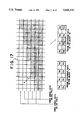
- FIG. 3 illustrates a positional relation of an enlarged boundary of an oblique line depicted on the lower left portion to the upper right portion of the picture and an input block (broken line) of the Hadamard transformation circuit.
- the lower portion of FIG. 3 illustrates a distribution of the field differences in the input block.
- the field difference data is supplied to the input block every other data as shown in FIG. 16.
- the field difference is obtained by subtracting the second field from the first field.
- the video signal is substantially canceled and only noise is obtained.
- the hatched portion of the field difference noise and the difference of the video signals in the boundary of oblique line are obtained.
- deterioration of an oblique line having an inclination as shown in FIG. 3 is most remarkable and accordingly description is made of an oblique line having inclination as shown in FIG. 3.
- Data to be processed currently is assumed to be data in the location expressed by x 11 .
- Deterioration of the oblique line is caused by feeding back the video signal contained in the field difference in the location where the boundary of oblique line exists as described above. Accordingly, it is considered that deterioration of the boundary of oblique line can be prevented by reducing to a small value outputs value of the nonlinear processing means 22 to reduce the feedback amount when a hatched portion comes in the location expressed by x 11 .
- FIG. 3 illustrates such an actual example.
- FIG. 4 is a schematic diagram showing a relation of the input block and the transformation equation. Marks of "+” and “-” shown in FIG. 4 represent "+1" and "-1", respectively, and the blank represents "0". These represent coefficients to be multiplied by data existing in the respective positions in the input block upon transformation. For example, F 00 is given by
- coefficients in positions of x 01 , x 03 , x 11 and x 13 are "-1".
- the difference of the video signal is dominant in the operation using data in the input block.
- F 00 the differences of the video signals appearing in two positions indicated by x 11 and x 12 are added and are increased to about twice.
- a value of F 00 may be considered about twice as large as the difference of the video signal.
- F 01 the differences of the video signals in two positions cancel each other and almost only noise is taken out from F 01 .
- components from which large values are obtained are F 00 , F 03 , F 10 and F 13 .
- FIG. 5 illustrates an input pattern obtained by moving the input pattern of FIG. 3 by two data blocks to the right and this is a case where the oblique line detection process is required in the same manner as in FIG. 3.
- the hatched portion of the field difference signal contains the difference of the video signals.
- the field difference signal is Hadamard-transformed by the block patterns of FIG. 4, it is considered that values of F 00 , F 02 , F 10 and F 12 are increased, and F 00 and F 10 , and F 02 and F 12 have a relation of different sign from each other.
- FIG. 6 illustrates an input pattern obtained by moving the input pattern of FIG. 5 by two data blocks to the right.
- the Hadamard transformation components have increased absolute values of F 00 , F 03 , F 11 and F 12 .
- the location shown by x 11 is not hatched (the video signal is not almost contained) and deterioration of the oblique line is not influenced even if feedback is made. Accordingly, in this case, detection of the oblique line is not made and this input pattern is excepted from objects to be detected in order to improve the S/N by increasing the feedback amount.
- FIG. 7 illustrates an input pattern obtained by moving the input pattern of FIG. 6 by two data blocks to the right
- FIG. 8 also illustrates an input pattern obtained by moving the input pattern of FIG. 7 by two data blocks to the right.
- absolute values of F 00 , F 02 , F 10 and F 12 are increased, and F 00 and F 10 , and F 02 and F 12 have a relation of the same sign.
- absolute values of F 00 , F 03 , F 10 and F 13 are increased, and F 00 and F 10 , and F 03 and F 13 have a relation of the same sign.
- the location shown by x 11 is not hatched and deterioration of the oblique line is not influenced even if feedback is made. Accordingly, in these cases, detection of the oblique line is not made and the input pattern is excepted from objects to be detected in order to improve the S/N by increasing the feedback amount.
- Absolute values of F 00 , F 02 , F 10 and F 12 are increased, and F 00 and F 10 , and F 02 and F 12 have a relation of different signs.
- Absolute values of F 00 , F 03 , F 10 and F 13 are increased, and F 00 and F 10 , and F 03 and F 13 have a relation of different signs.
- FIG. 9 illustrates horizontal lines depicted from the left portion to the right portion of the picture and the field difference, in which only noise is obtained in the blank portion of the field difference and both noise and a difference of the video signals are obtained in the hatched portion.
- the field difference signal of FIG. 9 is Hadamard-transformed by the eight patterns shown in FIG. 4, the absolute values of F 00 and F 10 are increased.
- numeral 31 denotes an absolute value circuit for obtaining an absolute value of an input signal
- 32 a register for holding a numerical value
- 33 a magnitude comparison circuit for comparing magnitudes of two input data
- 34, 35 and 36 logic circuits in which 34 is an XOR (exclusive OR) gate, 35 is an AND gate and 36 is an 0R gate.
- F 02 and F 03 inputted to the oblique line detection circuit are supplied to the absolute value circuits 31 in which absolute values thereof are obtained.
- An output signal of the absolute value circuit 31 is compared with a threshold value held in the register 32 in the magnitude comparison circuit 33 and only when the output signal of the absolute value circuit 31 is larger than the threshold value, the comparison circuit produces an "H" (high level) output signal.
- the MSBs (Most Significant Bits) of F 02 and F 12 and the MSBs of F 03 and F 13 are supplied to the respective XOR gates 34 and only when two input signals are different, each of the XOR gates 34 produces an "H” output signal.
- the AND gate 35 produces an "H" output
- the OR gate 36 produces an "H" output signal when the output signal of at least one of the AND gates 35 is "H". Accordingly, the oblique line detection condition is satisfied when the absolute values of F 02 and F 12 are larger than the threshold value and they have a relation of opposite signs, or when the absolute values of F 03 and F 13 are larger than the threshold value and they have a relation of opposite signs.
- FIG. 11 is a block diagram of a noise reduction apparatus according to the second embodiment of the present invention.
- elements designated by numerals 1, 2, 3, 6, 7, 10, 11, 21 and 23 are the same as those of FIG. 1 and have the same function.
- Numeral 9 denotes an Hadamard inverse transformation circuit, 41 a nonlinear processing circuit A, 42 a nonlinear processing circuit B, 43 a selection circuit for selecting one of output signals of the nonlinear processing circuits 41 and 42.
- the first subtraction means 6 calculates a difference of the input video signal and a one-field delayed video signal and an output of the first subtraction means 6 is supplied to the Hadamard transformation circuit 7.
- the Hadamard transformation circuit 7 divides the field difference into eight two-dimensional frequency components such as a low-frequency component, a vertical high-frequency component, a horizontal high-frequency component and the like.
- the two different nonlinear circuits 41 and 42 take out noise from the frequency components. More particularly, the nonlinear circuit 41 has an input/output characteristic of FIG. 12A and the nonlinear circuit 42 has an input/output characteristic of FIG. 12B.
- x in FIG. 12A and y in FIG. 12B have a relation of y ⁇ x.
- the characteristic of the nonlinear circuit shown in FIG. 12A is to obtain an improved large S/N and the characteristic shown in FIG. 12B is to reduce the feedback rate in the boundary of an oblique line in which deterioration in a static image tends to be striking.
- output signals F 02 , F 03 , F 12 and F 13 of the Hadamard transformation circuit 7 are supplied to the oblique line detection circuit 21, which judges whether the boundary of oblique line is contained in the input block of the Hadamard transformation circuit 7 or not from the four components. Operation and its principle of the oblique line detection circuit 21 are the same as described in the first embodiment and the circuit 21 produces a detection signal when the circuit detects the oblique line.
- the selection circuit 43 responds to a detection output signal of the oblique line detection circuit 21 and selects the output signal of the nonlinear processing circuit 42 when the oblique line is detected, otherwise the selection circuit selects the nonlinear processing circuit 41. In this manner, the existence of the boundary of an oblique line is detected and the feedback rate in the detected location is reduced to thereby suppress deterioration of the output image.
- the output signal of the selection circuit 43 is supplied to the Hadamard inverse transformation circuit 9 to be returned to noise in the time domain.
- the subtraction circuit 3 subtracts the noise from the input signal to thereby obtain the video signal having reduced noise.
- FIG. 13 is a block diagram of a noise reduction apparatus according to the third embodiment of the present invention.
- elements designated by numerals 1, 2, 3, 6, 7, 9, 10, 11, 21 and 23 are the same as those of FIG. 11 and have the same function.
- Numeral 51 denotes a nonlinear circuit capable of changing the nonlinear processing characteristic and an example of a circuit configuration thereof is shown in FIG. 14.
- numeral 61 denotes an input terminal for inputting components
- 62 an input terminal for inputting a detection result of an oblique line
- 63 an absolute value circuit for obtaining an absolute value of the input signal
- 64 a magnitude comparison circuit for comparing magnitudes of two input data
- 65 a register for holding a set value
- 66 and 67 selection circuits and 68 an output terminal.
- the nonlinear circuit 51 takes out noise from eight two-dimensional frequency components obtained in the Hadamard transformation circuit 7. More particularly, the nonlinear circuit 51 can attain two input/output characteristics of FIGS. 15A and 15B.
- the nonlinear circuit 51 having the characteristics shown in FIG. 15A is to obtain the improved large S/N and the nonlinear circuit having the characteristics shown in FIG. 15B is to reduce the feedback rate in the boundary of oblique line in which deterioration in a static image tends to be striking.
- output signals F 02 , F 03 , F 12 and F 13 of the Hadamard transformation circuit are supplied to the oblique line detection circuit 21, which judges whether the boundary of an oblique line is contained in the input block of the Hadamard transformation circuit 7 or not from the four components.
- the oblique line detection circuit 21 produces a detection signal when the circuit detects the oblique line.
- the nonlinear circuit 51 responds to an output signal of the oblique line detection circuit 21 and selects the process of FIG. 15B when the oblique line is detected, otherwise the circuit selects the process of FIG. 15A.
- the nonlinear processing circuit changes its nonlinear processing characteristics and the feedback rate in the detected location is controlled to be small to thereby suppress deterioration of the image quality.
- the output signal of the nonlinear circuit 51 is supplied to the Hadamard inverse transformation circuit 9 to be returned to noise in the time domain and is supplied to the subtraction circuit 3.
- the subtraction circuit 3 subtracts the noise from the input signal to thereby obtain the video signal having reduced noise.
- FIG. 14 schematically illustrates an example of an actual circuit configuration of the nonlinear circuit 51.
- the register 65 holds a value of z of FIGS. 15A and 15B.
- the selector circuit 66 outputs a ground level (that is, 0 level) when the oblique line detection result is "H", otherwise it outputs an output signal of the selector circuit 69.
- the selector circuit 69 outputs a value held in the register 65 when an input signal given to the input terminal 61 is positive or zero, that is, a most significant bit (MSB) of the input signal is "L", otherwise it outputs a value obtained by the NOT gate 70 and the adder 71 which increases a value of an output signal of the NOT gate by 1 so as to produce a signal having the same absolute value as the value held in the register 65 and a different sign from it.
- MSB most significant bit
- the comparator 64 Only when the output of the absolute value circuit 63 is larger than the value of the register, the comparator 64 produces an "H" output signal.
- the selector circuit 67 selects an output value of the selector circuit 66 when the output of the comparator 64 is "H", otherwise it produces the inputted component as it is.
- the nonlinear circuit 51 can perform the two nonlinear processes shown in FIG. 15 only by holding the value by the register and obtaining the result of the oblique line detection circuit.
- one nonlinear circuit is used to perform the two nonlinear processes, so that the circuit configuration is simplified. Since the two nonlinear processes are performed by one circuit configuration it is impossible to attain quite different nonlinear processes but it is sufficient to attain the object of the noise reduction apparatus.
- a noise reduction apparatus in which the existence of the boundary of an oblique line is detected from the components obtained by the Hadamard transformation and the nonlinear processing characteristics are changed by the detected result, so that deterioration of the image quality can be suppressed by reduction of the feedback rate in the boundary of an oblique line in which deterioration tends to be striking and the S/N can be improved by increase of the feedback rate in other locations to thereby attain excellent effect in improvement of the S/N as compared with the conventional field recursive type noise reduction apparatus.
Abstract
Description
F.sub.24 =H.sub.2 ·X.sub.24 ·H.sub.4
F.sub.00 =x.sub.00 +x.sub.01 +x.sub.02 +x.sub.03 +x.sub.10 +x.sub.11 +x.sub.12 +x.sub.13
F.sub.01 =x.sub.00 -x.sub.01 +x.sub.02 -x.sub.03 +x.sub.10 -x.sub.11 +X.sub.12 -x.sub.13
Claims (12)
Applications Claiming Priority (2)
| Application Number | Priority Date | Filing Date | Title |
|---|---|---|---|
| JP4167183A JP3006290B2 (en) | 1992-06-25 | 1992-06-25 | Noise reduction device |
| JP4-167183 | 1992-06-25 |
Publications (1)
| Publication Number | Publication Date |
|---|---|
| US5425114A true US5425114A (en) | 1995-06-13 |
Family
ID=15844970
Family Applications (1)
| Application Number | Title | Priority Date | Filing Date |
|---|---|---|---|
| US08/079,384 Expired - Lifetime US5425114A (en) | 1992-06-25 | 1993-06-21 | Noise reduction apparatus |
Country Status (4)
| Country | Link |
|---|---|
| US (1) | US5425114A (en) |
| EP (1) | EP0575995B1 (en) |
| JP (1) | JP3006290B2 (en) |
| DE (1) | DE69316938T2 (en) |
Cited By (8)
| Publication number | Priority date | Publication date | Assignee | Title |
|---|---|---|---|---|
| US6195132B1 (en) * | 1998-07-02 | 2001-02-27 | Hitachi, Ltd. | Noise reduction signal processing circuit and display apparatus |
| US6285411B1 (en) * | 1997-10-10 | 2001-09-04 | Philips Electronics North America Corporation | Circuit for video moiré reduction |
| US20020080283A1 (en) * | 2000-05-17 | 2002-06-27 | Marko Hahn | Method and apparatus for measuring the noise contained in a picture |
| US20050058348A1 (en) * | 2003-08-06 | 2005-03-17 | Sony Corporation | Edge detecting apparatus, noise eliminating apparatus, edge detecting method, and noise eliminating method and program |
| US20070247554A1 (en) * | 2006-04-18 | 2007-10-25 | Pioneer Corporation | Noise reduction apparatus of frame recursive type |
| US20090265529A1 (en) * | 2008-04-16 | 2009-10-22 | Nec Corporation | Processor apparatus and method of processing multiple data by single instructions |
| US20100177128A1 (en) * | 2004-06-10 | 2010-07-15 | Jun Someya | Liquid-crystal-driving image processing circuit, liquid-crystal-driving image processing method, and liquid crystal display apparatus |
| US20130236095A1 (en) * | 2012-03-08 | 2013-09-12 | Sony Corporation | Image processing device, image processing method, and program |
Citations (6)
| Publication number | Priority date | Publication date | Assignee | Title |
|---|---|---|---|---|
| US4242705A (en) * | 1978-09-21 | 1980-12-30 | Sony Corporation | Noise reduction system for video signals |
| US4860104A (en) * | 1987-10-26 | 1989-08-22 | Pioneer Electronic Corporation | Noise eliminating apparatus of a video signal utilizing a recursive filter having spatial low pass and high pass filters |
| US4901150A (en) * | 1988-11-22 | 1990-02-13 | Sony Corporation | Automatic noise reduction for individual frequency components of a signal |
| JPH044676A (en) * | 1990-04-23 | 1992-01-09 | Matsushita Electric Ind Co Ltd | Noise reduction device |
| EP0504428A1 (en) * | 1990-10-05 | 1992-09-23 | Matsushita Electric Industrial Co., Ltd. | Noise reducing apparatus |
| US5247354A (en) * | 1990-04-23 | 1993-09-21 | Matsushita Electric Industrial Co., Ltd. | Noise reducing apparatus for reducing noise in moving video image signals |
-
1992
- 1992-06-25 JP JP4167183A patent/JP3006290B2/en not_active Expired - Fee Related
-
1993
- 1993-06-21 US US08/079,384 patent/US5425114A/en not_active Expired - Lifetime
- 1993-06-23 DE DE69316938T patent/DE69316938T2/en not_active Expired - Fee Related
- 1993-06-23 EP EP93110048A patent/EP0575995B1/en not_active Expired - Lifetime
Patent Citations (6)
| Publication number | Priority date | Publication date | Assignee | Title |
|---|---|---|---|---|
| US4242705A (en) * | 1978-09-21 | 1980-12-30 | Sony Corporation | Noise reduction system for video signals |
| US4860104A (en) * | 1987-10-26 | 1989-08-22 | Pioneer Electronic Corporation | Noise eliminating apparatus of a video signal utilizing a recursive filter having spatial low pass and high pass filters |
| US4901150A (en) * | 1988-11-22 | 1990-02-13 | Sony Corporation | Automatic noise reduction for individual frequency components of a signal |
| JPH044676A (en) * | 1990-04-23 | 1992-01-09 | Matsushita Electric Ind Co Ltd | Noise reduction device |
| US5247354A (en) * | 1990-04-23 | 1993-09-21 | Matsushita Electric Industrial Co., Ltd. | Noise reducing apparatus for reducing noise in moving video image signals |
| EP0504428A1 (en) * | 1990-10-05 | 1992-09-23 | Matsushita Electric Industrial Co., Ltd. | Noise reducing apparatus |
Non-Patent Citations (2)
| Title |
|---|
| Patent Abstracts of Japan, vol. 16, No. 150 (E 1189) 14 Apr. 1992 & JP A 04 004 676 (Matsushita Electric Industrial Co., Ltd.) 9 Jan. 1992. * |
| Patent Abstracts of Japan, vol. 16, No. 150 (E-1189) 14 Apr. 1992 & JP-A-04 004 676 (Matsushita Electric Industrial Co., Ltd.) 9 Jan. 1992. |
Cited By (12)
| Publication number | Priority date | Publication date | Assignee | Title |
|---|---|---|---|---|
| US6285411B1 (en) * | 1997-10-10 | 2001-09-04 | Philips Electronics North America Corporation | Circuit for video moiré reduction |
| US6195132B1 (en) * | 1998-07-02 | 2001-02-27 | Hitachi, Ltd. | Noise reduction signal processing circuit and display apparatus |
| US20020080283A1 (en) * | 2000-05-17 | 2002-06-27 | Marko Hahn | Method and apparatus for measuring the noise contained in a picture |
| US7064793B2 (en) * | 2000-05-17 | 2006-06-20 | Micronas Gmbh | Method and apparatus for measuring the noise contained in a picture |
| US20050058348A1 (en) * | 2003-08-06 | 2005-03-17 | Sony Corporation | Edge detecting apparatus, noise eliminating apparatus, edge detecting method, and noise eliminating method and program |
| US7457475B2 (en) * | 2003-08-06 | 2008-11-25 | Sony Corporation | Edge detecting apparatus, noise eliminating apparatus, edge detecting method, and noise eliminating method and program |
| US20100177128A1 (en) * | 2004-06-10 | 2010-07-15 | Jun Someya | Liquid-crystal-driving image processing circuit, liquid-crystal-driving image processing method, and liquid crystal display apparatus |
| US8150203B2 (en) * | 2004-06-10 | 2012-04-03 | Mitsubishi Electric Corporation | Liquid-crystal-driving image processing circuit, liquid-crystal-driving image processing method, and liquid crystal display apparatus |
| US20070247554A1 (en) * | 2006-04-18 | 2007-10-25 | Pioneer Corporation | Noise reduction apparatus of frame recursive type |
| US20090265529A1 (en) * | 2008-04-16 | 2009-10-22 | Nec Corporation | Processor apparatus and method of processing multiple data by single instructions |
| US8041927B2 (en) * | 2008-04-16 | 2011-10-18 | Nec Corporation | Processor apparatus and method of processing multiple data by single instructions |
| US20130236095A1 (en) * | 2012-03-08 | 2013-09-12 | Sony Corporation | Image processing device, image processing method, and program |
Also Published As
| Publication number | Publication date |
|---|---|
| EP0575995A2 (en) | 1993-12-29 |
| DE69316938T2 (en) | 1998-08-27 |
| EP0575995B1 (en) | 1998-02-11 |
| DE69316938D1 (en) | 1998-03-19 |
| JPH0614218A (en) | 1994-01-21 |
| JP3006290B2 (en) | 2000-02-07 |
| EP0575995A3 (en) | 1994-07-20 |
Similar Documents
| Publication | Publication Date | Title |
|---|---|---|
| US7245326B2 (en) | Method of edge based interpolation | |
| EP0731601B1 (en) | Video signal noise reduction apparatus | |
| EP1313310A2 (en) | Method of low latency interlace to progressive video format conversion | |
| JP4169188B2 (en) | Image processing method | |
| US4500911A (en) | Noise reduction apparatus | |
| KR20070094796A (en) | Spatio-temporal adaptive video de-interlacing | |
| US5546135A (en) | Contour restoration apparatus | |
| US5425114A (en) | Noise reduction apparatus | |
| KR100949403B1 (en) | Image noise reduction method and apparatus | |
| US5539541A (en) | Image processing apparatus including noise elimination circuits | |
| JP2002077623A (en) | Image processing apparatus | |
| KR100281877B1 (en) | Impulse noise reduction apparatus and method | |
| US5635990A (en) | Apparatus for cancelling noise and improving details of images | |
| US7075588B2 (en) | Edge correction method and apparatus | |
| CN101141655A (en) | Video signal picture element point chromatic value regulation means | |
| US20040008902A1 (en) | Image noise reduction method and device | |
| US6259480B1 (en) | Sequential scanning converter | |
| US7336320B2 (en) | Method and apparatus for temporally recursive chrominance signal noise reduction | |
| JPH10262160A (en) | Signal-to-noise ratio (s/n)detector and noise reduction device | |
| WO2001097510A1 (en) | Image processing system, image processing method, program, and recording medium | |
| US8212920B2 (en) | Apparatus and method of motion adaptive image processing | |
| US7012719B1 (en) | Sign sensitive aperture correction system and method | |
| US10264212B1 (en) | Low-complexity deinterlacing with motion detection and overlay compensation | |
| JPH0944648A (en) | Image processing device and method therefor | |
| JP3022977B2 (en) | Television signal interpolation method |
Legal Events
| Date | Code | Title | Description |
|---|---|---|---|
| AS | Assignment |
Owner name: MATSUSHITA ELECTRIC INDUSTRIAL CO., LTD., JAPAN Free format text: ASSIGNMENT OF ASSIGNORS INTEREST;ASSIGNORS:HAMASAKI, TAKESHI;YASHITA, YUKIKO;REEL/FRAME:006614/0977 Effective date: 19930617 |
|
| STPP | Information on status: patent application and granting procedure in general |
Free format text: APPLICATION UNDERGOING PREEXAM PROCESSING |
|
| FEPP | Fee payment procedure |
Free format text: PAYOR NUMBER ASSIGNED (ORIGINAL EVENT CODE: ASPN); ENTITY STATUS OF PATENT OWNER: LARGE ENTITY |
|
| FPAY | Fee payment |
Year of fee payment: 4 |
|
| REMI | Maintenance fee reminder mailed | ||
| FPAY | Fee payment |
Year of fee payment: 8 |
|
| SULP | Surcharge for late payment |
Year of fee payment: 7 |
|
| AS | Assignment |
Owner name: BMO CAPITAL CORPORATION, ONTARIO Free format text: SECURITY INTEREST;ASSIGNOR:NORTH AMERICAN POOL COMPANY;REEL/FRAME:014428/0341 Effective date: 20021211 |
|
| FPAY | Fee payment |
Year of fee payment: 12 |