US20110316632A1 - Optical communication device - Google Patents
Optical communication device Download PDFInfo
- Publication number
- US20110316632A1 US20110316632A1 US13/201,212 US200913201212A US2011316632A1 US 20110316632 A1 US20110316632 A1 US 20110316632A1 US 200913201212 A US200913201212 A US 200913201212A US 2011316632 A1 US2011316632 A1 US 2011316632A1
- Authority
- US
- United States
- Prior art keywords
- circuit
- amplifier circuit
- signal
- level
- communication device
- Prior art date
- Legal status (The legal status is an assumption and is not a legal conclusion. Google has not performed a legal analysis and makes no representation as to the accuracy of the status listed.)
- Granted
Links
- 230000003287 optical effect Effects 0.000 title claims abstract description 80
- 238000004891 communication Methods 0.000 title claims abstract description 79
- 238000012937 correction Methods 0.000 claims description 12
- 238000001914 filtration Methods 0.000 claims 1
- 101710170230 Antimicrobial peptide 1 Proteins 0.000 abstract description 78
- 238000010586 diagram Methods 0.000 description 46
- 230000003247 decreasing effect Effects 0.000 description 12
- 230000001965 increasing effect Effects 0.000 description 10
- 238000000034 method Methods 0.000 description 10
- 230000003071 parasitic effect Effects 0.000 description 10
- 101710170231 Antimicrobial peptide 2 Proteins 0.000 description 8
- 230000003321 amplification Effects 0.000 description 8
- 238000003199 nucleic acid amplification method Methods 0.000 description 8
- 230000000694 effects Effects 0.000 description 6
- 230000008569 process Effects 0.000 description 6
- 239000004065 semiconductor Substances 0.000 description 5
- HODRFAVLXIFVTR-RKDXNWHRSA-N tevenel Chemical compound NS(=O)(=O)C1=CC=C([C@@H](O)[C@@H](CO)NC(=O)C(Cl)Cl)C=C1 HODRFAVLXIFVTR-RKDXNWHRSA-N 0.000 description 5
- 230000006872 improvement Effects 0.000 description 3
- 230000004048 modification Effects 0.000 description 2
- 238000012986 modification Methods 0.000 description 2
- 239000000758 substrate Substances 0.000 description 2
- 101000870046 Sus scrofa Glutamate dehydrogenase 1, mitochondrial Proteins 0.000 description 1
- 230000004075 alteration Effects 0.000 description 1
- 230000015572 biosynthetic process Effects 0.000 description 1
- 230000000295 complement effect Effects 0.000 description 1
- 238000013461 design Methods 0.000 description 1
- 230000002708 enhancing effect Effects 0.000 description 1
- 230000005669 field effect Effects 0.000 description 1
- 239000012212 insulator Substances 0.000 description 1
- 239000002184 metal Substances 0.000 description 1
- 229910044991 metal oxide Inorganic materials 0.000 description 1
- 150000004706 metal oxides Chemical class 0.000 description 1
- 229910021421 monocrystalline silicon Inorganic materials 0.000 description 1
- 230000010355 oscillation Effects 0.000 description 1
- 238000011084 recovery Methods 0.000 description 1
- 230000003252 repetitive effect Effects 0.000 description 1
- 230000035945 sensitivity Effects 0.000 description 1
Images


Classifications
-
- H—ELECTRICITY
- H03—ELECTRONIC CIRCUITRY
- H03F—AMPLIFIERS
- H03F3/00—Amplifiers with only discharge tubes or only semiconductor devices as amplifying elements
- H03F3/04—Amplifiers with only discharge tubes or only semiconductor devices as amplifying elements with semiconductor devices only
- H03F3/08—Amplifiers with only discharge tubes or only semiconductor devices as amplifying elements with semiconductor devices only controlled by light
- H03F3/087—Amplifiers with only discharge tubes or only semiconductor devices as amplifying elements with semiconductor devices only controlled by light with IC amplifier blocks
-
- H—ELECTRICITY
- H03—ELECTRONIC CIRCUITRY
- H03F—AMPLIFIERS
- H03F1/00—Details of amplifiers with only discharge tubes, only semiconductor devices or only unspecified devices as amplifying elements
- H03F1/08—Modifications of amplifiers to reduce detrimental influences of internal impedances of amplifying elements
- H03F1/22—Modifications of amplifiers to reduce detrimental influences of internal impedances of amplifying elements by use of cascode coupling, i.e. earthed cathode or emitter stage followed by earthed grid or base stage respectively
- H03F1/223—Modifications of amplifiers to reduce detrimental influences of internal impedances of amplifying elements by use of cascode coupling, i.e. earthed cathode or emitter stage followed by earthed grid or base stage respectively with MOSFET's
-
- H—ELECTRICITY
- H03—ELECTRONIC CIRCUITRY
- H03F—AMPLIFIERS
- H03F1/00—Details of amplifiers with only discharge tubes, only semiconductor devices or only unspecified devices as amplifying elements
- H03F1/34—Negative-feedback-circuit arrangements with or without positive feedback
-
- H—ELECTRICITY
- H03—ELECTRONIC CIRCUITRY
- H03F—AMPLIFIERS
- H03F3/00—Amplifiers with only discharge tubes or only semiconductor devices as amplifying elements
- H03F3/04—Amplifiers with only discharge tubes or only semiconductor devices as amplifying elements with semiconductor devices only
- H03F3/08—Amplifiers with only discharge tubes or only semiconductor devices as amplifying elements with semiconductor devices only controlled by light
- H03F3/082—Amplifiers with only discharge tubes or only semiconductor devices as amplifying elements with semiconductor devices only controlled by light with FET's
-
- H—ELECTRICITY
- H03—ELECTRONIC CIRCUITRY
- H03F—AMPLIFIERS
- H03F3/00—Amplifiers with only discharge tubes or only semiconductor devices as amplifying elements
- H03F3/30—Single-ended push-pull [SEPP] amplifiers; Phase-splitters therefor
- H03F3/3001—Single-ended push-pull [SEPP] amplifiers; Phase-splitters therefor with field-effect transistors
- H03F3/3022—CMOS common source output SEPP amplifiers
-
- H—ELECTRICITY
- H03—ELECTRONIC CIRCUITRY
- H03F—AMPLIFIERS
- H03F3/00—Amplifiers with only discharge tubes or only semiconductor devices as amplifying elements
- H03F3/50—Amplifiers in which input is applied to, or output is derived from, an impedance common to input and output circuits of the amplifying element, e.g. cathode follower
- H03F3/505—Amplifiers in which input is applied to, or output is derived from, an impedance common to input and output circuits of the amplifying element, e.g. cathode follower with field-effect devices
-
- H—ELECTRICITY
- H04—ELECTRIC COMMUNICATION TECHNIQUE
- H04B—TRANSMISSION
- H04B10/00—Transmission systems employing electromagnetic waves other than radio-waves, e.g. infrared, visible or ultraviolet light, or employing corpuscular radiation, e.g. quantum communication
- H04B10/60—Receivers
- H04B10/66—Non-coherent receivers, e.g. using direct detection
- H04B10/69—Electrical arrangements in the receiver
- H04B10/693—Arrangements for optimizing the preamplifier in the receiver
- H04B10/6933—Offset control of the differential preamplifier
-
- H—ELECTRICITY
- H03—ELECTRONIC CIRCUITRY
- H03F—AMPLIFIERS
- H03F2200/00—Indexing scheme relating to amplifiers
- H03F2200/453—Controlling being realised by adding a replica circuit or by using one among multiple identical circuits as a replica circuit
Definitions
- the present invention relates to an optical communication device, and more particularly, the present invention relates to a technique effectively applied to an optical communication device including a transimpedance amplifier (TIA).
- TIA transimpedance amplifier
- each of FIGS. 4 and 5 of Non-Patent Document 1 shows an amplifier circuit and a TIA having a negative feedback configuration including a feedback resistance between an input and an output of this amplifier circuit.
- this amplifier circuit is configured by three stages formed of a grounded-gate amplifier stage, a grounded-source amplifier stage, and a source follower stage.
- FIG. 4 shows a method of setting a circuit parameter for decreasing noise in the grounded-gate amplifier stage
- FIG. 5 shows a system of enhancing a bandwidth by using an inductance for a load element of the grounded-gate amplifier stage or the grounded-source amplifier stage.
- FIG. 2 of Non-Patent Document 2 shows a TIA having an open-loop configuration.
- This TIA has a configuration including amplifier stages formed of a grounded-gate amplifier stage in an initial stage and a grounded-source amplifier stage and the grounded-gate amplifier stage in a latter stage, in which the grounded-gate amplifier stage in the latter stage is gain-boosted by the grounded-source amplifier stage.
- Each MOS transistor is formed so as to have a large gate width, so that its bandwidth is improved.
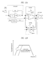
- FIG. 16 is a schematic diagram showing a configuration example of an optical communication device studied as an assumption of the present invention.
- the optical communication device shown in FIG. 16 is configured by: a pre-amplifier circuit PREAMP_C for amplifying a current signal from a photodiode PD which is generated by an optical input and converting the current signal into a voltage signal; a post-amplifier circuit PSAMP for amplifying an output of the pre-amplifier circuit; and a limit amplifier circuit LMTAMP for further amplifying an output of the post-amplifier circuit.
- PREAMP_C for amplifying a current signal from a photodiode PD which is generated by an optical input and converting the current signal into a voltage signal
- PSAMP for amplifying an output of the pre-amplifier circuit
- LMTAMP limit amplifier circuit
- the PREAMP_C converts a current signal of several tens to several hundreds of ⁇ A into a voltage signal of about 10 mV
- the PSAMP receives the voltage signal and generates a voltage signal of 200 mV to 300 mV
- the LMTAMP receives the voltage signal and generates a voltage signal of about 500 mV.
- the LMTAMP is a circuit for amplifying the voltage signal up to a logic level of a latter-stage logic circuit (for example, CDR (Clock Data Recovery) circuit or others) not shown.
- a low noise characteristic in addition to a high gain characteristic (for example, about 50 dB) and a high speed performance is particularly important in the PREAMP_C.
- the PSAMP if it can obtain a sufficient input voltage signal through the PREAMP_C, it is required to put a priority on the high speed performance higher than the gain (for example, about 20 dB), the low noise characteristic, and others. For example, a bandwidth of about 4/3 times that of the PREAMP_C is preferred. Note that, in FIG.
- the PREAMP_C is an amplifier circuit having a single input/output
- the PSAMP is an amplifier circuit having a differential input/output
- a voltage reference generator circuit VREFG for generating a reference voltage is provided at one end of the PSAMP.
- the VREFG can be achieved by, for example, detecting a DC component by a low pass filter for the output of the PREAMP_C or others. However, in this case, there is a concern of area increase.
- FIGS. 17A to 17C are explanatory diagrams each showing a detail of the pre-amplifier circuit PREAMP_C in FIG. 16 .
- the PREAMP_C is a negative feedback circuit including: an amplifier circuit AMP_C with a negative gain (G); and a feedback resistance Rf connected between an input and an output of the amplifier circuit.
- G negative gain
- Rf feedback resistance
- G in order to increase the gain (G), it can be considered to, for example, provide a plurality of amplifier stages (grounded-gate amplifier stage and grounded-source amplifier stage) as disclosed in Non-Patent Document 1.
- an amount of the noise is generally increased by increasing the number of amplifier stages.
- the initial stage is the grounded-gate amplifier stage, although there is a merit that an input impedance can be decreased, a sensitivity to the noise is particularly increased.
- FIG. 17C shows a characteristic example of an input voltage Vi and an output voltage Vo of the AMP_C, and the high gain means that its slope (Vo/Vi) is steep.
- the gain is significantly changed, and therefore, there is a concern of not obtaining a predetermined performance.
- Non-Patent Document 2 when, for example, the amplifier circuit having the open-loop configuration disclosed in Non-Patent Document 2 is used, a low input impedance (resulting in the improvement of the bandwidth) can be achieved by the grounded-gate stage in the initial stage despite a noise problem, and the improvement of the gain (also contributing to the improvement of the bandwidth) can be achieved by the amplifier stage in the latter stage.
- each MOS transistor is configured by a large gate width, and therefore, there is a concern of limitation of the bandwidth due to a parasitic capacitance inside a circuit.
- the present invention has been made in consideration of such a problem, and one of a preferred aims of the invention is to provide an optical communication device which can be operated at high speed.
- the above and other preferred aims and novel characteristics of the present invention will be apparent from the description of the present specification and the accompanying drawings.
- An optical communication device includes: a pre-amplifier circuit for amplifying a current signal from a photodiode and converting it into a voltage signal; and an operating-point controller circuit for controlling the pre-amplifier circuit.
- the pre-amplifier circuit has a negative feedback configuration including a feedback path including: an amplification path; and a feedback resistance.
- the amplification path includes: a first level-shift circuit; and a first amplifier circuit connected to a latter stage of the first level-shift circuit.
- the first level-shift circuit performs a level-shift operation in accordance with a first control signal from the operating-point controller circuit.
- the operating-point controller circuit includes a replica circuit which is configured by the same circuit and circuit parameter as those of the first amplifier circuit, and besides, whose input and output are electrically connected to each other, and generates the first control signal so that a direct-current voltage level of an output signal from the replica circuit is matched with a direct-current voltage level of an input signal of the first amplifier circuit.
- a logical threshold voltage obtained from the output of the replica circuit can be set as the operating point of the first amplifier circuit, and, by this setting, the first amplifier circuit can be stably operated at a high gain.
- a high frequency bandwidth of the pre-amplifier circuit having the negative feedback configuration is enhanced, so that the high speed performance of the optical communication device can be achieved.
- the operating-point controller circuit includes, for example: a first current source for generating the same direct current as a direct current level of a current signal from a photodiode; a replica pre-amplifier circuit; and a second amplifier circuit.
- the replica pre-amplifier circuit is configured by the same circuit and circuit parameter as those of the pre-amplifier circuit, and performs an amplification operation with taking the direct current from the first current source as its input.
- the second amplifier circuit performs a differential amplification between an input signal of the first amplifier circuit in the replica pre-amplifier circuit and an output signal of the replica circuit, and outputs the first control signal.
- each first level-shift circuit in the pre-amplifier circuit and the replica pre-amplifier circuit receives the first control signal, and performs the level-shift operation.
- the output of the replica pre-amplifier circuit can be also used as a reference signal of a post-amplifier circuit which is generally provided in the latter stage of the pre-amplifier circuit. That is, the post-amplifier circuit performs a differential amplification for the output signal from the pre-amplifier circuit with taking this reference signal as a reference.
- a circuit for example, a low pass filter
- a voltage level of this reference signal becomes an optimum value (center of output voltage magnitude of the pre-amplifier circuit), and therefore, the high speed performance of the post-amplifier circuit can be also achieved.
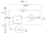
- FIG. 1 is a block diagram showing a configuration example of a principal unit in an optical communication device according to a first embodiment of the present invention
- FIG. 2 is a block diagram showing a configuration example of an operating-point controller circuit in the optical communication device of FIG. 1 ;
- FIG. 3 is a circuit diagram showing a detailed configuration example in an optical communication device including configurations of FIGS. 1 and 2 ;
- FIGS. 4A to 4F are circuit diagrams each showing a detailed configuration example of an amplifier circuit in the pre-amplifier circuit of FIG. 1 ;
- FIG. 5 is a circuit diagram showing a configuration example of a principal unit in an optical communication device according to a second embodiment of the present invention.
- FIGS. 6A and 6B are a block diagram showing a configuration example of a principal unit in an optical communication device according to a third embodiment of the present invention, and a circuit diagram showing a detailed configuration example of a pre-amplifier circuit in FIG. 6A , respectively;
- FIG. 7 is a block diagram showing a configuration example of a principal unit in an optical communication device according to a fourth embodiment of the present invention.
- FIG. 8 is a circuit diagram showing a detailed configuration example of an amplifier circuit in the pre-amplifier circuit of FIG. 7 ;
- FIGS. 9A and 9B are a block diagram showing a configuration example of a principal unit in an optical communication device according to a fifth embodiment of the present invention, and a circuit diagram showing a detailed configuration example of a pre-amplifier circuit in FIG. 9A , respectively;
- FIG. 10 is a block diagram showing a configuration example of an optical communication device according to a sixth embodiment of the present invention.
- FIGS. 11A and 11B are a schematic diagram showing a configuration example of a post-amplifier circuit in the optical communication device of FIG. 10 , and an explanatory diagram showing an operation example of FIG. 11A , respectively;
- FIGS. 12A and 12B are a block diagram showing a configuration example of an optical communication device according to a seventh embodiment of the present invention, and an explanatory diagram showing an effect example of FIG. 12A , respectively;
- FIG. 13 is a block diagram showing a configuration example of an optical communication device according to an eighth embodiment of the present invention.
- FIGS. 14A and 14B are circuit diagrams each showing a detailed configuration example of a pre-amplifier circuit in the optical communication device of FIG. 13 ;
- FIG. 15 is a block diagram showing a configuration example of an optical communication device studied as a comparison object of FIG. 12 ;
- FIG. 16 is a schematic diagram showing a configuration example of an optical communication device studied as an assumption of the present invention.
- FIGS. 17A to 17C are explanatory diagrams each showing a detail of a pre-amplifier circuit in FIG. 16 .
- the invention will be described in a plurality of sections or embodiments when required as a matter of convenience. However, these sections or embodiments are not irrelevant to each other unless otherwise stated, and the one relates to the entire or a part of the other as a modification example, details, or a supplementary explanation thereof. Also, in the embodiments described below, when referring to the number of elements (including number of pieces, values, amount, range, and the like), the number of the elements is not limited to a specific number unless otherwise stated or except the case where the number is apparently limited to a specific number in principle. The number larger or smaller than the specified number is also applicable.
- the components are not always indispensable unless otherwise stated or except the case where the components are apparently indispensable in principle.
- the shape of the components, positional relation thereof, and the like are mentioned, the substantially approximate and similar shapes and the like are included therein unless otherwise stated or except the case where it is conceivable that they are apparently excluded in principle. The same goes for the numerical value and the range described above.
- a circuit element configuring each functional block of the embodiments is not particularly limited.
- the circuit element is formed on a semiconductor substrate such as monocrystalline silicon by an integrated circuit technique such as CMOS (complementary MOS transistor) which is publicly known.
- CMOS complementary MOS transistor
- MOS Metal Oxide Semiconductor
- MISFET Metal Insulator Semiconductor Field Effect Transistor
- a P-channel type MOS transistor PMOS transistor
- NMOS transistor N-channel type MOS transistor
- a connection of a substrate potential of the MOS transistor is not particularly mentioned. However, as long as the connection is within a scope that the MOS transistor can be normally operated, a method of the connection is not particularly limited.
- FIG. 1 is a block diagram showing a configuration example of a principal unit in an optical communication device according to a first embodiment of the present invention.
- An optical communication device shown in FIG. 1 is configured by: a pre-amplifier circuit PREAMP 1 which receives a current signal Iin from a photodiode PD generated by an optical input, and amplifies and converts the current signal into a voltage signal; and an operating-point controller circuit VTCTL 1 .
- the PREAMP 1 is applied instead of a pre-amplifier circuit PREAMP_C shown in FIG. 16 .
- the PREAMP 1 is a transimpedance amplifier (TIA) having a negative feedback configuration, and is configured by: a level-shift circuit LS 1 ; an amplifier circuit AMP 1 whose input is an output of the level-shift circuit and which has a negative gain; and a feedback resistance Rf 1 connected between an output of the AMP 1 and an input of the LS 1 .
- the current signal Iin from the PD is converted into a voltage signal via the Rf 1 , and voltage signals generated at one end of the Rf 1 and an output node Vout which is an output of the AMP 1 are expressed nearly as “Iin ⁇ Rf 1 ” when a gain of the AMP 1 is high.
- the AMP 1 is configured by one amplifier stage whose gain (output voltage signal Vo/input voltage signal Vi) is designed to an extremely large value. In this manner, as described in FIGS. 16 to 17C , the low noise characteristic and the high speed performance can be achieved. However, as shown in FIG. 17C , if the operating point of the AMP 1 is shifted due to process variation or others, a desired gain cannot be obtained, and therefore, there is a concern of preventing the high speed performance of the PREAMP 1 .
- the VTCTL 1 includes a replica circuit having the same circuit configuration and element parameter as those of the AMP 1 although their details will be described later, and an operating-point control signal Vcon for determining the operating point of the AMP 1 is generated by using this replica circuit.
- the LS 1 is typically configured by a source follower circuit which level-shifts a DC level contained in an extremely-minute voltage signal generated by the Iin in accordance with the Vcon, and outputs the level-shifted signal to the AMP 1 . In this manner, the operating point of the AMP 1 is determined to an optimal value through this level shift, and, as a result, the desired gain can be obtained in the AMP 1 , and besides, the high speed performance of the PREAMP 1 can be achieved.
- the LS 1 by configuring the LS 1 by a gate-input transistor such as the source follower circuit, the low noise characteristic can be achieved.
- the VTCTL 1 also generates a reference voltage Vref to be a DC component of an output signal in the output node Vout in addition to the Vcon although its detail will be described later.
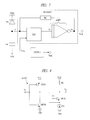
- FIG. 2 is a block diagram showing a configuration example of the operating-point controller circuit VTCTL 1 in the optical communication device of FIG. 1 .
- the operating-point controller circuit VTCTL 1 shown in FIG. 2 includes: a constant current source IS 1 to be a circuit reflecting the photodiode PD of FIG. 1 ; and a level-shift circuit LS 2 , an amplifier circuit AMP 1 a , and a feedback resistance Rf 1 a , to be a replica amplifier circuit reflecting the pre-amplifier circuit PREAMP 1 of FIG. 1 , and besides, includes: an amplifier circuit AMP 2 ; and a replica circuit REP.
- the AMP 1 a and the Rf 1 a are configured by the same circuit (also including the circuit parameter) as those of the AMP 1 and the Rf 1 in the PREAMP 1 of FIG. 1 .
- the IS 1 generates the same current as a DC current of the PD in FIG. 1 .
- the replica circuit REP includes: an amplifier circuit AMP 1 b to be the same circuit (also including the circuit parameter) as those of the AMP 1 of FIG. 1 and the AMP 1 a of FIG. 2 ; and a feedback resistance Rf 2 connected between an input and an output of the amplifier circuit.
- the Rf 2 is for preventing the oscillation of the AMP 1 b and electrically shorting between the input and the output of the AMP 1 b .
- the AMP 2 performs a differential amplifying operation with taking the output of this AMP 1 b as a ( ⁇ ) input and the output of the LS 2 (input of the AMP 1 a ) as a (+) input, and outputs the operating-point control signal Vcon.
- This Vcon is outputted to the LS 1 of the PREAMP 1 of FIG. 1 , and besides, is outputted to the LS 2 of FIG. 2 .
- the LS 2 is configured by the nearly same circuit (also including the circuit parameter) as those of the LS 1 of the PREAMP 1 of FIG. 1 , and level-shifts a DC voltage signal generated by the IS 1 based on the Vcon and outputs the level-shifted signal to the AMP 1 a and the AMP 2 .
- the AMP 2 has a sufficiently large gain, and generates the operating-point control signal Vcon to be a value such as matching an input voltage level to the AMP 1 a with a logical threshold level of an output from the AMP 1 a by the feedback via this LS 2 . And, this Vcon is supplied to the LS 1 in the PREAMP 1 of FIG.
- an input voltage signal Vi to the AMP 1 in the PREAMP 1 is also matched with a logical threshold level from the AMP 1 b of FIG. 2 . Therefore, the AMP 1 performs an amplifying operation with taking a logical threshold level with a high gain as the operating point, and therefore, the high speed performance of the PREAMP 1 can be achieved as described above.
- a difference point between the LS 2 of FIG. 2 and the LS 1 of FIG. 1 is that the LS 2 can correct a level-shift amount even by an operating-point correction signal Vc.
- the AMP 1 , the AMP 1 a , and the AMP 1 b are the same circuit as each other, and, when they are formed on the same semiconductor chip, they are normally affected by the same process variation, and therefore, the operating-point correction signal Vc is not always provided. However, for example, when a degree of the variation is different from each other, the correction can be also performed by the Vc. Also, the output of the AMP 1 a of FIG. 2 is used as the above-described reference voltage Vref.
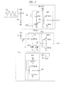
- FIG. 3 is a circuit diagram showing a detailed configuration example in an optical communication device including configurations of FIGS. 1 and 2 .
- the level-shift circuit LS 1 is a source follower circuit including: an NMOS transistor MN 20 ; and a variable current source ISV 1 connected to a source of the MN 20 .
- the photodiode PD and the feedback resistance Rf 1 are connected in parallel, and an output signal Vth is outputted from the source thereof.
- the ISV 1 its current value is controlled in accordance with the operating-point control signal Vcon, and the DC level of the Vth is controlled in accordance with the controlled current value.
- the amplifier circuit AMP 1 is configured by a CMOS inverter circuit including a PMOS transistor MP 10 and an NMOS transistor MN 10 , and is operated with taking the Vth from the LS 1 as an input.
- the output of the AMP 1 is connected to the output node Vout, and besides, is connected to a gate of the MN 20 via the feedback resistance Rf 1 .
- the level-shift circuit LS 2 is a source follower circuit including an NMOS transistor MN 20 a and two variable current sources ISV 1 a and ISV 2 connected to a source of the MN 20 a .
- the MN 20 a includes the same circuit parameter as that of the MN 20 , and a gate of the MN 20 a is connected in parallel to the constant current source IS 1 and the feedback resistance Rf 1 a , and a source thereof outputs an output signal Vth′.
- the IS 1 is set to a current value Ib of the DC level in the current signal Iin of the PD.
- the ISV 1 a includes the same circuit parameter as that of the ISV 1 , a current value of the ISV 1 a is controlled in accordance with the Vcon, and the DC level of the Vth′ is controlled in accordance with this controlled current value.
- a current value of the ISV 2 is controlled in accordance with the operating-point correction signal Vc, and the DC level of the Vth′ is finely adjusted.
- the amplifier circuit AMP 1 a is configured by a CMOS inverter circuit including a PMOS transistor MP 10 a and an NMOS transistor MN 10 a , and is configured by the same circuit parameter as that of the CMOS inverter circuit of the AMP 1 .
- the AMP 1 a is operated with taking the Vth′ from the LS 2 as its input to input the reference voltage Vref which is its output to a gate of the MN 20 a via the feedback resistance Rf 1 a .
- the replica circuit REP is configured by: the CMOS inverter circuit including a PMOS transistor MP 10 b and an NMOS transistor MN 10 b ; and a feedback resistance Rf 2 connected between an input and an output of the CMOS inverter circuit.
- This CMOS inverter circuit is configured by the same circuit parameter as that of the CMOS inverter circuit of the AMP 1 .
- the AMP 2 takes an output signal Vth′′ from the CMOS inverter circuit of the REP and the output signal Vth′ from the LS 2 as its input, and outputs the control signal Vcon.
- the amplifier circuit AMP 1 in the pre-amplifier circuit PREAMP 1 by configuring the amplifier circuit AMP 1 in the pre-amplifier circuit PREAMP 1 by a one-stage CMOS inverter circuit, the high gain and the low noise characteristics can be achieved. Also, by configuring the level-shift circuit LS 1 in the PREAMP 1 by the source follower circuit, the low noise characteristic can be also achieved. Therefore, as described above, by appropriately determining the operating point of the AMP 1 with using the operating-point controller circuit VTCTL 1 , the high speed performance and the low noise characteristic of the pre-amplifier circuit can be achieved.
- FIGS. 4A to 4F are circuit diagrams each showing a different detailed configuration example of the amplifier circuit AMP 1 in the pre-amplifier circuit PREAMP 1 of FIG. 1 .
- the amplifier circuit shown in FIG. 4A is configured by the CMOS inverter circuit including a PMOS transistor MP 40 and an NMOS transistor MN 40 similarly to the case of FIG. 3 .
- the amplifier circuit shown in FIG. 4B is configured by the similar CMOS inverter circuit including the MP 40 and the MN 40 to that of FIG. 4A in which a grounded-gate type NMOS transistor MN 41 with taking a fixed voltage Vb as a gate voltage is further inserted between its output node (Vo) and a drain of the MN 40 .
- the MN 40 and the MN 41 are connected to each other by a so-called cascode connection.
- a Miller capacitance (gate-drain capacitance Cgd) of the MN 40 is decreased, and besides, an output impedance at a drain of the MN 41 is increased, and therefore, the high frequency characteristic of the amplifier circuit itself can be improved, and the high gain characteristic can be achieved.
- the amplifier circuit shown in FIG. 4C is configured by the similar CMOS inverter circuit with the cascode connection including the MP 40 , the MN 40 , and the MN 41 to that of FIG. 4B in which an inductor L 1 is further inserted between its output node (Vo) and a drain of the MP 40 .
- L 1 inductor
- Each amplifier circuit shown in FIGS. 4D to 4F has a configuration in which the PMOS transistor MP 40 in each amplifier circuit shown in FIGS. 4A to 4C is replaced by a resistance R 1 .
- the PMOS transistor since the PMOS transistor has the low driving capacity, the PMOS transistor is replaced by the resistance as shown in FIGS. 4D to 4F , so that the high frequency characteristic can be further improved, and the high gain characteristic can be further achieved.
- each amplifier circuit shown in FIGS. 4A to 4F has a configuration in which the high gain characteristic is achieved by one stage. Therefore, in order to exhibit the stable amplification characteristic, it is preferred to optimally determine the operating point, and it is effective to use the configuration examples shown in FIGS. 1 and 2 .
- each of the amplifier circuits AMP 1 , AMP 1 a , and AMP 1 b of FIG. 3 may be replaced by the amplifier circuits of FIGS. 4B to 4F similarly to the configuration example of FIG. 3 to which the amplifier circuit of FIG. 4A is applied.
- the high-speed operation can be typically achieved.
- the operating-point controller circuit VTCTL 1 simulating the DC operation of the entire PREAMP 1 has been used as shown in FIG. 2 . Since the VTCTL 1 performs the DC-like operation, the value of the operating point control signal Vcon is also constant, and therefore, the operating point of the AMP 1 in the PREAMP 1 can be always constant.
- the VTCTL 1 is configured by only the amplifier circuit AMP 2 and the replica circuit REP of FIG. 2 .
- the (+) input node of the AMP 2 is connected to the output node of the level-shift circuit LS 1 in the PREAMP 1 to control the LS 1 by the Vcon from the AMP 2 .
- the operating point cannot be stabilized more than that of the configuration example of FIG. 2 , and the reference voltage Vref cannot be generated, either.
- the operating point can be controlled to some extent in a small circuit area.
- FIG. 5 is a circuit diagram showing a configuration example of a principal unit in an optical communication device according to the second embodiment of the present invention.
- a circuit configuration in a level-shift circuit LS 2 ′ in the operating-point controller circuit VTCTL 1 is different from the configuration example of FIG. 3 , and besides, a point that regulator circuits VREG 1 and VREG 2 are added is different therefrom.
- Other configurations except for them are the same as the configuration example of FIG. 3 , and therefore, the detailed description will be omitted.
- the LS 2 ′ in the VTCTL 1 shown in FIG. 5 has a configuration in which a variable current source ISV 2 is removed from the LS 2 in the VTCTL 1 shown in FIG. 3 .
- the VREG 1 supplies a power supply voltage to the amplifier circuit AMP 1 in the pre-amplifier circuit PREAMP 1
- the VREG 2 supplies a power supply voltage to the amplifier circuit AMP 1 a in the operating-point controller circuit VTCTL 1 .
- the process variation of each of the amplifier circuits AMP 1 , AMP 1 a , and AMP 1 b are corrected by supplying the operating-point correction signal Vc to the ISV 2 .
- the above-described variation can be corrected by finely adjusting the power supply voltages of the AMP 1 and the AMP 1 a.
- FIGS. 6A and 6B show a configuration example of a principal unit in an optical communication device according to the third embodiment of the present invention
- FIG. 6A is its block diagram
- FIG. 6B is a circuit diagram showing a detailed configuration example of a pre-amplifier circuit in FIG. 6A
- the optical communication device shown in FIG. 6A includes a pre-amplifier circuit PREAMP 2 instead of the pre-amplifier circuit PREAMP 1 of FIG. 1 .
- the PREAMP 2 is different from the PREAMP 1 in points that a level-shift circuit LS 3 is connected to the output of the amplifier circuit AMP 1 , and the output of this LS 3 is the output node Vout, and besides, is fed back to the level-shift circuit LS 1 via the feedback resistance Rf 1 .
- Other configurations except for them are the same as those of FIG. 1 , and therefore, the detailed description will be omitted.
- the PREAMP 2 includes: the level-shift circuit LS 1 ; the amplifier circuit AMP 1 connected to a latter stage of the LS 1 ; the level-shift circuit LS 3 connected to a latter stage of the AMP 1 ; and the feedback resistance Rf 1 which feeds back the output of the LS 3 to the LS 1 .
- each of the LS 1 and the AMP 1 is configured by a source follower circuit and a CMOS inverter circuit.
- the LS 3 is configured by a source follower circuit including an NMOS transistor MN 30 with taking the output of this CMOS inverter circuit as its gate input and a constant current source IS 2 connected to a source of the MN 30 .
- CMOS inverter circuit of the AMP 1 its transistor size is formed to be large in order to achieve the high gain characteristic. Therefore, as shown in FIG. 6B , in order to drive a post-amplifier circuit PSAMP connected to the latter stage of the PREAMP 2 at high speed, it is desired to separate a load of the CMOS inverter circuit of the AMP 1 from an input capacitance Cin 1 of the PSAMP. Further, in order to operate the PSAMP at high speed, it is also desired to appropriately adjust an operating point of the PSAMP. Accordingly, by providing the level-shift circuit LS 3 including the source follower circuit, the load of the AMP 1 can be separated from the Cin 1 of the PSAMP, and besides, the operating point of the PSAMP can be also appropriately adjusted.
- the high-speed operation can be typically achieved.
- the CMOS inverter circuit is used as the amplifier circuit AMP 1 has been described.
- the circuit as shown in FIGS. 4B to 4F can be obviously used.
- FIG. 7 is a block diagram showing a configuration example of a principal unit in an optical communication device according to the fourth embodiment of the present invention.
- the optical communication device shown in FIG. 7 includes a pre-amplifier circuit PREAMP 3 instead of the pre-amplifier circuit PREAMP 1 of FIG. 1 .
- the PREAMP 3 is different from the PREAMP 1 in a point that an amplifier circuit AMP 3 having a plurality of stages is provided instead of the amplifier circuit AMP 1 having one stage in the PREAMP 1 .
- the AMP 3 is configured to totally have a negative gain so that the PREAMP 3 has a negative feedback configuration.
- FIG. 8 is a circuit diagram showing a detailed configuration example of the amplifier circuit AMP 3 in the pre-amplifier circuit PREAMP 3 of FIG. 7 .
- the amplifier circuit AMP 3 shown in FIG. 8 is configured by: a CMOS inverter circuit including a PMOS transistor MP 50 and an NMOS transistor MN 50 ; and a grounded-gate amplifier stage connected to a latter stage of the CMOS inverter circuit and including an NMOS transistor MN 51 , a constant current source IS 7 , and a resistance R 2 .
- a fixed voltage Vb is applied to its gate, and a source is connected to the IS 7 , and besides, is connected to an output of the CMOS inverter circuit at the former stage in parallel to the IS 7 .
- a drain of the MN 51 is connected to the resistance R 2 , and besides, outputs the output voltage signal Vo.
- an amplifier circuit with a high gain can be achieved by the CMOS inverter circuit in the former stage and the grounded-gate amplifier stage in the latter stage.
- the CMOS inverter circuit in the former stage performs a stable operation with a desired gain.
- the grounded-gate amplifier stage since the grounded-gate amplifier stage is provided in the latter stage, it may be designed to put a priority on the high speed performance to decrease the parasitic component. Note that, in the VTCTL 1 in case of using the configuration example of FIG. 8 , each of the amplifier circuits AMP 1 , AMP 1 a , and AMP 1 b in the configuration example of FIG. 3 may be replaced by each amplifier circuit of FIG. 8 .
- the amplifier circuit AMP 3 is configured by the CMOS inverter circuit and the grounded-gate amplifier stage.
- the configuration is not limited to this, and various configurations can be applied as long as the negative gain is obtained.
- a configuration obtained by combining each amplifier circuit shown in FIG. 4 with the grounded-gate amplifier stage can be used.
- a configuration by a CMOS inverter circuit having three stages is also possible.
- FIG. 9A is a block diagram showing a configuration example of a principal unit in an optical communication device according to the fifth embodiment of the present invention
- FIG. 9B is a circuit diagram showing a detailed configuration example of the pre-amplifier circuit PREAMP 4 in FIG. 9A
- the optical communication device shown in FIG. 9A includes a pre-amplifier circuit PREAMP 4 instead of the pre-amplifier circuit PREAMP 1 of FIG. 1 .
- the PREAMP 4 is different from the PREAMP 1 in points that an amplifier circuit AMP 4 is provided in a former stage of the level-shift circuit LS 1 in the PREAMP 1 , and that the AMP 4 receives a current signal Iin from the photodiode PD and a feedback signal from the feedback resistance Rf 1 .
- Other configurations except for them are the same as those of FIG. 1 , and therefore, the detailed description will be omitted.
- the AMP 4 is configured to totally have a positive gain.
- the AMP 4 is a grounded-gate amplifier stage including an NMOS transistor MN 60 , a constant current source IS 3 , an inductor L 2 , and a resistance R 3 .
- a fixed voltage Vb is applied to its gate, and its source is connected in parallel to one end of the Rf 1 and the IS 3 , and besides, receives the current signal Iin from the PD.
- the R 3 and the L 2 are connected in series between a power supply voltage VCC and a drain of the MN 60 . This L 2 functions for peaking as described in FIG. 4 .
- the level-shift circuit LS 1 provided in the latter stage of the AMP 4 is a source follower circuit including the NMOS transistor MN 20 and the variable current source ISV 1 connected to a source of the MN 20 .
- a gate of the MN 20 receives an output signal from the drain of the MN 60 .
- a current value of the ISV 1 is controlled by the operating-point control signal Vcon described above.
- the AMP 1 provided in the latter stage of the LS 1 is configured by a CMOS inverter circuit including the PMOS transistor MP 10 and the NMOS transistor MN 10 .
- This CMOS inverter circuit performs the amplifying operation with taking an output signal from a source of the MN 20 as the input voltage signal Vi, and outputs the output voltage signal Vo. An output from this CMOS inverter circuit is fed back to an input of the AMP 4 via the Rf 1 .
- the AMP 4 including the grounded-gate amplifier stage receives the current signal Iin from the PD, by using such a configuration, its input impedance can be decreased, and the high frequency characteristic can be improved. Also, as described above, its output signal is level-shifted so that the optimum operating point is obtained at the AMP 1 (the CMOS inverter circuit) by the LS 1 . Therefore, the AMP 1 performs a stable operation with a desired gain. At this time, in the AMP 1 , since the grounded-gate amplifier stage is provided in the former stage, it may be designed to put a priority on the high speed performance to decrease the parasitic component. Note that the VTCTL 1 in the case of using the configuration example of FIG. 9B may have a configuration in which the AMP 4 is inserted between the former stage of the LS 1 in the PREAMP 1 and the former stage of the LS 2 in the VTCTL 1 in the configuration example of FIG. 3 .
- the high-speed operation can be typically achieved.
- the CMOS inverter circuit is used as the amplifier circuit AMP 1 is described.
- each circuit as shown in FIGS. 4B to 4F can be obviously used.
- FIG. 10 is a block diagram showing a configuration example of the optical communication device according to the sixth embodiment of the present invention.
- the optical communication device shown in FIG. 10 includes, in addition to the photodiode PD, the pre-amplifier circuit PREAMP 1 , and the operating-point controller circuit VTCTL 1 shown in FIG. 1 : the post-amplifier circuit PSAMP; and a limit amplifier circuit LMTAMP, which are provided in a latter stage of the pre-amplifier circuit PREAMP 1 .
- the optical communication device of FIG. 10 has a configuration in which the pre-amplifier circuit PREAMP_C is replaced by the PREAMP 1 , the VTCTL 1 is added, and besides, the voltage-reference generator circuit VREFG is removed.
- the VREFG is a circuit for detecting the DC component of the output of the PREAMP_C by the low pass filter.
- the VTCTL 1 has a configuration in which the VTCTL 1 can generate the DC component of the output of the PREAMP 1 as the reference voltage Vref, and therefore, the VREFG is unnecessary by using this Vref. Therefore, the VREFG which normally occupies a large area can be removed, and therefore, a circuit area can be decreased.
- Vref by the VTCTL 1 which performs the DC-like operation, a more stable reference voltage can be generated than that in the case of using the low pass filter, and, as a result, the high speed amplifying operation can be contributed by the PSAMP.
- FIGS. 11A and 11B show one example of the post-amplifier circuit PSAMP in the optical communication device of FIG. 10
- FIG. 11A is a schematic diagram showing a configuration example of the PSAMP
- FIG. 11B is an explanatory diagram showing an operation example of FIG. 11A
- the post-amplifier circuit PSAMP shown in FIG. 11A is configured by amplifier circuits AMP 10 a and AMP 10 b which have a differential configuration therebetween.
- the AMP 10 a has a configuration in which the peaking can be performed by using, for example, a similar inductor element to that of FIG. 4F or others as the load element in a normal differential amplifying circuit including two transistors functioning as a differential pair and a load element connected to each transistor. As shown in FIG.
- the reference voltage Vref from the operating-point controller circuit VTCTL 1 is inputted to one of the two transistors functioning as the differential pair.
- the AMP 10 b connected to a latter stage of the AMP 10 a does not include any particular peaking function, and is a normal differential amplifying circuit.
- the high-speed operation can be typically achieved.
- the configuration example of FIG. 1 is used as the amplifier circuit.
- each configuration example as shown in FIGS. 6A and 6B , 7 , 9 A and 9 B, and others can be obviously used.
- FIGS. 12A and 12B show an optical communication device according to the seventh embodiment of the present invention
- FIG. 12A is a block diagram showing its configuration example
- FIG. 12B is an explanatory diagram showing an effect example of FIG. 12A
- FIG. 15 is a block diagram showing a configuration example of the optical communication device studied as a comparison object of FIG. 12 .
- the optical communication device shown in FIG. 15 has a configuration in which an offset correction circuit OSCTL_C is added between the input and the output of the post-amplifier circuit PSAMP in the optical communication device of FIG. 16 described above.
- the PSAMP includes a differential amplifying circuit having a plurality of stages which includes an amplifier circuit AMP 10 with a total gain as Apa.
- the AMP 10 normally contains an offset voltage Vos to be a noise component due to the process variation or others.
- the OSCTL_C is provided in order to decrease this Vos.
- the OSCTL_C includes: a low pass filter for detecting a DC component of each of the (+) output and the ( ⁇ ) output from the AMP 10 ; and an amplifier circuit AMP 11 which differentially amplifies between the (+) output and the ( ⁇ ) output via this low pass filter by the gain Aos.
- the (+) output and the ( ⁇ ) output of this AMP 11 are negatively fed back to the ( ⁇ ) input and the (+) input of the AMP 10 .
- the low pass filter is configured by: a resistance Ros connected in series between an output of the AMP 10 and tan input of the AMP 11 ; and a capacitance Cos connected between the input of the AMP 11 and a ground voltage VSS.
- an output voltage magnitude from the pre-amplifier circuit PREAMP_C is, for example, about 10 mV which is small.
- the offset voltage Vos which is nearly equal to the magnitude is generated in the post-amplifier circuit PSAMP, a desired operation cannot be obtained, and therefore, it is important to compensate the offset voltage. Accordingly, by using the configuration example as shown in FIG. 15 , the offset voltage Vos to be the DC component is compressed as much as about 1/(Apa-Aos) in the output of the AMP 10 , and can be decreased to, for example, about 100 ⁇ V or lower.
- the negative feedback operation can hardly function due to the cutting off by the low pass filter in the OSCTL_C, and therefore, the output signal of the AMP 10 is obtained by amplifying the input signal by about the Apa.
- a low-band cut-off frequency of the output signal of the AMP 10 is almost expressed as “Apa ⁇ Aos/(2 ⁇ Ros ⁇ Cos)”.
- the PSAMP so as to be the low offset and also amplify a low-band signal of, for example, about 100 kHz. That is, ideally, it is desired to configure the PSAMP so that the low pass filter in the OSCTL_C passes only the DC component. In order to achieve this, it is considered such that the Cos or others is formed large. However, by this formation, a circuit area is increased, and there is a concern that it is realistically difficult to form the PSAMP in a semiconductor chip.
- the optical communication device shown in FIGS. 12A and 12B is a configuration example in which an offset correction circuit OSCTL is added between an input and an output of the post-amplifier circuit PSAMP in the configuration example of FIG. 10 described above.
- the OSCTL in FIGS. 12A and 12B is different from the OSCTL_C of FIG. 15 so that the capacitance Cos is provided between an input and an output of the amplifier circuit AMP 11 .
- the Cos functions as the Miller capacitance, and therefore, the low-band cut-off frequency in the output signal of the AMP 10 in the PSAMP is almost expressed as “Apa/(2 ⁇ Ros ⁇ Cos)”. Therefore, as shown in FIG. 12B , since the low-band cut-off frequency is decreased by the gain Aos of the AMP 11 , the problems as described above can be solved.
- optical communication device by employing the optical communication device according to the seventh embodiment, it is possible to typically decrease the offset voltage and also enhance the frequency bandwidth in the post-amplifier circuit.
- FIG. 13 is a block diagram showing a configuration example of an optical communication device according to the eighth embodiment of the present invention. The optical communication device shown in FIG.
- a pre-amplifier circuit PREAMP_OP having an open-loop configuration with taking a current signal from the photodiode PD as its input; the post-amplifier circuit PSAMP; the limit amplifier circuit LMTAMP; and the output driver circuit DRV, the post-amplifier circuit, the limit amplifier circuit, and the output driver circuit being sequentially connected to a latter stage of the pre-amplifier circuit; the voltage-reference generator circuit VREFG; the offset correction circuit OSCTL; and others.
- the configurations and operations of the VREFG, the PSAMP, and the LMTAMP are the same as those described in FIG. 16 . Also, the configuration and operation of the OSCTL are also the same as those described in FIG. 12 .
- the DRV is installed to drive an external load. If the pre-amplifier circuit is formed as an independent chip, it is desired to provide the DRV in this manner to drive the external load. However, if the DRV is formed on the same chip as including the circuits in the latter stage of the pre-amplifier circuit, the DRV may not be particularly provided.
- FIGS. 14A and 14B are a circuit diagram showing a detailed configuration example of the pre-amplifier circuit PREAMP_OP in the optical communication device of FIG. 13 .
- a pre-amplifier circuit PREAMP_OP 1 shown in FIG. 14A is configured by: NMOS transistors MN 70 to MN 74 ; resistances R 4 and R 5 ; and constant current sources IS 4 and IS 5 .
- the MN 70 , the MN 71 , and the R 5 configure a grounded-source amplifier stage having a cascode connection
- the MN 72 , the MN 73 , the R 4 , and the IS 4 configure a grounded-gate amplifier stage having a cascode connection
- the MN 74 and the IS 5 configure a source follower stage.
- the MN 70 its source is connected to the ground voltage VSS, its gate is connected to the input node of the current signal Iin from the PD, and its drain is connected to a source of the MN 71 .
- a fixed voltage Vb 1 is applied to its gate, and its drain is connected to one end of the R 5 and a gate of the MN 72 .
- the MN 72 its source is connected to the input node of the Iin, and its drain connected to a source of the MN 73 .
- the IS 4 is connected between the input node of the Iin and the VSS.
- a fixed voltage Vb 2 is applied to its gate, and its drain is connected to one end of the R 4 and a gate of the MN 74 .
- its source is connected to the output node Vout, and its drain is connected to the power supply voltage VCC.
- the IS 5 is connected between the Vout and the VSS. Also, the other ends of the R 4 and the R 5 are connected to the VCC.
- the Iin is amplified and converted into a voltage signal at the grounded-gate amplifier stage, and then, is outputted from the Vout via the source follower stage as the voltage signal.
- the MN 72 is gain-boosted by the output from the grounded-source amplifier stage, and therefore, the amplification with a high gain can be achieved.
- the pre-amplifier circuit having such an open-loop configuration since no effect of decreasing the input impedance by the negative feedback configuration as shown in FIG. 1 or others can be obtained, it is desired to decrease the input impedance as small as possible by forming each transistor size of the MN 70 and the MN 72 to be large.
- each of the MN 71 and the MN 73 is formed so as to have a small transistor size to decrease the Miller effect of the gate-drain capacitance Cgd of the MN 70 and MN 72 . Therefore, the increase of the input capacitance in each amplifier stage is suppressed, and therefore, the high speed performance of the pre-amplifier circuit can be achieved.
- a pre-amplifier circuit PREAMP_OP 2 shown in FIG. 14B is different from the PREAMP_OP 1 of FIG. 14A in a point that an inductor L 3 is inserted between the drain of the MN 71 and the gate of the MN 72 .
- Other configurations except for that are the same as those of FIG. 14A .
- the high speed performance can be achieved by achieving the high gain characteristic by the negative feedback loop of the MN 70 to MN 72 to decrease the input impedance.
- FIG. 14B by inserting the inductor L 3 into this loop, the higher gain characteristic can be achieved, and the high speed performance can be achieved.
- the parasitic component in the circuits is decreased smaller than that of the configuration as described in Non-Patent Document 2, and the high speed operation can be achieved by the small parasitic component.
- Each optical communication device is particularly effectively applied to a circuit of a receiving unit in an optical communication system having a communication speed exceeding several tens of Gbps.
Abstract
Description
- The present invention relates to an optical communication device, and more particularly, the present invention relates to a technique effectively applied to an optical communication device including a transimpedance amplifier (TIA).
- For example, each of FIGS. 4 and 5 of Non-Patent
Document 1 shows an amplifier circuit and a TIA having a negative feedback configuration including a feedback resistance between an input and an output of this amplifier circuit. In FIG. 5, this amplifier circuit is configured by three stages formed of a grounded-gate amplifier stage, a grounded-source amplifier stage, and a source follower stage. Also, FIG. 4 shows a method of setting a circuit parameter for decreasing noise in the grounded-gate amplifier stage, and FIG. 5 shows a system of enhancing a bandwidth by using an inductance for a load element of the grounded-gate amplifier stage or the grounded-source amplifier stage. - FIG. 2 of Non-Patent
Document 2 shows a TIA having an open-loop configuration. This TIA has a configuration including amplifier stages formed of a grounded-gate amplifier stage in an initial stage and a grounded-source amplifier stage and the grounded-gate amplifier stage in a latter stage, in which the grounded-gate amplifier stage in the latter stage is gain-boosted by the grounded-source amplifier stage. Each MOS transistor is formed so as to have a large gate width, so that its bandwidth is improved. - Non-Patent Document 1: Chih-Fan Liao, Shen-Iuan Liu “40 Gb/s Transimpedance-AGC Amplifier and CDR Circuit for Broadband Data Receivers in 90 nm CMOS”, IEEE Journal of Solid-State Circuits, Vol. 43, No. 3, March 2008, p. 642-648
- Non-Patent Document 2: C. Kromer and other five, “A 40 Gb/s Optical Receiver in 80-nm CMOS for Short-Distance High-Density Interconnects”, IEEE Asian Solid-State Circuits Conference 2006 (ASSCC 2006), November 2006, p. 395-398
-
FIG. 16 is a schematic diagram showing a configuration example of an optical communication device studied as an assumption of the present invention. The optical communication device shown inFIG. 16 is configured by: a pre-amplifier circuit PREAMP_C for amplifying a current signal from a photodiode PD which is generated by an optical input and converting the current signal into a voltage signal; a post-amplifier circuit PSAMP for amplifying an output of the pre-amplifier circuit; and a limit amplifier circuit LMTAMP for further amplifying an output of the post-amplifier circuit. More particularly, although not limited, the PREAMP_C converts a current signal of several tens to several hundreds of μA into a voltage signal of about 10 mV, the PSAMP receives the voltage signal and generates a voltage signal of 200 mV to 300 mV, and the LMTAMP receives the voltage signal and generates a voltage signal of about 500 mV. The LMTAMP is a circuit for amplifying the voltage signal up to a logic level of a latter-stage logic circuit (for example, CDR (Clock Data Recovery) circuit or others) not shown. - Since the current signal inputted to the PD is minute as described above, and since communications exceeding several tens of Gbps have been performed in recent years, a low noise characteristic in addition to a high gain characteristic (for example, about 50 dB) and a high speed performance is particularly important in the PREAMP_C. In the PSAMP, if it can obtain a sufficient input voltage signal through the PREAMP_C, it is required to put a priority on the high speed performance higher than the gain (for example, about 20 dB), the low noise characteristic, and others. For example, a bandwidth of about 4/3 times that of the PREAMP_C is preferred. Note that, in
FIG. 16 , the PREAMP_C is an amplifier circuit having a single input/output, and the PSAMP is an amplifier circuit having a differential input/output, and therefore, a voltage reference generator circuit VREFG for generating a reference voltage is provided at one end of the PSAMP. The VREFG can be achieved by, for example, detecting a DC component by a low pass filter for the output of the PREAMP_C or others. However, in this case, there is a concern of area increase. -
FIGS. 17A to 17C are explanatory diagrams each showing a detail of the pre-amplifier circuit PREAMP_C inFIG. 16 . As shown inFIG. 17A , the PREAMP_C is a negative feedback circuit including: an amplifier circuit AMP_C with a negative gain (G); and a feedback resistance Rf connected between an input and an output of the amplifier circuit. When an input capacitance in such a PREAMP_C is assumed as “Cin”, its transimpedance is almost expressed “G/(1+G)×Rf”, and a high-band cut-off frequency is expressed as “G/(2π·Rf·Cin)” as shown inFIG. 17B . Therefore, when the gain (G) is increased, the bandwidth can be enhanced. - Here, in order to increase the gain (G), it can be considered to, for example, provide a plurality of amplifier stages (grounded-gate amplifier stage and grounded-source amplifier stage) as disclosed in Non-Patent
Document 1. However, an amount of the noise is generally increased by increasing the number of amplifier stages. Also, when the initial stage is the grounded-gate amplifier stage, although there is a merit that an input impedance can be decreased, a sensitivity to the noise is particularly increased. - Accordingly, it can be considered to use, for example, an amplifier circuit having one stage configuration whose gain is extremely high. However, due to the high gain, it is difficult to accurately determine an operating point of the gain as shown in
FIG. 17C .FIG. 17C shows a characteristic example of an input voltage Vi and an output voltage Vo of the AMP_C, and the high gain means that its slope (Vo/Vi) is steep. In this case, also when, for example, the operating point is slightly shifted from a design value due to process variation or others, the gain is significantly changed, and therefore, there is a concern of not obtaining a predetermined performance. - On the other hand, when, for example, the amplifier circuit having the open-loop configuration disclosed in Non-Patent
Document 2 is used, a low input impedance (resulting in the improvement of the bandwidth) can be achieved by the grounded-gate stage in the initial stage despite a noise problem, and the improvement of the gain (also contributing to the improvement of the bandwidth) can be achieved by the amplifier stage in the latter stage. However, in the configuration of thisNon-Patent Document 2, each MOS transistor is configured by a large gate width, and therefore, there is a concern of limitation of the bandwidth due to a parasitic capacitance inside a circuit. - The present invention has been made in consideration of such a problem, and one of a preferred aims of the invention is to provide an optical communication device which can be operated at high speed. The above and other preferred aims and novel characteristics of the present invention will be apparent from the description of the present specification and the accompanying drawings.
- The typical ones of the inventions disclosed in the present application will be briefly described as follows.
- An optical communication device according to the present embodiment includes: a pre-amplifier circuit for amplifying a current signal from a photodiode and converting it into a voltage signal; and an operating-point controller circuit for controlling the pre-amplifier circuit. The pre-amplifier circuit has a negative feedback configuration including a feedback path including: an amplification path; and a feedback resistance. The amplification path includes: a first level-shift circuit; and a first amplifier circuit connected to a latter stage of the first level-shift circuit. The first level-shift circuit performs a level-shift operation in accordance with a first control signal from the operating-point controller circuit. The operating-point controller circuit includes a replica circuit which is configured by the same circuit and circuit parameter as those of the first amplifier circuit, and besides, whose input and output are electrically connected to each other, and generates the first control signal so that a direct-current voltage level of an output signal from the replica circuit is matched with a direct-current voltage level of an input signal of the first amplifier circuit.
- By using such a configuration, a logical threshold voltage obtained from the output of the replica circuit can be set as the operating point of the first amplifier circuit, and, by this setting, the first amplifier circuit can be stably operated at a high gain. As a result, a high frequency bandwidth of the pre-amplifier circuit having the negative feedback configuration is enhanced, so that the high speed performance of the optical communication device can be achieved.
- Here, in addition to the replica circuit, the operating-point controller circuit includes, for example: a first current source for generating the same direct current as a direct current level of a current signal from a photodiode; a replica pre-amplifier circuit; and a second amplifier circuit. The replica pre-amplifier circuit is configured by the same circuit and circuit parameter as those of the pre-amplifier circuit, and performs an amplification operation with taking the direct current from the first current source as its input. The second amplifier circuit performs a differential amplification between an input signal of the first amplifier circuit in the replica pre-amplifier circuit and an output signal of the replica circuit, and outputs the first control signal. And, each first level-shift circuit in the pre-amplifier circuit and the replica pre-amplifier circuit receives the first control signal, and performs the level-shift operation.
- In this manner, by generating the first control signal with using the operating-point controller circuit simulating a DC-like operation of the pre-amplifier circuit, the operating point of the first amplifier circuit in the pre-amplifier circuit can be always stably determined. As a result, the high speed performance of the optical communication device can be achieved. Further, the output of the replica pre-amplifier circuit can be also used as a reference signal of a post-amplifier circuit which is generally provided in the latter stage of the pre-amplifier circuit. That is, the post-amplifier circuit performs a differential amplification for the output signal from the pre-amplifier circuit with taking this reference signal as a reference. In this manner, a circuit (for example, a low pass filter) generating this reference signal is not separately required. Still further, a voltage level of this reference signal becomes an optimum value (center of output voltage magnitude of the pre-amplifier circuit), and therefore, the high speed performance of the post-amplifier circuit can be also achieved.
- An effect obtained by a typical embodiment of the invention disclosed in the present application is briefly summarized that the high speed performance of the optical communication device can be achieved.
-
FIG. 1 is a block diagram showing a configuration example of a principal unit in an optical communication device according to a first embodiment of the present invention; -
FIG. 2 is a block diagram showing a configuration example of an operating-point controller circuit in the optical communication device ofFIG. 1 ; -
FIG. 3 is a circuit diagram showing a detailed configuration example in an optical communication device including configurations ofFIGS. 1 and 2 ; -
FIGS. 4A to 4F are circuit diagrams each showing a detailed configuration example of an amplifier circuit in the pre-amplifier circuit ofFIG. 1 ; -
FIG. 5 is a circuit diagram showing a configuration example of a principal unit in an optical communication device according to a second embodiment of the present invention; -
FIGS. 6A and 6B are a block diagram showing a configuration example of a principal unit in an optical communication device according to a third embodiment of the present invention, and a circuit diagram showing a detailed configuration example of a pre-amplifier circuit inFIG. 6A , respectively; -
FIG. 7 is a block diagram showing a configuration example of a principal unit in an optical communication device according to a fourth embodiment of the present invention; -
FIG. 8 is a circuit diagram showing a detailed configuration example of an amplifier circuit in the pre-amplifier circuit ofFIG. 7 ; -
FIGS. 9A and 9B are a block diagram showing a configuration example of a principal unit in an optical communication device according to a fifth embodiment of the present invention, and a circuit diagram showing a detailed configuration example of a pre-amplifier circuit inFIG. 9A , respectively; -
FIG. 10 is a block diagram showing a configuration example of an optical communication device according to a sixth embodiment of the present invention; -
FIGS. 11A and 11B are a schematic diagram showing a configuration example of a post-amplifier circuit in the optical communication device ofFIG. 10 , and an explanatory diagram showing an operation example ofFIG. 11A , respectively; -
FIGS. 12A and 12B are a block diagram showing a configuration example of an optical communication device according to a seventh embodiment of the present invention, and an explanatory diagram showing an effect example ofFIG. 12A , respectively; -
FIG. 13 is a block diagram showing a configuration example of an optical communication device according to an eighth embodiment of the present invention; -
FIGS. 14A and 14B are circuit diagrams each showing a detailed configuration example of a pre-amplifier circuit in the optical communication device ofFIG. 13 ; -
FIG. 15 is a block diagram showing a configuration example of an optical communication device studied as a comparison object ofFIG. 12 ; -
FIG. 16 is a schematic diagram showing a configuration example of an optical communication device studied as an assumption of the present invention; and -
FIGS. 17A to 17C are explanatory diagrams each showing a detail of a pre-amplifier circuit inFIG. 16 . -
-
- AMP amplifier circuit
- Cin input capacitance
- Cos capacitance
- DRV output driver circuit
- IS constant current source
- ISV variable current source
- L inductor
- LMTAMP limit amplifier circuit
- LS level-shift circuit
- MN NMOS transistor
- MP PMOS transistor
- OSCTL offset control circuit
- PD photodiode
- PREAMP pre-amplifier circuit
- PSAMP post-amplifier circuit
- R, Ros resistance
- REP replica circuit
- Rf feedback resistance
- VDD, VCC power-supply voltage
- VREFG voltage-reference generator circuit
- VREG regulator circuit
- VSS ground voltage
- VTCTL operating-point control signal
- Vc operating-point correction signal
- Vcon operating-point control signal
- Vos offset voltage
- Vref reference voltage
- In the embodiments described below, the invention will be described in a plurality of sections or embodiments when required as a matter of convenience. However, these sections or embodiments are not irrelevant to each other unless otherwise stated, and the one relates to the entire or a part of the other as a modification example, details, or a supplementary explanation thereof. Also, in the embodiments described below, when referring to the number of elements (including number of pieces, values, amount, range, and the like), the number of the elements is not limited to a specific number unless otherwise stated or except the case where the number is apparently limited to a specific number in principle. The number larger or smaller than the specified number is also applicable.
- Further, in the embodiments described below, it goes without saying that the components (including element steps) are not always indispensable unless otherwise stated or except the case where the components are apparently indispensable in principle. Similarly, in the embodiments described below, when the shape of the components, positional relation thereof, and the like are mentioned, the substantially approximate and similar shapes and the like are included therein unless otherwise stated or except the case where it is conceivable that they are apparently excluded in principle. The same goes for the numerical value and the range described above.
- Still further, a circuit element configuring each functional block of the embodiments is not particularly limited. However, the circuit element is formed on a semiconductor substrate such as monocrystalline silicon by an integrated circuit technique such as CMOS (complementary MOS transistor) which is publicly known. Note that, in the embodiments, a MOS (Metal Oxide Semiconductor) transistor is used as one example of a MISFET (Metal Insulator Semiconductor Field Effect Transistor). In the diagrams, a P-channel type MOS transistor (PMOS transistor) is distinguished from an N-channel type MOS transistor (NMOS transistor) by attaching a circle mark on a gate of the P-channel type MOS transistor. In the diagrams, a connection of a substrate potential of the MOS transistor is not particularly mentioned. However, as long as the connection is within a scope that the MOS transistor can be normally operated, a method of the connection is not particularly limited.
- Hereinafter, the embodiments of the present invention will be described in detail with reference to the accompanying diagrams. Note that components having the same function are denoted by the same reference symbols in principle throughout the diagrams for describing the embodiments, and the repetitive description thereof will be omitted.
-
FIG. 1 is a block diagram showing a configuration example of a principal unit in an optical communication device according to a first embodiment of the present invention. An optical communication device shown inFIG. 1 is configured by: a pre-amplifier circuit PREAMP1 which receives a current signal Iin from a photodiode PD generated by an optical input, and amplifies and converts the current signal into a voltage signal; and an operating-point controller circuit VTCTL1. ThePREAMP 1 is applied instead of a pre-amplifier circuit PREAMP_C shown inFIG. 16 . - The PREAMP1 is a transimpedance amplifier (TIA) having a negative feedback configuration, and is configured by: a level-shift circuit LS1; an amplifier circuit AMP1 whose input is an output of the level-shift circuit and which has a negative gain; and a feedback resistance Rf1 connected between an output of the AMP1 and an input of the LS1. The current signal Iin from the PD is converted into a voltage signal via the Rf1, and voltage signals generated at one end of the Rf1 and an output node Vout which is an output of the AMP1 are expressed nearly as “Iin×Rf1” when a gain of the AMP1 is high.
- The AMP1 is configured by one amplifier stage whose gain (output voltage signal Vo/input voltage signal Vi) is designed to an extremely large value. In this manner, as described in
FIGS. 16 to 17C , the low noise characteristic and the high speed performance can be achieved. However, as shown inFIG. 17C , if the operating point of the AMP1 is shifted due to process variation or others, a desired gain cannot be obtained, and therefore, there is a concern of preventing the high speed performance of the PREAMP1. - Accordingly, the VTCTL1 is provided. The VTCTL1 includes a replica circuit having the same circuit configuration and element parameter as those of the AMP1 although their details will be described later, and an operating-point control signal Vcon for determining the operating point of the AMP1 is generated by using this replica circuit. The LS1 is typically configured by a source follower circuit which level-shifts a DC level contained in an extremely-minute voltage signal generated by the Iin in accordance with the Vcon, and outputs the level-shifted signal to the AMP1. In this manner, the operating point of the AMP1 is determined to an optimal value through this level shift, and, as a result, the desired gain can be obtained in the AMP1, and besides, the high speed performance of the PREAMP1 can be achieved. Also, by configuring the LS1 by a gate-input transistor such as the source follower circuit, the low noise characteristic can be achieved. Note that the VTCTL1 also generates a reference voltage Vref to be a DC component of an output signal in the output node Vout in addition to the Vcon although its detail will be described later.
-
FIG. 2 is a block diagram showing a configuration example of the operating-point controller circuit VTCTL1 in the optical communication device ofFIG. 1 . The operating-point controller circuit VTCTL1 shown inFIG. 2 includes: a constant current source IS1 to be a circuit reflecting the photodiode PD ofFIG. 1 ; and a level-shift circuit LS2, an amplifier circuit AMP1 a, and a feedback resistance Rf1 a, to be a replica amplifier circuit reflecting the pre-amplifier circuit PREAMP1 ofFIG. 1 , and besides, includes: an amplifier circuit AMP2; and a replica circuit REP. A connection relation among the IS1, the LS2, the AMP1 a, and the Rf1 a ofFIG. 2 is the same as a connection relation among the PD, the LS1, the AMP1, and the RF1 ofFIG. 1 . The AMP1 a and the Rf1 a are configured by the same circuit (also including the circuit parameter) as those of the AMP1 and the Rf1 in the PREAMP1 ofFIG. 1 . The IS1 generates the same current as a DC current of the PD inFIG. 1 . - The replica circuit REP includes: an amplifier circuit AMP1 b to be the same circuit (also including the circuit parameter) as those of the AMP1 of
FIG. 1 and the AMP1 a ofFIG. 2 ; and afeedback resistance Rf 2 connected between an input and an output of the amplifier circuit. The Rf2 is for preventing the oscillation of the AMP1 b and electrically shorting between the input and the output of the AMP1 b. By such a configuration, the output of the AMP1 b is converged to its logical threshold level. The AMP2 performs a differential amplifying operation with taking the output of this AMP1 b as a (−) input and the output of the LS2 (input of the AMP1 a) as a (+) input, and outputs the operating-point control signal Vcon. This Vcon is outputted to the LS1 of the PREAMP1 ofFIG. 1 , and besides, is outputted to the LS2 ofFIG. 2 . - The LS2 is configured by the nearly same circuit (also including the circuit parameter) as those of the LS1 of the PREAMP1 of
FIG. 1 , and level-shifts a DC voltage signal generated by the IS1 based on the Vcon and outputs the level-shifted signal to the AMP1 a and the AMP2. The AMP2 has a sufficiently large gain, and generates the operating-point control signal Vcon to be a value such as matching an input voltage level to the AMP1 a with a logical threshold level of an output from the AMP1 a by the feedback via this LS2. And, this Vcon is supplied to the LS1 in the PREAMP1 ofFIG. 1 , and, as a result, an input voltage signal Vi to the AMP1 in the PREAMP1 is also matched with a logical threshold level from the AMP1 b ofFIG. 2 . Therefore, the AMP1 performs an amplifying operation with taking a logical threshold level with a high gain as the operating point, and therefore, the high speed performance of the PREAMP1 can be achieved as described above. - Note that a difference point between the LS2 of
FIG. 2 and the LS1 ofFIG. 1 is that the LS2 can correct a level-shift amount even by an operating-point correction signal Vc. The AMP1, the AMP1 a, and the AMP1 b are the same circuit as each other, and, when they are formed on the same semiconductor chip, they are normally affected by the same process variation, and therefore, the operating-point correction signal Vc is not always provided. However, for example, when a degree of the variation is different from each other, the correction can be also performed by the Vc. Also, the output of the AMP1 a ofFIG. 2 is used as the above-described reference voltage Vref. -
FIG. 3 is a circuit diagram showing a detailed configuration example in an optical communication device including configurations ofFIGS. 1 and 2 . In the pre-amplifier circuit PREAMP1 ofFIG. 3 , the level-shift circuit LS1 is a source follower circuit including: an NMOS transistor MN20; and a variable current source ISV1 connected to a source of the MN20. To a gate of the MN20, the photodiode PD and the feedback resistance Rf1 are connected in parallel, and an output signal Vth is outputted from the source thereof. In the ISV1, its current value is controlled in accordance with the operating-point control signal Vcon, and the DC level of the Vth is controlled in accordance with the controlled current value. The amplifier circuit AMP1 is configured by a CMOS inverter circuit including a PMOS transistor MP10 and an NMOS transistor MN10, and is operated with taking the Vth from the LS1 as an input. The output of the AMP1 is connected to the output node Vout, and besides, is connected to a gate of the MN20 via the feedback resistance Rf1. - In the operating-point controller circuit VTCTL1 of
FIG. 3 , the level-shift circuit LS2 is a source follower circuit including an NMOS transistor MN20 a and two variable current sources ISV1 a and ISV2 connected to a source of the MN20 a. The MN20 a includes the same circuit parameter as that of the MN20, and a gate of the MN20 a is connected in parallel to the constant current source IS1 and the feedback resistance Rf1 a, and a source thereof outputs an output signal Vth′. As shown inFIG. 3 , the IS1 is set to a current value Ib of the DC level in the current signal Iin of the PD. The ISV1 a includes the same circuit parameter as that of the ISV1, a current value of the ISV1 a is controlled in accordance with the Vcon, and the DC level of the Vth′ is controlled in accordance with this controlled current value. A current value of the ISV2 is controlled in accordance with the operating-point correction signal Vc, and the DC level of the Vth′ is finely adjusted. - The amplifier circuit AMP1 a is configured by a CMOS inverter circuit including a PMOS transistor MP10 a and an NMOS transistor MN10 a, and is configured by the same circuit parameter as that of the CMOS inverter circuit of the AMP1. The AMP1 a is operated with taking the Vth′ from the LS2 as its input to input the reference voltage Vref which is its output to a gate of the MN20 a via the feedback resistance Rf1 a. The replica circuit REP is configured by: the CMOS inverter circuit including a PMOS transistor MP10 b and an NMOS transistor MN10 b; and a feedback resistance Rf2 connected between an input and an output of the CMOS inverter circuit. This CMOS inverter circuit is configured by the same circuit parameter as that of the CMOS inverter circuit of the AMP1. The AMP2 takes an output signal Vth″ from the CMOS inverter circuit of the REP and the output signal Vth′ from the LS2 as its input, and outputs the control signal Vcon.
- As shown in
FIG. 3 , by configuring the amplifier circuit AMP1 in the pre-amplifier circuit PREAMP1 by a one-stage CMOS inverter circuit, the high gain and the low noise characteristics can be achieved. Also, by configuring the level-shift circuit LS1 in the PREAMP1 by the source follower circuit, the low noise characteristic can be also achieved. Therefore, as described above, by appropriately determining the operating point of the AMP1 with using the operating-point controller circuit VTCTL1, the high speed performance and the low noise characteristic of the pre-amplifier circuit can be achieved. -
FIGS. 4A to 4F are circuit diagrams each showing a different detailed configuration example of the amplifier circuit AMP1 in the pre-amplifier circuit PREAMP1 ofFIG. 1 . The amplifier circuit shown inFIG. 4A is configured by the CMOS inverter circuit including a PMOS transistor MP40 and an NMOS transistor MN40 similarly to the case ofFIG. 3 . The amplifier circuit shown inFIG. 4B is configured by the similar CMOS inverter circuit including the MP40 and the MN40 to that ofFIG. 4A in which a grounded-gate type NMOS transistor MN41 with taking a fixed voltage Vb as a gate voltage is further inserted between its output node (Vo) and a drain of the MN40. The MN40 and the MN41 are connected to each other by a so-called cascode connection. In this manner, a Miller capacitance (gate-drain capacitance Cgd) of the MN40 is decreased, and besides, an output impedance at a drain of the MN41 is increased, and therefore, the high frequency characteristic of the amplifier circuit itself can be improved, and the high gain characteristic can be achieved. - The amplifier circuit shown in
FIG. 4C is configured by the similar CMOS inverter circuit with the cascode connection including the MP40, the MN40, and the MN41 to that ofFIG. 4B in which an inductor L1 is further inserted between its output node (Vo) and a drain of the MP40. In order to achieve the high gain characteristic of the amplifier circuit, it is required to increase a mutual conductance (transconductance) gm by designing a size of each MOS transistor to be large. However, in this designing, there is a concern of decrease in the bandwidth due to its own parasitic capacitance. More particularly, there arises a problem of the decrease in the bandwidth due to the PMOS transistor MP40 whose driving capacity is lower than that of the NMOS transistor. Accordingly, by providing the L1, the impedance in the high frequency region is increased to improve the gain (that is, peaking), and therefore, the high frequency characteristic can be further improved than the case ofFIG. 4B . - Each amplifier circuit shown in
FIGS. 4D to 4F has a configuration in which the PMOS transistor MP40 in each amplifier circuit shown inFIGS. 4A to 4C is replaced by a resistance R1. As described above, since the PMOS transistor has the low driving capacity, the PMOS transistor is replaced by the resistance as shown inFIGS. 4D to 4F , so that the high frequency characteristic can be further improved, and the high gain characteristic can be further achieved. - As described above, each amplifier circuit shown in
FIGS. 4A to 4F (more particularly,FIGS. 4B , 4C, 4E, and 4F) has a configuration in which the high gain characteristic is achieved by one stage. Therefore, in order to exhibit the stable amplification characteristic, it is preferred to optimally determine the operating point, and it is effective to use the configuration examples shown inFIGS. 1 and 2 . Note that, when each amplifier circuit ofFIGS. 4B to 4F is applied to the configuration example ofFIG. 2 , each of the amplifier circuits AMP1, AMP1 a, and AMP1 b ofFIG. 3 may be replaced by the amplifier circuits ofFIGS. 4B to 4F similarly to the configuration example ofFIG. 3 to which the amplifier circuit ofFIG. 4A is applied. - As described above, by using the optical communication device according to the first embodiment, the high-speed operation can be typically achieved. Note that, here, in order to detect the DC components of the input (Vi) and the output (Vo) of the amplifier circuit AMP1 in the pre-amplifier circuit PREAMP1, the operating-point controller circuit VTCTL1 simulating the DC operation of the entire PREAMP1 has been used as shown in
FIG. 2 . Since the VTCTL1 performs the DC-like operation, the value of the operating point control signal Vcon is also constant, and therefore, the operating point of the AMP1 in the PREAMP1 can be always constant. Here, in some cases, it is considered such that the VTCTL1 is configured by only the amplifier circuit AMP2 and the replica circuit REP ofFIG. 2 . That is, the (+) input node of the AMP2 is connected to the output node of the level-shift circuit LS1 in the PREAMP1 to control the LS1 by the Vcon from the AMP2. When such a configuration example is used, the operating point cannot be stabilized more than that of the configuration example ofFIG. 2 , and the reference voltage Vref cannot be generated, either. However, the operating point can be controlled to some extent in a small circuit area. - In a second embodiment, a modified example of
FIG. 3 described above will be described.FIG. 5 is a circuit diagram showing a configuration example of a principal unit in an optical communication device according to the second embodiment of the present invention. In the optical communication device shown inFIG. 5 , a circuit configuration in a level-shift circuit LS2′ in the operating-point controller circuit VTCTL1 is different from the configuration example ofFIG. 3 , and besides, a point that regulator circuits VREG1 and VREG2 are added is different therefrom. Other configurations except for them are the same as the configuration example ofFIG. 3 , and therefore, the detailed description will be omitted. - The LS2′ in the VTCTL1 shown in
FIG. 5 has a configuration in which a variable current source ISV2 is removed from the LS2 in the VTCTL1 shown inFIG. 3 . Also, inFIG. 5 , the VREG1 supplies a power supply voltage to the amplifier circuit AMP1 in the pre-amplifier circuit PREAMP1, and the VREG2 supplies a power supply voltage to the amplifier circuit AMP1 a in the operating-point controller circuit VTCTL1. In the configuration example ofFIG. 3 as describe above, the process variation of each of the amplifier circuits AMP1, AMP1 a, and AMP1 b are corrected by supplying the operating-point correction signal Vc to the ISV2. However, in the configuration example ofFIG. 5 , the above-described variation can be corrected by finely adjusting the power supply voltages of the AMP1 and the AMP1 a. - Therefore, similarly to the case of
FIG. 3 , even if the characteristics of each of the amplifier circuits AMP1, AMP1 a, and AMP1 b are slightly different from the other due to the process variation, their corrections can be made so that these characteristics can be the same. As a result, the high-speed operation of the optical communication device can be achieved. - In a third embodiment, a modified example of
FIG. 1 described above will be described.FIGS. 6A and 6B show a configuration example of a principal unit in an optical communication device according to the third embodiment of the present invention,FIG. 6A is its block diagram, andFIG. 6B is a circuit diagram showing a detailed configuration example of a pre-amplifier circuit inFIG. 6A . The optical communication device shown inFIG. 6A includes a pre-amplifier circuit PREAMP2 instead of the pre-amplifier circuit PREAMP1 ofFIG. 1 . The PREAMP2 is different from the PREAMP1 in points that a level-shift circuit LS3 is connected to the output of the amplifier circuit AMP1, and the output of this LS3 is the output node Vout, and besides, is fed back to the level-shift circuit LS1 via the feedback resistance Rf1. Other configurations except for them are the same as those ofFIG. 1 , and therefore, the detailed description will be omitted. - As shown in
FIG. 6B , the PREAMP2 includes: the level-shift circuit LS1; the amplifier circuit AMP1 connected to a latter stage of the LS1; the level-shift circuit LS3 connected to a latter stage of the AMP1; and the feedback resistance Rf1 which feeds back the output of the LS3 to the LS1. Similarly to the case ofFIG. 3 , each of the LS1 and the AMP1 is configured by a source follower circuit and a CMOS inverter circuit. The LS3 is configured by a source follower circuit including an NMOS transistor MN30 with taking the output of this CMOS inverter circuit as its gate input and a constant current source IS2 connected to a source of the MN30. - In the CMOS inverter circuit of the AMP1, its transistor size is formed to be large in order to achieve the high gain characteristic. Therefore, as shown in
FIG. 6B , in order to drive a post-amplifier circuit PSAMP connected to the latter stage of the PREAMP2 at high speed, it is desired to separate a load of the CMOS inverter circuit of the AMP1 from an input capacitance Cin1 of the PSAMP. Further, in order to operate the PSAMP at high speed, it is also desired to appropriately adjust an operating point of the PSAMP. Accordingly, by providing the level-shift circuit LS3 including the source follower circuit, the load of the AMP1 can be separated from the Cin1 of the PSAMP, and besides, the operating point of the PSAMP can be also appropriately adjusted. - As described above, by using the optical communication device according to the third embodiment, the high-speed operation can be typically achieved. Note that, here, the example that the CMOS inverter circuit is used as the amplifier circuit AMP1 has been described. However, instead of that, the circuit as shown in
FIGS. 4B to 4F can be obviously used. - In a fourth embodiment, another modified example of
FIG. 1 described above will be described.FIG. 7 is a block diagram showing a configuration example of a principal unit in an optical communication device according to the fourth embodiment of the present invention. The optical communication device shown inFIG. 7 includes a pre-amplifier circuit PREAMP3 instead of the pre-amplifier circuit PREAMP1 ofFIG. 1 . The PREAMP3 is different from the PREAMP1 in a point that an amplifier circuit AMP3 having a plurality of stages is provided instead of the amplifier circuit AMP1 having one stage in the PREAMP1. Other configurations except for that are the same as those ofFIG. 1 , and therefore, the detailed description will be omitted. The AMP3 is configured to totally have a negative gain so that the PREAMP3 has a negative feedback configuration. - As described above, it is desired to configure the amplifier circuit in the pre-amplifier circuit by a smaller number of stages (desirably, one stage) in order to achieve the low noise characteristic. However, practically, it may be difficult to achieve the high gain characteristic and the high speed performance by the one-stage configuration due to the influence of the parasitic capacitance in the amplifier circuit or others in some cases, and the high gain characteristic and the high speed performance may be required in some cases even if the noise characteristic is slightly sacrificed. In such a case, a configuration example as shown in
FIG. 7 is useful. -
FIG. 8 is a circuit diagram showing a detailed configuration example of the amplifier circuit AMP3 in the pre-amplifier circuit PREAMP3 ofFIG. 7 . The amplifier circuit AMP3 shown inFIG. 8 is configured by: a CMOS inverter circuit including a PMOS transistor MP50 and an NMOS transistor MN50; and a grounded-gate amplifier stage connected to a latter stage of the CMOS inverter circuit and including an NMOS transistor MN51, a constant current source IS7, and a resistance R2. In the MN51, a fixed voltage Vb is applied to its gate, and a source is connected to the IS7, and besides, is connected to an output of the CMOS inverter circuit at the former stage in parallel to the IS7. A drain of the MN51 is connected to the resistance R2, and besides, outputs the output voltage signal Vo. - In using such a configuration, an amplifier circuit with a high gain can be achieved by the CMOS inverter circuit in the former stage and the grounded-gate amplifier stage in the latter stage. As described above, since the operating point of the input of the CMOS inverter circuit is optimally determined by the operating-point controller circuit VTCTL1 of
FIG. 7 (FIG. 2 ), the CMOS inverter circuit in the former stage performs a stable operation with a desired gain. In this CMOS inverter circuit, since the grounded-gate amplifier stage is provided in the latter stage, it may be designed to put a priority on the high speed performance to decrease the parasitic component. Note that, in the VTCTL1 in case of using the configuration example ofFIG. 8 , each of the amplifier circuits AMP1, AMP1 a, and AMP1 b in the configuration example ofFIG. 3 may be replaced by each amplifier circuit ofFIG. 8 . - As described above, by using the optical communication device according to the fourth embodiment, the high-speed operation can be typically achieved. Note that, here, the amplifier circuit AMP3 is configured by the CMOS inverter circuit and the grounded-gate amplifier stage. However, the configuration is not limited to this, and various configurations can be applied as long as the negative gain is obtained. For example, a configuration obtained by combining each amplifier circuit shown in
FIG. 4 with the grounded-gate amplifier stage can be used. Alternately, in some cases, a configuration by a CMOS inverter circuit having three stages is also possible. - In a fifth embodiment, still another modified example of
FIG. 1 described above will be described.FIG. 9A is a block diagram showing a configuration example of a principal unit in an optical communication device according to the fifth embodiment of the present invention, andFIG. 9B is a circuit diagram showing a detailed configuration example of the pre-amplifier circuit PREAMP4 inFIG. 9A . The optical communication device shown inFIG. 9A includes a pre-amplifier circuit PREAMP4 instead of the pre-amplifier circuit PREAMP1 ofFIG. 1 . The PREAMP4 is different from the PREAMP1 in points that an amplifier circuit AMP4 is provided in a former stage of the level-shift circuit LS1 in the PREAMP1, and that the AMP4 receives a current signal Iin from the photodiode PD and a feedback signal from the feedback resistance Rf1. Other configurations except for them are the same as those ofFIG. 1 , and therefore, the detailed description will be omitted. The AMP4 is configured to totally have a positive gain. - As shown in
FIG. 9B , the AMP4 is a grounded-gate amplifier stage including an NMOS transistor MN60, a constant current source IS3, an inductor L2, and a resistance R3. In the MN 60, a fixed voltage Vb is applied to its gate, and its source is connected in parallel to one end of the Rf1 and the IS3, and besides, receives the current signal Iin from the PD. The R3 and the L2 are connected in series between a power supply voltage VCC and a drain of the MN60. This L2 functions for peaking as described inFIG. 4 . - The level-shift circuit LS1 provided in the latter stage of the AMP4 is a source follower circuit including the NMOS transistor MN20 and the variable current source ISV1 connected to a source of the MN20. A gate of the MN20 receives an output signal from the drain of the MN60. A current value of the ISV1 is controlled by the operating-point control signal Vcon described above. The AMP1 provided in the latter stage of the LS1 is configured by a CMOS inverter circuit including the PMOS transistor MP10 and the NMOS transistor MN10. This CMOS inverter circuit performs the amplifying operation with taking an output signal from a source of the MN20 as the input voltage signal Vi, and outputs the output voltage signal Vo. An output from this CMOS inverter circuit is fed back to an input of the AMP4 via the Rf1.
- Since the AMP4 including the grounded-gate amplifier stage receives the current signal Iin from the PD, by using such a configuration, its input impedance can be decreased, and the high frequency characteristic can be improved. Also, as described above, its output signal is level-shifted so that the optimum operating point is obtained at the AMP1 (the CMOS inverter circuit) by the LS1. Therefore, the AMP1 performs a stable operation with a desired gain. At this time, in the AMP1, since the grounded-gate amplifier stage is provided in the former stage, it may be designed to put a priority on the high speed performance to decrease the parasitic component. Note that the VTCTL1 in the case of using the configuration example of
FIG. 9B may have a configuration in which the AMP4 is inserted between the former stage of the LS1 in the PREAMP1 and the former stage of the LS2 in the VTCTL1 in the configuration example ofFIG. 3 . - As described above, by using the optical communication device according to the fifth embodiment, the high-speed operation can be typically achieved. Note that, here, the example that the CMOS inverter circuit is used as the amplifier circuit AMP1 is described. However, instead of that, each circuit as shown in
FIGS. 4B to 4F can be obviously used. - In a sixth embodiment, an entire configuration example in a case that an optical communication device is structured by using the configuration example of
FIG. 1 will be described.FIG. 10 is a block diagram showing a configuration example of the optical communication device according to the sixth embodiment of the present invention. the optical communication device shown inFIG. 10 includes, in addition to the photodiode PD, the pre-amplifier circuit PREAMP1, and the operating-point controller circuit VTCTL1 shown inFIG. 1 : the post-amplifier circuit PSAMP; and a limit amplifier circuit LMTAMP, which are provided in a latter stage of the pre-amplifier circuit PREAMP1. As compared with the optical communication device ofFIG. 16 , the optical communication device ofFIG. 10 has a configuration in which the pre-amplifier circuit PREAMP_C is replaced by the PREAMP1, the VTCTL1 is added, and besides, the voltage-reference generator circuit VREFG is removed. - As described in
FIG. 16 , since the PSAMP has the differential input/output configuration, the VREFG is a circuit for detecting the DC component of the output of the PREAMP_C by the low pass filter. However, in the configuration example ofFIG. 10 , as shown in FIG. 2 and others, the VTCTL1 has a configuration in which the VTCTL1 can generate the DC component of the output of the PREAMP1 as the reference voltage Vref, and therefore, the VREFG is unnecessary by using this Vref. Therefore, the VREFG which normally occupies a large area can be removed, and therefore, a circuit area can be decreased. Further, by generating the Vref by the VTCTL1 which performs the DC-like operation, a more stable reference voltage can be generated than that in the case of using the low pass filter, and, as a result, the high speed amplifying operation can be contributed by the PSAMP. -
FIGS. 11A and 11B show one example of the post-amplifier circuit PSAMP in the optical communication device ofFIG. 10 ,FIG. 11A is a schematic diagram showing a configuration example of the PSAMP, andFIG. 11B is an explanatory diagram showing an operation example ofFIG. 11A . The post-amplifier circuit PSAMP shown inFIG. 11A is configured by amplifier circuits AMP10 a and AMP10 b which have a differential configuration therebetween. The AMP10 a has a configuration in which the peaking can be performed by using, for example, a similar inductor element to that ofFIG. 4F or others as the load element in a normal differential amplifying circuit including two transistors functioning as a differential pair and a load element connected to each transistor. As shown inFIG. 10 , the reference voltage Vref from the operating-point controller circuit VTCTL1 is inputted to one of the two transistors functioning as the differential pair. Also, the AMP10 b connected to a latter stage of the AMP10 a does not include any particular peaking function, and is a normal differential amplifying circuit. - By using such a configuration, as shown in
FIG. 11B , in the AMP10 a in the former stage, while a gain in low and middle frequency bands is decreased, a gain in a high frequency band is increased by the peaking function. On the other hand, in the AMP10 b in the latter stage, while the gain in the low and middle frequency bands is increased, the gain in the high frequency band is decreased by the parasitic component. Therefore, by combining these amplifier circuits AMP10 a and AMP10 b, the gain and the frequency bandwidth can be totally secured to some extent. - As described above, by using the optical communication device according to the sixth embodiment, the high-speed operation can be typically achieved. Note that, here, the configuration example of
FIG. 1 is used as the amplifier circuit. However, each configuration example as shown inFIGS. 6A and 6B , 7, 9A and 9B, and others can be obviously used. - In a seventh embodiment, a configuration example by which a performance of the post-amplifier circuit PSAMP is further improved in the optical communication device of
FIG. 10 described above will be described.FIGS. 12A and 12B show an optical communication device according to the seventh embodiment of the present invention,FIG. 12A is a block diagram showing its configuration example, andFIG. 12B is an explanatory diagram showing an effect example ofFIG. 12A .FIG. 15 is a block diagram showing a configuration example of the optical communication device studied as a comparison object ofFIG. 12 . - First, the optical communication device shown in
FIG. 15 has a configuration in which an offset correction circuit OSCTL_C is added between the input and the output of the post-amplifier circuit PSAMP in the optical communication device ofFIG. 16 described above. The PSAMP includes a differential amplifying circuit having a plurality of stages which includes an amplifier circuit AMP10 with a total gain as Apa. The AMP10 normally contains an offset voltage Vos to be a noise component due to the process variation or others. The OSCTL_C is provided in order to decrease this Vos. The OSCTL_C includes: a low pass filter for detecting a DC component of each of the (+) output and the (−) output from the AMP10; and an amplifier circuit AMP11 which differentially amplifies between the (+) output and the (−) output via this low pass filter by the gain Aos. The (+) output and the (−) output of this AMP11 are negatively fed back to the (−) input and the (+) input of the AMP10. The low pass filter is configured by: a resistance Ros connected in series between an output of the AMP10 and tan input of the AMP11; and a capacitance Cos connected between the input of the AMP11 and a ground voltage VSS. - As described in
FIG. 16 , an output voltage magnitude from the pre-amplifier circuit PREAMP_C is, for example, about 10 mV which is small. For example, when the offset voltage Vos which is nearly equal to the magnitude is generated in the post-amplifier circuit PSAMP, a desired operation cannot be obtained, and therefore, it is important to compensate the offset voltage. Accordingly, by using the configuration example as shown inFIG. 15 , the offset voltage Vos to be the DC component is compressed as much as about 1/(Apa-Aos) in the output of the AMP10, and can be decreased to, for example, about 100 μV or lower. On the other hand, for the input/output signals of the AMP10 to be an AC component, the negative feedback operation can hardly function due to the cutting off by the low pass filter in the OSCTL_C, and therefore, the output signal of the AMP10 is obtained by amplifying the input signal by about the Apa. Also, a low-band cut-off frequency of the output signal of the AMP10 is almost expressed as “Apa·Aos/(2π·Ros·Cos)”. - However, in this case, there is a concern of a waveform distortion or others for the output signal of the AMP10 due to extremely high low-band cut-off frequency. It is desired to configure the PSAMP so as to be the low offset and also amplify a low-band signal of, for example, about 100 kHz. That is, ideally, it is desired to configure the PSAMP so that the low pass filter in the OSCTL_C passes only the DC component. In order to achieve this, it is considered such that the Cos or others is formed large. However, by this formation, a circuit area is increased, and there is a concern that it is realistically difficult to form the PSAMP in a semiconductor chip.
- Accordingly, the configuration example of
FIG. 12 is useful. The optical communication device shown inFIGS. 12A and 12B is a configuration example in which an offset correction circuit OSCTL is added between an input and an output of the post-amplifier circuit PSAMP in the configuration example ofFIG. 10 described above. The OSCTL inFIGS. 12A and 12B is different from the OSCTL_C ofFIG. 15 so that the capacitance Cos is provided between an input and an output of the amplifier circuit AMP11. In this manner, the Cos functions as the Miller capacitance, and therefore, the low-band cut-off frequency in the output signal of the AMP10 in the PSAMP is almost expressed as “Apa/(2π·Ros·Cos)”. Therefore, as shown inFIG. 12B , since the low-band cut-off frequency is decreased by the gain Aos of the AMP11, the problems as described above can be solved. - Thus, by employing the optical communication device according to the seventh embodiment, it is possible to typically decrease the offset voltage and also enhance the frequency bandwidth in the post-amplifier circuit.
- In an eighth embodiment, an example in a case of using a pre-amplifier circuit having an open-loop configuration instead of the pre-amplifier circuit having the negative feedback configuration as the pre-amplifier circuit will be described.
FIG. 13 is a block diagram showing a configuration example of an optical communication device according to the eighth embodiment of the present invention. The optical communication device shown inFIG. 13 is configured by: a pre-amplifier circuit PREAMP_OP having an open-loop configuration with taking a current signal from the photodiode PD as its input; the post-amplifier circuit PSAMP; the limit amplifier circuit LMTAMP; and the output driver circuit DRV, the post-amplifier circuit, the limit amplifier circuit, and the output driver circuit being sequentially connected to a latter stage of the pre-amplifier circuit; the voltage-reference generator circuit VREFG; the offset correction circuit OSCTL; and others. - The configurations and operations of the VREFG, the PSAMP, and the LMTAMP are the same as those described in
FIG. 16 . Also, the configuration and operation of the OSCTL are also the same as those described inFIG. 12 . The DRV is installed to drive an external load. If the pre-amplifier circuit is formed as an independent chip, it is desired to provide the DRV in this manner to drive the external load. However, if the DRV is formed on the same chip as including the circuits in the latter stage of the pre-amplifier circuit, the DRV may not be particularly provided. - Each of
FIGS. 14A and 14B is a circuit diagram showing a detailed configuration example of the pre-amplifier circuit PREAMP_OP in the optical communication device ofFIG. 13 . A pre-amplifier circuit PREAMP_OP1 shown inFIG. 14A is configured by: NMOS transistors MN70 to MN74; resistances R4 and R5; and constant current sources IS4 and IS5. The MN70, the MN71, and the R5 configure a grounded-source amplifier stage having a cascode connection, the MN72, the MN73, the R4, and the IS4 configure a grounded-gate amplifier stage having a cascode connection, and the MN74 and the IS5 configure a source follower stage. - In the MN70, its source is connected to the ground voltage VSS, its gate is connected to the input node of the current signal Iin from the PD, and its drain is connected to a source of the MN71. In the MN71, a fixed voltage Vb1 is applied to its gate, and its drain is connected to one end of the R5 and a gate of the MN72. In the MN72, its source is connected to the input node of the Iin, and its drain connected to a source of the MN73. The IS4 is connected between the input node of the Iin and the VSS. In the MN73, a fixed voltage Vb2 is applied to its gate, and its drain is connected to one end of the R4 and a gate of the MN74. In the MN74, its source is connected to the output node Vout, and its drain is connected to the power supply voltage VCC. The IS5 is connected between the Vout and the VSS. Also, the other ends of the R4 and the R5 are connected to the VCC.
- In the configuration example of
FIG. 14A , the Iin is amplified and converted into a voltage signal at the grounded-gate amplifier stage, and then, is outputted from the Vout via the source follower stage as the voltage signal. In the amplification at this grounded-gate amplifier stage, the MN72 is gain-boosted by the output from the grounded-source amplifier stage, and therefore, the amplification with a high gain can be achieved. On the other hand, in the pre-amplifier circuit having such an open-loop configuration, since no effect of decreasing the input impedance by the negative feedback configuration as shown inFIG. 1 or others can be obtained, it is desired to decrease the input impedance as small as possible by forming each transistor size of the MN70 and the MN72 to be large. - However, in this case, parasitic capacitances of the MN70 and the MN72 are increased, and there is a concern that the high speed performance is prevented by decreasing poles due to the increase of the parasitic capacitances. Accordingly, it is useful to provide the MN71 and the MN73 which configure each cascode connection between the MN70 and the MN72. Each of the MN71 and the MN73 is formed so as to have a small transistor size to decrease the Miller effect of the gate-drain capacitance Cgd of the MN70 and MN72. Therefore, the increase of the input capacitance in each amplifier stage is suppressed, and therefore, the high speed performance of the pre-amplifier circuit can be achieved.
- Also, a pre-amplifier circuit PREAMP_OP2 shown in
FIG. 14B is different from the PREAMP_OP1 ofFIG. 14A in a point that an inductor L3 is inserted between the drain of the MN71 and the gate of the MN72. Other configurations except for that are the same as those ofFIG. 14A . In the circuit configuration ofFIG. 14A , the high speed performance can be achieved by achieving the high gain characteristic by the negative feedback loop of the MN70 to MN72 to decrease the input impedance. As shown inFIG. 14B , by inserting the inductor L3 into this loop, the higher gain characteristic can be achieved, and the high speed performance can be achieved. - As described above, by using the optical communication device according to the eighth embodiment, typically, the parasitic component in the circuits is decreased smaller than that of the configuration as described in
Non-Patent Document 2, and the high speed operation can be achieved by the small parasitic component. - In the foregoing, the invention made by the inventors has been concretely described based on the embodiments. However, it is needless to say that the present invention is not limited to the foregoing embodiments and various modifications and alterations can be made within the scope of the present invention.
- Each optical communication device according to the present embodiments is particularly effectively applied to a circuit of a receiving unit in an optical communication system having a communication speed exceeding several tens of Gbps.
Claims (14)
Applications Claiming Priority (1)
| Application Number | Priority Date | Filing Date | Title |
|---|---|---|---|
| PCT/JP2009/054172 WO2010100741A1 (en) | 2009-03-05 | 2009-03-05 | Optical communication apparatus |
Publications (2)
| Publication Number | Publication Date |
|---|---|
| US20110316632A1 true US20110316632A1 (en) | 2011-12-29 |
| US8445832B2 US8445832B2 (en) | 2013-05-21 |
Family
ID=42709319
Family Applications (1)
| Application Number | Title | Priority Date | Filing Date |
|---|---|---|---|
| US13/201,212 Expired - Fee Related US8445832B2 (en) | 2009-03-05 | 2009-03-05 | Optical communication device |
Country Status (3)
| Country | Link |
|---|---|
| US (1) | US8445832B2 (en) |
| JP (1) | JPWO2010100741A1 (en) |
| WO (1) | WO2010100741A1 (en) |
Cited By (13)
| Publication number | Priority date | Publication date | Assignee | Title |
|---|---|---|---|---|
| FR2979774A1 (en) * | 2011-09-07 | 2013-03-08 | Schneider Electric Ind Sas | DETECTION DEVICE WITH TRANSIMPEDANCE MOUNTING |
| US8736381B2 (en) | 2012-10-12 | 2014-05-27 | Schneider Electric Industries Sas | Detection device provided with a transimpedance circuit |
| EP2804313A1 (en) * | 2013-05-17 | 2014-11-19 | Nxp B.V. | Transconductance amplifier |
| US9509259B2 (en) | 2015-01-06 | 2016-11-29 | Fujitsu Limited | Amplifier |
| JP2017059981A (en) * | 2015-09-16 | 2017-03-23 | 沖電気工業株式会社 | Transimpedance amplifier circuit, and semiconductor device for the same |
| WO2017046069A1 (en) * | 2015-09-15 | 2017-03-23 | Firecomms Limited | A transconductance current source |
| US20180019013A1 (en) * | 2011-03-04 | 2018-01-18 | Renesas Electronics Corporation | Semiconductor device |
| US10256811B2 (en) * | 2016-11-22 | 2019-04-09 | Electronics And Telecommunications Research Institute | Cascode switch circuit including level shifter |
| US10277216B1 (en) * | 2017-09-27 | 2019-04-30 | Apple Inc. | Wide range input voltage differential receiver |
| CN113572434A (en) * | 2021-09-24 | 2021-10-29 | 微龛(广州)半导体有限公司 | Transimpedance amplifier and optical receiving module |
| US11463177B2 (en) | 2018-11-20 | 2022-10-04 | Macom Technology Solutions Holdings, Inc. | Optic signal receiver with dynamic control |
| US11658630B2 (en) | 2020-12-04 | 2023-05-23 | Macom Technology Solutions Holdings, Inc. | Single servo loop controlling an automatic gain control and current sourcing mechanism |
| WO2023232251A1 (en) * | 2022-06-02 | 2023-12-07 | Huawei Technologies Co., Ltd. | Circuit for connecting two outputs of a differential amplifier to an input of a single-ended amplifier |
Families Citing this family (10)
| Publication number | Priority date | Publication date | Assignee | Title |
|---|---|---|---|---|
| DE102010013318B4 (en) * | 2010-03-30 | 2016-07-28 | Austriamicrosystems Ag | Amplifier circuit, detector arrangement and method for operating an amplifier |
| JP5949415B2 (en) * | 2012-10-09 | 2016-07-06 | 富士通株式会社 | Optical receiver circuit and optical receiver |
| US20140159815A1 (en) * | 2012-12-10 | 2014-06-12 | Sifotonics Technologies Co., Ltd. | High Bandwidth High Sensitivity CMOS Trans-Impedance Amplifier |
| KR102286595B1 (en) * | 2014-11-14 | 2021-08-05 | 한국전자통신연구원 | A RGC type burst-mode optic pre-amplifier having wide linear input range |
| EP3046256B1 (en) * | 2015-01-16 | 2022-07-06 | Luxtera, Inc. | Method and system for accurate gain adjustment of a transimpedance amplifier using a dual replica and servo loop |
| US9948401B1 (en) * | 2016-10-04 | 2018-04-17 | Finisar Corporation | Individual DC and AC current shunting in optical receivers |
| JP6922511B2 (en) * | 2017-07-21 | 2021-08-18 | 富士通株式会社 | Bias circuit and optical receiver |
| US10505509B2 (en) * | 2017-10-31 | 2019-12-10 | Cisco Technology, Inc. | Process and temperature insensitive linear circuit |
| US11249499B2 (en) | 2020-03-04 | 2022-02-15 | Cisco Technology, Inc. | Linear transimpedance amplifier dual regulator architecture and tuning |
| CN113225069B (en) * | 2021-04-06 | 2022-11-01 | 中国船舶重工集团公司第七0三研究所 | Anti-interference isolation circuit for current communication bus |
Citations (1)
| Publication number | Priority date | Publication date | Assignee | Title |
|---|---|---|---|---|
| US5679953A (en) * | 1996-08-05 | 1997-10-21 | International Business Machines Corporation | Automatic threshold setting circuit |
Family Cites Families (18)
| Publication number | Priority date | Publication date | Assignee | Title |
|---|---|---|---|---|
| JPH0630413B2 (en) * | 1985-08-30 | 1994-04-20 | 日本電気株式会社 | Wideband negative feedback amplifier circuit |
| JPH01192207A (en) * | 1988-01-27 | 1989-08-02 | Nec Corp | Optical reception circuit |
| US4859928A (en) * | 1988-12-20 | 1989-08-22 | Tektronix, Inc. | CMOS comparator bias voltage generator |
| JP3226621B2 (en) * | 1992-09-10 | 2001-11-05 | 株式会社東芝 | Optical receiver |
| US5434426A (en) | 1992-09-10 | 1995-07-18 | Kabushiki Kaisha Toshiba | Optical interconnection device |
| JPH06204761A (en) | 1993-01-06 | 1994-07-22 | Mitsubishi Electric Corp | Dc amplifier |
| JPH0794953A (en) | 1993-09-20 | 1995-04-07 | Fujitsu Ltd | Mos inverting amplifier circuit |
| JP3214196B2 (en) * | 1993-11-12 | 2001-10-02 | 松下電器産業株式会社 | Light receiving circuit for AV optical space transmission |
| JPH08265065A (en) | 1995-03-28 | 1996-10-11 | Toshiba Corp | Amplifier circuit |
| US5818260A (en) | 1996-04-24 | 1998-10-06 | National Semiconductor Corporation | Transmission line driver having controllable rise and fall times with variable output low and minimal on/off delay |
| JP3116884B2 (en) * | 1998-01-13 | 2000-12-11 | 日本電気株式会社 | Transimpedance amplifier for optical receiver |
| JP3599274B2 (en) | 2000-08-28 | 2004-12-08 | 日本電信電話株式会社 | Transimpedance amplifier |
| JP4214348B2 (en) * | 2000-11-01 | 2009-01-28 | 日本電気株式会社 | Variable gain low noise amplifier |
| JP2003198297A (en) * | 2001-12-27 | 2003-07-11 | Seiko Epson Corp | Differential input circuit |
| JP4067988B2 (en) | 2003-03-05 | 2008-03-26 | シャープ株式会社 | Optical receiver |
| JP2005354587A (en) * | 2004-06-14 | 2005-12-22 | Shimada Phys & Chem Ind Co Ltd | Composite electronic circuit |
| JP2006261866A (en) | 2005-03-16 | 2006-09-28 | Sumitomo Electric Ind Ltd | Preamplifier |
| JP2007336476A (en) * | 2006-06-19 | 2007-12-27 | Matsushita Electric Ind Co Ltd | Amplifier and amplifier circuit using the same |
-
2009
- 2009-03-05 US US13/201,212 patent/US8445832B2/en not_active Expired - Fee Related
- 2009-03-05 JP JP2011502544A patent/JPWO2010100741A1/en active Pending
- 2009-03-05 WO PCT/JP2009/054172 patent/WO2010100741A1/en active Application Filing
Patent Citations (1)
| Publication number | Priority date | Publication date | Assignee | Title |
|---|---|---|---|---|
| US5679953A (en) * | 1996-08-05 | 1997-10-21 | International Business Machines Corporation | Automatic threshold setting circuit |
Cited By (20)
| Publication number | Priority date | Publication date | Assignee | Title |
|---|---|---|---|---|
| US20180019013A1 (en) * | 2011-03-04 | 2018-01-18 | Renesas Electronics Corporation | Semiconductor device |
| US10388366B2 (en) | 2011-03-04 | 2019-08-20 | Renesas Electronics Corporation | Semiconductor device |
| US10002662B2 (en) * | 2011-03-04 | 2018-06-19 | Renesas Electronics Corporation | Semiconductor device |
| EP2568600A1 (en) * | 2011-09-07 | 2013-03-13 | Schneider Electric Industries SAS | Detection device provided with a transimpedance circuit |
| FR2979774A1 (en) * | 2011-09-07 | 2013-03-08 | Schneider Electric Ind Sas | DETECTION DEVICE WITH TRANSIMPEDANCE MOUNTING |
| US8736381B2 (en) | 2012-10-12 | 2014-05-27 | Schneider Electric Industries Sas | Detection device provided with a transimpedance circuit |
| US9276535B2 (en) | 2013-05-17 | 2016-03-01 | Nxp B.V. | Transconductance amplifier |
| EP2804313A1 (en) * | 2013-05-17 | 2014-11-19 | Nxp B.V. | Transconductance amplifier |
| CN104167997A (en) * | 2013-05-17 | 2014-11-26 | Nxp股份有限公司 | Transconductance amplifier |
| US9509259B2 (en) | 2015-01-06 | 2016-11-29 | Fujitsu Limited | Amplifier |
| WO2017046069A1 (en) * | 2015-09-15 | 2017-03-23 | Firecomms Limited | A transconductance current source |
| US10218322B2 (en) | 2015-09-15 | 2019-02-26 | Firecomms Limited | Transconductance current source |
| JP2017059981A (en) * | 2015-09-16 | 2017-03-23 | 沖電気工業株式会社 | Transimpedance amplifier circuit, and semiconductor device for the same |
| US10256811B2 (en) * | 2016-11-22 | 2019-04-09 | Electronics And Telecommunications Research Institute | Cascode switch circuit including level shifter |
| US10277216B1 (en) * | 2017-09-27 | 2019-04-30 | Apple Inc. | Wide range input voltage differential receiver |
| US10566963B2 (en) * | 2017-09-27 | 2020-02-18 | Apple Inc. | Wide range input voltage differential receiver |
| US11463177B2 (en) | 2018-11-20 | 2022-10-04 | Macom Technology Solutions Holdings, Inc. | Optic signal receiver with dynamic control |
| US11658630B2 (en) | 2020-12-04 | 2023-05-23 | Macom Technology Solutions Holdings, Inc. | Single servo loop controlling an automatic gain control and current sourcing mechanism |
| CN113572434A (en) * | 2021-09-24 | 2021-10-29 | 微龛(广州)半导体有限公司 | Transimpedance amplifier and optical receiving module |
| WO2023232251A1 (en) * | 2022-06-02 | 2023-12-07 | Huawei Technologies Co., Ltd. | Circuit for connecting two outputs of a differential amplifier to an input of a single-ended amplifier |
Also Published As
| Publication number | Publication date |
|---|---|
| US8445832B2 (en) | 2013-05-21 |
| WO2010100741A1 (en) | 2010-09-10 |
| JPWO2010100741A1 (en) | 2012-09-06 |
Similar Documents
| Publication | Publication Date | Title |
|---|---|---|
| US8445832B2 (en) | Optical communication device | |
| US7310017B2 (en) | Operational amplifier circuit | |
| US8305145B2 (en) | Receiving circuit | |
| US8149055B2 (en) | Semiconductor integrated circuit device | |
| US10355655B2 (en) | Transimpedance amplifier (TIA) circuit having reduced power consumption, improved linearization and reduced peaking | |
| EP2652872B1 (en) | Current mirror and high-compliance single-stage amplifier | |
| US8319553B1 (en) | Apparatus and methods for biasing amplifiers | |
| US9379674B2 (en) | Transimpedance pre-amplifier with improved bandwidth | |
| CN110808714B (en) | Radio frequency power amplifier for realizing multi-band switching and anti-saturation | |
| US7474154B1 (en) | Bias device clamping circuit for fast over-range recovery | |
| CN106656061B (en) | Transimpedance amplifier | |
| CN107896095B (en) | Fully differential operational amplifier | |
| US7295071B1 (en) | High speed, high DC gain and wide dynamic range amplifier | |
| US8907729B2 (en) | Trans-impedance amplifier for high speed optical-electrical interfaces | |
| CN110808720B (en) | Anti-saturation radio frequency power amplifier | |
| US6972623B2 (en) | Differential amplifier without common mode feedback | |
| US7046089B2 (en) | Variable gain amplifier | |
| US20230092750A1 (en) | Reception circuit for optical communication | |
| CN110808718B (en) | High-stability radio frequency power amplifier | |
| JP2021069024A (en) | Transimpedance amplifier circuit | |
| US10187024B2 (en) | Input feed-forward technique for class AB amplifier | |
| JP2010050619A (en) | Optical receiving amplifier | |
| KR20050081021A (en) | Regulated cascode amplifier circuit with gain enhancement | |
| KR20080048591A (en) | Wide-band low noise amplifier using current mirror | |
| US20230055295A1 (en) | Low-noise amplifier (lna) with high power supply rejection ratio (psrr) |
Legal Events
| Date | Code | Title | Description |
|---|---|---|---|
| AS | Assignment |
Owner name: HITACHI, LTD., JAPAN Free format text: ASSIGNMENT OF ASSIGNORS INTEREST;ASSIGNORS:TAKEMOTO, TAKASHI;YAMASHITA, HIROKI;SAITO, TATSUYA;SIGNING DATES FROM 20110724 TO 20110729;REEL/FRAME:026740/0605 |
|
| STCF | Information on status: patent grant |
Free format text: PATENTED CASE |
|
| FPAY | Fee payment |
Year of fee payment: 4 |
|
| FEPP | Fee payment procedure |
Free format text: MAINTENANCE FEE REMINDER MAILED (ORIGINAL EVENT CODE: REM.); ENTITY STATUS OF PATENT OWNER: LARGE ENTITY |
|
| LAPS | Lapse for failure to pay maintenance fees |
Free format text: PATENT EXPIRED FOR FAILURE TO PAY MAINTENANCE FEES (ORIGINAL EVENT CODE: EXP.); ENTITY STATUS OF PATENT OWNER: LARGE ENTITY |
|
| STCH | Information on status: patent discontinuation |
Free format text: PATENT EXPIRED DUE TO NONPAYMENT OF MAINTENANCE FEES UNDER 37 CFR 1.362 |
|
| FP | Lapsed due to failure to pay maintenance fee |
Effective date: 20210521 |