US10014849B2 - Clock detectors and methods of detecting clocks - Google Patents
Clock detectors and methods of detecting clocks Download PDFInfo
- Publication number
- US10014849B2 US10014849B2 US15/440,339 US201715440339A US10014849B2 US 10014849 B2 US10014849 B2 US 10014849B2 US 201715440339 A US201715440339 A US 201715440339A US 10014849 B2 US10014849 B2 US 10014849B2
- Authority
- US
- United States
- Prior art keywords
- clock
- output signal
- signal
- delay
- flip
- Prior art date
- Legal status (The legal status is an assumption and is not a legal conclusion. Google has not performed a legal analysis and makes no representation as to the accuracy of the status listed.)
- Active
Links
Images


Classifications
-
- H—ELECTRICITY
- H03—ELECTRONIC CIRCUITRY
- H03K—PULSE TECHNIQUE
- H03K5/00—Manipulating of pulses not covered by one of the other main groups of this subclass
- H03K5/153—Arrangements in which a pulse is delivered at the instant when a predetermined characteristic of an input signal is present or at a fixed time interval after this instant
- H03K5/1534—Transition or edge detectors
-
- G—PHYSICS
- G06—COMPUTING; CALCULATING OR COUNTING
- G06F—ELECTRIC DIGITAL DATA PROCESSING
- G06F11/00—Error detection; Error correction; Monitoring
- G06F11/07—Responding to the occurrence of a fault, e.g. fault tolerance
- G06F11/0703—Error or fault processing not based on redundancy, i.e. by taking additional measures to deal with the error or fault not making use of redundancy in operation, in hardware, or in data representation
- G06F11/0706—Error or fault processing not based on redundancy, i.e. by taking additional measures to deal with the error or fault not making use of redundancy in operation, in hardware, or in data representation the processing taking place on a specific hardware platform or in a specific software environment
-
- G—PHYSICS
- G06—COMPUTING; CALCULATING OR COUNTING
- G06F—ELECTRIC DIGITAL DATA PROCESSING
- G06F11/00—Error detection; Error correction; Monitoring
- G06F11/07—Responding to the occurrence of a fault, e.g. fault tolerance
- G06F11/0703—Error or fault processing not based on redundancy, i.e. by taking additional measures to deal with the error or fault not making use of redundancy in operation, in hardware, or in data representation
- G06F11/0751—Error or fault detection not based on redundancy
-
- H—ELECTRICITY
- H03—ELECTRONIC CIRCUITRY
- H03K—PULSE TECHNIQUE
- H03K19/00—Logic circuits, i.e. having at least two inputs acting on one output; Inverting circuits
- H03K19/20—Logic circuits, i.e. having at least two inputs acting on one output; Inverting circuits characterised by logic function, e.g. AND, OR, NOR, NOT circuits
- H03K19/21—EXCLUSIVE-OR circuits, i.e. giving output if input signal exists at only one input; COINCIDENCE circuits, i.e. giving output only if all input signals are identical
-
- H—ELECTRICITY
- H03—ELECTRONIC CIRCUITRY
- H03K—PULSE TECHNIQUE
- H03K5/00—Manipulating of pulses not covered by one of the other main groups of this subclass
- H03K5/13—Arrangements having a single output and transforming input signals into pulses delivered at desired time intervals
- H03K5/135—Arrangements having a single output and transforming input signals into pulses delivered at desired time intervals by the use of time reference signals, e.g. clock signals
-
- H—ELECTRICITY
- H03—ELECTRONIC CIRCUITRY
- H03K—PULSE TECHNIQUE
- H03K5/00—Manipulating of pulses not covered by one of the other main groups of this subclass
- H03K5/19—Monitoring patterns of pulse trains
Definitions
- Various embodiments of the present disclosure relate to clock detectors and, more particularly, to clock detectors including digital logic circuits and methods of detecting clocks.
- a system-on-chip means an electronic system such as a computer comprised of various electronic circuits which are integrated on a single chip. That is, various functions for processing digital signals, analog signals, composite signals, and/or radio frequency (RF) signals may be realized on a single chip.
- the SOC may require a plurality of clock sources, and the plurality of clock sources may be disposed inside or outside the SOC. While the various kinds of signals are processed in the SOC, it may be necessary to change a current input clock into another input clock. The current input clock may be changed into the other input clock by switching one of the clock sources into another one of the clock sources. In such a case, verifying whether the other input clock is normally generated may be required before switching the clock sources.
- Various embodiments are directed to clock detectors and clock detecting methods.
- a clock detector includes a first delay circuit configured to delay an input clock by a first delay time and configured to output the delayed input clock as a delayed clock signal, an edge detection circuit configured to receive the input clock and the delayed clock signal to generate an output signal including pulses which are created in synchronization with edges of the input clock, a delay/inversion circuit configured to delay the output signal of the edge detection circuit by a second delay time and configured to invert the delayed output signal to output the inverted signal as an output signal, a first flip-flop configured to receive the input clock to generate a first output signal in synchronization with the output signal of the delay/inversion circuit, a second flip-flop configured to receive the first output signal to generate a second output signal in synchronization with the output signal of the delay/inversion circuit, and a clock detection signal generation circuit configured to receive the first output signal and the second output signal to generate a clock detection signal.
- a level of the clock detection signal changes in a period that a clock failure of the input clock occurs.
- a clock detecting method includes generating an output signal from an input clock and a delayed clock signal which is delayed from the input clock by a first delay time.
- the output signal is generated in synchronization with rising edges and falling edges of the input clock.
- the output signal is delayed by a second delay time to generate a delayed output signal, and the delayed pulse signal is inverted to generate a delayed/inverted clock signal.
- a first output signal is generated from the input clock in synchronization with the delayed/inverted clock signal.
- a second output signal is generated from the first output signal in synchronization with the delayed/inverted clock signal.
- a logical operation of the first output signal and the second output signal is executed to generate a clock detection signal.
- a level of the clock detection signal changes in a period that a clock failure of the input clock occurs.
- FIG. 1 is a circuit diagram illustrating a clock detector according to an embodiment
- FIG. 2 is a timing diagram illustrating an example of an operation of the clock detector shown in FIG. 1 ;
- FIG. 3 is a timing diagram illustrating another example of an operation of the clock detector shown in FIG. 1 .
- first and second are intended to identify an element, but not used to define only the element itself or to mean a particular sequence.
- an element when an element is referred to as being located “on”, “over”, “above”, “under” or “beneath” another element, it is intended to mean relative position relationship, but not used to limit certain cases that the element directly contacts the other element, or at least one intervening element is present therebetween. Accordingly, the terms such as “on”, “over”, “above”, “under”, “beneath”, “below” and the like that are used herein are for the purpose of describing particular embodiments only and are not intended to limit the scope of the present disclosure. Further, when an element is referred to as being “connected” or “coupled” to another element, the element may be electrically or mechanically connected or coupled to the other element directly, or may form a connection relationship or coupling relationship by replacing the other element therebetween.
- FIG. 1 is a circuit diagram illustrating a clock detector 100 according to an embodiment.
- the clock detector 100 may receive an input clock signal or an input clock CLK_in to generate a clock detection signal that discriminates and indicates whether the input clock CLK_in normally toggles between a high level and a low level.
- the clock detector 100 may be configured to include a combinational logic circuit and a sequential logic circuit.
- the clock detector 100 may be configured to include a first delay circuit 110 , a first exclusive OR gate 120 functioning as an edge detection circuit, a delay/inversion circuit 130 , a first flip-flop 140 , a second flip-flop 150 , and a second exclusive OR gate 160 functioning as a clock detection signal generation circuit.
- the first delay circuit 110 , the first exclusive OR gate 120 , the delay/inversion circuit 130 , and the second exclusive OR gate 160 may constitute the combinational logic circuit, and the first flip-flop 140 and the second flip-flop 150 may constitute the sequential logic circuit.
- the input clock CLK_in may be inputted to all of the first delay circuit 110 , the first exclusive OR gate 120 , and the first flip-flop 140 .
- the input clock CLK_in inputted to the first delay circuit 110 may be used as an input datum of the first delay circuit 110 .
- An output signal XOR_out(delay, invert) of the delay/inversion circuit 130 may be used as a clock signal for triggering the first and second flip-flops 140 and 150 .
- no external clock signal is required to trigger the sequential logic circuit comprised of the first and second flip-flops 140 and 150 of the clock detector 100 .
- the first delay circuit 110 receiving the input clock CLK_in may delay the input clock CLK_in by a certain delay time to output the delayed input clock as a delayed clock signal CLK_in(delay).
- the input clock CLK_in may be inputted to a first input terminal of the first exclusive OR gate 120
- the delayed clock signal CLK_in(delay) outputted from the first delay circuit 110 may be inputted to a second input terminal of the first exclusive OR gate 120 .
- the first exclusive OR gate 120 may output an output signal XOR_out including pulses which are generated in synchronization with rising edges and falling edges of the input clock CLK_in.
- An output terminal of the first exclusive OR gate 120 may be coupled to an input terminal of the delay/inversion circuit 130 .
- the delay/inversion circuit 130 may be configured to include a second delay circuit 131 and an inverter 132 which are coupled in series.
- An input terminal of the second delay circuit 131 may be coupled to the output terminal of the first exclusive OR gate 120 .
- the second delay circuit 131 may delay the output signal XOR_out of the first exclusive OR gate 120 by a certain delay time to output a delayed output signal.
- the second delay circuit 131 may be designed so that a delay time of the second delay circuit 131 is equal to or greater than a half cycle time (T/2) of the input clock CLK_in and is less than the cycle time (T) of the input clock CLK_in.
- An output terminal of the second delay circuit 131 may be coupled to an input terminal of the inverter 132 .
- the inverter 132 may invert a delayed output signal of the second delay circuit 131 and may output an inverted output signal as an output signal XOR_out(delay, invert) of the delay/inversion circuit 130 .
- the output signal XOR_out(delay, invert) of the delay/inversion circuit 130 may be used as the clock signal of the first and second flip-flops 140 and 150 .
- the output signal XOR_out(delay, invert) of the delay/inversion circuit 130 may be generated from the input clock CLK_in through the first delay circuit 110 , the first exclusive OR gate 120 , and the delay/inversion circuit 130 .
- the first and second flip-flops 140 and 150 may be triggered by the output signal XOR_out(delay, invert) even without any external clock signal.
- Each of the first and second flip-flops 140 and 150 may be a D flip-flop which is triggered at rising edges of the output signal XOR_out(delay, invert) of the delay/inversion circuit 130 .
- the input clock CLK_in may be directly inputted to an input terminal (i.e., a first input terminal D 1 ) of the first flip-flop 140 to generate an output signal Q 1 _signal in synchronization with the output signal XOR_out(delay, invert) of the delay/inversion circuit 130 .
- the output signal Q 1 _signal outputted from an output terminal Q 1 of the first flip-flop 140 may be inputted to an input terminal (i.e., a second input terminal D 2 ) of the second flip-flop 150 to generate an output signal Q 2 _signal in synchronization with the output signal XOR_out(delay, invert) of the delay/inversion circuit 130 .
- the second input terminal D 2 may be coupled to the output terminal Q 1 .
- the output signal Q 1 _signal of the first flip-flop 140 may also be inputted to a first input terminal of the second exclusive OR gate 160 and the output signal Q 2 _signal of the second flip-flop 150 may be inputted to a second input terminal of the second exclusive OR gate 160 to generate the clock detection signal.
- the second flip-flop 150 may output the output signal Q 2 _signal through an output terminal Q 2 .
- the second exclusive OR gate 160 may generate the clock detection signal, which changes from a high level to a low level, if the input clock CLK_in is abnormally generated. In other words, the second exclusive OR gate 160 may generate the clock detection signal which changes from a high level to a low level in the period that the clock failure of the input clock CLK_in occurs.
- FIG. 2 is a timing diagram illustrating an example of an operation of the clock detector 100 shown in FIG. 1 .
- the input clock CLK_in may toggle between a high level and a low level to have a cycle time T. If the input clock CLK_in normally toggles, a level of the input clock CLK_in has to regularly and periodically change from a low level to a high level at first, second, third and fourth points of time “t 1 ”, “t 2 ”, “t 3 ”, and “t 4 ”.
- the first delay circuit 110 may delay the input clock CLK_in by a first delay time td 1 to generate the delayed clock signal CLK_in(delay).
- the delayed clock signal CLK_in(delay) does not toggle at time that the first delay time td 1 elapses from the fourth time “t 4 ” either. Accordingly, the delayed clock signal CLK_in(delay) may still maintain a low level even after the fourth point of time “t 4 ”.
- the first exclusive OR gate 120 may execute an exclusive OR operation on the delayed clock signal CLK_in(delay) and the input clock CLK_in to generate the output signal XOR_out having a plurality of pulses.
- the output signal XOR_out may be generated so that a level of the output signal XOR_out changes from a low level to a high level in synchronization with falling edges and rising edges of the input clock CLK_in and changes from a high level to a low level in synchronization with falling edges and rising edges of the delayed clock signal CLK_in(delay).
- Each of the pulses of the output signal XOR_out may have a width corresponding to the first delay time td 1 .
- the output signal XOR_out of the first exclusive OR gate 120 may maintain a low level without any pulse at a time “t 4 +td 1 ”.
- the second delay circuit 131 may delay the output signal XOR_out by a second delay time td 2 to output the delayed output signal XOR_out.
- the inverter 132 may invert the delayed output signal XOR_out to generate the output signal XOR_out(delay, invert).
- the output signal XOR_out(delay, invert) outputted from the delay/inversion circuit 130 may be a signal in which the output signal XOR_out is delayed by the second delay time td 2 and is inverted.
- Each pulse of the output signal XOR_out(delay, invert) outputted from the delay/inversion circuit 130 may have a width corresponding to the first delay time td 1 .
- the second delay time td 2 may be set to be equal to or greater than a half cycle time (T/2) of the input clock CLK_in and to be less than the cycle time (T) of the input clock CLK_in.
- a rising edge i.e., a falling edge or a rising edge of the input clock CLK_in
- a rising edge of one of the pulses of the output signal XOR_out may appear as a falling edge of the output signal XOR_out(delay, invert) through the output terminal of the delay/inversion circuit 130 after the second delay time td 2 which is equal to or greater than a half cycle time (T/2) of the input clock CLK_in and is less than the cycle time (T) of the input clock CLK_in.
- a pulse 202 of the output signal XOR_out(delay, invert) generated from a final pulse 201 of the output signal XOR_out generated before the fourth time “t 4 ” may be located after the fourth time “t 4 ” to overlap with an imaginary pulse 200 of the input clock CLK_in, which is actually absent due to the clock failure.
- the output signal XOR_out(delay, invert) of the delay/inversion circuit 130 may be applied to a clock terminal (i.e., a first clock terminal CK 1 ) of the first flip-flop 140 and a clock terminal (i.e., a second clock terminal CK 2 ) of the second flip-flop 150 . Accordingly, the first and second flip-flops 140 and 150 may operate in synchronization with the output signal XOR_out(delay, invert).
- the first flip-flop 140 may generate the first output signal Q 1 _signal from the input clock CLK_in in synchronization with the output signal XOR_out(delay, invert).
- the first flip-flop 140 may output the first output signal Q 1 _signal having a level of the input clock CLK_in through the first output terminal Q 1 , where the input clock CLK_in is inputted to the first input terminal D 1 of the first flip-flop 140 before a rising edge of the output signal XOR_out(delay, invert). If the pulses of the input clock CLK_in are normally generated, the first output signal Q 1 _signal of the first flip-flop 140 may toggle in synchronization with rising edges of the output signal XOR_out(delay, invert).
- the first output signal Q 1 _signal of the first flip-flop 140 may maintain a low level without toggling even though the pulse 202 of the output signal XOR_out(delay, invert) is inputted to the first flip-flop 140 after the fourth time “t 4 ”.
- the first output signal Q 1 _signal of the first flip-flop 140 may be inputted to the second input terminal D 2 of the second flip-flop 150 and a first input terminal of the second exclusive OR gate 160 .
- the second flip-flop 150 may generate the second output signal Q 2 _signal from the first output signal Q 1 _signal in synchronization with the output signal XOR_out(delay, invert) through the second output terminal Q 2 , where the second output signal Q 2 _signal may have a level of the first output signal Q 1 _signal inputted to the second input terminal D 2 of the second flip-flop 150 before a rising edge of the output signal XOR_out(delay, invert). If the pulses of the input clock CLK_in are normally generated, the second output signal Q 2 _signal of the second flip-flop 150 may toggle in synchronization with rising edges of the output signal XOR_out(delay, invert).
- the second output signal Q 2 _signal of the second flip-flop 150 may correspond to an inverted first output signal Q 1 _signal of the first flip-flop 140 .
- a level of the second output signal Q 2 _signal of the second flip-flop 150 may change from a high level to a low level in synchronization with a rising edge of the pulse 202 of the output signal XOR_out(delay, invert) if the pulse 202 is inputted to the second flip-flop 150 after the fourth time “t 4 ”.
- the second output signal Q 2 _signal of the second flip-flop 150 may be inputted to a second input terminal of the second exclusive OR gate 160 .
- the second exclusive OR gate 160 may execute an exclusive OR operation on the first output signal Q 1 _signal of the first flip-flop 140 and the second output signal Q 2 _signal of the second flip-flop 150 to generate the clock detection signal. If the first output signal Q 1 _signal of the first flip-flop 140 and the second output signal Q 2 _signal of the second flip-flop 150 have the same level, the second exclusive OR gate 160 may output a low level as the clock detection signal. In contrast, if the first output signal Q 1 _signal of the first flip-flop 140 and the second output signal Q 2 _signal of the second flip-flop 150 have different levels, the second exclusive OR gate 160 may output a high level as the clock detection signal.
- the clock detection signal may maintain a high level from a time that a first rising edge of the output signal XOR_out(delay, invert) occurs.
- the clock detection signal may maintain a high level without toggling during a period in which the pulses of the input clock CLK_in are normally generated.
- both of the first and second output signals Q 1 _signal and Q 2 _signal may have a low level after the fourth time “t 4 ”, particularly, from a time that a rising edge of the pulse 202 of the output signal XOR_out(delay, invert) occurs.
- a level of the clock detection signal may change from a high level into a low level at the time that a rising edge of the pulse 202 of the output signal XOR_out(delay, invert) occurs. Accordingly, if a level of the clock detection signal changes from a high level to a low level at a certain time, the input clock CLK_in may be regarded as being abnormally generated due to the clock failure from the certain time.
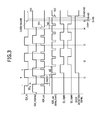
- FIG. 3 is a timing diagram illustrating another example of an operation of the clock detector 100 shown in FIG. 1 .
- the input clock CLK_in may toggle between a high level and a low level to have a cycle time T. If the input clock CLK_in normally toggles, a level of the input clock CLK_in has to regularly and periodically change from a low level to a high level at first, second, third and fourth times “t 1 ”, “t 2 ”, “t 3 ” and “t 4 ”, and a level of the input clock CLK_in has to change from a high level to a low level at a fifth time “t 5 ”.
- a level of the input clock CLK_in normally changes from a low level to a high level at the first, second, third, and fourth points of time “t 1 ”, “t 2 ”, “t 3 ”, and “t 4 ” while the input clock CLK_in abnormally toggles at the fifth time “t 5 ” to cause a clock failure as indicated by a dotted line in FIG. 3 .
- the fifth time “t 5 ” corresponds to a time that a half cycle time T/2 of the input clock CLK_in elapses from the fourth time “t 4 ”.
- the first delay circuit 110 may delay the input clock CLK_in by a first delay time td 1 to generate the delayed clock signal CLK_in(delay).
- the delayed clock signal CLK_in(delay) does not toggle at a time “t 5 +td 1 ” that the first delay time td 1 elapses from the fifth time “t 5 ” either. Accordingly, the delayed clock signal CLK_in(delay) may still maintain a high level even after the fifth time “t 5 ”.
- the first exclusive OR gate 120 may execute an exclusive OR operation on the delayed clock signal CLK_in(delay) and the input clock CLK_in to generate the output signal XOR_out having a plurality of pulses.
- the output signal XOR_out may be generated so that a level of the output signal XOR_out changes from a low level in a high level in synchronization with falling edges and rising edges of the input clock CLK_in and changes from a high level into a low level in synchronization with falling edges and rising edges of the delayed clock signal CLK_in(delay).
- Each of the pulses (having a high level) of the output signal XOR_out may have a width corresponding to the first delay time td 1 .
- the output signal XOR_out of the first exclusive OR gate 120 may maintain a low level without any pulse at the time “t 5 +td 1 ”.
- the second delay circuit 131 may delay the output signal XOR_out by a second delay time td 2 to output the delayed output signal XOR_out.
- the inverter 132 may invert the delayed output signal XOR_out to generate the output signal XOR_out(delay, invert).
- the output signal XOR_out(delay, invert) outputted from the delay/inversion circuit 130 may be a signal that the output signal XOR_out is delayed by the second delay time td 2 and is inverted.
- Each pulse of the output signal XOR_out(delay, invert) outputted from the delay/inversion circuit 130 may have a width corresponding to the first delay time td 1 .
- the second delay time td 2 may be set to be equal to or greater than a half cycle time (T/2) of the input clock CLK_in and to be less than the cycle time (T) of the input clock CLK_in.
- a rising edge i.e., a falling edge or a rising edge of the input clock CLK_in
- a rising edge of one of the pulses of the output signal XOR_out may appear as a falling edge of the output signal XOR_out(delay, invert) through the output terminal of the delay/inversion circuit 130 after the second delay time td 2 which is equal to or greater than a half cycle time (T/2) of the input clock CLK_in and is less than the cycle time (T) of the input clock CLK_in.
- a pulse 302 of the output signal XOR_out(delay, invert) generated from a final pulse 301 of the output signal XOR_out generated before the fifth time “t 5 ” may be located after the fifth time “t 5 ” to overlap with an imaginary pulse 300 of the input clock CLK_in, which is actually absent due to the clock failure.
- the output signal XOR_out(delay, invert) of the delay/inversion circuit 130 may be applied to a clock terminal (i.e., a first clock terminal CK 1 ) of the first flip-flop 140 and a clock terminal (i.e., a second clock terminal CK 2 ) of the second flip-flop 150 . Accordingly, the first and second flip-flops 140 and 150 may operate in synchronization with the output signal XOR_out(delay, invert).
- the first flip-flop 140 may generate the first output signal Q 1 _signal from the input clock CLK_in in synchronization with the output signal XOR_out(delay, invert).
- the first flip-flop 140 may output the first output signal Q 1 _signal having a level of the input clock CLK_in through the first output terminal Q 1 , where the input clock CLK_in is inputted to the first input terminal D 1 of the first flip-flop 140 before a rising edge of the output signal XOR_out(delay, invert). If the pulses of the input clock CLK_in are normally generated, the first output signal Q 1 _signal of the first flip-flop 140 may toggle in synchronization with rising edges of the output signal XOR_out(delay, invert). However, the input clock CLK_in maintains a high level without any pulse from the fifth point of time “t 5 ”.
- the first output signal Q 1 _signal of the first flip-flop 140 may also maintain a high level without toggling at a time “t 4 +td 2 +td 1 ” that a rising edge of the pulse 302 occurs.
- the first output signal Q 1 _signal of the first flip-flop 140 may be inputted to the second input terminal D 2 of the second flip-flop 150 and a first input terminal of the second exclusive OR gate 160 .
- the second flip-flop 150 may generate the second output signal Q 2 _signal from the first output signal Q 1 _signal in synchronization with the output signal XOR_out(delay, invert) through the second output terminal Q 2 , where the second output signal Q 2 _signal may have a level of the first output signal Q 1 _signal inputted to the second input terminal D 2 of the second flip-flop 150 before a rising edge of the output signal XOR_out(delay, invert). If the pulses of the input clock CLK_in are normally generated, the second output signal Q 2 _signal of the second flip-flop 150 may toggle in synchronization with rising edges of the output signal XOR_out(delay, invert).
- the second output signal Q 2 _signal of the second flip-flop 150 may correspond to an inverted first output signal Q 1 _signal of the first flip-flop 140 . Meanwhile, because the first output signal Q 1 _signal of the first flip-flop 140 maintains a high level without toggling from the fifth time “t 5 ”.
- a level of the second output signal Q 2 _signal of the second flip-flop 150 may change from a low level to a high level at the time “t 4 +td 2 +td 1 ” that a rising edge of the pulse 302 occurs.
- the second output signal Q 2 _signal of the second flip-flop 150 may be inputted to a second input terminal of the second exclusive OR gate 160 .
- the second exclusive OR gate 160 may execute an exclusive OR operation on the first output signal Q 1 _signal of the first flip-flop 140 and the second output signal Q 2 _signal of the second flip-flop 150 to generate the clock detection signal. If the first output signal Q 1 _signal of the first flip-flop 140 and the second output signal Q 2 _signal of the second flip-flop 150 have the same level, the second exclusive OR gate 160 may output a low level as the clock detection signal. In contrast, if the first output signal Q 1 _signal of the first flip-flop 140 and the second output signal Q 2 _signal of the second flip-flop 150 have different levels, the second exclusive OR gate 160 may output a high level as the clock detection signal.
- the clock detection signal may maintain a high level from a time that a first rising edge of the output signal XOR_out(delay, invert) occurs.
- the clock detection signal may maintain a high level without toggling during a period in which the pulses of the input clock CLK_in are normally generated.
- both of the first and second output signals Q 1 _signal and Q 2 _signal may have a high level after the fifth time “t 5 ”, particularly, from the time “t 4 +td 2 +td 1 ” that a rising edge of the pulse 302 of the output signal XOR_out(delay, invert) occurs.
- a level of the clock detection signal may change from a high level into a low level at the time “t 4 +td 2 +td 1 ” that a rising edge of the pulse 302 of the output signal XOR_out(delay, invert) occurs. Accordingly, if a level of the clock detection signal changes from a high level to a low level at a certain time, the input clock CLK_in may be regarded as being abnormally generated due to the clock failure from the certain time.
Abstract
A clock detector a first delay circuit delaying an input clock by a first delay time and outputting the delayed input clock as a delayed clock signal, an edge detection circuit receiving the input clock and the delayed clock signal to generate an output signal including pulses which are created in synchronization with edges of the input clock, a delay/inversion circuit delaying the output signal of the edge detection circuit by a second delay time and inverting the delayed output signal to output the inverted signal as an output signal, a first flip-flop receiving the input clock to generate a first output signal, a second flip-flop receiving the first output signal to generate a second output signal, and a clock detection signal generation circuit receiving the first and second output signals to generate a clock detection signal.
Description
The present application claims priority under 35 U.S.C 119(a) to Korean Application No. 10-2016-0104532, filed on Aug. 17, 2016, which is incorporated by reference herein in its entirety.
Various embodiments of the present disclosure relate to clock detectors and, more particularly, to clock detectors including digital logic circuits and methods of detecting clocks.
A system-on-chip (SOC) means an electronic system such as a computer comprised of various electronic circuits which are integrated on a single chip. That is, various functions for processing digital signals, analog signals, composite signals, and/or radio frequency (RF) signals may be realized on a single chip. In such a case, the SOC may require a plurality of clock sources, and the plurality of clock sources may be disposed inside or outside the SOC. While the various kinds of signals are processed in the SOC, it may be necessary to change a current input clock into another input clock. The current input clock may be changed into the other input clock by switching one of the clock sources into another one of the clock sources. In such a case, verifying whether the other input clock is normally generated may be required before switching the clock sources.
Various embodiments are directed to clock detectors and clock detecting methods.
According to an embodiment, a clock detector includes a first delay circuit configured to delay an input clock by a first delay time and configured to output the delayed input clock as a delayed clock signal, an edge detection circuit configured to receive the input clock and the delayed clock signal to generate an output signal including pulses which are created in synchronization with edges of the input clock, a delay/inversion circuit configured to delay the output signal of the edge detection circuit by a second delay time and configured to invert the delayed output signal to output the inverted signal as an output signal, a first flip-flop configured to receive the input clock to generate a first output signal in synchronization with the output signal of the delay/inversion circuit, a second flip-flop configured to receive the first output signal to generate a second output signal in synchronization with the output signal of the delay/inversion circuit, and a clock detection signal generation circuit configured to receive the first output signal and the second output signal to generate a clock detection signal. A level of the clock detection signal changes in a period that a clock failure of the input clock occurs.
According to another embodiment, a clock detecting method includes generating an output signal from an input clock and a delayed clock signal which is delayed from the input clock by a first delay time. The output signal is generated in synchronization with rising edges and falling edges of the input clock. The output signal is delayed by a second delay time to generate a delayed output signal, and the delayed pulse signal is inverted to generate a delayed/inverted clock signal. A first output signal is generated from the input clock in synchronization with the delayed/inverted clock signal. A second output signal is generated from the first output signal in synchronization with the delayed/inverted clock signal. A logical operation of the first output signal and the second output signal is executed to generate a clock detection signal. A level of the clock detection signal changes in a period that a clock failure of the input clock occurs.
Various embodiments of the present disclosure will become more apparent in view of the attached drawings and accompanying detailed description, in which:
In the following description of the embodiments, it will be understood that the terms “first” and “second” are intended to identify an element, but not used to define only the element itself or to mean a particular sequence. In addition, when an element is referred to as being located “on”, “over”, “above”, “under” or “beneath” another element, it is intended to mean relative position relationship, but not used to limit certain cases that the element directly contacts the other element, or at least one intervening element is present therebetween. Accordingly, the terms such as “on”, “over”, “above”, “under”, “beneath”, “below” and the like that are used herein are for the purpose of describing particular embodiments only and are not intended to limit the scope of the present disclosure. Further, when an element is referred to as being “connected” or “coupled” to another element, the element may be electrically or mechanically connected or coupled to the other element directly, or may form a connection relationship or coupling relationship by replacing the other element therebetween.
The first delay circuit 110 receiving the input clock CLK_in may delay the input clock CLK_in by a certain delay time to output the delayed input clock as a delayed clock signal CLK_in(delay). The input clock CLK_in may be inputted to a first input terminal of the first exclusive OR gate 120, and the delayed clock signal CLK_in(delay) outputted from the first delay circuit 110 may be inputted to a second input terminal of the first exclusive OR gate 120. The first exclusive OR gate 120 may output an output signal XOR_out including pulses which are generated in synchronization with rising edges and falling edges of the input clock CLK_in. An output terminal of the first exclusive OR gate 120 may be coupled to an input terminal of the delay/inversion circuit 130. The delay/inversion circuit 130 may be configured to include a second delay circuit 131 and an inverter 132 which are coupled in series. An input terminal of the second delay circuit 131 may be coupled to the output terminal of the first exclusive OR gate 120. The second delay circuit 131 may delay the output signal XOR_out of the first exclusive OR gate 120 by a certain delay time to output a delayed output signal. The second delay circuit 131 may be designed so that a delay time of the second delay circuit 131 is equal to or greater than a half cycle time (T/2) of the input clock CLK_in and is less than the cycle time (T) of the input clock CLK_in. An output terminal of the second delay circuit 131 may be coupled to an input terminal of the inverter 132. The inverter 132 may invert a delayed output signal of the second delay circuit 131 and may output an inverted output signal as an output signal XOR_out(delay, invert) of the delay/inversion circuit 130.
The output signal XOR_out(delay, invert) of the delay/inversion circuit 130 may be used as the clock signal of the first and second flip- flops 140 and 150. The output signal XOR_out(delay, invert) of the delay/inversion circuit 130 may be generated from the input clock CLK_in through the first delay circuit 110, the first exclusive OR gate 120, and the delay/inversion circuit 130. Thus, the first and second flip- flops 140 and 150 may be triggered by the output signal XOR_out(delay, invert) even without any external clock signal. Each of the first and second flip- flops 140 and 150 may be a D flip-flop which is triggered at rising edges of the output signal XOR_out(delay, invert) of the delay/inversion circuit 130. The input clock CLK_in may be directly inputted to an input terminal (i.e., a first input terminal D1) of the first flip-flop 140 to generate an output signal Q1_signal in synchronization with the output signal XOR_out(delay, invert) of the delay/inversion circuit 130. The output signal Q1_signal outputted from an output terminal Q1 of the first flip-flop 140 may be inputted to an input terminal (i.e., a second input terminal D2) of the second flip-flop 150 to generate an output signal Q2_signal in synchronization with the output signal XOR_out(delay, invert) of the delay/inversion circuit 130. The second input terminal D2 may be coupled to the output terminal Q1. The output signal Q1_signal of the first flip-flop 140 may also be inputted to a first input terminal of the second exclusive OR gate 160 and the output signal Q2_signal of the second flip-flop 150 may be inputted to a second input terminal of the second exclusive OR gate 160 to generate the clock detection signal. The second flip-flop 150 may output the output signal Q2_signal through an output terminal Q2. The second exclusive OR gate 160 may generate the clock detection signal, which changes from a high level to a low level, if the input clock CLK_in is abnormally generated. In other words, the second exclusive OR gate 160 may generate the clock detection signal which changes from a high level to a low level in the period that the clock failure of the input clock CLK_in occurs.
The first exclusive OR gate 120 may execute an exclusive OR operation on the delayed clock signal CLK_in(delay) and the input clock CLK_in to generate the output signal XOR_out having a plurality of pulses. The output signal XOR_out may be generated so that a level of the output signal XOR_out changes from a low level to a high level in synchronization with falling edges and rising edges of the input clock CLK_in and changes from a high level to a low level in synchronization with falling edges and rising edges of the delayed clock signal CLK_in(delay). Each of the pulses of the output signal XOR_out may have a width corresponding to the first delay time td1. Because the delayed clock signal CLK_in(delay) does not toggle at a time that the first delay time td1 elapses from the fourth time “t4”, the output signal XOR_out of the first exclusive OR gate 120 may maintain a low level without any pulse at a time “t4+td1”.
The second delay circuit 131 may delay the output signal XOR_out by a second delay time td2 to output the delayed output signal XOR_out. The inverter 132 may invert the delayed output signal XOR_out to generate the output signal XOR_out(delay, invert). Thus, the output signal XOR_out(delay, invert) outputted from the delay/inversion circuit 130 may be a signal in which the output signal XOR_out is delayed by the second delay time td2 and is inverted. Each pulse of the output signal XOR_out(delay, invert) outputted from the delay/inversion circuit 130 may have a width corresponding to the first delay time td1. The second delay time td2 may be set to be equal to or greater than a half cycle time (T/2) of the input clock CLK_in and to be less than the cycle time (T) of the input clock CLK_in. Thus, a rising edge (i.e., a falling edge or a rising edge of the input clock CLK_in) of one of the pulses of the output signal XOR_out may appear as a falling edge of the output signal XOR_out(delay, invert) through the output terminal of the delay/inversion circuit 130 after the second delay time td2 which is equal to or greater than a half cycle time (T/2) of the input clock CLK_in and is less than the cycle time (T) of the input clock CLK_in. Accordingly, a pulse 202 of the output signal XOR_out(delay, invert) generated from a final pulse 201 of the output signal XOR_out generated before the fourth time “t4” may be located after the fourth time “t4” to overlap with an imaginary pulse 200 of the input clock CLK_in, which is actually absent due to the clock failure.
The output signal XOR_out(delay, invert) of the delay/inversion circuit 130 may be applied to a clock terminal (i.e., a first clock terminal CK1) of the first flip-flop 140 and a clock terminal (i.e., a second clock terminal CK2) of the second flip-flop 150. Accordingly, the first and second flip- flops 140 and 150 may operate in synchronization with the output signal XOR_out(delay, invert). The first flip-flop 140 may generate the first output signal Q1_signal from the input clock CLK_in in synchronization with the output signal XOR_out(delay, invert). Specifically, the first flip-flop 140 may output the first output signal Q1_signal having a level of the input clock CLK_in through the first output terminal Q1, where the input clock CLK_in is inputted to the first input terminal D1 of the first flip-flop 140 before a rising edge of the output signal XOR_out(delay, invert). If the pulses of the input clock CLK_in are normally generated, the first output signal Q1_signal of the first flip-flop 140 may toggle in synchronization with rising edges of the output signal XOR_out(delay, invert). However, because the input clock CLK_in maintains a low level without any pulse from the fourth time “t4”, the first output signal Q1_signal of the first flip-flop 140 may maintain a low level without toggling even though the pulse 202 of the output signal XOR_out(delay, invert) is inputted to the first flip-flop 140 after the fourth time “t4”. The first output signal Q1_signal of the first flip-flop 140 may be inputted to the second input terminal D2 of the second flip-flop 150 and a first input terminal of the second exclusive OR gate 160.
The second flip-flop 150 may generate the second output signal Q2_signal from the first output signal Q1_signal in synchronization with the output signal XOR_out(delay, invert) through the second output terminal Q2, where the second output signal Q2_signal may have a level of the first output signal Q1_signal inputted to the second input terminal D2 of the second flip-flop 150 before a rising edge of the output signal XOR_out(delay, invert). If the pulses of the input clock CLK_in are normally generated, the second output signal Q2_signal of the second flip-flop 150 may toggle in synchronization with rising edges of the output signal XOR_out(delay, invert). Because the first output signal Q1_signal of the first flip-flop 140 is inputted to the second input terminal D2 of the second flip-flop 150, the second output signal Q2_signal of the second flip-flop 150 may correspond to an inverted first output signal Q1_signal of the first flip-flop 140. Meanwhile, because the first output signal Q1_signal of the first flip-flop 140 maintains a low level without toggling from the fourth time “t4”, a level of the second output signal Q2_signal of the second flip-flop 150 may change from a high level to a low level in synchronization with a rising edge of the pulse 202 of the output signal XOR_out(delay, invert) if the pulse 202 is inputted to the second flip-flop 150 after the fourth time “t4”. The second output signal Q2_signal of the second flip-flop 150 may be inputted to a second input terminal of the second exclusive OR gate 160.
The second exclusive OR gate 160 may execute an exclusive OR operation on the first output signal Q1_signal of the first flip-flop 140 and the second output signal Q2_signal of the second flip-flop 150 to generate the clock detection signal. If the first output signal Q1_signal of the first flip-flop 140 and the second output signal Q2_signal of the second flip-flop 150 have the same level, the second exclusive OR gate 160 may output a low level as the clock detection signal. In contrast, if the first output signal Q1_signal of the first flip-flop 140 and the second output signal Q2_signal of the second flip-flop 150 have different levels, the second exclusive OR gate 160 may output a high level as the clock detection signal. Thus, the clock detection signal may maintain a high level from a time that a first rising edge of the output signal XOR_out(delay, invert) occurs. The clock detection signal may maintain a high level without toggling during a period in which the pulses of the input clock CLK_in are normally generated. However, both of the first and second output signals Q1_signal and Q2_signal may have a low level after the fourth time “t4”, particularly, from a time that a rising edge of the pulse 202 of the output signal XOR_out(delay, invert) occurs. Thus, a level of the clock detection signal may change from a high level into a low level at the time that a rising edge of the pulse 202 of the output signal XOR_out(delay, invert) occurs. Accordingly, if a level of the clock detection signal changes from a high level to a low level at a certain time, the input clock CLK_in may be regarded as being abnormally generated due to the clock failure from the certain time.
The first exclusive OR gate 120 may execute an exclusive OR operation on the delayed clock signal CLK_in(delay) and the input clock CLK_in to generate the output signal XOR_out having a plurality of pulses. The output signal XOR_out may be generated so that a level of the output signal XOR_out changes from a low level in a high level in synchronization with falling edges and rising edges of the input clock CLK_in and changes from a high level into a low level in synchronization with falling edges and rising edges of the delayed clock signal CLK_in(delay). Each of the pulses (having a high level) of the output signal XOR_out may have a width corresponding to the first delay time td1. Because the delayed clock signal CLK_in(delay) does not toggle at the time “t5+td1” that the first delay time td1 elapses from the fifth time “t5”, the output signal XOR_out of the first exclusive OR gate 120 may maintain a low level without any pulse at the time “t5+td1”.
The second delay circuit 131 may delay the output signal XOR_out by a second delay time td2 to output the delayed output signal XOR_out. The inverter 132 may invert the delayed output signal XOR_out to generate the output signal XOR_out(delay, invert). Thus, the output signal XOR_out(delay, invert) outputted from the delay/inversion circuit 130 may be a signal that the output signal XOR_out is delayed by the second delay time td2 and is inverted. Each pulse of the output signal XOR_out(delay, invert) outputted from the delay/inversion circuit 130 may have a width corresponding to the first delay time td1. The second delay time td2 may be set to be equal to or greater than a half cycle time (T/2) of the input clock CLK_in and to be less than the cycle time (T) of the input clock CLK_in. Thus, a rising edge (i.e., a falling edge or a rising edge of the input clock CLK_in) of one of the pulses of the output signal XOR_out may appear as a falling edge of the output signal XOR_out(delay, invert) through the output terminal of the delay/inversion circuit 130 after the second delay time td2 which is equal to or greater than a half cycle time (T/2) of the input clock CLK_in and is less than the cycle time (T) of the input clock CLK_in. Accordingly, a pulse 302 of the output signal XOR_out(delay, invert) generated from a final pulse 301 of the output signal XOR_out generated before the fifth time “t5” may be located after the fifth time “t5” to overlap with an imaginary pulse 300 of the input clock CLK_in, which is actually absent due to the clock failure.
The output signal XOR_out(delay, invert) of the delay/inversion circuit 130 may be applied to a clock terminal (i.e., a first clock terminal CK1) of the first flip-flop 140 and a clock terminal (i.e., a second clock terminal CK2) of the second flip-flop 150. Accordingly, the first and second flip- flops 140 and 150 may operate in synchronization with the output signal XOR_out(delay, invert). The first flip-flop 140 may generate the first output signal Q1_signal from the input clock CLK_in in synchronization with the output signal XOR_out(delay, invert). Specifically, the first flip-flop 140 may output the first output signal Q1_signal having a level of the input clock CLK_in through the first output terminal Q1, where the input clock CLK_in is inputted to the first input terminal D1 of the first flip-flop 140 before a rising edge of the output signal XOR_out(delay, invert). If the pulses of the input clock CLK_in are normally generated, the first output signal Q1_signal of the first flip-flop 140 may toggle in synchronization with rising edges of the output signal XOR_out(delay, invert). However, the input clock CLK_in maintains a high level without any pulse from the fifth point of time “t5”. Thus, even though the pulse 302 of the output signal XOR_out(delay, invert) is inputted to the first flip-flop 140 after the fifth point of time “t5”, the first output signal Q1_signal of the first flip-flop 140 may also maintain a high level without toggling at a time “t4+td2+td1” that a rising edge of the pulse 302 occurs. The first output signal Q1_signal of the first flip-flop 140 may be inputted to the second input terminal D2 of the second flip-flop 150 and a first input terminal of the second exclusive OR gate 160.
The second flip-flop 150 may generate the second output signal Q2_signal from the first output signal Q1_signal in synchronization with the output signal XOR_out(delay, invert) through the second output terminal Q2, where the second output signal Q2_signal may have a level of the first output signal Q1_signal inputted to the second input terminal D2 of the second flip-flop 150 before a rising edge of the output signal XOR_out(delay, invert). If the pulses of the input clock CLK_in are normally generated, the second output signal Q2_signal of the second flip-flop 150 may toggle in synchronization with rising edges of the output signal XOR_out(delay, invert). Because the first output signal Q1_signal of the first flip-flop 140 is inputted to the second input terminal D2 of the second flip-flop 150, the second output signal Q2_signal of the second flip-flop 150 may correspond to an inverted first output signal Q1_signal of the first flip-flop 140. Meanwhile, because the first output signal Q1_signal of the first flip-flop 140 maintains a high level without toggling from the fifth time “t5”. Thus, if the pulse 302 of the output signal XOR_out(delay, invert) is inputted to the second flip-flop 150 after the fifth time “t5”, a level of the second output signal Q2_signal of the second flip-flop 150 may change from a low level to a high level at the time “t4+td2+td1” that a rising edge of the pulse 302 occurs. The second output signal Q2_signal of the second flip-flop 150 may be inputted to a second input terminal of the second exclusive OR gate 160.
The second exclusive OR gate 160 may execute an exclusive OR operation on the first output signal Q1_signal of the first flip-flop 140 and the second output signal Q2_signal of the second flip-flop 150 to generate the clock detection signal. If the first output signal Q1_signal of the first flip-flop 140 and the second output signal Q2_signal of the second flip-flop 150 have the same level, the second exclusive OR gate 160 may output a low level as the clock detection signal. In contrast, if the first output signal Q1_signal of the first flip-flop 140 and the second output signal Q2_signal of the second flip-flop 150 have different levels, the second exclusive OR gate 160 may output a high level as the clock detection signal. Thus, the clock detection signal may maintain a high level from a time that a first rising edge of the output signal XOR_out(delay, invert) occurs. The clock detection signal may maintain a high level without toggling during a period in which the pulses of the input clock CLK_in are normally generated. However, both of the first and second output signals Q1_signal and Q2_signal may have a high level after the fifth time “t5”, particularly, from the time “t4+td2+td1” that a rising edge of the pulse 302 of the output signal XOR_out(delay, invert) occurs. Thus, a level of the clock detection signal may change from a high level into a low level at the time “t4+td2+td1” that a rising edge of the pulse 302 of the output signal XOR_out(delay, invert) occurs. Accordingly, if a level of the clock detection signal changes from a high level to a low level at a certain time, the input clock CLK_in may be regarded as being abnormally generated due to the clock failure from the certain time.
The embodiments of the present disclosure have been disclosed above for illustrative purposes. Those of ordinary skill in the art will appreciate that various modifications, additions, and substitutions are possible, without departing from the scope and spirit of the present disclosure as disclosed in the accompanying claims.
Claims (20)
1. A clock detector comprising;
a first delay circuit configured to delay an input clock by a first delay time and configured to output the delayed input clock as a delayed clock signal;
an edge detection circuit configured to receive the input clock and the delayed clock signal to generate an output signal including pulses which are created in synchronization with edges of the input clock;
a delay/inversion circuit configured to delay the output signal of the edge detection circuit by a second delay time and configured to invert the delayed output signal to output the inverted signal as an output signal;
a first flip-flop configured to receive the input clock to generate a first output signal in synchronization with the output signal of the delay/inversion circuit;
a second flip-flop configured to receive the first output signal to generate a second output signal in synchronization with the output signal of the delay/inversion circuit; and
a clock detection signal generation circuit configured to receive the first output signal and the second output signal to generate a clock detection signal, a level of which changes in a period that a clock failure of the input clock occurs.
2. The clock detector of claim 1 , wherein the edge detection circuit comprises a first exclusive OR gate.
3. The clock detector of claim 1 , wherein the delay/inversion circuit includes:
a second delay circuit configured to delay the output signal of the edge detection circuit by the second delay time to output the delayed signal; and
an inverter configured to invert the output signal of the second delay circuit to output the inverted signal as an output signal.
4. The clock detector of claim 3 , wherein the second delay time is equal to or greater than a half cycle time of the input clock and is less than a cycle time of the input clock.
5. The clock detector of claim 1 , wherein each of the first and second flip-flops comprises a D flip-flop.
6. The clock detector of claim 5 , wherein the D flip-flop is triggered at rising edges of the output signal of the delay/inversion circuit.
7. The clock detector of claim 6 , wherein the first flip-flop includes a first clock terminal to which the output signal of the delay/inversion circuit is applied, a first input terminal to which the input clock is applied, and a first output terminal through which the first output signal is outputted.
8. The clock detector of claim 7 , wherein the second flip-flop includes a second clock terminal to which the output signal of the delay/inversion circuit is applied, a second input terminal coupled to the first output terminal, and a second output terminal through which the second output signal is outputted.
9. The clock detector of claim 8 , wherein the clock detection signal generation circuit comprises a second exclusive OR gate.
10. The clock detector of claim 9 , wherein the second exclusive OR gate generates the clock detection signal, a level of which changes in a period that a clock failure of the input clock occurs.
11. The clock detector of claim 10 , wherein a level of the clock detection signal changes from a high level to a low level in the period that the clock failure of the input clock occurs.
12. A clock detection method comprising:
generating an output signal from an input clock and a delayed clock signal delayed from the input clock by a first delay time, wherein the output signal is generated in synchronization with rising edges and falling edges of the input clock;
delaying the output signal by a second delay time and inverting the delayed output signal to generate a delayed/inverted clock signal;
generating a first output signal from the input clock in synchronization with the delayed/inverted clock signal;
generating a second output signal from the first output signal in synchronization with the delayed/inverted clock signal; and
executing a logical operation of the first output signal and the second output signal to generate a clock detection signal, a level of which changes in a period that a clock failure of the input clock occurs.
13. The clock detection method of claim 12 , wherein generating the output signal includes executing an exclusive OR operation on the input clock and the delayed clock signal.
14. The clock detection method of claim 12 , wherein the second delay time is set to be equal to or greater than a half cycle time of the input clock and to be less than a cycle time of the input clock.
15. The clock detection method of claim 12 , wherein the first output signal is generated by a first D flip-flop having a first clock terminal to which the delayed/inverted clock signal is applied, a first input terminal to which the input clock is applied, and a first output terminal through which the first output signal is outputted.
16. The clock detection method of claim 15 , wherein the first D flip-flop is triggered at rising edges of the output signal of a delay/inversion circuit.
17. The clock detection method of claim 12 , wherein the second output signal is generated by a second D flip-flop having a second clock terminal to which the delayed/inverted clock signal is applied, a second input terminal to which the first output signal is applied, and a second output terminal through which the second output signal is outputted.
18. The clock detection method of claim 17 , wherein the second D flip-flop is triggered at rising edges of the output signal of the delayed/inverted clock signal.
19. The clock detection method of claim 12 , wherein the clock detection signal is generated by executing an exclusive OR operation of the first output signal and the second output signal.
20. The clock detection method of claim 12 , wherein a level of the clock detection signal changes from a high level in a low level in a period that a clock failure of the input clock occurs.
Applications Claiming Priority (3)
| Application Number | Priority Date | Filing Date | Title |
|---|---|---|---|
| KR1020160104532A KR102491690B1 (en) | 2016-08-17 | 2016-08-17 | Clock detector and clock detecting method |
| KR10-2016-0104532 | 2016-08-17 | ||
| KR1020160104532 | 2016-08-17 |
Publications (2)
| Publication Number | Publication Date |
|---|---|
| US20180054193A1 US20180054193A1 (en) | 2018-02-22 |
| US10014849B2 true US10014849B2 (en) | 2018-07-03 |
Family
ID=61192272
Family Applications (1)
| Application Number | Title | Priority Date | Filing Date |
|---|---|---|---|
| US15/440,339 Active US10014849B2 (en) | 2016-08-17 | 2017-02-23 | Clock detectors and methods of detecting clocks |
Country Status (2)
| Country | Link |
|---|---|
| US (1) | US10014849B2 (en) |
| KR (1) | KR102491690B1 (en) |
Cited By (2)
| Publication number | Priority date | Publication date | Assignee | Title |
|---|---|---|---|---|
| US10848140B1 (en) | 2020-07-20 | 2020-11-24 | Nxp Usa, Inc. | Method and system for detecting clock failure |
| US11736099B1 (en) * | 2022-08-14 | 2023-08-22 | Nanya Technology Corporation | Clock detecting circuit |
Citations (13)
| Publication number | Priority date | Publication date | Assignee | Title |
|---|---|---|---|---|
| US5164966A (en) * | 1991-03-07 | 1992-11-17 | The Grass Valley Group, Inc. | Nrz clock and data recovery system employing phase lock loop |
| US5619171A (en) * | 1994-09-28 | 1997-04-08 | U.S. Philips Corporation | Phase-locked loop, phase comparator for use in the phase-locked loop, and reproducing device including the phase-locked loop |
| US6064236A (en) * | 1997-10-17 | 2000-05-16 | Fujtisu Limited | Phase detector and timing extracting circuit using phase detector |
| KR100278269B1 (en) | 1997-12-30 | 2001-01-15 | 김영환 | A circuit for detecting reset signal using clock signal |
| US6583653B1 (en) * | 2000-03-31 | 2003-06-24 | Intel Corporation | Method and apparatus for generating a clock signal |
| US20040114702A1 (en) | 2002-12-12 | 2004-06-17 | International Business Machines Corporation | Bang-bang phase detector for full-rate and half-rate schemes clock and data recovery and method therefor |
| US20050008112A1 (en) * | 2001-12-27 | 2005-01-13 | Yasuhito Takeo | Phase synchronization circuit |
| US20050068060A1 (en) * | 2003-08-07 | 2005-03-31 | Takeshi Ooshita | Transmission signal correction circuit |
| US20100073058A1 (en) * | 2007-03-12 | 2010-03-25 | Yusuke Ohtomo | Clock/data recovery circuit |
| US20100301950A1 (en) * | 2009-06-02 | 2010-12-02 | Sony Corporation | Clock regeneration apparatus and electric equipment |
| US8350596B1 (en) * | 2010-03-26 | 2013-01-08 | Altera Corporation | Clock loss detection circuit for PLL clock switchover |
| US20130076426A1 (en) * | 2011-09-28 | 2013-03-28 | Altek Corporation | Apparatus for supplying clock and method thereof |
| US20140266369A1 (en) * | 2013-03-15 | 2014-09-18 | Qualcomm Incorporated | Low power architectures |
Family Cites Families (2)
| Publication number | Priority date | Publication date | Assignee | Title |
|---|---|---|---|---|
| KR100498229B1 (en) * | 2002-10-17 | 2005-07-01 | 광주과학기술원 | Apparatus for burst-mode clock and data recovery employing jitter reduction method |
| TWI300293B (en) | 2005-10-07 | 2008-08-21 | Ind Tech Res Inst | Clock generator and data recovery circuit utilizing the same |
-
2016
- 2016-08-17 KR KR1020160104532A patent/KR102491690B1/en active IP Right Grant
-
2017
- 2017-02-23 US US15/440,339 patent/US10014849B2/en active Active
Patent Citations (14)
| Publication number | Priority date | Publication date | Assignee | Title |
|---|---|---|---|---|
| US5164966A (en) * | 1991-03-07 | 1992-11-17 | The Grass Valley Group, Inc. | Nrz clock and data recovery system employing phase lock loop |
| US5619171A (en) * | 1994-09-28 | 1997-04-08 | U.S. Philips Corporation | Phase-locked loop, phase comparator for use in the phase-locked loop, and reproducing device including the phase-locked loop |
| US6064236A (en) * | 1997-10-17 | 2000-05-16 | Fujtisu Limited | Phase detector and timing extracting circuit using phase detector |
| KR100278269B1 (en) | 1997-12-30 | 2001-01-15 | 김영환 | A circuit for detecting reset signal using clock signal |
| US6583653B1 (en) * | 2000-03-31 | 2003-06-24 | Intel Corporation | Method and apparatus for generating a clock signal |
| US20050008112A1 (en) * | 2001-12-27 | 2005-01-13 | Yasuhito Takeo | Phase synchronization circuit |
| US20040114702A1 (en) | 2002-12-12 | 2004-06-17 | International Business Machines Corporation | Bang-bang phase detector for full-rate and half-rate schemes clock and data recovery and method therefor |
| US20050068060A1 (en) * | 2003-08-07 | 2005-03-31 | Takeshi Ooshita | Transmission signal correction circuit |
| US20100073058A1 (en) * | 2007-03-12 | 2010-03-25 | Yusuke Ohtomo | Clock/data recovery circuit |
| US20100301950A1 (en) * | 2009-06-02 | 2010-12-02 | Sony Corporation | Clock regeneration apparatus and electric equipment |
| US8125278B2 (en) * | 2009-06-02 | 2012-02-28 | Sony Corporation | Clock regeneration apparatus and electric equipment |
| US8350596B1 (en) * | 2010-03-26 | 2013-01-08 | Altera Corporation | Clock loss detection circuit for PLL clock switchover |
| US20130076426A1 (en) * | 2011-09-28 | 2013-03-28 | Altek Corporation | Apparatus for supplying clock and method thereof |
| US20140266369A1 (en) * | 2013-03-15 | 2014-09-18 | Qualcomm Incorporated | Low power architectures |
Cited By (2)
| Publication number | Priority date | Publication date | Assignee | Title |
|---|---|---|---|---|
| US10848140B1 (en) | 2020-07-20 | 2020-11-24 | Nxp Usa, Inc. | Method and system for detecting clock failure |
| US11736099B1 (en) * | 2022-08-14 | 2023-08-22 | Nanya Technology Corporation | Clock detecting circuit |
Also Published As
| Publication number | Publication date |
|---|---|
| KR20180020048A (en) | 2018-02-27 |
| KR102491690B1 (en) | 2023-01-26 |
| US20180054193A1 (en) | 2018-02-22 |
Similar Documents
| Publication | Publication Date | Title |
|---|---|---|
| US9092013B2 (en) | Time-to-digital converter | |
| US9685953B1 (en) | Low latency asynchronous interface circuits | |
| CN110311659B (en) | Trigger and integrated circuit | |
| US10014849B2 (en) | Clock detectors and methods of detecting clocks | |
| CN107046416B (en) | Duty ratio correction circuit | |
| US10256823B2 (en) | Clock generation circuit | |
| JP2007157147A (en) | Circuit and method for time-stamping event for fraction of clock cycle | |
| US8975921B1 (en) | Synchronous clock multiplexer | |
| US6873183B1 (en) | Method and circuit for glitchless clock control | |
| US10848140B1 (en) | Method and system for detecting clock failure | |
| US9991876B2 (en) | Master-slave flip-flop | |
| US10243545B2 (en) | Shift register utilizing latches controlled by dual non-overlapping clocks | |
| US11073862B2 (en) | Synchronization circuit and cascaded synchronization circuit for converting asynchronous signal into synchronous signal | |
| US7042267B1 (en) | Gated clock circuit with a substantially increased control signal delay | |
| US10256800B1 (en) | Delay-locked loop circuit and selection method of unit coarse delay thereof | |
| US20150171832A1 (en) | Clock regenerator | |
| US8258838B2 (en) | Delay locked loop for expanding a delay range | |
| US8890594B1 (en) | System for functional reset across multiple clock domains | |
| CN111262562B (en) | Metastable state detection circuit | |
| US7400178B2 (en) | Data output clock selection circuit for quad-data rate interface | |
| US8773180B2 (en) | Device for generating reset signal having sufficient pulse width | |
| KR102002466B1 (en) | Digital counter | |
| US10454457B1 (en) | Self-gating flip-flop | |
| US10157087B1 (en) | Robust boot block design and architecture | |
| US10110228B2 (en) | Semiconductor device |
Legal Events
| Date | Code | Title | Description |
|---|---|---|---|
| AS | Assignment |
Owner name: SK HYNIX INC., KOREA, REPUBLIC OF Free format text: ASSIGNMENT OF ASSIGNORS INTEREST;ASSIGNOR:NOH, HYUNJIN;REEL/FRAME:041357/0565 Effective date: 20170214 |
|
| STCF | Information on status: patent grant |
Free format text: PATENTED CASE |
|
| MAFP | Maintenance fee payment |
Free format text: PAYMENT OF MAINTENANCE FEE, 4TH YEAR, LARGE ENTITY (ORIGINAL EVENT CODE: M1551); ENTITY STATUS OF PATENT OWNER: LARGE ENTITY Year of fee payment: 4 |