KR20230017312A - Metal strip surface inspection device, surface inspection method, and manufacturing method - Google Patents
Metal strip surface inspection device, surface inspection method, and manufacturing method Download PDFInfo
- Publication number
- KR20230017312A KR20230017312A KR1020227046286A KR20227046286A KR20230017312A KR 20230017312 A KR20230017312 A KR 20230017312A KR 1020227046286 A KR1020227046286 A KR 1020227046286A KR 20227046286 A KR20227046286 A KR 20227046286A KR 20230017312 A KR20230017312 A KR 20230017312A
- Authority
- KR
- South Korea
- Prior art keywords
- light
- metal strip
- light source
- source unit
- unit
- Prior art date
Links
- 239000002184 metal Substances 0.000 title claims abstract description 216
- 229910052751 metal Inorganic materials 0.000 title claims abstract description 216
- 238000007689 inspection Methods 0.000 title claims abstract description 45
- 238000000034 method Methods 0.000 title claims description 47
- 238000004519 manufacturing process Methods 0.000 title claims description 37
- 230000007547 defect Effects 0.000 claims abstract description 287
- 238000003384 imaging method Methods 0.000 claims abstract description 144
- 230000003287 optical effect Effects 0.000 claims description 100
- 230000001678 irradiating effect Effects 0.000 claims description 7
- 238000001514 detection method Methods 0.000 description 31
- 238000012545 processing Methods 0.000 description 22
- 238000009826 distribution Methods 0.000 description 21
- 230000000875 corresponding effect Effects 0.000 description 15
- 230000035945 sensitivity Effects 0.000 description 13
- 238000005096 rolling process Methods 0.000 description 12
- 238000001228 spectrum Methods 0.000 description 12
- 229910000831 Steel Inorganic materials 0.000 description 11
- 239000010959 steel Substances 0.000 description 11
- 238000010586 diagram Methods 0.000 description 9
- 239000000047 product Substances 0.000 description 9
- 230000003595 spectral effect Effects 0.000 description 9
- 238000003860 storage Methods 0.000 description 8
- 230000000052 comparative effect Effects 0.000 description 7
- 238000007747 plating Methods 0.000 description 7
- 238000000137 annealing Methods 0.000 description 6
- 238000005097 cold rolling Methods 0.000 description 6
- 239000003086 colorant Substances 0.000 description 6
- 239000010408 film Substances 0.000 description 5
- 230000010365 information processing Effects 0.000 description 5
- 230000006870 function Effects 0.000 description 4
- 238000005098 hot rolling Methods 0.000 description 4
- 238000000926 separation method Methods 0.000 description 4
- 230000005540 biological transmission Effects 0.000 description 3
- 238000011109 contamination Methods 0.000 description 3
- 238000011143 downstream manufacturing Methods 0.000 description 3
- 230000000694 effects Effects 0.000 description 3
- JEIPFZHSYJVQDO-UHFFFAOYSA-N iron(III) oxide Inorganic materials O=[Fe]O[Fe]=O JEIPFZHSYJVQDO-UHFFFAOYSA-N 0.000 description 3
- 238000005554 pickling Methods 0.000 description 3
- 238000000275 quality assurance Methods 0.000 description 3
- 239000000126 substance Substances 0.000 description 3
- 238000004364 calculation method Methods 0.000 description 2
- 239000011248 coating agent Substances 0.000 description 2
- 238000000576 coating method Methods 0.000 description 2
- 230000006835 compression Effects 0.000 description 2
- 238000007906 compression Methods 0.000 description 2
- 239000012467 final product Substances 0.000 description 2
- 230000001788 irregular Effects 0.000 description 2
- 239000000463 material Substances 0.000 description 2
- 238000005259 measurement Methods 0.000 description 2
- 238000000465 moulding Methods 0.000 description 2
- 208000032544 Cicatrix Diseases 0.000 description 1
- RYGMFSIKBFXOCR-UHFFFAOYSA-N Copper Chemical compound [Cu] RYGMFSIKBFXOCR-UHFFFAOYSA-N 0.000 description 1
- 229910001335 Galvanized steel Inorganic materials 0.000 description 1
- 235000000177 Indigofera tinctoria Nutrition 0.000 description 1
- 230000002159 abnormal effect Effects 0.000 description 1
- 238000005299 abrasion Methods 0.000 description 1
- 238000010521 absorption reaction Methods 0.000 description 1
- 229910052782 aluminium Inorganic materials 0.000 description 1
- XAGFODPZIPBFFR-UHFFFAOYSA-N aluminium Chemical compound [Al] XAGFODPZIPBFFR-UHFFFAOYSA-N 0.000 description 1
- 238000004458 analytical method Methods 0.000 description 1
- 238000003705 background correction Methods 0.000 description 1
- 230000015572 biosynthetic process Effects 0.000 description 1
- 238000004140 cleaning Methods 0.000 description 1
- 238000004590 computer program Methods 0.000 description 1
- 238000013527 convolutional neural network Methods 0.000 description 1
- 229910052802 copper Inorganic materials 0.000 description 1
- 239000010949 copper Substances 0.000 description 1
- 230000002596 correlated effect Effects 0.000 description 1
- 238000013135 deep learning Methods 0.000 description 1
- 230000002950 deficient Effects 0.000 description 1
- 230000008021 deposition Effects 0.000 description 1
- 230000000994 depressogenic effect Effects 0.000 description 1
- 230000006866 deterioration Effects 0.000 description 1
- 238000010790 dilution Methods 0.000 description 1
- 239000012895 dilution Substances 0.000 description 1
- 238000009713 electroplating Methods 0.000 description 1
- 238000005516 engineering process Methods 0.000 description 1
- 230000001747 exhibiting effect Effects 0.000 description 1
- 230000004438 eyesight Effects 0.000 description 1
- 239000008397 galvanized steel Substances 0.000 description 1
- 238000005246 galvanizing Methods 0.000 description 1
- 229940097275 indigo Drugs 0.000 description 1
- COHYTHOBJLSHDF-UHFFFAOYSA-N indigo powder Natural products N1C2=CC=CC=C2C(=O)C1=C1C(=O)C2=CC=CC=C2N1 COHYTHOBJLSHDF-UHFFFAOYSA-N 0.000 description 1
- 238000009434 installation Methods 0.000 description 1
- 239000011229 interlayer Substances 0.000 description 1
- 238000011835 investigation Methods 0.000 description 1
- 238000010801 machine learning Methods 0.000 description 1
- 239000002923 metal particle Substances 0.000 description 1
- 239000002245 particle Substances 0.000 description 1
- 239000011295 pitch Substances 0.000 description 1
- 238000007781 pre-processing Methods 0.000 description 1
- 230000004800 psychological effect Effects 0.000 description 1
- 231100000241 scar Toxicity 0.000 description 1
- 230000037387 scars Effects 0.000 description 1
- 239000004065 semiconductor Substances 0.000 description 1
- 238000004611 spectroscopical analysis Methods 0.000 description 1
- 238000009628 steelmaking Methods 0.000 description 1
- 230000002194 synthesizing effect Effects 0.000 description 1
- 239000010409 thin film Substances 0.000 description 1
- 238000012546 transfer Methods 0.000 description 1
- 238000011179 visual inspection Methods 0.000 description 1
- 238000004804 winding Methods 0.000 description 1
Images


Classifications
-
- G—PHYSICS
- G01—MEASURING; TESTING
- G01N—INVESTIGATING OR ANALYSING MATERIALS BY DETERMINING THEIR CHEMICAL OR PHYSICAL PROPERTIES
- G01N21/00—Investigating or analysing materials by the use of optical means, i.e. using sub-millimetre waves, infrared, visible or ultraviolet light
- G01N21/84—Systems specially adapted for particular applications
- G01N21/88—Investigating the presence of flaws or contamination
- G01N21/89—Investigating the presence of flaws or contamination in moving material, e.g. running paper or textiles
- G01N21/8914—Investigating the presence of flaws or contamination in moving material, e.g. running paper or textiles characterised by the material examined
-
- G—PHYSICS
- G01—MEASURING; TESTING
- G01N—INVESTIGATING OR ANALYSING MATERIALS BY DETERMINING THEIR CHEMICAL OR PHYSICAL PROPERTIES
- G01N21/00—Investigating or analysing materials by the use of optical means, i.e. using sub-millimetre waves, infrared, visible or ultraviolet light
- G01N21/84—Systems specially adapted for particular applications
- G01N21/88—Investigating the presence of flaws or contamination
- G01N21/89—Investigating the presence of flaws or contamination in moving material, e.g. running paper or textiles
- G01N21/892—Investigating the presence of flaws or contamination in moving material, e.g. running paper or textiles characterised by the flaw, defect or object feature examined
-
- G—PHYSICS
- G01—MEASURING; TESTING
- G01N—INVESTIGATING OR ANALYSING MATERIALS BY DETERMINING THEIR CHEMICAL OR PHYSICAL PROPERTIES
- G01N21/00—Investigating or analysing materials by the use of optical means, i.e. using sub-millimetre waves, infrared, visible or ultraviolet light
- G01N21/84—Systems specially adapted for particular applications
- G01N21/88—Investigating the presence of flaws or contamination
- G01N21/89—Investigating the presence of flaws or contamination in moving material, e.g. running paper or textiles
- G01N21/8901—Optical details; Scanning details
- G01N21/8903—Optical details; Scanning details using a multiple detector array
-
- G—PHYSICS
- G01—MEASURING; TESTING
- G01N—INVESTIGATING OR ANALYSING MATERIALS BY DETERMINING THEIR CHEMICAL OR PHYSICAL PROPERTIES
- G01N21/00—Investigating or analysing materials by the use of optical means, i.e. using sub-millimetre waves, infrared, visible or ultraviolet light
- G01N21/84—Systems specially adapted for particular applications
- G01N21/88—Investigating the presence of flaws or contamination
- G01N21/8806—Specially adapted optical and illumination features
- G01N2021/8845—Multiple wavelengths of illumination or detection
-
- G—PHYSICS
- G01—MEASURING; TESTING
- G01N—INVESTIGATING OR ANALYSING MATERIALS BY DETERMINING THEIR CHEMICAL OR PHYSICAL PROPERTIES
- G01N21/00—Investigating or analysing materials by the use of optical means, i.e. using sub-millimetre waves, infrared, visible or ultraviolet light
- G01N21/84—Systems specially adapted for particular applications
- G01N21/88—Investigating the presence of flaws or contamination
- G01N21/8851—Scan or image signal processing specially adapted therefor, e.g. for scan signal adjustment, for detecting different kinds of defects, for compensating for structures, markings, edges
- G01N2021/8854—Grading and classifying of flaws
- G01N2021/8858—Flaw counting
-
- G—PHYSICS
- G01—MEASURING; TESTING
- G01N—INVESTIGATING OR ANALYSING MATERIALS BY DETERMINING THEIR CHEMICAL OR PHYSICAL PROPERTIES
- G01N21/00—Investigating or analysing materials by the use of optical means, i.e. using sub-millimetre waves, infrared, visible or ultraviolet light
- G01N21/84—Systems specially adapted for particular applications
- G01N21/88—Investigating the presence of flaws or contamination
- G01N21/89—Investigating the presence of flaws or contamination in moving material, e.g. running paper or textiles
- G01N21/8914—Investigating the presence of flaws or contamination in moving material, e.g. running paper or textiles characterised by the material examined
- G01N2021/8918—Metal
-
- G—PHYSICS
- G01—MEASURING; TESTING
- G01N—INVESTIGATING OR ANALYSING MATERIALS BY DETERMINING THEIR CHEMICAL OR PHYSICAL PROPERTIES
- G01N21/00—Investigating or analysing materials by the use of optical means, i.e. using sub-millimetre waves, infrared, visible or ultraviolet light
- G01N21/84—Systems specially adapted for particular applications
- G01N21/88—Investigating the presence of flaws or contamination
- G01N21/89—Investigating the presence of flaws or contamination in moving material, e.g. running paper or textiles
- G01N21/892—Investigating the presence of flaws or contamination in moving material, e.g. running paper or textiles characterised by the flaw, defect or object feature examined
- G01N2021/8924—Dents; Relief flaws
Abstract
본 발명에 관련된 금속띠의 표면 검사 장치는, 금속띠의 표면에 광을 출사하는 제 1 광원부와, 제 1 광원부로부터의 출사광에 의한 금속띠의 표면에 있어서의 정반사광을 촬상하는 제 1 촬상부와, 제 1 광원부의 출사광과는 상이한 파장대의 광을 금속띠의 표면에 출사하는 제 2 광원부와, 제 2 광원부로부터의 출사광에 의한 금속띠의 표면에 있어서의 난반사광을 촬상하는 제 2 촬상부와, 제 1 촬상부에 의해 촬상된 정반사광과 제 2 촬상부에 의해 촬상된 난반사광을 사용하여, 금속띠의 표면 결함의 판별을 실시하는 표면 결함 판별부를 구비하고, 제 1 광원부로부터의 출사광 및 제 2 광원부로부터의 출사광은, 금속띠의 표면의 동일 지점에 동시에 조사된다.A surface inspection device for a metal strip according to the present invention includes a first light source unit that emits light to the surface of the metal strip, and a first image pickup unit that captures an image of light emitted from the first light source unit and regularly reflected on the surface of the metal strip. a second light source unit for emitting light of a different wavelength range from that of the first light source unit to the surface of the metal strip; A first light source unit comprising: 2 imaging units and a surface defect discrimination unit that determines surface defects of the metal strip using regular reflection light captured by the first imaging unit and diffuse reflection light imaged by the second imaging unit; Light emitted from the light source and light emitted from the second light source unit are simultaneously irradiated to the same point on the surface of the metal strip.
Description
본 발명은, 금속띠의 표면 결함을 검출·판정하기 위한 금속띠의 표면 검사 장치, 표면 검사 방법, 및 제조 방법에 관한 것이다.The present invention relates to a metal strip surface inspection device for detecting and judging surface defects of a metal strip, a surface inspection method, and a manufacturing method.
박강판 등으로 대표되는 금속띠는 여러 가지 제조 공정을 거쳐 제품이 된다. 예를 들어, 제강 공정으로 주조된 슬래브는, 열간 압연 공정에 의해 열연 강대가 되고, 그 후, 산세 공정에 있어서 표면의 산화물을 제거한 후, 소정의 판두께까지 냉간 압연을 실시하는 냉간 압연 공정, 가공 변형에 의해 경질화한 강띠의 연질화를 도모하는 어닐링 공정, 그것에 이어지는 도금 공정이나 조질 압연 공정 등, 복수의 제조 공정을 거쳐 제품이 된다. 이와 같이 복수의 공정을 거쳐 제품이 될 때까지의 동안에는, 금속띠가 소정의 특성이나 품질을 구비하고 있는지 여부가 적절히 검사된다. 이것은, 최종 제품의 품질 보증을 실시할 목적뿐만 아니라, 생산 관리의 수단으로서, 도중 공정에 있어서 결함이 검출된 경우에는, 그 후의 제조 공정을 변경하거나, 그 금속띠의 제조를 도중에 중지하거나 하는 등, 금속띠마다 도중 단계에서 적합성의 판단을 실시하기 위해서이다.A metal strip represented by a thin steel plate becomes a product through various manufacturing processes. For example, a slab cast in a steelmaking process becomes a hot-rolled steel strip in a hot-rolling process, and then cold-rolling to a predetermined plate thickness after removing oxides on the surface in a pickling process. A cold-rolling process; A product is made through a plurality of manufacturing processes, such as an annealing process for softening a steel strip hardened by processing deformation, a subsequent plating process, and a temper rolling process. In this way, during a period of going through a plurality of steps to becoming a product, whether or not the metal strip has predetermined characteristics and qualities is appropriately inspected. This is not only for the purpose of quality assurance of the final product, but also as a means of production control. When a defect is detected in an intermediate process, the subsequent manufacturing process is changed, the production of the metal belt is stopped midway, etc. , This is to make a judgment of suitability at an intermediate stage for each metal belt.
예를 들어, 산세 공정에 있어서, 금속띠에 표면 결함이 검출된 경우, 그 결함이 경도이면 이어지는 냉간 압연 공정을 계속하고, 중도의 결함이면 제조를 중지하고 스크랩 처리되는 경우도 있다. 또, 금속띠의 선단부 또는 미단부에만 표면 결함이 검출된 경우에는, 그 결함이 검출된 부분을 절제하고, 결함이 발생하고 있지 않은 금속띠의 부분만을 하류의 제조 공정으로 흘리는 경우도 있다. 표면 검사는, 금속띠의 제조 공정의 과정에 있어서의 복수의 공정 (예를 들어 어닐링 공정이나 도금 공정 등) 에서 실시되는 경우가 있다.For example, in the pickling process, when a surface defect is detected on a metal strip, if the defect is mild, the subsequent cold rolling process is continued, and if the defect is severe, manufacturing is stopped and scrap processing is sometimes carried out. In addition, when a surface defect is detected only at the front end or tail end of the metal strip, the part where the defect is detected is cut off and only the part of the metal strip where no defect has occurred may be passed to a downstream manufacturing process. Surface inspection may be performed at a plurality of steps (eg, an annealing step, a plating step, etc.) in the course of a metal strip manufacturing step.
한편, 금속띠에 생기는 표면 결함에는 다수의 종류가 존재하고, 대분류하면 요철상 결함과 무늬상 결함이 있다. 요철상 결함은, 금속띠의 표면에 오목부나 볼록부 등이 형성된 결함이며, 육안에 의해 요철 형상을 어느 정도 인식할 수 있는 것을 말한다. 요철상 결함이 발생하는 원인으로는, 이물질의 말려들어감, 압연 롤의 흠집 전사, 산화물 등의 이물질 부착 등을 들 수 있다. 한편, 무늬상 결함은, 금속띠의 표면에 불균일한 무늬로서 육안에 의해 식별할 수 있는 결함이다. 무늬상 결함은, 녹 등의 산화물의 형성 상태가 부분적으로 상이한 영역이 금속띠의 표면에 생겨 있는 것이나, 이물질을 말려들게 한 후 압연 등에 의해 금속띠와 일체화한 것, 어닐링 시의 온도 이상에 의한 재료의 변질에 의해 발생하는 것, 도금 공정 후의 금속띠의 표면에서 원소의 석출 상태가 부분적으로 상이하기 때문에 관찰되는 것, 혹은 이물질의 부착에 의한 오염 등이 원인으로 발생하는 것이 있다.On the other hand, there are many types of surface defects that occur on metal strips, and the major classifications include concavo-convex defects and pattern-like defects. The concavo-convex defect is a defect in which concave or convex portions are formed on the surface of the metal strip, and the concave-convex shape can be recognized to some extent by the naked eye. Causes of occurrence of concavo-convex defects include entrapment of foreign matter, flaw transfer of rolling rolls, adhesion of foreign matter such as oxides, and the like. On the other hand, the pattern defect is a defect that can be visually identified as an uneven pattern on the surface of the metal strip. Pattern-like defects are caused by regions having partially different formation states of oxides such as rust on the surface of the metal strip, by rolling in a foreign substance and then integrating with the metal strip, or by abnormal temperatures during annealing. Some are caused by material deterioration, some are observed because the precipitated state of elements is partially different on the surface of the metal strip after the plating process, or some are caused by contamination due to adhesion of foreign matter.
금속띠의 제조 공정에서는, 검출되는 표면 결함의 종류를 판별하는 것도 중요한 과제가 된다. 예를 들어, 금속띠의 표면에 큰 오목상의 결함이 존재하는 경우, 그 이후의 제조 공정에 있어서, 금속띠가 파단되어 큰 조업 트러블을 발생시킬 우려가 있다. 이에 대하여, 도중 공정에 있어서, 검출된 오목상의 결함을 포함하는 부분을 잘라내거나, 그라인더 등에 의해 절제하거나 하고 나서, 하류측의 공정으로 흘리는 경우가 있다. 한편으로, 무늬상 결함이면, 하류측의 제조 공정에 있어서 큰 조업 트러블을 발생시킬 가능성이 낮기 때문에, 당초의 계획대로 생산을 진행시키는 경우가 많다. 그 때, 표면 결함의 종류에 따라서는, 냉간 압연 공정에 있어서의 압하 변형에 의해 소멸하는 것도 있다. 또, 무늬상 결함으로서, 오염에 의한 결함이면, 세정 공정을 거치고 나서 하류측의 제조 공정으로 흘리는 경우도 있다. 이와 같이, 금속띠의 제조 공정에 있어서는, 표면 결함의 정도 (중도) 와 종류를 판별하는 것이, 제조 공정의 적절한 관리에 있어서 중요한 역할을 한다.In the manufacturing process of the metal strip, it is also an important subject to determine the type of surface defect to be detected. For example, when a large concave defect exists on the surface of the metal strip, there is a possibility that the metal strip is broken in the subsequent manufacturing process, causing major operational trouble. On the other hand, in an intermediate step, there are cases in which the part containing the detected concave defect is cut out or excised with a grinder or the like, and then passed to a downstream step. On the other hand, if it is a pattern-like defect, since possibility of generating a big operation trouble in a downstream manufacturing process is low, production is often advanced as originally planned. At that time, depending on the type of surface defect, some disappear by rolling deformation in the cold rolling process. Moreover, if it is a defect by contamination as a pattern defect, it may flow to a downstream manufacturing process after passing through a cleaning process. In this way, in the manufacturing process of the metal strip, determining the degree (severity) and type of surface defects plays an important role in appropriate management of the manufacturing process.
또, 최종 제품으로서의 금속띠에 대한 품질 보증을 실시하는데 있어서도, 표면 결함을 검출하고, 그 정도나 종류의 판정을 실시하는 것은 매우 중요하다. 이것은, 표면 결함이 전혀 생기지 않는 금속띠를 제조하는 것은 현실적으로는 곤란하고, 다수의 금속띠를 제조할 때에, 어느 위치에 어떠한 표면 결함이 존재하는 것을 피할 수 없다. 그 경우, 제품으로서 출하되는 금속띠는, 2 차 가공을 거쳐 금속 부품 등의 제품으로 가공되는 점에서, 소수의 경도의 표면 결함이 금속띠의 일부에 포함되어 있어도, 그 밖의 대부분이 건전하면, 그러한 부분을 제거하고 나서 2 차 가공을 실시할 수 있다. 그 때문에, 제품이 되는 금속띠에 대해서는, 포함되는 표면 결함의 개수나 종류에 따라, 제품의 표면 품질 레벨의 등급이 판정된다.Further, also in performing quality assurance on a metal strip as a final product, it is very important to detect surface defects and determine the degree or type of defects. This is because it is practically difficult to manufacture a metal strip free from surface defects, and when manufacturing a large number of metal strips, it is unavoidable that some surface defect exists at a certain position. In that case, since the metal strip shipped as a product is processed into products such as metal parts through secondary processing, even if a small number of hardness surface defects are included in a part of the metal strip, if most of the others are sound, After removing such a part, secondary processing can be performed. For this reason, for a metal strip to be a product, a grade of the surface quality level of the product is determined according to the number and type of surface defects included.
예를 들어, 금속띠의 표면에 요철상 결함이 있고, 그것이 큰 경우에는, 2 차 가공으로서 프레스 성형을 실시하면, 성형품의 균열이나 프레스 금형의 손상 등의 원인으로도 되기 때문에, 그러한 금속띠는 프레스 성형의 용도에는 적합하지 않다고 판단된다. 한편, 경도의 무늬상 결함이 포함되어 있어도, 2 차 가공의 공정에서 두꺼운 도막의 도장을 실시하는 경우에는, 실용상 문제가 없다고 판단되는 경우도 있다.For example, if there is a concavo-convex defect on the surface of the metal strip and it is large, performing press molding as a secondary processing can cause cracks in the molded product or damage to the press mold, so such a metal strip It is judged that it is not suitable for the use of press molding. On the other hand, even if mild pattern-like defects are included, it may be judged that there is no practical problem when coating a thick coating film in the secondary processing step.
이상과 같이, 금속띠의 표면 결함의 검출은, 제품의 품질을 보증할 뿐만 아니라, 제조 공정을 적절히 선택하기 위해서 실시되고, 검출해야 하는 표면 결함의 정도 (중도) 뿐만 아니라, 그 종류를 판별할 것이 요구된다.As described above, the detection of surface defects on metal strips is performed not only to ensure product quality but also to appropriately select a manufacturing process, and to determine not only the level (severity) of surface defects to be detected but also their types. that is required
이에 대하여, 금속띠의 표면 결함을 검출하는 수단으로서, 금속띠의 표면에 광을 조사하여, 그 반사광의 화상을 얻음으로써, 금속띠의 표면 결함을 검출하는 장치가 이용되어 왔다. 이것은, 금속띠의 표면에 요철이 형성되어 있는 경우에, 조사된 광이 정상 지점과는 상이한 반사를 함으로써, 반사광을 촬상하는 위치에서의 화상이 변화한다는 특성을 이용한 것이다.In contrast, as a means for detecting surface defects of a metal strip, a device has been used that detects surface defects of a metal strip by irradiating the surface of the metal strip with light and obtaining an image of the reflected light. This takes advantage of the characteristic that, when unevenness is formed on the surface of the metal strip, the reflected light is reflected differently from the normal point, so that the image at the position where the reflected light is captured changes.
구체적으로는, 특허문헌 1 에는, 금속띠의 표면을 향하여 광을 조사하는 광원과, 반사광의 정반사 성분을 검출하는 광전 변환기와, 난반사 성분을 검출하는 광전 변환기를 설치하고, 금속띠 표면의 요철 상태에서 기인하여, 정반사 성분과 난반사 성분의 비율이 변화한다는 특성을 이용하여, 요철상 결함의 검출 감도를 향상시키는 장치가 기재되어 있다.Specifically, in
특허문헌 2 에는, 피검사물에 대해, 파장이 상이한 단색광을 상이한 방향으로부터 조사하고, 피검사물의 반사광을 적색, 녹색, 및 청색의 3 원색으로 분광하고, 분광된 각 파장 성분의 강도 레벨로부터 금속띠의 표면 결함을 판별하는 장치가 기재되어 있다. 또한, 이와 같은 구성의 표면 결함 검사 장치에 의해, 표면 흠집과 같은 국소적인 형상 변화뿐만 아니라, 색얼룩에 대해서도 검출할 수 있다고 되어 있다.In
한편, 특허문헌 3 에는, 광의 3 원색에 대응하는 레이저 광을, 상이한 각도로부터 금속띠에 조사하고, 각 색에 대응하는 촬상용 카메라에 의해 각 색의 반사광을 촬상하는 표면 결함 검사 장치가 기재되어 있다. 또, 난반사광에 의한 화상을 얻기 위해서, 일반광을 레이저 광에 합성시킨 합성광을 사용하는 장치가 기재되어 있다. 또, 실시형태로서, 각 색에 대응하는 촬상용 카메라는, 광원으로부터의 정반사광을 촬상하도록, 대략 동일한 위치에 인접하여 배치하는 것이 기재되어 있다.On the other hand,
그러나, 상기 종래 기술에는 이하와 같은 과제가 있다.However, the prior art has the following problems.
특허문헌 1 에 기재된 장치는, 금속띠의 표면에서 반사한 광의 정반사 성분과 난반사 성분의 비율에 의해, 금속띠의 표면에 있는 요철상 결함의 정도를 검출하는 것이 가능하기는 하지만, 검출 대상이 되는 표면 결함의 종류는 요철상 결함이며, 표면 결함의 종별을 판별할 수 없다는 문제점이 있다.Although the device described in
특허문헌 2 에 기재된 장치는, 표면 결함에 따라 난반사 강도가 상이하다는 특성을 이용하여, 파장이 상이한 단색광을 상이한 방향으로부터 조사함으로써 표면 결함을 검출하는 것이지만, 검출한 표면 결함이, 요철상 결함인지, 무늬상 결함인지까지는 판별할 수 없다. 또, 컬러 카메라에 의해 촬상한 반사광을 분광하면서 결함 검출을 실시할 필요가 있기 때문에, 촬상한 컬러 화상의 화상 처리의 부하가 커진다는 과제도 있다. 그 때문에, 특수한 고속 처리가 가능한 화상 처리 시스템을 구비할 필요가 생겨, 장치가 전체적으로 고가가 된다는 문제가 생긴다.The apparatus described in
한편, 특허문헌 3 에 기재된 장치는, 광의 3 원색에 대응하는 레이저 광과, 각각의 광의 파장에 대응한 정반사광을 검출하는 복수의 촬상 장치를 사용함으로써, 상기 서술한 컬러 카메라에 의한 분광 처리가 불필요해진다. 그러나, 레이저 광은 직선성이 우수하기 때문에, 정반사광을 검출하려면 유리하기는 하지만, 난반사광의 정보를 검출하는 것이 곤란하다. 이 경우, 특허문헌 3 에는, 일반광을 레이저 광에 합성시킨 합성광을 사용하는 것이 기재되어 있지만, 그렇게 되면 합성광을 생성하기 위한 장치가 대규모가 되어, 표면 검사 장치가 고가가 된다는 문제가 생긴다. 또, 특허문헌 3 에 기재된 장치의 경우에도, 표면 결함을 검출하는 감도는 향상되지만, 검출한 표면 결함이, 요철상 결함인지, 무늬상 결함인지까지는 판별할 수 없다.On the other hand, the device described in
본 발명은, 상기 과제를 감안하여 이루어진 것으로, 그 목적은, 요철상 결함과 무늬상 결함이라는 상이한 종류의 표면 결함에 대한 검출 정밀도를 향상시킴과 함께, 표면 결함의 종류를 판별하는 것이 가능한 금속띠의 표면 검사 장치 및 표면 검사 방법을 제공하는 것에 있다. 또, 본 발명의 다른 목적은, 금속띠의 제조 수율을 향상 가능한 금속띠의 제조 방법을 제공하는 것에 있다.The present invention has been made in view of the above problems, and its object is to improve the detection accuracy for different types of surface defects, such as concavo-convex defects and pattern-like defects, as well as a metal strip capable of discriminating the type of surface defect. It is to provide a surface inspection device and a surface inspection method. Another object of the present invention is to provide a method for manufacturing a metal strip capable of improving the production yield of the metal strip.
본 발명에 관련된 금속띠의 표면 검사 장치는, 금속띠의 표면에 광을 출사하는 제 1 광원부와, 상기 제 1 광원부로부터의 출사광에 의한 상기 금속띠의 표면에 있어서의 정반사광을 촬상하는 제 1 촬상부와, 상기 제 1 광원부의 출사광과는 상이한 파장대의 광을 상기 금속띠의 표면에 출사하는 제 2 광원부와, 상기 제 2 광원부로부터의 출사광에 의한 상기 금속띠의 표면에 있어서의 난반사광을 촬상하는 제 2 촬상부와, 상기 제 1 촬상부에 의해 촬상된 정반사광과 상기 제 2 촬상부에 의해 촬상된 난반사광을 사용하여, 상기 금속띠의 표면 결함의 판별을 실시하는 표면 결함 판별부를 구비하고, 상기 제 1 광원부로부터의 출사광 및 상기 제 2 광원부로부터의 출사광은, 상기 금속띠의 표면의 동일 지점에 동시에 조사된다.An apparatus for inspecting a surface of a metal strip according to the present invention includes: a first light source unit that emits light to the surface of the metal strip; and a first light source unit that captures an image of regular reflection light on the surface of the metal strip by light emitted from the first light source unit. 1 image pickup unit, a second light source unit for emitting light of a different wavelength range from that of the first light source unit to the surface of the metal strip, and light emitted from the second light source unit on the surface of the metal strip A surface for determining surface defects of the metal strip using a second imaging unit that captures diffused reflected light, and the regular reflected light imaged by the first imaging unit and the diffused reflected light imaged by the second imaging unit A defect determination unit is provided, and light emitted from the first light source unit and light emitted from the second light source unit are simultaneously irradiated to the same spot on the surface of the metal strip.
상기 제 1 촬상부는, 상기 제 1 광원부로부터의 출사광의 파장 성분을 선택적으로 투과하는 제 1 광학 필터부를 구비하고, 상기 제 2 촬상부는, 상기 제 2 광원부로부터의 출사광의 파장 성분을 선택적으로 투과하는 제 2 광학 필터부를 구비하면 된다.The first imaging unit includes a first optical filter unit that selectively transmits wavelength components of light emitted from the first light source unit, and the second imaging unit selectively transmits wavelength components of light emitted from the second light source unit. What is necessary is just to provide the 2nd optical filter part.
상기 제 1 광원부로부터의 출사광은, 상기 제 2 광원부로부터의 출사광보다 장파장의 파장대에서 선택된 광이면 된다.The light emitted from the first light source unit may be light selected from a wavelength range having a longer wavelength than the light emitted from the second light source unit.
상기 제 1 광원부로부터의 출사광은, 난색의 파장대에서 선택된 광이며, 상기 제 2 광원부로부터의 출사광은, 한색의 파장대에서 선택된 광이면 된다.The light emitted from the first light source unit may be light selected from a warm color wavelength range, and the emitted light from the second light source unit may be light selected from a cool color wavelength range.
상기 제 2 광원부로부터의 출사광의 상기 금속띠에의 입사각도는, 상기 제 1 광원부로부터의 출사광의 상기 금속띠에의 입사각도보다 크면 된다.An incident angle of light emitted from the second light source unit to the metal strip may be greater than an angle of incidence of light emitted from the first light source unit to the metal belt.
상기 제 1 촬상부의 광축은, 상기 금속띠의 법선에 대해 0°이상 75°이하의 각도이며, 상기 제 2 촬상부의 광축은, 상기 금속띠의 법선에 대해 20°이상 90°미만의 각도이면 된다.The optical axis of the first imaging unit may have an angle of 0° or more and 75° or less with respect to the normal of the metal strip, and the optical axis of the second imaging unit may have an angle of 20° or more and less than 90° with the normal of the metal strip. .
상기 제 1 광원부 및 상기 제 2 광원부는, 상기 금속띠의 표면에 라인상으로 광을 조사하는 라인상 광원이면 된다.The first light source unit and the second light source unit may be line-shaped light sources that radiate light in a line shape to the surface of the metal strip.
본 발명에 관련된 금속띠의 표면 검사 방법은, 제 1 광원부를 이용하여 금속띠의 표면에 광을 출사하는 제 1 출사 스텝과, 제 1 촬상부를 이용하여 상기 제 1 광원부로부터의 출사광에 의한 상기 금속띠의 표면에 있어서의 정반사광을 촬상하는 제 1 촬상 스텝과, 제 2 광원부를 이용하여 상기 제 1 광원부의 출사광과는 상이한 파장대의 광을 상기 금속띠의 표면에 출사하는 제 2 출사 스텝과, 제 2 촬상부를 이용하여 상기 제 2 광원부로부터의 출사광에 의한 상기 금속띠의 표면에 있어서의 난반사광을 촬상하는 제 2 촬상 스텝과, 상기 제 1 촬상 스텝에 있어서 촬상된 정반사광과 상기 제 2 촬상 스텝에 있어서 촬상된 난반사광을 사용하여, 상기 금속띠의 표면 결함의 판별을 실시하는 스텝을 포함하고, 상기 제 1 광원부로부터의 출사광과 상기 제 2 광원부로부터의 출사광은, 상기 금속띠의 표면의 동일 지점에 동시에 조사된다.A method for inspecting the surface of a metal strip according to the present invention includes: a first emitting step of emitting light to the surface of the metal strip using a first light source unit; A first imaging step for taking an image of regular reflection light on the surface of the metal strip, and a second emitting step for emitting light of a different wavelength band from the light emitted from the first light source unit to the surface of the metal strip using a second light source unit and a second imaging step of capturing diffusely reflected light on the surface of the metal strip by light emitted from the second light source unit using a second imaging unit, and the regular reflection light imaged in the first imaging step and the above and a step of determining a surface defect of the metal strip using diffuse reflected light captured in a second imaging step, wherein the light emitted from the first light source unit and the light emitted from the second light source unit are The same spot on the surface of the metal strip is simultaneously irradiated.
상기 제 1 촬상부는, 상기 제 1 광원부로부터의 출사광의 파장 성분을 선택적으로 투과하는 제 1 광학 필터부를 구비하고, 상기 제 2 촬상부는, 상기 제 2 광원부로부터의 출사광의 파장 성분을 선택적으로 투과하는 제 2 광학 필터부를 구비하면 된다.The first imaging unit includes a first optical filter unit that selectively transmits wavelength components of light emitted from the first light source unit, and the second imaging unit selectively transmits wavelength components of light emitted from the second light source unit. What is necessary is just to provide the 2nd optical filter part.
본 발명에 관련된 금속띠의 제조 방법은, 본 발명에 관련된 금속띠의 표면 검사 방법을 이용하여 금속띠의 표면 결함의 판별을 실시하면서 금속띠를 제조하는 스텝을 포함한다.A method for manufacturing a metal strip according to the present invention includes a step of manufacturing a metal strip while determining a surface defect of the metal strip using the surface inspection method for a metal strip according to the present invention.
본 발명에 관련된 금속띠의 표면 검사 장치 및 표면 검사 방법에 의하면, 요철상 결함과 무늬상 결함이라는 상이한 종류의 표면 결함에 대한 검출 정밀도를 향상시킴과 함께, 표면 결함의 종류를 판별할 수 있다. 또, 본 발명에 관련된 금속띠의 제조 방법에 의하면, 금속띠의 제조 수율을 향상시킬 수 있다.According to the surface inspection device and surface inspection method for a metal strip according to the present invention, the detection accuracy for different types of surface defects, such as concavo-convex defects and pattern defects, can be improved, and the type of surface defect can be determined. Further, according to the method for manufacturing a metal strip according to the present invention, the yield of manufacturing a metal strip can be improved.
도 1 은, 본 발명의 일 실시형태인 표면 검사 장치의 구성을 나타내는 도면이다.
도 2 는, 요철상 결함의 검출 원리를 설명하는 도면이다.
도 3 은, 도 1 에 나타내는 표면 검사 장치의 변형예의 구성을 나타내는 도면이다.
도 4 는, 광원부의 파장 분포와 광학 필터부의 투과 특성의 관계를 나타내는 도면이다.
도 5 는, 본 발명의 일 실시형태인 표면 검사 장치를 표면 검사에 적용할 때의 장치 배치예를 나타내는 도면이다.
도 6 은, 도 5 에 나타내는 장치 배치예의 변형예를 나타내는 도면이다.
도 7 은, 표면 결함 판별부를 포함하는 표면 검사 장치의 구성을 나타내는 도면이다.
도 8 은, 표면 결함 판별부의 동작예를 설명하기 위한 도면이다.
도 9 는, 요철성 결함의 촬영 화상을 나타내는 도면이며, (a) 는 비교예, (b) 는 본 발명예이다.
도 10 은, 무늬상 결함의 촬영 화상을 나타내는 도면이며, (a) 는 비교예, (b) 는 본 발명예이다.1 is a diagram showing the configuration of a surface inspection device according to an embodiment of the present invention.
2 : is a figure explaining the detection principle of a concavo-convex defect.
FIG. 3 is a diagram showing the configuration of a modified example of the surface inspection device shown in FIG. 1 .
4 is a diagram showing the relationship between the wavelength distribution of the light source unit and the transmission characteristics of the optical filter unit.
Fig. 5 is a diagram showing an example of device arrangement when a surface inspection device according to an embodiment of the present invention is applied to surface inspection.
FIG. 6 is a diagram showing a modified example of the apparatus arrangement example shown in FIG. 5 .
Fig. 7 is a diagram showing the configuration of a surface inspection device including a surface defect determining unit.
Fig. 8 is a diagram for explaining an operation example of a surface defect determining unit.
9 : is a figure which shows the photographed image of a concavo-convex defect, (a) is a comparative example, and (b) is an example of this invention.
10 : is a figure which shows the photographed image of a pattern-like defect, (a) is a comparative example, and (b) is an example of this invention.
〔검사 대상〕〔investigation subject〕
본 발명에 관련된 금속띠의 표면 검사 장치 및 표면 검사 방법은, 열간 압연 공정 이후의 임의의 공정에 있어서의 금속띠를 검사 대상으로 한다. 또한, 적어도 열간 압연 공정 이후에는, 박강판이 코일상으로 감기고 나서 각 공정에 있어서의 처리가 실시되므로, 본 실시형태에서는, 박강판을 「금속띠」라고 기재한다. 단, 본 발명은, 박강판뿐만 아니라, 후강판 등의 시트의 상태로 처리가 실시되는 강판에도 적용할 수 있다. 또, 본 발명의 검사 대상은 철강 재료로 한정되는 것이 아니고, 알루미늄, 구리 등을 포함하는 금속띠도 검사 대상이 된다.The surface inspection device and surface inspection method for a metal strip according to the present invention take a metal strip as an inspection object in an arbitrary step after the hot rolling step. In addition, at least after the hot rolling step, since the treatment in each step is performed after the thin steel sheet is wound into a coil, in this embodiment, the thin steel sheet is described as a "metal strip". However, the present invention can be applied not only to thin steel sheets but also to steel sheets processed in a sheet state such as thick steel sheets. In addition, the inspection target of the present invention is not limited to steel materials, and metal strips containing aluminum, copper, and the like are also inspected.
표면 결함의 검사를 실시하는 제조 공정으로서, 구체적으로는 열간 압연 공정, 산세 공정, 냉간 압연 공정, 연속 어닐링 공정, 도금 공정, 및 조질 압연 공정의 각 공정의 설비에 있어서의 입구측으로부터 출구측에 걸친 임의의 위치에 있어서 본 발명을 적용할 수 있다. 또, 금속띠의 품질 보증을 실시하는 최종 검사 공정에도 본 발명을 적용할 수 있다.As a manufacturing process for inspecting surface defects, specifically, from the inlet side to the outlet side in the facilities of each process of hot rolling process, pickling process, cold rolling process, continuous annealing process, plating process, and temper rolling process The present invention can be applied in any position over the span. In addition, the present invention can also be applied to the final inspection process for quality assurance of metal strips.
본 실시형태의 표면 검사 장치에 의한 검출 대상이 되는 표면 결함은, 요철상 결함과 무늬상 결함으로 불리는 2 개의 종류로 크게 나눌 수 있다.Surface defects to be detected by the surface inspection device of the present embodiment can be roughly divided into two types called concavo-convex and pattern-like defects.
요철상 결함은, 표면에 오목부나 볼록부, 혹은 복수의 요철 형상으로 구성되는 형태의 결함이며, 육안에 의해 요철 형상을 어느 정도 인식할 수 있는 것을 말한다. 구체적으로는, 금속띠의 표면에서 보아 직경 0.1 ∼ 1.0 ㎜ 정도의 원상, 타원상, 줄무늬상 또는 불규칙 형상의 결함이며, 그 오목부의 깊이 (혹은 볼록부의 높이) 가 대략 5 ∼ 1000 ㎛ 정도인 것을 말한다. 단, 결함의 크기나 깊이 (높이) 의 상한으로는, 상기 이상의 크기의 것이어도 된다. 관용적으로는 더욱 상세하게 종류 구분되어, 덴트, 덜 자국, 압착 흠집 등으로 불리는 경우도 있다. 덴트란, 단단한 이물질을 라인 통판 도중에 말려들게 했을 때에 생성되는 눌린 자국상의 오목 결함을 말한다. 덜 자국이란, 덜 가공을 실시한 압연 롤에 의한 압연 공정 (냉간 압연 공정이나 조질 압연 공정) 에 있어서, 금속띠의 일부에 압연 롤의 요철 (덜눈) 이 전사되지 않는 부분이 생기는 결함이다. 압연 롤의 마모나 압연 롤에의 이물질의 부착 등이 원인으로 생긴다. 압착 흠집이란, 금속띠를 코일의 상태로 배치 어닐링을 실시할 때, 코일의 층간의 일부가 응착하고, 그 응착부가 당겨 벗겨짐으로써 생기는 결함이다.The concavo-convex defect is a defect in the form of a concave or convex portion or a plurality of concavo-convex shapes on the surface, and means that the concavo-convex shape can be recognized to some extent by the naked eye. Specifically, defects in a round, elliptical, striped or irregular shape with a diameter of about 0.1 to 1.0 mm when viewed from the surface of the metal strip, and the depth of the concave portion (or height of the convex portion) is about 5 to 1000 μm. say However, as an upper limit of the size and depth (height) of a defect, a size larger than the above may be used. Conventionally, they are classified in more detail and sometimes referred to as dents, scars, and compression scratches. Dent refers to a concave defect in the shape of a depressed mark generated when a hard foreign substance is rolled up during line passing. Dull marks are defects in which unevenness (notch) of the rolling rolls is not transferred to a part of the metal strip in a rolling process (cold rolling process or temper rolling process) using dull-processed rolling rolls. This occurs due to abrasion of the rolling rolls, adhesion of foreign substances to the rolling rolls, and the like. A compression flaw is a defect that occurs when a metal strip is subjected to batch annealing in a coil state, when a part of the interlayer of the coil adheres and the adhered portion is pulled off.
한편, 무늬상 결함은, 금속띠의 표면에 불균일한 색조로서, 육안에 의해 인식할 수 있는 결함이다. 무늬상 결함이어도, 미시적으로 관찰하면 미세한 요철로 형성되어 있는 경우가 있다. 여기서는, 요철의 높이가 5 ㎛ 미만인 것을 가리킨다. 예를 들어, 금속띠의 표면에 도금 처리를 실시하였을 때, 도금 피막의 금속 입자의 석출 상태가 다른 부분과 상이하기 때문에 무늬상 결함으로서 인식되는 경우가 있다. 이와 같이 석출한 입자에 의한 미세한 요철은, 특정한 파장 이하 (예를 들어, 600 ㎚ 이하) 의 광을 산란시켜, 보는 각도에 따라 갈색을 띤 결함 (갈색 무늬) 으로서 관찰된다.On the other hand, the pattern-like defect is a non-uniform color tone on the surface of the metal strip, and is a defect that can be visually recognized. Even if it is a pattern-like defect, it may be formed as fine unevenness when observed microscopically. Here, it indicates that the height of the unevenness is less than 5 μm. For example, when a plating process is performed on the surface of a metal strip, since the deposition state of metal particles in the plated film is different from that of other parts, it may be recognized as pattern-like defects. Fine concavities and convexities due to the precipitated particles scatter light of a specific wavelength or less (eg, 600 nm or less), and are observed as brownish defects (brown patterns) depending on the viewing angle.
무늬상 결함의 발생 원인으로는 수많은 것을 들 수 있다. 예를 들어, 녹 무늬, 스케일 무늬, 갈색 무늬, 템퍼 컬러, 오염 등이다. 녹 무늬란, 금속띠 표면의 일부가 산화하여, 압연 공정이나 통판 과정에 있어서, 요철상의 형상으로는 금속띠의 다른 부분과 판별을 할 수 없지만, 금속띠의 표면에 적갈색의 (색조가 다른 영역과 상이하다) 무늬를 형성하고 있는 것을 말한다. 템퍼 컬러란, 금속띠의 어닐링 시에, 표면의 산화막의 두께가 부분적으로 변화하여, 산화막의 표면과 금속띠의 바탕면 사이에서 발생하는 간섭색이 금속띠의 면내의 장소에 따라 상이한 것이 원인이 된다. 이상과 같은, 요철상 결함 및 무늬상 결함에 대한 결함의 종류 구분은, 금속띠의 제조 라인마다 미리 설정되어 있고, 통상은 검사 담당자의 육안에 의해 결함의 특징이 판별되어, 각 제조 라인에서 관리되어 왔다.Numerous things can be cited as the causes of pattern defects. For example, rust pattern, scale pattern, brown pattern, temper color, contamination, etc. Rust pattern is a part of the surface of a metal strip that is oxidized and cannot be distinguished from other parts of the metal strip by its concave-convex shape in the rolling process or plate-threading process. It is different from) refers to forming a pattern. Temper color is caused by the partial change in the thickness of the oxide film on the surface during annealing of the metal strip, and the interference color generated between the surface of the oxide film and the base surface of the metal strip differs depending on the location within the plane of the metal strip. . As described above, the classification of defect types for concave-convex defects and pattern-like defects is set in advance for each metal strip manufacturing line, and normally, the characteristics of the defects are determined by the visual inspection of the person in charge of inspection, and managed in each manufacturing line. has been
또한, 상기의 요철상 결함과 무늬상 결함의 분류는, 사람의 시각에 따라 어떻게 인식되는가라는 차이에 의한 분류이다. 따라서, 기하학적인 요철이어도, 그것이 크면 요철상 결함으로 판정되고, 작으면 무늬상 결함으로서 판정되는 경우가 있어, 그들의 상위는 편의적인 것이라고도 할 수 있다. 여기서는, 금속띠의 표면에 존재하는 요철의 기복의 높이 (진폭) 가 5 ㎛ 이상이면 요철상 결함, 요철의 기복의 높이 (진폭) 가 5 ㎛ 미만이거나, 또는 요철에 의한 것이 아니고, 광의 간섭 등에 의해 색조나 명도차에 의해서만 관찰되는 것을 무늬상 결함이라고 부른다.In addition, the classification of the concave-convex and pattern-like defects described above is based on the difference in how they are perceived according to human eyesight. Therefore, even if there is a geometrical irregularity, it may be judged as a concavo-convex defect if it is large, and if it is small, it may be determined as a pattern defect. Here, if the height (amplitude) of the unevenness existing on the surface of the metal strip is 5 μm or more, it is a concavo-convex defect. Pattern defects observed only by color tone or lightness difference are called pattern defects.
〔표면 검사 장치의 기본적인 구성〕[Basic configuration of surface inspection equipment]
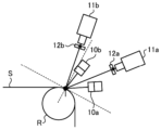
본 실시형태의 표면 검사 장치의 구성예를 도 1 에 나타낸다. 도 1 에 나타내는 바와 같이, 본 실시형태의 표면 검사 장치 (1) 는, 제 1 광학계로서, 금속띠 (S) 에 출사광 (L1) 을 출사하는 제 1 광원부 (2), 제 1 광원부 (2) 로부터의 출사광 (L1) 에 의한 금속띠 (S) 의 정반사광 (L2) 을 촬상하는 제 1 촬상부 (3), 및 제 1 광원부 (2) 로부터의 출사광 (L1) 의 파장 성분을 선택적으로 투과하는 제 1 광학 필터부 (3a) 를 구비하고 있다. 또, 본 실시형태의 표면 검사 장치 (1) 는, 제 2 광학계로서, 금속띠 (S) 에 출사광 (L3) 을 출사하는 제 2 광원부 (4), 제 2 광원부 (4) 로부터의 출사광 (L3) 에 의한 금속띠 (S) 의 난반사광 (L4) 을 촬상하는 제 2 촬상부 (5), 및 제 2 광원부 (4) 로부터의 출사광 (L3) 의 파장 성분을 선택적으로 투과하는 제 2 광학 필터부 (5a) 를 구비하고 있다. 또, 제 1 광원부 (2) 의 출사광 (L1) 과 제 2 광원부 (4) 의 출사광 (L3) 은, 상이한 파장대에서 선택된 광이며, 제 1 광원부 (2) 로부터의 출사광 (L1) 과 제 2 광원부 (4) 로부터 출사광 (L3) 은 금속띠 (S) 의 표면의 동일 지점 (점 P) 에 동시에 조사된다. 또한, 표면 검사 장치 (1) 는, 제 1 광학 필터부 (3a) 및 제 2 광학 필터부 (5a) 를 구비하고 있지 않아도 된다.An example of the configuration of the surface inspection device of the present embodiment is shown in FIG. 1 . As shown in FIG. 1 , the
여기서, 제 1 광학계에 있어서는, 제 1 광원부 (2) 로부터의 출사광 (L1) 이 금속띠 (S) 의 표면에서 반사한 정반사광 (L2) 을 제 1 촬상부 (3) 에 의해 촬상한다. 제 1 광학계는, 금속띠 (S) 의 요철상 결함을 검출하는 데에 적합하다. 이것은, 도 2 에 나타내는 바와 같이, 금속띠 (S) 의 표면에 요철상 결함이 존재하는 경우, 요철면에 의해 정반사광 (L2) 의 광로에 변화가 생기기 때문에, 플랫면과 비교하여 제 1 촬상부 (3) 가 촬상하는 정반사광 (L2) 의 강도가 저하한다, 라는 특성을 이용할 수 있기 때문이다. 한편, 제 2 광학계에 있어서는, 제 2 광원부 (4) 로부터의 출사광 (L3) 이 금속띠 (S) 의 표면에서 반사할 때의 난반사광 (L4) 을 제 2 촬상부 (5) 에 의해 촬상한다. 제 2 광학계는, 금속띠 (S) 의 무늬상 결함을 검출하는 데에 적합하다. 무늬상 결함에는 큰 요철이 형성되어 있지 않기 때문에, 정반사광의 변화는 관찰 스케일과 비교하여 매우 작아, 정반사광을 촬상하고 있어도 수광 강도의 변화가 생기기 어려워, 감도가 높은 검출이 가능하지 않은 경우가 있기 때문이다. 또, 무늬상 결함은, 광의 파장대에 가까운 크기의 미세한 요철에 의해 구성되어 있는 경우가 있어, 광의 파장대에 가까운 크기의 요철에 의한 산란광을 검출함으로써 무늬상 결함의 검출 감도가 향상되기 때문이다.Here, in the first optical system, the
본 실시형태에서는, 제 1 광원부 (2) 의 출사광 (L1) 및 제 2 광원부 (4) 의 출사광 (L3) 으로서, 상이한 파장대에서 선택된 광을 사용한다. 또한, 제 1 촬상부 (3) 에는 제 1 광원부 (2) 로부터의 출사광 (L1) 의 파장 성분을 선택적으로 투과하는 제 1 광학 필터부 (3a) 가 형성되고, 제 2 촬상부 (5) 에는 제 2 광원부 (4) 로부터의 출사광 (L3) 의 파장 성분을 선택적으로 투과하는 제 2 광학 필터부 (5a) 가 형성되어 있다. 이로써, 제 1 광원부 (2) 로부터의 출사광 (L1) 의 정반사광 (L2) 만을 제 1 촬상부 (3) 에서 촬상하고, 제 2 광원부 (4) 로부터의 출사광 (L3) 의 난반사광 (L4) 만을 제 2 촬상부 (5) 에서 촬상할 수 있다. 상이한 파장대에서 선택된 광을 각각의 촬상부에서 선택하여 각각의 반사 강도를 평가하기 위해서이다. 이로써, 제 1 광학계에 의해 요철상 결함을, 제 2 광학계에 의해 무늬상 결함을 각각 검출할 수 있다. 또, 각각의 표면 결함을 전용의 광학계에 의해 검출하는 구성이기 때문에, 각각의 표면 결함에 대한 검출 감도가 향상된다.In this embodiment, as the outgoing light L1 of the first
또한, 본 실시형태에서는, 제 1 광원부 (2) 로부터의 출사광 (L1) 과 제 2 광원부 (4) 로부터의 출사광 (L3) 은 금속띠 (S) 의 표면의 동일 지점에 동시에 조사된다. 상기 서술한 바와 같이, 제 1 광학계에 의해 검출할 수 있는 표면 결함과 제 2 광학계에 의해 검출할 수 있는 표면 결함은 상이한 광의 반사 특성을 갖는 결함이며, 제 1 광학계에 의한 표면 결함의 검출과 제 2 광학계에 의한 표면 결함의 검출은 독립적으로 구성할 수도 있다. 그러나, 그들을 상이한 위치에 설치하면, 각각에서 검출한 표면 결함이 금속띠의 어느 위치에서 발생하고 있는지를 특정하는 것이 곤란해진다.Further, in this embodiment, the outgoing light L1 from the first
본 실시형태에 의하면, 제 1 광원부 (2) 로부터의 출사광 (L1) 과 제 2 광원부 (4) 로부터 출사광 (L3) 은, 금속띠 (S) 의 표면의 동일 지점에 동시에 조사된다. 이로써, 제 1 촬상부 (3) 에 의한 검출 결과와 제 2 촬상부 (5) 에 의한 검출 결과를 직접적으로 대비시킴으로써, 검출한 표면 결함이 어느 종류의 표면 결함에 속하는지를 판별할 수 있다. 예를 들어, 제 1 촬상부 (3) 에 의한 화상에서는 표면 결함이 인식되지 않고, 제 2 촬상부 (5) 에 의한 화상에 기초하여 표면 결함이 인식되는 경우에는, 검출한 표면 결함을 무늬상 결함으로 분류할 수 있다. 또한, 요철상 결함과 무늬상 결함의 특징을 겸비한 표면 결함에 대해, 제 1 촬상부 (3) 에 의한 화상과 제 2 촬상부 (5) 에 의한 화상을 비교하고, 어느 쪽에 가까운 특징을 갖는 표면 결함인지를 판별하는 것이 가능해진다.According to this embodiment, the outgoing light L1 from the first
이에 대하여, 제 1 광학계와 제 2 광학계를 독립적으로 (다른 위치에) 배치한 경우에는, 제 1 광학계에 의해 검출한 결함 정보와 그 검출한 금속띠 (S) 상의 위치 정보의 결부를 실시하고, 또한 제 2 광학계에 의해 검출한 결함 정보와 그 검출한 금속띠 (S) 상의 위치 정보의 결부를 실시할 필요가 생긴다. 이 경우, 금속띠 (S) 에 검출된 표면 결함의 종류를 판별하고자 하면, 금속띠 (S) 상의 위치 정보에 기초하여 제 1 광학계에 의해 검출한 결함 정보와 제 2 광학계에 의해 검출한 결함 정보를 대비시키는 공정이 필요해진다. 이와 같은 금속띠 (S) 상의 위치 정보에 근거하는 결함 정보의 대비 처리를 예를 들어 고속으로 주행하는 금속띠 (S) 표면의 전체면에 대해 실시하는 경우, 고도의 계산기 능력과 속도 측정 성능이 필요로 되어, 표면 검사 장치 전체적으로 고가가 되어 버린다. 또, 이와 같은 금속띠 (S) 상의 위치 정보에 근거하는 결함 정보의 대비 처리를 실행함으로써, 결함 검출을 신속하게 실시할 수 없다는 문제가 생긴다.In contrast, when the first optical system and the second optical system are arranged independently (at different positions), the defect information detected by the first optical system and the positional information on the metal strip S detected are combined with each other, Further, it is necessary to associate the defect information detected by the second optical system with the detected positional information on the metal strip S. In this case, to determine the type of surface defect detected on the metal strip (S), the defect information detected by the first optical system and the defect information detected by the second optical system based on the positional information on the metal strip (S) A process of contrasting is required. When such contrast processing of defect information based on positional information on the metal strip S is performed, for example, on the entire surface of the metal strip S traveling at high speed, high-level calculation capability and speed measurement performance are required. It becomes necessary and becomes expensive as a whole surface inspection apparatus. In addition, by performing contrast processing of defect information based on the positional information on the metal strip S, a problem arises that defect detection cannot be carried out quickly.
이에 대하여, 본 실시형태에서는, 상이한 파장의 광원과, 그것에 대응한 광학 필터 및 각각의 광의 촬상이 가능한 촬상부로 구성되는 광학계를, 동일 지점에 배치함으로써, 표면 결함의 종류를 순시에 판별하는 것이 가능해진다. 또, 각각의 광학계를 별도 배치하는 것보다 장치 전체를 컴팩트하게 구성할 수 있어, 표면 결함 검출을 실시하는 설치 스페이스의 제약이 완화된다.On the other hand, in the present embodiment, by arranging an optical system composed of light sources of different wavelengths, corresponding optical filters, and an imaging unit capable of capturing images of each light, at the same point, it is possible to instantly determine the type of surface defect. It happens. In addition, rather than disposing each optical system separately, the entire apparatus can be configured compactly, and restrictions on the installation space for surface defect detection are alleviated.
〔광학계의 배치〕[Arrangement of optical system]
본 실시형태에서는, 제 1 촬상부 (3) 는, 제 1 광원부 (2) 로부터의 출사광 (L1) 에 의한 금속띠 (S) 의 정반사광 (L2) 을 촬상하는 배치를 취한다. 도 1 에 있어서, 금속띠 (S) 의 법선 (L) 에 대한 제 1 광원부 (2) 의 광축의 각도를 α0, 제 1 촬상부 (3) 의 광축의 각도를 α1 로 하면, 제 1 촬상부 (3) 는, 각도 α0 과 각도 α1 이 대략 동일해지도록 배치된다. 단, 그 차이는 0 인 것이 바람직하지만, 대략 0.5°이내이면 충분한 강도의 정반사광을 수광할 수 있다.In this embodiment, the
한편, 제 2 촬상부 (5) 는, 제 2 광원부 (4) 로부터의 출사광 (L3) 에 의한 금속띠 (S) 의 난반사광 (L4) 을 촬상하는 배치를 취한다. 금속띠 (S) 의 법선 (L) 에 대한 제 2 광원부 (4) 의 광축의 각도를 β0, 제 2 촬상부 (5) 의 광축의 각도를 β1 로 하면, 난반사광 (L4) 을 촬상하기 위해서 제 2 촬상부 (5) 는 각도 β0 과 각도 β1 이 동일하게 되지 않도록 배치된다. 또한, 도 1 에 나타내는 예에서는, 각도 β0 이 각도 β1 보다 커지도록 제 2 촬상부 (5) 는 배치되어 있지만, 제 2 촬상부 (5) 에서는 난반사광 (L4) 을 촬상하면 되고, 각도 β1 이 각도 β0 보다 커도 상관없다. 단, 정반사광을 수광하지 않도록 하기 위해서, 정반사광의 광로축에 대해 15°이상의 차를 갖는 배치가 바람직하다. 여기서, 도 1 에 있어서, 금속띠 (S) 상의 임의의 조사점 (P) 에 대해, 그 조사점 (P) 에서 반사하는 제 1 광원부 (2) 로부터의 출사광 (L1) 과, 정반사에 의해 제 1 촬상부 (3) 를 향하는 정반사광 (L2) 에 의해 구성되는 평면에 대한 법선 벡터가, 제 2 광원부 (4) 로부터 조사점 (P) 을 향하는 출사광 (L3) 의 방향과 수직의 관계에 있는 것으로 한다.On the other hand, the second
〔광원부〕[Light source part]
본 실시형태에서는, 제 1 광원부 (2) 로부터의 출사광 (L1) 및 제 2 광원부 (4) 로부터의 출사광 (L3) 으로는 상이한 파장대의 광을 사용한다. 상이한 파장대란, 광의 스펙트럼 분포 (분광 분포) 가 서로 상이한 것을 말한다. 스펙트럼 분포의 일부가 중복되어 있어도 되고, 스펙트럼 분포의 피크의 파장이 상이하면 된다. 단, 제 1 광원부 (2) 에 의한 정반사광 (L2) 과 제 2 광원부 (4) 에 의한 난반사광 (L4) 을 제 1 촬상부 (3) 와 제 2 촬상부 (5) 에 의해 각각 분리하여 검출하기 위해서, 스펙트럼 분포의 피크 파장은 적어도 50 ㎚ 이상 떨어져 있는 것이 바람직하다. 보다 바람직하게는 100 ㎚ 이상이다. 이것은, 금속띠 (S) 의 동일 지점에 동시에 조사되고, 반사한 광을 분리하여 촬상하기 위해서이며, 제 1 광원부 (2) 로부터의 정반사광 (L2) 과 제 2 광원부 (4) 로부터의 난반사광 (L4) 을 분리하여 촬상하기 쉽기 때문이다.In this embodiment, as the outgoing light L1 from the first
또한, 가시광을 광원부에 사용하는 경우에는, 자색 (파장역이 380 ∼ 430 ㎚ 의 광), 남색 (파장역이 430 ∼ 460 ㎚ 의 광), 청색 (파장역이 460 ∼ 500 ㎚ 의 광), 녹색 (파장역이 500 ∼ 570 ㎚ 의 광), 황색 (파장역이 570 ∼ 590 ㎚ 의 광), 등색 (파장역이 590 ∼ 610 ㎚ 의 광), 적색 (파장역이 610 ∼ 780 ㎚ 의 광) 등, 가시광을 분광하여 얻어지는 색에서 선택한 임의의 파장대의 광을 사용할 수 있다.In addition, when visible light is used for the light source unit, purple (light having a wavelength range of 380 to 430 nm), indigo (light having a wavelength range of 430 to 460 nm), blue (light having a wavelength range of 460 to 500 nm), Green (light with a wavelength range of 500 to 570 nm), yellow (light with a wavelength range from 570 to 590 nm), orange (light with a wavelength range from 590 to 610 nm), red (light with a wavelength range from 610 to 780 nm) ), etc., light of an arbitrary wavelength range selected from colors obtained by spectroscopy of visible light can be used.
또, 제 1 광원부 (2) 와 제 2 광원부 (4) 로부터의 출사광 (L1, L3) 으로서, 가시광뿐만 아니라, 적외선, 자외선의 파장대에서 선택한 임의의 광을 사용해도 된다. 그러한 파장대의 광을 촬상할 수 있는 촬상부를 구비하고 있으면 된다.In addition, as the emitted light (L1, L3) from the first
여기서, 제 1 광원부 (2) 로부터의 출사광 (L1) 은, 제 2 광원부 (4) 로부터의 출사광 (L3) 보다, 장파장의 파장대에서 선택된 광인 것이 바람직하다. 금속띠의 요철상 결함은, 무늬상 결함에 비해 요철의 기복과 요철의 피치가 크기 때문에, 장파장의 광의 산란이 커져, 요철상 결함의 검출 감도가 향상되기 때문이다. 또, 무늬상 결함은 요철의 기복이 작기 때문에, 단파장광일수록 난반사가 현저하게 되어, 무늬상 결함의 검출 감도가 향상되기 때문이다.Here, it is preferable that the light emitted from the first light source unit 2 (L1) is selected from the wavelength range of a longer wavelength than the light emitted from the second light source unit (4) (L3). Concavo-convex defects on a metal strip have larger undulations and pitches than pattern-like defects, so scattering of long-wavelength light is increased, and detection sensitivity of concavo-convex defects is improved. In addition, since pattern-like defects have small unevenness, irregular reflection becomes more remarkable as light of a shorter wavelength is used, and the detection sensitivity of pattern-like defects is improved.
또한, 제 1 광원부 (2) 로부터의 출사광 (L1) 으로서, 난색의 파장대에서 선택된 광을 사용하는 것이 바람직하다. 또, 제 2 광원부 (4) 로부터의 출사광 (L3) 으로서, 한색의 파장대에서 선택된 광을 사용하는 것이 바람직하다. 여기서, 「난색」이란, 색을 심리적 효과에 따라 분류한 호칭이며, 가시광 중에서 따뜻한 느낌을 주는 색을 가리킨다. 구체적으로는, 적자, 적, 등 (주황), 황의 색으로서 관찰되는 광이며, 여기서는 피크 파장이 570 ∼ 780 ㎚ 의 범위에 있고, 535 ㎚ 이하의 파장역의 광이 스펙트럼 분포 전체에 대해 10 % 미만인 광으로 한다. 한편, 「한색」이란, 가시광 중에서 추운 느낌을 주는 색을 가리킨다. 구체적으로는, 청록, 청, 청자의 색으로서 관찰되는 광이며, 여기서는 피크 파장이 380 ∼ 500 ㎚ 의 범위에 있고, 535 ㎚ 이상의 파장역의 광이 스펙트럼 분포 전체에 대해 10 % 미만인 광으로 한다. 가시광을 사용함으로써, 염가의 장치 구성으로 표면 결함 장치를 구성할 수 있기 때문이다. 또, 가시광을 사용함으로써, 금속띠의 표면의 동일 지점에, 그들 광이 조사되는 것을 육안에 의해 확인하기 쉽기 때문이다.Further, as the light emitted from the first light source unit 2 (L1), it is preferable to use light selected from a warm color wavelength band. Further, as the light emitted from the second light source unit 4 (L3), it is preferable to use light selected from a cool color wavelength range. Here, "warm color" is a name for categorizing colors according to psychological effects, and refers to colors giving a warm feeling among visible light. Specifically, it is light observed as red, red, orange (orange), or yellow color, wherein the peak wavelength is in the range of 570 to 780 nm, and light in the wavelength range of 535 nm or less accounts for 10% of the entire spectrum distribution. light that is less than On the other hand, "cold color" refers to a color giving a cold feeling among visible light. Specifically, it is light observed as cyan, blue, or celadon color, and here, the peak wavelength is in the range of 380 to 500 nm, and the light in the wavelength range of 535 nm or more is less than 10% of the entire spectrum distribution. This is because a surface defect device can be configured with an inexpensive device configuration by using visible light. Moreover, it is because it is easy to visually confirm that the light is irradiated to the same spot on the surface of the metal strip by using visible light.
보다 바람직하게는, 제 1 광원부 (2) 로부터의 출사광 (L1) 으로서 적색광을 선택하고, 제 2 광원부 (4) 로부터의 출사광 (L3) 으로서 청색광을 선택한다. 적색광과 청색광은 스펙트럼 분포의 피크가 떨어져 있어 중복이 작기 때문에, 제 1 광원부 (2) 로부터의 정반사광 (L2) 과 제 2 광원부 (4) 로부터의 난반사광 (L4) 을 분리하기 쉽기 때문이다. 또, 적색광은 금속띠의 통상적인 요철상 결함을 산란시키기 쉬운 파장대의 광이며, 청색광은 통상적인 무늬상 결함을 산란시키기 쉬운 파장대의 광이기 때문이다. 이 경우에는, 적색광 및 청색광의 광원으로서, 각각 적색 LED 및 청색 LED 를 바람직하게 사용할 수 있다. 한정된 파장대의 광을 조사하는 광원부로서, 저비용으로 구성할 수 있고, 표면 검사 장치의 소비 전력을 억제할 수 있는 점에서 유리하기 때문이다.More preferably, red light is selected as the outgoing light L1 from the first
또한, 제 1 광원부 (2) 및 제 2 광원부 (4) 의 광원으로는 백색 광원을 사용하는 양태여도 된다. 도 3 에 나타내는 바와 같이, 제 1 광원부 (2) 및 제 2 광원부 (4) 가 금속띠 (S) 에 출사광 (L1, L3) 을 조사하는 경로 상에, 특정한 파장대의 광을 선택적으로 투과시키는 광학 필터 (2a, 4a) 를 배치하는 것이다. 이로써, 각각의 광원부로부터 출사되어 금속띠 (S) 의 표면에 도달하는 시점에서는, 출사광 (L1, L3) 은 서로 상이한 파장대의 광으로 되어 있어, 상기 실시양태와 동일한 효과가 얻어지기 때문이다.Moreover, as a light source of the 1st
〔광학 필터부〕[Optical filter section]
본 실시형태에 있어서의 제 1 촬상부 (3) 에는, 제 1 광원부 (2) 로부터의 출사광 (L1) 의 파장 성분을 선택적으로 투과하는 제 1 광학 필터부 (3a) 가 형성되어 있는 것이 바람직하다. 또, 제 2 촬상부 (5) 에는, 제 2 광원부 (4) 로부터의 출사광 (L3) 의 파장 성분을 선택적으로 투과하는 제 2 광학 필터부 (5a) 가 형성되어 있는 것이 바람직하다. 촬상부에 입사하는 광의 파장을 광학 필터에 의해 한정해 두는 것에 의해, 촬상부 또는 결함 정보 처리부에 있어서 입사광의 분광 처리를 실시할 필요가 없어지기 때문에, 정보 처리를 고속으로 실시할 수 있다. 이로써, 금속띠 (S) 의 반송 속도가 높은 제조 라인에 대해 표면 검사를 실시하는 것이 가능해진다.It is preferable that the first
광학 필터는, 특정한 파장 범위의 광만을 투과하고, 그 이외의 광을 투과하지 않는 광학 소자이다. 광학 필터로는, 흡수식과 반사식 중 어느 것을 적용해도 된다. 각각의 광원부의 출사광의 파장 성분에 대응한 파장의 광만을 투과시키는 밴드 패스 필터가 바람직하다. 단, 제 1 광원부 (2) 로부터의 출사광 (L1) 의 파장과 제 2 광원부 (4) 로부터의 출사광 (L3) 의 파장이 중복되는 측의 성분만을 차단하는 롱 패스 필터 또는 숏 패스 필터를 각각에 적용해도 된다. 즉, 제 1 광원부 (2) 로부터의 출사광 (L1) 의 파장이 제 2 광원부 (4) 로부터의 출사광 (L3) 의 파장보다 긴 경우에는, 제 1 광원부 (2) 로부터의 출사광 (L1) 에는 단파장측을 차단하는 롱 패스 필터를 적용하고, 제 2 광원부 (4) 로부터의 출사광 (L3) 에는 장파장측을 차단하는 숏 패스 필터를 적용해도 된다.An optical filter is an optical element that transmits only light in a specific wavelength range and does not transmit light other than that. As the optical filter, either an absorption type or a reflection type may be applied. A band pass filter that transmits only light of a wavelength corresponding to the wavelength component of light emitted from each light source unit is preferable. However, a long pass filter or a short pass filter that blocks only components on the side where the wavelength of the emitted light L1 from the first
광학 필터의 특성으로서, 각 광원부로부터의 출사광의 스펙트럼 밴드의 중간점 (중심 파장) 을 투과시키는 것을 선택한다. 또, 광학 필터가 투과시키는 스펙트럼 밴드의 밴드폭은, 각 광원부로부터의 출사광의 스펙트럼 분포와 동등 혹은 넓은 것을 사용하는 것이 바람직하다.As the characteristic of the optical filter, one that transmits the midpoint (central wavelength) of the spectral band of light emitted from each light source unit is selected. In addition, it is preferable that the band width of the spectral band transmitted by the optical filter is equal to or wider than the spectrum distribution of light emitted from each light source unit.
도 4 는, 제 1 광원부 (2) 에 적색 LED, 제 2 광원부 (4) 에 청색 LED 를 적용한 경우의, 각각의 출사광을 선택적으로 투과하기 위한 광학 필터부의 특성을 나타낸 예이다. 제 1 광원부 (2) 에 의한 출사광 (L1) 의 스펙트럼 밴드 (A1) 와 제 2 광원부 (4) 에 의한 출사광 (L3) 의 스펙트럼 밴드 (A2) 는 중복이 없는 파장대의 광을 사용하고 있다. 이에 대하여, 제 1 광학 필터부 (3a) 가 투과시키는 스펙트럼 밴드 (B1) 와 제 2 광학 필터부 (5a) 가 투과시키는 스펙트럼 밴드 (B2) 는, 출사광의 스펙트럼 밴드를 포함하고 있다. 또, 광학 필터가 투과시키는 밴드폭은, 대응하는 광원의 스펙트럼 분포보다 넓은 범위의 파장을 투과시키는 특성을 갖는다. 이때, 광원부로부터의 출사광의 스펙트럼 분포의 피크와, 광학 필터부의 중심 파장은 반드시 일치하고 있을 필요는 없다. 광원의 스펙트럼 분포를 커버할 수 있는 정도로 넓은 범위의 파장을 선택적으로 투과시키는 특성이면 된다. 광원의 스펙트럼 분포를 커버하는 반사광을 투과시킴으로써 촬상부에서의 수광량이 증가하여, 검출 감도가 향상되기 때문이다. 단, 광원부의 스펙트럼 분포보다 광학 필터가 투과시키는 밴드폭이 좁은 것을 선택해도 상관없다. 촬상부에서 수광하는 광의 파장을 한정함으로써, 결함을 판별하기 쉽다는 효과가 얻어진다.4 is an example showing the characteristics of an optical filter unit for selectively transmitting each emitted light when a red LED is applied to the first
한편, 본 실시형태에 있어서의 제 1 광학 필터부 (3a) 및 제 2 광학 필터부 (5a) 는, 출사광의 파장 성분을 선택적으로 투과시키는 기능을 구비한 것이면, 다른 광학 부품에 의해 대체할 수도 있다. 예를 들어, 광원부에 가시광을 사용하는 경우에, 광학 필터부로서 프리즘을 사용하여 가시광을 분광하고, 각각의 광원부의 출사광에 대응한 분광 후의 광만을 촬상부에 유도하도록 해도 된다.On the other hand, the first
또한, 제 1 촬상부 및 제 2 촬상부로서, 고체 촬상 소자 (CCD, CMOS) 를 사용한 컬러 카메라를 적용하는 경우에는, 상기 광학 필터부가 촬상부와 일체화된 장치 구성이 된다. 고체 촬상 소자에 의한 색분해를 위한 방식으로는 다판 방식과 단판 방식이 있다. 다판 방식에서는, 색분해 프리즘으로 화상이 색분해되고, 색분해된 화상이 3 개 또는 4 개의 고체 촬상 장치에 의해 전기 신호로 변환되어 색신호가 얻어진다. 한편, 단판 방식에서는, 고체 촬상 장치에 형성된 3 색 또는 4 색의 온 칩 컬러 필터로 화상이 색분해되고, 색분해된 화상이 하나의 고체 촬상 장치에 의해 전기 신호로 변환되어 색신호가 얻어진다. 이때, 제 1 광원부 (2) 로부터의 출사광 (L1) 으로서 적색광, 제 2 광원부 (4) 로부터의 출사광 (L3) 으로서 청색광을 사용한 경우에, 다판 방식에 있어서는, 색분해 프리즘으로 화상을 색분해하여 적색광 또는 청색광으로 분광하는 부분이 상기 광학 필터부에 대응하고, 고체 촬상 장치에 의해 적색 또는 청색의 전기 신호로 변환하는 부분이 촬상부에 대응하게 된다. 또, 단판 방식에서는, 온 칩 컬러 필터로 화상이 적색 또는 청색으로 색분해되는 부분이 광학 필터부에 대응하고, 색분해된 화상이 하나의 고체 촬상 장치에 의해 전기 신호로 변환되어 적색 또는 청색의 색신호를 얻는 부분이 촬상부에 대응한다. 또한, 마이크로 분광 소자를 사용하여 광의 회절 현상을 이용한 이미지 센서를 사용하는 경우에도, 회석에 의해 색분리가 실시되는 것이며, 광학 필터부에 대응한다. 최근의 반도체 기술의 진보에 의해, 광학 필터부와 촬상부의 기능을 구비한, 고속 처리가 가능한 기기가 실용화되어 온 점에서, 고속으로 금속띠를 반송하는 제조 라인에 대해서도 컬러 카메라를 사용한 결함 검출 장치를 실현할 수 있도록 되었다.In addition, when a color camera using a solid-state image sensor (CCD, CMOS) is used as the first and second imaging units, the optical filter unit and the imaging unit are integrated into a device configuration. Methods for color separation by a solid-state imaging device include a multi-plate method and a single-plate method. In the multi-plate method, an image is color-separated by a color-separation prism, and the color-separated image is converted into electrical signals by three or four solid-state imaging devices to obtain color signals. On the other hand, in the single plate method, an image is color-separated by a three or four-color on-chip color filter formed in a solid-state imaging device, and the color-separated image is converted into an electrical signal by one solid-state imaging device to obtain a color signal. At this time, when red light is used as the light L1 emitted from the first
〔촬상부〕[Imaging unit]
본 실시형태에서는, 표면 검사 장치 (1) 는, 제 1 광원부 (2) 로부터의 출사광 (L1) 에 의한 금속띠 (S) 의 정반사광 (L2) 을 촬상하는 제 1 촬상부 (3) 와, 제 2 광원부 (4) 로부터의 출사광 (L3) 에 의한 금속띠 (S) 의 난반사광 (L4) 을 촬상하는 제 2 촬상부 (5) 를 각각 구비하고 있다. 2 개의 촬상부를 개별적으로 배치함으로써, 요철상 결함과 무늬상 결함과 같이 상이한 종류의 표면 결함의 각각에 대한 검출 감도를 향상시킬 수 있다. 또, 2 개의 촬상부에 의해 촬상된 화상을 대비함으로써, 검출된 표면 결함이 어느 종류의 결함에 속하는지를 판별할 수 있다.In the present embodiment, the
여기서, 제 1 촬상부 (3) 와 제 2 촬상부 (5) 로는, 정반사광 (L2) 또는 난반사광 (L4) 을 수광하고, 그 화상을 동영상 또는 정지영상으로서 촬영할 수 있는 카메라를 사용한다. 금속띠 (S) 가 정지한 상태 또는 반송 속도가 낮은 상태로 반송하면서 표면 결함의 검사를 실시하는 경우에는, 정지영상을 촬영하는 카메라를 사용해도 된다. 단, 통상적인 금속띠 (S) 의 제조 라인과 같이 비교적 높은 속도 (예를 들어, 10 ∼ 500 m/min 정도) 로 반송하면서 표면 결함의 검사를 실시하는 경우에는, 동영상을 촬영하는 비디오 카메라를 사용하는 것이 바람직하다. 비디오 카메라의 셔터 스피드는, 고속으로 반송되는 금속띠에 대응하기 위해서 빠른 속도의 것이 바람직하지만, 대략 60 Hz 정도의 것을 사용하면 된다. 단, 금속띠의 반송 속도가 500 ∼ 2000 m/min 정도인 조건에서는, 하이 스피드 카메라 (180 Hz 정도) 를 적용해도 된다. 비디오 카메라를 선정할 때에는, 금속띠의 반송 속도와, 검출한 표면 결함을 판별하기 위한 처리 시간이나 검출한 결함 정보를 보존하기 위한 기억 매체의 용량이나 처리 능력을 고려하여 적절히 결정하면 된다.Here, as the
또, 촬상부에 사용하는 카메라로는 디지털 카메라가 바람직하다. 제 1 촬상부 (3) 와 제 2 촬상부 (5) 에서 촬상한 화상이 디지털 화상이면, 양자를 중첩하는 것이 용이하여, 검출한 표면 결함의 특징을 보다 상세하게 파악할 수 있기 때문이다. 또한, 촬상부가 컬러 디지털 카메라에 의해 구성되는 경우에, 촬상된 컬러 화상을 색분해하여, 제 1 광원부 (2) 및 제 2 광원부 (4) 의 파장의 수광 성분을 추출해도 된다.Moreover, a digital camera is preferable as a camera used for the imaging unit. This is because, if the images captured by the
한편, 본 실시형태에서는, 표면 검사 장치 (1) 는, 제 1 광학 필터부 (3a) 및 제 2 광학 필터부 (5a) 를 구비하기 때문에, 제 1 촬상부 (3) 와 제 2 촬상부 (5) 에는 모노크롬 디지털 카메라를 적용할 수 있다. 제 1 광학 필터부 (3a) 및 제 2 광학 필터부 (5a) 에 의해 광원부에 대응한 파장대의 광이 투과되므로, 촬상부에서는 수광하는 광의 강도 정보가 얻어지면, 요철상 결함 및 무늬상 결함의 각각을 인식할 수 있기 때문이다. 모노크롬 디지털 카메라의 셔터 스피드는 빠르기 때문에, 고속으로의 표면 결함 검출이 가능하어, 표면 결함 검출의 설비 비용을 억제할 수 있다.On the other hand, in this embodiment, since the
〔라인 광원〕[Line light source]
본 실시형태에서는, 제 1 광원부 (2) 와 제 2 광원부 (4) 는, 금속띠 (S) 의 표면에 라인상으로 광을 조사하는 라인상 광원인 것이 바람직하다. 또, 제 1 광원부 (2) 와 제 2 광원부 (4) 의 라인상 광원은, 금속띠 (S) 의 표면에 조사하는 경우, 금속띠 (S) 의 반송 방향에 대해 수직 방향으로 조사하도록 배치하는 것이 바람직하다. 단, 금속띠 (S) 의 반송 방향에 대해 70 ∼ 120°의 각도에 있으면, 반드시 수직 (90°) 이 아니어도 된다. 금속띠 (S) 를 반송하면서 표면 결함의 검출을 실시하는 경우에, 금속띠 (S) 의 폭 방향으로 라인상의 광을 조사하고, 그 반사광을 디지털 카메라로 검출함으로써, 금속띠 (S) 의 폭 방향의 임의의 위치에 있는 표면 결함 검출이 가능해진다. 또, 디지털 카메라의 셔터 스피드에 따른 화상을 취득함으로써, 금속띠 (S) 의 길이 방향으로 연속적인 면화상을 생성하는 것이 가능해져, 금속띠 (S) 의 전체면에 있어서의 표면 결함의 검사가 가능해지기 때문이다.In this embodiment, it is preferable that the 1st
라인상의 광이란, 선광원으로 한정되지 않고, 금속띠 (S) 에 대해 장방형의 범위에서 광을 조사하는 광원이고, 1 변의 방향의 조사 범위가 타변의 조사 범위보다 10 배 이상 긴 광원을 말한다. 본 실시형태에서는, 장방형의 조사 범위의 장변의 방향을 적어도 금속띠 (S) 의 폭 방향보다 긴 범위를 조사하는 것이 바람직하다. 단, 반드시 금속띠 (S) 의 폭 (대략 400 ∼ 2000 ㎜) 을 하나의 광원으로 조사할 필요는 없다. 복수의 광원을 금속띠 (S) 의 폭 방향으로 배치하여 금속띠 (S) 에 광을 조사하여도 된다.Line-shaped light is not limited to a linear light source, but refers to a light source that irradiates light in a rectangular range to the metal strip S, and the irradiation range in one side direction is 10 times or more longer than the other side irradiation range. In this embodiment, it is preferable to irradiate a range longer than the width direction of the metal strip S in the direction of the long side of the rectangular irradiation range. However, it is not always necessary to irradiate the width of the metal strip S (approximately 400 to 2000 mm) with one light source. Light may be irradiated to the metal strip S by arranging a plurality of light sources in the width direction of the metal strip S.
또, 제 1 광원부 (2) 와 제 2 광원부 (4) 로부터의 출사광은, 금속띠 (S) 의 표면의 동일 지점에 조사하는 것이지만, 제 1 광원부 (2) 와 제 2 광원부 (4) 의 금속띠 (S) 의 폭 방향의 범위가 상이한 등, 일부에 조사광이 겹치지 않는 영역이 있어도 상관없다. 조사광이 겹치는 영역에서는, 상기 양태로의 표면 결함 검사가 가능하기 때문이다. 이것은, 조사광의 단변측의 영역의 일부에, 조사광이 겹치지 않는 영역이 있는 경우도 동일하다.In addition, the outgoing light from the first
또한, 라인 광원을 사용하는 경우에는, 제 1 촬상부 (3) 및 제 2 촬상부 (5) 에는 라인 스캔 카메라 또는 에어리어 카메라를 적용할 수 있다. 라인 스캔 카메라는 선상의 광을 촬상하는 데에 적합하고, 장방형의 조사 영역이 되는 경우에는 에어리어 카메라가 바람직하다.In the case of using a line light source, a line scan camera or an area camera can be applied to the
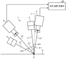
라인상 광원을 사용한 경우의 표면 검사 장치의 구성예를 도 5 에 나타낸다. 도 5 에 나타내는 구성예는, 금속띠 (S) 의 처리 공정에 있어서, 금속띠 (S) 를 반송시킬 때에 감기는 롤 (R) 을 이용한 것이다. 도 5 에 있어서, 부호 10a 는 단파장의 단색 광원, 부호 10b 는 장파장의 단색 광원, 부호 11a 는 암시야 (DF) 라인 스캔 카메라, 부호 11b 는 명시야 (BF) 라인 스캔 카메라, 부호 12a 는 단파장 필터, 부호 12b 는 장파장 필터를 나타내고 있다. 금속띠 (S) 를 롤 (R) 에 감음으로써, 반송 시의 금속띠 (S) 의 요동을 방지할 수 있어, 안정적인 반사광을 얻을 수 있다.An example of the configuration of a surface inspection device in the case of using a linear light source is shown in FIG. 5 . In the configuration example shown in Fig. 5, in the processing step of the metal strip S, a roll R to be wound when conveying the metal strip S is used. 5,
〔광원부와 촬상부의 배치〕[Arrangement of light source unit and imaging unit]
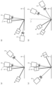
본 실시형태에 있어서의 광원부와 촬상부의 배치에 대해서는, 도 1 에 나타내는 배치 이외에, 도 6 에 나타내는 배치를 적용할 수 있다. 예를 들어 도 6(a) 에 나타내는 바와 같이, 제 2 광원부 (4) 와 제 2 촬상부 (5) 를 금속띠 (S) 의 법선 (L) 에 대해 반대측에 배치할 수 있다. 단, 제 2 촬상부 (5) 는 난반사광을 촬상하는 것이기 때문에, 제 2 광원부 (4) 의 정반사광을 수광하는 위치 (도 1 에 나타내는 각도 β1 이 대략 마이너스 각도 β0 과 동일한 위치) 에는 배치하지 않는다. 또, 제 2 광원부 (4) 로부터의 출사광의 입사각이나 제 2 촬상부 (5) 의 광축의 각도가, 제 1 광원부 (2) 와 제 1 촬상부 (3) 의 각도의 대소 관계도 문제는 되지 않고, 적절히 선택할 수 있다.Regarding the arrangement of the light source unit and the imaging unit in this embodiment, the arrangement shown in FIG. 6 can be applied in addition to the arrangement shown in FIG. 1 . For example, as shown in Fig. 6(a), the second
이때, 제 2 광원부 (4) 에 의한 출사광의 금속띠에 대한 입사각도 β0 은, 제 1 광원부 (2) 에 의한 출사광의 입사각도 α0 보다 크게 하는 것이 바람직하다. 단, 상기와 같이 금속띠 (S) 의 법선 (L) 에 대해 동일한 측에 배치할 필요는 없다. 제 2 광학계에서 검출하는 무늬상 결함은, 출사광의 입사각도 β0 이 클수록, 검출 감도가 향상되고, 정반사광에 의한 노이즈 영향은 입사각도 β0 에 비례하여 감쇠하기 때문이다. 또, 제 1 광원부 (2) 로부터의 정반사광을 제 1 촬상부 (3) 에서 촬상하는 경우에, 제 2 광원부 (4) 로부터의 출사광의 반사광이 제 1 광학 필터부 (3a) 를 향하는 영향도가 경감되어, 표면 결함의 판별이 용이해지기 때문이다.At this time, it is preferable that the angle of incidence β0 of the light emitted from the second
한편, 제 1 광원부 (2) 로부터의 출사광의 입사각도 α0 및 제 1 촬상부 (3) 의 광축이 금속띠 (S) 의 법선 (L) 에 대해 이루는 각도 α1 은, 0°이상 75°이하의 각도가 바람직하다. 제 1 광원부 (2) 로부터의 출사광의 입사각이 커지면, 얕은 입사에 의해 판면에 대한 조사 면적이 넓어지기 때문에, 금속띠 표면의 단위면적당의 반사광량이 저하하여 촬상 조건이 악화되는 것 외에, 금속띠의 진동이나 두께 변동 등의 외란 영향을 받기 쉬워지기 때문이다. 또한, 제 1 광원부 (2) 로부터의 출사광의 입사각은 0°여도 된다. 그 경우에는 광로의 도중에 하프 미러를 배치하고, 돌아오는 정반사광만 광로가 다른 방향이 되도록 하고, 그 광로의 위치에 제 1 촬상부 (3) 를 배치하는 동축 낙사 형태를 채용할 수 있다.On the other hand, the incident angle α0 of the light emitted from the first
또한, 제 2 촬상부 (5) 의 광축은, 금속띠 (S) 의 법선 (L) 에 대해 20°이상 90°미만의 각도인 것이 바람직하다. 제 2 촬상부 (5) 의 광축을 금속띠 (S) 의 법선 (L) 에 대해 20°이상으로 하는 것은, 제 1 광원부 (2) 로부터의 출사광의 입사각도 α0 을 작게 설정하는 경우에, 제 2 광학계의 장치 배치가 용이하게 되기 때문이다. 또, 특히 금속띠 (S) 의 무늬상 결함의 검출 감도가 향상된다는 지견에 근거한다. 또한, 제 2 촬상부 (5) 의 광축과 금속띠 (S) 의 법선 (L) 이 이루는 각도 β1 이 90°가 되는 배치로 하지 않는 것은, 제 2 촬상부 (5) 의 카메라를 매우 높은 정밀도로 설치하지 않으면, 제 2 광원부 (4) 로부터의 난반사광을 수광할 수 없게 되는 경우가 있기 때문이다.In addition, it is preferable that the optical axis of the
금속띠 (S) 가 도금 강판인 경우에는, 제 1 광원부 (2) 로부터의 출사광의 입사각도 α0 및 제 1 촬상부 (3) 의 광축이 금속띠 (S) 의 법선 (L) 에 대해 이루는 각도 α1 은, 0°이상 45°이하가 보다 바람직하다. 또, 제 2 촬상부 (5) 의 광축은, 금속띠 (S) 의 법선 (L) 에 대해 30°이상 90°미만의 각도가 되는 것이 보다 바람직하다. 금속띠 (S) 의 표면에 실시하는 도금의 종류나 피막두께에 따라서는, 제 1 광원부 (2) 로부터의 출사광의 입사각도 α0 을 작게 함으로써 요철상 결함의 검출 감도가 향상되고, 제 2 촬상부 (5) 의 광축을 30°이상으로 함으로써, 무늬상 결함의 검출 감도가 향상되기 때문이다. 예를 들어, 전기 도금 라인에 의해 박막의 도금이 부여되는 금속띠 (S) 에 대해서는, 제 1 광원부 (2) 로부터의 출사광의 입사각도 α0 및 제 1 촬상부 (3) 의 광축이 금속띠 (S) 의 법선 (L) 에 대해 이루는 각도 α1 을 5°이상 20°이하로 설정해도 된다. 또, 제 2 촬상부 (5) 의 광축에 대해서는, 금속띠 (S) 의 법선 (L) 에 대해 45°이상 85°미만의 각도로 해도 된다.When the metal strip S is a plated steel sheet, the incident angle α0 of the light emitted from the first
〔결함 정보 처리부〕[Defect Information Processing Unit]
본 실시형태에서는, 상기와 같은 제 1 광학계와 제 2 광학계를 조합한 장치 구성에 있어서, 제 1 촬상부 (3) 에 의해 촬영된 화상과 제 2 촬상부 (5) 에 의해 촬영된 화상으로부터, 금속띠 (S) 의 표면에서 검출된 결함이 요철상 결함인지 무늬상 결함인지를 화상에 의해 판별할 수 있다. 또한, 표면 검사 장치 (1) 는, 상기 구성에 있어서, 도 7 에 나타내는 바와 같이, 제 1 촬상부 (3) 에 의해 촬상된 화상과 제 2 촬상부 (5) 에 의해 촬상된 화상을 사용하여, 금속띠 (S) 의 표면 결함의 판별을 실시하는 표면 결함 판별부 (20) 를 구비하고 있다.In the present embodiment, in the device configuration combining the first optical system and the second optical system as described above, from the image captured by the
이 경우, 제 1 광원부 (2) 로부터의 출사광 (L1) 과 제 2 광원부 (4) 로부터 출사광 (L3) 은, 금속띠 (S) 의 표면의 동일 지점 (점 P) 에 동시에 조사되어, 제 1 광원부 (2) 로부터의 정반사광 (L2) 을 제 1 촬상부 (3) 에서 촬상함과 함께, 제 2 광원부 (4) 로부터의 난반사광 (L4) 을 제 2 촬상부 (5) 에 의해 촬상한다. 이와 같이 하여 촬영된 화상은, 동시에 금속띠 (S) 의 표면에 조사되었을 때의 화상이며, 그들 화상이 표면 결함 판별부 (20) 로 보내진다.In this case, the outgoing light L1 from the first
표면 결함 판별부 (20) 는, 예를 들어, 워크스테이션이나 퍼스널 컴퓨터 등의 범용 컴퓨터에 의해 구성되어 있다. 표면 결함 판별부 (20) 는, 요철 결함 판정부, 무늬상 결함 판정부, 및 격납부를 가지고 있다. 요철 결함 판정부와 무늬상 결함 판정부는, 예를 들어 CPU 등이고, 격납부에 보존된 컴퓨터 프로그램이나 데이터를 사용하여, 요철 결함 판정부와 무늬상 결함 판정부가 갖는 기능을 실현시키기 위해서 소정의 연산을 실행한다.The surface
요철 결함 판정부 및 무늬상 결함 판정부에 있어서의 처리는, 구체적으로는 이하와 같이 하여 실시할 수 있다. 도 8 은 본 실시형태의 결함 정보 처리의 일례를 나타내는 도면이다. 이것은 광원부에 라인 광원을 사용하고, 라인 스캔 카메라에 의해 금속띠의 폭 방향으로 스캔하여 촬상한 예를 대상으로 하고 있다.The processing in the concavo-convex defect determination unit and pattern-like defect determination unit can be specifically performed as follows. 8 is a diagram showing an example of defect information processing in the present embodiment. This is intended for an example in which a line light source is used for the light source unit and an image is captured by scanning in the width direction of the metal strip with a line scan camera.
본 실시형태의 결함 정보 처리에서는, 먼저, 표면 결함 판별부 (20) 가, 제 1 촬상부 (3) 가 취득한 정반사광 (L2) 의 금속띠의 폭 방향에 대한 스캔 정보와, 제 2 촬상부 (5) 가 취득한 난반사광 (L4) 의 금속띠의 폭 방향에 대한 스캔 정보를 취득한다. 어느 스캔 정보도 도 8(a) 에 나타내는 바와 같은 수광 강도 정보로서 취득된다. 수광 강도 정보란, 촬상부에 의해 취득한 특정한 파장대의 광 강도의 정보이고, 검사 대상인 금속띠의 폭 방향 위치와의 대응 관계가 특정되어 있는 정보를 말한다. 도 8(a) 는, 금속띠의 폭 방향 위치와 강도 (특정한 파장대의 광 강도) 의 관계를 차트 화상으로서 나타낸 것이다. 단, 수광 강도 정보는, 광 강도와 금속띠의 폭 방향 위치의 대응 관계가 특정되어 있으면 되고, 반드시 차트 화상의 형식일 필요는 없다. 한편, 수광 강도 정보가, 광학계의 구성에 수반하는 불가피적인 폭 방향 분포를 갖는 경우 (금속띠에 표면 결함이 없는 상태여도 수광 강도 정보가 폭 방향으로 일정한 분포를 갖는 경우), 표면 결함 판별부 (20) 는, 전처리로서 수광 신호에 쉐이딩 보정을 가함으로써, 광학계의 특성에서 기인하여 촬상부에서 생기는 수광 신호의 오차를 저감한 것을 수광 강도 정보로 해도 된다. 이때, 도 8(a) 에 나타내는 금속띠의 폭에 대응하는 측정 범위 내에 있어서, 수광 강도의 분포가, 각각의 결함에 대응하여 미리 설정되는 상하한의 임계값 (허용 범위) 과 비교된다. 그리고, 수광 강도에 허용 범위 외가 되는 부분이 생긴 경우에, 그 부분은 결함 후보로서 격납부에 기억된다. 여기서는, 이와 같이 하여 생성된 결함 후보에 관한 정보를 결함 후보 정보라고 부른다. 결함 후보 정보는, 수광 강도 정보가 상하한의 임계값을 초과한 금속띠의 폭 방향 위치와, 그 위치에서의 수광 강도의 크기 (예를 들어 임계값과의 편차 등) 가 대응시켜진 정보이다. 결함 후보 정보도 수광 강도 정보와 마찬가지로 차트 화상의 형식으로서 격납부에 기억되어도 된다.In the defect information processing of the present embodiment, first, the surface
다음으로, 표면 결함 판별부 (20) 는, 결함 후보 정보를 금속띠의 길이 방향에 대해 연속적으로 취득하고, 그들을 일정한 거리에서 결합시킨 연속적인 화상 (이차원 화상) 을 취득한다 (도 8(b)). 예를 들어, 촬상부로서 라인 스캔 카메라를 사용한 경우에는, 1 회째의 라인 스캔에 대응하여, 제 1 촬상부 (3) 에 의한 수광 강도 정보와 제 2 촬상부 (5) 에 의한 수광 강도 정보로서 차트 화상이 취득되고, 각각의 차트 화상으로부터 제 1 결함 후보 정보가 생성된다. 다음으로, 금속띠의 반송에 수반하여, 2 회째의 라인 스캔이 실시되면, 제 1 촬상부 (3) 에 의한 수광 강도 정보와 제 2 촬상부 (5) 에 의한 수광 강도 정보로서 차트 화상이 취득되고, 각각의 차트 화상으로부터 제 2 결함 후보 정보가 생성된다. 이와 같이 하여, 라인 스캔이 a1 ∼ aN 까지 실시되면, 제 1 촬상부 (3) 로부터 얻어지는 a1 ∼ aN 까지의 결함 후보 정보와, 제 2 촬상부 (5) 로부터 얻어지는 a1 ∼ aN 까지의 결함 후보 정보가 생성된다. 도 8(b) 의 좌측에 나타내는 도면은, 제 1 촬상부 (3) 에 의해 얻어지는 결함 후보 정보로서, a1 ∼ aN 까지의 결함 후보 정보를 모식적으로 나타낸 것이다. 그리고, 이들 결함 후보 정보는, 도 8(b) 의 우측에 나타내는 도면과 같이 하여 이차원 화상으로 변환된다. 즉, 1 개의 결함 후보 정보의 폭 방향 위치가, 이차원 화상의 폭 방향으로 분할된 화소에 할당되고, 미리 설정되는 수광 강도의 구분에 따라, 각각의 폭 방향 위치에 있어서의 수광 강도의 크기가 명도나 색 등의 정보로 변환되어, 이차원 화상의 화소에 할당된다. 그리고, a1 ∼ aN 까지의 결함 후보 정보가, 이차원 화상의 세로 방향의 화소에 순차 할당됨으로써, 도 8(b) 의 우측에 예시하는 이차원 화상이 생성된다. 동일하게 하여, 제 2 촬상부 (5) 로부터 취득한 결함 후보 정보에 근거하는 이차원 화상도 생성되고, 어느 이차원 화상도 격납부에 기억된다. 또한, 촬상부로서 에어리어 카메라를 사용하는 경우에는, 길이 방향으로 연속하여 촬상된 화상의 중복부를 제거하는 화상 처리를 실시함으로써, 도 8(b) 에 나타내는 이차원 화상과 동일한 이차원 화상을 생성할 수 있다. 또한, 이차원 화상을 생성하는 경우에는, 수광 신호의 강도 (평균값으로부터의 편차 강도) 에 따라, 265 단계의 명도를 할당함으로써, 농담이 있는 이차원 화상으로 하는 것이 바람직하다. 결함 후보 정보에 관한 이차원 화상은, 금속띠를 반송 중에 수시 생성해도 되고, 격납부에 축적된 수광 강도 정보를 사용하여 오프 라인으로 생성해도 된다.Next, the surface
다음으로, 표면 결함 판별부 (20) 는, 결함 후보로서 식별한 부분의 이차원 화상 (결함 후보 정보에 관한 이차원 화상) 을 참조하여, 그 주변에 있어서 명도 분포의 불균일이 생겨 있는 영역을 특정하고, 그 부분이 결함인지 여부를 판정한다. 이때, 명도가 불균일해지는 영역의 넓어짐 (유사한 명도를 나타내는 픽셀의 범위) 은 결함의 크기에 대응한다. 또, 명도의 톤의 차이 (백그라운드로부터의 차) 가, 결함의 정도 (중도) 와 대응한다. 이상의 결함 판정의 처리 플로는, 요철 결함 판정부 (제 1 촬상부로부터 취득한 수광 강도 정보에 근거하는 결함 판정부) 및 무늬상 결함 판정부 (제 2 촬상부로부터 취득한 수광 강도 정보에 근거하는 결함 판정부) 의 각각에 대해 실행된다. 단, 도 8(a) 에 나타내는 상하한의 임계값에 대해서는, 각각의 결함에 대응하여, 육안에 의해 결함이라고 인식되는 것을 검출할 수 있도록 설정하면 된다.Next, the surface
또, 표면 결함 판별부 (20) 는, 이상과 같이 하여 취득되는 이차원 화상의 명도의 분포에 대응하여, 미리 결함의 종류에 따른 화상의 특징량을 데이터베이스에 결함 데이터베이스로서 보존하고 있어도 된다 (도 8(c)). 실제의 조업에 있어서 검출된 결함의 특징을 이차원 화상의 특징량과 대응시켜 둠으로써, 검출된 이차원 화상으로부터 결함 데이터베이스를 참조하는 것에 의해, 결함의 명칭을 특정할 수 있다. 또한, 결함마다, 결함의 정도 (중도) 와 이차원 화상의 특징량을 대응시킨 결함 데이터베이스로 해 둠으로써, 검출되는 결함의 정도 (중도) 를 자동 판정할 수 있다. 또한, 결함 명칭의 판별과 중도의 판정은, 도 8(b) 에 나타내는 바와 같은 이차원 화상을 취득할 수 있으면, 각종의 방법에 의해 판정이 가능하다. 예를 들어, 화상을 입력으로 하고, 결함 명칭과 그 중도를 출력으로 하는 기계 학습 모델을 딥 러닝이나 합성곱 뉴럴 네트워크 등의 수법에 의해 생성해 둠으로써, 이차원 화상으로부터 결함의 판별과 중도의 판정을 실시할 수 있다.In addition, the surface
이때, 어느 것의 결함으로 판정된 경우에는, 그 표면 결함의 정도 (중도) 와 종류의 판정 정보와 함께, 그 결함이 검출된 금속띠 상의 위치 정보가 결부되어 격납부에 축적된다. 또, 조작실의 화면 정보로서, 결함 정보를 출력하는 등에 의해, 결함 정보에 근거하는 생산 공정의 변경이나, 금속띠의 품질 확보에 필요한 대응을 조작자에게 촉구할 수 있다.At this time, when one of the defects is determined, information about the degree (severity) and type of the surface defect is determined, together with information on the location on the metal strip where the defect is detected, and stored in the storage unit. In addition, by outputting defect information as screen information in the operation room, for example, it is possible to prompt the operator to change the production process based on the defect information or to take measures necessary to secure the quality of the metal belt.
또한, 표면 결함 판별부 (20) 는, 상기에 있어서, 결함 후보 정보의 생성 및 결함 후보 정보에 관한 이차원 화상의 생성을 실시하는 표면 결함 정보 검출부와, 결함 후보 정보에 관한 이차원 화상에 근거하여 결함인지 여부를 판정하는 표면 결함 정보 판별부 (요철 결함 판정부 및 무늬상 결함 판정부) 의 2 개로 하드웨어 구성을 구분해도 된다. 전자는, 온라인 처리를 실행하기 위해서 고속 처리가 필요하고, 후자는 오프 라인 처리를 실행하는 것이기 때문에, 그들은 요구되는 하드웨어 성능이 상이하기 때문이다. 또한, 표면 결함 정보 검출부를 복수의 제조 라인에 설치하고, 표면 결함 정보 판별부는 서버상에 구성해도 된다. 복수의 제조 라인으로부터 취득하는 결함 후보 정보에 관한 이차원 화상에 기초하여, 서버상의 표면 결함 정보 판별부가 표면 결함의 판별을 일괄적으로 실시해도 된다. 상이한 제조 라인에 대해, 통일된 기준하에서 결함 판별을 실시하는 것이 가능해져, 결함 판별의 편차를 저감할 수 있다. 또, 표면 결함 판별부 (20) 는, 추가로 제 1 촬상부 (3) 에 의해 촬영된 화상과 제 2 촬상부 (5) 에 의해 촬영된 화상을 중첩하고, 결함으로 판정된 영역의 내부에 있어서의, 요철상 결함과 무늬상 결함의 분포 형태 등, 더 자세한 결함 해석 기능을 구비하여도 된다.In addition, the surface
실시예Example
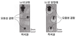
도 1 에 예시한 실시형태에 준하여 본 발명을 실시하였다. 검사 대상의 금속띠로서, 판두께 0.5 ㎜, 판폭 1000 ㎜ 의 강판에 아연 도금을 실시한 아연 도금 강판을 사용하였다. 본 발명예에서는, 동일 지점에 적색광과 청색광을, 적색광은 적색 LED 로 이루어지는 적색 광원으로, 청색광은 청색 LED 로 이루어지는 청색 광원으로 동시에 조사하고, 적색광의 정반사광을 적색 필터를 개재하여 디지털 모노크롬 카메라로 이루어지는 제 1 촬상부에서 수광하여 촬영하고, 청색광의 난반사광을 청색 필터를 개재하여 디지털 모노크롬 카메라로 이루어지는 제 2 촬상부에서 수광하여 촬영하였다. 이때, 제 2 촬상부는, 청색 광원의 광축과 30 도의 각도를 이루는 난반사광의 주광선과 제 2 촬상부의 광축이 일치하도록 배치하였다. 그리고, 제 1 촬상부에 의한 적색광의 정반사광의 촬영 화상을 관찰하여 괴상의 암부 및/또는 괴상의 명부를 요철성 결함과 동정함으로써 요철성 결함의 존재를 검출하고, 또한, 제 2 촬상부에 의한 청색광의 난반사광의 촬영 화상을 관찰하여 명부를 무늬상 결함과 동정함으로써 무늬상 결함의 존재를 검출하였다. 한편, 비교예에서는, 본 발명예에 있어서의 적색 광원 및 청색 광원의 각각 대신에, 백색광을 조사하는 백색 광원으로 하고, 또한, 적색 필터와 청색 필터를 제거하고, 그 이외는 본 발명예와 동일하게 하였다.The present invention was implemented according to the embodiment illustrated in FIG. 1 . As the metal strip to be inspected, a galvanized steel sheet obtained by galvanizing a steel sheet having a sheet thickness of 0.5 mm and a sheet width of 1000 mm was used. In the example of the present invention, red light and blue light are simultaneously irradiated to the same spot, the red light is irradiated with a red light source composed of a red LED, and the blue light is simultaneously irradiated with a blue light source composed of a blue LED, and the regular reflection of the red light is transmitted to a digital monochrome camera through a red filter. The image was taken by receiving light from the first imaging unit formed by the first imaging unit, and received and photographed diffusely reflected blue light by the second imaging unit comprising a digital monochrome camera through a blue filter. At this time, the second imaging unit is arranged so that the optical axis of the second imaging unit coincides with the chief ray of the diffused reflected light forming an angle of 30 degrees with the optical axis of the blue light source. Then, the existence of the concavo-convex defect is detected by observing the photographed image of the regular reflection light of red light by the first imaging unit and identifying the concavo-convex defect and/or the concavo-convex dark portion and/or the concavo-convex defect. The existence of the pattern-like defect was detected by observing the photographed image of the diffused reflection of blue light and identifying the bright part with the pattern-like defect. On the other hand, in the comparative example, instead of each of the red light source and the blue light source in the example of the present invention, a white light source for irradiating white light was used, and the red filter and the blue filter were removed, and other than that were the same as the example of the present invention. made it
도 9 에는, 본 발명예 및 비교예에 있어서의 요철성 결함의 촬영 화상을 나타낸다. 도 9 에 있어서 검은 부분이 요철성 결함을 나타낸다. 도 9(a) 에 나타내는 바와 같이, 요철성 결함은 비교예에서도 검출되기는 하지만, 그 윤곽은 희미해져 있다. 이것에 대해, 도 9(b) 에 나타내는 바와 같이, 본 발명예에서는, 요철성 결함의 윤곽이 보다 명확해져, 검출의 신뢰성이 향상된 것을 알 수 있다. 또, 도 10 에는, 본 발명예 및 비교예에 있어서의 무늬상 결함의 촬영 화상을 나타낸다. 도 10 에 있어서, 흰 부분이 무늬상 결함이다. 도 10(a) 에 나타내는 바와 같이, 비교예에서는, 무늬상 결함은 그 화상이 불선명하여 검출하는 것이 곤란하다. 이에 대하여, 도 10(b) 에 나타내는 바와 같이, 본 발명예에서는, 무늬상 결함은 그 화상이 현격히 선명하여, 무늬상 결함의 존재를 일목 요연하게 검출할 수 있는 것을 알 수 있다. 또, 도 9(b) 및 도 10(b) 로부터, 본 발명예에서는, 요철성 결함 및 무늬상 결함 모두 명확하게 검출할 수 있었던 것을 알 수 있다.9 shows captured images of concavo-convex defects in examples of the present invention and comparative examples. In Fig. 9, black portions represent concavo-convex defects. As shown in Fig. 9(a), concavo-convex defects are also detected in the comparative example, but their contours are blurred. On the other hand, as shown in Fig. 9(b), in the example of the present invention, it is found that the outline of the concavo-convex defect became clearer and the reliability of detection improved. 10 shows captured images of pattern-like defects in examples of the present invention and comparative examples. In Fig. 10, the white portion is a pattern defect. As shown in Fig. 10(a), in the comparative example, pattern-like defects are difficult to detect because the image is blurry. On the other hand, as shown in Fig. 10(b), in the example of the present invention, the image of the pattern-like defect is remarkably clear, and it can be seen that the presence of the pattern-like defect can be detected clearly at a glance. Moreover, from FIG.9(b) and FIG.10(b), in the example of this invention, it turns out that both concavo-convex defect and pattern-like defect were able to be detected clearly.
이상, 본 발명자들에 의해 이루어진 발명을 적용한 실시형태에 대해 설명했지만, 본 실시형태에 의한 본 발명의 개시의 일부를 이루는 기술 및 도면에 의해 본 발명은 한정되지 않는다. 즉, 본 실시형태에 기초하여 당업자 등에 의해 이루어지는 다른 실시형태, 실시예, 및 운용 기술 등은 모두 본 발명의 범주에 포함된다.In the above, the embodiment to which the invention made by the present inventors is applied has been described, but the present invention is not limited by the description and drawings constituting a part of the disclosure of the present invention according to the embodiment. That is, other embodiments, examples, operation techniques, etc. made by those skilled in the art based on the present embodiment are all included in the scope of the present invention.
본 발명에 의하면, 요철상 결함과 무늬상 결함이라는 상이한 종류의 표면 결함에 대한 검출 정밀도를 향상시킴과 함께, 표면 결함의 종류를 판별하는 것이 가능한 금속띠의 표면 검사 장치 및 표면 검사 방법을 제공할 수 있다. 또, 본 발명에 의하면, 금속띠의 제조 수율을 향상 가능한 금속띠의 제조 방법을 제공할 수 있다.According to the present invention, it is possible to provide a surface inspection device and a surface inspection method for a metal strip capable of improving detection accuracy for different types of surface defects, such as concavo-convex defects and pattern-like defects, and discriminating the type of surface defect. can Further, according to the present invention, it is possible to provide a method for manufacturing a metal strip capable of improving the yield of manufacturing a metal strip.
1 : 표면 검사 장치
2 : 제 1 광원부
3 : 제 1 촬상부
3a : 제 1 광학 필터부
4 : 제 2 광원부
5 : 제 2 촬상부
5a : 제 2 광학 필터부
20 : 표면 결함 판별부
L : 법선
L1, L3 : 출사광
L2 : 정반사광
L4 : 난반사광
S : 금속띠1: Surface Inspection Device
2: first light source
3: first imaging unit
3a: first optical filter unit
4: 2nd light source
5: 2nd imaging unit
5a: second optical filter unit
20: surface defect determination unit
L: normal
L1, L3: outgoing light
L2: specular reflection light
L4: Diffuse reflection light
S: metal belt
Claims (10)
상기 제 1 광원부로부터의 출사광에 의한 상기 금속띠의 표면에 있어서의 정반사광을 촬상하는 제 1 촬상부와,
상기 제 1 광원부의 출사광과는 상이한 파장대의 광을 상기 금속띠의 표면에 출사하는 제 2 광원부와,
상기 제 2 광원부로부터의 출사광에 의한 상기 금속띠의 표면에 있어서의 난반사광을 촬상하는 제 2 촬상부와,
상기 제 1 촬상부에 의해 촬상된 정반사광과 상기 제 2 촬상부에 의해 촬상된 난반사광을 사용하여, 상기 금속띠의 표면 결함의 판별을 실시하는 표면 결함 판별부를 구비하고,
상기 제 1 광원부로부터의 출사광 및 상기 제 2 광원부로부터의 출사광은, 상기 금속띠의 표면의 동일 지점에 동시에 조사되는, 금속띠의 표면 검사 장치.a first light source unit for emitting light to the surface of the metal strip;
a first imaging unit that captures an image of light emitted from the first light source unit and regularly reflected on the surface of the metal strip;
a second light source unit for emitting light of a different wavelength range from that of the first light source unit to the surface of the metal strip;
a second imaging unit that captures an image of light emitted from the second light source unit and diffusely reflected light on the surface of the metal strip;
a surface defect discriminating unit configured to determine surface defects of the metal strip using the regular reflected light imaged by the first imaging unit and the diffuse reflected light imaged by the second imaging unit;
The light emitted from the first light source unit and the light emitted from the second light source unit are simultaneously irradiated to the same point on the surface of the metal strip.
상기 제 1 촬상부는, 상기 제 1 광원부로부터의 출사광의 파장 성분을 선택적으로 투과하는 제 1 광학 필터부를 구비하고, 상기 제 2 촬상부는, 상기 제 2 광원부로부터의 출사광의 파장 성분을 선택적으로 투과하는 제 2 광학 필터부를 구비하는, 금속띠의 표면 검사 장치.According to claim 1,
The first imaging unit includes a first optical filter unit that selectively transmits wavelength components of light emitted from the first light source unit, and the second imaging unit selectively transmits wavelength components of light emitted from the second light source unit. A surface inspection device for a metal strip, comprising a second optical filter unit.
상기 제 1 광원부로부터의 출사광은, 상기 제 2 광원부로부터의 출사광보다 장파장의 파장대에서 선택된 광인, 금속띠의 표면 검사 장치.According to claim 1 or 2,
The light emitted from the first light source unit is light selected from a wavelength range having a longer wavelength than the light emitted from the second light source unit.
상기 제 1 광원부로부터의 출사광은, 난색의 파장대에서 선택된 광이며, 상기 제 2 광원부로부터의 출사광은, 한색의 파장대에서 선택된 광인, 금속띠의 표면 검사 장치.According to any one of claims 1 to 3,
The light emitted from the first light source unit is light selected from a warm color wavelength range, and the emitted light from the second light source unit is light selected from a cool color wavelength range.
상기 제 2 광원부로부터의 출사광의 상기 금속띠에의 입사 각도는, 상기 제 1 광원부로부터의 출사광의 상기 금속띠에의 입사각도보다 큰, 금속띠의 표면 검사 장치.According to any one of claims 1 to 4,
wherein an angle of incidence of light emitted from the second light source unit onto the metal strip is larger than an angle of incidence of light emitted from the first light source unit onto the metal strip.
상기 제 1 촬상부의 광축은, 상기 금속띠의 법선에 대해 0°이상 75°이하의 각도이며, 상기 제 2 촬상부의 광축은, 상기 금속띠의 법선에 대해 20°이상 90°미만의 각도인, 금속띠의 표면 검사 장치.According to any one of claims 1 to 5,
The optical axis of the first imaging unit has an angle of 0° or more and 75° or less with respect to the normal of the metal strip, and the optical axis of the second imaging unit has an angle of 20° or more and less than 90° with respect to the normal of the metal strip; A device for inspecting the surface of metal strips.
상기 제 1 광원부 및 상기 제 2 광원부는, 상기 금속띠의 표면에 라인상으로 광을 조사하는 라인상 광원인, 금속띠의 표면 검사 장치.According to any one of claims 1 to 6,
The first light source unit and the second light source unit are line-shaped light sources for irradiating light in a line shape to the surface of the metal strip.
제 1 촬상부를 이용하여 상기 제 1 광원부로부터의 출사광에 의한 상기 금속띠의 표면에 있어서의 정반사광을 촬상하는 제 1 촬상 스텝과,
제 2 광원부를 이용하여 상기 제 1 광원부의 출사광과는 상이한 파장대의 광을 상기 금속띠의 표면에 출사하는 제 2 출사 스텝과,
제 2 촬상부를 이용하여 상기 제 2 광원부로부터의 출사광에 의한 상기 금속띠의 표면에 있어서의 난반사광을 촬상하는 제 2 촬상 스텝과,
상기 제 1 촬상 스텝에 있어서 촬상된 정반사광과 상기 제 2 촬상 스텝에 있어서 촬상된 난반사광을 사용하여, 상기 금속띠의 표면 결함의 판별을 실시하는 스텝을 포함하고,
상기 제 1 광원부로부터의 출사광과 상기 제 2 광원부로부터의 출사광은, 상기 금속띠의 표면의 동일 지점에 동시에 조사되는, 금속띠의 표면 검사 방법.a first emitting step of emitting light to the surface of the metal strip using a first light source unit;
a first imaging step of capturing an image of regular reflection light on the surface of the metal strip by light emitted from the first light source unit using a first imaging unit;
a second emitting step of emitting light of a different wavelength range from that of the first light source unit to the surface of the metal strip by using a second light source unit;
a second imaging step of capturing an image of diffusely reflected light on the surface of the metal strip by light emitted from the second light source unit using a second imaging unit;
a step of discriminating surface defects of the metal strip using the regular reflected light imaged in the first imaging step and the diffused reflected light imaged in the second imaging step;
wherein the emitted light from the first light source unit and the emitted light from the second light source unit are simultaneously irradiated to the same point on the surface of the metal strip.
상기 제 1 촬상부는, 상기 제 1 광원부로부터의 출사광의 파장 성분을 선택적으로 투과하는 제 1 광학 필터부를 구비하고, 상기 제 2 촬상부는, 상기 제 2 광원부로부터의 출사광의 파장 성분을 선택적으로 투과하는 제 2 광학 필터부를 구비하는, 금속띠의 표면 검사 방법.According to claim 8,
The first imaging unit includes a first optical filter unit that selectively transmits wavelength components of light emitted from the first light source unit, and the second imaging unit selectively transmits wavelength components of light emitted from the second light source unit. A method for inspecting the surface of a metal strip, comprising a second optical filter unit.
Applications Claiming Priority (3)
| Application Number | Priority Date | Filing Date | Title |
|---|---|---|---|
| JPJP-P-2020-133820 | 2020-08-06 | ||
| JP2020133820 | 2020-08-06 | ||
| PCT/JP2021/020340 WO2022030083A1 (en) | 2020-08-06 | 2021-05-28 | Metal strip surface inspection device, surface inspection method, and manufacturing method |
Publications (1)
| Publication Number | Publication Date |
|---|---|
| KR20230017312A true KR20230017312A (en) | 2023-02-03 |
Family
ID=80117940
Family Applications (1)
| Application Number | Title | Priority Date | Filing Date |
|---|---|---|---|
| KR1020227046286A KR20230017312A (en) | 2020-08-06 | 2021-05-28 | Metal strip surface inspection device, surface inspection method, and manufacturing method |
Country Status (7)
| Country | Link |
|---|---|
| US (1) | US20230349836A1 (en) |
| EP (1) | EP4194842A4 (en) |
| JP (1) | JPWO2022030083A1 (en) |
| KR (1) | KR20230017312A (en) |
| CN (1) | CN115867791A (en) |
| MX (1) | MX2023001531A (en) |
| WO (1) | WO2022030083A1 (en) |
Families Citing this family (3)
| Publication number | Priority date | Publication date | Assignee | Title |
|---|---|---|---|---|
| WO2023105849A1 (en) * | 2021-12-07 | 2023-06-15 | パナソニックIpマネジメント株式会社 | Inspecting method and inspecting device |
| CN116500042B (en) * | 2023-05-09 | 2024-01-26 | 哈尔滨工业大学重庆研究院 | Defect detection method, device, system and storage medium |
| CN116359230B (en) * | 2023-05-26 | 2023-08-29 | 北京博兴远志科技有限公司 | Permanent magnet surface concave-convex defect detection system and method |
Citations (3)
| Publication number | Priority date | Publication date | Assignee | Title |
|---|---|---|---|---|
| JPH04113260A (en) | 1990-09-03 | 1992-04-14 | Nkk Corp | Method and apparatus for detecting surface defect |
| JPH05188010A (en) | 1992-01-14 | 1993-07-27 | Nippon Steel Corp | Surface inspecting device |
| JP2003121371A (en) | 2001-10-10 | 2003-04-23 | Nippon Steel Corp | Scratch-inspecting apparatus and method |
Family Cites Families (13)
| Publication number | Priority date | Publication date | Assignee | Title |
|---|---|---|---|---|
| JPS60228943A (en) * | 1984-04-27 | 1985-11-14 | Nippon Steel Corp | Inspection of surface state of stainless steel plate |
| US5087822A (en) * | 1990-06-22 | 1992-02-11 | Alcan International Limited | Illumination system with incident beams from near and far dark field for high speed surface inspection of rolled aluminum sheet |
| JP3021266B2 (en) * | 1994-01-31 | 2000-03-15 | 新日本製鐵株式会社 | Optical steel sheet surface inspection equipment |
| IT1273968B (en) * | 1995-02-24 | 1997-07-11 | Finmeccanica Spa | EQUIPMENT FOR THE OPTICAL DETECTION OF SURFACE DEFECTS IN PARTICULAR FOR LAMINATED TAPES |
| JP3523945B2 (en) * | 1995-09-28 | 2004-04-26 | 日新製鋼株式会社 | Surface inspection method |
| JPH09138201A (en) * | 1995-11-15 | 1997-05-27 | Mitsubishi Electric Corp | Surface inspection apparatus |
| JP2001056297A (en) * | 1999-08-17 | 2001-02-27 | Electro Techno Kk | Surface inspection method and device therefor |
| JP4915057B2 (en) * | 2005-05-12 | 2012-04-11 | Jfeスチール株式会社 | Stainless steel sheet surface inspection method and surface inspection apparatus for stainless steel sheet |
| DE102005031957B4 (en) * | 2005-07-08 | 2007-03-22 | Koenig & Bauer Ag | Apparatus for inspecting a substrate with non-uniform reflective surfaces |
| JP6822494B2 (en) * | 2018-02-05 | 2021-01-27 | Jfeスチール株式会社 | Defect inspection equipment and defect inspection method for steel sheets |
| JP6969500B2 (en) * | 2018-05-28 | 2021-11-24 | 日本製鉄株式会社 | Good / bad judgment method and good / bad judgment device for the surface of dull finish material |
| JP2020027197A (en) * | 2018-08-14 | 2020-02-20 | キヤノン株式会社 | Image forming apparatus and optical sensor |
| JP6863350B2 (en) * | 2018-09-07 | 2021-04-21 | Jfeスチール株式会社 | Metal strip surface inspection method and metal strip surface inspection equipment |
-
2021
- 2021-05-28 US US18/014,305 patent/US20230349836A1/en active Pending
- 2021-05-28 EP EP21853964.1A patent/EP4194842A4/en active Pending
- 2021-05-28 JP JP2021552128A patent/JPWO2022030083A1/ja active Pending
- 2021-05-28 KR KR1020227046286A patent/KR20230017312A/en unknown
- 2021-05-28 MX MX2023001531A patent/MX2023001531A/en unknown
- 2021-05-28 CN CN202180046808.1A patent/CN115867791A/en active Pending
- 2021-05-28 WO PCT/JP2021/020340 patent/WO2022030083A1/en active Application Filing
Patent Citations (3)
| Publication number | Priority date | Publication date | Assignee | Title |
|---|---|---|---|---|
| JPH04113260A (en) | 1990-09-03 | 1992-04-14 | Nkk Corp | Method and apparatus for detecting surface defect |
| JPH05188010A (en) | 1992-01-14 | 1993-07-27 | Nippon Steel Corp | Surface inspecting device |
| JP2003121371A (en) | 2001-10-10 | 2003-04-23 | Nippon Steel Corp | Scratch-inspecting apparatus and method |
Also Published As
| Publication number | Publication date |
|---|---|
| WO2022030083A1 (en) | 2022-02-10 |
| EP4194842A1 (en) | 2023-06-14 |
| MX2023001531A (en) | 2023-03-08 |
| US20230349836A1 (en) | 2023-11-02 |
| CN115867791A (en) | 2023-03-28 |
| JPWO2022030083A1 (en) | 2022-02-10 |
| EP4194842A4 (en) | 2024-01-17 |
Similar Documents
| Publication | Publication Date | Title |
|---|---|---|
| KR20230017312A (en) | Metal strip surface inspection device, surface inspection method, and manufacturing method | |
| US6166393A (en) | Method and apparatus for automatic inspection of moving surfaces | |
| US10267747B2 (en) | Surface defect inspecting device and method for steel sheets | |
| KR101992042B1 (en) | Subject object imaging device, subject sensing method, surface inspection device, and surface inspection method | |
| US10041888B2 (en) | Surface defect inspecting device and method for hot-dip coated steel sheets | |
| US7970202B2 (en) | Method and arrangement for detecting surface and structural defects of a long moving product | |
| US20070286471A1 (en) | Auto Distinction System And Auto Distinction Method | |
| JP2000241362A (en) | Surface quality inspecting apparatus and method | |
| JP6950811B2 (en) | Metal plate surface defect detection method and equipment, and galvanized steel sheet manufacturing method | |
| JP2012251983A (en) | Wrap film wrinkle inspection method and device | |
| JPH07218451A (en) | Device for optically inspecting steel plate for surface flaw | |
| JP6926822B2 (en) | Metal strip surface inspection method and inspection equipment | |
| JP2019207114A (en) | Acceptance/rejection determination method and acceptance/rejection determination device for dull-finished material surface | |
| JP6690519B2 (en) | Device and method for inspecting metal band surface defects | |
| JP2023067750A (en) | Generation method and apparatus of surface defect determination model of metal band, success/failure determination method and apparatus of metal band, and manufacturing method of metal band | |
| JP3687441B2 (en) | Surface flaw marking device and method of manufacturing metal band with marking | |
| JP2023059590A (en) | Surface inspection device for metal strip, surface inspection method, and manufacturing method | |
| JP2021067588A (en) | Surface inspection device for object to be inspected and surface inspection method for object to be inspected | |
| KR100345724B1 (en) | Apparatus for detecting surface defect of strip using multi wavelength light source and color ccd camera | |
| JP4821044B2 (en) | Manufacturing method of metal strip with marking | |
| JP4377872B2 (en) | Surface inspection device | |
| JP2023103957A (en) | Method for determining whether metal band meets criteria and method for manufacturing metal band | |
| TW202400996A (en) | Surface inspection method for metal material, surface inspection apparatus for metal material, and metal material |