KR20220103108A - Semiconductor devices and electronic devices - Google Patents
Semiconductor devices and electronic devices Download PDFInfo
- Publication number
- KR20220103108A KR20220103108A KR1020227016290A KR20227016290A KR20220103108A KR 20220103108 A KR20220103108 A KR 20220103108A KR 1020227016290 A KR1020227016290 A KR 1020227016290A KR 20227016290 A KR20227016290 A KR 20227016290A KR 20220103108 A KR20220103108 A KR 20220103108A
- Authority
- KR
- South Korea
- Prior art keywords
- insulator
- transistor
- semiconductor
- conductor
- memory
- Prior art date
Links
- 239000004065 semiconductor Substances 0.000 title claims abstract description 402
- 230000015654 memory Effects 0.000 claims abstract description 301
- 238000009825 accumulation Methods 0.000 claims abstract description 18
- 230000000903 blocking effect Effects 0.000 claims abstract description 12
- 239000012212 insulator Substances 0.000 claims description 312
- 239000004020 conductor Substances 0.000 claims description 174
- 230000006870 function Effects 0.000 claims description 138
- 238000000034 method Methods 0.000 claims description 75
- 239000011701 zinc Substances 0.000 claims description 27
- 229910052738 indium Inorganic materials 0.000 claims description 12
- APFVFJFRJDLVQX-UHFFFAOYSA-N indium atom Chemical compound [In] APFVFJFRJDLVQX-UHFFFAOYSA-N 0.000 claims description 10
- 229910052725 zinc Inorganic materials 0.000 claims description 8
- HCHKCACWOHOZIP-UHFFFAOYSA-N Zinc Chemical compound [Zn] HCHKCACWOHOZIP-UHFFFAOYSA-N 0.000 claims description 6
- LPQOADBMXVRBNX-UHFFFAOYSA-N ac1ldcw0 Chemical compound Cl.C1CN(C)CCN1C1=C(F)C=C2C(=O)C(C(O)=O)=CN3CCSC1=C32 LPQOADBMXVRBNX-UHFFFAOYSA-N 0.000 abstract 1
- 239000010410 layer Substances 0.000 description 109
- 238000003860 storage Methods 0.000 description 104
- 239000010408 film Substances 0.000 description 96
- 239000000758 substrate Substances 0.000 description 92
- 238000012545 processing Methods 0.000 description 61
- 238000010586 diagram Methods 0.000 description 51
- 239000007789 gas Substances 0.000 description 46
- 239000013078 crystal Substances 0.000 description 45
- 239000000463 material Substances 0.000 description 43
- XUIMIQQOPSSXEZ-UHFFFAOYSA-N Silicon Chemical compound [Si] XUIMIQQOPSSXEZ-UHFFFAOYSA-N 0.000 description 38
- 229910052710 silicon Inorganic materials 0.000 description 38
- 239000010703 silicon Substances 0.000 description 38
- IJGRMHOSHXDMSA-UHFFFAOYSA-N Atomic nitrogen Chemical compound N#N IJGRMHOSHXDMSA-UHFFFAOYSA-N 0.000 description 36
- 229910052760 oxygen Inorganic materials 0.000 description 31
- QVGXLLKOCUKJST-UHFFFAOYSA-N atomic oxygen Chemical compound [O] QVGXLLKOCUKJST-UHFFFAOYSA-N 0.000 description 30
- 229910052751 metal Inorganic materials 0.000 description 30
- 239000001301 oxygen Substances 0.000 description 30
- 239000012535 impurity Substances 0.000 description 29
- 239000002184 metal Substances 0.000 description 28
- 230000002829 reductive effect Effects 0.000 description 24
- 229910044991 metal oxide Inorganic materials 0.000 description 22
- 230000015572 biosynthetic process Effects 0.000 description 21
- 150000004706 metal oxides Chemical class 0.000 description 21
- 230000002093 peripheral effect Effects 0.000 description 21
- VYPSYNLAJGMNEJ-UHFFFAOYSA-N Silicium dioxide Chemical compound O=[Si]=O VYPSYNLAJGMNEJ-UHFFFAOYSA-N 0.000 description 20
- 229910052814 silicon oxide Inorganic materials 0.000 description 19
- 125000004429 atom Chemical group 0.000 description 18
- 229910052757 nitrogen Inorganic materials 0.000 description 18
- 238000000231 atomic layer deposition Methods 0.000 description 17
- 239000001257 hydrogen Substances 0.000 description 17
- 229910052739 hydrogen Inorganic materials 0.000 description 17
- 238000004088 simulation Methods 0.000 description 17
- 102100038716 Cap-specific mRNA (nucleoside-2'-O-)-methyltransferase 2 Human genes 0.000 description 15
- 101710203126 Cap-specific mRNA (nucleoside-2'-O-)-methyltransferase 2 Proteins 0.000 description 15
- UFHFLCQGNIYNRP-UHFFFAOYSA-N Hydrogen Chemical compound [H][H] UFHFLCQGNIYNRP-UHFFFAOYSA-N 0.000 description 15
- -1 Metal Oxide Nitride Chemical class 0.000 description 14
- 238000004891 communication Methods 0.000 description 14
- 101100535994 Caenorhabditis elegans tars-1 gene Proteins 0.000 description 13
- 229910052782 aluminium Inorganic materials 0.000 description 13
- XAGFODPZIPBFFR-UHFFFAOYSA-N aluminium Chemical compound [Al] XAGFODPZIPBFFR-UHFFFAOYSA-N 0.000 description 13
- 229910052735 hafnium Inorganic materials 0.000 description 13
- PXHVJJICTQNCMI-UHFFFAOYSA-N Nickel Chemical compound [Ni] PXHVJJICTQNCMI-UHFFFAOYSA-N 0.000 description 12
- 239000000203 mixture Substances 0.000 description 12
- 238000002441 X-ray diffraction Methods 0.000 description 11
- VBJZVLUMGGDVMO-UHFFFAOYSA-N hafnium atom Chemical compound [Hf] VBJZVLUMGGDVMO-UHFFFAOYSA-N 0.000 description 11
- 150000004767 nitrides Chemical class 0.000 description 11
- 230000007547 defect Effects 0.000 description 10
- 230000000694 effects Effects 0.000 description 10
- 238000010894 electron beam technology Methods 0.000 description 10
- 238000004519 manufacturing process Methods 0.000 description 10
- OKTJSMMVPCPJKN-UHFFFAOYSA-N Carbon Chemical compound [C] OKTJSMMVPCPJKN-UHFFFAOYSA-N 0.000 description 9
- 229910052581 Si3N4 Inorganic materials 0.000 description 9
- 239000002994 raw material Substances 0.000 description 9
- HQVNEWCFYHHQES-UHFFFAOYSA-N silicon nitride Chemical compound N12[Si]34N5[Si]62N3[Si]51N64 HQVNEWCFYHHQES-UHFFFAOYSA-N 0.000 description 9
- 230000008859 change Effects 0.000 description 8
- 229910021420 polycrystalline silicon Inorganic materials 0.000 description 8
- 230000008569 process Effects 0.000 description 8
- WFKWXMTUELFFGS-UHFFFAOYSA-N tungsten Chemical compound [W] WFKWXMTUELFFGS-UHFFFAOYSA-N 0.000 description 8
- 229910052721 tungsten Inorganic materials 0.000 description 8
- 239000010937 tungsten Substances 0.000 description 8
- 101100191136 Arabidopsis thaliana PCMP-A2 gene Proteins 0.000 description 7
- 101100422768 Saccharomyces cerevisiae (strain ATCC 204508 / S288c) SUL2 gene Proteins 0.000 description 7
- 101100048260 Saccharomyces cerevisiae (strain ATCC 204508 / S288c) UBX2 gene Proteins 0.000 description 7
- 229910052799 carbon Inorganic materials 0.000 description 7
- 150000001875 compounds Chemical class 0.000 description 7
- 229910052733 gallium Inorganic materials 0.000 description 7
- 229910000449 hafnium oxide Inorganic materials 0.000 description 7
- 238000001228 spectrum Methods 0.000 description 7
- 101100439298 Caenorhabditis elegans cgt-2 gene Proteins 0.000 description 6
- XEEYBQQBJWHFJM-UHFFFAOYSA-N Iron Chemical compound [Fe] XEEYBQQBJWHFJM-UHFFFAOYSA-N 0.000 description 6
- RTAQQCXQSZGOHL-UHFFFAOYSA-N Titanium Chemical compound [Ti] RTAQQCXQSZGOHL-UHFFFAOYSA-N 0.000 description 6
- XLOMVQKBTHCTTD-UHFFFAOYSA-N Zinc monoxide Chemical compound [Zn]=O XLOMVQKBTHCTTD-UHFFFAOYSA-N 0.000 description 6
- 239000000969 carrier Substances 0.000 description 6
- 238000006243 chemical reaction Methods 0.000 description 6
- 238000005229 chemical vapour deposition Methods 0.000 description 6
- WIHZLLGSGQNAGK-UHFFFAOYSA-N hafnium(4+);oxygen(2-) Chemical compound [O-2].[O-2].[Hf+4] WIHZLLGSGQNAGK-UHFFFAOYSA-N 0.000 description 6
- 230000020169 heat generation Effects 0.000 description 6
- 239000011261 inert gas Substances 0.000 description 6
- 229910052746 lanthanum Inorganic materials 0.000 description 6
- FZLIPJUXYLNCLC-UHFFFAOYSA-N lanthanum atom Chemical compound [La] FZLIPJUXYLNCLC-UHFFFAOYSA-N 0.000 description 6
- 229910052759 nickel Inorganic materials 0.000 description 6
- 229910052715 tantalum Inorganic materials 0.000 description 6
- GUVRBAGPIYLISA-UHFFFAOYSA-N tantalum atom Chemical compound [Ta] GUVRBAGPIYLISA-UHFFFAOYSA-N 0.000 description 6
- 238000002230 thermal chemical vapour deposition Methods 0.000 description 6
- 229910052719 titanium Inorganic materials 0.000 description 6
- 239000010936 titanium Substances 0.000 description 6
- XLYOFNOQVPJJNP-UHFFFAOYSA-N water Substances O XLYOFNOQVPJJNP-UHFFFAOYSA-N 0.000 description 6
- 102100038712 Cap-specific mRNA (nucleoside-2'-O-)-methyltransferase 1 Human genes 0.000 description 5
- 101710203121 Cap-specific mRNA (nucleoside-2'-O-)-methyltransferase 1 Proteins 0.000 description 5
- GYHNNYVSQQEPJS-UHFFFAOYSA-N Gallium Chemical compound [Ga] GYHNNYVSQQEPJS-UHFFFAOYSA-N 0.000 description 5
- 238000004364 calculation method Methods 0.000 description 5
- 230000006378 damage Effects 0.000 description 5
- 238000009826 distribution Methods 0.000 description 5
- 229910052732 germanium Inorganic materials 0.000 description 5
- GNPVGFCGXDBREM-UHFFFAOYSA-N germanium atom Chemical compound [Ge] GNPVGFCGXDBREM-UHFFFAOYSA-N 0.000 description 5
- 238000003384 imaging method Methods 0.000 description 5
- 239000002159 nanocrystal Substances 0.000 description 5
- TWNQGVIAIRXVLR-UHFFFAOYSA-N oxo(oxoalumanyloxy)alumane Chemical compound O=[Al]O[Al]=O TWNQGVIAIRXVLR-UHFFFAOYSA-N 0.000 description 5
- 230000003071 parasitic effect Effects 0.000 description 5
- 239000011347 resin Substances 0.000 description 5
- 229920005989 resin Polymers 0.000 description 5
- 229910052707 ruthenium Inorganic materials 0.000 description 5
- 239000002356 single layer Substances 0.000 description 5
- ZOXJGFHDIHLPTG-UHFFFAOYSA-N Boron Chemical compound [B] ZOXJGFHDIHLPTG-UHFFFAOYSA-N 0.000 description 4
- 101001094647 Homo sapiens Serum paraoxonase/arylesterase 1 Proteins 0.000 description 4
- 101000621061 Homo sapiens Serum paraoxonase/arylesterase 2 Proteins 0.000 description 4
- FYYHWMGAXLPEAU-UHFFFAOYSA-N Magnesium Chemical compound [Mg] FYYHWMGAXLPEAU-UHFFFAOYSA-N 0.000 description 4
- ZOKXTWBITQBERF-UHFFFAOYSA-N Molybdenum Chemical compound [Mo] ZOKXTWBITQBERF-UHFFFAOYSA-N 0.000 description 4
- 101150075681 SCL1 gene Proteins 0.000 description 4
- 102100035476 Serum paraoxonase/arylesterase 1 Human genes 0.000 description 4
- 102100022824 Serum paraoxonase/arylesterase 2 Human genes 0.000 description 4
- QCWXUUIWCKQGHC-UHFFFAOYSA-N Zirconium Chemical compound [Zr] QCWXUUIWCKQGHC-UHFFFAOYSA-N 0.000 description 4
- 229910007541 Zn O Inorganic materials 0.000 description 4
- 230000009471 action Effects 0.000 description 4
- 229910052783 alkali metal Inorganic materials 0.000 description 4
- 150000001340 alkali metals Chemical class 0.000 description 4
- 229910052784 alkaline earth metal Inorganic materials 0.000 description 4
- 150000001342 alkaline earth metals Chemical class 0.000 description 4
- 229910052796 boron Inorganic materials 0.000 description 4
- 150000004770 chalcogenides Chemical class 0.000 description 4
- AJNVQOSZGJRYEI-UHFFFAOYSA-N digallium;oxygen(2-) Chemical compound [O-2].[O-2].[O-2].[Ga+3].[Ga+3] AJNVQOSZGJRYEI-UHFFFAOYSA-N 0.000 description 4
- 229910001195 gallium oxide Inorganic materials 0.000 description 4
- 239000011521 glass Substances 0.000 description 4
- 238000001341 grazing-angle X-ray diffraction Methods 0.000 description 4
- 230000010365 information processing Effects 0.000 description 4
- 229910052749 magnesium Inorganic materials 0.000 description 4
- 239000011777 magnesium Substances 0.000 description 4
- 229910052750 molybdenum Inorganic materials 0.000 description 4
- 239000011733 molybdenum Substances 0.000 description 4
- 239000000523 sample Substances 0.000 description 4
- 238000001004 secondary ion mass spectrometry Methods 0.000 description 4
- MZLGASXMSKOWSE-UHFFFAOYSA-N tantalum nitride Chemical compound [Ta]#N MZLGASXMSKOWSE-UHFFFAOYSA-N 0.000 description 4
- 239000010409 thin film Substances 0.000 description 4
- 229910052727 yttrium Inorganic materials 0.000 description 4
- VWQVUPCCIRVNHF-UHFFFAOYSA-N yttrium atom Chemical compound [Y] VWQVUPCCIRVNHF-UHFFFAOYSA-N 0.000 description 4
- 229910052726 zirconium Inorganic materials 0.000 description 4
- JBRZTFJDHDCESZ-UHFFFAOYSA-N AsGa Chemical compound [As]#[Ga] JBRZTFJDHDCESZ-UHFFFAOYSA-N 0.000 description 3
- 229910001218 Gallium arsenide Inorganic materials 0.000 description 3
- 229910052779 Neodymium Inorganic materials 0.000 description 3
- MWUXSHHQAYIFBG-UHFFFAOYSA-N Nitric oxide Chemical compound O=[N] MWUXSHHQAYIFBG-UHFFFAOYSA-N 0.000 description 3
- OAICVXFJPJFONN-UHFFFAOYSA-N Phosphorus Chemical compound [P] OAICVXFJPJFONN-UHFFFAOYSA-N 0.000 description 3
- KJTLSVCANCCWHF-UHFFFAOYSA-N Ruthenium Chemical compound [Ru] KJTLSVCANCCWHF-UHFFFAOYSA-N 0.000 description 3
- 229910004205 SiNX Inorganic materials 0.000 description 3
- 229910000577 Silicon-germanium Inorganic materials 0.000 description 3
- ATJFFYVFTNAWJD-UHFFFAOYSA-N Tin Chemical compound [Sn] ATJFFYVFTNAWJD-UHFFFAOYSA-N 0.000 description 3
- LEVVHYCKPQWKOP-UHFFFAOYSA-N [Si].[Ge] Chemical compound [Si].[Ge] LEVVHYCKPQWKOP-UHFFFAOYSA-N 0.000 description 3
- 229910045601 alloy Inorganic materials 0.000 description 3
- 239000000956 alloy Substances 0.000 description 3
- 239000003990 capacitor Substances 0.000 description 3
- 238000002003 electron diffraction Methods 0.000 description 3
- 238000002149 energy-dispersive X-ray emission spectroscopy Methods 0.000 description 3
- 230000005669 field effect Effects 0.000 description 3
- 230000010354 integration Effects 0.000 description 3
- 229910052742 iron Inorganic materials 0.000 description 3
- 230000014759 maintenance of location Effects 0.000 description 3
- 239000011159 matrix material Substances 0.000 description 3
- 238000005259 measurement Methods 0.000 description 3
- 238000002488 metal-organic chemical vapour deposition Methods 0.000 description 3
- 239000013081 microcrystal Substances 0.000 description 3
- QEFYFXOXNSNQGX-UHFFFAOYSA-N neodymium atom Chemical compound [Nd] QEFYFXOXNSNQGX-UHFFFAOYSA-N 0.000 description 3
- 230000001151 other effect Effects 0.000 description 3
- 230000036961 partial effect Effects 0.000 description 3
- 229910052698 phosphorus Inorganic materials 0.000 description 3
- 239000011574 phosphorus Substances 0.000 description 3
- 229920005591 polysilicon Polymers 0.000 description 3
- 238000005057 refrigeration Methods 0.000 description 3
- HBMJWWWQQXIZIP-UHFFFAOYSA-N silicon carbide Chemical compound [Si+]#[C-] HBMJWWWQQXIZIP-UHFFFAOYSA-N 0.000 description 3
- 229910010271 silicon carbide Inorganic materials 0.000 description 3
- 229910052712 strontium Inorganic materials 0.000 description 3
- CIOAGBVUUVVLOB-UHFFFAOYSA-N strontium atom Chemical compound [Sr] CIOAGBVUUVVLOB-UHFFFAOYSA-N 0.000 description 3
- 229910052714 tellurium Inorganic materials 0.000 description 3
- PORWMNRCUJJQNO-UHFFFAOYSA-N tellurium atom Chemical compound [Te] PORWMNRCUJJQNO-UHFFFAOYSA-N 0.000 description 3
- 229910052718 tin Inorganic materials 0.000 description 3
- 229910052723 transition metal Inorganic materials 0.000 description 3
- 239000011787 zinc oxide Substances 0.000 description 3
- XKRFYHLGVUSROY-UHFFFAOYSA-N Argon Chemical compound [Ar] XKRFYHLGVUSROY-UHFFFAOYSA-N 0.000 description 2
- 101100439299 Caenorhabditis elegans cgt-3 gene Proteins 0.000 description 2
- 229910052684 Cerium Inorganic materials 0.000 description 2
- YCKRFDGAMUMZLT-UHFFFAOYSA-N Fluorine atom Chemical compound [F] YCKRFDGAMUMZLT-UHFFFAOYSA-N 0.000 description 2
- GQPLMRYTRLFLPF-UHFFFAOYSA-N Nitrous Oxide Chemical compound [O-][N+]#N GQPLMRYTRLFLPF-UHFFFAOYSA-N 0.000 description 2
- NRTOMJZYCJJWKI-UHFFFAOYSA-N Titanium nitride Chemical compound [Ti]#N NRTOMJZYCJJWKI-UHFFFAOYSA-N 0.000 description 2
- 238000004458 analytical method Methods 0.000 description 2
- 230000004888 barrier function Effects 0.000 description 2
- 229910052795 boron group element Inorganic materials 0.000 description 2
- 229910052800 carbon group element Inorganic materials 0.000 description 2
- 230000000747 cardiac effect Effects 0.000 description 2
- 230000015556 catabolic process Effects 0.000 description 2
- ZMIGMASIKSOYAM-UHFFFAOYSA-N cerium Chemical compound [Ce][Ce][Ce][Ce][Ce][Ce][Ce][Ce][Ce][Ce][Ce][Ce][Ce][Ce][Ce][Ce][Ce][Ce][Ce][Ce][Ce][Ce][Ce][Ce][Ce][Ce][Ce][Ce][Ce][Ce][Ce][Ce][Ce][Ce][Ce][Ce][Ce][Ce] ZMIGMASIKSOYAM-UHFFFAOYSA-N 0.000 description 2
- 229910052798 chalcogen Inorganic materials 0.000 description 2
- 150000001787 chalcogens Chemical class 0.000 description 2
- 229910017052 cobalt Inorganic materials 0.000 description 2
- 239000010941 cobalt Substances 0.000 description 2
- GUTLYIVDDKVIGB-UHFFFAOYSA-N cobalt atom Chemical compound [Co] GUTLYIVDDKVIGB-UHFFFAOYSA-N 0.000 description 2
- 239000002131 composite material Substances 0.000 description 2
- 238000012937 correction Methods 0.000 description 2
- 230000003247 decreasing effect Effects 0.000 description 2
- 238000001514 detection method Methods 0.000 description 2
- AXAZMDOAUQTMOW-UHFFFAOYSA-N dimethylzinc Chemical compound C[Zn]C AXAZMDOAUQTMOW-UHFFFAOYSA-N 0.000 description 2
- 238000002524 electron diffraction data Methods 0.000 description 2
- 229910052731 fluorine Inorganic materials 0.000 description 2
- 239000011737 fluorine Substances 0.000 description 2
- 235000012041 food component Nutrition 0.000 description 2
- 239000005417 food ingredient Substances 0.000 description 2
- 238000010438 heat treatment Methods 0.000 description 2
- 150000002431 hydrogen Chemical class 0.000 description 2
- 238000007689 inspection Methods 0.000 description 2
- 238000009413 insulation Methods 0.000 description 2
- 238000010030 laminating Methods 0.000 description 2
- MRELNEQAGSRDBK-UHFFFAOYSA-N lanthanum(3+);oxygen(2-) Chemical compound [O-2].[O-2].[O-2].[La+3].[La+3] MRELNEQAGSRDBK-UHFFFAOYSA-N 0.000 description 2
- 239000007788 liquid Substances 0.000 description 2
- 238000010295 mobile communication Methods 0.000 description 2
- 238000012986 modification Methods 0.000 description 2
- 230000004048 modification Effects 0.000 description 2
- PLDDOISOJJCEMH-UHFFFAOYSA-N neodymium(3+);oxygen(2-) Chemical compound [O-2].[O-2].[O-2].[Nd+3].[Nd+3] PLDDOISOJJCEMH-UHFFFAOYSA-N 0.000 description 2
- 239000007800 oxidant agent Substances 0.000 description 2
- 230000003647 oxidation Effects 0.000 description 2
- 238000007254 oxidation reaction Methods 0.000 description 2
- 125000004430 oxygen atom Chemical group O* 0.000 description 2
- RVTZCBVAJQQJTK-UHFFFAOYSA-N oxygen(2-);zirconium(4+) Chemical compound [O-2].[O-2].[Zr+4] RVTZCBVAJQQJTK-UHFFFAOYSA-N 0.000 description 2
- 230000000704 physical effect Effects 0.000 description 2
- 238000000623 plasma-assisted chemical vapour deposition Methods 0.000 description 2
- 239000004033 plastic Substances 0.000 description 2
- BASFCYQUMIYNBI-UHFFFAOYSA-N platinum Chemical compound [Pt] BASFCYQUMIYNBI-UHFFFAOYSA-N 0.000 description 2
- 229910052696 pnictogen Inorganic materials 0.000 description 2
- 239000002243 precursor Substances 0.000 description 2
- 238000004549 pulsed laser deposition Methods 0.000 description 2
- 239000010453 quartz Substances 0.000 description 2
- 238000011084 recovery Methods 0.000 description 2
- 230000003362 replicative effect Effects 0.000 description 2
- 210000005245 right atrium Anatomy 0.000 description 2
- 210000005241 right ventricle Anatomy 0.000 description 2
- 229910001925 ruthenium oxide Inorganic materials 0.000 description 2
- WOCIAKWEIIZHES-UHFFFAOYSA-N ruthenium(iv) oxide Chemical compound O=[Ru]=O WOCIAKWEIIZHES-UHFFFAOYSA-N 0.000 description 2
- 229910021332 silicide Inorganic materials 0.000 description 2
- FVBUAEGBCNSCDD-UHFFFAOYSA-N silicide(4-) Chemical compound [Si-4] FVBUAEGBCNSCDD-UHFFFAOYSA-N 0.000 description 2
- 229910000679 solder Inorganic materials 0.000 description 2
- 238000005476 soldering Methods 0.000 description 2
- 239000002904 solvent Substances 0.000 description 2
- XCZXGTMEAKBVPV-UHFFFAOYSA-N trimethylgallium Chemical compound C[Ga](C)C XCZXGTMEAKBVPV-UHFFFAOYSA-N 0.000 description 2
- 230000008016 vaporization Effects 0.000 description 2
- 230000003936 working memory Effects 0.000 description 2
- 229910001928 zirconium oxide Inorganic materials 0.000 description 2
- SDDGNMXIOGQCCH-UHFFFAOYSA-N 3-fluoro-n,n-dimethylaniline Chemical compound CN(C)C1=CC=CC(F)=C1 SDDGNMXIOGQCCH-UHFFFAOYSA-N 0.000 description 1
- 101100383242 Candida albicans (strain SC5314 / ATCC MYA-2876) HSX11 gene Proteins 0.000 description 1
- 101100290381 Candida albicans CGT1 gene Proteins 0.000 description 1
- ZAMOUSCENKQFHK-UHFFFAOYSA-N Chlorine atom Chemical compound [Cl] ZAMOUSCENKQFHK-UHFFFAOYSA-N 0.000 description 1
- VYZAMTAEIAYCRO-UHFFFAOYSA-N Chromium Chemical compound [Cr] VYZAMTAEIAYCRO-UHFFFAOYSA-N 0.000 description 1
- RYGMFSIKBFXOCR-UHFFFAOYSA-N Copper Chemical compound [Cu] RYGMFSIKBFXOCR-UHFFFAOYSA-N 0.000 description 1
- 239000004593 Epoxy Substances 0.000 description 1
- JMASRVWKEDWRBT-UHFFFAOYSA-N Gallium nitride Chemical compound [Ga]#N JMASRVWKEDWRBT-UHFFFAOYSA-N 0.000 description 1
- 235000015842 Hesperis Nutrition 0.000 description 1
- 235000012633 Iberis amara Nutrition 0.000 description 1
- DGAQECJNVWCQMB-PUAWFVPOSA-M Ilexoside XXIX Chemical compound C[C@@H]1CC[C@@]2(CC[C@@]3(C(=CC[C@H]4[C@]3(CC[C@@H]5[C@@]4(CC[C@@H](C5(C)C)OS(=O)(=O)[O-])C)C)[C@@H]2[C@]1(C)O)C)C(=O)O[C@H]6[C@@H]([C@H]([C@@H]([C@H](O6)CO)O)O)O.[Na+] DGAQECJNVWCQMB-PUAWFVPOSA-M 0.000 description 1
- GPXJNWSHGFTCBW-UHFFFAOYSA-N Indium phosphide Chemical compound [In]#P GPXJNWSHGFTCBW-UHFFFAOYSA-N 0.000 description 1
- WHXSMMKQMYFTQS-UHFFFAOYSA-N Lithium Chemical compound [Li] WHXSMMKQMYFTQS-UHFFFAOYSA-N 0.000 description 1
- 229910016001 MoSe Inorganic materials 0.000 description 1
- 240000007594 Oryza sativa Species 0.000 description 1
- 235000007164 Oryza sativa Nutrition 0.000 description 1
- CBENFWSGALASAD-UHFFFAOYSA-N Ozone Chemical compound [O-][O+]=O CBENFWSGALASAD-UHFFFAOYSA-N 0.000 description 1
- BUGBHKTXTAQXES-UHFFFAOYSA-N Selenium Chemical compound [Se] BUGBHKTXTAQXES-UHFFFAOYSA-N 0.000 description 1
- BQCADISMDOOEFD-UHFFFAOYSA-N Silver Chemical compound [Ag] BQCADISMDOOEFD-UHFFFAOYSA-N 0.000 description 1
- NINIDFKCEFEMDL-UHFFFAOYSA-N Sulfur Chemical compound [S] NINIDFKCEFEMDL-UHFFFAOYSA-N 0.000 description 1
- 239000007983 Tris buffer Substances 0.000 description 1
- 238000005411 Van der Waals force Methods 0.000 description 1
- JXNGBHURWILWBD-UHFFFAOYSA-N [Se].[Hf] Chemical compound [Se].[Hf] JXNGBHURWILWBD-UHFFFAOYSA-N 0.000 description 1
- INQLNSVYIFCUML-QZTLEVGFSA-N [[(2r,3s,4r,5r)-5-(6-aminopurin-9-yl)-3,4-dihydroxyoxolan-2-yl]methoxy-hydroxyphosphoryl] [(2r,3s,4r,5r)-5-(4-carbamoyl-1,3-thiazol-2-yl)-3,4-dihydroxyoxolan-2-yl]methyl hydrogen phosphate Chemical compound NC(=O)C1=CSC([C@H]2[C@@H]([C@H](O)[C@@H](COP(O)(=O)OP(O)(=O)OC[C@@H]3[C@H]([C@@H](O)[C@@H](O3)N3C4=NC=NC(N)=C4N=C3)O)O2)O)=N1 INQLNSVYIFCUML-QZTLEVGFSA-N 0.000 description 1
- 230000005856 abnormality Effects 0.000 description 1
- 230000002411 adverse Effects 0.000 description 1
- 150000001450 anions Chemical class 0.000 description 1
- 229910052786 argon Inorganic materials 0.000 description 1
- 238000013473 artificial intelligence Methods 0.000 description 1
- 239000012298 atmosphere Substances 0.000 description 1
- 239000002585 base Substances 0.000 description 1
- 229910052790 beryllium Inorganic materials 0.000 description 1
- ATBAMAFKBVZNFJ-UHFFFAOYSA-N beryllium atom Chemical compound [Be] ATBAMAFKBVZNFJ-UHFFFAOYSA-N 0.000 description 1
- WVMYSOZCZHQCSG-UHFFFAOYSA-N bis(sulfanylidene)zirconium Chemical compound S=[Zr]=S WVMYSOZCZHQCSG-UHFFFAOYSA-N 0.000 description 1
- 230000036760 body temperature Effects 0.000 description 1
- 230000005587 bubbling Effects 0.000 description 1
- 239000000872 buffer Substances 0.000 description 1
- 239000012159 carrier gas Substances 0.000 description 1
- 150000001768 cations Chemical class 0.000 description 1
- 239000000919 ceramic Substances 0.000 description 1
- 229910052801 chlorine Inorganic materials 0.000 description 1
- 239000000460 chlorine Substances 0.000 description 1
- 229910052804 chromium Inorganic materials 0.000 description 1
- 239000011651 chromium Substances 0.000 description 1
- 230000000295 complement effect Effects 0.000 description 1
- 239000000470 constituent Substances 0.000 description 1
- 238000001816 cooling Methods 0.000 description 1
- 229910052802 copper Inorganic materials 0.000 description 1
- 239000010949 copper Substances 0.000 description 1
- PMHQVHHXPFUNSP-UHFFFAOYSA-M copper(1+);methylsulfanylmethane;bromide Chemical compound Br[Cu].CSC PMHQVHHXPFUNSP-UHFFFAOYSA-M 0.000 description 1
- 238000005520 cutting process Methods 0.000 description 1
- 238000006731 degradation reaction Methods 0.000 description 1
- 238000013461 design Methods 0.000 description 1
- 238000011161 development Methods 0.000 description 1
- HQWPLXHWEZZGKY-UHFFFAOYSA-N diethylzinc Chemical compound CC[Zn]CC HQWPLXHWEZZGKY-UHFFFAOYSA-N 0.000 description 1
- 238000009792 diffusion process Methods 0.000 description 1
- QKIUAMUSENSFQQ-UHFFFAOYSA-N dimethylazanide Chemical compound C[N-]C QKIUAMUSENSFQQ-UHFFFAOYSA-N 0.000 description 1
- ZYLGGWPMIDHSEZ-UHFFFAOYSA-N dimethylazanide;hafnium(4+) Chemical compound [Hf+4].C[N-]C.C[N-]C.C[N-]C.C[N-]C ZYLGGWPMIDHSEZ-UHFFFAOYSA-N 0.000 description 1
- 230000005684 electric field Effects 0.000 description 1
- 230000005611 electricity Effects 0.000 description 1
- 239000008151 electrolyte solution Substances 0.000 description 1
- 238000005516 engineering process Methods 0.000 description 1
- 230000007613 environmental effect Effects 0.000 description 1
- LIWAQLJGPBVORC-UHFFFAOYSA-N ethylmethylamine Chemical compound CCNC LIWAQLJGPBVORC-UHFFFAOYSA-N 0.000 description 1
- 239000002657 fibrous material Substances 0.000 description 1
- 238000007667 floating Methods 0.000 description 1
- 239000000446 fuel Substances 0.000 description 1
- 230000007274 generation of a signal involved in cell-cell signaling Effects 0.000 description 1
- YBMRDBCBODYGJE-UHFFFAOYSA-N germanium oxide Inorganic materials O=[Ge]=O YBMRDBCBODYGJE-UHFFFAOYSA-N 0.000 description 1
- PCHJSUWPFVWCPO-UHFFFAOYSA-N gold Chemical compound [Au] PCHJSUWPFVWCPO-UHFFFAOYSA-N 0.000 description 1
- 229910052737 gold Inorganic materials 0.000 description 1
- 239000010931 gold Substances 0.000 description 1
- 229910021389 graphene Inorganic materials 0.000 description 1
- 229910002804 graphite Inorganic materials 0.000 description 1
- 239000010439 graphite Substances 0.000 description 1
- 238000000227 grinding Methods 0.000 description 1
- NRJVMVHUISHHQB-UHFFFAOYSA-N hafnium(4+);disulfide Chemical compound [S-2].[S-2].[Hf+4] NRJVMVHUISHHQB-UHFFFAOYSA-N 0.000 description 1
- 125000005843 halogen group Chemical group 0.000 description 1
- 238000002173 high-resolution transmission electron microscopy Methods 0.000 description 1
- 125000004435 hydrogen atom Chemical group [H]* 0.000 description 1
- 229910003437 indium oxide Inorganic materials 0.000 description 1
- PJXISJQVUVHSOJ-UHFFFAOYSA-N indium(iii) oxide Chemical compound [O-2].[O-2].[O-2].[In+3].[In+3] PJXISJQVUVHSOJ-UHFFFAOYSA-N 0.000 description 1
- 238000002347 injection Methods 0.000 description 1
- 239000007924 injection Substances 0.000 description 1
- 239000011229 interlayer Substances 0.000 description 1
- 150000002500 ions Chemical class 0.000 description 1
- 229910052741 iridium Inorganic materials 0.000 description 1
- GKOZUEZYRPOHIO-UHFFFAOYSA-N iridium atom Chemical compound [Ir] GKOZUEZYRPOHIO-UHFFFAOYSA-N 0.000 description 1
- 238000002955 isolation Methods 0.000 description 1
- 239000004973 liquid crystal related substance Substances 0.000 description 1
- 229910052744 lithium Inorganic materials 0.000 description 1
- CPLXHLVBOLITMK-UHFFFAOYSA-N magnesium oxide Inorganic materials [Mg]=O CPLXHLVBOLITMK-UHFFFAOYSA-N 0.000 description 1
- 239000000395 magnesium oxide Substances 0.000 description 1
- AXZKOIWUVFPNLO-UHFFFAOYSA-N magnesium;oxygen(2-) Chemical compound [O-2].[Mg+2] AXZKOIWUVFPNLO-UHFFFAOYSA-N 0.000 description 1
- WPBNNNQJVZRUHP-UHFFFAOYSA-L manganese(2+);methyl n-[[2-(methoxycarbonylcarbamothioylamino)phenyl]carbamothioyl]carbamate;n-[2-(sulfidocarbothioylamino)ethyl]carbamodithioate Chemical compound [Mn+2].[S-]C(=S)NCCNC([S-])=S.COC(=O)NC(=S)NC1=CC=CC=C1NC(=S)NC(=O)OC WPBNNNQJVZRUHP-UHFFFAOYSA-L 0.000 description 1
- 238000013507 mapping Methods 0.000 description 1
- 239000012528 membrane Substances 0.000 description 1
- 230000006386 memory function Effects 0.000 description 1
- 238000002156 mixing Methods 0.000 description 1
- 238000001451 molecular beam epitaxy Methods 0.000 description 1
- MHWZQNGIEIYAQJ-UHFFFAOYSA-N molybdenum diselenide Chemical compound [Se]=[Mo]=[Se] MHWZQNGIEIYAQJ-UHFFFAOYSA-N 0.000 description 1
- CWQXQMHSOZUFJS-UHFFFAOYSA-N molybdenum disulfide Chemical compound S=[Mo]=S CWQXQMHSOZUFJS-UHFFFAOYSA-N 0.000 description 1
- 238000012544 monitoring process Methods 0.000 description 1
- 229910021421 monocrystalline silicon Inorganic materials 0.000 description 1
- RUFLMLWJRZAWLJ-UHFFFAOYSA-N nickel silicide Chemical compound [Ni]=[Si]=[Ni] RUFLMLWJRZAWLJ-UHFFFAOYSA-N 0.000 description 1
- 229910021334 nickel silicide Inorganic materials 0.000 description 1
- 229910052758 niobium Inorganic materials 0.000 description 1
- 239000010955 niobium Substances 0.000 description 1
- GUCVJGMIXFAOAE-UHFFFAOYSA-N niobium atom Chemical compound [Nb] GUCVJGMIXFAOAE-UHFFFAOYSA-N 0.000 description 1
- 125000004433 nitrogen atom Chemical group N* 0.000 description 1
- 229960001730 nitrous oxide Drugs 0.000 description 1
- 235000013842 nitrous oxide Nutrition 0.000 description 1
- 230000001590 oxidative effect Effects 0.000 description 1
- SIWVEOZUMHYXCS-UHFFFAOYSA-N oxo(oxoyttriooxy)yttrium Chemical compound O=[Y]O[Y]=O SIWVEOZUMHYXCS-UHFFFAOYSA-N 0.000 description 1
- PVADDRMAFCOOPC-UHFFFAOYSA-N oxogermanium Chemical compound [Ge]=O PVADDRMAFCOOPC-UHFFFAOYSA-N 0.000 description 1
- BPUBBGLMJRNUCC-UHFFFAOYSA-N oxygen(2-);tantalum(5+) Chemical compound [O-2].[O-2].[O-2].[O-2].[O-2].[Ta+5].[Ta+5] BPUBBGLMJRNUCC-UHFFFAOYSA-N 0.000 description 1
- NFHFRUOZVGFOOS-UHFFFAOYSA-N palladium;triphenylphosphane Chemical compound [Pd].C1=CC=CC=C1P(C=1C=CC=CC=1)C1=CC=CC=C1.C1=CC=CC=C1P(C=1C=CC=CC=1)C1=CC=CC=C1.C1=CC=CC=C1P(C=1C=CC=CC=1)C1=CC=CC=C1.C1=CC=CC=C1P(C=1C=CC=CC=1)C1=CC=CC=C1 NFHFRUOZVGFOOS-UHFFFAOYSA-N 0.000 description 1
- 239000002245 particle Substances 0.000 description 1
- 239000011295 pitch Substances 0.000 description 1
- 238000005268 plasma chemical vapour deposition Methods 0.000 description 1
- 229910052697 platinum Inorganic materials 0.000 description 1
- 229910052699 polonium Inorganic materials 0.000 description 1
- HZEBHPIOVYHPMT-UHFFFAOYSA-N polonium atom Chemical compound [Po] HZEBHPIOVYHPMT-UHFFFAOYSA-N 0.000 description 1
- 229920001296 polysiloxane Polymers 0.000 description 1
- 230000006798 recombination Effects 0.000 description 1
- 230000009467 reduction Effects 0.000 description 1
- 230000003252 repetitive effect Effects 0.000 description 1
- 230000029058 respiratory gaseous exchange Effects 0.000 description 1
- 230000004043 responsiveness Effects 0.000 description 1
- 235000009566 rice Nutrition 0.000 description 1
- 229910052594 sapphire Inorganic materials 0.000 description 1
- 239000010980 sapphire Substances 0.000 description 1
- 229910052711 selenium Inorganic materials 0.000 description 1
- 239000011669 selenium Substances 0.000 description 1
- HVEIXSLGUCQTMP-UHFFFAOYSA-N selenium(2-);zirconium(4+) Chemical compound [Se-2].[Se-2].[Zr+4] HVEIXSLGUCQTMP-UHFFFAOYSA-N 0.000 description 1
- 229910021428 silicene Inorganic materials 0.000 description 1
- 229910052709 silver Inorganic materials 0.000 description 1
- 239000004332 silver Substances 0.000 description 1
- 229910052708 sodium Inorganic materials 0.000 description 1
- 239000011734 sodium Substances 0.000 description 1
- 239000007787 solid Substances 0.000 description 1
- 238000004544 sputter deposition Methods 0.000 description 1
- 229910002076 stabilized zirconia Inorganic materials 0.000 description 1
- 230000003068 static effect Effects 0.000 description 1
- 238000012916 structural analysis Methods 0.000 description 1
- 210000001321 subclavian vein Anatomy 0.000 description 1
- 239000000126 substance Substances 0.000 description 1
- 238000006467 substitution reaction Methods 0.000 description 1
- 229910052717 sulfur Inorganic materials 0.000 description 1
- 239000011593 sulfur Substances 0.000 description 1
- 238000001356 surgical procedure Methods 0.000 description 1
- 229910001936 tantalum oxide Inorganic materials 0.000 description 1
- JBQYATWDVHIOAR-UHFFFAOYSA-N tellanylidenegermanium Chemical compound [Te]=[Ge] JBQYATWDVHIOAR-UHFFFAOYSA-N 0.000 description 1
- 150000003624 transition metals Chemical class 0.000 description 1
- 230000005945 translocation Effects 0.000 description 1
- LXEXBJXDGVGRAR-UHFFFAOYSA-N trichloro(trichlorosilyl)silane Chemical compound Cl[Si](Cl)(Cl)[Si](Cl)(Cl)Cl LXEXBJXDGVGRAR-UHFFFAOYSA-N 0.000 description 1
- RGGPNXQUMRMPRA-UHFFFAOYSA-N triethylgallium Chemical compound CC[Ga](CC)CC RGGPNXQUMRMPRA-UHFFFAOYSA-N 0.000 description 1
- MCULRUJILOGHCJ-UHFFFAOYSA-N triisobutylaluminium Chemical compound CC(C)C[Al](CC(C)C)CC(C)C MCULRUJILOGHCJ-UHFFFAOYSA-N 0.000 description 1
- JLTRXTDYQLMHGR-UHFFFAOYSA-N trimethylaluminium Chemical compound C[Al](C)C JLTRXTDYQLMHGR-UHFFFAOYSA-N 0.000 description 1
- IBEFSUTVZWZJEL-UHFFFAOYSA-N trimethylindium Chemical compound C[In](C)C IBEFSUTVZWZJEL-UHFFFAOYSA-N 0.000 description 1
- ITRNXVSDJBHYNJ-UHFFFAOYSA-N tungsten disulfide Chemical compound S=[W]=S ITRNXVSDJBHYNJ-UHFFFAOYSA-N 0.000 description 1
- 229910052720 vanadium Inorganic materials 0.000 description 1
- GPPXJZIENCGNKB-UHFFFAOYSA-N vanadium Chemical compound [V]#[V] GPPXJZIENCGNKB-UHFFFAOYSA-N 0.000 description 1
- 210000003462 vein Anatomy 0.000 description 1
- 208000003663 ventricular fibrillation Diseases 0.000 description 1
- 206010047302 ventricular tachycardia Diseases 0.000 description 1
- 230000000007 visual effect Effects 0.000 description 1
- 238000005406 washing Methods 0.000 description 1
- 239000013585 weight reducing agent Substances 0.000 description 1
- 229910001233 yttria-stabilized zirconia Inorganic materials 0.000 description 1
- YVTHLONGBIQYBO-UHFFFAOYSA-N zinc indium(3+) oxygen(2-) Chemical compound [O--].[Zn++].[In+3] YVTHLONGBIQYBO-UHFFFAOYSA-N 0.000 description 1
- IPSRAFUHLHIWAR-UHFFFAOYSA-N zinc;ethane Chemical compound [Zn+2].[CH2-]C.[CH2-]C IPSRAFUHLHIWAR-UHFFFAOYSA-N 0.000 description 1
Images


Classifications
-
- H—ELECTRICITY
- H10—SEMICONDUCTOR DEVICES; ELECTRIC SOLID-STATE DEVICES NOT OTHERWISE PROVIDED FOR
- H10B—ELECTRONIC MEMORY DEVICES
- H10B43/00—EEPROM devices comprising charge-trapping gate insulators
- H10B43/20—EEPROM devices comprising charge-trapping gate insulators characterised by three-dimensional arrangements, e.g. with cells on different height levels
- H10B43/23—EEPROM devices comprising charge-trapping gate insulators characterised by three-dimensional arrangements, e.g. with cells on different height levels with source and drain on different levels, e.g. with sloping channels
- H10B43/27—EEPROM devices comprising charge-trapping gate insulators characterised by three-dimensional arrangements, e.g. with cells on different height levels with source and drain on different levels, e.g. with sloping channels the channels comprising vertical portions, e.g. U-shaped channels
-
- H01L27/11582—
-
- G—PHYSICS
- G11—INFORMATION STORAGE
- G11C—STATIC STORES
- G11C16/00—Erasable programmable read-only memories
- G11C16/02—Erasable programmable read-only memories electrically programmable
- G11C16/04—Erasable programmable read-only memories electrically programmable using variable threshold transistors, e.g. FAMOS
- G11C16/0483—Erasable programmable read-only memories electrically programmable using variable threshold transistors, e.g. FAMOS comprising cells having several storage transistors connected in series
-
- H01L27/108—
-
- H01L27/1104—
-
- H—ELECTRICITY
- H01—ELECTRIC ELEMENTS
- H01L—SEMICONDUCTOR DEVICES NOT COVERED BY CLASS H10
- H01L29/00—Semiconductor devices specially adapted for rectifying, amplifying, oscillating or switching and having potential barriers; Capacitors or resistors having potential barriers, e.g. a PN-junction depletion layer or carrier concentration layer; Details of semiconductor bodies or of electrodes thereof ; Multistep manufacturing processes therefor
- H01L29/40—Electrodes ; Multistep manufacturing processes therefor
- H01L29/401—Multistep manufacturing processes
- H01L29/4011—Multistep manufacturing processes for data storage electrodes
- H01L29/40117—Multistep manufacturing processes for data storage electrodes the electrodes comprising a charge-trapping insulator
-
- H—ELECTRICITY
- H01—ELECTRIC ELEMENTS
- H01L—SEMICONDUCTOR DEVICES NOT COVERED BY CLASS H10
- H01L29/00—Semiconductor devices specially adapted for rectifying, amplifying, oscillating or switching and having potential barriers; Capacitors or resistors having potential barriers, e.g. a PN-junction depletion layer or carrier concentration layer; Details of semiconductor bodies or of electrodes thereof ; Multistep manufacturing processes therefor
- H01L29/66—Types of semiconductor device ; Multistep manufacturing processes therefor
- H01L29/66007—Multistep manufacturing processes
- H01L29/66075—Multistep manufacturing processes of devices having semiconductor bodies comprising group 14 or group 13/15 materials
- H01L29/66227—Multistep manufacturing processes of devices having semiconductor bodies comprising group 14 or group 13/15 materials the devices being controllable only by the electric current supplied or the electric potential applied, to an electrode which does not carry the current to be rectified, amplified or switched, e.g. three-terminal devices
- H01L29/66409—Unipolar field-effect transistors
- H01L29/66477—Unipolar field-effect transistors with an insulated gate, i.e. MISFET
-
- H—ELECTRICITY
- H01—ELECTRIC ELEMENTS
- H01L—SEMICONDUCTOR DEVICES NOT COVERED BY CLASS H10
- H01L29/00—Semiconductor devices specially adapted for rectifying, amplifying, oscillating or switching and having potential barriers; Capacitors or resistors having potential barriers, e.g. a PN-junction depletion layer or carrier concentration layer; Details of semiconductor bodies or of electrodes thereof ; Multistep manufacturing processes therefor
- H01L29/66—Types of semiconductor device ; Multistep manufacturing processes therefor
- H01L29/68—Types of semiconductor device ; Multistep manufacturing processes therefor controllable by only the electric current supplied, or only the electric potential applied, to an electrode which does not carry the current to be rectified, amplified or switched
- H01L29/76—Unipolar devices, e.g. field effect transistors
- H01L29/772—Field effect transistors
- H01L29/78—Field effect transistors with field effect produced by an insulated gate
- H01L29/786—Thin film transistors, i.e. transistors with a channel being at least partly a thin film
- H01L29/7869—Thin film transistors, i.e. transistors with a channel being at least partly a thin film having a semiconductor body comprising an oxide semiconductor material, e.g. zinc oxide, copper aluminium oxide, cadmium stannate
-
- H—ELECTRICITY
- H10—SEMICONDUCTOR DEVICES; ELECTRIC SOLID-STATE DEVICES NOT OTHERWISE PROVIDED FOR
- H10B—ELECTRONIC MEMORY DEVICES
- H10B10/00—Static random access memory [SRAM] devices
- H10B10/12—Static random access memory [SRAM] devices comprising a MOSFET load element
-
- H—ELECTRICITY
- H10—SEMICONDUCTOR DEVICES; ELECTRIC SOLID-STATE DEVICES NOT OTHERWISE PROVIDED FOR
- H10B—ELECTRONIC MEMORY DEVICES
- H10B12/00—Dynamic random access memory [DRAM] devices
-
- H—ELECTRICITY
- H10—SEMICONDUCTOR DEVICES; ELECTRIC SOLID-STATE DEVICES NOT OTHERWISE PROVIDED FOR
- H10B—ELECTRONIC MEMORY DEVICES
- H10B43/00—EEPROM devices comprising charge-trapping gate insulators
- H10B43/10—EEPROM devices comprising charge-trapping gate insulators characterised by the top-view layout
-
- H—ELECTRICITY
- H01—ELECTRIC ELEMENTS
- H01L—SEMICONDUCTOR DEVICES NOT COVERED BY CLASS H10
- H01L29/00—Semiconductor devices specially adapted for rectifying, amplifying, oscillating or switching and having potential barriers; Capacitors or resistors having potential barriers, e.g. a PN-junction depletion layer or carrier concentration layer; Details of semiconductor bodies or of electrodes thereof ; Multistep manufacturing processes therefor
- H01L29/66—Types of semiconductor device ; Multistep manufacturing processes therefor
- H01L29/68—Types of semiconductor device ; Multistep manufacturing processes therefor controllable by only the electric current supplied, or only the electric potential applied, to an electrode which does not carry the current to be rectified, amplified or switched
- H01L29/76—Unipolar devices, e.g. field effect transistors
- H01L29/772—Field effect transistors
- H01L29/78—Field effect transistors with field effect produced by an insulated gate
- H01L29/786—Thin film transistors, i.e. transistors with a channel being at least partly a thin film
- H01L29/78642—Vertical transistors
-
- H—ELECTRICITY
- H01—ELECTRIC ELEMENTS
- H01L—SEMICONDUCTOR DEVICES NOT COVERED BY CLASS H10
- H01L29/00—Semiconductor devices specially adapted for rectifying, amplifying, oscillating or switching and having potential barriers; Capacitors or resistors having potential barriers, e.g. a PN-junction depletion layer or carrier concentration layer; Details of semiconductor bodies or of electrodes thereof ; Multistep manufacturing processes therefor
- H01L29/66—Types of semiconductor device ; Multistep manufacturing processes therefor
- H01L29/68—Types of semiconductor device ; Multistep manufacturing processes therefor controllable by only the electric current supplied, or only the electric potential applied, to an electrode which does not carry the current to be rectified, amplified or switched
- H01L29/76—Unipolar devices, e.g. field effect transistors
- H01L29/772—Field effect transistors
- H01L29/78—Field effect transistors with field effect produced by an insulated gate
- H01L29/786—Thin film transistors, i.e. transistors with a channel being at least partly a thin film
- H01L29/78681—Thin film transistors, i.e. transistors with a channel being at least partly a thin film having a semiconductor body comprising AIIIBV or AIIBVI or AIVBVI semiconductor materials, or Se or Te
-
- H—ELECTRICITY
- H10—SEMICONDUCTOR DEVICES; ELECTRIC SOLID-STATE DEVICES NOT OTHERWISE PROVIDED FOR
- H10B—ELECTRONIC MEMORY DEVICES
- H10B43/00—EEPROM devices comprising charge-trapping gate insulators
- H10B43/40—EEPROM devices comprising charge-trapping gate insulators characterised by the peripheral circuit region
Landscapes
- Engineering & Computer Science (AREA)
- Microelectronics & Electronic Packaging (AREA)
- Power Engineering (AREA)
- Physics & Mathematics (AREA)
- Ceramic Engineering (AREA)
- Condensed Matter Physics & Semiconductors (AREA)
- General Physics & Mathematics (AREA)
- Computer Hardware Design (AREA)
- Manufacturing & Machinery (AREA)
- Semiconductor Memories (AREA)
- Thin Film Transistor (AREA)
Abstract
신규 반도체 장치를 제공한다. Z 방향으로 연장되는 메모리 스트링이고, 반도체층에 산화물 반도체를 사용함으로써, 고속 동작이 실현된다. 메모리 스트링은 MONOS형 메모리 셀을 포함하고, 제어 게이트 측에 터널층을 제공하고, 반도체 측에 차단층을 제공한다. 소거 동작 시에 제어 게이트 측으로부터 전하 축적층에 정공을 주입한다.A novel semiconductor device is provided. It is a memory string extending in the Z direction, and high-speed operation is realized by using an oxide semiconductor for the semiconductor layer. The memory string includes MONOS type memory cells, provides a tunnel layer on the control gate side, and provides a blocking layer on the semiconductor side. During the erase operation, holes are injected into the charge accumulation layer from the control gate side.
Description
본 발명의 일 형태는 반도체 장치 및 전자 기기에 관한 것이다.One embodiment of the present invention relates to a semiconductor device and an electronic device.
또한 본 발명의 일 형태는 상기 기술분야에 한정되지 않는다. 본 명세서 등에서 개시(開示)하는 발명의 기술분야는 물건, 방법, 또는 제조 방법에 관한 것이다. 또는 본 발명의 일 형태는 공정(process), 기계(machine), 제품(manufacture), 또는 조성물(composition of matter)에 관한 것이다. 그러므로 더 구체적으로 본 명세서에서 개시하는 본 발명의 일 형태의 기술분야로서는 반도체 장치, 표시 장치, 액정 표시 장치, 발광 장치, 축전 장치, 촬상 장치, 기억 장치, 신호 처리 장치, 프로세서, 전자 기기, 시스템, 이들의 구동 방법, 이들의 제조 방법, 또는 이들의 검사 방법을 일례로서 들 수 있다.In addition, one aspect of this invention is not limited to the said technical field. The technical field of the invention disclosed in this specification and the like relates to an article, a method, or a manufacturing method. Or one aspect of the present invention relates to a process, a machine, a product (manufacture), or a composition (composition of matter). Therefore, more specifically, as a technical field of one embodiment of the present invention disclosed in this specification, a semiconductor device, a display device, a liquid crystal display device, a light emitting device, a power storage device, an imaging device, a memory device, a signal processing device, a processor, an electronic device, and a system , their driving method, their manufacturing method, or their inspection method are exemplified.
컴퓨터에 사용하는 대용량 기억 장치로서 NAND형 플래시 메모리가 보급되고 있다. 근년에는 메모리 셀을 3차원적으로 배치함으로써 NAND형 플래시 메모리의 집적도를 높이는 기술이 보급되고 있다(특허문헌 1). 본 명세서 등에서는, 메모리 셀이 3차원적으로 배치된 NAND형 플래시 메모리를 "3D-NAND"라고 부른다.As a mass storage device used in a computer, NAND-type flash memory has become popular. In recent years, a technique for increasing the degree of integration of a NAND-type flash memory by three-dimensionally arranging memory cells has been popularized (Patent Document 1). In this specification and the like, a NAND-type flash memory in which memory cells are arranged three-dimensionally is called "3D-NAND".
3D-NAND의 메모리 스트링은 그 바디부에 다결정 실리콘을 사용하는 경우가 많지만, 특허문헌 2에는 메모리 스트링의 바디부에 산화물 반도체를 사용한 예가 개시되어 있다. 또한 여기서 바디부란, 메모리 스트링을 구성하는 트랜지스터의 채널 또는 소스/드레인으로서 기능하는 반도체층을 가리킨다.Although polycrystalline silicon is often used for the body of the 3D-NAND memory string,
3D-NAND의 소거 동작은 바디부에 정공을 공급함으로써 수행된다. 바디부에 정공을 공급하는 방법으로서, 특허문헌 1에는 (1) GIDL(Gate Induced Drain Leakage)에 의하여 정공을 생성하는 방법과, (2) 반도체 기판의 P-well로부터 정공을 주입하는 방법과, (3) p형 폴리실리콘으로 구성된 콘택트층으로부터 정공을 주입하는 방법이 개시되어 있다.The erase operation of the 3D-NAND is performed by supplying holes to the body. As a method of supplying holes to the body portion,
그러나 바디부에 산화물 반도체를 사용한 경우, 상기 (1) 내지 (3)의 방법은 모두 사용할 수 없다. 예를 들어 (1)의 방법은 산화물 반도체의 밴드 갭이 넓고, GIDL이 발생하지 않는다는 이유로 사용할 수 없다. 또한 (2) 및 (3)의 방법은 p형 폴리실리콘으로부터 산화물 반도체에 정공을 주입하는 경우의 에너지 장벽이 높다는 이유로 사용할 수 없다. 그러므로 3D-NAND는 단순히 바디부를 폴리실리콘으로부터 산화물 반도체로 치환하는 것만으로는 소거 동작을 수행할 수 없다.However, when an oxide semiconductor is used in the body, the methods (1) to (3) above cannot be all used. For example, the method (1) cannot be used because the band gap of the oxide semiconductor is wide and GIDL does not occur. In addition, the methods (2) and (3) cannot be used because the energy barrier in the case of injecting holes from p-type polysilicon into the oxide semiconductor is high. Therefore, the 3D-NAND cannot perform an erase operation by simply replacing the body portion with an oxide semiconductor from polysilicon.
본 발명의 일 형태는 신규 기억 장치를 제공하는 것을 과제 중 하나로 한다. 또는 본 발명의 일 형태는 동작 속도가 빠른 기억 장치를 제공하는 것을 과제 중 하나로 한다. 또는 본 발명의 일 형태는 신뢰성이 높은 기억 장치를 제공하는 것을 과제 중 하나로 한다. 또는 본 발명의 일 형태는 기억 용량이 큰 기억 장치를 제공하는 것을 과제 중 하나로 한다. 또는 본 발명의 일 형태는 신규 반도체 장치를 제공하는 것을 과제 중 하나로 한다. 또는 본 발명의 일 형태는 동작 속도가 빠른 반도체 장치를 제공하는 것을 과제 중 하나로 한다. 또는 본 발명의 일 형태는 신뢰성이 높은 반도체 장치를 제공하는 것을 과제 중 하나로 한다. 또는 본 발명의 일 형태는 기억 용량이 큰 반도체 장치를 제공하는 것을 과제 중 하나로 한다.One aspect of the present invention makes it one of the problems to provide a novel storage device. Another object of one embodiment of the present invention is to provide a memory device having a high operating speed. Another object of one embodiment of the present invention is to provide a highly reliable memory device. Another object of one embodiment of the present invention is to provide a storage device having a large storage capacity. Another object of one embodiment of the present invention is to provide a novel semiconductor device. Another object of one embodiment of the present invention is to provide a semiconductor device having a high operating speed. Another object of one embodiment of the present invention is to provide a highly reliable semiconductor device. Another object of one embodiment of the present invention is to provide a semiconductor device having a large storage capacity.
또한 본 발명의 일 형태의 과제는 위에서 열거한 과제에 한정되지 않는다. 위에서 열거한 과제는 다른 과제의 존재를 방해하는 것이 아니다. 또한 다른 과제는 이하에 기재되고 본 항목에서는 언급되지 않은 과제이다. 본 항목에서 언급되지 않은 과제는 통상의 기술자라면 명세서 또는 도면 등의 기재에서 도출할 수 있는 것이고, 이들 기재에서 적절히 추출할 수 있다. 또한 본 발명의 일 형태는 위에서 열거한 과제 및 다른 과제 중 적어도 하나의 과제를 해결하는 것이다. 또한 본 발명의 일 형태는 위에서 열거한 과제 및 다른 과제 모두를 해결할 필요는 없다.In addition, the subject of one embodiment of this invention is not limited to the subject enumerated above. The tasks listed above do not preclude the existence of other tasks. In addition, other tasks are described below and are not mentioned in this section. Problems not mentioned in this item can be derived from descriptions such as the specification or drawings by those skilled in the art, and can be appropriately extracted from these descriptions. Another aspect of the present invention is to solve at least one of the above-listed problems and other problems. In addition, one embodiment of the present invention does not need to solve all of the problems listed above and other problems.
본 발명의 일 형태는 제 1 방향으로 연장되는 구조체와 제 2 방향으로 연장되는 도전체를 포함하고, 구조체는 산화물 반도체와, 제 1 절연체와, 제 2 절연체와, 제 3 절연체를 포함하고, 산화물 반도체는 제 1 방향으로 연장되고, 제 1 절연체는 산화물 반도체에 인접하고, 제 2 절연체는 제 1 절연체에 인접하고, 제 3 절연체는 제 2 절연체에 인접하고, 구조체가 도전체와 교차되는 교차부에서 산화물 반도체, 제 1 절연체, 제 2 절연체, 및 제 3 절연체가 동심으로 배치되고, 교차부에서 도전체는 제 3 절연체에 인접하고, 제 1 절연체는 제 3 절연체보다 두꺼운 반도체 장치이다.One embodiment of the present invention includes a structure extending in a first direction and a conductor extending in a second direction, wherein the structure includes an oxide semiconductor, a first insulator, a second insulator, and a third insulator, the semiconductor extends in a first direction, the first insulator adjoins the oxide semiconductor, the second insulator adjoins the first insulator, the third insulator adjoins the second insulator, and the structure intersects the conductor In a semiconductor device in which an oxide semiconductor, a first insulator, a second insulator, and a third insulator are arranged concentrically, at the intersection the conductor is adjacent to the third insulator, and the first insulator is thicker than the third insulator.
또한 본 발명의 다른 일 형태는 제 1 방향으로 연장되는 구조체와 제 2 방향으로 연장되는 n층(n은 2 이상의 정수(整數))의 도전체를 포함하고, 구조체는 산화물 반도체와, 제 1 절연체와, 제 2 절연체와, 제 3 절연체를 포함하고, 산화물 반도체는 제 1 방향으로 연장되고, 제 1 절연체는 산화물 반도체에 인접하고, 제 2 절연체는 제 1 절연체에 인접하고, 제 3 절연체는 제 2 절연체에 인접하고, 구조체가 n층의 도전체와 교차되는 n군데의 교차부의 각각에서 산화물 반도체, 제 1 절연체, 제 2 절연체, 및 제 3 절연체가 동심으로 배치되고, n군데의 교차부의 각각에서 도전체는 제 3 절연체에 인접하고, 제 1 절연체는 제 3 절연체보다 두꺼운 반도체 장치이다.Another embodiment of the present invention includes a structure extending in a first direction and an n-layer (n is an integer of 2 or more) conductors extending in a second direction, the structure comprising an oxide semiconductor and a first insulator and a second insulator and a third insulator, wherein the oxide semiconductor extends in a first direction, the first insulator is adjacent to the oxide semiconductor, the second insulator is adjacent to the first insulator, and the third insulator is adjacent to the first insulator. An oxide semiconductor, a first insulator, a second insulator, and a third insulator are disposed concentrically at each of n intersections adjacent to the 2 insulators, where the structure intersects the n-layer conductors, each of the n intersections In the semiconductor device, the conductor is adjacent to the third insulator, and the first insulator is thicker than the third insulator.
또한 본 발명의 다른 일 형태는 구조체와, 제 1 도전체와, 제 2 도전체를 포함하고, 구조체는 제 1 방향으로 연장되는 제 1 부분과, 제 1 방향으로 연장되는 제 2 부분과, 제 2 방향으로 연장되는 제 3 부분을 포함하고, 제 1 도전체 및 제 2 도전체는 제 3 방향으로 연장되고, 구조체는 산화물 반도체와, 제 1 절연체와, 제 2 절연체와, 제 3 절연체를 포함하고, 제 1 부분과 제 1 도전체가 교차되는 제 1 교차부에서 산화물 반도체, 제 1 절연체, 제 2 절연체, 및 제 3 절연체가 동심으로 배치되고, 또한 제 1 도전체가 제 3 절연체에 인접하고, 제 2 부분과 제 2 도전체가 교차되는 제 2 교차부에서 산화물 반도체, 제 1 절연체, 제 2 절연체, 및 제 3 절연체가 동심으로 배치되고, 또한 제 2 도전체가 제 3 절연체에 인접하고, 제 1 교차부 및 제 2 교차부의 각각에서 제 1 절연체는 제 3 절연체보다 두꺼운 반도체 장치이다.Another aspect of the present invention includes a structure, a first conductor, and a second conductor, the structure comprising a first portion extending in a first direction, a second portion extending in the first direction, and a second a third portion extending in two directions, the first conductor and the second conductor extending in a third direction, the structure comprising an oxide semiconductor, a first insulator, a second insulator, and a third insulator and an oxide semiconductor, a first insulator, a second insulator, and a third insulator are arranged concentrically at a first intersection where the first portion and the first conductor intersect, and the first conductor is adjacent to the third insulator, At a second intersection where the second portion and the second conductor intersect, an oxide semiconductor, a first insulator, a second insulator, and a third insulator are disposed concentrically, and the second conductor is adjacent to the third insulator, and the first The first insulator at each of the intersection and the second intersection is a semiconductor device thicker than the third insulator.
제 1 방향은 제 2 방향과 직교하는 방향인 것이 바람직하다. 또한 제 1 방향, 제 2 방향, 및 제 3 방향은 서로 직교하는 방향인 것이 바람직하다. 본 발명의 일 형태에 따른 반도체 장치는 NAND형 기억 장치로서 기능할 수 있다. 또한 본 발명의 일 형태에 따른 반도체 장치는 RAM으로서 기능할 수 있다.The first direction is preferably a direction orthogonal to the second direction. Moreover, it is preferable that a 1st direction, a 2nd direction, and a 3rd direction are mutually orthogonal to each other. The semiconductor device according to one embodiment of the present invention can function as a NAND-type memory device. Further, the semiconductor device according to one embodiment of the present invention can function as a RAM.
예를 들어 제 1 절연체가 차단층으로서 기능하고, 제 2 절연체가 전하 축적층으로서 기능하고, 제 3 절연체가 터널층으로서 기능한다.For example, a first insulator functions as a blocking layer, a second insulator functions as a charge accumulation layer, and a third insulator functions as a tunnel layer.
본 발명의 다른 일 형태는 상기 반도체 장치와, 조작 스위치, 배터리, 및 표시부 중 적어도 하나를 포함하는 전자 기기이다.Another embodiment of the present invention is an electronic device including the semiconductor device, at least one of an operation switch, a battery, and a display unit.
본 발명의 일 형태에 의하여 신규 기억 장치를 제공할 수 있다. 또는 본 발명의 일 형태에 의하여 동작 속도가 빠른 기억 장치를 제공할 수 있다. 또는 본 발명의 일 형태에 의하여 신뢰성이 높은 기억 장치를 제공할 수 있다. 또는 본 발명의 일 형태에 의하여 기억 용량이 큰 기억 장치를 제공할 수 있다. 또는 본 발명의 일 형태에 의하여 신규 반도체 장치를 제공할 수 있다. 또는 본 발명의 일 형태에 의하여 동작 속도가 빠른 반도체 장치를 제공할 수 있다. 또는 신뢰성이 높은 반도체 장치를 제공할 수 있다. 또는 본 발명의 일 형태에 의하여 기억 용량이 큰 반도체 장치를 제공할 수 있다.According to one embodiment of the present invention, a novel storage device can be provided. Alternatively, according to one embodiment of the present invention, a memory device having a high operating speed can be provided. Alternatively, a highly reliable memory device can be provided according to one embodiment of the present invention. Alternatively, according to one embodiment of the present invention, a storage device having a large storage capacity can be provided. Alternatively, a novel semiconductor device can be provided according to one embodiment of the present invention. Alternatively, a semiconductor device having a high operating speed can be provided according to one embodiment of the present invention. Alternatively, a highly reliable semiconductor device can be provided. Alternatively, according to one embodiment of the present invention, a semiconductor device having a large storage capacity can be provided.
또한 본 발명의 일 형태의 효과는 위에서 열거한 효과에 한정되지 않는다. 위에서 열거한 효과는 다른 효과의 존재를 방해하는 것이 아니다. 또한 다른 효과는 이하에 기재되고 본 항목에서는 언급되지 않은 효과이다. 본 항목에서 언급되지 않은 효과는 통상의 기술자라면 명세서 또는 도면 등의 기재에서 도출할 수 있는 것이고, 이들 기재에서 적절히 추출할 수 있다. 또한 본 발명의 일 형태는 위에서 열거한 효과 및 다른 효과 중 적어도 하나의 효과를 갖는 것이다. 따라서 본 발명의 일 형태는 경우에 따라서는 위에서 열거한 효과를 갖지 않는 경우도 있다.In addition, the effect of one embodiment of this invention is not limited to the effect enumerated above. The effects listed above do not prevent the existence of other effects. Also, other effects are effects described below and not mentioned in this section. Effects not mentioned in this item can be derived from descriptions such as the specification or drawings by those skilled in the art, and can be appropriately extracted from these descriptions. Also, one embodiment of the present invention has at least one of the effects listed above and other effects. Therefore, one embodiment of the present invention may not have the above-mentioned effects in some cases.
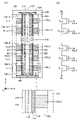
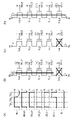
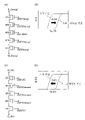
도 1의 (A)는 메모리 스트링의 단면도이다. 도 1의 (B)는 메모리 스트링의 회로도이다.
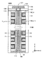
도 2의 (A) 및 (B)는 메모리 스트링의 단면도이다.
도 3의 (A) 및 (B)는 메모리 스트링의 단면도이다.
도 4는 메모리 스트링의 단면도이다.
도 5의 (A) 및 (B)는 메모리 스트링의 단면도이다.
도 6은 메모리 스트링의 단면도이다.
도 7의 (A) 및 (B)는 메모리 스트링의 단면도이다.
도 8의 (A)는 IGZO의 결정 구조의 분류를 설명하는 도면이다. 도 8의 (B)는 CAAC-IGZO막의 XRD 스펙트럼을 설명하는 도면이다. 도 8의 (C)는 CAAC-IGZO막의 나노빔 전자 회절 패턴을 설명하는 도면이다.
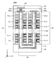
도 9의 (A) 및 (B)는 반도체 장치의 단면도이다.
도 10의 (A) 및 (B)는 반도체 장치의 단면도이다.
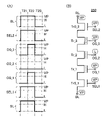
도 11은 반도체 장치의 회로도이다.
도 12의 (A)는 메모리 스트링의 회로도이다. 도 12의 (B)는 트랜지스터의 Id-Vg 특성의 일례를 설명하는 도면이다.
도 13의 (A)는 메모리 스트링의 소거 동작을 설명하는 타이밍 차트이다. 도 13의 (B)는 메모리 스트링의 동작 상태를 나타낸 회로도이다.
도 14의 (A)는 메모리 셀의 단면도이다. 도 14의 (B)는 메모리 셀의 에너지 밴드 다이어그램이다.
도 15의 (A)는 메모리 스트링의 기록 동작을 설명하는 타이밍 차트이다. 도 15의 (B)는 메모리 스트링의 동작 상태를 나타낸 회로도이다.
도 16의 (A)는 메모리 셀의 단면도이다. 도 16의 (B)는 메모리 셀의 에너지 밴드 다이어그램이다.
도 17의 (A)는 메모리 스트링의 판독 동작을 설명하는 타이밍 차트이다. 도 17의 (B) 내지 (D)는 메모리 스트링의 동작 상태를 나타낸 회로도이다.
도 18은 메모리 스트링의 단면도이다.
도 19의 (A), (B)는 메모리 스트링의 단면도이다.
도 20은 메모리 스트링의 회로도이다.
도 21은 메모리 스트링의 단면도이다.
도 22는 메모리 스트링의 단면도이다.
도 23은 메모리 스트링의 단면도이다.
도 24는 메모리 스트링의 단면도이다.
도 25는 메모리 스트링의 단면도이다.
도 26은 메모리 스트링의 단면도이다.
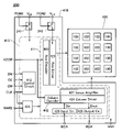
도 27은 반도체 장치의 구성예를 설명하는 블록도이다.
도 28은 반도체 장치의 구성예를 설명하는 도면이다.
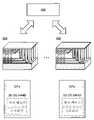
도 29는 복수의 기억 장치를 포함한 정보 처리 시스템의 일례를 설명하는 도면이다.
도 30은 CPU를 설명하는 블록도이다.
도 31의 (A) 및 (B)는 반도체 장치의 사시도이다.
도 32의 (A) 및 (B)는 반도체 장치의 사시도이다.
도 33의 (A) 및 (B)는 반도체 장치의 사시도이다.
도 34의 (A)는 반도체 웨이퍼의 일례를 나타낸 사시도이고, 도 34의 (B)는 칩의 일례를 나타낸 사시도이고, 도 34의 (C) 및 (D)는 전자 부품의 일례를 나타낸 사시도이다.
도 35의 (A) 및 (B)는 각종 기억 장치의 계층을 나타낸 도면이다.
도 36의 (A) 내지 (J)는 전자 기기의 일례를 설명하는 사시도 또는 모식도이다.
도 37의 (A) 내지 (E)는 전자 기기의 일례를 설명하는 사시도 또는 모식도이다.
도 38의 (A) 내지 (C)는 전자 기기의 일례를 설명하는 도면이다.
도 39는 컴퓨터 시스템의 구성예를 설명하는 도면이다.
도 40은 IoT 네트워크의 계층 구조와 요구 사양의 경향을 나타낸 도면이다.
도 41은 공장 자동화의 이미지 도면이다.
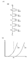
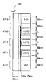
도 42의 (A)는 디바이스 시뮬레이션에서 가정한 메모리 스트링의 등가 회로도이다. 도 42의 (B)는 디바이스 시뮬레이션에서 가정한 메모리 스트링의 단면도이다. 도 42의 (C)는 메모리 트랜지스터의 확대도이다.
도 43의 (A)는 기록 동작에서의 디바이스 시뮬레이션의 설정 전압을 설명하기 위한 도면이다. 도 43의 (B)는 기록 전후에서의 메모리 트랜지스터의 문턱값 변화를 설명하기 위한 도면이다. 도 43의 (C)는 소거 동작에서의 디바이스 시뮬레이션의 설정 전압을 설명하기 위한 도면이다. 도 43의 (D)는 소거 전후에서의 메모리 트랜지스터의 문턱값 변화를 설명하기 위한 도면이다.
도 44의 (A) 및 (B)는 디바이스 시뮬레이션의 계산 결과를 나타낸 그래프이다.
도 45의 (A) 및 (B)는 기록 동작에서의 메모리 스트링 내의 전위 분포를 나타낸 도면이다. 도 45의 (C)는 기록 동작에서의 메모리 트랜지스터 내의 전위 분포를 나타낸 그래프이다.
도 46의 (A) 및 (B)는 소거 동작에서의 디바이스 시뮬레이션의 계산 결과를 나타낸 그래프이다.
도 47은 디바이스 시뮬레이션에서 가정한 값을 나타낸 도면이다.1A is a cross-sectional view of a memory string. 1B is a circuit diagram of a memory string.
2A and 2B are cross-sectional views of a memory string.
3A and 3B are cross-sectional views of a memory string.
4 is a cross-sectional view of a memory string.
5A and 5B are cross-sectional views of a memory string.
6 is a cross-sectional view of a memory string.
7A and 7B are cross-sectional views of a memory string.
Fig. 8(A) is a diagram for explaining the classification of the crystal structure of IGZO. Fig. 8B is a diagram for explaining the XRD spectrum of the CAAC-IGZO film. FIG. 8C is a diagram for explaining a nanobeam electron diffraction pattern of a CAAC-IGZO film.
9A and 9B are cross-sectional views of a semiconductor device.
10A and 10B are cross-sectional views of a semiconductor device.
11 is a circuit diagram of a semiconductor device.
12A is a circuit diagram of a memory string. 12B is a diagram for explaining an example of Id-Vg characteristics of a transistor.
13A is a timing chart for explaining an erase operation of a memory string. 13B is a circuit diagram illustrating an operation state of a memory string.
14A is a cross-sectional view of a memory cell. 14B is an energy band diagram of a memory cell.
Fig. 15A is a timing chart for explaining a write operation of a memory string. 15B is a circuit diagram illustrating an operation state of a memory string.
16A is a cross-sectional view of a memory cell. 16B is an energy band diagram of a memory cell.
Fig. 17A is a timing chart for explaining the read operation of the memory string. 17B to 17D are circuit diagrams illustrating an operation state of a memory string.
18 is a cross-sectional view of a memory string.
19A and 19B are cross-sectional views of a memory string.
20 is a circuit diagram of a memory string.
21 is a cross-sectional view of a memory string.
22 is a cross-sectional view of a memory string.
23 is a cross-sectional view of a memory string.
24 is a cross-sectional view of a memory string.
25 is a cross-sectional view of a memory string.
26 is a cross-sectional view of a memory string.
27 is a block diagram illustrating a configuration example of a semiconductor device.
28 is a diagram for explaining a configuration example of a semiconductor device.
29 is a diagram for explaining an example of an information processing system including a plurality of storage devices.
30 is a block diagram illustrating a CPU.
31A and 31B are perspective views of a semiconductor device.
32A and 32B are perspective views of a semiconductor device.
33A and 33B are perspective views of a semiconductor device.
34A is a perspective view showing an example of a semiconductor wafer, FIG. 34B is a perspective view showing an example of a chip, and FIGS. 34C and 34D are perspective views showing an example of an electronic component .
35A and 35B are diagrams showing the hierarchies of various storage devices.
36A to 36J are perspective views or schematic views for explaining an example of an electronic device.
37A to 37E are perspective views or schematic views for explaining an example of an electronic device.
38A to 38C are diagrams for explaining an example of an electronic device.
Fig. 39 is a diagram for explaining a configuration example of a computer system;
40 is a diagram showing the trend of the hierarchical structure and required specifications of the IoT network.
41 is an image diagram of factory automation.
42A is an equivalent circuit diagram of a memory string assumed in the device simulation. 42B is a cross-sectional view of a memory string assumed in the device simulation. 42C is an enlarged view of the memory transistor.
Fig. 43A is a diagram for explaining the setting voltage of the device simulation in the write operation. 43B is a diagram for explaining a change in the threshold value of the memory transistor before and after writing. 43C is a diagram for explaining a set voltage of device simulation in an erase operation. 43D is a diagram for explaining a change in the threshold value of the memory transistor before and after erasing.
44 (A) and (B) are graphs showing the calculation results of the device simulation.
45A and 45B are diagrams showing potential distribution in a memory string in a write operation. 45C is a graph showing the potential distribution in the memory transistor in the write operation.
46A and 46B are graphs showing calculation results of device simulation in an erase operation.
47 is a diagram showing values assumed in device simulation.
본 명세서 등에서 반도체 장치란, 반도체 특성을 이용한 장치이고, 반도체 소자(트랜지스터, 다이오드, 포토다이오드 등)를 포함한 회로, 이 회로를 포함한 장치 등을 말한다. 또한 반도체 특성을 이용함으로써 기능할 수 있는 장치 전반을 말한다. 예를 들어 집적 회로, 집적 회로를 포함한 칩, 패키지에 칩을 수납한 전자 부품은 반도체 장치의 일례이다. 또한 기억 장치, 표시 장치, 발광 장치, 조명 장치, 및 전자 기기 등은 그 자체가 반도체 장치인 경우나, 반도체 장치를 포함하는 경우가 있다.In this specification and the like, a semiconductor device is a device using semiconductor characteristics, and refers to a circuit including a semiconductor element (transistor, diode, photodiode, etc.), a device including this circuit, and the like. It also refers to the overall device that can function by using semiconductor characteristics. For example, an integrated circuit, a chip including the integrated circuit, and an electronic component housing the chip in a package are examples of semiconductor devices. In addition, a memory device, a display device, a light emitting device, a lighting device, an electronic device, etc. may themselves be a semiconductor device, or may contain a semiconductor device.
또한 본 명세서 등에서 X와 Y가 접속된다고 기재되는 경우에는, X와 Y가 전기적으로 접속되는 경우와, X와 Y가 기능적으로 접속되는 경우와, X와 Y가 직접 접속되는 경우가 본 명세서 등에 개시되어 있는 것으로 한다. 따라서 소정의 접속 관계, 예를 들어 도면 또는 문장에 나타낸 접속 관계에 한정되지 않고, 도면 또는 문장에 나타낸 접속 관계 이외의 것도 도면 또는 문장에 개시되어 있는 것으로 한다. X, Y는 대상물(예를 들어 장치, 소자, 회로, 배선, 전극, 단자, 도전막, 층 등)인 것으로 한다.In addition, when it is described in this specification that X and Y are connected, the case where X and Y are electrically connected, the case where X and Y are functionally connected, and the case where X and Y are directly connected are disclosed in this specification and the like. assumed to be Therefore, it is not limited to the predetermined connection relationship, for example, the connection relationship shown in the drawing or text, and it is assumed that the connection relationship other than the connection relationship shown in the drawing or text is also disclosed in the drawing or text. X and Y shall be objects (for example, devices, elements, circuits, wirings, electrodes, terminals, conductive films, layers, etc.).
X와 Y가 전기적으로 접속되는 경우에는, 일례로서 X와 Y를 전기적으로 접속할 수 있는 소자(예를 들어 스위치, 트랜지스터, 용량 소자, 인덕터, 저항 소자, 다이오드, 표시 디바이스, 발광 디바이스, 부하 등)가 X와 Y 사이에 하나 이상 접속될 수 있다. 또한 스위치는 온 상태와 오프 상태가 제어되는 기능을 갖는다. 즉 스위치는 도통 상태(온 상태) 또는 비도통 상태(오프 상태)가 되어, 전류를 흘릴지 여부를 제어하는 기능을 갖는다.When X and Y are electrically connected, for example, an element capable of electrically connecting X and Y (for example, a switch, a transistor, a capacitor, an inductor, a resistance element, a diode, a display device, a light emitting device, a load, etc.) One or more connections may be made between X and Y. In addition, the switch has a function in which an on state and an off state are controlled. That is, the switch has a function of controlling whether or not a current flows by being in a conduction state (on state) or in a non-conduction state (off state).
X와 Y가 기능적으로 접속되는 경우에는, 일례로서 X와 Y를 기능적으로 접속할 수 있는 회로(예를 들어 논리 회로(인버터, NAND 회로, NOR 회로 등), 신호 변환 회로(디지털 아날로그 변환 회로, 아날로그 디지털 변환 회로, 감마 보정 회로 등), 전위 레벨 변환 회로(전원 회로(승압 회로, 강압 회로 등), 신호의 전위 레벨을 바꾸는 레벨 시프터 회로 등), 전압원, 전류원, 전환 회로, 증폭 회로(신호 진폭 또는 전류량 등을 크게 할 수 있는 회로, 연산 증폭기, 차동 증폭 회로, 소스 폴로어 회로, 버퍼 회로 등), 신호 생성 회로, 기억 회로, 제어 회로 등)가 X와 Y 사이에 하나 이상 접속될 수 있다. 또한 일례로서, X와 Y 사이에 다른 회로를 끼워도 X로부터 출력된 신호가 Y로 전달되는 경우에는, X와 Y는 기능적으로 접속되는 것으로 한다.When X and Y are functionally connected, for example, a circuit capable of functionally connecting X and Y (for example, a logic circuit (inverter, NAND circuit, NOR circuit, etc.), a signal conversion circuit (digital-to-analog conversion circuit, analog Digital conversion circuit, gamma correction circuit, etc.), potential level conversion circuit (power supply circuit (step-up circuit, step-down circuit, etc.), level shifter circuit for changing the potential level of a signal, etc.), voltage source, current source, switching circuit, amplifier circuit (signal amplitude Alternatively, one or more circuits, operational amplifiers, differential amplifier circuits, source follower circuits, buffer circuits, etc.), signal generation circuits, memory circuits, control circuits, etc.) capable of increasing the amount of current, etc. may be connected between X and Y. . Further, as an example, when a signal output from X is transmitted to Y even if another circuit is interposed between X and Y, X and Y are functionally connected.
또한 X와 Y가 전기적으로 접속된다고 명시적으로 기재되는 경우에는, X와 Y가 전기적으로 접속되는 경우(즉 X와 Y가 사이에 다른 소자 또는 다른 회로를 끼워 접속되는 경우)와, X와 Y가 직접 접속되는 경우(즉 X와 Y가 사이에 다른 소자 또는 다른 회로를 끼우지 않고 접속되는 경우)를 포함하는 것으로 한다.In addition, when it is explicitly stated that X and Y are electrically connected, when X and Y are electrically connected (that is, when X and Y are connected by sandwiching another element or another circuit between them), and when X and Y It shall include the case where is directly connected (that is, the case where X and Y are connected without sandwiching another element or another circuit between them).
또한 예를 들어 "X와, Y와, 트랜지스터의 소스(또는 제 1 단자 등)와, 드레인(또는 제 2 단자 등)은 서로 전기적으로 접속되고, X, 트랜지스터의 소스(또는 제 1 단자 등), 트랜지스터의 드레인(또는 제 2 단자 등), Y의 순서로 전기적으로 접속된다"라고 표현할 수 있다. 또는 "트랜지스터의 소스(또는 제 1 단자 등)는 X에 전기적으로 접속되고, 트랜지스터의 드레인(또는 제 2 단자 등)은 Y에 전기적으로 접속되고, X, 트랜지스터의 소스(또는 제 1 단자 등), 트랜지스터의 드레인(또는 제 2 단자 등), Y는 이 순서대로 전기적으로 접속된다"라고 표현할 수 있다. 또는 "X는 트랜지스터의 소스(또는 제 1 단자 등)와 드레인(또는 제 2 단자 등)을 통하여 Y에 전기적으로 접속되고, X, 트랜지스터의 소스(또는 제 1 단자 등), 트랜지스터의 드레인(또는 제 2 단자 등), Y는 이 접속 순서로 제공된다"라고 표현할 수 있다. 이들 예와 같은 표현 방법을 사용하여 회로 구성에서의 접속 순서에 대하여 규정함으로써, 트랜지스터의 소스(또는 제 1 단자 등)와 드레인(또는 제 2 단자 등)을 구별하여 기술적 범위를 결정할 수 있다. 또한 이들 표현 방법은 일례이고, 이들 표현 방법에 한정되지 않는다. 여기서 X, Y는 대상물(예를 들어 장치, 소자, 회로, 배선, 전극, 단자, 도전막, 층 등)인 것으로 한다.Also, for example, "X and Y, the source (or the first terminal, etc.) of the transistor, and the drain (or the second terminal, etc.) are electrically connected to each other, and X, the source (or the first terminal, etc.) of the transistor. , the drain (or the second terminal, etc.) of the transistor, and then electrically connected in the order of Y". or "the source (or first terminal, etc.) of the transistor is electrically connected to X, the drain (or second terminal, etc.) of the transistor is electrically connected to Y, and X, the source (or first terminal, etc.) of the transistor , the drain (or the second terminal, etc.) of the transistor, and Y are electrically connected in this order". or "X is electrically connected to Y through the source (or first terminal, etc.) and drain (or second terminal, etc.) of the transistor, and X, the source (or first terminal, etc.) of the transistor, the drain of the transistor (or second terminal, etc.), Y is provided in this connection order". By specifying the connection order in the circuit configuration using the expression method as in these examples, the source (or the first terminal, etc.) and the drain (or the second terminal, etc.) of the transistor can be distinguished and the technical scope can be determined. In addition, these expression methods are an example, and are not limited to these expression methods. Here, X and Y are assumed to be objects (for example, devices, elements, circuits, wirings, electrodes, terminals, conductive films, layers, etc.).
또한 회로도상 독립된 구성 요소들이 전기적으로 접속되는 것처럼 도시되어 있는 경우에도, 하나의 구성 요소가 복수의 구성 요소의 기능을 겸비하는 경우도 있다. 예를 들어 배선의 일부가 전극으로서도 기능하는 경우에는, 하나의 도전막이 배선의 기능 및 전극의 기능의 양쪽을 겸비한다. 따라서 본 명세서에서의 전기적인 접속이란, 이와 같이 하나의 도전막이 복수의 구성 요소의 기능을 겸비하는 경우도 그 범주에 포함한다.In addition, even when the independent components are illustrated as being electrically connected on the circuit diagram, there is a case where one component has the functions of a plurality of components. For example, when a part of wiring also functions as an electrode, one conductive film has both the function of a wiring and the function of an electrode. Therefore, the electrical connection in this specification includes the case where one conductive film has both the functions of a plurality of components as described above in its category.
또한 본 명세서 등에서 "저항 소자"란, 예를 들어 0Ω보다 저항값이 높은 회로 소자, 배선 등으로 할 수 있다. 그러므로 본 명세서 등에서 "저항 소자"는 저항값을 갖는 배선, 소스와 드레인 간을 전류가 흐르는 트랜지스터, 다이오드, 코일 등을 포함하는 것으로 한다. 그러므로 "저항 소자"라는 용어는 "저항", "부하", "저항값을 갖는 영역" 등의 용어로 바꿔 말할 수 있고, 반대로 "저항", "부하", "저항값을 갖는 영역"이라는 용어는 "저항 소자" 등의 용어로 바꿔 말할 수 있다. 저항값은 예를 들어 바람직하게는 1mΩ 이상 10Ω 이하, 더 바람직하게는 5mΩ 이상 5Ω 이하, 더욱 바람직하게는 10mΩ 이상 1Ω 이하로 할 수 있다. 또한 예를 들어 1Ω 이상 1×10⁹Ω 이하로 하여도 좋다.In this specification and the like, the term "resistive element" can be, for example, a circuit element, wiring, or the like having a resistance value higher than 0 Ω. Therefore, in the present specification and the like, "resistive element" includes a wiring having a resistance value, a transistor through which current flows between a source and a drain, a diode, a coil, and the like. Therefore, the term "resistive element" can be used interchangeably with terms such as "resistance", "load", "region having a resistance value", etc. can be used interchangeably with terms such as "resistive element". The resistance value may be, for example, preferably 1 mΩ or more and 10 Ω or less, more preferably 5 mΩ or more and 5 Ω or less, still more preferably 10 mΩ or more and 1 Ω or less. Moreover, you may set it as 1 ohm or more and 1x10 9 ohm or less, for example.
또한 본 명세서 등에서 "용량 소자"란, 예를 들어 0F보다 정전 용량의 값이 높은 회로 소자, 정전 용량의 값을 갖는 배선의 영역, 기생 용량, 트랜지스터의 게이트 용량 등으로 할 수 있다. 그러므로 본 명세서 등에서 "용량 소자"는 한 쌍의 전극과, 상기 전극 사이에 포함되는 유전체를 포함하는 회로 소자뿐만 아니라, 배선과 배선 사이에 발생하는 기생 용량, 트랜지스터의 소스 및 드레인 중 한쪽과 게이트 사이에 발생하는 게이트 용량 등을 포함하는 것으로 한다. 또한 "용량 소자", "기생 용량", "게이트 용량" 등이라는 용어는 "용량" 등의 용어로 바꿔 말할 수 있고, 반대로 "용량"이라는 용어는 "용량 소자", "기생 용량", "게이트 용량" 등의 용어로 바꿔 말할 수 있다. 또한 "용량"의 "한 쌍의 전극"이라는 용어는 "한 쌍의 도전체", "한 쌍의 도전 영역", "한 쌍의 영역" 등으로 바꿔 말할 수 있다. 또한 정전 용량의 값은 예를 들어 0.05fF 이상 10pF 이하로 할 수 있다. 또한 예를 들어 1pF 이상 10μF 이하로 하여도 좋다.In this specification and the like, "capacitance element" can be, for example, a circuit element having a capacitance value higher than 0F, a region of a wiring having a capacitance value, parasitic capacitance, a gate capacitance of a transistor, and the like. Therefore, in this specification and the like, "capacitance element" refers to not only a circuit element including a pair of electrodes and a dielectric included between the electrodes, but also parasitic capacitance generated between wirings, and between one of the source and drain of the transistor and the gate. It shall include the gate capacitance etc. generated in . Also, the terms "capacitance element", "parasitic capacitance", "gate capacitance", etc. can be used interchangeably with terms such as "capacitance", and conversely, the terms "capacitance" are used interchangeably with "capacitance element", "parasitic capacitance", "gate capacitance". capacity" and the like. In addition, the term "a pair of electrodes" of "capacitance" can be used interchangeably with "a pair of conductors", "a pair of conductive regions", "a pair of regions", and the like. Moreover, the value of electrostatic capacitance can be made into 0.05 fF or more and 10 pF or less, for example. Moreover, you may set it as 1 pF or more and 10 microF or less, for example.
또한 본 명세서 등에서 트랜지스터는 게이트, 소스, 및 드레인이라고 불리는 3개의 단자를 포함한다. 게이트는 트랜지스터의 도통 상태를 제어하는 제어 단자이다. 소스 또는 드레인으로서 기능하는 2개의 단자는 트랜지스터의 입출력 단자이다. 2개의 입출력 단자는 트랜지스터의 도전형(n채널형, p채널형) 및 트랜지스터의 3개의 단자에 인가되는 전위의 높낮이에 따라, 한쪽이 소스가 되고 다른 쪽이 드레인이 된다. 그러므로 본 명세서 등에서는, 소스나 드레인이라는 용어는 바꿔 말할 수 있는 것으로 한다. 또한 본 명세서 등에서는, 트랜지스터의 접속 관계를 설명하는 경우, "소스 및 드레인 중 한쪽"(또는 제 1 전극 또는 제 1 단자), "소스 및 드레인 중 다른 쪽"(또는 제 2 전극 또는 제 2 단자)이라는 표기를 사용한다. 또한 트랜지스터의 구조에 따라서는 상술한 3개의 단자에 더하여 백 게이트를 포함하는 경우가 있다. 이 경우, 본 명세서 등에서 트랜지스터의 게이트 및 백 게이트 중 한쪽을 제 1 게이트라고 부르고, 트랜지스터의 게이트 및 백 게이트 중 다른 쪽을 제 2 게이트라고 부르는 경우가 있다. 또한 같은 트랜지스터에서 "게이트"와 "백 게이트"라는 용어는 서로 바꿀 수 있는 경우가 있다. 또한 트랜지스터가 3개 이상의 게이트를 포함하는 경우, 본 명세서 등에서는 각각의 게이트를 제 1 게이트, 제 2 게이트, 제 3 게이트 등이라고 부를 수 있다.Also, in this specification and the like, a transistor includes three terminals called a gate, a source, and a drain. The gate is a control terminal that controls the conduction state of the transistor. The two terminals serving as source or drain are the input/output terminals of the transistor. One of the input/output terminals becomes a source and the other becomes a drain depending on the conductivity type (n-channel type, p-channel type) of the transistor and the level of potential applied to the three terminals of the transistor. Therefore, in this specification and the like, the terms source and drain are used interchangeably. In this specification and the like, when describing the connection relationship between transistors, "one of the source and the drain" (or the first electrode or the first terminal), "the other of the source and the drain" (or the second electrode or the second terminal) ) is used. Also, depending on the structure of the transistor, a back gate may be included in addition to the above three terminals. In this case, in this specification, one of the gate and the back gate of the transistor may be referred to as a first gate, and the other of the gate and the back gate of the transistor may be referred to as a second gate. Also, in the same transistor, the terms "gate" and "back gate" are sometimes interchangeable. In addition, when the transistor includes three or more gates, each gate may be referred to as a first gate, a second gate, a third gate, etc. in the present specification.
또한 본 명세서 등에서 "노드"는 회로 구성이나 디바이스 구조 등에 따라 단자, 배선, 전극, 도전층, 도전체, 불순물 영역 등으로 바꿔 말할 수 있다. 또한 단자, 배선 등을 "노드"로 바꿔 말할 수 있다.In addition, in this specification and the like, "node" can be interchangeably referred to as a terminal, wiring, electrode, conductive layer, conductor, impurity region, etc. depending on the circuit configuration or device structure. Also, terminals, wires, etc. can be referred to as "nodes".
또한 본 명세서 등에서 "전압"과 "전위"는 적절히 바꿔 말할 수 있다. "전압"은 기준이 되는 전위와의 전위차를 말하고, 예를 들어 기준이 되는 전위를 그라운드 전위(접지 전위)로 하면, "전압"을 "전위"로 바꿔 말할 수 있다. 또한 그라운드 전위는 반드시 0V를 의미하는 것은 아니다. 또한 전위는 상대적인 것이고, 기준이 되는 전위가 변화함으로써, 배선에 공급되는 전위, 회로 등에 인가되는 전위, 회로 등으로부터 출력되는 전위 등도 변화한다.In addition, in this specification and the like, "voltage" and "potential" can be appropriately used interchangeably. "Voltage" refers to a potential difference with a reference potential, and when, for example, the reference potential is the ground potential (ground potential), "voltage" can be changed to "potential". Also, the ground potential does not necessarily mean 0V. Further, the potential is relative, and as the reference potential changes, the potential supplied to the wiring, the potential applied to the circuit or the like, the potential output from the circuit or the like also changes.
또한 본 명세서 등에서 "고레벨 전위("하이 레벨 전위", "H 전위", 또는 "H"라고도 함)", "저레벨 전위("로 레벨 전위", "L 전위", 또는 "L"이라고도 함)"라는 용어는 특정의 전위를 의미하는 것은 아니다. 예를 들어 2개의 배선의 양쪽이 "고레벨 전위를 공급하는 배선으로서 기능한다"라고 기재되는 경우, 양쪽의 배선이 공급하는 각 고레벨 전위는 서로 같지 않아도 된다. 또한 마찬가지로 2개의 배선의 양쪽이 "저레벨 전위를 공급하는 배선으로서 기능한다"라고 기재되는 경우, 양쪽의 배선이 공급하는 각 저레벨 전위는 서로 같지 않아도 된다.In addition, in this specification, etc., "high-level potential (also called "high-level potential", "H potential", or "H")", "low-level potential" (also called "low-level potential", "L potential", or "L") The term " does not imply a specific translocation. For example, when it is described that both of the two wirings "function as a wiring supplying a high-level potential", the respective high-level potentials supplied by both wirings do not have to be equal to each other. Similarly, when it is described that both of the two wirings "functions as wirings supplying low-level potentials", the respective low-level potentials supplied by both wirings do not have to be equal to each other.
"전류"란 전하의 이동 현상(전기 전도)을 말하고, 예를 들어 "양의 하전체(荷電體)의 전기 전도가 발생하고 있다"라는 기재는, "그 반대 방향으로 음의 하전체의 전기 전도가 발생하고 있다"라고 바꿔 말할 수 있다. 그러므로 본 명세서 등에서 "전류"란 별도의 설명이 없는 한, 캐리어의 이동에 따른 전하의 이동 현상(전기 전도)을 말하는 것으로 한다. 여기서 캐리어란 전자, 정공, 음이온, 양이온, 착이온 등이고, 전류가 흐르는 시스템(예를 들어 반도체, 금속, 전해액, 진공 중 등)에 따라 캐리어가 다르다. 또한 배선 등에서의 "전류의 방향"은 양의 캐리어가 이동하는 방향이고, 양의 전류량으로 기재한다. 바꿔 말하면, 음의 캐리어가 이동하는 방향은 전류의 방향과 반대 방향이고, 음의 전류량으로 표현된다. 따라서 본 명세서 등에서 전류의 양과 음(또는 전류의 방향)에 대하여 별도의 설명이 없는 경우, "소자 A로부터 소자 B로 전류가 흐른다" 등의 기재는 "소자 B로부터 소자 A로 전류가 흐른다" 등으로 바꿔 말할 수 있는 것으로 한다. 또한 "소자 A에 전류가 입력된다" 등의 기재는 "소자 A로부터 전류가 출력된다" 등으로 바꿔 말할 수 있는 것으로 한다."Current" refers to a phenomenon of movement of electric charge (electric conduction), for example, the description "electric conduction of a positively charged object is occurring" means "electricity of a negatively charged object in the opposite direction" Conduction is taking place.” Therefore, in the present specification and the like, "current" shall refer to the movement of charges (electric conduction) according to the movement of carriers, unless otherwise specified. Here, a carrier is an electron, a hole, an anion, a cation, a complex ion, etc., and a carrier differs according to the system through which an electric current flows (for example, a semiconductor, a metal, electrolyte solution, in a vacuum, etc.). In addition, the "direction of current" in wiring or the like is the direction in which positive carriers move, and is described as the amount of positive current. In other words, the direction in which the negative carrier moves is opposite to the direction of the current, and is expressed as the amount of negative current. Therefore, in this specification, etc., if there is no separate explanation for the positive and negative currents (or the direction of the current), a description such as “current flows from device A to device B” means “current flows from device B to device A”, etc. make it something that can be changed to In addition, it is assumed that description such as "current is inputted to element A" can be rephrased as "current is outputted from element A" or the like.
또한 본 명세서 등에서 "제 1", "제 2", "제 3"이라는 서수사는 구성 요소의 혼동을 피하기 위하여 붙인 것이다. 따라서 구성 요소의 개수를 한정하는 것이 아니다. 또한 구성 요소의 순서를 한정하는 것이 아니다. 예를 들어 본 명세서 등의 실시형태 중 하나에서 "제 1"로 언급된 구성 요소가 다른 실시형태 또는 청구범위 등에서 "제 2"로 언급된 구성 요소가 될 수도 있다. 또한 예를 들어 본 명세서 등의 실시형태 중 하나에서 "제 1"로 언급된 구성 요소가 다른 실시형태 또는 청구범위 등에서 생략될 수도 있다.In addition, in this specification and the like, ordinal numbers such as "first", "second", and "third" are added to avoid confusion of components. Therefore, the number of components is not limited. Also, the order of the components is not limited. For example, a component referred to as “first” in one of the embodiments in the present specification and the like may be a component referred to as “second” in other embodiments or claims. Also, for example, a component referred to as “first” in one of the embodiments in the present specification and the like may be omitted in other embodiments or claims.
또한 본 명세서 등에서 "위에", "아래에" 등의 배치를 나타내는 용어는 구성끼리의 위치 관계를 도면을 참조하여 설명하기 위하여 편의상 사용하고 있는 경우가 있다. 또한 구성끼리의 위치 관계는 각 구성을 묘사하는 방향에 따라 적절히 변화된다. 따라서 명세서 등에서 설명한 용어에 한정되지 않고, 상황에 따라 적절히 바꿔 말할 수 있다. 예를 들어 "도전체의 상면에 위치하는 절연체"라는 표현은, 나타낸 도면의 방향을 180° 회전시킴으로써, "도전체의 하면에 위치하는 절연체"라고 바꿔 말할 수 있다.In addition, in this specification and the like, terms indicating arrangement such as “above” and “below” are sometimes used for convenience in order to describe the positional relationship between components with reference to the drawings. In addition, the positional relationship between components changes suitably according to the direction in which each structure is described. Therefore, it is not limited to the terminology demonstrated in the specification etc., It can be changed suitably according to a situation. For example, the expression "an insulator located on the upper surface of the conductor" can be changed to "an insulator located on the lower surface of the conductor" by rotating the direction of the illustrated drawing by 180°.
또한 "위"나 "아래"라는 용어는, 구성 요소의 위치 관계가 바로 위 또는 바로 아래이며 직접 접촉하는 것에 한정되지 않는다. 예를 들어 "절연층(A) 위의 전극(B)"이라는 표현이면, 절연층(A) 위에 전극(B)이 직접 접촉되어 형성될 필요는 없고, 절연층(A)과 전극(B) 사이에 다른 구성 요소를 포함하는 것을 제외하지 않는다.In addition, the terms "above" or "below", the positional relationship of the components is directly above or directly below, and is not limited to direct contact. For example, if the expression "electrode (B) on the insulating layer (A)" is used, it is not necessary to directly contact the electrode B on the insulating layer (A), and the insulating layer (A) and the electrode (B) It does not exclude the inclusion of other components in between.
또한 본 명세서 등에서 "막", "층" 등의 용어는 상황에 따라 서로 바꿀 수 있다. 예를 들어 "도전층"이라는 용어를 "도전막"이라는 용어로 변경할 수 있는 경우가 있다. 또는 예를 들어 "절연막"이라는 용어를 "절연층"이라는 용어로 변경할 수 있는 경우가 있다. 또는 경우 또는 상황에 따라 "막", "층" 등의 용어를 사용하지 않고, 다른 용어로 바꿀 수 있다. 예를 들어 "도전층" 또는 "도전막"이라는 용어를 "도전체"라는 용어로 변경할 수 있는 경우가 있다. 또는 예를 들어 "절연층", "절연막"이라는 용어를 "절연체"라는 용어로 변경할 수 있는 경우가 있다.Also, in this specification, terms such as “film” and “layer” may be interchanged with each other depending on circumstances. For example, the term "conductive layer" may be changed to the term "conductive film" in some cases. Alternatively, for example, the term "insulating film" may be changed to the term "insulating layer". Alternatively, terms such as “film” and “layer” may not be used and may be replaced with other terms depending on the case or situation. For example, the term "conductive layer" or "conductive film" may be changed to the term "conductor" in some cases. Alternatively, for example, the terms "insulating layer" and "insulating film" may be changed to the term "insulator".
또한 본 명세서 등에서 "전극", "배선", "단자" 등의 용어는, 이들 구성 요소를 기능적으로 한정하는 것이 아니다. 예를 들어 "전극"은 "배선"의 일부로서 사용되는 경우가 있고, 그 반대도 마찬가지이다. 또한 "전극"이나 "배선"이라는 용어는, 복수의 "전극"이나 "배선"이 일체가 되어 형성되어 있는 경우 등도 포함한다. 또한 예를 들어 "단자"는 "배선"이나 "전극"의 일부로서 사용되는 경우가 있고, 그 반대도 마찬가지이다. 또한 "단자"라는 용어는, 복수의 "전극", "배선", "단자" 등이 일체가 되어 형성되어 있는 경우 등도 포함한다. 그러므로 예를 들어 "전극"은 "배선" 또는 "단자"의 일부가 될 수 있고, 예를 들어 "단자"는 "배선" 또는 "전극"의 일부가 될 수 있다. 또한 "전극", "배선", "단자" 등의 용어는 경우에 따라 "영역" 등의 용어로 치환되는 경우가 있다.In addition, in this specification and the like, terms such as "electrode", "wiring", and "terminal" do not functionally limit these components. For example, "electrode" is sometimes used as a part of "wiring", and vice versa. In addition, the terms "electrode" and "wiring" also include a case in which a plurality of "electrodes" or "wiring" are integrally formed. Also, for example, "terminal" may be used as a part of "wiring" or "electrode", and vice versa. The term "terminal" also includes a case in which a plurality of "electrodes", "wirings", "terminals" and the like are integrally formed. Thus, for example, “electrode” may be part of a “wire” or “terminal”, eg “terminal” may be part of a “wire” or “electrode”. Also, terms such as “electrode”, “wiring”, and “terminal” may be substituted with terms such as “region” in some cases.
또한 본 명세서 등에서 "배선", "신호선", "전원선" 등의 용어는, 경우 또는 상황에 따라 서로 바꿀 수 있다. 예를 들어 "배선"이라는 용어를 "신호선"이라는 용어로 변경할 수 있는 경우가 있다. 또한 예를 들어 "배선"이라는 용어를 "전원선" 등의 용어로 변경할 수 있는 경우가 있다. 또한 그 반대도 마찬가지로 "신호선", "전원선" 등의 용어를 "배선"이라는 용어로 변경할 수 있는 경우가 있다. "전원선" 등의 용어는 "신호선" 등의 용어로 변경할 수 있는 경우가 있다. 또한 그 반대도 마찬가지로 "신호선" 등의 용어는 "전원선" 등의 용어로 변경할 수 있는 경우가 있다. 또한 배선에 인가되는 "전위"라는 용어를 경우 또는 상황에 따라 "신호" 등의 용어로 변경할 수 있는 경우가 있다. 또한 그 반대도 마찬가지로 "신호" 등의 용어는 "전위"라는 용어로 변경할 수 있는 경우가 있다.Also, in this specification and the like, terms such as “wiring”, “signal line”, and “power line” may be interchanged with each other depending on the case or situation. For example, the term "wiring" can be changed to the term "signal line" in some cases. Also, for example, the term "wiring" may be changed to a term such as "power line" in some cases. Also vice versa, terms such as “signal line” and “power line” may be changed to the term “wiring” in some cases. A term such as “power line” may be changed to a term such as “signal line”. Also vice versa, a term such as "signal line" may be changed to a term such as "power line" in some cases. In addition, the term "potential" applied to the wiring may be changed to a term such as "signal" depending on the case or situation. Also vice versa, the term "signal" and the like may be changed to the term "potential" in some cases.
본 명세서 등에서 반도체의 불순물이란, 예를 들어 반도체층을 구성하는 주성분 이외의 것을 말한다. 예를 들어 농도가 0.1atomic% 미만인 원소는 불순물이다. 불순물이 포함되면, 예를 들어 반도체의 결함 준위 밀도가 높아지거나, 캐리어 이동도가 저하되거나, 결정성이 저하되는 경우가 있다. 반도체가 산화물 반도체인 경우, 반도체의 특성을 변화시키는 불순물로서는, 예를 들어 1족 원소, 2족 원소, 13족 원소, 14족 원소, 15족 원소, 주성분 이외의 전이 금속 등이 있고, 특히 예를 들어 수소(물에도 포함됨), 리튬, 소듐, 실리콘, 붕소, 인, 탄소, 질소 등이 있다. 구체적으로는, 반도체가 실리콘층인 경우, 반도체의 특성을 변화시키는 불순물로서는, 예를 들어 산소, 수소를 제외한 1족 원소, 2족 원소, 13족 원소, 15족 원소 등이 있다.In this specification and the like, the impurity of a semiconductor means, for example, anything other than the main component constituting the semiconductor layer. For example, an element with a concentration of less than 0.1 atomic% is an impurity. When an impurity is contained, the density of defect states of a semiconductor may become high, carrier mobility may fall, or crystallinity may fall, for example. When the semiconductor is an oxide semiconductor, examples of impurities that change the characteristics of the semiconductor include a
본 명세서 등에서 스위치란, 도통 상태(온 상태) 또는 비도통 상태(오프 상태)가 되어 전류를 흘릴지 여부를 제어하는 기능을 갖는 것을 말한다. 또는 스위치란, 전류를 흘리는 경로를 선택하고 전환하는 기능을 갖는 것을 말한다. 일례로서는, 전기적 스위치, 기계적 스위치 등을 사용할 수 있다. 즉 스위치는 전류를 제어할 수 있는 것이면 좋고, 특정의 것에 한정되지 않는다.In this specification and the like, a switch refers to a thing having a function of controlling whether or not to flow a current in a conduction state (on state) or a non-conduction state (off state). Alternatively, a switch means a thing having a function of selecting and switching a path through which a current flows. As an example, an electrical switch, a mechanical switch, etc. can be used. That is, as long as a switch can control a current, it is not limited to a specific thing.
전기적 스위치의 일례로서는, 트랜지스터(예를 들어 바이폴러 트랜지스터, MOS 트랜지스터 등), 다이오드(예를 들어 PN 다이오드, PIN 다이오드, 쇼트키 다이오드, MIM(Metal Insulator Metal) 다이오드, MIS(Metal Insulator Semiconductor) 다이오드, 다이오드 접속의 트랜지스터 등), 또는 이들을 조합한 논리 회로 등이 있다. 또한 스위치로서 트랜지스터를 사용하는 경우, 트랜지스터의 "도통 상태"란 트랜지스터의 소스 전극과 드레인 전극이 전기적으로 단락되어 있다고 간주할 수 있는 상태를 말한다. 또한 트랜지스터의 "비도통 상태"란 트랜지스터의 소스 전극과 드레인 전극이 전기적으로 차단되어 있다고 간주할 수 있는 상태를 말한다. 또한 트랜지스터를 단순히 스위치로서 동작시키는 경우에는, 트랜지스터의 극성(도전형)은 특별히 한정되지 않는다.Examples of electrical switches include transistors (eg, bipolar transistors, MOS transistors, etc.), diodes (eg, PN diodes, PIN diodes, Schottky diodes, MIM (Metal Insulator Metal) diodes, MIS (Metal Insulator Semiconductor) diodes). , diode-connected transistors, etc.), or a logic circuit combining them. In addition, when a transistor is used as a switch, the "conduction state" of the transistor refers to a state in which it can be considered that the source electrode and the drain electrode of the transistor are electrically short-circuited. In addition, the "non-conductive state" of the transistor refers to a state in which the source electrode and the drain electrode of the transistor can be considered to be electrically cut off. In the case where the transistor is simply operated as a switch, the polarity (conduction type) of the transistor is not particularly limited.
기계적 스위치의 일례로서는, MEMS(micro electro mechanical systems) 기술을 사용한 스위치가 있다. 그 스위치는 기계적으로 동작시킬 수 있는 전극을 포함하고, 그 전극의 움직임에 따라 도통과 비도통을 제어하여 동작한다.As an example of a mechanical switch, there is a switch using micro electro mechanical systems (MEMS) technology. The switch includes an electrode that can be operated mechanically, and operates by controlling conduction and non-conduction according to the movement of the electrode.
본 명세서에서 "평행"이란 2개의 직선이 -10° 이상 10° 이하의 각도로 배치된 상태를 말한다. 따라서 -5° 이상 5° 이하의 경우도 포함된다. 또한 "실질적으로 평행" 또는 "대략 평행"이란 2개의 직선이 -30° 이상 30° 이하의 각도로 배치된 상태를 말한다. 또한 "수직"이란 2개의 직선이 80° 이상 100° 이하의 각도로 배치된 상태를 말한다. 따라서 85° 이상 95° 이하의 경우도 포함된다. 또한 "실질적으로 수직" 또는 "대략 수직"이란 2개의 직선이 60° 이상 120° 이하의 각도로 배치된 상태를 말한다.In the present specification, "parallel" refers to a state in which two straight lines are arranged at an angle of -10° or more and 10° or less. Therefore, the case of -5° or more and 5° or less is also included. In addition, "substantially parallel" or "approximately parallel" refers to a state in which two straight lines are arranged at an angle of -30° or more and 30° or less. In addition, "vertical" refers to a state in which two straight lines are arranged at an angle of 80° or more and 100° or less. Therefore, the case of 85° or more and 95° or less is also included. In addition, "substantially vertical" or "approximately vertical" refers to a state in which two straight lines are arranged at an angle of 60° or more and 120° or less.
본 명세서 등에서 금속 산화물(metal oxide)이란, 넓은 의미로의 금속의 산화물이다. 금속 산화물은 산화물 절연체, 산화물 도전체(투명 산화물 도전체를 포함함), 산화물 반도체(Oxide Semiconductor 또는 단순히 OS라고도 함) 등으로 분류된다. 예를 들어 트랜지스터의 활성층에 금속 산화물을 사용한 경우, 상기 금속 산화물을 산화물 반도체라고 하는 경우가 있다. 즉 금속 산화물이 증폭 작용, 정류 작용, 및 스위칭 작용 중 적어도 하나를 갖는 트랜지스터의 채널 형성 영역을 구성할 수 있는 경우, 상기 금속 산화물을 금속 산화물 반도체(metal oxide semiconductor)라고 할 수 있다. 또한 OS 트랜지스터라고 기재하는 경우에는, 금속 산화물 또는 산화물 반도체를 포함하는 트랜지스터로 바꿔 말할 수 있다.In this specification and the like, a metal oxide is an oxide of a metal in a broad sense. Metal oxides are classified into oxide insulators, oxide conductors (including transparent oxide conductors), oxide semiconductors (also called oxide semiconductors or simply OS), and the like. For example, when a metal oxide is used for the active layer of the transistor, the metal oxide is sometimes referred to as an oxide semiconductor. That is, when the metal oxide can form a channel forming region of a transistor having at least one of an amplifying action, a rectifying action, and a switching action, the metal oxide may be referred to as a metal oxide semiconductor. In addition, when described as an OS transistor, it can be said interchangeably as a transistor containing a metal oxide or an oxide semiconductor.
또한 본 명세서 등에서, 질소를 포함하는 금속 산화물도 금속 산화물(metal oxide)이라고 총칭하는 경우가 있다. 또한 질소를 포함하는 금속 산화물을 금속 산질화물(metal oxynitride)이라고 하여도 좋다.In addition, in this specification, etc., the metal oxide containing nitrogen may also be called a metal oxide generically (metal oxide) in some cases. In addition, the metal oxide containing nitrogen may be referred to as a metal oxynitride.
또한 본 명세서 등에서 각 실시형태에 기재된 구성은 다른 실시형태에 기재된 구성과 적절히 조합하여 본 발명의 일 형태로 할 수 있다. 또한 하나의 실시형태에 복수의 구성예가 기재되는 경우에는, 구성예를 서로 적절히 조합할 수 있다.In addition, the structure described in each embodiment in this specification etc. can be suitably combined with the structure described in other embodiment, and it can be set as one aspect of this invention. In addition, when a plurality of structural examples are described in one embodiment, the structural examples can be appropriately combined with each other.
또한 어떤 하나의 실시형태에서 설명하는 내용(일부 내용이어도 좋음)은, 그 실시형태에서 설명하는 다른 내용(일부 내용이어도 좋음)과, 하나 또는 복수의 다른 실시형태에서 설명하는 내용(일부 내용이어도 좋음) 중 적어도 하나의 내용에 대하여 적용, 조합, 또는 치환 등을 할 수 있다.In addition, the content (partial content may be sufficient) described in one embodiment is other content (partial content may be sufficient) described in the embodiment, and content (partial content may be sufficient) described in one or a plurality of other embodiments. ) can be applied, combined, or substituted for at least one of the contents.
또한 실시형태에서 설명하는 내용이란, 각 실시형태(또는 실시예)에서 다양한 도면을 사용하여 설명하는 내용, 또는 명세서에 기재되는 문장을 사용하여 설명하는 내용을 말한다.In addition, the content described in an embodiment means the content demonstrated using various drawings in each embodiment (or Example), or the content demonstrated using the sentence described in the specification.
또한 어떤 하나의 실시형태에서 제시하는 도면(일부이어도 좋음)은 그 도면의 다른 부분, 그 실시형태에서 제시하는 다른 도면(일부이어도 좋음), 하나 또는 복수의 다른 실시형태에서 제시하는 도면(일부이어도 좋음) 중 적어도 하나의 도면과 조합함으로써 더 많은 도면을 구성할 수 있다.In addition, a drawing (may be a part) presented in any one embodiment is another part of the drawing, another drawing (may be a part) presented in the embodiment, a drawing (or a part) presented in one or a plurality of other embodiments More drawings can be composed by combining with at least one of the drawings.
본 명세서에 기재되는 실시형태에 대하여 도면을 참조하여 설명한다. 다만 실시형태는 많은 상이한 형태로 실시할 수 있고, 취지 및 그 범위에서 벗어남이 없이 그 형태 및 자세한 사항을 다양하게 변경할 수 있다는 것은 통상의 기술자라면 용이하게 이해할 수 있다. 따라서 본 발명은 실시형태의 기재 내용에 한정하여 해석되는 것은 아니다. 또한 실시형태의 발명의 구성에서 동일한 부분 또는 같은 기능을 갖는 부분에는 동일한 부호를 상이한 도면 사이에서 공통적으로 사용하고, 이의 반복적인 설명은 생략하는 경우가 있다. 또한 도면의 이해를 돕기 위하여, 사시도 또는 상면도 등에서는, 일부의 구성 요소의 기재를 생략하는 경우가 있다.EMBODIMENT OF THE INVENTION Embodiment described in this specification is demonstrated with reference to drawings. However, it can be easily understood by those skilled in the art that the embodiment can be implemented in many different forms, and that the form and details can be variously changed without departing from the spirit and scope thereof. Therefore, this invention is limited to the description of embodiment, and is not interpreted. In addition, in the structure of the invention of an embodiment, the same code|symbol is used in common between different drawings for the same part or the part which has the same function, and this repetitive description may be abbreviate|omitted. In addition, in order to help the understanding of drawings, description of some components may be abbreviate|omitted in a perspective view or a top view.
또한 본 명세서의 도면에서 크기, 층의 두께, 또는 영역은 명료화를 위하여 과장되어 있는 경우가 있다. 따라서 그 크기나 종횡비 등에 반드시 한정되는 것은 아니다. 또한 도면은 이상적인 예를 모식적으로 나타낸 것이고, 도면에 나타낸 형상 또는 값 등에 한정되지 않는다. 예를 들어 노이즈에 기인한 신호, 전압, 또는 전류의 편차, 혹은 타이밍의 어긋남으로 인한 신호, 전압, 또는 전류의 편차 등을 포함할 수 있다.In addition, in the drawings of the present specification, the size, the thickness of the layer, or the region may be exaggerated for clarity. Therefore, it is not necessarily limited to the size or aspect ratio. In addition, the drawings schematically show ideal examples, and are not limited to the shapes or values shown in the drawings. For example, it may include a deviation of a signal, voltage, or current due to noise, or a deviation of a signal, voltage, or current due to a deviation in timing.
본 명세서 등에서 복수의 요소에 같은 부호를 사용하고, 이들을 특별히 구별할 필요가 있는 경우에는, 부호에 "_1", "[n]", "[m, n]" 등의 식별용 부호를 붙여서 기재하는 경우가 있다. 예를 들어 2개의 배선(GL) 중 한쪽을 배선(GL[1])이라고 기재하고, 다른 쪽을 배선(GL[2])이라고 기재하는 경우가 있다.In this specification, etc., when the same code is used for a plurality of elements, and it is necessary to specifically distinguish them, a code for identification such as "_1", "[n]", "[m, n]" is attached to the code and described. There are cases. For example, one of the two wirings GL may be described as a wiring GL[1], and the other may be described as a wiring GL[2].
(실시형태 1)(Embodiment 1)
본 발명의 일 형태에 따른 메모리 스트링(100)에 대하여 도면을 사용하여 설명한다. 메모리 스트링(100)은 3D-NAND형 기억 장치로서 기능하는 반도체 장치이다. 또한 도면에서는 X 방향, Y 방향, 및 Z 방향을 나타내는 화살표를 도시한 경우가 있다. X 방향, Y 방향, 및 Z 방향은 각각이 서로 교차되는 방향이다. 더 구체적으로는, X 방향, Y 방향, 및 Z 방향은 각각이 서로 직교하는 방향이다. 본 명세서 등에서는, X 방향, Y 방향, 및 Z 방향 중 하나를 "제 1 방향" 또는 "첫 번째 방향"이라고 부르는 경우가 있다. 또한 다른 하나를 "제 2 방향" 또는 "두 번째 방향"이라고 부르는 경우가 있다. 또한 나머지 하나를 "제 3 방향" 또는 "세 번째 방향"이라고 부르는 경우가 있다.A
<메모리 스트링의 구성예><Configuration example of memory string>
도 1의 (A)는 Y 방향에서 본 메모리 스트링(100)의 일부를 나타낸 단면도이다. 또한 도 1의 (A)에는 Z 방향으로 연장되는 메모리 스트링(100)의 중심축(131)을 나타내었다. 바꿔 말하면, 본 실시형태 등에서 Z 방향이란 메모리 스트링(100)이 연장되는 방향이다. 또한 도 1의 (B)는 메모리 스트링(100)의 등가 회로도이다. 또한 도 2의 (A)는 도 1의 (A)에서 일점쇄선으로 나타낸 부분 A1-A2를 Z 방향에서 본 경우의 단면도이다. 도 2의 (B)는 도 1의 (A)에서 일점쇄선으로 나타낸 부분 B1-B2를 Z 방향에서 본 경우의 단면도이다.1A is a cross-sectional view illustrating a part of the
메모리 스트링(100)은 기판(도시하지 않았음)의 위쪽에 배치된 도전체(101)와, m층(m은 2 이상의 정수)의 절연체(102)와, n층(n은 2 이상의 정수)의 도전체(103)를 포함한다. 절연체(102)와 도전체(103)는 기판의 위쪽에 교대로 적층된다. 도 1의 (A) 등에서는 제 1 층의 절연체(102)를 절연체(102_1)라고 나타내고, 제 m 층의 절연체(102)를 절연체(102_m)라고 나타내었다. 마찬가지로, 제 1 층의 도전체(103)를 도전체(103_1)라고 나타내고, 제 n 층의 도전체(103)를 도전체(103_n)라고 나타내었다. 또한 본 실시형태 등에서는, 임의의 절연체(102)를 나타내는 경우에는, 단순히 "절연체(102)"라고 나타낸다. 마찬가지로, 임의의 도전체(103)를 나타내는 경우에는, 단순히 "도전체(103)"라고 나타낸다.The
절연체(102)와 도전체(103)는 Y 방향으로 연장된다. 메모리 스트링(100)은 절연체(102)와 도전체(103)가 교대로 적층된 구조를 갖는다. 예를 들어 도 1의 (A)에서는 도전체(101) 위에 절연체(102_1)가 제공되고, 절연체(102_1) 위에 도전체(103_1)가 제공되어 있다. 또한 도전체(103_n) 위에 절연체(102_m)가 제공되어 있다.The
또한 메모리 스트링(100)은 도전체(104), 절연체(105), 구조체(110), 및 절연체(121)를 포함한다. 구조체(110)는 Z 방향을 따라 연장된다. 또한 구조체(110)는 절연체(102_1) 내지 절연체(102_m) 및 도전체(103_1) 내지 도전체(103_n)를 관통하여 도전체(101)와 도전체(104) 사이에 제공되어 있다.The
구조체(110)는 절연체(111), 반도체(112), 절연체(113), 절연체(114), 및 절연체(115)를 포함하는 기둥 형상의 구조를 갖는다. 구체적으로는, 절연체(111)가 중심축(131)을 따라 연장되고, 반도체(112)가 절연체(111)의 측면에 인접하여 제공되어 있다. 또한 절연체(113)가 반도체(112)에 인접하여 제공되고, 절연체(114)가 절연체(113)에 인접하여 제공되어 있다. 또한 절연체(115)가 절연체(114)에 인접하여 제공되어 있다. 도 2의 (A) 및 (B)에 나타낸 바와 같이, 반도체(112), 절연체(113), 절연체(114), 및 절연체(115)는 절연체(111)의 외측에 동심으로 제공되어 있다.The
절연체(121)는 절연체(102_1) 내지 절연체(102_m)와 도전체(103_1) 내지 도전체(103_n)의 측면을 덮어 제공되어 있다. 도전체(104)는 절연체(102_m) 위에 제공되어 있다. 도전체(101) 및 도전체(104)는 반도체(112)에 전기적으로 접속된다. 또한 절연체(105)는 절연체(102_m), 절연체(121), 및 도전체(104) 위에 제공되어 있다.The
Z 방향에 수직인 방향에서, 구조체(110)와 도전체(103)가 중첩되는 영역(교차부)이 트랜지스터(Tr)로서 기능한다. 따라서 Z 방향에 수직인 방향에서, 구조체(110)와 도전체(103)가 중첩되는 영역(교차부)이 메모리 셀로서 기능한다.In the direction perpendicular to the Z direction, a region (intersection) where the
또한 도전체(103)는 트랜지스터(Tr)의 게이트로서 기능한다. 도 1의 (A)에 나타낸 메모리 스트링(100)에서는, 구조체(110)와 도전체(103)가 중첩되는 영역(교차부)이 n군데 있다. 따라서 도 1의 (A)에 나타낸 메모리 스트링(100)은 n개의 트랜지스터(Tr)를 포함한다. 그러므로 도 1의 (A)에 나타낸 메모리 스트링(100)은 n개의 메모리 셀을 포함한다.In addition, the
도 2의 (A)는 Z 방향에서 본 경우의 메모리 스트링(100)에서의 트랜지스터(Tr)의 단면도에 상당한다.FIG. 2A corresponds to a cross-sectional view of the transistor Tr in the
도 1의 (A)에서는 제 1 트랜지스터(Tr)를 트랜지스터(Tr_1)라고 나타내고, 제 n 트랜지스터(Tr)를 트랜지스터(Tr_n)라고 나타내었다. 또한 본 실시형태 등에서, 임의의 트랜지스터(Tr)를 나타내는 경우에는, 단순히 "트랜지스터(Tr)"라고 나타낸다.In FIG. 1A , the first transistor Tr is denoted as a transistor Tr_1 and the nth transistor Tr is denoted as a transistor Tr_n. In the present embodiment or the like, when an arbitrary transistor Tr is indicated, it is simply indicated as "transistor Tr".
일반적으로, 전하 축적층에 전하를 유지함으로써 데이터의 저장을 수행하는 메모리 셀은 차단층, 전하 축적층, 터널층, 반도체층의 적층 구성을 갖는다. 이러한 메모리 셀은 제어 게이트에서 반도체까지의 적층 구성에 따라 다양한 명칭으로 불리는 경우가 있다. 예를 들어 제어 게이트, 차단층, 전하 축적층, 터널층, 반도체층이 금속, 산화물, 질화물, 산화물, 반도체로 구성된 경우에는, MONOS(Metal Oxide Nitride Oxide Semiconductor)형 메모리 셀이라고 불린다.In general, a memory cell that stores data by holding electric charges in the charge accumulation layer has a stacked structure of a blocking layer, a charge accumulation layer, a tunnel layer, and a semiconductor layer. These memory cells are sometimes called by various names depending on the stacked structure from the control gate to the semiconductor. For example, when the control gate, the blocking layer, the charge accumulation layer, the tunnel layer, and the semiconductor layer are composed of metal, oxide, nitride, oxide, and semiconductor, it is called a MONOS (Metal Oxide Nitride Oxide Semiconductor) type memory cell.
또한 MONOS형 메모리 셀에서, 제어 게이트에 n형 실리콘 또는 p형 실리콘을 사용한 경우에는, SONOS(Silicon Oxide Nitride Oxide Semiconductor)형 메모리 셀이라고 불린다.In a MONOS type memory cell, when n-type silicon or p-type silicon is used for the control gate, it is called a SONOS (Silicon Oxide Nitride Oxide Semiconductor) type memory cell.
마찬가지로, 제어 게이트에 질화 탄탈럼을 사용하고, 차단층에 산화 알루미늄을 사용한 경우에는, TANOS(Tantalum nitride Aluminium oxide Nitride Oxide Semiconductor)형 메모리 셀이라고 불린다.Similarly, when tantalum nitride is used for the control gate and aluminum oxide is used for the blocking layer, it is called a TANOS (Tantalum nitride aluminum oxide nitride oxide semiconductor) type memory cell.
또한 제어 게이트에 질화 탄탈럼을 사용하고, 차단층에 산화 하프늄을 사용한 경우에는, THNOS(Tantalum nitride Hafnium oxide Nitride Oxide Semiconductor)형 메모리 셀이라고 불린다.Also, when tantalum nitride is used for the control gate and hafnium oxide is used for the blocking layer, it is called a Tantalum nitride Hafnium oxide Nitride Oxide Semiconductor (THNOS) type memory cell.
본 발명의 일 형태에 따른 트랜지스터(Tr)는 예를 들어 MONOS형 메모리 셀로서 기능한다. 메모리 스트링(100)은 n개의 메모리 셀을 포함하는 NAND형 기억 장치로서 기능한다.The transistor Tr according to one embodiment of the present invention functions as, for example, a MONOS type memory cell. The
또한 도전체(103)는 메모리 셀 제어 게이트로서 기능한다. 또한 절연체(113)는 차단층으로서 기능하고, 절연체(114)는 전하 축적층으로서 기능하고, 절연체(115)는 터널층으로서 기능한다. 즉 제어 게이트 측에 터널층이 제공되고, 반도체 측에 차단층이 제공되어 있다.The
도 1의 (B)에 나타낸 바와 같이, 트랜지스터(Tr)의 게이트는 배선(CG)에 전기적으로 접속된다. 도 1의 (B)에서는, 트랜지스터(Tr_1)의 게이트에 전기적으로 접속되는 배선(CG)을 배선(CG_1)이라고 나타내었다. 또한 도전체(103)의 일부 또는 모두가 배선(CG)으로서 기능하여도 좋다. 또한 배선(CG)은 "제어 게이트" 또는 "제어 게이트 배선"이라고도 한다.As shown in FIG. 1B , the gate of the transistor Tr is electrically connected to the wiring CG. In FIG. 1B , a wiring CG electrically connected to the gate of the transistor Tr_1 is indicated as a wiring CG_1 . In addition, a part or all of the
또한 트랜지스터(Tr_2) 내지 트랜지스터(Tr_n-1) 중 인접한 트랜지스터(Tr)에서, 한쪽 트랜지스터(Tr)의 소스와 다른 쪽 트랜지스터(Tr)의 드레인이 전기적으로 접속된다.Also, in the adjacent transistor Tr among the transistors Tr_2 to Tr_n-1, the source of one transistor Tr and the drain of the other transistor Tr are electrically connected.
또한 트랜지스터(Tr_1)의 소스 및 드레인 중 한쪽은 배선(SL)에 전기적으로 접속되고, 다른 쪽은 트랜지스터(Tr_2)의 소스 및 드레인 중 한쪽에 전기적으로 접속된다. 트랜지스터(Tr_n)의 소스 및 드레인 중 한쪽은 배선(BL)에 전기적으로 접속되고, 다른 쪽은 트랜지스터(Tr_n-1)의 소스 및 드레인 중 한쪽에 전기적으로 접속된다.Further, one of the source and the drain of the transistor Tr_1 is electrically connected to the wiring SL, and the other is electrically connected to one of the source and the drain of the transistor Tr_2. One of the source and the drain of the transistor Tr_n is electrically connected to the wiring BL, and the other is electrically connected to one of the source and the drain of the transistor Tr_n-1.
전하 축적층으로서 기능하는 절연체(114)에는, 절연체(113) 및 절연체(115)보다 밴드 갭이 작은 재료를 사용한다. 절연체(115)의 두께(Z 방향에 수직인 방향의 길이)는 1nm 이상 10nm 이하가 바람직하다. 절연체(114)의 두께는 5nm 이상 20nm 이하가 바람직하다. 절연체(113)의 두께는 5nm 이상 50nm 이하가 바람직하다. 또한 절연체(115)의 두께는 절연체(113)보다 얇은 것이 바람직하다. 바꿔 말하면, 절연체(113)의 두께는 절연체(115)보다 두꺼운 것이 바람직하다.For the
예를 들어 절연체(113) 및 절연체(115)에 산화 실리콘을 사용하고, 절연체(114)에 질화 실리콘을 사용하면 좋다. 절연체(113) 내지 절연체(115)는 각각이 복수의 절연체의 적층이어도 좋다. 예를 들어 절연체(113)를 산화 실리콘과 산화 알루미늄의 적층으로 하여도 좋다.For example, silicon oxide may be used for the
또한 예를 들어 절연체(113) 및 절연체(115)에 질화 실리콘을 사용하여도 좋다. 이 경우, 절연체(114)에는, 절연체(113) 및 절연체(115)에 사용한 질화 실리콘보다 실리콘의 함유량이 많은 질화 실리콘을 사용하여도 좋다.Also, for example, silicon nitride may be used for the
상술한 바와 같이, 3D-NAND의 메모리 스트링은 그 바디부에 다결정 실리콘을 사용하는 경우가 많다. 또한 본 발명의 일 형태에 따른 메모리 스트링(100)에서는, 반도체(112)가 바디부에 상당한다. 반도체(112)로서는 단결정 반도체, 다결정 반도체, 미결정 반도체, 또는 비정질 반도체 등을 단독으로 또는 조합하여 사용할 수 있다. 반도체 재료로서는, 예를 들어 실리콘, 저마늄 등을 사용할 수 있다. 또한 실리콘 저마늄, 탄소화 실리콘, 비소화 갈륨, 산화물 반도체, 질화물 반도체 등의 화합물 반도체를 사용하여도 좋다.As described above, the 3D-NAND memory string often uses polycrystalline silicon for its body. Further, in the
반도체(112)는 트랜지스터(Tr)의 채널이 형성되는 반도체층으로서 기능한다. 트랜지스터에 사용하는 반도체는 반도체의 적층이어도 좋다. 반도체층을 적층하는 경우에는, 결정 상태가 각각 다른 반도체를 사용하여도 좋고, 각각 다른 반도체 재료를 사용하여도 좋다.The
트랜지스터(Tr)는 채널이 형성되는 반도체층에 금속 산화물의 1종류인 산화물 반도체를 사용한 트랜지스터("OS 트랜지스터"라고도 함)인 것이 바람직하다. 산화물 반도체는 밴드 갭이 2eV 이상이기 때문에, 오프 전류가 매우 낮다. 따라서 메모리 스트링(100)의 소비 전력을 절감할 수 있다. 그러므로 메모리 스트링(100)을 포함하는 반도체 장치의 소비 전력을 절감할 수 있다.The transistor Tr is preferably a transistor (also referred to as an "OS transistor") using an oxide semiconductor, which is one type of metal oxide, in a semiconductor layer in which a channel is formed. Since the oxide semiconductor has a band gap of 2 eV or more, the off-state current is very low. Accordingly, power consumption of the
또한 OS 트랜지스터를 포함하는 메모리 셀을 "OS 메모리"라고 부를 수 있다. 또한 상기 메모리 셀을 포함하는 메모리 스트링(100)도 "OS 메모리"라고 부를 수 있다.A memory cell including an OS transistor may also be referred to as an "OS memory." Also, the
또한 OS 트랜지스터는 채널이 형성되는 반도체층에 다결정 실리콘을 사용한 트랜지스터보다 온 저항을 낮게 할 수 있다. 즉 바디부의 도전성을 높일 수 있다. 트랜지스터(Tr)로서 OS 트랜지스터를 사용함으로써, 메모리 스트링(100)의 동작 속도를 높일 수 있다.In addition, the OS transistor can have a lower on-resistance than a transistor using polycrystalline silicon for the semiconductor layer in which the channel is formed. That is, the conductivity of the body portion can be increased. By using the OS transistor as the transistor Tr, the operating speed of the
또한 다결정 실리콘을 사용한 트랜지스터는 결정립계에 기인하는 문턱 전압의 편차가 관찰되지만, OS 트랜지스터는 결정립계의 영향이 적어, 문턱 전압의 편차가 작다. 그러므로 트랜지스터(Tr)로서 OS 트랜지스터를 사용함으로써, 메모리 스트링(100)은 문턱 전압의 편차에 기인하는 오동작이 억제될 수 있다.In transistors using polycrystalline silicon, variations in threshold voltage due to grain boundaries are observed, but in OS transistors, the influence of grain boundaries is small, and variations in threshold voltages are small. Therefore, by using the OS transistor as the transistor Tr, erroneous operation of the
또한 OS 트랜지스터는 고온 환경하에서도 동작이 안정적이고, 특성의 변동이 적다. 예를 들어 고온 환경하에서도 오프 전류가 거의 증가하지 않는다. 구체적으로는, 실온 이상 200℃ 이하의 환경 온도하에서도 오프 전류가 거의 증가하지 않는다. 또한 고온 환경하에서도 온 전류가 저하되기 어렵다. 따라서 OS 메모리를 포함하는 메모리 스트링(100)은 고온 환경하에서도 동작이 안정적이고, 높은 신뢰성이 얻어진다. 또한 OS 트랜지스터는 소스와 드레인 사이의 절연 내압이 높다. 메모리 스트링(100)을 구성하는 트랜지스터로서 OS 트랜지스터를 사용함으로써, 고온 환경하에서도 동작이 안정적이고, 신뢰성이 양호한 메모리 스트링(100)을 실현할 수 있다. 따라서 메모리 스트링(100)을 포함하는 반도체 장치의 신뢰성을 높일 수 있다.In addition, OS transistors are stable in operation even in a high-temperature environment, and there is little variation in characteristics. For example, the off current hardly increases even under a high temperature environment. Specifically, the off current hardly increases even under an environmental temperature of room temperature or higher and 200 DEG C or lower. Moreover, the on-current is hardly lowered even in a high-temperature environment. Accordingly, the
OS 메모리를 포함하는 NAND형 기억 장치를 "OS NAND형" 또는 "OS NAND형 기억 장치"라고도 한다. 또한 OS 메모리를 포함하는 3D-NAND형 기억 장치를 "3D OS NAND형" 또는 "3D OS NAND형 기억 장치"라고도 한다. 따라서 본 발명의 일 형태에 따른 메모리 스트링(100)은 3D OS NAND형 기억 장치라고 할 수 있다.A NAND type storage device including an OS memory is also called an "OS NAND type" or "OS NAND type storage device". A 3D-NAND type storage device including an OS memory is also called a “3D OS NAND type” or a “3D OS NAND type storage device”. Therefore, the
또한 메모리 스트링(100)을 사용한 반도체 장치의 기억 용량을 늘리고자 하는 경우에는, 복수의 메모리 스트링(100)을 새발 격자무늬 형상(도 3의 (A) 참조) 또는 격자무늬 형상(도 3의 (B) 참조)으로 제공하면 좋다. 도 3은 도 2의 (A)에 상당하는 단면도이다.In addition, when it is desired to increase the storage capacity of the semiconductor device using the
[변형예 1][Modified Example 1]
도 4는 메모리 스트링(100)의 변형예인 메모리 스트링(100A)의 단면도이다. 도 5의 (A)는 도 4에서 일점쇄선으로 나타낸 부분 C1-C2를 Z 방향에서 본 경우의 단면도이다. 도 5의 (B)는 도 4에서 일점쇄선으로 나타낸 부분 D1-D2를 Z 방향에서 본 경우의 단면도이다.4 is a cross-sectional view of a
도 5의 (A)는 Z 방향에서 본 경우의 메모리 스트링(100A)에서의 트랜지스터(Tr)의 단면도에 상당한다.Fig. 5A corresponds to a cross-sectional view of the transistor Tr in the
메모리 스트링(100A)은 구조체(110) 대신 구조체(110A)를 포함한다. 구조체(110A)는 구조체(110)에서 절연체(114) 및 절연체(115)를 제외한 구조를 갖는다. 절연체(114) 및 절연체(115)는 각 트랜지스터(Tr)에 제공되어 있다.
본 실시형태 등에서는, 트랜지스터(Tr_1)에 포함되는 절연체(114)를 절연체(114_1)라고 나타낸다. 또한 트랜지스터(Tr_1)에 포함되는 절연체(115)를 절연체(115_1)라고 나타낸다. 마찬가지로, 트랜지스터(Tr_n)에 포함되는 절연체(114)를 절연체(114_n)라고 나타내고, 트랜지스터(Tr_n)에 포함되는 절연체(115)를 절연체(115_n)라고 나타낸다. 또한 임의의 트랜지스터(Tr)에 포함되는 절연체(114)를 나타내는 경우에는, 단순히 "절연체(114)"라고 나타낸다. 마찬가지로, 임의의 트랜지스터(Tr)에 포함되는 절연체(115)를 나타내는 경우에는, 단순히 "절연체(115)"라고 나타낸다.In the present embodiment and the like, the
메모리 스트링(100A)에서, 절연체(115_1)는 도전체(103_1)에 인접하여 제공되어 있다. 절연체(115_1)는 Z 방향에 수직인 방향에서 구조체(110A)와 중첩되는 영역을 포함한다.In the
또한 절연체(115_1)는 도전체(103_1)의 하면과 중첩되는 영역을 포함한다. 도전체(103_1)는 상기 영역을 개재(介在)하여 절연체(102_1)와 중첩된다.In addition, the insulator 115_1 includes a region overlapping the lower surface of the conductor 103_1 . The conductor 103_1 overlaps the insulator 102_1 with the region interposed therebetween.
또한 절연체(115_1)는 도전체(103_1)의 상면과 중첩되는 영역을 포함한다. 도전체(103_1)는 상기 영역을 개재하여 절연체(102_2)와 중첩된다.Also, the insulator 115_1 includes a region overlapping the upper surface of the conductor 103_1 . The conductor 103_1 overlaps the insulator 102_2 with the region interposed therebetween.
절연체(114_1)는 절연체(115_1)에 인접하여 제공되어 있다. 절연체(114_1)는 Z 방향에 수직인 방향에서 구조체(110A)와 중첩되는 영역을 포함한다.The insulator 114_1 is provided adjacent to the insulator 115_1 . The insulator 114_1 includes a region overlapping the
또한 절연체(114_1)는 절연체(115_1)의 일부를 개재하여 도전체(103)의 하면과 중첩되는 영역을 포함한다. 도전체(103_1)는 상기 영역을 개재하여 절연체(102_1)와 중첩된다.In addition, the insulator 114_1 includes a region overlapping the lower surface of the
또한 절연체(114_1)는 절연체(115_1)의 일부를 개재하여 도전체(103)의 상면과 중첩되는 영역을 포함한다. 도전체(103_1)는 상기 영역을 개재하여 절연체(102_2)와 중첩된다.In addition, the insulator 114_1 includes a region overlapping the upper surface of the
그러므로 도 5의 (A)의 단면도는 도 2의 (A)의 단면도와 같지만, 도 5의 (B)의 단면도는 도 2의 (B)의 단면도와 다르다.Therefore, the cross-sectional view of FIG. 5A is the same as the cross-sectional view of FIG. 2A, but the cross-sectional view of FIG. 5B is different from the cross-sectional view of FIG. 2B.
메모리 스트링(100)에서는 인접한 트랜지스터들(Tr) 사이에서 절연체(114)를 공용하기 때문에, 절연체(114)에 축적된 전하가 인접한 트랜지스터(Tr)에 간섭할 가능성이 있다. 한편, 메모리 스트링(100A)에서는 전하 축적층으로서 기능하는 절연체(114)가 각 트랜지스터(Tr)에 독립적으로 제공되어 있기 때문에, 인접한 트랜지스터(Tr)에 간섭할 가능성을 저감할 수 있다. 따라서 노이즈를 저감하고, 데이터 유지의 신뢰성을 높일 수 있다. 또한 메모리 스트링(100A)은 메모리 스트링(100)보다 멀티레벨 데이터의 유지 등이 용이하다.In the
[변형예 2][Modified Example 2]
도 6은 메모리 스트링(100A)의 변형예인 메모리 스트링(100B)의 단면도이다. 도 7의 (A)는 도 6에서 일점쇄선으로 나타낸 부분 E1-E2를 Z 방향에서 본 경우의 단면도이다. 도 7의 (B)는 도 6에서 일점쇄선으로 나타낸 부분 F1-F2를 Z 방향에서 본 경우의 단면도이다.6 is a cross-sectional view of a
도 7의 (A)는 Z 방향에서 본 경우의 메모리 스트링(100B)에서의 트랜지스터(Tr)의 단면도에 상당한다.Fig. 7A corresponds to a cross-sectional view of the transistor Tr in the
메모리 스트링(100B)은 구조체(110A) 대신 구조체(110B)를 포함한다. 또한 메모리 스트링(100B)은 절연체(107) 및 도전체(108)를 포함한다. 그 외의 구조는 메모리 스트링(100A)과 마찬가지이다.
구조체(110B)는 구조체(110A)에 도전체(106)를 추가한 구성을 갖는다. 도전체(106)는 중심축(131)을 따라 연장된다. 또한 절연체(111)는 도전체(106)에 인접하여 제공되어 있다.The
절연체(107)는 절연체(102_m) 위에 제공되어 있다. 도전체(108)는 절연체(107)의 일부에 매립되도록 제공되어 있다. 메모리 스트링(100B)에서는, 도전체(104)가 절연체(107) 위에 제공되고, 절연체(105)가 도전체(104)를 덮어 제공되어 있다.An
반도체(112)는 도전체(108)를 통하여 도전체(104)에 전기적으로 접속된다. 도전체(106)는 도면에 나타내지 않은 배선에 전기적으로 접속된다. 도전체(106)는 트랜지스터(Tr)의 백 게이트로서 기능할 수 있다. 백 게이트에 공급하는 전위를 제어함으로써, 트랜지스터(Tr)의 문턱 전압을 제어할 수 있다.
또한 메모리 스트링(100B)의 구성은 메모리 스트링(100)과 적절히 조합하여 사용할 수 있다.In addition, the configuration of the
<메모리 셀의 구성 재료><Constituting material of memory cell>
이어서, 메모리 스트링(100) 등에 사용할 수 있는 구성 재료에 대하여 설명한다.Next, constituent materials that can be used for the
[기판][Board]
메모리 스트링(100)은 기판 위에 제공할 수 있다. 기판으로서는 예를 들어 절연체 기판, 반도체 기판, 또는 도전체 기판을 사용하면 좋다. 절연체 기판으로서는 예를 들어 유리 기판, 석영 기판, 사파이어 기판, 안정화 지르코니아 기판(이트리아 안정화 지르코니아 기판 등), 수지 기판 등이 있다. 또한 반도체 기판으로서는 예를 들어 실리콘, 저마늄을 재료로 한 반도체 기판, 또는 탄소화 실리콘, 실리콘 저마늄, 비소화 갈륨, 인화 인듐, 산화 아연, 산화 갈륨, 질화 갈륨(GaN) 등으로 이루어지는 화합물 반도체 기판이 있다. 또한 상술한 반도체 기판 내부에 절연체 영역을 갖는 반도체 기판, 예를 들어 SOI(Silicon On Insulator) 기판 등이 있다. 도전체 기판으로서는 흑연 기판, 금속 기판, 합금 기판, 도전성 수지 기판 등이 있다. 또는 금속의 질화물을 포함하는 기판, 금속의 산화물을 포함하는 기판 등이 있다. 또한 절연체 기판에 도전체 또는 반도체가 제공된 기판, 반도체 기판에 도전체 또는 절연체가 제공된 기판, 도전체 기판에 반도체 또는 절연체가 제공된 기판 등이 있다. 또는 이들 기판에 소자가 제공된 것을 사용하여도 좋다. 기판에 제공되는 소자로서는 용량 소자, 저항 소자, 스위칭 소자, 발광 소자, 기억 소자 등이 있다.The
[절연체][insulator]
절연체로서는, 절연성을 갖는 산화물, 질화물, 산화질화물, 질화산화물, 금속 산화물, 금속 산화질화물, 금속 질화산화물 등이 있다.Examples of the insulator include an insulating oxide, nitride, oxynitride, nitride oxide, metal oxide, metal oxynitride, and metal nitride oxide.
예를 들어 트랜지스터의 미세화 및 고집적화가 진행되면, 게이트 절연체가 박막화됨으로써 누설 전류 등의 문제가 발생하는 경우가 있다. 게이트 절연체로서 기능하는 절연체에 high-k 재료를 사용함으로써, 물리적 막 두께를 유지하면서 트랜지스터 동작 시의 전압을 저감할 수 있다. 한편, 층간막으로서 기능하는 절연체에는 비유전율이 낮은 재료를 사용함으로써, 배선 사이에 발생하는 기생 용량을 저감할 수 있다. 따라서 절연체의 기능에 따라 재료를 선택하는 것이 좋다.For example, as the miniaturization and high integration of transistors progress, the gate insulator becomes thin, which may cause problems such as leakage current. By using a high-k material for the insulator functioning as the gate insulator, the voltage during transistor operation can be reduced while maintaining the physical film thickness. On the other hand, by using a material with a low dielectric constant for the insulator functioning as the interlayer film, the parasitic capacitance generated between wirings can be reduced. Therefore, it is better to select the material according to the function of the insulator.
또한 비유전율이 높은 절연체로서는 산화 갈륨, 산화 하프늄, 산화 지르코늄, 알루미늄 및 하프늄을 포함한 산화물, 알루미늄 및 하프늄을 포함한 산화질화물, 실리콘 및 하프늄을 포함한 산화물, 실리콘 및 하프늄을 포함한 산화질화물, 또는 실리콘 및 하프늄을 포함한 질화물 등이 있다.Insulators with high dielectric constant include gallium oxide, hafnium oxide, zirconium oxide, oxides containing aluminum and hafnium, oxynitrides containing aluminum and hafnium, oxides containing silicon and hafnium, oxynitrides containing silicon and hafnium, or silicon and hafnium. nitrides, including
또한 비유전율이 낮은 절연체로서는 산화 실리콘, 산화질화 실리콘, 질화산화 실리콘, 질화 실리콘, 플루오린을 첨가한 산화 실리콘, 탄소를 첨가한 산화 실리콘, 탄소 및 질소를 첨가한 산화 실리콘, 공공을 갖는 산화 실리콘, 또는 수지 등이 있다.Insulators with low dielectric constant include silicon oxide, silicon oxynitride, silicon nitride oxide, silicon nitride, silicon oxide with fluorine added, silicon oxide with carbon added, silicon oxide with carbon and nitrogen added, and silicon oxide with voids. , or a resin.
또한 OS 트랜지스터는, 수소 등의 불순물 및 산소의 투과를 억제하는 기능을 갖는 절연체로 둘러쌈으로써, 트랜지스터의 전기 특성을 안정적으로 할 수 있다. 수소 등의 불순물 및 산소의 투과를 억제하는 기능을 갖는 절연체로서는, 예를 들어 붕소, 탄소, 질소, 산소, 플루오린, 마그네슘, 알루미늄, 실리콘, 인, 염소, 갈륨, 저마늄, 이트륨, 지르코늄, 란타넘, 네오디뮴, 하프늄, 또는 탄탈럼을 포함한 절연체를 단층으로 또는 적층으로 사용하면 좋다. 구체적으로는, 수소 등의 불순물 및 산소의 투과를 억제하는 기능을 갖는 절연체로서, 산화 알루미늄, 산화 마그네슘, 산화 갈륨, 산화 저마늄, 산화 이트륨, 산화 지르코늄, 산화 란타넘, 산화 네오디뮴, 산화 하프늄, 산화 탄탈럼 등의 금속 산화물, 질화 알루미늄, 질화산화 실리콘, 질화 실리콘 등의 금속 질화물을 사용할 수 있다.In addition, the OS transistor is surrounded by an insulator having a function of suppressing the permeation of impurities such as hydrogen and oxygen, so that the electrical characteristics of the transistor can be stabilized. Examples of the insulator having a function of suppressing the permeation of impurities such as hydrogen and oxygen include boron, carbon, nitrogen, oxygen, fluorine, magnesium, aluminum, silicon, phosphorus, chlorine, gallium, germanium, yttrium, zirconium, Insulators containing lanthanum, neodymium, hafnium, or tantalum may be used as a single layer or as a laminate. Specifically, as an insulator having a function of suppressing the permeation of impurities such as hydrogen and oxygen, aluminum oxide, magnesium oxide, gallium oxide, germanium oxide, yttrium oxide, zirconium oxide, lanthanum oxide, neodymium oxide, hafnium oxide, Metal oxides, such as tantalum oxide, and metal nitrides, such as aluminum nitride, silicon nitride oxide, and silicon nitride, can be used.
또한 본 명세서에서, 예를 들어 산화질화 실리콘이란 질소보다 산소의 함유량이 많은 실리콘을 가리키고, 질화산화 실리콘이란 산소보다 질소의 함유량이 많은 실리콘을 가리킨다. 이와 같이, 본 명세서에서 "산화질화"란 질소보다 산소의 함유량이 많은 재료를 가리키고, "질화산화"란 산소보다 질소의 함유량이 많은 재료를 가리킨다.Further, in this specification, for example, silicon oxynitride refers to silicon having a higher oxygen content than nitrogen, and silicon oxynitride refers to silicon having a higher nitrogen content than oxygen. As described above, in this specification, "oxynitridation" refers to a material having a higher oxygen content than nitrogen, and "nitridation oxidation" refers to a material having a higher nitrogen content than oxygen.
또한 반도체(112)로서 산화물 반도체를 사용하는 경우, 반도체(112)에 인접한 절연체는 가열에 의하여 이탈되는 산소를 포함한 영역을 갖는 절연체인 것이 바람직하다. 예를 들어 가열에 의하여 이탈되는 산소를 포함한 영역을 갖는 산화 실리콘 또는 산화질화 실리콘을 반도체(112)와 접하는 구조로 함으로써, 반도체(112)의 산소 결손을 보상할 수 있다.In addition, when an oxide semiconductor is used as the
또한 절연체로서 상기 재료로 형성되는 절연체를 단층으로 사용하여도 좋지만, 상기 재료로 형성되는 절연층을 복수로 적층시켜 사용하여도 좋다.In addition, as an insulator, an insulator formed of the above material may be used as a single layer, or a plurality of insulating layers formed of the above material may be laminated and used.
예를 들어 도전체와 접하여 절연체를 제공하는 경우, 도전체의 산화를 방지하기 위하여 상기 절연체로서 산소의 투과를 억제하는 기능을 갖는 절연체를 사용하여도 좋다. 상기 절연체로서는, 예를 들어 산화 하프늄, 산화 알루미늄, 또는 질화 실리콘 등을 사용하여도 좋다.For example, when an insulator is provided in contact with a conductor, an insulator having a function of suppressing oxygen permeation may be used as the insulator in order to prevent oxidation of the conductor. As the insulator, for example, hafnium oxide, aluminum oxide, or silicon nitride may be used.
또한 도전체에 인접하여 절연체를 적층시켜 제공하는 경우, 도전체와 접하는 절연체로서 산소의 투과를 억제하는 기능을 갖는 절연체를 사용하는 것이 바람직하다. 예를 들어 산화 하프늄을 사용하여 도전체와 접하는 절연체를 형성하고, 상기 절연체와 접하여 산화질화 실리콘을 사용한 절연체를 형성하여도 좋다.In the case of providing an insulator by laminating it adjacent to the conductor, it is preferable to use an insulator having a function of suppressing oxygen permeation as the insulator in contact with the conductor. For example, hafnium oxide may be used to form an insulator in contact with the conductor, and in contact with the insulator, an insulator using silicon oxynitride may be formed.
[도전체][Conductor]
도전체에는 알루미늄, 크로뮴, 구리, 은, 금, 백금, 탄탈럼, 니켈, 타이타늄, 몰리브데넘, 텅스텐, 하프늄, 바나듐, 나이오븀, 망가니즈, 마그네슘, 지르코늄, 베릴륨, 인듐, 루테늄, 이리듐, 스트론튬, 란타넘 등 중에서 선택된 금속 원소, 상술한 금속 원소를 성분으로 하는 합금, 또는 상술한 금속 원소를 조합한 합금 등을 사용하는 것이 바람직하다. 예를 들어 질화 탄탈럼, 질화 타이타늄, 텅스텐, 타이타늄과 알루미늄을 포함한 질화물, 탄탈럼과 알루미늄을 포함한 질화물, 산화 루테늄, 질화 루테늄, 스트론튬과 루테늄을 포함한 산화물, 란타넘과 니켈을 포함한 산화물 등을 사용하는 것이 바람직하다. 또한 질화 탄탈럼, 질화 타이타늄, 타이타늄과 알루미늄을 포함한 질화물, 탄탈럼과 알루미늄을 포함한 질화물, 산화 루테늄, 질화 루테늄, 스트론튬과 루테늄을 포함한 산화물, 란타넘과 니켈을 포함한 산화물은 산화되기 어려운 도전성 재료, 또는 산소를 흡수하여도 도전성을 유지하는 재료이기 때문에 바람직하다. 또한 인 등의 불순물 원소를 함유시킨 다결정 실리콘으로 대표되는, 전기 전도도가 높은 반도체, 니켈실리사이드 등의 실리사이드를 사용하여도 좋다.Conductors include aluminum, chromium, copper, silver, gold, platinum, tantalum, nickel, titanium, molybdenum, tungsten, hafnium, vanadium, niobium, manganese, magnesium, zirconium, beryllium, indium, ruthenium, iridium, It is preferable to use a metal element selected from strontium, lanthanum, etc., an alloy containing the above-mentioned metal element as a component, or an alloy containing the above-mentioned metal element as a component. For example, tantalum nitride, titanium nitride, tungsten, nitride containing titanium and aluminum, nitride containing tantalum and aluminum, ruthenium oxide, ruthenium nitride, oxide containing strontium and ruthenium, oxide containing lanthanum and nickel, etc. It is preferable to do In addition, tantalum nitride, titanium nitride, nitrides containing titanium and aluminum, nitrides containing tantalum and aluminum, ruthenium oxide, ruthenium nitride, oxides containing strontium and ruthenium, and oxides containing lanthanum and nickel are difficult to oxidize conductive materials; Or, since it is a material which maintains electroconductivity even if it absorbs oxygen, it is preferable. Further, a semiconductor having high electrical conductivity, typified by polycrystalline silicon containing an impurity element such as phosphorus, or a silicide such as nickel silicide may be used.
또한 도전체로서 상기 재료로 형성되는 도전층을 단층으로 사용하여도 좋지만, 상기 재료로 형성되는 도전층을 복수로 적층시켜 사용하여도 좋다. 예를 들어 상술한 금속 원소를 포함한 재료와 산소를 포함한 도전성 재료를 조합한 적층 구조로 하여도 좋다. 또한 상술한 금속 원소를 포함한 재료와 질소를 포함한 도전성 재료를 조합한 적층 구조로 하여도 좋다. 또한 상술한 금속 원소를 포함한 재료와, 산소를 포함한 도전성 재료와, 질소를 포함한 도전성 재료를 조합한 적층 구조로 하여도 좋다.In addition, as a conductor, a conductive layer formed of the above material may be used as a single layer, or a plurality of conductive layers formed of the above material may be laminated and used. For example, it is good also as a laminated structure in which the material containing the above-mentioned metal element and the conductive material containing oxygen were combined. Moreover, it is good also as a laminated structure in which the material containing the metal element mentioned above and the conductive material containing nitrogen were combined. Moreover, it is good also as a laminated structure in which the material containing the metal element mentioned above, the conductive material containing oxygen, and the electroconductive material containing nitrogen were combined.
[산화물 반도체][Oxide semiconductor]
반도체(112)로서는 금속 산화물의 1종류인 산화물 반도체를 사용하는 것이 바람직하다. 이하에서는 OS 트랜지스터에 적용할 수 있는 산화물 반도체에 대하여 설명한다.It is preferable to use an oxide semiconductor which is one type of metal oxide as the
산화물 반도체는 적어도 인듐 또는 아연을 포함하는 것이 바람직하다. 특히, 인듐 및 아연을 포함하는 것이 바람직하다. 또한 인듐 및 아연에 더하여 알루미늄, 갈륨, 이트륨, 주석 등이 포함되는 것이 바람직하다. 또한 붕소, 타이타늄, 철, 니켈, 저마늄, 지르코늄, 몰리브데넘, 란타넘, 세륨, 네오디뮴, 하프늄, 탄탈럼, 텅스텐, 마그네슘, 코발트 등 중에서 선택된 1종류 또는 복수 종류가 포함되어도 좋다.The oxide semiconductor preferably contains at least indium or zinc. In particular, it is preferable to include indium and zinc. In addition to indium and zinc, aluminum, gallium, yttrium, tin, and the like are preferably included. In addition, one or more types selected from boron, titanium, iron, nickel, germanium, zirconium, molybdenum, lanthanum, cerium, neodymium, hafnium, tantalum, tungsten, magnesium, cobalt, and the like may be included.
여기서는, 산화물 반도체가 인듐, 원소 M, 및 아연을 포함한 In-M-Zn 산화물인 경우를 생각한다. 또한 원소 M은 알루미늄, 갈륨, 이트륨, 및 주석 중에서 선택되는 하나 또는 복수로 한다. 그 외의 원소 M에 적용할 수 있는 원소로서는 붕소, 타이타늄, 철, 니켈, 저마늄, 지르코늄, 몰리브데넘, 란타넘, 세륨, 네오디뮴, 하프늄, 탄탈럼, 텅스텐, 마그네슘, 코발트 등이 있다. 다만 원소 M으로서 상술한 원소를 복수 조합하여도 되는 경우가 있다.Here, the case where the oxide semiconductor is an In-M-Zn oxide containing indium, element M, and zinc is considered. Further, the element M is one or plural selected from aluminum, gallium, yttrium, and tin. Other elements applicable to the element M include boron, titanium, iron, nickel, germanium, zirconium, molybdenum, lanthanum, cerium, neodymium, hafnium, tantalum, tungsten, magnesium, cobalt, and the like. However, as the element M, a plurality of the elements described above may be combined in some cases.
[결정 구조의 분류][Classification of crystal structure]
우선, 산화물 반도체에서의 결정 구조의 분류에 대하여, 도 8의 (A)를 사용하여 설명한다. 도 8의 (A)는 산화물 반도체, 대표적으로는 IGZO(In과 Ga과 Zn을 포함한 금속 산화물)의 결정 구조의 분류를 설명하는 도면이다.First, classification of crystal structures in oxide semiconductors will be described with reference to Fig. 8A. FIG. 8A is a view for explaining the classification of the crystal structure of an oxide semiconductor, typically IGZO (a metal oxide containing In, Ga, and Zn).
도 8의 (A)에 나타낸 바와 같이, 산화물 반도체는 "Amorphous(무정형)"와, "Crystalline(결정성)"과, "Crystal(결정)"로 크게 분류된다. 또한 "Amorphous"에는 completely amorphous가 포함된다. 또한 "Crystalline"에는 CAAC(c-axis-aligned crystalline), nc(nanocrystalline), 및 CAC(cloud-aligned composite)가 포함된다(excluding single crystal and poly crystal). 또한 "Crystalline"의 분류에서 single crystal, poly crystal, 및 completely amorphous는 제외된다. 또한 "Crystal"에는 single crystal 및 poly crystal이 포함된다.As shown in FIG. 8A , oxide semiconductors are broadly classified into "Amorphous", "Crystalline", and "Crystal". "Amorphous" also includes completely amorphous. Also, "Crystalline" includes CAAC (c-axis-aligned crystalline), nc (nanocrystalline), and CAC (cloud-aligned composite) (excluding single crystal and poly crystal). Also, single crystal, poly crystal, and completely amorphous are excluded from the classification of "Crystalline". Also, "Crystal" includes single crystal and poly crystal.
또한 도 8의 (A)에 나타낸 굵은 테두리 내의 구조는 "Amorphous"와 "Crystal"의 중간 상태이고, 새로운 경계 영역(New crystalline phase)에 속하는 구조이다. 즉 상기 구조는 에너지적으로 불안정한 "Amorphous", "Crystal"과는 전혀 다른 구조라고 할 수 있다.In addition, the structure within the thick frame shown in FIG. 8A is an intermediate state between "Amorphous" and "Crystal", and is a structure belonging to a new boundary region (New crystalline phase). That is, the structure can be said to be completely different from the energetically unstable "Amorphous" and "Crystal".
또한 막 또는 기판의 결정 구조는 X선 회절(XRD: X-Ray Diffraction) 스펙트럼을 사용하여 평가할 수 있다. 여기서, "Crystalline"으로 분류되는 CAAC-IGZO막을 GIXD(Grazing-Incidence XRD) 측정하여 얻어지는 XRD 스펙트럼을 도 8의 (B)에 나타내었다. 또한 GIXD법은 박막법 또는 Seemann-Bohlin법이라고도 한다. 이하에서는, 도 8의 (B)에 나타낸 GIXD 측정에 의하여 얻어지는 XRD 스펙트럼을 단순히 XRD 스펙트럼이라고 나타낸다. 또한 도 8의 (B)에 나타낸 CAAC-IGZO막의 조성은 In:Ga:Zn=4:2:3[원자수비] 근방이다. 또한 도 8의 (B)에 나타낸 CAAC-IGZO막의 두께는 500nm이다.In addition, the crystal structure of the film or substrate can be evaluated using an X-ray diffraction (XRD) spectrum. Here, the XRD spectrum obtained by measuring the CAAC-IGZO film classified as "Crystalline" by Grazing-Incidence XRD (GIXD) is shown in FIG. 8(B). The GIXD method is also called the thin film method or the Seemann-Bohlin method. In the following, the XRD spectrum obtained by the GIXD measurement shown in FIG. 8B is simply referred to as an XRD spectrum. In addition, the composition of the CAAC-IGZO film shown in FIG. 8B is in the vicinity of In:Ga:Zn=4:2:3 [atomic ratio]. In addition, the thickness of the CAAC-IGZO film shown in FIG. 8(B) is 500 nm.
도 8의 (B)에 나타낸 바와 같이, CAAC-IGZO막의 XRD 스펙트럼에서는 명확한 결정성을 나타내는 피크가 검출된다. 구체적으로는, CAAC-IGZO막의 XRD 스펙트럼에서는 2θ=31° 근방에 c축 배향을 나타내는 피크가 검출된다. 또한 도 8의 (B)에 나타낸 바와 같이, 2θ=31° 근방의 피크는, 피크 강도(Intensity)가 검출된 각도를 축으로 좌우 비대칭이다.As shown in Fig. 8B, a peak showing clear crystallinity is detected in the XRD spectrum of the CAAC-IGZO film. Specifically, in the XRD spectrum of the CAAC-IGZO film, a peak showing a c-axis orientation is detected in the vicinity of 2θ = 31°. Further, as shown in FIG. 8B , the peak in the vicinity of 2θ=31° is asymmetrical about the angle at which the peak intensity was detected as an axis.
또한 막 또는 기판의 결정 구조는, 나노빔 전자 회절법(NBED: Nano Beam Electron Diffraction)에 의하여 관찰되는 회절 패턴(나노빔 전자 회절 패턴이라고도 함)으로 평가할 수 있다. CAAC-IGZO막의 회절 패턴을 도 8의 (C)에 나타내었다. 도 8의 (C)는 기판에 대하여 전자선을 평행하게 입사시키는 NBED에 의하여 관찰되는 회절 패턴을 나타낸 것이다. 또한 도 8의 (C)에 나타낸 CAAC-IGZO막의 조성은 In:Ga:Zn=4:2:3[원자수비] 근방이다. 또한 나노빔 전자 회절법에서는 프로브 직경을 1nm로 하여 전자선 회절이 수행된다.In addition, the crystal structure of a film or a substrate can be evaluated by a diffraction pattern (also referred to as a nanobeam electron diffraction pattern) observed by Nano Beam Electron Diffraction (NBED). The diffraction pattern of the CAAC-IGZO film is shown in FIG. 8(C). FIG. 8(C) shows a diffraction pattern observed by NBED in which an electron beam is incident parallel to the substrate. In addition, the composition of the CAAC-IGZO film shown in FIG. 8C is in the vicinity of In:Ga:Zn=4:2:3 [atomic ratio]. In the nanobeam electron diffraction method, electron beam diffraction is performed with a probe diameter of 1 nm.
도 8의 (C)에 나타낸 바와 같이, CAAC-IGZO막의 회절 패턴에서는 c축 배향을 나타내는 복수의 스폿이 관찰된다.As shown in Fig. 8C, a plurality of spots showing c-axis orientation are observed in the diffraction pattern of the CAAC-IGZO film.
[산화물 반도체의 구조][Structure of oxide semiconductor]
또한 산화물 반도체는 결정 구조에 주목한 경우, 도 8의 (A)와는 다른 식으로 분류되는 경우가 있다. 예를 들어 산화물 반도체는 단결정 산화물 반도체와, 그 외의 비단결정 산화물 반도체로 분류된다. 비단결정 산화물 반도체로서는, 예를 들어 CAAC-OS(C Axis Aligned Crystalline Oxide Semiconductor) 및 nc-OS(nanocrystalline Oxide Semiconductor)가 있다. 또한 비단결정 산화물 반도체에는 다결정 산화물 반도체, a-like OS(amorphous-like oxide semiconductor), 비정질 산화물 반도체 등이 포함된다.In addition, when attention is paid to the crystal structure of an oxide semiconductor, it may be classified by the formula different from FIG. 8(A). For example, oxide semiconductors are classified into single-crystal oxide semiconductors and other non-single-crystal oxide semiconductors. Examples of the non-single crystal oxide semiconductor include CAAC-OS (C Axis Aligned Crystalline Oxide Semiconductor) and nc-OS (nanocrystalline oxide semiconductor). In addition, the non-single-crystal oxide semiconductor includes a polycrystalline oxide semiconductor, an amorphous-like oxide semiconductor (a-like OS), an amorphous oxide semiconductor, and the like.
이어서, 상술한 CAAC-OS, nc-OS, 및 a-like OS에 대하여 자세히 설명한다.Next, the above-described CAAC-OS, nc-OS, and a-like OS will be described in detail.
[CAAC-OS][CAAC-OS]
CAAC-OS는 복수의 결정 영역을 갖고, 상기 복수의 결정 영역은 c축이 특정 방향으로 배향되는 산화물 반도체이다. 또한 특정 방향이란, CAAC-OS막의 두께 방향, CAAC-OS막의 피형성면의 법선 방향, 또는 CAAC-OS막의 표면의 법선 방향을 말한다. 또한 결정 영역이란, 원자 배열에 주기성을 갖는 영역을 말한다. 또한 원자 배열을 격자 배열로 간주하면, 결정 영역은 격자 배열이 정렬된 영역이기도 하다. 또한 CAAC-OS는 a-b면 방향에서 복수의 결정 영역이 연결되는 영역을 갖고, 상기 영역은 변형을 갖는 경우가 있다. 또한 변형이란, 복수의 결정 영역이 연결되는 영역에서, 격자 배열이 정렬된 영역과, 격자 배열이 정렬된 다른 영역 사이에서 격자 배열의 방향이 변화되는 부분을 가리킨다. 즉 CAAC-OS는 c축 배향을 갖고, a-b면 방향으로는 명확한 배향을 갖지 않는 산화물 반도체이다.The CAAC-OS has a plurality of crystal regions, wherein the plurality of crystal regions is an oxide semiconductor in which the c-axis is oriented in a specific direction. Note that the specific direction refers to a thickness direction of the CAAC-OS film, a direction normal to a surface to be formed of the CAAC-OS film, or a direction normal to a surface of the CAAC-OS film. Incidentally, the crystal region refers to a region having periodicity in atomic arrangement. Also, if the atomic arrangement is regarded as a lattice arrangement, the crystal region is also a region in which the lattice arrangement is aligned. In addition, the CAAC-OS has a region in which a plurality of crystal regions are connected in the a-b plane direction, and the region may have deformation. Also, the deformation refers to a portion in which a direction of a lattice arrangement is changed between a region in which a lattice arrangement is arranged and another region in which a lattice arrangement is arranged in a region where a plurality of crystal regions are connected. That is, CAAC-OS is an oxide semiconductor that has a c-axis orientation and does not have a clear orientation in the a-b plane direction.
또한 상기 복수의 결정 영역의 각각은, 하나 또는 복수의 미소한 결정(최대 직경이 10nm 미만인 결정)으로 구성된다. 결정 영역이 하나의 미소한 결정으로 구성되는 경우, 상기 결정 영역의 최대 직경은 10nm 미만이 된다. 또한 결정 영역이 다수의 미소한 결정으로 구성되는 경우, 상기 결정 영역의 크기는 수십nm 정도가 되는 경우가 있다.In addition, each of the plurality of crystal regions is composed of one or a plurality of minute crystals (crystals having a maximum diameter of less than 10 nm). When the crystal region is composed of one microcrystal, the maximum diameter of the crystal region is less than 10 nm. Further, when the crystal region is composed of a large number of microcrystals, the size of the crystal region may be on the order of several tens of nm.
또한 In-M-Zn 산화물(원소 M은 알루미늄, 갈륨, 이트륨, 주석, 타이타늄 등 중에서 선택된 1종류 또는 복수 종류)에서, CAAC-OS는 인듐(In) 및 산소를 포함한 층(이하 In층)과, 원소 M, 아연(Zn), 및 산소를 포함한 층(이하 (M,Zn)층)이 적층된 층상의 결정 구조(층상 구조라고도 함)를 갖는 경향이 있다. 또한 인듐과 원소 M은 서로 치환될 수 있다. 따라서 (M,Zn)층에는 인듐이 포함되는 경우가 있다. 또한 In층에는 원소 M이 포함되는 경우가 있다. 또한 In층에는 Zn이 포함되는 경우도 있다. 상기 층상 구조는 예를 들어 고분해능 TEM 이미지에서, 격자상(格子像)으로 관찰된다.In addition, in In-M-Zn oxide (element M is one or more types selected from aluminum, gallium, yttrium, tin, titanium, etc.), CAAC-OS is a layer containing indium (In) and oxygen (hereinafter referred to as In layer) and , elements M, zinc (Zn), and oxygen (hereinafter (M,Zn) layer) tend to have a layered crystal structure (also referred to as a layered structure) laminated. Also, indium and element M may be substituted for each other. Therefore, indium may be contained in the (M,Zn) layer. In addition, the element M may be contained in the In layer. In addition, Zn may be contained in the In layer. The layered structure is observed in a lattice form, for example, in a high-resolution TEM image.
예를 들어 XRD 장치를 사용하여 CAAC-OS막의 구조 해석을 수행할 때, θ/2θ 스캔을 사용한 Out-of-plane XRD 측정에서는, c축 배향을 나타내는 피크가 2θ=31° 또는 그 근방에서 검출된다. 또한 c축 배향을 나타내는 피크의 위치(2θ의 값)는 CAAC-OS를 구성하는 금속 원소의 종류, 조성 등에 따라 변동되는 경우가 있다.For example, when performing structural analysis of a CAAC-OS film using an XRD device, in out-of-plane XRD measurement using θ/2θ scan, a peak indicating c-axis orientation is detected at or near 2θ=31° do. In addition, the position (value of 2θ) of the peak indicating the c-axis orientation may fluctuate depending on the type and composition of the metal element constituting the CAAC-OS.
또한 예를 들어 CAAC-OS막의 전자선 회절 패턴에서, 복수의 휘점(스폿)이 관측된다. 또한 어떤 스폿과 다른 스폿은 시료를 투과한 입사 전자선의 스폿(다이렉트 스폿이라고도 함)을 대칭 중심으로 하여 점대칭의 위치에서 관측된다.Also, for example, in the electron beam diffraction pattern of the CAAC-OS film, a plurality of bright spots (spots) are observed. In addition, a spot different from a certain spot is observed at a point-symmetric position with the spot of the incident electron beam passing through the sample (also referred to as a direct spot) as the center of symmetry.
상기 특정 방향에서 결정 영역을 관찰한 경우, 상기 결정 영역 내의 격자 배열은 기본적으로 육방 격자이지만, 단위 격자는 정육각형에 한정되지 않고, 비정육각형인 경우가 있다. 또한 오각형, 칠각형 등의 격자 배열이 상기 변형에 포함되는 경우가 있다. 또한 CAAC-OS에서 변형 근방에서도 명확한 결정립계(그레인 바운더리)를 확인할 수는 없다. 즉 격자 배열의 변형에 의하여 결정립계의 형성이 억제되는 것을 알 수 있다. 이는, CAAC-OS가 a-b면 방향에서 산소 원자의 배열이 조밀하지 않거나, 금속 원자가 치환됨으로써 원자 사이의 결합 거리가 변화되는 것 등에 의하여 변형을 허용할 수 있기 때문이라고 생각된다.When the crystal region is observed from the specific direction, the lattice arrangement in the crystal region is basically a hexagonal lattice, but the unit lattice is not limited to a regular hexagon, and may be a non-regular hexagon. Also, there are cases in which lattice arrangements such as pentagons and heptagons are included in the above modification. Also, in CAAC-OS, clear grain boundaries (grain boundaries) cannot be confirmed even near the deformation. That is, it can be seen that the formation of grain boundaries is suppressed by the deformation of the lattice arrangement. This is thought to be because the CAAC-OS can allow deformation due to the fact that the arrangement of oxygen atoms in the a-b plane direction is not dense, or the bonding distance between atoms is changed due to substitution of metal atoms.
또한 명확한 결정립계가 확인되는 결정 구조는 소위 다결정(polycrystal)이다. 결정립계는 재결합 중심이 되고, 캐리어가 포획되어 트랜지스터의 온 전류의 저하, 전계 효과 이동도의 저하 등을 일으킬 가능성이 높다. 따라서 명확한 결정립계가 확인되지 않는 CAAC-OS는 트랜지스터의 반도체층에 적합한 결정 구조를 갖는 결정성의 산화물의 하나이다. 또한 CAAC-OS를 구성하기 위해서는, Zn을 포함하는 것이 바람직하다. 예를 들어 In-Zn 산화물 및 In-Ga-Zn 산화물은 In 산화물보다 결정립계의 발생을 억제할 수 있기 때문에 적합하다.Also, a crystal structure in which a clear grain boundary is confirmed is a so-called polycrystal. The grain boundary becomes a recombination center, and carriers are trapped, which is highly likely to cause a decrease in the on-current of the transistor, a decrease in the field effect mobility, and the like. Accordingly, CAAC-OS, in which no clear grain boundaries are identified, is one of crystalline oxides having a crystal structure suitable for a semiconductor layer of a transistor. In addition, in order to constitute the CAAC-OS, it is preferable to include Zn. For example, In-Zn oxide and In-Ga-Zn oxide are suitable because they can suppress the generation of grain boundaries than In oxide.
CAAC-OS는 결정성이 높고, 명확한 결정립계가 확인되지 않는 산화물 반도체이다. 따라서 CAAC-OS는 결정립계에 기인하는 전자 이동도의 저하가 일어나기 어렵다고 할 수 있다. 또한 산화물 반도체의 결정성은 불순물의 혼입이나 결함의 생성 등으로 인하여 저하하는 경우가 있기 때문에, CAAC-OS는 불순물이나 결함(산소 결손 등)이 적은 산화물 반도체라고 할 수도 있다. 따라서 CAAC-OS를 포함하는 산화물 반도체는 물리적 성질이 안정된다. 그러므로 CAAC-OS를 포함하는 산화물 반도체는 열에 강하고 신뢰성이 높다. 또한 CAAC-OS는 제조 공정에서의 높은 온도(소위 thermal budget)에 대해서도 안정적이다. 따라서 OS 트랜지스터에 CAAC-OS를 사용하면, 제조 공정의 자유도를 높일 수 있다.CAAC-OS is an oxide semiconductor with high crystallinity and no clear grain boundaries. Therefore, in CAAC-OS, it can be said that a decrease in electron mobility due to grain boundaries is unlikely to occur. In addition, since the crystallinity of an oxide semiconductor may be deteriorated due to mixing of impurities or generation of defects, the CAAC-OS can be said to be an oxide semiconductor with few impurities or defects (such as oxygen vacancies). Accordingly, the oxide semiconductor including CAAC-OS has stable physical properties. Therefore, the oxide semiconductor including the CAAC-OS is resistant to heat and has high reliability. CAAC-OS is also stable against the high temperatures of the manufacturing process (so-called thermal budget). Therefore, if the CAAC-OS is used for the OS transistor, the degree of freedom in the manufacturing process can be increased.
[nc-OS][nc-OS]
nc-OS는 미소한 영역(예를 들어 1nm 이상 10nm 이하의 영역, 특히 1nm 이상 3nm 이하의 영역)에서 원자 배열에 주기성을 갖는다. 바꿔 말하면, nc-OS는 미소한 결정을 갖는다. 또한 상기 미소한 결정은 크기가 예를 들어 1nm 이상 10nm 이하, 특히 1nm 이상 3nm 이하이기 때문에 나노 결정이라고도 한다. 또한 nc-OS에서는 상이한 나노 결정 간에서 결정 방위에 규칙성이 보이지 않는다. 그러므로 막 전체에서 배향성이 보이지 않는다. 따라서 nc-OS는 분석 방법에 따라서는 a-like OS나 비정질 산화물 반도체와 구별할 수 없는 경우가 있다. 예를 들어 XRD 장치를 사용하여 nc-OS막의 구조 해석을 수행할 때, θ/2θ 스캔을 사용한 Out-of-plane XRD 측정에서는, 결정성을 나타내는 피크가 검출되지 않는다. 또한 nc-OS막에 대하여 나노 결정보다 큰 프로브 직경(예를 들어 50nm 이상)의 전자선을 사용하는 전자선 회절(제한 시야 전자선 회절이라고도 함)을 수행하면, 헤일로 패턴과 같은 회절 패턴이 관측된다. 한편, nc-OS막에 대하여 나노 결정의 크기와 가깝거나 나노 결정보다 작은 프로브 직경(예를 들어 1nm 이상 30nm 이하)의 전자선을 사용하는 전자선 회절(나노빔 전자 회절이라고도 함)을 수행하면, 다이렉트 스폿을 중심으로 하는 링 형상의 영역 내에 복수의 스폿이 관측되는 전자선 회절 패턴이 취득되는 경우가 있다.The nc-OS has periodicity in the arrangement of atoms in a microscopic region (eg, a region of 1 nm or more and 10 nm or less, particularly a region of 1 nm or more and 3 nm or less). In other words, the nc-OS has microscopic decisions. In addition, since the size of the microcrystals is, for example, 1 nm or more and 10 nm or less, particularly 1 nm or more and 3 nm or less, they are also called nanocrystals. Also, in nc-OS, there is no regularity in the crystal orientation between different nanocrystals. Therefore, no orientation is seen throughout the film. Therefore, depending on the analysis method, nc-OS cannot be distinguished from a-like OS or amorphous oxide semiconductor in some cases. For example, when the structure analysis of the nc-OS film is performed using an XRD apparatus, a peak indicating crystallinity is not detected in the out-of-plane XRD measurement using the θ/2θ scan. Further, when electron beam diffraction (also referred to as limited field electron beam diffraction) using an electron beam having a probe diameter larger than that of a nanocrystal (for example, 50 nm or more) is performed on the nc-OS film, a diffraction pattern such as a halo pattern is observed. On the other hand, when electron beam diffraction (also called nanobeam electron diffraction) is performed on the nc-OS film using an electron beam having a probe diameter (for example, 1 nm or more and 30 nm or less) that is close to the size of nanocrystals or smaller than nanocrystals, direct An electron beam diffraction pattern in which a plurality of spots are observed in a ring-shaped region centered on the spot may be obtained.
[a-like OS][a-like OS]
a-like OS는 nc-OS와 비정질 산화물 반도체의 중간의 구조를 갖는 산화물 반도체이다. a-like OS는 공동(void) 또는 저밀도 영역을 갖는다. 즉 a-like OS는 nc-OS 및 CAAC-OS보다 결정성이 낮다. 또한 a-like OS는 nc-OS 및 CAAC-OS보다 막 내의 수소 농도가 높다.The a-like OS is an oxide semiconductor having an intermediate structure between an nc-OS and an amorphous oxide semiconductor. The a-like OS has voids or low-density regions. That is, a-like OS has lower determinism than nc-OS and CAAC-OS. In addition, a-like OS has a higher concentration of hydrogen in the membrane than nc-OS and CAAC-OS.
[산화물 반도체의 구성][Composition of oxide semiconductor]
다음으로, 상술한 CAC-OS에 대하여 자세히 설명한다. 또한 CAC-OS의 재료 구성에 관하여 설명한다.Next, the above-described CAC-OS will be described in detail. Also, the material composition of the CAC-OS will be described.
[CAC-OS][CAC-OS]
CAC-OS란, 예를 들어 금속 산화물을 구성하는 원소가 0.5nm 이상 10nm 이하, 바람직하게는 1nm 이상 3nm 이하, 또는 그 근방의 크기로 편재된 재료의 한 구성이다. 또한 이하에서는 금속 산화물에서 하나 또는 복수의 금속 원소가 편재되고, 상기 금속 원소를 포함하는 영역이 0.5nm 이상 10nm 이하, 바람직하게는 1nm 이상 3nm 이하, 또는 그 근방의 크기로 혼합된 상태를 모자이크 패턴 또는 패치 패턴이라고도 한다.The CAC-OS is, for example, one configuration of a material in which the elements constituting the metal oxide are localized in sizes of 0.5 nm or more and 10 nm or less, preferably 1 nm or more and 3 nm or less, or a size thereof in the vicinity thereof. In addition, in the following, one or a plurality of metal elements are unevenly distributed in the metal oxide, and the region containing the metal element is mixed with a size of 0.5 nm or more and 10 nm or less, preferably 1 nm or more and 3 nm or less, or a mosaic pattern. Also called a patch pattern.
또한 CAC-OS란, 재료가 제 1 영역과 제 2 영역으로 분리되어 모자이크 패턴을 형성하고, 상기 제 1 영역이 막 내에 분포된 구성(클라우드상이라고도 함)이다. 즉 CAC-OS는 상기 제 1 영역과 상기 제 2 영역이 혼합된 복합 금속 산화물이다.The CAC-OS is a configuration in which a material is separated into a first region and a second region to form a mosaic pattern, and the first region is distributed in a film (also referred to as a cloud phase). That is, the CAC-OS is a composite metal oxide in which the first region and the second region are mixed.
여기서, In-Ga-Zn 산화물에서의 CAC-OS를 구성하는 금속 원소에 대한 In, Ga, 및 Zn의 원자수비를 각각 [In], [Ga], 및 [Zn]이라고 표기한다. 예를 들어 In-Ga-Zn 산화물에서의 CAC-OS에서, 제 1 영역은 [In]이 CAC-OS막의 조성에서의 [In]보다 큰 영역이다. 또한 제 2 영역은 [Ga]이 CAC-OS막의 조성에서의 [Ga]보다 큰 영역이다. 또는 예를 들어 제 1 영역은 [In]이 제 2 영역에서의 [In]보다 크고, [Ga]이 제 2 영역에서의 [Ga]보다 작은 영역이다. 또한 제 2 영역은 [Ga]이 제 1 영역에서의 [Ga]보다 크고, [In]이 제 1 영역에서의 [In]보다 작은 영역이다.Here, the atomic ratios of In, Ga, and Zn to the metal elements constituting the CAC-OS in the In-Ga-Zn oxide are denoted as [In], [Ga], and [Zn], respectively. For example, in CAC-OS in In-Ga-Zn oxide, the first region is a region in which [In] is larger than [In] in the composition of the CAC-OS film. Further, the second region is a region in which [Ga] is larger than [Ga] in the composition of the CAC-OS film. Or, for example, in the first region, [In] is larger than [In] in the second region and [Ga] is smaller than [Ga] in the second region. Further, in the second region, [Ga] is larger than [Ga] in the first region and [In] is smaller than [In] in the first region.
구체적으로는, 상기 제 1 영역은 인듐 산화물, 인듐 아연 산화물 등이 주성분인 영역이다. 또한 상기 제 2 영역은 갈륨 산화물, 갈륨 아연 산화물 등이 주성분인 영역이다. 즉 상기 제 1 영역을 In을 주성분으로 하는 영역이라고 바꿔 말할 수 있다. 또한 상기 제 2 영역을 Ga을 주성분으로 하는 영역이라고 바꿔 말할 수 있다.Specifically, the first region is a region mainly composed of indium oxide, indium zinc oxide, or the like. In addition, the second region is a region mainly composed of gallium oxide, gallium zinc oxide, and the like. That is, the first region can be said to be a region containing In as a main component. Moreover, the said 2nd area|region can be said in other words as the area|region which has Ga as a main component.
또한 상기 제 1 영역과 상기 제 2 영역 사이에서 명확한 경계를 관찰할 수 없는 경우가 있다.Also, there is a case where a clear boundary cannot be observed between the first region and the second region.
예를 들어 In-Ga-Zn 산화물에서의 CAC-OS에서는, 에너지 분산형 X선 분광법(EDX: Energy Dispersive X-ray spectroscopy)을 사용하여 취득한 EDX 매핑으로부터, In을 주성분으로 하는 영역(제 1 영역)과 Ga을 주성분으로 하는 영역(제 2 영역)이 편재되고 혼합되어 있는 것을 확인할 수 있다.For example, in CAC-OS in In-Ga-Zn oxide, from EDX mapping obtained using energy dispersive X-ray spectroscopy (EDX), a region containing In as a main component (the first region) ) and a region having Ga as a main component (the second region) can be found to be unevenly mixed and mixed.
CAC-OS를 트랜지스터에 사용하는 경우에는, 제 1 영역에 기인하는 도전성과 제 2 영역에 기인하는 절연성이 상보적으로 작용함으로써, 스위칭 기능(On/Off를 전환하는 기능)을 CAC-OS에 부여할 수 있다. 즉 CAC-OS는 재료의 일부에서는 도전성의 기능을 갖고, 재료의 다른 일부에서는 절연성의 기능을 갖고, 재료의 전체에서는 반도체로서의 기능을 갖는다. 도전성의 기능과 절연성의 기능을 분리함으로써, 양쪽의 기능을 최대한 높일 수 있다. 따라서 CAC-OS를 트랜지스터에 사용함으로써, 높은 온 전류(Ion), 높은 전계 효과 이동도(μ), 및 고속 스위칭 동작을 실현할 수 있다.When the CAC-OS is used for a transistor, the conductivity resulting from the first region and the insulation caused by the second region act complementary, giving the CAC-OS a switching function (function to switch on/off) can do. That is, the CAC-OS has a conductive function in a part of the material, an insulating function in another part of the material, and a semiconductor function as a whole in the material. By separating the conductive function and the insulating function, both functions can be maximized. Therefore, by using the CAC-OS for the transistor, high on-current (I on ), high field-effect mobility (μ), and high-speed switching operation can be realized.
산화물 반도체는 다양한 구조를 취하고, 각각이 다른 특성을 갖는다. 본 발명의 일 형태의 산화물 반도체에는 비정질 산화물 반도체, 다결정 산화물 반도체, a-like OS, CAC-OS, nc-OS, CAAC-OS 중 2종류 이상이 포함되어도 좋다.Oxide semiconductors take various structures, each having different characteristics. The oxide semiconductor of one embodiment of the present invention may contain two or more of an amorphous oxide semiconductor, a polycrystalline oxide semiconductor, a-like OS, CAC-OS, nc-OS, and CAAC-OS.
[산화물 반도체를 포함하는 트랜지스터][Transistor Containing Oxide Semiconductor]
이어서, 상기 산화물 반도체를 트랜지스터에 사용하는 경우에 대하여 설명한다.Next, the case where the oxide semiconductor is used for a transistor will be described.
상기 산화물 반도체를 트랜지스터에 사용함으로써, 전계 효과 이동도가 높은 트랜지스터를 실현할 수 있다. 또한 신뢰성이 높은 트랜지스터를 실현할 수 있다.By using the oxide semiconductor for a transistor, a transistor with high field effect mobility can be realized. In addition, a transistor with high reliability can be realized.
트랜지스터의 채널 형성 영역에는 캐리어 농도가 낮은 산화물 반도체를 사용하는 것이 바람직하다. 예를 들어 산화물 반도체의 채널 형성 영역의 캐리어 농도는 1×1018cm-3 이하인 것이 바람직하고, 1×1017cm-3 미만인 것이 더 바람직하고, 1×1016cm-3 미만인 것이 더욱 바람직하고, 1×1013cm-3 미만인 것이 더더욱 바람직하고, 1×1012cm-3 미만인 것이 나아가 더더욱 바람직하다. 또한 산화물 반도체막의 캐리어 농도를 낮추는 경우에는, 산화물 반도체막 내의 불순물 농도를 낮추고, 결함 준위 밀도를 낮추면 좋다. 본 명세서 등에서, 불순물 농도가 낮고 결함 준위 밀도가 낮은 것을 고순도 진성 또는 실질적으로 고순도 진성이라고 한다. 또한 캐리어 농도가 낮은 산화물 반도체를 고순도 진성 또는 실질적으로 고순도 진성인 산화물 반도체라고 하는 경우가 있다. 또한 고순도 진성 또는 실질적으로 고순도 진성인 것을 i형 또는 실질적으로 i형이라고 하는 경우가 있다.It is preferable to use an oxide semiconductor having a low carrier concentration for the channel formation region of the transistor. For example, the carrier concentration in the channel formation region of the oxide semiconductor is preferably 1×10 18 cm -3 or less, more preferably less than 1×10 17 cm -3 , more preferably less than 1×10 16 cm -3 , and still more preferably less than 1×10 16 cm -3 , , it is still more preferably less than 1×10 13 cm -3 , and even more preferably less than 1×10 12 cm -3 . Further, when the carrier concentration of the oxide semiconductor film is lowered, the impurity concentration in the oxide semiconductor film may be lowered and the density of defect states may be lowered. In this specification and the like, a thing having a low impurity concentration and a low density of defect states is called high-purity intrinsic or substantially high-purity intrinsic. In addition, an oxide semiconductor with a low carrier concentration is sometimes called a high-purity intrinsic or substantially high-purity intrinsic oxide semiconductor. In addition, high-purity intrinsic or substantially high-purity intrinsic is sometimes referred to as i-form or substantially i-form.
또한 고순도 진성 또는 실질적으로 고순도 진성인 산화물 반도체막은 결함 준위 밀도가 낮기 때문에 트랩 준위 밀도도 낮아지는 경우가 있다.In addition, since the high-purity intrinsic or substantially high-purity intrinsic oxide semiconductor film has a low density of defect states, the density of trap states may also decrease in some cases.
또한 산화물 반도체의 트랩 준위에 포획된 전하는, 소실되는 데 걸리는 시간이 길고, 마치 고정 전하처럼 작용하는 경우가 있다. 그러므로 트랩 준위 밀도가 높은 산화물 반도체에 채널 형성 영역이 형성되는 트랜지스터는 전기 특성이 불안정해지는 경우가 있다.In addition, the charge trapped in the trap level of the oxide semiconductor takes a long time to dissipate, and sometimes acts like a fixed charge. Therefore, a transistor in which a channel formation region is formed in an oxide semiconductor having a high density of trap states may have unstable electrical characteristics.
따라서 트랜지스터의 전기 특성을 안정적으로 하기 위해서는, 산화물 반도체 내의 불순물 농도를 저감하는 것이 유효하다. 또한 산화물 반도체 내의 불순물 농도를 저감하기 위해서는, 근접한 막 내의 불순물 농도도 저감하는 것이 바람직하다. 불순물로서는 수소, 질소, 알칼리 금속, 알칼리 토금속, 철, 니켈, 실리콘 등이 있다.Therefore, in order to stabilize the electrical characteristics of the transistor, it is effective to reduce the impurity concentration in the oxide semiconductor. In addition, in order to reduce the impurity concentration in the oxide semiconductor, it is preferable to also reduce the impurity concentration in the adjacent film. Impurities include hydrogen, nitrogen, alkali metals, alkaline earth metals, iron, nickel, silicon and the like.
[불순물][impurities]
여기서, 산화물 반도체 내에서의 각 불순물의 영향에 대하여 설명한다.Here, the influence of each impurity in an oxide semiconductor is demonstrated.
산화물 반도체에 14족 원소 중 하나인 실리콘이나 탄소가 포함되면, 결함 준위가 형성된다. 그러므로 산화물 반도체의 채널 형성 영역에서의 실리콘이나 탄소의 농도와, 산화물 반도체의 채널 형성 영역과의 계면 근방의 실리콘이나 탄소의 농도(이차 이온 질량 분석법(SIMS: Secondary Ion Mass Spectrometry)에 의하여 얻어지는 농도)를 2×10¹⁸atoms/cm3 이하, 바람직하게는 2×10¹⁷atoms/cm3 이하로 한다.When silicon or carbon, which is one of
또한 산화물 반도체에 알칼리 금속 또는 알칼리 토금속이 포함되면, 결함 준위가 형성되고 캐리어가 생성되는 경우가 있다. 따라서 알칼리 금속 또는 알칼리 토금속이 포함되는 산화물 반도체를 사용한 트랜지스터는 노멀리 온 특성을 갖기 쉽다. 그러므로 SIMS에 의하여 얻어지는 산화물 반도체의 채널 형성 영역 내의 알칼리 금속 또는 알칼리 토금속의 농도를 1×10¹⁸atoms/cm3 이하, 바람직하게는 2×10¹⁶atoms/cm3 이하로 한다.Moreover, when an alkali metal or alkaline earth metal is contained in an oxide semiconductor, a defect level may be formed and a carrier may be produced|generated. Accordingly, a transistor using an oxide semiconductor containing an alkali metal or an alkaline earth metal tends to have a normally-on characteristic. Therefore, the concentration of the alkali metal or alkaline earth metal in the channel formation region of the oxide semiconductor obtained by SIMS is 1×10 18 atoms/cm 3 or less, preferably 2×10 16 atoms/cm 3 or less.
또한 산화물 반도체에 질소가 포함되면, 캐리어인 전자가 발생하고 캐리어 농도가 증가되어 n형화되기 쉽다. 그러므로 질소가 포함되는 산화물 반도체를 반도체로서 사용한 트랜지스터는 노멀리 온 특성을 갖기 쉽다. 또는 산화물 반도체에 질소가 포함되면, 트랩 준위가 형성되는 경우가 있다. 이 결과, 트랜지스터의 전기 특성이 불안정해지는 경우가 있다. 그러므로 SIMS에 의하여 얻어지는 산화물 반도체의 채널 형성 영역 내의 질소 농도를 5×10¹⁹atoms/cm3 미만, 바람직하게는 5×10¹⁸atoms/cm3 이하, 더 바람직하게는 1×10¹⁸atoms/cm3 이하, 더욱 바람직하게는 5×10¹⁷atoms/cm3 이하로 한다.In addition, when nitrogen is contained in the oxide semiconductor, electrons as carriers are generated, and the carrier concentration is increased, so that the n-type is likely to be formed. Therefore, a transistor using an oxide semiconductor containing nitrogen as a semiconductor tends to have normally-on characteristics. Alternatively, when nitrogen is contained in the oxide semiconductor, a trap level may be formed. As a result, the electrical characteristics of the transistor may become unstable. Therefore, the nitrogen concentration in the channel formation region of the oxide semiconductor obtained by SIMS is less than 5×10 19 atoms/cm 3 , preferably 5×10 18 atoms/cm 3 or less, more preferably 1×10 18 atoms/cm 3 Hereinafter, it is more preferably 5×10 17 atoms/cm 3 or less.
또한 산화물 반도체에 포함되는 수소는 금속 원자와 결합하는 산소와 반응하여 물이 되기 때문에, 산소 결손을 형성하는 경우가 있다. 상기 산소 결손에 수소가 들어감으로써, 캐리어인 전자가 생성되는 경우가 있다. 또한 수소의 일부가 금속 원자와 결합하는 산소와 결합하여, 캐리어인 전자를 생성하는 경우가 있다. 따라서 수소가 포함되는 산화물 반도체를 사용한 트랜지스터는 노멀리 온 특성을 갖기 쉽다. 그러므로 산화물 반도체의 채널 형성 영역 내의 수소는 가능한 한 저감되어 있는 것이 바람직하다. 구체적으로는, 산화물 반도체의 채널 형성 영역에서 SIMS에 의하여 얻어지는 수소 농도를 1×10²⁰atoms/cm3 미만, 바람직하게는 5×10¹⁹atoms/cm3 미만, 더 바람직하게는 1×10¹⁹atoms/cm3 미만, 더욱 바람직하게는 5×10¹⁸atoms/cm3 미만, 더더욱 바람직하게는 1×10¹⁸atoms/cm3 미만으로 한다.In addition, since hydrogen contained in the oxide semiconductor reacts with oxygen bonded to a metal atom to become water, oxygen vacancies may be formed. When hydrogen enters the oxygen vacancies, electrons serving as carriers may be generated. In addition, a part of hydrogen may combine with oxygen bonded to a metal atom to generate electrons as carriers. Therefore, a transistor using an oxide semiconductor containing hydrogen tends to have normally-on characteristics. Therefore, it is preferable that hydrogen in the channel formation region of the oxide semiconductor be reduced as much as possible. Specifically, the hydrogen concentration obtained by SIMS in the channel formation region of the oxide semiconductor is less than 1×10 20 atoms/cm 3 , preferably less than 5×10 19 atoms/cm 3 , more preferably 1×10 19 atoms less than /cm 3 , more preferably less than 5×10 18 atoms/cm 3 , still more preferably less than 1×10 18 atoms/cm 3 .
불순물이 충분히 저감된 산화물 반도체를 트랜지스터의 채널 형성 영역에 사용함으로써, 안정된 전기 특성을 부여할 수 있다.By using the oxide semiconductor in which impurities have been sufficiently reduced in the channel formation region of the transistor, stable electrical characteristics can be imparted.
[기타 반도체 재료][Other semiconductor materials]
반도체(112)에 사용할 수 있는 반도체 재료는 상술한 산화물 반도체에 한정되지 않고, 반도체(112)에는 밴드 갭을 갖는 반도체 재료(제로 갭 반도체가 아닌 반도체 재료)를 사용하여도 좋다. 예를 들어 실리콘 등의 단일 원소의 반도체, 비소화 갈륨 등의 화합물 반도체, 반도체로서 기능하는 층상 물질(원자층 물질, 2차원 재료 등이라고도 함) 등을 반도체 재료로서 사용하여도 좋다. 특히, 반도체로서 기능하는 층상 물질을 반도체 재료로서 사용하는 것이 적합하다.The semiconductor material that can be used for the
본 명세서 등에서 층상 물질이란, 층상의 결정 구조를 갖는 재료군의 총칭이다. 층상의 결정 구조에서는, 공유 결합이나 이온 결합에 의하여 형성되는 층이 반데르발스 힘(Van der Waals force)과 같은 공유 결합이나 이온 결합보다 약한 결합에 의하여 적층되어 있다. 층상 물질은 단위 층(monolayer) 내에서의 전기 전도성이 높고, 즉 2차원 전기 전도성이 높다. 반도체로서 기능하고, 2차원 전기 전도성이 높은 재료를 채널 형성 영역에 사용함으로써, 온 전류가 높은 트랜지스터를 제공할 수 있다.In this specification and the like, a layered substance is a generic term for a group of materials having a layered crystal structure. In the layered crystal structure, layers formed by covalent bonds or ionic bonds are stacked by covalent bonds such as Van der Waals force or bonds weaker than ionic bonds. The layered material has high electrical conductivity within a monolayer, ie, high two-dimensional electrical conductivity. By using a material that functions as a semiconductor and has high two-dimensional electrical conductivity for the channel formation region, it is possible to provide a transistor with a high on-current.
층상 물질로서는 그래핀, 실리센, 칼코게나이드 등이 있다. 칼코게나이드는 칼코젠을 포함한 화합물이다. 또한 칼코젠은 16족에 속하는 원소의 총칭이고, 산소, 황, 셀레늄, 텔루륨, 폴로늄, 리버모륨이 포함된다. 또한 칼코게나이드로서는 전이 금속 칼코게나이드, 13족 칼코게나이드 등을 들 수 있다.Examples of the layered material include graphene, silicene, and chalcogenide. A chalcogenide is a compound containing a chalcogen. In addition, chalcogen is a generic term for elements belonging to
본 발명의 일 형태에 따른 반도체 장치에 사용하는 반도체 재료로서는, 예를 들어 반도체로서 기능하는 전이 금속 칼코게나이드를 사용하여도 좋다. 구체적으로는, 황화 몰리브데넘(대표적으로는 MoS2), 셀레늄화 몰리브데넘(대표적으로는 MoSe2), 몰리브데넘 텔루륨(대표적으로는 MoTe2), 황화 텅스텐(대표적으로는 WS2), 셀레늄화 텅스텐(대표적으로는 WSe2), 텅스텐 텔루륨(대표적으로는 WTe2), 황화 하프늄(대표적으로는 HfS2), 셀레늄화 하프늄(대표적으로는 HfSe2), 황화 지르코늄(대표적으로는 ZrS2), 셀레늄화 지르코늄(대표적으로는 ZrSe2) 등을 들 수 있다.As a semiconductor material used for the semiconductor device of one embodiment of the present invention, for example, a transition metal chalcogenide functioning as a semiconductor may be used. Specifically, molybdenum sulfide (typically MoS 2 ), molybdenum selenide (typically MoSe 2 ), molybdenum tellurium (typically MoTe 2 ), tungsten sulfide (typically WS 2 ) ), tungsten selenide (typically WSe 2 ), tungsten tellurium (typically WTe 2 ), hafnium sulfide (typically HfS 2 ), selenium hafnium (typically HfSe 2 ), zirconium sulfide (typically is ZrS 2 ), zirconium selenide (typically ZrSe 2 ), and the like.
[성막 방법에 대하여][About film-forming method]
도전체, 절연체, 반도체는 스퍼터링법, CVD법, 분자선 에피택시(MBE: Molecular Beam Epitaxy)법, 펄스 레이저 퇴적(PLD: Pulsed Laser Deposition)법, 또는 원자층 퇴적(ALD: Atomic Layer Deposition)법 등을 사용하여 형성할 수 있다.Conductors, insulators, and semiconductors are sputtering, CVD, molecular beam epitaxy (MBE), pulsed laser deposition (PLD), or atomic layer deposition (ALD), etc. can be formed using
또한 CVD법은 플라스마를 이용하는 플라스마 CVD(PECVD: Plasma Enhanced CVD)법, 열을 이용하는 열 CVD(TCVD: Thermal CVD)법, 광을 이용하는 광 CVD(Photo CVD)법 등으로 분류할 수 있다. 또한 사용하는 원료 가스에 따라 금속 CVD(MCVD: Metal CVD)법, 유기 금속 CVD(MOCVD: Metal Organic CVD)법으로 분류할 수 있다.In addition, the CVD method may be classified into a plasma enhanced CVD (PECVD) method using plasma, a thermal CVD (TCVD) method using heat, and a photo CVD (photo CVD) method using light. In addition, according to the source gas used, it can be classified into a metal CVD (MCVD: Metal CVD) method and a metal organic CVD (MOCVD: MOCVD) method.
플라스마 CVD법에 의하여, 비교적 낮은 온도에서 고품질의 막을 얻을 수 있다. 또한 열 CVD법은 플라스마를 사용하지 않기 때문에, 피처리물에 대한 플라스마 대미지를 작게 할 수 있는 성막 방법이다. 예를 들어 반도체 장치에 포함되는 배선, 전극, 소자(트랜지스터, 용량 소자 등) 등은 플라스마로부터 전하를 받아 차지 업하는 경우가 있다. 이때, 축적된 전하로 인하여 반도체 장치에 포함되는 배선, 전극, 소자 등이 파괴되는 경우가 있다. 한편, 플라스마를 사용하지 않는 열 CVD법의 경우, 이와 같은 플라스마 대미지가 생기지 않기 때문에, 반도체 장치의 수율을 높일 수 있다. 또한 열 CVD법에서는 성막 시에 플라스마 대미지가 생기지 않기 때문에, 결함이 적은 막을 얻을 수 있다.By the plasma CVD method, a high-quality film can be obtained at a relatively low temperature. Moreover, since the thermal CVD method does not use plasma, it is a film-forming method which can reduce the plasma damage to a to-be-processed object. For example, wirings, electrodes, elements (transistors, capacitors, etc.) included in a semiconductor device may be charged up by receiving electric charge from plasma. In this case, wiring, electrodes, elements, etc. included in the semiconductor device may be destroyed due to the accumulated charge. On the other hand, in the case of the thermal CVD method that does not use plasma, since such plasma damage does not occur, the yield of the semiconductor device can be increased. In addition, in the thermal CVD method, since plasma damage does not occur during film formation, a film with few defects can be obtained.
또한 ALD법도 피처리물에 대한 플라스마 대미지를 작게 할 수 있는 성막 방법이다. 또한 ALD법도 성막 시에 플라스마 대미지가 생기지 않기 때문에, 결함이 적은 막을 얻을 수 있다.In addition, the ALD method is also a film-forming method capable of reducing plasma damage to the object to be treated. In addition, since plasma damage is not generated at the time of film formation in the ALD method, a film with few defects can be obtained.
CVD법 및 ALD법은 타깃 등으로부터 방출되는 입자가 퇴적되는 성막 방법과는 달리 피처리물의 표면에서의 반응에 의하여 막이 형성되는 성막 방법이다. 따라서 피처리물의 형상의 영향을 받기 어렵고, 단차 피복성이 양호한 성막 방법이다. 특히 ALD법은 단차 피복성과 두께 균일성이 우수하기 때문에, 종횡비가 높은 개구부의 표면을 피복하는 경우 등에 적합하다. 다만 ALD법은 성막 속도가 비교적 느리기 때문에, 성막 속도가 빠른 CVD법 등의 다른 성막 방법과 조합하여 사용하는 것이 바람직한 경우도 있다.The CVD method and the ALD method are film-forming methods in which a film is formed by reaction on the surface of the object to be treated, unlike the film-forming method in which particles emitted from a target or the like are deposited. Therefore, it is not easily affected by the shape of the to-be-processed object, and is a film-forming method with good step coverage. In particular, since the ALD method is excellent in step coverage and thickness uniformity, it is suitable for covering the surface of an opening having a high aspect ratio. However, since the ALD method has a relatively slow film-forming rate, it is sometimes preferable to use it in combination with other film-forming methods such as the CVD method, which has a high film-forming rate.
CVD법 및 ALD법은 원료 가스의 유량비를 변화시킴으로써, 얻어지는 막의 조성을 제어할 수 있다. 예를 들어 CVD법 및 ALD법은 원료 가스의 유량비를 변화시킴으로써, 임의의 조성을 갖는 막을 성막할 수 있다. 또한 예를 들어 CVD법 및 ALD법은 성막하면서 원료 가스의 유량비를 변화시킴으로써, 조성이 연속적으로 변화된 막을 성막할 수 있다. 원료 가스의 유량비를 변화시키면서 성막하는 경우, 복수의 성막실을 사용하여 성막하는 경우에 비하여, 반송이나 압력 조정에 걸리는 시간만큼 성막에 걸리는 시간을 단축할 수 있다. 따라서 반도체 장치의 생산성을 높일 수 있는 경우가 있다.In the CVD method and the ALD method, the composition of the obtained film can be controlled by changing the flow rate ratio of the source gas. For example, the CVD method and the ALD method can form a film having an arbitrary composition by changing the flow rate ratio of the source gas. Further, for example, the CVD method and the ALD method can form a film with a continuously changed composition by changing the flow rate ratio of the source gas during film formation. When the film is formed while changing the flow rate ratio of the source gas, compared to the case where the film is formed using a plurality of film formation chambers, the time required for the film formation can be shortened by the time required for conveying or pressure adjustment. Therefore, the productivity of the semiconductor device can be improved in some cases.
또한 ALD법에서는 체임버 내를 대기압 또는 감압하로 하고, 반응을 위한 원료 가스를 체임버에 순차적으로 도입하고, 그 가스 도입의 절차를 반복함으로써 성막을 수행하여도 좋다. 예를 들어 각 스위칭 밸브(고속 밸브라고도 함)를 전환하여 2종류 이상의 원료 가스를 순차적으로 체임버에 공급하고, 복수 종류의 원료 가스가 섞이지 않도록, 제 1 원료 가스를 도입함과 동시에 또는 제 1 원료 가스를 도입한 후에 불활성 가스(아르곤 또는 질소 등) 등을 도입하고, 제 2 원료 가스를 도입한다. 또한 불활성 가스를 동시에 도입하는 경우에는, 불활성 가스는 캐리어 가스가 되고, 또한 제 2 원료 가스를 도입할 때에도 불활성 가스를 동시에 도입하여도 좋다. 또한 불활성 가스를 도입하는 대신에, 진공 배기에 의하여 제 1 원료 가스를 배출한 후, 제 2 원료 가스를 도입하여도 좋다. 제 1 원료 가스가 기판의 표면에 흡착됨으로써 제 1 얇은 층이 성막되고, 나중에 도입되는 제 2 원료 가스와 제 1 얇은 층이 반응함으로써 제 1 얇은 층 위에 제 2 얇은 층이 적층되어, 박막이 형성된다. 이 가스 도입의 절차를 제어하면서 원하는 두께가 될 때까지 여러 번 반복함으로써, 단차 피복성이 우수한 박막을 형성할 수 있다. 박막의 두께는 가스 도입의 절차를 반복하는 횟수에 의하여 조절할 수 있기 때문에, 막 두께를 정밀하게 조절할 수 있어, 미세한 FET를 제작하는 경우에 적합하다.In the ALD method, the inside of the chamber may be under atmospheric pressure or reduced pressure, the raw material gas for the reaction may be sequentially introduced into the chamber, and the process of introducing the gas may be repeated to perform film formation. For example, each switching valve (also referred to as a high-speed valve) is switched to sequentially supply two or more kinds of raw material gases to the chamber, and simultaneously introducing the first raw material gas or the first raw material gas so as not to mix the plurality of kinds of raw material gases After the gas is introduced, an inert gas (such as argon or nitrogen) is introduced, and the second source gas is introduced. In the case of simultaneous introduction of the inert gas, the inert gas becomes a carrier gas, and also when introducing the second source gas, the inert gas may be simultaneously introduced. Further, instead of introducing the inert gas, the second source gas may be introduced after the first source gas is discharged by vacuum evacuation. A first thin layer is formed by adsorbing the first raw material gas to the surface of the substrate, and a second thin layer is laminated on the first thin layer by reacting the second raw material gas introduced later with the first thin layer to form a thin film do. By repeating this procedure several times until a desired thickness is obtained while controlling the gas introduction procedure, a thin film excellent in step coverage can be formed. Since the thickness of the thin film can be controlled by the number of repetitions of the gas introduction procedure, the thickness can be precisely controlled, which is suitable for manufacturing a fine FET.
MOCVD법이나 ALD법 등의 열 CVD법에 의하여 금속막, 반도체막, 무기 절연막 등의 다양한 막을 형성할 수 있다. 예를 들어 In-Ga-Zn-O막을 성막하는 경우에는, 트라이메틸인듐(In(CH3)3), 트라이메틸갈륨(Ga(CH3)3), 및 다이메틸아연(Zn(CH3)2)을 사용하면 좋다. 또한 이들 조합에 한정되지 않고, 트라이메틸갈륨 대신에 트라이에틸갈륨(Ga(C2H5)3)을 사용할 수도 있고, 다이메틸아연 대신에 다이에틸아연(Zn(C2H5)2)을 사용할 수도 있다.Various films, such as a metal film, a semiconductor film, an inorganic insulating film, can be formed by thermal CVD methods, such as a MOCVD method and an ALD method. For example, in the case of forming an In-Ga-Zn-O film, trimethylindium (In(CH 3 ) 3 ), trimethylgallium (Ga(CH 3 ) 3 ), and dimethylzinc (Zn(CH 3 ) 2 ) is good to use. In addition, not limited to these combinations, triethylgallium (Ga( C2H5 ) 3 ) may be used instead of trimethylgallium, and diethylzinc (Zn(C2H5)2 ) may be used instead of dimethylzinc can also be used.
예를 들어 ALD를 이용하는 성막 장치에 의하여 산화 하프늄막을 형성하는 경우에는, 용매와 하프늄 전구체 화합물을 포함하는 액체(하프늄알콕사이드, 테트라키스다이메틸아마이드하프늄(TDMAH, Hf[N(CH3)2]4) 등의 하프늄아마이드)를 기화시킨 원료 가스와, 산화제로서 오존(O3)의 2종류의 가스를 사용한다. 또한 다른 재료로서는 테트라키스(에틸메틸아마이드)하프늄 등이 있다.For example, when forming a hafnium oxide film by a film forming apparatus using ALD, a liquid containing a solvent and a hafnium precursor compound (hafnium alkoxide, tetrakisdimethylamidehafnium (TDMAH, Hf[N(CH 3 ) 2 ] 4 ) ), a raw material gas obtained by vaporizing hafnium amide) and ozone (O 3 ) as an oxidizing agent are used. Also, other materials include tetrakis(ethylmethylamide)hafnium.
예를 들어 ALD를 이용하는 성막 장치에 의하여 산화 알루미늄막을 형성하는 경우에는, 용매와 알루미늄 전구체 화합물을 포함하는 액체(트라이메틸알루미늄(TMA, Al(CH3)3) 등)를 기화시킨 원료 가스와, 산화제로서 H2O의 2종류의 가스를 사용한다. 또한 다른 재료로서는 트리스(다이메틸아마이드)알루미늄, 트라이아이소뷰틸알루미늄, 알루미늄트리스(2,2,6,6-테트라메틸-3,5-헵테인다이오네이트) 등이 있다.For example, in the case of forming an aluminum oxide film by a film forming apparatus using ALD, a raw material gas obtained by vaporizing a liquid containing a solvent and an aluminum precursor compound (trimethylaluminum (TMA, Al(CH 3 ) 3 ), etc.); Two types of gases, H 2 O, are used as the oxidizing agent. Other materials include tris(dimethylamide)aluminum, triisobutylaluminum, and aluminumtris(2,2,6,6-tetramethyl-3,5-heptanediionate).
예를 들어 ALD를 이용하는 성막 장치에 의하여 산화 실리콘막을 형성하는 경우에는, 헥사클로로다이실레인을 피성막면에 흡착시키고 산화성 가스(O2, 일산화이질소)의 라디칼을 공급하여 흡착물과 반응시킨다.For example, when a silicon oxide film is formed by a film forming apparatus using ALD, hexachlorodisilane is adsorbed to the film forming surface, and radicals of an oxidizing gas (O 2 , dinitrogen monoxide) are supplied to react with the adsorbed material.
예를 들어 ALD를 이용하는 성막 장치에 의하여 텅스텐막을 형성하는 경우에는, WF6 가스와 B2H6 가스를 순차적으로 반복하여 도입함으로써 초기 텅스텐막을 형성한 다음, WF6 가스와 H2 가스를 순차적으로 반복하여 도입함으로써 텅스텐막을 형성한다. 또한 B2H6 가스 대신에 SiH4 가스를 사용하여도 좋다.For example, when a tungsten film is formed by a film forming apparatus using ALD, an initial tungsten film is formed by sequentially and repeatedly introducing a WF 6 gas and a B 2 H 6 gas, and then the WF 6 gas and the H 2 gas are sequentially introduced. A tungsten film is formed by repeating introduction. In addition, SiH 4 gas may be used instead of B 2 H 6 gas.
예를 들어 ALD를 이용하는 성막 장치에 의하여 산화물 반도체막, 예를 들어 In-Ga-Zn-O막을 성막하는 경우에는, In(CH3)3 가스와 O3 가스를 순차적으로 반복하여 도입함으로써 In-O층을 형성한 다음, Ga(CH3)3 가스와 O3 가스를 순차적으로 반복하여 도입함으로써 GaO층을 형성한 후에, Zn(CH3)2 가스와 O3 가스를 순차적으로 반복하여 도입함으로써 ZnO층을 형성한다. 또한 이들 층의 순서는 이 예에 한정되지 않는다. 또한 이들 가스를 사용하여 In-Ga-O층, In-Zn-O층, Ga-Zn-O층 등의 혼합 산화물층을 형성하여도 좋다. 또한 O3 가스 대신에 Ar 등의 불활성 가스로 물을 버블링하여 얻어진 H2O 가스를 사용하여도 좋지만 H를 포함하지 않는 O3 가스를 사용하는 것이 더 바람직하다. 또한 In(CH3)3 가스 대신에 In(C2H5)3 가스를 사용하여도 좋다. 또한 Ga(CH3)3 가스 대신에 Ga(C2H5)3 가스를 사용하여도 좋다. 또한 Zn(CH3)2 가스 대신에 Zn(C2H5)2 가스를 사용하여도 좋다.For example, in the case of forming an oxide semiconductor film, for example, an In-Ga-Zn-O film by a film forming apparatus using ALD, the In(CH 3 ) 3 gas and the O 3 gas are sequentially and repeatedly introduced to form the In- After forming the O layer, Ga(CH 3 ) 3 gas and O 3 gas are sequentially and repeatedly introduced to form a GaO layer, and then Zn(CH 3 ) 2 gas and O 3 gas are sequentially and repeatedly introduced. A ZnO layer is formed. In addition, the order of these layers is not limited to this example. In addition, a mixed oxide layer such as an In-Ga-O layer, an In-Zn-O layer, or a Ga-Zn-O layer may be formed using these gases. In addition, H 2 O gas obtained by bubbling water with an inert gas such as Ar may be used instead of O 3 gas, but it is more preferable to use O 3 gas containing no H. In addition, an In(C 2 H 5 ) 3 gas may be used instead of the In(CH 3 ) 3 gas. In addition, a Ga(C 2 H 5 ) 3 gas may be used instead of the Ga(CH 3 ) 3 gas. Also, instead of the Zn(CH 3 ) 2 gas, a Zn(C 2 H 5 ) 2 gas may be used.
<주변 회로와의 접속예><Example of connection with peripheral circuits>
본 발명의 일 형태에 따른 메모리 스트링(100)은 그 아래층에 판독 회로, 프리차지 회로 등의 주변 회로가 형성되어도 좋다. 이 경우, 실리콘 기판 등 위에 Si 트랜지스터를 형성하여 상기 주변 회로를 구성하고, 그 후에 상기 주변 회로 위에 본 발명의 일 형태에 따른 메모리 스트링(100)을 형성하면 좋다. 도 9의 (A)는 주변 회로를 플레이너형 Si 트랜지스터(트랜지스터(TrS1P) 및 트랜지스터(TrS2P))로 구성하고, 그 위층에 본 발명의 일 형태에 따른 메모리 스트링(100)을 형성한 반도체 장치(200)의 단면도이다. 또한 도 10의 (A)는 주변 회로를 FIN형 Si 트랜지스터(트랜지스터(TrS1F) 및 트랜지스터(TrS2F))로 구성하고, 그 위층에 본 발명의 일 형태에 따른 메모리 스트링(100)을 형성한 반도체 장치(200A)의 단면도이다.In the
트랜지스터(TrS1P), 트랜지스터(TrS2P), 트랜지스터(TrS1F), 및 트랜지스터(TrS2F)는 선택 트랜지스터로서 기능한다. 선택 트랜지스터에 의하여, 데이터의 판독 또는 기록을 수행하는 메모리 스트링을 선택할 수 있다.Transistor TrS1P, transistor TrS2P, transistor TrS1F, and transistor TrS2F function as selection transistors. By means of the selection transistor, it is possible to select a memory string in which data is read or written.
또한 반도체 장치(200) 및 반도체 장치(200A)에 사용할 수 있는 메모리 스트링은 메모리 스트링(100)에 한정되지 않는다. 메모리 스트링(100) 대신 메모리 스트링(100A) 또는 메모리 스트링(100B)을 사용하여도 좋다.Also, the memory string that can be used for the
도 9의 (A), 도 10의 (A)에서, 주변 회로를 구성하는 Si 트랜지스터는 기판(1700) 위에 형성된다. 소자 분리층(1701)은 복수의 Si 트랜지스터들 사이에 형성된다. Si 트랜지스터의 소스 및 드레인으로서 도전체(1712)가 형성되어 있다. 도전체(1730)는 채널 폭 방향으로 연장되어 형성되고, 다른 Si 트랜지스터 또는 도전체(1712)에 접속되어 있다(도시하지 않았음).In FIGS. 9A and 10A , Si transistors constituting the peripheral circuit are formed on the
기판(1700)으로서는, 상술한 기판을 사용할 수 있다. 예를 들어 실리콘이나 탄소화 실리콘으로 이루어지는 단결정 반도체 기판, 다결정 반도체 기판, 실리콘 저마늄으로 이루어지는 화합물 반도체 기판, SOI 기판 등을 사용할 수 있다.As the board|
또한 기판(1700)으로서, 예를 들어 유리 기판, 석영 기판, 플라스틱 기판, 금속 기판, 가요성 기판, 접합 필름, 섬유상 재료를 포함한 종이, 또는 기재 필름 등을 사용하여도 좋다. 또한 어떤 기판을 사용하여 반도체 소자를 형성하고, 그 후에 다른 기판으로 반도체 소자를 전치하여도 좋다. 도 9의 (A), 도 10의 (A)에는, 일례로서 기판(1700)으로서 단결정 실리콘 웨이퍼를 사용한 예를 나타내었다.Further, as the
도 9의 (A) 및 도 10의 (A)에서는, 각각이 n개의 메모리 셀을 포함하는 2개의 메모리 스트링(100)이 도전체(104)를 통하여 전기적으로 접속되어 있다. n개의 메모리 셀(트랜지스터(Tr))을 포함하는 메모리 스트링을 2개 연결함으로써, 2n개의 메모리 셀을 포함하는 하나의 메모리 스트링으로서 기능시킬 수 있다.In FIGS. 9A and 10A , two
또한 도 9의 (A)에서, 트랜지스터(TrS1P)는 트랜지스터(Tr_1)에 전기적으로 접속되고, 트랜지스터(TrS2P)는 트랜지스터(Tr_2n)에 전기적으로 접속되어 있다. 또한 도 10의 (A)에서, 트랜지스터(TrS1F)는 트랜지스터(Tr_1)에 전기적으로 접속되고, 트랜지스터(TrS2F)는 트랜지스터(Tr_2n)에 전기적으로 접속되어 있다.Further, in FIG. 9A , the transistor TrS1P is electrically connected to the transistor Tr_1, and the transistor TrS2P is electrically connected to the transistor Tr_2n. Also, in FIG. 10A , the transistor TrS1F is electrically connected to the transistor Tr_1, and the transistor TrS2F is electrically connected to the transistor Tr_2n.
도 11은 반도체 장치(200) 및 반도체 장치(200A)의 등가 회로도이다. 도 11에서, 트랜지스터(TrS_1)는 트랜지스터(TrS1P) 또는 트랜지스터(TrS1F)에 상당한다. 또한 도 11에서, 트랜지스터(TrS_2)는 트랜지스터(TrS2P) 또는 트랜지스터(TrS2F)에 상당한다.11 is an equivalent circuit diagram of the
트랜지스터(TrS_1)의 게이트는 배선(SEL1)에 전기적으로 접속된다. 또한 트랜지스터(TrS_1)의 소스 및 드레인 중 한쪽은 배선(SL)에 전기적으로 접속되고, 다른 쪽은 트랜지스터(Tr_1)의 소스 및 드레인 중 한쪽에 전기적으로 접속된다. 트랜지스터(TrS_2)의 게이트는 배선(SEL2)에 전기적으로 접속된다. 또한 트랜지스터(TrS_2)의 소스 및 드레인 중 한쪽은 배선(BL)에 전기적으로 접속되고, 다른 쪽은 트랜지스터(Tr_2n)의 소스 및 드레인 중 한쪽에 전기적으로 접속된다.The gate of the transistor TrS_1 is electrically connected to the wiring SEL1. Further, one of the source and the drain of the transistor TrS_1 is electrically connected to the wiring SL, and the other is electrically connected to one of the source and the drain of the transistor Tr_1. The gate of the transistor TrS_2 is electrically connected to the wiring SEL2. Further, one of the source and the drain of the transistor TrS_2 is electrically connected to the wiring BL, and the other is electrically connected to one of the source and the drain of the transistor Tr_2n.
또한 도 9의 (A) 및 도 10의 (A)에서는, 도전체(104) 및 메모리 스트링(100) 등을 덮도록 절연체(1203)가 형성되어 있다. 절연체(1203)로서는, 수소 등의 불순물 및 산소의 투과를 억제하는 기능을 갖는 절연체를 사용하는 것이 바람직하다. 절연체(1203)로서 수소 등의 불순물 및 산소의 투과를 억제하는 기능을 갖는 절연체를 사용함으로써, 외부로부터의 불순물(예를 들어 물 분자, 수소 원자, 수소 분자, 산소 원자, 산소 분자, 질소 원자, 질소 분자, 질소 산화물 분자(N2O, NO, NO2 등))이 메모리 스트링(100) 내로 확산되는 것을 억제할 수 있다.In addition, in FIGS. 9A and 10A , an
여기서, Si 트랜지스터에 대하여 자세히 설명한다. 도 9의 (A)는 플레이너형 Si 트랜지스터(트랜지스터(TrS1P) 및 트랜지스터(TrS2P))의 채널 길이 방향의 단면도이고, 도 9의 (B)는 플레이너형 Si 트랜지스터의 채널 폭 방향의 단면도이다. Si 트랜지스터는 웰(well)(1792)에 제공된 채널 형성 영역(1793)과, 저농도 불순물 영역(1794) 및 고농도 불순물 영역(1795)(이들을 통틀어 단순히 불순물 영역이라고도 함)과, 상기 불순물 영역과 접하여 제공된 도전성 영역(1796)과, 채널 형성 영역(1793) 위에 제공된 게이트 절연막(1797)과, 게이트 절연막(1797) 위에 제공된 게이트 전극(1790)과, 게이트 전극(1790)의 측면에 제공된 측벽 절연층(1798), 측벽 절연층(1799)을 포함한다. 또한 도전성 영역(1796)에는 금속 실리사이드 등을 사용하여도 좋다.Here, the Si transistor will be described in detail. Fig. 9A is a cross-sectional view in the channel length direction of a planar Si transistor (transistors TrS1P and TrS2P), and Fig. 9B is a cross-sectional view in the channel width direction of a planar Si transistor. The Si transistor has a
또한 도 10의 (A)는 FIN형 Si 트랜지스터(트랜지스터(TrS1F) 및 트랜지스터(TrS2F))의 채널 길이 방향의 단면도이고, 도 10의 (B)는 FIN형 Si 트랜지스터의 채널 폭 방향의 단면도이다. 도 10의 (A), (B)에 나타낸 Si 트랜지스터에서는 채널 형성 영역(1793)이 볼록 형상을 갖고, 그 측면 및 상면을 따라 게이트 절연막(1797) 및 게이트 전극(1790)이 제공되어 있다. 본 실시형태에서는 반도체 기판의 일부를 가공하여 볼록부를 형성하는 경우를 제시하였지만, SOI 기판을 가공하여 볼록 형상을 갖는 반도체층을 형성하여도 좋다. 또한 도 10의 (A), (B)에서의 부호는 도 9의 (A), (B)에서의 부호와 동일하다.10A is a cross-sectional view in the channel length direction of a FIN-type Si transistor (transistors TrS1F and TrS2F), and FIG. 10B is a cross-sectional view in the channel width direction of a FIN-type Si transistor. In the Si transistor shown in FIGS. 10A and 10B , the
<메모리 스트링의 동작예><Example of operation of memory string>
다음으로, 본 발명의 일 형태에 따른 메모리 스트링의 동작예를 도면을 사용하여 설명한다. 여기서는, 3개의 메모리 셀을 포함하는 메모리 스트링(250)을 예시하여 메모리 스트링의 동작예를 설명한다. 도 12의 (A)는 메모리 스트링(250)의 회로도이다.Next, an operation example of the memory string according to one embodiment of the present invention will be described with reference to the drawings. Here, an operation example of the memory string will be described by exemplifying the
또한 본 실시형태에서는 메모리 스트링(100A)의 구조를 사용하여 메모리 스트링의 동작예를 설명하지만, 메모리 스트링(100)의 동작에 대해서도 같은 식으로 이해할 수 있다.In addition, although the operation example of the memory string is described using the structure of the
상술한 바와 같이, 트랜지스터(Tr)가 메모리 셀로서 기능한다. 데이터의 기록은 트랜지스터(Tr)에 포함되는 전하 축적층(절연체(114))에 전하를 주입함으로써 수행된다. 트랜지스터(Tr)는 데이터의 소거 후에 노멀리 온형 트랜지스터로서 기능하는 트랜지스터인 것이 바람직하다. 또한 트랜지스터(TrS_1) 및 트랜지스터(TrS_2)는 노멀리 오프형 트랜지스터인 것이 바람직하다.As described above, the transistor Tr functions as a memory cell. Data writing is performed by injecting electric charges into the charge accumulation layer (insulator 114) included in the transistor Tr. The transistor Tr is preferably a transistor that functions as a normally-on transistor after data is erased. In addition, the transistors TrS_1 and TrS_2 are preferably normally-off transistors.
여기서, 트랜지스터의 Id-Vg 특성에 대하여 설명한다. 도 12의 (B)는 트랜지스터의 Id-Vg 특성의 일례를 설명하는 도면이다. 도 12의 (B)에서 가로축은 게이트 전압(Vg)을 나타내고, 세로축은 드레인 전류(Id)를 나타낸다. 특성(251)은 노멀리 오프형 트랜지스터의 Id-Vg 특성을 나타내고, 특성(252)은 노멀리 온형 트랜지스터의 Id-Vg 특성을 나타낸다.Here, the Id-Vg characteristics of the transistor will be described. 12B is a diagram for explaining an example of Id-Vg characteristics of a transistor. In FIG. 12B , the horizontal axis represents the gate voltage Vg, and the vertical axis represents the drain current Id. Characteristic 251 indicates the Id-Vg characteristic of the normally-off transistor, and the characteristic 252 indicates the Id-Vg characteristic of the normally-on transistor.
노멀리 오프형 트랜지스터에서는 Vg가 0V일 때의 채널 저항값(소스와 드레인 사이의 저항값)이 매우 크고 Id가 거의 흐르지 않는다. 한편, 노멀리 온형 트랜지스터에서는 Vg가 0V일 때의 채널 저항값이 작고 노멀리 오프형 트랜지스터와 비교하여 많은 Id가 흐른다. 일반적으로, 트랜지스터가 n채널형 트랜지스터인 경우, 노멀리 온형 트랜지스터의 문턱 전압(VthD)과 노멀리 오프형 트랜지스터의 문턱 전압(VthE)에는 VthD<VthE의 관계가 성립된다.In a normally-off transistor, the channel resistance value (resistance value between the source and drain) when Vg is 0V is very large, and Id hardly flows. On the other hand, in a normally-on transistor, the channel resistance value when Vg is 0V is small, and more Id flows compared with a normally-off-type transistor. In general, when the transistor is an n-channel transistor, the relationship VthD<VthE is established between the threshold voltage VthD of the normally-on transistor and the threshold voltage VthE of the normally-off transistor.
[소거 동작][Erase operation]
임의의 메모리 셀에 정보를 기록하는 경우, 이전에 기록된 데이터를 먼저 소거할 필요가 있다. 본 실시형태에서는, 트랜지스터(Tr_2)에 대한 소거 동작의 일례에 대하여 설명한다. 트랜지스터(Tr_2)에는 데이터 "1"에 상당하는 전자가 주입되어 있는 것으로 한다. 이때의 트랜지스터(Tr_2)의 Id-Vg 특성은 도 12의 (B)에 나타낸 특성(251)에 상당한다.When writing information to any memory cell, it is necessary to first erase previously written data. In this embodiment, an example of an erase operation for the transistor Tr_2 will be described. It is assumed that electrons corresponding to data "1" are injected into the transistor Tr_2. The Id-Vg characteristic of the transistor Tr_2 at this time corresponds to the characteristic 251 shown in FIG. 12B .
도 13의 (A)는 소거 동작을 설명하기 위한 타이밍 차트이다. 도 13의 (B)는 기간 T12의 메모리 스트링(250)의 동작 상태를 나타낸 회로도이다. 도 13의 (B)에서는, 배선 등의 전위를 명확하게 나타내기 위하여, H 전위를 나타내는 "H" 또는 L 전위를 나타내는 "L" 등의 전위를 배선 등에 인접하여 원문자로 기재하였다.13A is a timing chart for explaining an erase operation. 13B is a circuit diagram illustrating an operation state of the
기간 T11에 배선(BL) 및 배선(SL)에 L 전위(0V)를 공급한다. 또한 배선(SEL1) 및 배선(SEL2)에 H 전위를 공급한다. 또한 H 전위는 노멀리 오프형 트랜지스터를 온 상태로 할 수 있는 전위이다. 따라서 트랜지스터(TrS_1) 및 트랜지스터(TrS_2)는 온 상태가 된다.In the period T11, an L potential (0V) is supplied to the wiring BL and the wiring SL. Further, an H potential is supplied to the wiring SEL1 and the wiring SEL2. In addition, the H potential is a potential at which the normally off-type transistor can be turned on. Accordingly, the transistors TrS_1 and TrS_2 are turned on.
기간 T12에 배선(CG_1) 및 배선(CG_3)에 H 전위를 공급한다. 이에 의하여, 트랜지스터(Tr_1) 및 트랜지스터(Tr_3)가 온 상태가 되고, 트랜지스터(Tr_1) 내지 트랜지스터(Tr_3)의 소스 및 드레인에 L 전위가 공급된다.In the period T12, an H potential is supplied to the wiring CG_1 and the wiring CG_3. As a result, the transistors Tr_1 and Tr_3 are turned on, and the L potential is supplied to the sources and drains of the transistors Tr_1 to Tr_3.
또한 배선(CG_2)에 VE 전위를 공급한다. VE 전위는 H 전위보다 높은 전위이다. 또한 VE 전위는 전하 축적층(절연체(114))으로부터 도전체(103)에 터널층(절연체(115))을 통하여 전자를 방출할 수 있는 전위이다. 또한 VE 전위는 도전체(103)로부터 전하 축적층(절연체(114))에 터널층(절연체(115))을 통하여 정공을 주입할 수 있는 전위이다.Also, a VE potential is supplied to the wiring CG_2. The VE potential is higher than the H potential. Further, the VE potential is a potential capable of emitting electrons from the charge accumulation layer (insulator 114) to the
배선(CG_2)에 VE 전위를 공급함으로써, 절연체(114_2)에 포함되는 전자의 일부가 도전체(103_2)로 추출된다. 또한 도전체(103_2)로부터 절연체(114_2)에 정공이 주입된다. 주입된 정공과 절연체(114_2) 내에 포함되는 전자는 재결합되어 소멸한다.By supplying the VE potential to the wiring CG_2 , a part of electrons included in the insulator 114_2 is extracted to the conductor 103_2 . Also, holes are injected into the insulator 114_2 from the conductor 103_2. The injected holes and electrons included in the insulator 114_2 recombine and disappear.
도 14의 (A)는 기간 T12의 트랜지스터(Tr_2)(메모리 셀)의 일부를 나타낸 단면도이다. 도 14의 (A)에는 기간 T12의 전자와 정공의 움직임을 모식적으로 나타내었다. 또한 도 14의 (B)는 기간 T12의 트랜지스터(Tr_2)의 에너지 밴드 다이어그램이다.14A is a cross-sectional view showing a part of the transistor Tr_2 (memory cell) in the period T12. 14A schematically shows the movement of electrons and holes in the period T12. 14B is an energy band diagram of the transistor Tr_2 in the period T12.
데이터의 소거는 절연체(114)에 포함되는 전자를 추출하는 것만으로도 가능하지만, 절연체(114)에 정공을 주입함으로써 효율적으로 수행할 수 있다. 반도체(112)로서 산화물 반도체를 사용하는 경우, 산화물 반도체는 정공을 거의 생성할 수 없기 때문에, 반도체(112) 측으로부터 절연체(114)에 정공을 주입하기 어렵다. 본 발명의 일 형태에 의하면, 도전체(103) 측으로부터 절연체(114)에 정공을 주입할 수 있기 때문에, 소거 동작을 효율적으로 수행할 수 있다.Data can be erased only by extracting electrons included in the
기간 T13에 배선(SEL1), 배선(SEL2), 배선(CG_1), 배선(CG_2), 및 배선(CG_3)에 L 전위를 공급한다. 이로써, 트랜지스터(Tr_2)에 유지되어 있는 데이터를 소거할 수 있다. 데이터의 소거에 의하여 트랜지스터(Tr_2)의 문턱 전압이 음의 방향으로 시프트하여, 트랜지스터(Tr_2)는 노멀리 온형 트랜지스터가 된다. 이때의 트랜지스터(Tr_2)의 Id-Vg 특성은 도 12의 (B)에 나타낸 특성(252)에 상당한다. 또한 트랜지스터(Tr_2)에 데이터 "0"이 유지되어 있는 것으로 간주할 수 있다.In the period T13 , the L potential is supplied to the wiring SEL1 , the wiring SEL2 , the wiring CG_1 , the wiring CG_2 , and the wiring CG_3 . Accordingly, data held in the transistor Tr_2 can be erased. By erasing data, the threshold voltage of the transistor Tr_2 shifts in a negative direction, so that the transistor Tr_2 becomes a normally-on transistor. The Id-Vg characteristic of the transistor Tr_2 at this time corresponds to the characteristic 252 shown in FIG. 12B . In addition, it can be considered that data "0" is held in the transistor Tr_2.
본 발명의 일 형태에 따른 메모리 스트링은 기간 T12의 데이터의 소거를 하나의 메모리 셀에 대하여 수행할 뿐만 아니라 복수의 메모리 셀에 대하여 동시에 수행할 수도 있다.In the memory string according to one embodiment of the present invention, erasure of data in the period T12 may be performed not only for one memory cell but also for a plurality of memory cells at the same time.
소거 동작 시에 바디부 측으로부터 전자의 추출과 정공의 주입을 수행하는 메모리 스트링에서는, 상기 메모리 스트링에 포함되는 모든 메모리 셀이 유지하는 정보가 소거된다. 그러므로 소거하기 싫은 데이터는 다른 기억 장치(다른 메모리 스트링 또는 백업용 DRAM 등)에 미리 복제하고, 소거 동작 종료 후에 다시 기록("일시적인 백업 동작"이라고 함)할 필요가 있다. 본 발명의 일 형태의 기억 장치(메모리 스트링)에서는 임의의 메모리 셀의 데이터만을 소거할 수 있기 때문에, 상술한 일시적인 백업 동작이 불필요하다. 따라서 고속 동작을 실현할 수 있다. 또한 본 발명의 일 형태의 기억 장치를 포함하는 반도체 장치의 고속 동작을 실현할 수 있다.In the memory string in which electrons are extracted and holes are injected from the body during the erase operation, information maintained by all memory cells included in the memory string is erased. Therefore, it is necessary to copy data that you do not want to erase to another storage device (such as another memory string or a backup DRAM) in advance and write it again after the erase operation is finished (referred to as a "temporary backup operation"). In the memory device (memory string) of one embodiment of the present invention, only data of an arbitrary memory cell can be erased, so the above-described temporary backup operation is unnecessary. Therefore, high-speed operation can be realized. In addition, high-speed operation of a semiconductor device including the memory device of one embodiment of the present invention can be realized.
[기록 동작][recording action]
이어서, 기록 동작에 대하여 설명한다. 본 실시형태에서는, 트랜지스터(Tr_2)에 대한 기록 동작의 일례에 대하여 설명한다. 본 실시형태에서는, 트랜지스터(Tr_2)에 데이터 "1"을 기록하는 동작에 대하여 설명한다.Next, the recording operation will be described. In this embodiment, an example of a write operation to the transistor Tr_2 will be described. In this embodiment, the operation of writing data "1" to the transistor Tr_2 will be described.
도 15의 (A)는 기록 동작을 설명하기 위한 타이밍 차트이다. 도 15의 (B)는 기간 T22의 메모리 스트링(250)의 동작 상태를 나타낸 회로도이다. 도 15의 (B)에서는, 배선 등의 전위를 명확하게 나타내기 위하여, H 전위를 나타내는 "H" 또는 L 전위를 나타내는 "L" 등의 전위를 배선 등에 인접하여 원문자로 기재하였다.Fig. 15A is a timing chart for explaining the write operation. 15B is a circuit diagram illustrating an operation state of the
기간 T21에 배선(BL), 배선(SL), 배선(SEL1), 및 배선(SEL2)에 VP 전위를 공급한다. VP 전위는 H 전위보다 높은 전위이다. 또한 VP 전위는 L 전위와의 전위차에 의하여, 도전체(103)로부터 전하 축적층(절연체(114))에 터널층(절연체(115))을 통하여 전자를 주입하는 전위이다.In the period T21, the VP potential is supplied to the wiring BL, the wiring SL, the wiring SEL1, and the wiring SEL2. The VP potential is higher than the H potential. The VP potential is a potential at which electrons are injected from the
기간 T22에 배선(CG_1) 및 배선(CG_3)에 VP 전위를 공급한다. 또한 배선(CG_2)에 L 전위를 공급한다. 이에 의하여, 트랜지스터(Tr_2)에서, 반도체(112)와 도전체(103_2) 사이에 VP 전위-L 전위의 전위차가 발생하고, 절연체(114_2)에 전자가 주입된다.In the period T22, the VP potential is supplied to the wirings CG_1 and CG_3. Also, an L potential is supplied to the wiring CG_2. As a result, in the transistor Tr_2 , a potential difference between the VP potential and the L potential is generated between the
도 16의 (A)는 기간 T12의 트랜지스터(Tr_2)(메모리 셀)의 일부를 나타낸 단면도이다. 도 16의 (A)에는 기간 T12의 전자와 정공의 움직임을 모식적으로 나타내었다. 또한 도 16의 (B)는 기간 T12의 트랜지스터(Tr_2)의 에너지 밴드 다이어그램이다.Fig. 16A is a cross-sectional view showing a part of the transistor Tr_2 (memory cell) in the period T12. Fig. 16A schematically shows the movement of electrons and holes in the period T12. 16B is an energy band diagram of the transistor Tr_2 in the period T12.
또한 트랜지스터(Tr_1) 및 트랜지스터(Tr_3)에서는, 반도체(112) 및 도전체(103)는 모두 VP 전위이기 때문에, 절연체(114)에 대한 전자 주입은 수행되지 않는다.Also, in the transistors Tr_1 and Tr_3, since the
기간 T23에 배선(SEL1), 배선(SEL2), 배선(CG_1), 배선(CG_2), 및 배선(CG_3)에 L 전위를 공급한다. 이로써, 트랜지스터(Tr_2)에 데이터 "1"을 기록할 수 있다. 데이터 "1"이 기록됨으로써, 트랜지스터(Tr_2)의 문턱 전압이 양의 방향으로 시프트하여, 트랜지스터(Tr_2)는 노멀리 오프형 트랜지스터가 된다. 이때의 트랜지스터(Tr_2)의 Id-Vg 특성은 도 12의 (B)에 나타낸 특성(251)에 상당한다.In the period T23, an L potential is supplied to the wiring SEL1, the wiring SEL2, the wiring CG_1, the wiring CG_2, and the wiring CG_3. Accordingly, data "1" can be written to the transistor Tr_2. As data “1” is written, the threshold voltage of the transistor Tr_2 shifts in the positive direction, so that the transistor Tr_2 becomes a normally-off transistor. The Id-Vg characteristic of the transistor Tr_2 at this time corresponds to the characteristic 251 shown in FIG. 12B .
[판독 동작][Read operation]
이어서, 판독 동작에 대하여 설명한다. 본 실시형태에서는, 트랜지스터(Tr_2)에 유지되어 있는 데이터의 판독 동작에 대하여 설명한다. 도 17의 (A)는 판독 동작을 설명하기 위한 타이밍 차트이다. 도 17의 (B) 내지 (D)는 판독 동작에서의 메모리 스트링(250)의 동작 상태를 나타낸 회로도이다.Next, the read operation will be described. In the present embodiment, a read operation of data held in the transistor Tr_2 will be described. Fig. 17A is a timing chart for explaining the read operation. 17B to 17D are circuit diagrams showing the operating state of the
또한 도 17의 (B) 내지 (D)에서는 배선 등의 전위를 명확하게 하기 위하여, H 전위를 나타내는 "H" 또는 L 전위를 나타내는 "L"을 배선 및 전극 등에 인접하여 부여하였다. 또한 전위 변화가 발생한 배선 등에 "H" 또는 "L"을 원문자로 부여하였다. 또한 오프 상태의 트랜지스터에 겹쳐 "×" 기호를 부여하는 경우가 있다.In addition, in FIGS. 17(B) to 17(D), in order to clarify the potential of the wiring, etc., "H" indicating the H potential or "L" indicating the L potential is given adjacent to the wiring, the electrode, and the like. In addition, "H" or "L" is assigned to the wiring or the like in which the potential change has occurred. Also, in some cases, an "x" symbol is added to the transistor in the off state.
또한 판독 동작을 시작하기 전의 상태로서, 배선(SL), 배선(BL), 배선(SEL1), 배선(SEL2), 배선(CG_1), 배선(CG_2), 및 배선(CG_3)에 L 전위가 공급되어 있는 것으로 한다.Also, as a state before the read operation is started, an L potential is supplied to the wiring SL, the wiring BL, the wiring SEL1, the wiring SEL2, the wiring CG_1, the wiring CG_2, and the wiring CG_3. assume it has been
기간 T31에 배선(SEL2), 배선(CG_1), 배선(CG_2), 및 배선(CG_3)에 H 전위를 공급하여, 트랜지스터(TrS_2), 트랜지스터(Tr_1), 트랜지스터(Tr_2), 및 트랜지스터(Tr_3)를 온 상태로 한다. 또한 배선(SL) 및 반도체에 H 전위를 프리차지한다(도 17의 (B) 참조).In the period T31, an H potential is supplied to the wiring SEL2, the wiring CG_1, the wiring CG_2, and the wiring CG_3, and the transistor TrS_2, the transistor Tr_1, the transistor Tr_2, and the transistor Tr_3. is turned on. Further, the H potential is precharged to the wiring SL and the semiconductor (see Fig. 17B).
기간 T32에 배선(CG_2)에 L 전위를 공급한다. 이때, 트랜지스터(Tr_2)에 데이터 "0"이 기록되어 있는(즉 데이터 "1"이 기록되지 않는) 경우에는, 트랜지스터(Tr_2)는 노멀리 온형 트랜지스터로서 기능하기 때문에, 오프 상태가 되지 않는다. 한편, 트랜지스터(Tr_2)에 데이터 "1"이 기록되어 있는 경우에는, 트랜지스터(Tr_2)는 노멀리 오프형 트랜지스터로서 기능하기 때문에, 오프 상태가 된다.An L potential is supplied to the wiring CG_2 in the period T32. At this time, when data "0" is written to the transistor Tr_2 (that is, data "1" is not written), the transistor Tr_2 functions as a normally-on transistor, and thus is not turned off. On the other hand, when data "1" is written in the transistor Tr_2, the transistor Tr_2 functions as a normally-off transistor, and thus is turned off.
여기서는, 트랜지스터(Tr_2)에 데이터 "0"이 기록되어 있는 것으로 한다. 따라서 트랜지스터(Tr_2)는 오프 상태가 되지 않는다(도 17의 (C) 참조).Here, it is assumed that data "0" is written in the transistor Tr_2. Accordingly, the transistor Tr_2 is not turned off (refer to FIG. 17C).
기간 T33에 배선(SEL1)에 H 전위를 공급하여, 트랜지스터(TrS_1)를 온 상태로 한다. 이에 의하여, 배선(BL)과 배선(SL)이 도통된다. 배선(BL)은 부유 상태이기 때문에, 배선(BL)의 전위가 H 전위로부터 L 전위로 변화된다(도 17의 (D) 참조).In the period T33, an H potential is supplied to the wiring SEL1 to turn on the transistor TrS_1. Thereby, the wiring BL and the wiring SL are conducted. Since the wiring BL is in a floating state, the potential of the wiring BL changes from the H potential to the L potential (see Fig. 17D).
또한 트랜지스터(Tr_2)에 데이터 "1"이 기록되어 있는 경우에는, 트랜지스터(Tr_2)는 오프 상태이다. 이 경우에는, 배선(BL)과 배선(SL)이 도통되지 않고, 배선(BL)의 전위는 H 전위를 유지한다.In addition, when data "1" is written in the transistor Tr_2, the transistor Tr_2 is in an off state. In this case, the wiring BL and the wiring SL do not conduct, and the potential of the wiring BL maintains the H potential.
이러한 식으로 기간 T33의 배선(BL)의 전위 변화를 검출함으로써, 메모리 셀(트랜지스터(Tr))이 유지하는 데이터를 판독할 수 있다.By detecting the potential change of the wiring BL in the period T33 in this way, data held by the memory cell (transistor Tr) can be read.
상술한 바와 같이, 본 발명의 일 형태에 따른 반도체 장치에서는, 임의의 메모리 셀에 대한 데이터의 소거, 기록, 판독이 가능하다. 따라서 본 발명의 일 형태에 따른 반도체 장치는 NAND형 기억 장치로서 기능하는 반도체 장치이지만, RAM(Random Access Memory)으로서 기능할 수도 있다.As described above, in the semiconductor device according to one embodiment of the present invention, data can be erased, written to, and read from any memory cell. Therefore, although the semiconductor device according to one embodiment of the present invention functions as a NAND-type memory device, it can also function as a RAM (Random Access Memory).
또한 복수의 메모리 셀에 기록된 데이터를 동시에 소거할 수 있다. 따라서 본 발명의 일 형태에 따른 반도체 장치는 플래시 메모리와 같이 기능할 수도 있다.Also, data written to a plurality of memory cells can be simultaneously erased. Accordingly, the semiconductor device according to one embodiment of the present invention may function as a flash memory.
또한 본 실시형태는 본 명세서에 기재되는 다른 실시형태 및 실시예 등과 적절히 조합할 수 있다.In addition, this embodiment can be suitably combined with other embodiment and Example etc. which are described in this specification.
(실시형태 2)(Embodiment 2)
본 발명의 일 형태에 따른 메모리 스트링(300)에 대하여 도면을 사용하여 설명한다. 메모리 스트링(300)은 앞의 실시형태에서 설명한 메모리 스트링(100) 및 반도체 장치(200)의 변형예이다. 따라서 본 실시형태에서는, 앞의 실시형태와 중복되는 설명은 최소한으로 줄인다.A
도 18은 Y 방향에서 본 메모리 스트링(300)의 일부를 나타낸 단면도이다. 도 19의 (A)는 도 18에서 일점쇄선으로 나타낸 부분 G1-G2를 Z 방향에서 본 경우의 단면도이다. 도 19의 (B)는 도 18에서 일점쇄선으로 나타낸 부분 H1-H2를 Z 방향에서 본 경우의 단면도이다.18 is a cross-sectional view illustrating a part of the
메모리 스트링(300)은 구조체(110U)를 포함한다. 도 18에는 메모리 스트링(300)의 중심축(131U)을 나타내었다. 중심축(131U)은 메모리 스트링(100)의 중심축(131)에 상당한다. 구조체(110U)는 Y 방향에서 본 경우에 U자 형상("U자형"이라고도 함)을 갖는 구조체(110)이다. 구조체(110U)는 Z 방향으로 연장되는 2개의 부분(부분(141), 부분(142))과, X 방향으로 연장되는 부분(부분(143))을 포함한다.
구조체(110U)는 구조체(110)와 마찬가지로, 절연체(111), 반도체(112), 절연체(113), 절연체(114), 및 절연체(115)를 포함한다. 구조체(110U)에서, 절연체(111)가 중심축(131U)을 따라 연장되고, 반도체(112)가 절연체(111)의 측면에 인접하여 제공되어 있다. 또한 절연체(113)가 반도체(112)에 인접하여 제공되고, 절연체(114)가 절연체(113)에 인접하여 제공되어 있다. 또한 절연체(115)가 절연체(114)에 인접하여 제공되어 있다. 절연체(111), 반도체(112), 절연체(113), 절연체(114), 및 절연체(115)는 Y 방향에서 본 경우에 U자 형상을 갖는다. 또한 도 19의 (A) 및 (B)에 나타낸 바와 같이, 반도체(112), 절연체(113), 절연체(114), 및 절연체(115)는 절연체(111)의 외측에 동심으로 제공되어 있다.The
메모리 스트링(300)은 도 1 등에 나타낸 도전체(101) 대신 절연체(126)를 포함한다. 부분(141) 및 부분(142)은 절연체(126)의 위쪽에 제공되어 있다. 또한 부분(143)은 절연체(126)에 매립되도록 제공되어 있다. 본 실시형태 등에서는, 예를 들어 절연체(126)의 밑면에 수직인 방향을 Z 방향이라고 할 수 있다.The
구조체(110U)의 한쪽 단부는 도전체(104a)에 접속되고, 다른 쪽 단부는 도전체(104b)에 접속된다. 특히, 구조체(110U)에 포함되는 반도체(112)의 한쪽 단부가 도전체(104a)에 전기적으로 접속되고, 다른 쪽 단부가 도전체(104b)에 전기적으로 접속된다. 도전체(104a) 및 도전체(104b) 위에 절연체(105)가 제공되고, 절연체(105) 위에 도전체(124)가 제공되어 있다. 또한 도전체(124) 위에 절연체(123)가 제공되어 있다. 도전체(104a)와 도전체(124)는 도전체(122)를 통하여 전기적으로 접속된다.One end of the
부분(141) 및 부분(142)에서, 구조체(110U)와 도전체(103)가 중첩되는 영역(교차부)이 트랜지스터(Tr)로서 기능한다. 따라서 구조체(110)와 도전체(103)가 중첩되는 영역(교차부)이 메모리 셀로서 기능한다. 도 18에서는, 부분(141) 및 부분(142)에 각각 n개의 트랜지스터(Tr)가 제공되어 있다. 또한 도 18에서는, 부분(141)에서, 도전체(104a)에 가까운 트랜지스터(Tr)를 "트랜지스터(Tr_1)"라고 나타내고, 부분(143)에 가까운 트랜지스터(Tr)를 "트랜지스터(Tr_n)"라고 나타내었다. 또한 부분(142)에서, 도전체(104b)에 가까운 트랜지스터(Tr)를 "트랜지스터(Tr_2n)"라고 나타내고, 부분(143)에 가까운 트랜지스터(Tr)를 "트랜지스터(Tr_n+1)"라고 나타내었다. 또한 도 18에서는, 트랜지스터(Tr_1)의 게이트 전극으로서 기능할 수 있는 도전체(103)를 도전체(103_1)라고 나타내었다. 또한 트랜지스터(Tr_2n)의 게이트 전극으로서 기능할 수 있는 도전체(103)를 도전체(103_2n)라고 나타내었다.In the
메모리 셀로서 기능하는 트랜지스터(Tr)는 메모리 스트링(300)에서 부분(141)과 중첩되는 부분과 부분(142)과 중첩되는 부분에 제공된다. 따라서 메모리 스트링(300)에서 부분(141)과 중첩되는 부분을 메모리 스트링(100)으로 간주할 수 있다. 마찬가지로, 메모리 스트링(300)에서 부분(142)과 중첩되는 부분을 메모리 스트링(100)으로 간주할 수 있다. 또한 부분(143)은 2개의 메모리 셀을 전기적으로 접속하기 위한 연결부로 간주할 수 있다. 따라서 메모리 스트링(300)은 인접한 2개의 메모리 스트링(100)이 연결부를 통하여 전기적으로 접속되는 구성을 갖는다고 할 수 있다.A transistor Tr functioning as a memory cell is provided in a portion overlapping the
또한 메모리 스트링(300)은 트랜지스터(Tr_1)와 도전체(104a) 사이에 구조체(110U)와 도전체(135_1)가 중첩되는 영역을 포함한다. 도전체(135)는 Y 방향으로 연장된다. 상기 영역은 트랜지스터(TrS_1)로서 기능한다. 또한 메모리 스트링(300)은 트랜지스터(Tr_2n)와 도전체(104b) 사이에 구조체(110U)와 도전체(135_2)가 중첩되는 영역을 포함한다. 상기 영역은 트랜지스터(TrS_2)로서 기능한다. 트랜지스터(TrS_1) 및 트랜지스터(TrS_2)는 선택 트랜지스터로서 기능한다. 또한 도전체(124) 및 도전체(104b) 중 한쪽은 배선(SL)으로서 기능하고, 다른 쪽은 배선(BL)으로서 기능한다. 또는 도전체(124) 및 도전체(104b) 중 한쪽은 배선(SL)에 전기적으로 접속되고, 다른 쪽은 배선(BL)에 전기적으로 접속된다.Also, the
메모리 스트링(300)은 주변 회로 측에 제공하는 선택 트랜지스터를 메모리 스트링(300) 내에 포함한다. 따라서 주변 회로 측의 트랜지스터의 개수를 줄일 수 있어, 주변 회로 측의 설계 자유도를 향상시킬 수 있다.The
도 20은 메모리 스트링(300)의 등가 회로도이다. 상기 등가 회로도에 대해서는, 도 11의 등가 회로도에 대한 설명을 참작하면 좋다.20 is an equivalent circuit diagram of the
하나의 메모리 스트링당 기억 용량을 늘리기 위하여 트랜지스터(Tr)의 적층 수를 늘리면, 종횡비가 커져 구조체 등이 제작 공정 중에 무너지기 쉬워진다. 본 발명의 일 형태에 따른 메모리 스트링(300)은 U자형 구조를 갖기 때문에, 하나의 메모리 스트링당 기억 용량이 같으면, 구조체 등이 제작 공정 중에 무너지기 어렵다. 따라서 본 발명의 일 형태에 따른 메모리 스트링을 포함하는 반도체 장치의 생산성을 높일 수 있다.If the number of stacked transistors Tr is increased in order to increase the storage capacity per one memory string, the aspect ratio increases, and the structure and the like are liable to collapse during the manufacturing process. Since the
도 21에 나타낸 바와 같이, 메모리 스트링(300) 등을 덮도록 절연체(1203)를 제공하여도 좋다. 절연체(1203)로서는, 수소 등의 불순물 및 산소의 투과를 억제하는 기능을 갖는 절연체를 사용하는 것이 바람직하다.As shown in FIG. 21 , an
도 22는 인접한 2개의 메모리 스트링(300)(메모리 스트링(300_1) 및 메모리 스트링(300_2))의 접속예를 나타낸 단면도이다. 도 22에서는, 메모리 스트링(300_1)에 포함되는 구조체(110U)를 구조체(110U_1)라고 나타내고, 메모리 스트링(300_2)에 포함되는 구조체(110U)를 구조체(110U_2)라고 나타내었다.22 is a cross-sectional view illustrating a connection example of two adjacent memory strings 300 (memory strings 300_1 and 300_2). In FIG. 22 , the
구조체(110U_1)의 한쪽 단부는 도전체(104a)에 접속되고, 다른 쪽 단부는 도전체(125)에 접속되어 있다. 또한 구조체(110U_2)의 한쪽 단부는 도전체(104b)에 접속되고, 다른 쪽 단부는 도전체(125)에 접속되어 있다. 도전체(125)는 도전체(104)(도전체(104a) 및 도전체(104b))와 같은 층에 제공되어 있다. 또한 도전체(104a)는 도전체(122a)를 통하여 도전체(124)에 전기적으로 접속되고, 도전체(104b)는 도전체(122b)를 통하여 도전체(124)에 전기적으로 접속되어 있다.One end of the structure 110U_1 is connected to the
도전체(124) 및 도전체(125) 중 한쪽은 배선(SL)으로서 기능하고, 다른 쪽은 배선(BL)으로서 기능한다. 또는 도전체(124) 및 도전체(125) 중 한쪽은 배선(SL)에 전기적으로 접속되고, 다른 쪽은 배선(BL)에 전기적으로 접속된다.One of the
또한 도 22에서는 구조체(110U_1)의 한쪽 단부 근방에 제공되는 트랜지스터(TrS_1)를 TrS_1a라고 나타내고, 다른 쪽 단부 근방에 제공되는 트랜지스터(TrS_2)를 TrS_2a라고 나타내었다. 또한 구조체(110U_2)의 한쪽 단부 근방에 제공되는 트랜지스터(TrS_1)를 TrS_1b라고 나타내고, 다른 쪽 단부 근방에 제공되는 트랜지스터(TrS_2)를 TrS_2b라고 나타내었다.22, the transistor TrS_1 provided near one end of the structure 110U_1 is denoted as TrS_1a, and the transistor TrS_2 provided near the other end of the structure 110U_1 is denoted as TrS_2a. In addition, the transistor TrS_1 provided near one end of the structure 110U_2 is indicated by TrS_1b, and the transistor TrS_2 provided near the other end of the structure 110U_2 is indicated by TrS_2b.
선택 트랜지스터(트랜지스터(TrS_1) 및 트랜지스터(TrS_2))의 동작을 제어함으로써, 2개의 메모리 스트링(300) 중 한쪽에 대하여 데이터의 판독이나 기록을 수행할 수 있다.By controlling the operations of the selection transistors (the transistors TrS_1 and TrS_2 ), data can be read from or written to one of the two memory strings 300 .
[변형예 1][Modified Example 1]
도 23은 메모리 스트링(300)의 변형예인 메모리 스트링(300A)의 단면도이다. 메모리 스트링(300A)에서는, 트랜지스터(Tr)로서, 메모리 스트링(100A)에서 나타낸 트랜지스터(Tr)를 사용한다. 따라서 메모리 스트링(300A)은 메모리 스트링(100A)의 변형예이기도 하다.23 is a cross-sectional view of a
[변형예 2][Modified Example 2]
도 24는 메모리 스트링(300)의 변형예인 메모리 스트링(300B)의 단면도이다. 도 25는 도 24에서 일점쇄선으로 나타낸 부분 J1-J2를 Z 방향에서 본 경우의 단면도이다.24 is a cross-sectional view of a
도 24 및 도 25에 나타낸 바와 같이, 트랜지스터(TrS)(트랜지스터(TrS_1) 및 트랜지스터(TrS_2))로서 기능하는 구조체(110U)와 도전체(135)(도전체(135_1) 및 도전체(135_2))의 교차부에서, 절연체(114) 및 절연체(115)를 제공하지 않는 구성으로 하여도 좋다. 상기 교차부에 절연체(114) 및 절연체(115)를 제공하지 않는 경우, 트랜지스터(TrS)의 동작 속도를 향상시킬 수 있다.24 and 25, the
[변형예 3][Modified example 3]
도 26은 메모리 스트링(300) 및 메모리 스트링(300B)의 변형예인 메모리 스트링(300C)의 단면도이다. 메모리 스트링(300C)에서는, 트랜지스터(TrS)로서 기능하는 구조체(110U)와 도전체(135)의 교차부에서, 절연체(113), 절연체(114), 및 절연체(115)를 제공하지 않고, 도전체(135)와 반도체(112) 사이에 절연체(136)를 제공한다.26 is a cross-sectional view of the
절연체(136)는 트랜지스터(TrS)의 게이트 절연막으로서 기능한다. 절연체(136)에는 열 산화막 등을 사용하는 것이 바람직하다. 예를 들어 도전체(135)를 저저항 실리콘으로 형성하고, 도전체(135)의 표면을 산소를 포함하는 고온 분위기하에서 산화시켜 산화 실리콘(열 산화막)을 형성하고, 상기 산화 실리콘을 절연체(136)에 사용하면 좋다. 상기 산화 실리콘은 절연 내성이 뛰어나고, 박막화가 가능하다. 따라서 트랜지스터(TrS)의 동작 속도를 향상시킬 수 있다.The
또한 본 실시형태는 본 명세서에 기재되는 다른 실시형태 및 실시예 등과 적절히 조합할 수 있다.In addition, this embodiment can be suitably combined with other embodiment and Example etc. which are described in this specification.
(실시형태 3)(Embodiment 3)
본 실시형태에서는, 본 발명의 일 형태에 따른 기억 장치 또는 반도체 장치를 포함하는 반도체 장치(400)에 대하여 설명한다.In the present embodiment, a
도 27은 반도체 장치(400)의 구성예를 나타낸 블록도이다. 도 27에 나타낸 반도체 장치(400)는 구동 회로(410)와 메모리 어레이(420)를 포함한다. 메모리 어레이(420)는 하나 이상의 메모리 스트링(100)을 포함한다. 도 27에는 매트릭스상으로 배치된 복수의 메모리 스트링(100)을 메모리 어레이(420)가 포함하는 예를 나타내었다.27 is a block diagram showing a configuration example of the
구동 회로(410)는 PSW(파워 스위치)(241), PSW(242), 및 주변 회로(415)를 포함한다. 주변 회로(415)는 주변 회로(411), 제어 회로(Control Circuit)(412), 및 전압 생성 회로(428)를 포함한다.The driving
반도체 장치(400)에서 각 회로, 각 신호, 및 각 전압은 필요에 따라 적절히 취사선택할 수 있다. 또는 다른 회로 또는 다른 신호를 추가하여도 좋다. 신호(BW, CE, GW, CLK, WAKE, ADDR, WDA, PON1, PON2)는 외부로부터 입력되는 신호이고, 신호(RDA)는 외부에 출력되는 신호이다. 신호(CLK)는 클록 신호이다.In the
또한 신호(BW), 신호(CE), 및 신호(GW)는 제어 신호이다. 신호(CE)는 칩 인에이블 신호이고, 신호(GW)는 글로벌 기록 인에이블 신호이고, 신호(BW)는 바이트 기록 인에이블 신호이다. 신호(ADDR)는 어드레스 신호이다. 신호(WDA)는 기록 데이터 신호이고, 신호(RDA)는 판독 데이터 신호이다. 신호(PON1, PON2)는 파워 게이팅 제어용 신호이다. 또한 신호(PON1, PON2)는 제어 회로(412)에서 생성하여도 좋다.Also, signal BW, signal CE, and signal GW are control signals. Signal CE is a chip enable signal, signal GW is a global write enable signal, and signal BW is a byte write enable signal. The signal ADDR is an address signal. The signal WDA is a write data signal, and the signal RDA is a read data signal. Signals PON1 and PON2 are signals for power gating control. In addition, the signals PON1 and PON2 may be generated by the
제어 회로(412)는 반도체 장치(400)의 동작 전반을 제어하는 기능을 갖는 논리 회로이다. 예를 들어 제어 회로(412)는 신호(CE), 신호(GW), 및 신호(BW)를 논리 연산하여 반도체 장치(400)의 동작 모드(예를 들어 기록 동작, 판독 동작)를 결정한다. 또는 제어 회로(412)는 이 동작 모드가 실행되도록 주변 회로(411)의 제어 신호를 생성한다.The
전압 생성 회로(428)는 음의 전압을 생성하는 기능을 갖는다. WAKE는 전압 생성 회로(428)에 대한 CLK의 입력을 제어하는 기능을 갖는다. 예를 들어 WAKE로서 H 레벨의 신호가 인가되면, 신호(CLK)가 전압 생성 회로(428)에 입력되고, 전압 생성 회로(428)는 음의 전압을 생성한다.The
주변 회로(411)는 메모리 스트링(100)에 대한 데이터의 기록 및 판독을 수행하기 위한 회로이다. 주변 회로(411)는 행 디코더(Row Decoder)(441), 열 디코더(Column Decoder)(442), 행 드라이버(Row Driver)(423), 열 드라이버(Column Driver)(424), 입력 회로(Input Cir.)(425), 출력 회로(Output Cir.)(426), 감지 증폭기(Sense Amplifier)(427)를 포함한다.The
행 디코더(441) 및 열 디코더(442)는 신호(ADDR)를 디코딩하는 기능을 갖는다. 행 디코더(441)는 액세스하는 행을 지정하기 위한 회로이고, 열 디코더(442)는 액세스하는 열을 지정하기 위한 회로이다. 행 드라이버(423)는 행 디코더(441)가 지정하는 배선(CG)을 선택하는 기능을 갖는다. 열 드라이버(424)는 데이터를 메모리 스트링(100)에 기록하는 기능, 메모리 스트링(100)으로부터 데이터를 판독하는 기능, 판독한 데이터를 유지하는 기능 등을 갖는다.The
입력 회로(425)는 신호(WDA)를 유지하는 기능을 갖는다. 입력 회로(425)가 유지하는 데이터는 열 드라이버(424)에 출력된다. 입력 회로(425)의 출력 데이터는 메모리 스트링(100)에 기록되는 데이터(Din)이다. 열 드라이버(424)가 메모리 스트링(100)으로부터 판독한 데이터(Dout)는 출력 회로(426)에 출력된다. 출력 회로(426)는 Dout를 유지하는 기능을 갖는다. 또한 출력 회로(426)는 Dout를 반도체 장치(400)의 외부에 출력하는 기능을 갖는다. 출력 회로(426)로부터 출력되는 데이터는 신호(RDA)이다.The
PSW(241)는 주변 회로(415)에 대한 VDD의 공급을 제어하는 기능을 갖는다. PSW(242)는 행 드라이버(423)에 대한 VHM의 공급을 제어하는 기능을 갖는다. 여기서는 반도체 장치(400)의 고전원 전압이 VDD이고, 저전원 전압이 GND(접지 전위)이다. 또한 VHM은 워드선을 고레벨로 하기 위하여 사용되는 고전원 전압이고, VDD보다 높다. 신호(PON1)에 의하여 PSW(241)의 온/오프가 제어되고, 신호(PON2)에 의하여 PSW(242)의 온/오프가 제어된다. 도 27에서는 주변 회로(415)에서 VDD가 공급되는 전원 도메인의 개수를 하나로 하였지만, 복수로 할 수도 있다. 이 경우, 각 전원 도메인에 파워 스위치를 제공하면 좋다.The
반도체 장치(400)에 포함되는 구동 회로(410)와 메모리 어레이(420)는 동일 평면 위에 제공되어도 좋다. 또한 도 28에 나타낸 바와 같이, 구동 회로(410)와 메모리 어레이(420)를 중첩시켜 제공하여도 좋다. 구동 회로(410)와 메모리 어레이(420)를 중첩시켜 제공함으로써, 신호 전반 거리를 짧게 할 수 있다. 또한 도 28에는 반도체 장치(400)의 일부를 확대한 사시도를 부기하였다.The driving
또한 반도체 장치(400)에서는, 구동 회로(410)에 포함되는 제어 회로(412)로서 CPU(Central Processing Unit)나 GPU(Graphics Processing Unit) 등의 연산 처리 장치를 사용하여도 좋다. CPU 및/또는 GPU 등을 사용함으로써, 연산 처리 기능을 갖는 반도체 장치(400)를 실현할 수 있다.In the
상술한 바와 같이, 메모리 스트링(100)은 RAM으로서 기능할 수 있다. 따라서 메모리 어레이(420)의 일부를 메인 메모리나 캐시 메모리로서 기능시킬 수 있다. 또한 상술한 바와 같이, 메모리 스트링(100)은 플래시 메모리와 같이 기능할 수 있다. 따라서 메모리 어레이(420)의 일부를 플래시 메모리와 같이 기능시킬 수 있다. 본 발명의 일 형태에 따른 반도체 장치(400)는 유니버설 메모리로서 기능할 수 있다.As described above, the
또한 본 발명의 일 형태에 의하면, CPU, 캐시 메모리, 및 스토리지로서의 기능을 동일한 칩 위에 실현할 수 있다.Further, according to one embodiment of the present invention, functions as CPU, cache memory, and storage can be realized on the same chip.
도 28에 나타낸 반도체 장치(400)는 CPU를 포함하는 구동 회로(410)를 포함하고, 메모리 어레이(420)에 본 발명의 일 형태에 따른 3D OS NAND형 기억 장치를 포함한다. 본 발명의 일 형태에 따른 3D OS NAND형 기억 장치는 캐시 메모리로서의 기능과 스토리지서의 기능을 갖는다. 예를 들어 메모리 어레이(420)의 일부를 캐시 메모리로서 사용하고, 다른 일부를 스토리지로서 사용할 수 있다.The
도 29는 호스트(450)가 복수의 반도체 장치(400)를 관리하는 정보 처리 시스템을 나타낸 도면이다. 각 반도체 장치(400)는 연산 처리 기능을 갖는다. 또한 복수의 반도체 장치(400) 중 일부를 캐시 메모리로서 사용하고, 다른 일부를 스토리지로서 사용할 수 있다. 예를 들어 캐시 메모리에 대한 정보의 기록 또는 판독과, 스토리지에 대한 정보의 기록 또는 판독을 병행하여 수행할 수 있다. 호스트(450)가 복수의 반도체 장치(400)를 관리함으로써, 비노이만형 컴퓨팅을 실현하는 정보 처리 시스템을 구축할 수 있다.29 is a diagram illustrating an information processing system in which a
또한 본 실시형태는 본 명세서에 기재되는 다른 실시형태 및 실시예 등과 적절히 조합할 수 있다.In addition, this embodiment can be suitably combined with other embodiment and Example etc. which are described in this specification.
(실시형태 4)(Embodiment 4)
본 실시형태에서는, 앞의 실시형태에서 설명한 기억 장치 등 반도체 장치를 포함할 수 있는 연산 처리 장치의 일례에 대하여 설명한다.In this embodiment, an example of an arithmetic processing device that may include a semiconductor device such as the memory device described in the previous embodiment will be described.
도 30은 중앙 연산 처리 장치(1100)의 블록도이다. 도 30에서는, 중앙 연산 처리 장치(1100)에 사용할 수 있는 CPU의 구성예를 나타내었다.30 is a block diagram of the
도 30에 나타낸 중앙 연산 처리 장치(1100)는 기판(1190) 위에 ALU(1191)(ALU: Arithmetic logic unit, 연산 회로), ALU 컨트롤러(1192), 인스트럭션 디코더(1193), 인터럽트 컨트롤러(1194), 타이밍 컨트롤러(1195), 레지스터(1196), 레지스터 컨트롤러(1197), 버스 인터페이스(1198)), 캐시(1199), 및 캐시 인터페이스(1189)를 포함한다. 기판(1190)으로서는 반도체 기판, SOI 기판, 유리 기판 등을 사용한다. 재기록 가능한 ROM 및 ROM 인터페이스를 포함하여도 좋다. 또한 캐시(1199) 및 캐시 인터페이스(1189)는 다른 칩에 제공되어도 좋다.The central
캐시(1199)는 캐시 인터페이스(1189)를 통하여 다른 칩에 제공된 메인 메모리와 접속된다. 캐시 인터페이스(1189)는 메인 메모리에 유지되는 데이터의 일부를 캐시(1199)에 공급하는 기능을 갖는다. 캐시(1199)는 상기 데이터를 유지하는 기능을 갖는다.The
도 30에 나타낸 중앙 연산 처리 장치(1100)는, 그 구성을 간략화하여 나타낸 일례일 뿐이고, 실제의 중앙 연산 처리 장치(1100)는 그 용도에 따라 다양한 구성을 갖는다. 예를 들어 도 30에 나타낸 중앙 연산 처리 장치(1100) 또는 연산 회로를 포함하는 구성을 하나의 코어로 하고, 상기 코어를 복수로 포함하고, 각 코어가 병렬로 동작하는 구성, 즉 GPU와 같은 구성으로 하여도 좋다. 또한 중앙 연산 처리 장치(1100)가 내부 연산 회로나 데이터 버스에서 취급할 수 있는 비트 수는, 예를 들어 8비트, 16비트, 32비트, 64비트 등으로 할 수 있다.The central
버스 인터페이스(1198)를 통하여 중앙 연산 처리 장치(1100)에 입력된 명령은, 인스트럭션 디코더(1193)에 입력되고 디코딩된 후, ALU 컨트롤러(1192), 인터럽트 컨트롤러(1194), 레지스터 컨트롤러(1197), 타이밍 컨트롤러(1195)에 입력된다.The command input to the
ALU 컨트롤러(1192), 인터럽트 컨트롤러(1194), 레지스터 컨트롤러(1197), 타이밍 컨트롤러(1195)는 디코딩된 명령에 기초하여 각종 제어를 수행한다. 구체적으로, ALU 컨트롤러(1192)는 ALU(1191)의 동작을 제어하기 위한 신호를 생성한다. 또한 인터럽트 컨트롤러(1194)는 중앙 연산 처리 장치(1100)가 프로그램을 실행하고 있어도 외부의 입출력 장치, 주변 회로로부터의 인터럽트 요구를 그 우선도나 마스크 상태로부터 판단하고 처리하는 기능을 갖는다. 레지스터 컨트롤러(1197)는 레지스터(1196)의 어드레스를 생성하고, 중앙 연산 처리 장치(1100)의 상태에 따라 레지스터(1196)로부터 판독을 하거나 레지스터(1196)에 기록을 한다.The
또한 타이밍 컨트롤러(1195)는 ALU(1191), ALU 컨트롤러(1192), 인스트럭션 디코더(1193), 인터럽트 컨트롤러(1194), 및 레지스터 컨트롤러(1197)의 동작의 타이밍을 제어하는 신호를 생성한다. 예를 들어 타이밍 컨트롤러(1195)는 기준 클록 신호에 기초하여 내부 클록 신호를 생성하는 내부 클록 생성부를 포함하고, 내부 클록 신호를 상기 각종 회로에 공급한다.Also, the
도 30에 나타낸 중앙 연산 처리 장치(1100)에서는, 레지스터(1196) 및 캐시(1199)에 기억 장치가 제공되어 있다. 상기 기억 장치로서는, 예를 들어 앞의 실시형태에서 설명한 기억 장치 등을 사용할 수 있다.In the central
도 30에 나타낸 중앙 연산 처리 장치(1100)에서, 레지스터 컨트롤러(1197)는 ALU(1191)로부터의 지시에 따라 레지스터(1196)에서의 유지 동작을 선택한다. 즉 ALU(1191)는 레지스터(1196)에 포함되는 메모리 셀에서, 플립플롭에 의하여 데이터를 유지할지, 용량 소자에 의하여 데이터를 유지할지를 선택한다. 플립플롭에 의한 데이터의 유지가 선택되면, 레지스터(1196) 내의 메모리 셀에 대한 전원 전압의 공급이 수행된다. 용량 소자에 의한 데이터의 유지가 선택되면, 용량 소자에 데이터가 재기록되고, 레지스터(1196) 내의 메모리 셀에 대한 전원 전압의 공급을 정지할 수 있다.In the
앞의 실시형태에서 설명한 반도체 장치(400)와 중앙 연산 처리 장치(1100)는 중첩시켜 제공할 수 있다. 도 31의 (A) 및 (B)는 반도체 장치(1150A)의 사시도이다. 반도체 장치(1150A)는 기억 장치로서 기능하는 반도체 장치(400)를 중앙 연산 처리 장치(1100) 위에 포함한다. 중앙 연산 처리 장치(1100)와 반도체 장치(400)는 서로 중첩되는 영역을 포함한다. 반도체 장치(1150A)의 구성을 명확하게 하기 위하여, 도 31의 (B)에서는 중앙 연산 처리 장치(1100)와 반도체 장치(400)를 분리하여 나타내었다.The
반도체 장치(400)와 중앙 연산 처리 장치(1100)를 중첩시켜 제공함으로써, 이들 사이의 접속 거리를 짧게 할 수 있다. 따라서 이들 사이의 통신 속도를 높일 수 있다. 또한 접속 거리가 짧기 때문에 소비 전력을 절감할 수 있다.By providing the
앞의 실시형태에서 설명한 바와 같이, 반도체 장치(400)로서 OS NAND형 기억 장치를 사용함으로써, 반도체 장치(400)에 포함되는 복수의 메모리 스트링(100)의 일부 또는 전부를 RAM으로서 기능시킬 수 있다. 따라서 반도체 장치(400)는 메인 메모리로서 기능할 수 있다. 메인 메모리로서 기능하는 반도체 장치(400)는, 캐시 인터페이스(1189)를 통하여 캐시(1199)에 접속된다.As described in the previous embodiment, by using the OS NAND type memory device as the
반도체 장치(400)를 메인 메모리(RAM)로서 기능시킬지, 스토리지로서 기능시킬지 여부는 도 27에 나타낸 제어 회로(412)에 의하여 제어된다. 제어 회로(412)는 중앙 연산 처리 장치(1100)로부터 공급된 신호에 기초하여, 반도체 장치(400)에 포함되는 복수의 메모리 스트링(100)의 일부 또는 전부를 RAM으로서 기능시킬 수 있다.Whether the
반도체 장치(400)에서는 복수의 메모리 스트링(100)의 일부를 RAM으로서 기능시키고, 다른 메모리 스트링(100)을 스토리지로서 기능시킬 수 있다. 반도체 장치(400)로서 OS NAND형 기억 장치를 사용함으로써, 캐시의 기능과, 메인 메모리의 기능과, 스토리지의 기능을 모두 가질 수 있다. 본 발명의 일 형태에 따른 반도체 장치(400)는, 예를 들어 유니버설 메모리로서 기능할 수 있다.In the
또한 반도체 장치(400)를 메인 메모리로서 사용하는 경우, 그 기억 용량을 필요에 따라 증감시킬 수 있다. 또한 반도체 장치(400)를 캐시로서 사용하는 경우, 그 기억 용량을 필요에 따라 증감시킬 수 있다.In addition, when the
또한 도 27에 나타낸 제어 회로(412)는, 반도체 장치(400)의 스토리지로서 기능하는 영역과 메인 메모리로서 기능하는 영역 사이에서 데이터를 이동 또는 복제하는 경우에, 에러 검출 및 정정(ECC: Error Check and Correct라고도 함)을 수행하는 기능을 가져도 좋다. 또한 제어 회로(412)는 반도체 장치(400)의 메인 메모리로서 기능하는 영역과 캐시(1199) 사이에서 데이터를 이동 또는 복제하는 경우에, ECC를 수행하는 기능을 가져도 좋다.In addition, the
또한 중앙 연산 처리 장치(1100)와 중첩시켜 복수의 반도체 장치(400)를 제공하여도 좋다. 도 32의 (A) 및 (B)는 반도체 장치(1150B)의 사시도이다. 반도체 장치(1150B)는 반도체 장치(400a) 및 반도체 장치(400b)를 중앙 연산 처리 장치(1100) 위에 포함한다. 중앙 연산 처리 장치(1100), 반도체 장치(400a), 및 반도체 장치(400b)는 서로 중첩되는 영역을 포함한다. 반도체 장치(1150B)의 구성을 명확하게 하기 위하여, 도 32의 (B)에서는 중앙 연산 처리 장치(1100), 반도체 장치(400a), 및 반도체 장치(400b)를 분리하여 나타내었다.In addition, the plurality of
반도체 장치(400a) 및 반도체 장치(400b)는 기억 장치로서 기능한다. 예를 들어 반도체 장치(400a) 및 반도체 장치(400b) 중 한쪽으로서 NOR형 기억 장치를 사용하고, 다른 쪽으로서 NAND형 기억 장치를 사용하여도 좋다. 반도체 장치(400a) 및 반도체 장치(400b)의 양쪽이 NAND형 기억 장치이어도 좋다. NOR형 기억 장치로서는 DRAM 또는 SRAM 등이 있다. NOR형 기억 장치는 NAND형 기억 장치보다 고속으로 동작할 수 있기 때문에, 예를 들어 반도체 장치(400a)의 일부를 메인 메모리 및/또는 캐시(1199)로서 사용할 수도 있다. 또한 반도체 장치(400a)와 반도체 장치(400b)를 적층하는 순서는 반대이어도 좋다.The
도 33의 (A) 및 (B)는 반도체 장치(1150C)의 사시도이다. 반도체 장치(1150C)에서는, 반도체 장치(400a)와 반도체 장치(400b) 사이에 중앙 연산 처리 장치(1100)가 제공되어 있다. 중앙 연산 처리 장치(1100), 반도체 장치(400a), 및 반도체 장치(400b)는 서로 중첩되는 영역을 포함한다. 반도체 장치(1150C)의 구성을 명확하게 하기 위하여, 도 33의 (B)에서는 중앙 연산 처리 장치(1100), 반도체 장치(400a), 및 반도체 장치(400b)를 분리하여 나타내었다.33A and 33B are perspective views of the
반도체 장치(1150C)의 구성으로 함으로써, 반도체 장치(400a)와 중앙 연산 처리 장치(1100) 사이의 통신 속도와, 반도체 장치(400b)와 중앙 연산 처리 장치(1100) 사이의 통신 속도를 모두 높일 수 있다. 또한 소비 전력을 반도체 장치(1150B)보다 절감할 수 있다.By configuring the
또한 본 실시형태는 본 명세서에 기재되는 다른 실시형태 및 실시예 등과 적절히 조합할 수 있다.In addition, this embodiment can be suitably combined with other embodiment and Example etc. which are described in this specification.
(실시형태 5)(Embodiment 5)
본 실시형태에서는, 앞의 실시형태에서 설명한 반도체 장치 등이 형성된 반도체 웨이퍼, 및 상기 반도체 장치를 포함한 전자 부품의 일례를 설명한다.In this embodiment, an example of the semiconductor wafer on which the semiconductor device etc. which were demonstrated in the previous embodiment were formed, and the electronic component containing the said semiconductor device are demonstrated.
<반도체 웨이퍼><Semiconductor Wafer>
먼저, 반도체 장치 등이 형성된 반도체 웨이퍼의 예를 도 34의 (A)를 사용하여 설명한다.First, an example of a semiconductor wafer on which a semiconductor device or the like is formed will be described with reference to FIG. 34A.
도 34의 (A)에 나타낸 반도체 웨이퍼(4800)는 웨이퍼(4801)와, 웨이퍼(4801)의 상면에 제공된 복수의 회로부(4802)를 포함한다. 또한 웨이퍼(4801)의 상면에서 회로부(4802)가 없는 부분은 공간(spacing)(4803)이고 다이싱용 영역이다.The
반도체 웨이퍼(4800)는, 전공정에 의하여 웨이퍼(4801)의 표면에 복수의 회로부(4802)를 형성함으로써 제작할 수 있다. 또한 그 후에, 웨이퍼(4801)에서 복수의 회로부(4802)가 형성된 면의 반대 측의 면을 연삭하여 웨이퍼(4801)를 얇게 하여도 좋다. 이 공정을 통하여, 웨이퍼(4801)의 휨 등을 저감하고 부품의 크기를 작게 할 수 있다.The
다음으로, 다이싱 공정이 수행된다. 다이싱은 일점쇄선으로 나타낸 스크라이브 라인(SCL1) 및 스크라이브 라인(SCL2)(다이싱 라인 또는 절단 라인이라고 하는 경우가 있음)을 따라 수행된다. 또한 다이싱 공정을 용이하게 수행하기 위하여, 복수의 스크라이브 라인(SCL1)이 평행하게 되고, 복수의 스크라이브 라인(SCL2)이 평행하게 되고, 스크라이브 라인(SCL1)과 스크라이브 라인(SCL2)이 수직이 되도록 공간(4803)을 제공하는 것이 바람직하다.Next, a dicing process is performed. Dicing is performed along a scribe line SCL1 and a scribe line SCL2 (sometimes referred to as a dicing line or a cutting line) indicated by dashed-dotted lines. In addition, in order to facilitate the dicing process, the plurality of scribe lines SCL1 become parallel, the plurality of scribe lines SCL2 become parallel, and the scribe line SCL1 and the scribe line SCL2 are perpendicular to each other. It is desirable to provide
다이싱 공정을 수행함으로써, 도 34의 (B)에 나타낸 칩(4800a)을 반도체 웨이퍼(4800)로부터 잘라 낼 수 있다. 칩(4800a)은 웨이퍼(4801a)와, 회로부(4802)와, 공간(4803a)을 포함한다. 또한 공간(4803a)은 가능한 한 작게 하는 것이 바람직하다. 이 경우, 인접한 회로부(4802)들 사이의 공간(4803)의 폭이, 스크라이브 라인(SCL1)의 커프 폭 또는 스크라이브 라인(SCL2)의 커프 폭과 거의 같은 길이면 좋다.By performing the dicing process, the
또한 본 발명의 일 형태의 소자 기판의 형상은, 도 34의 (A)에 나타낸 반도체 웨이퍼(4800)의 형상에 한정되지 않는다. 예를 들어 직사각형의 반도체 웨이퍼이어도 좋다. 소자 기판의 형상은, 소자의 제작 공정 및 소자를 제작하기 위한 장치에 따라 적절히 변경할 수 있다.Note that the shape of the device substrate of one embodiment of the present invention is not limited to the shape of the
<전자 부품><Electronic Components>
도 34의 (C)는 전자 부품(4700)과, 전자 부품(4700)이 실장된 기판(실장 기판(4704))의 사시도이다. 도 34의 (C)에 나타낸 전자 부품(4700)은 몰드(4711) 내에 칩(4800a)을 포함한다. 칩(4800a)으로서는, 본 발명의 일 형태에 따른 기억 장치 등을 사용할 수 있다.Fig. 34C is a perspective view of an
도 34의 (C)에서는, 전자 부품(4700)의 내부를 나타내기 위하여 일부를 생략하였다. 전자 부품(4700)은 몰드(4711)의 외측에 랜드(4712)를 포함한다. 랜드(4712)는 전극 패드(4713)에 전기적으로 접속되고, 전극 패드(4713)는 와이어(4714)를 통하여 칩(4800a)에 전기적으로 접속되어 있다. 전자 부품(4700)은 예를 들어 인쇄 회로 기판(4702)에 실장된다. 이와 같은 전자 부품이 복수로 조합되고, 각각이 인쇄 회로 기판(4702) 위에서 전기적으로 접속됨으로써, 실장 기판(4704)이 완성된다.In FIG. 34C, a part is abbreviate|omitted in order to show the inside of the
도 34의 (D)는 전자 부품(4730)의 사시도이다. 전자 부품(4730)은 SiP(System in package) 또는 MCM(Multi Chip Module)의 일례이다. 전자 부품(4730)에서는 패키지 기판(4732)(인쇄 회로 기판) 위에 인터포저(4731)가 제공되고, 인터포저(4731) 위에 반도체 장치(4735) 및 복수의 반도체 장치(4710)가 제공되어 있다.34D is a perspective view of the
반도체 장치(4710)로서는, 예를 들어 칩(4800a), 앞의 실시형태에서 설명한 반도체 장치, 광대역 메모리(HBM: High Bandwidth Memory) 등으로 할 수 있다. 또한 반도체 장치(4735)로서는 CPU, GPU, FPGA, 기억 장치 등의 집적 회로(반도체 장치)를 사용할 수 있다.The
패키지 기판(4732)으로서는 세라믹 기판, 플라스틱 기판, 또는 유리 에폭시 기판 등을 사용할 수 있다. 인터포저(4731)로서는 실리콘 인터포저, 수지 인터포저 등을 사용할 수 있다.As the
인터포저(4731)는 복수의 배선을 포함하고, 단자 피치가 다른 복수의 집적 회로를 전기적으로 접속하는 기능을 갖는다. 복수의 배선은 단층 또는 다층으로 제공된다. 또한 인터포저(4731)는 인터포저(4731) 위에 제공된 집적 회로를 패키지 기판(4732)에 제공된 전극에 전기적으로 접속하는 기능을 갖는다. 그러므로 인터포저를 "재배선 기판" 또는 "중간 기판"이라고 하는 경우가 있다. 또한 인터포저(4731)에 관통 전극을 제공하고, 상기 관통 전극을 사용하여 집적 회로와 패키지 기판(4732)을 전기적으로 접속하는 경우도 있다. 또한 실리콘 인터포저에서는 관통 전극으로서 TSV(Through Silicon Via)를 사용할 수도 있다.The
인터포저(4731)로서 실리콘 인터포저를 사용하는 것이 바람직하다. 실리콘 인터포저는 능동 소자가 제공될 필요가 없기 때문에, 집적 회로보다 적은 비용으로 제작할 수 있다. 또한 실리콘 인터포저의 배선은 반도체 공정으로 형성할 수 있기 때문에, 수지 인터포저에서는 어려운 미세 배선의 형성이 쉽다.It is preferable to use a silicon interposer as the
HBM에서는 넓은 메모리 밴드 폭을 실현하기 위하여 많은 배선을 접속할 필요가 있다. 그러므로 HBM을 실장하는 인터포저에는 미세하고 밀도가 높은 배선의 형성이 요구된다. 따라서 HBM을 실장하는 인터포저로서는 실리콘 인터포저를 사용하는 것이 바람직하다.In HBM, it is necessary to connect many wirings in order to realize a wide memory bandwidth. Therefore, the formation of fine and dense wiring is required for the interposer for mounting the HBM. Therefore, it is preferable to use a silicon interposer as the interposer for mounting the HBM.
또한 실리콘 인터포저를 사용한 SiP나 MCM 등에서는, 집적 회로와 인터포저 사이의 팽창 계수의 차이로 인한 신뢰성 저하가 발생하기 어렵다. 또한 실리콘 인터포저는 표면의 평탄성이 높기 때문에, 실리콘 인터포저 위에 제공하는 집적 회로와 실리콘 인터포저 사이의 접속 불량이 발생하기 어렵다. 특히, 복수의 집적 회로를 인터포저 위에 옆으로 나란히 배치하는 2.5D 패키지(2.5차원 실장)에서는 실리콘 인터포저를 사용하는 것이 바람직하다.In addition, in SiP or MCM using a silicon interposer, reliability degradation due to a difference in expansion coefficient between the integrated circuit and the interposer is unlikely to occur. In addition, since the surface of the silicon interposer is high, it is difficult to cause poor connection between the integrated circuit provided on the silicon interposer and the silicon interposer. In particular, it is preferable to use a silicon interposer in a 2.5D package (2.5-dimensional mounting) in which a plurality of integrated circuits are arranged side by side on the interposer.
또한 전자 부품(4730)과 중첩시켜 히트 싱크(방열판)를 제공하여도 좋다. 히트 싱크를 제공하는 경우에는, 인터포저(4731) 위에 제공하는 집적 회로의 높이를 같게 하는 것이 바람직하다. 예를 들어 본 실시형태에서 설명하는 전자 부품(4730)에서는, 반도체 장치(4710)와 반도체 장치(4735)의 높이를 같게 하는 것이 바람직하다.In addition, a heat sink (heat sink) may be provided by overlapping the
전자 부품(4730)을 다른 기판에 실장하기 위하여, 패키지 기판(4732)의 바닥 부분에 전극(4733)을 제공하여도 좋다. 도 34의 (D)에서는, 전극(4733)을 땜납 볼로 형성하는 예를 나타내었다. 패키지 기판(4732)의 바닥 부분에 땜납 볼을 매트릭스상으로 제공함으로써, BGA(Ball Grid Array) 실장을 실현할 수 있다. 또한 전극(4733)을 도전성의 핀으로 형성하여도 좋다. 패키지 기판(4732)의 바닥 부분에 도전성의 핀을 매트릭스상으로 제공함으로써, PGA(Pin Grid Array) 실장을 실현할 수 있다.In order to mount the
전자 부품(4730)은 BGA 및 PGA에 한정되지 않고, 다양한 실장 방법을 사용하여 다른 기판에 실장할 수 있다. 예를 들어 SPGA(Staggered Pin Grid Array), LGA(Land Grid Array), QFP(Quad Flat Package), QFJ(Quad Flat J-leaded package), 또는 QFN(Quad Flat Non-leaded package) 등의 실장 방법을 사용할 수 있다.The
또한 본 실시형태는 본 명세서에 기재되는 다른 실시형태 및 실시예 등과 적절히 조합할 수 있다.In addition, this embodiment can be suitably combined with other embodiment and Example etc. which are described in this specification.
(실시형태 6)(Embodiment 6)
본 실시형태에서는, 본 발명의 일 형태에 따른 기억 장치의 응용예를 설명한다.In this embodiment, an application example of the storage device according to one embodiment of the present invention will be described.
일반적으로 컴퓨터 등의 반도체 장치에서는 용도에 따라 다양한 기억 장치가 사용된다. 도 35의 (A)에는 반도체 장치에 사용되는 각종 기억 장치의 계층을 나타내었다. 위층에 위치하는 기억 장치일수록 빠른 동작 속도가 요구되고, 아래층에 위치하는 기억 장치일수록 큰 기억 용량과 높은 기록 밀도가 요구된다. 도 35의 (A)에서는 CPU 등의 연산 처리 장치에 레지스터(register)로서 포함되는 메모리, SRAM(Static Random Access Memory), DRAM(Dynamic Random Access Memory), 3D NAND 메모리를 위에서부터 이 순서대로 나타내었다.In general, in semiconductor devices such as computers, various storage devices are used according to their use. Fig. 35A shows the hierarchies of various storage devices used in a semiconductor device. A storage device located in an upper layer requires a faster operation speed, and a storage device located in a lower layer requires a large storage capacity and a high recording density. In FIG. 35A , the memory included as a register in an arithmetic processing device such as a CPU, a static random access memory (SRAM), a dynamic random access memory (DRAM), and a 3D NAND memory are shown in this order from the top. .
CPU 등의 연산 처리 장치에 레지스터로서 포함되는 메모리는 연산 결과의 일시적인 저장 등에 사용되기 때문에, 연산 처리 장치로부터의 액세스 빈도가 높다. 따라서 빠른 동작 속도가 기억 용량보다 더 중요하다. 또한 레지스터는 연산 처리 장치의 설정 정보 등을 유지하는 기능도 갖는다.Since the memory included as a register in an arithmetic processing device such as a CPU is used for temporary storage of arithmetic results, etc., the access frequency from the arithmetic processing device is high. Therefore, fast operation speed is more important than memory capacity. The register also has a function of holding setting information and the like of the arithmetic processing unit.
SRAM은 예를 들어 캐시(cache)에 사용된다. 캐시는 메인 메모리(main memory)에 유지되는 데이터의 일부를 복제하고 유지하는 기능을 갖는다. 사용 빈도가 높은 데이터를 복제하고 캐시에서 유지함으로써, 데이터에 대한 액세스 속도를 높일 수 있다. 캐시에 요구되는 기억 용량은 메인 메모리보다 작지만, 메인 메모리보다 빠른 동작 속도가 요구된다. 또한 캐시에서 재기록된 데이터는 복제되고 메인 메모리에 공급된다.SRAM is used, for example, for cache. The cache has a function of replicating and maintaining a portion of data maintained in a main memory. By replicating frequently used data and keeping it in cache, you can speed up access to data. The storage capacity required for the cache is smaller than that of the main memory, but a faster operation speed than the main memory is required. Data rewritten from the cache is also copied and fed to main memory.
DRAM은 예를 들어 메인 메모리에 사용된다. 메인 메모리는 스토리지(storage)에서 판독된 프로그램이나 데이터를 유지하는 기능을 갖는다. DRAM의 기록 밀도는 약 0.1Gbit/mm2 내지 0.3Gbit/mm2이다.DRAM is used for main memory, for example. The main memory has a function of holding programs or data read from storage. The recording density of DRAM is about 0.1 Gbit/mm 2 to 0.3 Gbit/mm 2 .
3D NAND 메모리는 예를 들어 스토리지에 사용된다. 스토리지는 장기간 저장할 필요가 있는 데이터, 연산 처리 장치에서 사용되는 각종 프로그램 등을 유지하는 기능을 갖는다. 따라서 스토리지에서는 큰 기억 용량과 높은 기록 밀도가 동작 속도보다 더 중요하다. 스토리지에 사용되는 기억 장치의 기록 밀도는 약 0.6Gbit/mm2 내지 6.0Gbit/mm2이다.3D NAND memory is used for storage, for example. The storage has a function of holding data that needs to be stored for a long period of time, various programs used in an arithmetic processing unit, and the like. Therefore, in storage, large storage capacity and high recording density are more important than operating speed. The recording density of the storage device used for storage is about 0.6 Gbit/mm 2 to 6.0 Gbit/mm 2 .
본 발명의 일 형태에 따른 기억 장치는 동작 속도가 빠르고, 데이터를 장기간 유지할 수 있다. 본 발명의 일 형태에 따른 기억 장치는 캐시가 위치하는 계층과 메인 메모리가 위치하는 계층의 양쪽을 포함하는 경계 영역(901)에 위치하는 기억 장치로서 적합하게 사용할 수 있다. 또한 본 발명의 일 형태에 따른 기억 장치는 메인 메모리가 위치하는 계층과 스토리지가 위치하는 계층의 양쪽을 포함하는 경계 영역(902)에 위치하는 기억 장치로서 적합하게 사용할 수 있다.The storage device according to one embodiment of the present invention has a high operating speed and can hold data for a long period of time. The storage device according to one embodiment of the present invention can be suitably used as a storage device located in the
또한 본 발명의 일 형태에 따른 기억 장치는 메인 메모리가 위치하는 계층과 스토리지가 위치하는 계층의 양쪽에 적합하게 사용할 수 있다. 또한 본 발명의 일 형태에 따른 기억 장치는 캐시가 위치하는 계층에 적합하게 사용할 수 있다. 도 35의 (B)에 도 35의 (A)와는 다른 각종 기억 장치의 계층을 나타내었다.In addition, the storage device according to one embodiment of the present invention can be suitably used in both the layer in which the main memory is located and the layer in which the storage is located. In addition, the storage device according to one embodiment of the present invention can be suitably used for the layer in which the cache is located. Fig. 35(B) shows the hierarchy of various storage devices different from that of Fig. 35(A).
도 35의 (B)에서는, CPU 등의 연산 처리 장치에 레지스터로서 포함되는 메모리, 캐시로서 사용되는 SRAM, 3D OS NAND 메모리를 위에서부터 이 순서대로 나타내었다. 캐시, 메인 메모리, 및 스토리지에 본 발명의 일 형태에 따른 기억 장치를 사용할 수 있다. 또한 캐시로서 1GHz 이상의 고속 메모리가 요구되는 경우에는, 상기 캐시는 CPU 등의 연산 처리 장치에 포함된다.In Fig. 35B, a memory included as a register in an arithmetic processing device such as a CPU, an SRAM used as a cache, and a 3D OS NAND memory are shown in this order from the top. The storage device according to one embodiment of the present invention can be used for cache, main memory, and storage. Further, when a high-speed memory of 1 GHz or higher is required as a cache, the cache is included in an arithmetic processing device such as a CPU.
본 발명의 일 형태에 따른 기억 장치는, 예를 들어 각종 전자 기기(예를 들어 정보 단말기, 컴퓨터, 스마트폰, 전자책 단말기, 디지털 스틸 카메라, 비디오 카메라, 녹화 재생 장치, 내비게이션 시스템, 게임기 등)의 기억 장치에 적용할 수 있다. 또한 이미지 센서, IoT(Internet of Things), 헬스케어 등에 사용할 수도 있다. 또한 여기서 컴퓨터란, 태블릿형 컴퓨터, 노트북형 컴퓨터, 데스크톱형 컴퓨터뿐만 아니라, 서버 시스템과 같은 대형 컴퓨터도 가리킨다.The storage device according to one embodiment of the present invention includes, for example, various electronic devices (for example, information terminals, computers, smartphones, e-book terminals, digital still cameras, video cameras, recording/playback devices, navigation systems, game machines, etc.) can be applied to the memory of It can also be used for image sensors, Internet of Things (IoT), and healthcare. Here, the term computer refers not only to a tablet computer, a notebook computer, and a desktop computer, but also a large computer such as a server system.
본 발명의 일 형태에 따른 기억 장치를 포함하는 전자 기기의 일례에 대하여 설명한다. 또한 도 36의 (A) 내지 (J), 도 37의 (A) 내지 (E)에서는, 상기 기억 장치를 포함하는 전자 부품(4700) 또는 전자 부품(4730)이 각 전자 기기에 포함되어 있다.An example of an electronic device including a storage device according to one embodiment of the present invention will be described. In addition, in FIGS. 36(A) to (J) and FIG. 37(A) to (E), the
[휴대 전화][Cell Phone]
도 36의 (A)에 나타낸 정보 단말기(5500)는 정보 단말기의 1종류인 휴대 전화(스마트폰)이다. 정보 단말기(5500)는 하우징(5510)과 표시부(5511)를 포함하고, 입력용 인터페이스로서 터치 패널이 표시부(5511)에 제공되고, 버튼이 하우징(5510)에 제공되어 있다.An
본 발명의 일 형태에 따른 기억 장치를 적용함으로써, 정보 단말기(5500)는 애플리케이션 실행 시에 생성되는 일시적인 파일(예를 들어 웹 브라우저 사용 시의 캐시 등)을 유지할 수 있다.By applying the storage device according to one embodiment of the present invention, the
[웨어러블 단말기][Wearable terminal]
또한 도 36의 (B)에는 웨어러블 단말기의 일례인 정보 단말기(5900)를 나타내었다. 정보 단말기(5900)는 하우징(5901), 표시부(5902), 조작 스위치(5903), 조작 스위치(5904), 밴드(5905) 등을 포함한다.In addition, FIG. 36B shows an
상술한 정보 단말기(5500)와 같이, 본 발명의 일 형태에 따른 기억 장치를 적용함으로써, 웨어러블 단말기는 애플리케이션 실행 시에 생성되는 일시적인 파일을 유지할 수 있다.Like the
[정보 단말기][Information Terminal]
또한 도 36의 (C)에는 데스크톱형 정보 단말기(5300)를 나타내었다. 데스크톱형 정보 단말기(5300)는 정보 단말기의 본체(5301)와, 표시부(5302)와, 키보드(5303)를 포함한다.In addition, the desktop
상술한 정보 단말기(5500)와 같이, 본 발명의 일 형태에 따른 기억 장치를 적용함으로써, 데스크톱형 정보 단말기(5300)는 애플리케이션 실행 시에 생성되는 일시적인 파일을 유지할 수 있다.Like the
또한 전자 기기로서 스마트폰, 웨어러블 단말기, 데스크톱용 정보 단말기를 예로 들어 각각 도 36의 (A) 내지 (C)에 나타내었지만, 스마트폰, 웨어러블 단말기, 데스크톱용 정보 단말기 이외의 정보 단말기를 적용할 수도 있다. 스마트폰, 웨어러블 단말기, 데스크톱용 정보 단말기 이외의 정보 단말기로서는, 예를 들어 PDA(Personal Digital Assistant), 노트북형 정보 단말기, 워크스테이션 등이 있다.In addition, although a smart phone, a wearable terminal, and a desktop information terminal are shown in FIGS. 36 (A) to (C), respectively, as an electronic device, information terminals other than a smart phone, a wearable terminal, and a desktop information terminal may be applied. have. As information terminals other than a smart phone, a wearable terminal, and the information terminal for desktops, there exist a PDA (Personal Digital Assistant), a notebook type information terminal, a workstation, etc., for example.
[전자 제품][Electronic products]
또한 도 36의 (D)에는 전자 제품의 일례로서 전기 냉동 냉장고(5800)를 나타내었다. 전기 냉동 냉장고(5800)는 하우징(5801), 냉장실용 도어(5802), 냉동실용 도어(5803) 등을 포함한다. 예를 들어 전기 냉동 냉장고(5800)는 IoT에 대응한 전기 냉동 냉장고이다.In addition, FIG. 36D shows an
본 발명의 일 형태에 따른 기억 장치를 전기 냉동 냉장고(5800)에 적용할 수 있다. 전기 냉동 냉장고(5800)는, 전기 냉동 냉장고(5800)에 보관되는 식재료, 그 식재료의 소비 기한 등의 정보를 인터넷 등을 통하여 정보 단말기 등에 송신하거나 정보 단말기 등으로부터 수신할 수 있다. 전기 냉동 냉장고(5800)에서는 상기 정보를 송신하는 경우에 생성되는 일시적인 파일을 상기 기억 장치가 유지할 수 있다.The memory device according to one embodiment of the present invention may be applied to the
본 일례에서는, 전자 제품으로서 전기 냉동 냉장고에 대하여 설명하였지만, 그 외의 전자 제품으로서는, 예를 들어 청소기, 전자 레인지, 전기 오븐, 밥솥, 온수기, IH 조리기, 생수기, 에어컨디셔너를 포함한 냉난방 기구, 세탁기, 건조기, 오디오 비주얼 기기(audio visual appliance) 등이 있다.In this example, electric refrigerators and freezers are described as electronic products, but as other electronic products, for example, vacuum cleaners, microwave ovens, electric ovens, rice cookers, water heaters, IH cookers, water heaters, air conditioners including air conditioners, washing machines, and dryers , and an audio visual appliance.
[게임기][Game console]
또한 도 36의 (E)는 게임기의 일례인 휴대 게임기(5200)를 나타낸 것이다. 휴대 게임기(5200)는 하우징(5201), 표시부(5202), 버튼(5203) 등을 포함한다.In addition, Fig. 36(E) shows a
또한 도 36의 (F)에는 게임기의 일례인 거치형 게임기(7500)를 나타내었다. 거치형 게임기(7500)는 본체(7520)와 컨트롤러(7522)를 포함한다. 또한 본체(7520)에는 무선 또는 유선으로 컨트롤러(7522)를 접속할 수 있다. 또한 도 36의 (F)에는 나타내지 않았지만, 컨트롤러(7522)는 게임의 화상을 표시하는 표시부, 버튼 이외의 입력 인터페이스로서 기능하는 터치 패널이나 스틱, 회전식 손잡이, 슬라이드식 손잡이 등을 포함할 수 있다. 또한 컨트롤러(7522)의 형상은 도 36의 (F)에 나타낸 것에 한정되지 않고, 게임의 장르에 따라 다양하게 변경하여도 좋다. 예를 들어 FPS(First Person Shooter) 등의 슈팅 게임에서는, 트리거 버튼을 갖는 총 모양의 컨트롤러를 사용할 수 있다. 또한 예를 들어 음악 게임 등에서는 악기, 음악 기기 등의 형상을 갖는 컨트롤러를 사용할 수 있다. 또한 거치형 게임기는 컨트롤러를 사용하는 대신에 카메라, 심도 센서, 마이크로폰 등을 포함하고, 게임 플레이어의 제스처 및/또는 음성으로 조작되어도 좋다.In addition, the
또한 상술한 게임기의 영상은 텔레비전 장치, 퍼스널 컴퓨터용 디스플레이, 게임용 디스플레이, 헤드마운트 디스플레이 등의 표시 장치에 의하여 출력할 수 있다.In addition, the above-described image of the game machine can be output by a display device such as a television device, a display for a personal computer, a display for a game, or a head mounted display.
앞의 실시형태에서 설명한 기억 장치를 휴대 게임기(5200) 또는 거치형 게임기(7500)에 적용함으로써, 저소비 전력의 휴대 게임기(5200) 또는 저소비 전력의 거치형 게임기(7500)를 실현할 수 있다. 또한 소비 전력이 낮으면 회로로부터의 발열을 저감할 수 있기 때문에, 발열로 인한 그 회로 자체, 주변 회로, 및 모듈에 대한 영향을 줄일 수 있다.By applying the storage device described in the previous embodiment to the
또한 앞의 실시형태에서 설명한 기억 장치를 휴대 게임기(5200) 또는 거치형 게임기(7500)에 적용함으로써, 게임 중에 발생하는 연산에 필요한 일시적인 파일 등을 유지할 수 있다.In addition, by applying the storage device described in the previous embodiment to the
게임기의 일례로서 도 36의 (E)에 휴대 게임기를 나타내었다. 또한 도 36의 (F)에는 가정용 거치형 게임기를 나타내었다. 또한 본 발명의 일 형태의 전자 기기는 이들에 한정되지 않는다. 본 발명의 일 형태의 전자 기기로서는, 예를 들어 오락 시설(오락실, 놀이공원 등)에 설치되는 아케이드 게임기, 스포츠 시설에 설치되는 배팅 연습용 투구 머신 등이 있다.As an example of a game machine, the portable game machine is shown in FIG.36(E). In addition, Fig. 36 (F) shows a home stationary game machine. In addition, the electronic device of one embodiment of this invention is not limited to these. As an electronic device of one embodiment of the present invention, there are, for example, arcade game machines installed in amusement facilities (amusement rooms, amusement parks, etc.), pitching machines for batting practice installed in sports facilities, and the like.
[이동체][Movement]
앞의 실시형태에서 설명한 기억 장치는 이동체인 자동차, 및 자동차의 운전석 주변에 적용할 수 있다.The memory device described in the previous embodiment can be applied to a vehicle as a mobile body and around the driver's seat of the vehicle.
도 36의 (G)에는 이동체의 일례인 자동차(5700)를 나타내었다.Fig. 36(G) shows an
자동차(5700)의 운전석 주변에는, 속도계나 회전 속도계, 주행 거리, 연료계, 기어 상태, 에어컨디셔너의 설정 등을 표시함으로써 다양한 정보를 제공하는 계기판이 제공되어 있다. 또한 운전석 주변에는, 이들 정보를 표시하는 표시 장치가 제공되어도 좋다.In the vicinity of the driver's seat of the
특히 상기 표시 장치는, 자동차(5700)에 제공된 촬상 장치(도시하지 않았음)가 찍은 영상을 표시함으로써, 필러 등에 가려진 시계, 운전석의 사각 등을 보완할 수 있고, 이로써 안전성을 높일 수 있다. 즉 자동차(5700)의 외측에 제공된 촬상 장치가 찍은 화상을 표시함으로써, 사각을 보완하여 안전성을 높일 수 있다.In particular, by displaying an image taken by an imaging device (not shown) provided in the
앞의 실시형태에서 설명한 기억 장치는 정보를 일시적으로 유지할 수 있기 때문에, 예를 들어 자동차(5700)의 자동 운전 시스템이나, 도로 안내, 위험 예측 등을 실행하는 시스템 등에서 필요한 일시적인 정보 유지에 상기 컴퓨터를 사용할 수 있다. 상기 표시 장치에는 도로 안내, 위험 예측 등의 일시적인 정보를 표시하여도 좋다. 또한 기억 장치는 자동차(5700)에 제공된 블랙 박스가 찍은 영상을 유지하여도 좋다.Since the storage device described in the previous embodiment can temporarily hold information, the computer is used to temporarily hold information necessary for, for example, an automatic driving system of the
또한 앞에서는 이동체의 일례로서 자동차에 대하여 설명하였지만, 이동체는 자동차에 한정되지 않는다. 예를 들어 이동체로서는 전철, 모노레일, 선박, 비행체(헬리콥터, 무인 항공기(드론), 비행기, 로켓) 등도 있다.In addition, although the automobile was described above as an example of the moving object, the moving object is not limited to the automobile. For example, there are trains, monorails, ships, and flying vehicles (helicopters, unmanned aerial vehicles (drones), airplanes, and rockets) as moving objects.
[카메라][camera]
앞의 실시형태에서 설명한 기억 장치는 카메라에 적용할 수 있다.The storage device described in the previous embodiment can be applied to a camera.
도 36의 (H)에는 촬상 장치의 일례로서 디지털 카메라(6240)를 나타내었다. 디지털 카메라(6240)는 하우징(6241), 표시부(6242), 조작 스위치(6243), 셔터 버튼(6244) 등을 포함하고, 탈착 가능한 렌즈(6246)가 장착되어 있다. 또한 여기서 디지털 카메라(6240)는 하우징(6241)에서 렌즈(6246)를 떼어 교환할 수 있는 구성을 갖지만, 렌즈(6246)와 하우징(6241)은 일체가 되어도 좋다. 또한 디지털 카메라(6240)는 스트로보스코프, 뷰파인더 등을 별도로 장착할 수 있는 구성을 가져도 좋다.Fig. 36(H) shows a
앞의 실시형태에서 설명한 기억 장치를 디지털 카메라(6240)에 적용함으로써, 저소비 전력의 디지털 카메라(6240)를 실현할 수 있다. 또한 소비 전력이 낮으면 회로로부터의 발열을 저감할 수 있기 때문에, 발열로 인한 그 회로 자체, 주변 회로, 및 모듈에 대한 영향을 줄일 수 있다.By applying the storage device described in the previous embodiment to the
[비디오 카메라][video camera]
앞의 실시형태에서 설명한 기억 장치는 비디오 카메라에 적용할 수 있다.The storage device described in the previous embodiment is applicable to a video camera.
도 36의 (I)에는 촬상 장치의 일례로서 비디오 카메라(6300)를 나타내었다. 비디오 카메라(6300)는 제 1 하우징(6301), 제 2 하우징(6302), 표시부(6303), 조작 스위치(6304), 렌즈(6305), 접속부(6306) 등을 포함한다. 조작 스위치(6304) 및 렌즈(6305)는 제 1 하우징(6301)에 제공되어 있고, 표시부(6303)는 제 2 하우징(6302)에 제공되어 있다. 그리고 제 1 하우징(6301)과 제 2 하우징(6302)은 접속부(6306)에 의하여 접속되어 있고, 제 1 하우징(6301)과 제 2 하우징(6302) 사이의 각도는 접속부(6306)에 의하여 변경할 수 있다. 표시부(6303)에서의 영상을 접속부(6306)에서의 제 1 하우징(6301)과 제 2 하우징(6302) 사이의 각도에 따라 전환하는 구성으로 하여도 좋다.Fig. 36(I) shows a
비디오 카메라(6300)로 촬영한 영상을 기록하는 경우, 데이터의 기록 형식에 따른 인코드를 수행할 필요가 있다. 상술한 기억 장치를 이용함으로써, 비디오 카메라(6300)는 인코드를 할 때 발생하는 일시적인 파일을 유지할 수 있다.When an image captured by the
[ICD][ICD]
앞의 실시형태에서 설명한 기억 장치는 ICD(implantable cardioverter-defibrillator)에 적용할 수 있다.The storage device described in the previous embodiment is applicable to an implantable cardioverter-defibrillator (ICD).
도 36의 (J)는 ICD의 일례를 나타낸 단면 모식도이다. ICD 본체(5400)는 배터리(5401)와, 전자 부품(4700)과, 레귤레이터와, 제어 회로와, 안테나(5404)와, 우심방에 연결되는 와이어(5402)와, 우심실에 연결되는 와이어(5403)를 적어도 포함한다.Fig. 36(J) is a schematic cross-sectional view showing an example of an ICD. The
ICD 본체(5400)는 수술에 의하여 몸 안에 설치되고, 2개의 와이어는 인체의 쇄골하 정맥(5405) 및 상대정맥(5406)을 통과하여 한쪽 와이어 끝이 우심실에 설치되고, 다른 쪽 와이어 끝이 우심방에 설치되도록 한다.The
ICD 본체(5400)는 페이스메이커로서의 기능을 갖고, 심박수가 규정의 범위에서 벗어난 경우에 심장 박동 조율을 수행한다. 또한 심장 박동 조율을 수행하여도 심박수가 개선되지 않는 경우(심실 빈맥이나 심실세동 등이 일어나는 경우)에는, 전기 충격에 의한 치료가 수행된다.The
심장 박동 조율 및 전기 충격을 적절히 수행하기 위하여, ICD 본체(5400)는 심박수를 항상 감시할 필요가 있다. 그러므로 ICD 본체(5400)는 심박수를 검지하기 위한 센서를 포함한다. 또한 ICD 본체(5400)에서는, 상기 센서 등에 의하여 취득한 심박수의 데이터, 심장 박동 조율에 의한 치료를 수행한 횟수, 치료 시간 등을 전자 부품(4700)에 기억할 수 있다.In order to properly perform cardiac pacing and electric shock, the
또한 안테나(5404)는 전력을 수신할 수 있고, 그 전력은 배터리(5401)에 충전된다. 또한 ICD 본체(5400)가 복수의 배터리를 포함함으로써, 안전성을 높일 수 있다. 구체적으로는, ICD 본체(5400)의 일부의 배터리를 사용할 수 없어도, 나머지 배터리가 기능할 수 있기 때문에, 배터리는 보조 전원으로서도 기능한다.
또한 전력을 수신할 수 있는 안테나(5404)에 더하여, 생체 신호를 송신할 수 있는 안테나를 포함하여도 좋고, 예를 들어 맥박, 호흡수, 심박수, 체온 등의 생체 신호를 외부의 모니터 장치로 확인할 수 있는, 심장 활동을 감시하는 시스템을 구성하여도 좋다.In addition to the
[PC용 확장 디바이스][Expansion device for PC]
앞의 실시형태에서 설명한 기억 장치는 PC(Personal Computer) 등의 계산기, 정보 단말기용 확장 디바이스에 적용할 수 있다.The storage device described in the previous embodiment can be applied to a calculator such as a personal computer (PC), or an expansion device for an information terminal.
도 37의 (A)에는, 상기 확장 디바이스의 일례로서, 정보의 저장이 가능한 칩을 포함하고, PC 외부에 장착되는 포터블 확장 디바이스(6100)를 나타내었다. 확장 디바이스(6100)는 예를 들어 USB(Universal Serial Bus) 등으로 PC에 접속되면, 상기 칩에 정보를 저장할 수 있다. 또한 도 37의 (A)에는 포터블 확장 디바이스(6100)를 나타내었지만, 본 발명의 일 형태에 따른 확장 디바이스는 이에 한정되지 않고, 예를 들어 냉각용 팬 등이 탑재된 비교적 큰 확장 디바이스이어도 좋다.FIG. 37A illustrates a
확장 디바이스(6100)는 하우징(6101), 캡(6102), USB 커넥터(6103), 및 기판(6104)을 포함한다. 기판(6104)은 하우징(6101)에 수납된다. 기판(6104)에는, 앞의 실시형태에서 설명한 기억 장치 등을 구동하는 회로가 제공되어 있다. 예를 들어 기판(6104)에는 전자 부품(4700), 컨트롤러 칩(6106)이 장착되어 있다. USB 커넥터(6103)는 외부 장치와 접속하기 위한 인터페이스로서 기능한다.The
[SD 카드][SD CARD]
앞의 실시형태에서 설명한 기억 장치는, 정보 단말기나 디지털 카메라 등의 전자 기기에 장착할 수 있는 SD 카드에 적용할 수 있다.The storage device described in the previous embodiment can be applied to an SD card that can be attached to an electronic device such as an information terminal or a digital camera.
도 37의 (B)는 SD 카드의 외관을 나타낸 모식도이고, 도 37의 (C)는 SD 카드의 내부 구조를 나타낸 모식도이다. SD 카드(5110)는 하우징(5111), 커넥터(5112), 및 기판(5113)을 포함한다. 커넥터(5112)는 외부 장치와 접속하기 위한 인터페이스로서 기능한다. 기판(5113)은 하우징(5111)에 수납된다. 기판(5113)에는 기억 장치 및 기억 장치를 구동하는 회로가 제공되어 있다. 예를 들어 기판(5113)에는 전자 부품(4700), 컨트롤러 칩(5115)이 장착되어 있다. 또한 전자 부품(4700)과 컨트롤러 칩(5115) 각각의 회로 구성은 앞의 기재에 한정되지 않고, 상황에 따라 적절히 변경하여도 좋다. 예를 들어 전자 부품에 제공되는 기록 회로, 행 드라이버, 판독 회로 등은 전자 부품(4700)이 아니라 컨트롤러 칩(5115)에 제공되어도 좋다.Fig. 37 (B) is a schematic diagram showing the external appearance of the SD card, and Fig. 37 (C) is a schematic diagram showing the internal structure of the SD card. The
기판(5113)의 뒷면 측에도 전자 부품(4700)을 제공함으로써, SD 카드(5110)의 용량을 늘릴 수 있다. 또한 무선 통신 기능을 갖는 무선 칩을 기판(5113)에 제공하여도 좋다. 이에 의하여, 외부 장치와 SD 카드(5110) 사이에서 무선 통신을 수행할 수 있기 때문에, 데이터를 전자 부품(4700)으로부터 판독하거나 전자 부품(4700)에 기록할 수 있다.By providing the
[SSD][SSD]
앞의 실시형태에서 설명한 기억 장치는, 정보 단말기 등의 전자 기기에 장착할 수 있는 SSD(Solid State Drive)에 적용할 수 있다.The storage device described in the previous embodiment can be applied to an SSD (Solid State Drive) that can be attached to an electronic device such as an information terminal.
도 37의 (D)는 SSD의 외관을 나타낸 모식도이고, 도 37의 (E)는 SSD의 내부 구조를 나타낸 모식도이다. SSD(5150)는 하우징(5151), 커넥터(5152), 및 기판(5153)을 포함한다. 커넥터(5152)는 외부 장치와 접속하기 위한 인터페이스로서 기능한다. 기판(5153)은 하우징(5151)에 수납된다. 기판(5153)에는 기억 장치 및 기억 장치를 구동하는 회로가 제공되어 있다. 예를 들어 기판(5153)에는 전자 부품(4700), 메모리 칩(5155), 컨트롤러 칩(5156)이 장착되어 있다. 기판(5153)의 뒷면 측에도 전자 부품(4700)을 제공함으로써, SSD(5150)의 용량을 늘릴 수 있다. 메모리 칩(5155)에는 작업 메모리가 포함되어 있다. 예를 들어 메모리 칩(5155)으로서는 DRAM 칩을 사용하면 좋다. 컨트롤러 칩(5156)에는 프로세서, ECC 회로 등이 포함되어 있다. 또한 전자 부품(4700)과, 메모리 칩(5155)과, 컨트롤러 칩(5115) 각각의 회로 구성은 앞의 기재에 한정되지 않고, 상황에 따라 적절히 변경하여도 좋다. 예를 들어 컨트롤러 칩(5156)에도 작업 메모리로서 기능하는 메모리를 제공하여도 좋다.Fig. 37 (D) is a schematic diagram showing the external appearance of the SSD, and Fig. 37 (E) is a schematic diagram showing the internal structure of the SSD. The
[계산기][A calculator]
도 38의 (A)에 나타낸 계산기(5600)는 대형 계산기의 예이다. 계산기(5600)에서는, 랙(5610)에 랙 마운트형 계산기(5620)가 복수로 격납되어 있다.A
계산기(5620)는 예를 들어 도 38의 (B)의 사시도의 구성을 가질 수 있다. 도 38의 (B)에서 계산기(5620)는 마더보드(5630)를 포함하고, 마더보드(5630)는 복수의 슬롯(5631), 복수의 접속 단자를 포함한다. 슬롯(5631)에는 PC 카드(5621)가 삽입되어 있다. 또한 PC 카드(5621)는 접속 단자(5623), 접속 단자(5624), 접속 단자(5625)를 포함하고, 각각 마더보드(5630)에 접속되어 있다.The
도 38의 (C)에 나타낸 PC 카드(5621)는 CPU, GPU, 기억 장치 등이 제공된 처리 보드의 일례이다. PC 카드(5621)는 보드(5622)를 포함한다. 또한 보드(5622)는 접속 단자(5623)와, 접속 단자(5624)와, 접속 단자(5625)와, 반도체 장치(5626)와, 반도체 장치(5627)와, 반도체 장치(5628)와, 접속 단자(5629)를 포함한다. 또한 도 38의 (C)에는 반도체 장치(5626), 반도체 장치(5627), 및 반도체 장치(5628) 이외의 반도체 장치를 나타내었지만, 이들 반도체 장치에 대해서는, 이하의 반도체 장치(5626), 반도체 장치(5627), 및 반도체 장치(5628)의 설명을 참작하면 좋다.The
접속 단자(5629)는 마더보드(5630)의 슬롯(5631)에 삽입될 수 있는 형상을 갖고, 접속 단자(5629)는 PC 카드(5621)와 마더보드(5630)를 접속하기 위한 인터페이스로서 기능한다. 접속 단자(5629)의 규격으로서는 예를 들어 PCIe 등이 있다.The
접속 단자(5623), 접속 단자(5624), 접속 단자(5625)는 예를 들어 PC 카드(5621)에 대하여 전력 공급, 신호 입력 등을 수행하기 위한 인터페이스로 할 수 있다. 또한 예를 들어 PC 카드(5621)에 의하여 계산된 신호의 출력 등을 수행하기 위한 인터페이스로 할 수 있다. 접속 단자(5623), 접속 단자(5624), 접속 단자(5625) 각각의 규격으로서는 예를 들어 USB(Universal Serial Bus), SATA(Serial ATA), SCSI(Small Computer System Interface) 등이 있다. 또한 접속 단자(5623), 접속 단자(5624), 접속 단자(5625)로부터 영상 신호를 출력하는 경우, 각각의 규격으로서는 HDMI(등록 상표) 등을 들 수 있다.The
반도체 장치(5626)는 신호의 입출력을 수행하는 단자(도시하지 않았음)를 포함하고, 상기 단자를 보드(5622)의 소켓(도시하지 않았음)에 삽입함으로써, 반도체 장치(5626)와 보드(5622)를 전기적으로 접속할 수 있다.The
반도체 장치(5627)는 복수의 단자를 포함하고, 상기 단자를 보드(5622)의 배선에 대하여 예를 들어 리플로 방식으로 납땜함으로써, 반도체 장치(5627)와 보드(5622)를 전기적으로 접속할 수 있다. 반도체 장치(5627)로서는 예를 들어 FPGA(Field Programmable Gate Array), GPU, CPU 등이 있다. 반도체 장치(5627)로서는 예를 들어 전자 부품(4730)을 사용할 수 있다.The
반도체 장치(5628)는 복수의 단자를 포함하고, 상기 단자를 보드(5622)의 배선에 대하여 예를 들어 리플로 방식으로 납땜함으로써, 반도체 장치(5628)와 보드(5622)를 전기적으로 접속할 수 있다. 반도체 장치(5628)로서는 예를 들어 기억 장치 등이 있다. 반도체 장치(5628)로서는 예를 들어 전자 부품(4700)을 사용할 수 있다.The
계산기(5600)는 병렬 계산기로서 기능할 수도 있다. 계산기(5600)를 병렬 계산기로서 사용함으로써, 예를 들어 인공 지능의 학습 및 추론에 필요한 대규모의 계산을 수행할 수 있다.
상기 각종 전자 기기 등에 본 발명의 일 형태의 반도체 장치를 사용함으로써, 전자 기기의 소형화, 고속화, 또는 저소비 전력화를 도모할 수 있다. 또한 본 발명의 일 형태의 반도체 장치는 소비 전력이 낮기 때문에, 회로로부터의 발열을 저감할 수 있다. 따라서 상기 발열로 인한 그 회로 자체, 주변 회로, 및 모듈에 대한 악영향을 줄일 수 있다. 또한 본 발명의 일 형태의 반도체 장치를 사용함으로써, 고온 환경하에서도 동작이 안정된 전자 기기를 실현할 수 있다. 따라서 전자 기기의 신뢰성을 높일 수 있다.By using the semiconductor device of one embodiment of the present invention for the above-mentioned various electronic devices, it is possible to achieve miniaturization, high speed, or low power consumption of the electronic device. Further, since the semiconductor device of one embodiment of the present invention consumes low power, heat generation from the circuit can be reduced. Accordingly, it is possible to reduce adverse effects on the circuit itself, peripheral circuits, and modules due to the heat generation. Further, by using the semiconductor device of one embodiment of the present invention, it is possible to realize an electronic device that is stable in operation even in a high-temperature environment. Accordingly, the reliability of the electronic device can be improved.
이어서, 계산기(5600)에 적용할 수 있는 컴퓨터 시스템의 구성예를 설명한다. 도 39는 컴퓨터 시스템(700)의 구성예를 설명하는 도면이다. 컴퓨터 시스템(700)은 소프트웨어(Software)와 하드웨어(Hardware)로 구성된다. 또한 컴퓨터 시스템에 포함되는 하드웨어를 정보 처리 장치라고 하는 경우가 있다.Next, a configuration example of a computer system applicable to the
컴퓨터 시스템(700)을 구성하는 소프트웨어로서는, 디바이스 드라이버를 포함하는 운영 체제, 미들웨어, 각종 개발 환경, AI에 관련된 애플리케이션 프로그램(AI Application), AI에 관련되지 않는 애플리케이션 프로그램 등이 있다.Examples of software constituting the
디바이스 드라이버에는 보조 기억 장치, 표시 장치, 및 프린터 등의 외부 접속 기기를 제어하기 위한 애플리케이션 프로그램 등이 포함된다.The device driver includes an auxiliary storage device, a display device, and an application program for controlling externally connected devices such as a printer and the like.
컴퓨터 시스템(700)을 구성하는 하드웨어는 제 1 연산 처리 장치, 제 2 연산 처리 장치, 및 제 1 기억 장치 등을 포함한다. 또한 제 2 연산 처리 장치는 제 2 기억 장치를 포함한다.The hardware constituting the
제 1 연산 처리 장치로서는, 예를 들어 Noff OS CPU 등의 중앙 연산 처리 장치를 사용하는 것이 좋다. Noff OS CPU는 OS 트랜지스터를 사용한 기억 수단(예를 들어 비휘발성 메모리)을 갖고, 동작이 불필요한 경우에는, 필요한 정보를 기억 수단에 유지하고, 중앙 연산 처리 장치에 대한 전력 공급을 정지하는 기능을 갖는다. 제 1 연산 처리 장치로서 Noff OS CPU를 사용함으로써, 컴퓨터 시스템(700)의 소비 전력을 절감할 수 있다.As a 1st arithmetic processing unit, it is good to use, for example, central arithmetic processing units, such as a Noff OS CPU. The Noff OS CPU has a storage means (eg, a non-volatile memory) using OS transistors, and has a function of holding necessary information in the storage means when operation is unnecessary, and stopping power supply to the central processing unit. . By using the Noff OS CPU as the first arithmetic processing unit, power consumption of the
제 2 연산 처리 장치로서는, 예를 들어 GPU나 FPGA 등을 사용할 수 있다. 또한 제 2 연산 처리 장치로서는 AI OS Accelerator를 사용하는 것이 바람직하다. AI OS Accelerator는 OS 트랜지스터를 사용하여 구성되고, 적화 연산 회로(product-sum operation circuit) 등의 연산 수단을 갖는다. AI OS Accelerator는 일반적인 GPU 등보다 소비 전력이 낮다. 제 2 연산 처리 장치로서 AI OS Accelerator를 사용함으로써, 컴퓨터 시스템(700)의 소비 전력을 절감할 수 있다.As the second arithmetic processing device, for example, a GPU, an FPGA, or the like can be used. Moreover, it is preferable to use AI OS Accelerator as a 2nd arithmetic processing unit. The AI OS Accelerator is configured using OS transistors and has arithmetic means such as a product-sum operation circuit. AI OS Accelerator consumes less power than general GPUs. By using the AI OS Accelerator as the second arithmetic processing unit, power consumption of the
제 1 기억 장치 및 제 2 기억 장치로서 본 발명의 일 형태에 따른 기억 장치를 사용하는 것이 바람직하다. 예를 들어 3D OS NAND형 기억 장치를 사용하는 것이 바람직하다. 3D OS NAND형 기억 장치는 캐시, 메인 메모리, 및 스토리지로서 기능할 수 있다. 또한 3D OS NAND형 기억 장치를 사용함으로써, 비노이만형 컴퓨터 시스템을 실현하기 용이해진다.It is preferable to use the storage device according to one embodiment of the present invention as the first storage device and the second storage device. For example, it is preferable to use a 3D OS NAND type storage device. The 3D OS NAND-type storage device can function as cache, main memory, and storage. Further, by using the 3D OS NAND type storage device, it becomes easy to realize a non-Neumann type computer system.
3D OS NAND형 기억 장치는, Si 트랜지스터를 사용한 3D NAND형 기억 장치보다 소비 전력이 낮다. 기억 장치로서 3D OS NAND형 기억 장치를 사용함으로써, 컴퓨터 시스템(700)의 소비 전력을 절감할 수 있다. 또한 3D OS NAND형 기억 장치는 유니버설 메모리로서 기능할 수 있기 때문에, 컴퓨터 시스템(700)에 포함되는 부품 점수를 삭감할 수 있다.A 3D OS NAND-type memory device consumes less power than a 3D NAND-type memory device using Si transistors. By using the 3D OS NAND type storage device as the storage device, power consumption of the
하드웨어를 구성하는 반도체 장치를, OS 트랜지스터를 포함하는 반도체 장치로 구성함으로써, 중앙 연산 처리 장치, 연산 처리 장치, 및 기억 장치를 포함하는 하드웨어의 모놀리식화가 용이해진다. 하드웨어를 모놀리식화함으로써, 소형화, 경량화, 박형화뿐만 아니라, 소비 전력을 더 절감하기 용이해진다.By configuring the semiconductor device constituting the hardware with the semiconductor device including the OS transistor, monolithing of hardware including the central arithmetic processing unit, the arithmetic processing unit, and the storage device becomes easy. By making hardware monolithic, it becomes easy to further reduce power consumption as well as miniaturization, weight reduction, and thinness.
또한 본 실시형태는 본 명세서에 기재되는 다른 실시형태 및 실시예 등과 적절히 조합할 수 있다.In addition, this embodiment can be suitably combined with other embodiment and Example etc. which are described in this specification.
(실시형태 7)(Embodiment 7)
본 명세서 등에서 설명한 OS 메모리를 사용하여, 노멀리 오프 CPU("Noff-CPU"라고도 함)를 실현할 수 있다. 또한 Noff-CPU란, 게이트 전압이 0V이어도 비도통 상태(오프 상태라고도 함)인, 노멀리 오프형 트랜지스터를 포함한 집적 회로이다.A normally off CPU (also referred to as "Noff-CPU") can be realized by using the OS memory described in this specification and the like. The Noff-CPU is an integrated circuit including a normally-off transistor that is in a non-conductive state (also referred to as an off state) even when the gate voltage is 0V.
Noff-CPU에서는, 동작이 불필요한 회로에 대한 전력 공급을 정지하여, 상기 회로를 대기 상태로 할 수 있다. 전력 공급이 정지되어 대기 상태가 된 회로에서는 전력이 소비되지 않는다. 따라서 Noff-CPU는 전력 사용량을 최소한으로 할 수 있다. 또한 Noff-CPU는 전력 공급이 정지되어도 설정 조건 등 동작에 필요한 정보를 장기간 유지할 수 있다. 대기 상태에서의 복귀는 상기 회로에 대한 전력 공급을 다시 시작하기만 하면 좋고, 설정 조건 등의 재기록은 불필요하다. 즉 대기 상태에서의 고속 복귀가 가능하다. 이와 같이, Noff-CPU는 동작 속도를 크게 저하시키지 않고 소비 전력을 절감할 수 있다.In the Noff-CPU, power supply to a circuit that does not require operation is stopped, and the circuit can be put into a standby state. Power is not consumed in the circuit in which the power supply is stopped and is in the standby state. Therefore, Noff-CPU can minimize power consumption. In addition, the Noff-CPU can maintain information necessary for operation, such as setting conditions, for a long period of time even when power supply is stopped. Returning from the standby state only needs to restart the supply of power to the circuit, and rewriting of setting conditions and the like is unnecessary. That is, high-speed recovery from the standby state is possible. As such, the Noff-CPU can reduce power consumption without significantly lowering the operating speed.
Noff-CPU는 예를 들어 IoT 분야의 IoT 말단 기기("엔드포인트 마이크로컴퓨터(endpoint microcomputer)"라고도 함)(803) 등의 소규모 시스템에 적합하게 사용할 수 있다.The Noff-CPU may be suitably used in small systems such as, for example, IoT end-devices (also referred to as “endpoint microcomputers”) 803 in the field of IoT.
도 40에 IoT 네트워크의 계층 구조와 요구 사양의 경향을 나타내었다. 도 40에서는 요구 사양으로서 소비 전력(804)과 처리 성능(805)을 나타내었다. IoT 네트워크의 계층 구조는, 위층의 클라우드 분야(801)와 아래층의 임베디드 분야(802)로 크게 나누어진다. 클라우드 분야(801)에는 예를 들어 서버가 포함된다. 임베디드 분야(802)에는 예를 들어 기계, 산업용 로봇, 차량 탑재용 기기, 가전제품 등이 포함된다.40 shows the hierarchical structure of the IoT network and the trend of required specifications. In Fig. 40, power consumption 804 and processing performance 805 are shown as required specifications. The hierarchical structure of the IoT network is broadly divided into a cloud field 801 of the upper layer and an embedded field 802 of the lower layer. The cloud field 801 includes, for example, a server. The embedded field 802 includes, for example, machines, industrial robots, in-vehicle devices, home appliances, and the like.
위층일수록 저소비 전력보다 높은 처리 성능이 요구된다. 따라서 클라우드 분야(801)에서는 고성능 CPU, 고성능 GPU, 대규모 SoC(System on a Chip) 등이 사용된다. 또한 아래층일수록 높은 처리 성능보다 저소비 전력이 요구되고, 디바이스의 개수도 매우 많아진다. 본 발명의 일 형태에 따른 반도체 장치는, 저소비 전력이 요구되는 IoT 말단 기기의 통신 장치에 적합하게 사용할 수 있다.The higher the floor, the higher the processing performance is required than the low power consumption. Therefore, in the cloud field 801, a high-performance CPU, a high-performance GPU, a large-scale SoC (System on a Chip), etc. are used. In addition, lower power consumption is required rather than high processing performance, and the number of devices is very large. The semiconductor device according to one embodiment of the present invention can be suitably used for a communication device for an IoT terminal device that requires low power consumption.
또한 "엔드포인트"란, 임베디드 분야(802)의 말단 영역을 말한다. 엔드포인트에 사용되는 디바이스로서는, 예를 들어 공장, 가전제품, 인프라스트럭처, 농업 등에서 사용되는 마이크로컴퓨터가 해당된다.Also, "endpoint" refers to an end region of the embedded field 802 . Devices used in endpoints include, for example, microcomputers used in factories, home appliances, infrastructure, agriculture, and the like.
도 41은 엔드포인트 마이크로컴퓨터의 응용예로서, 공장 자동화를 나타낸 이미지 도면이다. 공장(884)은 인터넷 회선(Internet)을 통하여 클라우드(883)에 접속된다. 또한 클라우드(883)는 인터넷 회선을 통하여 집(881) 및 회사(882)에 접속된다. 인터넷 회선은 유선 통신 방식이어도 좋고, 무선 통신 방식이어도 좋다. 예를 들어 무선 통신 방식의 경우에는, 통신 장치에 본 발명의 일 형태에 따른 반도체 장치를 사용하여, 4세대 이동 통신 시스템(4G)이나 5세대 이동 통신 시스템(5G) 등의 통신 규격에 따른 무선 통신을 수행하면 좋다. 또한 공장(884)은 인터넷 회선을 통하여 공장(885) 및 공장(886)에 접속되어도 좋다.Fig. 41 is an image diagram showing factory automation as an application example of an endpoint microcomputer. The factory 884 is connected to the cloud 883 through an Internet line. In addition, the cloud 883 is connected to the home 881 and the company 882 through an Internet line. A wired communication method may be sufficient as an Internet line, and a wireless communication method may be sufficient as it. For example, in the case of a wireless communication method, the semiconductor device according to one embodiment of the present invention is used for the communication device, and a wireless communication standard such as a 4th generation mobile communication system (4G) or a 5th generation mobile communication system (5G) is used. Communication is good. In addition, the factory 884 may be connected to the factory 885 and the factory 886 via an Internet line.
공장(884)은 마스터 장치(제어 기기)(831)를 포함한다. 마스터 장치(831)는 클라우드(883)에 접속되고, 정보를 송수신하는 기능을 갖는다. 또한 마스터 장치(831)는 M2M(Machine to Machine) 인터페이스(832)를 통하여 IoT 말단 기기(841)에 포함되는 복수의 산업용 로봇(842)에 접속된다. M2M 인터페이스(832)로서는, 예를 들어 유선 통신 방식의 1종류인 산업 이더넷("이더넷"은 등록 상표), 무선 통신 방식의 1종류인 로컬 5G 등을 사용하여도 좋다.The factory 884 includes a master device (control device) 831 . The master device 831 is connected to the cloud 883 and has a function of transmitting and receiving information. In addition, the master device 831 is connected to a plurality of industrial robots 842 included in the IoT terminal device 841 through a Machine to Machine (M2M) interface 832 . As the M2M interface 832, for example, industrial Ethernet (“Ethernet” is a registered trademark) which is one type of wired communication method, local 5G which is one type of wireless communication method, etc. may be used.
공장의 관리자는, 집(881) 또는 회사(882)에서 클라우드(883)를 통하여 공장(884)에 접속하고, 가동 상황 등을 알 수 있다. 또한 오류 물품 및 결품의 체크, 저장 장소의 지시, 택 타임(takt time)의 계측 등을 실행할 수 있다.The manager of the factory can connect to the factory 884 from the home 881 or the company 882 via the cloud 883 and know the operation status and the like. In addition, it is possible to check erroneous goods and shortages, indicate storage locations, measure takt time, and the like.
근년 IoT는 세계적으로 공장에 도입되고 있으며, 이 상황을 "스마트 공장"이라고 부른다. 스마트 공장은, 엔드포인트 마이크로컴퓨터에 의한 단순한 검사, 감사뿐만 아니라, 고장 검지나 이상 예측 등도 수행하는 것으로 보고되어 있다.In recent years, IoT has been introduced into factories around the world, and this situation is called “smart factory”. It is reported that the smart factory performs not only simple inspection and auditing by an endpoint microcomputer, but also failure detection and abnormality prediction.
엔드포인트 마이크로컴퓨터 등의 소규모 시스템은, 가동 시의 전체 소비 전력이 작은 경우가 많기 때문에, CPU의 소비 전력의 비율이 높아지기 쉽다. 그러므로 엔드포인트 마이크로컴퓨터 등의 소규모 시스템에서는 Noff-CPU에 의한 대기 동작 시의 전력 삭감 효과가 크다. 한편, IoT의 임베디드 분야에서는 즉응성이 요구되는 경우가 있지만, Noff-CPU를 사용함으로써 대기 상태에서의 고속 복귀를 실현할 수 있다.In small-scale systems such as endpoint microcomputers, the overall power consumption during operation is often small, so the ratio of power consumption of the CPU tends to be high. Therefore, in a small system such as an endpoint microcomputer, the power reduction effect during standby operation by the Noff-CPU is large. On the other hand, although responsiveness is sometimes required in the embedded field of IoT, high-speed recovery from the standby state can be realized by using the Noff-CPU.
또한 본 실시형태는 본 명세서에 기재되는 다른 실시형태 및 실시예 등과 적절히 조합할 수 있다.In addition, this embodiment can be suitably combined with other embodiment and Example etc. which are described in this specification.
(실시예)(Example)
본 실시예에서는, 본 발명의 일 형태인 기억 장치를 디바이스 시뮬레이션으로 검증한 결과에 대하여 설명한다.In this embodiment, the result of verifying the memory device of one embodiment of the present invention by device simulation will be described.
도 42의 (A)는 디바이스 시뮬레이션에서 가정한 메모리 스트링(MS)의 등가 회로를 나타낸 것이다. 메모리 스트링(MS)은 트랜지스터(STr1)와, 트랜지스터(MTr1)와, 트랜지스터(MTr2)와, 트랜지스터(MTr3)와, 트랜지스터(STr2)가 직렬로 접속된 구성을 갖는다. 트랜지스터(STr1)는 게이트(SGS)를 포함하고, 트랜지스터(MTr1)는 게이트(CGTT1)를 포함하고, 트랜지스터(MTr2)는 게이트(CGT2)를 포함하고, 트랜지스터(MTr3)는 게이트(CGT3)를 포함하고, 트랜지스터(STr2)는 게이트(SGD)를 포함한다. 또한 메모리 스트링(MS)의 양쪽 단부 중 트랜지스터(STr1) 측에는 배선(SL)이 접속되고, 트랜지스터(STr2) 측에는 배선(BL)이 접속되어 있다.42A shows an equivalent circuit of the memory string MS assumed in the device simulation. The memory string MS has a configuration in which a transistor STr1, a transistor MTr1, a transistor MTr2, a transistor MTr3, and a transistor STr2 are connected in series. Transistor STr1 includes gate SGS, transistor MTr1 includes gate CGTT1, transistor MTr2 includes gate CGT2, and transistor MTr3 includes gate CGT3. and the transistor STr2 includes a gate SGD. Also, a wiring SL is connected to the transistor STr1 side among both ends of the memory string MS, and a wiring BL is connected to the transistor STr2 side.
메모리 스트링(MS)에서, 트랜지스터(STr1) 및 트랜지스터(STr2)는 선택 트랜지스터로서 기능하고, 트랜지스터(MTr1), 트랜지스터(MTr2), 및 트랜지스터(MTr3)는 메모리 트랜지스터로서 기능한다. 또한 트랜지스터(STr1)는 앞의 실시형태에서 설명한 트랜지스터(TrS_1)에 상당하고, 트랜지스터(STr2)는 앞의 실시형태에서 설명한 트랜지스터(TrS_2)에 상당한다. 또한 트랜지스터(MTr1), 트랜지스터(MTr2), 및 트랜지스터(MTr3)는 각각, 트랜지스터(Tr_1), 트랜지스터(Tr_2), 및 트랜지스터(Tr_3)에 상당한다.In the memory string MS, the transistor STr1 and the transistor STr2 function as a selection transistor, and the transistor MTr1, the transistor MTr2, and the transistor MTr3 function as a memory transistor. The transistor STr1 corresponds to the transistor TrS_1 described in the previous embodiment, and the transistor STr2 corresponds to the transistor TrS_2 described in the previous embodiment. Also, the transistor MTr1 , the transistor MTr2 , and the transistor MTr3 correspond to the transistor Tr_1 , the transistor Tr_2 , and the transistor Tr_3 , respectively.
도 42의 (B)는 디바이스 시뮬레이션에서 가정한 메모리 스트링(MS)의 단면도이다. 디바이스 시뮬레이션에는 Synopsys, Inc. 제조의 TCAD Sentaurus를 사용하였다. Sentaurus의 cylindrical 커맨드를 사용함으로써, 도 42의 (B)에 나타낸 2차원 구조가 축(991)을 중심축으로 하여 360° 회전된 원기둥 구조를 가정하였다. 또한 디바이스 시뮬레이션에서 가정한 구조는 앞의 실시형태에서 설명한 메모리 스트링(100A)의 구조에 상당한다.42B is a cross-sectional view of the memory string MS assumed in the device simulation. Device simulation includes Synopsys, Inc. Manufactured TCAD Sentaurus was used. By using the centaurus cylindrical command, a cylindrical structure in which the two-dimensional structure shown in FIG. 42B is rotated by 360° with the
메모리 스트링(MS)의 채널에는 In-Ga-Zn 산화물(IGZO라고 약기함)을 가정하였다. 또한 상기 IGZO는 앞의 실시형태에서 설명한 반도체(112)에 상당한다. 또한 IGZO에는 1×1017cm-3의 도너를 가정하였다.In-Ga-Zn oxide (abbreviated as IGZO) was assumed for the channel of the memory string MS. In addition, the said IGZO corresponds to the
도 42의 (C)는 메모리 스트링(MS) 중 메모리 트랜지스터의 일부를 확대한 것이다. 도 42의 (C)에는 일례로서 트랜지스터(MTr2)의 확대도를 나타내었다. 메모리 스트링(MS)은 터널층으로서 기능하는 SiOx(4nm)와, 전하 축적층으로서 기능하는 SiNx(5nm)와, 차단층으로서 기능하는 SiOx(8nm)를 포함한다. 또한 도 42의 (C)에서, 상기 터널층, 상기 전하 축적층, 상기 차단층은 각각 절연체(115)(절연체(115_2)), 절연체(114)(절연체(114_2)), 절연체(113)에서 반도체(112)와 게이트(CGT2)에 끼워진 영역에 상당한다.42C is an enlarged view of a part of a memory transistor in the memory string MS. 42C shows an enlarged view of the transistor MTr2 as an example. The memory string MS contains SiOx (4 nm) functioning as a tunnel layer, SiNx (5 nm) functioning as a charge accumulation layer, and SiOx (8 nm) functioning as a blocking layer. In addition, in FIG. 42(C), the tunnel layer, the charge accumulation layer, and the blocking layer are insulator 115 (insulator 115_2), insulator 114 (insulator 114_2), and
또한 트랜지스터(MTr1), 트랜지스터(MTr2), 및 트랜지스터(MTr3)의 채널 길이를 L로 나타낸다. 도 42의 (C)에서, L은 반도체(112)와 게이트(CGT2)가 중첩되는 영역에서 축(991)에 평행한 방향의 길이를 나타낸다. 본 실시예에서는 L을 30nm 또는 60nm로 가정하였다.In addition, channel lengths of the transistor MTr1 , the transistor MTr2 , and the transistor MTr3 are denoted by L. In FIG. 42C , L denotes a length in a direction parallel to the
게이트(SGD), 게이트(SGS), 게이트(CGT1), 게이트(CGT2), 및 게이트(CGT3)의 일함수는 모두 4.6eV로 가정하고, 배선(BL) 및 배선(SL)의 일함수는 4.0eV로 가정하였다. 디바이스 시뮬레이션에서 가정한 그 외의 구성 및 물성값을 도 47 및 표 1에 나타내었다.It is assumed that the work functions of the gate SGD, the gate SGS, the gate CGT1, the gate CGT2, and the gate CGT3 are all 4.6 eV, and the work functions of the wiring BL and the wiring SL are 4.0 It was assumed to be eV. Other configurations and physical properties assumed in the device simulation are shown in FIG. 47 and Table 1.
본 실시예에서는, 메모리 스트링(MS)의 기록 동작과 소거 동작에 대하여 시뮬레이션을 수행하였다.In the present embodiment, simulations are performed on the write operation and the erase operation of the memory string MS.
도 43의 (A)에는 기록 동작에서의 전압을 나타내었다. 도 43의 (A)에서, Vprog는 기록 전압을 나타낸다. Vprog를 인가하는 시간은 3밀리초로 하였다. 본 실시예에서는, 트랜지스터(MTr2)의 전하 축적층에 음의 전하를 기록하고, 기록 전후의 트랜지스터(MTr2)의 문턱 전압의 변화(ΔVth)를 측정하였다(도 43의 (B) 참조).Fig. 43A shows the voltage in the write operation. In Fig. 43A, Vprog represents a write voltage. The time for applying Vprog was set to 3 milliseconds. In this embodiment, negative charges are recorded in the charge accumulation layer of the transistor MTr2, and the change in threshold voltage ?Vth of the transistor MTr2 before and after the recording is measured (see FIG. 43B).
도 43의 (C)에는 소거 동작에서의 전압을 나타내었다. 도 43의 (C)에서, Verase는 소거 전압을 나타낸다. Verase를 인가하는 시간은 0.3밀리초로 하였다. 본 실시예에서는, 트랜지스터(MTr2)의 전하 축적층에 미리 음의 전하를 가정하고, 소거 전후의 트랜지스터(MTr2)의 문턱 전압의 변화(ΔVth)를 측정하였다(도 43의 (D) 참조).43C shows the voltage in the erase operation. In FIG. 43(C) , Verase represents an erase voltage. The time for applying Verase was set to 0.3 milliseconds. In the present embodiment, a negative charge is assumed in advance in the charge accumulation layer of the transistor MTr2, and the change (ΔVth) of the threshold voltage of the transistor MTr2 before and after erasing is measured (see FIG. 43(D) ).
기록 동작의 시뮬레이션 결과를 도 44의 (A), (B)에 나타내었다. 도 44의 (A)는 L=60nm에서의 결과를 나타낸 것이고, 도 44의 (B)는 L=30nm에서의 결과를 나타낸 것이다. 각각 가로축은 도 43의 (A)에서의 Vprog를 나타내고, 세로축은 도 43의 (B)에서의 ΔVth를 나타낸다. 또한 IGZO의 막 두께를 10nm, 15nm, 20nm, 30nm, 40nm의 5조건으로 설정하고, 각 경우에 대하여 평가하였다.The simulation results of the recording operation are shown in (A) and (B) of FIG. 44 . Figure 44 (A) shows the result at L = 60 nm, Figure 44 (B) shows the result at L = 30 nm. The horizontal axis represents Vprog in FIG. 43A, and the vertical axis represents ΔVth in FIG. 43B, respectively. Moreover, the film thickness of IGZO was set to 5 conditions of 10 nm, 15 nm, 20 nm, 30 nm, and 40 nm, and it evaluated about each case.
도 44의 (A), (B)의 결과로부터, L=60nm보다 L=30nm인 경우에 ΔVth가 더 크다는 것을 알 수 있다. 또한 L=60nm, L=30nm 각각에서, IGZO의 막 두께가 두꺼울수록 ΔVth의 값이 더 크다는 것을 알 수 있다. 즉 메모리 트랜지스터의 채널 길이가 짧고, IGZO가 두꺼울수록 기록 전압을 더 작게 할 수 있다는 것이 확인되었다.From the results of (A) and (B) of FIG. 44 , it can be seen that ΔVth is larger when L=30 nm than L=60 nm. In addition, it can be seen that in each of L = 60 nm and L = 30 nm, the thicker the film thickness of IGZO, the larger the value of ΔVth. That is, it was confirmed that the shorter the channel length of the memory transistor and the thicker the IGZO, the smaller the write voltage could be.
도 44의 (B)의 결과로부터, Vprog가 30V 이하인 범위에서 0.5V 이상의 ΔVth를 달성하기 위해서는 IGZO의 막 두께는 15nm 이상인 것이 바람직하다. 또한 Vprog가 30V 이하인 범위에서 1.0V 이상의 ΔVth를 달성하기 위해서는 IGZO의 막 두께는 30nm 이상인 것이 바람직하다.From the result of FIG. 44(B), it is preferable that the film thickness of IGZO is 15 nm or more in order to achieve ΔVth of 0.5 V or more in the range where Vprog is 30 V or less. Moreover, in order to achieve ΔVth of 1.0 V or more in the range where Vprog is 30 V or less, it is preferable that the film thickness of IGZO is 30 nm or more.
또한 IGZO의 막 두께가 지나치게 두꺼우면, 메모리 스트링(MS)의 트랜지스터는 온 상태와 오프 상태가 전환될 수 없다. 또한 IGZO의 막 두께가 지나치게 두꺼우면, 메모리 스트링(MS)의 직경이 커져, 기억 장치의 집적도가 저하된다. 그러므로 IGZO의 막 두께는 100nm 이하가 바람직하고, 70nm 이하가 더 바람직하고, 50nm 이하가 더욱 바람직하다.In addition, if the film thickness of the IGZO is too thick, the transistor of the memory string MS cannot be switched between the on state and the off state. Moreover, when the film thickness of IGZO is too thick, the diameter of the memory string MS will become large, and the integration degree of a memory|storage device will fall. Therefore, 100 nm or less is preferable, as for the film thickness of IGZO, 70 nm or less is more preferable, and 50 nm or less is still more preferable.
도 44의 (A), (B)의 계산 결과를 설명하기 위하여, Vprog로서 30V를 인가한 경우의 메모리 스트링(MS) 내의 전위 분포를 도 45의 (A), (B)에 나타내었다. 도 45의 (A)는 L=60nm인 경우를 나타낸 것이고, 도 45의 (B)는 L=30nm인 경우를 나타낸 것이다. 또한 명확하게 하기 위하여, 도 45의 (A), (B)에서는 15V 이상의 전압을 모두 같은 농도로 나타내었다.In order to explain the calculation results of FIGS. 44A and 44B , potential distributions in the memory string MS when 30V is applied as Vprog are shown in FIGS. 45A and 45B . FIG. 45(A) shows a case where L=60 nm, and FIG. 45(B) shows a case where L=30 nm. In addition, for clarity, in (A) and (B) of FIG. 45 , voltages of 15 V or higher are all expressed at the same concentration.
도 45의 (C)는 도 45의 (A), (B)에 나타낸 파선 X1-X2에서의 전위 분포를 나타낸 것이다. 즉 도 45의 (C)는 게이트(CGT2)로부터 트랜지스터(MTr2)의 채널을 경유하여 축(991) 측의 절연막(SiOx)에 도달할 때까지의 전위 분포를 나타낸 것이다. 또한 도 45의 (C)에서는, IGZO와 게이트(CGT2)에 끼워진 SiOx, SiNx, 및 SiOx를 통틀어 CTL이라고 나타내었다(도 42의 (C) 참조). CTL은 트랜지스터(MTr2)의 게이트 절연막으로서 기능한다.Fig. 45(C) shows the potential distribution along the broken lines X1-X2 shown in Figs. 45(A) and (B). That is, FIG. 45C shows the potential distribution from the gate CGT2 to the insulating film SiOx on the
도 45의 (A) 내지 (C)의 결과로부터, L=60nm보다 L=30nm인 경우에 트랜지스터(MTr2)의 채널이 더 높은 전위가 되고, 트랜지스터(MTr2)의 게이트 절연막(CTL)에 고전계가 인가된다는 것을 알 수 있다. 이것은 L이 짧으면 DIBL(Drain Induced Barrier Lowering)의 영향으로 BL 또는 SL의 고전위가 트랜지스터(MTr2)의 채널까지 전달되기 더 쉬워지기 때문이다. 따라서 L이 짧으면 전하 축적층에 전하를 더 효율적으로 주입할 수 있다. 또한 상술한 현상은 IGZO의 막 두께를 두껍게 할수록 현저해진다. 이것은 채널의 막 두께가 두꺼울수록 DIBL이 일어나기 쉬워지기 때문이다. 이러한 이유 때문에 도 44의 (A), (B)의 결과를 설명할 수 있다.From the results of (A) to (C) of Fig. 45, when L = 30 nm rather than L = 60 nm, the channel of the transistor MTr2 has a higher potential, and a high electric field is applied to the gate insulating film CTL of the transistor MTr2. It can be seen that approved This is because, when L is short, the high potential of BL or SL is more easily transmitted to the channel of the transistor MTr2 under the influence of Drain Induced Barrier Lowering (DIBL). Therefore, when L is short, electric charges can be more efficiently injected into the charge accumulation layer. Moreover, the phenomenon mentioned above becomes remarkable, so that the film thickness of IGZO is thickened. This is because DIBL tends to occur as the film thickness of the channel increases. For this reason, the results of Figs. 44 (A) and (B) can be explained.
소거 동작의 시뮬레이션 결과를 도 46의 (A), (B)에 나타내었다. 도 46의 (A)는 L=60nm에서의 결과를 나타낸 것이고, 도 46의 (B)는 L=30nm에서의 결과를 나타낸 것이다. 각각 가로축은 도 43의 (C)에서의 Verase를 나타내고, 세로축은 도 43의 (D)에서의 ΔVth를 나타낸다. 또한 도 44의 (A), (B)와 마찬가지로, IGZO의 막 두께를 10nm, 15nm, 20nm, 30nm, 40nm의 5조건으로 설정하고, 각 경우에 대하여 평가하였다.The simulation results of the erase operation are shown in (A) and (B) of FIG. 46 . Figure 46 (A) shows the result at L = 60 nm, Figure 46 (B) shows the result at L = 30 nm. Each horizontal axis represents Verase in FIG. 43(C), and the vertical axis represents ΔVth in FIG. 43D. Moreover, similarly to FIG. 44(A), (B), the film thickness of IGZO was set to 5 conditions of 10 nm, 15 nm, 20 nm, 30 nm, and 40 nm, and each case was evaluated.
도 46의 (A), (B)의 결과로부터, L=30nm, L=60nm의 모두에서 메모리 스트링(MS)의 소거 동작이 정확하게 수행되었다는 것이 확인되었다. 또한 소거 동작은 L의 값이나 IGZO의 막 두께의 영향을 받지 않는다는 것이 확인되었다.From the results of (A) and (B) of FIG. 46 , it was confirmed that the erase operation of the memory string MS was accurately performed in both of L=30 nm and L=60 nm. It was also confirmed that the erase operation was not affected by the value of L or the film thickness of IGZO.
상술한 바와 같이, 본 실시예에서 설명한 디바이스 시뮬레이션의 결과로부터, 본 발명의 일 형태인 기억 장치를 사용함으로써, 데이터의 기록과 소거가 정확하게 수행된다는 것이 확인되었다.As described above, from the results of the device simulation described in this embodiment, it was confirmed that data writing and erasing were accurately performed by using the storage device of one embodiment of the present invention.
100: 메모리 스트링, 101: 도전체, 102: 절연체, 103: 도전체, 104: 도전체, 105: 절연체, 106: 도전체, 107: 절연체, 108: 도전체, 110: 구조체, 111: 절연체, 112: 반도체, 113: 절연체, 114: 절연체, 115: 절연체, 121: 절연체, 122: 도전체, 123: 절연체, 124: 도전체, 125: 도전체, 126: 절연체, 131: 중심축, 135: 도전체, 136: 절연체100: memory string, 101: conductor, 102: insulator, 103: conductor, 104: conductor, 105: insulator, 106: conductor, 107: insulator, 108: conductor, 110: structure, 111: insulator, 112 semiconductor, 113 insulator, 114 insulator, 115 insulator, 121 insulator, 122 conductor, 123 insulator, 124 conductor, 125 conductor, 126 insulator, 131 central axis, 135: conductor, 136: insulator
Claims (15)
제 1 방향으로 연장되는 구조체와 제 2 방향으로 연장되는 도전체를 포함하고,
상기 구조체는 산화물 반도체와, 제 1 절연체와, 제 2 절연체와, 제 3 절연체를 포함하고,
상기 산화물 반도체는 상기 제 1 방향으로 연장되고,
상기 제 1 절연체는 상기 산화물 반도체에 인접하고,
상기 제 2 절연체는 상기 제 1 절연체에 인접하고,
상기 제 3 절연체는 상기 제 2 절연체에 인접하고,
상기 구조체와 상기 도전체가 교차되는 교차부에서 상기 산화물 반도체, 상기 제 1 절연체, 상기 제 2 절연체, 및 상기 제 3 절연체가 동심으로 배치되고,
상기 교차부에서 상기 도전체는 상기 제 3 절연체에 인접하고, 상기 제 1 절연체는 상기 제 3 절연체보다 두꺼운, 반도체 장치.A semiconductor device comprising:
a structure extending in a first direction and a conductor extending in a second direction;
The structure includes an oxide semiconductor, a first insulator, a second insulator, and a third insulator,
The oxide semiconductor extends in the first direction,
wherein the first insulator is adjacent to the oxide semiconductor;
the second insulator is adjacent to the first insulator;
the third insulator is adjacent to the second insulator;
The oxide semiconductor, the first insulator, the second insulator, and the third insulator are arranged concentrically at an intersection where the structure and the conductor intersect;
wherein the conductor at the intersection is adjacent to the third insulator, and wherein the first insulator is thicker than the third insulator.
제 1 방향으로 연장되는 구조체와 제 2 방향으로 연장되는 n층(n은 2 이상의 정수(整數))의 도전체를 포함하고,
상기 구조체는 산화물 반도체와, 제 1 절연체와, 제 2 절연체와, 제 3 절연체를 포함하고,
상기 산화물 반도체는 상기 제 1 방향으로 연장되고,
상기 제 1 절연체는 상기 산화물 반도체에 인접하고,
상기 제 2 절연체는 상기 제 1 절연체에 인접하고,
상기 제 3 절연체는 상기 제 2 절연체에 인접하고,
상기 구조체가 상기 n층의 도전체와 교차되는 n군데의 교차부의 각각에서 상기 산화물 반도체, 상기 제 1 절연체, 상기 제 2 절연체, 및 상기 제 3 절연체가 동심으로 배치되고,
상기 n군데의 교차부의 각각에서 상기 도전체는 상기 제 3 절연체에 인접하고, 상기 제 1 절연체는 상기 제 3 절연체보다 두꺼운, 반도체 장치.A semiconductor device comprising:
A structure extending in a first direction and an n-layer (n is an integer of 2 or more) conductors extending in a second direction,
The structure includes an oxide semiconductor, a first insulator, a second insulator, and a third insulator,
The oxide semiconductor extends in the first direction,
wherein the first insulator is adjacent to the oxide semiconductor;
the second insulator is adjacent to the first insulator;
the third insulator is adjacent to the second insulator;
The oxide semiconductor, the first insulator, the second insulator, and the third insulator are arranged concentrically at each of n intersections where the structure intersects the n-layer conductor,
The conductor is adjacent to the third insulator at each of the n intersections, and the first insulator is thicker than the third insulator.
NAND형 기억 장치로서 기능하는, 반도체 장치.3. The method of claim 2,
A semiconductor device functioning as a NAND-type memory device.
RAM으로서 기능하는, 반도체 장치.4. The method according to claim 2 or 3,
A semiconductor device functioning as a RAM.
상기 제 1 방향은 상기 제 2 방향과 직교하는 방향인, 반도체 장치.5. The method according to any one of claims 1 to 4,
The first direction is a direction orthogonal to the second direction.
상기 제 1 절연체가 차단층으로서 기능하고,
상기 제 2 절연체가 전하 축적층으로서 기능하고,
상기 제 3 절연체가 터널층으로서 기능하는, 반도체 장치.6. The method according to any one of claims 1 to 5,
wherein the first insulator functions as a blocking layer;
the second insulator functions as a charge accumulation layer,
and the third insulator functions as a tunnel layer.
상기 교차부가 메모리 셀로서 기능하는, 반도체 장치.7. The method according to any one of claims 1 to 6,
and the intersection portion functions as a memory cell.
상기 산화물 반도체는 인듐 및 아연 중 적어도 한쪽을 포함하는, 반도체 장치.8. The method according to any one of claims 1 to 7,
The said oxide semiconductor contains at least one of indium and zinc. A semiconductor device.
제 1 항 내지 제 8 항 중 어느 한 항에 기재된 반도체 장치와,
조작 스위치, 배터리, 및 표시부 중 적어도 하나를 포함하는, 전자 기기.As an electronic device,
The semiconductor device according to any one of claims 1 to 8;
An electronic device comprising at least one of an operation switch, a battery, and a display unit.
구조체와, 제 1 도전체와, 제 2 도전체를 포함하고,
상기 구조체는 제 1 방향으로 연장되는 제 1 부분과, 상기 제 1 방향으로 연장되는 제 2 부분과, 제 2 방향으로 연장되는 제 3 부분을 포함하고,
상기 제 1 도전체 및 상기 제 2 도전체는 제 3 방향으로 연장되고,
상기 구조체는 산화물 반도체와, 제 1 절연체와, 제 2 절연체와, 제 3 절연체를 포함하고,
상기 제 1 부분과 상기 제 1 도전체가 교차되는 제 1 교차부에서 상기 산화물 반도체, 상기 제 1 절연체, 상기 제 2 절연체, 및 상기 제 3 절연체가 동심으로 배치되고, 또한 상기 제 1 도전체가 상기 제 3 절연체에 인접하고,
상기 제 2 부분과 상기 제 2 도전체가 교차되는 제 2 교차부에서 상기 산화물 반도체, 상기 제 1 절연체, 상기 제 2 절연체, 및 상기 제 3 절연체가 동심으로 배치되고, 또한 상기 제 2 도전체가 상기 제 3 절연체에 인접하고,
상기 제 1 교차부 및 상기 제 2 교차부의 각각에서 상기 제 1 절연체는 상기 제 3 절연체보다 두꺼운, 반도체 장치.A semiconductor device comprising:
a structure comprising a first conductor and a second conductor;
The structure includes a first portion extending in a first direction, a second portion extending in the first direction, and a third portion extending in a second direction,
the first conductor and the second conductor extend in a third direction;
The structure includes an oxide semiconductor, a first insulator, a second insulator, and a third insulator,
At a first intersection where the first portion and the first conductor intersect, the oxide semiconductor, the first insulator, the second insulator, and the third insulator are arranged concentrically, and the first conductor is the first conductor. 3 adjacent to the insulator,
At a second intersection where the second portion and the second conductor intersect, the oxide semiconductor, the first insulator, the second insulator, and the third insulator are arranged concentrically, and the second conductor is the second conductor. 3 adjacent to the insulator,
wherein the first insulator is thicker than the third insulator at each of the first intersection and the second intersection.
상기 제 1 방향, 상기 제 2 방향, 및 상기 제 3 방향은 서로 직교하는 방향인, 반도체 장치.11. The method of claim 10,
The first direction, the second direction, and the third direction are directions orthogonal to each other.
상기 제 1 절연체가 차단층으로서 기능하고,
상기 제 2 절연체가 전하 축적층으로서 기능하고,
상기 제 3 절연체가 터널층으로서 기능하는, 반도체 장치.12. The method of claim 10 or 11,
wherein the first insulator functions as a blocking layer;
the second insulator functions as a charge accumulation layer,
and the third insulator functions as a tunnel layer.
상기 제 1 교차부 및 상기 제 2 교차부의 각각이 메모리 셀로서 기능하는, 반도체 장치.13. The method according to any one of claims 10 to 12,
and each of the first intersection portion and the second intersection portion functions as a memory cell.
상기 산화물 반도체는 인듐 및 아연 중 적어도 한쪽을 포함하는, 반도체 장치.14. The method according to any one of claims 10 to 13,
The said oxide semiconductor contains at least one of indium and zinc. A semiconductor device.
제 10 항 내지 제 14 항 중 어느 한 항에 기재된 반도체 장치와,
조작 스위치, 배터리, 및 표시부 중 적어도 하나를 포함하는, 전자 기기.
As an electronic device,
The semiconductor device according to any one of claims 10 to 14;
An electronic device comprising at least one of an operation switch, a battery, and a display unit.
Applications Claiming Priority (5)
| Application Number | Priority Date | Filing Date | Title |
|---|---|---|---|
| JP2019210330 | 2019-11-21 | ||
| JPJP-P-2019-210330 | 2019-11-21 | ||
| JP2019237925 | 2019-12-27 | ||
| JPJP-P-2019-237925 | 2019-12-27 | ||
| PCT/IB2020/060547 WO2021099885A1 (en) | 2019-11-21 | 2020-11-10 | Semiconductor device and electronic apparatus |
Publications (1)
| Publication Number | Publication Date |
|---|---|
| KR20220103108A true KR20220103108A (en) | 2022-07-21 |
Family
ID=75980563
Family Applications (1)
| Application Number | Title | Priority Date | Filing Date |
|---|---|---|---|
| KR1020227016290A KR20220103108A (en) | 2019-11-21 | 2020-11-10 | Semiconductor devices and electronic devices |
Country Status (5)
| Country | Link |
|---|---|
| US (1) | US20230065351A1 (en) |
| JP (1) | JPWO2021099885A1 (en) |
| KR (1) | KR20220103108A (en) |
| CN (1) | CN114787986A (en) |
| WO (1) | WO2021099885A1 (en) |
Citations (2)
| Publication number | Priority date | Publication date | Assignee | Title |
|---|---|---|---|---|
| JP2007266143A (en) | 2006-03-27 | 2007-10-11 | Toshiba Corp | Non-volatile semiconductor memory device and manufacturing method therefor |
| JP2016225614A (en) | 2015-05-26 | 2016-12-28 | 株式会社半導体エネルギー研究所 | Semiconductor device |
Family Cites Families (3)
| Publication number | Priority date | Publication date | Assignee | Title |
|---|---|---|---|---|
| JP5531259B2 (en) * | 2009-03-19 | 2014-06-25 | 株式会社東芝 | Semiconductor device and manufacturing method thereof |
| US10312239B2 (en) * | 2017-03-16 | 2019-06-04 | Toshiba Memory Corporation | Semiconductor memory including semiconductor oxie |
| US10593693B2 (en) * | 2017-06-16 | 2020-03-17 | Semiconductor Energy Laboratory Co., Ltd. | Semiconductor device and method for manufacturing semiconductor device |
-
2020
- 2020-11-10 US US17/776,696 patent/US20230065351A1/en active Pending
- 2020-11-10 KR KR1020227016290A patent/KR20220103108A/en unknown
- 2020-11-10 JP JP2021558030A patent/JPWO2021099885A1/ja active Pending
- 2020-11-10 CN CN202080080493.8A patent/CN114787986A/en active Pending
- 2020-11-10 WO PCT/IB2020/060547 patent/WO2021099885A1/en active Application Filing
Patent Citations (2)
| Publication number | Priority date | Publication date | Assignee | Title |
|---|---|---|---|---|
| JP2007266143A (en) | 2006-03-27 | 2007-10-11 | Toshiba Corp | Non-volatile semiconductor memory device and manufacturing method therefor |
| JP2016225614A (en) | 2015-05-26 | 2016-12-28 | 株式会社半導体エネルギー研究所 | Semiconductor device |
Also Published As
| Publication number | Publication date |
|---|---|
| WO2021099885A1 (en) | 2021-05-27 |
| CN114787986A (en) | 2022-07-22 |
| JPWO2021099885A1 (en) | 2021-05-27 |
| US20230065351A1 (en) | 2023-03-02 |
Similar Documents
| Publication | Publication Date | Title |
|---|---|---|
| US11843059B2 (en) | Semiconductor device and electronic device | |
| JP7391874B2 (en) | semiconductor equipment | |
| WO2021144661A1 (en) | Semiconductor apparatus, driving method of semiconductor apparatus, and electronic device | |
| WO2021090092A1 (en) | Storage device, method for operating storage device, information processing device, information processing system and electronic device | |
| WO2020084415A1 (en) | Semiconductor device and method for producing semiconductor device | |
| WO2021059074A1 (en) | Memory device | |
| WO2021099885A1 (en) | Semiconductor device and electronic apparatus | |
| WO2022064318A1 (en) | Semiconductor device, method for driving semiconductor device, and electronic apparatus | |
| US20220399355A1 (en) | Semiconductor device and electronic device | |
| US11776596B2 (en) | Data processing device and method for operating data processing device | |
| WO2021099879A1 (en) | Computer system, and method for operating information processing device | |
| WO2021048672A1 (en) | Semiconductor device | |
| WO2023047229A1 (en) | Semiconductor device, storage device, and electronic device | |
| WO2024042404A1 (en) | Semiconductor device | |
| WO2022084802A1 (en) | Semiconductor device, and method for driving semiconductor device | |
| WO2023144652A1 (en) | Storage device | |
| WO2023144653A1 (en) | Storage device | |
| KR20240052666A (en) | Semiconductor device | |
| KR20230003476A (en) | semiconductor device | |
| KR20220044546A (en) | store | |
| KR20230091874A (en) | Semiconductor devices and electronic devices |