KR20200092349A - Laser-separable adhesive material for 3-D IC applications - Google Patents
Laser-separable adhesive material for 3-D IC applications Download PDFInfo
- Publication number
- KR20200092349A KR20200092349A KR1020207018152A KR20207018152A KR20200092349A KR 20200092349 A KR20200092349 A KR 20200092349A KR 1020207018152 A KR1020207018152 A KR 1020207018152A KR 20207018152 A KR20207018152 A KR 20207018152A KR 20200092349 A KR20200092349 A KR 20200092349A
- Authority
- KR
- South Korea
- Prior art keywords
- diglycidyl ether
- substrate
- layer
- ether
- adhesive layer
- Prior art date
Links
Images


Classifications
-
- B—PERFORMING OPERATIONS; TRANSPORTING
- B32—LAYERED PRODUCTS
- B32B—LAYERED PRODUCTS, i.e. PRODUCTS BUILT-UP OF STRATA OF FLAT OR NON-FLAT, e.g. CELLULAR OR HONEYCOMB, FORM
- B32B7/00—Layered products characterised by the relation between layers; Layered products characterised by the relative orientation of features between layers, or by the relative values of a measurable parameter between layers, i.e. products comprising layers having different physical, chemical or physicochemical properties; Layered products characterised by the interconnection of layers
- B32B7/04—Interconnection of layers
- B32B7/06—Interconnection of layers permitting easy separation
-
- C—CHEMISTRY; METALLURGY
- C08—ORGANIC MACROMOLECULAR COMPOUNDS; THEIR PREPARATION OR CHEMICAL WORKING-UP; COMPOSITIONS BASED THEREON
- C08L—COMPOSITIONS OF MACROMOLECULAR COMPOUNDS
- C08L71/00—Compositions of polyethers obtained by reactions forming an ether link in the main chain; Compositions of derivatives of such polymers
- C08L71/08—Polyethers derived from hydroxy compounds or from their metallic derivatives
- C08L71/10—Polyethers derived from hydroxy compounds or from their metallic derivatives from phenols
- C08L71/12—Polyphenylene oxides
-
- B—PERFORMING OPERATIONS; TRANSPORTING
- B32—LAYERED PRODUCTS
- B32B—LAYERED PRODUCTS, i.e. PRODUCTS BUILT-UP OF STRATA OF FLAT OR NON-FLAT, e.g. CELLULAR OR HONEYCOMB, FORM
- B32B27/00—Layered products comprising a layer of synthetic resin
- B32B27/18—Layered products comprising a layer of synthetic resin characterised by the use of special additives
- B32B27/20—Layered products comprising a layer of synthetic resin characterised by the use of special additives using fillers, pigments, thixotroping agents
-
- B—PERFORMING OPERATIONS; TRANSPORTING
- B32—LAYERED PRODUCTS
- B32B—LAYERED PRODUCTS, i.e. PRODUCTS BUILT-UP OF STRATA OF FLAT OR NON-FLAT, e.g. CELLULAR OR HONEYCOMB, FORM
- B32B27/00—Layered products comprising a layer of synthetic resin
- B32B27/28—Layered products comprising a layer of synthetic resin comprising synthetic resins not wholly covered by any one of the sub-groups B32B27/30 - B32B27/42
- B32B27/285—Layered products comprising a layer of synthetic resin comprising synthetic resins not wholly covered by any one of the sub-groups B32B27/30 - B32B27/42 comprising polyethers
-
- B—PERFORMING OPERATIONS; TRANSPORTING
- B32—LAYERED PRODUCTS
- B32B—LAYERED PRODUCTS, i.e. PRODUCTS BUILT-UP OF STRATA OF FLAT OR NON-FLAT, e.g. CELLULAR OR HONEYCOMB, FORM
- B32B27/00—Layered products comprising a layer of synthetic resin
- B32B27/38—Layered products comprising a layer of synthetic resin comprising epoxy resins
-
- B—PERFORMING OPERATIONS; TRANSPORTING
- B32—LAYERED PRODUCTS
- B32B—LAYERED PRODUCTS, i.e. PRODUCTS BUILT-UP OF STRATA OF FLAT OR NON-FLAT, e.g. CELLULAR OR HONEYCOMB, FORM
- B32B7/00—Layered products characterised by the relation between layers; Layered products characterised by the relative orientation of features between layers, or by the relative values of a measurable parameter between layers, i.e. products comprising layers having different physical, chemical or physicochemical properties; Layered products characterised by the interconnection of layers
- B32B7/04—Interconnection of layers
- B32B7/12—Interconnection of layers using interposed adhesives or interposed materials with bonding properties
-
- C—CHEMISTRY; METALLURGY
- C08—ORGANIC MACROMOLECULAR COMPOUNDS; THEIR PREPARATION OR CHEMICAL WORKING-UP; COMPOSITIONS BASED THEREON
- C08K—Use of inorganic or non-macromolecular organic substances as compounding ingredients
- C08K3/00—Use of inorganic substances as compounding ingredients
-
- C—CHEMISTRY; METALLURGY
- C09—DYES; PAINTS; POLISHES; NATURAL RESINS; ADHESIVES; COMPOSITIONS NOT OTHERWISE PROVIDED FOR; APPLICATIONS OF MATERIALS NOT OTHERWISE PROVIDED FOR
- C09J—ADHESIVES; NON-MECHANICAL ASPECTS OF ADHESIVE PROCESSES IN GENERAL; ADHESIVE PROCESSES NOT PROVIDED FOR ELSEWHERE; USE OF MATERIALS AS ADHESIVES
- C09J11/00—Features of adhesives not provided for in group C09J9/00, e.g. additives
- C09J11/02—Non-macromolecular additives
- C09J11/06—Non-macromolecular additives organic
-
- C—CHEMISTRY; METALLURGY
- C09—DYES; PAINTS; POLISHES; NATURAL RESINS; ADHESIVES; COMPOSITIONS NOT OTHERWISE PROVIDED FOR; APPLICATIONS OF MATERIALS NOT OTHERWISE PROVIDED FOR
- C09J—ADHESIVES; NON-MECHANICAL ASPECTS OF ADHESIVE PROCESSES IN GENERAL; ADHESIVE PROCESSES NOT PROVIDED FOR ELSEWHERE; USE OF MATERIALS AS ADHESIVES
- C09J171/00—Adhesives based on polyethers obtained by reactions forming an ether link in the main chain; Adhesives based on derivatives of such polymers
- C09J171/08—Polyethers derived from hydroxy compounds or from their metallic derivatives
-
- C—CHEMISTRY; METALLURGY
- C09—DYES; PAINTS; POLISHES; NATURAL RESINS; ADHESIVES; COMPOSITIONS NOT OTHERWISE PROVIDED FOR; APPLICATIONS OF MATERIALS NOT OTHERWISE PROVIDED FOR
- C09J—ADHESIVES; NON-MECHANICAL ASPECTS OF ADHESIVE PROCESSES IN GENERAL; ADHESIVE PROCESSES NOT PROVIDED FOR ELSEWHERE; USE OF MATERIALS AS ADHESIVES
- C09J5/00—Adhesive processes in general; Adhesive processes not provided for elsewhere, e.g. relating to primers
- C09J5/04—Adhesive processes in general; Adhesive processes not provided for elsewhere, e.g. relating to primers involving separate application of adhesive ingredients to the different surfaces to be joined
-
- H—ELECTRICITY
- H01—ELECTRIC ELEMENTS
- H01L—SEMICONDUCTOR DEVICES NOT COVERED BY CLASS H10
- H01L21/00—Processes or apparatus adapted for the manufacture or treatment of semiconductor or solid state devices or of parts thereof
- H01L21/02—Manufacture or treatment of semiconductor devices or of parts thereof
- H01L21/04—Manufacture or treatment of semiconductor devices or of parts thereof the devices having at least one potential-jump barrier or surface barrier, e.g. PN junction, depletion layer or carrier concentration layer
- H01L21/18—Manufacture or treatment of semiconductor devices or of parts thereof the devices having at least one potential-jump barrier or surface barrier, e.g. PN junction, depletion layer or carrier concentration layer the devices having semiconductor bodies comprising elements of Group IV of the Periodic System or AIIIBV compounds with or without impurities, e.g. doping materials
- H01L21/185—Joining of semiconductor bodies for junction formation
-
- H—ELECTRICITY
- H01—ELECTRIC ELEMENTS
- H01L—SEMICONDUCTOR DEVICES NOT COVERED BY CLASS H10
- H01L21/00—Processes or apparatus adapted for the manufacture or treatment of semiconductor or solid state devices or of parts thereof
- H01L21/02—Manufacture or treatment of semiconductor devices or of parts thereof
- H01L21/04—Manufacture or treatment of semiconductor devices or of parts thereof the devices having at least one potential-jump barrier or surface barrier, e.g. PN junction, depletion layer or carrier concentration layer
- H01L21/18—Manufacture or treatment of semiconductor devices or of parts thereof the devices having at least one potential-jump barrier or surface barrier, e.g. PN junction, depletion layer or carrier concentration layer the devices having semiconductor bodies comprising elements of Group IV of the Periodic System or AIIIBV compounds with or without impurities, e.g. doping materials
- H01L21/26—Bombardment with radiation
- H01L21/263—Bombardment with radiation with high-energy radiation
- H01L21/268—Bombardment with radiation with high-energy radiation using electromagnetic radiation, e.g. laser radiation
-
- H—ELECTRICITY
- H01—ELECTRIC ELEMENTS
- H01L—SEMICONDUCTOR DEVICES NOT COVERED BY CLASS H10
- H01L21/00—Processes or apparatus adapted for the manufacture or treatment of semiconductor or solid state devices or of parts thereof
- H01L21/02—Manufacture or treatment of semiconductor devices or of parts thereof
- H01L21/04—Manufacture or treatment of semiconductor devices or of parts thereof the devices having at least one potential-jump barrier or surface barrier, e.g. PN junction, depletion layer or carrier concentration layer
- H01L21/48—Manufacture or treatment of parts, e.g. containers, prior to assembly of the devices, using processes not provided for in a single one of the subgroups H01L21/06 - H01L21/326
- H01L21/4814—Conductive parts
- H01L21/4846—Leads on or in insulating or insulated substrates, e.g. metallisation
- H01L21/4857—Multilayer substrates
-
- H—ELECTRICITY
- H01—ELECTRIC ELEMENTS
- H01L—SEMICONDUCTOR DEVICES NOT COVERED BY CLASS H10
- H01L21/00—Processes or apparatus adapted for the manufacture or treatment of semiconductor or solid state devices or of parts thereof
- H01L21/67—Apparatus specially adapted for handling semiconductor or electric solid state devices during manufacture or treatment thereof; Apparatus specially adapted for handling wafers during manufacture or treatment of semiconductor or electric solid state devices or components ; Apparatus not specifically provided for elsewhere
- H01L21/683—Apparatus specially adapted for handling semiconductor or electric solid state devices during manufacture or treatment thereof; Apparatus specially adapted for handling wafers during manufacture or treatment of semiconductor or electric solid state devices or components ; Apparatus not specifically provided for elsewhere for supporting or gripping
- H01L21/6835—Apparatus specially adapted for handling semiconductor or electric solid state devices during manufacture or treatment thereof; Apparatus specially adapted for handling wafers during manufacture or treatment of semiconductor or electric solid state devices or components ; Apparatus not specifically provided for elsewhere for supporting or gripping using temporarily an auxiliary support
-
- H—ELECTRICITY
- H01—ELECTRIC ELEMENTS
- H01L—SEMICONDUCTOR DEVICES NOT COVERED BY CLASS H10
- H01L23/00—Details of semiconductor or other solid state devices
- H01L23/28—Encapsulations, e.g. encapsulating layers, coatings, e.g. for protection
- H01L23/31—Encapsulations, e.g. encapsulating layers, coatings, e.g. for protection characterised by the arrangement or shape
- H01L23/3107—Encapsulations, e.g. encapsulating layers, coatings, e.g. for protection characterised by the arrangement or shape the device being completely enclosed
- H01L23/3114—Encapsulations, e.g. encapsulating layers, coatings, e.g. for protection characterised by the arrangement or shape the device being completely enclosed the device being a chip scale package, e.g. CSP
-
- H—ELECTRICITY
- H01—ELECTRIC ELEMENTS
- H01L—SEMICONDUCTOR DEVICES NOT COVERED BY CLASS H10
- H01L23/00—Details of semiconductor or other solid state devices
- H01L23/52—Arrangements for conducting electric current within the device in operation from one component to another, i.e. interconnections, e.g. wires, lead frames
- H01L23/522—Arrangements for conducting electric current within the device in operation from one component to another, i.e. interconnections, e.g. wires, lead frames including external interconnections consisting of a multilayer structure of conductive and insulating layers inseparably formed on the semiconductor body
- H01L23/528—Geometry or layout of the interconnection structure
-
- H—ELECTRICITY
- H01—ELECTRIC ELEMENTS
- H01L—SEMICONDUCTOR DEVICES NOT COVERED BY CLASS H10
- H01L24/00—Arrangements for connecting or disconnecting semiconductor or solid-state bodies; Methods or apparatus related thereto
- H01L24/01—Means for bonding being attached to, or being formed on, the surface to be connected, e.g. chip-to-package, die-attach, "first-level" interconnects; Manufacturing methods related thereto
- H01L24/10—Bump connectors ; Manufacturing methods related thereto
- H01L24/15—Structure, shape, material or disposition of the bump connectors after the connecting process
- H01L24/17—Structure, shape, material or disposition of the bump connectors after the connecting process of a plurality of bump connectors
-
- H—ELECTRICITY
- H01—ELECTRIC ELEMENTS
- H01L—SEMICONDUCTOR DEVICES NOT COVERED BY CLASS H10
- H01L24/00—Arrangements for connecting or disconnecting semiconductor or solid-state bodies; Methods or apparatus related thereto
- H01L24/01—Means for bonding being attached to, or being formed on, the surface to be connected, e.g. chip-to-package, die-attach, "first-level" interconnects; Manufacturing methods related thereto
- H01L24/26—Layer connectors, e.g. plate connectors, solder or adhesive layers; Manufacturing methods related thereto
- H01L24/27—Manufacturing methods
-
- H—ELECTRICITY
- H01—ELECTRIC ELEMENTS
- H01L—SEMICONDUCTOR DEVICES NOT COVERED BY CLASS H10
- H01L24/00—Arrangements for connecting or disconnecting semiconductor or solid-state bodies; Methods or apparatus related thereto
- H01L24/01—Means for bonding being attached to, or being formed on, the surface to be connected, e.g. chip-to-package, die-attach, "first-level" interconnects; Manufacturing methods related thereto
- H01L24/26—Layer connectors, e.g. plate connectors, solder or adhesive layers; Manufacturing methods related thereto
- H01L24/31—Structure, shape, material or disposition of the layer connectors after the connecting process
- H01L24/32—Structure, shape, material or disposition of the layer connectors after the connecting process of an individual layer connector
-
- H—ELECTRICITY
- H01—ELECTRIC ELEMENTS
- H01L—SEMICONDUCTOR DEVICES NOT COVERED BY CLASS H10
- H01L24/00—Arrangements for connecting or disconnecting semiconductor or solid-state bodies; Methods or apparatus related thereto
- H01L24/73—Means for bonding being of different types provided for in two or more of groups H01L24/10, H01L24/18, H01L24/26, H01L24/34, H01L24/42, H01L24/50, H01L24/63, H01L24/71
-
- H—ELECTRICITY
- H01—ELECTRIC ELEMENTS
- H01L—SEMICONDUCTOR DEVICES NOT COVERED BY CLASS H10
- H01L24/00—Arrangements for connecting or disconnecting semiconductor or solid-state bodies; Methods or apparatus related thereto
- H01L24/80—Methods for connecting semiconductor or other solid state bodies using means for bonding being attached to, or being formed on, the surface to be connected
- H01L24/81—Methods for connecting semiconductor or other solid state bodies using means for bonding being attached to, or being formed on, the surface to be connected using a bump connector
-
- H—ELECTRICITY
- H01—ELECTRIC ELEMENTS
- H01L—SEMICONDUCTOR DEVICES NOT COVERED BY CLASS H10
- H01L24/00—Arrangements for connecting or disconnecting semiconductor or solid-state bodies; Methods or apparatus related thereto
- H01L24/80—Methods for connecting semiconductor or other solid state bodies using means for bonding being attached to, or being formed on, the surface to be connected
- H01L24/83—Methods for connecting semiconductor or other solid state bodies using means for bonding being attached to, or being formed on, the surface to be connected using a layer connector
-
- B—PERFORMING OPERATIONS; TRANSPORTING
- B32—LAYERED PRODUCTS
- B32B—LAYERED PRODUCTS, i.e. PRODUCTS BUILT-UP OF STRATA OF FLAT OR NON-FLAT, e.g. CELLULAR OR HONEYCOMB, FORM
- B32B2307/00—Properties of the layers or laminate
- B32B2307/40—Properties of the layers or laminate having particular optical properties
- B32B2307/402—Coloured
- B32B2307/4026—Coloured within the layer by addition of a colorant, e.g. pigments, dyes
-
- B—PERFORMING OPERATIONS; TRANSPORTING
- B32—LAYERED PRODUCTS
- B32B—LAYERED PRODUCTS, i.e. PRODUCTS BUILT-UP OF STRATA OF FLAT OR NON-FLAT, e.g. CELLULAR OR HONEYCOMB, FORM
- B32B2310/00—Treatment by energy or chemical effects
- B32B2310/08—Treatment by energy or chemical effects by wave energy or particle radiation
- B32B2310/0806—Treatment by energy or chemical effects by wave energy or particle radiation using electromagnetic radiation
- B32B2310/0843—Treatment by energy or chemical effects by wave energy or particle radiation using electromagnetic radiation using laser
-
- B—PERFORMING OPERATIONS; TRANSPORTING
- B32—LAYERED PRODUCTS
- B32B—LAYERED PRODUCTS, i.e. PRODUCTS BUILT-UP OF STRATA OF FLAT OR NON-FLAT, e.g. CELLULAR OR HONEYCOMB, FORM
- B32B2457/00—Electrical equipment
- B32B2457/08—PCBs, i.e. printed circuit boards
-
- B—PERFORMING OPERATIONS; TRANSPORTING
- B32—LAYERED PRODUCTS
- B32B—LAYERED PRODUCTS, i.e. PRODUCTS BUILT-UP OF STRATA OF FLAT OR NON-FLAT, e.g. CELLULAR OR HONEYCOMB, FORM
- B32B2457/00—Electrical equipment
- B32B2457/14—Semiconductor wafers
-
- C—CHEMISTRY; METALLURGY
- C08—ORGANIC MACROMOLECULAR COMPOUNDS; THEIR PREPARATION OR CHEMICAL WORKING-UP; COMPOSITIONS BASED THEREON
- C08L—COMPOSITIONS OF MACROMOLECULAR COMPOUNDS
- C08L2203/00—Applications
- C08L2203/20—Applications use in electrical or conductive gadgets
-
- H—ELECTRICITY
- H01—ELECTRIC ELEMENTS
- H01L—SEMICONDUCTOR DEVICES NOT COVERED BY CLASS H10
- H01L2221/00—Processes or apparatus adapted for the manufacture or treatment of semiconductor or solid state devices or of parts thereof covered by H01L21/00
- H01L2221/67—Apparatus for handling semiconductor or electric solid state devices during manufacture or treatment thereof; Apparatus for handling wafers during manufacture or treatment of semiconductor or electric solid state devices or components; Apparatus not specifically provided for elsewhere
- H01L2221/683—Apparatus for handling semiconductor or electric solid state devices during manufacture or treatment thereof; Apparatus for handling wafers during manufacture or treatment of semiconductor or electric solid state devices or components; Apparatus not specifically provided for elsewhere for supporting or gripping
- H01L2221/68304—Apparatus for handling semiconductor or electric solid state devices during manufacture or treatment thereof; Apparatus for handling wafers during manufacture or treatment of semiconductor or electric solid state devices or components; Apparatus not specifically provided for elsewhere for supporting or gripping using temporarily an auxiliary support
- H01L2221/68359—Apparatus for handling semiconductor or electric solid state devices during manufacture or treatment thereof; Apparatus for handling wafers during manufacture or treatment of semiconductor or electric solid state devices or components; Apparatus not specifically provided for elsewhere for supporting or gripping using temporarily an auxiliary support used as a support during manufacture of interconnect decals or build up layers
-
- H—ELECTRICITY
- H01—ELECTRIC ELEMENTS
- H01L—SEMICONDUCTOR DEVICES NOT COVERED BY CLASS H10
- H01L2221/00—Processes or apparatus adapted for the manufacture or treatment of semiconductor or solid state devices or of parts thereof covered by H01L21/00
- H01L2221/67—Apparatus for handling semiconductor or electric solid state devices during manufacture or treatment thereof; Apparatus for handling wafers during manufacture or treatment of semiconductor or electric solid state devices or components; Apparatus not specifically provided for elsewhere
- H01L2221/683—Apparatus for handling semiconductor or electric solid state devices during manufacture or treatment thereof; Apparatus for handling wafers during manufacture or treatment of semiconductor or electric solid state devices or components; Apparatus not specifically provided for elsewhere for supporting or gripping
- H01L2221/68304—Apparatus for handling semiconductor or electric solid state devices during manufacture or treatment thereof; Apparatus for handling wafers during manufacture or treatment of semiconductor or electric solid state devices or components; Apparatus not specifically provided for elsewhere for supporting or gripping using temporarily an auxiliary support
- H01L2221/68381—Details of chemical or physical process used for separating the auxiliary support from a device or wafer
-
- H—ELECTRICITY
- H01—ELECTRIC ELEMENTS
- H01L—SEMICONDUCTOR DEVICES NOT COVERED BY CLASS H10
- H01L2224/00—Indexing scheme for arrangements for connecting or disconnecting semiconductor or solid-state bodies and methods related thereto as covered by H01L24/00
- H01L2224/01—Means for bonding being attached to, or being formed on, the surface to be connected, e.g. chip-to-package, die-attach, "first-level" interconnects; Manufacturing methods related thereto
- H01L2224/02—Bonding areas; Manufacturing methods related thereto
- H01L2224/023—Redistribution layers [RDL] for bonding areas
- H01L2224/0231—Manufacturing methods of the redistribution layers
-
- H—ELECTRICITY
- H01—ELECTRIC ELEMENTS
- H01L—SEMICONDUCTOR DEVICES NOT COVERED BY CLASS H10
- H01L2224/00—Indexing scheme for arrangements for connecting or disconnecting semiconductor or solid-state bodies and methods related thereto as covered by H01L24/00
- H01L2224/01—Means for bonding being attached to, or being formed on, the surface to be connected, e.g. chip-to-package, die-attach, "first-level" interconnects; Manufacturing methods related thereto
- H01L2224/02—Bonding areas; Manufacturing methods related thereto
- H01L2224/023—Redistribution layers [RDL] for bonding areas
- H01L2224/0233—Structure of the redistribution layers
- H01L2224/02333—Structure of the redistribution layers being a bump
-
- H—ELECTRICITY
- H01—ELECTRIC ELEMENTS
- H01L—SEMICONDUCTOR DEVICES NOT COVERED BY CLASS H10
- H01L2224/00—Indexing scheme for arrangements for connecting or disconnecting semiconductor or solid-state bodies and methods related thereto as covered by H01L24/00
- H01L2224/01—Means for bonding being attached to, or being formed on, the surface to be connected, e.g. chip-to-package, die-attach, "first-level" interconnects; Manufacturing methods related thereto
- H01L2224/02—Bonding areas; Manufacturing methods related thereto
- H01L2224/023—Redistribution layers [RDL] for bonding areas
- H01L2224/0237—Disposition of the redistribution layers
- H01L2224/02379—Fan-out arrangement
-
- H—ELECTRICITY
- H01—ELECTRIC ELEMENTS
- H01L—SEMICONDUCTOR DEVICES NOT COVERED BY CLASS H10
- H01L2224/00—Indexing scheme for arrangements for connecting or disconnecting semiconductor or solid-state bodies and methods related thereto as covered by H01L24/00
- H01L2224/01—Means for bonding being attached to, or being formed on, the surface to be connected, e.g. chip-to-package, die-attach, "first-level" interconnects; Manufacturing methods related thereto
- H01L2224/10—Bump connectors; Manufacturing methods related thereto
- H01L2224/12—Structure, shape, material or disposition of the bump connectors prior to the connecting process
- H01L2224/13—Structure, shape, material or disposition of the bump connectors prior to the connecting process of an individual bump connector
- H01L2224/13001—Core members of the bump connector
- H01L2224/13099—Material
- H01L2224/131—Material with a principal constituent of the material being a metal or a metalloid, e.g. boron [B], silicon [Si], germanium [Ge], arsenic [As], antimony [Sb], tellurium [Te] and polonium [Po], and alloys thereof
-
- H—ELECTRICITY
- H01—ELECTRIC ELEMENTS
- H01L—SEMICONDUCTOR DEVICES NOT COVERED BY CLASS H10
- H01L2224/00—Indexing scheme for arrangements for connecting or disconnecting semiconductor or solid-state bodies and methods related thereto as covered by H01L24/00
- H01L2224/01—Means for bonding being attached to, or being formed on, the surface to be connected, e.g. chip-to-package, die-attach, "first-level" interconnects; Manufacturing methods related thereto
- H01L2224/10—Bump connectors; Manufacturing methods related thereto
- H01L2224/15—Structure, shape, material or disposition of the bump connectors after the connecting process
- H01L2224/16—Structure, shape, material or disposition of the bump connectors after the connecting process of an individual bump connector
- H01L2224/161—Disposition
- H01L2224/16151—Disposition the bump connector connecting between a semiconductor or solid-state body and an item not being a semiconductor or solid-state body, e.g. chip-to-substrate, chip-to-passive
- H01L2224/16221—Disposition the bump connector connecting between a semiconductor or solid-state body and an item not being a semiconductor or solid-state body, e.g. chip-to-substrate, chip-to-passive the body and the item being stacked
- H01L2224/16225—Disposition the bump connector connecting between a semiconductor or solid-state body and an item not being a semiconductor or solid-state body, e.g. chip-to-substrate, chip-to-passive the body and the item being stacked the item being non-metallic, e.g. insulating substrate with or without metallisation
- H01L2224/16227—Disposition the bump connector connecting between a semiconductor or solid-state body and an item not being a semiconductor or solid-state body, e.g. chip-to-substrate, chip-to-passive the body and the item being stacked the item being non-metallic, e.g. insulating substrate with or without metallisation the bump connector connecting to a bond pad of the item
-
- H—ELECTRICITY
- H01—ELECTRIC ELEMENTS
- H01L—SEMICONDUCTOR DEVICES NOT COVERED BY CLASS H10
- H01L2224/00—Indexing scheme for arrangements for connecting or disconnecting semiconductor or solid-state bodies and methods related thereto as covered by H01L24/00
- H01L2224/80—Methods for connecting semiconductor or other solid state bodies using means for bonding being attached to, or being formed on, the surface to be connected
- H01L2224/81—Methods for connecting semiconductor or other solid state bodies using means for bonding being attached to, or being formed on, the surface to be connected using a bump connector
- H01L2224/81001—Methods for connecting semiconductor or other solid state bodies using means for bonding being attached to, or being formed on, the surface to be connected using a bump connector involving a temporary auxiliary member not forming part of the bonding apparatus
- H01L2224/81005—Methods for connecting semiconductor or other solid state bodies using means for bonding being attached to, or being formed on, the surface to be connected using a bump connector involving a temporary auxiliary member not forming part of the bonding apparatus being a temporary or sacrificial substrate
-
- H—ELECTRICITY
- H01—ELECTRIC ELEMENTS
- H01L—SEMICONDUCTOR DEVICES NOT COVERED BY CLASS H10
- H01L2224/00—Indexing scheme for arrangements for connecting or disconnecting semiconductor or solid-state bodies and methods related thereto as covered by H01L24/00
- H01L2224/93—Batch processes
- H01L2224/95—Batch processes at chip-level, i.e. with connecting carried out on a plurality of singulated devices, i.e. on diced chips
- H01L2224/97—Batch processes at chip-level, i.e. with connecting carried out on a plurality of singulated devices, i.e. on diced chips the devices being connected to a common substrate, e.g. interposer, said common substrate being separable into individual assemblies after connecting
-
- H—ELECTRICITY
- H01—ELECTRIC ELEMENTS
- H01L—SEMICONDUCTOR DEVICES NOT COVERED BY CLASS H10
- H01L23/00—Details of semiconductor or other solid state devices
- H01L23/28—Encapsulations, e.g. encapsulating layers, coatings, e.g. for protection
- H01L23/31—Encapsulations, e.g. encapsulating layers, coatings, e.g. for protection characterised by the arrangement or shape
- H01L23/3107—Encapsulations, e.g. encapsulating layers, coatings, e.g. for protection characterised by the arrangement or shape the device being completely enclosed
- H01L23/3121—Encapsulations, e.g. encapsulating layers, coatings, e.g. for protection characterised by the arrangement or shape the device being completely enclosed a substrate forming part of the encapsulation
-
- H—ELECTRICITY
- H01—ELECTRIC ELEMENTS
- H01L—SEMICONDUCTOR DEVICES NOT COVERED BY CLASS H10
- H01L24/00—Arrangements for connecting or disconnecting semiconductor or solid-state bodies; Methods or apparatus related thereto
- H01L24/01—Means for bonding being attached to, or being formed on, the surface to be connected, e.g. chip-to-package, die-attach, "first-level" interconnects; Manufacturing methods related thereto
- H01L24/10—Bump connectors ; Manufacturing methods related thereto
- H01L24/12—Structure, shape, material or disposition of the bump connectors prior to the connecting process
- H01L24/13—Structure, shape, material or disposition of the bump connectors prior to the connecting process of an individual bump connector
-
- H—ELECTRICITY
- H01—ELECTRIC ELEMENTS
- H01L—SEMICONDUCTOR DEVICES NOT COVERED BY CLASS H10
- H01L24/00—Arrangements for connecting or disconnecting semiconductor or solid-state bodies; Methods or apparatus related thereto
- H01L24/01—Means for bonding being attached to, or being formed on, the surface to be connected, e.g. chip-to-package, die-attach, "first-level" interconnects; Manufacturing methods related thereto
- H01L24/10—Bump connectors ; Manufacturing methods related thereto
- H01L24/15—Structure, shape, material or disposition of the bump connectors after the connecting process
- H01L24/16—Structure, shape, material or disposition of the bump connectors after the connecting process of an individual bump connector
-
- H—ELECTRICITY
- H01—ELECTRIC ELEMENTS
- H01L—SEMICONDUCTOR DEVICES NOT COVERED BY CLASS H10
- H01L2924/00—Indexing scheme for arrangements or methods for connecting or disconnecting semiconductor or solid-state bodies as covered by H01L24/00
- H01L2924/10—Details of semiconductor or other solid state devices to be connected
- H01L2924/102—Material of the semiconductor or solid state bodies
- H01L2924/1025—Semiconducting materials
- H01L2924/10251—Elemental semiconductors, i.e. Group IV
- H01L2924/10253—Silicon [Si]
-
- H—ELECTRICITY
- H01—ELECTRIC ELEMENTS
- H01L—SEMICONDUCTOR DEVICES NOT COVERED BY CLASS H10
- H01L2924/00—Indexing scheme for arrangements or methods for connecting or disconnecting semiconductor or solid-state bodies as covered by H01L24/00
- H01L2924/10—Details of semiconductor or other solid state devices to be connected
- H01L2924/102—Material of the semiconductor or solid state bodies
- H01L2924/1025—Semiconducting materials
- H01L2924/1026—Compound semiconductors
- H01L2924/1027—IV
- H01L2924/10271—Silicon-germanium [SiGe]
-
- H—ELECTRICITY
- H01—ELECTRIC ELEMENTS
- H01L—SEMICONDUCTOR DEVICES NOT COVERED BY CLASS H10
- H01L2924/00—Indexing scheme for arrangements or methods for connecting or disconnecting semiconductor or solid-state bodies as covered by H01L24/00
- H01L2924/10—Details of semiconductor or other solid state devices to be connected
- H01L2924/102—Material of the semiconductor or solid state bodies
- H01L2924/1025—Semiconducting materials
- H01L2924/1026—Compound semiconductors
- H01L2924/1032—III-V
- H01L2924/10329—Gallium arsenide [GaAs]
-
- H—ELECTRICITY
- H01—ELECTRIC ELEMENTS
- H01L—SEMICONDUCTOR DEVICES NOT COVERED BY CLASS H10
- H01L2924/00—Indexing scheme for arrangements or methods for connecting or disconnecting semiconductor or solid-state bodies as covered by H01L24/00
- H01L2924/10—Details of semiconductor or other solid state devices to be connected
- H01L2924/102—Material of the semiconductor or solid state bodies
- H01L2924/1025—Semiconducting materials
- H01L2924/1026—Compound semiconductors
- H01L2924/1032—III-V
- H01L2924/1033—Gallium nitride [GaN]
-
- H—ELECTRICITY
- H01—ELECTRIC ELEMENTS
- H01L—SEMICONDUCTOR DEVICES NOT COVERED BY CLASS H10
- H01L2924/00—Indexing scheme for arrangements or methods for connecting or disconnecting semiconductor or solid-state bodies as covered by H01L24/00
- H01L2924/10—Details of semiconductor or other solid state devices to be connected
- H01L2924/11—Device type
- H01L2924/14—Integrated circuits
-
- H—ELECTRICITY
- H01—ELECTRIC ELEMENTS
- H01L—SEMICONDUCTOR DEVICES NOT COVERED BY CLASS H10
- H01L2924/00—Indexing scheme for arrangements or methods for connecting or disconnecting semiconductor or solid-state bodies as covered by H01L24/00
- H01L2924/10—Details of semiconductor or other solid state devices to be connected
- H01L2924/146—Mixed devices
- H01L2924/1461—MEMS
-
- H—ELECTRICITY
- H01—ELECTRIC ELEMENTS
- H01L—SEMICONDUCTOR DEVICES NOT COVERED BY CLASS H10
- H01L2924/00—Indexing scheme for arrangements or methods for connecting or disconnecting semiconductor or solid-state bodies as covered by H01L24/00
- H01L2924/15—Details of package parts other than the semiconductor or other solid state devices to be connected
- H01L2924/151—Die mounting substrate
- H01L2924/153—Connection portion
- H01L2924/1531—Connection portion the connection portion being formed only on the surface of the substrate opposite to the die mounting surface
- H01L2924/15313—Connection portion the connection portion being formed only on the surface of the substrate opposite to the die mounting surface being a land array, e.g. LGA
-
- H—ELECTRICITY
- H01—ELECTRIC ELEMENTS
- H01L—SEMICONDUCTOR DEVICES NOT COVERED BY CLASS H10
- H01L2924/00—Indexing scheme for arrangements or methods for connecting or disconnecting semiconductor or solid-state bodies as covered by H01L24/00
- H01L2924/15—Details of package parts other than the semiconductor or other solid state devices to be connected
- H01L2924/181—Encapsulation
- H01L2924/1815—Shape
- H01L2924/1816—Exposing the passive side of the semiconductor or solid-state body
- H01L2924/18161—Exposing the passive side of the semiconductor or solid-state body of a flip chip
Abstract
임시 결합 및 레이저 탈결합 공정을 위한 레이저 방출성 조성물로서 사용하기 위한 신규한 열가소성 폴리하이드록시에테르계 조성물이 제공된다. 본 발명의 조성물은 다양한 UV레이저를 사용하여 분리될 수 있으며, 잔해가 거의 또는 전혀 남지 않는다. 이들 조성물로부터 형성된 층은 유수한 열 안전성을 가지며 일반적으로 사용되는 유기용매(예를 들어, 시클로펜타논)에 가용성이다. 조성물은 또한 RDL형성을 위한 빌드-업 층으로서 사용될 수 있다.Novel thermoplastic polyhydroxyether-based compositions for use as laser emissive compositions for temporary bonding and laser debonding processes are provided. The composition of the present invention can be separated using various UV lasers, leaving little or no debris. The layer formed from these compositions has excellent thermal stability and is soluble in commonly used organic solvents (eg cyclopentanone). The composition can also be used as a build-up layer for RDL formation.
Description
본 발명은 임시 웨이퍼 접착 공정에서 접착 조성물로서 사용되거나 재분배 층 형성 동안 빌드-업 층으로서 사용하기 위한 레이저 방출성 조성물에 관한 것이다.The present invention relates to a laser emissive composition for use as an adhesive composition in a temporary wafer bonding process or as a build-up layer during redistribution layer formation.
관련 응용Related applications
본 출원은 본 명세서에 전체적으로 참조로 포함된 3차원 IC응용을 위한 레이저-레이저 접착 재료라는 제목의 2017년 12월 22일 제출된 미국 특허 출원 일련번호62/609,426의 우선권을 주장한다.This application claims the priority of U.S. Patent Application Serial No. 62/609,426, filed December 22, 2017, entitled Laser-Laser Adhesive Materials for 3D IC Applications, incorporated herein by reference in its entirety.
관련기술의 설명Description of related technology
TWB(Temporay Wafer Bonding)는 일반적으로 장치 웨이퍼 또는 마이크로 일렉트로닉 기판을 중합체 접착 물질에 의해 캐리어 웨이퍼 또는 기판에 부착하는 공정을 지칭한다. 접착 후, 디바이스 웨이퍼는 전형적으로 50μm미만으로 얇아지고 그 후 가공된 실리콘 바이어스(TSV), 재분배 층, 접착 패드, 및 그 뒷면의 다른 회로 부재를 생성하도록 처리된다. 캐리어 웨이퍼는 주변, 주변 온도와 고온(>250 ℃)사이에서 반복적인 사이클링, 웨이퍼 취급 및 이송단계로 인한 기계적 충격, 및 디바이스 웨이퍼를 얇게하는데 사용되는 웨이퍼 백 그라인딩 과정 동안 부과 된 것과 같은 강한 기계적 힘을 수반할 수 있는, 후면 처리 동안 깨지기 쉬운 장치 웨이퍼를 지지한다.Temporay Wafer Bonding (TWB) generally refers to the process of attaching a device wafer or microelectronic substrate to a carrier wafer or substrate by a polymer adhesive material. After bonding, the device wafer is typically thinned to less than 50 μm and then processed to create a processed silicon bias (TSV), redistribution layer, adhesive pad, and other circuit elements behind it. Carrier wafers are subjected to repetitive cycling between ambient, ambient and high temperatures (>250 °C), mechanical impact due to wafer handling and transfer steps, and strong mechanical forces such as imposed during the wafer back grinding process used to thin the device wafer. Supports fragile device wafers during backside processing, which may involve:
이러한 처리가 모두 완료되면, 장치 웨이퍼는 일반적으로 필름 프레임에 부착된 후 캐리어 웨이퍼로부터 나뉨(separated) 또는 분리(debonded)되고 추가 작업이 발생하기 전에 세정된다.When all of these treatments are complete, the device wafer is typically attached to the film frame and then separated or debonded from the carrier wafer and cleaned before further work takes place.
대부분의 TWB 공정은 디바이스 웨이퍼와 캐리어 웨이퍼 사이에 하나 또는 두개의 층을 사용합니다. 2층 시스템의 경우, 제 1층은 중합체 결합 물질이다. 그것은 사실상 열가소성, 열경화성, 또는 광경화성일 수 있다. 중합체 결합 물질층은 전형적으로 10-120 μm 두께이고, 보다 일반적으로 약 50-100 μm 두께이다. 제2층은 비교적 얇고, 전형적으로 2 μm미만이며, 처리 공정 후 접착된 웨이퍼 쌍을 용이하게 분리할 수 있도록 존재한다. 얇은 층은 레이저 또는 다른 광원으로부터의 방사선에 반응하여, 층 자체의 분해 또는 인접한 중합체 결합 물질의 분해를 초래하고, 구조 내에서 결합 완결성 손실을 야기하고 그것이 기계적 힘을 가하지 않고도 분리되도록 한다. Most TWB processes use one or two layers between the device wafer and the carrier wafer. For a two-layer system, the first layer is a polymeric binding material. It may in fact be thermoplastic, thermoset, or photocurable. The layer of polymer bonding material is typically 10-120 μm thick, more typically about 50-100 μm thick. The second layer is relatively thin, typically less than 2 μm, and is present to facilitate separation of the bonded wafer pair after processing. The thin layer reacts to radiation from a laser or other light source, causing degradation of the layer itself or decomposition of adjacent polymeric binding materials, causing loss of bond integrity within the structure and allowing it to separate without applying mechanical force.
현재, 시장에서 대부분의 임시 접착/분리 플랫폼은 임시 접착 층 및 이형 층을 포함하는 이중층 시스템과 같은 다층 구조에 중점을 두고 있다. 각 층의 여러 단계의 코팅 및 베이킹은 전체 공정의 처리량 감소뿐만 아니라 소유 비용 증가로 이어진다. 대조적으로, 임시 접착 층 및 레이저 이형 층 둘 모두로서 기능하는 단일 재료를 사용함으로써 상당한 비용 절감 및 처리량 개선이 달성될 수 있다.Currently, most temporary adhesion/separation platforms on the market focus on multi-layer structures, such as double layer systems comprising temporary adhesive layers and release layers. The coating and baking of the various stages of each layer leads to a decrease in the throughput of the entire process as well as an increase in cost of ownership. In contrast, significant cost savings and throughput improvements can be achieved by using a single material that functions as both a temporary adhesive layer and a laser release layer.
레이저-유도 방출은 인기 있는 탈 결합 모드가 되고 있으며, 자외선 (예를 들어, 248 nm, 308nm, 및 355nm)에서 근적외선(예를 들어, 1064nm)에 이르는 레이저 파장에서 작동하기 위한 재료가 이용 가능하다. 레이저 이형 기술은 대형 패널에서도 이형 공정 중에 높은 처리량과 낮은 응력, 효과적인 얇은 기판처리 및 적용 용이성을 제공한다. 임시 접착, 팬아웃 웨이퍼 레벨 패키징, 라미네이션, TSV(through-silicon via)를 사용한 2.5D/3D통합, SiP(system-in-packaging)와 패키지 온 패키지(PoP)및 기타 이기종 통합 인프라와 같은 패키징 영역의 다양한 응용 분야에서 활용할 수 있는 레이저 릴리스 기술.Laser-induced emission is becoming a popular debonding mode, and materials are available for operation at laser wavelengths ranging from ultraviolet (e.g., 248 nm, 308 nm, and 355 nm) to near infrared (e.g., 1064 nm). . Laser release technology provides high throughput, low stress, effective thin substrate processing and ease of application during the release process, even on large panels. Packaging areas such as temporary bonding, fan-out wafer-level packaging, lamination, 2.5D/3D integration using TSV (through-silicon via), system-in-packaging (SiP) and package-on-package (PoP), and other heterogeneous integrated infrastructure Laser release technology for a wide range of applications.
본 발명은 일시적 결합방법, 재분배 층 형성 방법 및 이들 방법에 의해 형성된 구조에 관한 것이다. 일 실시 예에서, 임시 접착 방법은 제1기판, 접착층, 및 제 2기판을 포함하는 스택을 제공하는 단계를 포함한다. 제1기판은 후면 및 전면을 갖는다. 접착증은 전면에 인접하고 폴리하이드록시에테르를 포함한다. 제2기판은 접착층에 인접한 제1표면을 갖는다. 접착층은 제1 및 제2기판의 분리를 용이하게 하기 위해 레이저 에너지에 노출된다.The present invention relates to a temporary bonding method, a redistribution layer forming method, and a structure formed by these methods. In one embodiment, the temporary bonding method includes providing a stack comprising a first substrate, an adhesive layer, and a second substrate. The first substrate has a back side and a front side. Adhesion is adjacent to the front side and contains polyhydroxyether. The second substrate has a first surface adjacent to the adhesive layer. The adhesive layer is exposed to laser energy to facilitate separation of the first and second substrates.
다른 실시예에서, 본 발명은 후면 및 전면을 갖는 제1기판을 포함하는 마이크로 전자 구조물을 제공한다. 접착층은 전면에 인접하고, 접착층은 폴리하이드록시에테르를 포함한다. 제1표면을 갖는 제2기판은 접착층에 인접하고, 전면 및 제1표면 중 적어도 하나는 장치 표면이다.In another embodiment, the present invention provides a microelectronic structure comprising a first substrate having a back surface and a front surface. The adhesive layer is adjacent to the front surface, and the adhesive layer contains polyhydroxy ether. The second substrate having the first surface is adjacent to the adhesive layer, and at least one of the front surface and the first surface is a device surface.
다른 실시예에서, 본 발명의 방법은 기판의 표면상에 빌드-업층을 형성하는 단계를 포함한다. 빌드-업층은 폴리하이드록시에테르를 포함하고 기판의 표면으로부터 떨어진 상부 표면을 갖는다. 제1재분배층은 상부 표면상에 형성되고, 선택적으로 하나 이상의 추가 재분배층이 제1재분배층 상에 형성된다.In another embodiment, the method of the present invention includes forming a build-up layer on the surface of the substrate. The build-up layer comprises polyhydroxyether and has an upper surface away from the surface of the substrate. The first redistribution layer is formed on the top surface, and optionally one or more additional redistribution layers are formed on the first redistribution layer.
또 다른 실시예에서, 마이크로 전자 구조물은 표면을 갖는 기판을 포함한다. 빌드-업층은 기판 표면 상에 있고, 빌드-업층은 폴리하이드록시에테르를 포함하고 기판 표면으로부터 멀리 떨어진 상부 표면을 갖는다. 상부 표면에 첫번째 재분배층이 있다.In another embodiment, the microelectronic structure includes a substrate having a surface. The build-up layer is on the substrate surface, and the build-up layer comprises polyhydroxyether and has an upper surface far from the substrate surface. The first redistribution layer is on the top surface.
본 발명은 임시 접착 또는 빌드-업 조성물로서 사용하기 위한 신규한 조성물 및 이러한 조성물을 사용하는 방법에 관한 것이다.The present invention relates to novel compositions for use as temporary adhesion or build-up compositions and methods of using such compositions.
임시 접착 또는 빌드-업 중합체 및 조성물Temporary adhesion or build-up polymers and compositions
1.폴리하이드록시에테르(Polyhydroxyethers)1.Polyhydroxyethers
본 발명에 사용하기 위한 조성물은 폴리하이드록시에테르를 포함한다. 바람직한 폴리하이드록시에테르는 디하이드록시-함유 염료 및 디글리시딜 에테르를 포함하는 바람직한 반복 단위를 갖는 중합체 또는 올리고머일 수 있다.Compositions for use in the present invention include polyhydroxyethers. Preferred polyhydroxyethers can be polymers or oligomers having preferred repeating units including dihydroxy-containing dyes and diglycidyl ethers.
바람직한 디하이드록시-함유 염료는 염료 상에 존재하는 2개의 하이드록시(-OH)기를 갖는 하나 또는 그 이상의 방향족 부분을 포함한다. 염료 또는 발색단은 약 300nm 내지 약 400nm의 파장의 광을 흡수하여 폴리하이드록시에테르에 광흡수 특성을 부여해야 한다. 바람직한 이러한 염료는 4,4'-디하이드록시벤조페논(4,4'-dihydroxybenzophenone), 디하이드록시 칼콘 염료(dihydroxy chalcone dyes), 4-[(2-페닐하이드라조노)메틸]레조르시놀(4-[(2-phenylhydrazono)methyl]resorcinol), 디하이드록시아조벤젠(dihydroxyazobenzene), 디하이드록시안트라퀴논(dihydroxyanthraquinone), 2,2'-메틸렌비스[6-(벤조트리아졸-2-일)-4-tert-옥틸페놀](2,2'-methylenebis[6-(benzotriazol-2-yl)-4-tert-octylphenol]), 커큐민(curcumin), 커큐민 유도체 및 이들의 조합으로 이루어진 군으로부터 선택된 것을 포함한다.Preferred dihydroxy-containing dyes include one or more aromatic moieties having two hydroxy (-OH) groups present on the dye. The dye or chromophore must absorb light having a wavelength of about 300 nm to about 400 nm to impart light absorption characteristics to the polyhydroxy ether. Preferred such dyes are 4,4'-dihydroxybenzophenone, dihydroxy chalcone dyes, 4-[(2-phenylhydrazono)methyl]resorcinol (4-[(2-phenylhydrazono)methyl]resorcinol), dihydroxyazobenzene, dihydroxyanthraquinone, 2,2'-methylenebis[6-(benzotriazol-2-yl) -4-tert-octylphenol](2,2'-methylenebis[6-(benzotriazol-2-yl)-4- tert- octylphenol]), curcumin, curcumin derivatives and combinations thereof Includes.
바람직한 디글리시딜 에테르는 두개의 에폭사이드 고리와 함께 사이클릭 (바람직하게는 C3 내지 C8), 방향족 (바람직하게는 C6 내지 C12), 또는 지방족 (바람직하게는 C2 내지 C10)부분을 포함하고, 전형적으로 에폭사이드는 사이클릭 또는 방향족 부분과 결합된 산소 원자에 연결된다.Preferred diglycidyl ethers are cyclic (preferably C 3 to C 8 ), aromatic (preferably C 6 to C 12 ), or aliphatic (preferably C 2 to C 10 ) with two epoxide rings. ) Moiety, typically the epoxide is linked to an oxygen atom associated with a cyclic or aromatic moiety.
바람직한 디글리시딜 에테르는 비스페놀A디글리시딜 에테르(bisphenol A diglycidyl ether), 비스페놀F 디글리시딜 에테르(bisphenol F diglycidyl ether), 1,4-시클로헥산디메탄올디글리시딜 에테르(1,4-cyclohexanedimethanol diglycidyl ether), 레조르시놀디글리시딜 에테르(resorcinol diglycidyl ether), 비스페놀A 프로폭실레이트디글리시딜 에테르(bisphenol A propoxylate diglycidyl ether), 에틸렌글리콜디글리시딜 에테르(ethylene glycol diglycidyl ether), 1,4-시클로헥산디메탄올디글리시딜 에테르(1,4-cyclohexandimethanol diglycidyl ether), 글리세롤디글리시딜 에테르(glycerol diglycidyl ether), 1,4-부탄디올디글리시딜 에테르(1,4-butanediol diglycidyl ether), 네오펜틸글리콜디글리시딜 에테르(neopentyl glycol diglycidyl ether), 1,3-부탄디올디글리시딜 에테르(1,3-butanediol diglycidyl ether), 1,3-비스(3-글리시독시프로필)테트라메틸디실록산(1,3-bis(3-glycidoxypropyl)tetramethyldisiloxane) 및 이들의 조합으로 이루어진 군에서 선택되는 것들을 포함한다.Preferred diglycidyl ethers are bisphenol A diglycidyl ether, bisphenol F diglycidyl ether, 1,4-cyclohexanedimethanol diglycidyl ether (1 ,4-cyclohexanedimethanol diglycidyl ether, resorcinol diglycidyl ether, bisphenol A propoxylate diglycidyl ether, ethylene glycol diglycidyl ether ether), 1,4-cyclohexanedimethanol diglycidyl ether, glycerol diglycidyl ether, 1,4-butanediol diglycidyl ether (1 ,4-butanediol diglycidyl ether), neopentyl glycol diglycidyl ether, 1,3-butanediol diglycidyl ether, 1,3-butanediol diglycidyl ether, 1,3-bis(3 -Glycidoxypropyl)tetramethyldisiloxane (1,3-bis(3-glycidoxypropyl)tetramethyldisiloxane) and combinations thereof.
폴리하이드록시에테르는 용매시스템에서 그리고 승온에서 촉매의 존재하에 디하이드록시-함유 염료 및 디글리시딜 에테르를 반응시킴으로써 합성된다. 단량체는 바람직하게는 디하이드록시-함유 염료 대 디글리시딜 에테르의 몰비가 약 10:90 내지 90:10, 보다 바람직하게는 약 30:70 내지 약 70:30, 및 더욱더 바람직하게는 약 40:60 내지 약 60:40수준이 되도록 제공한다.Polyhydroxyethers are synthesized by reacting dihydroxy-containing dyes and diglycidyl ether in a solvent system and in the presence of a catalyst at elevated temperatures. The monomer preferably has a molar ratio of dihydroxy-containing dye to diglycidyl ether of about 10:90 to 90:10, more preferably about 30:70 to about 70:30, and even more preferably about 40 It is provided to be at a level of :60 to about 60:40.
중합 동안 사용하기에 적합한 촉매는 에틸트리페닐포리움브로마이드(ethyltriphenylphosphorium bromide) 및 테트라메틸암모늄하이드록사이드(tetramethylammonium hydroxide)로 이루어진 군으로부터 선택된 것들을 포함한다. 존재하는 촉매의 양은 100 중량%로 취해진 단량체 고형물의 총 중량을 기준으로 약 1 중량% 내지 약 5 중량%, 바람직하게는 약 2 중량%, 내지 약 3 중량%의 촉매이다.Catalysts suitable for use during polymerization include those selected from the group consisting of ethyltriphenylphosphorium bromide and tetramethylammonium hydroxide. The amount of catalyst present is from about 1% to about 5% by weight, preferably from about 2% to about 3% by weight, based on the total weight of monomer solids taken at 100% by weight.
중합시스템에 사용하기에 적합한 용매는 사이클로펜타논(cyclopentanone), 사이클로헥사논(cyclohexanone), 감마부티로락톤(GBL, gamma butyrolactone), 테트라하이드로푸르푸릴알코올(tetrahydrofurfuryl alcohol), 벤질알코올(benzyl alcohol), 디메틸설폭사이드(DMSO, dimethyl sulfoxide), n-메틸-2-피롤리돈(NMP, n-methyl-2-pyrrolidone), 및 이들의 혼합물로부터 선택된 것들을 포함한다. 용매는 전형적으로 중합하는 동안 100 중량%로 취한 조성물의 총 중량을 기준으로 약 40 중량% 내지 약 90 중량%, 바람직하게는 약 50 중량% 내지 약 80 중량%의 수준으로 중합하는 동안 존재하며, 고체가 나머지이다.Suitable solvents for use in the polymerization system are cyclopentanone, cyclohexanone, gamma butyrolactone (GBL), tetrahydrofurfuryl alcohol, benzyl alcohol , Dimethyl sulfoxide (DMSO), n-methyl-2-pyrrolidone (NMP), and mixtures thereof. The solvent is typically present during polymerization at a level of from about 40% to about 90% by weight, preferably from about 50% to about 80% by weight, based on the total weight of the composition taken at 100% by weight during polymerization, The solid is the rest.
중합반응은 약 70℃ 내지 약 150℃, 보다 바람직하게는 약 130℃ 내지 약 150℃의 온도에서 약 3시간 내지 약 24시간, 보다 바람직하게는 약 6시간 내지 약 15시간 동안, 더욱더 바람직하게는 약 12시간 동안 수행된다. 조생성물을 알코올에 침전시키고 진공하에 건조시켰다. 생성된 폴리하이드록시에테르는 바람직하게는 약 1,000 달톤 내지 약 100,000달톤, 바람직하게는 10,000달톤 내지 약 50,000달톤, 더욱 바람직하게는 약 20,000 달톤 내지 약 40,000달톤의 중량 평균 분자량을 갖는다.The polymerization reaction is from about 70°C to about 150°C, more preferably from about 130°C to about 150°C, for about 3 hours to about 24 hours, more preferably from about 6 hours to about 15 hours, even more preferably About 12 hours. The crude product was precipitated in alcohol and dried under vacuum. The resulting polyhydroxyether preferably has a weight average molecular weight of about 1,000 Daltons to about 100,000 Daltons, preferably 10,000 Daltons to about 50,000 Daltons, more preferably about 20,000 Daltons to about 40,000 Daltons.
2.2. 폴리하이드록시에테르조성물(Polyhydroxyether Compositions)Polyhydroxyether Compositions
본 발명에 사용하기 위한 결합 또는 빌드-업 조성물은 폴리하이드록시에테르를 용매 시스템에 단순히 용해시킴으로써 형성된다. 적합한 용매는 사이클로펜타논(cyclopentanone), 사이클로헥사논(cyclohexanone), 감마부티로락톤(GBL, gamma butyrolactone), 테트라하이드로푸르푸릴알코올(tetrahydrofurfuryl alcohol), 벤질알코올(benzyl alcohol), 디메틸설폭사이드(DMSO, benzyl alcohol, dimethyl sulfoxide), n-메틸-2-피롤리돈(NMP, n-methyl-2-pyrrolidone), 및 이들의 혼합물로 이루어진 군으로부터 선택된 것들을 포함한다. 바람직하게는, 교반하면서 약 24시간 동안 용해가 일어나서 균질한 용액이 생성된다. 용액은 바람직하게는 사용전에 여과된다.The binding or build-up composition for use in the present invention is formed by simply dissolving the polyhydroxyether in a solvent system. Suitable solvents are cyclopentanone, cyclohexanone, gamma butyrolactone (GBL), tetrahydrofurfuryl alcohol, tetrahydrofurfuryl alcohol, benzyl alcohol, dimethyl sulfoxide (DMSO , benzyl alcohol, dimethyl sulfoxide), n-methyl-2-pyrrolidone (NMP, n-methyl-2-pyrrolidone), and mixtures thereof. Preferably, dissolution occurs for about 24 hours while stirring, resulting in a homogeneous solution. The solution is preferably filtered before use.
최종 레이저 방출성 접착 또는 빌드-업 조성물은 바람직하게는 약 5 중량% 내지 약 50 중량%의 고체, 더욱 바람직하게는 약 10 중량% 내지 약 40 중량%의 고체, 및 더욱 더 바람직하게는 약 20 중량% 내지 30 중량%의 고체를 조성물 총 중량을 기준으로 100 중량%로 포함한다.The final laser emitting adhesive or build-up composition is preferably from about 5% to about 50% by weight solids, more preferably from about 10% to about 40% by weight solids, and even more preferably from about 20% Solids of 30% to 30% by weight are included in 100% by weight based on the total weight of the composition.
이들 고체는 일반적으로 폴리하이드록시에테르 100 중량%이지만, 일부 경우에, 중량으로 100% 취해진 조성물 내 고체의 전체 중량을 기준으로 이들은 약 95 중량% 내지 약 100 중량%의 폴리하이드록시에테르일 수 있고, 보다 바람직하게는 약 98 중량% 내지 약 100 중량%의 폴리하이드록시에테르일 수 있다.These solids are generally 100% by weight of polyhydroxyether, but in some cases, based on the total weight of solids in the composition taken 100% by weight, they may be from about 95% to about 100% by weight of polyhydroxyether. , More preferably from about 98% to about 100% by weight of polyhydroxyether.
일 구체 예에서, 조성물에는 가교제가 본질적으로 없다. 즉, 조성물은 100 중량%로 취해진 조성물의 총 중량을 기준으로 약 3 중량% 미만, 바람직하게는 1 중량% 미만, 및 더욱 더 바람직하게는 약 0 중량%의 가교제를 포함한다.In one embodiment, the composition is essentially free of crosslinking agents. That is, the composition comprises less than about 3% by weight, preferably less than 1% by weight, and even more preferably about 0% by weight of crosslinking agent, based on the total weight of the composition taken at 100% by weight.
일 실시 형태에서, 조성물은 계면 활성제를 포함할 수 있다. 다른 구체예에서, 다른 성분은 포함되지 않는다. 즉, 조성물은 용매 시스템에서 폴리하이드록시에테르로 본질적으로 이루어지고, 또는 심지어 구성된다. 다른 실시 형태에서, 조성물은 용매 시스템에서 폴리하이드록시에테르 및 계면 활성제로 본질적으로 구성되거나 심지어 구성된다. In one embodiment, the composition may include a surfactant. In other embodiments, other ingredients are not included. That is, the composition consists essentially of, or even consists of, polyhydroxyethers in a solvent system. In other embodiments, the composition consists essentially of or even consists of a polyhydroxyether and a surfactant in a solvent system.
정확한 조성에 관계없이, 레이저-이탈성 조성물은 아래에 설명된 공정을 사용하여 장치 기판을 캐리어 기판에 접착하기 위해 임시 접착 공정에서 접착 조성물로서 사용될 수 있다. 또한, 레이저 방출성 조성물은 또한 후술되는 바와 같이 재분배 층 형성 공정에서 빌드-업 조성물로서 사용될 수 있다.Regardless of the exact composition, the laser-leaving composition can be used as an adhesive composition in a temporary bonding process to bond the device substrate to the carrier substrate using the process described below. In addition, the laser emissive composition can also be used as a build-up composition in a redistribution layer forming process as described below.
입시 접착 또는 빌드-업 구성을 사용하는 방법How to use the entrance adhesive or build-up configuration
1.One. 임시 접착 실시예(Temporary Bonding Embodiment)Temporary Bonding Embodiment
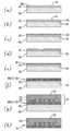
도 1(a)를 참조하면(스케일링되지 않음), 전구체 구조(10)가 개략적 및 단면도로 도시되어있다. 구조물(10)은 제1기판(12)을 포함한다. 기판(12)은 전면 또는 장치 표면 (14), 후면 (16) 및 최 외각 가장자리(edge)(18)를 갖는다. 기판(12)은 임의의 형상일 수 있지만, 일반적으로 원형 형상일 수 있다. 바람직한 제1기판(12)은 그것들의 장치 표면이 집적회로, MEMS, 마이크로 센서, 전력반도체, 발광 다이오드, 광자회로, 인터포저, 임베디드패시브 디바이스, 및 실리콘 및 실리콘-게르마늄, 갈륨 비소, 갈륨 질화물, 알루미늄 갈륨 비소, 알루미늄 인듐 갈륨 포스파이드, 및 인듐 갈륨 포스파이드로 구성된 그룹으로부터 선택된 다른 반도체 물질로부터 또는 상에 제조된 다른 마이크로 장치로 구성된 군에서 선택된 장치들(미도시)의 어레이를 포함하는 장치웨이퍼를 포함한다. 이들 장치의 표면은 일반저긍로 다음의 물질 중 하나 이상으로부터 형성된 구조(미도시)를 포함한다: 실리콘, 폴리 실리콘, 이산화 규소, 실리콘(옥시)질화물, 금속(예를 들어, 구리, 알루미늄, 금, 텅스텐, 탄탈륨), 저 유전율 유전체, 폴리머 유전체 및 다양한 금속 질화물 및 실리사이드 디바이스 표면(14)은 또한 솔더 범프; 금속 포스트; 금속 기둥; 및 규소, 폴리 실리콘, 이산화 규소, 규소(옥시)질화물, 금속, 저유전율 유전체, 중합체 유전체, 금속 질화물 및 금속 실리사이드로 이루어진 그룹으로부터 선택된 물질로부터 형성되는 구조물을 포함한다.Referring to Figure 1(a) (not scaled),
도 1(a)에 도시된 바와 같이, 본 발명에 따른 레이저 방출성 접착 조성물은 제1기판(12)에 적용되어 장치 표면(14)상에 레이저 방출 가능 접착층(20)을 형성한다. 접착층(20)은 제1기판(12)으로부터 이격된 상부표면(21)을 가지며, 바람직하게는 접착층(20)은 장치표면(14)상에 직접 형성된다(즉, 접착층(20) 및 기판(12)사이에 중간층이 없이). 접착 조성물은 임의의 공지된 적용 방법에 의해 적용될 수 있다. 하나의 바람직한 방법은 약 10초 내지 약 120초(바람직하게는 약 30초 내지 약 90초)동안 약 500rpm 내지 약 3,000rpm(바람직하게는 약 1,000rpm 내지 약 2,000rpm)의 속도로 조성물을 스핀 코팅하는 것을 포함한다.As shown in Fig. 1(a), the laser-emissive adhesive composition according to the present invention is applied to the
조성물을 적용한 후, 바람직하게는 약 120℃ 내지 약 250℃의 온도, 더욱 바람직하게는 약 150℃ 내지 약 200℃의 온도로, 및 약 60초 내지 약 10분(바람직하게는 약 120초 내지 약 5 분)의 시간 동안 가열된다. 중요하게는, 이 가열 동안 가교가 거의 또는 전혀 일어나지 않는다. 다시 말해서, 생성된 접착층(20)은 바람직하게는 열가소성이다.After applying the composition, preferably at a temperature of about 120°C to about 250°C, more preferably at a temperature of about 150°C to about 200°C, and from about 60 seconds to about 10 minutes (preferably from about 120 seconds to about 5 minutes). Importantly, little or no crosslinking occurs during this heating. In other words, the resulting
일부 실시 형태에서, 사용되는 조성물에 따라 접착층(20)을 다단계 베이크 공정에 적용하는 것이 바람직하다. 또한, 일부 경우에, 접착층(20)이 제1기판(12)상에 여러 단계로 "빌트(built)"되도록, 상기 적용 및 베이크 공정은 조성물의 추가 분취량에서 반복될 수 있다.In some embodiments, it is desirable to apply the
추가의 구체예에서, 본 발명에 따른 레이저 방출성 접착 조성물은 유동성 조성물로서 도포되기보다는 미리 형성된 건조 필름으로 형성될 수 있다. 이 경우, 조성물은 지지되지 않더라도 형태가 무너지거나 형태가 변하지 않는(지지력 또는 에너지의 부재) 지지되지 않는 자립형 필름으로 형성된다. 이어서 이 필름은 제1기판(12)에 접착되어 도 1(a)에 도시된 레이저 이형성 접착 조성물(20)을 형성할 수 있다.In a further embodiment, the laser emissive adhesive composition according to the invention can be formed from a preformed dry film rather than applied as a flowable composition. In this case, the composition is formed of a self-supporting self-supporting film that does not collapse in shape or does not change shape (in the absence of support or energy) even if it is not supported. Subsequently, the film may be adhered to the
접착층(20)의 형성 방법에 관계없이, 평균 두께(5군데에서 측정)는 약 1μm 내지 약 100μm, 보다 바람직하게는 약 5μm 내지 약 50μm, 더욱더 바람직하게는 약 1μm 내지 약 30μm이어야 한다. 본 원에 사용된 두께는 임의의 필름 두께 측정 도구를 사용하여 측정될 수 있으며, 하나의 바람직한 도구는 적외선 간섭계, 예컨대 SUSS Microtec 또는 Foothill에 의해 판매되는 것들이다.Regardless of the method of forming the
접착층(20)은 또한 총 두께 변동("TTV")이 낮아야 하며, 이는 접착층(20)이 가장 두껍고 가장 얇은 지점이 서로 크게 다르지 않음을 의미한다. TTV는 바람직하게는 필름상의 다수의 지점 또는 위치, 바람직하게는 적어도 약 50점 또는 약 50점, 더욱 바람직하게는 적어도 약 100점 또는 약 100점, 및 더욱 바람직하게는 적어도 약 1,000점, 또는 약 1,000점인 군데에서 두께를 측정함으로써 계산된다. 이 지점에서 얻은 최고 두께 측정과 최저 두께 측정간의 차이는 해당 특정 층에 대한 TTV 측정으로 지정된다. 일부 TTV측정 사례에서, 가장자리(edge) 배제 또는 이상 치는 계산에서 제거될 수 있다. 이 경우 포함된 측정의 수는 백분율로 표시된다. 즉, TTV가 97% 포함된 경우 최고 및 최저 측정의 3%가 제외되고 3%는 최고 값과 최저(즉, 각각 1.5%)로 균등하게 분할된다. 바람직하게는, 상기 언급된 TTV범위는 측정의 약 95% 내지 약 100%, 보다 바람직하게는 측정의 약 97% 내지 약 100%, 더욱더 바람직하게는 측정의 약 100%를 사용하여 달성된다.The
절대 수(예를 들어, 5μm)의 관점에서 낮은 TTV 이외에, 접착층(20)의 평균 막 두께에 대한 TTV는 낮아야 한다. 따라서, 접착층(20)은 접착층(20)의 평균 두께의 약 25%미만, 바람직하게는 평균 두께의 약 10% 미만, 더욱 바람직하게는 평균 두께의 약 5%미만의 블랭크 기판 상의 TTV를 가져야 한다. 예를 들어, 접착층(20)의 평균 두께가 50μm인 경우, 허용되는 최대 TTV는 약 12.5μm 이하(50μm의 약 25% 미만), 바람직하게는 약 5μm이하(50μm의 약 10% 미만), 및 보다 바람직하게는 약 2.5μm이하(50μm의 약 5%미만)일 것이다. In addition to the low TTV in terms of absolute number (eg, 5 μm), the TTV for the average film thickness of the
부가적으로, 레이저 방출성 접착층(20)은 원하는 기판과 강한 접착 결합을 형성할 것이다. ASTM D4541/D7234에 의해 결정된 바와 같이, 약 50 psig 초과, 바람직하게는 약 80 psig 내지 약250psig, 및 보다 바람직하게는 약 100psig 내지 약 150psig의 접착 강도를 갖는 것이 접착층(20)으로서 사용하기에 바람직할 것이다.Additionally, the laser emissive
접착층(20)은 약 0.008 이상, 바람직하게는 약 0.05이상, 더욱 바람직하게는 약 0.1 이상, 및 더욱 더 바람직하게는 약 0.1 내지 0.4의 k값을 가질 것이다.The
제2전구체 구조(22)는 또한 도 1(a)에 개략적 및 단면도로 도시되어 있다. 제2전구체 구조(22)는 제2기판(24)을 포함한다 이 실시예에서, 제2기판(24)은 캐리어 웨이퍼(carrier wafer)이다. 즉, 제2기판(24)은 전면 또는 캐리어 표면(26), 후면(28) 및 최외각 가장자리(edge)(30)를 갖는다. 제2기판(24)은 임의의 형상일 수 있지만, 전형적으로 형상이 원형이고 제1기판(12)과 유사하게 크기가 정해질 것이다. 바람직한 제2기판(24)은 투명 유리 웨이퍼 또는 레이저 에너지가 캐리어 기판을 통과하게 하는 임의의 다른 투명(레이저 에너지로)기판을 포함한다. 특히 바람직한 유리 캐리어 웨이퍼 중 하나는 Corning® EAGLE XG® 유리 웨이퍼이다.The
이어서, 구조들(10 및 22)은 대면하는(face-to-face) 관계로 함께 가압되어, 접착층(20)의 상부 표면(21)은 제 2기판(24)의 전면 또는 캐리어 표면(26)과 접촉한다(도 1(b)). 가압하는 동안, 충분한 압력과 열이 충분한 시간 동안 가해져서 2개의 구조물(10, 22)이 함께 결합하여 결합된 스택(34)을 형성한다. 접착 파라미터는 접착층(20)이 형성되는 조성물에 따라 변할 수 있지만, 이 단계 동안의 전형적인 온도는 약 150℃ 내지 약 250℃, 및 바람직하게는 약 180℃ 내지 약 220℃ 범위이며, 전형적인 압력은 약 1,000N 내지 약 25,000N, 및 바람직하게는 약 3,000N 내지 약 20,000N이며, 시간은 약 30초 내지 약 20분, 및 바람직하게는 약 3분 내지 약 10분 동안이다.Subsequently, the
접착된 스택(34)은 총 평균 두께의 약 10% 미만, 바람직하게는 총 평균 두께의 약 5% 미만 (스택(34)을 5곳의 위치에서 측정), 더욱 더 바람직하게는 접착된 스택(34)의 총 두께의 약 3%미만의 TTV를 가져야 한다. 즉, 접착된 스택(34)의 평균 두께가 100μm인 경우, 약 10% 미만의TTV는 약 10μm이하일 것이다.The glued
제1기판(12)는 이제 안전하게 취급될 수 있고, 제2기판(24)에 접착되지 않으면 제1기판(12)를 손상시킬 수 있는 추가 처리를 받을 수 있다. 따라서, 구조는 이들 후속 처리 단계 동안 발생하는 임의의 화학 물질의 침투없이, 백그라인딩, 화학-기계적 연마("CMP"), 에칭, 금속 증착(즉, 금속화), 유전체 증착, 패턴화(예를 들어, 포토리소그래피(photolithography, 에칭을 통해(via etching)), 어닐링, 재분배층 형성 및 이들의 조합과 같은 후면 과정을 기판(12 및 24)의 분리가 발생하지 않고 안전하게 수행할 수 있다. 접착층(20)은 이러한 공정을 견뎌낼 수 있을 뿐만 아니라, 약 300℃이하, 바람직하게는 약 150℃ 내지 약 280℃, 더욱 바람직하게는 약 180℃ 내지 약 250℃의 가공 온도에서 견딜 수 있다.The
처리가 완료되면, 레이저 방출성 접착층(20)의 전부 또는 일부를 분해하거나 제거하기 위해 레이저를 사용하여 기판(12 및 24)을 분리할 수 있다. 적합한 레이저에는 UV레이저가 포함되고, 파장은 바람직하게는 약 200nm 내지 약 400nm, 및 바람직하게는 약 300nm 내지 약 360mn의 파장의 UV레이저를 포함한다. 레이저 방출성 접착층을 분리하기 위해, 레이저는 전체 웨이퍼를 노출시키기 위해 스네이크형 패텬으로 캐리어 웨이퍼의 표면을 가로질러 스캐닝된다. 예시적인 레이저 분리 도구에는 SUSS Micro TecLambda STEEL 2000레이저 분리기, EVG850DB 자동 분리 시스템, 및 Kingyoup LD-Automatic 200/300 레이저 분리기가 포함된다. 웨이퍼는 바람직하게는 약 40x40μm 내지 약 12.5x4mm의 필드 크기를 갖는 레이저 스폿(spot)에 의해 스캐닝된다. 기판을 분리하기에 적합한 플루언스는 약 100 mJ/cm2 내지 약 400mJ/cm2, 및 바람직하게는 약 150 mJ/cm2 내지 350 mJ/cm2 이다. 기판을 분리하기에 적합한 전력은 약 2
W 내지 약 6W, 및 바람직하게는 약 3W 내지 약 4W이다.When the treatment is completed, the
레이저 노출 후, 기판(12 및 24)은 쉽게 분리될 것이다. 분리 후, 임의의 나머지 접착층(20)은 플라즈마 에칭 또는 접착층(20)을 용해시킬 수 있는 용매로 제거될 수 있다. After laser exposure, the
상기 실시예에서, 레이저-이탈성 접착층(20)은 디바이스 웨이퍼인 제1기판(12)상에 도시되어 있다. 이 기판/층 방식이 반대로 될 수 있다는 것이 이해될 것이다. 즉, 접착층(20)은 제2기판(24)(즉, 캐리어 웨이퍼)상에 형성될 수 있다. 전술한 것과 동일한 조성 및 처리 조건이 본 실시예에 적용될 것이다.In this embodiment, a laser-leaving
특히 바람직한 실시예에서, 접착층(20)은 도 1에 도시된 바와 같이 기판(12 및 24)사이의 유일한 층이다. 그러나, 대안적인 실시예에서, 접착층(20)은 추가적인 접착 재료, 구조적 지지층, 라미네이션 보조층, 타이층(초기 기판에 대한 접착을 위해), 오염제어층 및 세정층과 함께 사용될 수 있는 것이 이해할 것이다. 바람직한 구조 및 응용기술은 응용 및 과정 흐름에 따라 결정된다.In a particularly preferred embodiment, the
이 대안적인 다층 실시예의 예시가 도 2에 도시되어 있으며, 여기서 도 1의 번호와 동일한 번호는 동일한 부분을 나타낸다. 도 2 실시예에서, 본 발명의 접착 조성물은 도 2(a)에 도시된 바와 같이, 캐리어 표면(26)상에 접착층(20)을 형성하기 위해 제2기판(24)에 도포되어, 구조(22')를 형성한다. 대안적으로, 구조(22')는 이미 형성된 상태로 제공될 수 있다. 레이저 방출성 접착층(20)을 형성하는데 사용된 본 발명의 접착 조성물과는 다른 제2조성물이 층(32)을 형성하기 위해 제 1기판(12)의 디바이스 표면(14)에 도포된다. 층(32)은 제1기판(12)으로부터 떨어진 상부 표면(34) 및 제1기판(12)에 인접한 하부 표면(36)을 갖는다. 일 실시예에서, 층(32)은 다층 접착 방식이 바람직한 경우에 사용하기 위한 제2접착층이다. 이러한 경우에, 제2접착층(32)의 접착강도는 레이저 이형성 접착층(20)의 접착강도보다 큰(강한)것이 바람직하다. 특히, 제2접착층(32)의 접착강도는 레이저 이형성 접착층(20)의 접착 강도의 약 1.2배 이상, 바람직하게는 약 1.5배 이상, 더욱 바람직하게는 약 1.7 내지 약 4배이다. 제1 및 제2기판(12, 24)의 분리는 전술한 바와 같이 수행될 수 있다.An example of this alternative multi-layer embodiment is shown in FIG. 2, where the same numbers as in FIG. 1 denote the same parts. In the FIG. 2 embodiment, the adhesive composition of the present invention is applied to the
대안적으로, 이 기판/층 방식은 다층방식으로 역전될 수 있다. 즉, 층(32)은 제2기판(24)(캐리어 웨이퍼)상에 형성될 수 있는 반면, 본 발명의 레이저 방출성 접착층(20)은 제1기판(12)(디바이스 웨이퍼)상에 형성된다. 이 경우, 층(32)(접착층인지 여부에 관계없이)은 레이저 에너지가 제2기판(24)을 통과한 후 레이저 에너지가 통과할 수 있도록 선택될 것이다. 따라서, 전술한 바와 같이, 레이저 에너지가 레이저 방출 가능 접착층(20)과 접촉하고 분해를 야기하게 한다.Alternatively, this substrate/layer scheme can be reversed in a multilayer scheme. That is, the
2.2. 빌드-업 레이어 구현(Build-Up Layer Embodiment)Build-Up Layer Embodiment
추가의 구체예에서, 본 발명의 레이저 방출성 조성물은 재분배층("RDL")형성을 위한 빌드-업 층으로서, 특히 웨이퍼 또는 패널 레벨 공정에서 RDL-제1/칩-라스트 패키징에 사용될 수 있으며, 이는 패키징 중 알려진 양호한 다이 손실을 최소화하거나 피하는데 좋다. 이러한 과정 중 하나의 개략도가 도 3에 도시되어 있다. In a further embodiment, the laser emissive composition of the present invention can be used for RDL-first/chip-last packaging as a build-up layer for forming a redistribution layer ("RDL"), especially in wafer or panel level processes. This is good for minimizing or avoiding known good die losses during packaging. A schematic diagram of one of these processes is shown in FIG. 3.
전술한 바와 같은 레이저 방출성 결합 또는 빌드-업 조성물은 캐리어 기판(40)의 상부표면(38)에 적용되어 도 3(a)에 도시된 바와 같이 캐리어 표면(38) 상에 레이저 방출 가능한 빌드-업 층(42)을 형성한다. 빌드-업 층(42)은 처리조건 및 결과적인 특성을 포함하여 상기 임시 결합 실시예와 관련하여 설명된 임의의 방법에 따라 형성된다. 빌드-업 층(42)은 캐리어 기판(40)으로부터 떨어진 상부표면(44)을 가지며, 바람직하게는 빌드-업층(42)은 캐리어 기판(40)의 상부 표면 (38) 상에 직접 형성된다(즉, 빌드-업 층(42)사이에 어떠한 중간층도 없음).The laser-emissive bonding or build-up composition as described above is applied to the
다음으로, 종래의 방법에 따라 시드층(46)이 상부 표면(44) 상에 증착된다(도 3(b)). 시드층(46)은 포토레지스트로 코팅되고, 다시 공지된 방법에 따라 패턴화 되고 전기 도금되어도 도 3(c)에 도시된 구조를 형성할 수 있다. 도 3(d)를 참조하면, 포토 레지스트를 스트리핑하고 금속을 에칭한 후, 유전체층의 코팅, 패터닝 및 경화를 수행한다. 이는 도 3(e)를 참조하면, 포토레지스트를 스트리핑하고 금속을 에칭한 후, 유전체 층의 코팅, 패터닝 및 경화를 수행한다. 이는 도 3(e)에 도시된 바와 같이 제1RDL(48)을 형성시킨다. 도 3(b) 내지 도 3(e)의 단계들은 다수의 RDLs을 생성하기 위해 필요에 따라 여러 번 반복 될 수 있다(도 3(f)에 도시된 실시예에서, 48 (a)-(d), 즉 4개의 RDL).Next, a
도 3(g)를 참조하면, 원하는 수의 RDL이 형성된 후에, 솔더볼(50)이 다시 종래의 방법에 따라 최상위(마지막 형성된) RDL에 부착된다. 다이(52)는 솔더볼(50)에 접착된 후, 종래의 에폭시 몰딩층(54)의 적용 및 분쇄에 의해 팬-아웃 웨이퍼 레벨 패키지 구조(56)를 형성한다. 마지막으로, 레이저 에너지는 레이저-릴리스 가능 빌드-업층(42)의 전부 또는 일부를 분해하거나 제거하기 위해 전술한 레이저 분리조건에 따라 캐리어 기판(40)에 인가된다. 레이저 적용 후, 캐리어 기판(40)은 팬-아웃 웨이퍼 레벨 패키지 구조(56) (도 3(h))로부터 분리될 것이며, 남아있는 빌드-업 층(42)은 용매에 의해 제거된다.Referring to FIG. 3(g), after the desired number of RDLs is formed, the
전술한 팬-아웃 웨이퍼 레벨 패키지 구조를 형성하기 위한 공정은 본 발명의 조성물을 빌드-업 층으로서 사용하여 수행될 수 있는 이러한 유형의 공정의 하나의 예일 뿐이며, 이 과정의 변형은 사용자 요구에 따라 이루어질 수 있다. 예를 들어, RDL층의 수는 솔더볼 및 다이의 수 및 위치뿐만 아니라 필요에 따라 변할 수 있다. 이러한 구성은 본 기술 분야의 숙련자에 의해 이해되고 맞춤화될 것이다.The above-described process for forming the fan-out wafer level package structure is only one example of this type of process that can be performed using the composition of the present invention as a build-up layer, and variations of this process can be made according to user needs. It can be done. For example, the number of RDL layers can vary as needed, as well as the number and location of solder balls and dies. This configuration will be understood and customized by those skilled in the art.
본 발명의 다양한 구체 예의 추가 장점은 본 원의 개시 및 하기 실시예를 검토할 때 당업자에게 명백할 것이다. 본 명세서에 기술된 다양한 실시예는 본 명세서에서 달리 지시되지 않는 한 상호 배타적일 필요 없이 이해될 것이다. 예를 들어, 일 실시예에서 설명되거나 도시된 특징은 다른 실시예에도 포함될 수 있지만, 반드시 포함되는 것은 아니다. 따라서, 본 발명은 여기에 설명된 특정 실시예의 다양한 조합 및/또는 통합을 포함한다.Additional advantages of various embodiments of the invention will be apparent to those skilled in the art upon reviewing the disclosure and the examples below. Various embodiments described herein will be understood to be mutually exclusive, unless otherwise indicated herein. For example, features described or illustrated in one embodiment may be included in other embodiments, but are not necessarily included. Accordingly, the present invention includes various combinations and/or integrations of the specific embodiments described herein.
본 원에 사용된 어구 "및/또는"은 둘 이상의 항목의 목록에서 사용될 때, 나열된 항목 중 어느 하나가 그 자체로 이용될 수 있거나 또는 나열된 항목 중 둘 이상의 임의의 조합이 사용될 수 있음을 의미한다. 예를 들어, 조성물이 성분 A, B 및/또는 C를 함유하거나 배제하는 것으로 기술되는 경우, 조성물은 A를 단독으로 함유하거나 배제할 수 있고; B 단독; C단독; A 및 B의 조합; A및 C의 조합; B및 C의 조합; 또는 A, B 및 C의 조합일 수 있다.The phrase “and/or” as used herein, when used in a list of two or more items, means that either of the listed items can be used by itself or any combination of two or more of the listed items can be used. . For example, if the composition is described as containing or excluding components A, B and/or C, the composition may contain or exclude A alone; B alone; C alone; Combination of A and B; Combination of A and C; Combination of B and C; Or A, B and C.
본 설명은 또한 수치 범위를 사용하여 본 발명의 다양한 실시예와 관련된 특정 파라미터를 정량화한다. 수치범위가 제공될 때, 그러한 범위는 범위의 더 낮은 값만을 언급하는 청구 제한 및 범위의 상위 값만을 언급하는 청구 제한에 대한 문자적 지원을 제공하는 것으로 해석되어야 한다. 예를 들어, 약 10 내지 약 100의 개시된 수치 범위는 "약 10 보다 큰"을 언급하는 청구(상한없이) 및 "약 100보다 작은"을 언급하는 청구(하한없이)에 대한 문자적 지원을 제공한다.This description also uses numerical ranges to quantify specific parameters related to various embodiments of the invention. When a numerical range is provided, such range should be construed as providing literal support for claims limits that refer only to the lower value of the range and claims limits that refer only to the upper value of the range. For example, the disclosed numerical ranges of about 10 to about 100 provide literal support for claims (without the upper limit) referring to "greater than about 10" and claims (without the lower limit) referring to "less than about 100". do.
도 1은 본 발명에 따른 바람직한 임시 접착방법을 도시한 개략도의 단면도이다.
도 2는 도 1의 실시예에 대한 변형을 도시한 개략도의 단면도이다.
도 3은 본 발명에 따른 재분배층 형성을 도시한 개략도이다.
도 4는 실시예 2에서 시험된 중합체의 TGA(공기 중)를 도시한 그래프이다.
도 5는 실시예 2에서 시험된 중합체 1의 TGA(질소 중)를 도시한 그래프이다.
도 6은 실시예 4에서 시험된 바와 같이 제형 1에 의해 생성된 접착선의 SUSS크로크로다일 사진이다. 및
도 7은 실시예 6에 기술된 바와 같이 308nm에서 분리된 블랭크 장치이다.1 is a cross-sectional view of a schematic diagram showing a preferred temporary bonding method according to the present invention.
FIG. 2 is a cross-sectional view of a schematic diagram showing a modification to the embodiment of FIG. 1.
3 is a schematic diagram showing the formation of a redistribution layer according to the present invention.
4 is a graph showing the TGA (in air) of the polymer tested in Example 2.
FIG. 5 is a graph showing TGA (in nitrogen) of
FIG. 6 is a SUSS crocodile photograph of the bond line produced by
FIG. 7 is a blank device separated at 308 nm as described in Example 6.
하기 실시예는 본 발명에 따른 방법을 제시한다. 그러나, 이들 실시예는 예시로서 제공되며, 본 발명의 전체 범위를 제한하는 것으로 간주되어서는 안된다는 것을 이해해야한다.The following examples show the method according to the invention. However, it should be understood that these examples are provided by way of illustration and should not be regarded as limiting the entire scope of the invention.
실시예 1Example 1
레이저 분리용 중합체 1Polymers for
이 절차에서, 13.07 g의 4,4'-디하이드록시벤조페논(TCI America, Portland, OR), 20.76 g의 비스페놀A 디글리시딜에테르(D.E.R.TM 332, Sigma-Aldrich, St. Louis, MO)및 0.84g의 에틸트리페닐포스포리움브로마이드(Sigma-Aldrich, St. Louis, MO)를 3구 둥근 바닥 플라스크에서 65.33g의 사이클로펜타논(Sigma-Aldrich, St. Louis, MO)에 용해시켰다. 혼합물을 140℃에서 12시간동안 반응시켰다. 생성된 중합체 1을 1,000g의 에탄올(Sigma-Aldrich, St. Louis, MO)에 침전시킨 후, 진공하에 80℃에서 밤새 건조시켰다.In this procedure, 13.07 g of 4,4'-dihydroxybenzophenone (TCI America, Portland, OR), 20.76 g of bisphenol A diglycidyl ether (DER TM 332, Sigma-Aldrich, St. Louis, MO ) And 0.84 g of ethyl triphenylphosphorium bromide (Sigma-Aldrich, St. Louis, MO) were dissolved in 65.33 g of cyclopentanone (Sigma-Aldrich, St. Louis, MO) in a three-neck round bottom flask. . The mixture was reacted at 140° C. for 12 hours. The resulting
이어서, 정제된 중합체 30g을 시클로펜타논 70g에 용해시키고 하루동안 교반하여 균질한 용액을 수득하였다. 생성된 중합체 1을 0.2μm메시너필터(messiner filter)를 통해 여과하였다.Subsequently, 30 g of the purified polymer was dissolved in 70 g of cyclopentanone and stirred for one day to obtain a homogeneous solution. The resulting
이 실시예에서 일어나는 반응은 다음과 같다:The reactions occurring in this example are as follows:

![]()
![]()
실시예 2Example 2
중합체 1의 성질Properties of
열 중량 분석(TGA)은 공기 및 질소 중에서 10℃/min 램프에서 수행되었다. 결과는 도 4및 도 5에 도시되어 있다. 중합체는 공기에서 약 350℃, 질소에서 360℃의 비교적 높은 초기 분해 온도를 나타냈다. Thermogravimetric analysis (TGA) was performed in air and nitrogen in a 10° C./min lamp. The results are shown in FIGS. 4 and 5. The polymer showed a relatively high initial decomposition temperature of about 350°C in air and 360°C in nitrogen.
중합체 1은 완전히 특성화 되었고, 특성화 데이터는 표 1에 제시되어 있다. 중량 평균 분자량(Mw) 및 다분산도("PDI")를 용리 용매로서 THF를 사용하여 겔투과크로마토그래피(GPC)를 사용하여 측정하였다. 유리전이온도(Tg)는 25℃에서 250℃의 질소 환경에서 시차주사열량측정(DSC)으로 감지되었다. TA 인스트루먼츠의 레오미터를 사용하여 재료의 유동학적 특성(용융 점도 포함)을 시험하였다. 샘플을 250℃에서 로딩하였고, 유변학적 특성을 250℃ 내지 50℃로 기록하였다.

표 1. 중합체 1의 특성Table 1. Properties of
유변학 데이터는 중합체 1재료가 이 온도에서의 낮은 용융 점도로 인해 약 200℃의 우수한 접착 라인을 얻기 위해 열 압착 접착 공정과 함께 사용될 수 있음을 보여주었다. Rheological data showed that the
실시예 3Example 3
중합체 1의 광학 테스트Optical test of
가변 각도 분광 엘립소 미터(VASE)를 사용하여 중합체 1에 대한 광학 상수(n & k)를 결정하였다. 표 2는 두개의 다른 파장에서 샘플의 광학 상수 n 및 k를 보여준다. 중합체 1은 308nm에서 0.2의 k값으로 매우 우수한 흡광도를 나타내었지만, k값 0.008에서 355nm에서 우수하지 않았다. 308nm에서의 이러한 높은 k는 또한 중합체 1이 이 파장에서 우수한 레이저 분리 성능을 가질 가능성이 있음을 나타냈다.The optical constant (n & k) for

표 2. 중합체 1의 광학 상수Table 2. Optical constants of
실시예 4Example 4
제형 1을 사용한 접착Adhesion with
본 실시예에서는, 캐리어 웨이퍼로서 8인치 유리 웨이퍼 상에 실시예 1의 제형 16μm를 코팅하였다. 이 코팅은 30초 동안 3,000rpm/s의 가속도로 1,000rpm에서 스핀 코팅에 의해 달성되었다. 이어서, 캐리어 웨이퍼를 50℃에서 3분동안, 120℃에서 3분 동안 및 200℃에서 3분동안 베이킹하였다. 코팅된 캐리어 웨이퍼는 EVG®510접착 시스템(EV 그룹)에서 진공(<5 mbar)하에 230℃, 2000N에서 3분 동안 접착함으로써 8인치 Si웨이퍼에 접착되었다. 결합 쌍은 Precitec센서를 사용하고 회전 기판을 측정하고 웨이퍼 표면에서 수백 또는 수천점을 측정할 수 있는 Chrocdail IR간섭계(SUSS Micro Tec SE)로 스캔되었다. 어떠한 공극도 검출되지 않았으며(도 6 참조), 재료는 97%의 측정값을 사용하여 최소 총 두께 변동("TTV"- total thickness variation)이 1.72μm인 양호한 결합선(16.7μm 두께)을 나타냈다. In this example, 16 μm of the formulation of Example 1 was coated on an 8 inch glass wafer as a carrier wafer. This coating was achieved by spin coating at 1,000 rpm with an acceleration of 3,000 rpm/s for 30 seconds. The carrier wafer was then baked at 50°C for 3 minutes, at 120°C for 3 minutes and at 200°C for 3 minutes. The coated carrier wafer was bonded to an 8 inch Si wafer by bonding at 230° C., 2000 N for 3 minutes under vacuum (<5 mbar) in an EVG ® 510 adhesive system (EV group). The binding pair was scanned with a Chrocdail IR interferometer (SUSS Micro Tec SE) using a Precitec sensor, measuring a rotating substrate and measuring hundreds or thousands of points on the wafer surface. No voids were detected (see FIG. 6), and the material exhibited a good bond line (16.7 μm thickness) with a minimum total thickness variation (“TTV”—total thickness variation) of 1.72 μm using a measurement of 97%.
실시예 5Example 5
공식 1을 사용한 웨이퍼 희석Wafer
실시예 4에 기술된 바와 같이 제조된 6개의 접착된 웨이퍼 쌍은 60μm의 목표 두께를 갖는 분쇄기/ 연마기(DGP8761, Disco Corporation)를 사용하여 분쇄 박화 시험을 받았다. 웨이퍼는 1μm/s ~ 5μm/s의 제거 속도로 대략 90μm까지 연마된 다음 0.2μm/s ~ 0.4μm/s의 제거속도로 62μm까지 더 연마되었다. 이어서 웨이퍼를 연마해서 60μm 최종 목표 두께를 달성하기 위해 1μm/min의 제거 속도로 2μm더 얇게 만들었다. 표 3은 6개의 웨이퍼 쌍의 세부 데이터를 보여준다. 접착 라인의 두께 및 TTV는 그라인딩 전의 수와 일치하여, 그라인딩 공정 동안 접착 재료의 기계적 안정성을 나타낸다. 얇은 Si 웨이퍼는 또한 우수한 TTV로 목표 두께를 달성했다. 또한, 얇은 웨이퍼 쌍에 대해 250℃에서 30분 동안 질소 오븐에서 베이킹하여 열 시뮬레이션을 수행하였다. 웨이퍼에 대해 심각한 결함이 관찰되지 않았다.The six bonded wafer pairs prepared as described in Example 4 were subjected to a pulverization thinning test using a grinder/grinder (DGP8761, Disco Corporation) with a target thickness of 60 μm. The wafer was polished to approximately 90 μm at a removal rate of 1 μm/s to 5 μm/s and then further polished to 62 μm at a removal rate of 0.2 μm/s to 0.4 μm/s. The wafer was then polished to 2 μm thinner with a removal rate of 1 μm/min to achieve a final target thickness of 60 μm. Table 3 shows detailed data of six wafer pairs. The thickness of the adhesive line and the TTV are consistent with the number before grinding, indicating the mechanical stability of the adhesive material during the grinding process. The thin Si wafer also achieved its target thickness with an excellent TTV. In addition, a thin wafer pair was baked in a nitrogen oven at 250° C. for 30 minutes to perform a thermal simulation. No serious defects were observed for the wafer.

표 3. 연삭 전후의 접착된 웨이퍼 쌍Table 3. Bonded wafer pairs before and after grinding
실시예 6Example 6
제형1을 사용한 레이저 분리 및 세척Laser separation and
포뮬레이션을 사용한 레이저 분리 및 세척 시장에 출시된 3가지 주요 UV-레이저 파장, SUSS ELD12 레이저 분리기(SUSS ELD12 Laser Debonder), EVG 반자동 분리 시스템(EVG Semi-Automatic Debonding System), 및 Kingyoup LD-Semi Automatic 200/300을 사용하여 접착된 웨이퍼 쌍을 성공적으로 분리했다. 3개의 분리기 각각에 대한 레이저 분리 파라미터가 표 4에 나열되어 있다. 분리된 장치 웨이퍼의 이미지가 도 7에 도시되어 있다. 장치 웨이퍼에 남아있는 잔류물은 사이클로펜타논을 사용하여 매우 잘 세척되었다. 세정 후, 웨이퍼는 잔류물 없이 녹색광 하에서 시각적으로 세정되었다.Laser separation and cleaning using formulations Three major UV-laser wavelengths on the market, SUSS ELD12 Laser Debonder, EVG Semi-Automatic Debonding System, and Kingyoup LD-Semi Automatic Bonded wafer pairs were successfully separated using 200/300 . The laser separation parameters for each of the three separators are listed in Table 4. An image of the separated device wafer is shown in FIG. 7. The residue remaining on the device wafer was cleaned very well using cyclopentanone. After cleaning, the wafer was visually cleaned under green light without residue.

표 4. 레이저 분리 매개 변수Table 4. Laser separation parameters
실시예 7Example 7
레이저 분리용 중합체 2Polymers for laser separation 2
이 실시예에서, 17.71g의 4,4'-디하이드록시벤조페논(4,4'-dihydroxybenzophenone), 30.94g의 비스페놀A 디글리시딜에테르(D.E.R.TM 332) 및 1.35g의 에틸트리페닐포스포리움 브로마이드(ethyltriphenylphosphorium bromide)는 3구 둥근바닥 플라스크에서 50 g의 시클로헥사논(Sigma-Aldrich, St. Louis, MO)에 용해되었다. 혼합물을 150℃에서 24시간동안 반응시켰다. 이어서, 57.34g의 중합체를 42.66g의 감마-부티로락톤(gamma-butyrolactone)에 용해시키고 하루 동안 교반하여 균질한 용액을 수득하였다. 생성된 제형2를 0.2μm 메시너필터를 통해 여과하였다.In this example, 17.71 g of 4,4'-dihydroxybenzophenone, 30.94 g of bisphenol A diglycidyl ether (DER TM 332) and 1.35 g of ethyltriphenylphos Porium bromide (ethyltriphenylphosphorium bromide) was dissolved in 50 g of cyclohexanone (Sigma-Aldrich, St. Louis, MO) in a 3-neck round bottom flask. The mixture was reacted at 150° C. for 24 hours. Subsequently, 57.34 g of polymer was dissolved in 42.66 g of gamma-butyrolactone and stirred for one day to obtain a homogeneous solution. The resulting formulation 2 was filtered through a 0.2 μm Messier filter.
실시예 8Example 8
제형 2를 사용한 접착Adhesion with Formulation 2
이 과정에서, 실시예 7의 21μm의 제형 2를 캐리어 웨이퍼로 8인치 유리 웨이퍼 상에 30초 동안 3,000rpm/s의 가속도로 1,000rpm으로 스핀 코팅함으로써 코팅하였다. 이어서, 캐리어 웨이퍼를 4분동안 50℃에서, 4분동안 110℃에서, 4분동안 200℃에서, 마지막으로 220℃에서 4분동안 베이킹하였다. 코팅된 캐리어 웨이퍼를 8인치 Si웨이퍼에 결합시켰다. 웨이퍼쌍을 EVG®510 bonder에서 진공(<5 mbar)하에 210℃, 2,000N에서 4분동안 접착시켰다. 육안 검사로 양호한 결합선 형성이 확인되었다.In this process, 21 μm of Formulation 2 of Example 7 was coated on a 8 inch glass wafer with a carrier wafer by spin coating at 1,000 rpm with an acceleration of 3,000 rpm/s for 30 seconds. The carrier wafer was then baked at 50°C for 4 minutes, at 110°C for 4 minutes, at 200°C for 4 minutes, and finally at 220°C for 4 minutes. The coated carrier wafer was bonded to an 8 inch Si wafer. The wafer pair was adhered in an EVG ® 510 bonder under vacuum (<5 mbar) at 210° C. and 2,000 N for 4 minutes. Good visual line formation was confirmed by visual inspection.
실시예 9Example 9
제형 2로부터 건조필름의 생성Formation of dry film from formulation 2
바코더(K303 Multicoater, RK PrintCoat Instruments Ltd, United Kingdom)를 사용하여 다음 조건 하에서 레이저 감응성 열가소성 제형 2를 50μm 폴리에틸렌테레프탈레이트(polyethylene terephthalate) 담체 필름(H950A, Nan Ya Plastics Corporation, Taiwan) 상에 캐스팅하였다: 80μm의 간격 및 분당 4미터의 속도. 용매-캐스트 필름을 핫 플레이트에서 50℃에서 5분 동안 건조시킨 다음 140℃에서 5분동안 건조시켜 독립형, 건조된, 두께 20μm의 접착필름, 폭 200mm, 및 길이300mm를 수득하였다.Laser-sensitive thermoplastic formulation 2 was cast on a 50 μm polyethylene terephthalate carrier film (H950A, Nan Ya Plastics Corporation, Taiwan) under the following conditions using a bar coder (K303 Multicoater, RK PrintCoat Instruments Ltd, United Kingdom) : 80μm interval and 4m/min speed. The solvent-cast film was dried on a hot plate at 50° C. for 5 minutes and then at 140° C. for 5 minutes to obtain a standalone, dried, 20 μm thick adhesive film, 200 mm wide, and 300 mm long.
실시예 10Example 10
드라이 필름의 라미네이션Dry Film Lamination
실시예 9에서 생성된 결합 필름을 하기 조건하에 Tamerica, TCC-2700 핫 롤 라미네이터를 사용하여 100-mm 유리 웨이퍼 상에 적층시켰다: 140℃의 롤러 온도 및 분당 0.2미터의 속도. 여분의 필름을 나이프로 다듬고, 적층 후 베이스 폴리에틸렌테레프탈레이트(polyethylene terephthalate) 필름을 박리하였다.The bonding film produced in Example 9 was laminated on a 100-mm glass wafer using Tamerica, TCC-2700 hot roll laminator under the following conditions: a roller temperature of 140° C. and a speed of 0.2 meters per minute. The excess film was trimmed with a knife, and after lamination, the base polyethylene terephthalate film was peeled off.
실시예 11Example 11
적층 유리 웨이퍼의 접착Bonding of laminated glass wafers
실시예 10에서 제조된 적층 유리 웨이퍼를 다음 조건 하에서Cee® Apogee?? bonder(Cost Effective Equipment, LLC, Rolla MO)를 사용하여 다른 100-nm 유리웨이퍼와 결합시켰다: 압반(platen) 온도 230℃, 및 3분 동안, 1,800N의 힘을 가했다. 웨이퍼 대 웨이퍼 접착 후 공극 또는 박리가 관찰되지 않았다.The laminated glass wafer prepared in Example 10 was subjected to Cee ® Apogee?? Bonder (Cost Effective Equipment, LLC, Rolla MO) was used to bond with other 100-nm glass wafers: a platen temperature of 230° C. and a force of 1,800 N was applied for 3 minutes. No voids or peeling were observed after wafer-to-wafer adhesion.
실시예 12Example 12
접착된 웨이퍼 쌍의 레이저 방출 및 청소Laser emission and cleaning of glued wafer pairs
처리 후, 접착된 유리 웨이퍼 쌍은 다음조건 하에서 355nm 레이저 분리기(LD- Semi Automatic 300, Kingyoup Enterprises Co., Ltd.)를 사용하여 분리되었다: 전력6W, 스캔속도 2m/s 및 행 간격(line pitch)40-μm. 탈 결합 후, 재사용 및 추가 처리를 위해 두 유리 웨이퍼를 GBL-사이클로헥사논(GBL-cyclohexanone) 공-용매시스템으로 스핀-세정하였다.After treatment, the bonded glass wafer pairs were separated using a 355 nm laser separator (LD-
Claims (49)
후면 및 전면을 갖는 제1기판;
상기 전면에 인접하고 폴리하이드록시에테르(polyhydroxyether)를 포함하는 접착층; 및
상기 접착층에 인접한 제 1표면을 갖는 제2기판; 및
상기 접착층을 레이저에너지에 노출시켜 상기 제1 및 제2기판의 분리를 용이하게 하는 단계를 포함하는 임시 접착 방법.
Steps to provide a stack configuration that includes:
A first substrate having a rear surface and a front surface;
An adhesive layer adjacent to the front surface and comprising a polyhydroxyether; And
A second substrate having a first surface adjacent to the adhesive layer; And
And exposing the adhesive layer to laser energy to facilitate separation of the first and second substrates.
The method of claim 1, wherein the polyhydroxy ether comprises a copolymer of diglycidyl ether and dihydroxy dye.
The method of claim 2, wherein the diglycidyl ether is bisphenol A diglycidyl ether (bisphenol A diglycidyl ether), bisphenol F diglycidyl ether (bisphenol F diglycidyl ether), 1,4-cyclohexanedimethanol di Glycidyl ether (1,4-cyclohexanedimethanol diglycidyl ether), resorcinol diglycidyl ether, bisphenol A propoxylate diglycidyl ether, ethylene glycol diglycidyl ether Diethylene ether (ethylene glycol diglycidyl ether), 1,4-cyclohexane dimethanol diglycidyl ether (1,4-cyclohexandimethanol diglycidyl ether), glycerol diglycidyl ether (glycerol diglycidyl ether), 1,4-butanediol di Glycidyl ether (1,4-butanediol diglycidyl ether), neopentyl glycol diglycidyl ether, 1,3-butanediol diglycidyl ether (1,3-butanediol diglycidyl ether), 1 ,3-bis(3-glycidoxypropyl)tetramethyldisiloxane (1,3-bis(3-glycidoxypropyl)tetramethyldisiloxane), and a method selected from the group consisting of combinations thereof.
The method of claim 2, wherein the dihydroxy dye is 4,4'-dihydroxybenzophenone (4,4'-dihydroxybenzophenone), dihydroxy chalcone dyes (dihydroxy chalcone dyes), 4-[(2-phenylhydride Lazono)methyl]resorcinol (4-[(2-phenylhydrazono)methyl]resorcinol), dihydroxyazobenzene, dihydroxyanthraquinone, 2,2'-methylenebis[6-( Benzotriazol-2-yl)-4-tert-octylphenol](2,2'-methylenebis[6-(benzotriazol-2-yl)-4- tert- octylphenol]), curcumin, curcumin derivatives ( curcumin derivatives), and combinations thereof.
The method of claim 1, wherein the adhesive layer is a thermoplastic layer.
The method of claim 1, wherein the exposure is performed at a dose of about 200 mJ/cm 2 to about 400 mJ/cm 2 .
The method of claim 1, wherein providing the stack comprises forming the adhesive layer on the front side.
The method of claim 7, wherein the forming step includes applying a flowable binding composition to the front surface, and the flowable composition comprises a polyhydroxyether dispersed or dissolved in a solvent system.
9. The method of claim 8, wherein the composition further comprises heating at a temperature of about 120°C to about 250°C for about 60 seconds to about 10 minutes to form the adhesive layer.
The method of claim 7, wherein the forming step comprises applying a freestanding film containing polyhydroxyether to the front surface to form the adhesive layer.
11. The method of claim 10, wherein the applying step comprises the step of adhering the standalone film to the front side.
(1)집적회로로 구성된 그룹으로부터 선택된 장치들의 어레이를 포함하는 장치 표면; MEMS; 마이크로 센서; 전력반도체; 발광 다이오드; 광자회로; 인터포저; 임베디드패시브 디바이스; 및 실리콘, 실리콘-게르마늄, 갈륨 비소 및 질화 갈륨 상에 또는 그로부터 제조된 마이크로디바이스; 및
(2)하기로 이루어진 군으로부터 선택된 하나 이상의 구조를 포함하는 장치 표면:
솔더 법프; 금속포스트; 금속기둥; 및 규소, 폴리실리콘, 이산화 규소, 규소(옥시)질화물, 금속, 저유전율 유전체, 중합체 유전체, 금속 질화물 및 금속 실리사이드로 이루어진 그룹으로부터 선택된 물질로부터 형성되는 방법.
According to claim 1, One of the front surface and the first surface;
(1) a device surface comprising an array of devices selected from the group consisting of integrated circuits; MEMS; Micro sensor; Power semiconductors; Light emitting diodes; Photon circuit; Interposer; Embedded passive devices; And microdevices made on or from silicon, silicon-germanium, gallium arsenide and gallium nitride; And
(2) a device surface comprising at least one structure selected from the group consisting of:
Solder soap; Metal posts; Metal columns; And a material selected from the group consisting of silicon, polysilicon, silicon dioxide, silicon (oxy) nitride, metal, low dielectric constant, polymer dielectric, metal nitride and metal silicide.
The method of claim 1, wherein one of the first and second substrates comprises glass or other transparent material.
The method of claim 1, wherein the first and second substrates are separated by backgrinding, chemical-mechanical polishing, etching, metallization, dielectric deposition, patterning, passivation, annealing, redistribution layer formation, and combinations thereof. And further comprising performing a process selected from the group consisting.
The method of claim 1, wherein the adhesive layer is the only layer between the first substrate and the second substrate.
According to claim 1, The adhesive layer has a first adhesive force, the stack further comprises a second adhesive layer between the first substrate and the second substrate, the second adhesive layer has a greater adhesive force than the first adhesive force How to have.
후면 및 전면을 갖는 제1기판;
상기 전면에 인접하고, 폴리하이드록시에테르를 포함하는 접착층; 및
상기 접착층에 인접한 제1표면을 가지며, 상기 전면 및 상기 제1표면 중 적어도 하나는 장치 표면인 제2기판을 포함하는, 구조물.
As a microelectronic structure:
A first substrate having a rear surface and a front surface;
An adhesive layer adjacent to the front surface and comprising a polyhydroxy ether; And
A structure having a first surface adjacent to the adhesive layer, wherein at least one of the front surface and the first surface comprises a second substrate that is a device surface.
18. The microelectronic structure of claim 17, wherein the polyhydroxyether comprises a copolymer of diglycidyl ether and dihydroxy dye.
The method of claim 18, wherein the diglycidyl ether is bisphenol A diglycidyl ether (bisphenol A diglycidyl ether), bisphenol F diglycidyl ether (bisphenol F diglycidyl ether), 1,4-cyclohexanedimethanol di Glycidyl ether (1,4-cyclohexanedimethanol diglycidyl ether), resorcinol diglycidyl ether, bisphenol A propoxylate diglycidyl ether, ethylene glycol diglycidyl ether Diethylene ether (ethylene glycol diglycidyl ether), 1,4-cyclohexane dimethanol diglycidyl ether (1,4-cyclohexandimethanol diglycidyl ether), glycerol diglycidyl ether (glycerol diglycidyl ether), 1,4-butanediol di Glycidyl ether (1,4-butanediol diglycidyl ether), neopentyl glycol diglycidyl ether, 1,3-butanediol diglycidyl ether (1,3-butanediol diglycidyl ether), 1 Microelectronic structure selected from the group consisting of ,3-bis(3-glycidoxypropyl)tetramethyldisiloxane (1,3-bis(3-glycidoxypropyl)tetramethyldisiloxane), and combinations thereof.
The method of claim 18, wherein the dihydroxy dye is 4,4'-dihydroxybenzophenone (4,4'-dihydroxybenzophenone), dihydroxy chalcone dyes (dihydroxy chalcone dyes), 4-[(2-phenylhydride Lazono)methyl]resorcinol (4-[(2-phenylhydrazono)methyl]resorcinol), dihydroxyazobenzene, dihydroxyanthraquinone, 2,2'-methylenebis[6-( Benzotriazol-2-yl)-4-tert-octylphenol](2,2'-methylenebis[6-(benzotriazol-2-yl)-4- tert- octylphenol]), curcumin, curcumin derivatives ( curcumin derivatives), and microelectronic structures selected from the group consisting of their combinations.
18. The microelectronic structure of claim 17, wherein the adhesive layer is a thermoplastic layer.
The microelectronic structure of claim 17, wherein the adhesive layer has an average thickness of about 1 μm to about 100 μm.
(1) 집적회로로 구성된 그룹으로부터 선택된 장치들의 어레이를 포함하는 장치 표면; MEMS; 마이크로 센서; 전력반도체; 발광 다이오드; 광자회로; 인터포저; 임베디드패시브 디바이스; 및 실리콘, 실리콘-게르마늄, 갈륨 비소 및 질화 갈륨 상에 또는 그로부터 제조된 마이크로 디바이스; 및
(2) 하기로 이루어진 군으로부터 선택된 하나 이상의 구조를 포함하는 장치 표면:
솔더 법프; 금속포스트; 금속기둥; 및 규소, 폴리실리콘, 이산화 규소, 규소(옥시)질화물, 금속, 저유전율 유전체, 중합체 유전체, 금속 질화물 및 금속 실리사이드로 이루어진 그룹으로부터 선택된 물질로부터 형성되는 구조물.
18. The method of claim 17, wherein one of the front surface and the first surface is:
(1) a device surface comprising an array of devices selected from the group consisting of integrated circuits; MEMS; Micro sensor; Power semiconductors; Light emitting diodes; Photon circuit; Interposer; Embedded passive devices; And micro devices fabricated on or from silicon, silicon-germanium, gallium arsenide and gallium nitride; And
(2) a device surface comprising at least one structure selected from the group consisting of:
Solder soap; Metal posts; Metal columns; And structures formed from materials selected from the group consisting of silicon, polysilicon, silicon dioxide, silicon (oxy) nitride, metal, low dielectric constant, polymer dielectric, metal nitride and metal silicide.
18. The microelectronic structure of claim 17, wherein one of the first and second substrates comprises glass or other transparent material.
18. The microelectronic structure of claim 17, wherein the adhesive layer is the only layer between the first and second substrates.
The microcomputer of claim 17, wherein the adhesive layer has a first adhesive force, and further includes a second adhesive layer between the first and second substrates, and the second adhesive layer has a greater adhesive force than the first adhesive force. Electronic structures.
(I) 기판의 표면상에 빌드-업층(build-up layer)을 형성하는 단계로서, 상기 빌드-업층은 폴리하이드록시에테르를 포함하고 상기 기판의 표면으로부터 이격된 상부 표면을 갖는 단계;
(II) 상기 상부 표면 상에 제1재분배층을 형성하는 단계; 및
(III) 선택적으로 상기 제1재분배층상에 하나 이상의 추가 재분배층을 형성하는 단계를 포함하는 방법.
As a method of forming a microelectronic structure:
(I) forming a build-up layer on the surface of the substrate, the build-up layer comprising polyhydroxyether and having an upper surface spaced from the surface of the substrate;
(II) forming a first redistribution layer on the upper surface; And
(III) optionally comprising forming one or more additional redistribution layers on the first redistribution layer.
(IV) 마지막 재분배층 형성하는 단계(II) 및 선택적으로 형성하는 단계(III)에 솔더 볼(solder ball)을 부착하는 단계;
(V) 다이(die)를 상기 솔더 볼에 부착하는 단계; 및
(VI) 선택적으로 부착하는 단계(IV) 및 부착하는 단계(V)을 1회이상 반복하는 단계를 더 포함하는 것인 방법.
The method of claim 27 further comprising:
(IV) attaching a solder ball to the final redistribution layer forming step (II) and optionally forming step (III);
(V) attaching a die to the solder ball; And
(VI) The method further comprising the steps of selectively attaching (IV) and attaching (V) one or more times.
29. The method of claim 28, further comprising forming an epoxy layer over the die and solder balls to form a fan-out wafer level package structure on the substrate.
30. The method of claim 29, further comprising separating the substrate and the fan-out wafer label package structure.
31. The method of claim 30, wherein said separating comprises exposing the build-up layer to laser energy to facilitate separation of the substrate and the fan-out wafer level package structure.
The method of claim 31, wherein the exposing step is performed at a dose of about 200 mJ/cm 2 to about 400 mJ/cm 2 .
28. The method of claim 27, wherein the polyhydroxyether comprises a copolymer of diglycidyl ether and dihydroxy dye.
The method of claim 33, wherein the diglycidyl ether is bisphenol A diglycidyl ether (bisphenol A diglycidyl ether), bisphenol F diglycidyl ether (bisphenol F diglycidyl ether), 1,4-cyclohexanedimethanol di Glycidyl ether (1,4-cyclohexanedimethanol diglycidyl ether), resorcinol diglycidyl ether, bisphenol A propoxylate diglycidyl ether, ethylene glycol diglycidyl ether Diethylene ether (ethylene glycol diglycidyl ether), 1,4-cyclohexane dimethanol diglycidyl ether (1,4-cyclohexandimethanol diglycidyl ether), glycerol diglycidyl ether (glycerol diglycidyl ether), 1,4-butanediol di Glycidyl ether (1,4-butanediol diglycidyl ether), neopentyl glycol diglycidyl ether, 1,3-butanediol diglycidyl ether (1,3-butanediol diglycidyl ether), 1 ,3-bis(3-glycidoxypropyl)tetramethyldisiloxane (1,3-bis(3-glycidoxypropyl)tetramethyldisiloxane), and a method selected from the group consisting of combinations thereof.
34. The method of claim 33, wherein the dihydroxy dye is 4,4'-dihydroxybenzophenone (4,4'-dihydroxybenzophenone), dihydroxy chalcone dyes (dihydroxy chalcone dyes), 4-[(2-phenylhydride Lazono)methyl]resorcinol (4-[(2-phenylhydrazono)methyl]resorcinol), dihydroxyazobenzene, dihydroxyanthraquinone, 2,2'-methylenebis[6-( Benzotriazol-2-yl)-4-tert-octylphenol](2,2'-methylenebis[6-(benzotriazol-2-yl)-4- tert- octylphenol]), curcumin, curcumin derivatives ( curcumin derivatives), and combinations thereof.
28. The method of claim 27, wherein the step of forming (I) comprises applying a flowable composition to the surface of the substrate, wherein the flowable composition comprises the polyhydroxyether dispersed or dissolved in a solvent system. .
37. The method of claim 36, comprising heating the composition at a temperature of about 120°C to 250°C for a time from about 60 seconds to about 10 minutes to form the build-up layer.
28. The method of claim 27, wherein forming (I) comprises forming a build-up layer by applying a standalone film containing the polyhydroxyether to the surface of the substrate.
39. The method of claim 38, wherein the applying step comprises adhering the standalone film to the surface of the substrate.
28. The method of claim 27, wherein the substrate comprises glass or other transparent material.
형성하는 단계(II) 및 선택적으로 형성하는 단계(III)의 마지막 재분배층에 다수의 솔더 볼을 부착하는 단계; 및
상기 다수의 솔더 볼 중 적어도 2개에 다이(die)를 부착하는 단계를 더 포함하는 방법.
The method of claim 27 further comprising:
Attaching a plurality of solder balls to the final redistribution layer of forming step (II) and optionally forming step (III); And
And attaching a die to at least two of the plurality of solder balls.
표면을 갖는 기판;
기판 표면상의 빌드-업 층 상기 빌드-업 층은 폴리하이드록시에테르를 포함하고 상기 기판 표면으로부터 멀리 떨어진 상부 표면을 갖고; 및
상기 상부 표면상의 제1재분배 층.
Microelectronic structures, including:
A substrate having a surface;
Build-up layer on the substrate surface The build-up layer comprises a polyhydroxyether and has an upper surface remote from the substrate surface; And
A first redistribution layer on the top surface.
43. The structure of claim 42, further comprising one or more additional redistribution layers on the first redistribution layer.
43. The structure of claim 42, further comprising at least one solder ball on the first redistribution layer and a die attached to the at least one solder ball.
45. The structure of claim 44, further comprising an epoxy coating over the solder ball and die.
43. The structure of claim 42, wherein said polyhydroxyether comprises a copolymer of diglycidyl ether and dihydroxy dye.
The method of claim 46, wherein the diglycidyl ether is bisphenol A diglycidyl ether (bisphenol A diglycidyl ether), bisphenol F diglycidyl ether (bisphenol F diglycidyl ether), 1,4-cyclohexanedimethanol di Glycidyl ether (1,4-cyclohexanedimethanol diglycidyl ether), resorcinol diglycidyl ether, bisphenol A propoxylate diglycidyl ether, ethylene glycol diglycidyl ether Diethylene ether (ethylene glycol diglycidyl ether), 1,4-cyclohexane dimethanol diglycidyl ether (1,4-cyclohexandimethanol diglycidyl ether), glycerol diglycidyl ether (glycerol diglycidyl ether), 1,4-butanediol di Glycidyl ether (1,4-butanediol diglycidyl ether), neopentyl glycol diglycidyl ether, 1,3-butanediol diglycidyl ether (1,3-butanediol diglycidyl ether), 1 ,3-Bis(3-glycidoxypropyl)tetramethyldisiloxane (1,3-bis(3-glycidoxypropyl)tetramethyldisiloxane), and a structure selected from the group consisting of combinations thereof.
The method of claim 46, wherein the dihydroxy dye is 4,4'-dihydroxybenzophenone (4,4'-dihydroxybenzophenone), dihydroxy chalcone dyes (dihydroxy chalcone dyes), 4-[(2-phenylhydride Lazono)methyl]resorcinol (4-[(2-phenylhydrazono)methyl]resorcinol), dihydroxyazobenzene, dihydroxyanthraquinone, 2,2'-methylenebis[6-( Benzotriazol-2-yl)-4-tert-octylphenol](2,2'-methylenebis[6-(benzotriazol-2-yl)-4- tert- octylphenol]), curcumin, curcumin derivatives ( curcumin derivatives), and combinations thereof.
43. The structure of claim 42, wherein one of the first and second substrates comprises glass or other transparent material.
Applications Claiming Priority (3)
| Application Number | Priority Date | Filing Date | Title |
|---|---|---|---|
| US201762609426P | 2017-12-22 | 2017-12-22 | |
| US62/609,426 | 2017-12-22 | ||
| PCT/US2018/067099 WO2019126648A1 (en) | 2017-12-22 | 2018-12-21 | Laser-releasable bonding materials for 3-d ic applications |
Publications (1)
| Publication Number | Publication Date |
|---|---|
| KR20200092349A true KR20200092349A (en) | 2020-08-03 |
Family
ID=66949543
Family Applications (1)
| Application Number | Title | Priority Date | Filing Date |
|---|---|---|---|
| KR1020207018152A KR20200092349A (en) | 2017-12-22 | 2018-12-21 | Laser-separable adhesive material for 3-D IC applications |
Country Status (8)
| Country | Link |
|---|---|
| US (1) | US10968348B2 (en) |
| EP (1) | EP3727838B1 (en) |
| JP (1) | JP7362612B2 (en) |
| KR (1) | KR20200092349A (en) |
| CN (1) | CN111556807B (en) |
| SG (1) | SG11202005465SA (en) |
| TW (1) | TWI827574B (en) |
| WO (1) | WO2019126648A1 (en) |
Families Citing this family (7)
| Publication number | Priority date | Publication date | Assignee | Title |
|---|---|---|---|---|
| US10490525B1 (en) * | 2018-05-10 | 2019-11-26 | International Business Machines Corporation | High speed handling of ultra-small chips by selective laser bonding and debonding |
| US11073572B2 (en) * | 2019-01-17 | 2021-07-27 | Infineon Technologies Ag | Current sensor device with a routable molded lead frame |
| CN113439112B (en) * | 2019-01-22 | 2024-01-05 | 布鲁尔科技公司 | Laser releasable bonding material for 3-D IC applications |
| CN110396404B (en) * | 2019-07-12 | 2022-06-17 | 新乡医学院 | Fluorescent molecular probe based on hydrazone derivative, preparation method thereof and application thereof in cation recognition |
| CN114555750A (en) * | 2019-08-02 | 2022-05-27 | 布鲁尔科技公司 | Permanently bonded and patterned materials |
| KR20210087337A (en) | 2020-01-02 | 2021-07-12 | 삼성전자주식회사 | A semiconductor package, an electronic apparatus and a method of manufacturing the semiconductor package |
| EP4197028A1 (en) * | 2020-08-14 | 2023-06-21 | Brewer Science, Inc. | Permanent bonding and patterning material |
Family Cites Families (20)
| Publication number | Priority date | Publication date | Assignee | Title |
|---|---|---|---|---|
| US5989700A (en) * | 1996-01-05 | 1999-11-23 | Tekscan Incorporated | Pressure sensitive ink means, and methods of use |
| US7052597B2 (en) * | 2001-03-27 | 2006-05-30 | Exxonmobil Research And Engineering Company | Tuning fuel composition for driving cycle conditions in spark ignition engines |
| DE502006000292D1 (en) * | 2005-03-22 | 2008-03-06 | Ems Chemie Ag | Thermoplastic fiber material spun from a raw material containing polyhydroxyether, process for its preparation and uses therefor |
| CA2711266A1 (en) * | 2008-01-24 | 2009-07-30 | Brewer Science Inc. | Method for reversibly mounting a device wafer to a carrier substrate |
| CN101393400B (en) * | 2008-10-29 | 2011-12-14 | 清溢精密光电(深圳)有限公司 | Method for removing glue at surface of liquid light-sensitive resin letterpress |
| US8859672B2 (en) * | 2011-06-27 | 2014-10-14 | Sabic Global Technologies B.V. | Poly(arylene ether)-poly(hydroxy ether) block copolymer and method of making |
| US9827757B2 (en) | 2011-07-07 | 2017-11-28 | Brewer Science Inc. | Methods of transferring device wafers or layers between carrier substrates and other surfaces |
| WO2013102146A1 (en) * | 2011-12-30 | 2013-07-04 | Deca Technologies, Inc. | Die up fully molded fan-out wafer level packaging |
| US9127126B2 (en) * | 2012-04-30 | 2015-09-08 | Brewer Science Inc. | Development of high-viscosity bonding layer through in-situ polymer chain extension |
| JP2015021082A (en) * | 2013-07-19 | 2015-02-02 | 日東電工株式会社 | Thermal peeling type adhesive tape for cutting-off electronic component and cutting-off method of electronic component |
| US9865490B2 (en) * | 2014-01-07 | 2018-01-09 | Brewer Science Inc. | Cyclic olefin polymer compositions and polysiloxane release layers for use in temporary wafer bonding processes |
| KR102351530B1 (en) * | 2014-01-07 | 2022-01-14 | 브레우어 사이언스, 인코포레이션 | Cyclic olefin polymer compositions and polysiloxane release layers for use in temporary wafer bonding processes |
| CN106687541B (en) * | 2014-07-22 | 2019-09-24 | 布鲁尔科技公司 | Polyimides is used as the laser lift-off material for 3D IC application |
| US9324601B1 (en) * | 2014-11-07 | 2016-04-26 | International Business Machines Corporation | Low temperature adhesive resins for wafer bonding |
| US9850406B2 (en) * | 2014-11-07 | 2017-12-26 | International Business Machines Corporation | Adhesive resins for wafer bonding |
| US10522383B2 (en) * | 2015-03-25 | 2019-12-31 | International Business Machines Corporation | Thermoplastic temporary adhesive for silicon handler with infra-red laser wafer de-bonding |
| US10304720B2 (en) | 2016-07-15 | 2019-05-28 | Brewer Science, Inc. | Laser ablative dielectric material |
| US10617010B2 (en) | 2016-08-29 | 2020-04-07 | Brewer Science, Inc. | Polymer film stencil process for fan-out wafer-level packaging of semiconductor devices |
| US10217637B1 (en) * | 2017-09-20 | 2019-02-26 | International Business Machines Corporation | Chip handling and electronic component integration |
| KR20200079313A (en) * | 2017-11-08 | 2020-07-02 | 사이텍 인더스트리스 인코포레이티드 | Composite having interlayer toughened particles and method for manufacturing same |
-
2018
- 2018-12-21 KR KR1020207018152A patent/KR20200092349A/en not_active Application Discontinuation
- 2018-12-21 US US16/229,591 patent/US10968348B2/en active Active
- 2018-12-21 TW TW107146370A patent/TWI827574B/en active
- 2018-12-21 SG SG11202005465SA patent/SG11202005465SA/en unknown
- 2018-12-21 WO PCT/US2018/067099 patent/WO2019126648A1/en unknown
- 2018-12-21 CN CN201880082753.8A patent/CN111556807B/en active Active
- 2018-12-21 JP JP2020531625A patent/JP7362612B2/en active Active
- 2018-12-21 EP EP18893305.5A patent/EP3727838B1/en active Active
Also Published As
| Publication number | Publication date |
|---|---|
| TWI827574B (en) | 2024-01-01 |
| SG11202005465SA (en) | 2020-07-29 |
| TW201934692A (en) | 2019-09-01 |
| JP2021508168A (en) | 2021-02-25 |
| WO2019126648A1 (en) | 2019-06-27 |
| CN111556807B (en) | 2023-09-08 |
| CN111556807A (en) | 2020-08-18 |
| JP7362612B2 (en) | 2023-10-17 |
| EP3727838A4 (en) | 2021-08-18 |
| EP3727838B1 (en) | 2023-08-09 |
| US20190194453A1 (en) | 2019-06-27 |
| EP3727838A1 (en) | 2020-10-28 |
| US10968348B2 (en) | 2021-04-06 |
Similar Documents
| Publication | Publication Date | Title |
|---|---|---|
| US10968348B2 (en) | Laser-releasable bonding materials for 3-D IC applications | |
| CN103155100B (en) | Many adhesive layers that LED reverse mounting type processes | |
| US9827740B2 (en) | Polyimides as laser release materials for 3-D IC applications | |
| US20230187257A1 (en) | Laser-releasable bonding materials for 3-d ic applications | |
| US20220127496A1 (en) | Photonic debonding for wafer-level packaging applications | |
| US20210332188A1 (en) | Multifunctional materials for temporary bonding | |
| US20220049095A1 (en) | Permanent bonding and patterning material | |
| Burggraf et al. | An innovative and low cost Bi-layer method for temporary bonding |
Legal Events
| Date | Code | Title | Description |
|---|---|---|---|
| E902 | Notification of reason for refusal |