KR20200051487A - Plasma processing apparatus and plasma processing methdo - Google Patents
Plasma processing apparatus and plasma processing methdo Download PDFInfo
- Publication number
- KR20200051487A KR20200051487A KR1020190137752A KR20190137752A KR20200051487A KR 20200051487 A KR20200051487 A KR 20200051487A KR 1020190137752 A KR1020190137752 A KR 1020190137752A KR 20190137752 A KR20190137752 A KR 20190137752A KR 20200051487 A KR20200051487 A KR 20200051487A
- Authority
- KR
- South Korea
- Prior art keywords
- period
- voltage
- lower electrode
- plasma
- chamber
- Prior art date
Links
- 239000000758 substrate Substances 0.000 claims abstract description 77
- 238000005530 etching Methods 0.000 claims abstract description 42
- 238000000034 method Methods 0.000 claims description 26
- 238000004140 cleaning Methods 0.000 claims description 24
- 238000003672 processing method Methods 0.000 claims description 23
- 238000009832 plasma treatment Methods 0.000 claims description 2
- 230000003068 static effect Effects 0.000 abstract description 6
- 239000007789 gas Substances 0.000 description 76
- 150000002500 ions Chemical class 0.000 description 16
- XAGFODPZIPBFFR-UHFFFAOYSA-N aluminium Chemical compound [Al] XAGFODPZIPBFFR-UHFFFAOYSA-N 0.000 description 6
- 229910052782 aluminium Inorganic materials 0.000 description 6
- 239000000919 ceramic Substances 0.000 description 5
- 239000004020 conductor Substances 0.000 description 5
- 238000001020 plasma etching Methods 0.000 description 5
- 238000009792 diffusion process Methods 0.000 description 3
- SIWVEOZUMHYXCS-UHFFFAOYSA-N oxo(oxoyttriooxy)yttrium Chemical compound O=[Y]O[Y]=O SIWVEOZUMHYXCS-UHFFFAOYSA-N 0.000 description 3
- 239000000725 suspension Substances 0.000 description 3
- 238000007743 anodising Methods 0.000 description 2
- 239000013626 chemical specie Substances 0.000 description 2
- 238000010586 diagram Methods 0.000 description 2
- 238000009616 inductively coupled plasma Methods 0.000 description 2
- 229910021420 polycrystalline silicon Inorganic materials 0.000 description 2
- 229920005591 polysilicon Polymers 0.000 description 2
- 239000010453 quartz Substances 0.000 description 2
- 239000003507 refrigerant Substances 0.000 description 2
- 229910052710 silicon Inorganic materials 0.000 description 2
- 239000010703 silicon Substances 0.000 description 2
- VYPSYNLAJGMNEJ-UHFFFAOYSA-N silicon dioxide Inorganic materials O=[Si]=O VYPSYNLAJGMNEJ-UHFFFAOYSA-N 0.000 description 2
- 230000005856 abnormality Effects 0.000 description 1
- 230000015572 biosynthetic process Effects 0.000 description 1
- 239000011248 coating agent Substances 0.000 description 1
- 238000000576 coating method Methods 0.000 description 1
- PMHQVHHXPFUNSP-UHFFFAOYSA-M copper(1+);methylsulfanylmethane;bromide Chemical compound Br[Cu].CSC PMHQVHHXPFUNSP-UHFFFAOYSA-M 0.000 description 1
- 230000007423 decrease Effects 0.000 description 1
- 239000003989 dielectric material Substances 0.000 description 1
- 230000000694 effects Effects 0.000 description 1
- 239000011810 insulating material Substances 0.000 description 1
- 239000007788 liquid Substances 0.000 description 1
- 239000000463 material Substances 0.000 description 1
- TWNQGVIAIRXVLR-UHFFFAOYSA-N oxo(oxoalumanyloxy)alumane Chemical compound O=[Al]O[Al]=O TWNQGVIAIRXVLR-UHFFFAOYSA-N 0.000 description 1
- 238000005192 partition Methods 0.000 description 1
- 238000000059 patterning Methods 0.000 description 1
- 239000013049 sediment Substances 0.000 description 1
- 229910010271 silicon carbide Inorganic materials 0.000 description 1
- HBMJWWWQQXIZIP-UHFFFAOYSA-N silicon carbide Chemical compound [Si+]#[C-] HBMJWWWQQXIZIP-UHFFFAOYSA-N 0.000 description 1
- 238000006467 substitution reaction Methods 0.000 description 1
- 238000009834 vaporization Methods 0.000 description 1
- 230000008016 vaporization Effects 0.000 description 1
Images


Classifications
-
- H—ELECTRICITY
- H01—ELECTRIC ELEMENTS
- H01J—ELECTRIC DISCHARGE TUBES OR DISCHARGE LAMPS
- H01J37/00—Discharge tubes with provision for introducing objects or material to be exposed to the discharge, e.g. for the purpose of examination or processing thereof
- H01J37/30—Electron-beam or ion-beam tubes for localised treatment of objects
- H01J37/305—Electron-beam or ion-beam tubes for localised treatment of objects for casting, melting, evaporating or etching
- H01J37/3053—Electron-beam or ion-beam tubes for localised treatment of objects for casting, melting, evaporating or etching for evaporating or etching
-
- H—ELECTRICITY
- H01—ELECTRIC ELEMENTS
- H01J—ELECTRIC DISCHARGE TUBES OR DISCHARGE LAMPS
- H01J37/00—Discharge tubes with provision for introducing objects or material to be exposed to the discharge, e.g. for the purpose of examination or processing thereof
- H01J37/32—Gas-filled discharge tubes
- H01J37/32009—Arrangements for generation of plasma specially adapted for examination or treatment of objects, e.g. plasma sources
- H01J37/32018—Glow discharge
- H01J37/32027—DC powered
-
- H—ELECTRICITY
- H01—ELECTRIC ELEMENTS
- H01J—ELECTRIC DISCHARGE TUBES OR DISCHARGE LAMPS
- H01J37/00—Discharge tubes with provision for introducing objects or material to be exposed to the discharge, e.g. for the purpose of examination or processing thereof
- H01J37/32—Gas-filled discharge tubes
- H01J37/32009—Arrangements for generation of plasma specially adapted for examination or treatment of objects, e.g. plasma sources
- H01J37/32082—Radio frequency generated discharge
- H01J37/32091—Radio frequency generated discharge the radio frequency energy being capacitively coupled to the plasma
-
- H—ELECTRICITY
- H01—ELECTRIC ELEMENTS
- H01J—ELECTRIC DISCHARGE TUBES OR DISCHARGE LAMPS
- H01J37/00—Discharge tubes with provision for introducing objects or material to be exposed to the discharge, e.g. for the purpose of examination or processing thereof
- H01J37/32—Gas-filled discharge tubes
- H01J37/32009—Arrangements for generation of plasma specially adapted for examination or treatment of objects, e.g. plasma sources
- H01J37/32082—Radio frequency generated discharge
- H01J37/32174—Circuits specially adapted for controlling the RF discharge
-
- H—ELECTRICITY
- H01—ELECTRIC ELEMENTS
- H01J—ELECTRIC DISCHARGE TUBES OR DISCHARGE LAMPS
- H01J37/00—Discharge tubes with provision for introducing objects or material to be exposed to the discharge, e.g. for the purpose of examination or processing thereof
- H01J37/02—Details
- H01J37/248—Components associated with high voltage supply
-
- H—ELECTRICITY
- H01—ELECTRIC ELEMENTS
- H01J—ELECTRIC DISCHARGE TUBES OR DISCHARGE LAMPS
- H01J37/00—Discharge tubes with provision for introducing objects or material to be exposed to the discharge, e.g. for the purpose of examination or processing thereof
- H01J37/32—Gas-filled discharge tubes
- H01J37/32009—Arrangements for generation of plasma specially adapted for examination or treatment of objects, e.g. plasma sources
- H01J37/32082—Radio frequency generated discharge
-
- H—ELECTRICITY
- H01—ELECTRIC ELEMENTS
- H01J—ELECTRIC DISCHARGE TUBES OR DISCHARGE LAMPS
- H01J37/00—Discharge tubes with provision for introducing objects or material to be exposed to the discharge, e.g. for the purpose of examination or processing thereof
- H01J37/32—Gas-filled discharge tubes
- H01J37/32009—Arrangements for generation of plasma specially adapted for examination or treatment of objects, e.g. plasma sources
- H01J37/32192—Microwave generated discharge
- H01J37/32266—Means for controlling power transmitted to the plasma
-
- H—ELECTRICITY
- H01—ELECTRIC ELEMENTS
- H01J—ELECTRIC DISCHARGE TUBES OR DISCHARGE LAMPS
- H01J37/00—Discharge tubes with provision for introducing objects or material to be exposed to the discharge, e.g. for the purpose of examination or processing thereof
- H01J37/32—Gas-filled discharge tubes
- H01J37/32431—Constructional details of the reactor
- H01J37/32532—Electrodes
- H01J37/32577—Electrical connecting means
-
- H—ELECTRICITY
- H01—ELECTRIC ELEMENTS
- H01J—ELECTRIC DISCHARGE TUBES OR DISCHARGE LAMPS
- H01J37/00—Discharge tubes with provision for introducing objects or material to be exposed to the discharge, e.g. for the purpose of examination or processing thereof
- H01J37/32—Gas-filled discharge tubes
- H01J37/32431—Constructional details of the reactor
- H01J37/32697—Electrostatic control
- H01J37/32706—Polarising the substrate
-
- H—ELECTRICITY
- H01—ELECTRIC ELEMENTS
- H01J—ELECTRIC DISCHARGE TUBES OR DISCHARGE LAMPS
- H01J37/00—Discharge tubes with provision for introducing objects or material to be exposed to the discharge, e.g. for the purpose of examination or processing thereof
- H01J37/32—Gas-filled discharge tubes
- H01J37/32431—Constructional details of the reactor
- H01J37/32715—Workpiece holder
-
- H—ELECTRICITY
- H01—ELECTRIC ELEMENTS
- H01L—SEMICONDUCTOR DEVICES NOT COVERED BY CLASS H10
- H01L21/00—Processes or apparatus adapted for the manufacture or treatment of semiconductor or solid state devices or of parts thereof
- H01L21/02—Manufacture or treatment of semiconductor devices or of parts thereof
- H01L21/04—Manufacture or treatment of semiconductor devices or of parts thereof the devices having potential barriers, e.g. a PN junction, depletion layer or carrier concentration layer
- H01L21/18—Manufacture or treatment of semiconductor devices or of parts thereof the devices having potential barriers, e.g. a PN junction, depletion layer or carrier concentration layer the devices having semiconductor bodies comprising elements of Group IV of the Periodic Table or AIIIBV compounds with or without impurities, e.g. doping materials
- H01L21/30—Treatment of semiconductor bodies using processes or apparatus not provided for in groups H01L21/20 - H01L21/26
- H01L21/302—Treatment of semiconductor bodies using processes or apparatus not provided for in groups H01L21/20 - H01L21/26 to change their surface-physical characteristics or shape, e.g. etching, polishing, cutting
- H01L21/306—Chemical or electrical treatment, e.g. electrolytic etching
- H01L21/3065—Plasma etching; Reactive-ion etching
-
- H—ELECTRICITY
- H01—ELECTRIC ELEMENTS
- H01L—SEMICONDUCTOR DEVICES NOT COVERED BY CLASS H10
- H01L21/00—Processes or apparatus adapted for the manufacture or treatment of semiconductor or solid state devices or of parts thereof
- H01L21/67—Apparatus specially adapted for handling semiconductor or electric solid state devices during manufacture or treatment thereof; Apparatus specially adapted for handling wafers during manufacture or treatment of semiconductor or electric solid state devices or components ; Apparatus not specifically provided for elsewhere
- H01L21/67005—Apparatus not specifically provided for elsewhere
- H01L21/67011—Apparatus for manufacture or treatment
- H01L21/67017—Apparatus for fluid treatment
- H01L21/67063—Apparatus for fluid treatment for etching
- H01L21/67069—Apparatus for fluid treatment for etching for drying etching
Landscapes
- Engineering & Computer Science (AREA)
- Physics & Mathematics (AREA)
- Plasma & Fusion (AREA)
- Chemical & Material Sciences (AREA)
- Analytical Chemistry (AREA)
- General Physics & Mathematics (AREA)
- Condensed Matter Physics & Semiconductors (AREA)
- Manufacturing & Machinery (AREA)
- Computer Hardware Design (AREA)
- Microelectronics & Electronic Packaging (AREA)
- Power Engineering (AREA)
- Plasma Technology (AREA)
- Drying Of Semiconductors (AREA)
Abstract
Description
본 개시의 예시적 실시형태는, 플라즈마 처리 장치 및 플라즈마 처리 방법에 관한 것이다. Exemplary embodiments of the present disclosure relate to a plasma processing apparatus and a plasma processing method.
플라즈마 처리 장치가, 기판에 대한 플라즈마 에칭에서 이용되고 있다. 플라즈마 처리 장치는 챔버 및 기판 지지대를 갖는다. 기판 지지대는, 하부 전극을 가지며, 챔버 내에 설치되어 있다. 플라즈마 에칭이 실행될 때에는, 기판이 기판 지지대 위에 배치된다. 그리고, 챔버 내에서 가스로부터 플라즈마가 생성된다. 기판은, 플라즈마로부터의 플러스 이온에 의해 에칭된다. 그 결과, 기판에 개구가 형성된다. Plasma processing apparatuses are used in plasma etching of substrates. The plasma processing apparatus has a chamber and a substrate support. The substrate support has a lower electrode and is provided in the chamber. When plasma etching is performed, the substrate is placed on the substrate support. Then, plasma is generated from the gas in the chamber. The substrate is etched with positive ions from the plasma. As a result, openings are formed in the substrate.
플러스 이온에 의한 기판의 에칭이 진행되면, 기판이 대전된다. 기판이 대전되어 있는 상태에서는, 개구의 내부에 대한 플러스 이온의 공급량이 감소한다. 그 결과, 에칭 레이트가 감소할 수 있다. 또는, 기판이 대전되어 있는 상태에서는, 기판에 형성되는 개구의 형상에 이상이 생길 수 있다. When etching of the substrate by positive ions proceeds, the substrate is charged. In the state where the substrate is charged, the supply amount of positive ions to the inside of the opening decreases. As a result, the etching rate can be reduced. Alternatively, when the substrate is charged, an abnormality may occur in the shape of the opening formed in the substrate.
기판의 정전하량을 감소시키기 위해, 특허문헌 1에 기재된 기술에서는, 정극성의 직류 전압이 전원으로부터 하부 전극에 인가된다. 이어서, 하부 전극에 대한 직류 전압의 인가가 정지된다. 이어서, 부극성의 직류 전압이 전원으로부터 하부 전극에 인가된다. 그 결과, 플러스 이온이 기판에 인입되어 에칭이 행해진다. 그 후, 하부 전극에 대한 직류 전압의 인가가 정지된다. 특허문헌 1에 기재된 기술에서는, 하부 전극에 대한 정극성의 직류 전압의 인가, 하부 전극에 대한 직류 전압의 인가의 정지, 하부 전극에 대한 부극성의 직류 전압의 인가, 및 하부 전극에 대한 직류 전압의 인가의 정지가 반복된다. In order to reduce the amount of static charge on the substrate, in the technique described in
플라즈마 에칭에는, 기판의 정전하량을 감소시키는 것과, 에칭 레이트를 향상시키는 것이 요구되고 있다. Plasma etching is required to reduce the amount of static charge on the substrate and to improve the etching rate.
하나의 예시적 실시형태에 있어서, 플라즈마 처리 장치가 제공된다. 플라즈마 처리 장치는, 챔버, 기판 지지대, 고주파 전원 및 전원 유닛을 구비한다. 기판 지지대는, 하부 전극을 가지며, 챔버 내에 설치되어 있다. 고주파 전원은, 챔버 내에서 가스로부터 플라즈마를 생성하기 위해 고주파 전력을 공급하도록 구성되어 있다. 전원 유닛은, 정극성의 직류 전압 및 부극성의 직류 전압을 발생시키도록 구성되어 있다. 전원 유닛은, 하부 전극에 전기적으로 접속되어 있다. 전원 유닛은, 챔버 내에서의 에칭 가스로부터의 플라즈마의 생성중인 제1 기간에 있어서, 직류 전압의 하부 전극에 대한 인가를 정지한다. 전원 유닛은, 챔버 내에서의 에칭 가스로부터의 플라즈마의 생성중이자 제1 기간의 이후인 제2 기간에 있어서, 제1 직류 전압을 하부 전극에 인가한다. 제1 직류 전압은 정극성의 직류 전압이다. 전원 유닛은, 기판 지지대 위에 배치된 기판에 대한 에칭을 위해, 챔버 내에서의 에칭 가스로부터의 플라즈마의 생성중이자 제2 기간의 이후인 제3 기간에 있어서, 제2 직류 전압을 하부 전극에 인가한다. 제2 직류 전압은 부극성의 직류 전압이다. 전원 유닛이 출력하는 직류 전압이, 제2 기간에서의 제1 직류 전압으로부터 제3 기간에서의 제2 직류 전압으로 연속적으로 전환된다. In one exemplary embodiment, a plasma processing apparatus is provided. The plasma processing apparatus includes a chamber, a substrate support, a high frequency power supply, and a power supply unit. The substrate support has a lower electrode and is provided in the chamber. The high frequency power supply is configured to supply high frequency power to generate plasma from gas in the chamber. The power supply unit is configured to generate a DC voltage of positive polarity and a DC voltage of negative polarity. The power supply unit is electrically connected to the lower electrode. The power supply unit stops the application of the direct current voltage to the lower electrode in the first period of generation of plasma from the etching gas in the chamber. The power supply unit applies a first direct-current voltage to the lower electrode in the second period during the generation of the plasma from the etching gas in the chamber and after the first period. The first DC voltage is a positive DC voltage. The power supply unit applies a second direct current voltage to the lower electrode in the third period, during the generation of the plasma from the etching gas in the chamber and after the second period, for etching the substrate disposed on the substrate support. do. The second DC voltage is a negative polarity DC voltage. The DC voltage output from the power supply unit is continuously switched from the first DC voltage in the second period to the second DC voltage in the third period.
하나의 예시적 실시형태에 의하면, 기판의 정전하량을 감소시키는 것과, 에칭 레이트를 향상시키는 것이 가능해진다. According to one exemplary embodiment, it is possible to reduce the amount of static charge on the substrate and to improve the etching rate.
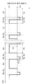
도 1은 하나의 예시적 실시형태에 관한 플라즈마 처리 장치를 개략적으로 도시하는 도면이다.
도 2는 하나의 예시적 실시형태에 관한 플라즈마 처리 방법을 도시하는 흐름도이다.
도 3은 도 2에 도시하는 플라즈마 처리 방법에서의 전원 유닛의 출력 전압의 일례의 타이밍차트이다. 1 is a diagram schematically showing a plasma processing apparatus according to one exemplary embodiment.
Fig. 2 is a flow chart showing a plasma processing method according to an exemplary embodiment.
3 is a timing chart of an example of the output voltage of the power supply unit in the plasma processing method shown in FIG. 2.
이하, 여러가지 예시적 실시형태에 관해 설명한다. Hereinafter, various exemplary embodiments will be described.
하나의 예시적 실시형태에 있어서, 플라즈마 처리 장치가 제공된다. 플라즈마 처리 장치는, 챔버, 기판 지지대, 고주파 전원 및 전원 유닛을 구비한다. 기판 지지대는, 하부 전극을 가지며, 챔버 내에 설치되어 있다. 고주파 전원은, 챔버 내에서 가스로부터 플라즈마를 생성하기 위해 고주파 전력을 공급하도록 구성되어 있다. 전원 유닛은, 정극성의 직류 전압 및 부극성의 직류 전압을 발생시키도록 구성되어 있다. 전원 유닛은, 하부 전극에 전기적으로 접속되어 있다. 전원 유닛은, 챔버 내에서의 에칭 가스로부터의 플라즈마의 생성중인 제1 기간에 있어서, 직류 전압의 하부 전극에 대한 인가를 정지한다. 전원 유닛은, 챔버 내에서의 에칭 가스로부터의 플라즈마의 생성중이자 제1 기간의 이후인 제2 기간에 있어서, 제1 직류 전압을 하부 전극에 인가한다. 제1 직류 전압은 정극성의 직류 전압이다. 전원 유닛은, 기판 지지대 위에 배치된 기판에 대한 에칭을 위해, 챔버 내에서의 에칭 가스로부터의 플라즈마의 생성중이자 제2 기간의 이후인 제3 기간에 있어서, 제2 직류 전압을 하부 전극에 인가한다. 제2 직류 전압은 부극성의 직류 전압이다. 전원 유닛이 출력하는 직류 전압이, 제2 기간에서의 제1 직류 전압으로부터 제3 기간에서의 제2 직류 전압으로 연속적으로 전환된다. In one exemplary embodiment, a plasma processing apparatus is provided. The plasma processing apparatus includes a chamber, a substrate support, a high frequency power supply, and a power supply unit. The substrate support has a lower electrode and is provided in the chamber. The high frequency power supply is configured to supply high frequency power to generate plasma from gas in the chamber. The power supply unit is configured to generate a DC voltage of positive polarity and a DC voltage of negative polarity. The power supply unit is electrically connected to the lower electrode. The power supply unit stops the application of the direct current voltage to the lower electrode in the first period of generation of plasma from the etching gas in the chamber. The power supply unit applies a first direct-current voltage to the lower electrode in the second period during the generation of the plasma from the etching gas in the chamber and after the first period. The first DC voltage is a positive DC voltage. The power supply unit applies a second direct current voltage to the lower electrode in the third period, during the generation of the plasma from the etching gas in the chamber and after the second period, for etching the substrate disposed on the substrate support. do. The second DC voltage is a negative polarity DC voltage. The DC voltage output from the power supply unit is continuously switched from the first DC voltage in the second period to the second DC voltage in the third period.
플라즈마의 생성중에 정극성의 직류 전압이 하부 전극에 인가되면, 플라즈마로부터 음이온 및/또는 전자가 기판에 공급된다. 그 결과, 상기 실시형태에 의하면, 기판의 정전하량이 제2 기간에 있어서 감소된다. 플라즈마의 생성중에 부극성의 직류 전압이 하부 전극에 인가되면, 플라즈마로부터의 플러스 이온이 기판을 향해 가속된다. 그 결과, 상기 실시형태에 의하면, 제3 기간에 있어서 기판이 높은 에칭 레이트로 에칭된다. 또한, 전원 유닛이 출력하는 직류 전압이 제2 기간에서의 제1 직류 전압으로부터 제3 기간에서의 제2 직류 전압으로 연속적으로 전환되기 때문에, 제3 기간에 있어서 기판에 충돌하는 플러스 이온의 에너지가 더욱 향상된다. 따라서, 상기 실시형태에 의하면 에칭 레이트가 더욱 향상된다. When a direct current voltage of positive polarity is applied to the lower electrode during plasma generation, negative ions and / or electrons are supplied from the plasma to the substrate. As a result, according to the above embodiment, the amount of static charge on the substrate is reduced in the second period. When a direct current voltage of negative polarity is applied to the lower electrode during plasma generation, positive ions from the plasma are accelerated toward the substrate. As a result, according to the above embodiment, in the third period, the substrate is etched at a high etching rate. In addition, since the DC voltage output from the power supply unit is continuously switched from the first DC voltage in the second period to the second DC voltage in the third period, the energy of the positive ions impinging on the substrate in the third period is It is further improved. Therefore, according to the above embodiment, the etching rate is further improved.
하나의 예시적 실시형태에 있어서, 제1 직류 전압의 절대치는 제2 직류 전압의 절대치보다 작다. In one exemplary embodiment, the absolute value of the first DC voltage is less than the absolute value of the second DC voltage.
하나의 예시적 실시형태에 있어서, 제3 기간의 시간 길이는, 제1 기간의 시간 길이와 제2 기간의 시간 길이의 합 이하이다. In one exemplary embodiment, the time length of the third period is equal to or less than the sum of the time length of the first period and the time length of the second period.
하나의 예시적 실시형태에 있어서, 제3 기간의 시간 길이는 10 μ초 이하이어도 좋다. In one exemplary embodiment, the time length of the third period may be 10 μsec or less.
하나의 예시적 실시형태에 있어서, 제2 기간의 시간 길이는 제1 기간의 시간 길이 이하이어도 좋다.In one exemplary embodiment, the time length of the second period may be equal to or less than the time length of the first period.
하나의 예시적 실시형태에 있어서, 전원 유닛은, 제1 기간에서의 하부 전극에 대한 직류 전압의 인가의 정지, 제2 기간에서의 하부 전극에 대한 제1 직류 전압의 인가, 및 제3 기간에서의 하부 전극에 대한 제2 직류 전압의 인가를 반복해도 좋다. In one exemplary embodiment, the power supply unit stops the application of the DC voltage to the lower electrode in the first period, the application of the first DC voltage to the lower electrode in the second period, and the third period. The application of the second DC voltage to the lower electrode may be repeated.
하나의 예시적 실시형태에 있어서, 전원 유닛은, 챔버 내에서의 클리닝 가스로부터의 플라즈마의 생성중인 제4 기간에 있어서, 제3 직류 전압을 하부 전극에 인가한다. 제3 직류 전압은 부극성의 직류 전압이다. 전원 유닛은, 챔버 내에서의 클리닝 가스로부터의 플라즈마의 생성중이자 제4 기간의 이후인 제5 기간에 있어서, 직류 전압의 하부 전극에 대한 인가를 추가로 정지한다. 전원 유닛은, 챔버 내에서의 클리닝 가스로부터의 플라즈마의 생성중이자 제5 기간의 이후인 제6 기간에 있어서, 제4 직류 전압을 하부 전극에 인가한다. 제4 직류 전압은 정극성의 직류 전압이다. 제4 기간의 시간 길이는, 제5 기간의 시간 길이와 제6 기간의 시간 길이의 합보다 길다. 제4 기간의 시간 길이가 비교적 긴 경우에는, 제6 기간에 있어서 플라즈마의 전위가 높아진다. 제6 기간에 있어서는 하부 전극에 정극성의 직류 전압이 인가되고 있기 때문에, 플라즈마로부터 챔버의 내벽면을 향해 이온이 가속된다. 그 결과, 챔버의 내벽면에 부착되어 있는 퇴적물이 제거된다. In one exemplary embodiment, the power supply unit applies a third direct current voltage to the lower electrode in the fourth period of plasma generation from the cleaning gas in the chamber. The third DC voltage is a negative polarity DC voltage. The power supply unit further stops the application of the direct voltage to the lower electrode in the fifth period, which is during the generation of the plasma from the cleaning gas in the chamber and after the fourth period. The power supply unit applies the fourth direct current voltage to the lower electrode in the sixth period during the generation of the plasma from the cleaning gas in the chamber and after the fifth period. The fourth DC voltage is a positive DC voltage. The time length of the fourth period is longer than the sum of the time length of the fifth period and the time length of the sixth period. When the time length of the fourth period is relatively long, the potential of the plasma increases in the sixth period. In the sixth period, since a direct voltage of positive polarity is applied to the lower electrode, ions are accelerated from the plasma toward the inner wall surface of the chamber. As a result, sediment adhering to the inner wall surface of the chamber is removed.
하나의 예시적 실시형태에 있어서, 제4 기간의 시간 길이는 제3 기간의 시간 길이보다 길어도 좋다. In one exemplary embodiment, the time length of the fourth period may be longer than the time length of the third period.
하나의 예시적 실시형태에 있어서, 전원 유닛은, 제4 기간에서의 하부 전극에 대한 제3 직류 전압의 인가, 제5 기간에서의 하부 전극에 대한 직류 전압의 인가의 정지, 및 제6 기간에서의 하부 전극에 대한 제4 직류 전압의 인가를 반복해도 좋다. In one exemplary embodiment, the power supply unit is configured to stop the application of the third DC voltage to the lower electrode in the fourth period, the suspension of the application of the DC voltage to the lower electrode in the fifth period, and the sixth period. The application of the fourth DC voltage to the lower electrode may be repeated.
다른 예시적 실시형태에 있어서, 플라즈마 처리 장치를 이용하여 실행되는 플라즈마 처리 방법이 제공된다. 플라즈마 처리 장치는, 챔버, 기판 지지대, 고주파 전원 및 전원 유닛을 구비한다. 기판 지지대는, 하부 전극을 가지며, 챔버 내에 설치되어 있다. 고주파 전원은, 챔버 내에서 가스로부터 플라즈마를 생성하기 위해 고주파 전력을 공급하도록 구성되어 있다. 전원 유닛은, 정극성의 직류 전압 및 부극성의 직류 전압을 발생시키도록 구성되어 있고, 하부 전극에 전기적으로 접속되어 있다. 플라즈마 처리 방법은, 챔버 내에서의 에칭 가스로부터의 플라즈마의 생성중인 제1 기간에 있어서, 전원 유닛으로부터의 직류 전압의 하부 전극에 대한 인가를 정지하는 공정을 포함한다. 플라즈마 처리 방법은, 챔버 내에서의 에칭 가스로부터의 플라즈마의 생성중이자 제1 기간의 이후인 제2 기간에 있어서, 전원 유닛으로부터 하부 전극에 제1 직류 전압을 인가하는 공정을 더 포함한다. 제1 직류 전압은 정극성의 전압이다. 플라즈마 처리 방법은, 기판 지지대 위에 배치된 기판에 대한 에칭을 위해, 챔버 내에서의 에칭 가스로부터의 플라즈마의 생성중이자 제2 기간의 이후인 제3 기간에 있어서, 전원 유닛으로부터 하부 전극에 제2 직류 전압을 인가하는 공정을 더 포함한다. 제2 직류 전압은 부극성의 직류 전압이다. 전원 유닛이 출력하는 직류 전압이, 제2 기간에서의 제1 직류 전압으로부터 제3 기간에서의 제2 직류 전압으로 연속적으로 전환된다. In another exemplary embodiment, a plasma processing method performed using a plasma processing apparatus is provided. The plasma processing apparatus includes a chamber, a substrate support, a high frequency power supply, and a power supply unit. The substrate support has a lower electrode and is provided in the chamber. The high frequency power supply is configured to supply high frequency power to generate plasma from gas in the chamber. The power supply unit is configured to generate a DC voltage of positive polarity and a DC voltage of negative polarity, and is electrically connected to the lower electrode. The plasma processing method includes a step of stopping the application of the DC voltage from the power supply unit to the lower electrode in the first period of plasma generation from the etching gas in the chamber. The plasma processing method further includes a step of applying a first direct current voltage from the power supply unit to the lower electrode in the second period during the generation of the plasma from the etching gas in the chamber and after the first period. The first DC voltage is a positive voltage. The plasma processing method is a second period from the power supply unit to the lower electrode in the third period, during the generation of the plasma from the etching gas in the chamber and after the second period, for etching the substrate disposed on the substrate support. The method further includes applying a DC voltage. The second DC voltage is a negative polarity DC voltage. The DC voltage output from the power supply unit is continuously switched from the first DC voltage in the second period to the second DC voltage in the third period.
하나의 예시적 실시형태에 있어서, 제1 직류 전압의 절대치는 제2 직류 전압의 절대치보다 작다. In one exemplary embodiment, the absolute value of the first DC voltage is less than the absolute value of the second DC voltage.
하나의 예시적 실시형태에 있어서, 제3 기간의 시간 길이는, 제1 기간의 시간 길이와 제2 기간의 시간 길이의 합 이하이다. In one exemplary embodiment, the time length of the third period is equal to or less than the sum of the time length of the first period and the time length of the second period.
하나의 예시적 실시형태에 있어서, 제3 기간의 시간 길이는 10 μ초 이하이어도 좋다.In one exemplary embodiment, the time length of the third period may be 10 μsec or less.
하나의 예시적 실시형태에 있어서, 제2 기간의 시간 길이는 제1 기간의 시간 길이 이하이어도 좋다. In one exemplary embodiment, the time length of the second period may be equal to or less than the time length of the first period.
하나의 예시적 실시형태에 있어서, 정지하는 공정, 제1 직류 전압을 인가하는 공정 및 제2 직류 전압을 인가하는 공정이 반복되어도 좋다. In one exemplary embodiment, the step of stopping, the step of applying the first DC voltage, and the step of applying the second DC voltage may be repeated.
하나의 예시적 실시형태에 있어서, 플라즈마 처리 방법은, 챔버 내에서의 클리닝 가스로부터의 플라즈마의 생성중인 제4 기간에 있어서, 전원 유닛으로부터 하부 전극에 제3 직류 전압을 인가하는 공정을 더 포함한다. 제3 직류 전압은 부극성의 직류 전압이다. 플라즈마 처리 방법은, 챔버 내에서의 클리닝 가스로부터의 플라즈마의 생성중이자 제4 기간의 이후인 제5 기간에 있어서, 전원 유닛으로부터의 직류 전압의 하부 전극에 대한 인가를 추가로 정지하는 공정을 더 포함한다. 플라즈마 처리 방법은, 챔버 내에서의 클리닝 가스로부터의 플라즈마의 생성중이자 제5 기간의 이후인 제6 기간에 있어서, 전원 유닛으로부터 하부 전극에 제4 직류 전압을 인가하는 공정을 더 포함한다. 제4 직류 전압은 정극성의 직류 전압이다. 제4 기간의 시간 길이는, 제5 기간의 시간 길이와 제6 기간의 시간 길이의 합보다 길다. In one exemplary embodiment, the plasma processing method further includes applying a third DC voltage from the power supply unit to the lower electrode in the fourth period of plasma generation from the cleaning gas in the chamber. . The third DC voltage is a negative polarity DC voltage. The plasma treatment method further includes the step of further stopping the application of the direct current voltage from the power supply unit to the lower electrode in the fifth period during the generation of the plasma from the cleaning gas in the chamber and after the fourth period. Includes. The plasma processing method further includes a step of applying a fourth direct current voltage from the power supply unit to the lower electrode in the sixth period during the generation of the plasma from the cleaning gas in the chamber and subsequent to the fifth period. The fourth DC voltage is a positive DC voltage. The time length of the fourth period is longer than the sum of the time length of the fifth period and the time length of the sixth period.
하나의 예시적 실시형태에 있어서, 제4 기간의 시간 길이는 제3 기간의 시간 길이보다 길어도 좋다. In one exemplary embodiment, the time length of the fourth period may be longer than the time length of the third period.
하나의 예시적 실시형태에 있어서, 제3 직류 전압을 인가하는 공정, 추가로 정지하는 공정 및 제4 직류 전압을 인가하는 공정이 반복되어도 좋다. In one exemplary embodiment, the process of applying the third DC voltage, the process of stopping further, and the process of applying the fourth DC voltage may be repeated.
이하, 도면을 참조하여 여러가지 예시적 실시형태에 관해 상세히 설명한다. 또, 각 도면에서 동일 또는 상당 부분에 대해서는 동일한 부호를 붙이기로 한다.Hereinafter, various exemplary embodiments will be described in detail with reference to the drawings. In addition, the same code | symbol is attached | subjected to the same or equivalent part in each figure.
도 1은, 하나의 예시적 실시형태에 관한 플라즈마 처리 장치를 개략적으로 도시하는 도면이다. 도 1에 도시하는 플라즈마 처리 장치(1)는 용량 결합형의 플라즈마 처리 장치이다. 플라즈마 처리 장치(1)는 챔버(10)를 구비하고 있다. 챔버(10)는, 그 안에 내부 공간(10s)을 제공하고 있다. 일 실시형태에 있어서, 챔버(10)는 챔버 본체(12)를 포함하고 있다. 챔버 본체(12)는 대략 원통형상을 갖고 있다. 내부 공간(10s)은 챔버 본체(12) 내에 제공되어 있다. 챔버 본체(12)는, 예컨대 알루미늄으로 구성되어 있다. 챔버 본체(12)는 전기적으로 접지되어 있다. 챔버 본체(12)의 내벽면, 즉, 내부 공간(10s)을 구획하는 벽면에는, 내플라즈마성을 갖는 막이 형성되어 있다. 이 막은, 양극 산화 처리에 의해 형성된 막 또는 산화이트륨으로 형성된 막과 같은 세라믹제의 막일 수 있다. 1 is a diagram schematically showing a plasma processing apparatus according to one exemplary embodiment. The
챔버 본체(12)의 측벽에는 통로(12p)가 형성되어 있다. 기판(W)은, 내부 공간(10s)과 챔버(10)의 외부의 사이에서 반송될 때에 통로(12p)를 통과한다. 이 통로(12p)의 개폐를 위해, 게이트 밸브(12g)가 챔버 본체(12)의 측벽을 따라 설치되어 있다. A
챔버(10) 내에는, 기판 지지대, 즉 지지대(16)가 설치되어 있다. 지지대(16)는, 그 위에 배치된 기판(W)을 지지하도록 구성되어 있다. 기판(W)은, 대략 원반형상을 갖는다. 지지대(16)는 지지체(15)에 의해 지지되어 있다. 지지체(15)는, 챔버 본체(12)의 바닥부로부터 상측으로 연장되어 있다. 지지체(15)는, 대략 원통형상을 갖고 있다. 지지체(15)는, 석영과 같은 절연 재료로 형성되어 있다. In the
지지대(16)는 하부 전극(18)을 갖는다. 지지대(16)는 정전척(20)을 더 가질 수 있다. 지지대(16)는 전극 플레이트(19)를 더 갖고 있어도 좋다. 전극 플레이트(19)는, 알루미늄과 같은 도전성 재료로 형성되어 있고, 대략 원반형상을 갖고 있다. 하부 전극(18)은 전극 플레이트(19) 위에 설치되어 있다. 하부 전극(18)은, 알루미늄과 같은 도전성 재료로 형성되어 있고, 대략 원반형상을 갖고 있다. 하부 전극(18)은 전극 플레이트(19)에 전기적으로 접속되어 있다. The
하부 전극(18) 내에는 유로(18f)가 형성되어 있다. 유로(18f)는 열교환 매체용의 유로이다. 열교환 매체로는, 액상의 냉매, 또는, 그 기화에 의해 하부 전극(18)을 냉각시키는 냉매(예컨대 프론)가 이용된다. 유로(18f)에는 열교환 매체의 순환 장치(예컨대 칠러 유닛)가 접속되어 있다. 이 순환 장치는 챔버(10)의 외부에 설치되어 있다. 유로(18f)에는, 순환 장치로부터 배관(23a)을 통해 열교환 매체가 공급된다. 유로(18f)에 공급된 열교환 매체는, 배관(23b)을 통해 순환 장치로 복귀된다. A
정전척(20)은 하부 전극(18) 위에 설치되어 있다. 기판(W)은, 내부 공간(10s) 내에서 처리될 때에는, 정전척(20) 위에 배치되어, 정전척(20)에 의해 유지된다. 정전척(20)은 본체 및 전극을 갖고 있다. 정전척(20)의 본체는, 산화알루미늄 또는 질화알루미늄과 같은 유전체로 형성되어 있다. 정전척(20)의 본체는 대략 원반형상을 갖고 있다. 정전척(20)은, 기판 배치 영역 및 포커스링 탑재 영역을 포함하고 있다. 기판 배치 영역은 대략 원반형상을 갖는 영역이다. 기판 배치 영역의 상면은 수평면을 따라 연장되어 있다. 기판 배치 영역의 중심을 포함하며, 수직 방향으로 연장되는 축선(AX)은, 챔버(10)의 중심축선과 대략 일치한다. 기판(W)은, 챔버(10) 내에서 처리될 때에는, 기판 배치 영역의 상면 위에 배치된다. The
포커스링 탑재 영역은, 기판 배치 영역을 둘러싸도록 둘레 방향으로 연장되어 있다. 포커스링 탑재 영역의 상면 위에는 포커스링(FR)이 탑재된다. 포커스링(FR)은 고리 형상을 갖고 있다. 기판(W)은 포커스링(FR)에 의해 둘러싸인 영역 내에 배치된다. 즉, 포커스링(FR)은, 정전척(20)의 기판 배치 영역 위에 배치된 기판(W)의 엣지를 둘러싼다. 포커스링(FR)은, 예컨대 실리콘 또는 탄화규소로 형성되어 있다. The focus ring mounting region extends in the circumferential direction so as to surround the substrate placement region. The focus ring FR is mounted on the top surface of the focus ring mounting area. The focus ring FR has a ring shape. The substrate W is disposed in an area surrounded by the focus ring FR. That is, the focus ring FR surrounds the edge of the substrate W disposed on the substrate placement region of the
정전척(20)의 전극은 정전척(20)의 본체 내에 설치되어 있다. 정전척(20)의 전극은 도체로 형성된 막이다. 정전척(20)의 전극에는 직류 전원이 전기적으로 접속되어 있다. 직류 전원으로부터 정전척(20)의 전극에 직류 전압이 인가되면, 정전척(20)과 기판(W)의 사이에서 정전인력이 발생한다. 발생한 정전인력에 의해, 기판(W)은 정전척(20)으로 끌어당겨져, 정전척(20)에 의해 유지된다. The electrode of the
플라즈마 처리 장치(1)는, 가스 공급 라인(25)을 더 구비할 수 있다. 가스 공급 라인(25)은, 가스 공급 기구로부터의 전열 가스, 예컨대 He 가스를, 정전척(20)의 상면과 기판(W)의 이면(하면) 사이에 공급한다. The
플라즈마 처리 장치(1)는, 통형부(28) 및 절연부(29)를 더 구비할 수 있다. 통형부(28)는, 챔버 본체(12)의 바닥부로부터 상측으로 연장되어 있다. 통형부(28)는 지지체(15)의 외주를 따라 연장되어 있다. 통형부(28)는, 도전성 재료로 형성되어 있고, 대략 원통형상을 갖고 있다. 통형부(28)는 전기적으로 접지되어 있다. 절연부(29)는 통형부(28) 위에 설치되어 있다. 절연부(29)는 절연성을 갖는 재료로 형성되어 있다. 절연부(29)는, 예컨대 석영과 같은 세라믹으로 형성되어 있다. 절연부(29)는 대략 원통형상을 갖고 있다. 절연부(29)는, 전극 플레이트(19)의 외주, 하부 전극(18)의 외주 및 정전척(20)의 외주를 따라 연장되어 있다. The
플라즈마 처리 장치(1)는 상부 전극(30)을 더 구비하고 있다. 상부 전극(30)은 지지대(16)의 상측에 설치되어 있다. 상부 전극(30)은, 부재(32)와 함께 챔버 본체(12)의 상부 개구를 폐쇄하고 있다. 부재(32)는 절연성을 갖고 있다. 상부 전극(30)은, 이 부재(32)를 통해 챔버 본체(12)의 상부에 지지되어 있다. The
상부 전극(30)은, 상판(34) 및 지지체(36)를 포함하고 있다. 상판(34)의 하면은 내부 공간(10s)을 구획하고 있다. 상판(34)에는 복수의 가스 토출 구멍(34a)이 형성되어 있다. 복수의 가스 토출 구멍(34a)의 각각은, 상판(34)을 판두께 방향(수직 방향)으로 관통하고 있다. 이 상판(34)은, 한정되는 것은 아니지만, 예컨대 실리콘으로 형성되어 있다. 또는, 상판(34)은, 알루미늄제 부재의 표면에 내플라즈마성의 막을 설치한 구조를 가질 수 있다. 이 막은, 양극 산화 처리에 의해 형성된 막 또는 산화이트륨으로 형성된 막과 같은 세라믹제의 막일 수 있다. The
지지체(36)는, 상판(34)을 착탈 가능하게 지지하고 있다. 지지체(36)는, 예컨대 알루미늄과 같은 도전성 재료로 형성되어 있다. 지지체(36)의 내부에는 가스 확산실(36a)이 설치되어 있다. 가스 확산실(36a)로부터는 복수의 가스 구멍(36b)이 하측으로 연장되고 있다. 복수의 가스 구멍(36b)은 복수의 가스 토출 구멍(34a)에 각각 연통하고 있다. 지지체(36)에는 가스 도입 포트(36c)가 형성되어 있다. 가스 도입 포트(36c)는 가스 확산실(36a)에 접속하고 있다. 가스 도입 포트(36c)에는 가스 공급관(38)이 접속되어 있다. The
가스 공급관(38)에는, 가스 소스군(40)이, 밸브군(41), 유량 제어기군(42) 및 밸브군(43)을 통해 접속되어 있다. 가스 소스군(40), 밸브군(41), 유량 제어기군(42) 및 밸브군(43)은 가스 공급부를 구성하고 있다. 가스 소스군(40)은 복수의 가스 소스를 포함하고 있다. 복수의 가스 소스는, 여러가지 실시형태에 관한 플라즈마 처리 방법에서 이용되는 복수의 가스의 소스를 포함하고 있다. 복수의 가스는 에칭 가스 및 클리닝 가스를 포함하고 있다. 밸브군(41) 및 밸브군(43)의 각각은, 복수의 밸브(예컨대 개폐 밸브)를 포함하고 있다. 유량 제어기군(42)은 복수의 유량 제어기를 포함하고 있다. 유량 제어기군(42)의 복수의 유량 제어기의 각각은, 매스플로우 컨트롤러 또는 압력 제어식의 유량 제어기이다. 가스 소스군(40)의 복수의 가스 소스의 각각은, 밸브군(41)에 대응하는 밸브, 유량 제어기군(42)에 대응하는 유량 제어기, 및 밸브군(43)에 대응하는 밸브를 통해, 가스 공급관(38)에 접속되어 있다. 플라즈마 처리 장치(1)는, 가스 소스군(40)의 복수의 가스 소스 중 선택된 1 이상의 가스 소스로부터의 가스를, 개별로 조정된 유량으로 내부 공간(10s)에 공급하는 것이 가능하다. The
통형부(28)와 챔버 본체(12)의 측벽 사이에는 배플 부재(48)가 설치되어 있다. 배플 부재(48)는 판형의 부재일 수 있다. 배플 부재(48)는, 예컨대 알루미늄제의 판재에 산화이트륨 등의 세라믹을 피복하는 것에 의해 구성될 수 있다. 이 배플 부재(48)에는 복수의 관통 구멍이 형성되어 있다. 배플 부재(48)의 하측에 있어서는, 배기관(52)이 챔버 본체(12)의 바닥부에 접속되어 있다. 이 배기관(52)에는 배기 장치(50)가 접속되어 있다. 배기 장치(50)는, 자동 압력 제어 밸브와 같은 압력 제어기, 및, 터보 분자 펌프 등의 진공 펌프를 갖고 있어, 내부 공간(10s) 내의 압력을 감압할 수 있다. A
플라즈마 처리 장치(1)는 고주파 전원(61)을 더 구비한다. 고주파 전원(61)은, 플라즈마 생성용의 고주파 전력을 발생시키는 전원이다. 고주파 전력의 주파수는, 한정되는 것은 아니지만, 27∼100 MHz의 범위 내의 주파수, 예컨대 40 MHz 또는 60 MHz이다. 고주파 전원(61)은, 고주파 전력을 하부 전극(18)에 공급하기 위해, 정합기(63) 및 전극 플레이트(19)를 통해 하부 전극(18)에 접속되어 있다. 정합기(63)는, 고주파 전원(61)의 출력 임피던스와 부하측(하부 전극(18)측)의 임피던스를 정합시키기 위한 정합 회로를 갖고 있다. 또, 고주파 전원(61)은, 하부 전극(18)에 전기적으로 접속되어 있지 않아도 좋고, 정합기(63)를 통해 상부 전극(30)에 접속되어 있어도 좋다. The
플라즈마 처리 장치(1)는 전원 유닛(64)을 더 구비한다. 전원 유닛(64)은, 하부 전극(18)에 인가되는 직류 전압을 발생시키도록 구성되어 있다. 전원 유닛(64)은, 부극성의 직류 전압 및 정극성의 직류 전압을 발생시키도록 구성되어 있다. 전원 유닛(64)은 하부 전극(18)에 전기적으로 접속되어 있다. 일 실시형태에서는, 전원 유닛(64)은, 로우패스 필터(66)를 통해 정합기(63)와 전극 플레이트(19)를 서로 접속하는 전기적 패스에 접속되어 있다. 전원 유닛(64)의 동작의 상세에 관해서는 후술한다. The
플라즈마 처리 장치(1)에서는 내부 공간(10s)에 가스가 공급된다. 그리고, 고주파 전력이 공급되는 것에 의해, 내부 공간(10s) 중에서 가스가 여기된다. 그 결과, 내부 공간(10s) 중에서 플라즈마가 생성된다. 생성된 플라즈마로부터의 이온 및/또는 라디칼과 같은 화학종에 의해 기판(W)이 처리된다. 또는, 생성된 플라즈마로부터의 이온 및/또는 라디칼과 같은 화학종에 의해, 챔버(10)의 내벽면의 클리닝이 행해진다. In the
플라즈마 처리 장치(1)는 제어부(MC)를 더 구비한다. 제어부(MC)는, 프로세서, 기억 장치, 입력 장치, 표시 장치 등을 구비하는 컴퓨터이며, 플라즈마 처리 장치(1)의 각 부를 제어한다. 구체적으로, 제어부(MC)는 기억 장치에 기억되어 있는 제어 프로그램을 실행하고, 상기 기억 장치에 기억되어 있는 레시피 데이터에 기초하여 플라즈마 처리 장치(1)의 각 부를 제어한다. 제어부(MC)에 의한 제어에 의해, 레시피 데이터에 의해 지정된 프로세스가 플라즈마 처리 장치(1)에 있어서 실행된다. 여러가지 실시형태에 관한 플라즈마 처리 방법은, 제어부(MC)에 의한 플라즈마 처리 장치(1)의 각 부의 제어에 의해, 플라즈마 처리 장치(1)에 있어서 실행될 수 있다. The
이하, 도 2 및 도 3을 참조하여, 하나의 예시적 실시형태에 관한 플라즈마 처리 방법에 관해 설명한다. 도 2는, 하나의 예시적 실시형태에 관한 플라즈마 처리 방법을 도시하는 흐름도이다. 도 3은, 도 2에 도시하는 플라즈마 처리 방법에서의 전원 유닛의 출력 전압의 일례의 타이밍차트이다. 이하에서는, 도 2에 도시하는 플라즈마 처리 방법(이하, 「방법 MT」이라고 함)에서의 플라즈마 처리 장치(1)의 각 부의 동작에 관해서도 설명한다. Hereinafter, a plasma processing method according to one exemplary embodiment will be described with reference to FIGS. 2 and 3. Fig. 2 is a flow chart showing a plasma processing method according to one exemplary embodiment. 3 is a timing chart of an example of the output voltage of the power supply unit in the plasma processing method shown in FIG. 2. Hereinafter, the operation of each part of the
도 2에 도시한 바와 같이, 방법 MT의 공정 STa에서는, 에칭 가스로부터의 플라즈마의 생성이 시작된다. 에칭 가스는, 기판(W)의 플라즈마 에칭을 위해 이용되는 가스이다. 공정 STa에 있어서, 제어부(MC)는, 챔버(10) 내에 에칭 가스를 공급하도록 가스 공급부를 제어한다. 공정 STa에 있어서, 제어부(MC)는, 챔버(10) 내의 압력을 지정된 압력으로 설정하도록 배기 장치(50)를 제어한다. 공정 STa에 있어서, 제어부(MC)는, 고주파 전력을 하부 전극(18)(또는 상부 전극(30))에 공급하도록 고주파 전원(61)을 제어한다. As shown in Fig. 2, in the process STa of the method MT, plasma generation from the etching gas is started. The etching gas is a gas used for plasma etching of the substrate W. In step STa, the control unit MC controls the gas supply unit to supply the etching gas into the
방법 MT은, 공정 ST1, 공정 ST2 및 공정 ST3을 포함한다. 공정 ST1, 공정 ST2 및 공정 ST3은, 공정 STa에서 시작된 에칭 가스로부터의 플라즈마의 생성중에 실행된다. 공정 ST1의 실행 기간은 제1 기간 P1이다. 공정 ST2의 실행 기간은 제2 기간 P2이다. 공정 ST3의 실행 기간은 제3 기간 P3이다. 에칭 가스로부터 플라즈마를 생성하기 위해, 고주파 전력은, 제1 기간 P1, 제2 기간 P2 및 제3 기간 P3에 걸쳐 연속적으로 공급되어도 좋다. The method MT includes Step ST1, Step ST2, and Step ST3. Step ST1, step ST2, and step ST3 are performed during the generation of plasma from the etching gas started in step STa. The execution period of step ST1 is the first period P1. The execution period of step ST2 is the second period P2. The execution period of step ST3 is the third period P3. In order to generate plasma from the etching gas, high-frequency power may be continuously supplied over the first period P1, the second period P2, and the third period P3.
공정 ST1은 제1 기간 P1에 있어서 실행된다. 제1 기간 P1은, 챔버(10) 내에서의 에칭 가스로부터의 플라즈마의 생성중의 기간이다. 공정 ST1은, 제1 기간 P1에 있어서 전원 유닛(64)으로부터의 직류 전압의 하부 전극(18)에 대한 인가를 정지하는 것을 포함한다. 공정 ST1의 실행을 위해, 제어부(MC)는, 제1 기간 P1에 있어서 직류 전압의 하부 전극(18)에 대한 출력을 정지하도록 전원 유닛(64)을 제어한다. Step ST1 is executed in the first period P1. The first period P1 is a period during plasma generation from the etching gas in the
공정 ST2는 제2 기간 P2에 있어서 실행된다. 제2 기간 P2은, 챔버(10) 내에서의 에칭 가스로부터의 플라즈마의 생성중의 기간이며, 제1 기간 P1 이후의 기간이다. 공정 ST2는, 제2 기간 P2에 있어서 전원 유닛(64)으로부터 하부 전극(18)에 제1 직류 전압(V1)을 인가하는 것을 포함한다. 제1 직류 전압(V1)은 정극성의 직류 전압이다. 공정 ST2의 실행을 위해, 제어부(MC)는, 제2 기간 P2에 있어서 하부 전극(18)에 제1 직류 전압(V1)을 인가하도록 전원 유닛(64)을 제어한다. Step ST2 is executed in the second period P2. The second period P2 is a period during plasma generation from the etching gas in the
공정 ST3은 제3 기간 P3에 있어서 실행된다. 제3 기간 P3은, 챔버(10) 내에서의 에칭 가스로부터의 플라즈마의 생성중의 기간이며, 제2 기간 P2 이후의 기간이다. 공정 ST3은, 제3 기간 P3에 있어서 전원 유닛(64)으로부터 하부 전극(18)에 제2 직류 전압(V2)을 인가하는 것을 포함한다. 제2 직류 전압(V2)은 부극성의 직류 전압이다. 일 실시형태에서는, 도 3에 도시한 바와 같이, 제1 직류 전압의 절대치 |V1|는 제2 직류 전압의 절대치 |V2|보다 작다. 제2 직류 전압의 절대치 |V2|는, 기판(W)에 깊은 개구를 형성하는 경우에는 3 kV 이상으로 설정될 수 있다. 제2 직류 전압의 절대치 |V2|는, 게이트 형성을 위한 폴리실리콘의 에칭이 행해지는 경우에는 500 V 이하로 설정될 수 있다. 제2 직류 전압의 절대치 |V2|는, 폴리실리콘의 패터닝을 위한 에칭이 행해지는 경우에는, 5 V 이상, 300 V 이하로 설정될 수 있다. 공정 ST3의 실행을 위해, 제어부(MC)는, 제3 기간 P3에 있어서 하부 전극(18)에 제2 직류 전압(V2)을 인가하도록 전원 유닛(64)을 제어한다. Step ST3 is executed in the third period P3. The third period P3 is a period during plasma generation from the etching gas in the
전원 유닛(64)이 출력하는 직류 전압은, 제2 기간 P2에서의 제1 직류 전압(V1)으로부터 제3 기간 P3에서의 제2 직류 전압(V2)으로 연속적으로 전환된다. 즉, 전원 유닛(64)이 제1 직류 전압(V1)의 출력을 정지하는 제2 기간 P2의 종료 시점과 전원 유닛(64)이 제2 직류 전압(V2)의 출력을 시작하는 제3 기간 P3의 시작 시점은, 서로 동일하거나 연속해 있다. The DC voltage output from the
일 실시형태에서는, 도 3에 도시한 바와 같이, 제3 기간 P3의 시간 길이 T3은, 제1 기간 P1의 시간 길이 T1과 제2 기간 P2의 시간 길이 T2의 합 이하이다. 즉, T3≤T1+T2가 만족된다. 환언하면, 제1 기간 P1, 제2 기간 P2 및 제3 기간 P3으로 이루어진 기간에 있어서 제3 기간 P3이 차지하는 비율(즉 듀티비)은 50% 이하이다. 제3 기간 P3의 시간 길이 T3은, 예컨대 10 μ초 이하이다. 일 실시형태에서는, 도 3에 도시한 바와 같이, 제2 기간 P2의 시간 길이 T2는, 제1 기간 P1의 시간 길이 T1 이하이어도 좋다. In one embodiment, as shown in FIG. 3, the time length T3 of the third period P3 is equal to or less than the time length T1 of the first period P1 and the time length T2 of the second period P2. That is, T3≤T1 + T2 is satisfied. In other words, in the period consisting of the first period P1, the second period P2, and the third period P3, the ratio (that is, the duty ratio) of the third period P3 is 50% or less. The time length T3 of the third period P3 is, for example, 10 μsec or less. In one embodiment, as shown in FIG. 3, the time length T2 of the second period P2 may be equal to or less than the time length T1 of the first period P1.
플라즈마의 생성중에 정극성의 직류 전압이 하부 전극(18)에 인가되면, 플라즈마로부터 음이온 및/또는 전자가 기판(W)에 공급된다. 그 결과, 기판(W)의 정전하량이 제2 기간 P2에 있어서 감소된다. 플라즈마의 생성중에 부극성의 직류 전압이 하부 전극(18)에 인가되면, 플라즈마로부터의 플러스 이온이 기판(W)을 향해 가속된다. 그 결과, 제3 기간 P3에 있어서 기판(W)이 높은 에칭 레이트로 에칭된다. 또한, 전원 유닛(64)이 출력하는 직류 전압이 제2 기간 P2에서의 제1 직류 전압(V1)으로부터 제3 기간 P3에서의 제2 직류 전압(V2)으로 연속적으로 전환되기 때문에, 제3 기간 P3에 있어서 기판에 충돌하는 플러스 이온의 에너지가 더욱 향상된다. 따라서, 에칭 레이트가 더욱 향상된다. When a direct current voltage of positive polarity is applied to the
일 실시형태에 있어서, 공정 ST1, 공정 ST2 및 공정 ST3은, 이 순으로 반복되어도 좋다. 이 경우에는, 도 2에 도시한 바와 같이, 방법 MT은 공정 STb를 더 포함한다. 공정 STb에서는, 정지 조건이 만족되는지 아닌지가 판정된다. 정지 조건은, 공정 ST1, 공정 ST2 및 공정 ST3의 반복 횟수가 소정 횟수에 도달한 경우에 만족된다. 또한, 공정 ST1, 공정 ST2 및 공정 ST3의 반복 주파수, 즉, (T1+T2+T3)의 역수는, 10 kHz 이상 400 kHz 이하이어도 좋다. 또는, 상기 주파수는 400 kHz보다 높아도 좋다. In one embodiment, step ST1, step ST2, and step ST3 may be repeated in this order. In this case, as shown in Fig. 2, the method MT further includes a process STb. In step STb, it is determined whether or not the stop condition is satisfied. The stop condition is satisfied when the number of repetitions of step ST1, step ST2 and step ST3 reaches a predetermined number of times. In addition, the repetition frequency of step ST1, step ST2, and step ST3, that is, the reciprocal of (T1 + T2 + T3) may be 10 kHz or more and 400 kHz or less. Alternatively, the frequency may be higher than 400 kHz.
공정 STb에 있어서 정지 조건이 만족되지 않았다고 판정되면, 다시 공정 ST1이 실행된다. 한편, 공정 STb에 있어서, 정지 조건이 만족되었다고 판정되면, 공정 STc이 실행되어도 좋다. 또, 공정 STa 및 공정 ST1∼공정 ST3의 실행에 의한 플라즈마 에칭이, 복수의 기판에 대하여 순서대로 실행된 후에, 공정 STc이 실행되어도 좋다. If it is determined in step STb that the stop condition is not satisfied, step ST1 is executed again. On the other hand, in step STb, if it is determined that the stop condition is satisfied, step STc may be executed. In addition, after the plasma etching by the execution of steps STa and steps ST1 to ST3 is performed sequentially on a plurality of substrates, step STc may be performed.
공정 STc이 실행되는 경우에는, 지지대(16) 위에 배치되는 물체가 공정 ST1∼공정 ST3에 의해 처리된 기판(W)으로부터 더미 기판으로 교환되어, 상기 더미 기판이 정전척(20)에 의해 유지된다. 이 경우에는, 공정 STc 및 후술하는 공정 ST4∼공정 ST6은, 더미 기판이 지지대(16) 위에 배치된 상태로 실행된다. 또, 공정 STc 및 공정 ST4∼공정 ST6은, 지지대(16) 위에 물체가 배치되지 않은 상태로 실행되어도 좋다. 이 경우에는, 공정 STc의 실행전에 기판(W)이 챔버(10)로부터 반출된다. 또는, 공정 STc 및 공정 ST4∼공정 ST6은, 공정 ST1∼공정 ST3에 의해 처리된 기판(W)이 지지대(16) 위에 배치되어 있는 상태로 실행되어도 좋다. When step STc is executed, the object disposed on the
공정 STc에서는, 클리닝 가스로부터의 플라즈마의 생성이 시작된다. 클리닝 가스는, 챔버(10)의 내벽면에 부착되어 있는 퇴적물을 제거하기 위해 이용되는 가스이다. 공정 STc에 있어서, 제어부(MC)는, 챔버(10) 내에 클리닝 가스를 공급하도록 가스 공급부를 제어한다. 공정 STc에 있어서, 제어부(MC)는, 챔버(10) 내의 압력을 지정된 압력으로 설정하도록 배기 장치(50)를 제어한다. 공정 STc에 있어서, 제어부(MC)는, 고주파 전력을 하부 전극(18)(또는 상부 전극(30))에 공급하도록 고주파 전원(61)을 제어한다. In step STc, plasma generation from the cleaning gas is started. The cleaning gas is a gas used to remove deposits attached to the inner wall surface of the
방법 MT은, 공정 ST4, 공정 ST5 및 공정 ST6을 더 포함하고 있어도 좋다. 공정 ST4, 공정 ST5 및 공정 ST6은, 공정 STc에서 시작된 클리닝 가스로부터의 플라즈마의 생성중에 실행된다. 공정 ST4의 실행 기간은 제4 기간 P4이다. 공정 ST5의 실행 기간은 제5 기간 P5이다. 공정 ST6의 실행 기간은 제6 기간 P6이다. 클리닝 가스로부터 플라즈마를 생성하기 위해, 고주파 전력은 제4 기간 P4, 제5 기간 P5 및 제6 기간 P6에 걸쳐 연속적으로 공급되어도 좋다. The method MT may further include a step ST4, a step ST5, and a step ST6. Step ST4, step ST5, and step ST6 are performed during the generation of plasma from the cleaning gas started in step STc. The execution period of step ST4 is the fourth period P4. The execution period of step ST5 is the fifth period P5. The execution period of step ST6 is the sixth period P6. In order to generate plasma from the cleaning gas, high-frequency power may be continuously supplied over the fourth period P4, the fifth period P5, and the sixth period P6.
공정 ST4는 제4 기간 P4에 있어서 실행된다. 제4 기간 P4는, 챔버(10) 내에서의 클리닝 가스로부터의 플라즈마의 생성중의 기간이다. 공정 ST4는, 제4 기간 P4에 있어서, 전원 유닛(64)으로부터 하부 전극(18)에 제3 직류 전압(V3)을 인가하는 것을 포함한다. 제3 직류 전압(V3)은 부극성의 직류 전압이다. 제어부(MC)는, 제4 기간 P4에 있어서, 제3 직류 전압(V3)을 하부 전극(18)에 인가하도록 전원 유닛(64)을 제어한다. Step ST4 is executed in the fourth period P4. The fourth period P4 is a period during the generation of plasma from the cleaning gas in the
공정 ST5는 제5 기간 P5에 있어서 실행된다. 제5 기간 P5는, 챔버(10) 내에서의 클리닝 가스로부터의 플라즈마의 생성중의 기간이며, 제4 기간 P4 이후의 기간이다. 공정 ST5는, 제5 기간 P5에 있어서 전원 유닛(64)으로부터의 직류 전압의 하부 전극(18)에 대한 인가를 정지하는 것을 포함한다. 공정 ST5의 실행을 위해, 제어부(MC)는, 제5 기간 P5에 있어서 직류 전압의 하부 전극(18)에 대한 출력을 정지하도록 전원 유닛(64)을 제어한다. Step ST5 is executed in the fifth period P5. The fifth period P5 is a period during plasma generation from the cleaning gas in the
공정 ST6은 제6 기간 P6에 있어서 실행된다. 제6 기간 P6은, 챔버(10) 내에서의 클리닝 가스로부터의 플라즈마의 생성중의 기간이며, 제5 기간 P5 이후의 기간이다. 공정 ST6은, 제6 기간 P6에 있어서 전원 유닛(64)으로부터 하부 전극(18)에 제4 직류 전압(V4)을 인가하는 것을 포함한다. 제4 직류 전압(V4)은 정극성의 직류 전압이다. 공정 ST6의 실행을 위해, 제어부(MC)는, 제6 기간 P6에 있어서 하부 전극(18)에 제4 직류 전압(V4)을 인가하도록 전원 유닛(64)을 제어한다. Step ST6 is executed in the sixth period P6. The sixth period P6 is a period during plasma generation from the cleaning gas in the
제6 기간 P6에 있어서는 하부 전극(18)에 제4 직류 전압(V4), 즉 정극성의 직류 전압이 인가되고 있기 때문에, 플라즈마로부터 챔버(10)의 내벽면을 향해 이온이 가속된다. 그 결과, 챔버(10)의 내벽면에 부착되어 있는 퇴적물이 제거된다. In the sixth period P6, since the fourth DC voltage V4, that is, the positive DC voltage, is applied to the
일 실시형태에서는, 도 3에 도시한 바와 같이, 제4 직류 전압의 절대치 |V4|는 제3 직류 전압의 절대치 |V3|보다 작다. 또, 제4 직류 전압(V4)은 제1 직류 전압(V1)과 동일해도 좋다. 제4 직류 전압(V4)은 제로이어도 좋다. 단, 제4 직류 전압의 절대치 |V4|가 큰 경우에는, 플라즈마의 포텐셜이 높아지고, 높은 에너지를 갖는 이온이 챔버(10)의 내벽면을 향해 공급된다. 제3 직류 전압(V3)은 제2 직류 전압(V2)과 동일해도 좋다. 또는, 제3 직류 전압의 절대치 |V3|는, 조건: |V2|>|V3|≥0을 만족하고 있어도 좋다. 이 조건이 만족되는 경우에는, 제3 직류 전압의 절대치 |V3|는 비교적 작다. 따라서, 지지대(16) 위에 물체가 배치되어 있지 않은 상태로 공정 STc 및 후술하는 공정 ST4∼공정 ST6이 실행되는 경우에, 정전척(20)의 손상이 억제된다. In one embodiment, as shown in Fig. 3, the absolute value | V4 | of the fourth DC voltage is smaller than the absolute value | V3 | of the third DC voltage. Further, the fourth DC voltage V4 may be the same as the first DC voltage V1. The fourth DC voltage V4 may be zero. However, when the absolute value | V4 | of the fourth DC voltage is large, the potential of the plasma increases, and ions having high energy are supplied toward the inner wall surface of the
도 3에 도시한 바와 같이, 제4 기간 P4의 시간 길이 T4는, 제5 기간 P5의 시간 길이 T5와 제6 기간 P6의 시간 길이 T6의 합보다 길다. 즉, T4>T5+T6이 만족된다. 환언하면, 제4 기간 P4, 제5 기간 P5 및 제6 기간 P6으로 이루어진 기간에 있어서 제4 기간 P4이 차지하는 비율(즉 듀티비)은 50%보다 크다. 일 실시형태에 있어서, 제4 기간 P4의 시간 길이 T4는 제3 기간 P3의 시간 길이 T3의 시간 길이보다 길다. 즉, 일 실시형태에서는 T4>T3이 만족된다. 제4 기간 P4의 시간 길이 T4가 비교적 긴 경우에는, 제4 직류 전압(V4)이 커지고, 제6 기간 P6에 있어서 플라즈마의 포텐셜이 높아진다. 따라서, 높은 에너지를 갖는 이온이 챔버(10)의 내벽면을 향해 공급되고, 챔버(10)의 내벽면의 클리닝의 효율이 높아진다. 일 실시형태에 있어서, 제6 기간 P6의 시간 길이 T6은 제2 기간 P2의 시간 길이 T2 보다 길다. 즉, 일 실시형태에서는 T2<T6이 만족된다. 이 실시형태에서는, 제4 직류 전압(V4)이 인가되고 있는 기간의 시간 길이가 길어진다. 따라서, 제4 직류 전압(V4)이 직사각형의 전압으로서 인가되고, 챔버(10)의 내벽면의 클리닝의 효과가 충분히 발휘된다. As shown in FIG. 3, the time length T4 of the fourth period P4 is longer than the sum of the time length T5 of the fifth period P5 and the time length T6 of the sixth period P6. That is, T4> T5 + T6 is satisfied. In other words, in the period consisting of the fourth period P4, the fifth period P5, and the sixth period P6, the ratio (that is, the duty ratio) of the fourth period P4 is greater than 50%. In one embodiment, the time length T4 of the fourth period P4 is longer than the time length T3 of the third period P3. That is, in one embodiment, T4> T3 is satisfied. When the time length T4 of the fourth period P4 is relatively long, the fourth DC voltage V4 increases, and the potential of the plasma increases in the sixth period P6. Therefore, ions having high energy are supplied toward the inner wall surface of the
일 실시형태에 있어서, 공정 ST4, 공정 ST5 및 공정 ST6은 이 순으로 반복되어도 좋다. 이 경우에는, 도 2에 도시한 바와 같이, 방법 MT은 공정 STd를 더 포함한다. 공정 STd에서는, 정지 조건이 만족되었는지 아닌지가 판정된다. 정지 조건은, 공정 ST4, 공정 ST5 및 공정 ST6의 반복 횟수가 소정 횟수에 도달한 경우에 만족된다. 또, 공정 ST4, 공정 ST5 및 공정 ST6의 반복의 주파수, 즉 (T4+T5+T6)의 역수는, 10 kHz 이상 400 kHz 이하이어도 좋다. 또는, 상기 주파수는 400 kHz보다 높아도 좋다. 또한, (T4+T5+T6)은 (T1+T2+T3)과 같아도 좋다. In one embodiment, step ST4, step ST5, and step ST6 may be repeated in this order. In this case, as shown in Fig. 2, the method MT further includes a process STd. In step STd, it is determined whether or not the stop condition is satisfied. The stop condition is satisfied when the number of repetitions of steps ST4, ST5, and ST6 reaches a predetermined number of times. In addition, the repetition frequency of step ST4, step ST5, and step ST6, that is, the reciprocal of (T4 + T5 + T6) may be 10 kHz or more and 400 kHz or less. Alternatively, the frequency may be higher than 400 kHz. Further, (T4 + T5 + T6) may be the same as (T1 + T2 + T3).
공정 STd에 있어서 정지 조건이 만족되지 않았다고 판정되면, 다시 공정 ST4가 실행된다. 한편, 공정 STd에 있어서, 정지 조건이 만족되었다고 판정되면, 방법 MT은 종료한다. If it is determined in step STd that the stop condition is not satisfied, step ST4 is executed again. On the other hand, if it is determined in step STd that the stop condition is satisfied, the method MT ends.
이상, 여러가지 예시적 실시형태에 관해 설명했지만, 전술한 예시적 실시형태에 한정되지 않고, 여러가지 생략, 치환 및 변경이 행해져도 좋다. 또한, 상이한 실시형태에서의 요소를 조합하여 다른 실시형태를 형성하는 것이 가능하다. The various exemplary embodiments have been described above, but are not limited to the exemplary embodiments described above, and various omissions, substitutions, and changes may be made. It is also possible to combine elements in different embodiments to form other embodiments.
예컨대, 플라즈마 처리 장치(1)는 용량 결합형의 플라즈마 처리 장치였지만, 별도의 실시형태에 관한 플라즈마 처리 장치는, 유도 결합형의 플라즈마 처리 장치와 같은 다른 타입의 플라즈마 처리 장치이어도 좋다. 또한, 방법 MT은, 플라즈마 처리 장치(1) 이외의 임의의 타입의 플라즈마 처리 장치, 예컨대 유도 결합형의 플라즈마 처리 장치를 이용하여 실행되어도 좋다. For example, the
이상의 설명으로부터, 본 개시의 여러가지 실시형태는, 설명의 목적으로 본 명세서에서 설명되어 있고, 본 개시의 범위 및 주지로부터 일탈하지 않고 여러가지 변경을 할 수 있는 것이 이해될 것이다. 따라서, 본 명세서에 개시한 여러가지 실시형태는 한정하는 것을 의도하지 않으며, 실제 범위와 주지는 첨부한 청구범위에 의해 제시된다. From the above description, it will be understood that various embodiments of the present disclosure are described herein for purposes of explanation, and various changes can be made without departing from the scope and spirit of the present disclosure. Accordingly, various embodiments disclosed herein are not intended to be limiting, and the actual scope and well-known are set forth by the appended claims.
Claims (18)
하부 전극을 가지며, 상기 챔버 내에 설치된 기판 지지대와,
상기 챔버 내에서 가스로부터 플라즈마를 생성하기 위해 고주파 전력을 공급하도록 구성된 고주파 전원과,
정극성의 직류 전압 및 부극성의 직류 전압을 발생시키도록 구성되어 있고, 상기 하부 전극에 전기적으로 접속된 전원 유닛
을 구비하고,
상기 전원 유닛은,
상기 챔버 내에서의 에칭 가스로부터의 플라즈마의 생성중인 제1 기간에 있어서, 직류 전압의 상기 하부 전극에 대한 인가를 정지하고,
상기 챔버 내에서의 상기 에칭 가스로부터의 상기 플라즈마의 생성중이자 상기 제1 기간의 이후인 제2 기간에 있어서, 정극성의 직류 전압인 제1 직류 전압을 상기 하부 전극에 인가하고,
상기 기판 지지대 위에 배치된 기판에 대한 에칭을 위해, 상기 챔버 내에서의 상기 에칭 가스로부터의 상기 플라즈마의 생성중이자 상기 제2 기간의 이후인 제3 기간에 있어서, 부극성의 직류 전압인 제2 직류 전압을 상기 하부 전극에 인가
하도록 구성되어 있고,
상기 전원 유닛이 출력하는 직류 전압이, 상기 제2 기간에서의 상기 제1 직류 전압으로부터 상기 제3 기간에서의 상기 제2 직류 전압으로 연속적으로 전환되는, 플라즈마 처리 장치.Chamber,
A substrate support having a lower electrode and installed in the chamber,
A high frequency power supply configured to supply high frequency power to generate plasma from gas in the chamber;
A power supply unit configured to generate a positive-polarity DC voltage and a negative-polarity DC voltage, and electrically connected to the lower electrode.
Equipped with,
The power unit,
In the first period of plasma generation from the etching gas in the chamber, the application of the DC voltage to the lower electrode is stopped,
In the second period during the generation of the plasma from the etching gas in the chamber and after the first period, a first direct current voltage that is a direct current voltage of positive polarity is applied to the lower electrode,
For the etching of the substrate disposed on the substrate support, in the third period during the generation of the plasma from the etching gas in the chamber and after the second period, the second voltage that is a negative direct current voltage DC voltage is applied to the lower electrode
Is configured to
The plasma processing apparatus in which the DC voltage output from the power supply unit is continuously switched from the first DC voltage in the second period to the second DC voltage in the third period.
상기 챔버 내에서의 클리닝 가스로부터의 플라즈마의 생성중인 제4 기간에 있어서, 부극성의 직류 전압인 제3 직류 전압을 상기 하부 전극에 인가하고,
상기 챔버 내에서의 상기 클리닝 가스로부터의 상기 플라즈마의 생성중이자 상기 제4 기간의 이후인 제5 기간에 있어서, 직류 전압의 상기 하부 전극에 대한 인가를 추가로 정지하고,
상기 챔버 내에서의 상기 클리닝 가스로부터의 상기 플라즈마의 생성중이자 상기 제5 기간의 이후인 제6 기간에 있어서, 정극성의 직류 전압인 제4 직류 전압을 상기 하부 전극에 인가
하도록 구성되어 있고,
상기 제4 기간의 시간 길이는, 상기 제5 기간의 시간 길이와 상기 제6 기간의 시간 길이의 합보다 긴, 플라즈마 처리 장치.The power supply unit according to any one of claims 1 to 6,
In the fourth period of generation of plasma from the cleaning gas in the chamber, a third direct current voltage that is a negative direct current voltage is applied to the lower electrode,
In the fifth period during the generation of the plasma from the cleaning gas in the chamber and subsequent to the fourth period, application of DC voltage to the lower electrode is further stopped,
In the sixth period during the generation of the plasma from the cleaning gas in the chamber and after the fifth period, a fourth direct current voltage, which is a direct current voltage of positive polarity, is applied to the lower electrode.
Is configured to
The time length of the fourth period is longer than the sum of the time length of the fifth period and the time length of the sixth period, the plasma processing apparatus.
상기 플라즈마 처리 장치는,
챔버와,
하부 전극을 가지며, 상기 챔버 내에 설치된 기판 지지대와,
상기 챔버 내에서 가스로부터 플라즈마를 생성하기 위해 고주파 전력을 공급하도록 구성된 고주파 전원과,
정극성의 직류 전압 및 부극성의 직류 전압을 발생시키도록 구성되어 있고, 상기 하부 전극에 전기적으로 접속된 전원 유닛
을 구비하고,
상기 플라즈마 처리 방법은,
상기 챔버 내에서의 에칭 가스로부터의 플라즈마의 생성중인 제1 기간에 있어서, 상기 전원 유닛으로부터의 직류 전압의 상기 하부 전극에 대한 인가를 정지하는 공정과,
상기 챔버 내에서의 상기 에칭 가스로부터의 상기 플라즈마의 생성중이자 상기 제1 기간의 이후인 제2 기간에 있어서, 상기 전원 유닛으로부터 상기 하부 전극에 제1 직류 전압을 인가하는 공정으로서, 상기 제1 직류 전압은 정극성의 전압인, 상기 제1 직류 전압을 인가하는 공정과,
상기 기판 지지대 위에 배치된 기판에 대한 에칭을 위해, 상기 챔버 내에서의 상기 에칭 가스로부터의 상기 플라즈마의 생성중이자 상기 제2 기간의 이후인 제3 기간에 있어서, 상기 전원 유닛으로부터 상기 하부 전극에 제2 직류 전압을 인가하는 공정으로서, 상기 제2 직류 전압은 부극성의 직류 전압인, 상기 제2 직류 전압을 인가하는 공정
을 포함하고,
상기 전원 유닛이 출력하는 직류 전압이, 상기 제2 기간에서의 상기 제1 직류 전압으로부터 상기 제3 기간에서의 상기 제2 직류 전압으로 연속적으로 전환되는, 플라즈마 처리 방법. A plasma processing method performed using a plasma processing apparatus,
The plasma processing apparatus,
Chamber,
A substrate support having a lower electrode and installed in the chamber,
A high frequency power supply configured to supply high frequency power to generate plasma from gas in the chamber;
A power supply unit configured to generate a positive-polarity DC voltage and a negative-polarity DC voltage, and electrically connected to the lower electrode.
Equipped with,
The plasma treatment method,
A process of stopping application of a direct current voltage from the power supply unit to the lower electrode in the first period of plasma generation from the etching gas in the chamber;
In the second period during the generation of the plasma from the etching gas in the chamber and subsequent to the first period, the first DC voltage is applied to the lower electrode from the power supply unit, the first DC voltage is a step of applying the first DC voltage, the voltage of the positive polarity,
In order to etch the substrate disposed on the substrate support, in the third period during the generation of the plasma from the etching gas in the chamber and after the second period, from the power supply unit to the lower electrode A process of applying a second DC voltage, wherein the second DC voltage is a negative DC voltage.
Including,
A plasma processing method in which the DC voltage output from the power supply unit is continuously switched from the first DC voltage in the second period to the second DC voltage in the third period.
상기 챔버 내에서의 클리닝 가스로부터의 플라즈마의 생성중인 제4 기간에 있어서, 상기 전원 유닛으로부터 상기 하부 전극에 제3 직류 전압을 인가하는 공정으로서, 상기 제3 직류 전압은 부극성의 직류 전압인, 상기 제3 직류 전압을 인가하는 공정과,
상기 챔버 내에서의 상기 클리닝 가스로부터의 상기 플라즈마의 생성중이자 상기 제4 기간의 이후인 제5 기간에 있어서, 상기 전원 유닛으로부터의 직류 전압의 상기 하부 전극에 대한 인가를 추가로 정지하는 공정과,
상기 챔버 내에서의 상기 클리닝 가스로부터의 상기 플라즈마의 생성중이자 상기 제5 기간의 이후인 제6 기간에 있어서, 상기 전원 유닛으로부터 상기 하부 전극에 제4 직류 전압을 인가하는 공정으로서, 상기 제4 직류 전압은 정극성의 직류 전압인, 상기 제4 직류 전압을 인가하는 공정
을 더 포함하고,
상기 제4 기간의 시간 길이는, 상기 제5 기간의 시간 길이와 상기 제6 기간의 시간 길이의 합보다 긴, 플라즈마 처리 방법. The method according to any one of claims 10 to 15,
In the fourth period of generation of plasma from the cleaning gas in the chamber, a step of applying a third DC voltage from the power supply unit to the lower electrode, wherein the third DC voltage is a negative DC voltage, A step of applying the third DC voltage,
In a fifth period during the generation of the plasma from the cleaning gas in the chamber and subsequent to the fourth period, further stopping the application of the direct voltage from the power supply unit to the lower electrode; ,
In the sixth period during the generation of the plasma from the cleaning gas in the chamber and subsequent to the fifth period, the fourth DC voltage is applied to the lower electrode from the power supply unit, the fourth The DC voltage is a step of applying the fourth DC voltage, which is a positive DC voltage.
Further comprising,
The time length of the fourth period is longer than the sum of the time length of the fifth period and the time length of the sixth period, the plasma processing method.
Applications Claiming Priority (2)
| Application Number | Priority Date | Filing Date | Title |
|---|---|---|---|
| JP2018208007A JP7068140B2 (en) | 2018-11-05 | 2018-11-05 | Plasma processing equipment and plasma processing method |
| JPJP-P-2018-208007 | 2018-11-05 |
Publications (1)
| Publication Number | Publication Date |
|---|---|
| KR20200051487A true KR20200051487A (en) | 2020-05-13 |
Family
ID=70458108
Family Applications (1)
| Application Number | Title | Priority Date | Filing Date |
|---|---|---|---|
| KR1020190137752A KR20200051487A (en) | 2018-11-05 | 2019-10-31 | Plasma processing apparatus and plasma processing methdo |
Country Status (6)
| Country | Link |
|---|---|
| US (1) | US20200144028A1 (en) |
| JP (2) | JP7068140B2 (en) |
| KR (1) | KR20200051487A (en) |
| CN (1) | CN111146061A (en) |
| SG (1) | SG10201910303SA (en) |
| TW (1) | TWI826565B (en) |
Families Citing this family (2)
| Publication number | Priority date | Publication date | Assignee | Title |
|---|---|---|---|---|
| CN112012898B (en) * | 2020-08-12 | 2021-08-10 | 北京控制工程研究所 | External distributor anode integrated structure of passageway for low-power Hall thruster |
| WO2023149070A1 (en) * | 2022-02-03 | 2023-08-10 | 東京エレクトロン株式会社 | Plasma processing method and plasma processing apparatus |
Citations (1)
| Publication number | Priority date | Publication date | Assignee | Title |
|---|---|---|---|---|
| JP2012079886A (en) | 2010-09-30 | 2012-04-19 | Toshiba Corp | Substrate processing method and substrate processing apparatus |
Family Cites Families (20)
| Publication number | Priority date | Publication date | Assignee | Title |
|---|---|---|---|---|
| JPH104085A (en) * | 1996-06-18 | 1998-01-06 | Sony Corp | Dry etching and apparatus therefor |
| JPH11224796A (en) * | 1998-02-05 | 1999-08-17 | Matsushita Electron Corp | Apparatus and method for plasma treatment |
| JP4827567B2 (en) * | 2006-03-16 | 2011-11-30 | 東京エレクトロン株式会社 | Plasma etching method and computer-readable storage medium |
| US20090004836A1 (en) * | 2007-06-29 | 2009-01-01 | Varian Semiconductor Equipment Associates, Inc. | Plasma doping with enhanced charge neutralization |
| JP5213496B2 (en) * | 2008-03-31 | 2013-06-19 | 東京エレクトロン株式会社 | Plasma etching method and computer-readable storage medium |
| JP5221403B2 (en) * | 2009-01-26 | 2013-06-26 | 東京エレクトロン株式会社 | Plasma etching method, plasma etching apparatus and storage medium |
| US8383001B2 (en) * | 2009-02-20 | 2013-02-26 | Tokyo Electron Limited | Plasma etching method, plasma etching apparatus and storage medium |
| JP5674280B2 (en) * | 2009-03-02 | 2015-02-25 | 東京エレクトロン株式会社 | Plasma processing equipment |
| WO2011039793A1 (en) * | 2009-09-29 | 2011-04-07 | 株式会社 東芝 | Substrate processing device |
| JP5405504B2 (en) * | 2011-01-31 | 2014-02-05 | 東京エレクトロン株式会社 | Plasma processing apparatus and plasma processing method |
| US20130048606A1 (en) * | 2011-08-31 | 2013-02-28 | Zhigang Mao | Methods for in-situ chamber dry clean in photomask plasma etching processing chamber |
| WO2015129719A1 (en) * | 2014-02-28 | 2015-09-03 | 株式会社 アルバック | Plasma etching method, plasma etching method, plasma processing method, and plasma processing device |
| JP6320248B2 (en) * | 2014-03-04 | 2018-05-09 | 東京エレクトロン株式会社 | Plasma etching method |
| KR20160022458A (en) * | 2014-08-19 | 2016-03-02 | 삼성전자주식회사 | Plasma apparatus and methdo of operating the same |
| US9966231B2 (en) * | 2016-02-29 | 2018-05-08 | Lam Research Corporation | Direct current pulsing plasma systems |
| KR101800321B1 (en) * | 2016-04-18 | 2017-11-22 | 최상준 | Apparatus for Dry Etching |
| JP6832171B2 (en) * | 2017-01-24 | 2021-02-24 | 東京エレクトロン株式会社 | Plasma processing method including cleaning of the inside of the chamber body of the plasma processing device |
| KR20190014623A (en) | 2017-08-03 | 2019-02-13 | 삼성전자주식회사 | Plasma processing apparatus and method of manufacturing a semiconductor device using the same |
| JP7134695B2 (en) * | 2018-04-27 | 2022-09-12 | 東京エレクトロン株式会社 | PLASMA PROCESSING APPARATUS AND POWER CONTROL METHOD |
| KR102600003B1 (en) * | 2018-10-30 | 2023-11-09 | 삼성전자주식회사 | Chmaber for semiconductor manufacturing process and manufacturing method for semiconductor device |
-
2018
- 2018-11-05 JP JP2018208007A patent/JP7068140B2/en active Active
-
2019
- 2019-10-31 KR KR1020190137752A patent/KR20200051487A/en unknown
- 2019-10-31 TW TW108139439A patent/TWI826565B/en active
- 2019-11-01 CN CN201911058656.8A patent/CN111146061A/en active Pending
- 2019-11-05 US US16/674,506 patent/US20200144028A1/en active Pending
- 2019-11-05 SG SG10201910303SA patent/SG10201910303SA/en unknown
-
2022
- 2022-04-28 JP JP2022074922A patent/JP7366188B2/en active Active
Patent Citations (1)
| Publication number | Priority date | Publication date | Assignee | Title |
|---|---|---|---|---|
| JP2012079886A (en) | 2010-09-30 | 2012-04-19 | Toshiba Corp | Substrate processing method and substrate processing apparatus |
Also Published As
| Publication number | Publication date |
|---|---|
| JP7366188B2 (en) | 2023-10-20 |
| JP7068140B2 (en) | 2022-05-16 |
| JP2022103235A (en) | 2022-07-07 |
| CN111146061A (en) | 2020-05-12 |
| US20200144028A1 (en) | 2020-05-07 |
| JP2020077657A (en) | 2020-05-21 |
| TWI826565B (en) | 2023-12-21 |
| TW202025289A (en) | 2020-07-01 |
| SG10201910303SA (en) | 2020-06-29 |
Similar Documents
| Publication | Publication Date | Title |
|---|---|---|
| JP7297795B2 (en) | Plasma processing apparatus and plasma processing method | |
| US11742184B2 (en) | Plasma processing apparatus and plasma processing method | |
| CN111668085B (en) | Plasma processing apparatus | |
| JP7366188B2 (en) | power system | |
| US11315793B2 (en) | Etching method and plasma processing apparatus | |
| JP7374362B2 (en) | Plasma treatment method and plasma treatment device | |
| US11417502B2 (en) | Plasma processing system and substrate processing method | |
| JP7158308B2 (en) | Plasma processing apparatus and plasma processing method | |
| US11887817B2 (en) | Plasma processing apparatus and plasma processing method | |
| US11984303B2 (en) | Holding method of edge ring, plasma processing apparatus, and substrate processing system | |
| JP7486450B2 (en) | Plasma processing apparatus and plasma processing method | |
| JP6960421B2 (en) | Plasma processing equipment and plasma processing method | |
| US20220139672A1 (en) | Plasma processing apparatus and plasma processing method | |
| US20230377844A1 (en) | Plasma processing apparatus and plasma processing method | |
| CN111146086B (en) | Etching method and plasma processing apparatus | |
| JP2021015930A (en) | Plasma processing method and plasma processing apparatus |