KR20180054919A - Method for manufacturing semiconductor device - Google Patents
Method for manufacturing semiconductor device Download PDFInfo
- Publication number
- KR20180054919A KR20180054919A KR1020187013517A KR20187013517A KR20180054919A KR 20180054919 A KR20180054919 A KR 20180054919A KR 1020187013517 A KR1020187013517 A KR 1020187013517A KR 20187013517 A KR20187013517 A KR 20187013517A KR 20180054919 A KR20180054919 A KR 20180054919A
- Authority
- KR
- South Korea
- Prior art keywords
- film
- oxide semiconductor
- oxygen
- semiconductor film
- transistor
- Prior art date
Links
- 239000004065 semiconductor Substances 0.000 title claims abstract description 558
- 238000000034 method Methods 0.000 title description 130
- 238000004519 manufacturing process Methods 0.000 title description 33
- 229910044991 metal oxide Inorganic materials 0.000 claims description 42
- 150000004706 metal oxides Chemical class 0.000 claims description 42
- 239000011701 zinc Substances 0.000 claims description 20
- 229910052733 gallium Inorganic materials 0.000 claims description 19
- 229910052738 indium Inorganic materials 0.000 claims description 14
- APFVFJFRJDLVQX-UHFFFAOYSA-N indium atom Chemical compound [In] APFVFJFRJDLVQX-UHFFFAOYSA-N 0.000 claims description 11
- GYHNNYVSQQEPJS-UHFFFAOYSA-N Gallium Chemical compound [Ga] GYHNNYVSQQEPJS-UHFFFAOYSA-N 0.000 claims description 10
- 229910052725 zinc Inorganic materials 0.000 claims description 7
- HCHKCACWOHOZIP-UHFFFAOYSA-N Zinc Chemical compound [Zn] HCHKCACWOHOZIP-UHFFFAOYSA-N 0.000 claims 4
- 229910052760 oxygen Inorganic materials 0.000 abstract description 284
- 239000001301 oxygen Substances 0.000 abstract description 284
- QVGXLLKOCUKJST-UHFFFAOYSA-N atomic oxygen Chemical compound [O] QVGXLLKOCUKJST-UHFFFAOYSA-N 0.000 abstract description 266
- 238000010438 heat treatment Methods 0.000 abstract description 115
- 238000011282 treatment Methods 0.000 abstract description 72
- 125000004435 hydrogen atom Chemical group [H]* 0.000 abstract description 22
- 125000004430 oxygen atom Chemical group O* 0.000 abstract description 17
- 239000010408 film Substances 0.000 description 813
- 239000000758 substrate Substances 0.000 description 153
- 239000010410 layer Substances 0.000 description 139
- 239000000463 material Substances 0.000 description 139
- 239000001257 hydrogen Substances 0.000 description 88
- 229910052739 hydrogen Inorganic materials 0.000 description 88
- 230000008569 process Effects 0.000 description 61
- UFHFLCQGNIYNRP-UHFFFAOYSA-N Hydrogen Chemical compound [H][H] UFHFLCQGNIYNRP-UHFFFAOYSA-N 0.000 description 60
- 239000007789 gas Substances 0.000 description 56
- IJGRMHOSHXDMSA-UHFFFAOYSA-N Atomic nitrogen Chemical compound N#N IJGRMHOSHXDMSA-UHFFFAOYSA-N 0.000 description 42
- AJNVQOSZGJRYEI-UHFFFAOYSA-N digallium;oxygen(2-) Chemical compound [O-2].[O-2].[O-2].[Ga+3].[Ga+3] AJNVQOSZGJRYEI-UHFFFAOYSA-N 0.000 description 41
- 229910001195 gallium oxide Inorganic materials 0.000 description 41
- 239000004973 liquid crystal related substance Substances 0.000 description 41
- XLYOFNOQVPJJNP-UHFFFAOYSA-N water Substances O XLYOFNOQVPJJNP-UHFFFAOYSA-N 0.000 description 40
- 239000012298 atmosphere Substances 0.000 description 37
- XLOMVQKBTHCTTD-UHFFFAOYSA-N Zinc monoxide Chemical compound [Zn]=O XLOMVQKBTHCTTD-UHFFFAOYSA-N 0.000 description 36
- 239000012535 impurity Substances 0.000 description 35
- -1 oxygen radical Chemical class 0.000 description 33
- 229910007541 Zn O Inorganic materials 0.000 description 31
- XKRFYHLGVUSROY-UHFFFAOYSA-N Argon Chemical compound [Ar] XKRFYHLGVUSROY-UHFFFAOYSA-N 0.000 description 30
- 208000005156 Dehydration Diseases 0.000 description 24
- 230000018044 dehydration Effects 0.000 description 24
- 238000006297 dehydration reaction Methods 0.000 description 24
- VYPSYNLAJGMNEJ-UHFFFAOYSA-N Silicium dioxide Chemical compound O=[Si]=O VYPSYNLAJGMNEJ-UHFFFAOYSA-N 0.000 description 23
- 239000013078 crystal Substances 0.000 description 23
- 239000011810 insulating material Substances 0.000 description 23
- 229910052581 Si3N4 Inorganic materials 0.000 description 21
- XUIMIQQOPSSXEZ-UHFFFAOYSA-N Silicon Chemical compound [Si] XUIMIQQOPSSXEZ-UHFFFAOYSA-N 0.000 description 21
- 238000005530 etching Methods 0.000 description 21
- 229910052757 nitrogen Inorganic materials 0.000 description 21
- 229910052710 silicon Inorganic materials 0.000 description 21
- 239000010703 silicon Substances 0.000 description 21
- HQVNEWCFYHHQES-UHFFFAOYSA-N silicon nitride Chemical compound N12[Si]34N5[Si]62N3[Si]51N64 HQVNEWCFYHHQES-UHFFFAOYSA-N 0.000 description 21
- 229910052814 silicon oxide Inorganic materials 0.000 description 21
- 238000004544 sputter deposition Methods 0.000 description 21
- 230000015572 biosynthetic process Effects 0.000 description 19
- 239000000203 mixture Substances 0.000 description 19
- 239000002245 particle Substances 0.000 description 19
- 239000011787 zinc oxide Substances 0.000 description 18
- 229910052751 metal Inorganic materials 0.000 description 17
- 239000010936 titanium Substances 0.000 description 17
- 239000011229 interlayer Substances 0.000 description 16
- 229910052719 titanium Inorganic materials 0.000 description 16
- 229910052786 argon Inorganic materials 0.000 description 15
- 150000002431 hydrogen Chemical class 0.000 description 15
- 125000002887 hydroxy group Chemical class [H]O* 0.000 description 15
- 239000000126 substance Substances 0.000 description 15
- 229910052782 aluminium Inorganic materials 0.000 description 14
- 230000007547 defect Effects 0.000 description 14
- 238000005401 electroluminescence Methods 0.000 description 14
- 239000002184 metal Substances 0.000 description 14
- 229910052721 tungsten Inorganic materials 0.000 description 14
- 239000012071 phase Substances 0.000 description 13
- 238000006356 dehydrogenation reaction Methods 0.000 description 12
- 230000006870 function Effects 0.000 description 12
- 239000011261 inert gas Substances 0.000 description 12
- 229910021417 amorphous silicon Inorganic materials 0.000 description 11
- 230000006866 deterioration Effects 0.000 description 11
- 239000011521 glass Substances 0.000 description 11
- 239000000956 alloy Substances 0.000 description 10
- 239000003990 capacitor Substances 0.000 description 10
- 239000001307 helium Substances 0.000 description 10
- 229910052734 helium Inorganic materials 0.000 description 10
- SWQJXJOGLNCZEY-UHFFFAOYSA-N helium atom Chemical compound [He] SWQJXJOGLNCZEY-UHFFFAOYSA-N 0.000 description 10
- 238000009616 inductively coupled plasma Methods 0.000 description 10
- 238000005268 plasma chemical vapour deposition Methods 0.000 description 10
- 229920005989 resin Polymers 0.000 description 10
- 239000011347 resin Substances 0.000 description 10
- 239000002356 single layer Substances 0.000 description 10
- 239000010409 thin film Substances 0.000 description 10
- 238000004380 ashing Methods 0.000 description 9
- 238000000151 deposition Methods 0.000 description 9
- 230000008021 deposition Effects 0.000 description 9
- 229910052750 molybdenum Inorganic materials 0.000 description 9
- 229910045601 alloy Inorganic materials 0.000 description 8
- 239000010949 copper Substances 0.000 description 8
- 150000004678 hydrides Chemical class 0.000 description 8
- TWNQGVIAIRXVLR-UHFFFAOYSA-N oxo(oxoalumanyloxy)alumane Chemical compound O=[Al]O[Al]=O TWNQGVIAIRXVLR-UHFFFAOYSA-N 0.000 description 8
- 239000000123 paper Substances 0.000 description 8
- 238000003860 storage Methods 0.000 description 8
- 229910005191 Ga 2 O 3 Inorganic materials 0.000 description 7
- 206010021143 Hypoxia Diseases 0.000 description 7
- NRTOMJZYCJJWKI-UHFFFAOYSA-N Titanium nitride Chemical compound [Ti]#N NRTOMJZYCJJWKI-UHFFFAOYSA-N 0.000 description 7
- 150000001875 compounds Chemical class 0.000 description 7
- 229910052802 copper Inorganic materials 0.000 description 7
- PMHQVHHXPFUNSP-UHFFFAOYSA-M copper(1+);methylsulfanylmethane;bromide Chemical compound Br[Cu].CSC PMHQVHHXPFUNSP-UHFFFAOYSA-M 0.000 description 7
- 230000000694 effects Effects 0.000 description 7
- 229910052735 hafnium Inorganic materials 0.000 description 7
- 229910052715 tantalum Inorganic materials 0.000 description 7
- 239000010937 tungsten Substances 0.000 description 7
- 229910019092 Mg-O Inorganic materials 0.000 description 6
- 229910019395 Mg—O Inorganic materials 0.000 description 6
- RTAQQCXQSZGOHL-UHFFFAOYSA-N Titanium Chemical compound [Ti] RTAQQCXQSZGOHL-UHFFFAOYSA-N 0.000 description 6
- XAGFODPZIPBFFR-UHFFFAOYSA-N aluminium Chemical compound [Al] XAGFODPZIPBFFR-UHFFFAOYSA-N 0.000 description 6
- 238000005229 chemical vapour deposition Methods 0.000 description 6
- 239000011651 chromium Substances 0.000 description 6
- 239000000470 constituent Substances 0.000 description 6
- 230000005684 electric field Effects 0.000 description 6
- 238000010348 incorporation Methods 0.000 description 6
- 238000003475 lamination Methods 0.000 description 6
- 229910052748 manganese Inorganic materials 0.000 description 6
- 229910052754 neon Inorganic materials 0.000 description 6
- GKAOGPIIYCISHV-UHFFFAOYSA-N neon atom Chemical compound [Ne] GKAOGPIIYCISHV-UHFFFAOYSA-N 0.000 description 6
- 239000003566 sealing material Substances 0.000 description 6
- 238000001004 secondary ion mass spectrometry Methods 0.000 description 6
- 230000035882 stress Effects 0.000 description 6
- 238000012546 transfer Methods 0.000 description 6
- MYMOFIZGZYHOMD-UHFFFAOYSA-N Dioxygen Chemical compound O=O MYMOFIZGZYHOMD-UHFFFAOYSA-N 0.000 description 5
- CBENFWSGALASAD-UHFFFAOYSA-N Ozone Chemical compound [O-][O+]=O CBENFWSGALASAD-UHFFFAOYSA-N 0.000 description 5
- BLRPTPMANUNPDV-UHFFFAOYSA-N Silane Chemical compound [SiH4] BLRPTPMANUNPDV-UHFFFAOYSA-N 0.000 description 5
- 229910000577 Silicon-germanium Inorganic materials 0.000 description 5
- LEVVHYCKPQWKOP-UHFFFAOYSA-N [Si].[Ge] Chemical compound [Si].[Ge] LEVVHYCKPQWKOP-UHFFFAOYSA-N 0.000 description 5
- 229910052799 carbon Inorganic materials 0.000 description 5
- 229910052804 chromium Inorganic materials 0.000 description 5
- 238000010586 diagram Methods 0.000 description 5
- 229910001882 dioxygen Inorganic materials 0.000 description 5
- 239000000945 filler Substances 0.000 description 5
- 238000011049 filling Methods 0.000 description 5
- VBJZVLUMGGDVMO-UHFFFAOYSA-N hafnium atom Chemical compound [Hf] VBJZVLUMGGDVMO-UHFFFAOYSA-N 0.000 description 5
- 230000007246 mechanism Effects 0.000 description 5
- 239000003094 microcapsule Substances 0.000 description 5
- 150000004767 nitrides Chemical class 0.000 description 5
- HBMJWWWQQXIZIP-UHFFFAOYSA-N silicon carbide Chemical compound [Si+]#[C-] HBMJWWWQQXIZIP-UHFFFAOYSA-N 0.000 description 5
- 229910010271 silicon carbide Inorganic materials 0.000 description 5
- 239000012798 spherical particle Substances 0.000 description 5
- 229910052779 Neodymium Inorganic materials 0.000 description 4
- BPQQTUXANYXVAA-UHFFFAOYSA-N Orthosilicate Chemical compound [O-][Si]([O-])([O-])[O-] BPQQTUXANYXVAA-UHFFFAOYSA-N 0.000 description 4
- 229910003902 SiCl 4 Inorganic materials 0.000 description 4
- 229910006404 SnO 2 Inorganic materials 0.000 description 4
- GPBUGPUPKAGMDK-UHFFFAOYSA-N azanylidynemolybdenum Chemical compound [Mo]#N GPBUGPUPKAGMDK-UHFFFAOYSA-N 0.000 description 4
- 230000004888 barrier function Effects 0.000 description 4
- 238000007664 blowing Methods 0.000 description 4
- 230000001413 cellular effect Effects 0.000 description 4
- SLLGVCUQYRMELA-UHFFFAOYSA-N chlorosilicon Chemical compound Cl[Si] SLLGVCUQYRMELA-UHFFFAOYSA-N 0.000 description 4
- 238000004891 communication Methods 0.000 description 4
- 229910003437 indium oxide Inorganic materials 0.000 description 4
- PJXISJQVUVHSOJ-UHFFFAOYSA-N indium(iii) oxide Chemical compound [O-2].[O-2].[O-2].[In+3].[In+3] PJXISJQVUVHSOJ-UHFFFAOYSA-N 0.000 description 4
- 239000000976 ink Substances 0.000 description 4
- 238000005468 ion implantation Methods 0.000 description 4
- 150000002500 ions Chemical class 0.000 description 4
- 238000002156 mixing Methods 0.000 description 4
- 238000012545 processing Methods 0.000 description 4
- 229910052706 scandium Inorganic materials 0.000 description 4
- 150000003608 titanium Chemical class 0.000 description 4
- 239000004925 Acrylic resin Substances 0.000 description 3
- 229920000178 Acrylic resin Polymers 0.000 description 3
- OKTJSMMVPCPJKN-UHFFFAOYSA-N Carbon Chemical compound [C] OKTJSMMVPCPJKN-UHFFFAOYSA-N 0.000 description 3
- RYGMFSIKBFXOCR-UHFFFAOYSA-N Copper Chemical compound [Cu] RYGMFSIKBFXOCR-UHFFFAOYSA-N 0.000 description 3
- ZOKXTWBITQBERF-UHFFFAOYSA-N Molybdenum Chemical compound [Mo] ZOKXTWBITQBERF-UHFFFAOYSA-N 0.000 description 3
- PXHVJJICTQNCMI-UHFFFAOYSA-N Nickel Chemical compound [Ni] PXHVJJICTQNCMI-UHFFFAOYSA-N 0.000 description 3
- 239000004642 Polyimide Substances 0.000 description 3
- 229910004298 SiO 2 Inorganic materials 0.000 description 3
- 238000011276 addition treatment Methods 0.000 description 3
- 230000008859 change Effects 0.000 description 3
- 239000004020 conductor Substances 0.000 description 3
- 230000006378 damage Effects 0.000 description 3
- 238000007599 discharging Methods 0.000 description 3
- 239000003822 epoxy resin Substances 0.000 description 3
- 229910052732 germanium Inorganic materials 0.000 description 3
- GNPVGFCGXDBREM-UHFFFAOYSA-N germanium atom Chemical compound [Ge] GNPVGFCGXDBREM-UHFFFAOYSA-N 0.000 description 3
- 229910000449 hafnium oxide Inorganic materials 0.000 description 3
- WIHZLLGSGQNAGK-UHFFFAOYSA-N hafnium(4+);oxygen(2-) Chemical compound [O-2].[O-2].[Hf+4] WIHZLLGSGQNAGK-UHFFFAOYSA-N 0.000 description 3
- 229910052736 halogen Inorganic materials 0.000 description 3
- 150000002367 halogens Chemical class 0.000 description 3
- BHEPBYXIRTUNPN-UHFFFAOYSA-N hydridophosphorus(.) (triplet) Chemical compound [PH] BHEPBYXIRTUNPN-UHFFFAOYSA-N 0.000 description 3
- 238000004518 low pressure chemical vapour deposition Methods 0.000 description 3
- 239000011733 molybdenum Substances 0.000 description 3
- 239000012299 nitrogen atmosphere Substances 0.000 description 3
- 150000002894 organic compounds Chemical class 0.000 description 3
- 238000005240 physical vapour deposition Methods 0.000 description 3
- 229920003023 plastic Polymers 0.000 description 3
- 239000004033 plastic Substances 0.000 description 3
- BASFCYQUMIYNBI-UHFFFAOYSA-N platinum Chemical compound [Pt] BASFCYQUMIYNBI-UHFFFAOYSA-N 0.000 description 3
- 229920000647 polyepoxide Polymers 0.000 description 3
- 229920001721 polyimide Polymers 0.000 description 3
- 229920002620 polyvinyl fluoride Polymers 0.000 description 3
- 230000001681 protective effect Effects 0.000 description 3
- 238000000851 scanning transmission electron micrograph Methods 0.000 description 3
- 229910000077 silane Inorganic materials 0.000 description 3
- LIVNPJMFVYWSIS-UHFFFAOYSA-N silicon monoxide Chemical compound [Si-]#[O+] LIVNPJMFVYWSIS-UHFFFAOYSA-N 0.000 description 3
- 239000011734 sodium Substances 0.000 description 3
- 125000006850 spacer group Chemical group 0.000 description 3
- GUVRBAGPIYLISA-UHFFFAOYSA-N tantalum atom Chemical compound [Ta] GUVRBAGPIYLISA-UHFFFAOYSA-N 0.000 description 3
- JBQYATWDVHIOAR-UHFFFAOYSA-N tellanylidenegermanium Chemical compound [Te]=[Ge] JBQYATWDVHIOAR-UHFFFAOYSA-N 0.000 description 3
- 230000008646 thermal stress Effects 0.000 description 3
- WFKWXMTUELFFGS-UHFFFAOYSA-N tungsten Chemical compound [W] WFKWXMTUELFFGS-UHFFFAOYSA-N 0.000 description 3
- 238000001947 vapour-phase growth Methods 0.000 description 3
- UWCWUCKPEYNDNV-LBPRGKRZSA-N 2,6-dimethyl-n-[[(2s)-pyrrolidin-2-yl]methyl]aniline Chemical compound CC1=CC=CC(C)=C1NC[C@H]1NCCC1 UWCWUCKPEYNDNV-LBPRGKRZSA-N 0.000 description 2
- JBRZTFJDHDCESZ-UHFFFAOYSA-N AsGa Chemical compound [As]#[Ga] JBRZTFJDHDCESZ-UHFFFAOYSA-N 0.000 description 2
- ZOXJGFHDIHLPTG-UHFFFAOYSA-N Boron Chemical compound [B] ZOXJGFHDIHLPTG-UHFFFAOYSA-N 0.000 description 2
- CURLTUGMZLYLDI-UHFFFAOYSA-N Carbon dioxide Chemical compound O=C=O CURLTUGMZLYLDI-UHFFFAOYSA-N 0.000 description 2
- 229910001218 Gallium arsenide Inorganic materials 0.000 description 2
- DGAQECJNVWCQMB-PUAWFVPOSA-M Ilexoside XXIX Chemical compound C[C@@H]1CC[C@@]2(CC[C@@]3(C(=CC[C@H]4[C@]3(CC[C@@H]5[C@@]4(CC[C@@H](C5(C)C)OS(=O)(=O)[O-])C)C)[C@@H]2[C@]1(C)O)C)C(=O)O[C@H]6[C@@H]([C@H]([C@@H]([C@H](O6)CO)O)O)O.[Na+] DGAQECJNVWCQMB-PUAWFVPOSA-M 0.000 description 2
- 108010083687 Ion Pumps Proteins 0.000 description 2
- 239000004952 Polyamide Substances 0.000 description 2
- 238000001237 Raman spectrum Methods 0.000 description 2
- 229910020923 Sn-O Inorganic materials 0.000 description 2
- GWEVSGVZZGPLCZ-UHFFFAOYSA-N Titan oxide Chemical compound O=[Ti]=O GWEVSGVZZGPLCZ-UHFFFAOYSA-N 0.000 description 2
- AZWHFTKIBIQKCA-UHFFFAOYSA-N [Sn+2]=O.[O-2].[In+3] Chemical compound [Sn+2]=O.[O-2].[In+3] AZWHFTKIBIQKCA-UHFFFAOYSA-N 0.000 description 2
- 239000000654 additive Substances 0.000 description 2
- 230000000996 additive effect Effects 0.000 description 2
- 239000012790 adhesive layer Substances 0.000 description 2
- UMIVXZPTRXBADB-UHFFFAOYSA-N benzocyclobutene Chemical compound C1=CC=C2CCC2=C1 UMIVXZPTRXBADB-UHFFFAOYSA-N 0.000 description 2
- 229910052790 beryllium Inorganic materials 0.000 description 2
- 229910052796 boron Inorganic materials 0.000 description 2
- 239000005380 borophosphosilicate glass Substances 0.000 description 2
- DQXBYHZEEUGOBF-UHFFFAOYSA-N but-3-enoic acid;ethene Chemical compound C=C.OC(=O)CC=C DQXBYHZEEUGOBF-UHFFFAOYSA-N 0.000 description 2
- 150000001721 carbon Chemical group 0.000 description 2
- 239000000919 ceramic Substances 0.000 description 2
- 238000006243 chemical reaction Methods 0.000 description 2
- 230000003098 cholesteric effect Effects 0.000 description 2
- 239000011248 coating agent Substances 0.000 description 2
- 238000000576 coating method Methods 0.000 description 2
- 239000003086 colorant Substances 0.000 description 2
- 238000007766 curtain coating Methods 0.000 description 2
- 238000009792 diffusion process Methods 0.000 description 2
- 238000007865 diluting Methods 0.000 description 2
- 238000007598 dipping method Methods 0.000 description 2
- KPUWHANPEXNPJT-UHFFFAOYSA-N disiloxane Chemical class [SiH3]O[SiH3] KPUWHANPEXNPJT-UHFFFAOYSA-N 0.000 description 2
- 238000009826 distribution Methods 0.000 description 2
- 238000001312 dry etching Methods 0.000 description 2
- 239000000428 dust Substances 0.000 description 2
- 239000005038 ethylene vinyl acetate Substances 0.000 description 2
- 230000005281 excited state Effects 0.000 description 2
- 239000005262 ferroelectric liquid crystals (FLCs) Substances 0.000 description 2
- 239000011152 fibreglass Substances 0.000 description 2
- XLYOFNOQVPJJNP-UHFFFAOYSA-M hydroxide Chemical compound [OH-] XLYOFNOQVPJJNP-UHFFFAOYSA-M 0.000 description 2
- AMGQUBHHOARCQH-UHFFFAOYSA-N indium;oxotin Chemical compound [In].[Sn]=O AMGQUBHHOARCQH-UHFFFAOYSA-N 0.000 description 2
- 230000010354 integration Effects 0.000 description 2
- 238000002955 isolation Methods 0.000 description 2
- 229910052743 krypton Inorganic materials 0.000 description 2
- DNNSSWSSYDEUBZ-UHFFFAOYSA-N krypton atom Chemical compound [Kr] DNNSSWSSYDEUBZ-UHFFFAOYSA-N 0.000 description 2
- 238000010030 laminating Methods 0.000 description 2
- 229910052749 magnesium Inorganic materials 0.000 description 2
- 239000011159 matrix material Substances 0.000 description 2
- QSHDDOUJBYECFT-UHFFFAOYSA-N mercury Chemical compound [Hg] QSHDDOUJBYECFT-UHFFFAOYSA-N 0.000 description 2
- 229910052753 mercury Inorganic materials 0.000 description 2
- 150000002736 metal compounds Chemical group 0.000 description 2
- 229910001507 metal halide Inorganic materials 0.000 description 2
- 150000005309 metal halides Chemical class 0.000 description 2
- 239000007769 metal material Substances 0.000 description 2
- 229910021424 microcrystalline silicon Inorganic materials 0.000 description 2
- 238000013508 migration Methods 0.000 description 2
- 230000005012 migration Effects 0.000 description 2
- 230000004048 modification Effects 0.000 description 2
- 238000012986 modification Methods 0.000 description 2
- 229910021421 monocrystalline silicon Inorganic materials 0.000 description 2
- QEFYFXOXNSNQGX-UHFFFAOYSA-N neodymium atom Chemical compound [Nd] QEFYFXOXNSNQGX-UHFFFAOYSA-N 0.000 description 2
- 239000010955 niobium Substances 0.000 description 2
- QGLKJKCYBOYXKC-UHFFFAOYSA-N nonaoxidotritungsten Chemical compound O=[W]1(=O)O[W](=O)(=O)O[W](=O)(=O)O1 QGLKJKCYBOYXKC-UHFFFAOYSA-N 0.000 description 2
- 238000007645 offset printing Methods 0.000 description 2
- 230000003287 optical effect Effects 0.000 description 2
- SIWVEOZUMHYXCS-UHFFFAOYSA-N oxo(oxoyttriooxy)yttrium Chemical compound O=[Y]O[Y]=O SIWVEOZUMHYXCS-UHFFFAOYSA-N 0.000 description 2
- 150000002926 oxygen Chemical class 0.000 description 2
- BPUBBGLMJRNUCC-UHFFFAOYSA-N oxygen(2-);tantalum(5+) Chemical compound [O-2].[O-2].[O-2].[O-2].[O-2].[Ta+5].[Ta+5] BPUBBGLMJRNUCC-UHFFFAOYSA-N 0.000 description 2
- 230000003071 parasitic effect Effects 0.000 description 2
- 238000000206 photolithography Methods 0.000 description 2
- 230000010287 polarization Effects 0.000 description 2
- 229920001200 poly(ethylene-vinyl acetate) Polymers 0.000 description 2
- 229920006122 polyamide resin Polymers 0.000 description 2
- 229920006267 polyester film Polymers 0.000 description 2
- 229920000915 polyvinyl chloride Polymers 0.000 description 2
- 239000004800 polyvinyl chloride Substances 0.000 description 2
- 239000010453 quartz Substances 0.000 description 2
- 230000005855 radiation Effects 0.000 description 2
- 239000003870 refractory metal Substances 0.000 description 2
- 229910052594 sapphire Inorganic materials 0.000 description 2
- 239000010980 sapphire Substances 0.000 description 2
- SIXSYDAISGFNSX-UHFFFAOYSA-N scandium atom Chemical compound [Sc] SIXSYDAISGFNSX-UHFFFAOYSA-N 0.000 description 2
- 238000001350 scanning transmission electron microscopy Methods 0.000 description 2
- 238000007650 screen-printing Methods 0.000 description 2
- 229910052990 silicon hydride Inorganic materials 0.000 description 2
- 229910052708 sodium Inorganic materials 0.000 description 2
- 239000002904 solvent Substances 0.000 description 2
- 238000001179 sorption measurement Methods 0.000 description 2
- 238000004528 spin coating Methods 0.000 description 2
- 238000000859 sublimation Methods 0.000 description 2
- 230000008022 sublimation Effects 0.000 description 2
- 229910001936 tantalum oxide Inorganic materials 0.000 description 2
- 238000010345 tape casting Methods 0.000 description 2
- XOLBLPGZBRYERU-UHFFFAOYSA-N tin dioxide Chemical compound O=[Sn]=O XOLBLPGZBRYERU-UHFFFAOYSA-N 0.000 description 2
- 229910001887 tin oxide Inorganic materials 0.000 description 2
- OGIDPMRJRNCKJF-UHFFFAOYSA-N titanium oxide Inorganic materials [Ti]=O OGIDPMRJRNCKJF-UHFFFAOYSA-N 0.000 description 2
- 230000007704 transition Effects 0.000 description 2
- 229910001930 tungsten oxide Inorganic materials 0.000 description 2
- 238000001039 wet etching Methods 0.000 description 2
- 229910052724 xenon Inorganic materials 0.000 description 2
- FHNFHKCVQCLJFQ-UHFFFAOYSA-N xenon atom Chemical compound [Xe] FHNFHKCVQCLJFQ-UHFFFAOYSA-N 0.000 description 2
- YVTHLONGBIQYBO-UHFFFAOYSA-N zinc indium(3+) oxygen(2-) Chemical compound [O--].[Zn++].[In+3] YVTHLONGBIQYBO-UHFFFAOYSA-N 0.000 description 2
- 229910052726 zirconium Inorganic materials 0.000 description 2
- HEZMWWAKWCSUCB-PHDIDXHHSA-N (3R,4R)-3,4-dihydroxycyclohexa-1,5-diene-1-carboxylic acid Chemical compound O[C@@H]1C=CC(C(O)=O)=C[C@H]1O HEZMWWAKWCSUCB-PHDIDXHHSA-N 0.000 description 1
- FIPWRIJSWJWJAI-UHFFFAOYSA-N Butyl carbitol 6-propylpiperonyl ether Chemical compound C1=C(CCC)C(COCCOCCOCCCC)=CC2=C1OCO2 FIPWRIJSWJWJAI-UHFFFAOYSA-N 0.000 description 1
- ZTQSAGDEMFDKMZ-UHFFFAOYSA-N Butyraldehyde Chemical compound CCCC=O ZTQSAGDEMFDKMZ-UHFFFAOYSA-N 0.000 description 1
- 239000004986 Cholesteric liquid crystals (ChLC) Substances 0.000 description 1
- VYZAMTAEIAYCRO-UHFFFAOYSA-N Chromium Chemical compound [Cr] VYZAMTAEIAYCRO-UHFFFAOYSA-N 0.000 description 1
- 108091006149 Electron carriers Proteins 0.000 description 1
- 206010052128 Glare Diseases 0.000 description 1
- 239000005264 High molar mass liquid crystal Substances 0.000 description 1
- HBBGRARXTFLTSG-UHFFFAOYSA-N Lithium ion Chemical compound [Li+] HBBGRARXTFLTSG-UHFFFAOYSA-N 0.000 description 1
- OAICVXFJPJFONN-UHFFFAOYSA-N Phosphorus Chemical compound [P] OAICVXFJPJFONN-UHFFFAOYSA-N 0.000 description 1
- 239000004983 Polymer Dispersed Liquid Crystal Substances 0.000 description 1
- 239000004990 Smectic liquid crystal Substances 0.000 description 1
- 239000004974 Thermotropic liquid crystal Substances 0.000 description 1
- 238000009825 accumulation Methods 0.000 description 1
- NIXOWILDQLNWCW-UHFFFAOYSA-N acrylic acid group Chemical group C(C=C)(=O)O NIXOWILDQLNWCW-UHFFFAOYSA-N 0.000 description 1
- 230000009471 action Effects 0.000 description 1
- 238000004458 analytical method Methods 0.000 description 1
- 125000004429 atom Chemical group 0.000 description 1
- 230000008901 benefit Effects 0.000 description 1
- 230000002457 bidirectional effect Effects 0.000 description 1
- 239000011230 binding agent Substances 0.000 description 1
- 229910052795 boron group element Inorganic materials 0.000 description 1
- 229910002092 carbon dioxide Inorganic materials 0.000 description 1
- 239000001569 carbon dioxide Substances 0.000 description 1
- 239000000969 carrier Substances 0.000 description 1
- 229910017052 cobalt Inorganic materials 0.000 description 1
- 239000010941 cobalt Substances 0.000 description 1
- GUTLYIVDDKVIGB-UHFFFAOYSA-N cobalt atom Chemical compound [Co] GUTLYIVDDKVIGB-UHFFFAOYSA-N 0.000 description 1
- 239000002131 composite material Substances 0.000 description 1
- 239000000356 contaminant Substances 0.000 description 1
- 238000001816 cooling Methods 0.000 description 1
- 238000007872 degassing Methods 0.000 description 1
- 238000013461 design Methods 0.000 description 1
- 239000006185 dispersion Substances 0.000 description 1
- 230000005611 electricity Effects 0.000 description 1
- 230000008030 elimination Effects 0.000 description 1
- 238000003379 elimination reaction Methods 0.000 description 1
- 230000001747 exhibiting effect Effects 0.000 description 1
- 239000004744 fabric Substances 0.000 description 1
- 230000005669 field effect Effects 0.000 description 1
- 238000007667 floating Methods 0.000 description 1
- 239000011888 foil Substances 0.000 description 1
- 230000005283 ground state Effects 0.000 description 1
- 238000002347 injection Methods 0.000 description 1
- 239000007924 injection Substances 0.000 description 1
- 150000002484 inorganic compounds Chemical class 0.000 description 1
- 229910010272 inorganic material Inorganic materials 0.000 description 1
- 238000003780 insertion Methods 0.000 description 1
- 230000037431 insertion Effects 0.000 description 1
- 230000001788 irregular Effects 0.000 description 1
- 238000001307 laser spectroscopy Methods 0.000 description 1
- 229910001416 lithium ion Inorganic materials 0.000 description 1
- 239000000696 magnetic material Substances 0.000 description 1
- 238000012423 maintenance Methods 0.000 description 1
- 238000005259 measurement Methods 0.000 description 1
- 229910021645 metal ion Inorganic materials 0.000 description 1
- 229910052759 nickel Inorganic materials 0.000 description 1
- 229910052758 niobium Inorganic materials 0.000 description 1
- GUCVJGMIXFAOAE-UHFFFAOYSA-N niobium atom Chemical compound [Nb] GUCVJGMIXFAOAE-UHFFFAOYSA-N 0.000 description 1
- 239000012788 optical film Substances 0.000 description 1
- 230000003647 oxidation Effects 0.000 description 1
- 238000007254 oxidation reaction Methods 0.000 description 1
- 238000004806 packaging method and process Methods 0.000 description 1
- 238000005192 partition Methods 0.000 description 1
- 238000002161 passivation Methods 0.000 description 1
- 238000000059 patterning Methods 0.000 description 1
- 229910052698 phosphorus Inorganic materials 0.000 description 1
- 239000011574 phosphorus Substances 0.000 description 1
- 229910052697 platinum Inorganic materials 0.000 description 1
- 229910052696 pnictogen Inorganic materials 0.000 description 1
- 238000010248 power generation Methods 0.000 description 1
- 230000000750 progressive effect Effects 0.000 description 1
- 238000002310 reflectometry Methods 0.000 description 1
- 230000004044 response Effects 0.000 description 1
- 230000000717 retained effect Effects 0.000 description 1
- 238000007789 sealing Methods 0.000 description 1
- VSZWPYCFIRKVQL-UHFFFAOYSA-N selanylidenegallium;selenium Chemical compound [Se].[Se]=[Ga].[Se]=[Ga] VSZWPYCFIRKVQL-UHFFFAOYSA-N 0.000 description 1
- 238000005507 spraying Methods 0.000 description 1
- 230000003068 static effect Effects 0.000 description 1
- 230000009469 supplementation Effects 0.000 description 1
- 238000012360 testing method Methods 0.000 description 1
- 229920001187 thermosetting polymer Polymers 0.000 description 1
- LEONUFNNVUYDNQ-UHFFFAOYSA-N vanadium atom Chemical compound [V] LEONUFNNVUYDNQ-UHFFFAOYSA-N 0.000 description 1
Images


Classifications
-
- H—ELECTRICITY
- H01—ELECTRIC ELEMENTS
- H01L—SEMICONDUCTOR DEVICES NOT COVERED BY CLASS H10
- H01L29/00—Semiconductor devices specially adapted for rectifying, amplifying, oscillating or switching and having potential barriers; Capacitors or resistors having potential barriers, e.g. a PN-junction depletion layer or carrier concentration layer; Details of semiconductor bodies or of electrodes thereof ; Multistep manufacturing processes therefor
- H01L29/02—Semiconductor bodies ; Multistep manufacturing processes therefor
- H01L29/12—Semiconductor bodies ; Multistep manufacturing processes therefor characterised by the materials of which they are formed
- H01L29/26—Semiconductor bodies ; Multistep manufacturing processes therefor characterised by the materials of which they are formed including, apart from doping materials or other impurities, elements provided for in two or more of the groups H01L29/16, H01L29/18, H01L29/20, H01L29/22, H01L29/24, e.g. alloys
- H01L29/263—Amorphous materials
-
- H—ELECTRICITY
- H01—ELECTRIC ELEMENTS
- H01L—SEMICONDUCTOR DEVICES NOT COVERED BY CLASS H10
- H01L21/00—Processes or apparatus adapted for the manufacture or treatment of semiconductor or solid state devices or of parts thereof
- H01L21/02—Manufacture or treatment of semiconductor devices or of parts thereof
- H01L21/04—Manufacture or treatment of semiconductor devices or of parts thereof the devices having potential barriers, e.g. a PN junction, depletion layer or carrier concentration layer
- H01L21/34—Manufacture or treatment of semiconductor devices or of parts thereof the devices having potential barriers, e.g. a PN junction, depletion layer or carrier concentration layer the devices having semiconductor bodies not provided for in groups H01L21/0405, H01L21/0445, H01L21/06, H01L21/16 and H01L21/18 with or without impurities, e.g. doping materials
- H01L21/38—Diffusion of impurity materials, e.g. doping materials, electrode materials, into or out of a semiconductor body, or between semiconductor regions
- H01L21/383—Diffusion of impurity materials, e.g. doping materials, electrode materials, into or out of a semiconductor body, or between semiconductor regions using diffusion into or out of a solid from or into a gaseous phase
-
- H—ELECTRICITY
- H01—ELECTRIC ELEMENTS
- H01L—SEMICONDUCTOR DEVICES NOT COVERED BY CLASS H10
- H01L21/00—Processes or apparatus adapted for the manufacture or treatment of semiconductor or solid state devices or of parts thereof
- H01L21/02—Manufacture or treatment of semiconductor devices or of parts thereof
- H01L21/02104—Forming layers
- H01L21/02365—Forming inorganic semiconducting materials on a substrate
- H01L21/02518—Deposited layers
- H01L21/02521—Materials
- H01L21/02551—Group 12/16 materials
- H01L21/02554—Oxides
-
- H—ELECTRICITY
- H01—ELECTRIC ELEMENTS
- H01L—SEMICONDUCTOR DEVICES NOT COVERED BY CLASS H10
- H01L21/00—Processes or apparatus adapted for the manufacture or treatment of semiconductor or solid state devices or of parts thereof
- H01L21/02—Manufacture or treatment of semiconductor devices or of parts thereof
- H01L21/04—Manufacture or treatment of semiconductor devices or of parts thereof the devices having potential barriers, e.g. a PN junction, depletion layer or carrier concentration layer
- H01L21/18—Manufacture or treatment of semiconductor devices or of parts thereof the devices having potential barriers, e.g. a PN junction, depletion layer or carrier concentration layer the devices having semiconductor bodies comprising elements of Group IV of the Periodic Table or AIIIBV compounds with or without impurities, e.g. doping materials
- H01L21/30—Treatment of semiconductor bodies using processes or apparatus not provided for in groups H01L21/20 - H01L21/26
- H01L21/324—Thermal treatment for modifying the properties of semiconductor bodies, e.g. annealing, sintering
-
- H—ELECTRICITY
- H01—ELECTRIC ELEMENTS
- H01L—SEMICONDUCTOR DEVICES NOT COVERED BY CLASS H10
- H01L21/00—Processes or apparatus adapted for the manufacture or treatment of semiconductor or solid state devices or of parts thereof
- H01L21/02—Manufacture or treatment of semiconductor devices or of parts thereof
- H01L21/04—Manufacture or treatment of semiconductor devices or of parts thereof the devices having potential barriers, e.g. a PN junction, depletion layer or carrier concentration layer
- H01L21/34—Manufacture or treatment of semiconductor devices or of parts thereof the devices having potential barriers, e.g. a PN junction, depletion layer or carrier concentration layer the devices having semiconductor bodies not provided for in groups H01L21/0405, H01L21/0445, H01L21/06, H01L21/16 and H01L21/18 with or without impurities, e.g. doping materials
- H01L21/46—Treatment of semiconductor bodies using processes or apparatus not provided for in groups H01L21/428
- H01L21/477—Thermal treatment for modifying the properties of semiconductor bodies, e.g. annealing, sintering
-
- H—ELECTRICITY
- H01—ELECTRIC ELEMENTS
- H01L—SEMICONDUCTOR DEVICES NOT COVERED BY CLASS H10
- H01L27/00—Devices consisting of a plurality of semiconductor or other solid-state components formed in or on a common substrate
- H01L27/02—Devices consisting of a plurality of semiconductor or other solid-state components formed in or on a common substrate including semiconductor components specially adapted for rectifying, oscillating, amplifying or switching and having potential barriers; including integrated passive circuit elements having potential barriers
- H01L27/12—Devices consisting of a plurality of semiconductor or other solid-state components formed in or on a common substrate including semiconductor components specially adapted for rectifying, oscillating, amplifying or switching and having potential barriers; including integrated passive circuit elements having potential barriers the substrate being other than a semiconductor body, e.g. an insulating body
- H01L27/1214—Devices consisting of a plurality of semiconductor or other solid-state components formed in or on a common substrate including semiconductor components specially adapted for rectifying, oscillating, amplifying or switching and having potential barriers; including integrated passive circuit elements having potential barriers the substrate being other than a semiconductor body, e.g. an insulating body comprising a plurality of TFTs formed on a non-semiconducting substrate, e.g. driving circuits for AMLCDs
- H01L27/1255—Devices consisting of a plurality of semiconductor or other solid-state components formed in or on a common substrate including semiconductor components specially adapted for rectifying, oscillating, amplifying or switching and having potential barriers; including integrated passive circuit elements having potential barriers the substrate being other than a semiconductor body, e.g. an insulating body comprising a plurality of TFTs formed on a non-semiconducting substrate, e.g. driving circuits for AMLCDs integrated with passive devices, e.g. auxiliary capacitors
-
- H—ELECTRICITY
- H01—ELECTRIC ELEMENTS
- H01L—SEMICONDUCTOR DEVICES NOT COVERED BY CLASS H10
- H01L29/00—Semiconductor devices specially adapted for rectifying, amplifying, oscillating or switching and having potential barriers; Capacitors or resistors having potential barriers, e.g. a PN-junction depletion layer or carrier concentration layer; Details of semiconductor bodies or of electrodes thereof ; Multistep manufacturing processes therefor
- H01L29/40—Electrodes ; Multistep manufacturing processes therefor
- H01L29/43—Electrodes ; Multistep manufacturing processes therefor characterised by the materials of which they are formed
- H01L29/49—Metal-insulator-semiconductor electrodes, e.g. gates of MOSFET
- H01L29/4908—Metal-insulator-semiconductor electrodes, e.g. gates of MOSFET for thin film semiconductor, e.g. gate of TFT
-
- H—ELECTRICITY
- H01—ELECTRIC ELEMENTS
- H01L—SEMICONDUCTOR DEVICES NOT COVERED BY CLASS H10
- H01L29/00—Semiconductor devices specially adapted for rectifying, amplifying, oscillating or switching and having potential barriers; Capacitors or resistors having potential barriers, e.g. a PN-junction depletion layer or carrier concentration layer; Details of semiconductor bodies or of electrodes thereof ; Multistep manufacturing processes therefor
- H01L29/66—Types of semiconductor device ; Multistep manufacturing processes therefor
- H01L29/66007—Multistep manufacturing processes
- H01L29/66075—Multistep manufacturing processes of devices having semiconductor bodies comprising group 14 or group 13/15 materials
- H01L29/66227—Multistep manufacturing processes of devices having semiconductor bodies comprising group 14 or group 13/15 materials the devices being controllable only by the electric current supplied or the electric potential applied, to an electrode which does not carry the current to be rectified, amplified or switched, e.g. three-terminal devices
- H01L29/66409—Unipolar field-effect transistors
- H01L29/66477—Unipolar field-effect transistors with an insulated gate, i.e. MISFET
- H01L29/66742—Thin film unipolar transistors
-
- H—ELECTRICITY
- H01—ELECTRIC ELEMENTS
- H01L—SEMICONDUCTOR DEVICES NOT COVERED BY CLASS H10
- H01L29/00—Semiconductor devices specially adapted for rectifying, amplifying, oscillating or switching and having potential barriers; Capacitors or resistors having potential barriers, e.g. a PN-junction depletion layer or carrier concentration layer; Details of semiconductor bodies or of electrodes thereof ; Multistep manufacturing processes therefor
- H01L29/66—Types of semiconductor device ; Multistep manufacturing processes therefor
- H01L29/66007—Multistep manufacturing processes
- H01L29/66969—Multistep manufacturing processes of devices having semiconductor bodies not comprising group 14 or group 13/15 materials
-
- H—ELECTRICITY
- H01—ELECTRIC ELEMENTS
- H01L—SEMICONDUCTOR DEVICES NOT COVERED BY CLASS H10
- H01L29/00—Semiconductor devices specially adapted for rectifying, amplifying, oscillating or switching and having potential barriers; Capacitors or resistors having potential barriers, e.g. a PN-junction depletion layer or carrier concentration layer; Details of semiconductor bodies or of electrodes thereof ; Multistep manufacturing processes therefor
- H01L29/66—Types of semiconductor device ; Multistep manufacturing processes therefor
- H01L29/68—Types of semiconductor device ; Multistep manufacturing processes therefor controllable by only the electric current supplied, or only the electric potential applied, to an electrode which does not carry the current to be rectified, amplified or switched
- H01L29/76—Unipolar devices, e.g. field effect transistors
- H01L29/772—Field effect transistors
- H01L29/78—Field effect transistors with field effect produced by an insulated gate
- H01L29/786—Thin film transistors, i.e. transistors with a channel being at least partly a thin film
- H01L29/78603—Thin film transistors, i.e. transistors with a channel being at least partly a thin film characterised by the insulating substrate or support
-
- H—ELECTRICITY
- H01—ELECTRIC ELEMENTS
- H01L—SEMICONDUCTOR DEVICES NOT COVERED BY CLASS H10
- H01L29/00—Semiconductor devices specially adapted for rectifying, amplifying, oscillating or switching and having potential barriers; Capacitors or resistors having potential barriers, e.g. a PN-junction depletion layer or carrier concentration layer; Details of semiconductor bodies or of electrodes thereof ; Multistep manufacturing processes therefor
- H01L29/66—Types of semiconductor device ; Multistep manufacturing processes therefor
- H01L29/68—Types of semiconductor device ; Multistep manufacturing processes therefor controllable by only the electric current supplied, or only the electric potential applied, to an electrode which does not carry the current to be rectified, amplified or switched
- H01L29/76—Unipolar devices, e.g. field effect transistors
- H01L29/772—Field effect transistors
- H01L29/78—Field effect transistors with field effect produced by an insulated gate
- H01L29/786—Thin film transistors, i.e. transistors with a channel being at least partly a thin film
- H01L29/7869—Thin film transistors, i.e. transistors with a channel being at least partly a thin film having a semiconductor body comprising an oxide semiconductor material, e.g. zinc oxide, copper aluminium oxide, cadmium stannate
-
- H—ELECTRICITY
- H01—ELECTRIC ELEMENTS
- H01L—SEMICONDUCTOR DEVICES NOT COVERED BY CLASS H10
- H01L27/00—Devices consisting of a plurality of semiconductor or other solid-state components formed in or on a common substrate
- H01L27/02—Devices consisting of a plurality of semiconductor or other solid-state components formed in or on a common substrate including semiconductor components specially adapted for rectifying, oscillating, amplifying or switching and having potential barriers; including integrated passive circuit elements having potential barriers
- H01L27/12—Devices consisting of a plurality of semiconductor or other solid-state components formed in or on a common substrate including semiconductor components specially adapted for rectifying, oscillating, amplifying or switching and having potential barriers; including integrated passive circuit elements having potential barriers the substrate being other than a semiconductor body, e.g. an insulating body
- H01L27/1214—Devices consisting of a plurality of semiconductor or other solid-state components formed in or on a common substrate including semiconductor components specially adapted for rectifying, oscillating, amplifying or switching and having potential barriers; including integrated passive circuit elements having potential barriers the substrate being other than a semiconductor body, e.g. an insulating body comprising a plurality of TFTs formed on a non-semiconducting substrate, e.g. driving circuits for AMLCDs
- H01L27/1222—Devices consisting of a plurality of semiconductor or other solid-state components formed in or on a common substrate including semiconductor components specially adapted for rectifying, oscillating, amplifying or switching and having potential barriers; including integrated passive circuit elements having potential barriers the substrate being other than a semiconductor body, e.g. an insulating body comprising a plurality of TFTs formed on a non-semiconducting substrate, e.g. driving circuits for AMLCDs with a particular composition, shape or crystalline structure of the active layer
- H01L27/1225—Devices consisting of a plurality of semiconductor or other solid-state components formed in or on a common substrate including semiconductor components specially adapted for rectifying, oscillating, amplifying or switching and having potential barriers; including integrated passive circuit elements having potential barriers the substrate being other than a semiconductor body, e.g. an insulating body comprising a plurality of TFTs formed on a non-semiconducting substrate, e.g. driving circuits for AMLCDs with a particular composition, shape or crystalline structure of the active layer with semiconductor materials not belonging to the group IV of the periodic table, e.g. InGaZnO
Landscapes
- Engineering & Computer Science (AREA)
- Power Engineering (AREA)
- Microelectronics & Electronic Packaging (AREA)
- Physics & Mathematics (AREA)
- Condensed Matter Physics & Semiconductors (AREA)
- General Physics & Mathematics (AREA)
- Computer Hardware Design (AREA)
- Ceramic Engineering (AREA)
- Manufacturing & Machinery (AREA)
- Crystallography & Structural Chemistry (AREA)
- Chemical & Material Sciences (AREA)
- Thin Film Transistor (AREA)
- Solid State Image Pick-Up Elements (AREA)
- Semiconductor Memories (AREA)
- Devices For Indicating Variable Information By Combining Individual Elements (AREA)
- Electroluminescent Light Sources (AREA)
- Non-Volatile Memory (AREA)
- Electrodes Of Semiconductors (AREA)
- Liquid Crystal (AREA)
- Dram (AREA)
- Formation Of Insulating Films (AREA)
- Physical Vapour Deposition (AREA)
- Physical Deposition Of Substances That Are Components Of Semiconductor Devices (AREA)
Abstract
산화물 반도체를 이용한 반도체 장치에 안정된 전기적 특성을 부여하여, 고신뢰성화하는 것을 목적의 하나로 한다. 제 1 절연막을 형성하고, 제 1 절연막상에, 소스 전극 및 드레인 전극, 및 소스 전극 및 드레인 전극과 전기적으로 접속하는 산화물 반도체막을 형성하고, 산화물 반도체막에 열처리를 실시하여 산화물 반도체막중의 수소 원자를 제거하고, 수소 원자가 제거된 산화물 반도체막에 산소 도핑 처리를 실시하여, 산화물 반도체막중에 산소 원자를 공급하고, 산소 원자가 공급된 산화물 반도체막상에 제 2 절연막을 형성하고, 제 2 절연막상의 산화물 반도체막과 중첩하는 영역에 게이트 전극을 형성하는 반도체 장치의 제작 방법이다.It is an object to provide a semiconductor device using an oxide semiconductor with stable electrical characteristics and high reliability. A first insulating film is formed and an oxide semiconductor film electrically connected to the source electrode and the drain electrode and the source electrode and the drain electrode is formed on the first insulating film and heat treatment is performed on the oxide semiconductor film to form hydrogen atoms And an oxygen doping treatment is performed on the oxide semiconductor film from which hydrogen atoms have been removed to supply oxygen atoms into the oxide semiconductor film to form a second insulating film on the oxide semiconductor film to which oxygen atoms have been supplied, And forming a gate electrode in a region overlapping with the film.
Description
반도체 장치 및 반도체 장치의 제작 방법에 관한 것이다.A semiconductor device, and a method of manufacturing a semiconductor device.
또한, 본 명세서 중에 있어서 반도체 장치란, 반도체 특성을 이용함으로써 기능할 수 있는 장치 전반을 가리키며, 전기 광학 장치, 반도체 회로 및 전자기기는 모두 반도체 장치이다.In this specification, a semiconductor device refers to the entire device that can function by using semiconductor characteristics, and the electro-optical device, the semiconductor circuit, and the electronic device are all semiconductor devices.
절연 표면을 갖는 기판상에 형성된 반도체 박막을 이용하여 트랜지스터를 구성하는 기술이 주목받고 있다. 그 트랜지스터는 집적회로(IC)나 화상 표시장치(표시장치)와 같은 전자 디바이스에 넓게 응용되고 있다. 트랜지스터에 적용 가능한 반도체 박막으로서 실리콘계 반도체 재료가 널리 알려져 있지만, 그 외의 재료로서 산화물 반도체가 주목받고 있다.A technique of forming a transistor using a semiconductor thin film formed on a substrate having an insulating surface has been attracting attention. The transistor has been widely applied to electronic devices such as an integrated circuit (IC) and an image display device (display device). Silicon-based semiconductor materials are widely known as semiconductor thin films applicable to transistors, but oxide semiconductors have attracted attention as other materials.
예를 들면, 트랜지스터의 활성층으로서 전자 캐리어 농도가 1018/cm3 미만인 인듐(In), 갈륨(Ga), 및 아연(Zn)을 포함한 비정질 산화물을 이용한 트랜지스터가 개시되어 있다(특허 문헌 1 참조).For example, a transistor using an amorphous oxide containing indium (In), gallium (Ga), and zinc (Zn) having an electron carrier concentration of less than 10 18 / cm 3 is disclosed as an active layer of a transistor (see Patent Document 1) .
그러나, 산화물 반도체는 디바이스 제작 공정에 있어서, 전자 공여체를 형성하는 수소나 물의 혼입 등이 생기면, 그 전기 전도도가 변화할 우려가 있다. 이러한 현상은, 산화물 반도체를 이용한 트랜지스터에 있어서 전기적 특성의 변동 요인이 된다.However, when oxide semiconductors are mixed with hydrogen or water to form an electron donor in the device fabrication process, the electric conductivity of the oxide semiconductor may change. This phenomenon is a factor of variation of electrical characteristics in a transistor using an oxide semiconductor.
상술한 문제를 감안하여, 산화물 반도체를 이용한 반도체 장치에 안정된 전기적 특성을 부여하여, 고신뢰성화하는 것을 목적의 하나로 한다.In view of the above-described problems, one object of the present invention is to provide a semiconductor device using an oxide semiconductor with stable electrical characteristics and high reliability.
산화물 반도체막을 갖는 트랜지스터의 제작 공정에 있어서, 열처리에 의한 탈수화 또는 탈수소화 처리, 및 산소 도핑 처리를 실시한다. 적어도, 산화물 반도체막을 갖는 트랜지스터의 제작 공정에 있어서, 산소 도핑 처리를 실시한다.In the manufacturing process of a transistor having an oxide semiconductor film, dehydration or dehydrogenation treatment by heat treatment and oxygen doping treatment are performed. At least, an oxygen doping process is performed in a process of manufacturing a transistor having an oxide semiconductor film.
개시하는 발명의 일 태양은, 제 1 절연막을 형성하고, 제 1 절연막상에, 소스 전극 및 드레인 전극, 및 소스 전극 및 드레인 전극과 전기적으로 접속하는 산화물 반도체막을 형성하고, 산화물 반도체막에 열처리를 실시하여 산화물 반도체막중의 수소 원자를 제거하고, 수소 원자가 제거된 산화물 반도체막에 산소 도핑 처리를 실시하여, 산화물 반도체막중에 산소 원자를 공급하고, 산소 원자가 공급된 산화물 반도체막상에 제 2 절연막을 형성하고, 제 2 절연막상의 산화물 반도체막과 중첩하는 영역에 게이트 전극을 형성하는 반도체 장치의 제작 방법이다.According to one aspect of the disclosed invention, there is provided a method of manufacturing a semiconductor device, comprising: forming a first insulating film; forming an oxide semiconductor film electrically connected to the source electrode and the drain electrode and the source electrode and the drain electrode on the first insulating film; The hydrogen atoms in the oxide semiconductor film are removed and the oxide semiconductor film from which hydrogen atoms have been removed is subjected to oxygen doping treatment to supply oxygen atoms into the oxide semiconductor film and form a second insulating film on the oxide semiconductor film to which oxygen atoms have been supplied And a gate electrode is formed in a region overlapping the oxide semiconductor film on the second insulating film.
개시하는 발명의 다른 일 태양은, 성분으로서 산소 원자를 포함한 제 1 절연막을 형성하고, 제 1 절연막에 산소 도핑 처리를 실시하여 제 1 절연막에 산소 원자를 공급하고, 제 1 절연막상에, 소스 전극 및 드레인 전극, 및 소스 전극 및 드레인 전극과 전기적으로 접속하는 산화물 반도체막을 형성하고, 산화물 반도체막에 열처리를 실시하여 산화물 반도체막중의 수소 원자를 제거하고, 수소 원자가 제거된 산화물 반도체막에 산소 도핑 처리를 실시하여, 산화물 반도체막중에 산소 원자를 공급하고, 산소 원자가 공급된 산화물 반도체막상에, 성분으로서 산소 원자를 포함한 제 2 절연막을 형성하고, 제 2 절연막에 산소 도핑 처리를 실시하여 제 2 절연막에 산소 원자를 공급하고, 제 2 절연막상의 산화물 반도체막과 중첩하는 영역에 게이트 전극을 형성하는 반도체 장치의 제작 방법이다.According to another aspect of the disclosed invention, there is provided a method of manufacturing a semiconductor device, comprising: forming a first insulating film containing oxygen atoms as a component; performing oxygen doping treatment on the first insulating film to supply oxygen atoms to the first insulating film; And a drain electrode, and an oxide semiconductor film electrically connected to the source electrode and the drain electrode are formed, heat treatment is performed on the oxide semiconductor film to remove hydrogen atoms in the oxide semiconductor film, oxygen doping treatment is performed on the oxide semiconductor film from which hydrogen atoms have been removed A second insulating film containing oxygen atoms as a component is formed on the oxide semiconductor film to which oxygen atoms are supplied and an oxygen doping process is performed on the second insulating film to form a second insulating film on the second insulating film Oxygen atoms are supplied and a gate electrode is formed in a region overlapping with the oxide semiconductor film on the second insulating film A manufacturing method of a semiconductor device.
또한 상기에 있어서, 화학량론비의 1배를 넘어 2배까지의 비율의 산소 원자가 포함되도록, 산화물 반도체막에 도핑 처리를 실시하는 경우가 있다. 또한, 제 1 절연막 또는 제 2 절연막으로서 산화물 반도체막의 성분 원소를 포함한 절연막을 형성하는 경우가 있다. 또한, 제 1 절연막 또는 제 2 절연막으로서 산화물 반도체막의 성분 원소를 포함한 절연막과 해당 절연막의 성분 원소와는 다른 원소를 포함한 막을 형성하는 경우가 있다. 또한, 제 1 절연막 또는 제 2 절연막으로서 산화 갈륨을 포함한 절연막을 형성하는 경우가 있다. 또한, 제 1 절연막 또는 제 2 절연막으로서 산화 갈륨을 포함한 절연막과 산화 갈륨과는 다른 재료를 포함한 막을 형성하는 경우가 있다. 또한 본 명세서에 있어서, 「산화 갈륨」이라고 하는 용어는, 특별히 언급하지 않는 한, 성분 원소로서의 산소와 갈륨을 의미하는 것이며, 산화 갈륨의 태양에 한정하는 취지로 이용하지 않는다. 예를 들면, 「산화 갈륨을 포함한 절연막」이라고 하는 경우에는, 「산소와 갈륨을 포함한 절연막」과 같이 바꾸어 읽는 것이 가능하다.In addition, the oxide semiconductor film may be subjected to a doping treatment so as to include oxygen atoms in a ratio of more than 1 times the stoichiometric ratio to 2 times the stoichiometric ratio. Further, an insulating film containing an elemental element of the oxide semiconductor film may be formed as the first insulating film or the second insulating film. Further, as the first insulating film or the second insulating film, a film including an insulating film containing an elemental element of the oxide semiconductor film and an element different from an elemental element of the insulating film may be formed. Further, an insulating film containing gallium oxide may be formed as the first insulating film or the second insulating film. Further, as the first insulating film or the second insulating film, a film containing an insulating film containing gallium oxide and a material different from gallium oxide may be formed. In this specification, the term " gallium oxide " refers to oxygen and gallium as component elements, unless otherwise specified, and is not used to limit the scope of gallium oxide. For example, in the case of " an insulating film containing gallium oxide ", it can be read in the same way as " an insulating film containing oxygen and gallium ".
또한, 상기에 있어서, 게이트 전극을 덮도록, 질소를 함유하는 절연막을 형성하는 경우가 있다. 이와 같이, 상방에, 수소의 함유가 없거나, 또는 극히 적은 질화 실리콘 등을 이용한 절연막을 형성하는 경우에는, 첨가된 산소가 외부로 방출되는 것을 막고, 게다가, 외부로부터의 수소나 물의 혼입을 막는 것이 가능하다. 이 점에 있어서, 해당 절연막의 중요성은 높다고 말할 수 있다.Further, in the above, an insulating film containing nitrogen may be formed so as to cover the gate electrode. Thus, in the case of forming an insulating film using silicon nitride or the like with little or no hydrogen in the upper part, it is necessary to prevent the added oxygen from being released to the outside and further to prevent the mixture of hydrogen or water from the outside It is possible. In this respect, it can be said that the importance of the insulating film is high.
또한, 상기의 「산소 도핑」이란, 산소(적어도, 산소 라디칼, 산소 원자, 산소 이온중의 어느 것인가를 포함한다)를 벌크에 첨가하는 것을 말한다. 또한 해당 「벌크」라고 하는 용어는, 산소를, 박막 표면뿐만 아니라 박막 내부에 첨가하는 것을 명확하게 하는 취지로 이용하고 있다. 또한, 「산소 도핑」에는, 플라즈마화한 산소를 벌크에 첨가하는 「산소 플라즈마 도핑」이 포함된다.The above-mentioned " oxygen doping " means adding oxygen (including at least one of oxygen radical, oxygen atom and oxygen ion) to the bulk. In addition, the term " bulk " is used to clarify the addition of oxygen to the inside of the thin film as well as to the surface of the thin film. In addition, " oxygen doping " includes " oxygen plasma doping " in which plasma oxygen is added to the bulk.
상기의 산소 도핑 처리에 의해, 산화물 반도체막의 막중(벌크중), 절연막의 막중(벌크중), 산화물 반도체막과 절연막의 계면중의 어느 것인가에는 적어도 화학량론비를 넘는 양의 산소가 존재한다. 산소의 양은, 바람직하게는 화학량론비의 1배를 넘어 4배까지(4배 미만), 보다 바람직하게는, 1배를 넘어 2배까지(2배 미만)이다. 여기서, 화학량론비를 넘는 산소 과잉의 산화물이란, 그것이, 예를 들면, InaGabZncSidAleMgfOg(a, b, c, d, e, f, g≥0)로 나타내어질 때, 2g>3a+3b+2c+4d+3e+2f를 만족하는 산화물을 말한다. 또한 산소 도핑 처리에 의해 첨가된 산소는, 산화물 반도체의 격자간에 존재하는 경우도 있다.Oxygen in an amount exceeding at least the stoichiometric ratio exists in the oxide semiconductor film (in the bulk), the insulating film (in the bulk), and the interface between the oxide semiconductor film and the insulating film by the above-described oxygen doping treatment. The amount of oxygen is preferably up to four times (less than four times), more preferably up to two times (less than two times) beyond one time the stoichiometric ratio. Here, an oxygen-excess oxide having a stoichiometric ratio or more is, for example, an oxide of In a Ga b Zn c Si d Al e Mg f O g (a, b, c, d, e, When expressed, refers to an oxide satisfying 2g > 3a + 3b + 2c + 4d + 3e + 2f. In addition, the oxygen added by the oxygen doping treatment may exist between the lattices of the oxide semiconductor.
또한, 적어도 탈수화, 탈수소화한 후의 산화물 반도체막중의 수소보다도 첨가되는 산소의 양이 많아지도록 한다. 적어도 상기 구성중의 어느 것인가에 있어서 첨가되는 산소의 양이 수소보다 많으면, 그것이 확산하여, 다른 불안정성의 원인의 수소와 반응함에 의해 수소를 고정화(비가동 이온화)할 수가 있다. 즉, 신뢰성상의 불안정성을 줄이거나, 또는 충분히 줄일 수가 있다. 또한, 산소를 과잉으로 함으로써 산소 결손에 기인하는 스레숄드 전압(Vth)의 편차를 저감함과 동시에, 스레숄드 전압의 시프트량(ΔVth)을 저감할 수가 있다.Further, the amount of oxygen to be added is greater than the amount of hydrogen in the oxide semiconductor film after at least dehydration and dehydrogenation. If at least the amount of oxygen added in the above configuration is greater than hydrogen, it diffuses and reacts with hydrogen causing another instability so that hydrogen can be immobilized (non-active ionization). That is, reliability instability can be reduced or sufficiently reduced. In addition, by making the oxygen excess, it is possible to reduce the deviation of the threshold voltage Vth due to the oxygen deficiency, and at the same time, the shift amount DELTA Vth of the threshold voltage can be reduced.
또한, 산화물 반도체막의 막중(벌크중), 절연막의 막중(벌크중), 산화물 반도체막과 절연막의 계면중의 2개소 이상에 상술한 양의 산소가 존재하면 보다 바람직하다.It is more preferable that the above-described amount of oxygen exists in at least two of the oxide semiconductor film (in the bulk), the insulating film (in the bulk), and the interface between the oxide semiconductor film and the insulating film.
또한, 결함(산소 결손)이 없는 산화물 반도체라면, 화학량론비에 일치한 양의 산소가 포함되어 있으면 좋지만, 트랜지스터의 스레숄드 전압의 변동을 억제하는 등의 신뢰성을 확보하기 위해서는, 산화물 반도체에는, 화학량론비를 넘는 양의 산소가 포함되어 있는 것이 바람직하다. 마찬가지로 결함(산소 결손)이 없는 산화물 반도체라면, 기초막을 산소 과잉의 절연막으로 할 필요는 없지만, 트랜지스터의 스레숄드 전압의 변동을 억제하는 등의 신뢰성을 확보하기 위해서는, 산화물 반도체층에 산소 결손 상태는 생길 수 있는 것을 고려하여, 기초막을 산소 과잉의 절연막으로 하는 것이 바람직하다.In the case of oxide semiconductors free from defects (oxygen defects), it is sufficient that oxygen in an amount matching the stoichiometric ratio is contained. However, in order to secure reliability such as suppressing fluctuations in the threshold voltage of the transistors, Of oxygen is contained. In the case of an oxide semiconductor having no defects (oxygen deficiency), it is not necessary to use the base film as an oxygen-excess insulating film. However, in order to secure reliability such as suppressing fluctuation of the threshold voltage of the transistor, It is preferable to use the base film as an oxygen-excess insulating film.
여기서, 상술한 「산소 플라즈마 도핑」처리에 의해, 벌크중에 산소가 첨가되는 모습을 나타낸다. 또한 산소를 일성분으로서 포함한 산화물 반도체막중에 산소 도핑 처리를 실시하는 경우, 일반적으로, 산소 농도의 증감을 확인하는 것은 곤란하다. 따라서, 여기에서는, 실리콘 웨이퍼를 이용하여, 산소 도핑 처리의 효과를 확인하였다.Here, oxygen is added in the bulk by the above-described "oxygen plasma doping" treatment. When oxygen doping treatment is performed on an oxide semiconductor film containing oxygen as one component, it is generally difficult to confirm the increase or decrease in the oxygen concentration. Therefore, here, the effect of the oxygen doping treatment was confirmed using a silicon wafer.
산소 도핑 처리는, 유도 결합 플라즈마(ICP:Inductively Coupled Plasma) 방식을 이용하여 실시하였다. 그 조건은, ICP 전력 800 W, RF 바이어스 전력 300 W 또는 0 W, 압력 1.5 Pa, 산소 가스 유량 75 sccm, 기판 온도 70℃다. 도 15에, SIMS(Secondary Ion Mass Spectrometry) 분석에 의한 실리콘 웨이퍼의 깊이 방향의 산소 농도 프로파일을 나타낸다. 도 15에 있어서, 종축은 산소 농도를 나타내고, 횡축은 실리콘 웨이퍼 표면으로부터의 깊이를 나타낸다.The oxygen doping process was performed using an inductively coupled plasma (ICP) method. The conditions are ICP power 800 W, RF bias power 300 W or 0 W, pressure 1.5 Pa, oxygen gas flow rate 75 sccm, substrate temperature 70 ° C. Fig. 15 shows the oxygen concentration profile in the depth direction of the silicon wafer by SIMS (Secondary Ion Mass Spectrometry) analysis. 15, the vertical axis indicates the oxygen concentration, and the horizontal axis indicates the depth from the silicon wafer surface.
도 15로부터, RF 바이어스 전력이 0 W의 경우 및 300 W의 경우의 어느 것에 있어서도, 산소가 첨가되어 있는 것을 확인할 수 있다. 또한, RF 바이어스 300 W의 경우는, RF 바이어스 0 W의 경우와 비교하여, 산소가 보다 깊게 첨가되는 것을 확인할 수 있다.From Fig. 15, it can be confirmed that oxygen is added even in the case where the RF bias power is 0 W or 300 W. Further, in the case of the RF bias of 300 W, it can be confirmed that oxygen is added deeper than in the case of the RF bias of 0 W.
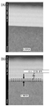
다음으로, 산소 도핑 처리를 실시하기 전과 산소 도핑을 실시한 후의 실리콘 웨이퍼의 단면을 STEM(Scanning Transmission Electron Microscopy)으로 관찰한 결과를 도 16에 나타낸다. 도 16(A)은, 산소 도핑 처리를 실시하기 전의 STEM상이며, 도 16(B)은, 상술한 RF 바이어스 전력 300 W의 조건으로 산소 도핑 처리를 실시한 후의 STEM상이다. 도 16(B)에 나타내는 바와 같이, 산소 도핑을 실시함에 의해, 실리콘 웨이퍼에 산소고도핑 영역이 형성되어 있는 것을 확인할 수 있다.Next, the cross section of the silicon wafer before and after the oxygen doping treatment was observed by STEM (Scanning Transmission Electron Microscopy) is shown in Fig. FIG. 16A is an STEM image before the oxygen doping process, and FIG. 16B is an STEM image after the oxygen doping process is performed under the condition of the RF bias power of 300 W described above. As shown in FIG. 16 (B), by performing oxygen doping, it can be confirmed that an oxygen highly doped region is formed in the silicon wafer.
이상과 같이, 실리콘 웨이퍼에 대하여 산소 도핑을 실시함으로써, 실리콘 웨이퍼에 산소가 첨가되는 것이 나타났다. 이 결과에 의해, 산화물 반도체막에 있어서 산소 도핑을 실시함에 의해서도, 산화물 반도체막에 산소를 당연히 첨가할 수 있는 것을 이해할 수 있다.As described above, when oxygen doping is performed on the silicon wafer, oxygen is added to the silicon wafer. It can be understood from this result that oxygen can be added to the oxide semiconductor film naturally even by performing oxygen doping in the oxide semiconductor film.
개시하는 발명의 일 태양인 상술한 구성의 효과는, 다음과 같이 생각하면 이해가 용이하다. 다만, 이하의 설명은, 어디까지나 한가지 고찰에 지나지 않는다는 것을 부기한다.The effect of the above-described configuration, which is one aspect of the disclosed invention, can be easily understood by considering the following. It should be noted, however, that the following description is merely a consideration.
게이트 전극에 플러스의 전압을 인가하면, 산화물 반도체막의 게이트 전극측으로부터 백채널측(게이트 절연막과 반대측)으로 전계가 발생하기 때문에, 산화물 반도체막중에 존재하는 플러스의 전하를 갖는 수소이온이 백채널측으로 이동하여, 산화물 반도체막과 절연막과의 계면중에서 산화물 반도체막측으로 축적한다. 축적한 수소이온으로부터 절연막중의 전하 포획 중심(수소 원자, 물, 혹은 오염물 등)에 플러스의 전하가 이동함으로써, 산화물 반도체막의 백채널 측에는 마이너스의 전하가 축적된다. 즉, 트랜지스터의 백채널 측으로 기생 채널이 발생하여, 스레숄드 전압이 마이너스측으로 시프트하여, 트랜지스터가 노멀리온(normally on)의 경향을 나타낸다.When a positive voltage is applied to the gate electrode, an electric field is generated from the gate electrode side to the back channel side (opposite to the gate insulating film) of the oxide semiconductor film. Therefore, hydrogen ions having a positive charge existing in the oxide semiconductor film And accumulates on the oxide semiconductor film side in the interface between the oxide semiconductor film and the insulating film. A positive charge moves from the accumulated hydrogen ions to the charge trapping centers (hydrogen atoms, water, or contaminants, etc.) in the insulating film, so that negative charges are accumulated on the back channel side of the oxide semiconductor film. That is, a parasitic channel is generated on the back channel side of the transistor, the threshold voltage shifts to the minus side, and the transistor shows a tendency of normally on.
상기한 바와 같이, 절연막중의 수소 또는 물 등의 전하 포획 중심이 플러스의 전하를 포획하여, 절연막중에 플러스의 전하가 이동함으로써 트랜지스터의 전기적 특성이 변동하기 때문에, 트랜지스터의 전기적 특성의 변동을 억제하기 위해서는, 절연막중에 이러한 전하 포획 중심이 존재하지 않거나, 또는 그 함유량이 적은 것이 중요하다. 따라서, 절연막의 성막에는, 성막시에 수소 함유량이 적은 스퍼터법을 이용하는 것이 바람직하다. 스퍼터법에 의해 성막된 절연막은, 그 막중에 전하 포획 중심이 존재하지 않거나, 또는 적고, CVD법 등에 의해 성막하였을 경우와 비교하여 플러스의 전하의 이동이 일어나기 어렵다. 따라서, 트랜지스터의 스레숄드 전압의 시프트를 억제하여, 트랜지스터를 노멀리 오프(normally off)로 할 수가 있다.As described above, the charge trapping centers of hydrogen or water in the insulating film capture the positive charge, and the positive electric charge moves into the insulating film, so that the electrical characteristics of the transistor fluctuate. Therefore, fluctuation of the electrical characteristics of the transistor is suppressed It is important that the charge trapping centers do not exist in the insulating film or the content thereof is small. Therefore, it is preferable to use a sputtering method with a small hydrogen content at the time of film formation for forming the insulating film. The insulating film formed by the sputtering method is less liable to cause positive charge transfer as compared with the case where the charge trapping center is not present in the film, or the film is formed by the CVD method or the like. Therefore, the shift of the threshold voltage of the transistor can be suppressed, and the transistor can be turned off normally (normally off).
또한, 탑게이트형의 트랜지스터에 있어서는, 기초가 되는 절연막상에 산화물 반도체막을 형성한 후, 열처리를 실시함으로써, 산화물 반도체막에 포함되는 물 또는 수소를 제거하는 것과 동시에, 절연막중에 포함되는 물 또는 수소도 제거할 수가 있다. 따라서, 절연막중에는, 산화물 반도체막중을 이동해 온 플러스의 전하를 포획하기 위한 전하 포획 중심이 적다. 이와 같이, 산화물 반도체막으로의 탈수화 또는 탈수소화를 위한 열처리는, 산화물 반도체막에 부가하여, 산화물 반도체막의 하층에 존재하는 절연막에 대하여도 행해지기 때문에, 탑게이트형의 트랜지스터에 있어서는, 기초가 되는 절연막은 플라즈마 CVD법 등의 CVD법을 이용하여 성막되어 있어도 상관없다.In the top gate type transistor, the oxide semiconductor film is formed on the underlying insulating film and then subjected to a heat treatment to remove water or hydrogen contained in the oxide semiconductor film, and water or hydrogen Can also be removed. Therefore, in the insulating film, the charge capturing centers for trapping the positive charges which have moved in the oxide semiconductor film are small. As described above, the heat treatment for dehydration or dehydrogenation into the oxide semiconductor film is also performed on the insulating film existing in the lower layer of the oxide semiconductor film in addition to the oxide semiconductor film. Therefore, in the top gate type transistor, May be formed by a CVD method such as a plasma CVD method.
또한, 게이트 전극에 마이너스의 전압을 인가하면, 백채널측으로부터 게이트 전극측으로 전계가 발생하기 때문에, 산화물 반도체막중에 존재하는 수소이온이 게이트 절연막측으로 이동하여, 산화물 반도체막과 게이트 절연막과의 계면중 산화물 반도체막측으로 축적한다. 또한, 이에 의해 트랜지스터의 스레숄드 전압은 마이너스측으로 시프트한다.When a negative voltage is applied to the gate electrode, an electric field is generated from the back channel side to the gate electrode side. Therefore, the hydrogen ions present in the oxide semiconductor film move toward the gate insulating film side and the interface between the oxide semiconductor film and the gate insulating film And accumulates on the oxide semiconductor film side. Further, the threshold voltage of the transistor thereby shifts to the minus side.
또한, 전압을 0으로서 방치하면, 전하 포획 중심으로부터 플러스의 전하가 해방되어 트랜지스터의 스레숄드 전압이 플러스측으로 시프트하여, 초기 상태로 돌아오거나, 또는 경우에 따라서는 초기 상태보다 플러스측으로 시프트한다. 이 현상은, 산화물 반도체막중으로 이동하기 쉬운 이온이 존재하고 있다는 것을 시사하고 있으며, 가장 작은 원자인 수소가 가장 이동하기 쉬운 이온이 된다고 고찰할 수가 있다.Also, when the voltage is left at 0, the positive charge is released from the charge trapping center, and the threshold voltage of the transistor shifts to the positive side and returns to the initial state or, in some cases, shifts to the positive side more than the initial state. This phenomenon suggests that ions that are liable to migrate into the oxide semiconductor film exist, and it can be considered that hydrogen as the smallest atom is the most easily transportable ion.
또한, 산화물 반도체막이 광을 흡수함으로써, 광 에너지에 의해 산화물 반도체막중의 금속 원소(M)와 수소 원자(H)와의 결합(M-H결합이라고도 표기한다)이 끊어진다. 또한 파장이 400 nm 전후의 광 에너지와 금속 원소 및 수소 원자의 결합 에너지와는 대략 일치하고 있다. 산화물 반도체막중의 금속 원소와 수소 원자와의 결합이 끊어진 트랜지스터에 음의 게이트 바이어스를 가하면, 금속 원소로부터 이탈한 수소이온이 게이트 전극 측으로 끌어 당겨질 수 있기 때문에 전하의 분포가 변화하고, 트랜지스터의 스레숄드 전압은 마이너스 측으로 시프트하여, 노멀리온의 경향을 나타낸다.Further, the oxide semiconductor film absorbs light, so that the bond (also referred to as M-H bond) between the metal element M and the hydrogen atom H in the oxide semiconductor film is broken by the light energy. And the light energy of the wavelength around 400 nm and the binding energy of the metal element and the hydrogen atom substantially coincide with each other. When a negative gate bias is applied to a transistor in which a bond between a metal element and a hydrogen atom in the oxide semiconductor film is broken, the hydrogen ions desorbed from the metal element can be attracted to the gate electrode side, so that the charge distribution changes, Is shifted to the minus side and shows the tendency of normal lean.
또한, 트랜지스터로의 광조사와 음의 게이트 바이어스의 인가에 의해 게이트 절연막 계면으로 이동한 수소이온은, 전압의 인가를 정지하면 원래대로 돌아간다. 이것은, 산화물 반도체막중의 이온 이동의 대표적인 예로서 이해할 수 있다.Further, the hydrogen ions migrating to the interface of the gate insulating film due to the light irradiation to the transistor and the application of the negative gate bias return to the original state when the application of the voltage is stopped. This can be understood as a representative example of ion migration in the oxide semiconductor film.
이러한, 전압 인가에 의한 전기적 특성의 변동(BT열화) 또는 광조사에 의한 전기적 특성의 변동(광열화)에의 대책은, 산화물 반도체막으로부터 수소 원자 또는 물 등의 수소 원자를 포함한 불순물을 철저하게 배제하여, 산화물 반도체막을 고순도화하는 것이 가장 중요하다. 전하 밀도가 1015 cm-3, 즉, 단위면적 당의 전하가 1010 cm-2의 경우, 그 전하는 트랜지스터 특성에 영향을 주지 않거나 또는 영향을 준다고 하더라도 매우 적다. 따라서, 전하 밀도는 1015 cm-3 이하인 것이 바람직하다. 만일, 산화물 반도체막에 포함되는 수소 중에, 10%의 수소가 산화물 반도체막중을 이동하는 경우, 수소의 농도는 1016 cm-3 이하인 것이 바람직하다. 게다가 디바이스 완성 후에 수소가 외부에서 침입하는 것을 막기 위해서, 스퍼터법에 따라서 성막한 질화 실리콘막을 패시베이션막으로서 이용하여 트랜지스터를 덮는 것이 바람직하다.Such countermeasures against the fluctuation of the electrical characteristics (BT deterioration) by the voltage application or the fluctuation of the electrical characteristics (light deterioration) by the irradiation of light are to thoroughly remove impurities including hydrogen atoms or hydrogen atoms from the oxide semiconductor film Thus, it is most important that the oxide semiconductor film is highly purified. When the charge density is 10 15 cm -3 , that is, the charge per unit area is 10 10 cm -2 , the charge does not affect the transistor characteristics or is very small even if it affects the transistor characteristics. Therefore, the charge density is preferably 10 15 cm -3 or less. If 10% of hydrogen moves in the oxide semiconductor film in the hydrogen contained in the oxide semiconductor film, the concentration of hydrogen is preferably 10 16 cm -3 or less. Furthermore, in order to prevent hydrogen from intruding from the outside after the completion of the device, it is preferable to cover the transistor by using a silicon nitride film formed by a sputtering method as a passivation film.
게다가 산화물 반도체막중에 포함되는 수소에 대하여, 과잉의 산소를 도핑함((수소 원자의 수)≪(산소 라디칼의 수) 또는, (산소 이온의 수)로 한다)으로써, 산화물 반도체막으로부터 수소 또는 물을 배제할 수가 있다. 구체적으로는, 고주파(RF)를 이용하여 산소를 플라즈마화하고, 기판 바이어스를 크게 하여, 산소 라디칼, 산소 이온을 기판상의 산화물 반도체막에 도핑 또는 첨가하여, 산화물 반도체막중에서는 잔존하는 수소보다 산소를 많게 한다. 산소의 전기 음성도는 3.0로서 전기 음성도가 약 2.0인 산화물 반도체막중의 금속(Zn, Ga, In)보다 크기 때문에, 수소에 대하여 산소를 과잉으로 함유시킴으로써, M-H기로부터 수소를 빼앗아, OH기를 형성한다. 또한 이 OH기는, M와 결합하여 M-O-H기를 형성할 수 있다.(Hydrogen atoms) " (oxygen radicals) or (oxygen ions)) with respect to hydrogen contained in the oxide semiconductor film, Water can be excluded. Specifically, oxygen is made plasma by using a high frequency (RF), the substrate bias is increased, and oxygen radicals and oxygen ions are doped or added to the oxide semiconductor film on the substrate. In the oxide semiconductor film, oxygen Do a lot. Since the electronegativity of oxygen is larger than that of the metal (Zn, Ga, In) in the oxide semiconductor film having an electronegativity of about 2.0 and an electronegativity of about 2.0, oxygen is excessively contained in hydrogen, . This OH group can also combine with M to form an M-O-H group.
또한, 산화물 반도체막의 산소의 함유량이, 화학량론비보다 과잉이 되도록 산소를 도핑하는 것이 보다 바람직하다. 예를 들면, 산화물 반도체막으로서 In-Ga-Zn-O계 산화물 반도체막을 이용하는 경우, 산소의 도핑 등에 의해 산소의 비율을 화학량론비의 1배를 넘어 2배까지(2배 미만)로 하는 것이 보다 바람직하다. 예를 들면, In-Ga-Zn-O계 산화물 반도체의 단결정의 화학량론비를 In:Ga:Zn:O=1:1:1:4로 하면, 조성이 InGaZnOx로 나타내어지는 산화물 반도체 박막에 있어서, X는 4를 넘어 8 미만으로 하는 것이 보다 바람직하다. 따라서, 산화물 반도체막에 있어서 산소의 함유량은 수소의 함유량보다 커진다.Further, it is more preferable to dope oxygen so that the content of oxygen in the oxide semiconductor film is larger than the stoichiometric ratio. For example, when an In-Ga-Zn-O-based oxide semiconductor film is used as the oxide semiconductor film, it is preferable to make the ratio of oxygen to 1: 2 or more (less than 2 times) desirable. For example, assuming that the stoichiometric ratio of a single crystal of an In-Ga-Zn-O based oxide semiconductor is In: Ga: Zn: O = 1: 1: 1: 4, in an oxide semiconductor thin film represented by InGaZnO x , , And X is preferably more than 4 and less than 8. Therefore, the content of oxygen in the oxide semiconductor film is larger than the content of hydrogen.
광 에너지나 BT스트레스에 의해, M-H기로부터 수소가 이탈해 열화의 원인이 되지만, 상술한 도핑에 의해 산소를 주입하는 경우, 주입된 산소가 수소이온과 결합하여 OH기가 된다. OH기는, 결합 에너지가 크기 때문에, 트랜지스터에 광조사나 BT스트레스가 가해져도 수소이온을 방출하지 않고, 또한 수소이온보다 질량도 크기 때문에, 산화물 반도체막중을 이동하기 어렵다. 따라서, 산소의 도핑에 기인하여 형성되는 OH기는, 트랜지스터의 열화의 원인이 되지 않던지, 또는 열화의 원인을 줄일 수가 있다.Hydrogen is released from the M-H group by light energy or BT stress to cause deterioration. When oxygen is injected by the above-described doping, the injected oxygen combines with hydrogen ions to become an OH group. The OH group does not release hydrogen ions even when light intensity modulation or BT stress is applied to the transistor because of its large binding energy, and it is difficult to move the oxide semiconductor film because the OH group has a larger mass than hydrogen ions. Therefore, the OH group formed due to the doping of oxygen does not cause deterioration of the transistor or can reduce the cause of deterioration.
또한, 산화물 반도체막의 막두께를 크게 할수록, 트랜지스터의 스레숄드 전압이 불규칙해지는 경향이 확인되고 있다. 이것은, 산화물 반도체막중의 산소 결함이 스레숄드 전압의 변동의 한 요인이며, 막두께가 커질수록 그 산소 결함이 증가하기 때문이라고 추측할 수 있다. 본 발명의 일 태양과 관련되는 트랜지스터에 있어서 산화물 반도체막에 산소를 도핑하는 공정은, 산화물 반도체막으로부터의 수소 또는 물의 배제뿐만 아니라, 막중의 산소 결함의 보충에 대하여도 유효하다. 따라서, 본 발명의 일 태양과 관련되는 트랜지스터는, 스레숄드 전압의 편차도 제어할 수가 있다.Further, it has been confirmed that as the film thickness of the oxide semiconductor film is increased, the threshold voltage of the transistor becomes irregular. This is presumably because the oxygen defects in the oxide semiconductor film are a factor of the fluctuation of the threshold voltage, and the oxygen defects increase as the film thickness increases. The step of doping the oxide semiconductor film with oxygen in the transistor according to an aspect of the present invention is effective not only for elimination of hydrogen or water from the oxide semiconductor film but also for supplementation of oxygen defects in the film. Therefore, the transistor relating to one aspect of the present invention can also control the deviation of the threshold voltage.
또한, 산화물 반도체막을 사이에 끼워서, 산화물 반도체막과 동종의 성분으로 이루어지는 금속 산화물막을 마련하는 구성도, 전기적 특성의 변동 방지에 효과적이다. 산화물 반도체막과 동종의 성분으로 이루어지는 금속 산화물막으로서, 구체적으로는, 산화물 반도체막의 성분 원소로부터 선택되는 1종 또는 복수의 금속 원소의 산화물을 포함한 막을 이용하는 것이 바람직하다. 이러한 재료는 산화물 반도체막과의 상성(相性)이 좋고, 산화물 반도체막을 사이에 끼워서 그 금속 산화물막을 마련함으로써, 산화물 반도체막과의 계면 상태를 양호하게 유지할 수가 있다. 즉, 상술한 재료를 이용한 금속 산화물막을, 산화물 반도체막과 접하는 절연막으로서 마련함으로써, 그 금속 산화물막과 산화물 반도체막과의 계면 및 그 근방으로의 수소이온의 축적을 억제 또는 방지할 수가 있다. 따라서, 산화물 반도체막을 사이에 끼워서, 예를 들면, 산화 실리콘막 등의 산화물 반도체막과는 다른 성분으로 이루어지는 절연막을 마련했을 경우와 비교하여, 트랜지스터의 스레숄드 전압에 영향을 주는 산화물 반도체막 계면의 수소 농도를 충분히 저감할 수가 있다.Further, the structure in which the oxide semiconductor film is sandwiched between the oxide semiconductor film and the metal oxide film composed of the same kind of component as the oxide semiconductor film is also effective in preventing fluctuation of electrical characteristics. It is preferable to use a film containing an oxide of one or more metal elements selected from the constituent elements of the oxide semiconductor film as the metal oxide film composed of the same kind of components as the oxide semiconductor film. Such a material is good in phase with the oxide semiconductor film, and the interface state with the oxide semiconductor film can be well maintained by providing the oxide film with the oxide semiconductor film therebetween. That is, by providing the metal oxide film using the above-described material as an insulating film in contact with the oxide semiconductor film, accumulation of hydrogen ions at the interface between the metal oxide film and the oxide semiconductor film and in the vicinity thereof can be suppressed or prevented. Therefore, as compared with the case where an insulating film made of a different component from an oxide semiconductor film such as a silicon oxide film is provided with the oxide semiconductor film sandwiched therebetween, hydrogen at the interface of the oxide semiconductor film, which affects the threshold voltage of the transistor, The concentration can be sufficiently reduced.
또한, 그 금속 산화물막으로서는, 산화 갈륨막을 이용하는 것이 바람직하다. 산화 갈륨은, 밴드갭(Eg)이 크기 때문에, 산화 갈륨막에 의해 산화물 반도체막을 사이에 끼움으로써, 산화물 반도체막과 금속 산화물막과의 계면에서, 에너지 장벽이 형성되어 그 계면에 있어서 캐리어의 이동은 방해할 수 있다. 따라서, 캐리어는 산화물 반도체로부터 금속 산화물로 이동하는 일 없이, 산화물 반도체막중을 이동한다. 한편, 수소이온은, 산화물 반도체와 금속 산화물과의 계면을 통과하여, 금속 산화물과 절연막과의 계면 부근에 축적한다. 만일, 절연막과의 계면 근방에 수소이온이 축적되었다고 하여도, 금속 산화물막으로서의 산화 갈륨막에는 캐리어가 흐를 수 있는 기생 채널이 형성되지 않기 때문에, 트랜지스터의 스레숄드 전압에 대한 영향을 주지 않거나, 또는 그 영향이 극히 적다. 또한 산화 갈륨과 In-Ga-Zn-O계의 재료를 접촉시켰을 경우의 에너지 장벽은, 전도대측에서 약 0.8 eV가 되며, 가전자대측에서 약 0.9 eV가 된다.As the metal oxide film, it is preferable to use a gallium oxide film. Since gallium oxide has a large band gap Eg, an energy barrier is formed at the interface between the oxide semiconductor film and the metal oxide film by sandwiching the oxide semiconductor film therebetween by the gallium oxide film, Can interfere. Therefore, the carrier moves in the oxide semiconductor film without moving from the oxide semiconductor to the metal oxide. On the other hand, the hydrogen ions pass through the interface between the oxide semiconductor and the metal oxide, and accumulate near the interface between the metal oxide and the insulating film. Even if hydrogen ions are accumulated in the vicinity of the interface with the insulating film, no parasitic channel is formed in the gallium oxide film as a metal oxide film, so that the carrier does not affect the threshold voltage of the transistor, Influence is extremely small. When the gallium oxide and the In-Ga-Zn-O-based material are brought into contact with each other, the energy barrier becomes about 0.8 eV on the conduction band side and about 0.9 eV on the valence band side.
개시하는 발명의 일 태양과 관련되는 트랜지스터는, 산소 도핑 처리에 의해, 산화물 반도체막에 접하는 절연막중, 산화물 반도체막중, 또는 이러한 계면 근방중의 적어도 어느 하나에 산소의 함유량을 증대시키는 것을 기술 사상으로 하는 것이다.The transistor relating to one aspect of the disclosed invention is characterized in that the oxygen content is increased in at least one of the insulating film in contact with the oxide semiconductor film, the oxide semiconductor film, or the vicinity of the interface by oxygen doping treatment .
산화물 반도체막으로서 인듐을 포함한 산화물 반도체 재료를 이용하는 경우, 인듐과 산소의 결합력은 비교적 약하기 때문에, 산화물 반도체막에 접하는 절연막에 실리콘 등의 산소와의 결합력이 보다 강한 재료가 포함되는 경우에, 열처리에 의해 산화물 반도체막중의 산소가 빠져버려서, 산화물 반도체막의 계면 근방에 산소 결손이 형성될 우려가 있다. 그렇지만, 개시하는 발명의 일 태양과 관련되는 트랜지스터는, 산화물 반도체막에 과잉의 산소를 공급함으로써, 산소 결손의 형성을 억제할 수가 있다.When an oxide semiconductor material containing indium is used as the oxide semiconductor film, the bonding force between indium and oxygen is comparatively weak. Therefore, when the insulating film in contact with the oxide semiconductor film contains a material having stronger bonding force with oxygen such as silicon, Oxygen in the oxide semiconductor film is lost by the oxidation, and there is a fear that an oxygen defect is formed in the vicinity of the interface of the oxide semiconductor film. However, the transistor relating to one aspect of the disclosed invention can suppress the formation of oxygen deficiency by supplying excess oxygen to the oxide semiconductor film.
여기서, 트랜지스터의 제작 공정에 있어서 산소 도핑 처리를 실시한 다음에는, 산화물 반도체막 또는 산화물 반도체막에 접하는 절연막에 함유되는, 화학량론비보다 과잉의 산소량이 각층에서 다른 경우가 있다. 과잉의 산소량이 다른 상태에서는, 각층의 산소의 화학 퍼텐셜이 다르며, 화학 퍼텐셜의 차이는 트랜지스터의 제작 공정에 있어서의 열처리 등으로, 평형 상태에 가까워지거나, 또는 평형 상태가 된다고 생각된다. 이하에서는, 평형 상태에 있어서의 산소의 분포에 대하여 검토한다.Here, after the oxygen doping process is performed in the manufacturing process of the transistor, the amount of oxygen contained in the insulating film in contact with the oxide semiconductor film or the oxide semiconductor film is different from that of the respective layers in terms of the stoichiometric ratio. It is considered that the chemical potentials of oxygen in the respective layers are different from each other when the excess amount of oxygen is different and the difference in chemical potential is close to the equilibrium state or the equilibrium state due to the heat treatment in the manufacturing process of the transistor. Hereinafter, the distribution of oxygen in an equilibrium state will be studied.
어느 온도 T, 압력 P에서의 평형 상태란, 전계의 깁스의 자유에너지 G가 최소가 되는 상태이며, 이하의 식(1)으로 나타내어진다.The equilibrium state at a certain temperature T and the pressure P means a state in which the free energy G of the electric field gemini is minimized and is represented by the following equation (1).

식(1)에 있어서, G(1), G(2), G(3)는, 각층의 깁스의 자유에너지를 나타낸다. 또한, Na, Nb, Nc는 입자수를 나타내며, a, b, c는 입자의 종류를 나타낸다. 입자 a가 i층으로부터 j층으로δNa(j)만큼 이동했을 경우, 깁스의 자유에너지의 변화는, 이하의 식(2)과 같이 된다.In equation (1), G (1) , G (2) , and G (3) represent the free energy of the gibbs of each layer. In addition, N a , N b , and N c represent the number of particles, and a, b, and c represent the types of particles. When the particle a moves from the i-th layer to the j-th layer by delta Na (j) , the change of the free energy of the gibbles is expressed by the following formula (2).

여기서, δG가 0, 즉 이하의 식(3)이 성립될 때, 계가 평형 상태가 된다.Here, when? G is 0, that is, when the following formula (3) is established, the system becomes in an equilibrium state.

깁스의 자유에너지의 입자수 미분은, 화학 퍼텐셜에 상당하므로, 평형 상태에 있어서, 입자의 화학 퍼텐셜이 모든 층에서 동일해진다.Since the particle number differential of free energy of Gibbs corresponds to the chemical potential, the chemical potential of the particles becomes equal in all layers in an equilibrium state.
즉, 구체적으로는, 절연막과 비교하여 산화물 반도체막에 산소가 과잉으로 포함되어 있는 경우, 절연막에서는 산소의 화학 퍼텐셜이 상대적으로 작고, 산화물 반도체막에서는 화학 퍼텐셜이 상대적으로 큰 상태가 되어 있다.Specifically, when oxygen is excessively contained in the oxide semiconductor film as compared with the insulating film, the chemical potential of oxygen is relatively small in the insulating film, and the chemical potential is relatively large in the oxide semiconductor film.
그리고, 트랜지스터의 제작 공정에 있어서 열처리를 실시함으로써, 계 전체(여기에서는, 산화물 반도체막과 거기에 접하는 절연막)가 충분히 고온이 되어, 원자의 층내 및 층간의 확산이 일어나게 되면, 화학 퍼텐셜이 같아지도록 산소의 이동이 일어난다. 즉, 산화물 반도체막의 산소가 절연막으로 이동함으로써, 산화물 반도체막의 화학 퍼텐셜이 작아지고, 절연막의 화학 퍼텐셜이 커진다.Then, heat treatment is performed in the manufacturing process of the transistor so that the entire system (here, the oxide semiconductor film and the insulating film in contact with the oxide semiconductor film) becomes sufficiently high temperature so that the chemical potential is equalized Oxygen migration occurs. That is, as the oxygen of the oxide semiconductor film moves to the insulating film, the chemical potential of the oxide semiconductor film becomes small, and the chemical potential of the insulating film becomes large.
따라서, 산소 도핑 처리에 의해 산화물 반도체막에 과잉으로 공급된 산소는, 그 후의 열처리에 의해 계내의 화학 퍼텐셜을 평형 상태로 함으로써, 확산하여, 절연막(계면을 포함한다)에 공급된다. 이 때문에, 산화물 반도체막에 과잉의 산소가 충분히 존재하는 경우에는, 산화물 반도체막에 접하는 절연막(계면을 포함한다)도 산소 과잉으로 할 수 있다.Therefore, the oxygen excessively supplied to the oxide semiconductor film by the oxygen doping treatment diffuses by making the chemical potential in the system equilibrium by the subsequent heat treatment, and is supplied to the insulating film (including the interface). Therefore, when oxygen is sufficiently present in the oxide semiconductor film, the insulating film (including the interface) in contact with the oxide semiconductor film can also be excessively oxygenated.
따라서, 절연막이나 절연막과의 계면에 있어서의 산소 부족 결함을 보상하는데 충분한 양(산소 부족 결함을 보상하여도 여유가 있는 과잉의 양)의 산소를 산화물 반도체막중에 공급해 두는 것에는 큰 의의가 있다고 말할 수 있다.Therefore, it is said that it is of great significance to supply enough oxygen in the oxide semiconductor film in an amount sufficient to compensate for the oxygen deficiency defect at the interface with the insulating film or the insulating film (an excessive amount of margin, which is sufficient to compensate for the oxygen deficiency defect) .
열처리에 의한 탈수화 또는 탈수소화 처리, 및 산소 도핑 처리된 산화물 반도체막을 갖는 트랜지스터는, 바이어스-열스트레스(BT) 시험 전후에도 트랜지스터의 스레숄드 전압의 변화량이 저감되어 있어, 안정된 전기 특성을 갖는 신뢰성이 높은 트랜지스터를 실현할 수 있다.The transistor having the oxide semiconductor film subjected to the dehydration or dehydrogenation treatment by the heat treatment and the oxygen doping treatment has a reduced amount of change in the threshold voltage of the transistor even before and after the bias-thermal stress (BT) test, A high transistor can be realized.
또한, 개시하는 발명의 일 태양에 의해, 전기 특성이 양호하여 신뢰성이 높은 트랜지스터를 갖는 여러 가지 반도체 장치를 제작할 수가 있다.In addition, according to one aspect of the disclosed invention, various semiconductor devices having a transistor with good electrical characteristics and high reliability can be manufactured.
도 1은 반도체 장치의 일 형태를 설명하는 도.
도 2는 반도체 장치의 제작 방법의 일 형태를 설명하는 도.
도 3은 반도체 장치의 형태를 설명하는 도.
도 4는 반도체 장치의 제작 방법의 일 형태를 설명하는 도.
도 5는 반도체 장치의 제작 방법의 일 형태를 설명하는 도.
도 6은 반도체 장치의 제작 방법 일 형태를 설명하는 도.
도 7은 반도체 장치의 단면도, 표면도 및 회로도.
도 8은 반도체 장치의 일 형태를 설명하는 도.
도 9는 반도체 장치의 일 형태를 설명하는 도.
도 10은 반도체 장치의 일 형태를 설명하는 도.
도 11은 반도체 장치의 일 형태를 설명하는 도.
도 12는 반도체 장치의 일 태양을 설명하는 도.
도 13은 전자기기를 나타내는 도.
도 14는 전자기기를 나타내는 도.
도 15는 SIMS의 측정 결과를 나타내는 도.
도 16은 단면 STEM상을 설명하는 도.
도 17은 플라즈마 장치의 표면도 및 단면도.BRIEF DESCRIPTION OF THE DRAWINGS Fig. 1 is a view for explaining one embodiment of a semiconductor device;
BACKGROUND OF THE INVENTION 1. Field of the Invention [0001]
3 is a diagram illustrating a configuration of a semiconductor device;
4 is a view for explaining an embodiment of a manufacturing method of a semiconductor device.
5 is a view for explaining an embodiment of a method of manufacturing a semiconductor device.
6 is a view for explaining one form of a method for manufacturing a semiconductor device;
7 is a cross-sectional view, a surface view, and a circuit diagram of the semiconductor device.
8 is a view for explaining an embodiment of a semiconductor device.
9 is a view for explaining an embodiment of a semiconductor device.
10 is a view for explaining an embodiment of a semiconductor device;
11 is a view for explaining an embodiment of a semiconductor device.
12 is a view for explaining an aspect of a semiconductor device;
13 is a view showing an electronic apparatus;
14 is a view showing an electronic device.
15 is a view showing a measurement result of SIMS;
16 is a view for explaining a sectional STEM image;
17 is a top view and a cross-sectional view of the plasma apparatus.
이하에서는, 본 명세서에 개시하는 발명의 실시형태에 대하여 도면을 이용하여 상세하게 설명한다. 다만, 본 명세서에 개시하는 발명은 이하의 설명에 한정되지 않고, 그 형태 및 상세를 여러 가지로 변경할 수 있다는 것은, 당업자라면 용이하게 이해된다. 또한, 본 명세서에 개시하는 발명은 이하에 나타내는 실시형태의 기재 내용에 한정하여 해석되는 것은 아니다.Hereinafter, embodiments of the invention disclosed in the present specification will be described in detail with reference to the drawings. It is to be understood by those skilled in the art, that the invention disclosed herein is not limited to the following description, and that various changes in form and detail may be made therein. The invention disclosed in this specification is not limited to the content of the embodiments described below.
또한, 본 명세서 등에 있어서의 「제 1」, 「제 2」, 「제 3」 등의 서수사는, 구성요소의 혼동을 피하기 위해서 붙인 것이며, 수적으로 한정하는 것이 아니라는 것을 부기한다.It should be noted that ordinal numbers such as "first", "second", "third", etc. in the present specification are added for avoiding confusion of components, and are not limited to numerals.
(실시형태 1)(Embodiment 1)
본 실시형태에서는, 반도체 장치 및 반도체 장치의 제작 방법에 대하여, 도 1 내지 도 3을 이용하여 설명한다.In this embodiment, a method of manufacturing a semiconductor device and a semiconductor device will be described with reference to Figs. 1 to 3. Fig.
<반도체 장치의 구성예><Configuration Example of Semiconductor Device>
도 1에는, 트랜지스터(120)의 구성예를 나타낸다. 여기서, 도 1(A)은 평면도이며, 도 1(B) 및 도 1(C)은 각각, 도 1(A)에 있어서의 A-B 단면 및 C-D 단면과 관련되는 단면도이다. 또한 도 1(A)에서는 번잡하게 되는 것을 피하기 위해, 트랜지스터(120)의 구성요소의 일부(예를 들면, 게이트 절연막(110) 등)를 생략하고 있다.Fig. 1 shows a configuration example of the
도 1에 나타내는 트랜지스터(120)는, 기판(100)상의 절연막(102), 소스 전극(104a), 드레인 전극(104b), 산화물 반도체막(108), 게이트 절연막(110), 게이트 전극(112)을 포함한다.The
도 1에 나타내는 트랜지스터(120)에 있어서, 산화물 반도체막(108)은, 산소 도핑 처리를 한 산화물 반도체막이다. 산소 도핑 처리를 함으로써, 신뢰성이 높아진 트랜지스터(120)가 실현된다.In the
<반도체 장치의 제작 공정예><Example of Fabrication Process of Semiconductor Device>
이하, 도 2를 이용하여, 도 1에 나타내는 반도체 장치의 제작 공정의 일 예를 설명한다.Hereinafter, an example of a manufacturing process of the semiconductor device shown in Fig. 1 will be described with reference to Fig.
우선, 기판(100)상에 절연막(102)을 형성한다(도 2(A) 참조).First, an insulating
기판(100)의 재질 등에 큰 제한은 없지만, 적어도, 후의 열처리에 견디는 정도의 내열성을 갖고 있을 것이 필요하다. 예를 들면, 유리 기판, 세라믹 기판, 석영 기판, 사파이어 기판 등을, 기판(100)으로서 이용할 수가 있다. 또한, 실리콘이나 탄화 실리콘 등의 단결정 반도체 기판, 다결정 반도체 기판, 실리콘 게르마늄 등의 화합물 반도체 기판, SOI 기판 등을 적용하는 것도 가능하고, 이러한 기판상에 반도체소자가 마련된 것을, 기판(100)으로서 이용하여도 괜찮다.There is no particular limitation on the material of the
또한, 기판(100)으로서 가요성 기판을 이용하여도 괜찮다. 가요성 기판상에 트랜지스터를 마련하는 경우, 가요성 기판상에 직접적으로 트랜지스터를 만들어도 괜찮고, 다른 기판에 트랜지스터를 형성한 후, 이를 박리하고, 가요성 기판에 전치(轉置)하여도 좋다. 또한 트랜지스터를 박리하고, 가요성 기판에 전치하기 위해서는, 상기 다른 기판과 트랜지스터와의 사이에 박리층을 형성하면 좋다.Further, a flexible substrate may be used as the
절연막(102)은 기초로서 기능하는 절연막이다. 구체적으로는, 절연막(102)에는, 산화 실리콘, 질화 실리콘, 산화 알루미늄, 질화 알루미늄, 산화 갈륨, 이들의 혼합 재료 등을 이용하면 좋다. 또한, 절연막(102)은, 상술한 재료를 포함한 절연막의 단층 구조로 하여도 좋고, 적층 구조로 하여도 좋다.The insulating
절연막(102)의 제작 방법에 특별히 한정은 없다. 예를 들면, 플라즈마 CVD법이나 스퍼터링법 등의 성막 방법을 이용하여 절연막(102)을 제작할 수가 있다. 또한 수소나 물 등이 혼입하기 어렵다고 하는 점에서는, 스퍼터링법이 매우 적합하다.The method for manufacturing the insulating
또한, 절연막(102)에는, 후에 형성되는 산화물 반도체막과 동종의 성분으로 이루어지는 절연 재료를 이용하면 특히 바람직하다. 이러한 재료는 산화물 반도체막과의 상성이 좋고, 이를 절연막(102)에 이용함으로써, 산화물 반도체막과의 계면 상태를 양호하게 유지할 수가 있기 때문이다. 여기서, 「산화물 반도체막과 동종의 성분」이란, 산화물 반도체막의 성분 원소로부터 선택되는 1종 또는 복수의 원소를 의미한다. 예를 들면, 산화물 반도체막이 In-Ga-Zn-O계의 산화물 반도체 재료에 의해 구성되는 경우, 동종의 성분으로 이루어지는 절연 재료로서는 산화 갈륨 등이 있다.It is particularly preferable to use an insulating material composed of the same kind of material as the oxide semiconductor film to be formed later in the insulating
또한, 절연막(102)을 적층 구조로 하는 경우에는, 산화물 반도체막과 동종의 성분으로 이루어지는 절연 재료로 이루어지는 막(이하, 막a)과, 막a의 성분 재료와는 다른 재료를 포함한 막(이하, 막b)의 적층 구조로 하면 더욱 좋다. 막a와 막b를 산화물 반도체막측으로부터 순서대로 적층한 구조로 함으로써, 전하는 막a와 막b의 계면의 전하 포획 중심에 우선적으로 포획되기(산화물 반도체막과 막a의 계면과의 비교) 때문에, 산화물 반도체막의 계면에서의 전하 포획을 충분히 억제할 수가 있게 되어, 반도체 장치의 신뢰성이 향상하기 때문이다.When the insulating
또한, 이러한 적층 구조로서는, 산화 갈륨막과 산화 실리콘막의 적층 구조나, 산화 갈륨막과 질화 실리콘막의 적층 구조 등을 적용할 수가 있다.As the laminated structure, a laminated structure of a gallium oxide film and a silicon oxide film, a laminated structure of a gallium oxide film and a silicon nitride film, and the like can be applied.
그 다음으로, 절연막(102)상에, 소스 전극 및 드레인 전극(이와 동일한 층에서 형성되는 배선을 포함한다)을 형성하기 위한 도전막을 형성하고, 해당 도전막을 가공하여, 소스 전극(104a) 및 드레인 전극(104b)을 형성한다(도 2(B) 참조). 또한 여기서 형성되는 소스 전극(104a)의 단부와 드레인 전극(104b)의 단부의 간격에 의해, 트랜지스터의 채널장(L)이 결정되게 된다.Next, a conductive film for forming a source electrode and a drain electrode (including wiring formed in the same layer) is formed on the insulating
소스 전극(104a) 및 드레인 전극(104b)에 이용하는 도전막으로서는, 예를 들면, Al, Cr, Cu, Ta, Ti, Mo, W로부터 선택된 원소를 포함한 금속막, 또는 상술한 원소를 성분으로 하는 금속 질화물막(질화 티탄막, 질화 몰리브덴막, 질화 텅스텐막) 등이 있다. 또한, Al, Cu 등의 금속막의 하측 또는 상측중의 한쪽 또는 양쪽에 Ti, Mo, W 등의 고융점 금속막 또는 이들의 금속 질화물막(질화 티탄막, 질화 몰리브덴막, 질화 텅스텐막)을 적층시킨 도전막을 이용하여도 좋다.As the conductive film used for the
또한, 소스 전극(104a) 및 드레인 전극(104b)에 이용하는 도전막은, 도전성의 금속 산화물로 형성하여도 좋다. 도전성의 금속 산화물로서는 산화 인듐(In2O3), 산화 주석(SnO2), 산화 아연(ZnO), 산화 인듐 산화 주석 합금(In2O3―SnO2, ITO로 약기한다), 산화 인듐 산화 아연 합금(In2O3―ZnO) 또는 이들의 금속 산화물 재료에 산화 실리콘을 포함시킨 것을 이용할 수가 있다.The conductive film used for the
도전막의 가공은, 레지스트 마스크를 이용한 에칭에 의해 실시할 수가 있다. 해당 에칭에 이용하는 레지스트 마스크 형성시의 노광에는, 자외선이나 KrF 레이저광이나 ArF 레이저광 등을 이용하면 좋다.The conductive film can be processed by etching using a resist mask. Ultraviolet light, KrF laser light, ArF laser light, or the like may be used for exposure in forming a resist mask used for the etching.
또한, 채널장(L)=25 nm 미만의 노광을 실시하는 경우에는, 예를 들면, 수 nm~수 10 nm로 극히 파장이 짧은 초자외선(Extreme Ultraviolet)을 이용하여, 레지스트 마스크 형성시의 노광을 실시하면 좋다. 초자외선에 의한 노광은, 해상도가 높고 초점심도도 크다. 따라서, 후에 형성되는 트랜지스터의 채널장(L)을 미세화하는 것이 가능하고, 회로의 동작 속도를 높일 수가 있다.In the case of performing exposure with a channel length L of less than 25 nm, exposure using a resist mask, for example, using ultraviolet light having a very short wavelength of several nm to several tens nm, . Exposure by ultraviolet rays has a high resolution and a large depth of focus. Therefore, the channel length L of the transistor to be formed later can be made finer, and the operation speed of the circuit can be increased.
또한, 이른바 다계조 마스크에 의해 형성된 레지스트 마스크를 이용하여 에칭 공정을 실시하여도 괜찮다. 다계조 마스크를 이용하여 형성된 레지스트 마스크는, 복수의 막두께를 갖는 형상이 되며, 애싱에 의해 더욱 형상을 변형시킬 수가 있기 때문에, 다른 패턴으로 가공하는 복수의 에칭 공정에 이용하는 것이 가능하다. 이 때문에, 한 장의 다계조 마스크에 의해, 적어도 2종류 이상의 다른 패턴에 대응하는 레지스트 마스크를 형성할 수가 있다. 즉, 공정의 간략화가 가능해진다.It is also possible to perform an etching process using a resist mask formed by a so-called multi-gradation mask. The resist mask formed by using the multi-gradation mask has a shape with a plurality of film thicknesses and can be further deformed by ashing, so that the resist mask can be used for a plurality of etching processes for processing into different patterns. Therefore, a resist mask corresponding to at least two different patterns can be formed by a single multi-gradation mask. That is, the process can be simplified.
다음으로, 절연막(102)상에, 소스 전극(104a) 및 드레인 전극(104b)과 접하는 산화물 반도체막을 형성하고, 해당 산화물 반도체막을 가공하여 섬 형상의 산화물 반도체막(106)을 형성한다(도 2(C) 참조).Next, an oxide semiconductor film which is in contact with the
산화물 반도체막은, 수소나 물 등이 혼입하기 어려운 방법으로 제작하는 것이 바람직하다. 예를 들면, 스퍼터링법 등을 이용하여 제작할 수가 있다. 또한, 산화물 반도체막의 두께는, 3 nm 이상 30 nm 이하로 하는 것이 바람직하다. 산화물 반도체막을 너무 두껍게 하면 (예를 들면, 막두께를 50 nm 이상), 트랜지스터가 노멀리온이 되어 버릴 우려가 있기 때문이다.It is preferable that the oxide semiconductor film is manufactured by a method in which hydrogen, water, or the like is less likely to be mixed. For example, it can be produced by sputtering or the like. The thickness of the oxide semiconductor film is preferably 3 nm or more and 30 nm or less. This is because when the oxide semiconductor film is made too thick (for example, the film thickness is 50 nm or more), the transistor may become normal-lean.
산화물 반도체막에 이용하는 재료로서는, 예를 들면, 인듐을 함유하는 산화물 반도체 재료나, 인듐 및 갈륨을 함유하는 산화물 반도체 재료 등이 있다.As a material used for the oxide semiconductor film, for example, there are an oxide semiconductor material containing indium, an oxide semiconductor material containing indium and gallium, and the like.
또한, 산화물 반도체막에 이용하는 재료로서는, 4원계 금속 산화물인 In-Sn-Ga-Zn-O계의 재료나, 3원계 금속 산화물인 In-Ga-Zn-O계의 재료, In-Sn-Zn-O계의 재료, In-Al-Zn-O계의 재료, Sn-Ga-Zn-O계의 재료, Al-Ga-Zn-O계의 재료, Sn-Al-Zn-O계의 재료나, 2원계 금속 산화물인 In-Zn-O계의 재료, Sn-Zn-O계의 재료, Al-Zn-O계의 재료, Zn-Mg-O계의 재료, Sn-Mg-O계의 재료, In-Mg-O계의 재료, In-Ga-O계의 재료나, 단원계 금속 산화물인 In-O계의 재료, Sn-O계의 재료, Zn-O계의 재료 등이 있다. 또한, 상기의 재료에 산화 규소를 포함시켜도 괜찮다. 여기서, 예를 들면, In-Ga-Zn-O계의 재료란, 인듐(In), 갈륨(Ga), 아연(Zn)을 갖는 산화물막이라는 의미이며, 그 조성비는 특별히 묻지 않는다. 또한, In와 Ga와 Zn 이외의 원소를 포함하고 있어도 괜찮다.As the material used for the oxide semiconductor film, a material of In-Sn-Ga-Zn-O which is a quaternary metal oxide, a material of In-Ga-Zn-O which is a ternary metal oxide, a material of In- Al-Zn-O-based materials, Sn-Al-Zn-O-based materials, and the like Zn-O based materials, Sn-Mg-O based materials, Al-Zn-O based materials, Zn-Mg-O based materials, Sn-Mg-O based materials , In-Mg-O based materials, In-Ga-O based materials, In-O based materials which are single-unit metal oxides, Sn-O based materials and Zn-O based materials. It is also possible to include silicon oxide in the above-mentioned material. Here, for example, the In-Ga-Zn-O-based material means an oxide film containing indium (In), gallium (Ga), and zinc (Zn), and its composition ratio is not particularly limited. In addition, it may contain elements other than In, Ga and Zn.
또한, 산화물 반도체막은, 화학식 InMO3(ZnO)m (m>0)로 표기되는 재료를 이용한 박막으로 할 수가 있다. 여기서, M은, Ga, Al, Mn 및 Co로부터 선택된 1종 또는 복수의 금속 원소를 나타낸다. 예를 들면, M으로서 Ga, Ga 및 Al, Ga 및 Mn, 또는 Ga 및Co 등을 이용할 수가 있다.Further, the oxide semiconductor film can be a thin film made of a material represented by the formula InMO 3 (ZnO) m (m> 0). Here, M represents one or a plurality of metal elements selected from Ga, Al, Mn and Co. For example, Ga, Ga and Al, Ga and Mn, or Ga and Co can be used as M.
또한, 산화물 반도체막으로서 In-Zn-O계의 재료를 이용하는 경우, 이용하는 타겟의 조성비는, 원자수비로, In:Zn=50:1~1:2(몰비로 환산하면 In2O3:ZnO=25:1~1:4), 바람직하게는 In:Zn=20:1~1:1(몰비로 환산하면 In2O3:ZnO=10:1~1:2), 더욱 바람직하게는 In:Zn=15:1~1.5:1(몰비로 환산하면 In2O3:ZnO=15:2~3:4)으로 한다. 예를 들면, In-Zn-O계 산화물 반도체의 형성에 이용하는 타겟은, 원자수비가 In:Zn:O=X:Y:Z 일때, Z>1.5X+Y로 한다.When an In-Zn-O-based material is used as the oxide semiconductor film, the composition ratio of the target to be used is In: Zn = 50: 1 to 1: 2 (atomic ratio: In 2 O 3 : ZnO (In 2 O 3 : ZnO = 10: 1 to 1: 2 in terms of molar ratio), more preferably In: Zn = 20: 1 to 1: : Zn = 15: 1 to 1.5: 1 (In 2 O 3 : ZnO = 15: 2 to 3: 4 in terms of molar ratio). For example, the target used for forming the In-Zn-O-based oxide semiconductor is set to be Z> 1.5X + Y when the atomic ratio is In: Zn: O = X: Y:
본 실시형태에서는, 산화물 반도체막을, In-Ga-Zn-O계의 산화물 반도체 성막용 타겟을 이용한 스퍼터링법에 의해 형성한다.In this embodiment mode, an oxide semiconductor film is formed by a sputtering method using an In-Ga-Zn-O-based oxide semiconductor film formation target.
In-Ga-Zn-O계의 산화물 반도체 성막용 타겟으로서는, 예를 들면, 조성비로서 In2O3:Ga2O3:ZnO=1:1:1[몰비]의 산화물 반도체 성막용 타겟을 이용할 수가 있다. 또한 타겟의 재료 및 조성을 상술한 것에 한정할 필요는 없다. 예를 들면, In2O3:Ga2O3:ZnO=1:1:2[몰비]의 조성비의 산화물 반도체 성막용 타겟을 이용할 수도 있다.As an In-Ga-Zn-O-based oxide semiconductor film formation target, for example, a target for forming an oxide semiconductor film having a composition ratio of In 2 O 3 : Ga 2 O 3 : ZnO = 1: 1: 1 [molar ratio] There is a number. The material and composition of the target need not be limited to those described above. For example, a target for forming an oxide semiconductor film having a composition ratio of In 2 O 3 : Ga 2 O 3 : ZnO = 1: 1: 2 [molar ratio] may be used.
산화물 반도체 성막용 타겟의 충전율은, 90% 이상 100% 이하, 바람직하게는 95% 이상 99.9% 이하로 한다. 충전율이 높은 산화물 반도체 성막용 타겟을 이용함으로써, 성막한 산화물 반도체막은 치밀한 막으로 할 수가 있기 때문이다.The filling rate of the oxide semiconductor film forming target is 90% or more and 100% or less, preferably 95% or more and 99.9% or less. This is because the deposited oxide semiconductor film can be formed into a dense film by using a target for forming an oxide semiconductor film having a high filling rate.
성막의 분위기는, 희가스(대표적으로는 아르곤) 분위기하, 산소 분위기하, 또는 희가스와 산소의 혼합 분위기하 등으로 하면 좋다. 또한, 산화물 반도체막으로의 수소, 물, 수산기, 수소화물 등의 혼입을 막기 위해서, 수소, 물, 수산기, 수소화물 등의 수소 원자를 포함한 불순물이 충분히 제거된 고순도 가스를 이용한 분위기로 하는 것이 바람직하다.The atmosphere of the film formation may be an atmosphere of rare gas (typically argon) under an oxygen atmosphere or a mixed atmosphere of rare gas and oxygen. In order to prevent the incorporation of hydrogen, water, hydroxyl groups, hydrides and the like into the oxide semiconductor film, it is preferable to use an atmosphere using a high purity gas in which impurities including hydrogen atoms such as hydrogen, water, hydroxyl groups and hydrides are sufficiently removed Do.
보다 구체적으로는, 예를 들면, 산화물 반도체막은 다음과 같이 형성할 수가 있다.More specifically, for example, the oxide semiconductor film can be formed as follows.
우선, 감압 상태로 유지된 성막실내에 기판(100)을 유지하고, 기판 온도를 100℃ 이상 600℃ 이하, 바람직하게는 200℃ 이상 400℃ 이하로 한다. 기판(100)이 가열된 상태로 성막을 실시함으로써, 산화물 반도체막에 포함되는 불순물 농도를 저감할 수가 있기 때문이다. 또한, 스퍼터링에 의한 산화물 반도체막의 손상을 경감할 수가 있기 때문이다.First, the
다음으로, 성막실내의 잔류 수분을 제거하면서, 수소 및 물 등의 수소 원자를 포함한 불순물이 충분히 제거된 고순도 가스를 도입하고, 상기 타겟을 이용하여 기판(100)상에 산화물 반도체막을 성막한다. 성막실내의 잔류 수분을 제거하기 위해서는, 배기 수단으로서 크라이오 펌프, 이온 펌프, 티탄 서블리메이션(sublimation) 펌프 등의 흡착형의 진공 펌프를 이용하는 것이 바람직하다. 또한, 배기 수단은, 터보 분자 펌프에 콜드 트랩을 부가한 것이라도 괜찮다. 크라이오 펌프를 이용하여 배기한 성막실은, 예를 들면, 수소 분자나, 물(H2O) 등의 수소 원자를 포함한 화합물(보다 바람직하게는 탄소 원자를 포함한 화합물도) 등이 제거되어 있기 때문에, 해당 성막실에서 성막한 산화물 반도체막에 포함되는 불순물의 농도를 저감할 수 있다.Next, a high-purity gas, from which impurities including hydrogen atoms such as hydrogen and water are sufficiently removed, is introduced while removing residual moisture in the deposition chamber, and an oxide semiconductor film is formed on the
성막 조건의 일 예로서 기판과 타겟의 사이와의 거리를 100 mm, 압력을 0.6 Pa, 직류(DC) 전원을 0.5 kW, 성막 분위기를 산소(산소 유량 비율 100%) 분위기로 할 수가 있다. 또한 펄스 직류 전원을 이용하면, 성막시의 분말상 물질(파티클, 쓰레기라고도 한다)의 발생을 경감할 수 있고 막두께의 불규칙도 작아지기 때문에 바람직하다.As an example of the film forming conditions, the atmosphere between the substrate and the target is 100 mm, the pressure is 0.6 Pa, the direct current (DC) power is 0.5 kW, and the film forming atmosphere is oxygen (oxygen flow rate ratio: 100%) atmosphere. Use of a pulsed direct current power source is preferable because it can reduce the generation of powdery substances (also referred to as particles and dust) at the time of film formation and reduce irregularities in film thickness.
산화물 반도체막의 가공은, 원하는 형상의 마스크를 산화물 반도체막상에 형성한 후, 해당 산화물 반도체막을 에칭함으로써 실시할 수가 있다. 상술한 마스크는, 포토리소그래피 등의 방법을 이용하여 형성할 수가 있다. 또는, 잉크젯법 등의 방법을 이용하여 마스크를 형성하여도 좋다.The oxide semiconductor film can be formed by forming a mask having a desired shape on the oxide semiconductor film, and then etching the oxide semiconductor film. The above-described mask can be formed by a method such as photolithography. Alternatively, a mask may be formed by a method such as an inkjet method.
또한, 산화물 반도체막의 에칭은, 건식 에칭이라도 습식 에칭이라도 좋다. 물론, 이들을 조합하여 이용하여도 괜찮다.The etching of the oxide semiconductor film may be either dry etching or wet etching. Of course, these may be used in combination.
그 후, 산화물 반도체막(106)에 대하여 열처리를 실시하여, 고순도화된 산화물 반도체막(108)을 형성한다(도 2(D) 참조). 이 열처리에 의해 산화물 반도체막(106) 중의, 수소(물이나 수산기를 포함한다)를 제거하고, 산화물 반도체막의 구조를 정돈하여 에너지갭중의 결함 준위를 저감할 수가 있다. 상기 열처리의 온도는, 250℃ 이상 650℃ 이하, 바람직하게는 450℃ 이상 600℃ 이하다. 또한 상기 열처리의 온도는, 기판의 왜곡점 미만으로 하는 것이 바람직하다.Thereafter, the
열처리는, 예를 들면, 저항 발열체 등을 이용한 전기로에 피처리물을 도입하고, 질소 분위기하, 450℃, 1시간의 조건으로 실시할 수가 있다. 이 동안, 산화물 반도체막(106)은 대기에 접하지 않게 하여, 물이나 수소의 혼입이 생기지 않도록 한다.The heat treatment can be carried out under a nitrogen atmosphere at 450 占 폚 for 1 hour by introducing the article to an electric furnace using, for example, a resistance heating element or the like. During this time, the
열처리 장치는 전기로에 한정되지 않고, 가열된 가스 등의 매체로부터의 열전도, 또는 열복사에 의해, 피처리물을 가열하는 장치를 이용하여도 좋다. 예를 들면, LRTA(Lamp Rapid Thermal Anneal) 장치, GRTA(Gas Rapid Thermal Anneal) 장치 등의 RTA(Rapid Thermal Anneal) 장치를 이용할 수가 있다. LRTA 장치는, 할로겐 램프, 메탈할라이드 램프, 크세논 아크 램프, 카본 아크 램프, 고압 나트륨 램프, 고압 수은 램프 등의 램프로부터 발하는 광(전자파)의 복사에 의해 피처리물을 가열하는 장치다. GRTA 장치는, 고온의 가스를 이용하여 열처리를 실시하는 장치다. 가스로서는, 아르곤 등의 희가스, 또는 질소와 같은, 열처리에 의해 피처리물과 반응하지 않는 불활성 기체가 이용된다.The heat treatment apparatus is not limited to the electric furnace but may be an apparatus for heating the object to be treated by thermal conduction from a medium such as heated gas or by thermal radiation. For example, an RTA (Rapid Thermal Anneal) device such as a LRTA (Lamp Rapid Thermal Anneal) device or a GRTA (Gas Rapid Thermal Anneal) device can be used. The LRTA apparatus is a device for heating a material to be irradiated by radiating light (electromagnetic waves) emitted from a lamp such as a halogen lamp, a metal halide lamp, a xenon arc lamp, a carbon arc lamp, a high pressure sodium lamp or a high pressure mercury lamp. The GRTA apparatus is a device for performing heat treatment using a high-temperature gas. As the gas, a rare gas such as argon or an inert gas which does not react with the substance to be treated by heat treatment such as nitrogen is used.
예를 들면, 상기 열처리로서, 가열된 불활성 가스 분위기중에 피처리물을 투입하고, 몇 분간 가열한 후, 해당 불활성 가스 분위기로부터 피처리물을 취출하는 GRTA 처리를 실시하여도 괜찮다. GRTA 처리를 이용하면 단시간에서의 고온 열처리가 가능해진다. 또한, 피처리물의 내열 온도를 넘는 온도 조건이라도 적용이 가능해진다. 또한 처리중에, 불활성 가스를, 산소를 포함한 가스로 전환하여도 좋다. 산소를 포함한 분위기에서 열처리를 실시함으로써, 산소 결손에 기인하는 에너지갭중의 결함 준위를 저감할 수가 있기 때문이다.For example, as the heat treatment, a GRTA treatment may be performed in which the object to be treated is put in a heated inert gas atmosphere, heated for several minutes, and then the object to be processed is taken out from the inert gas atmosphere. By using the GRTA process, high-temperature heat treatment can be performed in a short time. Further, even a temperature condition exceeding the heat-resistant temperature of the object to be processed can be applied. During the treatment, the inert gas may be converted into a gas containing oxygen. This is because heat treatment in an atmosphere containing oxygen can reduce the defect level in the energy gap due to oxygen deficiency.
또한, 불활성 가스 분위기로서는, 질소, 또는 희가스(헬륨, 네온, 아르곤 등)를 주성분으로 하는 분위기이며, 물, 수소 등이 포함되지 않는 분위기를 적용하는 것이 바람직하다. 예를 들면, 열처리 장치에 도입하는 질소나, 헬륨, 네온, 아르곤 등의 희가스의 순도를, 6 N(99.9999%) 이상, 바람직하게는 7 N(99.99999%) 이상(즉, 불순물 농도가 1 ppm 이하, 바람직하게는 0.1 ppm 이하)로 한다.The inert gas atmosphere is preferably an atmosphere containing nitrogen or a rare gas (helium, neon, argon, etc.) as a main component and an atmosphere containing no water, hydrogen or the like. For example, the purity of a rare gas such as nitrogen, helium, neon or argon introduced into a heat treatment apparatus is preferably 6 N (99.9999%) or more, preferably 7 N (99.99999% Or less, preferably 0.1 ppm or less).
어쨌든, 상기 열처리에 의해 불순물을 저감하여, i형(진성) 반도체 또는 i형에 극히 가까운 산화물 반도체막을 형성함으로써, 극히 뛰어난 특성의 트랜지스터를 실현할 수가 있다.In any case, impurities are reduced by the above-described heat treatment, and an oxide semiconductor film extremely close to an i-type (intrinsic) semiconductor or i-type is formed.
그런데, 상술한 열처리에는 수소나 물 등을 제거하는 효과가 있기 때문에, 해당 열처리를, 탈수화 처리나, 탈수소화 처리 등이라고 부를 수도 있다. 해당 탈수화 처리나, 탈수소화 처리는, 예를 들면, 산화물 반도체막을 섬 형상으로 가공하기 전 등의 타이밍에서 실시하는 것도 가능하다. 또한, 이러한 탈수화 처리, 탈수소화 처리는, 1회에 한정하지 않고 여러 차례 실시하여도 좋다.However, since the heat treatment described above has the effect of removing hydrogen or water, the heat treatment may be referred to as dehydration treatment, dehydrogenation treatment, or the like. The dehydration treatment and dehydrogenation treatment may be performed at, for example, the timing before the oxide semiconductor film is processed into an island shape. Further, the dehydration treatment and the dehydrogenation treatment may be performed not only once but also several times.
다음으로, 산화물 반도체막(108)에 대하여, 산소(180)에 의한 처리(산소 도핑 처리나, 산소 플라즈마 도핑 처리라고도 한다)를 실시한다(도 2(E) 참조). 여기서, 산소(180)에는, 적어도, 산소 라디칼, 산소 원자, 산소 이온중의 한쪽이 포함되어 있다. 산화물 반도체막(108)에 산소 도핑 처리를 실시함으로써, 산화물 반도체막(108)중, 산화물 반도체막(108) 계면 근방, 또는 산화물 반도체막(108)중 및 그 계면 근방에 산소를 함유시킬 수가 있다. 이 경우, 산소의 함유량은, 산화물 반도체막(108)의 화학량론비를 넘는 정도, 바람직하게는, 화학량론비의 1배를 넘어 2배까지(1배보다 크고 2배 미만)로 한다. 혹은, 산소의 함유량은, 단결정의 경우의 산소의 양을 Y로 하여, Y를 넘는 정도, 바람직하게는, Y를 넘어 2Y까지로 할 수도 있다. 혹은, 산소의 함유량은, 산소 도핑 처리를 실시하지 않는 경우의 산화물 반도체막중의 산소의 양 Z를 기준으로 하여, Z를 넘는 정도, 바람직하게는, Z를 넘어 2Z까지로 할 수도 있다. 또한 상술한 바람직한 범위에 상한이 존재하는 것은, 산소의 함유량을 너무 많이 하면, 수소흡장합금(수소저장합금)과 같이, 오히려 산화물 반도체막(108)이 수소를 취입해 버릴 우려가 있기 때문이다. 또한 산화물 반도체막에 있어서 산소의 함유량은 수소의 함유량보다 커진다.Next, a treatment with oxygen 180 (also referred to as an oxygen doping treatment or an oxygen plasma doping treatment) is performed on the oxide semiconductor film 108 (see FIG. 2 (E)). Here, the
결정 구조가 InGaO3(ZnO)m (m>0)로 표현되는 재료의 경우, 예를 들면, M=1(InGaZnO4)의 결정 구조를 기준으로 하면, InGaZnOx에 있어서 x는 4를 넘어 8까지, 또한 m=2(InGaZn2O5)의 결정 구조를 기준으로 하면, InGaZn2Ox에 있어서 x는 5를 넘어 10까지가 허용된다. 또한 이러한 산소 과잉 영역은, 산화물 반도체의 일부(계면을 포함한다)에 존재하고 있으면 좋다.In the case of a material in which the crystal structure is represented by InGaO 3 (ZnO) m (m> 0), for example, when the crystal structure of M = 1 (InGaZnO 4 ) is taken as a reference, x in InGaZnO x is more than 4 And the crystal structure of m = 2 (InGaZn 2 O 5 ) is taken as a reference, x in InGaZn 2 O x is allowed to exceed 5 and up to 10. The oxygen excess region may be present in a part of the oxide semiconductor (including the interface).
또한, 산화물 반도체막에 있어서, 산소는 주된 성분의 하나이다. 이 때문에, 산화물 반도체막중의 산소 농도를, SIMS(Secondary Ion Mass Spectroscopy) 등의 방법을 이용하여, 정확하게 추측하는 것은 어렵다. 즉, 산화물 반도체막에 산소가 의도적으로 첨가되었는지 아닌지를 판별하는 것은 곤란하다고 말할 수 있다.Further, in the oxide semiconductor film, oxygen is one of the main components. For this reason, it is difficult to accurately guess the oxygen concentration in the oxide semiconductor film by a method such as SIMS (Secondary Ion Mass Spectroscopy). That is, it can be said that it is difficult to determine whether or not oxygen is intentionally added to the oxide semiconductor film.
그런데, 산소에는 17O나 18O라고 하는 동위체가 존재하고, 자연계에 있어서의 이러한 존재 비율은 각각 산소 원자 전체의 0.037%, 0.204%정도인 것이 알려져 있다. 즉, 산화물 반도체막중에 있어서의 이들 동위체의 농도는, SIMS 등의 방법에 의해 추측할 수가 있는 정도가 되기 때문에, 이들의 농도를 측정함으로써, 산화물 반도체막중의 산소 농도를 보다 정확하게 추측하는 것이 가능한 경우가 있다. 따라서, 이들의 농도를 측정함으로써, 산화물 반도체막에 의도적으로 산소가 첨가되었는지 아닌지를 판별하여도 좋다.By the way, it is known that isotopes such as 17 O and 18 O exist in oxygen, and the existence ratio in the natural world is about 0.037% and 0.204% of the total oxygen atoms, respectively. That is, since the concentration of these isotopes in the oxide semiconductor film can be estimated by a method such as SIMS, it is possible to estimate the oxygen concentration in the oxide semiconductor film more precisely by measuring the concentration thereof . Therefore, by measuring the concentrations thereof, it may be determined whether or not oxygen is intentionally added to the oxide semiconductor film.
예를 들면, 18O의 농도를 기준으로 이용하면, 산화물 반도체막에 있어서, 산소가 첨가된 영역에 있어서의 산소의 동위체의 농도 D1(18O)와, 산소가 첨가되어 있지 않은 영역에 있어서의 산소의 동위체의 농도 D2(18O)의 사이에는, D1(18O)>D2(18O)가 성립한다고 말할 수 있다.For example, if the concentration of 18 O is used as a reference, the concentration D1 ( 18 O) of oxygen isotope in the region where oxygen is added and the concentration D1 ( 18 O) It can be said that D1 ( 18 O)> D2 ( 18 O) holds between the concentration D2 ( 18 O) of the isotope of oxygen.
또한, 산화물 반도체막에 첨가되는 산소(180)의 적어도 일부는, 산화물 반도체 중에서 미결합손을 갖는 것이 바람직하다. 미결합손을 가짐에 의해, 막중에 잔존할 수 있는 수소와 결합하여 수소를 고정화(비가동 이온화)할 수가 있기 때문이다.Further, it is preferable that at least a part of the oxygen ( 180 ) added to the oxide semiconductor film has an unbonded hand in the oxide semiconductor. The presence of unbound hands allows hydrogen to be immobilized (non-covalent ionization) by bonding with hydrogen that may remain in the film.
상술한 산소(180)는, 플라즈마 발생 장치나 오존 발생 장치에 의해 발생시킬 수가 있다. 보다 구체적으로는, 예를 들면, 반도체 장치에 대하여 에칭 처리를 실시할 수가 있는 장치나, 레지스트 마스크에 대하여 애싱을 실시할 수가 있는 장치 등을 이용하여 산소(180)을 발생시켜, 산화물 반도체막(108)을 처리할 수가 있다.The
또한, 산소의 첨가를 보다 매우 적합하게 실시하기 위해서는, 기판에는 전기적인 바이어스를 인가해 두는 것이 바람직하다.Further, in order to more suitably add oxygen, it is preferable to apply an electrical bias to the substrate.
또한, 산소 도핑 처리를 실시한 산화물 반도체막(108)에 열처리(온도 150℃~470℃)를 실시하여도 괜찮다. 해당 열처리에 의해, 산소 또는 산화물 반도체 재료가 수소와 반응함으로써 생성된 물, 수산화물 등을 산화물 반도체막으로부터 제거할 수가 있다. 열처리는, 물, 수소 등이 충분히 저감된 질소, 산소, 초건조공기(CRDS(캐비티 링 다운 레이저 분광법) 방식의 노점계를 이용하여 측정했을 경우의 수분량이 20 ppm(노점 환산으로 -55℃) 이하, 바람직하게는 1 ppm 이하, 바람직하게는 10 ppb 이하의 공기), 희가스(아르곤, 헬륨 등) 등의 분위기하에서 실시하면 좋다. 또한, 산소 도핑 처리와 열처리를 반복하여 실시하여도 좋다. 해당 처리를 반복하여 실시함으로써, 트랜지스터의 신뢰성을 더욱 높일 수가 있다. 또한 반복의 회수는 적절히 설정할 수가 있다.The
다음으로, 산화물 반도체막(108)의 일부와 접하고, 또한 소스 전극(104a) 및 드레인 전극(104b)을 덮는 게이트 절연막(110)을 형성한다(도 2(F) 참조).Next, a
게이트 절연막(110)은, 절연막(102)과 마찬가지로 형성할 수가 있다. 즉, 게이트 절연막(110)은, 산화 실리콘, 질화 실리콘, 산화 알루미늄, 질화 알루미늄, 산화 갈륨, 이들의 혼합 재료 등을 이용하여 형성하면 좋다. 다만, 트랜지스터의 게이트 절연막으로서 기능하는 것을 고려하여, 산화 하프늄, 산화 탄탈륨, 산화 이트륨, 하프늄 실리케이트(HfSixOy (x>0, y>0)), 질소가 첨가된 하프늄 실리케이트(HfSixOy (x>0, y>0)), 질소가 첨가된 하프늄 알루미네이트(HfAlxOy (x>0, y>0)), 등의 비유전률이 높은 재료를 채용하여도 좋다.The
또한, 절연막(102)과 마찬가지로, 적층 구조를 채용하여도 좋다. 이 경우에는, 산화물 반도체막과 동종의 성분으로 이루어지는 절연 재료로 이루어지는 막(이하, 막a)과, 막a의 성분 재료와는 다른 재료를 포함한 막(이하, 막b)의 적층 구조로 하면 더욱 좋다. 막a와 막b를 산화물 반도체막측으로부터 순서대로 적층한 구조로 함으로써, 전하는 막a와 막b의 계면의 전하 포획 중심에 우선적으로 포획되기(산화물 반도체막과 막a의 계면과의 비교) 때문에, 산화물 반도체막의 계면에서의 전하 포획을 충분히 억제할 수가 있게 되어, 반도체 장치의 신뢰성이 향상하기 때문이다.Further, a lamination structure may be adopted similarly to the insulating
또한, 이러한 적층 구조로서는, 산화 갈륨막과 산화 실리콘막의 적층 구조나, 산화 갈륨막과 질화 실리콘막의 적층 구조 등을 적용할 수가 있다.As the laminated structure, a laminated structure of a gallium oxide film and a silicon oxide film, a laminated structure of a gallium oxide film and a silicon nitride film, and the like can be applied.
상술한 게이트 절연막(110)의 형성 후에는, 열처리를 실시하는 것이 바람직하다. 해당 열처리의 온도는, 250℃ 이상 700℃ 이하, 바람직하게는 450℃ 이상 600℃ 이하다. 또한 해당 열처리의 온도는, 기판의 왜곡점 미만으로 하는 것이 바람직하다.After the above-described formation of the
상기 열처리는, 질소, 산소, 초건조공기(물의 함유량이 20 ppm 이하, 바람직하게는 1 ppm 이하, 바람직하게는 10 ppb 이하의 공기), 또는 희가스(아르곤, 헬륨 등)의 분위기하에서 실시하면 좋지만, 상기 질소, 산소, 초건조공기, 또는 희가스 등의 분위기에는, 물, 수소 등이 포함되지 않는 것이 바람직하다. 또한, 열처리 장치에 도입하는 질소, 산소, 또는 희가스의 순도는, 6 N(99.9999%) 이상(즉 불순물 농도를 1 ppm 이하)으로 하는 것이 바람직하고, 7 N(99.99999%) 이상(즉 불순물 농도를 0.1 ppm 이하)으로 하면, 보다 바람직하다.The heat treatment may be performed in an atmosphere of nitrogen, oxygen, super dry air (air having a water content of 20 ppm or less, preferably 1 ppm or less, preferably 10 ppb or less), or rare gas (argon, helium, etc.) , It is preferable that the atmosphere such as nitrogen, oxygen, super-dry air, or rare gas does not contain water, hydrogen, or the like. The purity of nitrogen, oxygen, or rare gas to be introduced into the heat treatment apparatus is preferably 6 N (99.9999%) or more (that is, the impurity concentration is 1 ppm or less) and more preferably 7 N (99.99999% Is not more than 0.1 ppm).
본 실시형태와 관련되는 상기의 열처리에 있어서는, 산화물 반도체막(108)과 게이트 절연막(110)이 접한 상태로 가열된다. 따라서, 상술한 탈수화(또는 탈수소화) 처리에 의해 감소해 버릴 가능성이 있는 산소를, 산화물 반도체막(108)에 공급하는 것도 가능하다. 이런 의미에서, 해당 열처리를, 가산화(가산소화)라고 부를 수도 있다.In the above-described heat treatment according to the present embodiment, the
또한, 가산화를 목적으로 하는 열처리의 타이밍은, 산화물 반도체막(108)의 형성 후라면 특별히 한정되지 않는다. 예를 들면, 게이트 전극의 형성 후에 가산화를 목적으로 하는 열처리를 실시하여도 좋다. 또는, 탈수화 등을 목적으로 하는 열처리에 이어서 가산화를 목적으로 하는 열처리를 실시하여도 좋고, 탈수화 등을 목적으로 하는 열처리에 가산화를 목적으로 하는 열처리를 겸하게 하여도 좋고, 가산화를 목적으로 하는 열처리에 탈수화 등을 목적으로 하는 열처리를 겸하게 하여도 좋다.The timing of the heat treatment for the purpose of addition is not particularly limited as long as the
상술한 바와 같이, 탈수화 등을 목적으로 하는 열처리와 산소 도핑 처리 또는 가산화를 목적으로 하는 열처리를 적용함으로써, 산화물 반도체막(108)을 불순물이 최대한 포함되지 않게 고순도화할 수가 있다. 고순도화된 산화물 반도체막(108)중에는 도너에 유래하는 캐리어가 극히 적다(제로에 가깝다).As described above, by applying heat treatment for dehydration or the like and heat treatment for oxygen doping treatment or addition treatment, the
그 후, 게이트 전극(112)을 형성한다(도 2(G) 참조). 게이트 전극(112)은, 몰리브덴, 티탄, 탄탈륨, 텅스텐, 알루미늄, 동, 네오디뮴, 스칸듐 등의 금속재료 또는 이들을 주성분으로 하는 합금 재료를 이용하여 형성할 수가 있다. 또한 게이트 전극(112)은, 단층 구조로 하여도 좋고, 적층 구조로 하여도 좋다.Thereafter, a
또한, 게이트 전극(112)의 형성 후에는, 절연막을 형성하여도 좋다. 해당 절연막은, 예를 들면, 산화 실리콘, 질화 실리콘, 산화 알루미늄, 질화 알루미늄, 산화 갈륨, 이들의 혼합 재료 등을 이용하여 형성할 수가 있다. 특히, 절연막으로서 질화 실리콘막을 이용하는 경우에는, 첨가된 산소의 외부로의 방출을 막을 수가 있음과 동시에, 산화물 반도체막(108)으로의 외부로부터의 수소 등의 혼입을 효과적으로 억제할 수가 있기 때문에 매우 적합하다. 또한, 소스 전극(104a)이나 드레인 전극(104b), 게이트 전극(112) 등과 접속되는 배선을 형성하여도 좋다.After forming the
이상의 공정으로 트랜지스터(120)가 형성된다.The
또한, 상술한 설명은, 섬 형상으로 가공되고 고순도화된 산화물 반도체막(108)에 대하여 산소 도핑 처리를 실시하는 예에 대한 것이지만, 개시하는 발명의 일 태양은 이에 한정되지 않는다. 예를 들면, 고순도화 및 산소 도핑 처리를 실시한 후에, 산화물 반도체막을 섬 형상으로 가공하여도 좋고, 소스 전극(104a) 및 드레인 전극(104b)을 형성한 후에 산소 도핑 처리를 실시하여도 좋다.The above description is directed to an example in which the
<반도체 장치의 변형예><Modification of Semiconductor Device>
도 3(A) 내지 도 3(D)에는, 도 1에 나타내는 트랜지스터(120)의 변형예로서, 트랜지스터(130), 트랜지스터(140), 트랜지스터(150), 및 트랜지스터(160)의 단면도를 나타낸다.3 (A) to 3 (D) show cross-sectional views of a
도 3(A)에 나타내는 트랜지스터(130)는, 절연막(102), 소스 전극(104a), 드레인 전극(104b), 산화물 반도체막(108), 게이트 절연막(110), 게이트 전극(112)을 포함하는 점에서, 트랜지스터(120)와 공통되고 있다. 트랜지스터(130)와 트랜지스터(120)의 차이는, 상술한 구성요소를 덮는 절연막(114)의 유무이다. 즉, 트랜지스터(130)는, 절연막(114)을 갖고 있다. 그 외의 구성요소에 대해서는 도 1의 트랜지스터(120)와 동일하기 때문에, 자세한 것은, 도 1에 관한 기재를 참조할 수가 있다.The
도 3(B)에 나타내는 트랜지스터(140)는, 상술한 각 구성요소를 포함하는 점에서, 도 1에 나타내는 트랜지스터(120)와 공통되고 있다. 트랜지스터(140)와 트랜지스터(120)의 차이는, 소스 전극(104a) 및 드레인 전극(104b)과, 산화물 반도체막(108)의 적층 순서이다. 즉, 트랜지스터(120)에서는, 소스 전극(104a) 및 드레인 전극(104b)이 먼저 형성되는데 반하여, 트랜지스터(140)에서는, 산화물 반도체막(108)이 먼저 형성된다. 그 외의 구성요소에 대해서는, 도 1과 같다. 또한 트랜지스터(130)처럼, 절연막(114)을 갖는 구성으로 하여도 좋다.The
도 3(C)에 나타내는 트랜지스터(150)는, 상술한 각 구성요소를 포함하는 점에서, 도 1에 나타내는 트랜지스터(120)와 공통되고 있다. 트랜지스터(150)와 트랜지스터(120)의 차이는, 기판(100)측의 절연막에 있다. 즉, 트랜지스터(150)에서는, 절연막(102a)과 절연막(102b)의 적층 구조를 구비하고 있다. 그 외의 구성요소에 대해서는, 도 1(B)과 같다.The
이와 같이, 절연막(102a)과 절연막(102b)의 적층 구조로 함에 의해, 전하는 절연막(102a)과 절연막(102b)의 계면의 전하 포획 중심에 우선적으로 포획되기 때문에, 산화물 반도체막(108)의 계면에서의 전하 포획을 충분히 억제할 수가 있게 되어, 반도체 장치의 신뢰성이 향상한다.Since the charge trapping center of the interface between the insulating
또한, 절연막(102b)은 산화물 반도체막(108)과 동종의 성분으로 이루어지는 절연 재료로 이루어지는 막으로 하고, 절연막(102a)은 절연막(102b)의 성분 재료와는 다른 재료를 포함한 막으로 하는 것이 바람직하다. 예를 들면, 산화물 반도체막(108)이 In-Ga-Zn계의 산화물 반도체 재료에 의해 구성되는 경우, 동종의 성분으로 이루어지는 절연 재료로서는 산화 갈륨 등이 있다. 이 경우, 산화 갈륨막과 산화 실리콘막의 적층 구조나, 산화 갈륨막과 질화 실리콘막의 적층 구조 등을 적용할 수가 있다.It is preferable that the insulating
도 3(D)에 나타내는 트랜지스터(160)는, 상술한 각 구성요소를 포함하는 점에서, 도 1에 나타내는 트랜지스터(120)와 공통되고 있다. 트랜지스터(160)와 트랜지스터(120)의 차이는, 기판(100)측의 절연막 및 게이트 절연막에 있다. 즉, 트랜지스터(160)에서는, 절연막(102a)과 절연막(102b)의 적층 구조를 구비하고, 또한 게이트 절연막(110a)과 게이트 절연막(110b)의 적층 구조를 구비하고 있다. 그 외의 구성요소에 대해서는, 도 1과 같다.The
이와 같이, 절연막(102a)과 절연막(102b)의 적층 구조로 하고, 게이트 절연막(110a)과 게이트 절연막(110b)의 적층 구조로 함에 의해, 전하는 절연막(102a)과 절연막(102b)이나, 게이트 절연막(110a)과 게이트 절연막(110b)의 계면에 우선적으로 포획되기 때문에, 산화물 반도체막(108)의 계면에서의 전하 포획을 충분히 억제할 수가 있게 되어, 반도체 장치의 신뢰성이 향상한다.As described above, the laminated structure of the insulating
또한, 절연막(102b)이나 게이트 절연막(110a)(즉, 산화물 반도체막(108)과 접하는 절연막)은 산화물 반도체막(108)과 동종의 성분으로 이루어지는 절연 재료로 이루어지는 막으로 하고, 절연막(102a)이나 게이트 절연막(110b)은, 절연막(102b)이나 게이트 절연막(110a)의 성분 재료와는 다른 재료를 포함한 막으로 하는 것이 바람직하다. 예를 들면, 산화물 반도체막(108)이 In-Ga-Zn계의 산화물 반도체 재료에 의해 구성되는 경우, 동종의 성분으로 이루어지는 절연 재료로서는 산화 갈륨 등이 있다. 이 경우, 산화 갈륨막과 산화 실리콘막의 적층 구조나, 산화 갈륨막과 질화 실리콘막의 적층 구조 등을 적용할 수가 있다.The insulating
본 실시형태와 관련되는 트랜지스터는, 열처리에 의해, 수소, 물, 수산기 또는 수소화물(수소화합물이라고도 한다) 등의 수소 원자를 포함한 불순물을 산화물 반도체로부터 배제하고, 또한 불순물의 배제 공정에서 감소할 우려가 있는 산소를 공급함으로써, 고순도화 및 i형(진성)화를 꾀한 산화물 반도체막을 이용하고 있다. 이와 같이 고순도화된 산화물 반도체막을 포함한 트랜지스터는, 스레숄드 전압 등의 전기적 특성 변동이 억제되어 있어 전기적으로 안정하다.The transistor according to the present embodiment is a semiconductor device in which impurities including hydrogen atoms such as hydrogen, water, a hydroxyl group or a hydride (also referred to as a hydrogen compound) are excluded from the oxide semiconductor by a heat treatment, An oxide semiconductor film which achieves high purity and i-type (intrinsic) characteristics is used. Such a transistor including an oxide semiconductor film of high purity is electrically stable because variations in electric characteristics such as a threshold voltage are suppressed.
특히, 산소 도핑 처리에 의해 산화물 반도체막중의 산소의 함유량을 증대시킴으로써, 전기적 바이어스 스트레스나 열스트레스에 기인하는 열화를 억제하여, 광에 의한 열화를 저감할 수가 있다.Particularly, by increasing the content of oxygen in the oxide semiconductor film by the oxygen doping treatment, deterioration due to electrical bias stress and thermal stress can be suppressed, and deterioration due to light can be reduced.
이와 같이, 개시하는 발명의 일 태양에 의해, 신뢰성이 뛰어난 트랜지스터를 제공하는 것이 가능하다.As described above, according to one aspect of the disclosed invention, it is possible to provide a transistor with excellent reliability.
이상, 본 실시형태에 나타내는 구성, 방법 등은, 다른 실시형태에 나타내는 구성, 방법 등과 적절히 조합하여 이용할 수가 있다.The configurations, methods, and the like described in this embodiment can be appropriately combined with the configurations, methods, and the like described in the other embodiments.
(실시형태 2)(Embodiment 2)
본 실시형태에서는, 반도체 장치의 제작 방법의 다른 예에 대하여, 도 4 및 도 5를 이용하여 설명한다.In this embodiment, another example of a method of manufacturing a semiconductor device will be described with reference to Figs. 4 and 5. Fig.
<반도체 장치의 구성예><Configuration Example of Semiconductor Device>
본 실시형태의 제작 방법으로 제작되는 반도체 장치의 구성은, 앞의 실시형태의 트랜지스터(120)와 같다. 즉, 기판(100)상의 절연막(102), 소스 전극(104a), 드레인 전극(104b), 산화물 반도체막(108), 게이트 절연막(110), 게이트 전극(112)을 포함한다(도 1 참조).The structure of the semiconductor device manufactured by the manufacturing method of this embodiment is the same as that of the
앞의 실시형태에서도 설명한 것처럼, 트랜지스터(120)에 있어서, 산화물 반도체막(108)은, 산소 도핑 처리를 한 산화물 반도체막이다. 게다가 본 실시형태에서는, 절연막(102) 및 게이트 절연막(110)에 대해서도 산소 도핑 처리를 하고 있다. 이러한 산소 도핑 처리에 의해, 더욱 신뢰성이 높아진 트랜지스터(120)가 실현된다. 또한 앞의 실시형태와 마찬가지로, 구성을 변경한 트랜지스터를 제작할 수도 있다(도 3(A) 내지 도 3(D) 참조).As described in the previous embodiment, in the
<반도체 장치의 제작 공정예><Example of Fabrication Process of Semiconductor Device>
이하, 도 4 및 도 5를 이용하여, 상술한 반도체 장치의 제작 공정의 일 예를 설명한다.An example of a manufacturing process of the above-described semiconductor device will be described with reference to FIGS. 4 and 5. FIG.
우선, 기판(100)상에 절연막(102)을 형성한다(도 4(A) 참조).First, an insulating
기판(100)의 재질 등에 큰 제한은 없지만, 적어도, 후의 열처리에 견디는 정도의 내열성을 갖고 있는 것이 필요하다. 예를 들면, 유리 기판, 세라믹 기판, 석영 기판, 사파이어 기판 등을, 기판(100)으로서 이용할 수가 있다. 또한, 실리콘이나 탄화 실리콘 등의 단결정 반도체 기판, 다결정 반도체 기판, 실리콘 게르마늄 등의 화합물 반도체 기판, SOI 기판 등을 적용하는 것도 가능하고, 이러한 기판상에 반도체소자가 마련된 것을, 기판(100)으로서 이용하여도 괜찮다.There is no particular limitation on the material of the
또한, 기판(100)으로서 가요성 기판을 이용하여도 괜찮다. 가요성 기판상에 트랜지스터를 마련하는 경우, 가요성 기판상에 직접적으로 트랜지스터를 만들어도 괜찮고, 다른 기판에 트랜지스터를 형성한 후, 이를 박리하고, 가요성 기판에 전치하여도 좋다. 또한 트랜지스터를 박리하고, 가요성 기판에 전치하기 위해서는, 상기 다른 기판과 트랜지스터와의 사이에 박리층을 형성하면 좋다.Further, a flexible substrate may be used as the
절연막(102)은 기초로서 기능하는 절연막이다. 구체적으로는, 절연막(102)에는, 산화 실리콘, 질화 실리콘, 산화 알루미늄, 질화 알루미늄, 산화 갈륨, 이들의 혼합 재료 등을 이용하면 좋다. 또한, 절연막(102)은, 상술한 재료를 포함한 절연막의 단층 구조로 하여도 좋고, 적층 구조로 하여도 좋다.The insulating
절연막(102)의 제작 방법에 특별히 한정은 없다. 예를 들면, 플라즈마 CVD법이나 스퍼터링법 등의 성막 방법을 이용하여 절연막(102)을 제작할 수가 있다. 또한 수소나 물 등이 혼입하기 어렵다고 하는 점에서는, 스퍼터링법이 매우 적합하다.The method for manufacturing the insulating
또한, 절연막(102)에는, 후에 형성되는 산화물 반도체막과 동종의 성분으로 이루어지는 절연 재료를 이용하면 특히 바람직하다. 이러한 재료는 산화물 반도체막과의 상성이 좋고, 이를 절연막(102)에 이용함으로써, 산화물 반도체막과의 계면 상태를 양호하게 유지할 수가 있기 때문이다. 여기서, 「산화물 반도체막과 동종의 성분」이란, 산화물 반도체막의 성분 원소로부터 선택되는 1종 또는 복수의 원소를 의미한다. 예를 들면, 산화물 반도체막이 In-Ga-Zn계의 산화물 반도체 재료에 의해 구성되는 경우, 동종의 성분으로 이루어지는 절연 재료로서는 산화 갈륨 등이 있다.It is particularly preferable to use an insulating material composed of the same kind of material as the oxide semiconductor film to be formed later in the insulating
또한, 절연막(102)을 적층 구조로 하는 경우에는, 산화물 반도체막과 동종의 성분으로 이루어지는 절연 재료로 이루어지는 막(이하, 막a)과, 막a의 성분 재료와는 다른 재료를 포함한 막(이하, 막b)의 적층 구조로 하면 더욱 좋다. 막a와 막b를 산화물 반도체막측으로부터 순서대로 적층한 구조로 함으로써, 전하는 막a와 막b의 계면의 전하 포획 중심에 우선적으로 포획되기(산화물 반도체막과 막a의 계면과의 비교) 때문에 산화물 반도체막의 계면에서의 전하 포획을 충분히 억제할 수가 있게 되어, 반도체 장치의 신뢰성이 향상하기 때문이다.When the insulating
또한, 이러한 적층 구조로서는, 산화 갈륨막과 산화 실리콘막의 적층 구조나, 산화 갈륨막과 질화 실리콘막의 적층 구조 등을 적용할 수가 있다.As the laminated structure, a laminated structure of a gallium oxide film and a silicon oxide film, a laminated structure of a gallium oxide film and a silicon nitride film, and the like can be applied.
다음으로, 절연막(102)에 대하여, 산소(180a)에 의한 처리(산소 도핑 처리나, 산소 플라즈마 도핑 처리라고도 한다)를 실시한다(도 4(B) 참조). 산소(180a)에는, 적어도, 산소 라디칼, 산소 원자, 산소 이온중의 어느 것인가가 포함되어 있다. 절연막(102)에 산소 도핑 처리를 실시함으로써, 절연막(102)중에 산소를 함유시킬 수가 있으며, 후에 형성되는 산화물 반도체막(108)중, 산화물 반도체막(108) 계면 근방, 또는 산화물 반도체막(108)중 및 그 계면 근방에 산소를 함유시킬 수가 있다. 이 경우, 절연막(102)중의 산소의 함유량은, 절연막(102)의 화학량론비를 넘는 정도, 바람직하게는, 화학량론비의 1배를 넘어 4배까지(1배보다 크고 4배 미만), 보다 바람직하게는, 1배를 넘어 2배까지(1배보다 크고 2배 미만)로 한다. 혹은, 산소의 함유량은, 단결정의 경우의 산소의 양을 Y로 하여, Y를 넘는 정도, 바람직하게는, Y를 넘어 4Y까지 할 수도 있다. 혹은, 산소의 함유량은, 산소 도핑 처리를 실시하지 않는 경우의 절연막중의 산소의 양 Z를 기준으로 하여, Z를 넘는 정도, 바람직하게는, Z를 넘어 4Z까지로 할 수도 있다.Next, the insulating
예를 들면, 조성이 GaOx (x>0)로 표현되는 산화 갈륨을 이용하는 경우, 단결정의 산화 갈륨은 Ga2O3이므로, x는 1.5를 넘어 6까지(즉 Ga의 1.5배를 넘어 6배까지)가 허용된다. 또한, 예를 들면, 조성이 SiOx (x>0)로 표현되는 산화 실리콘을 이용하는 경우, SiO2(즉 O가 Si의 2배)이면, x는 2를 넘어 8까지(즉 Si의 2배를 넘어 8배까지)가 허용된다. 또한 이러한 산소 과잉 영역은, 절연막의 일부(계면을 포함한다)에 존재하고 있으면 좋다.For example, in the case of using gallium oxide whose composition is represented by GaO x (x> 0), since gallium oxide of single crystal is Ga 2 O 3 , x is more than 1.5 to 6 (that is, ) Is allowed. For example, in the case of using silicon oxide whose composition is represented by SiO x (x> 0), when SiO 2 (that is, O is twice Si), x is more than 2 and up to 8 To 8 times) is allowed. The oxygen excess region may be present in a part of the insulating film (including the interface).
또한, 절연막에 첨가되는 산소(180a)의 적어도 일부는, 산화물 반도체에 공급된 후, 산화물 반도체 중에서 미결합손을 갖는 것이 바람직하다. 미결합손을 가짐에 의해, 막중에 잔존할 수 있는 수소와 결합하여 수소를 고정화(비가동 이온화)할 수가 있기 때문이다.It is also preferable that at least a part of the
상술한 산소(180a)는, 플라즈마 발생 장치나 오존 발생 장치에 의해 발생시킬 수가 있다. 보다 구체적으로는, 예를 들면, 반도체 장치에 대하여 에칭 처리를 실시할 수가 있는 장치나, 레지스트 마스크에 대하여 애싱을 실시할 수가 있는 장치 등을 이용하여 산소(180a)를 발생시켜, 절연막(102)을 처리할 수가 있다.The
또한, 산소의 첨가를 보다 매우 적합하게 실시하기 위해서는, 기판에는 전기적인 바이어스를 인가해 두는 것이 바람직하다.Further, in order to more suitably add oxygen, it is preferable to apply an electrical bias to the substrate.
그 다음으로, 절연막(102)상에, 소스 전극 및 드레인 전극(이와 동일한 층에서 형성되는 배선을 포함한다)을 형성하기 위한 도전막을 형성하고, 해당 도전막을 가공하여, 소스 전극(104a) 및 드레인 전극(104b)을 형성한다(도 4(C) 참조). 또한 여기서 형성되는 소스 전극(104a)의 단부와 드레인 전극(104b)의 단부의 간격에 의해, 트랜지스터의 채널장(L)이 결정되게 된다.Next, a conductive film for forming a source electrode and a drain electrode (including wiring formed in the same layer) is formed on the insulating
소스 전극(104a) 및 드레인 전극(104b)에 이용하는 도전막으로서는, 예를 들면, Al, Cr, Cu, Ta, Ti, Mo, W로부터 선택된 원소를 포함한 금속막, 또는 상술한 원소를 성분으로 하는 금속 질화물막(질화 티탄막, 질화 몰리브덴막, 질화 텅스텐막) 등이 있다. 또한, Al, Cu 등의 금속막의 하측 또는 상측중의 한쪽 또는 양쪽에 Ti, Mo, W 등의 고융점 금속막 또는 이들의 금속 질화물막(질화 티탄막, 질화 몰리브덴막, 질화 텅스텐막)을 적층시킨 도전막을 이용하여도 좋다.As the conductive film used for the
또한, 소스 전극(104a) 및 드레인 전극(104b)에 이용하는 도전막은, 도전성의 금속 산화물로 형성하여도 좋다. 도전성의 금속 산화물로서는 산화 인듐(In2O3), 산화 주석(SnO2), 산화 아연(ZnO), 산화 인듐 산화 주석 합금(In2O3―SnO2, ITO로 약기한다), 산화 인듐 산화 아연 합금(In2O3―ZnO) 또는 이들의 금속 산화물 재료에 산화 실리콘을 포함시킨 것을 이용할 수가 있다.The conductive film used for the
도전막의 가공은, 레지스트 마스크를 이용한 에칭에 의해 실시할 수가 있다. 해당 에칭에 이용하는 레지스트 마스크 형성시의 노광에는, 자외선이나 KrF 레이저광이나 ArF 레이저광 등을 이용하면 좋다.The conductive film can be processed by etching using a resist mask. Ultraviolet light, KrF laser light, ArF laser light, or the like may be used for exposure in forming a resist mask used for the etching.
또한, 채널장(L)이 25 nm 미만인 노광을 실시하는 경우에는, 예를 들면, 수 nm~수 10 nm로 극히 파장이 짧은 초자외선(Extreme Ultraviolet)을 이용하여, 레지스트 마스크 형성시의 노광을 실시하면 좋다. 초자외선에 의한 노광은, 해상도가 높고 초점심도도 크다. 따라서, 후에 형성되는 트랜지스터의 채널장(L)을 미세화하는 것이 가능하고, 회로의 동작 속도를 높일 수가 있다.In the case where the channel length L is less than 25 nm, the exposure at the time of forming a resist mask is carried out by using, for example, ultra-violet rays (Extreme Ultraviolet) having an extremely short wavelength of several nm to several tens nm You can do it. Exposure by ultraviolet rays has a high resolution and a large depth of focus. Therefore, the channel length L of the transistor to be formed later can be made finer, and the operation speed of the circuit can be increased.
또한, 이른바 다계조 마스크에 의해 형성된 레지스트 마스크를 이용하여 에칭 공정을 실시하여도 괜찮다. 다계조 마스크를 이용하여 형성된 레지스트 마스크는, 복수의 막두께를 갖는 형상이 되며, 애싱에 의해 더욱 형상을 변형시킬 수가 있기 때문에, 다른 패턴으로 가공하는 복수의 에칭 공정에 이용하는 것이 가능하다. 이 때문에, 한 장의 다계조 마스크에 의해, 적어도 2종류 이상의 다른 패턴에 대응하는 레지스트 마스크를 형성할 수가 있다. 즉, 공정의 간략화가 가능해진다.It is also possible to perform an etching process using a resist mask formed by a so-called multi-gradation mask. The resist mask formed by using the multi-gradation mask has a shape with a plurality of film thicknesses and can be further deformed by ashing, so that the resist mask can be used for a plurality of etching processes for processing into different patterns. Therefore, a resist mask corresponding to at least two different patterns can be formed by a single multi-gradation mask. That is, the process can be simplified.
다음으로, 절연막(102)상에, 소스 전극(104a) 및 드레인 전극(104b)과 접하는 산화물 반도체막을 형성하고, 해당 산화물 반도체막을 가공하여 섬 형상의 산화물 반도체막(106)을 형성한다(도 4(D) 참조).Next, an oxide semiconductor film which is in contact with the
산화물 반도체막은, 수소나 물 등이 혼입하기 어려운 방법으로 제작하는 것이 바람직하다. 예를 들면, 스퍼터링법 등을 이용하여 제작할 수가 있다. 또한, 산화물 반도체막의 두께는, 3 nm 이상 30 nm 이하로 하는 것이 바람직하다. 산화물 반도체막을 너무 두껍게 하면 (예를 들면, 막두께를 50 nm 이상), 트랜지스터가 노멀리온이 되어 버릴 우려가 있기 때문이다.It is preferable that the oxide semiconductor film is manufactured by a method in which hydrogen, water, or the like is less likely to be mixed. For example, it can be produced by sputtering or the like. The thickness of the oxide semiconductor film is preferably 3 nm or more and 30 nm or less. This is because when the oxide semiconductor film is made too thick (for example, the film thickness is 50 nm or more), the transistor may become normal-lean.
산화물 반도체막에 이용하는 재료로서는, 4원계 금속 산화물인 In-Sn-Ga-Zn-O계의 재료나, 3원계 금속 산화물인 In-Ga-Zn-O계의 재료, In-Sn-Zn-O계의 재료, In-Al-Zn-O계의 재료, Sn-Ga-Zn-O계의 재료, Al-Ga-Zn-O계의 재료, Sn-Al-Zn-O계의 재료나, 2원계 금속 산화물인 In-Zn-O계의 재료, Sn-Zn-O계의 재료, Al-Zn-O계의 재료, Zn-Mg-O계의 재료, Sn-Mg-O계의 재료, In-Mg-O계의 재료, In-Ga-O계의 재료나, 단원계 금속 산화물인 In-O계의 재료, Sn-O계의 재료, Zn-O계의 재료 등이 있다. 또한, 상기의 재료에 산화 규소를 포함시켜도 괜찮다. 여기서, 예를 들면, In-Ga-Zn-O계의 재료란, 인듐(In), 갈륨(Ga), 아연(Zn)을 갖는 산화물막 이라는 의미이며, 그 조성비는 특별히 묻지 않는다. 또한, In와 Ga와 Zn 이외의 원소를 포함하고 있어도 괜찮다.Examples of the material used for the oxide semiconductor film include In-Sn-Zn-O-based materials which are quaternary metal oxides, In-Ga-Zn-O-based materials which are ternary metal oxides, Al-Zn-O based materials, Sn-Al-Zn-O based materials, and Sn-Al-Zn-O based materials, Zn-O based materials, Sn-Mg-O based materials, In-Zn-O based materials, In-Zn-O based materials, Al-Zn-O based materials, Zn- -Mg-O-based materials, In-Ga-O-based materials, In-O-based materials that are single-unit metal oxides, Sn-O-based materials, and Zn-O-based materials. It is also possible to include silicon oxide in the above-mentioned material. Here, for example, the In-Ga-Zn-O-based material means an oxide film containing indium (In), gallium (Ga), and zinc (Zn), and its composition ratio is not particularly limited. In addition, it may contain elements other than In, Ga and Zn.
또한, 산화물 반도체막은, 화학식 InMO3(ZnO)m (m>0)로 표기되는 재료를 이용한 박막으로 할 수가 있다. 여기서, M은, Ga, Al, Mn 및 Co로부터 선택된 1종 또는 복수의 금속 원소를 나타낸다. 예를 들면, M으로서 Ga, Ga 및 Al, Ga 및 Mn, 또는 Ga 및 Co 등을 이용할 수가 있다.Further, the oxide semiconductor film can be a thin film made of a material represented by the formula InMO 3 (ZnO) m (m> 0). Here, M represents one or a plurality of metal elements selected from Ga, Al, Mn and Co. For example, Ga, Ga and Al, Ga and Mn, or Ga and Co can be used as M.
또한, 산화물 반도체막으로서 In-Zn-O계의 재료를 이용하는 경우, 이용하는 타겟의 조성비는, 원자수비로, In:Zn=50:1~1:2(몰비로 환산하면 In2O3:ZnO=25:1~1:4), 바람직하게는 In:Zn=20:1~1:1(몰비로 환산하면 In2O3:ZnO=10:1~1:2), 더욱 바람직하게는 In:Zn=15:1~1.5:1(몰비로 환산하면 In2O3:ZnO=15:2~3:4)으로 한다. 예를 들면, In-Zn-O계 산화물 반도체의 형성에 이용하는 타겟은, 원자수비가 In:Zn:O=X:Y:Z일 때, Z>1.5X+Y로 한다.When an In-Zn-O-based material is used as the oxide semiconductor film, the composition ratio of the target to be used is In: Zn = 50: 1 to 1: 2 (atomic ratio: In 2 O 3 : ZnO (In 2 O 3 : ZnO = 10: 1 to 1: 2 in terms of molar ratio), more preferably In: Zn = 20: 1 to 1: : Zn = 15: 1 to 1.5: 1 (In 2 O 3 : ZnO = 15: 2 to 3: 4 in terms of molar ratio). For example, the target used for forming the In-Zn-O-based oxide semiconductor is set to be Z> 1.5X + Y when the atomic ratio is In: Zn: O = X: Y:
본 실시형태에서는, 산화물 반도체막을, In-Ga-Zn-O계의 산화물 반도체 성막용 타겟을 이용한 스퍼터링법에 의해 형성한다.In this embodiment mode, an oxide semiconductor film is formed by a sputtering method using an In-Ga-Zn-O-based oxide semiconductor film formation target.
In-Ga-Zn-O계의 산화물 반도체 성막용 타겟으로서는, 예를 들면, 조성비로서 In2O3:Ga2O3:ZnO=1:1:1[몰비]의 산화물 반도체 성막용 타겟을 이용할 수가 있다. 또한 타겟의 재료 및 조성을 상술한 것에 한정할 필요는 없다. 예를 들면, In2O3:Ga2O3:ZnO=1:1:2[몰비]의 조성비의 산화물 반도체 성막용 타겟을 이용할 수도 있다.As an In-Ga-Zn-O-based oxide semiconductor film formation target, for example, a target for forming an oxide semiconductor film having a composition ratio of In 2 O 3 : Ga 2 O 3 : ZnO = 1: 1: 1 [molar ratio] There is a number. The material and composition of the target need not be limited to those described above. For example, a target for forming an oxide semiconductor film having a composition ratio of In 2 O 3 : Ga 2 O 3 : ZnO = 1: 1: 2 [molar ratio] may be used.
산화물 반도체 성막용 타겟의 충전율은, 90% 이상 100% 이하, 바람직하게는 95% 이상 99.9% 이하로 한다. 충전율이 높은 산화물 반도체 성막용 타겟을 이용함으로써, 성막한 산화물 반도체막은 치밀한 막으로 할 수가 있기 때문이다.The filling rate of the oxide semiconductor film forming target is 90% or more and 100% or less, preferably 95% or more and 99.9% or less. This is because the deposited oxide semiconductor film can be formed into a dense film by using a target for forming an oxide semiconductor film having a high filling rate.
성막의 분위기는, 희가스(대표적으로는 아르곤) 분위기하, 산소 분위기하, 또는 희가스와 산소의 혼합 분위기하 등으로 하면 좋다. 또한, 산화물 반도체막으로의 수소, 물, 수산기, 수소화물 등의 혼입을 막기 위해서, 수소, 물, 수산기, 수소화물 등의 수소 원자를 포함한 불순물이 충분히 제거된 고순도 가스를 이용한 분위기로 하는 것이 바람직하다.The atmosphere of the film formation may be an atmosphere of rare gas (typically argon) under an oxygen atmosphere or a mixed atmosphere of rare gas and oxygen. In order to prevent the incorporation of hydrogen, water, hydroxyl groups, hydrides and the like into the oxide semiconductor film, it is preferable to use an atmosphere using a high purity gas in which impurities including hydrogen atoms such as hydrogen, water, hydroxyl groups and hydrides are sufficiently removed Do.
또한, 산화물 반도체막의 성막 시에, 절연막(102)중의 산소가 산화물 반도체막에 공급되는 일이 있다. 이와 같이, 절연막(102)에 산소를 첨가해 둠으로써, 산소가 충분히 첨가된 산화물 반도체막을 제작하는 것이 가능하다.Further, at the time of forming the oxide semiconductor film, oxygen in the insulating
보다 구체적으로는, 예를 들면, 산화물 반도체막은 다음과 같이 형성할 수가 있다.More specifically, for example, the oxide semiconductor film can be formed as follows.
우선, 감압 상태로 유지된 성막실내에 기판(100)을 유지하고, 기판 온도를 100℃ 이상 600℃ 이하 바람직하게는 200℃ 이상 400℃ 이하로 한다. 기판(100)이 가열된 상태로 성막을 실시함으로써, 산화물 반도체막에 포함되는 불순물 농도를 저감할 수가 있기 때문이다. 또한, 스퍼터링에 의한 산화물 반도체막의 손상을 경감할 수가 있기 때문이다.First, the
다음으로, 성막실내의 잔류 수분을 제거하면서, 수소 및 물 등의 수소 원자를 포함한 불순물이 충분히 제거된 고순도 가스를 도입하고, 상기 타겟을 이용하여 기판(100)상에 산화물 반도체막을 성막한다. 성막실내의 잔류 수분을 제거하기 위해서는, 배기 수단으로서 크라이오 펌프, 이온 펌프, 티탄 서블리메이션 펌프 등의 흡착형의 진공 펌프를 이용하는 것이 바람직하다. 또한, 배기 수단은, 터보 분자 펌프에 콜드 트랩을 부가한 것이라도 괜찮다. 크라이오 펌프를 이용하여 배기한 성막실은, 예를 들면, 수소 분자나, 물(H2O) 등의 수소 원자를 포함한 화합물(보다 바람직하게는 탄소 원자를 포함한 화합물도) 등이 제거되어 있기 때문에, 해당 성막실에서 성막한 산화물 반도체막에 포함되는 불순물의 농도를 저감할 수 있다.Next, a high-purity gas, from which impurities including hydrogen atoms such as hydrogen and water are sufficiently removed, is introduced while removing residual moisture in the deposition chamber, and an oxide semiconductor film is formed on the
성막 조건의 일 예로서 기판과 타겟의 사이와의 거리를 100 mm, 압력을 0.6 Pa, 직류(DC) 전원을 0.5 kW, 성막 분위기를 산소(산소 유량 비율 100%) 분위기로 할 수가 있다. 또한 펄스 직류 전원을 이용하면, 성막시의 분말상 물질(파티클, 쓰레기라고도 한다)의 발생을 경감할 수 있고, 막두께의 편차도 작아지기 때문에 바람직하다.As an example of the film forming conditions, the atmosphere between the substrate and the target is 100 mm, the pressure is 0.6 Pa, the direct current (DC) power is 0.5 kW, and the film forming atmosphere is oxygen (oxygen flow rate ratio: 100%) atmosphere. The use of a pulsed direct current power source is preferable because the occurrence of powdery substances (also referred to as particles or dust) at the time of film formation can be reduced and the variation in film thickness can be reduced.
산화물 반도체막의 가공은, 원하는 형상의 마스크를 산화물 반도체막상에 형성한 후, 해당 산화물 반도체막을 에칭함으로써 실시할 수가 있다. 상술한 마스크는, 포토리소그래피 등의 방법을 이용하여 형성할 수가 있다. 또는, 잉크젯법 등의 방법을 이용하여 마스크를 형성하여도 좋다.The oxide semiconductor film can be formed by forming a mask having a desired shape on the oxide semiconductor film, and then etching the oxide semiconductor film. The above-described mask can be formed by a method such as photolithography. Alternatively, a mask may be formed by a method such as an inkjet method.
또한, 산화물 반도체막의 에칭은, 건식 에칭이라도 습식 에칭이라도 좋다. 물론, 이들을 조합하여 이용하여도 괜찮다.The etching of the oxide semiconductor film may be either dry etching or wet etching. Of course, these may be used in combination.
그 후, 산화물 반도체막(106)에 대하여 열처리를 실시하여, 고순도화된 산화물 반도체막(108)을 형성한다(도 4(E) 참조). 이 열처리에 의해 산화물 반도체막(106)중의, 수소(물이나 수산기를 포함한다)를 제거하고, 산화물 반도체막의 구조를 정돈하여 에너지갭중의 결함 준위를 저감할 수가 있다. 또한, 이 열처리에 의해, 절연막(102)중의 산소가 산화물 반도체막에 공급되는 일이 있다. 상기 열처리의 온도는, 250℃ 이상 650℃ 이하, 바람직하게는 450℃ 이상 600℃ 이하다. 또한 상기 열처리의 온도는, 기판의 왜곡점 미만으로 하는 것이 바람직하다.Thereafter, the
열처리는, 예를 들면, 저항 발열체 등을 이용한 전기로에 피처리물을 도입하고, 질소 분위기하, 450℃, 1시간의 조건으로 실시할 수가 있다. 이 동안, 산화물 반도체막(106)은 대기에 접하지 않게 하여, 물이나 수소의 혼입이 생기지 않도록 한다.The heat treatment can be carried out under a nitrogen atmosphere at 450 占 폚 for 1 hour by introducing the article to an electric furnace using, for example, a resistance heating element or the like. During this time, the
열처리 장치는 전기로에 한정되지 않고, 가열된 가스 등의 매체로부터의 열전도, 또는 열복사에 의해, 피처리물을 가열하는 장치를 이용하여도 좋다. 예를 들면, LRTA(Lamp Rapid Thermal Anneal) 장치, GRTA(Gas Rapid Thermal Anneal) 장치 등의 RTA(Rapid Thermal Anneal) 장치를 이용할 수가 있다. LRTA 장치는, 할로겐 램프, 메탈할라이드 램프, 크세논 아크 램프, 카본 아크 램프, 고압 나트륨 램프, 고압 수은 램프 등의 램프로부터 발하는 광(전자파)의 복사에 의해, 피처리물을 가열하는 장치다. GRTA 장치는, 고온의 가스를 이용하여 열처리를 실시하는 장치다. 가스로서는, 아르곤 등의 희가스, 또는 질소와 같은, 열처리에 의해 피처리물과 반응하지 않는 불활성 기체가 이용된다.The heat treatment apparatus is not limited to the electric furnace but may be an apparatus for heating the object to be treated by thermal conduction from a medium such as heated gas or by thermal radiation. For example, an RTA (Rapid Thermal Anneal) device such as a LRTA (Lamp Rapid Thermal Anneal) device or a GRTA (Gas Rapid Thermal Anneal) device can be used. The LRTA apparatus is a device for heating an object to be processed by radiating light (electromagnetic waves) emitted from a lamp such as a halogen lamp, a metal halide lamp, a xenon arc lamp, a carbon arc lamp, a high pressure sodium lamp, or a high pressure mercury lamp. The GRTA apparatus is a device for performing heat treatment using a high-temperature gas. As the gas, a rare gas such as argon or an inert gas which does not react with the substance to be treated by heat treatment such as nitrogen is used.
예를 들면, 상기 열처리로서 가열된 불활성 가스 분위기중에 피처리물을 투입하고, 몇 분간 가열한 후, 해당 불활성 가스 분위기로부터 피처리물을 취출하는 GRTA 처리를 실시하여도 괜찮다. GRTA 처리를 이용하면 단시간에서의 고온 열처리가 가능해진다. 또한, 피처리물의 내열 온도를 넘는 온도 조건이라도 적용이 가능해진다. 또한 처리중에, 불활성 가스를, 산소를 포함한 가스로 전환하여도 좋다. 산소를 포함한 분위기에서 열처리를 실시함으로써, 산소 결손에 기인하는 에너지갭중의 결함 준위를 저감할 수가 있기 때문이다.For example, the object to be treated may be charged into an inert gas atmosphere heated by the above heat treatment, heated for several minutes, and then subjected to a GRTA treatment for taking out the object to be treated from the inert gas atmosphere. By using the GRTA process, high-temperature heat treatment can be performed in a short time. Further, even a temperature condition exceeding the heat-resistant temperature of the object to be processed can be applied. During the treatment, the inert gas may be converted into a gas containing oxygen. This is because heat treatment in an atmosphere containing oxygen can reduce the defect level in the energy gap due to oxygen deficiency.
또한, 불활성 가스 분위기로서는, 질소, 또는 희가스(헬륨, 네온, 아르곤 등)를 주성분으로 하는 분위기이며, 물, 수소 등이 포함되지 않는 분위기를 적용하는 것이 바람직하다. 예를 들면, 열처리 장치에 도입하는 질소나, 헬륨, 네온, 아르곤 등의 희가스의 순도를, 6 N(99.9999%) 이상, 바람직하게는 7 N(99.99999%) 이상(즉, 불순물 농도가 1 ppm 이하, 바람직하게는 0.1 ppm 이하)로 한다.The inert gas atmosphere is preferably an atmosphere containing nitrogen or a rare gas (helium, neon, argon, etc.) as a main component and an atmosphere containing no water, hydrogen or the like. For example, the purity of a rare gas such as nitrogen, helium, neon or argon introduced into a heat treatment apparatus is preferably 6 N (99.9999%) or more, preferably 7 N (99.99999% Or less, preferably 0.1 ppm or less).
어쨌든, 상기 열처리에 의해 불순물을 저감하여, i형(진성) 반도체 또는 i형에 극히 가까운 산화물 반도체막을 형성함으로써, 극히 뛰어난 특성의 트랜지스터를 실현할 수가 있다.In any case, impurities are reduced by the above-described heat treatment, and an oxide semiconductor film extremely close to an i-type (intrinsic) semiconductor or i-type is formed.
그런데, 상술한 열처리에는 수소나 물 등을 제거하는 효과가 있기 때문에, 해당 열처리를, 탈수화 처리나, 탈수소화 처리 등이라고 부를 수도 있다. 해당 탈수화 처리나, 탈수소화 처리는, 예를 들면, 산화물 반도체막을 섬 형상으로 가공하기 전 등의 타이밍에서 실시하는 것도 가능하다. 또한, 이러한 탈수화 처리, 탈수소화 처리는, 1회에 한정하지 않고 여러 차례 실시하여도 좋다.However, since the heat treatment described above has the effect of removing hydrogen or water, the heat treatment may be referred to as dehydration treatment, dehydrogenation treatment, or the like. The dehydration treatment and dehydrogenation treatment may be performed at, for example, the timing before the oxide semiconductor film is processed into an island shape. Further, the dehydration treatment and the dehydrogenation treatment may be performed not only once but also several times.
다음으로, 산화물 반도체막(108)에 대하여, 산소(180b)에 의한 처리를 실시한다(도 4(F) 참조). 산소(180b)에는, 적어도, 산소 라디칼, 산소 원자, 산소 이온중의 어느 것인가가 포함되어 있다. 산화물 반도체막(108)에 산소 도핑 처리를 실시함으로써, 산화물 반도체막(108)중, 산화물 반도체막(108) 계면 근방, 또는 산화물 반도체막(108)중 및 그 계면 근방에 산소를 함유시킬 수가 있다. 이 경우, 산소의 함유량은, 산화물 반도체막(108)의 화학량론비를 넘는 정도, 바람직하게는, 화학량론비의 1배를 넘어 2배까지(1배보다 크고 2배 미만)로 한다. 혹은, 산소의 함유량은, 단결정의 경우의 산소의 양을 Y로 하여, Y를 넘는 정도, 바람직하게는, Y를 넘어 2Y까지 할 수도 있다. 혹은, 산소의 함유량은, 산소 도핑 처리를 실시하지 않는 경우의 산화물 반도체막중의 산소의 양 Z를 기준으로 하여, Z를 넘는 정도, 바람직하게는, Z를 넘어 2Z까지로 할 수도 있다. 또한 상술한 바람직한 범위에 상한이 존재하는 것은, 산소의 함유량을 너무 많이 하면, 수소흡장합금(수소저장합금)과 같이, 오히려 산화물 반도체막(108)이 수소를 취입해 버릴 우려가 있기 때문이다.Next, the
결정 구조가 InGaO3(ZnO)m (m>0)로 표현되는 재료의 경우, 예를 들면, M=1(InGaZnO4)의 결정 구조를 기준으로 하면, InGaZnOx에 있어서 x는 4를 넘어 8까지, 또한 m=2(InGaZn2O5)의 결정 구조를 기준으로 하면, InGaZn2Ox에 있어서 x는 5를 넘어 10까지가 허용된다. 또한 이러한 산소 과잉 영역은, 산화물 반도체막의 일부(계면을 포함한다)에 존재하고 있으면 좋다.In the case of a material in which the crystal structure is represented by InGaO 3 (ZnO) m (m> 0), for example, when the crystal structure of M = 1 (InGaZnO 4 ) is taken as a reference, x in InGaZnO x is more than 4 And the crystal structure of m = 2 (InGaZn 2 O 5 ) is taken as a reference, x in InGaZn 2 O x is allowed to exceed 5 and up to 10. The oxygen excess region may be present in a part of the oxide semiconductor film (including the interface).
또한, 산화물 반도체막에 첨가되는 산소(180b)의 적어도 일부는, 산화물 반도체 중에서 미결합손을 갖는 것이 바람직하다. 미결합손을 가짐에 의해, 막중에 잔존할 수 있는 수소와 결합하여 수소를 고정화(비가동 이온화)할 수가 있기 때문이다.It is also preferable that at least a part of the
상술한 산소(180b)는, 플라즈마 발생 장치나 오존 발생 장치에 의해 발생시킬 수가 있다. 보다 구체적으로는, 예를 들면, 반도체 장치에 대하여 에칭 처리를 실시할 수가 있는 장치나, 레지스트 마스크에 대하여 애싱을 실시할 수가 있는 장치 등을 이용하여 산소(180b)를 발생시켜, 산화물 반도체막(108)을 처리할 수가 있다.The
또한, 산소의 첨가를 보다 매우 적합하게 실시하기 위해서는, 기판에는 전기적인 바이어스를 인가해 두는 것이 바람직하다.Further, in order to more suitably add oxygen, it is preferable to apply an electrical bias to the substrate.
또한, 산소 도핑 처리를 실시한 산화물 반도체막(108)에 열처리(온도 150℃~470℃)를 실시하여도 괜찮다. 해당 열처리에 의해, 산소 또는 산화물 반도체 재료가 수소와 반응함으로써 생성된 물, 수산화물 등을 산화물 반도체막으로부터 제거할 수가 있다. 열처리는, 물, 수소 등이 충분히 저감된 질소, 산소, 초건조공기(수분량이 20 ppm 이하, 바람직하게는 1 ppm 이하, 바람직하게는 10 ppb 이하의 공기), 희가스(아르곤, 헬륨 등) 등의 분위기하에서 실시하면 좋다. 또한, 산소 도핑 처리와 열처리를 반복하여 실시하여도 좋다. 해당 처리를 반복하여 실시함으로써, 트랜지스터의 신뢰성을 더욱 높일 수가 있다. 또한 반복의 회수는 적절히 설정할 수가 있다.The
다음으로, 산화물 반도체막(108)의 일부와 접하고, 또한 소스 전극(104a) 및 드레인 전극(104b)을 덮는 게이트 절연막(110)을 형성한다(도 5(A) 참조).Next, a
게이트 절연막(110)은, 절연막(102)과 마찬가지로 형성할 수가 있다. 즉, 게이트 절연막(110)은, 산화 실리콘, 질화 실리콘, 산화 알루미늄, 질화 알루미늄, 산화 갈륨, 이들의 혼합 재료 등을 이용하여 형성하면 좋다. 다만, 트랜지스터의 게이트 절연막으로서 기능하는 것을 고려하여, 산화 하프늄, 산화 탄탈륨, 산화 이트륨, 하프늄 실리케이트(HfSixOy (x>0, y>0)), 질소가 첨가된 하프늄 실리케이트(HfSixOy (x>0, y>0)), 질소가 첨가된 하프늄 알루미네이트(HfAlx Oy (x>0, y>0)), 등의 비유전률이 높은 재료를 채용하여도 좋다.The
또한, 절연막(102)과 마찬가지로, 적층 구조를 채용하여도 좋다. 이 경우에는, 산화물 반도체막과 동종의 성분으로 이루어지는 절연 재료로 이루어지는 막(이하, 막a)과, 막a의 성분 재료와는 다른 재료를 포함한 막(이하, 막b)의 적층 구조로 하면 더욱 좋다. 막a와 막b를 산화물 반도체막측으로부터 순서대로 적층한 구조로 함으로써, 전하는 막a와 막b의 계면의 전하 포획 중심에 우선적으로 포획되기(산화물 반도체막과 막a의 계면과의 비교) 때문에 산화물 반도체막의 계면에서의 전하 포획을 충분히 억제할 수가 있게 되어, 반도체 장치의 신뢰성이 향상하기 때문이다.Further, a lamination structure may be adopted similarly to the insulating
또한, 이러한 적층 구조로서는, 산화 갈륨막과 산화 실리콘막의 적층 구조나, 산화 갈륨막과 질화 실리콘막의 적층 구조 등을 적용할 수가 있다.As the laminated structure, a laminated structure of a gallium oxide film and a silicon oxide film, a laminated structure of a gallium oxide film and a silicon nitride film, and the like can be applied.
상술한 게이트 절연막(110)의 형성 후에는, 열처리를 실시하는 것이 바람직하다. 해당 열처리의 온도는, 250℃ 이상 700℃ 이하, 바람직하게는 450℃ 이상 600℃ 이하다. 또한 해당 열처리의 온도는, 기판의 왜곡점 미만으로 하는 것이 바람직하다.After the above-described formation of the
상기 열처리는, 질소, 산소, 초건조공기(물의 함유량이 20 ppm 이하, 바람직하게는 1 ppm 이하, 바람직하게는 10 ppb 이하의 공기), 또는 희가스(아르곤, 헬륨 등)의 분위기하에서 실시하면 좋지만, 상기 질소, 산소, 초건조공기, 또는 희가스 등의 분위기에는, 물, 수소 등이 포함되지 않는 것이 바람직하다. 또한, 열처리 장치에 도입하는 질소, 산소, 또는 희가스의 순도는, 6 N(99.9999%) 이상(즉 불순물 농도를 1 ppm 이하)으로 하는 것이 바람직하고, 7 N(99.99999%) 이상(즉 불순물 농도를 0.1 ppm 이하)으로 하면, 보다 바람직하다.The heat treatment may be performed in an atmosphere of nitrogen, oxygen, super dry air (air having a water content of 20 ppm or less, preferably 1 ppm or less, preferably 10 ppb or less), or rare gas (argon, helium, etc.) , It is preferable that the atmosphere such as nitrogen, oxygen, super-dry air, or rare gas does not contain water, hydrogen, or the like. The purity of nitrogen, oxygen, or rare gas to be introduced into the heat treatment apparatus is preferably 6 N (99.9999%) or more (that is, the impurity concentration is 1 ppm or less) and more preferably 7 N (99.99999% Is not more than 0.1 ppm).
본 실시형태와 관련되는 상기의 열처리에 있어서는, 산화물 반도체막(108)과 절연막(102)나 게이트 절연막(110)이 접한 상태로 가열된다. 따라서, 상술한 탈수화(또는 탈수소화) 처리에 의해 감소해 버릴 가능성이 있는 산소를, 절연막(102) 등으로부터 산화물 반도체막(108)으로 공급하는 것도 가능하다. 이런 의미에서, 해당 열처리를, 가산화(가산소화)라고 부를 수도 있다.In the above-described heat treatment according to the present embodiment, the
또한, 가산화를 목적으로 하는 열처리의 타이밍은, 산화물 반도체막(108)의 형성 후라면 특별히 한정되지 않는다. 예를 들면, 게이트 전극의 형성 후에 가산화를 목적으로 하는 열처리를 실시하여도 좋다. 또는, 탈수화 등을 목적으로 하는 열처리에 이어서 가산화를 목적으로 하는 열처리를 실시하여도 좋고, 탈수화 등을 목적으로 하는 열처리에 가산화를 목적으로 하는 열처리를 겸하게 하여도 좋고, 가산화를 목적으로 하는 열처리에 탈수화 등을 목적으로 하는 열처리를 겸하게 하여도 좋다.The timing of the heat treatment for the purpose of addition is not particularly limited as long as the
상술한 바와 같이, 탈수화 등을 목적으로 하는 열처리와 산소 도핑 처리 또는 가산화를 목적으로 하는 열처리를 적용함으로써, 산화물 반도체막(108)을, 불순물이 최대한 포함되지 않게 고순도화할 수가 있다. 고순도화된 산화물 반도체막(108)중에는 도너에 유래하는 캐리어가 극히 적다(제로에 가깝다).As described above, by applying the heat treatment for dehydration or the like and the heat treatment for the purpose of oxygen doping treatment or addition treatment, the
다음으로, 게이트 절연막(110)에 대하여, 산소(180c)에 의한 처리를 실시한다(도 5(B) 참조). 산소(180c)에는, 적어도, 산소 라디칼, 산소 원자, 산소 이온중의 어느 것인가가 포함되어 있다. 게이트 절연막(110)에 산소 도핑 처리를 실시함으로써, 게이트 절연막(110)중, 산화물 반도체막(108)중, 산화물 반도체막(108) 계면 근방, 또는 산화물 반도체막(108)중 및 그 계면 근방에 산소를 함유시킬 수가 있다. 이 경우, 게이트 절연막(110)중의 산소의 함유량은, 게이트 절연막(110)의 화학량론비를 넘는 정도, 바람직하게는, 화학량론비의 1배를 넘어 4배까지(1배보다 크고 4배 미만), 보다 바람직하게는, 1배를 넘어 2배까지(1배보다 크고 2배 미만)로 한다. 혹은, 산소의 함유량은, 단결정의 경우의 산소의 양을 Y로 하여, Y를 넘는 정도, 바람직하게는, Y를 넘어 4Y까지 할 수도 있다. 혹은, 산소의 함유량은, 산소 도핑 처리를 실시하지 않는 경우의 게이트 절연막중의 산소의 양 Z를 기준으로 하여, Z를 넘는 정도, 바람직하게는, Z를 넘어 4Z까지로 할 수도 있다.Next, the
예를 들면, 조성이 GaOx (x>0)로 표현되는 산화 갈륨을 이용하는 경우, 단결정의 산화 갈륨은 Ga2O3이므로, x는 1.5를 넘어 6까지(즉 Ga의 1.5배를 넘어 6배까지)가 허용된다. 또한, 예를 들면, 조성이 SiOx (x>0)로 표현되는 산화 실리콘을 이용하는 경우, SiO2(즉 O가 Si의 2배)이면, x는 2를 넘어 8까지(즉 Si의 2배를 넘어 8배까지)가 허용된다. 또한 이러한 산소 과잉 영역은, 절연막의 일부(계면을 포함한다)에 존재하고 있으면 좋다.For example, in the case of using gallium oxide whose composition is represented by GaO x (x> 0), since gallium oxide of single crystal is Ga 2 O 3 , x is more than 1.5 to 6 (that is, ) Is allowed. For example, in the case of using silicon oxide whose composition is represented by SiO x (x> 0), when SiO 2 (that is, O is twice Si), x is more than 2 and up to 8 To 8 times) is allowed. The oxygen excess region may be present in a part of the insulating film (including the interface).
또한, 절연막에 첨가되는 산소(180c)의 적어도 일부는, 산화물 반도체에 공급된 후, 산화물 반도체 중에서 미결합손을 갖는 것이 바람직하다. 미결합손을 가짐에 의해, 막중에 잔존할 수 있는 수소와 결합하여 수소를 고정화(비가동 이온화)할 수가 있기 때문이다.It is also preferable that at least a part of the
상술한 산소(180c)는, 플라즈마 발생 장치나 오존 발생 장치에 의해 발생시킬 수가 있다. 보다 구체적으로는, 예를 들면, 반도체 장치에 대하여 에칭 처리를 실시할 수가 있는 장치나, 레지스트 마스크에 대하여 애싱을 실시할 수가 있는 장치 등을 이용하여 산소(180c)를 발생시켜, 게이트 절연막(110)을 처리할 수가 있다.The
또한, 산소의 첨가를 보다 매우 적합하게 실시하기 위해서는, 기판에는 전기적인 바이어스를 인가해 두는 것이 바람직하다.Further, in order to more suitably add oxygen, it is preferable to apply an electrical bias to the substrate.
또한, 상술한 산소 도핑 처리의 뒤에는, 열처리를 실시하여도 좋다. 이 열처리에 의해, 충분한 양의 산소를 산화물 반도체막에 공급하는 것이 가능하다. 해당 효과를 얻기 위한 열처리의 타이밍은, 상술한 산소 도핑 처리 후라면 언제라도 상관없다. 또한, 산소 도핑 처리와 열처리를 반복하여 실시하여도 좋다. 해당 처리를 반복하여 실시함으로써, 트랜지스터의 신뢰성을 더욱 높일 수가 있다. 또한 반복의 회수는 적절히 설정할 수가 있다.After the above-described oxygen doping treatment, heat treatment may be performed. By this heat treatment, it is possible to supply a sufficient amount of oxygen to the oxide semiconductor film. The timing of the heat treatment for obtaining the effect may be any time after the oxygen doping process described above. The oxygen doping treatment and the heat treatment may be repeatedly performed. By repeating this process, the reliability of the transistor can be further increased. The number of repetitions can be set appropriately.
그 후, 게이트 전극(112)을 형성한다(도 5(C) 참조). 게이트 전극(112)은, 몰리브덴, 티탄, 탄탈륨, 텅스텐, 알루미늄, 동, 네오디뮴, 스칸듐 등의 금속재료 또는 이들을 주성분으로 하는 합금 재료를 이용하여 형성할 수가 있다. 또한 게이트 전극(112)은, 단층 구조로 하여도 좋고, 적층 구조로 하여도 좋다.Thereafter, a
또한, 게이트 전극(112)의 형성 후에는, 절연막을 형성하여도 좋다. 해당 절연막은, 예를 들면, 산화 실리콘, 질화 실리콘, 산화 알루미늄, 질화 알루미늄, 산화 갈륨, 이들의 혼합 재료 등을 이용하여 형성할 수가 있다. 특히, 절연막으로서 질화 실리콘막을 이용하는 경우에는, 첨가된 산소의 외부로의 방출을 막을 수가 있음과 동시에, 산화물 반도체막(108)으로의 외부로부터의 수소 등의 혼입을 효과적으로 억제할 수가 있기 때문에 매우 적합하다. 또한, 소스 전극(104a)이나 드레인 전극(104b), 게이트 전극(112) 등과 접속되는 배선을 형성하여도 좋다.After forming the
이상의 공정으로 트랜지스터(120)가 형성된다.The
또한, 상술한 설명은, 절연막(102), 산화물 반도체막(108), 및 게이트 절연막(110)의 모두에 산소 도핑 처리를 적용하는 예에 대한 것이지만, 개시하는 발명의 일 태양은 이에 한정되지 않는다. 예를 들면, 절연막(102) 및 산화물 반도체막(108)에 산소 도핑 처리를 적용하여도 좋고, 산화물 반도체막(108) 및 게이트 절연막(110)에 산소 도핑 처리를 적용하여도 좋다.Although the above description is directed to an example in which the oxygen doping process is applied to both the insulating
본 실시형태와 관련되는 트랜지스터는, 열처리에 의해, 수소, 물, 수산기 또는 수소화물(수소화합물이라고도 한다) 등의 수소 원자를 포함한 불순물을 산화물 반도체로부터 배제하고, 또한 불순물의 배제 공정에서 감소할 우려가 있는 산소를 공급함으로써, 고순도화 및 i형(진성)화를 꾀한 산화물 반도체막을 이용하고 있다. 이와 같이 고순도화된 산화물 반도체막을 포함한 트랜지스터는, 스레숄드 전압 등의 전기적 특성 변동이 억제되어 있어 전기적으로 안정하다.The transistor according to the present embodiment is a semiconductor device in which impurities including hydrogen atoms such as hydrogen, water, a hydroxyl group or a hydride (also referred to as a hydrogen compound) are excluded from the oxide semiconductor by a heat treatment, An oxide semiconductor film which achieves high purity and i-type (intrinsic) characteristics is used. Such a transistor including an oxide semiconductor film of high purity is electrically stable because variations in electric characteristics such as a threshold voltage are suppressed.
특히, 산소 도핑 처리에 의해 산화물 반도체막중의 산소의 함유량을 증대시킴으로써, 전기적 바이어스 스트레스나 열스트레스에 기인하는 열화를 억제하여, 광에 의한 열화를 저감할 수가 있다.Particularly, by increasing the content of oxygen in the oxide semiconductor film by the oxygen doping treatment, deterioration due to electrical bias stress and thermal stress can be suppressed, and deterioration due to light can be reduced.
이와 같이, 개시하는 발명의 일 태양에 의해, 신뢰성이 뛰어난 트랜지스터를 제공하는 것이 가능하다.As described above, according to one aspect of the disclosed invention, it is possible to provide a transistor with excellent reliability.
이상, 본 실시형태에 나타내는 구성, 방법 등은, 다른 실시형태에 나타내는 구성, 방법 등과 적절히 조합하여 이용할 수가 있다.The configurations, methods, and the like described in this embodiment can be appropriately combined with the configurations, methods, and the like described in the other embodiments.
(실시형태 3)(Embodiment 3)
본 실시형태에서는, 반도체 장치의 제작 방법의 다른 예에 대하여, 도 6을 이용하여 설명한다.In this embodiment, another example of the manufacturing method of the semiconductor device will be described with reference to Fig.
<반도체 장치의 구성예><Configuration Example of Semiconductor Device>
본 실시형태의 제작 방법으로 제작되는 반도체 장치의 구성은, 앞의 실시형태의 트랜지스터(120)와 같다. 즉, 기판(100)상의 절연막(102), 소스 전극(104a), 드레인 전극(104b), 산화물 반도체막(108), 게이트 절연막(110), 게이트 전극(112)을 포함한다(도 1 참조).The structure of the semiconductor device manufactured by the manufacturing method of this embodiment is the same as that of the
앞의 실시형태에서도 설명한 것처럼, 트랜지스터(120)에 있어서, 산화물 반도체막(108)은, 산소 도핑 처리를 한 산화물 반도체막이다. 또한, 본 실시형태에서는, 절연막(102) 및 게이트 절연막(110)에 대해서도 산소 도핑 처리를 하고 있다. 이러한 산소 도핑 처리에 의해, 더욱 신뢰성이 높아진 트랜지스터(120)가 실현된다. 게다가 본 실시형태에 있어서의 절연막(102)에 대한 산소 도핑 처리는, 소스 전극(104a) 및 드레인 전극(104b)의 형성에 이용하는 마스크(103a) 및 마스크(103b)의 제거의 공정을 겸하고 있다. 이러한 프로세스를 채용함으로써, 공정의 간략화에 의한 제조비용의 저감을 꾀할 수가 있다. 또한 앞의 실시형태와 마찬가지로, 구성을 변경한 트랜지스터를 제작할 수도 있다(도 3(A) 내지 도 3(D) 참조).As described in the previous embodiment, in the
<반도체 장치의 제작 공정예><Example of Fabrication Process of Semiconductor Device>
이하, 도 6을 이용하여, 상술한 반도체 장치의 제작 공정의 일 예를 설명한다. 또한 제작 공정의 기본적인 내용은 앞의 실시형태와 같기 때문에, 이하에서는 차이점에 대하여 설명하기만 한다.Hereinafter, with reference to FIG. 6, an example of a manufacturing process of the above-described semiconductor device will be described. Since the basic contents of the manufacturing process are the same as those of the previous embodiment, only differences will be described below.
우선, 기판(100)상에 절연막(102)을 형성한다(도 6(A) 참조). 자세한 것은, 도 4(A)에 관한 기재를 참조하면 좋다.First, an insulating
그 다음으로, 절연막(102)상에, 소스 전극 및 드레인 전극(이와 동일한 층에서 형성되는 배선을 포함한다)을 형성하기 위한 도전막을 형성하고, 해당 도전막을, 마스크(103a) 및 마스크(103b)를 이용하여 가공하여, 소스 전극(104a) 및 드레인 전극(104b)을 형성한다. 그리고, 절연막(102)에 대하여, 산소(180a)에 의한 처리(산소 도핑 처리나, 산소 플라즈마 도핑 처리라고도 한다)를 실시한다(도 6(B) 참조). 소스 전극(104a) 및 드레인 전극(104b)을 형성하기 위한 공정의 자세한 것은, 도 4(C)에 관한 기재를 참조하면 좋다. 여기서, 상술한 산소 도핑 처리는, 마스크(103a) 및 마스크(103b)의 제거 공정을 겸하는 것이다.Next, a conductive film for forming a source electrode and a drain electrode (including wiring formed in the same layer) is formed on the insulating
산소(180a)에는, 적어도, 산소 라디칼, 산소 원자, 산소 이온중의 어느 것인가가 포함되어 있다. 절연막(102)에 산소 도핑 처리를 실시함으로써, 절연막(102)중에 산소를 함유시킬 수가 있어 후에 형성되는 산화물 반도체막(108)중, 산화물 반도체막(108) 계면 근방, 또는 산화물 반도체막(108)중 및 그 계면 근방에 산소를 함유시킬 수가 있다. 이 경우, 산소의 함유량은, 절연막(102)의 화학량론비를 넘는 정도, 바람직하게는, 화학량론비의 1배를 넘어 4배까지(1배보다 크고 4배 미만), 보다 바람직하게는, 1배를 넘어 2배까지(1배보다 크고 2배 미만)로 한다. 혹은, 산소의 함유량은, 단결정의 경우의 산소의 양을 Y로 하여, Y를 넘는 정도, 바람직하게는, Y를 넘어 4Y까지 할 수도 있다. 혹은, 산소의 함유량은, 산소 도핑 처리를 실시하지 않는 경우의 절연막중의 산소의 양 Z를 기준으로 하여, Z를 넘는 정도, 바람직하게는, Z를 넘어 4Z까지로 할 수도 있다.The
예를 들면, 조성이 GaOx (x>0)로 표현되는 산화 갈륨을 이용하는 경우, 단결정의 산화 갈륨은 Ga2O3이므로, x는 1.5를 넘어 6까지(즉 Ga의 1.5배를 넘어 6배까지)가 허용된다. 또한, 예를 들면, 조성이 SiOx (x>0)로 표현되는 산화 실리콘을 이용하는 경우, SiO2(즉 O가 Si의 2배)이면, x는 2를 넘어 8까지(즉 Si의 2배를 넘어 8배까지)가 허용된다. 또한 이러한 산소 과잉 영역은, 절연막의 일부(계면을 포함한다)에 존재하고 있으면 좋다.For example, in the case of using gallium oxide whose composition is represented by GaO x (x> 0), since gallium oxide of single crystal is Ga 2 O 3 , x is more than 1.5 to 6 (that is, ) Is allowed. For example, in the case of using silicon oxide whose composition is represented by SiO x (x> 0), when SiO 2 (that is, O is twice Si), x is more than 2 and up to 8 To 8 times) is allowed. The oxygen excess region may be present in a part of the insulating film (including the interface).
또한, 절연막에 첨가되는 산소(180a)의 적어도 일부는, 산화물 반도체에 공급된 후, 산화물 반도체 중에서 미결합손을 갖는 것이 바람직하다. 미결합손을 가짐에 의해, 막중에 잔존할 수 있는 수소와 결합하여 수소를 고정화(비가동 이온화)할 수가 있기 때문이다.It is also preferable that at least a part of the
상술한 산소(180a)는, 플라즈마 발생 장치나 오존 발생 장치에 의해 발생시킬 수가 있다. 보다 구체적으로는, 예를 들면, 레지스트 마스크에 대하여 애싱을 실시할 수가 있는 장치 등을 이용하여 산소(180a)를 발생시켜, 절연막(102)을 처리할 수가 있다.The
해당 산소 도핑 처리에 의해 마스크(103a) 및 마스크(103b)가 제거된다. 다만, 통상의 마스크 제거 공정과는 달리, 해당 공정은 산소의 첨가를 목적으로 하는 것이기 때문에, 기판에는 강한 바이어스를 인가해 두는 것이 바람직하다.The
또한, 해당 산소 도핑 처리에 의해, 절연막(102)중에는, 산소가 고농도로 존재하는 영역과 산소가 저농도로 존재하는 영역이 형성된다. 구체적으로는, 절연막(102)의, 소스 전극(104a) 및 드레인 전극(104b)에 덮이지 않은 영역이, 산소가 고농도로 존재하는 영역이 되고, 소스 전극(104a) 및 드레인 전극(104b)에 덮여 있는 영역이, 산소가 저농도로 존재하는 영역이 된다.Also, in the insulating
다음으로, 절연막(102)상에, 소스 전극(104a) 및 드레인 전극(104b)과 접하는 산화물 반도체막을 형성하고, 해당 산화물 반도체막을 가공하여 섬 형상의 산화물 반도체막을 형성한다. 그리고, 그 후, 섬 형상의 산화물 반도체막에 있어서 열처리를 실시하여, 고순도화된 산화물 반도체막(108)을 형성한다(도 6(C) 참조). 해당 공정의 자세한 것은, 도 4(D) 및 도 4(E)에 관한 기재를 참조하면 좋다.Next, an oxide semiconductor film in contact with the
다음으로, 산화물 반도체막(108)에 대하여, 산소(180b)에 의한 처리를 실시한다(도 6(D) 참조). 자세한 것은, 도 4(F)에 관한 기재를 참조하면 좋다.Next, the
다음으로, 산화물 반도체막(108)의 일부와 접하고, 또한 소스 전극(104a) 및 드레인 전극(104b)을 덮는 게이트 절연막(110)을 형성한다. 그리고, 그 후, 게이트 절연막(110)에 대하여, 산소(180c)에 의한 처리를 실시한다(도 6(E) 참조). 자세한 것은, 도 5(A) 및 도 5(B)에 관한 기재를 참조하면 좋다.Next, a
그 후, 게이트 전극(112)을 형성한다(도 6(F) 참조). 자세한 것은, 도 5(C)에 관한 기재를 참조하면 좋다.Thereafter, a
또한, 게이트 전극(112)의 형성 후에는, 절연막을 형성하여도 좋다. 해당 절연막은, 예를 들면, 산화 실리콘, 질화 실리콘, 산화 알루미늄, 질화 알루미늄, 산화 갈륨, 이들의 혼합 재료 등을 이용하여 형성할 수가 있다. 특히, 절연막으로서 질화 실리콘막을 이용하는 경우에는, 첨가된 산소의 외부로의 방출을 막을 수가 있음과 동시에, 산화물 반도체막(108)으로의 외부로부터의 수소 등의 혼입을 효과적으로 억제할 수가 있기 때문에 매우 적합하다. 또한, 소스 전극(104a)이나 드레인 전극(104b), 게이트 전극(112) 등과 접속되는 배선을 형성하여도 좋다.After forming the
이상의 공정으로 트랜지스터(120)가 형성된다.The
또한, 상술한 설명은, 절연막(102), 산화물 반도체막(108), 및 게이트 절연막(110)의 모두에 산소 도핑 처리를 적용하는 예에 대한 것이지만, 개시하는 발명의 일 태양은 이에 한정되지 않는다. 예를 들면, 절연막(102) 및 산화물 반도체막(108)에 산소 도핑 처리를 적용하여도 좋다.Although the above description is directed to an example in which the oxygen doping process is applied to both the insulating
본 실시형태와 관련되는 트랜지스터는, 열처리에 의해, 수소, 물, 수산기 또는 수소화물(수소화합물이라고도 한다) 등의 수소 원자를 포함한 불순물을 산화물 반도체로부터 배제하고, 또한 불순물의 배제 공정에서 감소할 우려가 있는 산소를 공급함으로써, 고순도화 및 i형(진성)화를 꾀한 산화물 반도체막을 이용하고 있다. 이와 같이 고순도화된 산화물 반도체막을 포함한 트랜지스터는, 스레숄드 전압 등의 전기적 특성 변동이 억제되어 있어 전기적으로 안정하다.The transistor according to the present embodiment is a semiconductor device in which impurities including hydrogen atoms such as hydrogen, water, a hydroxyl group or a hydride (also referred to as a hydrogen compound) are excluded from the oxide semiconductor by a heat treatment, An oxide semiconductor film which achieves high purity and i-type (intrinsic) characteristics is used. Such a transistor including an oxide semiconductor film of high purity is electrically stable because variations in electric characteristics such as a threshold voltage are suppressed.
특히, 산소 도핑 처리에 의해 산화물 반도체막 중의 산소의 함유량을 증대시킴으로써, 전기적 바이어스 스트레스나 열스트레스에 기인하는 열화를 억제하여, 광에 의한 열화를 저감할 수가 있다.Particularly, by increasing the content of oxygen in the oxide semiconductor film by the oxygen doping treatment, deterioration due to electrical bias stress and thermal stress can be suppressed, and deterioration due to light can be reduced.
게다가 본 실시형태와 관련되는 제작 방법에서는, 공정이 간략화되고 있기 때문에 제조와 관련되는 비용을 억제할 수가 있다.Furthermore, in the manufacturing method according to the present embodiment, since the process is simplified, the manufacturing-related costs can be suppressed.
이와 같이, 개시하는 발명의 일 태양에 의해, 제조비용을 낮게 억제하면서, 신뢰성이 뛰어난 트랜지스터를 제공하는 것이 가능하다.As described above, according to one aspect of the disclosed invention, it is possible to provide a transistor with excellent reliability while suppressing the manufacturing cost to a low level.
이상, 본 실시형태에 나타내는 구성, 방법 등은, 다른 실시형태에 나타내는 구성, 방법 등과 적절히 조합하여 이용할 수가 있다.The configurations, methods, and the like described in this embodiment can be appropriately combined with the configurations, methods, and the like described in the other embodiments.
(실시형태 4)(Fourth Embodiment)
본 실시형태에서는, 산소 도핑 처리에 이용할 수가 있는 플라즈마 장치(애싱 장치라고도 부른다)의 예를 설명한다. 또한 이 장치는, 예를 들면, 제 5세대 이후의 대형의 유리 기판 등에 대응할 수가 있는 점에서, 이온 주입 장치 등보다 공업적으로 적합하다.In this embodiment, an example of a plasma apparatus (also referred to as an ashing apparatus) that can be used for oxygen doping processing will be described. This device is more industrially suitable than an ion implanter or the like because it can cope with, for example, a large-sized glass substrate after the fifth generation.
도 17(A)은, 단일 웨이퍼 멀티챔버 설비의 표면도의 일 예를 나타낸다. 도 17(B)은, 산소 플라즈마 도핑을 실시하는 플라즈마 장치(애싱 장치라고도 부른다)의 단면도의 일 예를 나타낸다.17 (A) shows an example of a surface view of a single wafer multi-chamber facility. 17 (B) shows an example of a cross-sectional view of a plasma apparatus (also referred to as an ashing apparatus) for performing oxygen plasma doping.
도 17(A)에 나타내는 단일 웨이퍼 멀티챔버 설비는, 도 17(B)에 나타내는 플라즈마 장치(10)를 3개 가지며, 피처리 기판을 수용하는 카셋트 포트(14)를 3개 갖는 기판 공급실(11)이나, 로드 록크실(load lock chamber)(12)이나, 반송실(13) 등을 갖고 있다. 기판 공급실에 공급된 기판은, 로드 록크실(12)과 반송실(13)을 통하여 플라즈마 장치(10)내의 진공 챔버(15)에 반송되어 산소 플라즈마 도핑이 실시된다. 산소 플라즈마 도핑이 종료된 기판은, 플라즈마 장치(10)로부터 로드 록크실(12)과 반송실(13)을 통하여 기판 공급실(11)에 반송된다. 또한 기판 공급실(11) 및 반송실(13)에는, 피처리 기판을 반송하기 위한 반송 로보트가 각각 배치되어 있다.The single wafer multi-chamber facility shown in Fig. 17A has three
도 17(B)을 참조하면, 플라즈마 장치(10)는, 진공 챔버(15)를 구비하고 있다. 진공 챔버(15)의 상부에는, 복수의 가스 송풍구와 플라즈마 발생원인 ICP 코일(16)(유도 결합 플라즈마 코일)이 배치되어 있다.Referring to Fig. 17 (B), the
가스 송풍구는, 플라즈마 장치(10)의 표면으로부터 보아서 중앙 부분에 12개 배치되어 있다. 각각의 가스 송풍구는, 산소 가스를 공급하기 위한 가스 공급원과 가스 유로(17)를 통하여 접속되어 있으며, 가스 공급원은, 매스 플로우 콘트롤러 등을 구비하여, 원하는 유량(0보다 많고 1000 sccm 이하)으로 가스 유로(17)에 대하여 산소 가스를 공급할 수가 있다. 가스 공급원으로부터 공급되는 산소 가스는, 가스 유로(17)로부터 12개의 가스 송풍구를 통하여 진공 챔버(15)내에 공급된다.Twelve gas blowing outlets are arranged at the central portion as viewed from the surface of the
ICP 코일(16)은, 복수개의 띠형상의 도체를 나선 형상으로 배치하여 이루어진다. 각 도체의 일단은, 임피던스 조정을 위한 매칭 회로를 통하여 제 1 고주파 전원(18)(13.56 MHz)에 전기적으로 접속되고, 타단은 접지되어 있다.The
진공 챔버의 하부에는, 하부 전극으로서 기능하는 기판 스테이지(19)가 배치되어 있다. 기판 스테이지(19)에 마련된 정전 척(electrostatic chuck) 등에 의해, 기판 스테이지 상에 피처리 기판(20)이 착탈 가능하게 유지된다. 기판 스테이지(19)에는, 가열 기구로서 히터, 냉각 기구로서 He가스 유로를 구비하고 있다. 기판 스테이지는, 기판 바이어스 전압 인가용의 제 2 고주파 전원(21)(3.2 MHz)에 접속되어 있다.In the lower portion of the vacuum chamber, a
또한, 진공 챔버(15)에는 배기구가 마련되며, 자동 압력 제어 밸브(22)(Automatic Pressure Control valve, APC라고도 부른다)가 구비되어 있다. APC는 터보 분자 펌프(23)에 접속되며, 게다가 터보 분자 펌프(23)를 통하여 드라이 펌프(24)에 접속된다. APC는 진공 챔버내의 압력 제어를 실시하며, 터보 분자 펌프(23) 및 드라이 펌프(24)는 진공 챔버(15)내를 감압한다.The
다음으로, 도 17(B)에 나타내는 진공 챔버(15)내에 플라즈마를 발생시켜, 피처리 기판(20)에 마련되어 있는 산화물 반도체막, 기초 절연막 또는 게이트 절연막에 산소 플라즈마 도핑을 실시하는 일 예를 나타낸다.Next, an example is shown in which plasma is generated in the
우선, 터보 분자 펌프(23) 및 드라이 펌프(24) 등을 작동시켜, 진공 챔버(15)내를 원하는 압력으로 유지한 후, 피처리 기판(20)을 진공 챔버(15)내의 기판 스테이지에 설치한다. 또한 기판 스테이지에 유지하는 피처리 기판(20)에는 적어도 산화물 반도체막 또는 기초 절연막을 구비하는 것으로 한다. 본 실시형태에서는, 진공 챔버(15)내의 압력을 1.33 Pa로 유지한다. 또한 산소 가스를 가스 송풍구로부터 진공 챔버(15)내에 공급하는 유량을 250 sccm으로 설정한다.The turbo
그 다음으로, 제 1 고주파 전원(18)으로부터 ICP 코일(16)에 고주파 전력을 인가하여, 플라즈마를 발생시킨다. 그리고, 플라즈마를 발생시킨 상태를 일정시간(30초 이상 600초 이하) 유지한다. 또한 ICP 코일(16)에 인가하는 고주파 전력은, 1 kW 이상 10 kW 이하로 한다. 본 실시형태에서는, 6000 W로 한다. 이때, 제 2 고주파 전원(21)으로부터 기판 스테이지에 기판 바이어스 전압을 인가하여도 괜찮다. 본 실시형태에서는 기판 바이어스 전압 인가에 이용하는 전력을 1000 W로 한다.Next, high-frequency power is applied to the
본 실시형태에서는, 플라즈마를 발생시킨 상태를 60초 유지한 후, 피처리 기판(20)을 진공 챔버(15)로부터 반출한다. 이렇게 하여, 피처리 기판(20)에 마련되어 있는 산화물 반도체막, 기초 절연막 또는 게이트 절연막에 산소 플라즈마 도핑을 실시할 수가 있다.In this embodiment, after the plasma generation state is maintained for 60 seconds, the
이상, 본 실시형태에 나타내는 구성, 방법 등은, 다른 실시형태에 나타내는 구성, 방법 등과 적절히 조합하여 이용할 수가 있다.The configurations, methods, and the like described in this embodiment can be appropriately combined with the configurations, methods, and the like described in the other embodiments.
(실시형태 5)(Embodiment 5)
본 실시형태에서는, 반도체 장치의 일 예로서 기억 매체(메모리 소자)를 나타낸다. 본 실시형태에서는, 실시형태 1 내지 실시형태 3 등에서 나타내는 산화물 반도체를 이용한 트랜지스터와, 산화물 반도체 이외의 재료를 이용한 트랜지스터를 동일 기판상에 형성한다.In the present embodiment, a storage medium (memory element) is shown as an example of a semiconductor device. In this embodiment mode, a transistor using an oxide semiconductor and a transistor using a material other than an oxide semiconductor, which are shown in Embodiment Mode 1 to Embodiment Mode 3, etc., are formed on the same substrate.
도 7은, 반도체 장치의 구성의 일 예이다. 도 7(A)에는, 반도체 장치의 단면을, 도 7(B)에는, 반도체 장치의 평면을 각각 나타낸다. 여기서, 도 7(A)은, 도 7(B)의 C1-C2 및 D1-D2에 있어서의 단면에 상당한다. 또한, 도 7(C)에는, 상기 반도체 장치를 메모리 소자로서 이용하는 경우의 회로도의 일 예를 나타낸다. 도 7(A) 및 도 7(B)에 나타나는 반도체 장치는, 하부에 제 1 반도체 재료를 이용한 트랜지스터(240)를 가지며, 상부에 실시형태 1에서 나타낸 트랜지스터(120)를 갖는다. 또한 트랜지스터(120)는, 제 2 반도체 재료로서 산화물 반도체를 이용하고 있다. 본 실시형태에서는, 제 1 반도체 재료를 산화물 반도체 이외의 반도체 재료로 한다. 산화물 반도체 이외의 반도체 재료로서는, 예를 들면, 실리콘, 게르마늄, 실리콘 게르마늄, 탄화 실리콘, 또는 갈륨 비소 등을 이용할 수가 있으며, 단결정 반도체를 이용하는 것이 바람직하다. 그 밖에, 유기 반도체 재료 등을 이용하여도 괜찮다. 이러한 반도체 재료를 이용한 트랜지스터는, 고속 동작이 용이하다. 한편, 산화물 반도체를 이용한 트랜지스터는, 그 특성에 의해 장시간의 전하 유지를 가능하게 한다.7 is an example of a configuration of a semiconductor device. Fig. 7A shows a cross section of a semiconductor device, and Fig. 7B shows a plane of a semiconductor device. Here, Fig. 7 (A) corresponds to a cross section taken along line C1-C2 and D1-D2 in Fig. 7 (B). 7 (C) shows an example of a circuit diagram when the semiconductor device is used as a memory element. The semiconductor device shown in Figs. 7 (A) and 7 (B) has a
또한, 본 실시형태에 있어서는, 트랜지스터(120)를 이용하여 기억 매체를 구성하는 예를 나타내지만, 트랜지스터(120)에 대신하여, 실시형태 1 또는 실시형태 2에서 나타낸 트랜지스터(130), 트랜지스터(140), 트랜지스터(150) 및 트랜지스터(160) 등을 적용 가능하다는 것은 말할 필요도 없다.In this embodiment, an example is shown in which the storage medium is constructed using the
도 7에 있어서의 트랜지스터(240)는, 반도체 재료(예를 들면, 실리콘 등)를 포함한 기판(200)에 마련된 채널 형성 영역(216)과, 채널 형성 영역(216)을 사이에 두도록 마련된 불순물 영역(220)과, 불순물 영역(220)에 접하는 금속 화합물 영역(224)과, 채널 형성 영역(216)상에 마련된 게이트 절연막(208)과, 게이트 절연막(208)상에 마련된 게이트 전극(210)을 갖는다.7 includes a
반도체 재료를 포함한 기판(200)은, 실리콘이나 탄화 실리콘 등의 단결정 반도체 기판, 다결정 반도체 기판, 실리콘 게르마늄 등의 화합물 반도체 기판, SOI 기판 등을 적용할 수가 있다. 또한 일반적으로 「SOI 기판」은, 절연 표면상에 실리콘 반도체막이 마련된 구성의 기판을 말하지만, 본 명세서 등에 있어서는, 절연 표면상에 실리콘 이외의 재료로 이루어지는 반도체막이 마련된 구성의 기판도 포함한다. 즉, 「SOI 기판」이 갖는 반도체막은, 실리콘 반도체막에 한정되지 않는다. 또한, SOI 기판에는, 유리 기판 등의 절연 기판상에 절연막을 통하여 반도체막이 마련된 구성의 것이 포함되는 것으로 한다.As the
기판(200)상에는 트랜지스터(240)를 둘러싸도록 소자분리 절연막(206)이 마련되어 있고, 트랜지스터(240)를 덮도록 절연막(228) 및 절연막(230)이 마련되어 있다. 또한 고집적화를 실현하기 위해서는, 도 7(A)에 나타내는 바와 같이 트랜지스터(240)가 사이드월 절연막을 갖지 않는 구성으로 하는 것이 바람직하다. 한편, 트랜지스터(240)의 특성을 중시하는 경우에는, 게이트 전극(210)의 측면에 사이드월 절연막을 마련하여, 불순물 농도가 다른 영역을 포함한 불순물 영역(220)을 마련하여도 좋다.An element
트랜지스터(240)는 실리콘, 게르마늄, 실리콘 게르마늄, 탄화 실리콘, 또는 갈륨 비소 등을 이용하여 제작할 수가 있다. 이러한 트랜지스터(240)는, 고속 동작이 가능하다라고 하는 특징을 갖는다. 이 때문에, 해당 트랜지스터를 읽기용의 트랜지스터로서 이용함으로써, 정보의 읽기를 고속으로 실시할 수가 있다.The
트랜지스터(240)를 형성한 후, 트랜지스터(120) 및 용량 소자(164)의 형성전의 처리로서 절연막(228)이나 절연막(230)에 CMP 처리를 실시하여, 게이트 전극(210)의 표면을 노출시킨다. 게이트 전극(210)의 표면을 노출시키는 처리로서는, CMP 처리 외에 에칭 처리 등을 적용하는 것도 가능하지만, 트랜지스터(120)의 특성을 향상시키기 위해서, 절연막(228)이나 절연막(230)의 표면은 가능한 한 평탄하게 해 두는 것이 바람직하다.After the
다음으로, 게이트 전극(210), 절연막(228), 절연막(230) 등의 위에 도전막을 형성하고, 그 도전막을 선택적으로 에칭하여, 소스 전극(104a), 드레인 전극(104b)을 형성한다.Next, a conductive film is formed on the
도전막은, 스퍼터법을 비롯한 PVD법이나, 플라즈마 CVD법 등의 CVD법을 이용하여 형성할 수가 있다. 또한, 도전막의 재료로서는, Al, Cr, Cu, Ta, Ti, Mo, W 으로부터 선택된 원소나, 상술한 원소를 성분으로 하는 합금 등을 이용할 수가 있다. Mn, Mg, Zr, Be, Nd, Sc중의 어느 것, 또는 이들을 복수 조합한 재료를 이용하여도 괜찮다.The conductive film can be formed by a CVD method such as a PVD method including a sputtering method or a plasma CVD method. As a material of the conductive film, a material selected from the group consisting of Al, Cr, Cu, Ta, Ti, Mo, and W, an alloy containing the above-described elements as a component, and the like can be used. Mn, Mg, Zr, Be, Nd and Sc, or a combination of these materials may be used.
도전막은, 단층 구조라도 좋고, 2층 이상의 적층 구조로 하여도 좋다. 예를 들면, 티탄막이나 질화 티탄막의 단층 구조, 실리콘을 포함한 알루미늄막의 단층 구조, 알루미늄막상에 티탄막이 적층된 2층 구조, 질화 티탄막상에 티탄막이 적층된 2층 구조, 티탄막과 알루미늄막과 티탄막이 적층된 3층 구조 등을 들 수 있다. 또한 도전막을, 티탄막이나 질화 티탄막의 단층 구조로 하는 경우에는, 테이퍼 형상을 갖는 소스 전극(104a), 및 드레인 전극(104b)으로의 가공이 용이하다라는 메리트가 있다.The conductive film may have a single-layer structure or a laminated structure of two or more layers. For example, a single-layer structure of a titanium film or a titanium nitride film, a single-layer structure of an aluminum film containing silicon, a two-layer structure of a titanium film laminated on an aluminum film, a two-layer structure of a titanium film laminated on a titanium nitride film, And a three-layer structure in which a titanium film is laminated. When the conductive film has a single-layer structure of a titanium film or a titanium nitride film, it is advantageous that the
상부의 트랜지스터(120)의 채널 길이(L)는, 소스 전극(104a), 및 드레인 전극(104b)의 하단부의 간격에 의해 결정된다. 또한 채널장(L)이 25 nm 미만인 트랜지스터를 형성하는 경우에 이용하는 마스크 형성의 노광을 실시할 때에는, 수 nm~수 10 nm와 파장의 짧은 초자외선을 이용하는 것이 바람직하다.The channel length L of the
다음으로, 소스 전극(104a), 및 드레인 전극(104b)을 덮도록 산화물 반도체막을 형성한 후, 해당 산화물 반도체막을 선택적으로 에칭하여 산화물 반도체막(108)을 형성한다. 산화물 반도체막은, 실시형태 1에 나타내는 재료 및 형성 프로세스를 이용한다.Next, an oxide semiconductor film is formed so as to cover the
다음으로, 산화물 반도체막(108)에 접하는 게이트 절연막(110)을 형성한다. 게이트 절연막(110)은, 실시형태 1에 나타내는 재료 및 형성 프로세스를 이용한다.Next, a
다음으로, 게이트 절연막(110)상에 있어서 산화물 반도체막(108)과 중첩하는 영역에 게이트 전극(112a)을 형성하고, 소스 전극(104a)과 중첩하는 영역에 전극(112b)을 형성한다.Next, the
게이트 절연막(110)의 형성 후에는, 불활성 가스 분위기하, 또는 산소 분위기하에서 열처리(가산화 등이라고도 부른다)를 실시하는 것이 바람직하다. 열처리의 온도는, 200℃ 이상 450℃ 이하, 바람직하게는 250℃ 이상 350℃ 이하다. 예를 들면, 질소 분위기하에서 250℃, 1시간의 열처리를 실시하면 좋다. 열처리를 실시함에 의해, 트랜지스터의 전기적 특성의 편차를 경감할 수가 있다.After formation of the
또한, 가산화를 목적으로 하는 열처리의 타이밍은 이에 한정되지 않는다. 예를 들면, 게이트 전극의 형성 후에 가산화를 목적으로 하는 열처리를 실시하여도 좋다. 또한, 탈수화 등을 목적으로 하는 열처리에 이어서 가산화를 목적으로 하는 열처리를 실시하여도 좋고, 탈수화 등을 목적으로 하는 열처리에 가산화를 목적으로 하는 열처리를 겸하게 하여도 좋고, 가산화를 목적으로 하는 열처리에 탈수화 등을 목적으로 하는 열처리를 겸하게 하여도 좋다.The timing of the heat treatment for the purpose of addition is not limited to this. For example, after the formation of the gate electrode, a heat treatment for the purpose of addition may be performed. The heat treatment for dehydration may be followed by a heat treatment for the purpose of addition, a heat treatment for the purpose of dehydration or the like, a heat treatment for the purpose of addition may be performed, A heat treatment for the purpose of dehydration or the like may be combined with the intended heat treatment.
상술한 바와 같이, 탈수화 등을 목적으로 하는 열처리와 산소 도핑 처리 또는 가산화를 목적으로 하는 열처리를 적용함으로써, 산화물 반도체막(108)을, 불순물이 최대한 포함되지 않게 고순도화할 수가 있다.As described above, by applying the heat treatment for dehydration or the like and the heat treatment for the purpose of oxygen doping treatment or addition treatment, the
게이트 전극(112a) 및 전극(112b)은, 게이트 절연막(110)상에 도전막을 형성한 후에, 해당 도전막을 선택적으로 에칭함으로써 형성할 수가 있다.The
다음으로, 게이트 절연막(110), 게이트 전극(112a), 및 전극(112b)상에, 절연막(151) 및 절연막(152)을 형성한다. 절연막(151) 및 절연막(152)은, 스퍼터법이나 CVD법 등을 이용하여 형성할 수가 있다. 또한, 산화 실리콘, 산질화 실리콘, 질화 실리콘, 산화 하프늄, 산화 알루미늄, 산화 갈륨 등의 무기 절연 재료를 포함한 재료를 이용하여 형성할 수가 있다.Next, an insulating
다음으로, 게이트 절연막(110), 절연막(151), 및 절연막(152)에, 드레인 전극(104b)에까지 달하는 개구를 형성한다. 해당 개구의 형성은, 마스크 등을 이용한 선택적인 에칭에 의해 행해진다.Next, an opening reaching the
그 후, 상기 개구에 전극(154)을 형성하고, 절연막(152)상에 전극(154)에 접하는 배선(156)을 형성한다.Thereafter, an electrode 154 is formed in the opening, and a
전극(154)은, 예를 들면, 개구를 포함한 영역에 PVD법이나 CVD법 등을 이용하여 도전막을 형성한 후, 에칭 처리나 CMP라고 하는 방법을 이용하여, 상기 도전막의 일부를 제거함에 의해 형성할 수가 있다.The electrode 154 can be formed, for example, by forming a conductive film on the region including the opening by using the PVD method or the CVD method, and then removing the conductive film by a method such as etching or CMP I can do it.
배선(156)은, 스퍼터법을 비롯한 PVD법이나, 플라즈마 CVD법 등의 CVD법을 이용하여 도전막을 형성한 후, 해당 도전막을 패터닝함으로써 형성된다. 또한, 도전막의 재료로서는, Al, Cr, Cu, Ta, Ti, Mo, W로부터 선택된 원소나, 상술한 원소를 성분으로 하는 합금 등을 이용할 수가 있다. Mn, Mg, Zr, Be, Nd, Sc중의 어느 것, 또는 이들을 복수 조합한 재료를 이용하여도 괜찮다. 자세한 것은, 소스 전극(104a) 또는 드레인 전극(104b) 등과 같다.The
이상에 의해, 고순도화된 산화물 반도체막(108)을 이용한 트랜지스터(120), 및 용량 소자(164)가 완성된다. 용량 소자(164)는, 소스 전극(104a), 산화물 반도체막(108), 게이트 절연막(110), 및 전극(112b)으로 구성된다.Thus, the
또한, 도 7의 용량 소자(164)에서는, 산화물 반도체막(108)과 게이트 절연막(110)을 적층시킴으로써, 소스 전극(104a)과 전극(112b)의 사이의 절연성을 충분히 확보할 수가 있다. 물론, 충분한 용량을 확보하기 위해서, 산화물 반도체막(108)을 갖지 않는 구성의 용량 소자(164)를 채용하여도 좋다. 게다가 용량이 불필요한 경우는, 용량 소자(164)를 마련하지 않는 구성으로 하는 것도 가능하다.7, the insulating property between the
도 7(C)에는, 상기 반도체 장치를 메모리 소자로서 이용하는 경우의 회로도의 일 예를 나타낸다. 도 7(C)에 있어서, 트랜지스터(120)의 소스 전극 또는 드레인 전극의 한쪽과, 용량 소자(164)의 전극의 한쪽과, 트랜지스터(240)의 게이트 전극은 전기적으로 접속되어 있다. 또한, 제 1 배선(1st Line:소스선이라고도 부른다)과 트랜지스터(240)의 소스 전극은, 전기적으로 접속되며, 제 2 배선(2nd Line:비트선이라고도 부른다)과 트랜지스터(240)의 드레인 전극은, 전기적으로 접속되어 있다. 제 3 배선(3rd Line:제 1 신호선이라고도 부른다)과 트랜지스터(120)의 소스 전극 또는 드레인 전극의 다른 쪽은, 전기적으로 접속되어 있다. 또한, 제 4 배선(4th Line:제 2 신호선이라고도 부른다)와 트랜지스터(120)의 게이트 전극은, 전기적으로 접속되어 있다. 그리고, 제 5 배선(5th Line:word line라고도 부른다)과 용량 소자(164)의 전극의 다른쪽은 전기적으로 접속되어 있다.7 (C) shows an example of a circuit diagram when the semiconductor device is used as a memory device. 7C, one of the source electrode and the drain electrode of the
산화물 반도체를 이용한 트랜지스터(120)는, 오프 전류가 극히 작다고 하는 특징을 갖고 있기 때문에, 트랜지스터(120)를 오프 상태로 함으로써, 트랜지스터(120)의 소스 전극 또는 드레인 전극의 한쪽과, 용량 소자(164)의 전극의 한쪽과, 트랜지스터(240)의 게이트 전극이 전기적으로 접속된 노드(이하, 노드(FG))의 전위를 극히 장시간에 걸쳐서 유지하는 것이 가능하다. 그리고, 용량 소자(164)를 가짐에 의해, 노드(FG)에 주어진 전하의 유지가 용이하게 되며, 또한 유지된 정보의 읽기가 용이하게 된다.Since the
반도체 장치에 정보를 기억시키는 경우(쓰기)는, 우선 제 4 배선의 전위를, 트랜지스터(120)가 온 상태가 되는 전위로 하여, 트랜지스터(120)를 온 상태로 한다. 이에 의해, 제 3 배선의 전위가, 노드(FG)에 공급되어 노드(FG)에 소정량의 전하가 축적된다. 여기에서는, 서로 다른 2개의 전위 레벨을 주는 전하(이하, 로우(Low) 레벨 전하, 하이(High) 레벨 전하라고 한다)중의 어느 것이 주어지는 것으로 한다. 그 후, 제 4 배선의 전위를, 트랜지스터(120)가 오프 상태가 되는 전위로 하여, 트랜지스터(120)를 오프 상태로 함에 의해, 노드(FG)가 부유 상태가 되기 때문에, 노드(FG)에는 소정의 전하가 유지된 채의 상태가 된다. 이상과 같이, 노드(FG)에 소정량의 전하를 축적 및 유지시킴으로써, 메모리 셀에 정보를 기억시킬 수가 있다.In the case of storing (writing) information in the semiconductor device, first, the potential of the fourth wiring is set to the potential at which the
트랜지스터(120)의 오프 전류는 극히 작기 때문에, 노드(FG)에 공급된 전하는 장시간에 걸쳐서 유지된다. 따라서, 리프레시 동작이 불필요하게 되던지, 또는 리프레시 동작의 빈도를 극히 낮게 하는 것이 가능해져서, 소비 전력을 충분히 저감할 수가 있다. 또한, 전력의 공급이 없는 경우라도, 장기에 걸쳐 기억 내용을 유지하는 것이 가능하다.Since the off current of the
기억된 정보를 읽어내는 경우(읽기)는, 제 1 배선에 소정의 전위(정전위)를 준 상태에서, 제 5 배선에 적절한 전위(읽기 전위)를 주면, 노드(FG)에 유지된 전하량에 따라서, 트랜지스터(240)는 다른 상태를 취한다. 일반적으로, 트랜지스터(240)를 n채널형으로 하면, 노드(FG)에 High 레벨 전하가 유지되고 있는 경우의 트랜지스터(240)의 겉보기 스레숄드(Vth_H)는, 노드(FG)에 Low 레벨 전하가 유지되고 있는 경우의 트랜지스터(240)의 겉보기 스레숄드(Vth_L)보다 낮아지기 때문이다. 여기서, 겉보기 스레숄드란, 트랜지스터(240)를 「온 상태」로 하기 위해서 필요한 제 5 배선의 전위를 말하는 것으로 한다. 따라서, 제 5 배선의 전위를 Vth_H와 Vth_L의 중간의 전위 V0로 함에 의해, 노드(FG)에 유지된 전하를 판별할 수 있다. 예를 들면, 쓰기에 있어서, High 레벨 전하가 주어져 있었을 경우에는, 제 5 배선의 전위가 V0 (>Vth_H)가 되면, 트랜지스터(240)는 「온 상태」로 된다. Low 레벨 전하가 주어져 있었을 경우에는, 제 5 배선의 전위가 V0 (<Vth_L)가 되어도, 트랜지스터(240)는 「오프 상태」인 상태다. 이 때문에, 제 5 배선의 전위를 제어하여, 트랜지스터(240)의 온 상태 또는 오프 상태를 읽어냄(제 2 배선의 전위를 읽어냄)으로써, 기억된 정보를 읽어낼 수가 있다.When the stored information is read (read), when a proper potential (read potential) is applied to the fifth wiring in a state where a predetermined potential (positive potential) is applied to the first wiring, Thus, the
또한, 기억시킨 정보를 고쳐 쓰는 경우에 있어서는, 상기 쓰기에 의해 소정량의 전하를 유지한 노드(FG)에, 새로운 전위를 공급함으로써, 노드(FG)에 새로운 정보와 관련되는 전하를 유지시킨다. 구체적으로는, 제 4 배선의 전위를, 트랜지스터(120)가 온 상태가 되는 전위로 하여, 트랜지스터(120)를 온 상태로 한다. 이에 의해, 제 3 배선의 전위(새로운 정보와 관련되는 전위)가 노드(FG)에 공급되어 노드(FG)에 소정량의 전하가 축적된다. 그 후, 제 4 배선의 전위를 트랜지스터(120)가 오프 상태가 되는 전위로 하여, 트랜지스터(120)를 오프 상태로 함에 의해, 노드(FG)에는, 새로운 정보와 관련되는 전하가 유지된 상태가 된다. 즉, 노드(FG)에 제 1 쓰기에 의해 소정량의 전하가 유지된 상태에서, 제 1 쓰기와 동일한 동작(제 2 쓰기)을 실시함으로써, 기억시킨 정보를 덮어쓰기하는 것이 가능하다.When the stored information is rewritten, a new potential is supplied to the node FG that has retained a predetermined amount of charge by the writing, thereby maintaining the charge associated with the new information at the node FG. Specifically, the potential of the fourth wiring is set to the potential at which the
본 실시형태에서 나타내는 트랜지스터(120)는, 고순도화되어 진성화된 산화물 반도체막(108)을 이용함으로써, 트랜지스터(120)의 오프 전류를 충분히 저감할 수가 있다. 또한, 산화물 반도체막(108)을 산소 과잉의 층으로 함으로써, 트랜지스터(120)의 전기적 특성 변동이 억제되어 있어 전기적으로 안정한 트랜지스터로 할 수가 있다. 그리고, 이러한 트랜지스터를 이용함으로써, 극히 장기에 걸쳐 기억 내용을 유지하는 것이 가능하여, 신뢰성이 높은 반도체 장치를 얻을 수 있다.The
또한, 본 실시형태에 있어서 나타내는 반도체 장치에서는, 트랜지스터(240)와 트랜지스터(120)를 중첩시킴으로써, 집적도가 충분히 높여진 반도체 장치가 실현된다.Further, in the semiconductor device shown in this embodiment mode, a semiconductor device in which the degree of integration is sufficiently increased is realized by superimposing the
이상, 본 실시형태에 나타내는 구성, 방법 등은, 다른 실시형태에 나타내는 구성, 방법 등과 적절히 조합하여 이용할 수가 있다.The configurations, methods, and the like described in this embodiment can be appropriately combined with the configurations, methods, and the like described in the other embodiments.
(실시형태 6)(Embodiment 6)
실시형태 1 내지 실시형태 3에서 예시한 트랜지스터를 이용하여 표시 기능을 갖는 반도체 장치(표시장치라고도 한다)를 제작할 수가 있다. 또한, 트랜지스터를 포함한 구동 회로의 일부 또는 전체를, 화소부와 동일 기판상에 일체로 형성하여 시스템온 패널을 형성할 수가 있다.A semiconductor device (also referred to as a display device) having a display function can be manufactured by using the transistors exemplified in the first to third embodiments. In addition, a part or the whole of the driving circuit including the transistor can be integrally formed on the same substrate as the pixel portion to form a system-on-panel.
도 8(A)에 있어서, 제 1 기판(4001)상에 마련된 화소부(4002)를 둘러싸도록 하여, 시일재(4005)가 마련되며, 제 2 기판(4006)에 의해 봉지되어 있다. 도 8(A)에 있어서는, 제 1 기판(4001)상의 시일재(4005)에 의해 둘러싸여 있는 영역과는 다른 영역에, 별도로 준비된 기판상에 단결정 반도체막 또는 다결정 반도체막으로 형성된 주사선 구동 회로(4004), 신호선 구동 회로(4003)가 실장되어 있다. 또한, 별도로 형성된 신호선 구동 회로(4003)와, 주사선 구동 회로(4004) 또는 화소부(4002)에 주어지는 각종 신호 및 전위는, FPC(Flexible printed circuit)(4018a), FPC(4018b)로부터 공급되고 있다.8A, the sealing
도 8(B) 및 도 8(C)에 있어서, 제 1 기판(4001)상에 마련된 화소부(4002)와 주사선 구동 회로(4004)를 둘러싸도록 하여, 시일재(4005)가 마련되어 있다. 또한, 화소부(4002)와 주사선 구동 회로(4004) 위에 제 2 기판(4006)이 마련되어 있다. 따라서, 화소부(4002)와 주사선 구동 회로(4004)는, 제 1 기판(4001)과 시일재(4005)와 제 2 기판(4006)에 의해, 표시 소자와 함께 봉지되어 있다. 도 8(B) 및 도 8(C)에 있어서는, 제 1 기판(4001)상의 시일재(4005)에 의해 둘러싸여 있는 영역과는 다른 영역에, 별도로 준비된 기판상에 단결정 반도체막 또는 다결정 반도체막으로 형성된 신호선 구동 회로(4003)가 실장되어 있다. 도 8(B) 및 도 8(C)에 있어서는, 별도로 형성된 신호선 구동 회로(4003)와, 주사선 구동 회로(4004) 또는 화소부(4002)에 주어지는 각종 신호 및 전위는, FPC(4018)로부터 공급되고 있다.8B and 8C, a sealing
또한, 실시형태는 도 8(A) 내지 도 8(C)에서 도시한 구성에 한정되지 않는다. 신호선 구동 회로의 일부 또는 주사선 구동 회로의 일부만을 별도로 형성하여 실장하여도 좋다.The embodiment is not limited to the configuration shown in Figs. 8 (A) to 8 (C). A part of the signal line driving circuit or a part of the scanning line driving circuit may be separately formed and mounted.
또한, 별도로 형성한 구동 회로의 접속 방법은, 특별히 한정되는 것은 아니고, COG(Chip On Glass) 방법, 와이어 본딩 방법, 혹은 TAB(Tape Automated Bonding) 방법 등을 이용할 수가 있다. 도 8(A)은, COG 방법에 의해 신호선 구동 회로(4003), 주사선 구동 회로(4004)를 실장하는 예이며, 도 8(B)은, COG 방법에 의해 신호선 구동 회로(4003)를 실장하는 예이며, 도 8(C)은, TAB 방법에 의해 신호선 구동 회로(4003)를 실장하는 예이다.The connection method of the separately formed drive circuit is not particularly limited, and a COG (Chip On Glass) method, a wire bonding method, a TAB (Tape Automated Bonding) method, or the like can be used. 8A is an example in which the signal
또한, 표시장치는, 표시 소자가 봉지된 상태에 있는 패널과, 그 패널에 콘트롤러를 포함한 IC 등을 실장한 상태에 있는 모듈을 포함한다.The display device includes a panel in which the display element is sealed, and a module in which an IC or the like including a controller is mounted on the panel.
또한, 본 명세서 중에 있어서의 표시장치란, 화상 표시 디바이스, 표시 디바이스, 혹은 광원(조명 장치 포함한다)을 나타낸다. 또한, 커넥터, 예를 들면, FPC 혹은 TAB 테이프 혹은 TCP가 장착된 모듈, TAB 테이프나 TCP의 끝에 프린트 배선판이 마련된 모듈, 또는 표시 소자에 COG 방식에 의해 IC(집적회로)가 직접 실장된 모듈도 모두 표시장치에 포함하는 것으로 한다.The display device in this specification refers to an image display device, a display device, or a light source (including a lighting device). In addition, a module, for example, a module in which a FPC or a TAB tape or a module with TCP, a module in which a printed wiring board is provided at the end of a TAB tape or a TCP, or an IC (integrated circuit) Are all included in the display device.
또한, 제 1 기판상에 마련된 화소부 및 주사선 구동 회로는, 트랜지스터를 복수 갖고 있으며, 실시형태 1 내지 실시형태 3에서 예시한 트랜지스터를 적용할 수가 있다.Further, the pixel portion and the scanning line driving circuit provided on the first substrate have a plurality of transistors, and the transistors exemplified in Embodiments 1 to 3 can be applied.
표시장치에 마련되는 표시 소자로서는 액정 소자(액정 표시 소자라고도 한다), 발광소자(발광 표시 소자라고도 한다)를 이용할 수가 있다. 발광소자는, 전류 또는 전압에 의해 휘도가 제어되는 소자를 그 범주에 포함하고 있으며, 구체적으로는 무기 EL(Electro Luminescence) 소자, 유기 EL소자 등이 포함된다. 또한, 전자 잉크 등, 전기적 작용에 의해 콘트라스트가 변화하는 표시 매체도 적용할 수가 있다.A liquid crystal element (also referred to as a liquid crystal display element) and a light emitting element (also referred to as a light emitting display element) can be used as the display element provided in the display device. The light-emitting element includes a device whose luminance is controlled by a current or a voltage, and specifically includes an inorganic EL (Electro Luminescence) element, an organic EL element, and the like. Further, a display medium in which the contrast is changed by an electrical action, such as electronic ink, can be applied.
반도체 장치의 일 형태에 대하여, 도 9 내지 도 11을 이용하여 설명한다. 도 9 내지 도 11은, 도 8(B)의 M-N에 있어서의 단면도에 상당한다.One embodiment of the semiconductor device will be described with reference to Figs. 9 to 11. Fig. Figs. 9 to 11 correspond to cross-sectional views taken along line M-N of Fig. 8 (B).
도 9 내지 도 11에서 나타내는 바와 같이, 반도체 장치는 접속 단자 전극(4015) 및 단자 전극(4016)을 갖고 있으며, 접속 단자 전극(4015) 및 단자 전극(4016)은 FPC(4018)가 갖는 단자와 이방성 도전막(4019)을 통하여 전기적으로 접속되어 있다.9 to 11, the semiconductor device has a
접속 단자 전극(4015)은, 제 1 전극층(4030)과 동일한 도전막으로부터 형성되며, 단자 전극(4016)은, 트랜지스터(4010), 트랜지스터(4011)의 소스 전극 및 드레인 전극과 동일한 도전막으로 형성되어 있다.The
또한 제 1 기판(4001)상에 마련된 화소부(4002)와 주사선 구동 회로(4004)는, 트랜지스터를 복수 갖고 있으며, 도 9 내지 도 11에서는, 화소부(4002)에 포함되는 트랜지스터(4010)와 주사선 구동 회로(4004)에 포함되는 트랜지스터(4011)를 예시하고 있다. 도 10 및 도 11에서는, 트랜지스터(4010), 트랜지스터(4011)상에, 절연층(4021)이 마련되어 있다.The
본 실시형태에서는, 트랜지스터(4010), 트랜지스터(4011)로서, 실시형태 1 내지 실시형태 3중의 어딘가에 나타낸 트랜지스터를 적용할 수가 있다. 트랜지스터(4010), 트랜지스터(4011)는, 전기적 특성 변동이 억제되어 있어 전기적으로 안정하다. 따라서, 도 9 내지 도 11에서 나타내는 본 실시형태의 반도체 장치로서 신뢰성이 높은 반도체 장치를 제공할 수가 있다.In this embodiment, transistors shown in any of Embodiments 1 to 3 as the
화소부(4002)에 마련된 트랜지스터(4010)는 표시 소자와 전기적으로 접속하여 표시 패널을 구성한다. 표시 소자는 표시를 실시할 수가 있으면 특별히 한정되지 않고, 여러 가지 표시 소자를 이용할 수가 있다.A
도 9에 표시 소자로서 액정 소자를 이용한 액정표시장치의 예를 나타낸다. 도 9에 있어서, 표시 소자인 액정 소자(4013)는, 제 1 전극층(4030), 제 2 전극층(4031), 및 액정층(4008)을 포함한다. 또한 액정층(4008)을 가운데 끼우도록 배향막으로서 기능하는 절연막(4032), 절연막(4033)이 마련되어 있다. 제 2 전극층(4031)은 제 2 기판(4006)측에 마련되며, 제 1 전극층(4030)과 제 2 전극층(4031)은 액정층(4008)을 통하여 적층하는 구성으로 되어 있다.Fig. 9 shows an example of a liquid crystal display device using a liquid crystal element as a display element. 9, a
또한, 기둥 형상의 스페이서(4035)는 절연막을 선택적으로 에칭함으로써 얻어지며, 액정층(4008)의 막두께(셀 갭)를 제어하기 위해서 마련되어 있다. 또한 스페이서의 형상은, 기둥 형상에 한정되는 것은 아니고, 예를 들면, 구형상의 스페이서를 이용하고 있어도 좋다.The
표시 소자로서 액정 소자를 이용하는 경우, 서모트로픽 액정, 저분자 액정, 고분자 액정, 고분자 분산형 액정, 강유전성 액정, 반강유전성 액정 등을 이용할 수가 있다. 이러한 액정 재료는, 조건에 따라서, 콜레스테릭상(cholesteric phase), 스멕틱상(smectic phase), 큐빅상, 키랄네마틱, 등방상 등을 나타낸다.When a liquid crystal element is used as a display element, a thermotropic liquid crystal, a low molecular liquid crystal, a polymer liquid crystal, a polymer dispersed liquid crystal, a ferroelectric liquid crystal, an antiferroelectric liquid crystal, or the like can be used. Such a liquid crystal material exhibits a cholesteric phase, a smectic phase, a cubic phase, a chiral nematic, an isotropic phase and the like depending on conditions.
또한, 배향막을 이용하지 않는 블루상을 나타내는 액정을 이용하여도 괜찮다. 블루상은 액정상의 하나로서, 콜레스테릭 액정을 온도상승해 가면, 콜레스테릭상으로부터 등방상으로 전이하기 직전에 발현하는 상이다. 블루상은 좁은 온도 범위에서 밖에 발현하지 않기 때문에, 온도 범위를 개선하기 위해서 수 중량% 이상의 키랄제를 혼합시킨 액정 조성물을 액정층에 이용한다. 블루상을 나타내는 액정과 키랄제를 포함한 액정 조성물은, 응답 속도가 1 msec 이하로 짧고, 광학적 등방성이기 때문에 배향 처리가 불필요하고, 시야각 의존성이 작다. 또한, 배향막을 마련하지 않아도 좋기 때문에 러빙 처리도 불필요해지기 때문에, 러빙 처리에 의해 발생되는 정전 파괴를 방지할 수가 있어 제작 공정 중의 액정표시장치의 불량이나 파손을 경감할 수가 있다. 따라서, 액정표시장치의 생산성을 향상시키는 것이 가능해진다.A liquid crystal showing a blue phase without using an alignment film may also be used. The blue phase is a liquid crystal phase, and when the temperature of the cholesteric liquid crystal is raised, it is an image that is expressed just before the transition from the cholesteric phase to the isotropic phase. Since the blue phase is only expressed in a narrow temperature range, a liquid crystal composition in which a chiral agent in an amount of several wt% or more is mixed is used for the liquid crystal layer in order to improve the temperature range. A liquid crystal composition containing a liquid crystal and a chiral agent exhibiting a blue phase has a short response time of 1 msec or less and is optically isotropic and thus requires no alignment treatment and has a small viewing angle dependency. In addition, since there is no necessity of providing an alignment film, rubbing treatment is also unnecessary, so that electrostatic destruction caused by the rubbing treatment can be prevented, and the defects and breakage of the liquid crystal display device during the manufacturing process can be reduced. Therefore, the productivity of the liquid crystal display device can be improved.
또한, 액정 재료의 고유 저항율은, 1×10⁹Ω·cm 이상이며, 바람직하게는 1×10¹¹Ω·cm 이상이며, 더욱 바람직하게는 1×10¹²Ω·cm 이상이다. 또한 본 명세서에 있어서의 고유 저항율의 값은, 20℃에서 측정한 값으로 한다.The resistivity of the liquid crystal material is 1 x 10 9 ? · Cm or more, preferably 1 x 10 11 ? · Cm or more, more preferably 1 x 10 12 ? · Cm or more. The value of the specific resistivity in this specification is a value measured at 20 占 폚.
액정표시장치에 마련되는 보유 용량의 크기는, 화소부에 배치되는 트랜지스터의 리크 전류 등을 고려하여, 소정의 기간, 전하를 유지할 수 있도록 설정된다. 고순도의 산화물 반도체막을 갖는 트랜지스터를 이용함으로써, 각 화소에 있어서의 액정 용량에 대하여 1/3 이하, 바람직하게는 1/5 이하의 용량의 크기를 갖는 보유 용량을 마련하면 충분하다.The size of the storage capacitor provided in the liquid crystal display device is set so as to maintain the charge for a predetermined period in consideration of the leakage current of the transistor disposed in the pixel portion. It is sufficient to provide a storage capacitor having a capacitance of 1/3 or less, preferably 1/5 or less of the liquid crystal capacitance of each pixel, by using a transistor having a high-purity oxide semiconductor film.
본 실시형태에서 이용하는 고순도화된 산화물 반도체막을 이용한 트랜지스터는, 오프 상태에 있어서의 전류치(오프 전류치)를 낮게 할 수가 있다. 따라서, 화상 신호 등의 전기신호의 유지 시간을 길게 할 수가 있어 전원 온 상태에서는 쓰기 간격도 길게 설정할 수 있다. 따라서, 리프레시 동작의 빈도를 줄일 수가 있기 때문에, 소비 전력을 억제하는 효과를 나타낸다.The transistor using the highly purified oxide semiconductor film used in the present embodiment can lower the current value (off current value) in the OFF state. Therefore, the holding time of an electric signal such as an image signal can be lengthened, and the writing interval can be set longer in the power-on state. Therefore, since the frequency of the refresh operation can be reduced, the power consumption is suppressed.
또한, 본 실시형태에서 이용하는 고순도화된 산화물 반도체막을 이용한 트랜지스터는, 비교적 높은 전계 효과 이동도를 얻을 수 있기 때문에, 고속 구동이 가능하다. 따라서, 액정표시장치의 화소부에 상기 트랜지스터를 이용함으로써, 고화질의 화상을 제공할 수가 있다. 또한, 상기 트랜지스터는, 동일 기판상에 구동 회로부 또는 화소부로 구별해서 만들어서 제작할 수가 있기 때문에, 액정표시장치의 부품 점수를 삭감할 수가 있다.In addition, the transistor using the oxide semiconductor film of high purity used in the present embodiment can achieve high-speed driving because a relatively high field effect mobility can be obtained. Therefore, by using the transistor in the pixel portion of the liquid crystal display device, a high-quality image can be provided. In addition, since the transistor can be manufactured by separately forming a driver circuit portion or a pixel portion on the same substrate, the number of parts of the liquid crystal display device can be reduced.
액정표시장치에는, TN(Twisted Nematic) 모드, IPS(In-Plane-Switching) 모드, FFS(Fringe Field Switching) 모드, ASM(Axially Symmetric aligned Micro-cell) 모드, OCB(Optical Compensated Birefringence) 모드, FLC(Ferroelectric Liquid Crystal) 모드, AFLC(AntiFerroelectric Liquid Crystal) 모드 등을 이용할 수가 있다.The liquid crystal display device is provided with a liquid crystal display (LCD) device, such as a twisted nematic (TN) mode, an in-plane switching (IPS) mode, a fringe field switching (FFS) mode, an axially symmetrically aligned micro- (Ferroelectric Liquid Crystal) mode, and AFLC (Anti-Liquid Crystal Liquid Crystal) mode.
또한, 노멀리블랙형의 액정표시장치, 예를 들면, 수직 배향(VA) 모드를 채용한 투과형의 액정표시장치로 하여도 좋다. 여기서, 수직 배향 모드란, 액정 표시 패널의 액정 분자의 배열을 제어하는 방식의 일종이며, 전압이 인가되어 있지 않을 때에 패널면에 대하여 액정 분자가 수직 방향을 향하는 방식이다. 수직 배향 모드로서는, 몇가지 들 수 있지만, 예를 들면, MVA(Multi-Domain Vertical Alignment) 모드, PVA(Patterned Vertical Alignment) 모드, ASV(Advanced Super View) 모드 등을 이용할 수가 있다. 또한, 화소(픽셀)를 몇 개의 영역(서브 픽셀)으로 나누고, 각각 다른 방향으로 분자를 쓰러뜨리도록 설계되어 있는 멀티 도메인화 혹은 멀티 도메인 설계라고 하는 방법을 이용할 수가 있다.Alternatively, a normally black type liquid crystal display device, for example, a transmissive liquid crystal display device employing a vertically aligned (VA) mode may be used. Here, the vertical alignment mode is a type of a method of controlling the arrangement of liquid crystal molecules in a liquid crystal display panel, in which liquid crystal molecules are oriented in a vertical direction with respect to the panel surface when no voltage is applied. There are several types of vertical alignment modes. For example, MVA (Multi-Domain Vertical Alignment) mode, PVA (Patterned Vertical Alignment) mode, ASV (Advanced Super View) mode and the like can be used. Also, it is possible to use a method of multi-domain or multi-domain design in which pixels (pixels) are divided into several regions (subpixels), and molecules are designed to fall in different directions.
또한, 표시장치에 있어서, 블랙 매트릭스(차광층), 편광 부재, 위상차 부재, 반사 방지 부재 등의 광학 부재(광학 기판) 등은 적절히 마련한다. 예를 들면, 편광 기판 및 위상차이 기판에 의한 원 편광을 이용하여도 괜찮다. 또한, 광원으로서 백라이트, 사이드라이트 등을 이용하여도 괜찮다.In the display device, an optical member (optical substrate) such as a black matrix (light-shielding layer), a polarizing member, a retardation member, an antireflection member, or the like is suitably provided. For example, circular polarization by a polarization substrate and a phase difference substrate may be used. Further, a backlight, a sidelight, or the like may be used as the light source.
또한, 백라이트로서 복수의 발광 다이오드(LED)를 이용하여, 시간 분할 표시 방식(필드 시퀀셜 구동 방식)을 실시하는 것도 가능하다. 필드 시퀀셜 구동 방식을 적용함으로써, 칼라 필터를 이용하는 일 없이, 칼라 표시를 실시할 수가 있다.It is also possible to employ a time division display system (field sequential drive system) by using a plurality of light emitting diodes (LEDs) as a backlight. By applying the field sequential drive method, color display can be performed without using a color filter.
또한, 화소부에 있어서의 표시 방식은, 프로그래시브 방식이나 인터레이스 방식 등을 이용할 수가 있다. 또한, 칼라 표시할 때에 화소로 제어하는 색 요소로서는, RGB(R는 빨강, G는 초록, B는 파랑을 나타낸다)의 삼색에 한정되지 않는다. 예를 들면, RGBW(W는 흰색을 나타낸다), 또는 RGB에, 옐로우, 시안, 마젠타 등을 한 색 이상 추가한 것이 있다. 또한 색 요소의 도트마다 그 표시 영역의 크기가 차이가 나도 괜찮다. 다만, 본 발명은 칼라 표시의 표시장치에 한정되는 것은 아니고, 흑백 표시의 표시장치에 적용할 수도 있다.As the display method in the pixel portion, a progressive method, an interlace method, or the like can be used. The color elements to be controlled by pixels in color display are not limited to the three colors of RGB (R denotes red, G denotes green, and B denotes blue). For example, RGBW (W represents white) or RGB may be added with one or more colors of yellow, cyan, magenta, and the like. Further, the size of the display area may be different for every dot of the color element. However, the present invention is not limited to the display device of color display, but may be applied to a display device of black and white display.
또한, 표시장치에 포함되는 표시 소자로서 전계 발광을 이용하는 발광소자를 적용할 수가 있다. 전계 발광을 이용하는 발광소자는, 발광재료가 유기 화합물인지, 무기 화합물인지에 따라서 구별되며, 일반적으로, 전자는 유기 EL소자, 후자는 무기 EL소자로 불리고 있다.Further, a light emitting element using electroluminescence can be applied as a display element included in a display device. The light emitting element using electroluminescence is distinguished depending on whether the light emitting material is an organic compound or an inorganic compound. Generally, the former is called an organic EL element, and the latter is called an inorganic EL element.
유기 EL소자는, 발광소자에게 전압을 인가함에 의해, 한 쌍의 전극으로부터 전자 및 정공이 각각 발광성의 유기 화합물을 포함하는 층에 주입되어 전류가 흐른다. 그리고, 그들 캐리어(전자 및 정공)가 재결합함에 의해, 발광성의 유기 화합물이 여기 상태를 형성하고, 그 여기 상태가 기저 상태로 돌아올 때에 발광한다. 이러한 메카니즘으로부터, 이러한 발광소자는, 전류 여기형의 발광소자로 불린다.In the organic EL element, electrons and holes from a pair of electrodes are injected into a layer containing a luminescent organic compound by applying a voltage to the luminescent element, so that a current flows. Then, the carriers (electrons and holes) recombine to emit light when the luminescent organic compound forms an excited state and the excited state returns to the ground state. From such a mechanism, such a light-emitting element is referred to as a current-excited light-emitting element.
무기 EL소자는, 그 소자 구성에 따라서, 분산형 무기 EL소자와 박막형 무기 EL소자로 분류된다. 분산형 무기 EL소자는, 발광재료의 입자를 바인더중에 분산시킨 발광층을 갖는 것이며, 발광 메카니즘은 도너 준위와 억셉터 준위를 이용하는 도너-억셉터 재결합형 발광이다. 박막형 무기 EL소자는, 발광층을 유전체층으로 사이에 끼워 넣고, 게다가 이를 전극으로 사이에 끼운 구조이며, 발광 메카니즘은 금속 이온의 내각 전자 천이를 이용하는 국재형(局在型) 발광이다. 또한 여기에서는, 발광소자로서 유기 EL소자를 이용하여 설명한다.The inorganic EL element is classified into a dispersion type inorganic EL element and a thin film inorganic EL element in accordance with its element structure. The dispersion-type inorganic EL device has a light-emitting layer in which particles of a light-emitting material are dispersed in a binder, and the light-emitting mechanism is a donor-acceptor recombination-type light-emission using a donor level and an acceptor level. The thin film inorganic EL device is a structure in which a light emitting layer is sandwiched between dielectric layers and further sandwiched therebetween, and the light emitting mechanism is localized light emission using internal angle electron transition of metal ions. Here, an organic EL element is used as a light emitting element.
발광소자는 발광을 취출하기 위해서 적어도 한 쌍의 전극중의 한쪽이 투명하면 좋다. 그리고, 기판상에 트랜지스터 및 발광소자를 형성하고, 기판과는 반대측의 면으로부터 발광을 취출하는 표면 사출이나, 기판측의 면으로부터 발광을 취출하는 하면 사출이나, 기판측 및 기판과는 반대측의 면으로부터 발광을 취출하는 양면 사출 구조의 발광소자가 있으며, 어느 사출 구조의 발광소자라도 적용할 수가 있다.In order for the light emitting element to emit light, at least one of the pair of electrodes should be transparent. In addition, it is also possible to form a transistor and a light emitting element on a substrate, to perform surface injection for extracting light emission from the surface opposite to the substrate, bottom emission for extracting light emission from the substrate side, Emitting element having a double-sided emission structure for emitting light from the light-emitting element. Any light-emitting element having any emission structure can be applied.
도 10에 표시 소자로서 발광소자를 이용한 발광 장치의 예를 나타낸다. 표시 소자인 발광소자(4513)는, 화소부(4002)에 마련된 트랜지스터(4010)와 전기적으로 접속되어 있다. 또한 발광소자(4513)의 구성은, 제 1 전극층(4030), 전계 발광층(4511), 제 2 전극층(4031)의 적층 구조이지만, 도시한 구성에 한정되지 않는다. 발광소자(4513)로부터 취출하는 광의 방향 등에 맞추어, 발광소자(4513)의 구성은 적절히 바꿀 수가 있다.10 shows an example of a light emitting device using a light emitting element as a display element. The
격벽(4510)은, 유기 절연 재료, 또는 무기 절연 재료를 이용하여 형성한다. 특히 감광성의 수지 재료를 이용하며, 제 1 전극층(4030)상에 개구부를 형성하고, 그 개구부의 측벽이 연속한 곡률을 가지고 형성되는 경사면이 되도록 형성하는 것이 바람직하다.The
전계 발광층(4511)은, 단수의 층으로 구성되어 있어도, 복수의 층이 적층되도록 구성되어 있어도 어느 쪽이라도 좋다.The
발광소자(4513)에 산소, 수소, 수분, 이산화탄소 등이 침입하지 않도록, 제 2 전극층(4031) 및 격벽(4510)상에 보호막을 형성하여도 좋다. 보호막으로서는, 질화 실리콘막, 질화 산화 실리콘막, DLC(Diamond-Like Carbon) 막 등을 형성할 수가 있다. 또한, 제 1 기판(4001), 제 2 기판(4006), 및 시일재(4005)에 의해 봉지된 공간에는 충전재(4514)가 마련되어 밀봉되어 있다. 이와 같이 외기에 노출되지 않게 기밀성이 높고, 탈가스가 적은 보호 필름(부착 필름, 자외선 경화 수지 필름 등)이나 커버재로 패키징(봉입)하는 것이 바람직하다.A protective film may be formed on the
충전재(4514)로서는, 질소나 아르곤 등의 불활성인 기체 외에, 자외선 경화 수지 또는 열경화 수지를 이용할 수가 있으며, PVC(폴리비닐 클로라이드), 아크릴, 폴리이미드, 에폭시 수지, 실리콘 수지, PVB(폴리비닐부티랄) 또는 EVA(에틸렌 비닐 아세테이트)를 이용할 수가 있다. 예를 들면 충전재로서 질소를 이용하면 좋다.As the
또한, 필요하면, 발광소자의 사출면에 편광판, 또는 원편광판(타원 편광판을 포함한다), 위상차판(λ/4판, λ/2판), 칼라 필터 등의 광학 필름을 적절히 마련하여도 좋다. 또한, 편광판 또는 원편광판에 반사 방지막을 마련하여도 좋다. 예를 들면, 표면의 요철에 의해 반사광을 확산하고, 빛 반사를 저감할 수 있는 안티글레어 처리를 실시할 수가 있다.If necessary, optical films such as a polarizing plate or a circularly polarizing plate (including an elliptically polarizing plate), a retardation plate (? / 4 plate,? / 2 plate) and a color filter may be suitably provided on the emission surface of the light emitting element . An antireflection film may be provided on the polarizing plate or the circularly polarizing plate. For example, anti-glare treatment capable of reducing reflected light by diffusing reflected light by unevenness of the surface can be performed.
또한, 표시장치로서 전자 잉크를 구동시키는 전자 페이퍼를 제공하는 것도 가능하다. 전자 페이퍼는, 전기 영동 표시장치(전기 영동 디스플레이)라고도 불리고 있으며, 종이와 같은 읽기 쉬움, 다른 표시장치에 비해 저소비 전력, 얇고 가벼운 형상으로 하는 것이 가능하다는 이점을 갖고 있다.It is also possible to provide an electronic paper for driving electronic ink as a display device. The electronic paper is also referred to as an electrophoretic display (electrophoretic display), and has an advantage of being easy to read such as paper, low power consumption, and thin and light shape compared to other display devices.
전기 영동 표시장치는, 여러 가지 형태가 생각될 수 있지만, 플러스의 전하를 갖는 제 1 입자와, 마이너스의 전하를 갖는 제 2 입자를 포함한 마이크로 캡슐이 용매 또는 용질에 복수 분산된 것이며, 마이크로 캡슐에 전계를 인가함으로써, 마이크로 캡슐중의 입자를 서로 반대 방향으로 이동시켜 한쪽 측으로 집합한 입자의 색만을 표시하는 것이다. 또한 제 1 입자 또는 제 2 입자는 염료를 포함하며, 전계가 없는 경우에 이동하지 않는 것이다. 또한, 제 1 입자의 색과 제 2 입자의 색은 서로 다른 것(무색을 포함한다)으로 한다.The electrophoretic display device may be in various forms, but microcapsules containing a first particle having a positive charge and a second particle having a negative charge are dispersed in a solvent or a solute, and the microcapsules By applying an electric field, particles in the microcapsules are moved in opposite directions to display only the color of particles collected on one side. Further, the first particle or the second particle includes a dye and does not move in the absence of an electric field. Further, the color of the first particle and the color of the second particle are different (including colorless).
이와 같이, 전기 영동 표시장치는, 유전상수가 높은 물질이 높은 전계 영역으로 이동하는, 이른바 유전영동적 효과를 이용한 디스플레이다.Thus, the electrophoretic display device is a display using a so-called dielectrophoretic effect in which a substance having a high dielectric constant moves to a high electric field region.
상기 마이크로 캡슐을 용매중에 분산시킨 것이 전자 잉크로 불리는 것이며, 이 전자 잉크는 유리, 플라스틱, 옷감, 종이 등의 표면에 인쇄할 수가 있다. 또한, 칼라 필터나 색소를 갖는 입자를 이용함에 의해 칼라 표시도 가능하다.The microcapsules dispersed in a solvent are called electronic inks, and the electronic inks can be printed on the surfaces of glass, plastic, cloth, and paper. Color display can also be achieved by using color filters or particles having a dye.
또한, 마이크로 캡슐중의 제 1 입자 및 제 2 입자는, 도전체 재료, 절연체 재료, 반도체 재료, 자성 재료, 액정 재료, 강유전성 재료, 일렉트로루미네슨트 재료, 일렉트로크로믹 재료, 자기영동재료로부터 선택된 1종의 재료, 또는 이들의 복합재료를 이용하면 좋다.Also, the first particles and the second particles in the microcapsules may be selected from a conductive material, an insulating material, a semiconductor material, a magnetic material, a liquid crystal material, a ferroelectric material, an electroluminescent material, an electrochromic material, One type of material, or a composite material thereof may be used.
또한, 전자 페이퍼로서, 트위스트볼 표시 방식을 이용하는 표시장치도 적용할 수가 있다. 트위스트볼 표시 방식이란, 흰색과 흑색으로 구별하여 칠해진 구형 입자를 표시 소자에 이용하는 전극층인 제 1 전극층 및 제 2 전극층의 사이에 배치하여, 제 1 전극층 및 제 2 전극층에 전위차를 발생시킨 구형 입자의 방향을 제어함에 의해 표시를 실시하는 방법이다.As the electronic paper, a display apparatus using a twisted ball display system can also be applied. The twisted ball display method is a method in which spherical particles painted in white and black are arranged between a first electrode layer and a second electrode layer which are electrode layers used for a display element and a spherical particle generating potential difference between the first electrode layer and the second electrode layer And the direction is controlled to perform display.
도 11에, 반도체 장치의 일 형태로서 액티브 매트릭스형의 전자 페이퍼를 나타낸다. 도 11의 전자 페이퍼는, 트위스트볼 표시 방식을 이용한 표시장치의 예이다.11 shows an active matrix type electronic paper as one form of a semiconductor device. The electronic paper of Fig. 11 is an example of a display device using a twisted ball display system.
트랜지스터(4010)와 접속하는 제 1 전극층(4030)과, 제 2 기판(4006)에 마련된 제 2 전극층(4031)의 사이에는 흑색 영역(4615a) 및 백색 영역(4615b)을 가지며, 주위에 액체로 채워져 있는 캐비티(4612)를 포함한 구형 입자(4613)가 마련되어 있으며, 구형 입자(4613)의 주위는 수지 등의 충전재(4614)로 충전되어 있다. 제 2 전극층(4031)이 공통 전극(대향 전극)에 상당한다. 제 2 전극층(4031)은 공통 전위선과 전기적으로 접속된다.A
또한, 도 9 내지 도 11에 있어서, 제 1 기판(4001), 제 2 기판(4006)으로서는, 유리 기판 외에, 가요성을 갖는 기판도 이용할 수가 있으며, 예를 들면, 투광성을 갖는 플라스틱 기판 등을 이용할 수가 있다. 플라스틱으로서는, FRP(Fiberglass-Reinforced Plastics) 판, PVF(폴리비닐 플루오라이드) 필름, 폴리에스테르 필름 또는 아크릴 수지 필름을 이용할 수가 있다. 또한, 알루미늄 호일을 PVF 필름이나 폴리에스테르 필름으로 사이에 끼운 구조의 시트를 이용할 수도 있다.9 to 11, as the
절연층(4021)은, 무기 절연 재료 또는 유기 절연 재료를 이용하여 형성할 수가 있다. 또한 아크릴 수지, 폴리이미드, 벤조시클로부텐계 수지, 폴리아미드, 에폭시 수지 등의, 내열성을 갖는 유기 절연 재료를 이용하면, 평탄화 절연막으로서 매우 적합하다. 또한, 상기 유기 절연 재료 외에, 저유전율 재료(low-k재료), 실록산계 수지, PSG(인 유리), BPSG(인 붕소 유리) 등을 이용할 수가 있다. 또한 이러한 재료로 형성되는 절연막을 복수 적층시킴으로써, 절연층을 형성하여도 좋다.The insulating
절연층(4021)의 형성법은, 특별히 한정되지 않고, 그 재료에 따라서, 스퍼터링법, 스핀 코트법, 딥핑법, 스프레이 도포, 액적 토출법(잉크젯법 등), 스크린 인쇄, 옵셋 인쇄 등을 적용할 수가 있다. 롤 코팅, 커텐 코팅, 나이프 코팅 등을 이용하여 절연층(4021)을 형성할 수도 있다.The method of forming the insulating
표시장치는, 광원 또는 표시 소자로부터의 광을 투과시켜 표시를 실시한다. 따라서, 광이 투과하는 화소부에 마련되는 기판, 절연막, 도전막 등의 박막은 모두 가시광선의 파장 영역의 광에 대하여 투광성으로 한다.The display device transmits light from a light source or a display element to perform display. Therefore, thin films such as a substrate, an insulating film, and a conductive film provided in a pixel portion through which light is transmitted are made transparent to light in the wavelength region of the visible light.
표시 소자에 전압을 인가하는 제 1 전극층 및 제 2 전극층(화소 전극층, 공통 전극층, 대향 전극층 등이라고도 한다)에 있어서는, 취출하는 광의 방향, 전극층이 마련되는 장소, 및 전극층의 패턴 구조에 따라서 투광성, 반사성을 선택하면 좋다.In the first electrode layer and the second electrode layer (also referred to as a pixel electrode layer, a common electrode layer, a counter electrode layer, or the like) for applying a voltage to the display element, a light-transmissive and reflective layer may be formed depending on the direction of light to be taken, Reflectivity may be selected.
제 1 전극층(4030), 제 2 전극층(4031)은, 산화 텅스텐을 포함한 인듐 산화물, 산화 텅스텐을 포함한 인듐 아연 산화물, 산화 티탄을 포함한 인듐 산화물, 산화 티탄을 포함한 인듐주석 산화물, 인듐주석 산화물(이하, ITO로 나타낸다), 인듐 아연 산화물, 산화 규소를 첨가한 인듐주석 산화물 등의 투광성을 갖는 도전성 재료를 이용할 수가 있다.The
또한, 제 1 전극층(4030), 제 2 전극층(4031)은 텅스텐(W), 몰리브덴(Mo), 지르코늄(Zr), 하프늄(Hf), 바나듐(V), 니오브(Nb), 탄탈륨(Ta), 크롬(Cr), 코발트(Co), 니켈(Ni), 티탄(Ti), 백금(Pt), 알루미늄(Al), 동(Cu), 은(Ag) 등의 금속, 또는 그 합금, 혹은 그 질화물로부터 1종 또는 복수종을 이용하여 형성할 수가 있다.The
또한, 트랜지스터는 정전기 등에 의해 파괴되기 쉽기 때문에, 구동 회로 보호용의 보호 회로를 마련하는 것이 바람직하다. 보호 회로는, 비선형 소자를 이용하여 구성하는 것이 바람직하다.In addition, since the transistor is easily broken by static electricity or the like, it is preferable to provide a protection circuit for protecting the drive circuit. The protection circuit is preferably constructed using a non-linear element.
이상과 같이, 실시형태 1 내지 실시형태 3에서 예시한 트랜지스터를 적용함으로써, 신뢰성이 높은 반도체 장치를 제공할 수가 있다.As described above, by applying the transistors exemplified in Embodiment Modes 1 to 3, a highly reliable semiconductor device can be provided.
본 실시형태는, 다른 실시형태에 기재한 구성과 적절히 조합하여 실시하는 것이 가능하다.The present embodiment can be implemented in appropriate combination with the configuration described in the other embodiments.
(실시형태 7)(Seventh Embodiment)
실시형태 1 내지 실시형태 3중의 어딘가에 일 예를 나타낸 트랜지스터를 이용하여, 대상물의 정보를 읽어내는 이미지 센서 기능을 갖는 반도체 장치를 제작할 수가 있다.It is possible to fabricate a semiconductor device having an image sensor function of reading information of an object by using transistors exemplified in any of Embodiments 1 to 3.
도 12(A)에, 이미지 센서 기능을 갖는 반도체 장치의 일 예를 나타낸다. 도 12(A)는 포토센서의 등가 회로이며, 도 12(B)는 포토센서의 일부를 나타내는 단면도이다.Fig. 12 (A) shows an example of a semiconductor device having an image sensor function. 12 (A) is an equivalent circuit of a photosensor, and FIG. 12 (B) is a cross-sectional view showing a part of a photosensor.
포토다이오드(602)는, 한쪽의 전극이 포토다이오드 리셋트 신호선(658)에, 다른쪽의 전극이 트랜지스터(640)의 게이트에 전기적으로 접속되어 있다. 트랜지스터(640)는, 소스 또는 드레인의 한쪽이 포토센서 기준 신호선(672)에, 소스 또는 드레인의 다른 쪽이 트랜지스터(656)의 소스 또는 드레인의 한쪽에 전기적으로 접속되어 있다. 트랜지스터(656)는, 게이트가 게이트 신호선(659)에, 소스 또는 드레인의 다른 쪽이 포토센서 출력 신호선(671)에 전기적으로 접속되어 있다.In the
또한, 본 명세서에 있어서의 회로도에 있어서, 산화물 반도체막을 이용하는 트랜지스터라고 명확하게 판명할 수 있도록, 산화물 반도체막을 이용하는 트랜지스터의 기호에는 「OS」라고 기재하고 있다. 도 12(A)에 있어서, 트랜지스터(640), 트랜지스터(656)는 산화물 반도체막을 이용하는 트랜지스터다.In the circuit diagram of this specification, "OS" is described as a symbol of a transistor using an oxide semiconductor film so as to be clearly understood as a transistor using an oxide semiconductor film. In Fig. 12A, the
도 12(B)는, 포토센서에 있어서의 포토다이오드(602) 및 트랜지스터(640)에 나타내는 단면도이며, 절연 표면을 갖는 기판(601)(TFT 기판) 상에, 센서로서 기능하는 포토다이오드(602) 및 트랜지스터(640)가 마련되어 있다. 포토다이오드(602), 트랜지스터(640) 위에는 접착층(608)을 이용하여 기판(613)이 마련되어 있다. 또한, 트랜지스터(640)상에는 절연막(631), 제 1 층간 절연층(633), 제 2 층간 절연층(634)이 마련되어 있다.12B is a cross-sectional view of a
또한, 트랜지스터(640)의 게이트 전극과 전기적으로 접속되도록, 그 게이트 전극과 동일한 층에 게이트 전극(645)이 마련되어 있다. 게이트 전극(645)은, 절연막(631) 및 제 1 층간 절연층(633)에 마련된 개구를 통하여, 전극층(641)과 전기적으로 접속되어 있다. 전극층(641)은, 제 2 층간 절연층(634)에 형성된 도전층(643)과 전기적으로 접속되고, 전극층(642)은 전극층(644)을 통하여 게이트 전극(645)과 전기적으로 접속되어 있기 때문에, 포토다이오드(602)는 트랜지스터(640)와 전기적으로 접속되어 있다.A
포토다이오드(602)는, 제 1 층간 절연층(633)상에 마련되며, 제 1 층간 절연층(633)상에 형성한 전극층(641)과 제 2 층간 절연층(634)상에 마련된 전극층(642)의 사이에, 제 1 층간 절연층(633)측으로부터 순서대로 제 1 반도체층(606a), 제 2 반도체층(606b), 및 제 3 반도체층(606c)을 적층한 구조를 갖고 있다.The
본 실시형태에서는, 트랜지스터(640)로서, 실시형태 1 내지 실시형태 3중의 어딘가에 나타낸 트랜지스터를 적용할 수가 있다. 트랜지스터(640), 트랜지스터(656)는, 전기적 특성 변동이 억제되어 있어 전기적으로 안정하기 때문에, 도 12에서 나타내는 본 실시형태의 반도체 장치로서 신뢰성이 높은 반도체 장치를 제공할 수가 있다.In this embodiment mode, transistors shown in any of Embodiments 1 to 3 as the
여기에서는, 제 1 반도체층(606a)으로서 p형의 도전형을 갖는 반도체층과, 제 2 반도체층(606b)으로서 고저항인 반도체층(i형 반도체층), 제 3 반도체층(606c)으로서 n형의 도전형을 갖는 반도체층을 적층하는 pin형의 포토다이오드를 예시하고 있다.Here, as the
제 1 반도체층(606a)은 p형 반도체층이며, p형을 부여하는 불순물 원소를 포함한 아몰퍼스 실리콘막에 의해 형성할 수가 있다. 제 1 반도체층(606a)의 형성에는 13족의 불순물 원소(예를 들면 붕소(B))를 포함한 반도체 재료 가스를 이용하여, 플라즈마 CVD법에 의해 형성한다. 반도체 재료 가스로서는 실란(SiH4)을 이용하면 좋다. 또는, Si2H6, SiH2Cl2, SiHCl3, SiCl4, SiF4 등을 이용하여도 괜찮다. 또한, 불순물 원소를 포함하지 않는 아몰퍼스 실리콘막을 형성한 후에, 확산법이나 이온 주입법을 이용하여 그 아몰퍼스 실리콘막에 불순물 원소를 도입하여도 괜찮다. 이온 주입법 등에 의해 불순물 원소를 도입한 후에 가열 등을 실시함으로써, 불순물 원소를 확산시키면 좋다. 이 경우에 아몰퍼스 실리콘막을 형성하는 방법으로서는, LPCVD법, 기상 성장법, 또는 스퍼터링법 등을 이용하면 좋다. 제 1 반도체층(606a)의 막두께는 10 nm 이상 50 nm 이하가 되도록 형성하는 것이 바람직하다.The
제 2 반도체층(606b)은, i형 반도체층(진성 반도체층)이며, 아몰퍼스 실리콘막에 의해 형성한다. 제 2 반도체층(606b)의 형성에는, 반도체 재료 가스를 이용하여, 아몰퍼스 실리콘막을 플라즈마 CVD법에 의해 형성한다. 반도체 재료 가스로서는, 실란(SiH4)을 이용하면 좋다. 또는, Si2H6, SiH2Cl2, SiHCl3, SiCl4, SiF4 등을 이용하여도 괜찮다. 제 2 반도체층(606b)의 형성은, LPCVD법, 기상 성장법, 스퍼터링법 등에 의해 실시하여도 좋다. 제 2 반도체층(606b)의 막두께는 200 nm 이상 1000 nm 이하가 되도록 형성하는 것이 바람직하다.The
제 3 반도체층(606c)은, n형 반도체층이며, n형을 부여하는 불순물 원소를 포함한 아몰퍼스 실리콘막에 의해 형성한다. 제 3 반도체층(606c)의 형성에는, 15족의 불순물 원소(예를 들면 인(P))을 포함한 반도체 재료 가스를 이용하여, 플라즈마 CVD법에 의해 형성한다. 반도체 재료 가스로서는 실란(SiH4)을 이용하면 좋다. 또는, Si2H6, SiH2Cl2, SiHCl3, SiCl4, SiF4 등을 이용하여도 괜찮다. 또한, 불순물 원소를 포함하지 않는 아몰퍼스 실리콘막을 형성한 후에, 확산법이나 이온 주입법을 이용하여 그 아몰퍼스 실리콘막에 불순물 원소를 도입하여도 괜찮다. 이온 주입법 등에 의해 불순물 원소를 도입한 후에 가열 등을 실시함으로써, 불순물 원소를 확산시키면 좋다. 이 경우에 아몰퍼스 실리콘막을 형성하는 방법으로서는, LPCVD법, 기상 성장법, 또는 스퍼터링법 등을 이용하면 좋다. 제 3 반도체층(606c)의 막두께는 20 nm 이상 200 nm 이하가 되도록 형성하는 것이 바람직하다.The third semiconductor layer 606c is an n-type semiconductor layer formed of an amorphous silicon film including an impurity element imparting n-type conductivity. The third semiconductor layer 606c is formed by a plasma CVD method using a semiconductor material gas containing a
또한, 제 1 반도체층(606a), 제 2 반도체층(606b), 및 제 3 반도체층(606c)은, 아몰퍼스 반도체는 아니고, 다결정 반도체를 이용하여 형성하여도 좋고, 미결정 반도체(세미 아몰퍼스 반도체(Semi Amorphous Semiconductor:SAS))를 이용하여 형성하여도 좋다.The
미결정 반도체는, 깁스의 자유에너지를 고려하면 비정질과 단결정의 중간적인 준안정 상태에 속하는 것이다. 즉, 열역학적으로 안정한 제 3 상태를 갖는 반도체이며, 단거리 질서를 가지며, 격자 왜곡을 갖는다. 기둥 형상 또는 침상의 결정이 기판 표면에 대하여 법선 방향으로 성장되어 있다. 미결정 반도체의 대표예인 미결정 실리콘은, 그 라만 스펙트럼이 단결정 실리콘을 나타내는 520 cm-1보다 저파수 측으로 시프트해 있다. 즉, 단결정 실리콘을 나타내는 520 cm-1과 아몰퍼스 실리콘을 나타내는 480 cm-1의 사이에 미결정 실리콘의 라만 스펙트럼의 피크가 있다. 또한, 댕글링 본드를 종단하기 위해 수소 또는 할로겐을 적어도 1 원자% 또는 그 이상 포함시키고 있다. 게다가 헬륨, 네온, 아르곤, 크립톤 등의 희가스 원소를 포함시켜서 격자 왜곡을 더욱 조장시킴으로써, 안정성이 증가하여 양호한 미결정 반도체막을 얻을 수 있다.Microcrystalline semiconductors belong to the intermediate metastable state between amorphous and single crystals, considering the free energy of Gibbs. That is, it is a semiconductor having a thermodynamically stable third state, has a short-range order, and has a lattice distortion. The columnar or acicular crystals are grown in the normal direction with respect to the substrate surface. In the microcrystalline silicon, which is a typical example of the microcrystalline semiconductor, the Raman spectrum is shifted to the lower wavenumber side than 520 cm -1 which represents single crystal silicon. That is, there is a peak of the Raman spectrum of the microcrystalline silicon between 520 cm -1 representing the single crystal silicon and 480 cm -1 representing the amorphous silicon. It also contains at least 1 atomic% or more of hydrogen or halogen to terminate the dangling bonds. In addition, by including a rare gas element such as helium, neon, argon, and krypton to further enhance lattice distortion, the stability is increased and a good microcrystalline semiconductor film can be obtained.
이 미결정 반도체막은, 주파수가 수십 MHz~수백 MHz의 고주파 플라즈마 CVD법, 또는 주파수가 1 GHz 이상의 마이크로파 플라즈마 CVD 장치에 의해 형성할 수가 있다. 대표적으로는, SiH4, Si2H6, SiH2Cl2, SiHCl3, SiCl4, SiF4 등을 수소로 희석하여 형성할 수가 있다. 또한, 수소화 규소 및 수소에 부가하여 헬륨, 네온, 아르곤, 크립톤으로부터 선택된 1종 또는 복수 종의 희가스 원소로 희석하여 미결정 반도체막을 형성할 수가 있다. 이때, 수소화 규소에 대하여 수소의 유량비를 5배 이상 200배 이하, 바람직하게는 50배 이상 150배 이하, 더욱 바람직하게는 100배로 한다. 또한, 실리콘을 포함한 기체 중에, CH4, C2H6 등의 탄화물 기체, GeH4, GeF4 등의 게르마늄화 기체, F2 등을 혼입시켜도 괜찮다.This microcrystalline semiconductor film can be formed by a high frequency plasma CVD method with a frequency of several tens MHz to several hundreds MHz or a microwave plasma CVD apparatus with a frequency of 1 GHz or more. Typically, SiH 4 , Si 2 H 6 , SiH 2 Cl 2 , SiHCl 3 , SiCl 4 , SiF 4 and the like can be formed by diluting with hydrogen. Further, in addition to silicon hydride and hydrogen, the microcrystalline semiconductor film can be formed by diluting with one or more rare gas elements selected from helium, neon, argon, and krypton. At this time, the flow rate ratio of hydrogen to silicon hydride is 5 times or more and 200 times or less, preferably 50 times or more and 150 times or less, more preferably 100 times. Further, in the gas containing silicon, CH 4, C 2 H 6 do not mind even if the incorporation of such a carbide gas, GeH 4, GeF 4, such as Germanium Chemistry gas, F 2 and the like.
또한, 광전 효과로 발생한 정공의 이동도는 전자의 이동도에 비해 작기 때문에, pin형의 포토다이오드는 p형의 반도체층측을 수광면으로 하는 것이 좋은 특성을 나타낸다. 여기에서는, pin형의 포토다이오드가 형성되어 있는 기판(601)의 면으로부터 포토다이오드(602)가 받는 광(622)을 전기신호로 변환하는 예를 나타낸다. 또한, 수광면으로 한 반도체층측과는 반대의 도전형을 갖는 반도체층 측에서의 광은 외란광이 되기 때문에, 전극층(642)은 차광성을 갖는 도전막을 이용하면 좋다. 또한, n형의 반도체층측을 수광면으로서 이용할 수도 있다.Further, since the mobility of holes generated by the photoelectric effect is smaller than the mobility of electrons, the pin-type photodiode exhibits a good property of using the p-type semiconductor layer side as the light-receiving surface. Here, an example is shown in which light 622 received by the
제 1 층간 절연층(633), 제 2 층간 절연층(634)으로서는, 표면 요철을 저감하기 위해 평탄화 절연막으로서 기능하는 절연층이 바람직하다. 제 1 층간 절연층(633), 제 2 층간 절연층(634)으로서는, 예를 들면 폴리이미드, 아크릴 수지, 벤조시클로부텐계 수지, 폴리아미드, 에폭시 수지 등의 유기 절연 재료를 이용할 수가 있다. 또한 상기 유기 절연 재료 외에, 저유전율 재료(low-k재료), 실록산계 수지, PSG(인 유리), BPSG(인 붕소 유리) 등의 단층, 또는 적층을 이용할 수가 있다.As the first
절연막(631), 제 1 층간 절연층(633), 제 2 층간 절연층(634)으로서는 절연성 재료를 이용하며, 그 재료에 따라서, 스퍼터링법, 스핀 코트법, 딥핑법, 스프레이 도포, 액적 토출법(잉크젯법), 스크린 인쇄, 옵셋 인쇄, 롤 코팅, 커텐 코팅, 나이프 코팅 등을 이용하여 형성할 수가 있다.As the insulating
포토다이오드(602)에 입사하는 광(622)을 검출함으로써, 피검출물의 정보를 읽어낼 수가 있다. 또한 피검출물의 정보를 읽어낼 때에 백라이트 등의 광원을 이용할 수가 있다.By detecting the light 622 incident on the
트랜지스터(640)로서, 실시형태 1 내지 실시형태 3에서 일 예를 나타낸 트랜지스터를 이용할 수가 있다. 수소, 수분, 수산기 또는 수소화물(수소화합물이라고도 한다) 등의 불순물을 의도적으로 배제함으로써 고순도화되며, 또한 산소 도핑 처리에 의해 산소를 과잉으로 함유하는 산화물 반도체막을 포함한 트랜지스터는, 트랜지스터의 전기적 특성 변동이 억제되어 있어 전기적으로 안정하다. 따라서, 신뢰성이 높은 반도체 장치를 제공할 수가 있다.As the
이상, 본 실시형태에 나타내는 구성, 방법 등은, 다른 실시형태에 나타내는 구성, 방법 등과 적절히 조합하여 이용할 수가 있다.The configurations, methods, and the like described in this embodiment can be appropriately combined with the configurations, methods, and the like described in the other embodiments.
(실시형태 8)(Embodiment 8)
본 명세서에 개시하는 반도체 장치는, 다양한 전자기기(오락기도 포함한다)에 적용할 수가 있다. 전자기기로서는, 예를 들면, 텔레비전 장치(텔레비전, 또는 텔레비전 수신기라고도 한다), 컴퓨터용 등의 모니터, 디지털 카메라, 디지털 비디오 카메라 등의 카메라, 디지털 포토 프레임, 휴대전화기(휴대전화, 휴대전화 장치라고도 한다), 휴대형 게임기, 휴대 정보 단말, 음향 재생장치, 파칭코기 등의 대형 게임기 등을 들 수 있다. 상기 실시형태로 설명한 액정표시장치를 구비하는 전자기기의 예에 대하여 설명한다.The semiconductor device disclosed in this specification can be applied to various electronic apparatuses (including an entertainment apparatus). Examples of the electronic device include a television (such as a television or a television receiver), a monitor such as a computer, a camera such as a digital camera and a digital video camera, a digital photo frame, a mobile phone A portable game machine, a portable information terminal, a sound reproducing device, a pachinko machine, and the like. An example of an electronic apparatus having the liquid crystal display device described in the above embodiment will be described.
도 13(A)은 전자 서적(E-book라고도 한다)이며, 케이스(9630), 표시부(9631), 조작키(9632), 태양전지(9633), 충방전 제어 회로(9634)를 가질 수가 있다. 도 13(A)에 나타낸 전자 서적은, 여러 가지 정보(정지화면, 동영상, 텍스트 화상 등)를 표시하는 기능, 캘린더, 일자 또는 시각 등을 표시부에 표시하는 기능, 표시부에 표시한 정보를 조작 또는 편집하는 기능, 여러 가지 소프트웨어(프로그램)에 의해 처리를 제어하는 기능, 등을 가질 수가 있다. 또한 도 13(A)에서는 충방전 제어 회로(9634)의 일 예로서 배터리(9635), DCDC 컨버터(이하, 컨버터라고 약기)(9636)를 갖는 구성에 대하여 나타내고 있다. 앞의 실시형태에서 나타낸 반도체 장치를 표시부(9631)에 적용함에 의해, 신뢰성이 높은 전자 서적으로 할 수가 있다.13A is an electronic book (also referred to as E-book), and may have a
도 13(A)에 나타내는 구성으로 함에 의해, 표시부(9631)로서 반투과형, 또는 반사형의 액정표시장치를 이용하는 경우, 비교적 밝은 상황하에서의 사용도 예상되어 태양전지(9633)에 의한 발전, 및 배터리(9635)에서의 충전을 효율적으로 실시할 수가 있어 매우 적합하다. 또한 태양전지(9633)는, 케이스(9630)의 빈 공간(표면이나 이면)에 적절히 마련할 수가 있기 때문에, 효율적인 배터리(9635)의 충전을 실시하는 구성으로 할 수가 있기 때문에 매우 적합하다. 또한 배터리(9635)로서는 리튬 이온 배터리를 이용하면, 소형화를 꾀할 수 있는 등의 이점이 있다.13A, when a semi-transmissive or reflective liquid crystal display device is used as the
또한, 도 13(A)에 나타내는 충방전 제어 회로(9634)의 구성, 및 동작에 대하여 도 13(B)에 블럭도를 나타내 설명한다. 도 13(B)에는, 태양전지(9633), 배터리(9635), 컨버터(9636), 컨버터(9637), 스위치(SW1) 내지 스위치(SW3), 표시부(9631)에 대하여 나타내고 있으며, 배터리(9635), 컨버터(9636), 컨버터(9637), 스위치(SW1) 내지 스위치(SW3)가 충방전 제어 회로(9634)에 대응하는 개소가 된다.The configuration and operation of charge /
우선, 외광에 의해 태양전지(9633)에 의해 발전이 되는 경우의 동작의 예에 대하여 설명한다. 태양전지로 발전한 전력은, 배터리(9635)를 충전하기 위한 전압이 되도록 컨버터(9636)에서 승압 또는 강압이 이루어진다. 그리고, 표시부(9631)의 동작에 태양전지(9633)로부터의 전력이 이용되려면 스위치(SW1)를 온으로 하여, 컨버터(9637)와 표시부(9631)에 필요한 전압으로 승압 또는 강압을 하게 된다. 또한, 표시부(9631)에서의 표시를 실시하지 않는 때는, SW1를 오프로 하고, SW2를 온으로 하여 배터리(9635)의 충전을 실시하는 구성으로 하면 좋다.First, an example of the operation when power is generated by the
그 다음으로, 외광에 의해 태양전지(9633)에 의해 발전이 되지 않는 경우의 동작의 예에 대하여 설명한다. 배터리(9635)에 축전된 전력은, 스위치(SW3)를 온으로 함으로써 컨버터(9637)에 의해 승압 또는 강압이 이루어진다. 그리고, 표시부(9631)의 동작에 배터리(9635)로부터의 전력이 이용되게 된다.Next, an example of the operation in the case where power is not generated by the
또한, 태양전지(9633)에 대해서는, 충전 수단의 일 예로서 나타내었지만, 다른 수단에 의한 배터리(9635)의 충전을 실시하는 구성이라도 괜찮다. 또한, 다른 충전 수단을 조합하여 실시하는 구성으로 하여도 좋다.Although the
도 14(A)는 노트형의 퍼스널 컴퓨터이며, 본체(3001), 케이스(3002), 표시부(3003), 키보드(3004) 등에 의해 구성되어 있다. 앞의 실시형태에서 나타낸 반도체 장치를 표시부(3003)에 적용함에 의해, 신뢰성이 높은 노트형의 퍼스널 컴퓨터로 할 수가 있다.14A is a notebook personal computer and includes a
도 14(B)는 휴대 정보 단말(PDA)이며, 본체(3021)에는 표시부(3023)와, 외부 인터페이스(3025)와, 조작 버튼(3024) 등이 마련되어 있다. 또한 조작용의 부속품으로서 스타일러스(3022)가 있다. 앞의 실시형태에서 나타낸 반도체 장치를 표시부(3023)에 적용함에 의해, 보다 신뢰성이 높은 휴대 정보 단말(PDA)로 할 수가 있다.14B is a portable information terminal (PDA). The
도 14(C)는 전자 서적의 일 예를 나타내고 있다. 예를 들면, 전자 서적(2700)은, 케이스(2701) 및 케이스(2703)의 2개의 케이스로 구성되어 있다. 케이스(2701) 및 케이스(2703)는, 축부(2711)에 의해 일체로 되어 있어 그 축부(2711)를 축으로 하여 개폐 동작을 실시할 수가 있다. 이러한 구성에 의해, 종이 서적과 같은 동작을 실시하는 것이 가능해진다.14 (C) shows an example of an electronic book. For example, the
케이스(2701)에는 표시부(2705)가 설치되며, 케이스(2703)에는 표시부(2707)가 설치되어 있다. 표시부(2705) 및 표시부(2707)는, 연속 화면을 표시하는 구성으로 하여도 좋고, 다른 화면을 표시하는 구성으로 하여도 좋다. 다른 화면을 표시하는 구성으로 함으로써, 예를 들면, 우측의 표시부(도 14(C)에서는 표시부(2705))에 문장을 표시하고, 좌측의 표시부(도 14(C)에서는 표시부(2707))에 화상을 표시할 수가 있다. 앞의 실시형태에서 나타낸 반도체 장치를 표시부(2705), 표시부(2707)에 적용함에 의해, 신뢰성이 높은 전자 서적(2700)으로 할 수가 있다.The
또한, 도 14(C)에서는, 케이스(2701)에 조작부 등을 구비한 예를 나타내고 있다. 예를 들면, 케이스(2701)에 있어서, 전원 스위치(2721), 조작키(2723), 스피커(2725) 등을 구비하고 있다. 조작키(2723)에 의해, 페이지를 넘길 수가 있다. 또한 케이스의 표시부와 동일면에 키보드나 포인팅 디바이스 등을 구비하는 구성으로 하여도 좋다. 또한, 케이스의 이면이나 측면에, 외부 접속용 단자(이어폰 단자, USB 단자 등), 기록 매체 삽입부 등을 구비하는 구성으로 하여도 좋다. 게다가 전자 서적(2700)은, 전자 사전으로서의 기능을 갖게 한 구성으로 하여도 좋다.Fig. 14C shows an example in which an operation unit or the like is provided in the
또한, 전자 서적(2700)은, 무선으로 정보를 송수신할 수 있는 구성으로 하여도 좋다. 무선에 의해, 전자 서적 서버로부터, 원하는 서적 데이터 등을 구입하여, 다운로드하는 구성으로 하는 것도 가능하다.The
도 14(D)는 휴대전화이며, 케이스(2800) 및 케이스(2801)의 2개의 케이스로 구성되어 있다. 케이스(2801)에는, 표시 패널(2802), 스피커(2803), 마이크로폰(2804), 포인팅 디바이스(2806), 카메라용 렌즈(2807), 외부 접속 단자(2808) 등을 구비하고 있다. 또한, 케이스(2800)에는, 휴대전화의 충전을 실시하는 태양전지 셀(2810), 외부 메모리 슬롯(2811) 등을 구비하고 있다. 또한, 안테나는 케이스(2801) 내부에 내장되어 있다. 앞의 실시형태에서 나타낸 반도체 장치를 표시 패널(2802)에 적용함에 의해, 신뢰성이 높은 휴대전화로 할 수가 있다.Fig. 14D is a cellular phone, which is composed of two cases: a
또한, 표시 패널(2802)은 터치 패널을 구비하고 있으며, 도 14(D)에는 영상 표시되어 있는 복수의 조작키(2805)를 점선으로 나타내고 있다. 또한 태양전지 셀(2810)에서 출력되는 전압을 각 회로에 필요한 전압으로 승압하기 위한 승압 회로도 실장하고 있다.The
표시 패널(2802)은, 사용 형태에 따라서 표시의 방향이 적절히 변화한다. 또한, 표시 패널(2802)과 동일면 상에 카메라용 렌즈(2807)를 구비하고 있기 때문에, 화상 전화가 가능하다. 스피커(2803) 및 마이크로폰(2804)은 음성 통화에 한정하지 않고, 화상 전화, 녹음, 재생 등이 가능하다. 게다가 케이스(2800)와 케이스(2801)는, 슬라이드하여, 도 14(D)와 같이 전개하고 있는 상태로부터 서로 겹친 상태로 할 수가 있어 휴대폰에 적절한 소형화가 가능하다.The
외부 접속 단자(2808)는 AC어댑터 및 USB 케이블 등의 각종 케이블과 접속 가능하고, 충전 및 퍼스널 컴퓨터 등과의 데이터 통신이 가능하다. 또한, 외부 메모리 슬롯(2811)에 기록 매체를 삽입하여, 보다 대량의 데이터 보존 및 이동에 대응할 수 있다.The
또한, 상기 기능에 부가하여, 적외선 통신 기능, TV 수신 기능 등을 구비한 것이라도 괜찮다.In addition to the above functions, it may be equipped with an infrared communication function, a TV receiving function, and the like.
도 14(E)는 디지털 비디오 카메라이며, 본체(3051), 표시부(A)(3057), 접안부(3053), 조작 스위치(3054), 표시부(B)(3055), 배터리(3056) 등에 의해 구성되어 있다. 앞의 실시형태에서 나타낸 반도체 장치를 표시부(A)(3057), 표시부(B)(3055)에 적용함에 의해, 신뢰성이 높은 디지털 비디오 카메라로 할 수가 있다.14E is a digital video camera and is constituted by a
도 14(F)는 텔레비전 장치의 일 예를 나타내고 있다. 텔레비전 장치(9600)는, 케이스(9601)에 표시부(9603)가 설치되어 있다. 표시부(9603)에 의해, 영상을 표시하는 것이 가능하다. 또한, 여기에서는, 스탠드(9605)에 의해 케이스(9601)를 지지한 구성을 나타내고 있다. 앞의 실시형태에서 나타낸 반도체 장치를 표시부(9603)에 적용함에 의해, 신뢰성이 높은 텔레비전 장치(9600)로 할 수가 있다.Fig. 14 (F) shows an example of a television apparatus. In the
텔레비전 장치(9600)의 조작은, 케이스(9601)가 구비하는 조작 스위치나, 별체의 리모콘 조작기에 의해 실시할 수가 있다. 또한, 리모콘 조작기에, 해당 리모콘 조작기로부터 출력하는 정보를 표시하는 표시부를 마련하는 구성으로 하여도 좋다.The operation of the
또한, 텔레비전 장치(9600)는, 수신기나 모뎀 등을 구비한 구성으로 한다. 수신기에 의해 일반의 텔레비전 방송의 수신을 실시할 수가 있으며, 게다가 모뎀을 통하여 유선 또는 무선에 의한 통신 네트워크에 접속함에 의해, 일방향(송신자로부터 수신자) 또는 양방향(송신자와 수신자 사이, 혹은 수신자 사이끼리 등)의 정보통신을 실시하는 것도 가능하다.Further, the
이상, 본 실시형태에 나타내는 구성, 방법 등은, 다른 실시형태에 나타내는 구성, 방법 등과 적절히 조합하여 이용할 수가 있다.The configurations, methods, and the like described in this embodiment can be appropriately combined with the configurations, methods, and the like described in the other embodiments.
본 출원은 전문이 참조로서 본 명세서에 통합되고, 2010년 4월 23일 일본 특허청에 출원된, 일련 번호가 2010-100197인 일본 특허 출원에 기초한다.This application is based on Japanese patent application serial number 2010-100197, filed on April 23, 2010, which is incorporated herein by reference in its entirety.
10 : 플라즈마 장치
11 : 기판 공급실
12 : 로드 록크실
13 : 반송실
14 : 카셋트 포트
15 : 진공 챔버
16 : ICP 코일
17 : 가스 유로
18 : 제 1 고주파 전원
19 : 기판 스테이지
20 : 피처리 기판
21 : 제 2 고주파 전원
22 : 자동 압력 제어 밸브
23 : 터보 분자 펌프
24 : 드라이 펌프
100 : 기판
102 : 절연막
102a : 절연막
102b : 절연막
103a : 마스크
103b : 마스크
104a : 소스 전극
104b : 드레인 전극
106 : 산화물 반도체막
108 : 산화물 반도체막
110 : 게이트 절연막
110a : 게이트 절연막
110b : 게이트 절연막
112 : 게이트 전극
112a : 게이트 전극
112b : 전극
114 : 절연막
120 : 트랜지스터
130 : 트랜지스터
140 : 트랜지스터
150 : 트랜지스터
151 : 절연막
152 : 절연막
154 : 전극
156 : 배선
160 : 트랜지스터
164 : 용량 소자
180 : 산소
180a : 산소
180b : 산소
180c : 산소
200 : 기판
206 : 소자분리 절연막
208 : 게이트 절연막
210 : 게이트 전극
216 : 채널 형성 영역
220 : 불순물 영역
224 : 금속 화합물 영역
228 : 절연막
230 : 절연막
240 : 트랜지스터
601 : 기판
602 : 포토다이오드
606a : 반도체층
606b : 반도체층
606c : 반도체층
608 : 접착층
613 : 기판
622 : 광
631 : 절연막
633 : 층간 절연층
634 : 층간 절연층
640 : 트랜지스터
641 : 전극층
642 : 전극층
643 : 도전층
644 : 전극층
645 : 게이트 전극
656 : 트랜지스터
658 : 포토다이오드 리셋트 신호선
659 : 게이트 신호선
671 : 포토센서 출력 신호선
672 : 포토센서 기준 신호선
2700 : 전자 서적
2701 : 케이스
2703 : 케이스
2705 : 표시부
2707 : 표시부
2711 : 축부
2721 : 전원 스위치
2723 : 조작키
2725 : 스피커
2800 : 케이스
2801 : 케이스
2802 : 표시 패널
2803 : 스피커
2804 : 마이크로폰
2805 : 조작키
2806 : 포인팅 디바이스
2807 : 카메라용 렌즈
2808 : 외부 접속 단자
2810 : 태양전지 셀
2811 : 외부 메모리 슬롯
3001 : 본체
3002 : 케이스
3003 : 표시부
3004 : 키보드
3021 : 본체
3022 : 스타일러스
3023 : 표시부
3024 : 조작 버튼
3025 : 외부 인터페이스
3051 : 본체
3053 : 접안부
3054 : 조작 스위치
3055 : 표시부(B)
3056 : 배터리
3057 : 표시부(A)
4001 : 기판
4002 : 화소부
4003 : 신호선 구동 회로
4004 : 주사선 구동 회로
4005 : 시일재
4006 : 기판
4008 : 액정층
4010 : 트랜지스터
4011 : 트랜지스터
4013 : 액정 소자
4015 : 접속 단자 전극
4016 : 단자 전극
4018 : FPC
4018a : FPC
4018b : FPC
4019 : 이방성 도전막
4021 : 절연층
4030 : 전극층
4031 : 전극층
4032 : 절연막
4033 : 절연막
4510 : 격벽
4511 : 전계 발광층
4513 : 발광소자
4514 : 충전재
4612 : 캐비티
4613 : 구형 입자
4614 : 충전재
4615a : 흑색 영역
4615b : 백색 영역
9600 : 텔레비전 장치
9601 : 케이스
9603 : 표시부
9605 : 스탠드
9630 : 케이스
9631 : 표시부
9632 : 조작키
9633 : 태양전지
9634 : 충방전 제어 회로
9635 : 배터리
9636 : 컨버터
9637 : 컨버터10: Plasma device 11: Substrate supply chamber
12: load lock chamber 13:
14: cassette port 15: vacuum chamber
16: ICP coil 17: gas flow path
18: first high frequency power source 19: substrate stage
20: substrate to be processed 21: second high frequency power source
22: Automatic pressure control valve 23: Turbo molecular pump
24: dry pump 100: substrate
102: Insulating
102b: insulating
103b:
104b: drain electrode 106: oxide semiconductor film
108: oxide semiconductor film 110: gate insulating film
110a:
112:
112b: electrode 114: insulating film
120: transistor 130: transistor
140: transistor 150: transistor
151: insulating film 152:
154: electrode 156: wiring
160: transistor 164: capacitive element
180:
180b:
200: substrate 206: element isolation insulating film
208: gate insulating film 210: gate electrode
216: channel forming region 220: impurity region
224: metal compound region 228: insulating film
230: insulating film 240: transistor
601: Substrate 602: Photodiode
606a:
606c: semiconductor layer 608: adhesive layer
613: substrate 622: light
631: insulating film 633: interlayer insulating layer
634: interlayer insulating layer 640: transistor
641: electrode layer 642: electrode layer
643: conductive layer 644: electrode layer
645: gate electrode 656: transistor
658: Photodiode reset signal line
659: Gate signal line 671: Photo sensor output signal line
672: photo sensor reference signal line 2700: electronic book
2701: Case 2703: Case
2705: Display section 2707:
2711: shaft portion 2721: power switch
2723: Operation key 2725: Speaker
2800: Case 2801: Case
2802: Display panel 2803: Speaker
2804: Microphone 2805: Operation keys
2806: pointing device 2807: lens for camera
2808: External connection terminal 2810: Solar cell
2811: External memory slot 3001:
3002: Case 3003:
3004: keyboard 3021:
3022: Stylus 3023: Display
3024: Operation button 3025: External interface
3051: main body 3053: eyepiece
3054: Operation switch 3055: Display section (B)
3056: battery 3057: display portion (A)
4001: Substrate 4002:
4003: a signal line driving circuit 4004: a scanning line driving circuit
4005: seal material 4006: substrate
4008: liquid crystal layer 4010: transistor
4011: transistor 4013: liquid crystal element
4015: connection terminal electrode 4016: terminal electrode
4018:
4018b: FPC 4019: Anisotropic conductive film
4021: Insulating layer 4030: Electrode layer
4031: electrode layer 4032: insulating film
4033: insulating film 4510: barrier rib
4511: electroluminescent layer 4513: light emitting element
4514: Filler 4612: Cavity
4613: spherical particles 4614: filler
4615a:
9600: Television apparatus 9601: Case
9603: Display portion 9605: Stand
9630: Case 9631: Display
9632: Operation key 9633: Solar cell
9634: charge / discharge control circuit 9635: battery
9636: Converter 9637: Converter
Claims (2)
제 1 금속 산화물층;
상기 제 1 금속 산화물층 위에 있고 채널 형성 영역으로서의 기능을 가지는 산화물 반도체층;
상기 산화물 반도체층 위의 제 2 금속 산화물층;
상기 제 2 금속 산화물층 위의 절연층; 및
상기 절연층 위의 게이트 전극을 포함하고,
상기 산화물 반도체층은 인듐, 갈륨, 및 아연을 포함하고,
상기 제 1 및 상기 제 2 금속 산화물층은 각각 인듐, 갈륨, 및 아연을 포함하고,
상기 제 1 금속 산화물층은 상기 산화물 반도체층과 접촉하는 영역을 포함하고,
상기 제 2 금속 산화물층은 상기 산화물 반도체층과 접촉하는 영역을 포함하고,
상기 제 1 금속 산화물층은 상기 산화물 반도체층보다 밴드갭이 크고,
상기 제 2 금속 산화물층은 상기 산화물 반도체층보다 밴드갭이 크고,
상기 산화물 반도체층의 측면은 상기 제 2 금속 산화물층과 접촉하는, 반도체 장치.A semiconductor device comprising:
A first metal oxide layer;
An oxide semiconductor layer on the first metal oxide layer and functioning as a channel forming region;
A second metal oxide layer on the oxide semiconductor layer;
An insulating layer over the second metal oxide layer; And
And a gate electrode over the insulating layer,
Wherein the oxide semiconductor layer comprises indium, gallium, and zinc,
Wherein the first and second metal oxide layers comprise indium, gallium, and zinc, respectively,
Wherein the first metal oxide layer includes a region in contact with the oxide semiconductor layer,
Wherein the second metal oxide layer includes a region in contact with the oxide semiconductor layer,
Wherein the first metal oxide layer has a larger bandgap than the oxide semiconductor layer,
The second metal oxide layer has a band gap larger than that of the oxide semiconductor layer,
And a side surface of the oxide semiconductor layer is in contact with the second metal oxide layer.
제 1 금속 산화물층;
상기 제 1 금속 산화물층 위에 있고 채널 형성 영역으로서의 기능을 가지는 산화물 반도체층;
상기 산화물 반도체층 위의 제 2 금속 산화물층;
상기 제 2 금속 산화물층 위의 절연층;
상기 절연층 위의 게이트 전극; 및
상기 산화물 반도체층과 접촉하는 소스 전극 및 드레인 전극을 포함하고,
상기 산화물 반도체층은 인듐, 갈륨, 및 아연을 포함하고,
상기 제 1 및 상기 제 2 금속 산화물층은 각각 인듐, 갈륨, 및 아연을 포함하고,
상기 제 1 금속 산화물층은 상기 산화물 반도체층과 접촉하는 영역을 포함하고,
상기 제 2 금속 산화물층은 상기 산화물 반도체층과 접촉하는 영역을 포함하고,
상기 제 1 금속 산화물층은 상기 산화물 반도체층보다 밴드갭이 크고,
상기 제 2 금속 산화물층은 상기 산화물 반도체층보다 밴드갭이 크고,
상기 산화물 반도체층의 측면은 상기 제 2 금속 산화물층과 접촉하는, 반도체 장치.A semiconductor device comprising:
A first metal oxide layer;
An oxide semiconductor layer on the first metal oxide layer and functioning as a channel forming region;
A second metal oxide layer on the oxide semiconductor layer;
An insulating layer over the second metal oxide layer;
A gate electrode on the insulating layer; And
And a source electrode and a drain electrode which are in contact with the oxide semiconductor layer,
Wherein the oxide semiconductor layer comprises indium, gallium, and zinc,
Wherein the first and second metal oxide layers comprise indium, gallium, and zinc, respectively,
Wherein the first metal oxide layer includes a region in contact with the oxide semiconductor layer,
Wherein the second metal oxide layer includes a region in contact with the oxide semiconductor layer,
Wherein the first metal oxide layer has a larger bandgap than the oxide semiconductor layer,
The second metal oxide layer has a band gap larger than that of the oxide semiconductor layer,
And a side surface of the oxide semiconductor layer is in contact with the second metal oxide layer.
Applications Claiming Priority (3)
| Application Number | Priority Date | Filing Date | Title |
|---|---|---|---|
| JPJP-P-2010-100197 | 2010-04-23 | ||
| JP2010100197 | 2010-04-23 | ||
| PCT/JP2011/059224 WO2011132590A1 (en) | 2010-04-23 | 2011-04-07 | Method for manufacturing semiconductor device |
Related Parent Applications (1)
| Application Number | Title | Priority Date | Filing Date |
|---|---|---|---|
| KR1020147014308A Division KR101860467B1 (en) | 2010-04-23 | 2011-04-07 | Method for manufacturing semiconductor device |
Related Child Applications (1)
| Application Number | Title | Priority Date | Filing Date |
|---|---|---|---|
| KR1020197008574A Division KR102167416B1 (en) | 2010-04-23 | 2011-04-07 | Method for manufacturing semiconductor device |
Publications (1)
| Publication Number | Publication Date |
|---|---|
| KR20180054919A true KR20180054919A (en) | 2018-05-24 |
Family
ID=44816148
Family Applications (11)
| Application Number | Title | Priority Date | Filing Date |
|---|---|---|---|
| KR1020197008574A KR102167416B1 (en) | 2010-04-23 | 2011-04-07 | Method for manufacturing semiconductor device |
| KR1020127030006A KR101800844B1 (en) | 2010-04-23 | 2011-04-07 | Method for manufacturing semiconductor device |
| KR1020147027300A KR101540039B1 (en) | 2010-04-23 | 2011-04-07 | Method for manufacturing semiconductor device |
| KR1020157018511A KR20150088324A (en) | 2010-04-23 | 2011-04-07 | Method for manufacturing semiconductor device |
| KR1020207029236A KR20200121376A (en) | 2010-04-23 | 2011-04-07 | Method for manufacturing semiconductor device |
| KR1020187013517A KR20180054919A (en) | 2010-04-23 | 2011-04-07 | Method for manufacturing semiconductor device |
| KR1020227013484A KR102434906B1 (en) | 2010-04-23 | 2011-04-07 | Method for manufacturing semiconductor device |
| KR1020217042310A KR102390961B1 (en) | 2010-04-23 | 2011-04-07 | Method for manufacturing semiconductor device |
| KR1020147014308A KR101860467B1 (en) | 2010-04-23 | 2011-04-07 | Method for manufacturing semiconductor device |
| KR1020217028710A KR102344452B1 (en) | 2010-04-23 | 2011-04-07 | Method for manufacturing semiconductor device |
| KR1020137014586A KR101437081B1 (en) | 2010-04-23 | 2011-04-07 | Method for manufacturing semiconductor device |
Family Applications Before (5)
| Application Number | Title | Priority Date | Filing Date |
|---|---|---|---|
| KR1020197008574A KR102167416B1 (en) | 2010-04-23 | 2011-04-07 | Method for manufacturing semiconductor device |
| KR1020127030006A KR101800844B1 (en) | 2010-04-23 | 2011-04-07 | Method for manufacturing semiconductor device |
| KR1020147027300A KR101540039B1 (en) | 2010-04-23 | 2011-04-07 | Method for manufacturing semiconductor device |
| KR1020157018511A KR20150088324A (en) | 2010-04-23 | 2011-04-07 | Method for manufacturing semiconductor device |
| KR1020207029236A KR20200121376A (en) | 2010-04-23 | 2011-04-07 | Method for manufacturing semiconductor device |
Family Applications After (5)
| Application Number | Title | Priority Date | Filing Date |
|---|---|---|---|
| KR1020227013484A KR102434906B1 (en) | 2010-04-23 | 2011-04-07 | Method for manufacturing semiconductor device |
| KR1020217042310A KR102390961B1 (en) | 2010-04-23 | 2011-04-07 | Method for manufacturing semiconductor device |
| KR1020147014308A KR101860467B1 (en) | 2010-04-23 | 2011-04-07 | Method for manufacturing semiconductor device |
| KR1020217028710A KR102344452B1 (en) | 2010-04-23 | 2011-04-07 | Method for manufacturing semiconductor device |
| KR1020137014586A KR101437081B1 (en) | 2010-04-23 | 2011-04-07 | Method for manufacturing semiconductor device |
Country Status (6)
| Country | Link |
|---|---|
| US (3) | US8461007B2 (en) |
| JP (10) | JP5879044B2 (en) |
| KR (11) | KR102167416B1 (en) |
| CN (5) | CN105702587B (en) |
| TW (4) | TWI605525B (en) |
| WO (1) | WO2011132590A1 (en) |
Families Citing this family (73)
| Publication number | Priority date | Publication date | Assignee | Title |
|---|---|---|---|---|
| KR102228220B1 (en) | 2009-07-03 | 2021-03-17 | 가부시키가이샤 한도오따이 에네루기 켄큐쇼 | Method for manufacturing semiconductor device |
| KR20130055607A (en) | 2010-04-23 | 2013-05-28 | 가부시키가이샤 한도오따이 에네루기 켄큐쇼 | Manufacturing method of semiconductor device |
| KR101748404B1 (en) | 2010-04-23 | 2017-06-16 | 가부시키가이샤 한도오따이 에네루기 켄큐쇼 | Semiconductor device and manufacturing method thereof |
| KR102167416B1 (en) | 2010-04-23 | 2020-10-20 | 가부시키가이샤 한도오따이 에네루기 켄큐쇼 | Method for manufacturing semiconductor device |
| WO2011132591A1 (en) | 2010-04-23 | 2011-10-27 | Semiconductor Energy Laboratory Co., Ltd. | Method for manufacturing semiconductor device |
| WO2011132556A1 (en) | 2010-04-23 | 2011-10-27 | Semiconductor Energy Laboratory Co., Ltd. | Method for manufacturing semiconductor device |
| CN103500709B (en) | 2010-04-23 | 2015-09-23 | 株式会社半导体能源研究所 | The manufacture method of semiconductor device |
| KR101806271B1 (en) | 2010-05-14 | 2017-12-07 | 가부시키가이샤 한도오따이 에네루기 켄큐쇼 | Method for manufacturing semiconductor device |
| US9496405B2 (en) | 2010-05-20 | 2016-11-15 | Semiconductor Energy Laboratory Co., Ltd. | Method for manufacturing semiconductor device including step of adding cation to oxide semiconductor layer |
| CN102906881B (en) | 2010-05-21 | 2016-02-10 | 株式会社半导体能源研究所 | Semiconductor device |
| KR20130077839A (en) | 2010-05-21 | 2013-07-09 | 가부시키가이샤 한도오따이 에네루기 켄큐쇼 | Semiconductor device and method of manufacturing the same |
| US8629438B2 (en) | 2010-05-21 | 2014-01-14 | Semiconductor Energy Laboratory Co., Ltd. | Semiconductor device and manufacturing method thereof |
| KR101801960B1 (en) | 2010-07-01 | 2017-11-27 | 가부시키가이샤 한도오따이 에네루기 켄큐쇼 | Driving method of liquid crystal display device |
| TWI624878B (en) | 2011-03-11 | 2018-05-21 | 半導體能源研究所股份有限公司 | Method of manufacturing semiconductor device |
| CN105931967B (en) | 2011-04-27 | 2019-05-03 | 株式会社半导体能源研究所 | The manufacturing method of semiconductor device |
| US8709922B2 (en) | 2011-05-06 | 2014-04-29 | Semiconductor Energy Laboratory Co., Ltd. | Semiconductor device |
| US8643008B2 (en) | 2011-07-22 | 2014-02-04 | Semiconductor Energy Laboratory Co., Ltd. | Semiconductor device |
| US9431545B2 (en) | 2011-09-23 | 2016-08-30 | Semiconductor Energy Laboratory Co., Ltd. | Semiconductor device and method for manufacturing the same |
| KR102108572B1 (en) | 2011-09-26 | 2020-05-07 | 가부시키가이샤 한도오따이 에네루기 켄큐쇼 | Semiconductor device and method for manufacturing the same |
| US8637864B2 (en) | 2011-10-13 | 2014-01-28 | Semiconductor Energy Laboratory Co., Ltd. | Semiconductor device and method of manufacturing the same |
| JP5912394B2 (en) | 2011-10-13 | 2016-04-27 | 株式会社半導体エネルギー研究所 | Semiconductor device |
| US8951899B2 (en) | 2011-11-25 | 2015-02-10 | Semiconductor Energy Laboratory | Method for manufacturing semiconductor device |
| JP6125211B2 (en) * | 2011-11-25 | 2017-05-10 | 株式会社半導体エネルギー研究所 | Method for manufacturing semiconductor device |
| US20130137232A1 (en) | 2011-11-30 | 2013-05-30 | Semiconductor Energy Laboratory Co., Ltd. | Method for forming oxide semiconductor film and method for manufacturing semiconductor device |
| US8748240B2 (en) | 2011-12-22 | 2014-06-10 | Semiconductor Energy Laboratory Co., Ltd. | Method for manufacturing semiconductor device |
| JP6053490B2 (en) | 2011-12-23 | 2016-12-27 | 株式会社半導体エネルギー研究所 | Method for manufacturing semiconductor device |
| JP5939812B2 (en) * | 2012-01-26 | 2016-06-22 | 株式会社半導体エネルギー研究所 | Method for manufacturing semiconductor device |
| US8956912B2 (en) | 2012-01-26 | 2015-02-17 | Semiconductor Energy Laboratory Co., Ltd. | Method for manufacturing semiconductor device |
| US8916424B2 (en) | 2012-02-07 | 2014-12-23 | Semiconductor Energy Laboratory Co., Ltd. | Method for manufacturing semiconductor device |
| US20130221345A1 (en) | 2012-02-28 | 2013-08-29 | Semiconductor Energy Laboratory Co., Ltd. | Semiconductor device and method for manufacturing the same |
| US9349849B2 (en) | 2012-03-28 | 2016-05-24 | Semiconductor Energy Laboratory Co., Ltd. | Semiconductor device and electronic device including the semiconductor device |
| US8999773B2 (en) | 2012-04-05 | 2015-04-07 | Semiconductor Energy Laboratory Co., Ltd. | Processing method of stacked-layer film and manufacturing method of semiconductor device |
| JP2013236068A (en) | 2012-04-12 | 2013-11-21 | Semiconductor Energy Lab Co Ltd | Semiconductor device and manufacturing method therefor |
| JP6272830B2 (en) | 2012-04-24 | 2018-01-31 | アプライド マテリアルズ インコーポレイテッドApplied Materials,Incorporated | PVDALN film with oxygen doping for hard mask film with low etching rate |
| US9006024B2 (en) | 2012-04-25 | 2015-04-14 | Semiconductor Energy Laboratory Co., Ltd. | Method for manufacturing semiconductor device |
| US9048265B2 (en) | 2012-05-31 | 2015-06-02 | Semiconductor Energy Laboratory Co., Ltd. | Method for manufacturing semiconductor device comprising oxide semiconductor layer |
| JP6021586B2 (en) | 2012-10-17 | 2016-11-09 | 株式会社半導体エネルギー研究所 | Semiconductor device |
| US9166021B2 (en) | 2012-10-17 | 2015-10-20 | Semiconductor Energy Laboratory Co., Ltd. | Semiconductor device and method for manufacturing the same |
| JP6059501B2 (en) | 2012-10-17 | 2017-01-11 | 株式会社半導体エネルギー研究所 | Method for manufacturing semiconductor device |
| JP2014082388A (en) | 2012-10-17 | 2014-05-08 | Semiconductor Energy Lab Co Ltd | Semiconductor device |
| KR102220279B1 (en) | 2012-10-19 | 2021-02-24 | 가부시키가이샤 한도오따이 에네루기 켄큐쇼 | Method for forming multilayer film including oxide semiconductor film and method for manufacturing semiconductor device |
| JP6204145B2 (en) | 2012-10-23 | 2017-09-27 | 株式会社半導体エネルギー研究所 | Semiconductor device |
| WO2014065343A1 (en) | 2012-10-24 | 2014-05-01 | Semiconductor Energy Laboratory Co., Ltd. | Semiconductor device |
| KR20140072679A (en) * | 2012-12-05 | 2014-06-13 | 삼성디스플레이 주식회사 | Thin film transistor |
| US9577446B2 (en) * | 2012-12-13 | 2017-02-21 | Semiconductor Energy Laboratory Co., Ltd. | Power storage system and power storage device storing data for the identifying power storage device |
| WO2014103901A1 (en) | 2012-12-25 | 2014-07-03 | Semiconductor Energy Laboratory Co., Ltd. | Semiconductor device and method for manufacturing the same |
| TWI614813B (en) | 2013-01-21 | 2018-02-11 | 半導體能源研究所股份有限公司 | Method for manufacturing semiconductor device |
| KR102153110B1 (en) | 2013-03-06 | 2020-09-07 | 가부시키가이샤 한도오따이 에네루기 켄큐쇼 | Semiconductor film and semiconductor device |
| KR102232133B1 (en) | 2013-08-22 | 2021-03-24 | 가부시키가이샤 한도오따이 에네루기 켄큐쇼 | Semiconductor device |
| EP3046149B1 (en) * | 2013-09-09 | 2019-08-21 | Hitachi, Ltd. | Semiconductor device, method for manufacturing same, power conversion apparatus, three-phase motor system, automobile, and rail vehicle |
| TWI633668B (en) * | 2013-09-23 | 2018-08-21 | 半導體能源研究所股份有限公司 | Semiconductor device |
| JP6440457B2 (en) | 2013-11-07 | 2018-12-19 | 株式会社半導体エネルギー研究所 | Semiconductor device |
| JP6180908B2 (en) * | 2013-12-06 | 2017-08-16 | 富士フイルム株式会社 | Metal oxide semiconductor film, thin film transistor, display device, image sensor and X-ray sensor |
| TWI666770B (en) | 2013-12-19 | 2019-07-21 | 日商半導體能源研究所股份有限公司 | Semiconductor device |
| US20150177311A1 (en) * | 2013-12-19 | 2015-06-25 | Intermolecular, Inc. | Methods and Systems for Evaluating IGZO with Respect to NBIS |
| JP6444714B2 (en) | 2013-12-20 | 2018-12-26 | 株式会社半導体エネルギー研究所 | Method for manufacturing semiconductor device |
| JP6402017B2 (en) | 2013-12-26 | 2018-10-10 | 株式会社半導体エネルギー研究所 | Semiconductor device |
| US9472678B2 (en) | 2013-12-27 | 2016-10-18 | Semiconductor Energy Laboratory Co., Ltd. | Semiconductor device |
| US9704888B2 (en) | 2014-01-08 | 2017-07-11 | Apple Inc. | Display circuitry with reduced metal routing resistance |
| US10096489B2 (en) | 2014-03-06 | 2018-10-09 | Semiconductor Energy Laboratory Co., Ltd. | Method for manufacturing semiconductor device |
| US10361290B2 (en) | 2014-03-14 | 2019-07-23 | Semiconductor Energy Laboratory Co., Ltd. | Method for manufacturing semiconductor device comprising adding oxygen to buffer film and insulating film |
| JP6446204B2 (en) | 2014-08-27 | 2018-12-26 | 株式会社ジャパンディスプレイ | Display device |
| US9722091B2 (en) | 2014-09-12 | 2017-08-01 | Semiconductor Energy Laboratory Co., Ltd. | Method for manufacturing semiconductor device |
| KR101562932B1 (en) * | 2014-11-28 | 2015-10-26 | 연세대학교 산학협력단 | Oxide semiconductor device and method for fabricating the same |
| US9768317B2 (en) | 2014-12-08 | 2017-09-19 | Semiconductor Energy Laboratory Co., Ltd. | Semiconductor device, manufacturing method of semiconductor device, and electronic device |
| US9685560B2 (en) | 2015-03-02 | 2017-06-20 | Semiconductor Energy Laboratory Co., Ltd. | Transistor, method for manufacturing transistor, semiconductor device, and electronic device |
| KR102549926B1 (en) | 2015-05-04 | 2023-06-29 | 가부시키가이샤 한도오따이 에네루기 켄큐쇼 | Semiconductor device, method for manufacturing the same, and electronic device |
| JP6283710B2 (en) * | 2016-05-17 | 2018-02-21 | 株式会社半導体エネルギー研究所 | Method for manufacturing semiconductor device |
| KR101914039B1 (en) | 2017-02-03 | 2018-11-01 | 주식회사 에이치피에스피 | Method for annealing in semiconductor device |
| US10605785B2 (en) * | 2017-06-07 | 2020-03-31 | General Electric Company | Sensor system and method |
| CN107799605B (en) * | 2017-10-27 | 2020-07-31 | 合肥鑫晟光电科技有限公司 | Thin film transistor, preparation method thereof, array substrate and display device |
| CN110112102B (en) * | 2019-05-10 | 2021-07-06 | Tcl华星光电技术有限公司 | Array substrate and preparation method thereof |
| CN112038289B (en) * | 2020-11-04 | 2021-02-02 | 成都中电熊猫显示科技有限公司 | Array substrate, display panel and manufacturing method of array substrate |
Family Cites Families (195)
| Publication number | Priority date | Publication date | Assignee | Title |
|---|---|---|---|---|
| JPS60198861A (en) | 1984-03-23 | 1985-10-08 | Fujitsu Ltd | Thin film transistor |
| JPH0244256B2 (en) | 1987-01-28 | 1990-10-03 | Kagaku Gijutsucho Mukizaishitsu Kenkyushocho | INGAZN2O5DESHIMESARERUROTSUHOSHOKEINOSOJOKOZOOJUSURUKAGOBUTSUOYOBISONOSEIZOHO |
| JPH0244260B2 (en) | 1987-02-24 | 1990-10-03 | Kagaku Gijutsucho Mukizaishitsu Kenkyushocho | INGAZN5O8DESHIMESARERUROTSUHOSHOKEINOSOJOKOZOOJUSURUKAGOBUTSUOYOBISONOSEIZOHO |
| JPS63210023A (en) | 1987-02-24 | 1988-08-31 | Natl Inst For Res In Inorg Mater | Compound having laminar structure of hexagonal crystal system expressed by ingazn4o7 and its production |
| JPH0244258B2 (en) | 1987-02-24 | 1990-10-03 | Kagaku Gijutsucho Mukizaishitsu Kenkyushocho | INGAZN3O6DESHIMESARERUROTSUHOSHOKEINOSOJOKOZOOJUSURUKAGOBUTSUOYOBISONOSEIZOHO |
| JPH0244262B2 (en) | 1987-02-27 | 1990-10-03 | Kagaku Gijutsucho Mukizaishitsu Kenkyushocho | INGAZN6O9DESHIMESARERUROTSUHOSHOKEINOSOJOKOZOOJUSURUKAGOBUTSUOYOBISONOSEIZOHO |
| JPH0244263B2 (en) | 1987-04-22 | 1990-10-03 | Kagaku Gijutsucho Mukizaishitsu Kenkyushocho | INGAZN7O10DESHIMESARERUROTSUHOSHOKEINOSOJOKOZOOJUSURUKAGOBUTSUOYOBISONOSEIZOHO |
| JPS63268184A (en) * | 1987-04-24 | 1988-11-04 | Sony Corp | Semiconductor memory device |
| JPH03278466A (en) * | 1990-03-27 | 1991-12-10 | Toshiba Corp | Thin film transistor and manufacture thereof |
| JPH05251705A (en) | 1992-03-04 | 1993-09-28 | Fuji Xerox Co Ltd | Thin-film transistor |
| JP3479375B2 (en) | 1995-03-27 | 2003-12-15 | 科学技術振興事業団 | Metal oxide semiconductor device in which a pn junction is formed with a thin film transistor made of a metal oxide semiconductor such as cuprous oxide, and methods for manufacturing the same |
| DE69635107D1 (en) | 1995-08-03 | 2005-09-29 | Koninkl Philips Electronics Nv | SEMICONDUCTOR ARRANGEMENT WITH A TRANSPARENT CIRCUIT ELEMENT |
| JP3625598B2 (en) | 1995-12-30 | 2005-03-02 | 三星電子株式会社 | Manufacturing method of liquid crystal display device |
| KR100252214B1 (en) * | 1997-04-23 | 2000-04-15 | 윤종용 | Analysing method of bare wafer |
| JPH10313114A (en) * | 1997-05-14 | 1998-11-24 | Nec Corp | Manufacture of semiconductor device |
| JP4170454B2 (en) | 1998-07-24 | 2008-10-22 | Hoya株式会社 | Article having transparent conductive oxide thin film and method for producing the same |
| JP4581159B2 (en) | 1998-10-08 | 2010-11-17 | ソニー株式会社 | Semiconductor device and manufacturing method thereof |
| JP2000150861A (en) | 1998-11-16 | 2000-05-30 | Tdk Corp | Oxide thin film |
| JP3276930B2 (en) | 1998-11-17 | 2002-04-22 | 科学技術振興事業団 | Transistor and semiconductor device |
| US6607948B1 (en) | 1998-12-24 | 2003-08-19 | Kabushiki Kaisha Toshiba | Method of manufacturing a substrate using an SiGe layer |
| KR20000059614A (en) * | 1999-03-05 | 2000-10-05 | 윤종용 | Optimal oxygen conecentration measuring method with correlation between 300mm semiconductor wafer measuring apparatus |
| TW460731B (en) | 1999-09-03 | 2001-10-21 | Ind Tech Res Inst | Electrode structure and production method of wide viewing angle LCD |
| JP4089858B2 (en) | 2000-09-01 | 2008-05-28 | 国立大学法人東北大学 | Semiconductor device |
| JP5046452B2 (en) * | 2000-10-26 | 2012-10-10 | 株式会社半導体エネルギー研究所 | Method for manufacturing semiconductor device |
| KR20020038482A (en) | 2000-11-15 | 2002-05-23 | 모리시타 요이찌 | Thin film transistor array, method for producing the same, and display panel using the same |
| JP4462775B2 (en) | 2001-03-02 | 2010-05-12 | Nec液晶テクノロジー株式会社 | Pattern forming method and manufacturing method of liquid crystal display device using the same |
| JP3997731B2 (en) | 2001-03-19 | 2007-10-24 | 富士ゼロックス株式会社 | Method for forming a crystalline semiconductor thin film on a substrate |
| JP2002289859A (en) | 2001-03-23 | 2002-10-04 | Minolta Co Ltd | Thin-film transistor |
| JP4090716B2 (en) | 2001-09-10 | 2008-05-28 | 雅司 川崎 | Thin film transistor and matrix display device |
| JP3925839B2 (en) | 2001-09-10 | 2007-06-06 | シャープ株式会社 | Semiconductor memory device and test method thereof |
| JP4164562B2 (en) | 2002-09-11 | 2008-10-15 | 独立行政法人科学技術振興機構 | Transparent thin film field effect transistor using homologous thin film as active layer |
| US7061014B2 (en) | 2001-11-05 | 2006-06-13 | Japan Science And Technology Agency | Natural-superlattice homologous single crystal thin film, method for preparation thereof, and device using said single crystal thin film |
| JP4083486B2 (en) | 2002-02-21 | 2008-04-30 | 独立行政法人科学技術振興機構 | Method for producing LnCuO (S, Se, Te) single crystal thin film |
| CN1445821A (en) | 2002-03-15 | 2003-10-01 | 三洋电机株式会社 | Forming method of ZnO film and ZnO semiconductor layer, semiconductor element and manufacturing method thereof |
| JP3933591B2 (en) | 2002-03-26 | 2007-06-20 | 淳二 城戸 | Organic electroluminescent device |
| US7339187B2 (en) | 2002-05-21 | 2008-03-04 | State Of Oregon Acting By And Through The Oregon State Board Of Higher Education On Behalf Of Oregon State University | Transistor structures |
| JP2004022625A (en) | 2002-06-13 | 2004-01-22 | Murata Mfg Co Ltd | Manufacturing method of semiconductor device and its manufacturing method |
| US7105868B2 (en) | 2002-06-24 | 2006-09-12 | Cermet, Inc. | High-electron mobility transistor with zinc oxide |
| US7067843B2 (en) | 2002-10-11 | 2006-06-27 | E. I. Du Pont De Nemours And Company | Transparent oxide semiconductor thin film transistors |
| US6982230B2 (en) * | 2002-11-08 | 2006-01-03 | International Business Machines Corporation | Deposition of hafnium oxide and/or zirconium oxide and fabrication of passivated electronic structures |
| TW559896B (en) | 2002-12-17 | 2003-11-01 | Ind Tech Res Inst | Method of forming TFT and forming TFT on color filter |
| JP4166105B2 (en) | 2003-03-06 | 2008-10-15 | シャープ株式会社 | Semiconductor device and manufacturing method thereof |
| JP2004273732A (en) | 2003-03-07 | 2004-09-30 | Sharp Corp | Active matrix substrate and its producing process |
| JP4108633B2 (en) | 2003-06-20 | 2008-06-25 | シャープ株式会社 | THIN FILM TRANSISTOR, MANUFACTURING METHOD THEREOF, AND ELECTRONIC DEVICE |
| US7262463B2 (en) | 2003-07-25 | 2007-08-28 | Hewlett-Packard Development Company, L.P. | Transistor including a deposited channel region having a doped portion |
| US7282782B2 (en) | 2004-03-12 | 2007-10-16 | Hewlett-Packard Development Company, L.P. | Combined binary oxide semiconductor device |
| US7297977B2 (en) | 2004-03-12 | 2007-11-20 | Hewlett-Packard Development Company, L.P. | Semiconductor device |
| WO2005088726A1 (en) | 2004-03-12 | 2005-09-22 | Japan Science And Technology Agency | Amorphous oxide and thin film transistor |
| US7145174B2 (en) | 2004-03-12 | 2006-12-05 | Hewlett-Packard Development Company, Lp. | Semiconductor device |
| US7211825B2 (en) | 2004-06-14 | 2007-05-01 | Yi-Chi Shih | Indium oxide-based thin film transistors and circuits |
| JP2006100760A (en) | 2004-09-02 | 2006-04-13 | Casio Comput Co Ltd | Thin-film transistor and its manufacturing method |
| US7285501B2 (en) | 2004-09-17 | 2007-10-23 | Hewlett-Packard Development Company, L.P. | Method of forming a solution processed device |
| US7298084B2 (en) | 2004-11-02 | 2007-11-20 | 3M Innovative Properties Company | Methods and displays utilizing integrated zinc oxide row and column drivers in conjunction with organic light emitting diodes |
| RU2358354C2 (en) | 2004-11-10 | 2009-06-10 | Кэнон Кабусики Кайся | Light-emitting device |
| US7453065B2 (en) | 2004-11-10 | 2008-11-18 | Canon Kabushiki Kaisha | Sensor and image pickup device |
| US7791072B2 (en) | 2004-11-10 | 2010-09-07 | Canon Kabushiki Kaisha | Display |
| US7829444B2 (en) | 2004-11-10 | 2010-11-09 | Canon Kabushiki Kaisha | Field effect transistor manufacturing method |
| JP5126730B2 (en) * | 2004-11-10 | 2013-01-23 | キヤノン株式会社 | Method for manufacturing field effect transistor |
| US7863611B2 (en) | 2004-11-10 | 2011-01-04 | Canon Kabushiki Kaisha | Integrated circuits utilizing amorphous oxides |
| JP5126729B2 (en) | 2004-11-10 | 2013-01-23 | キヤノン株式会社 | Image display device |
| BRPI0517560B8 (en) | 2004-11-10 | 2018-12-11 | Canon Kk | field effect transistor |
| CA2585190A1 (en) | 2004-11-10 | 2006-05-18 | Canon Kabushiki Kaisha | Amorphous oxide and field effect transistor |
| US7579224B2 (en) | 2005-01-21 | 2009-08-25 | Semiconductor Energy Laboratory Co., Ltd. | Method for manufacturing a thin film semiconductor device |
| TWI505473B (en) | 2005-01-28 | 2015-10-21 | Semiconductor Energy Lab | Semiconductor device, electronic device, and method of manufacturing semiconductor device |
| TWI390735B (en) | 2005-01-28 | 2013-03-21 | Semiconductor Energy Lab | Semiconductor device, electronic device, and method of manufacturing semiconductor device |
| US7858451B2 (en) | 2005-02-03 | 2010-12-28 | Semiconductor Energy Laboratory Co., Ltd. | Electronic device, semiconductor device and manufacturing method thereof |
| US7948171B2 (en) | 2005-02-18 | 2011-05-24 | Semiconductor Energy Laboratory Co., Ltd. | Light emitting device |
| US20060197092A1 (en) | 2005-03-03 | 2006-09-07 | Randy Hoffman | System and method for forming conductive material on a substrate |
| US8681077B2 (en) | 2005-03-18 | 2014-03-25 | Semiconductor Energy Laboratory Co., Ltd. | Semiconductor device, and display device, driving method and electronic apparatus thereof |
| WO2006105077A2 (en) | 2005-03-28 | 2006-10-05 | Massachusetts Institute Of Technology | Low voltage thin film transistor with high-k dielectric material |
| US7645478B2 (en) | 2005-03-31 | 2010-01-12 | 3M Innovative Properties Company | Methods of making displays |
| US8300031B2 (en) | 2005-04-20 | 2012-10-30 | Semiconductor Energy Laboratory Co., Ltd. | Semiconductor device comprising transistor having gate and drain connected through a current-voltage conversion element |
| JP2006344849A (en) | 2005-06-10 | 2006-12-21 | Casio Comput Co Ltd | Thin film transistor |
| US7402506B2 (en) | 2005-06-16 | 2008-07-22 | Eastman Kodak Company | Methods of making thin film transistors comprising zinc-oxide-based semiconductor materials and transistors made thereby |
| US7691666B2 (en) | 2005-06-16 | 2010-04-06 | Eastman Kodak Company | Methods of making thin film transistors comprising zinc-oxide-based semiconductor materials and transistors made thereby |
| US7507618B2 (en) | 2005-06-27 | 2009-03-24 | 3M Innovative Properties Company | Method for making electronic devices using metal oxide nanoparticles |
| KR100711890B1 (en) | 2005-07-28 | 2007-04-25 | 삼성에스디아이 주식회사 | Organic Light Emitting Display and Fabrication Method for the same |
| JP2007059128A (en) | 2005-08-23 | 2007-03-08 | Canon Inc | Organic electroluminescent display device and manufacturing method thereof |
| JP2007073558A (en) * | 2005-09-02 | 2007-03-22 | Kochi Prefecture Sangyo Shinko Center | Method of manufacturing thin-film transistor |
| JP2007073561A (en) | 2005-09-02 | 2007-03-22 | Kochi Prefecture Sangyo Shinko Center | Thin-film transistor |
| JP4958253B2 (en) | 2005-09-02 | 2012-06-20 | 財団法人高知県産業振興センター | Thin film transistor |
| JP4280736B2 (en) | 2005-09-06 | 2009-06-17 | キヤノン株式会社 | Semiconductor element |
| JP2007073705A (en) | 2005-09-06 | 2007-03-22 | Canon Inc | Oxide-semiconductor channel film transistor and its method of manufacturing same |
| JP4850457B2 (en) | 2005-09-06 | 2012-01-11 | キヤノン株式会社 | Thin film transistor and thin film diode |
| JP4981283B2 (en) * | 2005-09-06 | 2012-07-18 | キヤノン株式会社 | Thin film transistor using amorphous oxide layer |
| JP5116225B2 (en) | 2005-09-06 | 2013-01-09 | キヤノン株式会社 | Manufacturing method of oxide semiconductor device |
| EP1998373A3 (en) | 2005-09-29 | 2012-10-31 | Semiconductor Energy Laboratory Co, Ltd. | Semiconductor device having oxide semiconductor layer and manufacturing method thereof |
| KR101197053B1 (en) * | 2005-09-30 | 2012-11-06 | 삼성디스플레이 주식회사 | Organic thin film transistor array panel and method for manufacturing the same |
| KR101272336B1 (en) * | 2005-10-20 | 2013-06-07 | 삼성디스플레이 주식회사 | Flat panel display |
| JP5037808B2 (en) | 2005-10-20 | 2012-10-03 | キヤノン株式会社 | Field effect transistor using amorphous oxide, and display device using the transistor |
| CN101667544B (en) | 2005-11-15 | 2012-09-05 | 株式会社半导体能源研究所 | Semiconductor device and method of manufacturing a semiconductor device |
| KR100732849B1 (en) | 2005-12-21 | 2007-06-27 | 삼성에스디아이 주식회사 | Organic light emitting display device |
| TWI292281B (en) | 2005-12-29 | 2008-01-01 | Ind Tech Res Inst | Pixel structure of active organic light emitting diode and method of fabricating the same |
| US7867636B2 (en) | 2006-01-11 | 2011-01-11 | Murata Manufacturing Co., Ltd. | Transparent conductive film and method for manufacturing the same |
| JP4977478B2 (en) | 2006-01-21 | 2012-07-18 | 三星電子株式会社 | ZnO film and method of manufacturing TFT using the same |
| JP5177954B2 (en) * | 2006-01-30 | 2013-04-10 | キヤノン株式会社 | Field effect transistor |
| US7576394B2 (en) * | 2006-02-02 | 2009-08-18 | Kochi Industrial Promotion Center | Thin film transistor including low resistance conductive thin films and manufacturing method thereof |
| US7977169B2 (en) | 2006-02-15 | 2011-07-12 | Kochi Industrial Promotion Center | Semiconductor device including active layer made of zinc oxide with controlled orientations and manufacturing method thereof |
| JP5016831B2 (en) | 2006-03-17 | 2012-09-05 | キヤノン株式会社 | LIGHT EMITTING ELEMENT USING OXIDE SEMICONDUCTOR THIN FILM TRANSISTOR AND IMAGE DISPLAY DEVICE USING THE SAME |
| JP5508664B2 (en) * | 2006-04-05 | 2014-06-04 | 株式会社半導体エネルギー研究所 | Semiconductor device, display device and electronic apparatus |
| KR20070101595A (en) | 2006-04-11 | 2007-10-17 | 삼성전자주식회사 | Zno thin film transistor |
| KR101315282B1 (en) * | 2006-04-27 | 2013-10-08 | 가부시키가이샤 한도오따이 에네루기 켄큐쇼 | Semiconductor device and electronic appliance using the same |
| JP5128172B2 (en) * | 2006-04-28 | 2013-01-23 | 株式会社半導体エネルギー研究所 | Method for manufacturing semiconductor device |
| US20070252928A1 (en) | 2006-04-28 | 2007-11-01 | Toppan Printing Co., Ltd. | Structure, transmission type liquid crystal display, reflection type display and manufacturing method thereof |
| KR101432766B1 (en) | 2006-05-26 | 2014-08-21 | 가부시키가이샤 한도오따이 에네루기 켄큐쇼 | Semiconductor device and manufacturing method thereof |
| KR101187205B1 (en) * | 2006-06-09 | 2012-10-02 | 삼성디스플레이 주식회사 | Thin film transistor array panel and method for manufacturing the same |
| JP5028033B2 (en) | 2006-06-13 | 2012-09-19 | キヤノン株式会社 | Oxide semiconductor film dry etching method |
| JP4609797B2 (en) | 2006-08-09 | 2011-01-12 | Nec液晶テクノロジー株式会社 | Thin film device and manufacturing method thereof |
| JP4999400B2 (en) | 2006-08-09 | 2012-08-15 | キヤノン株式会社 | Oxide semiconductor film dry etching method |
| JP5128792B2 (en) | 2006-08-31 | 2013-01-23 | 財団法人高知県産業振興センター | Thin film transistor manufacturing method |
| JP4332545B2 (en) | 2006-09-15 | 2009-09-16 | キヤノン株式会社 | Field effect transistor and manufacturing method thereof |
| JP4274219B2 (en) | 2006-09-27 | 2009-06-03 | セイコーエプソン株式会社 | Electronic devices, organic electroluminescence devices, organic thin film semiconductor devices |
| JP5164357B2 (en) | 2006-09-27 | 2013-03-21 | キヤノン株式会社 | Semiconductor device and manufacturing method of semiconductor device |
| US7622371B2 (en) | 2006-10-10 | 2009-11-24 | Hewlett-Packard Development Company, L.P. | Fused nanocrystal thin film semiconductor and method |
| US7772021B2 (en) | 2006-11-29 | 2010-08-10 | Samsung Electronics Co., Ltd. | Flat panel displays comprising a thin-film transistor having a semiconductive oxide in its channel and methods of fabricating the same for use in flat panel displays |
| JP2008140684A (en) | 2006-12-04 | 2008-06-19 | Toppan Printing Co Ltd | Color el display, and its manufacturing method |
| KR101303578B1 (en) | 2007-01-05 | 2013-09-09 | 삼성전자주식회사 | Etching method of thin film |
| US8207063B2 (en) | 2007-01-26 | 2012-06-26 | Eastman Kodak Company | Process for atomic layer deposition |
| KR101312259B1 (en) | 2007-02-09 | 2013-09-25 | 삼성전자주식회사 | Thin film transistor and method for forming the same |
| KR101410926B1 (en) * | 2007-02-16 | 2014-06-24 | 삼성전자주식회사 | Thin film transistor and method for forming the same |
| JP5196870B2 (en) * | 2007-05-23 | 2013-05-15 | キヤノン株式会社 | Electronic device using oxide semiconductor and method for manufacturing the same |
| JP5121254B2 (en) | 2007-02-28 | 2013-01-16 | キヤノン株式会社 | Thin film transistor and display device |
| JP4910779B2 (en) | 2007-03-02 | 2012-04-04 | 凸版印刷株式会社 | Organic EL display and manufacturing method thereof |
| TWI326919B (en) | 2007-03-14 | 2010-07-01 | Au Optronics Corp | Semiconductor structure of liquid crystal display and manufacturing method thereof |
| KR100851215B1 (en) | 2007-03-14 | 2008-08-07 | 삼성에스디아이 주식회사 | Thin film transistor and organic light-emitting dislplay device having the thin film transistor |
| JP4727684B2 (en) | 2007-03-27 | 2011-07-20 | 富士フイルム株式会社 | Thin film field effect transistor and display device using the same |
| JP2008276212A (en) | 2007-04-05 | 2008-11-13 | Fujifilm Corp | Organic electroluminescent display device |
| JP5197058B2 (en) | 2007-04-09 | 2013-05-15 | キヤノン株式会社 | Light emitting device and manufacturing method thereof |
| WO2008126879A1 (en) * | 2007-04-09 | 2008-10-23 | Canon Kabushiki Kaisha | Light-emitting apparatus and production method thereof |
| US7795613B2 (en) | 2007-04-17 | 2010-09-14 | Toppan Printing Co., Ltd. | Structure with transistor |
| KR101325053B1 (en) | 2007-04-18 | 2013-11-05 | 삼성디스플레이 주식회사 | Thin film transistor substrate and manufacturing method thereof |
| KR20080094300A (en) | 2007-04-19 | 2008-10-23 | 삼성전자주식회사 | Thin film transistor and method of manufacturing the same and flat panel display comprising the same |
| KR101334181B1 (en) | 2007-04-20 | 2013-11-28 | 삼성전자주식회사 | Thin Film Transistor having selectively crystallized channel layer and method of manufacturing the same |
| CN101663762B (en) | 2007-04-25 | 2011-09-21 | 佳能株式会社 | Oxynitride semiconductor |
| KR101345376B1 (en) | 2007-05-29 | 2013-12-24 | 삼성전자주식회사 | Fabrication method of ZnO family Thin film transistor |
| US8232598B2 (en) | 2007-09-20 | 2012-07-31 | Semiconductor Energy Laboratory Co., Ltd. | Display device and method for manufacturing the same |
| KR101413656B1 (en) * | 2007-10-17 | 2014-07-01 | 삼성전자주식회사 | Transistor and method of operating the same |
| KR101270174B1 (en) * | 2007-12-03 | 2013-05-31 | 삼성전자주식회사 | Method of manufacturing oxide semiconductor thin film transistor |
| JP5215158B2 (en) | 2007-12-17 | 2013-06-19 | 富士フイルム株式会社 | Inorganic crystalline alignment film, method for manufacturing the same, and semiconductor device |
| JP2009206508A (en) | 2008-01-31 | 2009-09-10 | Canon Inc | Thin film transistor and display |
| JP2009224737A (en) | 2008-03-19 | 2009-10-01 | Fujifilm Corp | Insulating film formed of metal oxide mainly containing gallium oxide, and manufacturing method thereof |
| JP4555358B2 (en) | 2008-03-24 | 2010-09-29 | 富士フイルム株式会社 | Thin film field effect transistor and display device |
| KR100941850B1 (en) | 2008-04-03 | 2010-02-11 | 삼성모바일디스플레이주식회사 | Thin film transistor, method of manufacturing the thin film transistor and flat panel display device having the thin film transistor |
| JP5325446B2 (en) * | 2008-04-16 | 2013-10-23 | 株式会社日立製作所 | Semiconductor device and manufacturing method thereof |
| JP5430248B2 (en) | 2008-06-24 | 2014-02-26 | 富士フイルム株式会社 | Thin film field effect transistor and display device |
| KR100963027B1 (en) | 2008-06-30 | 2010-06-10 | 삼성모바일디스플레이주식회사 | Thin film transistor, method of manufacturing the thin film transistor and flat panel display device having the thin film transistor |
| KR100963026B1 (en) | 2008-06-30 | 2010-06-10 | 삼성모바일디스플레이주식회사 | Thin film transistor, method of manufacturing the thin film transistor and flat panel display device having the thin film transistor |
| KR100963104B1 (en) | 2008-07-08 | 2010-06-14 | 삼성모바일디스플레이주식회사 | Thin film transistor, method of manufacturing the thin film transistor and flat panel display device having the thin film transistor |
| US20100006837A1 (en) * | 2008-07-09 | 2010-01-14 | Electronics And Telecommunications Research Institute | Composition for oxide semiconductor thin film, field effect transistor using the composition and method of fabricating the transistor |
| JP5345349B2 (en) * | 2008-07-24 | 2013-11-20 | 富士フイルム株式会社 | Thin film field effect transistor |
| TWI413260B (en) * | 2008-07-31 | 2013-10-21 | Semiconductor Energy Lab | Semiconductor device and method for manufacturing the same |
| JP2010056541A (en) * | 2008-07-31 | 2010-03-11 | Semiconductor Energy Lab Co Ltd | Semiconductor device and manufacturing method thereof |
| TWI450399B (en) * | 2008-07-31 | 2014-08-21 | Semiconductor Energy Lab | Semiconductor device and method for manufacturing the same |
| JP5480554B2 (en) * | 2008-08-08 | 2014-04-23 | 株式会社半導体エネルギー研究所 | Semiconductor device |
| JP5608347B2 (en) | 2008-08-08 | 2014-10-15 | 株式会社半導体エネルギー研究所 | Semiconductor device and manufacturing method of semiconductor device |
| TWI424506B (en) * | 2008-08-08 | 2014-01-21 | Semiconductor Energy Lab | Method for manufacturing semiconductor device |
| JP5345456B2 (en) | 2008-08-14 | 2013-11-20 | 富士フイルム株式会社 | Thin film field effect transistor |
| JP5501586B2 (en) | 2008-08-22 | 2014-05-21 | ルネサスエレクトロニクス株式会社 | Manufacturing method of semiconductor device |
| US9082857B2 (en) | 2008-09-01 | 2015-07-14 | Semiconductor Energy Laboratory Co., Ltd. | Semiconductor device comprising an oxide semiconductor layer |
| JP5537787B2 (en) * | 2008-09-01 | 2014-07-02 | 株式会社半導体エネルギー研究所 | Method for manufacturing semiconductor device |
| JP5627071B2 (en) | 2008-09-01 | 2014-11-19 | 株式会社半導体エネルギー研究所 | Method for manufacturing semiconductor device |
| KR101489652B1 (en) * | 2008-09-02 | 2015-02-06 | 삼성디스플레이 주식회사 | Thin film transistor array substrate and method of fabricating the same |
| JP2010062276A (en) | 2008-09-03 | 2010-03-18 | Brother Ind Ltd | Oxide thin-film transistor and method of manufacturing the same |
| JP5339825B2 (en) | 2008-09-09 | 2013-11-13 | 富士フイルム株式会社 | Thin film field effect transistor and display device using the same |
| KR20160063402A (en) * | 2008-09-12 | 2016-06-03 | 가부시키가이샤 한도오따이 에네루기 켄큐쇼 | Display device |
| WO2010029885A1 (en) | 2008-09-12 | 2010-03-18 | Semiconductor Energy Laboratory Co., Ltd. | Semiconductor device and manufacturing method thereof |
| JP4623179B2 (en) | 2008-09-18 | 2011-02-02 | ソニー株式会社 | Thin film transistor and manufacturing method thereof |
| KR101827333B1 (en) | 2008-09-19 | 2018-02-09 | 가부시키가이샤 한도오따이 에네루기 켄큐쇼 | Semiconductor device |
| JP5258475B2 (en) | 2008-09-22 | 2013-08-07 | 富士フイルム株式会社 | Thin film field effect transistor |
| JP5451280B2 (en) | 2008-10-09 | 2014-03-26 | キヤノン株式会社 | Wurtzite crystal growth substrate, manufacturing method thereof, and semiconductor device |
| JP5484853B2 (en) * | 2008-10-10 | 2014-05-07 | 株式会社半導体エネルギー研究所 | Method for manufacturing semiconductor device |
| JP5606682B2 (en) | 2009-01-29 | 2014-10-15 | 富士フイルム株式会社 | Thin film transistor, method for manufacturing polycrystalline oxide semiconductor thin film, and method for manufacturing thin film transistor |
| JP2010205923A (en) | 2009-03-03 | 2010-09-16 | Fujifilm Corp | Method of manufacturing field effect transistor |
| JP4415062B1 (en) | 2009-06-22 | 2010-02-17 | 富士フイルム株式会社 | THIN FILM TRANSISTOR AND METHOD FOR PRODUCING THIN FILM TRANSISTOR |
| JP4571221B1 (en) | 2009-06-22 | 2010-10-27 | 富士フイルム株式会社 | IGZO-based oxide material and method for producing IGZO-based oxide material |
| JP5497417B2 (en) * | 2009-12-10 | 2014-05-21 | 富士フイルム株式会社 | THIN FILM TRANSISTOR, MANUFACTURING METHOD THEREOF, AND APPARATUS HAVING THE THIN FILM TRANSISTOR |
| JP2011138934A (en) | 2009-12-28 | 2011-07-14 | Sony Corp | Thin film transistor, display device, and electronic equipment |
| JP2011187506A (en) | 2010-03-04 | 2011-09-22 | Sony Corp | Thin-film transistor, method of manufacturing the thin-film transistor, and display device |
| CN105304502B (en) | 2010-03-26 | 2018-07-03 | 株式会社半导体能源研究所 | The manufacturing method of semiconductor device |
| WO2011118741A1 (en) | 2010-03-26 | 2011-09-29 | Semiconductor Energy Laboratory Co., Ltd. | Method for manufacturing semiconductor device |
| WO2011118510A1 (en) | 2010-03-26 | 2011-09-29 | Semiconductor Energy Laboratory Co., Ltd. | Method for manufacturing semiconductor device |
| JP5731244B2 (en) | 2010-03-26 | 2015-06-10 | 株式会社半導体エネルギー研究所 | Method for manufacturing semiconductor device |
| CN102834922B (en) | 2010-04-02 | 2016-04-13 | 株式会社半导体能源研究所 | Semiconductor device |
| KR20220119771A (en) | 2010-04-02 | 2022-08-30 | 가부시키가이샤 한도오따이 에네루기 켄큐쇼 | Semiconductor device |
| US9147768B2 (en) | 2010-04-02 | 2015-09-29 | Semiconductor Energy Laboratory Co., Ltd. | Semiconductor device having an oxide semiconductor and a metal oxide film |
| US9190522B2 (en) | 2010-04-02 | 2015-11-17 | Semiconductor Energy Laboratory Co., Ltd. | Semiconductor device having an oxide semiconductor |
| US9196739B2 (en) | 2010-04-02 | 2015-11-24 | Semiconductor Energy Laboratory Co., Ltd. | Semiconductor device including oxide semiconductor film and metal oxide film |
| US8884282B2 (en) | 2010-04-02 | 2014-11-11 | Semiconductor Energy Laboratory Co., Ltd. | Semiconductor device |
| KR102167416B1 (en) | 2010-04-23 | 2020-10-20 | 가부시키가이샤 한도오따이 에네루기 켄큐쇼 | Method for manufacturing semiconductor device |
| WO2011132591A1 (en) | 2010-04-23 | 2011-10-27 | Semiconductor Energy Laboratory Co., Ltd. | Method for manufacturing semiconductor device |
| KR20130055607A (en) | 2010-04-23 | 2013-05-28 | 가부시키가이샤 한도오따이 에네루기 켄큐쇼 | Manufacturing method of semiconductor device |
| WO2011132556A1 (en) | 2010-04-23 | 2011-10-27 | Semiconductor Energy Laboratory Co., Ltd. | Method for manufacturing semiconductor device |
| KR101748404B1 (en) | 2010-04-23 | 2017-06-16 | 가부시키가이샤 한도오따이 에네루기 켄큐쇼 | Semiconductor device and manufacturing method thereof |
| CN103500709B (en) | 2010-04-23 | 2015-09-23 | 株式会社半导体能源研究所 | The manufacture method of semiconductor device |
| JP2012160679A (en) | 2011-02-03 | 2012-08-23 | Sony Corp | Thin-film transistor, display device, and electronic apparatus |
-
2011
- 2011-04-07 KR KR1020197008574A patent/KR102167416B1/en active IP Right Grant
- 2011-04-07 CN CN201610181614.3A patent/CN105702587B/en not_active Expired - Fee Related
- 2011-04-07 WO PCT/JP2011/059224 patent/WO2011132590A1/en active Application Filing
- 2011-04-07 KR KR1020127030006A patent/KR101800844B1/en active IP Right Grant
- 2011-04-07 CN CN202311409777.9A patent/CN117410348A/en active Pending
- 2011-04-07 KR KR1020147027300A patent/KR101540039B1/en active IP Right Grant
- 2011-04-07 KR KR1020157018511A patent/KR20150088324A/en active Search and Examination
- 2011-04-07 KR KR1020207029236A patent/KR20200121376A/en not_active Application Discontinuation
- 2011-04-07 CN CN201310254322.4A patent/CN103367167B/en not_active Expired - Fee Related
- 2011-04-07 CN CN201180020397.5A patent/CN102870219B/en active Active
- 2011-04-07 KR KR1020187013517A patent/KR20180054919A/en active Application Filing
- 2011-04-07 KR KR1020227013484A patent/KR102434906B1/en active IP Right Grant
- 2011-04-07 KR KR1020217042310A patent/KR102390961B1/en active IP Right Grant
- 2011-04-07 KR KR1020147014308A patent/KR101860467B1/en active IP Right Grant
- 2011-04-07 KR KR1020217028710A patent/KR102344452B1/en active IP Right Grant
- 2011-04-07 CN CN202010145469.XA patent/CN111326435B/en active Active
- 2011-04-07 KR KR1020137014586A patent/KR101437081B1/en active IP Right Grant
- 2011-04-13 TW TW105132894A patent/TWI605525B/en active
- 2011-04-13 TW TW104135829A patent/TWI576924B/en active
- 2011-04-13 TW TW102119756A patent/TWI518798B/en active
- 2011-04-13 TW TW100112808A patent/TWI509705B/en active
- 2011-04-21 US US13/091,210 patent/US8461007B2/en active Active
- 2011-04-21 JP JP2011095352A patent/JP5879044B2/en active Active
-
2012
- 2012-08-29 JP JP2012188319A patent/JP5122698B2/en active Active
-
2013
- 2013-01-07 JP JP2013000333A patent/JP5296931B2/en active Active
- 2013-01-14 US US13/740,313 patent/US9812533B2/en active Active
- 2013-01-23 JP JP2013009934A patent/JP5460898B2/en active Active
- 2013-02-07 US US13/761,498 patent/US9202877B2/en active Active
-
2016
- 2016-01-18 JP JP2016006744A patent/JP6134014B2/en not_active Expired - Fee Related
-
2017
- 2017-02-17 JP JP2017028270A patent/JP6367398B2/en active Active
-
2018
- 2018-07-04 JP JP2018127749A patent/JP6632664B2/en active Active
-
2019
- 2019-12-10 JP JP2019223063A patent/JP6975764B2/en active Active
-
2021
- 2021-09-07 JP JP2021145179A patent/JP7267364B2/en active Active
-
2023
- 2023-04-19 JP JP2023068322A patent/JP2023086833A/en active Pending
Also Published As
Similar Documents
| Publication | Publication Date | Title |
|---|---|---|
| KR101860467B1 (en) | Method for manufacturing semiconductor device | |
| KR101754380B1 (en) | Method for manufacturing semiconductor device | |
| JP6342053B2 (en) | Method for manufacturing semiconductor device | |
| KR101806271B1 (en) | Method for manufacturing semiconductor device | |
| KR101826831B1 (en) | Method for manufacturing semiconductor device | |
| KR101877377B1 (en) | Manufacturing method of semiconductor device | |
| KR101748404B1 (en) | Semiconductor device and manufacturing method thereof |
Legal Events
| Date | Code | Title | Description |
|---|---|---|---|
| A107 | Divisional application of patent | ||
| A201 | Request for examination | ||
| E902 | Notification of reason for refusal | ||
| E601 | Decision to refuse application | ||
| AMND | Amendment | ||
| A107 | Divisional application of patent |