KR20160122789A - Device detection through dynamic impedance change measurement - Google Patents
Device detection through dynamic impedance change measurement Download PDFInfo
- Publication number
- KR20160122789A KR20160122789A KR1020167025136A KR20167025136A KR20160122789A KR 20160122789 A KR20160122789 A KR 20160122789A KR 1020167025136 A KR1020167025136 A KR 1020167025136A KR 20167025136 A KR20167025136 A KR 20167025136A KR 20160122789 A KR20160122789 A KR 20160122789A
- Authority
- KR
- South Korea
- Prior art keywords
- transmitter
- wireless power
- receiver
- detecting
- current
- Prior art date
Links
- 238000001514 detection method Methods 0.000 title claims abstract description 25
- 230000008859 change Effects 0.000 title claims description 21
- 238000005259 measurement Methods 0.000 title description 8
- 238000000034 method Methods 0.000 claims abstract description 61
- 230000004044 response Effects 0.000 claims abstract description 29
- 239000003990 capacitor Substances 0.000 claims description 46
- 230000005540 biological transmission Effects 0.000 claims description 19
- 230000001052 transient effect Effects 0.000 claims description 14
- 230000010355 oscillation Effects 0.000 claims 1
- 238000010586 diagram Methods 0.000 description 18
- 238000010168 coupling process Methods 0.000 description 11
- 238000004891 communication Methods 0.000 description 10
- 230000008878 coupling Effects 0.000 description 10
- 238000005859 coupling reaction Methods 0.000 description 10
- 238000012546 transfer Methods 0.000 description 9
- 230000008901 benefit Effects 0.000 description 7
- 238000006243 chemical reaction Methods 0.000 description 6
- 238000013459 approach Methods 0.000 description 5
- 230000011664 signaling Effects 0.000 description 5
- 238000012360 testing method Methods 0.000 description 5
- 241000282412 Homo Species 0.000 description 4
- 230000006870 function Effects 0.000 description 4
- 230000001939 inductive effect Effects 0.000 description 4
- 230000001976 improved effect Effects 0.000 description 3
- 230000001965 increasing effect Effects 0.000 description 3
- 230000007246 mechanism Effects 0.000 description 3
- 239000002184 metal Substances 0.000 description 3
- 238000012545 processing Methods 0.000 description 3
- 230000033228 biological regulation Effects 0.000 description 2
- 230000001276 controlling effect Effects 0.000 description 2
- 238000013461 design Methods 0.000 description 2
- 230000000694 effects Effects 0.000 description 2
- 230000005672 electromagnetic field Effects 0.000 description 2
- 238000005516 engineering process Methods 0.000 description 2
- 238000001914 filtration Methods 0.000 description 2
- 230000002093 peripheral effect Effects 0.000 description 2
- 230000001902 propagating effect Effects 0.000 description 2
- 230000001105 regulatory effect Effects 0.000 description 2
- 239000000126 substance Substances 0.000 description 2
- 230000007704 transition Effects 0.000 description 2
- 238000004804 winding Methods 0.000 description 2
- 230000003044 adaptive effect Effects 0.000 description 1
- 230000006399 behavior Effects 0.000 description 1
- 230000001413 cellular effect Effects 0.000 description 1
- 239000002131 composite material Substances 0.000 description 1
- 239000004020 conductor Substances 0.000 description 1
- 230000001934 delay Effects 0.000 description 1
- 230000005684 electric field Effects 0.000 description 1
- 230000005670 electromagnetic radiation Effects 0.000 description 1
- 230000004907 flux Effects 0.000 description 1
- 230000006872 improvement Effects 0.000 description 1
- 210000004185 liver Anatomy 0.000 description 1
- 239000000463 material Substances 0.000 description 1
- 238000012986 modification Methods 0.000 description 1
- 230000004048 modification Effects 0.000 description 1
- 230000003287 optical effect Effects 0.000 description 1
- 239000002245 particle Substances 0.000 description 1
- 230000008569 process Effects 0.000 description 1
- 230000000644 propagated effect Effects 0.000 description 1
- 230000009467 reduction Effects 0.000 description 1
- 230000000630 rising effect Effects 0.000 description 1
- 229910000859 α-Fe Inorganic materials 0.000 description 1
Images


Classifications
-
- H02J5/005—
-
- G—PHYSICS
- G01—MEASURING; TESTING
- G01R—MEASURING ELECTRIC VARIABLES; MEASURING MAGNETIC VARIABLES
- G01R27/00—Arrangements for measuring resistance, reactance, impedance, or electric characteristics derived therefrom
- G01R27/02—Measuring real or complex resistance, reactance, impedance, or other two-pole characteristics derived therefrom, e.g. time constant
- G01R27/08—Measuring resistance by measuring both voltage and current
-
- G—PHYSICS
- G01—MEASURING; TESTING
- G01R—MEASURING ELECTRIC VARIABLES; MEASURING MAGNETIC VARIABLES
- G01R31/00—Arrangements for testing electric properties; Arrangements for locating electric faults; Arrangements for electrical testing characterised by what is being tested not provided for elsewhere
- G01R31/40—Testing power supplies
-
- H—ELECTRICITY
- H02—GENERATION; CONVERSION OR DISTRIBUTION OF ELECTRIC POWER
- H02J—CIRCUIT ARRANGEMENTS OR SYSTEMS FOR SUPPLYING OR DISTRIBUTING ELECTRIC POWER; SYSTEMS FOR STORING ELECTRIC ENERGY
- H02J50/00—Circuit arrangements or systems for wireless supply or distribution of electric power
- H02J50/005—Mechanical details of housing or structure aiming to accommodate the power transfer means, e.g. mechanical integration of coils, antennas or transducers into emitting or receiving devices
-
- H—ELECTRICITY
- H02—GENERATION; CONVERSION OR DISTRIBUTION OF ELECTRIC POWER
- H02J—CIRCUIT ARRANGEMENTS OR SYSTEMS FOR SUPPLYING OR DISTRIBUTING ELECTRIC POWER; SYSTEMS FOR STORING ELECTRIC ENERGY
- H02J50/00—Circuit arrangements or systems for wireless supply or distribution of electric power
- H02J50/10—Circuit arrangements or systems for wireless supply or distribution of electric power using inductive coupling
- H02J50/12—Circuit arrangements or systems for wireless supply or distribution of electric power using inductive coupling of the resonant type
-
- H—ELECTRICITY
- H02—GENERATION; CONVERSION OR DISTRIBUTION OF ELECTRIC POWER
- H02J—CIRCUIT ARRANGEMENTS OR SYSTEMS FOR SUPPLYING OR DISTRIBUTING ELECTRIC POWER; SYSTEMS FOR STORING ELECTRIC ENERGY
- H02J50/00—Circuit arrangements or systems for wireless supply or distribution of electric power
- H02J50/40—Circuit arrangements or systems for wireless supply or distribution of electric power using two or more transmitting or receiving devices
-
- H—ELECTRICITY
- H02—GENERATION; CONVERSION OR DISTRIBUTION OF ELECTRIC POWER
- H02J—CIRCUIT ARRANGEMENTS OR SYSTEMS FOR SUPPLYING OR DISTRIBUTING ELECTRIC POWER; SYSTEMS FOR STORING ELECTRIC ENERGY
- H02J50/00—Circuit arrangements or systems for wireless supply or distribution of electric power
- H02J50/60—Circuit arrangements or systems for wireless supply or distribution of electric power responsive to the presence of foreign objects, e.g. detection of living beings
-
- H—ELECTRICITY
- H02—GENERATION; CONVERSION OR DISTRIBUTION OF ELECTRIC POWER
- H02J—CIRCUIT ARRANGEMENTS OR SYSTEMS FOR SUPPLYING OR DISTRIBUTING ELECTRIC POWER; SYSTEMS FOR STORING ELECTRIC ENERGY
- H02J50/00—Circuit arrangements or systems for wireless supply or distribution of electric power
- H02J50/80—Circuit arrangements or systems for wireless supply or distribution of electric power involving the exchange of data, concerning supply or distribution of electric power, between transmitting devices and receiving devices
-
- H—ELECTRICITY
- H02—GENERATION; CONVERSION OR DISTRIBUTION OF ELECTRIC POWER
- H02J—CIRCUIT ARRANGEMENTS OR SYSTEMS FOR SUPPLYING OR DISTRIBUTING ELECTRIC POWER; SYSTEMS FOR STORING ELECTRIC ENERGY
- H02J50/00—Circuit arrangements or systems for wireless supply or distribution of electric power
- H02J50/90—Circuit arrangements or systems for wireless supply or distribution of electric power involving detection or optimisation of position, e.g. alignment
-
- H02J7/025—
-
- H—ELECTRICITY
- H02—GENERATION; CONVERSION OR DISTRIBUTION OF ELECTRIC POWER
- H02J—CIRCUIT ARRANGEMENTS OR SYSTEMS FOR SUPPLYING OR DISTRIBUTING ELECTRIC POWER; SYSTEMS FOR STORING ELECTRIC ENERGY
- H02J7/00—Circuit arrangements for charging or depolarising batteries or for supplying loads from batteries
- H02J7/00032—Circuit arrangements for charging or depolarising batteries or for supplying loads from batteries characterised by data exchange
- H02J7/00034—Charger exchanging data with an electronic device, i.e. telephone, whose internal battery is under charge
Landscapes
- Engineering & Computer Science (AREA)
- Computer Networks & Wireless Communication (AREA)
- Power Engineering (AREA)
- Physics & Mathematics (AREA)
- General Physics & Mathematics (AREA)
- Charge And Discharge Circuits For Batteries Or The Like (AREA)
Abstract
본 개시는 무선 전력 송신기의 충전 영역에의 무선 전력 수신기의 배치를 검출하기 위한 시스템들, 방법들 및 장치들을 제공한다. 예를 들어, 장치는 송신 코일을 포함하고 충전 영역에 적용되는 무선 필드(wireless field)를 통해 전력을 수신기의 수신 코일에 무선으로 송신하도록 구성된 송신 회로를 포함할 수 있다. 장치는 또한, 수신기가 충전 영역에 배치되는 것에 대한 응답으로, 송신 및 수신 코일들 간에 변하거나 충전 영역에 적용되는 필드로부터 발생하는 특징적 파형을 검출하도록 구성되는 검출 회로를 포함할 수 있다. The present disclosure provides systems, methods, and apparatus for detecting the placement of a wireless power receiver in a charging region of a wireless power transmitter. For example, the apparatus may comprise a transmitting circuit configured to transmit power wirelessly to a receiver coil of a receiver via a wireless field comprising a transmitting coil and applied to a charging region. The apparatus may also include a detection circuit configured to detect a characteristic waveform originating from a field that varies between transmit and receive coils or that is applied to a fill region in response to the receiver being disposed in the fill region.
Description
[0001] 본 발명은 일반적으로 무선 전력에 관한 것이다. 보다 구체적으로, 본 개시는 무선 전력 송신기 상에 또는 그 근처에 배치되는 무선 전력 수신기의 검출에 관한 것이다. [0001] The present invention relates generally to wireless power. More particularly, this disclosure relates to the detection of a wireless power receiver disposed on or near a wireless power transmitter.
[0002] 증가하는 수의 그리고 다양한 전자 디바이스들이 재충전 가능 배터리들을 통해 가동(power)된다. 이러한 디바이스들은, 모바일 폰들, 휴대용 음악 재생기들, 랩톱 컴퓨터들, 태블릿 컴퓨터들, 컴퓨터 주변 디바이스들, 통신 디바이스들(예를 들어, 블루투스 디바이스들), 디지털 카메라들, 보청기들 등을 포함한다. 배터리 기술이 개선되지만, 배터리-가동 전자 디바이스들은 점차 더 큰 양의 전력을 요구 및 소비하고 그리하여 종종 재충전을 요구한다. 재충전 가능 디바이스들은 종종 전력 공급기에 물리적으로 연결되는 케이블들 또는 다른 유사한 커넥터들을 통한 유선 연결들을 통해 충전된다. 케이블들 및 유사한 커넥터들은 때때로 불편하거나 성가시고, 다른 단점들을 가질 수 있다. 재충전 가능 전자 디바이스들을 충전하거나 또는 전자 디바이스들에 전력을 제공하는데 이용되도록 자유 공간에서 전력을 전달할 수 있는 무선 충전 시스템들은 유선 충전 솔루션들의 결점들 중 일부를 극복할 수 있다. 이에 따라, 전력을 전자 디바이스들에 효율적으로 그리고 안전하게 전달하는 무선 전력 전달 시스템들 및 방법들이 바람직하다. 이러한 맥락에서, 무선 충전기 또는 송신기 상에 또는 그 근처에 배치되는 전자 디바이스들을 검출할 필요성이 남아있다. [0002] An increasing number and variety of electronic devices are powered through rechargeable batteries. Such devices include mobile phones, portable music players, laptop computers, tablet computers, computer peripheral devices, communication devices (e.g., Bluetooth devices), digital cameras, hearing aids, and the like. Battery technology is improved, but battery-powered electronic devices are increasingly demanding and consuming a greater amount of power and thus often require recharging. Rechargeable devices are often charged through wired connections through cables or other similar connectors that are physically connected to the power supply. Cables and similar connectors are sometimes inconvenient, cumbersome, and may have other disadvantages. Wireless charging systems capable of transferring power in free space to be used to charge rechargeable electronic devices or to provide power to electronic devices can overcome some of the drawbacks of wired charging solutions. Accordingly, wireless power delivery systems and methods that efficiently and securely transfer power to electronic devices are desirable. In this context, there remains a need to detect electronic devices located on or near the wireless charger or transmitter.
[0003] 첨부된 청구항들의 범위 내의 시스템들, 방법들 및 디바이스들의 다양한 구현들은 각각 몇 개의 양상들을 가지며, 이들의 단일 양상만이 본원에 설명된 바람직한 속성들을 담당하는 것은 아니다. 첨부된 청구항들의 범위를 제한함이 없이, 일부 현저한 특징들이 본 명세서에서 설명된다. [0003] Various implementations of systems, methods, and devices within the scope of the appended claims each have several aspects, only a single aspect of which is not in charge of the preferred attributes described herein. Without limiting the scope of the appended claims, some salient features are described herein.
[0004] 본 명세서에 설명된 청구 대상의 하나 이상의 구현들의 세부 사항은 첨부 도면 및 아래의 설명에서 기술된다. 다른 특징들, 양상들 및 이점들은 설명, 도면 및 청구항들로부터 명백해질 것이다. 다음의 도면들의 상대적 치수들은 제 축적대로 그려지지 않을 수 있음에 주의한다. [0004] The details of one or more implementations of the claimed subject matter described herein are set forth in the accompanying drawings and the description below. Other features, aspects and advantages will become apparent from the description, drawings, and claims. Note that the relative dimensions of the following figures may not be drawn to scale.
[0005] 본 개시의 일 양상은 무선 전력 송신기의 충전 영역에의 무선 전력 수신기의 배치를 검출하기 위한 디바이스를 제공한다. 예를 들어, 디바이스는 송신 코일을 포함하고 충전 영역에 적용되는 무선 필드(wireless field)를 통해 전력을 수신기의 수신 코일에 무선으로 송신하도록 구성된 송신 회로를 포함할 수 있다. 디바이스는 추가로, 수신기가 충전 영역에 배치되는 것에 대한 응답으로, 송신 및 수신 코일들 간에 변하거나 충전 영역에 적용되는 필드로부터 발생하는 특징적 파형을 검출하도록 구성되는 검출 회로를 포함할 수 있다. [0005] One aspect of the disclosure provides a device for detecting the placement of a wireless power receiver in a charging region of a wireless power transmitter. For example, the device may include a transmit circuit configured to transmit power wirelessly to a receive coil of a receiver via a wireless field that includes a transmit coil and is applied to a fill region. The device may further comprise a detection circuit configured to detect a characteristic waveform originating from a field that varies between transmit and receive coils or that is applied to a fill area in response to the receiver being located in the fill area.
[0006] 관련 양상들에서, 본 개시는 충전 영역에의 무선 전력 수신기의 배치를 검출하기 위한 장치를 제공한다. 예를 들어, 장치는 수신기의 수신 코일로 상기 충전 영역에 적용되는 무선 필드를 통하여 전력을 송신하기 위한 수단을 포함할 수 있다. 장치는 상기 수신기가 상기 충전 영역에 배치되는 것에 대한 응답으로, 상기 송신하기 위한 수단과 수신 코일들 간에 변하거나 또는 충전 영역에 적용되는 필드로부터 발생하는 특징적인 파형을 검출하기 위한 수단을 포함할 수 있다. [0006] In related aspects, the present disclosure provides an apparatus for detecting the placement of a wireless power receiver in a charging area. For example, the apparatus may comprise means for transmitting power through a radio field which is applied to the charging area of the receiver coil of the receiver. The apparatus may comprise means for detecting a characteristic waveform occurring in response to the receiver being placed in the charging region, the characteristic waveform originating from a field that varies between the means for transmitting and the receiving coils or applied to the charging region have.
[0007] 본 개시의 다른 양상은 무선 전력 송신기의 충전 영역에의 무선 전력 수신기의 배치를 검출하기 위한 방법을 제공한다. 예를 들어, 방법은 송신 회로의 송신 코일을 통해 수신기의 수신 코일로 충전 영역에 적용되는 무선 필드를 통하여 전력을 송신하는 단계를 포함할 수 있다. 방법은 수신기가 충전 영역에 배치되는 것에 대한 응답으로, 송신 및 수신 코일들 간에 변하거나 또는 충전 영역에 적용되는 필드로부터 발생하는 특징적 파형을 검출하는 단계를 포함할 수 있다. [0007] Another aspect of the disclosure provides a method for detecting the placement of a wireless power receiver in a charging region of a wireless power transmitter. For example, the method may include transmitting power through a radio field that is applied to the charging region of the receiver coil of the receiver via the transmission coil of the transmission circuitry. The method may include detecting a characteristic waveform that originates from a field that varies between transmit and receive coils or that is applied to a fill area in response to the receiver being placed in the fill area.
[0008] 본 개시의 또 다른 양상은 코드를 포함하는 비-일시적인 컴퓨터 판독 가능 매체를 제공하며, 상기 코드는 실행될 때, 장치로 하여금, 무선 전력 송신기의 충전 영역에의 무선 전력 수신기의 배치를 검출하게 한다. 예를 들어, 코드는 실행될 때, 장치로 하여금 수신기의 수신 코일로 충전 영역에 적용되는 무선 필드를 통하여 전력을 송신하게 할 수 있다. 코드는, 실행될 때, 장치로 하여금, 상기 수신기가 상기 충전 영역에 배치되는 것에 대한 응답으로, 상기 송신하기 위한 수단과 수신 코일들 간에 변하거나 또는 충전 영역에 적용되는 필드로부터 발생하는 특징적인 파형을 검출하게 할 수 있다. [0008] Another aspect of the present disclosure provides a non-transitory computer readable medium comprising code that, when executed, causes the device to detect the placement of a wireless power receiver in a charging region of a wireless power transmitter. For example, the code, when executed, may cause the device to transmit power through a radio field that is applied to the charging region of the receiver coil of the receiver. The code, when executed, causes the device to generate a characteristic waveform resulting from a field changing between the means for transmitting and receiving coils or applied to the charging region in response to the receiver being placed in the charging region Can be detected.
[0009]
도 1은 본 발명의 예시적인 실시예에 따라 예시적인 무선 전력 전달 시스템의 기능 블록도이다.
[0010]
도 2는 본 발명의 다양한 예시적인 실시예들에 따라, 도 1의 무선 전력 전달 시스템에서 이용될 수 있는 예시적인 컴포넌트들의 기능 블록도이다.
[0011]
도 3은 본 발명의 예시적인 실시예들에 따라 송신 또는 수신 안테나를 포함하는 도 2의 송신 회로 또는 수신 회로의 부분의 개략도이다.
[0012]
도 4는 본 발명의 예시적인 실시예들에 따라, 도 1의 무선 전력 전달 시스템에서 이용될 수 있는 송신기의 기능 블록도이다.
[0013]
도 5는 본 발명의 예시적인 실시예들에 따라, 도 1의 무선 전력 전달 시스템에서 이용될 수 있는 수신기의 기능 블록도이다.
[0014]
도 6은 도 4의 송신 회로에서 이용될 수 있는 송신 회로의 부분의 개략도이다.
[0015]
도 7은 단순화된 예시적인 무선 충전 회로이다.
[0016]
도 8은 도 7의 회로에 대응하는 등가의 DC 모델이다.
[0017]
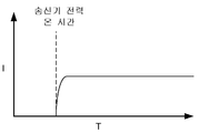
도 9a는 무선 전력 송신기의 충전 영역에 무선 전력 수신기 없는 정류기를 조사하는 관찰된 출력 임피던스이다.
[0018]
도 9B는 무선 전력 송신기의 충전 영역에 무선 전력 수신기를 갖는 정류기를 조사하는 관찰된 출력 임피던스이다.
[0019]
도 10a는 무선 전력 송신기의 충전 영역에 무선 전력 수신기 없는 송신기 전력 증폭기(PA) 입력 전류이다.
[0020]
도 10b는 무선 전력 송신기의 충전 영역에 무선 전력 수신기를 갖는 송신기 PA 입력 전류이다.
[0021]
도 11a는 무선 전력 송신기의 충전 영역에 무선 전력 수신기 없는 송신기의 PA 입력 전류 및 전압의 테스트 측정들의 트래이스이다.
[0022]
도 11b는 무선 전력 송신기의 충전 영역에 무선 전력 수신기를 갖는 송신기의 PA 입력 전류 및 전압의 테스트 측정들의 트래이스이다.
[0023]
도 12a는 무선 전력 송신기의 충전 영역에서 시뮬레이트된 로드 디바이스를 갖는 송신기의 PA 입력 전류 및 전압의 테스트 측정들의 트래이스이다.
[0024]
도 12b는 무선 전력 송신기의 충전 영역에 유효 디바이스를 갖는 송신기의 PA 입력 전류 및 전압의 테스트 측정들의 트래이스이다.
[0025]
도 13은 무선 전력 송신기의 충전 영역에의 무선 전력 수신기의 배치를 검출하기 위한 디바이스의 기능 블록도이다.
[0026]
도 14는 무선 전력 송신기의 충전 영역에의 무선 전력 수신기의 배치를 검출하기 위한 예시적인 방법의 흐름도이다.
[0027]
도 15는 도 14의 예시적인 방법의 추가의 양상들을 도시한다.
[0028]
도면들에서 예시된 다양한 특징들은 제 축척대로 그려지지 않을 수 있다. 이에 따라, 다양한 특징들의 치수들은 명확성을 위해 임의로 확장되거나 감소될 수 있다. 또한, 도면들 중 일부는 주어진 시스템, 방법 또는 디바이스의 모든 컴포넌트들을 도시하진 않을 수 있다. 마지막으로, 유사한 참조 번호들은 명세서 및 도면들에 걸쳐 유사한 특징들을 나타내는데 이용될 수 있다. [0009] FIG. 1 is a functional block diagram of an exemplary wireless power delivery system in accordance with an exemplary embodiment of the present invention.
[0010] FIG. 2 is a functional block diagram of exemplary components that may be utilized in the wireless power delivery system of FIG. 1, in accordance with various exemplary embodiments of the present invention.
[0011] FIG. 3 is a schematic diagram of a portion of the transmit or receive circuit of FIG. 2 including a transmit or receive antenna in accordance with exemplary embodiments of the invention.
[0012] FIG. 4 is a functional block diagram of a transmitter that may be used in the wireless power delivery system of FIG. 1, in accordance with exemplary embodiments of the present invention.
[0013] FIG. 5 is a functional block diagram of a receiver that may be used in the wireless power delivery system of FIG. 1, in accordance with exemplary embodiments of the present invention.
[0014] FIG. 6 is a schematic diagram of a portion of a transmit circuit that may be used in the transmit circuit of FIG. 4;
[0015] FIG. 7 is a simplified exemplary wireless charging circuit.
[0016] FIG. 8 is an equivalent DC model corresponding to the circuit of FIG.
[0017] FIG. 9A is an observed output impedance that illuminates a rectifier without a wireless power receiver in the charging region of the wireless power transmitter.
[0018] FIG. 9B is an observed output impedance that illuminates a rectifier having a wireless power receiver in the charging region of the wireless power transmitter.
[0019] FIG. 10A is a transmitter power amplifier (PA) input current without a wireless power receiver in the charging region of the wireless power transmitter.
[0020] FIG. 10B is a transmitter PA input current having a wireless power receiver in the charging region of the wireless power transmitter.
[0021] FIG. 11a is a trace of test measurements of PA input current and voltage of a transmitter without a wireless power receiver in the charging region of the wireless power transmitter.
[0022] FIG. 11 b is a trace of test measurements of the PA input current and voltage of a transmitter having a wireless power receiver in the charging region of the wireless power transmitter.
[0023] FIG. 12A is a trace of test measurements of the PA input current and voltage of a transmitter having a simulated load device in the charging region of the wireless power transmitter.
[0024] FIG. 12b is a trace of test measurements of the PA input current and voltage of the transmitter having an effective device in the charging region of the wireless power transmitter.
[0025] FIG. 13 is a functional block diagram of a device for detecting the placement of a wireless power receiver in a charging region of a wireless power transmitter.
[0026] FIG. 14 is a flow diagram of an exemplary method for detecting the placement of a wireless power receiver in a charging region of a wireless power transmitter.
[0027] FIG. 15 illustrates additional aspects of the exemplary method of FIG.
[0028] The various features illustrated in the drawings may not be drawn to scale. Accordingly, the dimensions of the various features may optionally be scaled or reduced for clarity. Moreover, some of the figures may not show all components of a given system, method or device. Finally, like reference numerals can be used to indicate similar features throughout the specification and drawings.
[0029] 첨부된 도면들과 관련하여 하기에 기술되는 상세한 설명은, 본 발명의 예시적인 실시예들의 설명으로서 의도되며 본 발명이 실시될 수 있는 실시예들만을 나타내도록 의도되는 것은 아니다. 이 설명 전반에 걸쳐 이용되는 "예시적인" 이란 용어는 "예, 보기 또는 예시로서 작용하는 것"을 의미하며, 반드시 다른 예시적인 실시예들보다 유리하거나 선호되는 것으로서 해석되어선 안 된다. 상세한 설명은 본 발명의 예시적인 실시예의 완전한 이해를 제공하기 위하여 특정 세부사항들을 포함한다. 일부 인스턴스들에서, 일부 디바이스들은 블록도 형태로 도시된다. [0029] The following detailed description, taken in conjunction with the accompanying drawings, is intended as a description of exemplary embodiments of the invention and is not intended to represent only those embodiments in which the invention may be practiced. The word "exemplary " used throughout this description means" acting as an example, instance, or illustration, "and is not necessarily to be construed as preferred or advantageous over other exemplary embodiments. The detailed description includes specific details to provide a thorough understanding of exemplary embodiments of the invention. In some instances, some devices are shown in block diagram form.
[0030] 전력을 무선으로 전달하는 것은 물리적 전기 도체의 이용 없이 송신기로부터 수신기로 전기장, 자기장, 전자기장, 또는 다른 것과 연관된 임의의 형태의 에너지를 전달하는 것을 지칭한다(예를 들어, 전력은 자유 공간을 통해 전달될 수 있음). 무선 필드(예를 들어, 자기장)로 출력된 전력은 전력 전달을 달성하기 위해 "수신 안테나"에 의해 수신되고, 캡처되거나, 또는 커플링될 수 있다. [0030] Transferring power wirelessly refers to transferring any form of energy associated with an electric field, magnetic field, electromagnetic field, or otherwise, from a transmitter to a receiver without the use of physical electrical conductors (e.g., power is passed through free space Lt; / RTI > Power output to a wireless field (e.g., a magnetic field) may be received, captured, or coupled by a "receive antenna" to achieve power delivery.
[0031]
도 1은 본 발명의 예시적인 실시예에 따라 예시적인 무선 전력 전달 시스템(100)의 기능 블록도이다. 입력 전력(102)은 에너지 전달을 제공하기 위한 필드(105)를 생성하기 위해 전력 소스(도시되지 않음)로부터 송신기(104)에 제공될 수 있다. 수신기(108)는 필드(105)에 커플링되고 출력 전력(110)에 커플링되는 디바이스(도시되지 않음)에 의한 저장 또는 소비를 위한 출력 전력(110)을 생성할 수 있다. 송신기(104) 및 수신기(108) 둘 다는 거리(112)에 의해 분리된다. 일 예시적인 실시예에서, 송신기(104) 및 수신기(108)는 상호 공진 관계(mutual resonant relationship)에 따라 구성된다. 수신기(108)의 공진 주파수 및 송신기(104)의 공진 주파수가 실질적으로 동일하거나 또는 매우 근접할 때, 송신기(104)와 수신기(108) 간의 송신 손실들이 최소화된다. 이에 따라, 무선 전력 전달은, 대형 코일들이 매우 근접(예를 들어, mm들)하게 되도록 요구할 수 있는 순수 유도성 솔루션들(purely inductive solutions)에 대조적으로 더 큰 거리에 걸쳐 제공될 수 있다. 공진 유도성 커플링 기술들은 이에 따라 다양한 유도성 코일 구성들로 그리고 다양한 거리들에 걸쳐 개선된 효율 및 전력 전달을 허용할 수 있다. [0031]
1 is a functional block diagram of an exemplary wireless
[0032]
수신기(108)는, 수신기(108)가 송신기(104)에 의해 생성되는 에너지 필드(105)에 로케이팅될 때 전력을 수신할 수 있다. 필드(105)는 송신기(104)에 의해 출력되는 에너지가 수신기(105)에 의해 캡처될 수 있는 영역에 대응한다. 일부 경우들에서, 필드(105)는 아래에서 추가로 설명되는 바와 같이, 송신기(104)의 "근거리 필드(near field)"에 대응할 수 있다. 송신기(104)는 에너지 송신을 출력하기 위해 송신 안테나(114)를 포함할 수 있다. 수신기(108)는 추가로, 에너지 송신으로부터 에너지를 수신하거나 캡처하기 위해 수신 안테나(118)를 포함한다. 근거리-필드는 송신 안테나(114)로부터 멀어지게 전력을 최소한으로 방사하는 송신 안테나(114)의 전류들 및 전하들로부터 발생하는 강한 반응 필드들(strong reactive fields)이 존재하는 영역에 대응할 수 있다. 일부 경우들에서, 근거리-필드는 대략 송신 안테나(114)의 한 파장(또는 그의 프랙션(fraction)) 내에 있는 영역에 대응할 수 있다. 송신 및 수신 안테나들(114 및 118)은 이들과 연관되는 애플리케이션들 및 디바이스들에 따라 크기조절된다. 위에서 설명된 바와 같이, 효율적인 에너지 전달은 원거리 필드(far field)로 전자기파의 에너지 대부분을 전파하기 보단, 수신 안테나(118)로 송신 안테나(114)의 필드(105)의 에너지 대부분을 커플링함으로써 발생할 수 있다. 필드(105) 내에 포지셔닝될 때, "커플링 모드"는 송신 안테나(114)와 수신 안테나(118) 간에 발현될 수 있다. 이 커플링이 발생할 수 있는 송신 및 수신 안테나들(114 및 118) 주위의 영역은 본원에서 커플링 모드 영역으로서 지칭된다. [0032]
The
[0033]
도 2는 본 발명의 다양한 예시적인 실시예들에 따라, 도 1의 무선 전력 전달 시스템(100)에서 이용될 수 있는 예시적인 컴포넌트들의 기능 블록도이다. 송신기(204)는 오실레이터(222), 구동기 회로(224) 및 필터 및 매칭 회로(226)를 포함할 수 있는 송신 회로(206)를 포함할 수 있다. 오실레이터(222)는 주파수 제어 신호(223)에 대한 응답으로 조정될 수 있는, 468.75 KHz, 6.78 MHz 또는 13.56 MHz와 같은 원하는 주파수의 신호를 생성하도록 구성될 수 있다. 오실레이터 신호는 예를 들어, 송신 안테나(214)의 공진 주파수에서 송신 안테나(214)를 구동하도록 구성되는 구동기 회로(224)에 제공될 수 있다. 구동기 회로(224)는 오실레이터(222)로부터 구형파를 수신하고 사인파를 출력하도록 구성된 스위칭 증폭기일 수 있다. 예를 들어, 구동기 회로(224)는 클래스 E 증폭기일 수 있다. 필터 및 매칭 회로(226)는 또한 고조파들 또는 다른 원치않는 주파수들을 필터링하고 송신기(204)의 임피던스를 송신 안테나(214)에 매칭시키도록 포함될 수 있다. 송신 안테나(214)를 구동하는 결과로서, 송신기(204)는 전자 디바이스를 충전 또는 가동하기에 충분한 레벨로 전력을 무선으로 출력할 수 있다. 일 예로서, 제공된 전력은 예를 들어, 상이한 전력 요건들을 갖는 상이한 디바이스들을 가동 또는 충전하도록 대략 300 밀리와트 내지 5와트 정도일 수 있다. 더 높거나 더 낮은 전력 레벨들이 또한 제공될 수 있다. [0033]
2 is a functional block diagram of exemplary components that may be utilized in the wireless
[0034]
수신기(208)는 도 2에서 도시된 바와 같은 배터리(236)를 충전하거나 또는 수신기(108)에 커플링되는 디바이스(도시되지 않음)를 가동하기 위해 AC 전력 입력으로부터 출력되는 DC 전력을 생성하도록 매칭 회로(232) 및 정류기 및 스위칭 회로(234)를 포함할 수 있는 수신 회로(210)를 포함할 수 있다. 매칭 회로(232)는 수신 회로(210)의 임피던스를 수신 안테나(218)에 매칭하도록 포함될 수 있다. 수신기(208) 및 송신기(204)는 부가적으로 별개의 통신 채널(219)(예를 들어, 블루투스, 지그비, 셀룰러 등) 상에서 통신할 수 있다. 수신기(208) 및 송신기(204)는 대안적으로 무선 필드(206)의 특성들을 이용하여 대역-내 시그널링(in-band signaling)을 통해 통신할 수 있다. [0034]
[0035]
아래에서 보다 완전히 설명되는 바와 같이, 선택적으로 디스에이블 가능 연관된 로드(예를 들어, 배터리(236))를 초기에 가질 수 있는 수신기(208)는 송신기(204)에 의해 송신되고 수신기(208)에 의해 수신된 전력의 양이 배터리(236)를 충전하기 위해 적절한지를 결정하도록 구성될 수 있다. 추가로, 수신기(208)는 전력의 양이 적절하다는 결정 시에 로드(예를 들어, 배터리(236))를 인에이블하도록 구성될 수 있다. 일부 실시예들에서, 수신기(208)는 배터리(236)의 충전 없이 무선 전력 전달 필드로부터 수신된 전력을 직접 활용하도록 구성될 수 있다. 예를 들어, 통신 디바이스, 예컨대, NFC(near-field communication) 또는 RFID(radio-frequency identification device)는 무선 전력 전달 필드와 상호작용함으로써 무선 전력 전달 필드로부터 전력을 수신 및 통신하고, 및/또는 송신기(204) 또는 다른 디바이스들과 통신하기 위해 수신된 전력을 활용하도록 구성될 수 있다. [0035]
As described more fully below,
[0036]
도 3은 본 발명의 예시적인 실시예들에 따라 송신 또는 수신 안테나(352)를 포함하는 도 2의 송신 회로(206) 또는 수신 회로(210)의 부분의 개략도이다. 도 3에서 예시된 바와 같이, 아래에서 설명된 것들을 포함하는 예시적인 실시예에서 이용되는 송신 또는 수신 회로(350)는 안테나(352)를 포함할 수 있다. 안테나(352)는 또한 "루프" 안테나(352)로서 구성되거나 또는 이로서 지칭될 수 있다. 안테나(352)는 또한 본원에서 "자기" 안테나 또는 유도 코일로서 구성되거나 또는 이로서 지칭될 수 있다. "안테나"란 용어는 일반적으로 다른 "안테나"에 커플링하기 위해 에너지를 무선으로 출력 또는 수신할 수 있는 컴포넌트를 지칭한다. 안테나는 또한, 전력을 무선으로 출력 또는 수신하도록 구성되는 타입의 코일로서 지칭될 수 있다. 본원에서 이용되는 바와 같이, 안테나(352)는 전력을 무선으로 출력 및/또는 수신하도록 구성되는 타입의 "전력 전달 컴포넌트"의 예이다. 안테나(352)는 페라이트 코어(ferrite core)(도시되지 않음)와 같은 에어(air) 코어 또는 물리적 코어를 포함하도록 구성될 수 있다. 에어 코어 루프 안테나들은 코어 부근에 배치된 관계없는 물리적 디바이스들에 대해 보다 더 용인(tolerable)될 수 있다. 또한, 에어 코어 루프 안테나(352)는 코어 영역 내의 다른 컴포넌트들의 배치를 허용한다. 또한, 에어 코어 루프는 송신 안테나(214)(도 2)의 플래인 내에 수신 안테나(218)(도 2)의 배치를 보다 쉽게 인에이블할 수 있으며, 이는 송신 안테나(214)(도 2)의 커플링된 모드 영역이 보다 강력해질 수 있다. [0036]
FIG. 3 is a schematic diagram of a portion of the transmit
[0037]
언급된 바와 같이, 송신기(104)와 수신기(108) 간의 에너지의 효율적인 전달은 송신기(104)와 수신기(108) 간에 매칭되거나 거의 매칭되는 공진 동안 발생할 수 있다. 그러나 송신기(104)와 수신기(108) 간의 공진이 매칭하지 않을 때에도, 에너지는 전달될 수 있지만, 효율은 영향을 받을 수 있다. 에너지의 전달은 송신 안테나(214)로부터 자유 공간으로 에너지를 전파하기 보단, 필드(105)가 설정되는 근처(neighborhood)에 상주하는 수신 안테나(218)에 대해 송신 안테나(214) 코일의 필드(105)로부터의 에너지를 커플링함으로써 발생한다. [0037]
Efficient transmission of energy between the
[0038]
루프 또는 자기 안테나들의 공진 주파수는 인덕턴스 및 커패시턴스에 기초한다. 인덕턴스는 단순히 안테나(352)에 의해 생성되는 인덕턴스일 수 있는 반면에, 커패시턴스는 원하는 공진 주파수에서 공진 구조를 생성하기 위해 안테나의 인덕턴스에 부가될 수 있다. 비-제한적인 예로서, 커패시터(352) 및 커패시터(354)는 공진 주파수의 신호(356)를 선택하는 공진 회로를 생성하도록 송신 또는 수신 회로(350)에 부가될 수 있다. 이에 따라, 더 큰 직경의 안테나에 대해, 공진을 유지하기 위해 필요한 커패시턴스의 크기는 루프의 직경 또는 인덕턴스가 증가함에 따라 감소할 수 있다. 또한, 안테나의 직경이 증가함에 따라, 근거리 필드의 효율적인 에너지 전달 영역이 증가할 수 있다. 다른 컴포넌트들을 이용하여 형성되는 다른 공진 회로들이 또한 가능하다. 다른 비-제한적인 예로서, 커패시터는 안테나(350)의 2개의 단자들 사이에서 병렬로 배치될 수 있다. 송신 안테나에 대해, 안테나(352)의 공진 주파수에 실질적으로 대응하는 주파수를 갖는 신호(358)가 안테나(352)에 대한 입력일 수 있다. [0038]
The resonant frequencies of the loop or magnetic antennas are based on inductance and capacitance. The inductance may simply be the inductance produced by the
[0039]
일 실시예에서, 송신기(104)는 송신 안테나(114)의 공진 주파수에 대응하는 주파수를 갖는 시변 자기장(time varying magnetic field)을 출력하도록 구성될 수 있다. 수신기가 필드(105) 내에 있을 때, 시변 자기장은 수신 안테나(118)에서 전류를 유도할 수 있다. 위에서 설명된 바와 같이, 수신 안테나(118)가 송신 안테나(118)의 주파수로 공진하도록 구성되는 경우, 에너지가 효율적으로 전달될 수 있다. 수신 안테나(118)에서 유도된 AC 신호는 로드를 가동하거나 충전하도록 제공될 수 있는 DC 신호를 생성하기 위해 위에서 설명된 바와 같이 정류될 수 있다. [0039]
In one embodiment, the
[0040]
도 4는 본 발명의 예시적인 실시예들에 따라, 도 1의 무선 전력 전달 시스템에서 이용될 수 있는 송신기(404)의 기능 블록도이다. 송신기(404)는 송신 회로(406) 및 송신 안테나(414)를 포함할 수 있다. 송신 안테나(414)는 도 3에서 도시된 바와 같은 안테나(352)일 수 있다. 송신 회로(406)는 송신 안테나(414) 근처에 에너지(예를 들어, 자속(magnetic flux))의 생성을 발생시키는 오실레이팅 신호를 제공함으로써 송신 안테나(414)에 RF 전력을 제공할 수 있다. 송신기(404)는 임의의 적합한 주파수에서 동작할 수 있다. 예로서, 송신기(404)는 6.78 MHz ISM 대역에서 동작할 수 있다. [0040]
4 is a functional block diagram of a
[0041]
송신 회로(406)는 송신 안테나(414)에 대해 송신 회로(406)의 임피던스(예를 들어, 50옴)를 매칭하기 위한 고정 임피던스 매칭 회로(409) 및 수신기들(108)(도 1)에 커플링되는 디바이스들의 자체 전파방해(self jamming)를 방지하기 위한 레벨로 고조파 방출들을 감소시키도록 구성되는 저역 통과 필터(LPF)(408)를 포함할 수 있다. 다른 예시적인 실시예들은 다른 주파수들을 통과시키면서 특정 주파수들을 감쇄시키는 노치 필터들을 포함(그러나 이것으로 제한되지 않음)하는 상이한 필터 토폴로지들을 포함할 수 있고 구동기 회로(424)에 의해 드로우되는 DC 전류 또는 안테나(414)에 대한 출력 전력과 같이 측정 가능한 송신 메트릭들에 기초하여 변동될 수 있는 적응형 임피던스 매칭을 포함할 수 있다. 송신 회로(406)는 추가로 오실레이터(423)에 의해 결정된 바와 같이 RF 신호를 구동하도록 구성되는 구동기 회로(424)를 더 포함한다. 송신 회로(406)는 이산 디바이스들 또는 회로들로 구성될 수 있거나, 또는 대안적으로, 통합된 어셈블리로 구성될 수 있다. 송신 안테나(414)로부터 출력된 예시적인 RF 전력은 대략 2.5와트 정도일 수 있다. [0041]
The transmitting
[0042]
송신 회로(406)는 추가로, 특정 수신기들에 대해 송신 국면들(또는 듀티 사이클들) 동안 오실레이터(423)를 선택적으로 인에이블하기 위해, 오실레이터(423)의 주파수 또는 위상을 조정하기 위해 그리고 그의 부착된 수신기들을 통해 이웃 디바이스들과 상호작용하도록 통신 프로토콜을 구현하기 위해 출력 전력 레벨 조정하기 위한 제어기(415)를 포함할 수 있다. 제어기(415)는 본원에서 프로세서(415)로서 또한 지칭될 수 있다는 것에 주의한다. 송신 경로에서 오실레이터 위상 및 관련된 회로의 조정은, 특히 하나의 주파수로부터 다른 주파수로 천이할 때 대역외 방출들의 감소를 허용할 수 있다. [0042]
The transmit
[0043]
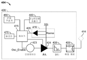
송신 회로(406)는 추가로 송신 안테나(414)에 의해 생성된 근거리 필드 부근에서 활성 수신기들의 존재 또는 부재를 검출하기 위한 로드 감지 회로(416)를 포함할 수 있다. 예로서, 로드 감지 회로(416)는, 아래에서 추가로 설명되는 바와 같이 송신 안테나(414)에 의해 생성되는 필드 부근에 활성 수신기들의 존재 또는 부재에 의해 영향을 받을 수 있는, 구동기 회로(424)로 흐르는 전류를 모니터링한다. 구동기 회로(424) 상의 로딩에 대한 변화들의 검출은 에너지를 송신하기 위해 오실레이터(423)를 인에이블할지 그리고 활성 수신기와 통신할지를 결정하는데 있어 이용하도록 제어기(415)에 의해 모니터링된다. 아래에서 보다 완전히 설명되는 바와 같이, 구동기 회로(424)에서 측정되는 전류는, 비유효(invalid) 디바이스가 송신기(404)의 무선 전력 전달 영역 내에 포지셔닝되는지를 결정하는데 이용될 수 있다. [0043]
The transmit
[0044]
송신 안테나(414)는 저항 손실들을 낮게 유지하도록 선택된 두께, 폭 및 금속 타입을 갖는 안테나 스트립으로서 또는 리츠 와이어(Litz wire)로 구현될 수 있다. 일 구현에서, 송신 안테나(414)는 일반적으로 테이블, 매트(mat), 램프(lamp) 또는 다른 덜 휴대 가능 구성과 같은 더 큰 구조와의 연관을 위해 구성될 수 있다. 이에 따라, 송신 안테나(414)는 일반적으로, 실제 치수가 되기 위해 "턴(turn)들"을 요구하지 않을 수 있다. 송신 안테나(414)의 예시적인 구현은 "전기적으로 소형(electrically small)"(즉, 파장의 프랙션)이고 공진 주파수를 정의하도록 커패시터들을 이용함으로써 더 낮은 유용한 주파수들에서 공진하도록 튜닝될 수 있다. [0044]
The transmit
[0045]
송신기(404)는 송신기(404)와 연관될 수 있는 수신기 디바이스들의 상태 및 소재들에 관한 정보를 수집 및 트래킹할 수 있다. 따라서, 송신 회로(406)는 제어기(415)(본원에서 프로세서로서 또한 지칭됨)에 연결되는 존재 검출기(480), 인클로징된 검출기(460) 또는 이들의 결합을 포함할 수 있다. 제어기(415)는 존재 검출기(480) 및 인클로징된 검출기(460)로부터의 존재 신호들에 대한 응답으로 구동기 회로(424)에 의해 전달되는 전력의 양을 조정할 수 있다. 송신기(404)는, 다수의 전력 소스들을 통해 예를 들어, 예컨대, 빌딩에 존재하는 종래의 AC 전력을 변환하기 위한 AC-DC 변환기(도시되지 않음), 종래의 DC 전력 소스를 송신기(404)에 적합한 전압으로 변환하기 위한 DC-DC 변환기(도시되지 않음), 또는 종래의 DC 전력 소스(도시되지 않음)로부터 직접적으로 전력을 수신할 수 있다. [0045]
[0046]
비-제한적인 예로서, 존재 검출기(480)는 송신기(404)의 커버리지 영역에 삽입되는, 충전될 디바이스의 초기 존재를 감지하도록 활용되는 모션 검출기일 수 있다. 검출 후에, 송신기(404)는 턴 온될 수 있고 디바이스에 의해 수신된 RF 전력은 미리 결정된 방식으로 Rx 디바이스 상의 스위치를 토글링하는데 사용될 수 있으며, 이는 결국 송신기(404)의 구동 지점 임피던스로의 변화들을 초래한다. [0046]
As a non-limiting example, the
[0047]
다른 비-제한적인 예로서, 존재 검출기(480)는 예를 들어, 적외선 검출, 모션 검출, 또는 다른 적합한 수단에 의해 인간을 검출 가능한 검출기일 수 있다. 일부 예시적인 실시예들에서, 송신 안테나(414)가 특정 주파수에서 송신할 수 있는 전력의 양을 제한하는 규제들이 있을 수 있다. 일부 경우들에서, 이들 규제들은 전자기 방사로부터 인간들을 보호하도록 의도된다. 그러나 송신 안테나(414)가 예를 들어, 차고들, 작업 현장들, 가게들 등과 같이 인간들에 의해 빈번하게 점유되거나 인간들에 의해 점유되지 않는 영역들에 배치되는 환경들이 있을 수 있다. 이들 환경들에 인간들이 없는 경우, 보통의 전력 제한 규제들 위로 송신 안테나(414)의 전력 출력을 증가시키는 것이 허용 가능할 수 있다. 즉, 제어기(415)는, 인간 존재에 대한 응답으로 규제 레벨 또는 그 미만으로 송신 안테나(414)의 전력 출력을 조정하고, 인간이 송신 안테나(414)의 전자기 필드로부터 규제 거리 외부에 있을 때 규제 레벨 위의 레벨로 송신 안테나(414)의 전력 출력을 조정할 수 있다. [0047]
As another non-limiting example, the
[0048] 비-제한적인 예로서, 인클로징된 검출기(460)(본원에서 인클로징된 대응 검출기 또는 인클로징된 공간 검출기로서 또한 지칭될 수 있음)는 인클로저가 폐쇄 또는 개방 상태에 있을 때를 결정하기 위한 감지 스위치와 같은 디바이스일 수 있다. 송신기가 인클로징된 상태에 있는 인클로저에 있을 때, 송신기의 전력 레벨은 증가될 수 있다. [0048] As a non-limiting example, an enclosed detector 460 (which may also be referred to herein as a corresponding detector enclosed or an enclosed space detector) may be configured to detect when the enclosure is in the closed or open state A device such as a switch. When the transmitter is in an enclosure in an enclosed state, the power level of the transmitter can be increased.
[0049]
본 개시의 하나 또는 그 초과의 양상들에 따라, 로드 감지 회로(416)는, 수신기가 송신기(404)의 충전 영역에 배치되는 것에 대한 응답으로, 송신기(404) 및 수신기(예를 들어, 도 5의 수신기(508))의 송신 및 수신 코일들 간에 각각 적용되거나 변경되는 필드로부터 발생하는 동적 임피던스 변화를 검출하도록 구성된 회로를 포함할 수 있다. 일 구현에서, 로드 감지 회로(416)는 송신기에 대해 제시되는 임피던스의 변화를 검출하도록 구성된 회로를 포함할 수 있으며, 이 변화는 수신기가 충전 영역에 배치되는 것에 대한 응답으로, 송신 및 수신 코일들 간에서 변경되거나 충전 영역에 적용되는 필드로부터 발생한다. 관련된 양상들에서, 로드 감지 회로(416)는 시간 인터벌 내의 임피던스 응답의 타입 및/또는 시간 인터벌 내의 임피던스 변화 패턴(반복 파형 또는 형상을 반드시 포함할 필요는 없음)을 검출할 수 있다. 예를 들어, 동적 임피던스 변화는 필드의 초기 적용 동안 수신기의 커패시터(예를 들어, 필터 커패시터)의 충전과 연관되는 특성 파형을 인지함으로써 지각된다. 추가 관련된 양상들에서, 특성 파형은 출력 임피던스, 송신기 전류 및/또는 송신기 전압에 기초하거나 관련될 수 있다. 예를 들어, 특성 파형은 수신기에 대한 송신기 전류에서 일시적인 스파이크(transient spike)를 포함할 수 있다. 로드 감지 회로(416)는 수신기가 충전 영역에 있게 되는 것에 대한 응답으로, 전력-절감 모드로부터 최대-충전 모드로 송신기(404)를 스위칭하도록 제어기(415)와 함께 동작할 수 있다. [0049]
In accordance with one or more aspects of the present disclosure, the
[0050]
관련된 양상들에서, 로드 감지 회로(416) 등은 예시되거나 그렇지 않은 송신기(404)의 하나 또는 그 초과의 컴포넌트들과 함께 동작할 수 있다. 추가의 관련된 양상들에서, 로드 감지 회로(416) 등은 도 7a 내지 도 13을 참조하여 아래에서 추가로 상세히 설명되는 특징들에 따라 송신기(404)의 충전 영역에의 수신기의 배치를 검출하도록 구성될 수 있다. [0050]
In related aspects, the
[0051]
예시적인 실시예에서, 송신기(404)가 무기한으로 온(on) 상태를 유지하지 않는 방법이 이용될 수 있다. 이 경우에, 송신기(404)는 사용자-결정 시간량 이후 차단(shut-off)되도록 프로그래밍될 수 있다. 이 특징은 송신기(404), 특히 구동기 회로(424)가, 그 주변의 무선 디바이스들이 완전히 충전된 이후 오랫동안 실행되는 것을 방지한다. 이 이벤트는 디바이스가 완전히 충전되었고 리피터 또는 수신 안테나(218) 중 어느 하나로부터 송신된 신호를 검출하기 위한 회로의 장애에 기인할 수 있다. 다른 디바이스가 그의 주변에 배치된 경우 송신기(404)가 자동으로 셧 다운되는 것을 방지하기 위해, 송신기(404) 자동 차단 특징은 그 주변에 검출된 모션의 결여의 세팅된 기간 이후에만 활성화될 수 있다. 사용자는 비활성 시간 인터벌을 결정하고 그것을 요구에 따라 변화시킬 수 있을 수도 있다. 비-제한적인 예로서, 시간 인터벌은, 디바이스가 초기에 완전히 방전되었다는 가정하에 특정 타입의 무선 디바이스를 완전히 충전하는데 필요한 것보다 길어질 수 있다. [0051]
In an exemplary embodiment, a method may be used in which the
[0052]
도 5는 본 발명의 예시적인 실시예들에 따라, 도 1의 무선 전력 전달 시스템에서 이용될 수 있는 수신기(508)의 기능 블록도이다. 수신기(508)는 수신 안테나(518)를 포함할 수 있는 수신 회로(510)를 포함한다. 수신기(508)는 추가로 수신된 전력을 제공하기 위해 디바이스(550)에 커플링된다. 수신기(508)는 디바이스(550) 외부에 있는 것으로서 예시되지만, 디바이스(550)에 통합될 수 있다는 것이 주의되어야 한다. 에너지는 수신 안테나(518)에 의해 무선으로 전파되고, 그 후 수신 회로(510)의 잔여부를 통해 디바이스(550)에 커플링될 수 있다. 예로서, 충전 디바이스는 모바일 폰들, 휴대용 음악 재생기들, 랩톱 컴퓨터들, 태블릿 컴퓨터들, 컴퓨터 주변 디바이스들, 통신 디바이스들(예를 들어, 블루투스 디바이스들), 디지털 카메라들, 보청기들(또는 다른 의료 디바이스들) 등과 같은 디바이스들을 포함할 수 있다. [0052]
5 is a functional block diagram of a
[0053]
수신 안테나(518)는 송신 안테나(414)(도 4)와 동일한 주파수 또는 특정 범위의 주파수들 내에서 공진하도록 튜닝될 수 있다. 수신 안테나들(518)은 송신 안테나(414)와 유사하게 치수가 정해질 수 있거나, 또는 연관된 디바이스(550)의 치수들에 기초하여 상이하게 크기조절될 수 있다. 예로서, 디바이스(550)는 송신 안테나(414)의 직경 또는 길이보다 더 작은 직경 또는 길이 치수를 갖는 휴대용 전자 디바이스일 수 있다. 이러한 예에서, 수신 안테나(518)는 튜닝 커패시터(도시되지 않음)의 커패시턴스 값을 감소시키고 수신 코일의 임피던스를 증가시키기 위해 다중 턴 코일로서 구현될 수 있다. 예로서, 수신 안테나(518)는 수신 안테나(518)의 루프 턴들(즉, 와인딩(windings))의 수 및 인터-와인딩 커패시턴스(inter-winding capacitance)를 감소시키고 안테나 직경을 최대화하기 위해 디바이스(550)의 실질적인 둘레 주위에 배치될 수 있다. [0053]
The receive
[0054]
수신 회로(510)는 수신 안테나(518)에 대한 임피던스 매칭을 제공할 수 있다. 수신 회로(510)는 디바이스(550)에 의한 이용을 위해 충전 전력으로 수신된 RF 에너지 소스를 변환하기 위한 전력 변환 회로(506)를 포함한다. 전력 변환 회로(506)는 RF-투-DC 변환기(520)를 포함하고 DC-투-DC 변환기(522)를 또한 포함할 수 있다. RF-투-DC 변환기(520)는 수신 안테나(518)에서 수신된 RF 에너지 신호를, Vrect에 의해 표현되는 출력 전압을 갖는 비-교류 전력으로 정류한다. DC-투-DC 변환기(522)(또는 다른 전력 레귤레이터)는 Vout 및 Iout에 의해 표현되는 출력 전압 및 출력 전류를 갖는, 디바이스(550)와 호환 가능한 전기 전위(예를 들어, 전압)로 정류된 RF 에너지 신호를 변환한다. 부분적 및 완전 정류기들, 레귤레이터들, 브리지들, 더블러(doubler)들은 물론, 선형 및 스위칭 변환기들을 포함하는 다양한 RF-투-DC 변환기들이 고려된다. [0054] The receiving
[0055]
수신 회로(510)는 추가로, 수신 안테나(518)를 전력 변환 회로(506)에 연결하기 위해 또는 대안적으로 전력 변환 회로(506)와 연결해제하기 위해 스위칭 회로(512)를 포함할 수 있다. 수신 안테나(518)를 전력 변환 회로(506)로부터 연결해제하는 것은 디바이스(550)의 충전을 정지시킬 뿐만 아니라 송신기(404)(도 2)에 의해 "지각"되는 바와 같은 "로드"를 변화시킨다. [0055]
The receiving
[0056]
위에서 개시된 바와 같이, 송신기(404)는 송신기 구동기 회로(424)에 제공되는 바이어스 전류의 등락들을 검출할 수 있는 로드 감지 회로(416)를 포함한다. 이에 따라, 송신기(404)는, 수신기들이 송신기의 근거리 필드에 존재할 때를 결정하기 위한 매커니즘을 갖는다. [0056]
As described above, the
[0057]
다수의 수신기들(508)이 송신기의 근거리 필드에 존재할 때, 다른 수신기들이 송신기에 보다 효율적으로 커플링하는 것을 가능케 하도록 하나 또는 그 초과의 수신기들의 로딩 및 언로딩을 시간 멀티플렉싱하는 것이 바람직할 수 있다. 수신기(508)는 또한 근처 송신기들 상의 로딩을 감소시키도록 또는 다른 근처 수신기들에 대한 커플링을 제거하도록 클로킹(cloak)될 수 있다. 수신기의 이러한 "언로딩(unloading)"은 또한 본원에서 "클로킹"으로서 알려진다. 또한, 송신기(404)에 의해 검출되고 수신기(508)에 의해 제어되는 언로딩과 로딩 간의 이러한 스위칭은 아래에서 보다 완전히 설명되는 바와 같이 수신기(508)로부터 송신기(404)로의 통신 매커니즘을 제공할 수 있다. 또한, 프로토콜은 수신기(508)로부터 송신기(404)로의 메시지의 송신을 가능케 하는 스위칭과 연관될 수 있다. 예로서, 스위칭 속도는 대략 100μsec정도일 수 있다. [0057]
It may be desirable to time multiplex the loading and unloading of one or more receivers to enable other receivers to more efficiently couple to the transmitter when
[0058]
예시적인 실시예에서, 송신기(404)와 수신기(508) 간의 통신은 종래의 양방향 통신(즉, 커플링 필드를 이용한 대역내 시그널링)보단, 디바이스 감지 및 충전 제어 매커니즘을 지칭한다. 즉, 송신기(404)는 에너지가 근거리 필드에서 이용 가능한지를 조정하도록 송신된 신호의 온/오프 키잉(on/off keying)을 이용할 수 있다. 수신기는 송신기(404)로부터의 메시지로서 에너지의 이러한 변화들을 해석할 수 있다. 수신기 측에서, 수신기(508)는 얼마나 많은 전력이 필드로부터 수용되는지를 조정하도록 수신 안테나(518)의 튜닝 및 디-튜닝(de-tuning)을 이용할 수 있다. 일부 경우들에서, 튜닝 및 디-튜닝은 스위칭 회로(512)를 통해 달성될 수 있다. 송신기(404)는 필드로부터 이용된 전력의 이러한 차이를 검출하고 수신기(508)로부터의 메시지로서 이러한 변화들을 해석할 수 있다. 송신 전력 및 로드 거동의 다른 형태의 변조가 활용될 수 있다는 것이 주의된다. [0058]
In the exemplary embodiment, the communication between the
[0059]
수신 회로(510)는 송신기로부터 수신기로의 정보 시그널링에 대응할 수 있는 수신된 에너지 등락들을 식별하는데 이용되는 시그널링 검출기 및 비콘 회로(514)를 더 포함할 수 있다. 또한, 시그널링 및 비콘 회로(514)는 또한, 감소된 RF 신호 에너지(즉, 비콘 신호)의 송신을 검출하고 무선 충전을 위한 수신 회로(510)를 구성하기 위해 수신 회로(510) 내의 가동-중단(un-powered) 또는 전력-고갈 회로들을 어웨이크(awake)하기 위해 공칭 전력으로 감소된 RF 신호 에너지를 정류하는데 이용될 수 있다. [0059]
Receiving
[0060]
수신 회로(510)는 추가로, 본원에서 설명되는 스위칭 회로(512)의 제어를 비롯해서 본원에서 설명되는 수신기(508)의 프로세스들을 조절하기 위한 프로세서(516)를 포함한다. 수신기(508)의 클로킹은 또한 충전 전력을 디바이스(550)에 제공하는 외부 유선 충전 소스(예를 들어, 벽/USB 전력)의 검출을 포함하는 다른 이벤트들의 발생 시에 발생할 수 있다. 수신기의 클로킹의 제어 외에도, 프로세서(516)는 또한, 비콘 상태를 결정하고 송신기(404)로부터 전송된 메시지를 추출하도록 비콘 회로(514)를 모니터링할 수 있다. 프로세서(516)는 또한 개선된 성능을 위해 DC-투-DC 변환기(522)를 조정할 수 있다. [0060]
Receiving
[0061]
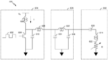
도 6은 도 4의 송신 회로(406)에서 이용될 수 있는 송신 회로(600)의 부분의 개략도이다. 송신 회로(600)는 도 4의 위에서 설명된 바와 같은 구동기 회로(624)를 포함할 수 있다. 위에서 설명된 바와 같이, 구동기 회로(624)는 구형파를 수신하고 송신 회로(650)에 제공될 사인파를 출력하도록 구성될 수 있는 스위칭 증폭기일 수 있다. 일부 경우들에서, 구동기 회로(624)는 증폭기 회로로서 지칭될 수 있다. 구동기 회로(624)는 클래스 E 증폭기로서 도시되지만, 임의의 적합한 구동기 회로(624)가 본 발명의 실시예들에 따라 이용될 수 있다. 구동기 회로(624)는 도 4에서 도시된 바와 같은 오실레이터(423)로부터의 입력 신호(602)에 의해 구동될 수 있다. 구동기 회로(624)에는 또한 송신 회로(650)를 통해 전달될 수 있는 최대 전력을 제어하도록 구성되는 구동 전압(VD)이 제공될 수 있다. 고조파들을 제거 또는 감소시키기 위해, 송신 회로(600)는 필터 회로(626)를 포함할 수 있다. 필터 회로(626)는 3폴(커패시터(634), 인덕터(632) 및 커패시터(636)) 저역 통과 필터 회로(626)일 수 있다. [0061]
6 is a schematic diagram of a portion of a transmit
[0062]
필터 회로(626)에 의해 출력된 신호는 안테나(614)를 포함하는 송신 회로(650)에 제공될 수 있다. 송신 회로(650)는 구동기 회로(624)에 의해 제공되는 필터링된 신호의 주파수에서 공진할 수 있는 (예를 들어, 안테나의 인덕턴스 또는 커패시턴스 또는 부가적인 커패시터 컴포넌트에 기인할 수 있는) 인덕턴스 및 커패시턴스(620)를 갖는 직렬 공진 회로를 포함할 수 있다. 송신 회로(650)의 로드는 가변 레지스터(622)에 의해 표현될 수 있다. 로드는 송신 회로(650)로부터 전력을 수신하도록 포지셔닝되는 무선 전력 수신기(508)의 함수일 수 있다. [0062]
The signal output by the
[0063] 본 개시에 있어서, 예를 들어, 충전 패드와 같은 무선 전력 송신기의 충전 영역에서 전력 수신기(들)의 검출의 하기의 양상들을 개선하는 것이 바람직하다. 무선 전력 시스템에 있어서, 충전 패드의 충전 영역에 배치된 디바이스를 검출하는 것이 바람직하다. 일부 무선 충전기들은 충전 패드 상에 어떠한 디바이스들도 없을 때 더 낮은 전력 상태가 된다. 이는 대기 전력 소산을 감소시키며, 이는 결국 예를 들어, 몇 일 동안과 같이 전체 효율을 증가시킨다. [0063] In the present disclosure, it is desirable to improve the following aspects of the detection of the power receiver (s) in the charging region of a wireless power transmitter, for example, a charging pad. In a wireless power system, it is desirable to detect a device disposed in the charging area of the charging pad. Some wireless chargers are in a lower power state when there are no devices on the charging pad. This reduces standby power dissipation, which ultimately increases the overall efficiency, e.g., for several days.
[0064] 그러나 충전기 패드가 이러한 더 낮은 전력 상태에 있을 때, 디바이스들이 충전 영역에 배치되는 것을 검출하는 것이 보다 어려워질 수 있는데, 그 이유는 RF 에너지가 대부분의 시간 동안 없거나, 충전기 패드가 턴 온되어 있을 때보다 훨씬 더 낮은 레벨에 있을 수 있기 때문이다. 이는 사용자가 패드 상에 디바이스를 배치하고 충전기 패드를 다시 턴 온하지 않았거나 다시 턴 온되는데 오랜 시간이 걸린다는 것을 의미한다. 이는 충전의 지연 및 열등한 사용자 경험을 초래할 수 있다. [0064] However, when the charger pad is in this lower power state, it can be more difficult to detect that the devices are placed in the charging area, because when RF energy is not present for most of the time, or when the charger pad is turned on Because it can be at a much lower level. This means that it takes a long time for the user to place the device on the pad and not turn the charger pad back on or turn it back on again. This can lead to delays in charging and poor user experience.
[0065] 이것을 극복하는 하나의 방식은 디바이스가 충전 영역에 배치됨으로써 충전기의 RF 필드 상에 있게 되는 로드를 측정함으로써 이루어진다. 충전기가 충전 필드(심지어 약하거나 간헐적인 필드임)를 생성할 때, 그 필드 내의 객체는 관찰되는 임피던스에서의 변화를 유발한다. 충전기가 특정 제한에 걸쳐 임피던스의 변화를 검출하는 경우, 충전기는 턴 온되고 로드를 가동할 수 있다. 본원에서 이용되는 바와 같이, 임피던스는 실제 임피던스(저항) 및/또는 가상 임피던스(리액턴스(reactance)) 둘 다를 지칭할 수 있다. 시스템은 디바이스가 충전 영역에 배치될 때 가동을 위해 임피던스의 어느 한 타입의 변화를 검출 또는 관찰하도록 구성될 수 있다. [0065] One way to overcome this is by measuring the load on the RF field of the charger by placing the device in the charging area. When the charger generates a charge field (even a weak or intermittent field), the object in that field causes a change in the observed impedance. If the charger detects a change in impedance over a certain limit, the charger can be turned on and the load activated. As used herein, an impedance may refer to both an actual impedance (resistance) and / or a virtual impedance (reactance). The system may be configured to detect or observe a change in either type of impedance for operation when the device is placed in the charging area.
[0066] 위에서 설명된 접근법이 다수의 경우들에서 작동할 수 있지만, 이슈들이 발생할 수 있는 상황들이 존재한다. 예를 들어, 큰 충전 패드 상에 배치되는 작은 디바이스는 충전 패드가 충전을 시작하도록 시그널링하거나 트리거하기 위한 임피던스 변화를 충분히 생성하지 않을 수 있다. 다른 예에서, 충전 패드(또는 수신 디바이스)의 특정 설계들은 특히, 효율을 개선하기 위해 임피던스 변화를 최소화하도록 의도될 수 있다. 또 다른 예에서, 충전기 패드 상의 이물질들(예를 들어, 동전, 열쇠 등)은 리액턴스 시프트를 야기할 수 있으며, 이는 시스템이 충전 영역 내의 디바이스 없이도 충전을 시작하게 할 수 있다. [0066] While the approach described above can work in many cases, there are situations in which issues can arise. For example, a small device placed on a large fill pad may not generate enough impedance changes to signal or trigger the fill pad to begin charging. In another example, the specific designs of the charging pad (or receiving device) may be specifically designed to minimize the impedance variation to improve efficiency. In another example, foreign objects (e.g., coins, keys, etc.) on the charger pad may cause a reactance shift, which may cause the system to begin charging without devices in the charging area.
[0067] 충전 패드 등 상에/근처에 전력 수신 디바이스들을 검출하기 위한 기존의 접근법들에 관한 이슈들을 극복하기 위해, 본 개시는 아래의 개선들을 설명한다. 본 개시에서, 아래에서 이어지는 설명된 방법들 및 접근법들은 단독으로 또는 임의로 결합하여 이용될 수 있다. [0067] In order to overcome the issues related to existing approaches for detecting power receiving devices on / near a charging pad or the like, this disclosure describes the following improvements. In the present disclosure, the described methods and approaches described below may be used alone or in any combination.
[0068] 본 개시의 일 양상에 따라, 전력 수신 디바이스를 검출하기 위해 전력 수신 디바이스의 정상 상태 임피던스와 상이한 파라미터를 측정하는 것을 포함하는 기술이 제공된다. 무선 전력 수신기들은 수신된 RF 에너지를 유용한 DC 전력으로 다시 변환하기 위한 정류 및 필터링을 포함한다. 이는, 초기 전력-가동 시에, 필터 커패시터가 정상 상태 동작 동안 검출되었을 수 있는 훨씬 더 낮은 임피던스를 제시할 수 있다는 것을 의미한다. 이 일시적으로 더 낮은 임피던스의 효과는, 예를 들어, 디바이스가 충전 패드 상에 배치되는지를 결정하도록 검출 및 이용될 수 있다. 예를 들어, 정상 상태 동작에 비해, 초기 전력-가동 시에 전력 수신 디바이스의 필터 커패시터의 훨씬 더 낮은 임피던스는 일시적(transient) 또는 단기 임피던스 변화의 형태로 측정 가능하거나 검출 가능한 효과를 발생시킬 수 있다. [0068] According to an aspect of the present disclosure, a technique is provided that includes measuring a parameter that is different from the steady state impedance of the power receiving device to detect the power receiving device. The wireless power receivers include rectification and filtering to convert the received RF energy back to useful DC power. This means that at initial power-up, the filter capacitor can present a much lower impedance that may have been detected during steady-state operation. This temporarily lower effect of the impedance can be detected and used, for example, to determine if the device is placed on the charging pad. For example, compared to steady-state operation, a much lower impedance of the filter capacitor of the power receiving device at initial power-up can produce measurable or detectable effects in the form of transient or short-term impedance changes .
[0069] 이 접근법에 대해 몇 개의 이점들이 존재한다. 첫째로, 언로딩된 패드가 송신기에 대해 개회로로서 나타나기 때문에, 미충전 커패시터에 의해 제시되는 근접 쇼트 회로(near short circuit)는 훨씬 더 큰 임피던스 변화를 초래할 것이어서, 그것이 검출되기 더 쉽게 된다. 둘째로, 이물질들(예를 들어, 동전들)이 일반적으로 정류기들 또는 커패시터들을 포함하지 않을 것이므로, 단기 임피던스 변화는 충전 패드 상의 새로운 객체가 사실상 전력 수신기이며 동전 등이 아니라는 것을 검증하기 위한 효과적인 방식이다. 다수의 이물질들은 금속을 포함하고, 임피던스 변화를 유발할 것이다. 셋째로, 단기 임피던스 변화를 검출하기 위한 접근법은 수신기 측 상의 특수한 또는 부가적인 하드웨어를 요구하지 않는다. [0069] There are several advantages to this approach. First, because the unloaded pad appears as an open circuit to the transmitter, the near short circuit presented by the uncharged capacitor will result in a much larger impedance change, which makes it easier to detect. Second, because the foreign objects (e.g., coins) will generally not include rectifiers or capacitors, the short-term impedance change is an effective way to verify that the new object on the charging pad is in fact a power receiver and not a coin, to be. Many foreign substances will contain metal and will cause impedance changes. Third, the approach to detecting short-term impedance changes does not require special or additional hardware on the receiver side.
[0070]
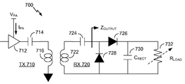
도 7은 송신기(710)가 좌측 상에 있고 수신기(720)가 우측 상에 있는 예시적인 무선 전력 시스템(700)의 단순화된 개략도를 제공한다. 송신기(710)는, 결국 인덕터(716)(도 6의 송신 회로(650)의 인덕터(614)에 대응함)에 커플링되는 커패시터(714)(도 6의 송신 회로(650)의 커패시터(620)에 대응함)에 커플링되는 송신 전력 증폭기(PA)(712)(도 6의 구동기 회로(624)의 스위칭 증폭기에 대응함)를 포함하며, 커패시터(714) 및 인덕터(716)는 집합적으로 도 6의 구동기 회로(624)에 의해 제공되는 필터링된 신호의 주파수에서 공진할 수 있는 인덕터(614) 및 커패시턴스(620)를 갖는 직렬 공진 회로에 대응하거나 이로서 기능할 수 있다. 송신기(710)의 커패시터(714) 및 인덕터(716)는, 인덕터(716)가 수신기(720)에 무선 전력을 커플링하기 위한 자기장을 생성하는데 이용되는 코일로 형성될 수 있는 공진 회로를 형성한다. [0070]
Figure 7 provides a simplified schematic diagram of an exemplary
[0071]
수신기(720)는, 커패시터(724)(도 3의 커패시터(354) 또는 커패시터(356)에 대응함)에 커플링되는 인덕터(722)(코일로 형성되고 인덕터(716)에 커플링되고 이로부터 무선 전력을 수신할 수 있고 도 5의 수신기(500)의 안테나(518)에 대응할 수 있음)를 포함하며, 인덕터(722) 및 커패시터(724)는 수신기(720)에서 공진 회로를 형성하고 공진 회로의 공진 주파수를 결정한다. 공진 주파수는 결국 정류기의 다이오드들(726, 728)에 커플링된다. 다이오드(728)의 캐소드 및 다이오드(728)의 애노드는 커패시터(CRECT)(730)에 커플링된다. 다이오드들(726, 728) 및 커패시터(CRECT)(730)는 RF-투-DC 변환기(도 5의 전력 변환 회로(506)의 RF-투-DC 변환기(520)에 대응함)를 형성하거나 그 부분일 수 있다. 커패시터(CRECT)(730)는 결국 RLOAD(732)와 병렬로 커플링될 수 있다. ZOUTPUT는 정류기를 조사하는 PA(712)에 의해 검출되는 출력 임피던스에 대응한다. [0071] The
[0072]
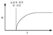
도 8은 무선 충전 회로(800)의 훨씬 더 단순화된 표현을 도시하며, 여기서 송신 및 수신 공진기들의 커플링 및 손실들은 저항들(RTX(810) 및 RRX(820))로서 도시된다. 수신기에서, 다이오드(830)는 커패시터(CRECT)(730)에 커플링된다. 잔여 회로 컴포넌트들은 도 7을 참조하여 위에서 설명된 것들과 유사하다. 저항들 및 커패시터의 결합은 예측 가능한 시상수를 갖는 RC 네트워크를 형성할 수 있다는 것에 주의한다. 좌측 상의 증폭기로부터 이 RC 네트워크를 조사할 때, 관찰된 임피던스는 낮은 상태(low)로 시작하고 그 후 커패시터가 충전을 시작함에 따라 상승할 것이다. [0072] Figure 8 illustrates a much simpler representation of a
[0073] 낮은 상태로 시작하고 그 후 상승하는 관찰된 임피던스의 광경은 도 9a에서 도시된다. PA가 우선 텅빈 패드의 경우에 턴 온할 때, 보통 PA는 머지않아 동일한 임피던스를 지각한다. 저항은 변하지 않는 특정 값으로 감지된다. 패드 상의 이물질의 경우에, 감지된 저항은 상이하지만 변하지 않거나 일정한 채로 유지된다. 복합 임피던스는 저항 및 리액턴스 둘 다를 포함한다는 것에 주의하며, 여기서 저항 및/또는 리액턴스 값들은 변할 수 있다. [0073] The view of the observed impedance starting at a low state and rising thereafter is shown in FIG. 9A. When the PA first turns on in the case of a blank pad, the PA usually perceives the same impedance in the near future. The resistance is detected at a specific value that does not change. In the case of foreign substances on the pad, the sensed resistance is different but remains unchanged or constant. Note that the composite impedance includes both resistance and reactance, where the resistance and / or reactance values may vary.
[0074] 도 9b에서 예시된 예에서, 무선 전력 수신기는 증폭기가 턴 온 할때 패드 상에 있다. 커패시터를 충전하는데 한정된 양의 시간이 걸리므로, 임피던스는 낮은 상태로 시작하고, 그 후 최종 정상 상태 값으로 증가한다. 시스템 또는 그의 컴포넌트(들)는 응답들의 이러한 특정한 타입 또는 패턴을 관찰하고, 도 9a의 경우는 패드 상에 유효한 디바이스를 나타내지 않고 시스템은 낮은 전력 상태로 유지되어야 한다는 것을 결정하도록 구성될 수 있다. 대안적으로, 또는 부가적으로, 시스템 또는 그의 컴포넌트(들)는, 도 9b의 경우가 패드 상의 유효한 디바이스를 나타내며, 시스템은 낮은 전력 상태로부터 최대 전력/충전 상태로 천이해야 한다는 것을 결정하도록 구성될 수 있다. [0074] In the example illustrated in Figure 9B, the wireless power receiver is on the pad when the amplifier is turned on. Since it takes a limited amount of time to charge the capacitor, the impedance starts with a low state and then increases to a final steady state value. The system or its component (s) can be configured to observe this particular type or pattern of responses, and in the case of Figure 9A, to indicate that the system should remain in a low power state without indicating a valid device on the pad. Alternatively or additionally, the system or its component (s) may be configured to determine that the case of Figure 9B represents a valid device on the pad and that the system must transition from a low power state to a full power / charge state .
[0075] 일부 경우들에서, 송신기는 출력 임피던스를 직접 측정할 수 없을 수 있다. 이러한 시나리오에서, 시스템, 또는 그의 컴포넌트(들)는, 예를 들어, 송신기 PA 입력 전류, 송신기 PA 입력 전압들과 같은 프록시 값들을 측정하도록 구성될 수 있다. 낮은 임피던스로의 동작 동안, 송신기는 통상적으로 더 많은 전류를 이용할 것이어서, 관찰된 임피던스와 동일한 방식으로 검출되고 이용될 수 있는 더 높은 전류의 일시적 스파이크를 초래한다. 도 10a는 전력 수신 디바이스가 충전 패드의 충전 영역에 있지 않은 예시적인 경우에 대해 시간에 걸친 송신기 전류를 예시한다. 도 10b는 송신기 전류가 충전 영역의 전력 수신 디바이스에 전달되는 예시적인 경우에 대해 시간에 걸친 송신기 전류를 예시한다. 도시된 바와 같이, 더 높은 전류의 일시적 스파이크는, 유효한 무선 전력 수신기가 충전 패드의 충전 영역에 있는 경우들에서 관찰된다. 시스템 또는 그의 컴포넌트(들)는 응답들의 이러한 특정한 타입 또는 패턴을 관찰하고, 도 10a의 경우는 패드 상에 유효한 디바이스를 나타내지 않고 시스템은 낮은 전력 상태로 유지되어야 한다는 것을 결정하도록 구성될 수 있다. 대안적으로, 또는 부가적으로, 시스템 또는 그의 컴포넌트(들)는, 도 10b의 경우가 패드 상의 유효한 디바이스를 나타내며, 시스템은 낮은 전력 상태로부터 최대 전력/충전 상태로 천이해야 한다는 것을 결정하도록 구성될 수 있다. [0075] In some cases, the transmitter may not be able to directly measure the output impedance. In such a scenario, the system, or its component (s), may be configured to measure proxy values such as, for example, transmitter PA input current, transmitter PA input voltages. During operation with low impedance, the transmitter will typically use more current, resulting in a transient spike of higher current that can be detected and utilized in the same manner as the observed impedance. Figure 10A illustrates the transmitter current over time for an exemplary case where the power receiving device is not in the charging region of the charging pad. 10B illustrates the transmitter current over time for an exemplary case where the transmitter current is delivered to the power receiving device in the charging region. As shown, a higher current transient spike is observed in cases where a valid wireless power receiver is in the charging region of the charging pad. The system or its component (s) may be configured to observe this particular type or pattern of responses, and in the case of Fig. 10a, to indicate that the system should remain in a low power state without indicating a valid device on the pad. Alternatively, or additionally, the system or its component (s) may be configured to determine that the case of Figure 10B represents a valid device on the pad and that the system must transition from a low power state to a maximum power / charge state .
[0076]
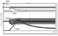
도 11a는 텅빈 충전 패드에 대해 송신기의 PA 입력 전류(1110, 1112) 및 AC 커플링된 PA 입력 전압(1120, 1122)의 예시적인 테스트 측정들을 도시한다. 트래이스들(1112, 1122)은 각각 트래이스들(1110 및 1120)의 확대된 뷰에 대응한다. 전류는 최종 값으로 상승한다는 것에 주의한다. 지연은 여기서 전류 감지 회로의 낮은 대역폭에 의해 유발된다. 도 11b는 무선 디바이스가 충전 패드 상에 배치될 때 송신기의 전류(1130, 1132) 및 전압(1140, 1142)의 예시적인 측정들을 도시한다. 트래이스들(1132, 1142)은 각각 트래이스들(1130 및 1140)의 확대된 뷰에 대응한다. 전류의 초기 스파이크는 충전 커패시터에 의해 유발되는 낮은 임피던스에 기인한다는 것에 주의한다. [0076]
11A illustrates exemplary test measurements of the
[0077]
도 12a-b에서, 송신기의 PA 입력 전류(1210, 1212) 및 AC 커플링된 PA 입력 전압(1220, 1222)이 재차 측정된다. 트래이스들(1212, 1222)은 각각 트래이스들(1210 및 1220)의 확대된 뷰에 대응한다. 도 12a의 예에서, (예를 들어, 적절한 수신 회로 없는 금속 객체 또는 일부 다른 디바이스일 수 있는) 로그(rogue) 디바이스는 그의 정류기 및 커패시터가 연결해제되어 있는 무선 전력 수신기를 이용함으로써 시뮬레이트된다. 따라서, 로그 디바이스는 개회로로서 "나타난다". 도 12a의 로그 디바이스 예는 도 11a의 텅빈 패드 경우와 매우 유사해 보인다는 것에 주의한다. 이러한 경우에, 유효한 디바이스는 검출되지 않을 것이다. 도 12b의 예에서, 정류기 및 커패시터가 재연결되고, 송신기의 전류(1230, 1232) 및 전압(1240, 1242)이 재차 측정된다. 트래이스들(1232, 1242)은 각각 트래이스들(1230 및 1240)의 확대된 뷰에 대응한다. 재차, 낮은 임피던스에 기인한 전류의 초기 스파이크가 충전 커패시터에 의해 유발된다는 것에 주의한다. 이러한 스파이크를 갖는 특징적인 파형은 유효한 디바이스의 검출을 허용하고 용이하게 한다. [0077]
12A-B, the
[0078]
도 13은 본 개시의 예시적인 실시예에 따라, 무선 전력 송신기의 충전 영역에의 무선 전력 수신기의 배치를 검출하기 위한 디바이스(1300)의 기능 블록도이다. 일 예에서, 디바이스(1300)는 송신 코일(1312)을 포함하고 수신기의 수신 코일에 전력을 무선으로 송신하도록 구성되는 송신 회로(1310)를 포함할 수 있다. 송신 회로(1310)는 도 4의 송신기(404) 및/또는 도 6의 송신 회로(600)의 하나 또는 그 초과의 컴포넌트들을 포함할 수 있으며, 이들의 세부사항들은 위에서 더 상세히 제공된다. [0078]
13 is a functional block diagram of a device 1300 for detecting the placement of a wireless power receiver in a charging area of a wireless power transmitter, in accordance with an exemplary embodiment of the present disclosure. In one example, the device 1300 may include a transmitting circuit 1310 that includes transmit
[0079]
또 다른 관련된 양상들에서, 송신 회로(1310)는 대기 전력을 감소시키면서, 송신 회로(1310)의 충전 영역에의 객체의 배치에 의해 유발되는 출력 임피던스의 변화들을 검출하기 위한 저전력 비콘 송신기(1314)를 포함할 수 있다. 비콘 송신기(1314)는 임피던스의 변화들을 검출하도록 송신 회로(1310)의 공진기에 쇼트(short) 비콘을 주기적으로 적용하도록 구성될 수 있다. 쇼트 비콘을 통해, 디바이스(1300)는 검출된 출력 임피던스의 리액턴스 및/또는 저항 변화를 감지 가능할 수 있다. 저전력 비콘 송신기(1314)는 쇼트 비콘으로 로드 변동을 검출 시에 더 높은 전력 상태를 개시하도록 추가로 구성될 수 있다. 예를 들어, 로드 변동의 검출에 대한 응답으로, 송신기(1314)는 쇼트 비콘보다 더 높거나 더 길 수 있는 "긴(long)" 비콘을 적용하도록 구성될 수 있다. "긴" 비콘은, 수신기가 송신기와의 통신을 설정하기에 충분한 전력을 갖도록 허용하기 위해 수신기에 충분한 전력을 제공하여 송신기(1314)가 더 높은 전력 상태들을 개시하게 허용할 수 있다. 관련된 양상들에서, 비콘 송신기(1314)는 송신 회로(1310)보단 오히려 검출 회로(1320)(아래에서 설명됨)의 부분일 수 있다. 또한, 비콘 송신기(1314)는 별개의 저전력 송신기일 수 있거나, 또는 대안적으로 더 낮은 전력에서 동작되는 주(primary) 전력 송신기일 수 있다. [0079]
In another related aspect, the transmit circuit 1310 includes a low
[0080]
디바이스(1300)는 송신기에 대해 제시되는 임피던스의 변화를 검출하도록 구성된 검출 회로(1320)를 또한 포함할 수 있으며, 이 변화는 수신기가 충전 영역에 배치되는 것에 대한 응답으로, 송신 및 수신 코일들 간에서 변경되거나 충전 영역에 적용되는 필드로부터 발생한다. 예를 들어, 검출 회로(1320)는 도 4의 송신기(404)의 로드 감지 회로(416) 등에 대응하거나 이를 포함할 수 있으며, 이들의 세부사항들은 위에서 더 상세히 제공된다. 관련된 양상들에서, 검출 회로(1320)는 필드의 초기 적용 동안 수신기의 커패시터(예를 들어, 필터 커패시터)의 충전과 연관되는 특징적 파형(예를 들어, 수신기에 대한 송신기 전류의 일시적 스파이크를 포함함)을 인지하기 위한 파형 검출기(1322)를 포함할 수 있다. 파형은 출력 임피던스, 송신기 전류 및/또는 송신기 전압에 기초하거나 관련될 수 있다. 보다 일반적으로, 검출 회로(1320)는 주어진 시간 인터벌 또는 기간 내에서 (예를 들어, 임피던스 또는 전류 응답 측정들 중 어느 하나를 통해) 임피던스 응답의 타입 또는 임피던스 변화 패턴을 검출하도록 구성될 수 있다. 특정 타입의 임피던스 변화/파형을 검출하기 위한 시간 인터벌/기간은 쇼트 비콘 동안 발생할 수 있다. [0080]
The device 1300 may also include a detection circuit 1320 configured to detect a change in the impedance presented to the transmitter, the change being determined in response to the receiver being placed in the charging area, Lt; RTI ID = 0.0 > and / or < / RTI > For example, the detection circuitry 1320 may correspond to or include the
[0081]
추가로 관련된 양상들에서, 검출 회로(1320)는 측정된 출력 임피던스의 슬로프(예를 들어, 도 9b의 트래이스) 등을 검출하기 위한 슬로프 검출 회로(1324)를 포함할 수 있다. 또 다른 관련된 양상들에서, 검출 회로(1320)는 파형(들)을 샘플링하고 샘플링된 파형(들)의 신호 파라미터들을 결정하기 위해 임의의 프로세싱/필터링을 수행하도록 자신 내에 프로그래밍되는 디지털 신호 프로세싱(1328)을 선택적으로 가질 수 있는 전용 프로세서(1326)를 포함할 수 있다. 또 다른 관련된 양상들에서, 위의 프로세싱 작업들은 기존의 프로세서의 자원들을 공유할 수 있다. 추가로 관련된 양상들에서, 비콘 송신기(1314)는 송신 회로(1310)보단 오히려 검출 회로(1320)의 부분일 수 있다. [0081]
In further related aspects, the detection circuit 1320 may include a
[0082]
도 14는 본 개시의 하나 또는 그 초과의 양상들에 따라, 무선 전력 송신기의 충전 영역에서 무선 전력 수신기를 무선 충전하고, 특히 그의 배치를 검출하기 위한 예시적인 방법(1400)의 흐름도를 제공한다. 방법(1400)이 특정 순서를 참조하여 본원에서 설명되지만, 다양한 구현들에서, 본원에서의 단계(들) 또는 특징(들)은 상이한 순서로 수행될 수 있거나, 또는 생략될 수 있거나, 또는 부가적인 단계(들)/특징(들)을 포함할 수 있다. 예를 들어, 방법(1400)은 무선 전력 송신기(예를 들어, 도 13의 디바이스(1300)) 또는 그의 컴포넌트(들)에 의해 동작 가능할 수 있다. [0082]
14 provides a flow diagram of an
[0083]
방법(1400)은, 1410에서, 송신 회로의 송신 코일을 통해 수신기의 수신 코일로 충전 영역에 적용되는 무선 필드를 통하여 전력을 송신하는 것을 포함할 수 있다. 일 구현에서, 블록(1410)은 도 13의 송신 회로(1310) 또는 그의 컴포넌트(들)에 의해 수행될 수 있다. 방법(1400)은, 1420에서, 수신기가 충전 영역에 배치되는 것에 대한 응답으로, 송신 및 수신 코일들 간에 변하거나 충전 영역에 적용되는 필드로부터 발생하는 특징적 파형을 검출하는 것을 포함할 수 있다. 일 구현에서, 블록(1420)은 도 13의 검출 회로(1320) 또는 그의 컴포넌트(들)에 의해 수행될 수 있다. 특징적 파형은 필드의 초기 적용 동안 수신기의 커패시터의 충전과 연관될 수 있고, 수신기가 충전 영역에 배치되는 것에 대한 응답으로 송신기의 송신 회로에 제시되는 임피던스의 변화에 적어도 부분적으로 기초할 수 있다. [0083]
The
[0084]
도 15를 참조하면, 방법(1400)을 수행하기 위해 요구되진 않는 선택적인 방법(1400)의 추가의 동작들 또는 양상들이 도시된다. 방법(1400)이 도 15의 적어도 하나의 블록을 포함하는 경우, 방법(1400)은, 예시될 수 있는 임의의 후속 다운스트림 블록(들)을 반드시 포함해야 할 필요 없이, 적어도 하나의 블록 이후에 종결될 수 있다. 관련된 양상들에서, 블록(1420)은, 1430에서, 필드의 초기 적용 동안 수신기의 커패시터의 충전과 연관되는 임피던스 패턴 변화를 인지하는 것을 포함할 수 있다. [0084]
Referring to FIG. 15, additional operations or aspects of an
[0085] 추가로 관련된 양상들에서, 특징적인 파형은 송신기 전압 및 송신기 전류에 기초하여 계산되는 바와 같은 저항의 일시적 스파이크를 포함할 수 있고, 송신기 전압은 AC 전압을 포함할 수 있고 송신기 전류는 AC 전류를 포함한다. 예를 들어, 블록(1420)은, 1440에서, AC 경로의 실질적으로 동일 지점에서 AC 전압 및 AC 전류를 측정하는 것을 포함할 수 있다. 다른 예에서, 블록(1420)은, 1450에서, AC 경로의 제 1 지점에서 AC 전류를 측정하는 것을 포함할 수 있으며, AC 전류는 위상 및 진폭 중 적어도 하나 면에서, AC 전압이 측정되는 AC 경로의 제 2 지점에서 측정되는 대응하는 AC 전류에 관하여 알려진 관계를 갖는다. [0085] In further related aspects, the characteristic waveform may comprise a transient spike of the resistance as computed based on the transmitter voltage and the transmitter current, the transmitter voltage may comprise an AC voltage, and the transmitter current may comprise an AC current do. For example, block 1420 may include, at 1440, measuring the AC voltage and AC current at substantially the same point in the AC path. In another example, block 1420 may include measuring an AC current at a first point of the AC path at 1450, wherein the AC current is measured in at least one of the phase and amplitude, Lt; RTI ID = 0.0 > AC < / RTI >
[0086] 또 다른 관련된 양상들에서, 특징적인 파형은 송신기 전압 및 송신기 전류에 기초하여 계산되는 바와 같은 저항의 일시적 스파이크를 포함할 수 있고, 송신기 전압은 DC 전압을 포함할 수 있고 송신기 전류는 DC 전류를 포함한다. 예를 들어, 블록(1420)은, 1460에서, DC 경로의 제 1 지점에서 DC 전류를 측정하는 것을 포함할 수 있으며, DC 전류는 DC 전압이 측정되는 제 2 지점에서 측정된 대응하는 DC 전류에 관하여 값 면에서 알려진 관계를 갖는다. [0086] In other related aspects, the characteristic waveform may include a transient spike of the resistance as calculated based on the transmitter voltage and the transmitter current, the transmitter voltage may include a DC voltage, and the transmitter current may include a DC current do. For example, block 1420 may comprise measuring a DC current at a first point of the DC path at 1460, wherein the DC current is measured at a first point of the DC path, Have a known relationship in terms of value.
[0087]
또 다른 관련된 양상들에서, 방법(1400)은 추가로, 1470에서, 수신기가 충전 영역에 있게 되는 것에 대한 응답으로 전력-절감 모드로부터 더 높은 전력 모드로 송신기를 스위칭하는 것을 포함할 수 있다. [0087]
In another related aspect, the
[0088] 위에서 설명된 방법들의 다양한 동작들은 다양한 하드웨어 및/또는 소프트웨어 컴포넌트(들), 회로들, 및/또는 모듈(들)과 같이 동작들을 수행 가능한 임의의 적합한 수단에 의해 수행될 수 있다. 일반적으로, 도면들에서 예시되는 임의의 동작들은, 그 동작들을 수행할 수 있는 대응하는 기능 수단에 의해 수행될 수 있다. 일 양상에서, 충전 영역에 적용된 무선 필드를 통해 전력을 수신기의 수신 코일에 송신하기 위한 수단은, 예를 들어, 송신 코일, 비콘 송신기, 전력 증폭기 및/또는 송신 회로의 다른 컴포넌트(들)를 포함할 수 있다. [0088] The various operations of the methods described above may be performed by any suitable means capable of performing operations such as various hardware and / or software component (s), circuits, and / or module (s). In general, any of the operations illustrated in the Figures may be performed by corresponding functional means capable of performing the operations. In an aspect, the means for transmitting power to a receiver coil of a receiver via a radio field applied to a charging region includes, for example, a transmission coil, a beacon transmitter, a power amplifier and / or other component (s) of a transmission circuit can do.
[0089] 다른 양상에서, 수신기가 충전 영역에 배치되는 것에 대한 응답으로, 특징적 파형을 검출하기 위한 수단은, 예를 들어, 로드 감지 회로; 필드의 초기 적용 동안 수신기의 커패시터의 충전과 연관되는 특징적인 파형을 인지하기 위한 파형 검출기; 측정된 출력 임피던스의 슬로프를 검출하기 위한 슬로프 검출기; 전용 프로세서/제어기; 및/또는 검출 회로의 다른 컴포넌트(들)를 포함할 수 있다. [0089] In another aspect, in response to the receiver being located in the charging region, the means for detecting the characteristic waveform may include, for example, a load sensing circuit; A waveform detector for sensing a characteristic waveform associated with charging of a capacitor of the receiver during an initial application of the field; A slope detector for detecting a slope of the measured output impedance; Dedicated processor / controller; And / or other component (s) of the detection circuitry.
[0090] 또 다른 양상에서, 특징적 파형을 검출하거나 또는 필드의 초기 적용 동안 수신기의 커패시터의 충전과 연관되는 임피던스 변화 패턴을 인지하기 위한 수단은 예를 들어, 필드의 초기 적용 동안 수신기의 커패시터의 충전과 연관되는 특징적 파형 또는 패턴(예를 들어, 수신기로의 송신기 전류의 일시적 스파이크를 포함함)을 인기하기 위한 파형 검출기를 포함할 수 있다. [0090] In yet another aspect, a means for detecting a characteristic waveform or for recognizing an impedance variation pattern associated with the charging of a capacitor of a receiver during initial application of a field may include, for example, And may include a waveform detector to popularize a characteristic waveform or pattern (e.g., including a transient spike of transmitter current to the receiver).
[0091] 또 다른 양상에서, AC 경로의 실질적으로 동일한 지점에서 AC 전압 및 AC 전류를 측정하기 위한 수단은 예를 들어, 로드 감지 회로, 파형 검출기, 슬로프 검출기, 프로세서/제어기 및/또는 검출 회로의 다른 컴포넌트(들)를 포함할 수 있다. [0091] In yet another aspect, the means for measuring the AC voltage and the AC current at substantially the same point in the AC path may include, for example, a load sensing circuit, a waveform detector, a slope detector, a processor / controller and / Lt; / RTI >
[0092] 다른 양상에서, AC 경로의 제 1 지점에서 AC 전류를 측정하기 위한 수단은 예를 들어, 로드 감지 회로, 파형 검출기, 슬로프 검출기, 프로세서/제어기 및/또는 검출 회로의 다른 컴포넌트(들)를 포함할 수 있다. [0092] In another aspect, the means for measuring AC current at a first point of the AC path includes, for example, a load sensing circuit, a waveform detector, a slope detector, a processor / controller and / or other component (s) .
[0093] 정보 및 신호들이 다양한 다른 기술들 및 기법들 중 임의의 것을 이용하여 표현될 수 있다. 예를 들어, 위의 설명 전반에 걸쳐 참조될 수 있는 데이터, 명령들, 커맨드들, 정보, 신호들, 비트들, 심볼들 및 칩들은 전압들, 전류들, 전자기파들, 자기 필드들 또는 자기 입자들, 광 필드들 또는 광 입자들, 또는 이들의 임의의 결합으로 표현될 수 있다. [0093] Information and signals may be represented using any of a variety of different technologies and techniques. For example, data, instructions, commands, information, signals, bits, symbols, and chips that may be referenced throughout the above description may refer to voltages, currents, electromagnetic waves, magnetic fields, , Light fields or light particles, or any combination thereof.
[0094] 본원에서 개시된 실시예들과 관련하여 설명된 다양한 예시적인 로직 블록들, 모듈들, 회로들, 및 알고리즘 단계들은, 전자 하드웨어, 컴퓨터 소프트웨어, 또는 이 둘의 결합으로 구현될 수 있다. 하드웨어와 소프트웨어의 상호 교환 가능성을 명확하게 설명하기 위해, 다양한 예시적인 컴포넌트들, 블록들, 모듈들, 회로들, 및 단계들이 이들의 기능성의 견지에서 일반적으로 상술되었다. 이러한 기능이 하드웨어 또는 소프트웨어로 구현되는지 여부는 전체 시스템에 부과되는 설계 제약들 및 특정 애플리케이션에 의존한다. 설명된 기능성이 각각의 특정 애플리케이션 마다 다양한 방식들로 구현할 수 있지만, 이러한 구현 판단들은 본 발명의 실시예들의 범위를 벗어나게 하는 것으로 해석되어서는 안 된다. [0094] The various illustrative logical blocks, modules, circuits, and algorithm steps described in connection with the embodiments disclosed herein may be implemented as electronic hardware, computer software, or combinations of both. In order to clearly illustrate the interchangeability of hardware and software, various illustrative components, blocks, modules, circuits, and steps have been described above generally in terms of their functionality. Whether such functionality is implemented as hardware or software depends upon the particular application and design constraints imposed on the overall system. While the described functionality may be implemented in various ways for each particular application, such implementation decisions should not be interpreted as causing a departure from the scope of embodiments of the present invention.
[0095] 본 명세서에 개시된 실시예와 관련하여 설명된 다양한 예시적인 블록, 모듈, 및 회로들은, 범용 프로세서, 디지털 신호 프로세서(DSP), 주문형 집적 회로(ASIC), 필드 프로그래밍 가능 게이트 어레이(FPGA), 또는 기타 프로그래밍 가능 로직 디바이스, 이산 게이트 또는 트랜지스터 로직, 이산 하드웨어 컴포넌트, 또는 본원에 설명된 기능을 수행하도록 설계된 이들의 임의의 결합으로 구현 또는 수행될 수 있다 범용 프로세서는 마이크로프로세서일 수 있지만, 대안적으로, 프로세서는 임의의 종래 프로세서, 제어기, 마이크로 제어기, 또는 상태 머신일 수 있다. 프로세서는 또한 컴퓨팅 디바이스들의 결합, 예를 들어, DSP와 마이크로프로세서의 결합, 복수의 마이크로프로세서들, DSP 코어와 연결된 하나 또는 그 초과의 마이크로프로세서들 또는 임의의 다른 이러한 구성으로서 구현될 수 있다. [0095] The various illustrative blocks, modules, and circuits described in connection with the embodiments disclosed herein may be implemented or performed with a general purpose processor, a digital signal processor (DSP), an application specific integrated circuit (ASIC), a field programmable gate array (FPGA) Programmable logic device, discrete gate or transistor logic, discrete hardware components, or any combination thereof designed to perform the functions described herein. A general purpose processor may be a microprocessor, but, alternatively, The processor may be any conventional processor, controller, microcontroller, or state machine. The processor may also be implemented as a combination of computing devices, e.g., a combination of a DSP and a microprocessor, a plurality of microprocessors, one or more microprocessors in conjunction with a DSP core, or any other such configuration.
[0096] 본원에 개시된 실시예들과 관련하여 설명된 알고리즘 또는 방법의 단계들 및 기능들은 직접 하드웨어, 프로세서에 의해 실행되는 소프트웨어 모듈, 또는 이 둘의 결합으로 구현될 수 있다. 소프트웨어로 구현되는 경우, 기능들은 하나 이상의 명령들 또는 코드로서 유형(tangible)의 비-일시적인 컴퓨터 판독 가능 매체 상에 저장되거나 이로써 전송될 수 있다. 소프트웨어 모듈은 RAM(Random Access Memory), 플래시 메모리, ROM(Read Only Memory), EPROM(Electrically Programmable ROM), EEPROM(Electrically Erasable Programmable ROM), 레지스터들, 하드 디스크, 제거 가능 디스크, CD-ROM, 또는 당 분야에 알려진 임의의 다른 형태의 저장 매체에 상주할 수 있다 저장 매체는 프로세서에 커플링되어, 프로세서는 저장 매체로부터 정보를 판독하고, 저장 매체에 정보를 기록할 수 있다. 대안적으로, 저장 매체는 프로세서에 통합될 수 있다. 본원에서 이용된 바와 같은 디스크(disk) 및 디스크(disc)는 컴팩트 디스크(disc)(CD), 레이저 디스크(disc), 광 디스크(disc), 디지털 다용도 디스크(disc)(DVD), 플로피 디스크(disk), 및 블루-레이 디스크(disc)를 포함하며, 여기서 디스크(disk)는 보통 데이터를 자기적으로 재생하지만, 디스크(disc)는 레이저를 통해 광학적으로 데이터를 재생한다. 이들의 결합은 또한 컴퓨터 판독 가능 매체들의 범위 내에 포함되어야 한다. 프로세서 및 저장 매체는 ASIC에 상주할 수 있다 ASIC는 사용자 단말에 상주할 수 있다. 대안적으로, 프로세서 및 저장 매체는 사용자 단말에서 개별 컴포넌트들로서 상주할 수 있다. [0096] The steps and functions of the algorithm or method described in connection with the embodiments disclosed herein may be embodied directly in hardware, in a software module executed by a processor, or in a combination of the two. When implemented in software, the functions may be stored on or transmitted over a tangible non-transitory computer readable medium as one or more instructions or code. The software modules may be stored in a computer-readable recording medium, such as a RAM (Random Access Memory), a flash memory, a ROM (Read Only Memory), an EPROM (Electrically Programmable ROM), an Electrically Erasable Programmable ROM (EEPROM) And may reside in any other form of storage medium known in the art. A storage medium is coupled to the processor such that the processor can read information from, and write information to, the storage medium. Alternatively, the storage medium may be integrated into the processor. Disks and discs as used herein are intended to include any type of disc such as a compact disc (CD), a laser disc, an optical disc, a digital versatile disc (DVD), a floppy disc disk, and a Blu-ray disc, wherein the disc usually reproduces the data magnetically, while the disc reproduces the data optically through the laser. Combinations of these should also be included within the scope of computer readable media. The processor and the storage medium may reside in an ASIC. The ASIC may reside in a user terminal. In the alternative, the processor and the storage medium may reside as discrete components in a user terminal.
[0097] 본 개시를 요약할 목적으로, 본 발명들의 특정 양상들, 이점들 및 신규한 특징들이 본원에서 설명되었다. 이러한 모든 이점들이 본 발명의 임의의 특정 실시예들에 따라 반드시 달성될 필요는 없다는 것이 이해될 것이다. 따라서, 본 발명은 본원에서 교시되거나 제안될 수 있는 바와 같은 다른 이점들을 반드시 달성할 필요 없이, 본원에서 교시된 바와 같은 하나의 이점 또는 이점들의 그룹을 달성하거나 최적화하는 방식으로 실현되거나 수행될 수 있다. [0097] For the purpose of summarizing the present disclosure, certain aspects, advantages and novel features of the invention have been described herein. It will be appreciated that all of these advantages need not necessarily be achieved in accordance with any particular embodiment of the present invention. Thus, the present invention may be realized or carried out in a manner that accomplishes or optimizes one advantage or group of advantages as taught herein, without necessarily requiring other advantages, such as may be taught or suggested herein .
[0098] 위에서 설명된 실시예들의 다양한 변형들은 쉽게 자명하게 될 것이며, 본원에서 정의된 일반적인 원리들은 본 발명의 사상 또는 범위를 벗어나지 않고 다른 실시예들에 적용될 수도 있다. 따라서 본 발명은 본원에서 도시된 실시예들로 제한되도록 의도되는 것이 아니라, 본원에서 개시된 신규한 특징들 및 원리들에 부합하는 최광의의 범위로 허여되어야 한다. [0098] Various modifications of the embodiments described above will be readily apparent, and the generic principles defined herein may be applied to other embodiments without departing from the spirit or scope of the invention. Accordingly, the present invention is not intended to be limited to the embodiments shown herein but is to be accorded the widest scope consistent with the novel features and principles disclosed herein.
Claims (30)
송신 코일을 포함하고 충전 영역에 적용되는 무선 필드(wireless field)를 통해 전력을 수신기의 수신 코일에 무선으로 송신하도록 구성된 송신 회로; 및
상기 수신기가 상기 충전 영역에 배치되는 것에 대한 응답으로, 상기 송신 및 수신 코일들 간에 변하거나 또는 적용되는 필드로부터 발생하는 파형의 특성을 검출하도록 구성되는 검출 회로
를 포함하는,
무선 전력 송신기의 충전 영역에의 무선 전력 수신기의 배치를 검출하기 위한 디바이스.
A device for detecting the placement of a wireless power receiver in a charging area of a wireless power transmitter,
A transmitting circuit configured to wirelessly transmit power to a receive coil of a receiver via a wireless field including a transmit coil and applied to a fill region; And
A detection circuit configured to detect a characteristic of a waveform occurring in a field that varies or is applied between the transmit and receive coils in response to the receiver being located in the fill region;
/ RTI >
A device for detecting the placement of a wireless power receiver in a charging area of a wireless power transmitter.
상기 파형의 특성은 상기 필드의 초기 적용 동안 상기 수신기의 커패시터의 충전과 연관되고, 상기 수신기가 상기 충전 영역에 배치되는 것에 대한 응답으로 상기 송신기의 송신 회로에 제시되는 임피던스의 변화에 적어도 부분적으로 기초하는,
무선 전력 송신기의 충전 영역에의 무선 전력 수신기의 배치를 검출하기 위한 디바이스.
The method according to claim 1,
The characteristics of the waveform being associated with the charging of the capacitor of the receiver during the initial application of the field and being based at least in part on a change in the impedance presented to the transmitter circuit of the transmitter in response to the receiver being placed in the charging area doing,
A device for detecting the placement of a wireless power receiver in a charging area of a wireless power transmitter.
상기 파형의 특성은 상기 필드의 초기 적용 동안 상기 수신기의 커패시터의 충전과 연관되는 임피던스 변화 패턴을 나타내는,
무선 전력 송신기의 충전 영역에의 무선 전력 수신기의 배치를 검출하기 위한 디바이스.
The method according to claim 1,
Wherein the characteristic of the waveform is indicative of an impedance variation pattern associated with the charging of the capacitor of the receiver during an initial application of the field,
A device for detecting the placement of a wireless power receiver in a charging area of a wireless power transmitter.
상기 파형의 특성은 송신기 전류의 일시적 스파이크(transient spike)를 포함하는,
무선 전력 송신기의 충전 영역에의 무선 전력 수신기의 배치를 검출하기 위한 디바이스.
The method according to claim 1,
The characteristics of the waveform include a transient spike of the transmitter current.
A device for detecting the placement of a wireless power receiver in a charging area of a wireless power transmitter.
상기 송신기 전류는 상기 송신기의 전력 증폭기(PA)로의 DC 전류를 포함하는,
무선 전력 송신기의 충전 영역에의 무선 전력 수신기의 배치를 검출하기 위한 디바이스.
5. The method of claim 4,
Wherein the transmitter current comprises a DC current to a power amplifier (PA) of the transmitter,
A device for detecting the placement of a wireless power receiver in a charging area of a wireless power transmitter.
상기 파형의 특성은 송신기 전압의 일시적 스파이크 또는 오실레이션(oscillation)을 포함하는,
무선 전력 송신기의 충전 영역에의 무선 전력 수신기의 배치를 검출하기 위한 디바이스.
The method according to claim 1,
The characteristics of the waveform include transient spikes or oscillations of the transmitter voltage.
A device for detecting the placement of a wireless power receiver in a charging area of a wireless power transmitter.
상기 송신기 전압은 상기 송신기의 전력 증폭기(PA)에 공급되는 DC 전압을 포함하는,
무선 전력 송신기의 충전 영역에의 무선 전력 수신기의 배치를 검출하기 위한 디바이스.
The method according to claim 6,
Wherein the transmitter voltage comprises a DC voltage supplied to a power amplifier (PA) of the transmitter.
A device for detecting the placement of a wireless power receiver in a charging area of a wireless power transmitter.
상기 파형의 특성은 송신기 전압 및 송신기 전류에 기초하여 계산된 바와 같은 저항의 일시적 스파이크를 포함하는,
무선 전력 송신기의 충전 영역에의 무선 전력 수신기의 배치를 검출하기 위한 디바이스.
The method according to claim 1,
The characteristics of the waveform include transient spikes of the resistance as calculated based on the transmitter voltage and the transmitter current.
A device for detecting the placement of a wireless power receiver in a charging area of a wireless power transmitter.
상기 송신기 전압은 AC 전압을 포함하고, 상기 송신기 전류는 AC 전류를 포함하는,
무선 전력 송신기의 충전 영역에의 무선 전력 수신기의 배치를 검출하기 위한 디바이스.
9. The method of claim 8,
Wherein the transmitter voltage comprises an AC voltage and the transmitter current comprises an AC current.
A device for detecting the placement of a wireless power receiver in a charging area of a wireless power transmitter.
상기 AC 전압 및 상기 AC 전류는 AC 경로의 실질적으로 동일 지점에서 측정되는,
무선 전력 송신기의 충전 영역에의 무선 전력 수신기의 배치를 검출하기 위한 디바이스.
10. The method of claim 9,
Wherein the AC voltage and the AC current are measured at substantially the same point in the AC path,
A device for detecting the placement of a wireless power receiver in a charging area of a wireless power transmitter.
상기 AC 전류는 AC 경로의 제 1 지점에서 측정되고, 상기 AC 전압이 측정되는 AC 경로의 제 2 지점에서 측정되는 대응하는 AC 전류에 관하여 상기 AC 전류는 위상 및 진폭 중 적어도 하나 면에서 알려진 관계를 갖는,
무선 전력 송신기의 충전 영역에의 무선 전력 수신기의 배치를 검출하기 위한 디바이스.
10. The method of claim 9,
The AC current is measured at a first point of the AC path and the AC current with respect to a corresponding AC current measured at a second point of the AC path at which the AC voltage is measured has a known relationship in at least one of phase and amplitude Having,
A device for detecting the placement of a wireless power receiver in a charging area of a wireless power transmitter.
상기 송신기 전압은 DC 전압을 포함하고, 상기 송신기 전류는 DC 전류를 포함하는,
무선 전력 송신기의 충전 영역에의 무선 전력 수신기의 배치를 검출하기 위한 디바이스.
9. The method of claim 8,
Wherein the transmitter voltage comprises a DC voltage and the transmitter current comprises a DC current.
A device for detecting the placement of a wireless power receiver in a charging area of a wireless power transmitter.
상기 DC 전압 및 상기 DC 전류는 DC 경로의 실질적으로 동일 지점에서 측정되는,
무선 전력 송신기의 충전 영역에의 무선 전력 수신기의 배치를 검출하기 위한 디바이스.
13. The method of claim 12,
Wherein the DC voltage and the DC current are measured at substantially the same point in the DC path,
A device for detecting the placement of a wireless power receiver in a charging area of a wireless power transmitter.
상기 DC 전류는 DC 경로의 제 1 지점에서 측정되고, 상기 DC 전류는 상기 DC 전압이 측정되는 제 2 지점에서 측정되는 대응하는 DC 전류에 관하여 값 면에서 알려진 관계를 갖는,
무선 전력 송신기의 충전 영역에의 무선 전력 수신기의 배치를 검출하기 위한 디바이스.
13. The method of claim 12,
Wherein the DC current is measured at a first point of the DC path and the DC current has a known value relationship with respect to a corresponding DC current measured at a second point at which the DC voltage is measured,
A device for detecting the placement of a wireless power receiver in a charging area of a wireless power transmitter.
상기 검출 회로는 추가로, 상기 수신기가 상기 충전 영역에 있게 되는 것에 대한 응답으로, 전력-절감 모드로부터 더 높은 전력 모드로 상기 송신기를 스위칭하도록 구성되는,
무선 전력 송신기의 충전 영역에의 무선 전력 수신기의 배치를 검출하기 위한 디바이스.
The method according to claim 1,
Wherein the detection circuit is further configured to switch the transmitter from a power-saving mode to a higher power mode in response to the receiver being in the charging area,
A device for detecting the placement of a wireless power receiver in a charging area of a wireless power transmitter.
상기 검출 회로는 추가로, 유효 수신기가 상기 충전 영역에 배치되는 것에 대한 응답으로, 상기 송신기에 제시되는 임피던스의 변화를 검출하도록 구성되고, 상기 유효 수신기는 연결된 상태들의 정류기 및 커패시터를 갖는 수신기 회로를 포함하고, 상기 커패시터는 상기 필드의 초기 적용 동안 충전하도록 구성되는,
무선 전력 송신기의 충전 영역에의 무선 전력 수신기의 배치를 검출하기 위한 디바이스.
The method according to claim 1,
Wherein the detection circuit is further configured to detect a change in the impedance presented to the transmitter in response to the effective receiver being disposed in the charging region, the effective receiver comprising a receiver circuit having a rectifier and a capacitor in connected states Wherein the capacitor is configured to charge during an initial application of the field,
A device for detecting the placement of a wireless power receiver in a charging area of a wireless power transmitter.
송신 회로의 송신 코일을 통해 수신기의 수신 코일로 상기 충전 영역에 적용되는 무선 필드를 통하여 전력을 송신하는 단계; 및
상기 수신기가 상기 충전 영역에 배치되는 것에 대한 응답으로, 상기 송신 및 수신 코일들 간에 변하거나 또는 적용되는 필드로부터 발생하는 파형의 특성을 검출하는 단계
를 포함하는,
무선 전력 송신기의 충전 영역에의 무선 전력 수신기의 배치를 검출하기 위한 방법.
CLAIMS 1. A method for detecting placement of a wireless power receiver in a charging area of a wireless power transmitter,
Transmitting power through a radio field applied to the charging region to a receiver coil of the receiver through a transmission coil of the transmission circuit; And
Detecting, in response to the receiver being placed in the charging area, a characteristic of a waveform occurring between the transmitting and receiving coils,
/ RTI >
A method for detecting the placement of a wireless power receiver in a charging area of a wireless power transmitter.
상기 파형의 특성을 검출하는 단계는, 상기 필드의 초기 적용 동안 상기 수신기의 커패시터의 충전과 연관되는 임피던스 변화 패턴을 인지하는 단계를 포함하는,
무선 전력 송신기의 충전 영역에의 무선 전력 수신기의 배치를 검출하기 위한 방법.
18. The method of claim 17,
Wherein detecting the characteristic of the waveform comprises recognizing an impedance variation pattern associated with the charging of the capacitor of the receiver during an initial application of the field.
A method for detecting the placement of a wireless power receiver in a charging area of a wireless power transmitter.
상기 파형의 특성은 송신기 전압 및 송신기 전류에 기초하여 계산된 바와 같은 저항의 일시적 스파이크를 포함하는,
무선 전력 송신기의 충전 영역에의 무선 전력 수신기의 배치를 검출하기 위한 방법.
18. The method of claim 17,
The characteristics of the waveform include transient spikes of the resistance as calculated based on the transmitter voltage and the transmitter current.
A method for detecting the placement of a wireless power receiver in a charging area of a wireless power transmitter.
상기 송신기 전압은 AC 전압을 포함하고, 상기 송신기 전류는 AC 전류를 포함하고,
상기 파형의 특성을 검출하는 단계는 AC 경로의 실질적으로 동일 지점에서 상기 AC 전압 및 상기 AC 전류를 측정하는 단계를 포함하는,
무선 전력 송신기의 충전 영역에의 무선 전력 수신기의 배치를 검출하기 위한 방법.
20. The method of claim 19,
Wherein the transmitter voltage comprises an AC voltage, the transmitter current comprises an AC current,
Wherein detecting the characteristic of the waveform comprises measuring the AC voltage and the AC current at substantially the same point in the AC path.
A method for detecting the placement of a wireless power receiver in a charging area of a wireless power transmitter.
상기 파형의 특성을 검출하는 단계는, AC 경로의 제 1 지점에서 상기 AC 전류 측정하는 단계를 포함하며, 상기 AC 전류는 상기 AC 전압이 측정되는 AC 경로의 제 2 지점에서 측정되는 대응하는 AC 전류에 관하여 위상 및 진폭 중 적어도 하나 면에서 알려진 관계를 갖는,
무선 전력 송신기의 충전 영역에의 무선 전력 수신기의 배치를 검출하기 위한 방법.
20. The method of claim 19,
Wherein detecting the characteristic of the waveform comprises measuring the AC current at a first point of the AC path, the AC current having a corresponding AC current measured at a second point of the AC path at which the AC voltage is measured Having a known relationship in at least one of phase and amplitude,
A method for detecting the placement of a wireless power receiver in a charging area of a wireless power transmitter.
상기 파형의 특성은 송신기 전압 및 송신기 전류에 기초하여 계산된 바와 같은 저항의 일시적 스파이크를 포함하는,
무선 전력 송신기의 충전 영역에의 무선 전력 수신기의 배치를 검출하기 위한 방법.
18. The method of claim 17,
The characteristics of the waveform include transient spikes of the resistance as calculated based on the transmitter voltage and the transmitter current.
A method for detecting the placement of a wireless power receiver in a charging area of a wireless power transmitter.
상기 송신기 전압은 DC 전압을 포함하고, 상기 송신기 전류는 DC 전류를 포함하고,
상기 파형의 특성을 검출하는 단계는 DC 경로의 제 1 지점에서 상기 DC 전류를 측정하는 단계를 포함하며, 상기 DC 전류는 상기 DC 전압이 측정되는 제 2 지점에서 측정되는 대응하는 DC 전류에 관하여 값 면에서 알려진 관계를 갖는,
무선 전력 송신기의 충전 영역에의 무선 전력 수신기의 배치를 검출하기 위한 방법.
23. The method of claim 22,
Wherein the transmitter voltage comprises a DC voltage, the transmitter current comprises a DC current,
Wherein detecting the characteristic of the waveform comprises measuring the DC current at a first point of the DC path, the DC current having a value with respect to a corresponding DC current measured at a second point at which the DC voltage is measured In this way,
A method for detecting the placement of a wireless power receiver in a charging area of a wireless power transmitter.
상기 수신기가 상기 충전 영역에 있게 되는 것에 대한 응답으로, 전력-절감 모드로부터 더 높은 전력 모드로 상기 송신기를 스위칭하는 단계
를 더 포함하는,
무선 전력 송신기의 충전 영역에의 무선 전력 수신기의 배치를 검출하기 위한 방법.18. The method of claim 17,
Switching the transmitter from a power-saving mode to a higher power mode in response to the receiver being in the charging zone
≪ / RTI >
A method for detecting the placement of a wireless power receiver in a charging area of a wireless power transmitter.
수신기의 수신 코일로 상기 충전 영역에 적용되는 무선 필드를 통하여 전력을 송신하기 위한 수단; 및
상기 수신기가 상기 충전 영역에 배치되는 것에 대한 응답으로, 상기 송신하기 위한 수단과 상기 수신 코일 간에 변하거나 또는 적용되는 필드로부터 발생하는 파형의 특성을 검출하기 위한 수단
을 포함하는,
충전 영역에의 무선 전력 수신기의 배치를 검출하기 위한 장치.
An apparatus for detecting the placement of a wireless power receiver in a charging area,
Means for transmitting power through a radio field applied to the charging region of the receiver coil; And
Means for detecting a characteristic of a waveform originating from a field that changes or is applied between the means for transmitting and the receiving coil in response to the receiver being located in the charging region;
/ RTI >
An apparatus for detecting the placement of a wireless power receiver in a charging area.
상기 파형의 특성을 검출하기 위한 수단은, 상기 필드의 초기 적용 동안 상기 수신기의 커패시터의 충전과 연관되는 임피던스 변화 패턴을 인지하기 위한 수단을 포함하는,
충전 영역에의 무선 전력 수신기의 배치를 검출하기 위한 장치.
26. The method of claim 25,
Wherein the means for detecting a characteristic of the waveform comprises means for recognizing an impedance change pattern associated with the charging of a capacitor of the receiver during an initial application of the field,
An apparatus for detecting the placement of a wireless power receiver in a charging area.
상기 파형의 특성은 송신기 전압 및 송신기 전류에 기초하여 계산된 바와 같은 저항의 일시적 스파이크를 포함하고,
상기 송신기 전압은 AC 전압을 포함하고, 상기 송신기 전류는 AC 전류를 포함하는,
충전 영역에의 무선 전력 수신기의 배치를 검출하기 위한 장치.
26. The method of claim 25,
The characteristics of the waveform include transient spikes of the resistance as calculated based on the transmitter voltage and the transmitter current,
Wherein the transmitter voltage comprises an AC voltage and the transmitter current comprises an AC current.
An apparatus for detecting the placement of a wireless power receiver in a charging area.
상기 파형의 특성을 검출하기 위한 수단은 AC 경로의 실질적으로 동일 지점에서 상기 AC 전압 및 상기 AC 전류를 측정하기 위한 수단을 포함하는,
충전 영역에의 무선 전력 수신기의 배치를 검출하기 위한 장치.
28. The method of claim 27,
Wherein the means for detecting the characteristics of the waveform comprises means for measuring the AC voltage and the AC current at substantially the same point in the AC path.
An apparatus for detecting the placement of a wireless power receiver in a charging area.
상기 파형의 특성을 검출하기 위한 수단은, AC 경로의 제 1 지점에서 상기 AC 전류 측정하기 위한 수단을 포함할 수 있으며, 상기 AC 전류는 상기 AC 전압이 측정되는 AC 경로의 제 2 지점에서 측정되는 대응하는 AC 전류에 관하여 위상 및 진폭 중 적어도 하나 면에서 알려진 관계를 갖는,
충전 영역에의 무선 전력 수신기의 배치를 검출하기 위한 장치.
28. The method of claim 27,
The means for detecting the characteristics of the waveform may comprise means for measuring the AC current at a first point of the AC path and the AC current is measured at a second point of the AC path at which the AC voltage is measured Having a known relationship in at least one of a phase and an amplitude with respect to a corresponding AC current,
An apparatus for detecting the placement of a wireless power receiver in a charging area.
송신 회로의 송신 코일을 통해 수신기의 수신 코일로 충전 영역에 적용되는 무선 필드를 통하여 전력을 송신하게 하고, 그리고
상기 수신기가 상기 충전 영역에 배치되는 것에 대한 응답으로, 상기 송신 및 수신 코일들 간에 변하거나 또는 적용되는 필드로부터 발생하는 파형의 특성을 검출하게 하는,
비-일시적인 컴퓨터 판독 가능 매체.21. A non-transitory computer readable medium comprising code, wherein the code, when executed,
To transmit power through the radio field applied to the charging region to the receiver coil of the receiver via the transmission coil of the transmission circuit, and
In response to the receiver being placed in the charging region, detecting a characteristic of a waveform that originates from a field that varies or is applied between the transmitting and receiving coils,
Non-transient computer readable medium.
Applications Claiming Priority (5)
| Application Number | Priority Date | Filing Date | Title |
|---|---|---|---|
| US201461940254P | 2014-02-14 | 2014-02-14 | |
| US61/940,254 | 2014-02-14 | ||
| US14/486,690 | 2014-09-15 | ||
| US14/486,690 US9995777B2 (en) | 2014-02-14 | 2014-09-15 | Device detection through dynamic impedance change measurement |
| PCT/US2015/014853 WO2015123110A1 (en) | 2014-02-14 | 2015-02-06 | Device detection through dynamic impedance change measurement |
Publications (1)
| Publication Number | Publication Date |
|---|---|
| KR20160122789A true KR20160122789A (en) | 2016-10-24 |
Family
ID=53797929
Family Applications (1)
| Application Number | Title | Priority Date | Filing Date |
|---|---|---|---|
| KR1020167025136A KR20160122789A (en) | 2014-02-14 | 2015-02-06 | Device detection through dynamic impedance change measurement |
Country Status (6)
| Country | Link |
|---|---|
| US (1) | US9995777B2 (en) |
| EP (1) | EP3108565B1 (en) |
| JP (1) | JP6542244B2 (en) |
| KR (1) | KR20160122789A (en) |
| CN (1) | CN105993105B (en) |
| WO (1) | WO2015123110A1 (en) |
Families Citing this family (94)
| Publication number | Priority date | Publication date | Assignee | Title |
|---|---|---|---|---|
| US10312748B2 (en) | 2011-02-01 | 2019-06-04 | Fu Da Tong Techology Co., Ltd. | Signal analysis method and circuit |
| US10289142B2 (en) * | 2011-02-01 | 2019-05-14 | Fu Da Tong Technology Co., Ltd. | Induction type power supply system and intruding metal detection method thereof |
| US10038338B2 (en) | 2011-02-01 | 2018-07-31 | Fu Da Tong Technology Co., Ltd. | Signal modulation method and signal rectification and modulation device |
| US10587153B2 (en) | 2011-02-01 | 2020-03-10 | Fu Da Tong Technology Co., Ltd. | Intruding metal detection method for induction type power supply system and related supplying-end module |
| US10673287B2 (en) | 2011-02-01 | 2020-06-02 | Fu Da Tong Technology Co., Ltd. | Method and supplying-end module for detecting receiving-end module |
| US11128180B2 (en) | 2011-02-01 | 2021-09-21 | Fu Da Tong Technology Co., Ltd. | Method and supplying-end module for detecting receiving-end module |
| US10951063B2 (en) | 2011-02-01 | 2021-03-16 | Fu Da Tong Technology Co., Ltd. | Supplying-end module of induction type power supply system and signal detection method thereof |
| US10630116B2 (en) | 2011-02-01 | 2020-04-21 | Fu Da Tong Technology Co., Ltd. | Intruding metal detection method for induction type power supply system and related supplying-end module |
| US10574095B2 (en) | 2011-02-01 | 2020-02-25 | Fu Da Tong Technology Co., Ltd. | Decoding method for signal processing circuit and signal processing circuit using the same |
| US9787103B1 (en) | 2013-08-06 | 2017-10-10 | Energous Corporation | Systems and methods for wirelessly delivering power to electronic devices that are unable to communicate with a transmitter |
| US10124754B1 (en) | 2013-07-19 | 2018-11-13 | Energous Corporation | Wireless charging and powering of electronic sensors in a vehicle |
| US9812890B1 (en) | 2013-07-11 | 2017-11-07 | Energous Corporation | Portable wireless charging pad |
| US9871398B1 (en) | 2013-07-01 | 2018-01-16 | Energous Corporation | Hybrid charging method for wireless power transmission based on pocket-forming |
| US11502551B2 (en) | 2012-07-06 | 2022-11-15 | Energous Corporation | Wirelessly charging multiple wireless-power receivers using different subsets of an antenna array to focus energy at different locations |
| US9867062B1 (en) | 2014-07-21 | 2018-01-09 | Energous Corporation | System and methods for using a remote server to authorize a receiving device that has requested wireless power and to determine whether another receiving device should request wireless power in a wireless power transmission system |
| US10256657B2 (en) | 2015-12-24 | 2019-04-09 | Energous Corporation | Antenna having coaxial structure for near field wireless power charging |
| US9876394B1 (en) | 2014-05-07 | 2018-01-23 | Energous Corporation | Boost-charger-boost system for enhanced power delivery |
| US10992185B2 (en) | 2012-07-06 | 2021-04-27 | Energous Corporation | Systems and methods of using electromagnetic waves to wirelessly deliver power to game controllers |
| US9806564B2 (en) | 2014-05-07 | 2017-10-31 | Energous Corporation | Integrated rectifier and boost converter for wireless power transmission |
| US9887584B1 (en) | 2014-08-21 | 2018-02-06 | Energous Corporation | Systems and methods for a configuration web service to provide configuration of a wireless power transmitter within a wireless power transmission system |
| US10381880B2 (en) | 2014-07-21 | 2019-08-13 | Energous Corporation | Integrated antenna structure arrays for wireless power transmission |
| US10439448B2 (en) | 2014-08-21 | 2019-10-08 | Energous Corporation | Systems and methods for automatically testing the communication between wireless power transmitter and wireless power receiver |
| US10965164B2 (en) | 2012-07-06 | 2021-03-30 | Energous Corporation | Systems and methods of wirelessly delivering power to a receiver device |
| US9853458B1 (en) | 2014-05-07 | 2017-12-26 | Energous Corporation | Systems and methods for device and power receiver pairing |
| US10063105B2 (en) | 2013-07-11 | 2018-08-28 | Energous Corporation | Proximity transmitters for wireless power charging systems |
| US10992187B2 (en) | 2012-07-06 | 2021-04-27 | Energous Corporation | System and methods of using electromagnetic waves to wirelessly deliver power to electronic devices |
| US20150229135A1 (en) * | 2014-02-10 | 2015-08-13 | Shahar Porat | Wireless load modulation |
| US10068703B1 (en) | 2014-07-21 | 2018-09-04 | Energous Corporation | Integrated miniature PIFA with artificial magnetic conductor metamaterials |
| US10523033B2 (en) | 2015-09-15 | 2019-12-31 | Energous Corporation | Receiver devices configured to determine location within a transmission field |
| US10778041B2 (en) | 2015-09-16 | 2020-09-15 | Energous Corporation | Systems and methods for generating power waves in a wireless power transmission system |
| US10186893B2 (en) | 2015-09-16 | 2019-01-22 | Energous Corporation | Systems and methods for real time or near real time wireless communications between a wireless power transmitter and a wireless power receiver |
| US10211685B2 (en) | 2015-09-16 | 2019-02-19 | Energous Corporation | Systems and methods for real or near real time wireless communications between a wireless power transmitter and a wireless power receiver |
| US10199850B2 (en) | 2015-09-16 | 2019-02-05 | Energous Corporation | Systems and methods for wirelessly transmitting power from a transmitter to a receiver by determining refined locations of the receiver in a segmented transmission field associated with the transmitter |
| US9871387B1 (en) | 2015-09-16 | 2018-01-16 | Energous Corporation | Systems and methods of object detection using one or more video cameras in wireless power charging systems |
| KR102483302B1 (en) * | 2015-09-18 | 2022-12-30 | 삼성전자주식회사 | Wireless power receiver, wireless power transmitter and circuit for correcting differential signal |
| US10734717B2 (en) | 2015-10-13 | 2020-08-04 | Energous Corporation | 3D ceramic mold antenna |
| US9853485B2 (en) | 2015-10-28 | 2017-12-26 | Energous Corporation | Antenna for wireless charging systems |
| US10063108B1 (en) | 2015-11-02 | 2018-08-28 | Energous Corporation | Stamped three-dimensional antenna |
| US10027180B1 (en) | 2015-11-02 | 2018-07-17 | Energous Corporation | 3D triple linear antenna that acts as heat sink |
| US10079515B2 (en) | 2016-12-12 | 2018-09-18 | Energous Corporation | Near-field RF charging pad with multi-band antenna element with adaptive loading to efficiently charge an electronic device at any position on the pad |
| US10256677B2 (en) * | 2016-12-12 | 2019-04-09 | Energous Corporation | Near-field RF charging pad with adaptive loading to efficiently charge an electronic device at any position on the pad |
| US11863001B2 (en) * | 2015-12-24 | 2024-01-02 | Energous Corporation | Near-field antenna for wireless power transmission with antenna elements that follow meandering patterns |
| US10027159B2 (en) | 2015-12-24 | 2018-07-17 | Energous Corporation | Antenna for transmitting wireless power signals |
| US10320446B2 (en) | 2015-12-24 | 2019-06-11 | Energous Corporation | Miniaturized highly-efficient designs for near-field power transfer system |
| US10027158B2 (en) | 2015-12-24 | 2018-07-17 | Energous Corporation | Near field transmitters for wireless power charging of an electronic device by leaking RF energy through an aperture |
| US10038332B1 (en) | 2015-12-24 | 2018-07-31 | Energous Corporation | Systems and methods of wireless power charging through multiple receiving devices |
| US10008886B2 (en) | 2015-12-29 | 2018-06-26 | Energous Corporation | Modular antennas with heat sinks in wireless power transmission systems |
| FR3046499B1 (en) * | 2016-01-04 | 2018-02-02 | Commissariat A L'energie Atomique Et Aux Energies Alternatives | DEVICE USING AN ELECTRICALLY SMALL ANTENNA FOR OBTAINING AT LEAST ONE INFORMATION ON AN OBJECT PRESENT IN THE FIELD CLOSE TO SAID ANTENNA |
| JP6700856B2 (en) * | 2016-02-26 | 2020-05-27 | キヤノン株式会社 | Power supply device, power reception device, control method thereof, and program |
| US9960608B2 (en) * | 2016-03-04 | 2018-05-01 | Qualcomm Incorporated | High frequency multi-level rectification |
| KR102572577B1 (en) * | 2016-04-15 | 2023-08-30 | 삼성전자주식회사 | Charging apparatus and method for controlling wireless charging |
| EP3279837B1 (en) * | 2016-08-02 | 2020-10-14 | Nxp B.V. | Electronic tamper detection device |
| KR102554457B1 (en) * | 2016-09-20 | 2023-07-11 | 주식회사 위츠 | Apparatus for transmitting power wirelessly and control method thereof |
| US20180080999A1 (en) * | 2016-09-22 | 2018-03-22 | Qualcomm Incorporated | Determining power electronics feasibility with single turn magnetic simulation data |
| US10923954B2 (en) | 2016-11-03 | 2021-02-16 | Energous Corporation | Wireless power receiver with a synchronous rectifier |
| JP6691273B2 (en) * | 2016-12-12 | 2020-04-28 | エナージャス コーポレイション | A method for selectively activating the antenna area of a near-field charging pad to maximize delivered wireless power |
| US10439442B2 (en) | 2017-01-24 | 2019-10-08 | Energous Corporation | Microstrip antennas for wireless power transmitters |
| US10389161B2 (en) | 2017-03-15 | 2019-08-20 | Energous Corporation | Surface mount dielectric antennas for wireless power transmitters |
| US10680319B2 (en) | 2017-01-06 | 2020-06-09 | Energous Corporation | Devices and methods for reducing mutual coupling effects in wireless power transmission systems |
| US11011942B2 (en) | 2017-03-30 | 2021-05-18 | Energous Corporation | Flat antennas having two or more resonant frequencies for use in wireless power transmission systems |
| US10511097B2 (en) | 2017-05-12 | 2019-12-17 | Energous Corporation | Near-field antennas for accumulating energy at a near-field distance with minimal far-field gain |
| US11462949B2 (en) | 2017-05-16 | 2022-10-04 | Wireless electrical Grid LAN, WiGL Inc | Wireless charging method and system |
| US10848853B2 (en) | 2017-06-23 | 2020-11-24 | Energous Corporation | Systems, methods, and devices for utilizing a wire of a sound-producing device as an antenna for receipt of wirelessly delivered power |
| KR102427840B1 (en) | 2017-07-24 | 2022-08-01 | 삼성전자주식회사 | Wireless power receiving apparatus and method |
| US10122219B1 (en) | 2017-10-10 | 2018-11-06 | Energous Corporation | Systems, methods, and devices for using a battery as a antenna for receiving wirelessly delivered power from radio frequency power waves |
| US10714985B2 (en) | 2017-10-11 | 2020-07-14 | Spark Connected LLC | Wireless power transfer system and method |
| US11342798B2 (en) | 2017-10-30 | 2022-05-24 | Energous Corporation | Systems and methods for managing coexistence of wireless-power signals and data signals operating in a same frequency band |
| CN111466065A (en) * | 2017-12-11 | 2020-07-28 | 松下知识产权经营株式会社 | Wireless power transmission system, power transmission device, and power reception device |
| US10615647B2 (en) | 2018-02-02 | 2020-04-07 | Energous Corporation | Systems and methods for detecting wireless power receivers and other objects at a near-field charging pad |
| US11159057B2 (en) | 2018-03-14 | 2021-10-26 | Energous Corporation | Loop antennas with selectively-activated feeds to control propagation patterns of wireless power signals |
| US11515732B2 (en) | 2018-06-25 | 2022-11-29 | Energous Corporation | Power wave transmission techniques to focus wirelessly delivered power at a receiving device |
| US11437735B2 (en) | 2018-11-14 | 2022-09-06 | Energous Corporation | Systems for receiving electromagnetic energy using antennas that are minimally affected by the presence of the human body |
| JP2022523022A (en) | 2019-01-28 | 2022-04-21 | エナージャス コーポレイション | Systems and methods for small antennas for wireless power transfer |
| JP2022519749A (en) | 2019-02-06 | 2022-03-24 | エナージャス コーポレイション | Systems and methods for estimating the optimum phase for use with individual antennas in an antenna array |
| US11569684B1 (en) * | 2019-07-09 | 2023-01-31 | Hrl Laboratories, Llc | Broadband antenna matching network employing energy recovery schemes |
| US11139699B2 (en) | 2019-09-20 | 2021-10-05 | Energous Corporation | Classifying and detecting foreign objects using a power amplifier controller integrated circuit in wireless power transmission systems |
| EP4032166A4 (en) | 2019-09-20 | 2023-10-18 | Energous Corporation | Systems and methods of protecting wireless power receivers using multiple rectifiers and establishing in-band communications using multiple rectifiers |
| WO2021055898A1 (en) | 2019-09-20 | 2021-03-25 | Energous Corporation | Systems and methods for machine learning based foreign object detection for wireless power transmission |
| US11381118B2 (en) | 2019-09-20 | 2022-07-05 | Energous Corporation | Systems and methods for machine learning based foreign object detection for wireless power transmission |
| US11355966B2 (en) | 2019-12-13 | 2022-06-07 | Energous Corporation | Charging pad with guiding contours to align an electronic device on the charging pad and efficiently transfer near-field radio-frequency energy to the electronic device |
| US10985617B1 (en) | 2019-12-31 | 2021-04-20 | Energous Corporation | System for wirelessly transmitting energy at a near-field distance without using beam-forming control |
| US10892800B1 (en) | 2020-01-06 | 2021-01-12 | Nucurrent, Inc. | Systems and methods for wireless power transfer including pulse width encoded data communications |
| US11799324B2 (en) | 2020-04-13 | 2023-10-24 | Energous Corporation | Wireless-power transmitting device for creating a uniform near-field charging area |
| TWI724909B (en) * | 2020-05-22 | 2021-04-11 | 紘康科技股份有限公司 | Ac impedance measurement circuit with calibration function |
| US11303164B2 (en) | 2020-07-24 | 2022-04-12 | Nucurrent, Inc. | Low cost communications demodulation for wireless power transmission system |
| US11303165B2 (en) | 2020-07-24 | 2022-04-12 | Nucurrent, Inc. | Low cost communications demodulation for wireless power receiver system |
| US11277035B1 (en) | 2021-02-01 | 2022-03-15 | Nucurrent, Inc. | Automatic gain control for communications demodulation in wireless power transmitters |
| US11811244B2 (en) | 2021-02-01 | 2023-11-07 | Nucurrent, Inc. | Automatic gain control for communications demodulation in wireless power transmitters |
| US11431205B2 (en) | 2021-02-01 | 2022-08-30 | Nucurrent, Inc. | Systems and methods for receiver beaconing in wireless power systems |
| US11569694B2 (en) | 2021-02-01 | 2023-01-31 | Nucurrent, Inc. | Automatic gain control for communications demodulation in wireless power receivers |
| US11277034B1 (en) | 2021-02-01 | 2022-03-15 | Nucurrent, Inc. | Systems and methods for receiver beaconing in wireless power systems |
| US11277031B1 (en) | 2021-02-01 | 2022-03-15 | Nucurrent, Inc. | Automatic gain control for communications demodulation in wireless power transmitters |
| US11431204B2 (en) | 2021-02-01 | 2022-08-30 | Nucurrent, Inc. | Automatic gain control for communications demodulation in wireless power transfer systems |
| US11916398B2 (en) | 2021-12-29 | 2024-02-27 | Energous Corporation | Small form-factor devices with integrated and modular harvesting receivers, and shelving-mounted wireless-power transmitters for use therewith |
Family Cites Families (17)
| Publication number | Priority date | Publication date | Assignee | Title |
|---|---|---|---|---|
| JP2005110409A (en) * | 2003-09-30 | 2005-04-21 | Sharp Corp | Power supply system |
| US7989986B2 (en) * | 2006-03-23 | 2011-08-02 | Access Business Group International Llc | Inductive power supply with device identification |
| JP4525790B2 (en) * | 2007-07-04 | 2010-08-18 | セイコーエプソン株式会社 | Power transmission device, electronic device and waveform monitor circuit |
| US7847438B2 (en) * | 2007-07-04 | 2010-12-07 | Seiko Epson Corporation | Power transmission device, electronic instrument, and waveform monitoring circuit |
| JP5314278B2 (en) * | 2007-12-25 | 2013-10-16 | パナソニック株式会社 | Contactless power supply system |
| US8338991B2 (en) * | 2009-03-20 | 2012-12-25 | Qualcomm Incorporated | Adaptive impedance tuning in wireless power transmission |
| US8731116B2 (en) * | 2011-02-07 | 2014-05-20 | Access Business Group International Llc | System and method of providing communications in a wireless power transfer system |
| JP5794056B2 (en) | 2011-09-12 | 2015-10-14 | ソニー株式会社 | Power supply device and power supply system |
| KR101349551B1 (en) * | 2011-11-02 | 2014-01-08 | 엘지이노텍 주식회사 | A wireless power transmission apparatus and method thereof |
| KR101951358B1 (en) * | 2011-12-15 | 2019-02-22 | 삼성전자주식회사 | Wireless power transmitter, wireless power receiver and method for controlling each thereof |
| US9093857B2 (en) | 2011-12-20 | 2015-07-28 | Sony Corporation | Mobile device and charging apparatus |
| US9225391B2 (en) * | 2012-03-19 | 2015-12-29 | Lg Innotek Co., Ltd. | Wireless power transmitting apparatus and method thereof |
| US9696358B2 (en) * | 2012-05-02 | 2017-07-04 | Powerbyproxi Limited | Method for detecting and identifying a receiver in an inductive power transfer system |
| KR20140031780A (en) * | 2012-09-05 | 2014-03-13 | 삼성전자주식회사 | Wireless power transmitter for excluding cross connected wireless power receiver and method for controlling thereof |
| KR102080096B1 (en) * | 2012-10-19 | 2020-04-14 | 삼성전자주식회사 | Wireless power transmitter, wireless power receiver and method for transmitting a emergency information in wireless power network |
| US9711998B2 (en) * | 2013-03-27 | 2017-07-18 | International Business Machines Corporation | Power transmitting device, power receiving device, power supply system, and power supply method |
| US10097041B2 (en) * | 2013-10-31 | 2018-10-09 | Lg Electronics Inc. | Wireless power transmission device and control method therefor |
-
2014
- 2014-09-15 US US14/486,690 patent/US9995777B2/en active Active
-
2015
- 2015-02-06 KR KR1020167025136A patent/KR20160122789A/en not_active Application Discontinuation
- 2015-02-06 CN CN201580008025.9A patent/CN105993105B/en active Active
- 2015-02-06 JP JP2016551298A patent/JP6542244B2/en active Active
- 2015-02-06 WO PCT/US2015/014853 patent/WO2015123110A1/en active Application Filing
- 2015-02-06 EP EP15704927.1A patent/EP3108565B1/en active Active
Also Published As
| Publication number | Publication date |
|---|---|
| EP3108565B1 (en) | 2018-12-05 |
| WO2015123110A1 (en) | 2015-08-20 |
| EP3108565A1 (en) | 2016-12-28 |
| US9995777B2 (en) | 2018-06-12 |
| JP2017509296A (en) | 2017-03-30 |
| CN105993105B (en) | 2018-11-09 |
| CN105993105A (en) | 2016-10-05 |
| JP6542244B2 (en) | 2019-07-10 |
| US20150233987A1 (en) | 2015-08-20 |
Similar Documents
| Publication | Publication Date | Title |
|---|---|---|
| EP3108565B1 (en) | Device detection through dynamic impedance change measurement | |
| US9461481B2 (en) | Systems and methods for controlling output power of a wireless power transmitter | |
| EP2599233B1 (en) | Low power detection of wireless power devices | |
| US20140080409A1 (en) | Static tuning of wireless transmitters | |
| US9148201B2 (en) | Systems and methods for calibration of a wireless power transmitter | |
| US9142999B2 (en) | Systems, methods, and apparatus for small device wireless charging modes | |
| US8736368B2 (en) | Class E amplifier overload detection and prevention | |
| KR101681395B1 (en) | Systems and methods for detecting and identifying a wireless power device | |
| KR101586524B1 (en) | Optimization of wireless power devices for charging batteries | |
| KR101880781B1 (en) | Wireless charging of devices | |
| KR101649066B1 (en) | Push-pull driver for generating a signal for wireless power transfer | |
| US9166439B2 (en) | Systems and methods for forward link communication in wireless power systems | |
| US10224753B2 (en) | Wireless power transfer using a field altering circuit | |
| US20120223590A1 (en) | Reducing heat dissipation in a wireless power receiver | |
| KR20160138093A (en) | Systems, apparatus, and methods for wireless power receiver coil configuration | |
| EP3195490B1 (en) | Apparatus and method for lost power detection | |
| KR20140097368A (en) | Multi-band transmit antenna | |
| US20150064970A1 (en) | Systems, apparatus, and methods for an embedded emissions filter circuit in a power cable |
Legal Events
| Date | Code | Title | Description |
|---|---|---|---|
| WITN | Application deemed withdrawn, e.g. because no request for examination was filed or no examination fee was paid |