EP3195490B1 - Apparatus and method for lost power detection - Google Patents
Apparatus and method for lost power detection Download PDFInfo
- Publication number
- EP3195490B1 EP3195490B1 EP15767016.7A EP15767016A EP3195490B1 EP 3195490 B1 EP3195490 B1 EP 3195490B1 EP 15767016 A EP15767016 A EP 15767016A EP 3195490 B1 EP3195490 B1 EP 3195490B1
- Authority
- EP
- European Patent Office
- Prior art keywords
- amount
- power
- energy
- time
- period
- Prior art date
- Legal status (The legal status is an assumption and is not a legal conclusion. Google has not performed a legal analysis and makes no representation as to the accuracy of the status listed.)
- Active
Links
- 238000000034 method Methods 0.000 title claims description 43
- 238000001514 detection method Methods 0.000 title description 10
- 238000005259 measurement Methods 0.000 claims description 57
- 230000010354 integration Effects 0.000 claims description 9
- 238000005070 sampling Methods 0.000 claims description 7
- 238000012546 transfer Methods 0.000 description 31
- 238000010586 diagram Methods 0.000 description 15
- 230000008859 change Effects 0.000 description 10
- 238000004891 communication Methods 0.000 description 10
- 230000008901 benefit Effects 0.000 description 9
- 230000005540 biological transmission Effects 0.000 description 8
- 239000003990 capacitor Substances 0.000 description 7
- 238000010168 coupling process Methods 0.000 description 7
- 230000006870 function Effects 0.000 description 7
- 230000011664 signaling Effects 0.000 description 7
- 230000008878 coupling Effects 0.000 description 6
- 238000005859 coupling reaction Methods 0.000 description 6
- 238000006243 chemical reaction Methods 0.000 description 5
- 230000004044 response Effects 0.000 description 4
- 238000010521 absorption reaction Methods 0.000 description 3
- 230000006399 behavior Effects 0.000 description 3
- 238000004364 calculation method Methods 0.000 description 3
- 230000001939 inductive effect Effects 0.000 description 3
- 239000006096 absorbing agent Substances 0.000 description 2
- 230000001413 cellular effect Effects 0.000 description 2
- 239000004020 conductor Substances 0.000 description 2
- 238000012790 confirmation Methods 0.000 description 2
- 238000005516 engineering process Methods 0.000 description 2
- 230000006698 induction Effects 0.000 description 2
- 239000002184 metal Substances 0.000 description 2
- 230000003287 optical effect Effects 0.000 description 2
- 239000002245 particle Substances 0.000 description 2
- 229920002578 polythiourethane polymer Polymers 0.000 description 2
- 230000008569 process Effects 0.000 description 2
- 230000001902 propagating effect Effects 0.000 description 2
- 230000001681 protective effect Effects 0.000 description 2
- 238000004804 winding Methods 0.000 description 2
- 230000003044 adaptive effect Effects 0.000 description 1
- 238000013459 approach Methods 0.000 description 1
- 238000013461 design Methods 0.000 description 1
- 230000000694 effects Effects 0.000 description 1
- 230000005684 electric field Effects 0.000 description 1
- 230000005672 electromagnetic field Effects 0.000 description 1
- 230000004907 flux Effects 0.000 description 1
- 239000011521 glass Substances 0.000 description 1
- 230000007246 mechanism Effects 0.000 description 1
- 238000012986 modification Methods 0.000 description 1
- 230000004048 modification Effects 0.000 description 1
- 238000012544 monitoring process Methods 0.000 description 1
- 230000003071 parasitic effect Effects 0.000 description 1
- 230000002093 peripheral effect Effects 0.000 description 1
- 238000012545 processing Methods 0.000 description 1
- 230000000644 propagated effect Effects 0.000 description 1
- 230000009467 reduction Effects 0.000 description 1
- 230000001360 synchronised effect Effects 0.000 description 1
- 229910000859 α-Fe Inorganic materials 0.000 description 1
Images


Classifications
-
- H02J7/025—
-
- H—ELECTRICITY
- H02—GENERATION; CONVERSION OR DISTRIBUTION OF ELECTRIC POWER
- H02J—CIRCUIT ARRANGEMENTS OR SYSTEMS FOR SUPPLYING OR DISTRIBUTING ELECTRIC POWER; SYSTEMS FOR STORING ELECTRIC ENERGY
- H02J50/00—Circuit arrangements or systems for wireless supply or distribution of electric power
- H02J50/10—Circuit arrangements or systems for wireless supply or distribution of electric power using inductive coupling
- H02J50/12—Circuit arrangements or systems for wireless supply or distribution of electric power using inductive coupling of the resonant type
-
- H—ELECTRICITY
- H02—GENERATION; CONVERSION OR DISTRIBUTION OF ELECTRIC POWER
- H02J—CIRCUIT ARRANGEMENTS OR SYSTEMS FOR SUPPLYING OR DISTRIBUTING ELECTRIC POWER; SYSTEMS FOR STORING ELECTRIC ENERGY
- H02J50/00—Circuit arrangements or systems for wireless supply or distribution of electric power
- H02J50/60—Circuit arrangements or systems for wireless supply or distribution of electric power responsive to the presence of foreign objects, e.g. detection of living beings
-
- H—ELECTRICITY
- H04—ELECTRIC COMMUNICATION TECHNIQUE
- H04B—TRANSMISSION
- H04B5/00—Near-field transmission systems, e.g. inductive or capacitive transmission systems
- H04B5/70—Near-field transmission systems, e.g. inductive or capacitive transmission systems specially adapted for specific purposes
- H04B5/79—Near-field transmission systems, e.g. inductive or capacitive transmission systems specially adapted for specific purposes for data transfer in combination with power transfer
-
- H—ELECTRICITY
- H02—GENERATION; CONVERSION OR DISTRIBUTION OF ELECTRIC POWER
- H02J—CIRCUIT ARRANGEMENTS OR SYSTEMS FOR SUPPLYING OR DISTRIBUTING ELECTRIC POWER; SYSTEMS FOR STORING ELECTRIC ENERGY
- H02J50/00—Circuit arrangements or systems for wireless supply or distribution of electric power
- H02J50/40—Circuit arrangements or systems for wireless supply or distribution of electric power using two or more transmitting or receiving devices
-
- H—ELECTRICITY
- H02—GENERATION; CONVERSION OR DISTRIBUTION OF ELECTRIC POWER
- H02J—CIRCUIT ARRANGEMENTS OR SYSTEMS FOR SUPPLYING OR DISTRIBUTING ELECTRIC POWER; SYSTEMS FOR STORING ELECTRIC ENERGY
- H02J7/00—Circuit arrangements for charging or depolarising batteries or for supplying loads from batteries
- H02J7/007—Regulation of charging or discharging current or voltage
Definitions
- the described technology generally relates to wireless power. More specifically, the disclosure is directed to devices, systems, and methods related to detection of non-compliant objects present in a magnetic field.
- Loosely coupled wireless power systems include a power transfer unit (e.g., a charging device) and one or more power receive units (e.g., a cellphone, a laptop, etc.) to be charged.
- a power transfer unit e.g., a charging device
- one or more power receive units e.g., a cellphone, a laptop, etc.
- electrical energy may be lost in the wireless power system.
- the lost electrical energy may harm a user, damage a device or object, start a fire, etc.
- EP 2 779 359 A2 discloses an apparatus and a method for detecting foreign objects in a wireless power transmitting system are disclosed.
- the wireless power transmitting apparatus or the wireless power receiving apparatus determines whether a foreign object is detected prior to initial charging (S205). When a foreign object is detected, the wireless power transmitting apparatus or the wireless power receiving apparatus performs a power limit operation in response to the detection of the foreign object (S225). If a foreign object is not detected prior to the initial charging, the wireless power transmitting apparatus or the wireless power receiving apparatus performs an operation of foreign object detection during charging, after charging starts (S210).
- US2013/062959 A1 discloses embodiments are directed to detecting and identifying a type of a wireless power device in a wireless power transfer field. According to one aspect, systems and methods are disclosed which describe limiting power transfer to non-compliant devices and detection of undesired power absorbers, such as metal objects, in a wireless power system. A method may include detecting one or more non-compliant devices and/or undesired wireless power absorbers positioned within a charging region of a wireless power transmitter.
- the method may further include limiting an amount of power transmitted by a transmitter in response to the detection, or reducing the amount of power received by the non-compliant device.
- WO2014/060871 A1 discloses a power transmitter (101) transfers power to a power receiver (105) using a wireless power signal.
- the power transmitter (101) comprises an inductor (103) driven by a power signal generator (201) to provide the power signal.
- a calibration controller (211) determines whether a power loss calibration has been performed for the power transmitter (101) and power receiver (105) pairing. The calibration adapts an expected relationship between a received power indication provided by the power receiver (105) and a transmitted power indication for the power transmitter (101).
- a power limiter (205) restricts the power provided to the inductor to not exceed a threshold unless a power loss calibration has been performed for the pairing.
- the expected relationship may be used to detect unaccounted for power losses, e.g. due to foreign objects being present.
- the calibrated expected relationship may provide improved accuracy allowing accurate detection at higher power levels. At lower power levels such accuracy is not needed, and no calibration needs to be performed.
- the apparatus includes an antenna configured to provide wireless power to a chargeable device sufficient to charge or power the chargeable device positioned within a charging region of the antenna.
- the apparatus further includes a receiver configured to receive from the chargeable device a measurement of a first amount of energy received by the chargeable device over a first period of time.
- the apparatus further includes a processor configured to measure a second amount of energy provided by the antenna over a second period of time.
- the processor further configured to compare the first amount of energy received from the chargeable device to the second amount of energy over the second period.
- the processor further configured to determine whether an object other than the chargeable device is absorbing power provided via the antenna based at least in part on comparing the first amount of energy and the second amount of energy.
- the method includes transmitting power from a transmitter at a power level sufficient to power or charge one or more chargeable devices positioned within a charging region.
- the method further includes receiving from the one or more chargeable devices a measurement of a first amount of energy received by the chargeable devices over a first period of time.
- the method further includes measuring a second amount of energy provided by the transmitter over a second period of time.
- the method further includes comparing the first amount of energy received from the chargeable devices to the second amount of energy provided by the transmitter over the second period.
- the method further includes determining whether an object other than the chargeable device is absorbing power provided via the transmitter based at least in part on comparing the first amount and the second amount of energy.
- the apparatus includes means for transmitting power at a power level sufficient to power or charge one or more chargeable devices positioned within a charging region.
- the apparatus further includes means for receiving from the one or more chargeable devices a measurement of a first amount of energy received by the one or more chargeable devices over a first period of time.
- the apparatus further includes means for measuring a second amount of energy provided by the transmitting means over a second period of time.
- the apparatus further includes comparing the first amount of energy received from the one or more chargeable devices to the second amount of energy provided by the transmitting means over the second period.
- the apparatus further includes means for determining whether an object other than the one or more chargeable devices is absorbing power provided via the transmitting means based at least in part on comparing the first amount and the second amount of energy.
- the medium comprising instructions that when executed cause a processor to perform a method of transmitting power from a transmitter at a power level sufficient to power or charge one or more chargeable devices positioned within a charging region.
- the medium further comprising instructions that when executed cause a processor to perform a method of receiving from the one or more chargeable devices a measurement of a first amount of energy received by the one or more chargeable devices over a first period of time.
- the medium further comprising instructions that when executed cause a processor to perform a method of measuring a second amount of energy provided by the transmitter over a second period of time.
- the medium further comprising instructions that when executed cause a processor to perform a method of comparing the first amount of energy received from the one or more chargeable devices to the second amount of energy provided by the transmitter over the second period.
- the medium further comprising instructions that when executed cause a processor to perform a method of determining whether an object other than the one or more chargeable devices is absorbing power provided via the transmitter based at least in part on comparing the first amount and the second amount of energy.
- the apparatus includes an antenna configured to receive wireless power from a wireless power transmitter.
- the apparatus further includes a processor configured to determine an amount of energy received by the antenna over a period of time.
- the apparatus further includes a transmitter configured to transmit the measurement of the amount of energy received by the antenna over the period of time.
- the method includes wirelessly receiving power from a wireless power transmitter.
- the method further determining an amount of energy received by the antenna over a period of time.
- the apparatus further includes transmitting the determined amount of energy received by the antenna over the period of time.
- Wirelessly transferring power may refer to transferring any form of energy associated with electric fields, magnetic fields, electromagnetic fields, or otherwise from a transmitter to a receiver without the use of physical electrical conductors (e.g., power may be transferred through free space).
- the power output into a wireless field e.g., a magnetic field
- a receiving antenna or “receive antenna”
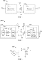
- FIG. 1 is a functional block diagram of an exemplary wireless power transfer system 100, which may be a loosely coupled wireless power system, in accordance with exemplary embodiments of the invention.
- Input power 102 may be provided to a transmitter 104 from a power source (not shown) for generating a field 105 for providing energy transfer.
- a receiver 108 may couple to the field 105 and generate output power 110 for storing or consumption by a device (not shown) coupled to the output power 110. Both the transmitter 104 and the receiver 108 are separated by a distance 112.
- transmitter 104 and receiver 108 are configured according to a mutual resonant relationship.
- the receiver 108 may receive power when the receiver 108 is located in an energy field 105 produced by the transmitter 104.
- the field 105 corresponds to a region where energy output by the transmitter 104 may be captured by a receiver 108. In some cases, the field 105 may correspond to the "near-field" of the transmitter 104 as will be further described below.
- the transmitter 104 may include a transmit antenna 114 for outputting an energy transmission.
- the receiver 108 further includes a receive antenna 118 for receiving or capturing energy from the energy transmission.
- the near-field may correspond to a region in which there are strong reactive fields resulting from the currents and charges in the transmit antenna 114 that minimally radiate power away from the transmit antenna 114.
- the near-field may correspond to a region that is within about one wavelength (or a fraction thereof) of the transmit antenna 114.
- the transmit and receive antennas 114 and 118 are sized according to applications and devices to be associated therewith. As described above, efficient energy transfer may occur by coupling a large portion of the energy in a field 105 of the transmit antenna 114 to a receive antenna 118 rather than propagating most of the energy in an electromagnetic wave to the far field. When positioned within the field 105, a "coupling mode" may be developed between the transmit antenna 114 and the receive antenna 118. The area around the transmit and receive antennas 114 and 118 where this coupling may occur is referred to herein as a coupling-mode region. In one embodiment, the transmit antenna 114 and the receive antenna 118 may communicate via a Bluetooth Low Energy (BLE) link.
- BLE Bluetooth Low Energy
- FIG. 2 is a functional block diagram of exemplary components that may be used in the wireless power transfer system 100 of FIG. 1 , in accordance with various exemplary embodiments of the invention.
- the transmitter 204 may include transmit circuitry 206 that may include an oscillator 222, a driver circuit 224, and a filter and matching circuit 226.
- the oscillator 222 may be configured to generate a signal at a desired frequency, such as 468.75 KHz, 6.78 MHz or 13.56 MHz, that may be adjusted in response to a frequency control signal 223.
- the oscillator signal may be provided to a driver circuit 224 configured to drive the transmit antenna 214 at, for example, a resonant frequency of the transmit antenna 214.
- the driver circuit 224 may be a switching amplifier configured to receive a square wave from the oscillator 222 and output a sine wave.
- the driver circuit 224 may be a class E amplifier.
- a filter and matching circuit 226 may be also included to filter out harmonics or other unwanted frequencies and match the impedance of the transmitter 204 to the transmit antenna 214.
- the transmitter 204 may wirelessly output power at a level sufficient for charging or power an electronic device.
- the power provided may be for example on the order of 300 milliWatts to 20 Watts to power or charge different devices with different power requirements. Higher or lower power levels may also be provided.
- the transmit antenna 214 and the receive antenna 218 may communicate via a Bluetooth Low Energy (BLE) link.
- BLE Bluetooth Low Energy
- the receiver 208 may include receive circuitry 210 that may include a matching circuit 232 and a rectifier and switching circuit 234 to generate a DC power output from an AC power input to charge a battery 236 as shown in FIG. 2 or to power a device (not shown) coupled to the receiver 108.
- the matching circuit 232 may be included to match the impedance of the receive circuitry 210 to the receive antenna 218.
- the receiver 208 and the transmitter 204 may additionally communicate on a separate communication channel 219 (e.g., Bluetooth, zigbee, cellular, etc).
- the receiver 208 and transmitter 204 may alternatively communicate via in-band signaling using characteristics of the wireless field 205.
- the receiver 208 may be configured to determine whether an amount of power transmitted by the transmitter 204 and receiver by the receiver 208 is appropriate for charging a battery 236. Further, the receiver 208 may be configured to enable a load (e.g., the battery 236) upon determining that the amount of power is appropriate. In some embodiments, the receiver 208 may be configured to directly utilize power received from a wireless power transfer field without charging of the battery 236.
- a selectively disablable associated load e.g., the battery 236
- the receiver 208 may be configured to determine whether an amount of power transmitted by the transmitter 204 and receiver by the receiver 208 is appropriate for charging a battery 236. Further, the receiver 208 may be configured to enable a load (e.g., the battery 236) upon determining that the amount of power is appropriate. In some embodiments, the receiver 208 may be configured to directly utilize power received from a wireless power transfer field without charging of the battery 236.
- a communication device such as a near-field communication (NFC) or radio-frequency identification device (RFID) may be configured to receive power from a wireless power transfer field and communicate by interacting with the wireless power transfer field and/or utilize the received power to communicate with the transmitter 204 or other devices.
- NFC near-field communication
- RFID radio-frequency identification device
- FIG. 3 is a schematic diagram of a portion of transmit circuitry 206 or receive circuitry 210 of FIG. 2 including a transmit or receive antenna 352, in accordance with exemplary embodiments of the invention.
- transmit or receive circuitry 350 used in exemplary embodiments including those described below may include an antenna 352 (or "loop" antenna).
- the antenna 352 may be configured to include an air core or a physical core such as a ferrite core (not shown). Air core loop antennas may be more tolerable to extraneous physical devices placed in the vicinity of the core.
- an air core loop antenna 352 allows the placement of other components within the core area.
- an air core loop may more readily enable placement of the receive antenna 218 ( FIG.
- the antenna 352 may be a coil (e.g., an induction coil) and/or an RF antenna, or any other suitable device to wirelessly receive or output power.
- the antenna 352 may be implemented with a Litz wire or as an antenna strip designed for low resistance.
- the antenna 352 may not need "turns" to be of a practical dimension.
- An exemplary implementation of the antenna 352 may be "electrically small” (e.g., a fraction of the wavelength) and tuned to resonate at a usable low frequency by using capacitors to define the resonant frequency.
- efficient transfer of energy between the transmitter 104 and receiver 108 may occur during matched or nearly matched resonance between the transmitter 104 and the receiver 108. However, even when resonance between the transmitter 104 and receiver 108 are not matched, energy may be transferred, although the efficiency may be affected. Transfer of energy occurs by coupling energy from the field 105 of the transmit antenna 214 coil to the receive antenna 218 residing in the neighborhood where this field 105 is established rather than propagating the energy from the transmit antenna 214 into free space.
- the resonant frequency of the loop or magnetic antennas is based on the inductance and capacitance.
- Inductance may be simply the inductance created by the antenna 352, whereas, capacitance may be added to the antenna's inductance to create a resonant structure at a desired resonant frequency.
- the capacitor 354 and the capacitor 356 may be added to the transmit or receive circuitry 350 to create a resonant circuit that selects a signal 358 at a resonant frequency. Accordingly, for larger diameter antennas, the size of capacitance needed to sustain resonance may decrease as the diameter or inductance of the loop increases. Furthermore, as the diameter of the antenna increases, the efficient energy transfer area of the near-field may increase.
- resonant circuits formed using other components are also possible.
- a capacitor may be placed in parallel between the two terminals of the antenna 352.
- a signal 358 with a frequency that substantially corresponds to the resonant frequency of the antenna 352 may be an input to the antenna 352.
- the transmitter 104 may be configured to output a time varying magnetic field with a frequency corresponding to the resonant frequency of the transmit antenna 114.
- the time varying magnetic field may induce a current in the receive antenna 118.
- the AC signal induced in the receive antenna 118 may be rectified as described above to produce a DC signal that may be provided to charge or to power a load.
- FIG. 4 illustrates a wireless power system 480 including a power transfer unit "PTU” 404 (e.g., a power transfer unit that provides wireless charging) and one or more power receive units “PRUs” 484 (e.g., power receive units that are wirelessly chargeable devices), according to an exemplary embodiment of the invention.
- the PTU 404 may create a magnetic field which couples to the PRU 484.
- the PRU 484 may convert magnetic energy received from the PTU 404 into electrical energy.
- the PRUs 484 may include devices such as cellular phones, portable music players, computers, laptop computers, tablet computers, computer peripheral devices, communication devices (e.g., Bluetooth headsets), digital cameras, hearing aids (and other medical devices), etc.
- the PRU 484 may be connected to a device to be charged which draws on the electrical energy.
- the device to be charged may be integrated into the PRU 484.
- the PRU 484 may be placed on the PTU 404 for the purpose of charging the PRU 484.
- the PTU 404 and the PRU 484 may communicate via a Bluetooth Low Energy (BLE) link.
- BLE Bluetooth Low Energy
- the wireless power system 480 includes a non-compliant object 486 (or "non-compliant device,” “foreign object,” or “foreign device”), which may comprise a non-compliant device or component.
- the non-compliant object 486 may include a damaged device, a device not built to the correct specifications (e.g., not in compliance with a charging standard or any other object made of electrically conductive material that couples to the magnetic field (e.g., jewelry, eye-glasses, key-chains, etc.).
- the non-compliant object 486 may be any object or device that is unable to communicate with the PTU 404 and function with a system control algorithm, which allows the PTU 404 no method to regulate or detect the electrical energy consumed by the non-compliant object 486. Since the PTU 404 creates a magnetic field, electrical energy may be transferred to any device or object that couples to the PTU 404 magnetic field.
- the non-compliant object 486 and each of the one or more PRUs 484 may be positioned within, near, or around a charging region of the PTU 404, which may cause the PRUs 484 to couple to the PTU 404 magnetic field and absorb electrical energy.
- the non-compliant object may affect the consumption of power transmitted by the PTU 404 and/or affect the charging region when it is within, near, or around the charging region.
- the energy absorbed may be dissipated as heat, which may damage the non-compliant object 486, harm or burn the user, cause a fire, damage the PTU 404, or create any other safety issue.
- the PTU 404 may continue to transfer power to the non-compliant object 486 indefinitely.
- the PTU 404 may be configured to detect the non-compliant object 486, as described below.
- the PTU 404 may be configured to detect, according to one or more methods, one or more of the non-compliant objects 486 affecting an associated charging region.
- the PTU 404 may detect the non-compliant object 486 using a method based on system measurements taken on both the PTU 404 and the one or more PRU 484.
- the PTU 404 may sample the current and voltage at both the PTU 404 coil or power amplifier (PA) supply (e.g., driver circuit 724, see FIG. 7 ) and the PRU 484 rectifier output (e.g., output of the RF-to-DC converter 820, see FIG. 8 ).
- PA power amplifier
- the PTU 404 calculates the instantaneous power based on the current and voltage measurements at the sampled times at both the PTU 404 coil or PA supply and the rectifier output of the one or more PRU 484. The PTU 404 may then compare the two readings and assess if the difference between the two readings is justified by the parasitic losses in the system or if it is excessive (e.g., exceeds a threshold), thus indicating the presence of non-compliant object 486.
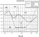
- FIG. 4B is a graph of voltage 450 and current 455 measurements of a PRU load over time.
- the instantaneous power 460 absorbed by the load is the product of the instantaneous voltage 450 and current 455: as their values change dynamically, using the sampled values (e.g., sampled instantaneous power values 470) to determine the average power 475 absorbed may lead to erroneous conclusions.
- these values 470 may not accurately capture average power between sample times because the power values of the load may have significant fluctuations. The information therefore may not capture the dynamic behavior of the load unless the sampling frequency is very high, which may be impractical due to increased processing time and cost of implementation.
- Low-pass filters, which average the instantaneous values may help improve the measurements, but do not accurately capture the instantaneous product of current and voltage, and may require relatively large time constants, which are not easily integrateable.
- the PTU 404 may measure the integral of the power during the entire sampled time at both the PTU 404 and the PRU 484 (which is equivalent to the average power during the sampled period times the sampled period duration).
- the integral of the power represents the energy (e.g., total power over a period of time) at both the PTU 404 and the PRU 484.
- FIG. 4B also shows the integral of the power of the load over the time T0-T4 as the shaded area 475. Measuring the energy, instead of the power, at both the PTU 404 and the PRU 484 has several advantages.
- the energy more accurately measures the total power at both the PTU 404 and the PRU 484 over a period of time and thus may more accurately detect the presence of the non-compliant object 486, as the measurement is less subject to random noise and instantaneous variation of the load.
- Such accuracy may be particularly important when integrating over a longer period of time and/or large energy transfer.
- the PTU 404 may have to detect a relatively small amount of lost power (e.g., 1W) compared to the total power measured over the sampled period of time (e.g, 50W). Therefore, it may be desirable to have the energy measurements be accurate over a relatively large dynamic range.
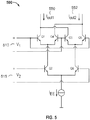
- FIG. 5 is a diagram of an exemplary Gilbert multiplier cell 500 in accordance with embodiments described herein.
- the Gilbert cell 500 consists of two differential amplifier stages formed by emitter-coupled transistor pairs (Q1/Q4, Q3/Q5) whose outputs are connected (currents summed) with opposite phases at I out1 550 and I out2 552, respectively.
- the emitter junctions of these amplifier stages are fed by the collectors of a third differential pair (Q2/Q6).
- the output currents of Q2/Q6 become emitter currents for the differential amplifiers.
- the output currents I out1 550 and I out2 552 are a 4 quadrant multiplication of the differential base voltages of the V 1 510 and V 2 515 inputs.
- the capacitive integrator may be periodically sampled to an analog-to-digital (A/D) converter and reset to start a new period.
- FIG. 6 is a diagram of an exemplary integrator 600 in accordance with embodiments described herein.
- the integrator 600 comprises an analog block 601 and a digital block 650.
- the differential analog signal at the output of the multiplier e.g., Gilbert multiplier cell 500 of FIG. 5
- V/F differential voltage-to-frequency
- the analog block 601 generates output frequencies f 1 620 and f 2 625 from the voltages V O and V REF and ring oscillators 610 and 615.
- the output frequencies f 1 620 and f 2 625 are then sent to the digital block 650.
- the output frequencies 620 and 625 are then integrated by counters 655; the difference of the integrals is used to generate the measured value of energy D e .
- a non-limiting benefit of the digital integrator 600 is the ability to calibrate out a possible offset at the analog block 601. By measuring the output frequency with a zero input signal and then subtracting the reading from the previous measurement (or at predetermined times), the integrator 600 may calibrate out a possible offset in the analog measurements of voltages and currents. Misalignment in time between the PTU 404 and PRU 484 measurements occur because there is no real time clock in the wireless power transfer system 100 and therefore it may be difficult to synchronize the measurements at the PTU 404 and PRU 484.
- An additional benefit of the proposed implementation is that, since the integration time must be long (e.g., >10x) compared to a possible sampling misalignment between the PTU 404 and the PRU 484, the effect of any non-synchronized measurements may be minimized.
- the Gilbert multiplier cell 500 may be connected to the integrator 600 to compute the energy measurement (e.g., integral of the product of current and voltage.)
- a resistive load on the Gilbert multiplier cell 500 may provide a voltage to be fed to the integrator 600.
- the Gilbert multiplier cell 500 may be inverted in polarity, so that the current output directly feeds the ring oscillators 610 and 615 of the integrator 600.
- the combination of a multiplier and an integrator to determine the integral of the product of current and voltage to determine, at least in part, the energy measurement may be included in the PTU 404 and/or the PRU 484.
- the PTU 404 may comprise a wireless power transmitter (e.g., the transmitter 104 of FIG. 1 ) that may transmit power to the PRU 484 within, near, or around an associated charging region.
- the PTU 404 may be configured to determine whether or not said transmitted energy is unaccounted for (e.g., if the non-compliant object 486 is consuming energy).
- the PTU 404 may be configured to further determine whether the non-compliant object 486 is consuming energy greater than a specified threshold.
- the specified threshold may be a fixed value, or it may be dynamically changed based on various specifications of the system components (e.g., a system operating point changing its output energy, a dynamic load demanding a variable amount of energy, etc.), as further described below.
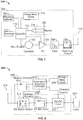
- FIG. 7 is a functional block diagram of a PTU 704 (such as the PTU 404) that may be used in the wireless power transfer system of FIG. 1 , in accordance with exemplary embodiments of the invention.
- the PTU 704 may receive power through a number of power sources, e.g., an AC-DC converter (not shown) to convert conventional AC power present in a building, a DC-DC converter (not shown) to convert a conventional DC power source to a voltage suitable for the PTU 704, or directly from a conventional DC power source (not shown).
- an AC-DC converter not shown
- DC-DC converter not shown
- FIG. 7 is a functional block diagram of a PTU 704 (such as the PTU 404) that may be used in the wireless power transfer system of FIG. 1 , in accordance with exemplary embodiments of the invention.
- the PTU 704 may receive power through a number of power sources, e.g., an AC-DC converter (not shown) to convert conventional AC power present in a building,
- the PTU 704 may include a transmit antenna 714 for generating an electromagnetic or magnetic field, hereinafter referred to as a "charging region.”
- the transmit antenna 714 may be a coil (e.g., an induction coil) and/or an RF antenna, or any other suitable device to wirelessly output power.
- the transmit antenna 714 may be implemented with a Litz wire or as an antenna strip designed for low resistance.
- the transmit antenna 714 may be associated with a larger structure, such as a table, mat, lamp, or other stationary configuration. Accordingly, the transmit antenna 714 may not need "turns" to be of a practical dimension.
- An exemplary implementation of the transmit antenna 714 may be "electrically small” (e.g., a fraction of the wavelength) and tuned to resonate at a usable low frequency by using capacitors (e.g., the capacitors 354 and 356 of FIG. 3 ) to define the resonant frequency.
- the transmit antenna 714 (or another antenna) may transmit power to a receiver device (e.g., the PRU 484) within, near, or around the charging region.
- the transmit antenna 714 (or another antenna) may receive an acknowledgement from the PRU 484 regarding the amount of power it has received, as described in connection with FIG. 4 .
- the transmit antenna 714 may also receive information from the PRU 484 about the various specifications of the PRU 484, as described below.
- the transmit antenna 714 (or another antenna) may also receive confirmation from the PRU 484 that the PRU 484 is fully charged.
- the transmit antenna 714 (or another antenna) may communicate with the PRU 484 via a Bluetooth Low Energy (BLE) link.
- BLE Bluetooth Low Energy
- the PTU 704 may not remain on indefinitely. This prevents the PTU 704 from running long after the PRUs 484 in its perimeter are fully charged, which may occur if the transmit antenna 714 fails to receive or receives a faulty confirmation from the PRU 484 when it is fully charged.
- a user may program the PTU 704 to shut off after a desired amount of time. To prevent the PTU 704 from automatically shutting down if another PRU 484 is placed in its perimeter, the PTU 704 may shut off automatically after a set period of lack of motion detected in its perimeter, as described below.
- the user may be able to set the inactivity time interval and change it as desired. As a non-limiting example, the time interval may be longer than that needed to fully charge the PRU 484 under the assumption that the PRU 484 is initially fully discharged.
- the PTU 704 may further include transmit circuitry 706.
- the transmit circuitry 706 may include an oscillator 723 for generating oscillating signals (e.g., RF signals).
- the transmit circuitry 706 may provide RF power to the transmit antenna 714 via the RF signals, resulting in generation of energy (e.g., magnetic flux) about the transmit antenna 714.
- the PTU 704 may operate at any suitable frequency, e.g., the 6.78 MHz ISM band.
- the transmit circuitry 706 may include a fixed impedance matching circuit 709 for matching the impedance of the transmit circuitry 706 (e.g., 50 ohms) to the transmit antenna 714.
- the transmit circuitry 706 may also include a low pass filter (LPF) 708 configured to reduce harmonic emissions to levels that prevent self-jamming of the PRUs 484.
- LPF low pass filter
- Other exemplary embodiments may include different filter topologies, such as notch filters that attenuate specific frequencies while passing others.
- the transmit circuitry 706 may further include a driver circuit 724 configured to drive the RF signals.
- Other exemplary embodiments may include an adaptive impedance match that may be varied based on measurable transmit metrics, such as output power to the transmit antenna 714 or DC current to the driver circuit 724.
- the transmit circuitry 706 may further comprise discrete devices, discrete circuits, and/or an integrated assembly of components.
- An exemplary RF power output from the transmit antenna 714 may be from 0.3 watts to 20 watts or may also be a higher or lower value.
- the transmit circuitry 706 may further include a controller 715 for, among other functions, selectively enabling the oscillator 723 during transmit phases (or duty cycles) of the PRUs 484.
- the controller 715 may also adjust the frequency or phase of the oscillator 723. Adjusting the phase of the oscillator 723 and related circuitry in the transmission path may allow for reduction of out-of-band emissions, especially when transitioning from one frequency to another.
- the controller 715 may also adjust the output power level of the oscillator 723 to implement a communication protocol for interacting with the PRUs 484.
- the controller 715 may also perform calculations based on data it sends and receives from other components in the transmit circuitry 706.
- the transmit circuitry 706 may also include a memory 770 for temporarily or permanently storing data.
- the memory 770 may also store various specifications of the components of the PTU 704 and/or the PRUs 484 for use in calculations as described below.
- the controller 715 may gather and track information about the whereabouts and status of the PRUs 484 that may be associated with the PTU 704.
- the transmit circuitry 706 may include a presence detector 780 (e.g., a motion detector) to detect the initial presence of the PRU 484 to be charged when the PRU 484 enters the charging region and to turn on the PTU 704 in such an event.
- the presence detector 780 may detect the PRU 484 via the transmit antenna 714 or another appropriate antenna not shown in FIG. 7 .
- the controller 715 may adjust the amount of power going to or from the driver circuit 724 in response to presence signals from the presence detector 780.
- the transmit antenna 714 may then transfer RF power to the PRU 484.
- the transmit circuitry 706 may further include a load sensing circuit 716 for monitoring the current flowing to the driver circuit 724, which may be affected by the presence or absence of the PRUs 484 or a non-compliant device (e.g., the non-compliant object 486 of FIG. 4 ) in the vicinity of the charging region as detected by the presence detector 780.
- the controller 715 may also detect load changes on the driver circuit 724 to determine whether to enable the oscillator 723.
- the transmit circuitry 706 may further include an energy measurement circuit 775. As shown in FIG. 7 , the energy measurement circuit 775 is coupled to the controller 715. In other embodiments, the energy measurement circuit 775 may comprise a component of the controller 715. The energy measurement circuit 775 may be used to detect the presence of the non-compliant object 486 affecting the charging region. In some embodiments, the energy measurement circuit 775 may comprise the Gilbert multiplier cell 500 of FIG. 5 and/or the integrator 600 of FIG. 6 . The energy measurement circuit 775 may determine whether and to what extent the power or energy transmitted via the transmit antenna 714 is unaccounted for (e.g., determine the amount of lost power or energy). As described above with respect to FIGs.
- the energy measurement circuit 775 may compare the energy (e.g., the integral of the product of current and voltage) transferred by the PTU 404 or PTU 704 with the energy absorbed by the PRU 484 over the approximately same time period.
- the time period may comprise a fraction of a second (e.g., 250-500ms).
- the period of time may be a smaller fraction of time (e.g., 10ms, 25ms, 50 ms, 100ms, etc.) or a greater fraction of time (500ms, lsec, 2 secs, etc.)
- the time period may comprise a period of time that is greater than the sampling intervals (e.g., greater than 1x, 2x, 5x, 10x, etc.).
- the PRU 484 may send the energy absorbed to the PTU 404 and/or PTU 704 via a BLE link or other communication link.
- the PRU 484 may send data relating to the energy absorbed (e.g., current, voltage, etc.) to the PTU 404 and/or PTU 704 for the PTU 404 and/or PTU 704 to determine the amount of energy absorbed at the PRU 484 over the period of time.
- the PTU 704 may receive a message from each PRU 484 indicating the energy absorbed by the corresponding PRU 484. The energy measurement circuit 775 may then compare the sum of the energy absorbed from each PRU 484 with the total energy transferred by the PTU 704.
- energy measurement circuit 775 may determine that the difference between the energy transferred and the energy absorbed exceeds a threshold. If so, the energy measurement circuit 775 may then determine that the non-compliant object 486 is present. The energy measurement circuit 775 or controller 715 may then turn off the power to the PTU 704. In another embodiment, rather than simply turning off the PTU 704, the energy measurement circuit 775 or controller 715 may instead or additionally adjust the power level and/or change a state of transmission of power from the PTU 704 to the PRU 484. In some embodiments, the above functions of the energy measurement circuit 775 may be performed by the controller 715. In these embodiments, the energy measurement circuit 775 may be excluded from the transmit circuitry 706.
- FIG. 8 is a functional block diagram of the PRU 484 (as in FIG. 4 ) that may be used in the wireless power transfer system of FIG. 1 , in accordance with exemplary embodiments of the invention.
- the PRU 484 may include receive circuitry 810 comprising the various components of the PRU 484.
- the receive circuitry 810 may include a receive antenna 818 for receiving power from a transmit antenna (e.g., the transmit antenna 714 of FIG. 7 ).
- the PRU 484 may further couple to a load 850 for providing received power thereto.
- the load 850 may be external to the PRU 484, or the load 850 may be integrated into the PRU 484 (not shown).
- the receive circuitry 810 may further include a processor 816 for coordinating the processes of the PRU 484, as described below.
- the receive circuitry 810 may further include an energy measurement circuit 875. As shown in FIG. 8 , the energy measurement circuit 875 is coupled to the processor 816. In other embodiments, the energy measurement circuit 875 may comprise a component of the processor 816.
- the receive antenna 818 may be tuned to resonate at a similar frequency, or within a specified range of frequencies, as the transmit antenna 714 ( FIG. 7 ).
- the receive antenna 818 may be similarly dimensioned with the transmit antenna 714 or it may be differently sized based on the dimensions of the load 850.
- the receive antenna 818 may communicate with the transmit antenna 714 via a Bluetooth Low Energy (BLE) link. This communication may allow the PRU 484 to send feedback data to the PTU 704, which may allow the PTU 704 to vary the strength of its magnetic field to adjust the electrical energy being transferred to the PRU 484.
- BLE Bluetooth Low Energy
- the receive antenna 818 may be implemented as a multi-turn coil to reduce the capacitance value of a tuning capacitor (not shown) and increase the receive coil's impedance.
- the receive antenna 818 may be placed around the substantial circumference of the load 850 in order to maximize the antenna diameter and reduce the number of loop turns (e.g., windings) of the receive antenna 818 and the inter-winding capacitance.
- the energy from the transmit antenna 714 may be propagated wirelessly to the receive antenna 818 and then coupled through the rest of the receive circuitry 810 to the load 850.
- the energy measurement circuit 875 may comprise the Gilbert multiplier cell 500 of FIG. 5 and/or the integrator 600 of FIG. 6 .
- the energy measurement circuit 875 may determine the power or energy received from the transmit antenna 714 via the receive antenna 818.
- the energy measurement circuit 875 may determine the energy (e.g., the integral of the product of current and voltage) absorbed by the PRU 484 over the approximately same time period as the energy measurement circuit 775 of the PTU 404 and/or PTU 704 of FIG.
- the PRU 484 may send the determined energy absorbed via the receive antenna 818 to the PTU 404 and/or PTU 704 via a BLE link or other communication link.
- the PRU 484 may send energy data (e.g., voltage, current, etc.) to the PTU 404 and/or PTU 704 for the PTU 404 and/or PTU 704 to determine the energy absorbed at the PRU 484.
- each PRU 484 may transmit to the PTU 404 and/or PTU 704 the energy absorbed by the corresponding PRU 484.
- the controller 715 and/or the energy measurement circuit 875 of the PTU 404 and/or PTU 704 may then detect the presence of the non-compliant object 486 based at least in part on the energy measurements from the one or more PRUs 484.
- the receive circuitry 810 may provide an impedance match to the receive antenna 818.
- the receive circuitry 810 may include power conversion circuitry 806 for converting a received RF energy source into charging power for use by the load 850.
- the power conversion circuitry 806 may include an RF-to-DC converter 820 to rectify the RF energy signal received at the receive antenna 818 into a non-alternating power with an output voltage.
- the RF-to-DC converter 820 may be a partial or full rectifier, a regulator, a bridge, a doubler, a linear or switching converter, etc.
- the power conversion circuitry 806 may also include a DC-to-DC converter 822 (or other power regulator) to convert the rectified RF energy signal into an energy potential (e.g., voltage) that is compatible with the load 850.
- a DC-to-DC converter 822 or other power regulator to convert the rectified RF energy signal into an energy potential (e.g., voltage) that is compatible with the load 850.
- the receive circuitry 810 may further include switching circuitry 812 for connecting or disconnecting the receive antenna 818 to or from the power conversion circuitry 806. Disconnecting the receive antenna 818 from the power conversion circuitry 806 may suspend charging of the load 850 and/or change the "load” 850 as "seen" by the PTU 704.
- the PTU 704 may require the PRU 484 to conduct a "calibration" procedure as follows.
- a “step” in the PRU 484 power absorption can be generated, which is added to the existing load. This step can be implemented, for example, by switching a resistive load either at the output of the DC-DC converter 822 or at the rectified output.
- a new measurement is conducted by both the PRU 484 and the PTU 704. Assuming that no other change occurs in the overall power delivery system, the PTU 704 and the PRU 484 may record a "delta" or change in power relative to prior measurements.
- This calibration method may not account for an additional component of loss: the induced heat in the PRU 484 metal components and other losses generated by the mere presence of the PRU 484 on the PTU 704. Such losses may be assessed by another procedure: when the PRU 484 is placed on the PTU 704, and prior to the PRU 484 absorbing power, the PTU 704 may record the change in overall power absorption and associated with the PRU 484 as a fixed (not measured by the PRU 484) loss. If multiple PRU's 484 are placed on the PTU 704 at the same time, or other power absorbing objects are placed at the same time the change in overall power absorption measurement may not be account for PRU's 484.
- One possible way of managing such inaccuracies may be implemented by the PRU 484 providing an "estimate" of such losses during a "login” process. This method may require that the manufacturer of the PRU 484 store in a register the typical power loss associated with placing the PRU 484 on a master PTU 704. The PTU 704 manufacturer may then optionally adjust this information based on his knowledge of how its PTUs 704 compare to the master PTU 704. This approach may improve the error associated with a lost power algorithm.
- the processor 816 may be configured to time-multiplex (e.g., switch) the loading and unloading of one or more PRUs 484 to enable other PRUs 484 to more efficiently couple to the PTU 704.
- Unloading of the PRU 484 (hereinafter referred to as “cloaking” or “cloaked") may eliminate coupling to other nearby PRUs 484 or reduce loading on nearby PTUs 704. Cloaking may also occur upon the occurrence of other events, e.g., detection of an external wired charging source (e.g., wall/USB power) providing charging power to the load 850. The switching between unloading and loading may be detected by the PTU 704.
- an external wired charging source e.g., wall/USB power
- the switching between unloading and loading may be performed at a particular speed to function as a protocol that enables the sending of a message from the PRU 484 to the PTU 704.
- the switching speed may be on the order of 100 ⁇ sec.
- the PRU 484 may be configured to send various specifications about the PRU 484 to the PTU 704, e.g., specifications for the PTU 704 to calculate the difference in energy between the PTU 704 and the PRU 484.
- communication between the PTU 704 and the PRU 484 refers to a device sensing and charging control mechanism, rather than conventional two-way communication (e.g., in band signaling using the coupling field).
- the PTU 704 may use on/off keying of the transmitted signal to adjust whether energy is available in the near-field.
- the PRU 484 may interpret these changes in energy as a message from the PTU 704.
- the PRU 484 may use tuning and de-tuning of the receive antenna 818 to adjust how much power is being accepted from the field. In some cases, the tuning and de-tuning may be accomplished via the switching circuitry 812.
- the PTU 704 may detect this difference in power used from the field and interpret these changes as a message from the PRU 484.
- Other forms of modulation of the transmit power and the load 850 behavior may be utilized.
- the receive circuitry 810 may further include signaling and beacon detector circuitry 814 to identify received energy fluctuations that may be informational signaling from the PTU 704 to the PRU 484.
- the processor 816 may monitor the signaling and beacon detector circuitry to determine a beacon state and extract messages sent from the PTU 704.
- the signaling and beacon detector circuitry 814 may be used to detect the transmission of a reduced RF signal energy (e.g., a beacon signal).
- the signaling and beacon detector circuitry 814 may further rectify the reduced RF signal energy into a nominal power for awakening either un-powered or power-depleted circuits within receive circuitry 810 in order to configure receive circuitry 810 for wireless charging.
- FIG. 9 illustrates a flowchart 900 of an exemplary method for the controller 715 (of FIG. 7 ) to determine whether a non-compliant object (e.g., the non-compliant object or the non-compliant device 486) is affecting the charging region (as described above in regards to FIG. 7 ).
- the controller 715 begins the method when the PTU 704 is charging one or more PRUs (e.g., the PRUs 484).
- the controller 715 determines the energy transferred by the PTU 704 over a period of time.
- the controller receives from the PRUs 484 the energy absorbed by each PRU 484 over approximately the same period of time.
- the controller 715 can determine the energy transferred, and the PRU 484 can determine the energy absorbed, at least in part, by computing the integral of the current and power of the PTU 704 or PRU 484, respectively, as described above with respect to FIGs. 5 and 6 .
- the controller 715 compares the total energy transferred by the PTU 704 with the sum of the energy absorbed from each PRU 484 and determines whether the difference satisfies a threshold for acceptable energy loss. If not, then the controller 715 continues charging the PRUs 484 in block 916 and then returns to block 904. If the difference does exceed the threshold, then at block 910, the controller 715 determines that the non-compliant object 486 is present.
- a protective action may comprise the controller 715 turning off the power to the PTU 704.
- the PTU 704 may instead or additionally adjust the power level and/or change a state of transmission of power from the PTU 704 to the PRU 484. The method ends at block 914.
- any suitable means capable of performing the operations such as various hardware and/or software component(s), circuits, and/or module(s).
- any operations illustrated in the Figures may be performed by corresponding functional means capable of performing the operations.
- means for transmitting power may comprise the transmit antenna 114, 214, 714 or the transmit or receive antenna 352 of FIGs. 1, 2 , 7 , and 3 above, respectively.
- means for receiving from the one or more chargeable devices a measurement of a first amount of energy received by the one or more chargeable devices over a first period of time may comprise the receive antenna 118, 218, 818 or the transmit or receive antenna 352 of FIGs. 1, 2 , 8 , and 3 above, respectively.
- means for measuring a second amount of energy provided by the transmitting means over a second period of time may comprise the controller 715 or energy measurement circuit 775 of FIG. 7 .
- means for determining whether an object other than the one or more chargeable devices is absorbing power may comprise the controller 715 or energy measurement circuit 775 of FIG. 7 .
- Information and signals may be represented using any of a variety of different technologies and techniques.
- data, instructions, commands, information, signals, bits, symbols, and chips that may be referenced throughout the above description may be represented by voltages, currents, electromagnetic waves, magnetic fields or particles, optical fields or particles, or any combination thereof.
- DSP Digital Signal Processor
- ASIC Application Specific Integrated Circuit
- FPGA Field Programmable Gate Array
- a general purpose processor may be a microprocessor, but in the alternative, the processor may be any conventional processor, controller, microcontroller, or state machine.
- a processor may also be implemented as a combination of computing devices, e.g., a combination of a DSP and a microprocessor, a plurality of microprocessors, one or more microprocessors in conjunction with a DSP core, or any other such configuration.
- a software module may reside in Random Access Memory (RAM), flash memory, Read Only Memory (ROM), Electrically Programmable ROM (EPROM), Electrically Erasable Programmable ROM (EEPROM), registers, hard disk, a removable disk, a CD ROM, or any other form of storage medium known in the art.
- RAM Random Access Memory
- ROM Read Only Memory
- EPROM Electrically Programmable ROM
- EEPROM Electrically Erasable Programmable ROM
- registers hard disk, a removable disk, a CD ROM, or any other form of storage medium known in the art.
- a storage medium is coupled to the processor such that the processor may read information from, and write information to, the storage medium.
- Disk and disc includes compact disc (CD), laser disc, optical disc, digital versatile disc (DVD), floppy disk and blu ray disc where disks usually reproduce data magnetically, while discs reproduce data optically with lasers. Combinations of the above may also be included within the scope of computer readable media.
- the processor and the storage medium may reside in an ASIC.
Landscapes
- Engineering & Computer Science (AREA)
- Computer Networks & Wireless Communication (AREA)
- Power Engineering (AREA)
- Signal Processing (AREA)
- Charge And Discharge Circuits For Batteries Or The Like (AREA)
Description
- The described technology generally relates to wireless power. More specifically, the disclosure is directed to devices, systems, and methods related to detection of non-compliant objects present in a magnetic field.
- Loosely coupled wireless power systems include a power transfer unit (e.g., a charging device) and one or more power receive units (e.g., a cellphone, a laptop, etc.) to be charged. When non-compliant objects are present within, near, or around the charging region of the power transfer unit, electrical energy may be lost in the wireless power system. The lost electrical energy may harm a user, damage a device or object, start a fire, etc. As such, it is desirable to detect when the power system experiences a loss in power and to respond appropriately.
-
EP 2 779 359 A2 discloses an apparatus and a method for detecting foreign objects in a wireless power transmitting system are disclosed. The wireless power transmitting apparatus or the wireless power receiving apparatus determines whether a foreign object is detected prior to initial charging (S205). When a foreign object is detected, the wireless power transmitting apparatus or the wireless power receiving apparatus performs a power limit operation in response to the detection of the foreign object (S225). If a foreign object is not detected prior to the initial charging, the wireless power transmitting apparatus or the wireless power receiving apparatus performs an operation of foreign object detection during charging, after charging starts (S210). If a foreign object is not detected during charging, a problem may arise in power transmission due to a fine foreign object which has not been detected, and thus, the wireless power transmitting apparatus of the wireless power receiving apparatus limits power based on a temperature sensor (S220).US2013/062959 A1 discloses embodiments are directed to detecting and identifying a type of a wireless power device in a wireless power transfer field. According to one aspect, systems and methods are disclosed which describe limiting power transfer to non-compliant devices and detection of undesired power absorbers, such as metal objects, in a wireless power system. A method may include detecting one or more non-compliant devices and/or undesired wireless power absorbers positioned within a charging region of a wireless power transmitter. The method may further include limiting an amount of power transmitted by a transmitter in response to the detection, or reducing the amount of power received by the non-compliant device.
WO2014/060871 A1 discloses a power transmitter (101) transfers power to a power receiver (105) using a wireless power signal. The power transmitter (101) comprises an inductor (103) driven by a power signal generator (201) to provide the power signal. A calibration controller (211) determines whether a power loss calibration has been performed for the power transmitter (101) and power receiver (105) pairing. The calibration adapts an expected relationship between a received power indication provided by the power receiver (105) and a transmitted power indication for the power transmitter (101). A power limiter (205) restricts the power provided to the inductor to not exceed a threshold unless a power loss calibration has been performed for the pairing. The expected relationship may be used to detect unaccounted for power losses, e.g. due to foreign objects being present. The calibrated expected relationship may provide improved accuracy allowing accurate detection at higher power levels. At lower power levels such accuracy is not needed, and no calibration needs to be performed. - Various embodiments of systems, methods and devices within the scope of the appended claims each have several aspects, no single one of which is solely responsible for the desirable attributes described herein. Without limiting the scope of the appended claims, some prominent features are described herein.
- Details of one or more embodiments of the subject matter described in this specification are set forth in the accompanying drawings and the description below. Other features, aspects, and advantages will become apparent from the description, the drawings, and the claims. Note that the relative dimensions of the following figures may not be drawn to scale.
- One aspect of the disclosure provides an apparatus for wirelessly transferring power. The apparatus includes an antenna configured to provide wireless power to a chargeable device sufficient to charge or power the chargeable device positioned within a charging region of the antenna. The apparatus further includes a receiver configured to receive from the chargeable device a measurement of a first amount of energy received by the chargeable device over a first period of time. The apparatus further includes a processor configured to measure a second amount of energy provided by the antenna over a second period of time. The processor further configured to compare the first amount of energy received from the chargeable device to the second amount of energy over the second period. The processor further configured to determine whether an object other than the chargeable device is absorbing power provided via the antenna based at least in part on comparing the first amount of energy and the second amount of energy.
- Another aspect of the disclosure provides a method for wirelessly transferring power. The method includes transmitting power from a transmitter at a power level sufficient to power or charge one or more chargeable devices positioned within a charging region. The method further includes receiving from the one or more chargeable devices a measurement of a first amount of energy received by the chargeable devices over a first period of time. The method further includes measuring a second amount of energy provided by the transmitter over a second period of time. The method further includes comparing the first amount of energy received from the chargeable devices to the second amount of energy provided by the transmitter over the second period. The method further includes determining whether an object other than the chargeable device is absorbing power provided via the transmitter based at least in part on comparing the first amount and the second amount of energy.
- Another aspect of the disclosure provides an apparatus for wirelessly transferring power. The apparatus includes means for transmitting power at a power level sufficient to power or charge one or more chargeable devices positioned within a charging region. The apparatus further includes means for receiving from the one or more chargeable devices a measurement of a first amount of energy received by the one or more chargeable devices over a first period of time. The apparatus further includes means for measuring a second amount of energy provided by the transmitting means over a second period of time. The apparatus further includes comparing the first amount of energy received from the one or more chargeable devices to the second amount of energy provided by the transmitting means over the second period. The apparatus further includes means for determining whether an object other than the one or more chargeable devices is absorbing power provided via the transmitting means based at least in part on comparing the first amount and the second amount of energy.
- Another aspect of the disclosure provides a non-transitory computer readable medium. The medium comprising instructions that when executed cause a processor to perform a method of transmitting power from a transmitter at a power level sufficient to power or charge one or more chargeable devices positioned within a charging region. The medium further comprising instructions that when executed cause a processor to perform a method of receiving from the one or more chargeable devices a measurement of a first amount of energy received by the one or more chargeable devices over a first period of time. The medium further comprising instructions that when executed cause a processor to perform a method of measuring a second amount of energy provided by the transmitter over a second period of time. The medium further comprising instructions that when executed cause a processor to perform a method of comparing the first amount of energy received from the one or more chargeable devices to the second amount of energy provided by the transmitter over the second period. The medium further comprising instructions that when executed cause a processor to perform a method of determining whether an object other than the one or more chargeable devices is absorbing power provided via the transmitter based at least in part on comparing the first amount and the second amount of energy.
- Another aspect of the disclosure provides an apparatus for wirelessly receiving power. The apparatus includes an antenna configured to receive wireless power from a wireless power transmitter. The apparatus further includes a processor configured to determine an amount of energy received by the antenna over a period of time. The apparatus further includes a transmitter configured to transmit the measurement of the amount of energy received by the antenna over the period of time.
- Another aspect of the disclosure provides a method for wirelessly receiving power. The method includes wirelessly receiving power from a wireless power transmitter. The method further determining an amount of energy received by the antenna over a period of time. The apparatus further includes transmitting the determined amount of energy received by the antenna over the period of time.
-
-
FIG. 1 is a functional block diagram of an exemplary wireless power transfer system, in accordance with exemplary embodiments of the invention. -
FIG. 2 is a functional block diagram of exemplary components that may be used in the wireless power transfer system ofFIG. 1 , in accordance with various exemplary embodiments of the invention. -
FIG. 3 is a schematic diagram of a portion of transmit circuitry or receive circuitry ofFIG. 2 including a transmit or receive antenna, in accordance with exemplary embodiments of the invention. -
FIG. 4A illustrates a wireless power system including a wireless power transmitter and receivers, according to an exemplary embodiment of the invention. -
FIG. 4B is a graph of voltage, current, and power measurements of an exemplary load. -
FIG. 5 is a diagram of an exemplary Gilbert multiplier cell. -
FIG. 6 is a diagram of an exemplary integrator, in accordance with exemplary embodiments described herein. -
FIG. 7 is a functional block diagram of a transmitter that may be used in the wireless power transfer system ofFIG. 1 , in accordance with exemplary embodiments of the invention. -
FIG. 8 is a functional block diagram of a receiver that may be used in the wireless power transfer system ofFIG. 1 , in accordance with exemplary embodiments of the invention. -
FIG. 9 is a flowchart of an exemplary method for determining whether a non-compliant object is present within, near, or around a charging region. - The various features illustrated in the drawings may not be drawn to scale. Accordingly, the dimensions of the various features may be arbitrarily expanded or reduced for clarity. In addition, some of the drawings may not depict all of the components of a given system, method or device. Finally, like reference numerals may be used to denote like features throughout the specification and figures.
- The detailed description set forth below in connection with the appended drawings is intended as a description of certain implementations of the invention and is not intended to represent the only implementations in which the invention may be practiced. The term "exemplary" used throughout this description means "serving as an example, instance, or illustration," and should not necessarily be construed as preferred or advantageous over other exemplary implementations. The detailed description includes specific details for the purpose of providing a thorough understanding of the disclosed implementations. In some instances, some devices are shown in block diagram form.
- Wirelessly transferring power may refer to transferring any form of energy associated with electric fields, magnetic fields, electromagnetic fields, or otherwise from a transmitter to a receiver without the use of physical electrical conductors (e.g., power may be transferred through free space). The power output into a wireless field (e.g., a magnetic field) may be received, captured by, or coupled by a "receiving antenna" (or "receive antenna") to achieve power transfer.
-
FIG. 1 is a functional block diagram of an exemplary wirelesspower transfer system 100, which may be a loosely coupled wireless power system, in accordance with exemplary embodiments of the invention.Input power 102 may be provided to atransmitter 104 from a power source (not shown) for generating afield 105 for providing energy transfer. Areceiver 108 may couple to thefield 105 and generateoutput power 110 for storing or consumption by a device (not shown) coupled to theoutput power 110. Both thetransmitter 104 and thereceiver 108 are separated by adistance 112. In one exemplary embodiment,transmitter 104 andreceiver 108 are configured according to a mutual resonant relationship. When the resonant frequency ofreceiver 108 and the resonant frequency oftransmitter 104 are substantially the same or similar, transmission losses between thetransmitter 104 and thereceiver 108 are minimal. As such, wireless power transfer may be provided over larger distance in contrast to purely inductive solutions that may require large coils that require coils to be very close (e.g., mms). Resonant inductive coupling techniques may thus allow for improved efficiency and power transfer over various distances and with a variety of inductive coil configurations. - The
receiver 108 may receive power when thereceiver 108 is located in anenergy field 105 produced by thetransmitter 104. Thefield 105 corresponds to a region where energy output by thetransmitter 104 may be captured by areceiver 108. In some cases, thefield 105 may correspond to the "near-field" of thetransmitter 104 as will be further described below. Thetransmitter 104 may include a transmitantenna 114 for outputting an energy transmission. Thereceiver 108 further includes a receiveantenna 118 for receiving or capturing energy from the energy transmission. The near-field may correspond to a region in which there are strong reactive fields resulting from the currents and charges in the transmitantenna 114 that minimally radiate power away from the transmitantenna 114. In some cases the near-field may correspond to a region that is within about one wavelength (or a fraction thereof) of the transmitantenna 114. The transmit and receiveantennas field 105 of the transmitantenna 114 to a receiveantenna 118 rather than propagating most of the energy in an electromagnetic wave to the far field. When positioned within thefield 105, a "coupling mode" may be developed between the transmitantenna 114 and the receiveantenna 118. The area around the transmit and receiveantennas antenna 114 and the receiveantenna 118 may communicate via a Bluetooth Low Energy (BLE) link. -
FIG. 2 is a functional block diagram of exemplary components that may be used in the wirelesspower transfer system 100 ofFIG. 1 , in accordance with various exemplary embodiments of the invention. Thetransmitter 204 may include transmitcircuitry 206 that may include anoscillator 222, adriver circuit 224, and a filter and matchingcircuit 226. Theoscillator 222 may be configured to generate a signal at a desired frequency, such as 468.75 KHz, 6.78 MHz or 13.56 MHz, that may be adjusted in response to afrequency control signal 223. The oscillator signal may be provided to adriver circuit 224 configured to drive the transmitantenna 214 at, for example, a resonant frequency of the transmitantenna 214. Thedriver circuit 224 may be a switching amplifier configured to receive a square wave from theoscillator 222 and output a sine wave. For example, thedriver circuit 224 may be a class E amplifier. A filter and matchingcircuit 226 may be also included to filter out harmonics or other unwanted frequencies and match the impedance of thetransmitter 204 to the transmitantenna 214. As a result of driving the transmitantenna 214, thetransmitter 204 may wirelessly output power at a level sufficient for charging or power an electronic device. As one example, the power provided may be for example on the order of 300 milliWatts to 20 Watts to power or charge different devices with different power requirements. Higher or lower power levels may also be provided. In one embodiment, the transmitantenna 214 and the receiveantenna 218 may communicate via a Bluetooth Low Energy (BLE) link. - The
receiver 208 may include receivecircuitry 210 that may include amatching circuit 232 and a rectifier and switchingcircuit 234 to generate a DC power output from an AC power input to charge abattery 236 as shown inFIG. 2 or to power a device (not shown) coupled to thereceiver 108. Thematching circuit 232 may be included to match the impedance of the receivecircuitry 210 to the receiveantenna 218. Thereceiver 208 and thetransmitter 204 may additionally communicate on a separate communication channel 219 (e.g., Bluetooth, zigbee, cellular, etc). Thereceiver 208 andtransmitter 204 may alternatively communicate via in-band signaling using characteristics of thewireless field 205. - As described more fully below, the
receiver 208, that may initially have a selectively disablable associated load (e.g., the battery 236), may be configured to determine whether an amount of power transmitted by thetransmitter 204 and receiver by thereceiver 208 is appropriate for charging abattery 236. Further, thereceiver 208 may be configured to enable a load (e.g., the battery 236) upon determining that the amount of power is appropriate. In some embodiments, thereceiver 208 may be configured to directly utilize power received from a wireless power transfer field without charging of thebattery 236. For example, a communication device, such as a near-field communication (NFC) or radio-frequency identification device (RFID) may be configured to receive power from a wireless power transfer field and communicate by interacting with the wireless power transfer field and/or utilize the received power to communicate with thetransmitter 204 or other devices. -
FIG. 3 is a schematic diagram of a portion of transmitcircuitry 206 or receivecircuitry 210 ofFIG. 2 including a transmit or receiveantenna 352, in accordance with exemplary embodiments of the invention. As illustrated inFIG. 3 , transmit or receivecircuitry 350 used in exemplary embodiments including those described below may include an antenna 352 (or "loop" antenna). Theantenna 352 may be configured to include an air core or a physical core such as a ferrite core (not shown). Air core loop antennas may be more tolerable to extraneous physical devices placed in the vicinity of the core. Furthermore, an aircore loop antenna 352 allows the placement of other components within the core area. In addition, an air core loop may more readily enable placement of the receive antenna 218 (FIG. 2 ) within a plane of the transmit antenna 214 (FIG. 2 ) where the coupled-mode region of the transmit antenna 214 (FIG. 2 ) may be more powerful. Theantenna 352 may be a coil (e.g., an induction coil) and/or an RF antenna, or any other suitable device to wirelessly receive or output power. Theantenna 352 may be implemented with a Litz wire or as an antenna strip designed for low resistance. Theantenna 352 may not need "turns" to be of a practical dimension. An exemplary implementation of theantenna 352 may be "electrically small" (e.g., a fraction of the wavelength) and tuned to resonate at a usable low frequency by using capacitors to define the resonant frequency. - As stated, efficient transfer of energy between the
transmitter 104 andreceiver 108 may occur during matched or nearly matched resonance between thetransmitter 104 and thereceiver 108. However, even when resonance between thetransmitter 104 andreceiver 108 are not matched, energy may be transferred, although the efficiency may be affected. Transfer of energy occurs by coupling energy from thefield 105 of the transmitantenna 214 coil to the receiveantenna 218 residing in the neighborhood where thisfield 105 is established rather than propagating the energy from the transmitantenna 214 into free space. - The resonant frequency of the loop or magnetic antennas is based on the inductance and capacitance. Inductance may be simply the inductance created by the
antenna 352, whereas, capacitance may be added to the antenna's inductance to create a resonant structure at a desired resonant frequency. As a non-limiting example, thecapacitor 354 and thecapacitor 356 may be added to the transmit or receivecircuitry 350 to create a resonant circuit that selects asignal 358 at a resonant frequency. Accordingly, for larger diameter antennas, the size of capacitance needed to sustain resonance may decrease as the diameter or inductance of the loop increases. Furthermore, as the diameter of the antenna increases, the efficient energy transfer area of the near-field may increase. Other resonant circuits formed using other components are also possible. As another non-limiting example, a capacitor may be placed in parallel between the two terminals of theantenna 352. For transmit antennas, asignal 358 with a frequency that substantially corresponds to the resonant frequency of theantenna 352 may be an input to theantenna 352. - In one embodiment, the
transmitter 104 may be configured to output a time varying magnetic field with a frequency corresponding to the resonant frequency of the transmitantenna 114. When the receiver is within thefield 105, the time varying magnetic field may induce a current in the receiveantenna 118. As described above, if the receiveantenna 118 is configured to be resonant at the frequency of the transmitantenna 118, energy may be efficiently transferred. The AC signal induced in the receiveantenna 118 may be rectified as described above to produce a DC signal that may be provided to charge or to power a load. -
FIG. 4 illustrates awireless power system 480 including a power transfer unit "PTU" 404 (e.g., a power transfer unit that provides wireless charging) and one or more power receive units "PRUs" 484 (e.g., power receive units that are wirelessly chargeable devices), according to an exemplary embodiment of the invention. ThePTU 404 may create a magnetic field which couples to thePRU 484. ThePRU 484 may convert magnetic energy received from thePTU 404 into electrical energy. ThePRUs 484 may include devices such as cellular phones, portable music players, computers, laptop computers, tablet computers, computer peripheral devices, communication devices (e.g., Bluetooth headsets), digital cameras, hearing aids (and other medical devices), etc. In one embodiment, thePRU 484 may be connected to a device to be charged which draws on the electrical energy. In another embodiment, the device to be charged may be integrated into thePRU 484. ThePRU 484 may be placed on thePTU 404 for the purpose of charging thePRU 484. In one embodiment, thePTU 404 and thePRU 484 may communicate via a Bluetooth Low Energy (BLE) link. - In one embodiment, the
wireless power system 480 includes a non-compliant object 486 (or "non-compliant device," "foreign object," or "foreign device"), which may comprise a non-compliant device or component. Thenon-compliant object 486 may include a damaged device, a device not built to the correct specifications (e.g., not in compliance with a charging standard or any other object made of electrically conductive material that couples to the magnetic field (e.g., jewelry, eye-glasses, key-chains, etc.). In one embodiment, thenon-compliant object 486 may be any object or device that is unable to communicate with thePTU 404 and function with a system control algorithm, which allows thePTU 404 no method to regulate or detect the electrical energy consumed by thenon-compliant object 486. Since thePTU 404 creates a magnetic field, electrical energy may be transferred to any device or object that couples to thePTU 404 magnetic field. Thenon-compliant object 486 and each of the one or more PRUs 484 may be positioned within, near, or around a charging region of thePTU 404, which may cause thePRUs 484 to couple to thePTU 404 magnetic field and absorb electrical energy. In this way, the non-compliant object may affect the consumption of power transmitted by thePTU 404 and/or affect the charging region when it is within, near, or around the charging region. The energy absorbed may be dissipated as heat, which may damage thenon-compliant object 486, harm or burn the user, cause a fire, damage thePTU 404, or create any other safety issue. Without a non-compliant object or non-compliant device detection system, thePTU 404 may continue to transfer power to thenon-compliant object 486 indefinitely. According to one or more methods, thePTU 404 may be configured to detect thenon-compliant object 486, as described below. As mentioned, thePTU 404 may be configured to detect, according to one or more methods, one or more of thenon-compliant objects 486 affecting an associated charging region. ThePTU 404 may detect thenon-compliant object 486 using a method based on system measurements taken on both thePTU 404 and the one ormore PRU 484. In one embodiment, thePTU 404 may sample the current and voltage at both thePTU 404 coil or power amplifier (PA) supply (e.g.,driver circuit 724, seeFIG. 7 ) and thePRU 484 rectifier output (e.g., output of the RF-to-DC converter 820, seeFIG. 8 ). ThePTU 404 calculates the instantaneous power based on the current and voltage measurements at the sampled times at both thePTU 404 coil or PA supply and the rectifier output of the one ormore PRU 484. ThePTU 404 may then compare the two readings and assess if the difference between the two readings is justified by the parasitic losses in the system or if it is excessive (e.g., exceeds a threshold), thus indicating the presence ofnon-compliant object 486. - Two issues are intrinsically present with such power sampling at the
PTU 404 and PRU 484: (i) since there may be no real time clock in the system, it may be very difficult to synchronize the readings, therefore if the load varies, the comparison may not be accurate or relevant; and (ii) since the samplings occur at finite time intervals (typically >>1ms), if the loads vary at a high rate (>>1KHz has been measured in the real application) the probability that the measurements are representative of the average power quickly degrades. For example,FIG. 4B is a graph ofvoltage 450 and current 455 measurements of a PRU load over time. Theinstantaneous power 460 absorbed by the load is the product of theinstantaneous voltage 450 and current 455: as their values change dynamically, using the sampled values (e.g., sampled instantaneous power values 470) to determine theaverage power 475 absorbed may lead to erroneous conclusions. As can be shown inFIG. 4B , thesevalues 470 may not accurately capture average power between sample times because the power values of the load may have significant fluctuations. The information therefore may not capture the dynamic behavior of the load unless the sampling frequency is very high, which may be impractical due to increased processing time and cost of implementation. Low-pass filters, which average the instantaneous values, may help improve the measurements, but do not accurately capture the instantaneous product of current and voltage, and may require relatively large time constants, which are not easily integrateable. - Exemplary embodiments, as described herein, relate to accurate power loss measurements that help capture the dynamic behavior of the load. According to one exemplary embodiment, the
PTU 404 may measure the integral of the power during the entire sampled time at both thePTU 404 and the PRU 484 (which is equivalent to the average power during the sampled period times the sampled period duration). The integral of the power represents the energy (e.g., total power over a period of time) at both thePTU 404 and thePRU 484.FIG. 4B also shows the integral of the power of the load over the time T0-T4 as the shadedarea 475. Measuring the energy, instead of the power, at both thePTU 404 and thePRU 484 has several advantages. For example, the energy more accurately measures the total power at both thePTU 404 and thePRU 484 over a period of time and thus may more accurately detect the presence of thenon-compliant object 486, as the measurement is less subject to random noise and instantaneous variation of the load. Such accuracy may be particularly important when integrating over a longer period of time and/or large energy transfer. For example thePTU 404 may have to detect a relatively small amount of lost power (e.g., 1W) compared to the total power measured over the sampled period of time (e.g, 50W). Therefore, it may be desirable to have the energy measurements be accurate over a relatively large dynamic range. - Measuring the energy of the
PTU 404 and the PRU 484 (as an integral of the power measurements over time) can be accomplished with a continuous-time integrator of the product of the current and voltage. An example of such implementation may be built by using a Gilbert multiplier cell (seeFIG. 5 ) to provide the product of a current and a voltage followed by a capacitive integrator.FIG. 5 is a diagram of an exemplaryGilbert multiplier cell 500 in accordance with embodiments described herein. TheGilbert cell 500 consists of two differential amplifier stages formed by emitter-coupled transistor pairs (Q1/Q4, Q3/Q5) whose outputs are connected (currents summed) with opposite phases at Iout1 550 and Iout2 552, respectively. The emitter junctions of these amplifier stages are fed by the collectors of a third differential pair (Q2/Q6). The output currents of Q2/Q6 become emitter currents for the differential amplifiers. The output currents Iout1 550 and Iout2 552 are a 4 quadrant multiplication of the differential base voltages of theV 1 510 andV 2 515 inputs. The capacitive integrator may be periodically sampled to an analog-to-digital (A/D) converter and reset to start a new period. -
FIG. 6 is a diagram of anexemplary integrator 600 in accordance with embodiments described herein. Theintegrator 600 comprises ananalog block 601 and adigital block 650. In one implementation, the differential analog signal at the output of the multiplier (e.g.,Gilbert multiplier cell 500 ofFIG. 5 ) may be sent to a differential voltage-to-frequency (V/F) converter (e.g. analog block 601). Theanalog block 601 generates output frequencies f1 620 andf 2 625 from the voltages VO and VREF andring oscillators f 2 625 are then sent to thedigital block 650. Theoutput frequencies 620 and 625 are then integrated bycounters 655; the difference of the integrals is used to generate the measured value of energy De. A non-limiting benefit of thedigital integrator 600 is the ability to calibrate out a possible offset at theanalog block 601. By measuring the output frequency with a zero input signal and then subtracting the reading from the previous measurement (or at predetermined times), theintegrator 600 may calibrate out a possible offset in the analog measurements of voltages and currents. Misalignment in time between thePTU 404 andPRU 484 measurements occur because there is no real time clock in the wirelesspower transfer system 100 and therefore it may be difficult to synchronize the measurements at thePTU 404 andPRU 484. This typically adds uncertainty and error in the correlation between the two measurements, thus limiting the reliability of the lost power detection method. An additional benefit of the proposed implementation is that, since the integration time must be long (e.g., >10x) compared to a possible sampling misalignment between thePTU 404 and thePRU 484, the effect of any non-synchronized measurements may be minimized. - In some embodiments, the
Gilbert multiplier cell 500 may be connected to theintegrator 600 to compute the energy measurement (e.g., integral of the product of current and voltage.) In one aspect, a resistive load on theGilbert multiplier cell 500 may provide a voltage to be fed to theintegrator 600. In another aspect, theGilbert multiplier cell 500 may be inverted in polarity, so that the current output directly feeds thering oscillators integrator 600. The combination of a multiplier and an integrator to determine the integral of the product of current and voltage to determine, at least in part, the energy measurement may be included in thePTU 404 and/or thePRU 484. - The
PTU 404 may comprise a wireless power transmitter (e.g., thetransmitter 104 ofFIG. 1 ) that may transmit power to thePRU 484 within, near, or around an associated charging region. According to one exemplary embodiment, thePTU 404 may be configured to determine whether or not said transmitted energy is unaccounted for (e.g., if thenon-compliant object 486 is consuming energy). According to another exemplary embodiment, thePTU 404 may be configured to further determine whether thenon-compliant object 486 is consuming energy greater than a specified threshold. The specified threshold may be a fixed value, or it may be dynamically changed based on various specifications of the system components (e.g., a system operating point changing its output energy, a dynamic load demanding a variable amount of energy, etc.), as further described below. -
FIG. 7 is a functional block diagram of a PTU 704 (such as the PTU 404) that may be used in the wireless power transfer system ofFIG. 1 , in accordance with exemplary embodiments of the invention. ThePTU 704 may receive power through a number of power sources, e.g., an AC-DC converter (not shown) to convert conventional AC power present in a building, a DC-DC converter (not shown) to convert a conventional DC power source to a voltage suitable for thePTU 704, or directly from a conventional DC power source (not shown). - The
PTU 704 may include a transmitantenna 714 for generating an electromagnetic or magnetic field, hereinafter referred to as a "charging region." The transmitantenna 714 may be a coil (e.g., an induction coil) and/or an RF antenna, or any other suitable device to wirelessly output power. The transmitantenna 714 may be implemented with a Litz wire or as an antenna strip designed for low resistance. In one implementation, the transmitantenna 714 may be associated with a larger structure, such as a table, mat, lamp, or other stationary configuration. Accordingly, the transmitantenna 714 may not need "turns" to be of a practical dimension. An exemplary implementation of the transmitantenna 714 may be "electrically small" (e.g., a fraction of the wavelength) and tuned to resonate at a usable low frequency by using capacitors (e.g., thecapacitors FIG. 3 ) to define the resonant frequency. In an exemplary embodiment, the transmit antenna 714 (or another antenna) may transmit power to a receiver device (e.g., the PRU 484) within, near, or around the charging region. In an exemplary embodiment, the transmit antenna 714 (or another antenna) may receive an acknowledgement from thePRU 484 regarding the amount of power it has received, as described in connection withFIG. 4 . The transmit antenna 714 (or another antenna) may also receive information from thePRU 484 about the various specifications of thePRU 484, as described below. The transmit antenna 714 (or another antenna) may also receive confirmation from thePRU 484 that thePRU 484 is fully charged. In one embodiment, the transmit antenna 714 (or another antenna) may communicate with thePRU 484 via a Bluetooth Low Energy (BLE) link. - In one exemplary embodiment, the
PTU 704 may not remain on indefinitely. This prevents thePTU 704 from running long after thePRUs 484 in its perimeter are fully charged, which may occur if the transmitantenna 714 fails to receive or receives a faulty confirmation from thePRU 484 when it is fully charged. A user may program thePTU 704 to shut off after a desired amount of time. To prevent thePTU 704 from automatically shutting down if anotherPRU 484 is placed in its perimeter, thePTU 704 may shut off automatically after a set period of lack of motion detected in its perimeter, as described below. The user may be able to set the inactivity time interval and change it as desired. As a non-limiting example, the time interval may be longer than that needed to fully charge thePRU 484 under the assumption that thePRU 484 is initially fully discharged. - The
PTU 704 may further include transmitcircuitry 706. The transmitcircuitry 706 may include anoscillator 723 for generating oscillating signals (e.g., RF signals). The transmitcircuitry 706 may provide RF power to the transmitantenna 714 via the RF signals, resulting in generation of energy (e.g., magnetic flux) about the transmitantenna 714. ThePTU 704 may operate at any suitable frequency, e.g., the 6.78 MHz ISM band. - The transmit
circuitry 706 may include a fixedimpedance matching circuit 709 for matching the impedance of the transmit circuitry 706 (e.g., 50 ohms) to the transmitantenna 714. The transmitcircuitry 706 may also include a low pass filter (LPF) 708 configured to reduce harmonic emissions to levels that prevent self-jamming of thePRUs 484. Other exemplary embodiments may include different filter topologies, such as notch filters that attenuate specific frequencies while passing others. The transmitcircuitry 706 may further include adriver circuit 724 configured to drive the RF signals. Other exemplary embodiments may include an adaptive impedance match that may be varied based on measurable transmit metrics, such as output power to the transmitantenna 714 or DC current to thedriver circuit 724. The transmitcircuitry 706 may further comprise discrete devices, discrete circuits, and/or an integrated assembly of components. An exemplary RF power output from the transmitantenna 714 may be from 0.3 watts to 20 watts or may also be a higher or lower value. - The transmit
circuitry 706 may further include acontroller 715 for, among other functions, selectively enabling theoscillator 723 during transmit phases (or duty cycles) of thePRUs 484. Thecontroller 715 may also adjust the frequency or phase of theoscillator 723. Adjusting the phase of theoscillator 723 and related circuitry in the transmission path may allow for reduction of out-of-band emissions, especially when transitioning from one frequency to another. Thecontroller 715 may also adjust the output power level of theoscillator 723 to implement a communication protocol for interacting with thePRUs 484. - The
controller 715 may also perform calculations based on data it sends and receives from other components in the transmitcircuitry 706. For use in those calculations, the transmitcircuitry 706 may also include amemory 770 for temporarily or permanently storing data. Thememory 770 may also store various specifications of the components of thePTU 704 and/or thePRUs 484 for use in calculations as described below. - The
controller 715 may gather and track information about the whereabouts and status of thePRUs 484 that may be associated with thePTU 704. Thus, the transmitcircuitry 706 may include a presence detector 780 (e.g., a motion detector) to detect the initial presence of thePRU 484 to be charged when thePRU 484 enters the charging region and to turn on thePTU 704 in such an event. Thepresence detector 780 may detect thePRU 484 via the transmitantenna 714 or another appropriate antenna not shown inFIG. 7 . Thecontroller 715 may adjust the amount of power going to or from thedriver circuit 724 in response to presence signals from thepresence detector 780. The transmitantenna 714 may then transfer RF power to thePRU 484. - The transmit
circuitry 706 may further include aload sensing circuit 716 for monitoring the current flowing to thedriver circuit 724, which may be affected by the presence or absence of thePRUs 484 or a non-compliant device (e.g., thenon-compliant object 486 ofFIG. 4 ) in the vicinity of the charging region as detected by thepresence detector 780. Thecontroller 715 may also detect load changes on thedriver circuit 724 to determine whether to enable theoscillator 723. - In some embodiments, the transmit
circuitry 706 may further include anenergy measurement circuit 775. As shown inFIG. 7 , theenergy measurement circuit 775 is coupled to thecontroller 715. In other embodiments, theenergy measurement circuit 775 may comprise a component of thecontroller 715. Theenergy measurement circuit 775 may be used to detect the presence of thenon-compliant object 486 affecting the charging region. In some embodiments, theenergy measurement circuit 775 may comprise theGilbert multiplier cell 500 ofFIG. 5 and/or theintegrator 600 ofFIG. 6 . Theenergy measurement circuit 775 may determine whether and to what extent the power or energy transmitted via the transmitantenna 714 is unaccounted for (e.g., determine the amount of lost power or energy). As described above with respect toFIGs. 4A-B , theenergy measurement circuit 775 may compare the energy (e.g., the integral of the product of current and voltage) transferred by thePTU 404 orPTU 704 with the energy absorbed by thePRU 484 over the approximately same time period. In some embodiments, the time period may comprise a fraction of a second (e.g., 250-500ms). In other embodiments, the period of time may be a smaller fraction of time (e.g., 10ms, 25ms, 50 ms, 100ms, etc.) or a greater fraction of time (500ms, lsec, 2 secs, etc.) In some embodiments, the time period may comprise a period of time that is greater than the sampling intervals (e.g., greater than 1x, 2x, 5x, 10x, etc.). ThePRU 484 may send the energy absorbed to thePTU 404 and/orPTU 704 via a BLE link or other communication link. In some embodiments, instead of, or in addition to, sending energy measurement, thePRU 484 may send data relating to the energy absorbed (e.g., current, voltage, etc.) to thePTU 404 and/orPTU 704 for thePTU 404 and/orPTU 704 to determine the amount of energy absorbed at thePRU 484 over the period of time. In some embodiments wheremultiple PRUs 484 are present, thePTU 704 may receive a message from eachPRU 484 indicating the energy absorbed by thecorresponding PRU 484. Theenergy measurement circuit 775 may then compare the sum of the energy absorbed from eachPRU 484 with the total energy transferred by thePTU 704. In some embodiments,energy measurement circuit 775 may determine that the difference between the energy transferred and the energy absorbed exceeds a threshold. If so, theenergy measurement circuit 775 may then determine that thenon-compliant object 486 is present. Theenergy measurement circuit 775 orcontroller 715 may then turn off the power to thePTU 704. In another embodiment, rather than simply turning off thePTU 704, theenergy measurement circuit 775 orcontroller 715 may instead or additionally adjust the power level and/or change a state of transmission of power from thePTU 704 to thePRU 484. In some embodiments, the above functions of theenergy measurement circuit 775 may be performed by thecontroller 715. In these embodiments, theenergy measurement circuit 775 may be excluded from the transmitcircuitry 706. -
FIG. 8 is a functional block diagram of the PRU 484 (as inFIG. 4 ) that may be used in the wireless power transfer system ofFIG. 1 , in accordance with exemplary embodiments of the invention. - The
PRU 484 may include receivecircuitry 810 comprising the various components of thePRU 484. The receivecircuitry 810 may include a receiveantenna 818 for receiving power from a transmit antenna (e.g., the transmitantenna 714 ofFIG. 7 ). ThePRU 484 may further couple to aload 850 for providing received power thereto. Theload 850 may be external to thePRU 484, or theload 850 may be integrated into the PRU 484 (not shown). The receivecircuitry 810 may further include aprocessor 816 for coordinating the processes of thePRU 484, as described below. The receivecircuitry 810 may further include anenergy measurement circuit 875. As shown inFIG. 8 , theenergy measurement circuit 875 is coupled to theprocessor 816. In other embodiments, theenergy measurement circuit 875 may comprise a component of theprocessor 816. - The receive
antenna 818 may be tuned to resonate at a similar frequency, or within a specified range of frequencies, as the transmit antenna 714 (FIG. 7 ). The receiveantenna 818 may be similarly dimensioned with the transmitantenna 714 or it may be differently sized based on the dimensions of theload 850. In one embodiment, the receiveantenna 818 may communicate with the transmitantenna 714 via a Bluetooth Low Energy (BLE) link. This communication may allow thePRU 484 to send feedback data to thePTU 704, which may allow thePTU 704 to vary the strength of its magnetic field to adjust the electrical energy being transferred to thePRU 484. If theload 850 comprises a diametric or length dimension smaller than the diameter of length of the transmitantenna 714, then the receiveantenna 818 may be implemented as a multi-turn coil to reduce the capacitance value of a tuning capacitor (not shown) and increase the receive coil's impedance. For example, the receiveantenna 818 may be placed around the substantial circumference of theload 850 in order to maximize the antenna diameter and reduce the number of loop turns (e.g., windings) of the receiveantenna 818 and the inter-winding capacitance. - To transmit power to the
load 850, the energy from the transmitantenna 714 may be propagated wirelessly to the receiveantenna 818 and then coupled through the rest of the receivecircuitry 810 to theload 850. In some embodiments, theenergy measurement circuit 875 may comprise theGilbert multiplier cell 500 ofFIG. 5 and/or theintegrator 600 ofFIG. 6 . Theenergy measurement circuit 875 may determine the power or energy received from the transmitantenna 714 via the receiveantenna 818. As described above with respect toFIGs. 4A-B , theenergy measurement circuit 875 may determine the energy (e.g., the integral of the product of current and voltage) absorbed by thePRU 484 over the approximately same time period as theenergy measurement circuit 775 of thePTU 404 and/orPTU 704 ofFIG. 7 determines the amount of energy transmitted. ThePRU 484 may send the determined energy absorbed via the receiveantenna 818 to thePTU 404 and/orPTU 704 via a BLE link or other communication link. In some embodiments, thePRU 484 may send energy data (e.g., voltage, current, etc.) to thePTU 404 and/orPTU 704 for thePTU 404 and/orPTU 704 to determine the energy absorbed at thePRU 484. In some embodiments wheremultiple PRUs 484 are present, eachPRU 484 may transmit to thePTU 404 and/orPTU 704 the energy absorbed by thecorresponding PRU 484. As described above with respect toFIG. 7 , thecontroller 715 and/or theenergy measurement circuit 875 of thePTU 404 and/orPTU 704 may then detect the presence of thenon-compliant object 486 based at least in part on the energy measurements from the one ormore PRUs 484. - For more efficient power transfer, the receive
circuitry 810 may provide an impedance match to the receiveantenna 818. To help accomplish this, the receivecircuitry 810 may includepower conversion circuitry 806 for converting a received RF energy source into charging power for use by theload 850. - The
power conversion circuitry 806 may include an RF-to-DC converter 820 to rectify the RF energy signal received at the receiveantenna 818 into a non-alternating power with an output voltage. The RF-to-DC converter 820 may be a partial or full rectifier, a regulator, a bridge, a doubler, a linear or switching converter, etc. - The
power conversion circuitry 806 may also include a DC-to-DC converter 822 (or other power regulator) to convert the rectified RF energy signal into an energy potential (e.g., voltage) that is compatible with theload 850. - The receive
circuitry 810 may further include switchingcircuitry 812 for connecting or disconnecting the receiveantenna 818 to or from thepower conversion circuitry 806. Disconnecting the receiveantenna 818 from thepower conversion circuitry 806 may suspend charging of theload 850 and/or change the "load" 850 as "seen" by thePTU 704. - In some embodiments, the
PTU 704 may require thePRU 484 to conduct a "calibration" procedure as follows. A "step" in thePRU 484 power absorption can be generated, which is added to the existing load. This step can be implemented, for example, by switching a resistive load either at the output of the DC-DC converter 822 or at the rectified output. Correspondingly, a new measurement is conducted by both thePRU 484 and thePTU 704. Assuming that no other change occurs in the overall power delivery system, thePTU 704 and thePRU 484 may record a "delta" or change in power relative to prior measurements. Independently of the actual value of the additional power, as long as the change in power can be measured with sufficient resolution, this will provide an efficiency coefficient, which can be utilized to better assess the total power delivered by thePTU 704 and associated with thePRU 484. Multiple steps can be sequentially completed in order to better avoid errors due to other changes occurring in the system. - This calibration method, however, may not account for an additional component of loss: the induced heat in the
PRU 484 metal components and other losses generated by the mere presence of thePRU 484 on thePTU 704. Such losses may be assessed by another procedure: when thePRU 484 is placed on thePTU 704, and prior to thePRU 484 absorbing power, thePTU 704 may record the change in overall power absorption and associated with thePRU 484 as a fixed (not measured by the PRU 484) loss. If multiple PRU's 484 are placed on thePTU 704 at the same time, or other power absorbing objects are placed at the same time the change in overall power absorption measurement may not be account for PRU's 484. One possible way of managing such inaccuracies may be implemented by thePRU 484 providing an "estimate" of such losses during a "login" process. This method may require that the manufacturer of thePRU 484 store in a register the typical power loss associated with placing thePRU 484 on amaster PTU 704. ThePTU 704 manufacturer may then optionally adjust this information based on his knowledge of how itsPTUs 704 compare to themaster PTU 704. This approach may improve the error associated with a lost power algorithm. - When
multiple PRUs 484 are present in thePTU 704 charging field, theprocessor 816 may be configured to time-multiplex (e.g., switch) the loading and unloading of one or more PRUs 484 to enableother PRUs 484 to more efficiently couple to thePTU 704. Unloading of the PRU 484 (hereinafter referred to as "cloaking" or "cloaked") may eliminate coupling to othernearby PRUs 484 or reduce loading onnearby PTUs 704. Cloaking may also occur upon the occurrence of other events, e.g., detection of an external wired charging source (e.g., wall/USB power) providing charging power to theload 850. The switching between unloading and loading may be detected by thePTU 704. Therefore, the switching between unloading and loading may be performed at a particular speed to function as a protocol that enables the sending of a message from thePRU 484 to thePTU 704. By way of example, the switching speed may be on the order of 100 µsec. Using this switching technique, thePRU 484 may be configured to send various specifications about thePRU 484 to thePTU 704, e.g., specifications for thePTU 704 to calculate the difference in energy between thePTU 704 and thePRU 484. - In an exemplary embodiment, communication between the
PTU 704 and thePRU 484 refers to a device sensing and charging control mechanism, rather than conventional two-way communication (e.g., in band signaling using the coupling field). In other words, thePTU 704 may use on/off keying of the transmitted signal to adjust whether energy is available in the near-field. ThePRU 484 may interpret these changes in energy as a message from thePTU 704. From the receiver side, thePRU 484 may use tuning and de-tuning of the receiveantenna 818 to adjust how much power is being accepted from the field. In some cases, the tuning and de-tuning may be accomplished via the switchingcircuitry 812. ThePTU 704 may detect this difference in power used from the field and interpret these changes as a message from thePRU 484. Other forms of modulation of the transmit power and theload 850 behavior may be utilized. - The receive
circuitry 810 may further include signaling andbeacon detector circuitry 814 to identify received energy fluctuations that may be informational signaling from thePTU 704 to thePRU 484. Theprocessor 816 may monitor the signaling and beacon detector circuitry to determine a beacon state and extract messages sent from thePTU 704. Furthermore, the signaling andbeacon detector circuitry 814 may be used to detect the transmission of a reduced RF signal energy (e.g., a beacon signal). The signaling andbeacon detector circuitry 814 may further rectify the reduced RF signal energy into a nominal power for awakening either un-powered or power-depleted circuits within receivecircuitry 810 in order to configure receivecircuitry 810 for wireless charging. -
FIG. 9 illustrates aflowchart 900 of an exemplary method for the controller 715 (ofFIG. 7 ) to determine whether a non-compliant object (e.g., the non-compliant object or the non-compliant device 486) is affecting the charging region (as described above in regards toFIG. 7 ). Atblock 902, thecontroller 715 begins the method when thePTU 704 is charging one or more PRUs (e.g., the PRUs 484). Atblock 904, thecontroller 715 determines the energy transferred by thePTU 704 over a period of time. Atblock 906, the controller receives from thePRUs 484 the energy absorbed by eachPRU 484 over approximately the same period of time. Thecontroller 715 can determine the energy transferred, and thePRU 484 can determine the energy absorbed, at least in part, by computing the integral of the current and power of thePTU 704 orPRU 484, respectively, as described above with respect toFIGs. 5 and6 . Atblock 908, thecontroller 715 compares the total energy transferred by thePTU 704 with the sum of the energy absorbed from eachPRU 484 and determines whether the difference satisfies a threshold for acceptable energy loss. If not, then thecontroller 715 continues charging thePRUs 484 inblock 916 and then returns to block 904. If the difference does exceed the threshold, then atblock 910, thecontroller 715 determines that thenon-compliant object 486 is present. Then atblock 912, thecontroller 715 takes a protective action. In some embodiments, a protective action may comprise thecontroller 715 turning off the power to thePTU 704. In another embodiment, rather than simply turning off the power, thePTU 704 may instead or additionally adjust the power level and/or change a state of transmission of power from thePTU 704 to thePRU 484. The method ends atblock 914. - The various operations of methods described above may be performed by any suitable means capable of performing the operations, such as various hardware and/or software component(s), circuits, and/or module(s). Generally, any operations illustrated in the Figures may be performed by corresponding functional means capable of performing the operations. For example, means for transmitting power may comprise the transmit
antenna antenna 352 ofFIGs. 1, 2 ,7 , and3 above, respectively. In addition, means for receiving from the one or more chargeable devices a measurement of a first amount of energy received by the one or more chargeable devices over a first period of time may comprise the receiveantenna antenna 352 ofFIGs. 1, 2 ,8 , and3 above, respectively. Further, means for measuring a second amount of energy provided by the transmitting means over a second period of time may comprise thecontroller 715 orenergy measurement circuit 775 ofFIG. 7 . Also, means for determining whether an object other than the one or more chargeable devices is absorbing power may comprise thecontroller 715 orenergy measurement circuit 775 ofFIG. 7 . - Information and signals may be represented using any of a variety of different technologies and techniques. For example, data, instructions, commands, information, signals, bits, symbols, and chips that may be referenced throughout the above description may be represented by voltages, currents, electromagnetic waves, magnetic fields or particles, optical fields or particles, or any combination thereof.
- The various illustrative logical blocks, modules, circuits, and algorithm steps described in connection with the embodiments disclosed herein may be implemented as electronic hardware, computer software, or combinations of both. To clearly illustrate this interchangeability of hardware and software, various illustrative components, blocks, modules, circuits, and steps have been described above generally in terms of their functionality. Whether such functionality is implemented as hardware or software depends upon the particular application and design constraints imposed on the overall system. The described functionality may be implemented in varying ways for each particular application, but such implementation decisions may not be interpreted as causing a departure from the scope of the embodiments of the invention.
- The various illustrative blocks, modules, and circuits described in connection with the embodiments disclosed herein may be implemented or performed with a general purpose processor, a Digital Signal Processor (DSP), an Application Specific Integrated Circuit (ASIC), a Field Programmable Gate Array (FPGA) or other programmable logic device, discrete gate or transistor logic, discrete hardware components, or any combination thereof designed to perform the functions described herein. A general purpose processor may be a microprocessor, but in the alternative, the processor may be any conventional processor, controller, microcontroller, or state machine. A processor may also be implemented as a combination of computing devices, e.g., a combination of a DSP and a microprocessor, a plurality of microprocessors, one or more microprocessors in conjunction with a DSP core, or any other such configuration.
- The steps of a method or algorithm and functions described in connection with the embodiments disclosed herein may be embodied directly in hardware, in a software module executed by a processor, or in a combination of the two. If implemented in software, the functions may be stored on or transmitted over as one or more instructions or code on a tangible, non-transitory computer-readable medium. A software module may reside in Random Access Memory (RAM), flash memory, Read Only Memory (ROM), Electrically Programmable ROM (EPROM), Electrically Erasable Programmable ROM (EEPROM), registers, hard disk, a removable disk, a CD ROM, or any other form of storage medium known in the art. A storage medium is coupled to the processor such that the processor may read information from, and write information to, the storage medium. In the alternative, the storage medium may be integral to the processor. Disk and disc, as used herein, includes compact disc (CD), laser disc, optical disc, digital versatile disc (DVD), floppy disk and blu ray disc where disks usually reproduce data magnetically, while discs reproduce data optically with lasers. Combinations of the above may also be included within the scope of computer readable media. The processor and the storage medium may reside in an ASIC.
- For purposes of summarizing the disclosure, certain aspects, advantages and novel features of the inventions have been described herein. It is to be understood that not necessarily all such advantages may be achieved in accordance with any particular embodiment of the invention. Thus, the invention may be embodied or carried out in a manner that achieves or optimizes one advantage or group of advantages as taught herein without necessarily achieving other advantages as may be taught or suggested herein
- Various modifications of the above described embodiments will be readily apparent, and the generic principles defined herein may be applied to other embodiments without departing from the scope of the invention. Thus, the present invention is not intended to be limited to the embodiments shown herein but is to be accorded the widest scope consistent with the appended claims.
Claims (15)
- An apparatus for wirelessly transferring power, the apparatus comprising:means for transmitting power at a power level sufficient to power or charge a chargeable device (484) positioned within a charging region;means for receiving from the chargeable device (484) a measurement of a first amount of energy received by the chargeable device (484) over a first period of time, wherein the first amount of energy is determined based upon a continuous-time integration of an amount of power received by the chargeable device (484) over the first period of time;means for determining a second amount of energy provided by the transmitting means over a second period of time, based upon a continuous-time integration of an amount of power provided by the antenna over a second period of time;means for comparing the first amount of energy received from the chargeable device (484) over the first period to the second amount of energy provided by the transmitting means over the second period; andmeans for determining whether an object (486) other than the chargeable device (484) is absorbing power provided via the transmitting means based at least in part on comparing the first amount and the second amount of energy.
- The apparatus of claim 1, wherein the first period of time is the same as the second period of time.
- The apparatus of claim 1, further comprising means for sampling the power provided by the transmitting means at a certain interval.
- The apparatus of claim 1, wherein the means for determining the integral of the amount of power provided comprises means for determining a sum of a product of a first current value and a first voltage value at a first time and a product of a second current value and a second voltage value at a second time.
- The apparatus of claim 1, wherein the means for determining an object (486) other than the chargeable device (484) is absorbing power provided via the transmitting means comprises means for determining when a difference between the first amount of energy received from the chargeable device and the second amount of energy provided by the transmitting means satisfies a threshold.
- The apparatus of any previous claim, further comprising means for reducing or discontinuing transmitting power to the chargeable device (484) upon the determining means determining the object other than the chargeable device (484) is absorbing power provided via transmitting means.
- The apparatus according to claim 1 wherein the means for transmitting power comprises
an antenna (714) configured to provide wireless power to the chargeable device sufficient to charge or power the chargeable device (484) positioned within a charging region of the antenna; means for receiving comprises
a receiver configured to receive from the chargeable device (484) the measurement of the first amount of energy received by the chargeable device (484) over the first period of time, wherein the first amount of energy is determined based upon the continuous-time integration of an amount of power received by the chargeable device (484) over the first period of time; and wherein the means for determining the second amount of energy, the means for comparing and the means for determining whether an object other than the chargeable device (484) is absorbing power provided comprises
a processor (715) configured to:determine the second amount of energy provided by the antenna over the second period of time, based upon the continuous-time integration of the amount of power provided by the antenna over the second period of time;compare the first amount of energy received from the chargeable device (484) to the second amount of energy provided by the antenna over the second period; anddetermine whether the object (486) other than the chargeable device (484) is absorbing power provided via the antenna based at least in part on comparing the first amount and the second amount of energy. - The apparatus of any of claims 2 to 7, wherein the first period of time comprises a time period greater than 250 milliseconds.
- The apparatus of claim 7, wherein the processor (715) is further configured to sample the power provided by the antenna at a certain time interval and optionally
wherein the first period of time comprises a time period greater than the time interval for sampling the power provided by the antenna. - The apparatus of claim 7, wherein the processor (715) is further configured to determine the integral of the amount of power provided by the antenna (714) over the second period of time, at least in part, by determining a sum of a product of a first current value and a first voltage value at a first time and a product of a second current value and a second voltage value at a second time.
- The apparatus of claim 7, wherein the processor (715) comprises a multiplier cell and an integrator circuit and optionally.
wherein the multiplier cell comprises a Gilbert multiplier cell (500). - The apparatus of claim 1, wherein the processor is further configured to determine an object (486) other than the chargeable device (484) is absorbing power provided via the antenna when a difference between the first amount received from the chargeable device (484) and the second amount of energy provided by the antenna (714) satisfies a threshold.
- The apparatus of claim 10, wherein the antenna (714) is further configured to reduce or discontinue providing power to the chargeable device (484) upon the processor (715) determining the object (786) other than the chargeable device (484) is absorbing power provided via the antenna.
- A method for wirelessly transferring power, the method comprising:transmitting power from a transmitter at a power level sufficient to power or charge a chargeable device (484) positioned within a charging region;receiving from the chargeable device (484) a measurement of a first amount of energy received by the chargeable device (484) over a first period of time, wherein the first amount of energy is determined based upon a continuous-time integration of an amount of power received by the chargeable device (484) over the first period of time;determining a second amount of energy provided by the transmitter over a second period of time, based upon a continuous-time integration of an amount of power provided by the antenna over a second period of time;comparing the first amount of energy received from the chargeable device (484) over the first period to the second amount of energy provided by the transmitter over the second period; anddetermining whether an object (486) other than the chargeable device (484) is absorbing power provided via the transmitter based at least in part on comparing the first amount and the second amount of energy.
- A non-transitory computer readable medium comprising instructions that when executed cause a processor to perform a method of:causing a transmitter to transmit power at a power level sufficient to power or charge a chargeable device positioned within a charging region;receiving from the chargeable device a measurement of a first amount of energy received by the chargeable device over a first period of time, wherein the first amount of energy is determined based upon a continuous-time integration of an amount of power received by the chargeable device over the first period of time;determining a second amount of energy provided by the transmitter over a second period of time, based upon a continuous-time integration of an amount of power provided by the antenna over a second period of time;comparing the first amount of energy received from the chargeable device over the first period to the second amount of energy provided by the transmitter over the second period; anddetermining whether an object other than the chargeable device is absorbing power provided via the transmitter based at least in part on comparing the first amount and the second amount of energy.
Applications Claiming Priority (2)
| Application Number | Priority Date | Filing Date | Title |
|---|---|---|---|
| US14/489,970 US9543782B2 (en) | 2014-09-18 | 2014-09-18 | Apparatus and method for lost power detection |
| PCT/US2015/049192 WO2016044025A1 (en) | 2014-09-18 | 2015-09-09 | Apparatus and method for lost power detection |
Publications (2)
| Publication Number | Publication Date |
|---|---|
| EP3195490A1 EP3195490A1 (en) | 2017-07-26 |
| EP3195490B1 true EP3195490B1 (en) | 2019-08-28 |
Family
ID=54150715
Family Applications (1)
| Application Number | Title | Priority Date | Filing Date |
|---|---|---|---|
| EP15767016.7A Active EP3195490B1 (en) | 2014-09-18 | 2015-09-09 | Apparatus and method for lost power detection |
Country Status (5)
| Country | Link |
|---|---|
| US (1) | US9543782B2 (en) |
| EP (1) | EP3195490B1 (en) |
| JP (1) | JP2017529823A (en) |
| CN (1) | CN107078519B (en) |
| WO (1) | WO2016044025A1 (en) |
Families Citing this family (8)
| Publication number | Priority date | Publication date | Assignee | Title |
|---|---|---|---|---|
| US9991731B2 (en) * | 2012-09-05 | 2018-06-05 | Renesas Electronics Corporation | Non-contact charging device with wireless communication antenna coil for data transfer and electric power transmitting antenna coil for transfer of electric power, and non-contact power supply system using same |
| US10263451B2 (en) * | 2013-08-09 | 2019-04-16 | Intel Corporation | Coil for mobile device context-driven switching and wireless charging |
| US9729210B2 (en) * | 2015-04-27 | 2017-08-08 | Avago Technologies General Ip (Singapore) Pte. Ltd. | Chassis NFC antenna booster |
| CN108112279B (en) * | 2015-07-21 | 2021-06-08 | 皇家飞利浦有限公司 | Inductive wireless power transfer with synchronized power measurement |
| US9729188B2 (en) * | 2015-09-25 | 2017-08-08 | Electrochem Solutions, Inc. | Protecting wireless communication components in a highly resonant field |
| US10396598B2 (en) | 2016-09-22 | 2019-08-27 | Qualcomm Incorporated | Methods and apparatus for wireless power and communication transfer |
| WO2020153586A1 (en) * | 2019-01-21 | 2020-07-30 | 엘지전자 주식회사 | Device and method for supporting heterogeneous communication in wireless power transfer system |
| JP2022020085A (en) * | 2020-06-26 | 2022-02-01 | キヤノン株式会社 | Power transmission device, control method of the same, and program |
Family Cites Families (32)
| Publication number | Priority date | Publication date | Assignee | Title |
|---|---|---|---|---|
| JP2001215243A (en) * | 2000-02-03 | 2001-08-10 | Toshiba Meter Techno Kk | Analog multiplication circuit |
| US7050452B2 (en) * | 2000-10-06 | 2006-05-23 | Cognio, Inc. | Systems and methods for interference mitigation among multiple WLAN protocols |
| US7019617B2 (en) * | 2002-10-02 | 2006-03-28 | Battelle Memorial Institute | Radio frequency identification devices, backscatter communication device wake-up methods, communication device wake-up methods and a radio frequency identification device wake-up method |
| EP1526648A1 (en) * | 2003-10-21 | 2005-04-27 | Mitsubishi Electric Information Technology Centre Europe B.V. | System and device for modulating UWB pulse sequences |
| US7605496B2 (en) | 2004-05-11 | 2009-10-20 | Access Business Group International Llc | Controlling inductive power transfer systems |
| JP2006238511A (en) * | 2005-02-22 | 2006-09-07 | Hioki Ee Corp | Power supply monitoring recorder |
| JP2008043144A (en) * | 2006-08-09 | 2008-02-21 | Seiwa Electric Mfg Co Ltd | Uninterruptible power-supply device |
| WO2009122355A2 (en) * | 2008-04-03 | 2009-10-08 | Philips Intellectual Property & Standards Gmbh | Wireless power transmission system |
| EP2489110B1 (en) * | 2009-10-13 | 2016-11-09 | Cynetic Designs Ltd | An inductively coupled power and data transmission system |
| JP5601460B2 (en) * | 2010-09-15 | 2014-10-08 | 株式会社Ihi | Power saving drive apparatus and method for apparatus having the same load pattern |
| JP2012191721A (en) * | 2011-03-09 | 2012-10-04 | Fujitsu Ten Ltd | Wireless power transmission device and wireless power transmission method |
| JP2012210034A (en) * | 2011-03-29 | 2012-10-25 | Hitachi Kokusai Electric Inc | Power transmission system |
| WO2012137691A1 (en) | 2011-04-01 | 2012-10-11 | Necカシオモバイルコミュニケーションズ株式会社 | Power transmitting device, power receiving device, power transmitting method of power transmitting device, and power receiving method of power receiving device |
| US20130030920A1 (en) * | 2011-07-26 | 2013-01-31 | Gogoro, Inc. | Apparatus, method and article for providing information regarding availability of power storage devices at a power storage device collection, charging and distribution machine |
| KR20130024757A (en) * | 2011-08-29 | 2013-03-08 | 주식회사 케이더파워 | The wireless charging system with the different charging ways |
| US9252846B2 (en) * | 2011-09-09 | 2016-02-02 | Qualcomm Incorporated | Systems and methods for detecting and identifying a wireless power device |
| JP5613866B1 (en) * | 2011-09-30 | 2014-10-29 | コーニンクレッカ フィリップス エヌ ヴェ | Wireless inductive power transmission |
| JP5966332B2 (en) * | 2011-11-30 | 2016-08-10 | 株式会社Ihi | Mobile vehicle and non-contact power transmission device |
| CN116111736A (en) | 2011-12-16 | 2023-05-12 | 奥克兰联合服务有限公司 | Inductive power transfer system and method |
| US9048681B2 (en) * | 2012-02-22 | 2015-06-02 | Nxp B.V. | Wireless power and data apparatus, system and method |
| US9536656B2 (en) | 2012-05-21 | 2017-01-03 | Texas Instruments Incorporated | Systems and methods of reduction of parasitic losses in a wireless power system |
| JP2014007863A (en) * | 2012-06-25 | 2014-01-16 | Canon Inc | Power supply device, control method, and program |
| KR101962667B1 (en) | 2012-07-12 | 2019-03-27 | 삼성전자주식회사 | Wireless power transmitter, wireless power receiver and method for controlling each thereof |
| US9666357B2 (en) | 2012-09-11 | 2017-05-30 | Qualcomm Incorporated | Apparatus system, and method for wirelessly receiving power using conductive structures |
| JP6071397B2 (en) * | 2012-10-04 | 2017-02-01 | 株式会社東芝 | State estimation device, state estimation method and program |
| WO2014060871A1 (en) | 2012-10-16 | 2014-04-24 | Koninklijke Philips N.V. | Wireless inductive power transfer |
| JP2014081268A (en) * | 2012-10-16 | 2014-05-08 | Sanyo Electric Co Ltd | Battery system, and electrically driven vehicle and power storage device having the same |
| US20140183964A1 (en) * | 2012-12-28 | 2014-07-03 | Broadcom Corporation | Power Transmitting Device Having Power Theft Detection and Prevention |
| KR102053462B1 (en) * | 2013-02-14 | 2019-12-06 | 지이 하이브리드 테크놀로지스, 엘엘씨 | Apparatus and method for detecting foreign object in wireless power transmitting system |
| KR102051682B1 (en) | 2013-03-15 | 2019-12-03 | 지이 하이브리드 테크놀로지스, 엘엘씨 | Apparatus and method for detecting foreign object in wireless power transmitting system |
| US9794026B2 (en) * | 2013-04-12 | 2017-10-17 | Qualcomm Incorporated | Adaptive data interference cancellation |
| US9626258B2 (en) * | 2014-03-26 | 2017-04-18 | Qualcomm Incorporated | Systems, methods, and apparatus related to wireless charging management |
-
2014
- 2014-09-18 US US14/489,970 patent/US9543782B2/en active Active
-
2015
- 2015-09-09 JP JP2017514666A patent/JP2017529823A/en active Pending
- 2015-09-09 EP EP15767016.7A patent/EP3195490B1/en active Active
- 2015-09-09 WO PCT/US2015/049192 patent/WO2016044025A1/en active Application Filing
- 2015-09-09 CN CN201580049843.3A patent/CN107078519B/en active Active
Non-Patent Citations (1)
| Title |
|---|
| AGILENT TECHNOLOGIES: "Power Measurement Basics", 2005, XP055496695, Retrieved from the Internet <URL:https://www.keysight.com/upload/cmc_upload/All/BTB_PowerBasics_2005.pdf> [retrieved on 20180801] * |
Also Published As
| Publication number | Publication date |
|---|---|
| CN107078519A (en) | 2017-08-18 |
| WO2016044025A1 (en) | 2016-03-24 |
| CN107078519B (en) | 2020-02-28 |
| US9543782B2 (en) | 2017-01-10 |
| US20160087476A1 (en) | 2016-03-24 |
| JP2017529823A (en) | 2017-10-05 |
| EP3195490A1 (en) | 2017-07-26 |
Similar Documents
| Publication | Publication Date | Title |
|---|---|---|
| EP3195490B1 (en) | Apparatus and method for lost power detection | |
| EP3108565B1 (en) | Device detection through dynamic impedance change measurement | |
| US9583951B2 (en) | Wireless power system with capacitive proximity sensing | |
| US9929601B2 (en) | Apparatus and method for lost power detection | |
| US9148201B2 (en) | Systems and methods for calibration of a wireless power transmitter | |
| US9369183B2 (en) | Systems and methods for measuring power and impedance in wireless power charging systems | |
| US8704484B2 (en) | Temperature sensor interface for wireless and wired charging | |
| US20140080409A1 (en) | Static tuning of wireless transmitters | |
| EP2962378B1 (en) | Active and adaptive field cancellation for wireless power systems | |
| KR20130135260A (en) | Wireless charging of devices | |
| US20160352147A1 (en) | Wireless power transfer using a field altering circuit |
Legal Events
| Date | Code | Title | Description |
|---|---|---|---|
| STAA | Information on the status of an ep patent application or granted ep patent |
Free format text: STATUS: THE INTERNATIONAL PUBLICATION HAS BEEN MADE |
|
| PUAI | Public reference made under article 153(3) epc to a published international application that has entered the european phase |
Free format text: ORIGINAL CODE: 0009012 |
|
| STAA | Information on the status of an ep patent application or granted ep patent |
Free format text: STATUS: REQUEST FOR EXAMINATION WAS MADE |
|
| 17P | Request for examination filed |
Effective date: 20170130 |
|
| AK | Designated contracting states |
Kind code of ref document: A1 Designated state(s): AL AT BE BG CH CY CZ DE DK EE ES FI FR GB GR HR HU IE IS IT LI LT LU LV MC MK MT NL NO PL PT RO RS SE SI SK SM TR |
|
| AX | Request for extension of the european patent |
Extension state: BA ME |
|
| DAV | Request for validation of the european patent (deleted) | ||
| DAX | Request for extension of the european patent (deleted) | ||
| STAA | Information on the status of an ep patent application or granted ep patent |
Free format text: STATUS: EXAMINATION IS IN PROGRESS |
|
| 17Q | First examination report despatched |
Effective date: 20180807 |
|
| GRAP | Despatch of communication of intention to grant a patent |
Free format text: ORIGINAL CODE: EPIDOSNIGR1 |
|
| STAA | Information on the status of an ep patent application or granted ep patent |
Free format text: STATUS: GRANT OF PATENT IS INTENDED |
|
| RIC1 | Information provided on ipc code assigned before grant |
Ipc: H02J 7/00 20060101ALN20190326BHEP Ipc: H02J 50/60 20160101ALI20190326BHEP Ipc: H04B 5/00 20060101AFI20190326BHEP Ipc: H02J 50/12 20160101ALI20190326BHEP Ipc: H02J 7/02 20160101ALI20190326BHEP |
|
| RIC1 | Information provided on ipc code assigned before grant |
Ipc: H04B 5/00 20060101AFI20190402BHEP Ipc: H02J 50/60 20160101ALI20190402BHEP Ipc: H02J 50/12 20160101ALI20190402BHEP Ipc: H02J 7/02 20160101ALI20190402BHEP Ipc: H02J 7/00 20060101ALN20190402BHEP |
|
| INTG | Intention to grant announced |
Effective date: 20190416 |
|
| GRAS | Grant fee paid |
Free format text: ORIGINAL CODE: EPIDOSNIGR3 |
|
| GRAA | (expected) grant |
Free format text: ORIGINAL CODE: 0009210 |
|
| STAA | Information on the status of an ep patent application or granted ep patent |
Free format text: STATUS: THE PATENT HAS BEEN GRANTED |
|
| AK | Designated contracting states |
Kind code of ref document: B1 Designated state(s): AL AT BE BG CH CY CZ DE DK EE ES FI FR GB GR HR HU IE IS IT LI LT LU LV MC MK MT NL NO PL PT RO RS SE SI SK SM TR |
|
| REG | Reference to a national code |
Ref country code: GB Ref legal event code: FG4D |
|
| REG | Reference to a national code |
Ref country code: CH Ref legal event code: EP |
|
| REG | Reference to a national code |
Ref country code: AT Ref legal event code: REF Ref document number: 1173690 Country of ref document: AT Kind code of ref document: T Effective date: 20190915 |
|
| REG | Reference to a national code |
Ref country code: IE Ref legal event code: FG4D |
|
| REG | Reference to a national code |
Ref country code: DE Ref legal event code: R096 Ref document number: 602015036771 Country of ref document: DE |
|
| REG | Reference to a national code |
Ref country code: NL Ref legal event code: MP Effective date: 20190828 |
|
| REG | Reference to a national code |
Ref country code: LT Ref legal event code: MG4D |
|
| PG25 | Lapsed in a contracting state [announced via postgrant information from national office to epo] |
Ref country code: FI Free format text: LAPSE BECAUSE OF FAILURE TO SUBMIT A TRANSLATION OF THE DESCRIPTION OR TO PAY THE FEE WITHIN THE PRESCRIBED TIME-LIMIT Effective date: 20190828 Ref country code: PT Free format text: LAPSE BECAUSE OF FAILURE TO SUBMIT A TRANSLATION OF THE DESCRIPTION OR TO PAY THE FEE WITHIN THE PRESCRIBED TIME-LIMIT Effective date: 20191230 Ref country code: LT Free format text: LAPSE BECAUSE OF FAILURE TO SUBMIT A TRANSLATION OF THE DESCRIPTION OR TO PAY THE FEE WITHIN THE PRESCRIBED TIME-LIMIT Effective date: 20190828 Ref country code: NL Free format text: LAPSE BECAUSE OF FAILURE TO SUBMIT A TRANSLATION OF THE DESCRIPTION OR TO PAY THE FEE WITHIN THE PRESCRIBED TIME-LIMIT Effective date: 20190828 Ref country code: BG Free format text: LAPSE BECAUSE OF FAILURE TO SUBMIT A TRANSLATION OF THE DESCRIPTION OR TO PAY THE FEE WITHIN THE PRESCRIBED TIME-LIMIT Effective date: 20191128 Ref country code: NO Free format text: LAPSE BECAUSE OF FAILURE TO SUBMIT A TRANSLATION OF THE DESCRIPTION OR TO PAY THE FEE WITHIN THE PRESCRIBED TIME-LIMIT Effective date: 20191128 Ref country code: HR Free format text: LAPSE BECAUSE OF FAILURE TO SUBMIT A TRANSLATION OF THE DESCRIPTION OR TO PAY THE FEE WITHIN THE PRESCRIBED TIME-LIMIT Effective date: 20190828 Ref country code: SE Free format text: LAPSE BECAUSE OF FAILURE TO SUBMIT A TRANSLATION OF THE DESCRIPTION OR TO PAY THE FEE WITHIN THE PRESCRIBED TIME-LIMIT Effective date: 20190828 |
|
| PG25 | Lapsed in a contracting state [announced via postgrant information from national office to epo] |
Ref country code: RS Free format text: LAPSE BECAUSE OF FAILURE TO SUBMIT A TRANSLATION OF THE DESCRIPTION OR TO PAY THE FEE WITHIN THE PRESCRIBED TIME-LIMIT Effective date: 20190828 Ref country code: GR Free format text: LAPSE BECAUSE OF FAILURE TO SUBMIT A TRANSLATION OF THE DESCRIPTION OR TO PAY THE FEE WITHIN THE PRESCRIBED TIME-LIMIT Effective date: 20191129 Ref country code: IS Free format text: LAPSE BECAUSE OF FAILURE TO SUBMIT A TRANSLATION OF THE DESCRIPTION OR TO PAY THE FEE WITHIN THE PRESCRIBED TIME-LIMIT Effective date: 20191228 Ref country code: ES Free format text: LAPSE BECAUSE OF FAILURE TO SUBMIT A TRANSLATION OF THE DESCRIPTION OR TO PAY THE FEE WITHIN THE PRESCRIBED TIME-LIMIT Effective date: 20190828 Ref country code: LV Free format text: LAPSE BECAUSE OF FAILURE TO SUBMIT A TRANSLATION OF THE DESCRIPTION OR TO PAY THE FEE WITHIN THE PRESCRIBED TIME-LIMIT Effective date: 20190828 Ref country code: AL Free format text: LAPSE BECAUSE OF FAILURE TO SUBMIT A TRANSLATION OF THE DESCRIPTION OR TO PAY THE FEE WITHIN THE PRESCRIBED TIME-LIMIT Effective date: 20190828 |
|
| REG | Reference to a national code |
Ref country code: AT Ref legal event code: MK05 Ref document number: 1173690 Country of ref document: AT Kind code of ref document: T Effective date: 20190828 |
|
| PG25 | Lapsed in a contracting state [announced via postgrant information from national office to epo] |
Ref country code: TR Free format text: LAPSE BECAUSE OF FAILURE TO SUBMIT A TRANSLATION OF THE DESCRIPTION OR TO PAY THE FEE WITHIN THE PRESCRIBED TIME-LIMIT Effective date: 20190828 |
|
| PG25 | Lapsed in a contracting state [announced via postgrant information from national office to epo] |
Ref country code: EE Free format text: LAPSE BECAUSE OF FAILURE TO SUBMIT A TRANSLATION OF THE DESCRIPTION OR TO PAY THE FEE WITHIN THE PRESCRIBED TIME-LIMIT Effective date: 20190828 Ref country code: PL Free format text: LAPSE BECAUSE OF FAILURE TO SUBMIT A TRANSLATION OF THE DESCRIPTION OR TO PAY THE FEE WITHIN THE PRESCRIBED TIME-LIMIT Effective date: 20190828 Ref country code: AT Free format text: LAPSE BECAUSE OF FAILURE TO SUBMIT A TRANSLATION OF THE DESCRIPTION OR TO PAY THE FEE WITHIN THE PRESCRIBED TIME-LIMIT Effective date: 20190828 Ref country code: IT Free format text: LAPSE BECAUSE OF FAILURE TO SUBMIT A TRANSLATION OF THE DESCRIPTION OR TO PAY THE FEE WITHIN THE PRESCRIBED TIME-LIMIT Effective date: 20190828 Ref country code: DK Free format text: LAPSE BECAUSE OF FAILURE TO SUBMIT A TRANSLATION OF THE DESCRIPTION OR TO PAY THE FEE WITHIN THE PRESCRIBED TIME-LIMIT Effective date: 20190828 Ref country code: RO Free format text: LAPSE BECAUSE OF FAILURE TO SUBMIT A TRANSLATION OF THE DESCRIPTION OR TO PAY THE FEE WITHIN THE PRESCRIBED TIME-LIMIT Effective date: 20190828 |
|
| PG25 | Lapsed in a contracting state [announced via postgrant information from national office to epo] |
Ref country code: SK Free format text: LAPSE BECAUSE OF FAILURE TO SUBMIT A TRANSLATION OF THE DESCRIPTION OR TO PAY THE FEE WITHIN THE PRESCRIBED TIME-LIMIT Effective date: 20190828 Ref country code: CZ Free format text: LAPSE BECAUSE OF FAILURE TO SUBMIT A TRANSLATION OF THE DESCRIPTION OR TO PAY THE FEE WITHIN THE PRESCRIBED TIME-LIMIT Effective date: 20190828 Ref country code: MC Free format text: LAPSE BECAUSE OF FAILURE TO SUBMIT A TRANSLATION OF THE DESCRIPTION OR TO PAY THE FEE WITHIN THE PRESCRIBED TIME-LIMIT Effective date: 20190828 Ref country code: IS Free format text: LAPSE BECAUSE OF FAILURE TO SUBMIT A TRANSLATION OF THE DESCRIPTION OR TO PAY THE FEE WITHIN THE PRESCRIBED TIME-LIMIT Effective date: 20200224 Ref country code: SM Free format text: LAPSE BECAUSE OF FAILURE TO SUBMIT A TRANSLATION OF THE DESCRIPTION OR TO PAY THE FEE WITHIN THE PRESCRIBED TIME-LIMIT Effective date: 20190828 |
|
| REG | Reference to a national code |
Ref country code: CH Ref legal event code: PL |
|
| REG | Reference to a national code |
Ref country code: DE Ref legal event code: R097 Ref document number: 602015036771 Country of ref document: DE |
|
| PLBE | No opposition filed within time limit |
Free format text: ORIGINAL CODE: 0009261 |
|
| STAA | Information on the status of an ep patent application or granted ep patent |
Free format text: STATUS: NO OPPOSITION FILED WITHIN TIME LIMIT |
|
| PG2D | Information on lapse in contracting state deleted |
Ref country code: IS |
|
| PG25 | Lapsed in a contracting state [announced via postgrant information from national office to epo] |
Ref country code: LU Free format text: LAPSE BECAUSE OF NON-PAYMENT OF DUE FEES Effective date: 20190909 Ref country code: LI Free format text: LAPSE BECAUSE OF NON-PAYMENT OF DUE FEES Effective date: 20190930 Ref country code: CH Free format text: LAPSE BECAUSE OF NON-PAYMENT OF DUE FEES Effective date: 20190930 Ref country code: IE Free format text: LAPSE BECAUSE OF NON-PAYMENT OF DUE FEES Effective date: 20190909 |
|
| REG | Reference to a national code |
Ref country code: BE Ref legal event code: MM Effective date: 20190930 |
|
| 26N | No opposition filed |
Effective date: 20200603 |
|
| PG25 | Lapsed in a contracting state [announced via postgrant information from national office to epo] |
Ref country code: SI Free format text: LAPSE BECAUSE OF FAILURE TO SUBMIT A TRANSLATION OF THE DESCRIPTION OR TO PAY THE FEE WITHIN THE PRESCRIBED TIME-LIMIT Effective date: 20190828 Ref country code: BE Free format text: LAPSE BECAUSE OF NON-PAYMENT OF DUE FEES Effective date: 20190930 |
|
| PGFP | Annual fee paid to national office [announced via postgrant information from national office to epo] |
Ref country code: DE Payment date: 20200812 Year of fee payment: 6 |
|
| PG25 | Lapsed in a contracting state [announced via postgrant information from national office to epo] |
Ref country code: CY Free format text: LAPSE BECAUSE OF FAILURE TO SUBMIT A TRANSLATION OF THE DESCRIPTION OR TO PAY THE FEE WITHIN THE PRESCRIBED TIME-LIMIT Effective date: 20190828 |
|
| PG25 | Lapsed in a contracting state [announced via postgrant information from national office to epo] |
Ref country code: MT Free format text: LAPSE BECAUSE OF FAILURE TO SUBMIT A TRANSLATION OF THE DESCRIPTION OR TO PAY THE FEE WITHIN THE PRESCRIBED TIME-LIMIT Effective date: 20190828 Ref country code: HU Free format text: LAPSE BECAUSE OF FAILURE TO SUBMIT A TRANSLATION OF THE DESCRIPTION OR TO PAY THE FEE WITHIN THE PRESCRIBED TIME-LIMIT; INVALID AB INITIO Effective date: 20150909 |
|
| REG | Reference to a national code |
Ref country code: DE Ref legal event code: R119 Ref document number: 602015036771 Country of ref document: DE |
|
| PG25 | Lapsed in a contracting state [announced via postgrant information from national office to epo] |
Ref country code: MK Free format text: LAPSE BECAUSE OF FAILURE TO SUBMIT A TRANSLATION OF THE DESCRIPTION OR TO PAY THE FEE WITHIN THE PRESCRIBED TIME-LIMIT Effective date: 20190828 |
|
| PG25 | Lapsed in a contracting state [announced via postgrant information from national office to epo] |
Ref country code: DE Free format text: LAPSE BECAUSE OF NON-PAYMENT OF DUE FEES Effective date: 20220401 |
|
| PGFP | Annual fee paid to national office [announced via postgrant information from national office to epo] |
Ref country code: GB Payment date: 20230810 Year of fee payment: 9 |
|
| PGFP | Annual fee paid to national office [announced via postgrant information from national office to epo] |
Ref country code: FR Payment date: 20230807 Year of fee payment: 9 |