KR20140004629A - Electrically non-conductive materials for electrochemical cells - Google Patents
Electrically non-conductive materials for electrochemical cells Download PDFInfo
- Publication number
- KR20140004629A KR20140004629A KR1020137007297A KR20137007297A KR20140004629A KR 20140004629 A KR20140004629 A KR 20140004629A KR 1020137007297 A KR1020137007297 A KR 1020137007297A KR 20137007297 A KR20137007297 A KR 20137007297A KR 20140004629 A KR20140004629 A KR 20140004629A
- Authority
- KR
- South Korea
- Prior art keywords
- electrode
- layer portion
- electrode layer
- electrically nonconductive
- nonconductive material
- Prior art date
Links
Images


Classifications
-
- H—ELECTRICITY
- H01—ELECTRIC ELEMENTS
- H01M—PROCESSES OR MEANS, e.g. BATTERIES, FOR THE DIRECT CONVERSION OF CHEMICAL ENERGY INTO ELECTRICAL ENERGY
- H01M50/00—Constructional details or processes of manufacture of the non-active parts of electrochemical cells other than fuel cells, e.g. hybrid cells
- H01M50/50—Current conducting connections for cells or batteries
- H01M50/531—Electrode connections inside a battery casing
-
- H—ELECTRICITY
- H01—ELECTRIC ELEMENTS
- H01M—PROCESSES OR MEANS, e.g. BATTERIES, FOR THE DIRECT CONVERSION OF CHEMICAL ENERGY INTO ELECTRICAL ENERGY
- H01M10/00—Secondary cells; Manufacture thereof
- H01M10/05—Accumulators with non-aqueous electrolyte
- H01M10/052—Li-accumulators
-
- H—ELECTRICITY
- H01—ELECTRIC ELEMENTS
- H01M—PROCESSES OR MEANS, e.g. BATTERIES, FOR THE DIRECT CONVERSION OF CHEMICAL ENERGY INTO ELECTRICAL ENERGY
- H01M10/00—Secondary cells; Manufacture thereof
- H01M10/05—Accumulators with non-aqueous electrolyte
- H01M10/058—Construction or manufacture
- H01M10/0583—Construction or manufacture of accumulators with folded construction elements except wound ones, i.e. folded positive or negative electrodes or separators, e.g. with "Z"-shaped electrodes or separators
-
- H—ELECTRICITY
- H01—ELECTRIC ELEMENTS
- H01M—PROCESSES OR MEANS, e.g. BATTERIES, FOR THE DIRECT CONVERSION OF CHEMICAL ENERGY INTO ELECTRICAL ENERGY
- H01M4/00—Electrodes
- H01M4/02—Electrodes composed of, or comprising, active material
- H01M4/13—Electrodes for accumulators with non-aqueous electrolyte, e.g. for lithium-accumulators; Processes of manufacture thereof
- H01M4/139—Processes of manufacture
-
- H—ELECTRICITY
- H01—ELECTRIC ELEMENTS
- H01M—PROCESSES OR MEANS, e.g. BATTERIES, FOR THE DIRECT CONVERSION OF CHEMICAL ENERGY INTO ELECTRICAL ENERGY
- H01M50/00—Constructional details or processes of manufacture of the non-active parts of electrochemical cells other than fuel cells, e.g. hybrid cells
- H01M50/20—Mountings; Secondary casings or frames; Racks, modules or packs; Suspension devices; Shock absorbers; Transport or carrying devices; Holders
-
- H—ELECTRICITY
- H01—ELECTRIC ELEMENTS
- H01M—PROCESSES OR MEANS, e.g. BATTERIES, FOR THE DIRECT CONVERSION OF CHEMICAL ENERGY INTO ELECTRICAL ENERGY
- H01M50/00—Constructional details or processes of manufacture of the non-active parts of electrochemical cells other than fuel cells, e.g. hybrid cells
- H01M50/40—Separators; Membranes; Diaphragms; Spacing elements inside cells
- H01M50/403—Manufacturing processes of separators, membranes or diaphragms
-
- Y—GENERAL TAGGING OF NEW TECHNOLOGICAL DEVELOPMENTS; GENERAL TAGGING OF CROSS-SECTIONAL TECHNOLOGIES SPANNING OVER SEVERAL SECTIONS OF THE IPC; TECHNICAL SUBJECTS COVERED BY FORMER USPC CROSS-REFERENCE ART COLLECTIONS [XRACs] AND DIGESTS
- Y02—TECHNOLOGIES OR APPLICATIONS FOR MITIGATION OR ADAPTATION AGAINST CLIMATE CHANGE
- Y02E—REDUCTION OF GREENHOUSE GAS [GHG] EMISSIONS, RELATED TO ENERGY GENERATION, TRANSMISSION OR DISTRIBUTION
- Y02E60/00—Enabling technologies; Technologies with a potential or indirect contribution to GHG emissions mitigation
- Y02E60/10—Energy storage using batteries
-
- Y—GENERAL TAGGING OF NEW TECHNOLOGICAL DEVELOPMENTS; GENERAL TAGGING OF CROSS-SECTIONAL TECHNOLOGIES SPANNING OVER SEVERAL SECTIONS OF THE IPC; TECHNICAL SUBJECTS COVERED BY FORMER USPC CROSS-REFERENCE ART COLLECTIONS [XRACs] AND DIGESTS
- Y02—TECHNOLOGIES OR APPLICATIONS FOR MITIGATION OR ADAPTATION AGAINST CLIMATE CHANGE
- Y02P—CLIMATE CHANGE MITIGATION TECHNOLOGIES IN THE PRODUCTION OR PROCESSING OF GOODS
- Y02P70/00—Climate change mitigation technologies in the production process for final industrial or consumer products
- Y02P70/50—Manufacturing or production processes characterised by the final manufactured product
-
- Y—GENERAL TAGGING OF NEW TECHNOLOGICAL DEVELOPMENTS; GENERAL TAGGING OF CROSS-SECTIONAL TECHNOLOGIES SPANNING OVER SEVERAL SECTIONS OF THE IPC; TECHNICAL SUBJECTS COVERED BY FORMER USPC CROSS-REFERENCE ART COLLECTIONS [XRACs] AND DIGESTS
- Y10—TECHNICAL SUBJECTS COVERED BY FORMER USPC
- Y10T—TECHNICAL SUBJECTS COVERED BY FORMER US CLASSIFICATION
- Y10T29/00—Metal working
- Y10T29/49—Method of mechanical manufacture
- Y10T29/49002—Electrical device making
- Y10T29/49117—Conductor or circuit manufacturing
Abstract
전기화학 전지들의 전기 비전도성 재료들 및 관련된 성분들의 구성과 관련된 물품, 시스템, 및 방법이 일반적으로 설명된다. 본 발명의 몇몇의 전기화학 전지 구성은 전기화학 전지의 단락을 방지하기 위해 전극의 에지를 감싸도록 구성되는 (예를 들면, 전해질의 일부분으로) 전기 비전도성 재료를 포함한다. 몇몇의 실시예들에서, 전기 비전도성 재료 층은 이것이 제1 부분 및 제2 부분들(전극의 양 측면의 위에 있는 부분)뿐만 아니라 제1 부분과 제2 부분을 직접 연결하는 (그리고, 몇몇의 경우에는, 이들과 대체로 연속적인) 전극의 에지에 인접한 제3 부분을 포함하도록 배치될 수 있다. 전기 비전도성 재료 층은 상대적으로 얇을 수 있지만 양극과 음극 사이에 상대적으로 높은 전기 절연을 유지하며, 상대적으로 낮은 질량 및/또는 체적을 가지는 전기화학 전지를 제조하도록 허용한다. 위에서 설명된 배치들은, 예를 들면, 전극과 (예를 들면, 코팅으로서) 전기 비전도성 재료 층을 포함하는 다층 구조물을 형성하며, 전기 비전도성 재료가 그 결과로 나온 주름의 볼록한 표면 부분을 커버하도록 다층 구조물을 접음으로써 형성될 수 있다.Articles, systems, and methods related to the construction of electroconductive materials and related components of electrochemical cells are generally described. Some electrochemical cell configurations of the present invention include an electrically nonconductive material (eg, as part of an electrolyte) configured to surround the edge of an electrode to prevent shorting of the electrochemical cell. In some embodiments, the layer of electrically nonconductive material may comprise a direct connection between the first portion and the second portion as well as the first portion and the second portions (the portions on both sides of the electrode), as well as some In this case, it may be arranged to include a third portion adjacent to the edge of the electrode (which is generally continuous with them). The electrically nonconductive material layer may be relatively thin but maintains relatively high electrical insulation between the anode and the cathode and allows for the fabrication of electrochemical cells having a relatively low mass and / or volume. The arrangements described above form a multilayer structure comprising, for example, an electrode and a layer of electrically nonconductive material (eg, as a coating), the electrically nonconductive material covering the convex surface portion of the resulting corrugation. It can be formed by folding the multi-layer structure to.
Description
관련된 출원들Related Applications
본 출원은 모든 목적을 위해 그 전문이 여기에 참고로 포함된, 2010년 8월 24일에 출원되고, "전기화학 전지를 위한 전기 비전도성 재료"를 명칭으로 하는 미국 가출원 번호 61/376,554에 대한 35 U.S.C. § 119(e) 하의 우선권을 청구하고 있다.This application is directed to US Provisional Application No. 61 / 376,554, filed August 24, 2010, entitled "Electrically Nonconductive Materials for Electrochemical Cells", which is hereby incorporated by reference in its entirety for all purposes. 35 USC You are claiming priority under § 119 (e).
전기화학 전지에 있는 전기 비전도성 재료의 구성과 관련된 물품, 시스템 및 방법이 일반적으로 설명된다.Articles, systems, and methods related to the construction of electrically nonconductive materials in electrochemical cells are generally described.
일반적인 전기화학 전지는 전기화학 반응에 참여하는 음극 및 양극을 포함한다. 일반적인 전기화학 전지는 또한 이온들이 전극들 사이로 이동되는 것을 허용하지만 전자들이 이들 사이에 전도되는 것을 허용하지 않는 다공성 세퍼레이터 및 전해질을 포함한다. 양극과 음극 사이에 전기 절연을 유지함으로써, 외부 장치는 전기화학 전지의 하나의 전극으로부터, 이 외부 장치를 통해서, 전지의 다른 하나의 전극으로 전자들을 이동시킴으로써 전력을 공급받을 수 있다. 만약 전기적으로 절연된 전해질이 작용하지 못한다면, 전자들은 외부 장치를 통하기보다는 오히려 전지의 음극과 양극 사이로 직접 이동될 것이며, 이는 배터리의 능력을 제한한다. 현재 사용하고 있는 많은 전기화학 전지들은 (예를 들면, 고체 세퍼레이터의 작용 불능에 의해) 전기적으로 절연된 전해질의 작용이 되지 않기 쉽다. 작용 불능은 전해질의 주변에서 특히 일반적일 수 있다. 예를 들면, 만약 전해질 내에 있는 세퍼레이터 재료의 에지들이 거칠거나 들쭉날쭉하다면, 양극과 음극은 거친 에지를 통해 전자들을 교환하도록 허용될 수 있다. 양극과 음극 사이의 거리의 감소가 전지 내의 단락의 가능성을 증가시킬 수 있기 때문에, 이런 문제는 압력을 한정하는 이방성 힘이 전지에 가해질 때 확대될 수 있다.Common electrochemical cells include cathodes and anodes that participate in electrochemical reactions. Common electrochemical cells also include porous separators and electrolytes that allow ions to move between the electrodes but do not allow electrons to conduct between them. By maintaining electrical insulation between the positive and negative electrodes, the external device can be powered by moving electrons from one electrode of the electrochemical cell to, through this external device, the other electrode of the cell. If the electrically insulated electrolyte fails, electrons will move directly between the cell's cathode and anode, rather than through an external device, which limits the battery's ability. Many electrochemical cells in use today tend not to work with electrically insulated electrolytes (eg, due to the inoperability of solid separators). Inability to function may be particularly common around the electrolyte. For example, if the edges of the separator material in the electrolyte are rough or jagged, the anode and cathode may be allowed to exchange electrons through the rough edge. Since a decrease in the distance between the positive and negative electrodes can increase the likelihood of a short circuit in the cell, this problem can be magnified when an anisotropic force to limit the pressure is applied to the cell.
따라서, 개선된 물품, 시스템 및 방법이 바람직하다.Accordingly, improved articles, systems and methods are desirable.
전기화학 전지들에(예를 들면, 전해질 영역에) 사용하기 위한 전기 비전도성 재료, 관련된 시스템 및 방법이 제공된다. 본 발명의 요지는, 몇몇의 경우에, 상관된 제품, 특정한 문제에 대한 대안 해법 및/또는 하나 이상의 시스템들 및/또는 물품들의 복수의 상이한 사용을 포함한다.Provided are electrically nonconductive materials, related systems, and methods for use in electrochemical cells (eg, in the electrolyte region). The subject matter of the present invention includes, in some cases, correlated products, alternative solutions to particular problems, and / or multiple different uses of one or more systems and / or articles.
일 양상에서, 하나의 방법이 설명된다. 이 방법은, 몇몇의 실시예들에서, 전기 비전도성 재료 층, 및 전기 비전도성 재료 층으로부터 멀리 배향되고 제1 전극 표면 부분과 제2 전극 표면 부분을 한정하는 전극 표면을 포함하는 대체로 연속적인 전극을 포함하는 다층 구조물을 제공하는 단계를 포함할 수 있다. 이 방법은 제1 전극 표면 부분이 제2 전극 표면 부분을 대면하도록 축을 따라 다층 구조물을 접는 단계를 더 포함할 수 있다.In one aspect, one method is described. The method includes, in some embodiments, a generally continuous electrode comprising an electrically nonconductive material layer and an electrode surface oriented away from the electrically nonconductive material layer and defining a first electrode surface portion and a second electrode surface portion. It may include providing a multi-layer structure comprising a. The method may further comprise folding the multilayer structure along an axis such that the first electrode surface portion faces the second electrode surface portion.
다른 양상에서, 다층 구조물이 제공된다. 몇몇의 실시예들에서, 다층 구조물의 벌크에 대해 취해진 단면은 제1 극성을 가지는 제1 전극 층 부분; 제1 극성에 반대되는 제2 극성을 가지는 제2 전극 층 부분; 제1 극성을 가지는 제3 전극 층 부분; 제1 전극 층 부분과 제2 전극 층 부분 사이에 있는 제1 전기 비전도성 재료 층 부분; 및 제2 전극 부분과 제3 전극 부분 사이에 있는 제2 전기 비전도성 재료 층 부분을 포함한다. 몇몇의 경우에, 제1 전기 비전도성 재료 층 부분 및 제2 전기 비전도성 재료 층 부분은 제3 부분의 전기 비전도성 재료에 의해 직접 연결된다. 몇몇의 예에서, 제1 전극 층 부분과 제2 전극 층 부분 사이의 평균 거리 및/또는 제2 전극 층 부분과 제3 전극 층 부분 사이의 평균 거리는 약 100 미크론보다 작다.In another aspect, a multilayer structure is provided. In some embodiments, the cross section taken for the bulk of the multilayer structure may include a first electrode layer portion having a first polarity; A second electrode layer portion having a second polarity opposite to the first polarity; A third electrode layer portion having a first polarity; A first electrically nonconductive material layer portion between the first electrode layer portion and the second electrode layer portion; And a second electrically nonconductive material layer portion between the second electrode portion and the third electrode portion. In some cases, the first electrically nonconductive material layer portion and the second electrically nonconductive material layer portion are directly connected by the electrically nonconductive material of the third portion. In some examples, the average distance between the first electrode layer portion and the second electrode layer portion and / or the average distance between the second electrode layer portion and the third electrode layer portion is less than about 100 microns.
다른 양상에서, 전기화학 전지가 설명된다. 이 전기화학 전지는, 몇몇의 실시예들에서, 제1 극성을 가지는 제1 전극 부분; 제1 극성에 반대되는 제2 극성을 가지는 제2 전극 부분; 제1 극성을 가지는 제3 전극 부분; 및 제1 전극 부분과 제2 전극 부분 사이의 제1 부분, 제2 전극 부분과 제3 전극 부분 사이의 제2 부분, 및 제1 부분과 제2 부분에 직접 접촉하는 제3 부분을 가지는 대체로 연속적인, 전기 비전도성 재료 층을 포함할 수 있다. 몇몇의 경우에, 제1 전극 층 부분과 제2 전극 층 부분 사이의 평균 거리 및/또는 제2 전극 층 부분과 제3 전극 층 부분 사이의 평균 거리는 약 100 미크론보다 작다.In another aspect, an electrochemical cell is described. This electrochemical cell, in some embodiments, comprises a first electrode portion having a first polarity; A second electrode portion having a second polarity opposite to the first polarity; A third electrode portion having a first polarity; And a first portion between the first electrode portion and the second electrode portion, a second portion between the second electrode portion and the third electrode portion, and a third portion in direct contact with the first portion and the second portion. And an electrically nonconductive material layer. In some cases, the average distance between the first electrode layer portion and the second electrode layer portion and / or the average distance between the second electrode layer portion and the third electrode layer portion is less than about 100 microns.
몇몇의 경우에, 전기화학 전지는 제1 기판 표면 부분 및 제1 기판 표면 부분을 대면하지 않는 제2 기판 표면 부분을 가지는 기판; 제1 기판 표면 부분에 인접한 제1 부분 및 제2 기판 표면 부분에 인접한 제2 부분을 가지는 제1 전극; 제1 전극의 제1 부분에 대면하는 제1 표면 부분 및 제2 전극의 제1 표면 부분을 대면하지 않는 제2 표면 부분을 가지는 제2 전극; 및 제1 전극의 제1 부분과 제2 전극의 제1 표면 부분 사이에 있는 제1 부분, 제1 전극의 제2 표면 부분에 인접한 제2 부분, 및 제1 부분과 제2 부분에 직접 접촉하는 제3 부분을 가지는 대체로 연속적인, 전기 비전도성 재료 층을 포함할 수 있다.In some cases, an electrochemical cell includes a substrate having a first substrate surface portion and a second substrate surface portion that does not face the first substrate surface portion; A first electrode having a first portion adjacent the first substrate surface portion and a second portion adjacent the second substrate surface portion; A second electrode having a first surface portion facing the first portion of the first electrode and a second surface portion not facing the first surface portion of the second electrode; And a first portion between the first portion of the first electrode and the first surface portion of the second electrode, a second portion adjacent to the second surface portion of the first electrode, and in direct contact with the first portion and the second portion. It can include a generally continuous, electrically nonconductive material layer having a third portion.
몇몇의 실시예들에서, 전기화학 전지는, 선택적으로 설명되는 층들 사이에 개재되는 동일하거나 상이한 재료의 임의의 수의 다른 층들과 함께, 설명되는 순서로 배치되는 다음의 층 부분들을 포함하는 다층 구조물을 포함할 수 있다: 제1 극성을 가지는 제1 전극 층 부분; 제2 극성을 가지는 제2 전극 층 부분; 제2 극성을 가지는 제3 전극 층 부분; 및 제1 극성을 가지는 제4 전극 층 부분. 몇몇의 경우에, 제2 전극 층 부분과 제3 전극 층 부분은 단일의, 대체로 연속적인 전극의 부분들이며, 제1 극성을 가지는 전극 부분은 제2 전극 층 부분과 제3 전극 층 부분 사이에 개재되어 배치되지 않는다In some embodiments, an electrochemical cell includes a multilayer structure comprising the following layer portions disposed in the order described, with any number of other layers of the same or different material interposed between the layers optionally described. It may include: a first electrode layer portion having a first polarity; A second electrode layer portion having a second polarity; A third electrode layer portion having a second polarity; And a fourth electrode layer portion having a first polarity. In some cases, the second electrode layer portion and the third electrode layer portion are portions of a single, generally continuous electrode, and the electrode portion having the first polarity is interposed between the second electrode layer portion and the third electrode layer portion. Are not placed
본 발명의 다른 이점들 및 새로운 특징들은 첨부한 도면들과 함께 고려될 때 본 발명의 다양한 비한정 실시예들의 다음의 상세한 설명으로부터 명백해질 것이다. 본 명세서와 참고로 포함된 문서가 상충되고/상충되거나 일관성이 없는 개시를 포함하는 경우에, 본 명세서가 옳다고 생각될 것이다. 만약 참고로 첨부된 둘 이상의 문서들이 서로에 대해 상충되고/상충되거나 일관성이 없는 개시를 포함한다면, 늦은 발효일을 가지는 문서가 옳다고 생각될 것이다. 여기에 개시된 모든 특허들 및 특허출원들은 모든 목적을 위해 그 전체가 참고로 포함된다.Other advantages and novel features of the invention will become apparent from the following detailed description of various non-limiting embodiments of the invention when considered in conjunction with the accompanying drawings. In the event that the specification contained herein and a reference contains conflicting and / or inconsistent disclosures, this specification will be considered to be correct. If two or more documents attached by reference contain conflicting and / or inconsistent disclosures with respect to each other, a document with a late effective date will be considered to be correct. All patents and patent applications disclosed herein are incorporated by reference in their entirety for all purposes.
본 발명의 비한정 실시예들은 개략적이고 정확한 축척으로 도시되도록 의도되지 않은 첨부한 도면들을 참고하여 예를 통해 설명될 것이다. 도면들에서, 도시된 각각의 동일하거나 거의 동일한 구성요소는 일반적으로 단일 숫자로 표시된다. 명료성을 위해, 모든 구성요소가 모든 도면에서 라벨이 붙여지지는 않거나, 도시가 본 기술분야의 통상의 기술자들이 본 발명을 이해하도록 허용하기 위해 반드시 필요하지는 않은 본 발명의 각각의 실시예의 모든 구성요소가 도시되지는 않는다.
도 1a 내지 도 1d는 실시예들의 세트에 따른, 다층 구조물의 제조를 나타내는 예시적인 단면 개략도이다.
도 2는 몇몇의 실시예들에 따른, 다층 구조물의 예시적인 단면 개략도이다.
도 3은 몇몇의 실시예들에 따른, 복수의 다층 구조물들의 예시적인 단면 개략도들이다.
도 4a및 도 4b는 각각 실시예들의 세트에 따른, 전기화학 전지의 예시적인 단면 개략도 및 예시적인 평면 개략도이다.
도 5는 전기화학 전지의 예시적인 단면 개략도이다.Non-limiting embodiments of the invention will be described by way of example with reference to the accompanying drawings, which are not intended to be drawn to scale and accurate. In the figures, each identical or nearly identical component that is shown is generally represented by a single numeral. For the sake of clarity, not every component is labeled in every drawing, or every component of each embodiment of the present invention is not necessarily illustrated to allow those skilled in the art to understand the present invention. Is not shown.
1A-1D are exemplary cross-sectional schematic diagrams illustrating the fabrication of a multilayer structure according to a set of embodiments.
2 is an exemplary cross-sectional schematic diagram of a multilayer structure, in accordance with some embodiments.
3 is exemplary cross-sectional schematics of a plurality of multilayer structures, in accordance with some embodiments.
4A and 4B are exemplary cross-sectional schematics and exemplary planar schematics of an electrochemical cell, respectively, according to a set of embodiments.
5 is an exemplary cross-sectional schematic diagram of an electrochemical cell.
전기화학 전지들의 전기 비전도성 재료들 및 관련된 구성요소들의 구성과 관련된 물품, 시스템, 및 방법이 일반적으로 설명된다. 몇몇의 본 발명의 전기화학 전지 구성은 전기화학 전지의 단락을 방지하기 위해 전극의 에지를 감싸도록 구성되는 (예를 들면, 전해질의 부분으로) 전기 비전도성 재료를 포함한다. 몇몇의 실시예들에서, 전기 비전도성 재료 층은 제1 부분과 제2 부분(전극의 양 측면에 있는 부분)뿐만 아니라 제1 부분과 제2 부분을 직접 연결시키는(드리고 몇몇의 경우에, 이들과 대체로 연속되는) 전극의 에지에 인접한 제3 부분을 포함하도록 배치될 수 있다. 전기 비전도성 재료 층은 양극과 음극 사이에 상대적으로 높은 전기 절연을 유지하면서 상대적으로 얇을 수 있으며, 이는 상대적으로 낮은 질량 및/또는 체적의 전기화학 전지를 제조하도록 허용한다. 위에서 설명된 배치는, 예를 들면, 전극과 (예를 들면, 코팅으로서) 전기 비전도성 재료 층을 포함하는 다층 구조물을 형성하고 전기 비전도성 재료가 그 결과로 나온 주름의 볼록한 표면 부분을 커버하도록 다층 구조물을 접음으로써 형성될 수 있다.Articles, systems, and methods related to the construction of electroconductive materials and related components of electrochemical cells are generally described. Some inventive electrochemical cell configurations include an electrically nonconductive material (eg, as part of an electrolyte) configured to surround the edge of the electrode to prevent shorting of the electrochemical cell. In some embodiments, the layer of electrically nonconductive material directly connects (and in some cases, the first and second portions) the first and second portions (the portions on either side of the electrode) as well. And a third portion adjacent the edge of the electrode (which is generally continuous). The electrically nonconductive material layer can be relatively thin while maintaining a relatively high electrical insulation between the anode and the cathode, which allows for the manufacture of relatively low mass and / or volume electrochemical cells. The arrangement described above forms a multilayer structure comprising, for example, an electrode and a layer of electrically nonconductive material (eg, as a coating) and the electrically nonconductive material covers the convex surface portion of the resulting corrugation. It can be formed by folding the multilayer structure.
본 발명자들은, 몇몇의 실시예들에서, 다층 구조물을 형성하기 위해 (예를 들면, 캐스팅, 증착, 스핀 코팅, 또는 다른 공정을 통해) 전극의 위에 전기 비전도성 재료 층을 형성하는 것이 특히 유리할 수 있다는 것을 발견하였다. 이런 방법을 통해 다층 구조물을 제조하는 것은, 예를 들면, 전기 비전도성 재료 층과 전극이 별도의 재료들로 형성되고, 전극과 전기 비전도성 재료의 복잡한 정렬을 필요로 할 수 있는, 다층 구조물을 형성하기 위해 함께 접합되는 방법들과 비교하여 상대적으로 용이하고, 빠르며, 저렴할 수 있다. 게다가, 전극의 위에 전기 비전도성 재료 층을 형성하는 것은 다수의 개별 전극들이 또한 전극 부착 중에 및 접는 중에 조심스러운 정렬을 필요로 할 수 있는 전기 비전도성 재료의 위에 배치되거나 형성되는 시스템들과 비교하여 상대적으로 용이하고, 빠르며, 저렴할 수 있다. 게다가, 전극의 위에 전기 비전도성 재료 층을 형성하는 것은 또한 전기 비전도성 재료의 두께의 제어를 허용할 수 있다. 전기 비전도성 재료의 상대적으로 얇은 층의 형성은 다층 구조물의 체적 및/또는 질량을 감소시킬 수 있으며, 그에 의해 그 결과로 나온 전기화학 전지의 비에너지 및 에너지 밀도를 증가시킬 수 있다.The present inventors, in some embodiments, may be particularly advantageous to form an electrically nonconductive material layer on top of an electrode (eg, through casting, deposition, spin coating, or other processes) to form a multilayer structure. I found it. Fabrication of a multilayer structure in this manner may, for example, produce a multilayer structure, in which the layer of electrically nonconductive material and the electrode are formed of separate materials and may require complex alignment of the electrode and the electrically nonconductive material. It can be relatively easy, fast and inexpensive compared to methods that are joined together to form. In addition, forming a layer of electrically nonconductive material on top of the electrodes is comparable to systems in which a number of individual electrodes are also disposed or formed on top of the electrically nonconductive material, which may also require careful alignment during electrode attachment and folding. It can be relatively easy, fast and inexpensive. In addition, forming a layer of electrically nonconductive material on top of the electrode can also allow control of the thickness of the electrically nonconductive material. The formation of a relatively thin layer of electrically nonconductive material can reduce the volume and / or mass of the multilayer structure, thereby increasing the specific energy and energy density of the resulting electrochemical cell.
본 발명자들은 또한 양극과 음극 사이의 거리의 감소가 전지 내에서 단락의 가능성을 증가시킬 수 있기 때문에, 양극과 음극 사이의 단락은 (압력을 한정하는) 이방성 힘이 전기화학 전지에 가해질 때 더 만연될 수 있다는 것을 발견하였다. (모든 목적을 위해 그 전체가 여기에 참고로 포함된) 2009년 8월 4일에 출원되었으며 "전기화학 전지들에서의 힘의 적용(Application of Force in Electrochemical Cells)"을 명칭으로 하는 스코딜리스-켈리(Scordilis-Kelley) 등의 미국 특허 공개번호 2010/0035128은 성능을 개선시킬 수 있는, 개선된 전극 화학, 형태학, 및/또는 다른 특성을 위한 전기화학 전지들에서의 힘의 적용을 설명한다. 본 발명은, 일 양상에서, 전기 비전도성 재료들의 특정한 배치의 사용이 양극과 음극 사이에 단락을 생성하지 않고 전기화학 전지에 대한 힘의 적용을 허용할 수 있다는 인식을 포함한다. 게다가, 여기에서 설명된 전기 비전도성 재료들의 구성은 (예를 들면, 전극 재료들의 용해와 재도금에 기인한) 반복되는 충전 및 방전 사이클들 후에 전지 내에서 단락의 가능성을 감소시킬 수 있다.The inventors also note that shortening between the positive and negative electrodes is more prevalent when anisotropic forces (limiting pressure) are applied to the electrochemical cell, because a decrease in the distance between the positive and negative electrodes can increase the likelihood of a short circuit in the cell. It was found that it can be. Skodelis, filed on August 4, 2009 (incorporated herein by reference in its entirety for all purposes), entitled "Application of Force in Electrochemical Cells". US Patent Publication No. 2010/0035128 to Scordilis-Kelley et al. Describes the application of force in electrochemical cells for improved electrode chemistry, morphology, and / or other properties that can improve performance. The present invention includes the recognition that, in one aspect, the use of a particular batch of electrically nonconductive materials may allow application of forces to the electrochemical cell without creating a short circuit between the positive and negative electrodes. In addition, the configuration of the electrically nonconductive materials described herein can reduce the likelihood of a short circuit in the cell after repeated charge and discharge cycles (eg, due to dissolution and replating of the electrode materials).
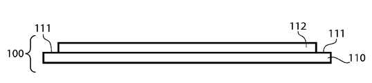
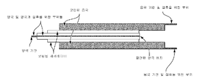
도 1a 내지 도 1d는 실시예들의 세트에 따른, 전기 비전도성 재료 층을 배치하는 방법을 도시하는 예시적인 단면 개략도들을 포함한다. 도 1a에서, 다층 구조물(100)은 서로 인접하게 배치되는 기판(110) 및 전극(112)을 포함한다. 몇몇의 실시예들에서, 전극(112)은 기판(110)의 위에 형성될 수 있다. 예를 들면, 전극(112)은 기판(110)의 위에 (예를 들면, 금속, 금속들의 혼합물, 또는 다른 적당한 재료의 진공 부착을 통해) 부착될 수 있다. 다른 예로서, 전극(112)은 캐스팅 공정에 의해 (예를 들면, 기판의 위에 전극 활성 재료를 포함하는 슬러리를 부착시키고 건조시킴으로써) 기판(110)의 위에 형성될 수 있다. 다른 실시예들에서, 전극(112)과 기판(110)은 별도의 독립체들로 형성될 수 있으며, 도 1a에 도시된 구조물을 형성하기 위해 함께 부착되거나 그렇지 않으면 접합될 수 있다. 여전히 다른 실시예들에서, 기판(110)과 전극(112)은 미리 조립된 다층의 구조물로서 제공될 수 있다.1A-1D include exemplary cross-sectional schematics illustrating a method of placing an electrically nonconductive material layer, in accordance with a set of embodiments. In FIG. 1A, the
몇몇의 실시예들에서, 도 1a에 도시된 실시예들의 세트와 같이, 전극(112)은 기판(110)을 완전히 커버하지는 않으며, 오히려 기판(110)의 에지 부분들(111)은 노출된 상태로 남겨진다. 이와 같은 배치는, 예를 들면, 기판이 조립된 전기화학 전지에서 집전장치를 지지하거나 집전장치로서 사용될 때 전기적 접촉들을 형성하는데 유용할 수 있다. 그러나, 다른 실시예들에서, 전극(112)은 기판(110)을 대체로 완전히 커버하도록 배치될 수 있다는 것이 이해되어야 한다.In some embodiments, like the set of embodiments shown in FIG. 1A, the
도 1b에서, 다층 구조물(100)은 전극(112)이 전기 비전도성 재료 층(114)과 기판(110) 사이에 있도록 전극(112)에 인접하게 배치되는 전기 비전도성 재료 층(114)을 더 포함한다. 아래에서 보다 상세하게 설명되는 바와 같이, 전기 비전도성 재료 층(114)은, 몇몇의 경우에, 다층 구조물(100)로부터 형성되는 전기화학 전지의 전해질의 전체 또는 일부분을 형성할 수 있다. 몇몇의 실시예들에서, 전기 비전도성 재료 층(114)은 전극(112)에 부착된다. 몇몇의 예에서, 전기 비전도성 재료 층(114)의 적어도 일부분은 전극(112)에 공유 결합된다.In FIG. 1B, the
몇몇의 실시예들에서, 전기 비전도성 재료 층(114)은 전극(112)의 위에 형성될 수 있다. 예를 들면, 전기 비전도성 재료 층(114)은 전극(112)의 위에 적용될 수 있으며, 예를 들면, (예를 들면, 전극의 위에 전기 비전도성 재료를 포함하는 슬러리를 부착시키고 건조시킴으로써) 캐스팅 공정을 사용하여 일정한 위치에 형성될 수 있다. 이와 같은 부착을 실행하기 위한 예시적인 방법들이, 예를 들면, 칼슨(Carlson) 등의 PCT 공개 번호 WO 99/33125와 배글리(Bagley) 등의 미국 특허 번호 5,194,341에 설명되며, 이들의 각각은 모든 목적을 위해 그 전체가 참고로 포함된다. 몇몇의 실시예들에서, 전기 비전도성 재료 층은, 예를 들면, 전자 빔 증발, 진공 열 증발, 레이저 어블레이션(ablation), 화학 증착, 열 증발, 플라스마 보조 화학 진공 부착, 레이저 증강 화학 증착, 제트 증착, 및 압출에 의해 부착될 수 있다. 전기 비전도성 재료 층은 또한 스핀 코팅 기술과 같은 방법들에 의해 부착될 수 있다. 예를 들면, 가교결합된 폴리머 층들을 부착시키기 위한 방법은, 예를 들면, 얄리지스(Yializis)의 미국 특허 번호 4,954,371에 설명된 바와 같은 플래시 증발 방법을 포함한다. 예를 들면, 리튬 염들을 포함하는 가교결합된 폴리머 층들을 부착시키기 위한 방법은, 예를 들면, 아핀토(Affinito) 등의 미국 특허 번호 5,681,615에 설명된 바와 같은 플래시 증발 방법을 포함할 수 있다. 전기 비전도성 재료 층을 부착시키는데 사용되는 기술은 부착되는 재료의 타입, 층의 두께 등에 의존할 수 있다. 전극의 위에 전기 비전도성 재료 층을 부착시키는 것은, 몇몇의 실시예들에서, 이것이 전기 비전도성 재료의 상대적으로 얇은 층들의 부착을 허용할 수 있기 때문에 유리할 수 있으며, 이는 최종의 전기화학 전지의 크기와 중량을 감소시킬 수 있다.In some embodiments, an electrically
다른 실시예들에서, 전기 비전도성 재료 층(114), 기판(110), 및 전극(112)은 별도의 독립체들로 형성될 수 있으며, 다층 구조물의 나머지에 부착되거나 그렇지 않으면 접합될 수 있다. 여전히 다른 실시예들에서, 기판(110), 전극(112), 및 전기 비전도성 재료 층(114)은 미리 조립된 다층 구조물로서 제공될 수 있다.In other embodiments, the electrically
기판(110), 전극(112) 및/또는 전기 비전도성 재료 층(114)(또는 다층 구조물의 다른 층들)은 몇몇의 실시예들에서 대체로 연속적인 층일 수 있다. 구조물의 두 개의 부분들 또는 층들 사이의 관계를 설명하는데 사용되는 바와 같은 "대체로 연속적인"은 이 부분들 또는 층들의 사이에 있는 구조물의 임의의 영역이 이 부분들 또는 층들과 본질적으로 동일하다는 것을 의미한다. 예를 들면, 그 자체에 대해 접히거나 다른 재료의 주변에 접힌, 재료의 대체로 연속적인 시트는 대체로 연속적인 시트의 일부로서 남아 있는 둘 이상의 부분들을 한정할 수 있다.
몇몇의 실시예들에서, 기판(110), 전극(112), 전기 비전도성 재료 층(114), 및/또는 여기에서 설명되는 다른 재료 층들에는 육안으로 보이는 불연속이 대체로 없을 수 있다. "육안으로 보이는 불연속이 대체로 없는" 층은 층의 나머지의 조성물과는 다른 재료(또는 재료들의 혼합물)로 만들어진, 층의 두께보다 더 두꺼운 층과 대체로 평행하게 측정되는, 최대 단면 치수를 가지는 영역을 포함하지 않는 층이다. 구체적인 예들로서, 공극을 대체로 가지지 않는 층에는 육안으로 보이는 불연속이 대체로 없을 수 있다. 게다가, 만약 층 내에 있는 구멍의 최대 단면 치수가 층의 두께보다 작다면 다공성 재료 층에는 육안으로 보이는 불연속이 대체로 없을 수 있다. 그러나, 다공성 재료의 층의 두께보다 큰 구멍 크기를 가지는 다공성 재료에는 육안으로 보이는 불연속이 대체로 있을 수 있을 것이다. 게다가, 벌크 재료 및 벌크 재료 내의 재료의 두께보다 큰 최대 단면 치수를 가지는 제2 재료의 섬을 포함하는 재료에는 육안으로 보이는 불연속이 대체로 있을 수 있을 것이다.In some embodiments, the
도 1b에 도시된 바와 같이, 전기 비전도성 재료 층(114)은 전극(112)과 기판(110)을 대면하지 않는 제1의 대체로 평평한 표면(120), 및 전극(112)과 기판(110)을 대면하는 (경계면(122)에 있는) 제2의 대체로 평평한 표면을 포함한다. 게다가, 전극(112)은 전기 비전도성 재료 층(114)을 대면하고 기판(110)을 대면하지 않는 (경계면(122)에 있는) 제1의 대체로 평평한 표면뿐만 아니라 기판(110)을 대면하고 전기 비전도성 재료 층(114)을 대면하지 않는 (경계면(124)에 있는) 제2의 대체로 평평한 표면을 포함한다. 기판(110)은 전극(112)과 전기 비전도성 재료 층(114)을 대면하는 (경계면(124)에 있는) 제1의 대체로 평평한 표면 및 전극(112)과 전기 비전도성 재료 층(114)을 대면하지 않는 제2의 대체로 평평한 표면(126)을 포함한다.As shown in FIG. 1B, the electrically
여기에서 사용되는 바와 같이, 표면(또는 표면 부분)은 표면과 물체가 대체로 평행할 때 물체에 "대면하는" 것으로 언급되며, 표면을 포함하는 재료의 벌크에 대해 수직이고 이로부터 멀어지게 연장되는 라인은 물체와 교차한다. 예를 들면, 만약 제1 표면에 대해 수직이고 제1 표면을 포함하는 재료의 벌크로부터 멀어지게 연장되는 라인이 제2 표면과 교차한다면, 제1 표면(또는 제1 표면 부분)과 제2 표면(또는 제2 표면 부분)은 서로를 대면할 수 있다. 만약 표면에 대해 수직이고 표면을 포함하는 재료의 벌크로부터 멀어지게 연장되는 라인이 층과 교차한다면, 표면과 층은 서로를 대면할 수 있다. 표면은 이것이 다른 물체와 접촉할 때, 또는 하나 이상의 중간 재료들이 표면과 다른 물체 사이에 배치될 때 다른 물체를 대면할 수 있다. 예를 들면, 서로를 대면하는 두 개의 표면들은 접촉할 수 있거나 이들 사이에 하나 이상의 중간 재료들을 포함할 수 있다.As used herein, a surface (or surface portion) is referred to as "facing" an object when the surface and the object are generally parallel, a line perpendicular to and extending away from the bulk of the material comprising the surface. Intersects the object. For example, if a line perpendicular to the first surface and extending away from the bulk of material comprising the first surface intersects the second surface, the first surface (or first surface portion) and the second surface ( Or second surface portions) may face each other. If a line perpendicular to the surface and extending away from the bulk of the material comprising the surface intersects the layer, the surface and layer may face each other. The surface may face another object when it contacts another object or when one or more intermediate materials are placed between the surface and the other object. For example, two surfaces facing each other may contact or include one or more intermediate materials therebetween.
여기에서 사용되는 바와 같이, 표면(또는 표면 부분)은 표면과 물체가 대체로 평행할 때 물체를 "대면하는" 것으로 언급되며, 표면을 포함하는 재료의 벌크에 수직이고 이로부터 멀어지게 연장되는 라인은 물체와 교차하지 않는다. 예를 들면, 만약 제1 표면에 수직이고 제1 표면을 포함하는 재료의 벌크로부터 멀어지게 연장되는 라인이 제2 표면과 교차하지 않는다면, 제1 표면(또는 제1 표면 부분)과 제2 표면(또는 제2 표면 부분)은 서로 대면하지 않을 수 있다. 만약 표면에 수직이고 표면을 포함하는 재료의 벌크로부터 멀어지게 연장되는 라인이 층과 교차한다면, 표면과 층은 서로 대면하지 않을 수 있다. 몇몇의 실시예들에서, 만약 표면과 물체에 의해 한정되는 최대 각도가 약 10°보다 작거나, 약 5° 보다 작거나, 약 2° 보다 작거나, 또는 약 1°보다 작다면, 표면과 다른 물체(예를 들면, 다른 표면, 층 등)는 대체로 평행할 수 있다.As used herein, a surface (or surface portion) is referred to as "facing" an object when the surface and the object are generally parallel, and a line perpendicular to and extending away from the bulk of the material comprising the surface Do not intersect the object. For example, if the line perpendicular to the first surface and extending away from the bulk of the material comprising the first surface does not intersect the second surface, the first surface (or first surface portion) and the second surface ( Or the second surface portion) may not face each other. If the line perpendicular to the surface and extending away from the bulk of the material comprising the surface intersects the layer, the surface and the layer may not face each other. In some embodiments, if the maximum angle defined by the surface and the object is less than about 10 °, less than about 5 °, less than about 2 °, or less than about 1 °, Objects (eg, other surfaces, layers, etc.) may be generally parallel.
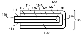
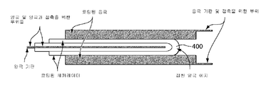
다층 구조물은 접힌 구조물을 형성하기 위해 축을 따라 접힐 수 있다. 몇몇의 실시예들에서, 다층 구조물은 전극의 표면의 제1 부분과 제2 부분(예를 들면, 전기 비전도성 재료 층을 대면하지 않는 표면의 제1 부분과 제2 부분)이 서로 대면하도록 접힐 수 있다. 예를 들면, 도 1b 및 도 1c에 도시된 실시예들의 세트에서, 도 1b의 다층 구조물(100)은 도 1c의 다층 구조물을 형성하기 위해 화살표(132)의 방향으로 (페이지를 통과해 연장되는) 축(130)을 따라 접힌다. 원래는 도 1b의 전기 비전도성 재료 층(114)을 대면하지 않는 전극(112)의 표면 부분들(및 124B) 모두는 이들이 서로를 대면하도록 도 1c의 구조물로 재배향되었다. 도 1c에 도시된 바와 같이, 표면 부분들(124A 및 124B)은 이들 사이에 중간 재료(기판(110))를 포함한다. 그러나, 다른 실시예들에서, 표면 부분들(124A 및 124B)은 접촉 상태에 있을 수 있다.The multilayer structure may be folded along an axis to form a folded structure. In some embodiments, the multilayer structure is folded such that the first portion and the second portion of the surface of the electrode (eg, the first portion and the second portion of the surface not facing the layer of non-conductive material) face each other. Can be. For example, in the set of embodiments shown in FIGS. 1B and 1C, the
다층 구조물을 이런 방식으로 접음으로써, 전기 비전도성 재료 층의 부분(136)은 전극(112)의 접힌 에지의 볼록한 표면 부분의 위에 배향되도록 배치된다. 몇몇의 경우에, 전기 비전도성 재료 층은 전극(112)의 에지를 대체로 커버할 수 있다. 전극(112)의 접힌 에지의 위에 전기 비전도성 재료의 (부분(136)과 같은) 부분을 가지는 것은 전극(112)과 전기 비전도성 재료 층(114)의 위에 배치되는 연이어지는 전극들 사이의 단락을 방지하는데 유용할 수 있다.By folding the multilayer structure in this manner, the
추가적인 전극들이 또한 다층 구조물에 포함될 수 있다. 도 1d에 도시된 실시예들의 세트에서, 전극들(140 및 142)은 전기 비전도성 재료 층(114)에 인접하게 배치된다. 이런 방식으로 배치될 때, 전기 비전도성 재료 층은 전극들(112 및 140) 사이에 있는 제1 부분(146) 및 전극들(112 및 142)사이에 있는 제2 부분(148)을 포함한다. 게다가, 제1 및 제2 부분들(146 및 148)은 각각, 부분(136)에 의해 직접 연결된다. 두 개의 구성요소들 또는 하나의 구성요소의 부분들은 대체로 상이한 조성물을 가지는 영역을 통과하지 않고 두 개의 부분들 또는 구성요소들을 연결하는 라인이 그려질 수 있을 때 "직접 연결되는" 것으로 또는 "직접 접촉하는" 것으로 언급된다. 도 1d에 도시된 실시예들의 세트에서, 제1 및 제2 부분들(146 및 148)은 비록 이들이 모든 실시예들에 있을 필요는 없지만 또한 대체로 연속적이다.Additional electrodes may also be included in the multilayer structure. In the set of embodiments shown in FIG. 1D, the
전극들(140 및 142) 중의 하나 또는 둘 모두는 전기 비전도성 재료 층(114)의 위에 형성될 수 있다. 예를 들면, 전극(140 및/또는 142)은 재료 층(114)의 위에 (예를 들면, 진공 부착을 통해) 부착될 수 있거나 (예를 들면, 건조된 슬러리로서) 캐스팅될 수 있다. 다른 실시예들에서, 전극(140 및/또는 142)은 별도의 독립체들로서 형성될 수 있으며, 다층 구조물에 부착되거나 그렇지 않으면 접합될 수 있다. 두 개의 추가적인 전극들(140 및 142)이 도 1d에 도시되지만, 다른 실시예들에서, 단지 하나의 추가적인 전극(예를 들면, 전극(140)만)이 다층 구조물에 포함될 수 있다는 것이 이해되어야 한다.One or both of the
몇몇의 실시예들에서, 은전기비전도성재료층(114)에 부착된다. 몇몇의 예에서, 전극(140) 및/또는 전극(142)의 적어도 일부분은 전기 비전도성 재료 층(114)에 공유 결합된다.In some embodiments, a silver
전극들의 극성은 전기화학 전지를 제조하기 위해 선택될 수 있다. 몇몇의 실시예들에서, 전극(112)은 제1 극성을 가질 수 있지만, 전극(140)(및 만약 존재한다면, 142)은 반대인 제2 극성을 가질 수 있다. 일반적으로, 두 개의 전극들은 만약 하나가 양극이고 다른 하나가 음극이라면 반대의 극성을 가진다. 예를 들면, 전극(112)은 양극일 수 있지만 전극(140)(및 만약 존재한다면, 142)은 음극일 수 있다. 다른 경우에, 전극(112)은 음극일 수 있지만 전극(140)(및 만약 존재한다면, 142)은 양극일 수 있다.The polarity of the electrodes can be selected to produce an electrochemical cell. In some embodiments,
임의의 적당한 기술을 사용하여 전극들에 대한 전기적 접촉이 만들어질 수 있다. 도 1d에 도시된 실시예들의 세트에서, 전기 전도성 기판(110)을 사용함으로써 전극(112)에 대한 전기적 접촉이 만들어질 수 있다. 기판(110)은 전기 전도성 벌크 재료 또는 전기 전도성 재료로 코팅되는 전기 비전도성 벌크 재료를 포함할 수 있다. 집전장치들(144A 및 144B)을 각각 다층 구조물에 포함시킴으로써 전극들(140 및/또는 142)에 대한 전기적 접촉이 만들어질 수 있다.Electrical contact can be made to the electrodes using any suitable technique. In the set of embodiments shown in FIG. 1D, electrical contact to electrode 112 can be made by using an electrically
부분(예를 들면, 층, 구조물, 영역)이 다른 부분의 "위에(on)" 있거나, 이에 "인접하고" 있거나, 이의 "상부에(above)" 있거나, 이의 "위에(over)"있거나, 이를 "덮고"있거나, 이에 "의해 지지되고" 있을때에, 이는 직접 다른 부분의 위에 있을 수 있거나, 중간 부분(예를 들면, 층, 구조물, 영역)이 또한 존재할 수 있다고 이해되어야 한다. 유사하게, 부분이 다른 부분의 "아래에" 있거나, 이의 "하부에" 있을 때, 이는 직접 다른 부분의 아래에 있을 수 있거나, 중간 부분(예를 들면, 층, 구조물, 영역)이 또한 존재할 수 있다. 다른 부분의 "직접 위에" 있거나, 이에 "바로 인접하고" 있거나, 이와 "접촉하고"있거나, 이에 "의해 직접 지지되는" 부분은 중간 부분이 존재하지 않는다는 것을 의미한다. 부분이 다른 부분의 "위에(on)" 있거나, 이의 "상부에" 있거나, 이에 "인접하고" 있거나, 이의 "위에(over)" 있거나, 이를 "덮고" 있거나, 이와 "접촉하고" 있거나, 이의 "아래에" 이에 "의해 지지되는것으로 언급될 때, 이는 다른 부분의 전체 또는 일부분을 커버할 수 있다는 것이 또한 이해되어야 한다.A portion (eg, layer, structure, region) is “on”, “adjacent” to it, “above” thereof, “over” thereof, or When it is "covering" or "supported" by it, it should be understood that it may be directly on top of another part, or an intermediate part (eg a layer, structure, area) may also be present. Similarly, when a part is "below" or "below" of another part, it may be directly below another part, or an intermediate part (eg, layer, structure, area) may also be present. have. A portion that is "directly on", "immediately adjacent" to, "in contact with", or "directly supported by" another portion means that there is no intermediate portion. A portion is "on" another, "on top" of it, "adjacent" to it, "over" it, "covers" it, "contacts" it, or When referred to as "supported by" below, it should also be understood that this may cover all or part of another portion.
그러므로, 도 1a 내지 도 1d에 도시된 실시예들에서, 그리고 여기에서 설명된 다른 실시예들에서, 하나 이상의 추가적인 층들이 도면들에 도시된 층들 사이에 배치될 수 있다는 것이 이해되어야 한다. 예를 들면, 아래에서 설명되는 바와 같이 다층 구조물(100)을 접기 전에 기판을 제거하는데 사용될 수 있는 분리 층과 같은 하나 이상의 추가적인 층들이 기판(110)과 전극(112) 사이에 배치될 수 있다는 것이 이해되어야 한다. 게다가, 하나 이상의 추가적인 층들이 분리 층과 기판 사이에 배치될 수 있다. 게다가, 하나 이상의 층들이 다층 구조물의 다른 구성요소들의 사이에 배치될 수 있다. 예를 들면, 하나 이상의 프라이머 층들이 층들 사이의 부착을 용이하게 하기 위해 집전장치와 전극 층 사이에 배치될 수 있다. 적당한 프라이머 층들의 예는 그 전체가 참고로 여기에 포함되고, 2008년 10월 23일에 출원되었으며 "배터리 전극을 위한 프라이머(Primer For Battery Electrode)" 를 명칭으로 하는 국제 공개 번호 WO 2009/054987로 공개된 국제 특허 출원 번호 PCT/US2008/012042에서 설명된다. 게다가, 하나 이상의 층들은 전극과 전기 비전도성 재료 층 사이에 배치될 수 있다. 예를 들면, 하나 이상의 층들은 전극(112)과 전기 비전도성 재료 층(114) 사이에, 전극(140)과 전기 비전도성 재료 층(114) 사이에, 및/또는 전극(142)과 전기 비전도성 재료 층(114) 사이에 배치될 수 있다. 물론, 다른 실시예들에서, 기판(110)과 전극(112)이 접촉될 수 있으며, 전극(112)과 전기 비전도성 재료 층(114)이 접촉될 수 있으며, 전기 비전도성 재료 층(114)과 전극(140)이 접촉될 수 있으며/있거나, 전기 비전도성 재료 층(114)과 전극(142)이 접촉될 수 있다. 게다가, 몇몇의 경우에, 전극(140 및/또는 142)은 집전장치(144A 및 144B)와 각각 접촉될 수 있지만, 다른 경우에, 하나 이상의 재료들이 전극(140)과 이의 집전장치 사이 및/또는 전극(142)와 이의 집전장치 사이에 배치될 수 있다.Therefore, in the embodiments shown in FIGS. 1A-1D, and in the other embodiments described herein, it should be understood that one or more additional layers may be disposed between the layers shown in the figures. For example, one or more additional layers may be disposed between the
본 발명의 몇몇의 실시예들은 여기에서 설명되는 구성요소들(또는 이들의 부분들)의 상대적인 위치와 관련된다. 몇몇의 실시예들에서, 다층 구조물(또는 다층 구조물을 포함하는 전기화학 전지)은, 선택적으로 설명된 층들 사이에 개재되는 동일하거나 상이한 재료의 임의의 수의 다른 층들과 함께, (예를 들면, 도 1d의 화살표(160)를 따라 발견되는) 설명된 순서로 배치되는 다음의 층들을 포함할 수 있다: 제1 극성을 가지는 제1 전극 층 부분(예를 들면, 도 1d의 전극(140)의 부분), 제2 극성을 가지는 제2 전극 층 부분(예를 들면, 도 1d의 기판(110)의 위에 있는 전극(112)의 부분), 제2 극성을 가지는 제3 전극 층 부분(예를 들면, 도 1d의 기판(110)의 아래에 있는 전극(112)의 부분), 및 제1 극성을 가지는 제4 전극 층 부분(예를 들면, 도 1d의 전극(142)의 부분). 몇몇의 경우에, 도 1d에 도시된 실시예들에서와 같이, 제2 및 제3 전극 층 부분들은 단일의, 대체로 연속적인 전극의 부분들이다. 게다가, 몇몇의 경우에, 제1 극성을 가지는 전극 부분들은 제2 전극 층 부분과 제3 전극 층 부분 사이에 개재되어 배치되지 않는다. 도 1d에서, 예를 들면, (전극이 아닌) 기판(110)만이 제2 전극 층 부분(예를 들면, 도 1d의 기판(110)의 위에 있는 전극(112)의 부분)과 제3 전극 층 부분(예를 들면, 도 1d의 기판(110)의 아래에 있는 전극(112)의 부분) 사이에 배치된다.Some embodiments of the invention relate to the relative position of the components (or portions thereof) described herein. In some embodiments, a multilayer structure (or electrochemical cell comprising a multilayer structure) is optionally (eg, with any number of other layers of the same or different material interposed between the described layers). The following layers may be arranged in the described order (found along
몇몇의 실시예들에서, 다층 구조물(또는 다층 구조물을 포함하는 전기화학 전지)은 제1 기판 표면 부분(예를 들면, 전극(112)의 표면 부분(124A)에 인접한 기판 표면 부분)과 제1 기판 표면 부분을 대면하지 않는 제2 기판 표면 부분(예를 들면, 전극(112)의 표면 부분(124B)에 인접한 기판 표면 부분)을 가지는 기판을 포함할 수 있다. 다층 구조물은 또한 제1 기판 표면 부분에 인접한 제1 부분(예를 들면, 도 1d의 기판의 위에 있는 전극(112)의 부분)과 제2 기판 표면 부분에 인접한 제2 부분(예를 들면, 도 1d의 기판의 아래에 있는 전극(112)의 부분)을 가지는 제1 전극을 포함할 수 있다. 게다가, 다층 구조물은 제1 전극의 제1 부분을 대면하는 제1 표면 부분(예를 들면, 경계면(150A)에 있는 전극(140)의 표면)과 제2 전극의 제1 표면 부분을 대면하지 않는 제2 표면 부분(예를 들면, 상부 집전장치(144A)를 대면하는 전극(140)의 표면)을 가지는 제2 전극(예를 들면, 전극(140)에 추가하거나 이를 대신하여, 전극(142)이 또한 포함될 수 있지만, 도 1d의 전극(140))을 포함할 수 있다. 게다가, 다층 구조물은 제1 전극의 제1 부분과 제2 전극의 제1 표면 부분 사이에 있는 제1 부분(예를 들면, 전기 비전도성 재료 층(114)의 부분(146)), 제1 전극의 제2 표면 부분에 인접한 제2 부분(예를 들면, 전기 비전도성 재료 층(114)의 부분(148)), 및 제1 부분과 제2 부분에 직접 접촉하는 제3 부분(예를 들면, 전기 비전도성 재료 층(114)의 부분(136))을 가지는 대체로 연속적인, 전기 비전도성 재료 층(예를 들면, 도 1d의 층(114))을 포함할 수 있다.In some embodiments, the multilayer structure (or electrochemical cell comprising the multilayer structure) may comprise a first substrate surface portion (eg, a substrate surface portion adjacent to the
전기 비전도성 재료 층은 임의의 적당한 두께를 가질 수 있다. 몇몇의 실시예들에서, 상대적으로 얇은 전기 비전도성 재료 층이 사용될 수 있으며, 이는 다층 구조물의 체적 및/또는 중량을 감소시킬 수 있으며, 그에 의해 다층 구조물을 사용하여 제조된 전기화학 전지의 비에너지와 에너지 밀도를 증가시킬 수 있다. 몇몇의 실시예들에서, 전기 비전도성 재료 층은 약 100 미크론보다 작거나; 약 50 미크론보다 작거나; 약 20 미크론보다 작거나; 약 10 미크론보다 작거나; 약 5 미크론보다 작거나; 약 1 미크론보다 작거나; 적어도 약 0.1 미크론이고 약 100, 50, 20, 10, 5, 또는 1 미크론보다 작거나; 적어도 약 0.5 미크론이고 약 100, 50, 20, 10, 5, 또는 1 미크론보다 작거나; 적어도 약 1 미크론이고 약 100, 50, 20, 10, 또는 5 미크론보다 작은 평균 두께를 가질 수 있다. 몇몇의 경우에, (예를 들면, 도 1c 및 도 1d의 경계면(122)에 있는) 전극(112)의 최외측 표면과 (예를 들면, 각각 도 1d의 경계면(150A 및 150B)에 있는) 전극(140) 및/또는 전극(142)의 최내측 표면 사이의 평균 거리는 약 100 미크론보다 작거나; 약 50 미크론보다 작거나; 약 20 미크론보다 작거나; 약 10 미크론보다 작거나; 약 5 미크론보다 작거나; 약 1 미크론보다 작거나; 적어도 약 0.1 미크론이고 약 100, 50, 20, 10, 5, 또는 1 미크론보다 작거나; 적어도 약 0.5 미크론이고 약 100, 50, 20, 10, 5 또는 1 미크론보다 작거나; 적어도 약 1 미크론이고 약 100, 50, 20, 10, 또는 5 미크론보다 작을 수 있다.The electrically nonconductive material layer can have any suitable thickness. In some embodiments, a relatively thin layer of electrically nonconductive material can be used, which can reduce the volume and / or weight of the multilayer structure, thereby reducing the specific energy of an electrochemical cell produced using the multilayer structure. And increase the energy density. In some embodiments, the electrically nonconductive material layer is less than about 100 microns; Less than about 50 microns; Less than about 20 microns; Less than about 10 microns; Less than about 5 microns; Less than about 1 micron; At least about 0.1 micron and less than about 100, 50, 20, 10, 5, or 1 micron; At least about 0.5 micron and less than about 100, 50, 20, 10, 5, or 1 micron; And have an average thickness of at least about 1 micron and less than about 100, 50, 20, 10, or 5 microns. In some cases, the outermost surface of electrode 112 (eg, at
몇몇의 실시예들에서, 전극과 전기 비전도성 재료 층은 전압이 전극들에 그리고 건조된 전기 비전도성 재료 층에 걸쳐(즉, 액체 전해질과 같은 임의의 유체의 추가 전에) 가해질 때, 상대적으로 높은 전기 저항이 유지되도록 구성되고 배치될 수 있다. 몇몇의 경우에, 건조된 다층 구조물 내에 있는 양극과 음극 사이의 전기 저항은 적어도 약 1 볼트의 전압이 양극과 음극에 걸쳐 가해질 때 적어도 약 100 옴이거나, 적어도 약 1000 옴이거나, 적어도 약 10 킬로옴이거나, 적어도 약 100 킬로옴이거나, 적어도 약 1 메가옴이거나, 적어도 약 10 메가옴이다. 다층 구조물 내에서 양극과 음극 사이에 있는 재료에 걸쳐 전압 강하를 적용하고 멀티미터를 사용하여 그 결과로 나온 저항을 측정함으로써 본 기술분야의 통상의 기술자는 이와 같은 측정을 할 수 있을 것이다. 몇몇의 실시예들에서, 위에서 약술된 전기 저항은 (여기에서 설명된 임의의 압력을 한정하는 이방성 힘을 포함하는) 이방성 힘을 가하는 동안 유지될 수 있다.In some embodiments, the electrode and the electrically nonconductive material layer are relatively high when a voltage is applied to the electrodes and across the dried electrically nonconductive material layer (ie, prior to the addition of any fluid, such as a liquid electrolyte). It can be constructed and arranged so that the electrical resistance is maintained. In some cases, the electrical resistance between the anode and the cathode in the dried multilayer structure is at least about 100 ohms, at least about 1000 ohms, or at least about 10 kiloohms when a voltage of at least about 1 volt is applied across the anode and the cathode. Or at least about 100 kiloohms, at least about 1 megohm, or at least about 10 megohms. One of ordinary skill in the art would be able to make this measurement by applying a voltage drop across the material between the anode and cathode in a multilayer structure and measuring the resulting resistance using a multimeter. In some embodiments, the electrical resistance outlined above may be maintained while applying an anisotropic force (including an anisotropic force that defines any pressure described herein).
몇몇 경우에, 건조된 전기 비전도성 재료 층의 두께를 통한 (즉, 액체 전해질과 같은 임의의 유체의 부착 전의) 전기 저항은, 적어도 약 1 볼트의 전압이 양극과 음극에 걸쳐 가해질 때, 적어도 약 100 옴이거나, 적어도 약 1000 옴이거나, 적어도 약 10 킬로옴이거나, 적어도 약 100 킬로옴이거나, 적어도 약 1 메가옴이거나, 또는 적어도 약 10 메가옴이다. 본 기술분야의 통상의 기술자는 (예를 들면, 서로 대면하지 않는 전기 비전도성 재료 층의 표면들에 전극들을 부착함으로써) 전기 비전도성 재료 층의 두께를 통한 전압 강하를 적용하고 멀티미터를 사용하여 그 결과로 나온 저항을 측정함으로써 이와 같은 측정을 할 수 있을 것이다. 몇몇의 실시예들에서, 위에서 약술된 전기 저항은 (여기에서 설명된 임의의 압력을 한정하는 이방성 힘을 포함하는) 이방성 힘을 가하는 동안 유지될 수 있다.In some cases, the electrical resistance through the thickness of the layer of dried non-conductive material (ie, prior to the attachment of any fluid, such as a liquid electrolyte) is at least about when a voltage of at least about 1 volt is applied across the anode and cathode. 100 ohms, at least about 1000 ohms, at least about 10 kiloohms, at least about 100 kiloohms, at least about 1 megaohms, or at least about 10 megaohms. One skilled in the art applies a voltage drop through the thickness of the electrically nonconductive material layer (eg, by attaching electrodes to the surfaces of the non-conductive material layer that are not facing each other) and uses a multimeter. You can do this by measuring the resulting resistance. In some embodiments, the electrical resistance outlined above may be maintained while applying an anisotropic force (including an anisotropic force that defines any pressure described herein).
전기 비전도성 재료 층은 (예를 들면, 사용 중에, 예컨대 전기화학 전지의 충전 및/또는 방전 중에) 단락을 방지하기 위해 양극과 음극을 서로로부터 분리하거나 절연시킬 수 있는 임의의 재료를 포함할 수 있지만, 양극과 음극 사이에 이온의 이동을 허용하도록 구성되고 배치될 수 있다. 몇몇의 실시예들에서, 전기 비전도성 재료 층의 전체 또는 일부분은 적어도 약 104,적어도 약 105,적어도 약 1010,적어도 약 1015,또는 적어도 약 1020옴 미터의 벌크 저항률을 가지는 재료로 형성될 수 있다.The electrically nonconductive material layer may comprise any material that can separate or insulate the positive and negative electrodes from each other to prevent a short circuit (eg, during use, such as during charging and / or discharging of an electrochemical cell). However, it can be constructed and arranged to allow the movement of ions between the anode and the cathode. In some embodiments, all or a portion of the layer of electrically nonconductive material has a bulk resistivity of at least about 10 4 , at least about 10 5 , at least about 10 10 , at least about 10 15 , or at least about 10 20 ohm meters. It can be formed as.
몇몇의 실시예들에서, 전기 비전도성 재료 층은 다층 구조물로부터 형성되는 전기화학 전지의 전해질일 수 있다. 다른 경우들에서, 전기 비전도성 재료 층은 다층 구조물로부터 형성되는 전기화학 전지의 전해질로부터 분리된 층일 수 있다 (즉, 전기화학 전지는 전기 비전도성 재료 층으로부터 분리된 전해질 층을 포함할 수 있다).In some embodiments, the electrically nonconductive material layer can be an electrolyte of an electrochemical cell formed from a multilayer structure. In other cases, the electrically nonconductive material layer may be a layer separate from the electrolyte of the electrochemical cell formed from the multilayer structure (ie, the electrochemical cell may comprise an electrolyte layer separated from the electroconductive material layer). .
전기 비전도성 재료 층의 전체 또는 일부분은, 몇몇의 실시예들에서, 고체 전해질로 형성될 수 있다. 음극으로부터 양극을 전기 절연하는 것에 추가하여, 고체 전해질은 이온 전도성일 수 있으며, 그에 의해 양극과 음극 사이에 이온의 이동을 허용할 수 있다. 유용한 고체 폴리머 전해질들의 예는 폴리에테르들, 폴리에틸렌 옥사이드들, 폴리프로필렌 옥사이드들, 폴리이미드들, 폴리포스파젠들, 폴리아크릴로니트릴들, 폴리실록산들, 위에서 언급된 것들의 유도체들, 위에서 언급된 것들의 코폴리머들, 위에서 언급된 것들의 가교결합된 망상 구조물들, 및 위에서 언급된 것들의 혼합물들로 이루어지는 그룹으로부터 선택되는 하나 이상의 폴리머들을 포함하는 것들을 포함하지만, 이들에 한정되지 않는다.All or part of the layer of electrically nonconductive material may, in some embodiments, be formed of a solid electrolyte. In addition to electrically insulating the positive electrode from the negative electrode, the solid electrolyte may be ion conductive, thereby allowing the movement of ions between the positive electrode and the negative electrode. Examples of useful solid polymer electrolytes are polyethers, polyethylene oxides, polypropylene oxides, polyimides, polyphosphazenes, polyacrylonitriles, polysiloxanes, derivatives of those mentioned above, those mentioned above Copolymers, crosslinked network structures of those mentioned above, and those comprising one or more polymers selected from the group consisting of mixtures of those mentioned above.
몇몇의 실시예들에서, 전기 비전도성 재료 층의 전체 또는 일부분은 겔로 형성될 수 있다. 여기에서 사용되는 바와 같이, 용어 "겔"은 액체와 바인더 성분을 포함하는 삼차원 망을 가리키며, 여기서 액체는 바인더에 의해 흡수되며, 바인더를 통해 유동되도록 허용되지 않는다. 액체를 고체 망에 가하는 중에 액체가 삼차원 망의 고체들 내에서 흡수될 때, 겔이 형성될 수 있다. 몇몇의 경우에, 겔 내에 있는 삼차원 망은 폴리머(예를 들면, 가교결합된 폴리머) 내에 흡수되는 액체를 포함할 수 있다. 본 기술분야의 통상의 기술자는, 예를 들면, 디부틸 프탈레이트(DBP) 흡수 시험을 통해 겔의 흡수 강성을 측정함으로써 겔과 고체 및 유체의 다른 조합들(예를 들면, 다공성 세퍼레이터와 액체 용매) 사이의 차이를 판단할 수 있을 것이다. 일반적으로, 액체에 대한 겔의 바인더 성분의 노출 중에, 겔의 중량은 증가될 것이지만, 다공성 세퍼레이터의 중량은 대체로 증가하지 않을 것이다. 몇몇의 실시예들에서, 겔의 바인더 성분은 약 10 미크론보다 크거나 약 1 미크론보다 큰 구멍들을 실질적으로 가지지 않고 액체를 흡수할 수 있다. 겔의 바인더 성분에는 몇몇의 경우에 구멍들이 대체로 없을 수 있다. 전기 비전도성 재료 층들에 사용하기 위한 유용한 겔 폴리머들의 예는 폴리에틸렌 옥사이드들, 폴리프로필렌 옥사이드들, 폴리아크릴로니트릴들, 폴리실록산들, 폴리이미드들, 폴리포스파젠들, 폴리에테르들, 설폰화 폴리이미드들, 퍼플루오르화 멤브레인들(NAFION 수지들), 폴리디비닐 폴리에틸렌 글리콜들, 폴리에틸렌 글리콜 디아크릴레이트들, 폴리에틸렌 글리콜 디메타크릴레이트들, 위에서 언급된 것들의 유도체들, 위에서 언급된 것들의 코폴리머들, 위에서 언급된 것들의 가교결합된 망상 구조들, 및 위에서 언급된 것들의 혼합물들로 이루어지는 그룹으로부터 선택되는 하나 이상의 폴리머들, 및 선택적으로, 하나 이상의 가소제들을 포함하는 것들을 포함하지만, 이들에 한정되지 않는다.In some embodiments, all or part of the layer of electrically nonconductive material may be formed of a gel. As used herein, the term "gel" refers to a three-dimensional network comprising a liquid and a binder component, where the liquid is absorbed by the binder and is not allowed to flow through the binder. When the liquid is absorbed in the solids of the three-dimensional network while adding the liquid to the solid network, a gel can be formed. In some cases, the three-dimensional network in the gel may comprise a liquid that is absorbed in a polymer (eg, a crosslinked polymer). Those skilled in the art will appreciate that gels, solids and other combinations of fluids (eg, porous separators and liquid solvents), for example, by measuring the absorption stiffness of the gel through a dibutyl phthalate (DBP) absorption test. You can judge the difference between them. In general, during exposure of the binder component of the gel to the liquid, the weight of the gel will increase, but the weight of the porous separator will generally not increase. In some embodiments, the binder component of the gel can absorb liquid without substantially having pores larger than about 10 microns or larger than about 1 micron. The binder component of the gel may in some cases be generally free of pores. Examples of useful gel polymers for use in electrically nonconductive material layers include polyethylene oxides, polypropylene oxides, polyacrylonitriles, polysiloxanes, polyimides, polyphosphazenes, polyethers, sulfonated polyimides , Perfluorinated membranes (NAFION resins), polydivinyl polyethylene glycols, polyethylene glycol diacrylates, polyethylene glycol dimethacrylates, derivatives of those mentioned above, copolymers of those mentioned above These include, but are not limited to, those comprising one or more polymers selected from the group consisting of crosslinked network structures of those mentioned above, and mixtures of those mentioned above, and optionally, one or more plasticizers. It doesn't work.
몇몇의 실시예들에서, 전기 비전도성 재료의 적어도 일부분은 액체 전해질로 부분적으로 또는 대체로 채워진 고체의, 전기 비전도성 재료로 형성될 수 있다. 몇몇의 이와 같은 실시예들에서, 액체 전해질로 부분적으로 또는 대체로 채워진 고체 재료는 전기화학 전지를 위한 전해질로서 역할을 할 수 있다. 고체의, 전기 비전도성 재료는, 몇몇의 실시예들에서, 대체로 이온 비전도성일 수 있다. 다른 경우들에서, 고체의, 전기 비전도성은 이온 전도성일 수 있으며, 액체 전해질이 (조합의 고체 부분의 전도성과 비교하여) 향상된 이온 전도성을 가지는 조합된 구조를 제조하는데 사용될 수 있다.In some embodiments, at least a portion of the electrically nonconductive material may be formed of a solid, electrically nonconductive material partially or generally filled with a liquid electrolyte. In some such embodiments, a solid material partially or generally filled with a liquid electrolyte may serve as an electrolyte for an electrochemical cell. The solid, electrically nonconductive material may, in some embodiments, be generally ion nonconductive. In other cases, the solid, electrical non-conductivity may be ion conductive and the liquid electrolyte may be used to produce a combined structure having improved ion conductivity (compared to the conductivity of the solid portion of the combination).
다양한 고체, 전기 비전도성 세퍼레이터 재료들이 본 기술분야에 알려져 있다. 적당한 고체 다공성 세퍼레이터 재료들의 예는, 예를 들면, 폴리에틸렌들 및 폴리프로필렌들과 같은 폴리올레핀들, 유리 섬유 필터 종이들, 및 세라믹 재료들을 포함하지만, 이들에 한정되지 않는다. 본 발명에 사용하기에 적합한 세퍼레이터들과 세퍼레이터 재료들의 다른 예는 공동 출원인인 칼슨 등의 미국 특허 출원 번호 08/995,089 및 09/215,112에 설명된 바와 같이, 프리 스탠딩 필름(free standing film)으로서 또는 전극들 중의 하나의 위의 직접 코팅 적용에 의해 제공될 수 있는 미세다공성 크세로겔 층, 예를 들면 미세다공성 유사 베마이트 층을 포함하는 것들이다. 고체 전해질들과 겔 전해질들은 또한 이들의 전해질 기능에 추가하여 세퍼레이터로서 기능을 할 수 있다.Various solid, electrically nonconductive separator materials are known in the art. Examples of suitable solid porous separator materials include, but are not limited to, for example, polyolefins such as polyethylenes and polypropylenes, glass fiber filter papers, and ceramic materials. Other examples of separators and separator materials suitable for use in the present invention are as free standing films or electrodes, as described in co-applicant US Pat. Appl. Nos. 08 / 995,089 and 09 / 215,112 to Carlson et al. Microporous xerogel layers, such as microporous pseudo boehmite layers, which can be provided by direct coating application on one of them. Solid electrolytes and gel electrolytes can also function as separators in addition to their electrolyte function.
위에서 언급된 바와 같이, 액체 전해질은 이온 전도성을 향상시키는데 사용될 수 있다. 몇몇의 실시예들에서, 액체 전해질은 이온 전도성을 증가시키기 위해 하나 이상의 이온성 전해질 염들을 포함할 수 있다. 여기에서 설명되는 전해질들에 사용하기 위한 이온성 전해질 염들의 예는 LiSCN, LiBr, LiI, LiClO4,LiAsF6,LiSO3CF3,LiSO3CH3,LiBF4,LiB(Ph)4,LiPF6,LiC(SO2CF3)3,및 LiN(SO2CF3)2를 포함하지만, 이들에 한정되지 않는다. 유용할 수 있는 다른 전해질 염들은 리튬 폴리설파이드들(Li2Sx),및 x는 1에서부터 20까지의 정수이고, n은 1에서부터 3까지의 정수이며, R은 유기 기인 유기 이온성 폴리설파이드들의 리튬 염들((LiSxR)n),및 Lee 등의 미국 특허 번호 5,538,812에 개시된 것들을 포함한다. 약 0.2 m로부터 약 2.0 m(m은 용매의 몰/kg)까지와 같은, 용매 내의 이온성 리튬 염들의 농도의 범위가 사용될 수 있다. 몇몇의 실시예들에서, 약 0.5 m과 약 1.5 m 사이의 범위에 있는 농도가 사용된다. 용매에 대한 이온성 리튬 염들의 첨가는, Li/S 전지들의 방전 중에, 형성된 리튬 설파이드들 또는 폴리설파이드들이 일반적으로 전해질에 이온 전도성을 제공하며, 이는 이온성 리튬 염들의 첨가를 불필요하게 만든다는 점에서 선택적이다. 게다가, 만약 무기 질산염, 유기 질산염, 또는 무기 아질산염과 같은 이온성 N-O 첨가제들이 사용된다면, 이는 전해질에 이온 전도성을 제공할 수 있으며, 이 경우에 추가적인 이온성 리튬 전해질 염들이 필요하지 않을 수 있다.As mentioned above, liquid electrolytes can be used to enhance ionic conductivity. In some embodiments, the liquid electrolyte may include one or more ionic electrolyte salts to increase ionic conductivity. Examples of ionic electrolyte salts for use in the electrolytes described herein include LiSCN, LiBr, LiI, LiClO 4 , LiAsF 6 , LiSO 3 CF 3 , LiSO 3 CH 3 , LiBF 4 , LiB (Ph) 4 , LiPF 6 , LiC (SO 2 CF 3 ) 3 , and LiN (SO 2 CF 3 ) 2 , but are not limited to these. Other electrolyte salts that may be useful are lithium polysulfides (Li 2 S x ), and x is an integer from 1 to 20, n is an integer from 1 to 3, and R is an organic ionic polysulfide of organic origin. Lithium salts ((LiS x R) n ), and those disclosed in US Pat. No. 5,538,812 to Lee et al. A range of concentrations of ionic lithium salts in the solvent can be used, such as from about 0.2 m to about 2.0 m (m is mole / kg of solvent). In some embodiments, concentrations in the range between about 0.5 m and about 1.5 m are used. The addition of ionic lithium salts to the solvent, during the discharge of Li / S cells, the lithium sulfides or polysulfides formed generally provide ionic conductivity to the electrolyte, which makes the addition of ionic lithium salts unnecessary. Is optional. In addition, if ionic NO additives such as inorganic nitrate, organic nitrate, or inorganic nitrite are used, this may provide ionic conductivity to the electrolyte, in which case no additional ionic lithium electrolyte salts may be needed.
실시예들의 한 세트에서, 비수성계 전해질이 사용되며; 다른 실시예들의 세트에서, 수성계 전해질이 사용된다. 유용한 비수성 액체 전해질 용매들의 예는 N-메틸 아세트아미드, 아세토니트릴, 아세탈들, 케탈들, 에스테르들, 카보네이트들, 설폰들, 설파이트들, 설포레인들, 지방족 에테르들, 비고리형 에테르들, 고리형 에테르들, 글라임들, 폴리에테르들, 포스페이트 에스테르들, 실록산들, 디옥솔란들, N-알킬피롤리돈들, 위에서 언급된 것의 치환 형들, 및 이의 혼합물들과 같은 비수성 유기 용매들을 포함하지만, 이들에 한정되지 않는다. 사용될 수 있는 비고리형 에테르들의 예는 디에틸 에테르, 디프로필 에테르, 디부틸 에테르, 디메톡시메탄, 트리메톡시메탄, 디메톡시에탄, 디에톡시에탄, 1,2-디메톡시프로판, 및 1,3-디메톡시프로판을 포함하지만, 이들에 한정되지 않는다. 사용될 수 있는 고리형 에테르들의 예는 테트라하이드로퓨란, 테트라하이드로피란, 2-메틸테트라하이드로퓨란, 1,4-디옥산, 1,3-디옥솔란, 및 트리옥산을 포함하지만, 이들에 한정되지 않는다. 사용될 수 있는 폴리에테르들의 예는 디에틸렌 글리콜 디메틸 에테르(디글라임), 트리에틸렌 글리콜 디메틸 에테르(트리글라임), 테트라에틸렌 글리콜 디메틸 에테르(테트라글라임), 더 높은 글라임들, 에틸렌 글리콜 디비닐에테르, 디에틸렌 글리콜 디비닐에테르, 트리에틸렌 글리콜 디비닐에테르, 디프로필렌 글리콜 디메틸 에테르, 및 부틸렌 글리콜 에테르들을 포함하지만, 이들에 한정되지 않는다. 사용될 수 있는 설폰들의 예는 설포레인, 3-메틸 설포레인, 및 3-설포렌을 포함하지만, 이들에 한정되지 않는다. 위에서 언급된 것들의 플루오르화 유도체들은 또한 액체 전해질 용매들로서 유용하다. 여기에서 설명된 용매들의 혼합물들이 또한 사용될 수 있다.In one set of embodiments, a non-aqueous electrolyte is used; In a set of other embodiments, an aqueous electrolyte is used. Examples of useful nonaqueous liquid electrolyte solvents are N-methyl acetamide, acetonitrile, acetals, ketals, esters, carbonates, sulfones, sulfites, sulfolanes, aliphatic ethers, acyclic ethers Non-aqueous organic solvents such as cyclic ethers, glymes, polyethers, phosphate esters, siloxanes, dioxolanes, N-alkylpyrrolidones, substituted forms of those mentioned above, and mixtures thereof These include, but are not limited to these. Examples of acyclic ethers that can be used are diethyl ether, dipropyl ether, dibutyl ether, dimethoxymethane, trimethoxymethane, dimethoxyethane, diethoxyethane, 1,2-dimethoxypropane, and 1,3 -Dimethoxypropane, but not limited to these. Examples of cyclic ethers that can be used include, but are not limited to, tetrahydrofuran, tetrahydropyran, 2-methyltetrahydrofuran, 1,4-dioxane, 1,3-dioxolane, and trioxane . Examples of polyethers that may be used are diethylene glycol dimethyl ether (diglyme), triethylene glycol dimethyl ether (triglyme), tetraethylene glycol dimethyl ether (tetraglyme), higher glymes, ethylene glycol divinyl Ethers, diethylene glycol divinylether, triethylene glycol divinylether, dipropylene glycol dimethyl ether, and butylene glycol ethers. Examples of sulfones that can be used include, but are not limited to, sulfolane, 3-methyl sulfolane, and 3-sulforene. Fluorinated derivatives of those mentioned above are also useful as liquid electrolyte solvents. Mixtures of the solvents described herein may also be used.
몇몇의 실시예들에서, 리튬 양극에 유리할 수 있는 (예를 들면, 리튬에 대해 상대적으로 낮은 반응성, 양호한 리튬 이온 전도성, 및/또는 상대적으로 낮은 폴리설파이드 용해도를 가지는) 구체적인 액체 전해질 용매들은 1,1-디메톡시에탄(1,1-DME), 1,1-디에톡시에탄, 1,2-디에톡시에탄, 디에톡시메탄, 디부틸 에테르, 아니솔 또는 메톡시벤젠, 베라트롤 또는 1,2-디메톡시벤젠, 1,3-디메톡시벤젠, t-부톡시에톡시에탄, 2,5-디메톡시테트라하이드로퓨란, 시클로펜타논 에틸렌 케탈, 및 이들의 조합들을 포함하지만, 이들에 한정되지 않는다. 음극에 유리할 수 있는 (예를 들면, 상대적으로 높은 폴리설파이드 용해도를 가지며/가지거나 높은 속도 능력 및/또는 높은 유황의 이용을 가능하게 할 수 있는) 구체적인 액체 전해질 용매들은 디메톡시에탄(DME, 1,2-디메톡시에탄) 또는 글라임, 디글라임, 트리글라임, 테트라글라임, 폴리글라임들, 설포레인, 1,3-디옥솔란(DOL), 테트라하이드로퓨란(THF), 아세토니트릴, 및 이들의 조합들을 포함하지만, 이들에 한정되지 않는다.In some embodiments, specific liquid electrolyte solvents (eg, having relatively low reactivity to lithium, good lithium ion conductivity, and / or relatively low polysulfide solubility) that may be beneficial to a lithium anode include 1, 1-dimethoxyethane (1,1-DME), 1,1-diethoxyethane, 1,2-diethoxyethane, diethoxymethane, dibutyl ether, anisole or methoxybenzene, veratrol or 1,2 -Dimethoxybenzene, 1,3-dimethoxybenzene, t-butoxyethoxyethane, 2,5-dimethoxytetrahydrofuran, cyclopentanone ethylene ketal, and combinations thereof, including but not limited to . Specific liquid electrolyte solvents that may be advantageous for the cathode (eg, have relatively high polysulfide solubility and / or may allow for the use of high rate capacities and / or high sulfur) include dimethoxyethane (DME, 1 , 2-dimethoxyethane) or glyme, diglyme, triglyme, tetraglyme, polyglyme, sulfolane, 1,3-dioxolane (DOL), tetrahydrofuran (THF), acetonitrile , And combinations thereof, but is not limited to these.
용매들의 구체적인 혼합물들은 1,3-디옥솔란 및 디메톡시에탄, 1,3-디옥솔란 및 디에틸렌글리콜 디메틸 에테르, 1,3-디옥솔란 및 트리에틸렌글리콜 디메틸 에테르, 및 1,3-디옥솔란 및 설포레인을 포함하지만, 이들에 한정되지 않는다. 혼합물들에서 두 개의 용매들의 중량비는 약 5 내지 95로부터 95 내지 5까지 변할 수 있다. 몇몇의 실시예들에서, 용매 혼합물은 (예를 들면, 40 중량%의 디옥솔란들보다 많은) 디옥솔란들을 포함한다.Specific mixtures of solvents include 1,3-dioxolane and dimethoxyethane, 1,3-dioxolane and diethylene glycol dimethyl ether, 1,3-dioxolane and triethylene glycol dimethyl ether, and 1,3-dioxolane and Sulfolane, including but not limited to these. The weight ratio of the two solvents in the mixtures can vary from about 5 to 95 to 95 to 5. In some embodiments, the solvent mixture includes dioxolanes (eg, more than 40 wt% dioxolanes).
몇몇의 경우들에서, 수성 용매들이 리튬 전지를 위한 전해질로서 사용될 수 있다. 수성 용매들은 이온성 염들을 함유할 수 있는 물과 같은 다른 성분들을 포함할 수 있다. 몇몇의 실시예들에서, 전해질에서 수소 이온의 농도를 낮추기 위해, 전해질은 리튬 하이드록사이드와 같은 종들, 또는 전해질 염기를 제공하는 다른 종들을 포함할 수 있다.In some cases, aqueous solvents can be used as electrolyte for lithium batteries. Aqueous solvents may include other components, such as water, which may contain ionic salts. In some embodiments, to lower the concentration of hydrogen ions in the electrolyte, the electrolyte may include species such as lithium hydroxide, or other species that provide an electrolyte base.
몇몇의 경우들에서, 양극과 음극 사이에 배치되는 전기 비전도성 재료 층은 가해진 힘 또는 압력 하에 임의의 음극 거칠기로부터 양극(예를 들면, 양극의 베이스 전극 층)을 보호하는 기능을 할 수 있으며, 힘 또는 압력 하에 양극 표면을 매끄럽게 유지할 수 있으며, 베이스 전극 층과 매끄러운 폴리머 층 사이에서 다중층을 가압되게 유지함으로써 양극의 임의의 다층 구조물들(예를 들면, 세라믹 폴리머 다중층)을 안정화시킬 수 있다. 몇몇의 이와 같은 실시예들에서, 폴리머 층은 순응적이고 매끄러운 표면을 가지도록 선택될 수 있다.In some cases, the layer of electrically nonconductive material disposed between the anode and the cathode may function to protect the anode (eg, base electrode layer of the anode) from any cathode roughness under applied force or pressure, The anode surface can be kept smooth under force or pressure, and any multilayer structures of the anode (eg, ceramic polymer multilayer) can be stabilized by keeping the multilayer pressed between the base electrode layer and the smooth polymer layer. . In some such embodiments, the polymer layer may be selected to have a compliant and smooth surface.
다른 곳에서 언급된 바와 같이, 여기에서 설명되는 다층 구조물들은 몇몇의 실시예들에서 전기화학 전지의 일부분일 수 있다. 다층 구조물들은 몇몇의 예들에서 재충전 불가능하거나 재충전 가능한 배터리의 일부분일 수 있다. 몇몇의 경우들에서, 다층 구조물들은 리튬-유황(lithium-sulfur) 배터리와 같은 리튬 배터리의 일부분일 수 있다.As mentioned elsewhere, the multilayer structures described herein may be part of an electrochemical cell in some embodiments. The multilayer structures may in some examples be part of a non-rechargeable or rechargeable battery. In some cases, the multilayer structures may be part of a lithium battery, such as a lithium-sulfur battery.
여기에서 설명되는 전극들은 임의의 적당한 전극 활성 재료를 포함할 수 있다. 여기에서 사용되는 바와 같이, 용어 "전극 활성 재료"는 전극과 관련된 임의의 전기화학적으로 활성인 종들을 가리킨다. 예를 들면, "음극 활성 재료"는 음극과 관련된 임의의 전기화학적으로 활성인 종들을 가리키지만, "양극 활성 재료"는 양극과 관련된 임의의 전기화학적으로 활성인 종들을 가리킨다. 게다가, 여기에서 설명되는 전극들은 전극 활성 표면들을 포함할 수 있다. 여기에서 사용되는 바와 같이, 용어 "활성 표면"은 전해질과 물리적으로 접촉하고 여기에서 전기화학 반응들이 일어날 수 있는 전극의 표면을 설명하는데 사용된다. 예를 들면, 도 1d에 도시된 실시예들의 세트에서, 전극(112)은 경계면(122)에 있는 활성 표면을 포함하고, 전극(140)은 경계면(150A)에 있는 활성 표면을 포함하며, 전극(142)은 경계면(150B)에 있는 활성 표면을 포함한다.The electrodes described herein may include any suitable electrode active material. As used herein, the term “electrode active material” refers to any electrochemically active species associated with an electrode. For example, "cathode active material" refers to any electrochemically active species associated with a cathode, while "anode active material" refers to any electrochemically active species associated with a cathode. In addition, the electrodes described herein can include electrode active surfaces. As used herein, the term "active surface" is used to describe the surface of the electrode in physical contact with the electrolyte and in which electrochemical reactions can occur. For example, in the set of embodiments shown in FIG. 1D,
여기에서 설명되는 하나 이상의 전극들이 전기화학 전지의 양극으로서 사용될 수 있다. 양극은 임의의 적당한 양극 활성 재료를 포함할 수 있다. 몇몇의 실시예들에서, 양극은 양극 활성 재료로서 리튬을 포함할 수 있다. 예를 들면, 양극은 양극 활성 재료로서 리튬 금속을 포함할 수 있다. 리튬 금속은, 예를 들면, 아래에서 설명되는 바와 같이 기판 위에 부착된 리튬 금속 포일 또는 리튬 필름의 형태일 수 있다. 리튬은 또한, 예를 들면, 리튬-주석 합금 또는 리튬 알루미늄 합금과 같은 리튬 합금의 형태일 수 있다. 용어 "합금"은 본 기술분야에서의 이의 일반적인 의미가 주어지고, 둘 이상의 원소들의 조합(예를 들면, 고체, 고용체)을 가리키며, 여기서 적어도 하나의 원소는 금속이며, 그 결과로 나온 재료는 금속적 특성을 가진다.One or more electrodes described herein may be used as the anode of an electrochemical cell. The anode may comprise any suitable anode active material. In some embodiments, the positive electrode may comprise lithium as the positive electrode active material. For example, the positive electrode may comprise lithium metal as the positive electrode active material. The lithium metal may be, for example, in the form of a lithium metal foil or lithium film attached onto the substrate as described below. Lithium may also be in the form of a lithium alloy such as, for example, a lithium-tin alloy or a lithium aluminum alloy. The term “alloy” is given its general meaning in the art and refers to a combination of two or more elements (eg, solid, solid solution), wherein at least one element is a metal and the resulting material is a metal Have enemy characteristics.
여기에서 설명된 많은 실시예들에서, (리튬 양극들을 포함하는) 리튬 재충전 가능 전기화학 전지들이 설명되지만; 임의의 유사한 알칼리 금속 배터리(알칼리 금속 양극)가 사용될 수 있다고 이해되어야 한다. 게다가, 몇몇의 실시예들에서, 비리튬계 양극들이 사용될 수 있다. 게다가, 비록 재충전 가능한 전기화학 전지들이 여기에서 주로 개시되지만, 재충전 불가능한 (일차) 전기화학 전지들도 또한 본 발명으로부터 이익을 얻도록 의도된다. 합금들의 추가적인 배치들, 성분들, 및 이점들은 그 전체가 여기에 참고로 첨부되고, 2007년 6월 22일에 출원되었으며, "리튬 합금/유황 배터리들"을 명칭으로 하며, 미국 공개 번호 2008/0318128로 공개된 미국 특허 출원번호 11/821,576에서 더 상세하게 설명된다.In many embodiments described herein, lithium rechargeable electrochemical cells (including lithium anodes) are described; It should be understood that any similar alkali metal battery (alkali metal anode) can be used. In addition, in some embodiments, non-lithium based anodes may be used. In addition, although rechargeable electrochemical cells are mainly disclosed herein, non-rechargeable (primary) electrochemical cells are also intended to benefit from the present invention. Additional arrangements, components, and advantages of the alloys are hereby incorporated by reference in their entirety and filed on June 22, 2007, entitled "Lithium Alloy / Sulfur Batteries", US Publication No. 2008 / It is described in more detail in US patent application Ser. No. 11 / 821,576, published as 0318128.
몇몇의 실시예들에서, 양극의 두께는, 예를 들면, 약 2 미크론으로부터 200 미크론까지 변할 수 있다. 예를 들면, 양극은 200 미크론보다 작거나, 100 미크론보다 작거나, 50 미크론보다 작거나, 25 미크론보다 작거나, 10 미크론보다 작거나, 또는 5 미크론보다 작은 두께를 가질 수 있다. 두께의 선택은 다층 구조물 및/또는 원하는 리튬의 초과 양, 사이클 수명, 및 음극 전극의 두께와 같은 전기화학 전지 설계 파라미터들에 의해 좌우될 수 있다. 일 실시예에서, 양극 활성 층의 두께는 약 2 내지 100 미크론(예를 들면, 약 5 내지 50 미크론, 약 5 내지 25 미크론, 또는 약 10 내지 25 미크론)의 범위에 있다.In some embodiments, the thickness of the anode can vary from about 2 microns to 200 microns, for example. For example, the anode can have a thickness less than 200 microns, less than 100 microns, less than 50 microns, less than 25 microns, less than 10 microns, or less than 5 microns. The choice of thickness can depend on the multi-layer structure and / or electrochemical cell design parameters such as the desired amount of excess lithium, cycle life, and thickness of the negative electrode. In one embodiment, the thickness of the positive electrode active layer is in the range of about 2 to 100 microns (eg, about 5 to 50 microns, about 5 to 25 microns, or about 10 to 25 microns).
양극은 물리 또는 화학 증착 방법, 압출, 및 전기도금과 같이 본 기술분야에서 일반적으로 알려진 임의의 다양한 방법에 의해 부착될 수 있다. 적당한 물리적 또는 화학적 증착 방법의 예는 (저항, 유도, 방사, 및 전자 빔 가열을 포함하지만, 이들에 한정되지 않는) 열 증발, (다이오드, DC 마그네트론, RF, RF 마그네트론, 펄스, 듀얼 마그네트론, AC, MF, 및 반응성을 포함하지만, 이들에 한정되지 않는) 스퍼터링, 화학 증착, 플라스마 증강 화학 증착, 레이저 증강 화학 증착, 이온 도금, 음극성 아크, 제트 증착, 및 레이저 어블레이션을 포함하지만, 이들에 한정되지 않는다.The anode can be attached by any of a variety of methods generally known in the art, such as physical or chemical vapor deposition methods, extrusion, and electroplating. Examples of suitable physical or chemical deposition methods include thermal evaporation (including but not limited to resistance, induction, radiation, and electron beam heating), diodes, DC magnetrons, RF, RF magnetrons, pulses, dual magnetrons, AC Sputtering, chemical vapor deposition, plasma enhanced chemical vapor deposition, laser enhanced chemical vapor deposition, ion plating, cathodic arc, jet deposition, and laser ablation, including, but not limited to, MF, and reactivity It is not limited.
층들의 부착은 불순물들을 층들 내로 도입할 수 있거나 층들의 원하는 형태에 영향을 끼칠 수 있는 부착된 층들에서 부반응을 최소화하기 위해 진공 또는 불활성 분위기에서 실행될 수 있다. 몇몇의 실시예들에서, 양극 활성 층들과 다층 구조물의 층들은 다단식 부착 장치에서 연속적인 방식으로 부착된다.Attachment of the layers may be carried out in a vacuum or inert atmosphere to minimize side reactions in the adhered layers which may introduce impurities into the layers or affect the desired form of the layers. In some embodiments, the anode active layers and the layers of the multilayer structure are attached in a continuous manner in a multistage attachment device.
구체적으로는, 기판에 리튬과 같은 전기활성 재료를 부착시키기 위한 방법들은 열 증발, 스퍼터링, 제트 증착, 및 레이저 어블레이션과 같은 방법들을 포함한다. 또는, 양극이 리튬 포일, 또는 리튬 포일과 기판을 포함하는 경우에, 이들은 양극 층을 형성하기 위해 본 기술분야에서 알려진 바와 같은 적층 공정에 의해 함께 적층될 수 있다.Specifically, methods for attaching an electroactive material such as lithium to a substrate include methods such as thermal evaporation, sputtering, jet deposition, and laser ablation. Alternatively, if the anode comprises a lithium foil, or lithium foil and a substrate, they may be stacked together by a lamination process as known in the art to form the anode layer.
여기에서 설명된 다층 구조물들(및/또는 전기화학 전지들)의 음극에 사용하기 위한 적당한 음극 활성 재료들은 전기활성 전이 금속 칼코게나이드들, 전기활성 전도성 폴리머들, 및 전기활성 유황 함유 재료들, 및 이들의 조합들을 포함하지만, 이들에 한정되지 않는다. 여기에서 사용되는 바와 같이, 용어 "칼코게나이드들"은 산소, 유황, 및 셀레늄 중의 하나 이상의 원소들을 함유하는 화합물들과 관련된다. 적당한 전이 금속 칼코게나이드들의 예는 Mn, V, Cr, Ti, Fe, Co, Ni, Cu, Y, Zr, Nb, Mo, Ru, Rh, Pd, Ag, Hf, Ta, W, Re, Os, 및 Ir로 이루어지는 그룹으로부터 선택된 전이 금속들의 전기활성 옥사이드들, 설파이드들, 및 셀레나이드들을 포함하지만, 이들에 한정되지 않는다. 일 실시예에서, 전이 금속 칼코게나이드는 니켈, 망간, 코발트, 및 바나듐의 전기활성 옥사이드들과, 철의 전기활성 설파이드들로 이루어지는 그룹으로부터 선택된다. 일 실시예에서, 음극 활성 층은 전기활성 전도성 폴리머를 포함한다. 적당한 전기활성 전도성 폴리머들의 예는 폴리피롤들, 폴리아닐린들, 폴리페닐렌들, 폴리티오펜들, 및 폴리아세틸렌들로 이루어지는 그룹으로부터 선택되는 전기활성 및 전자적으로 전도성의 폴리머들을 포함하지만, 이들에 한정되지 않는다.Suitable negative electrode active materials for use in the negative electrode of the multilayer structures (and / or electrochemical cells) described herein include electroactive transition metal chalcogenides, electroactive conductive polymers, and electroactive sulfur containing materials, And combinations thereof, but is not limited to these. As used herein, the term “chalcogenides” relates to compounds containing one or more elements of oxygen, sulfur, and selenium. Examples of suitable transition metal chalcogenides are Mn, V, Cr, Ti, Fe, Co, Ni, Cu, Y, Zr, Nb, Mo, Ru, Rh, Pd, Ag, Hf, Ta, W, Re, Os And electroactive oxides, sulfides, and selenides of transition metals selected from the group consisting of, and Ir. In one embodiment, the transition metal chalcogenide is selected from the group consisting of electroactive oxides of nickel, manganese, cobalt, and vanadium, and electroactive sulfides of iron. In one embodiment, the negative electrode active layer comprises an electroactive conductive polymer. Examples of suitable electroactive conductive polymers include, but are not limited to, electroactive and electronically conductive polymers selected from the group consisting of polypyrroles, polyanilines, polyphenylenes, polythiophenes, and polyacetylenes. Do not.
여기에서 사용되는 바와 같은 "전기활성 유황 함유 재료들"은 임의의 형태의 유황 원소를 포함하는 음극 활성 재료들과 관련되며, 여기서 전기화학 활성은 유황-유황 공유 결합의 파괴 또는 형성을 포함한다. 적당한 전기활성 유황 함유 재료들은 폴리머일 수 있거나 폴리머가 아닐 수 있는 유황 원자들과 탄소 원자들을 포함하는 유기 재료들과 유황 원소를 포함하지만, 이들에 한정되지 않는다. 적당한 유기 재료들은 헤테로 원자들, 전도성 폴리머 세그먼트들, 복합재들, 및 전도성 폴리머들을 더 포함하는 재료들을 포함한다."Electroactive sulfur containing materials" as used herein relates to anode active materials comprising any form of elemental sulfur, wherein the electrochemical activity includes the destruction or formation of sulfur-sulfur covalent bonds. Suitable electroactive sulfur containing materials include, but are not limited to, organic elements including sulfur atoms and carbon atoms, which may or may not be polymer, and sulfur elements. Suitable organic materials include materials further comprising hetero atoms, conductive polymer segments, composites, and conductive polymers.
Li/S 시스템들을 포함하는 몇몇의 실시예들에서, 유황 함유 재료는, 이의 산화된 형태에서, 공유결합-Sm-부분들, 이온성- Sm -부분들, 이온성 Sm 2 -부분들로 이루어지는 그룹으로부터 선택되는 폴리설파이드 부분(Sm)을 포함하며, 여기서 m은 3 이상의 정수이다. 일 실시예에서, 유황 함유 폴리머의 폴리설파이드 부분(Sm)의 m은 6 이상의 정수이다. 다른 실시예에서, 유황 함유 폴리머의 폴리설파이드 부분(Sm)의 m은 8 이상의 정수이다. 다른 실시예에서, 유황 함유 재료는 유황 함유 폴리머이다. 다른 실시예에서, 유황 함유 폴리머는 폴리머 골격 사슬을 가지며, 폴리설파이드 부분(Sm)은 폴리머 골격 사슬에 대한 측쇄기(side group)로서 이의 말단의 유황 원자들 중의 하나 또는 양쪽에 공유 결합된다. 또 다른 실시예에서, 유황 함유 폴리머는 폴리머 골격 사슬을 가지며, 폴리설파이드 부분(Sm)은 폴리설파이드 부분의 말단의 유황 원자들의 공유 결합에 의해 폴리머 골격 사슬에 포함된다.In some embodiments of including Li / S system, the sulfur-containing material, in its oxidized form, covalent -S m - part of the ionic - S m - part of the ionic S m 2 - partial Polysulfide moiety S m selected from the group consisting of m , wherein m is an integer of 3 or greater. In one embodiment, m of the polysulfide portion (S m ) of the sulfur containing polymer is an integer of 6 or greater. In another embodiment, m of the polysulfide portion (S m ) of the sulfur containing polymer is an integer of 8 or greater. In another embodiment, the sulfur containing material is a sulfur containing polymer. In another embodiment, the sulfur containing polymer has a polymer backbone chain, and the polysulfide moiety S m is covalently bonded to one or both of its terminal sulfur atoms as a side group for the polymer backbone chain. In another embodiment, the sulfur containing polymer has a polymer backbone chain and the polysulfide moiety (S m ) is included in the polymer backbone chain by covalent bonds of sulfur atoms at the ends of the polysulfide moiety.
일 실시예에서, 전기활성 유황 함유 재료는 50 중량%보다 많은 유황을 포함한다. 다른 실시예에서, 전기활성 유황 함유 재료는 75 중량%보다 많은 유황을 포함한다. 또 다른 실시예에서, 전기활성 유황 함유 재료는 90 중량%보다 많은 유황을 포함한다.In one embodiment, the electroactive sulfur containing material comprises more than 50 wt% sulfur. In another embodiment, the electroactive sulfur containing material comprises more than 75 weight percent sulfur. In yet another embodiment, the electroactive sulfur containing material comprises more than 90 weight percent sulfur.
본 발명의 실시에 유용한 전기활성 유황 함유 재료들의 성질은 본 기술분야에서 알려진 바와 같이 폭넓게 변경될 수 있다. 일 실시예에서, 전기활성 유황 함유 재료는 유황 원소를 포함한다. 다른 실시예에서, 전기활성 유황 함유 재료는 유황 원소와 유황 함유 폴리머의 혼합물을 포함한다.The nature of the electroactive sulfur containing materials useful in the practice of the present invention can vary widely as is known in the art. In one embodiment, the electroactive sulfur containing material comprises elemental sulfur. In another embodiment, the electroactive sulfur containing material comprises a mixture of elemental sulfur and a sulfur containing polymer.
다른 실시예들에서, 여기에서 설명되는 다층 구조물(및/또는 전기화학 전지)은 복합 음극을 포함한다. 복합 음극은, 예를 들면, (a) 이의 산화된 상태에서, 식(─Sm─)의 폴리설파이드 부분을 포함하며, m은 여기에서 설명된 바와 같이 3 이상의 정수인 전기활성 유황 함유 음극 재료; 및 (b) 전기활성 전이 금속 칼코게나이드 조성물을 포함할 수 있다. 일 실시예에서, 음극은 집전장치의 위에 부착되는, 전기활성 유황 함유 음극 재료, 전기활성 전이 금속 칼코게나이드, 및 선택적으로 바인더들, 전해질들, 및 전도성 첨가제들의 혼합물을 포함한다. 다른 실시예에서, 전기활성 유황 함유 음극 재료의 코팅은 양이온 이송, 음이온 환원 제품 이동 지연, 전이 금속 칼코게나이드 조성물의 얇고 균질의 필름 코팅에 의해 캡슐화되거나 함침된다. 또 다른 실시예에서, 음극은 양이온 이송, 음이온 환원 제품 이동 지연, 전이 금속 칼코게나이드 조성물의 캡술화된 층으로 개별적으로 코팅되는 미립자 전기활성 유황 함유 음극 재료들을 포함한다. 다른 구성들도 또한 가능하다. 복합 음극들의 추가적인 배열들, 요소들, 및 이점들은 그 전체가 여기에 참고로 첨부되고, 2006년 1월 13일에 출원되었으며, "새로운 복합 음극들, 새로운 복합 음극들을 포함하는 전기화학 전지들, 및 이들을 제조하는 공정들(Novel composite cathodes, electrochemical cells comprising novel composite cathodes, and processes for fabricating same)"을 명칭으로 하는 미국 공개 번호 2006/0115579에서 보다 상세하게 설명된다.In other embodiments, the multilayer structure (and / or electrochemical cell) described herein includes a composite cathode. Composite cathodes include, for example, (a) in the oxidized state thereof, a polysulfide moiety of the formula (--S m- ), where m is an electroactive sulfur-containing anode material having an integer of at least 3, as described herein; And (b) an electroactive transition metal chalcogenide composition. In one embodiment, the negative electrode comprises an electroactive sulfur containing negative electrode material, an electroactive transition metal chalcogenide, and optionally a mixture of binders, electrolytes, and conductive additives, which are attached on top of the current collector. In another embodiment, the coating of electroactive sulfur containing negative electrode material is encapsulated or impregnated by cation transport, anion reduction product migration delay, thin, homogeneous film coating of transition metal chalcogenide composition. In another embodiment, the negative electrode comprises particulate electroactive sulfur containing negative electrode materials individually coated with a cation transport, anion reduction product migration delay, a capsulated layer of transition metal chalcogenide composition. Other configurations are also possible. Additional arrangements, elements, and advantages of composite cathodes are hereby incorporated by reference in their entirety and filed on January 13, 2006, entitled “New Composite Cathodes, Electrochemical Cells Including New Composite Cathodes, And US publication no. 2006/0115579 entitled "Novel composite cathodes, electrochemical cells comprising novel composite cathodes, and processes for fabricating same".
음극들은 향상된 전자 전도성을 제공하기 위해 하나 이상의 전도성 충전재들을 더 포함할 수 있다. 전도성 충전재들은 재료의 전기 전도 특성을 증가시킬 수 있으며, 예를 들면, 카본 블랙(예를 들면, Vulcan XC72R 카본 블랙, Printex XE2, 또는 Akzo Nobel Ketjen EC-600 JD)과 같은 전도성 탄소들, 흑연 섬유들, 흑연 피브릴들, 흑연 분말(예를 들면, Fluka #50870), 활성 탄소 섬유들, 탄소 직물들, 비활성 탄소 나노섬유들을 포함할 수 있다. 전도성 충전재들의 다른 비한정적인 예는 금속 코팅 유리 입자들, 금속 입자들, 금속 섬유들, 나노입자들, 나노튜브들, 나노와이어들, 금속 플레이크들, 금속 분말들, 금속 섬유들, 금속 메시를 포함한다. 몇몇의 실시예들에서, 전도성 충전재는 전도성 폴리머를 포함할 수 있다. 적당한 전기활성 전도성 폴리머들의 예는 폴리피롤들, 폴리아닐린들, 폴리페닐렌들, 폴리티오펜들, 및 폴리아세틸렌들로 이루어지는 그룹으로부터 선택되는 전기활성 및 전자 전도성 폴리머들을 포함하지만, 이들에 한정되지 않는다. 본 기술분야의 통상의 기술자들에게 알려진 다른 전도성 재료들이 또한 전도성 충전재들로 사용될 수 있다. 전도성 충전재의 양은, 만약 존재한다면, 음극 활성 층의 2 내지 30 중량%의 범위로 존재할 수 있다. 음극들은 또한 금속 옥사이드들, 알루미나들, 실리카들, 및 전이 금속 칼코게나이드들을 포함하지만, 이들에 한정되지 않는 다른 첨가제들을 더 포함할 수 있다.The cathodes may further include one or more conductive fillers to provide enhanced electronic conductivity. Conductive fillers can increase the electrical conductivity of the material, for example, conductive carbons such as carbon black (eg, Vulcan XC72R carbon black, Printex XE2, or Akzo Nobel Ketjen EC-600 JD), graphite fibers , Graphite fibrils, graphite powder (eg, Fluka # 50870), activated carbon fibers, carbon fabrics, inert carbon nanofibers. Other non-limiting examples of conductive fillers include metal coated glass particles, metal particles, metal fibers, nanoparticles, nanotubes, nanowires, metal flakes, metal powders, metal fibers, metal mesh Include. In some embodiments, the conductive filler can include a conductive polymer. Examples of suitable electroactive conductive polymers include, but are not limited to, electroactive and electronically conductive polymers selected from the group consisting of polypyrroles, polyanilines, polyphenylenes, polythiophenes, and polyacetylenes. Other conductive materials known to those skilled in the art can also be used as conductive fillers. The amount of conductive filler, if present, may be present in the range of 2-30% by weight of the negative electrode active layer. Cathodes may further include other additives including, but not limited to, metal oxides, aluminas, silicas, and transition metal chalcogenides.
음극들은 또한 바인더를 포함할 수 있다. 바인더 재료의 선택은 이것이 음극에 있는 다른 재료들에 대해 불활성인 한 폭넓게 변경될 수 있다. 몇몇의 실시예들에서, 바인더 재료는 폴리머 재료일 수 있다. 폴리머 바인더 재료들의 예는 폴리(비닐리덴 플루오라이드)(PVDF)와 같은 폴리비닐리덴 플루오라이드(PVDF)계 폴리머들, PVF2및 헥사플루오로에틸렌과 이의 코폴리머들과 터폴리머들, 테트라플루오로에틸렌, 클로로트리플루오로에틸렌, 폴리(비닐 플루오라이드), 폴리테트라플루오로에틸렌들(PTFE), 에틸렌-테트라플루오로에틸렌 코폴리머들(ETFE), 폴리부타디엔, 시아노에틸 셀룰로오스, 카르복시메틸 셀룰로오스 및 스티렌-부타디엔 고무와 이의 혼합물들, 폴리아크릴로니트릴, 에틸렌-프로필렌-디엔(EPDM) 고무들, 에틸렌 프로필렌 디엔 터폴리머들, 스티렌-부타디엔 고무들(SBR), 폴리이미드들 또는 에틸렌-비닐 아세테이트 코폴리머들을 포함하지만, 이들에 한정되지 않는다. 몇몇의 경우에, 바인더 재료는 수성 유체 캐리어들에 대체로 용해 가능할 수 있으며, 일반적으로 메틸셀룰로오스(MC), 카르복시 메틸셀룰로오스(CMC) 및 히드록시프로필 메틸셀룰로오스(HPMC)인 셀룰로오스 유도체들, 폴리비닐 알코올(PVA), 폴리아크릴산 염들, 폴리아크릴 아미드(PA), 폴리비닐 피롤리돈(PVP) 및 폴리에틸렌 옥사이드들(PEO)을 포함할 수 있지만, 이들에 한정되지 않는다. 실시예들의 한 세트에서, 바인더 재료는 폴리설파이드들을 포함하는, 전지 성분들에 대해 화학적으로 중립적일 수 있는(예를 들면, 불활성일 수 있는), 폴리(에틸렌-코-프로필렌-코-5-메틸렌-2-노보넨)(EPMN)이다. UV 경화 가능 아크릴레이트들, UV 경화 가능 메타크릴레이트들, 및 열 경화 가능 디비닐 에테르들이 또한 사용될 수 있다. 바인더의 양은, 만약 존재한다면, 음극 활성 층의 2 내지 30 중량%의 범위로 존재할 수 있다. 몇몇의 실시예들에서, 여기에서 설명되는 음극은 전도성의 다공성 지지 구조물 및 이 지지 구조물의 구멍들 내에 대체로 함유되는 유황(예를 들면, 활성 종으로서)을 포함하는 복수의 입자들을 포함한다.The negative electrodes may also include a binder. The choice of binder material can vary widely as long as it is inert to other materials in the cathode. In some embodiments, the binder material may be a polymeric material. Examples of polymeric binder materials include polyvinylidene fluoride (PVDF) based polymers such as poly (vinylidene fluoride) (PVDF), PVF 2 and hexafluoroethylene and its copolymers and terpolymers, tetrafluoro Ethylene, chlorotrifluoroethylene, poly (vinyl fluoride), polytetrafluoroethylenes (PTFE), ethylene-tetrafluoroethylene copolymers (ETFE), polybutadiene, cyanoethyl cellulose, carboxymethyl cellulose and Styrene-butadiene rubber and mixtures thereof, polyacrylonitrile, ethylene-propylene-diene (EPDM) rubbers, ethylene propylene diene terpolymers, styrene-butadiene rubbers (SBR), polyimides or ethylene-vinyl acetate co Polymers, but are not limited to these. In some cases, the binder material may be generally soluble in aqueous fluid carriers, cellulose derivatives which are generally methylcellulose (MC), carboxy methylcellulose (CMC) and hydroxypropyl methylcellulose (HPMC), polyvinyl alcohol (PVA), polyacrylic acid salts, polyacrylamide (PA), polyvinyl pyrrolidone (PVP) and polyethylene oxides (PEO), but are not limited to these. In one set of embodiments, the binder material may be poly (ethylene-co-propylene-co-5-, which may be chemically neutral (eg, inert) to battery components, including polysulfides. Methylene-2-norbornene) (EPMN). UV curable acrylates, UV curable methacrylates, and heat curable divinyl ethers may also be used. The amount of binder, if present, may be present in the range of 2-30% by weight of the negative electrode active layer. In some embodiments, the cathode described herein includes a plurality of particles comprising a conductive porous support structure and sulfur (eg, as active species) generally contained within the pores of the support structure.
몇몇의 실시예들은 다층 구조물들 및/또는 힘의 적용이 전기화학 장치의 성능을 향상시키는데 사용되는 전기화학 장치들을 포함할 수 있다. 전기화학 전지들에서 힘의 적용의 이점은, 예를 들면, 2009년 8월 4일에 출원되었고, 미국 공개 번호 2010/0035128로서 공개되었으며, "전기화학 전지들에서 힘의 적용(Application of Force In Electrochemical Cells)"을 명칭으로 하는 미국 특허 출원 번호 12/535,328; 2010년 3월 19일에 출원되었으며, "리튬 배터리를 위한 음극(Cathode for Lithium Battery)"을 명칭으로 하는 미국 특허 출원 번호 12/727,862; 2010년 8월 24일에 출원되었으며, "유황을 포함하는 다공성 구조물들을 포함하는 전기화학 전지들(Electrochemical Cells Comprising Porous Structures Comprising Sulfur)"을 명칭으로 하는 미국 특허 출원 번호 12/862,581; 2010년 8월 24일에 출원되었으며, "유황을 포함하는 다공성 구조물들을 포함하는 전기화학 전지들(Electrochemical Cells Comprising Porous Structures Comprising Sulfur)"을 명칭으로 하는 미국 특허 출원 번호 12/862,563; 2010년 8월 24일에 출원되었으며, "유황을 포함하는 다공성 구조물들을 포함하는 전기화학 전지들(Electrochemical Cells Comprising Porous Structures Comprising Sulfur)"을 명칭으로 하는 미국 특허 출원 번호 12/862,551; 및 2010년 8월 24일에 출원되었으며, "유황을 포함하는 다공성 구조물들을 포함하는 전기화학 전지들(Electrochemical Cells Comprising Porous Structures Comprising Sulfur)"을 명칭으로 하는 미국 특허 출원 번호 12/862,576에서 설명된다. 예를 들면, 전기화학 전지(및/또는 다층 구조물)에 대한 힘의 적용은 하나 이상의 전극들의 하나 이상의 표면들의 거칠기의 양을 감소시킬 수 있으며, 이는 전지의 사이클링 수명과 성능을 개선시킬 수 있다. 몇몇의 예에서, 힘은 전극에 있는 전도성 재료(예를 들면, 음극에 있는 탄소) 사이에 개선된 전기 전도성을 제공할 수 있다. 몇몇의 실시예들에서, 여기에서 설명되는 다층 구조물들 및/또는 전기화학 전지들은 전기 비전도성 재료 층 두께, 전극 간격, 및/또는 여기에서 설명되는 임의의 범위의 내에 있는 압력을 한정하고/한정하거나 여기에서 설명되는 임의의 힘 적용 방법을 사용하는 힘의 적용 중에 여기에서 설명되는 전기 비전도성 재료 층 저항 특성 중 어느 것을 포함할 수 있다.Some embodiments may include electrochemical devices in which multilayer structures and / or application of force are used to improve the performance of the electrochemical device. The advantages of the application of force in electrochemical cells have been filed, for example, on August 4, 2009 and published as US Publication No. 2010/0035128, entitled "Application of Force In Electrochemical Cells. US Patent Application No. 12 / 535,328 entitled "Electrochemical Cells"; US Patent Application No. 12 / 727,862, filed March 19, 2010, entitled "Cathode for Lithium Battery"; US Patent Application No. 12 / 862,581, filed August 24, 2010, entitled "Electrochemical Cells Comprising Porous Structures Comprising Sulfur"; US Patent Application No. 12 / 862,563, filed August 24, 2010, entitled " Electrochemical Cells Comprising Porous Structures Comprising Sulfur "; US Patent Application No. 12 / 862,551, filed August 24, 2010, entitled "Electrochemical Cells Comprising Porous Structures Comprising Sulfur"; And US Patent Application No. 12 / 862,576, filed August 24, 2010, entitled "Electrochemical Cells Comprising Porous Structures Comprising Sulfur." For example, application of force to the electrochemical cell (and / or multilayer structure) can reduce the amount of roughness of one or more surfaces of one or more electrodes, which can improve the cycling life and performance of the cell. In some examples, the force can provide improved electrical conductivity between the conductive material at the electrode (eg, carbon at the cathode). In some embodiments, the multilayer structures and / or electrochemical cells described herein limit and / or limit the electrical non-conductive material layer thickness, electrode spacing, and / or pressure within any range described herein. Or during the application of force using any of the force application methods described herein, any of the electrically nonconductive material layer resistance properties described herein.
몇몇의 실시예들에서, 이방성 힘은 힘의 성분이 전극(예를 들면, 리튬 양극과 같은 양극)의 활성 표면에 대해 수직이 되도록 가해질 수 있다. 도 1d를 참고하면, 힘은 화살표(181)의 방향으로 가해질 수 있다. 화살표(182)는 경계면(150A)에 있는 전극(140)의 활성 표면과 경계면(150B)에 있는 전극(142)의 활성 표면(뿐만 아니라 경계면(122)의 상면 및 하면 부분들에 있는 전극(112)의 활성 표면들)에 대해 수직인 힘의 성분을 설명한다. 곡선 표면, 예를 들면, 오목한 표면 또는 볼록한 표면의 경우에, 힘은 힘이 가해지는 점에서 곡선 표면에 접하는 평면에 대해 수직인 성분을 가지는 이방성 힘을 포함할 수 있다.In some embodiments, an anisotropic force can be applied such that the component of the force is perpendicular to the active surface of the electrode (eg, a positive electrode such as a lithium positive electrode). Referring to FIG. 1D, the force may be applied in the direction of
몇몇의 실시예들에서, 양극의 활성 표면에 대해 수직인 성분을 가지는 이방성 힘이 전기화학 전지의 충전 및/또는 방전 중의 적어도 하나의 시간 동안에 가해진다. 몇몇의 실시예들에서, 힘은 하나의 시간에 걸쳐, 또는 지속 시간 및/또는 빈도가 변경될 수 있는 다수의 시간들에 걸쳐 연속적으로 가해질 수 있다. 이방성 힘은, 몇몇의 경우에, 선택적으로 양극의 활성 표면의 위에 분포되는, 하나 이상의 미리 결정된 위치들에 가해질 수 있다. 몇몇의 실시예들에서, 이방성 힘은 양극의 하나 이상의 활성 표면들의 위에 균일하게 가해진다.In some embodiments, an anisotropic force having a component perpendicular to the active surface of the positive electrode is applied during at least one of the charge and / or discharge of the electrochemical cell. In some embodiments, the force may be applied continuously over one time or over multiple times where the duration and / or frequency may vary. Anisotropic forces may be applied at one or more predetermined locations, in some cases, optionally distributed over the active surface of the anode. In some embodiments, an anisotropic force is applied uniformly over one or more active surfaces of the anode.
"이방성 힘"은 본 기술분야에서의 이의 일반적인 의미가 주어지며, 모든 방향으로 동일하지는 않은 힘을 의미한다. 모든 방향으로 동일한 힘은, 예를 들면, 물체의 내부 기체 압력과 같은 유체 또는 재료 내에 있는 유체 또는 재료의 내부 압력이다. 모든 방향으로는 동일하지 않은 힘의 예는 중력에 의해 테이블의 위에 있는 물체에 의해서 가해지는 테이블에 대한 힘과 같이 특정한 방향으로 유도되는 힘을 포함한다. 이방성 힘의 다른 예는 물체의 주변에 배치되는 밴드에 의해 가해지는 힘을 포함한다. 예를 들면, 고무 밴드 또는 턴버클은 이것이 감긴 물체의 주변에 힘을 가할 수 있다. 그러나, 밴드는 밴드와 접촉하지 않는 물체의 외부 표면의 임의의 부분에 대해 임의의 직접적인 힘을 가하지 않을 수 있다. 게다가, 밴드가 제2 축에 따른 팽창보다 더 큰 정도로 제1 축을 따라 팽창될 때, 밴드는 제2 축에 대해 평행하게 가해지는 힘보다 제1 축에 대해 평행한 방향으로 더 큰 힘을 가할 수 있다."Anisotropic force" is given its general meaning in the art and means a force that is not equal in all directions. The same force in all directions is, for example, the internal pressure of a fluid or material in a fluid or material, such as the internal gas pressure of an object. Examples of forces that are not equal in all directions include forces induced in a particular direction, such as forces against the table exerted by an object on the table by gravity. Another example of anisotropic forces includes the force exerted by a band disposed around the object. For example, a rubber band or turnbuckle can exert a force around the object on which it is wound. However, the band may not apply any direct force to any portion of the outer surface of the object that is not in contact with the band. In addition, when the band is inflated along the first axis to a greater extent than the expansion along the second axis, the band can exert a greater force in a direction parallel to the first axis than a force applied in parallel to the second axis. have.
예를 들면, 양극의 활성 표면과 같은, 표면에 대해 "수직적인 성분"을 가지는 힘은 본 기술분야의 통상의 기술자들에 의해 이해되는 것과 같이 이의 일반적인 의미가 주어지며, 예를 들면, 표면에 대해 대체로 수직인 방향으로 그 자체가 적어도 부분적으로 가해지는 힘을 포함한다. 통상의 기술자들은 특히 본 문서의 설명 내에 적용되는 바와 같은 이런 용어들의 다른 예들을 이해할 수 있다.For example, a force having a "vertical component" with respect to the surface, such as the active surface of the anode, is given its general meaning as understood by one of ordinary skill in the art, for example, It includes a force applied at least in part in a direction generally perpendicular to the direction. Those skilled in the art can understand other examples of such terms, especially as applied within the description of this document.
몇몇의 실시예들에서, 이방성 힘은 힘의 크기가 전기화학 전지(및/또는 다층 구조물)의 단면을 한정하는 평면 내에서 모든 방향으로 대체로 동일하게 되도록 가해질 수 있지만, 평면으로부터의 위와 아래 방향으로의 힘의 크기는 평면 내의 힘의 크기와 대체로 동일하지 않다.In some embodiments, the anisotropic force may be applied such that the magnitude of the force is substantially the same in all directions within the plane defining the cross section of the electrochemical cell (and / or multilayer structure), but in an up and down direction from the plane. The magnitude of the force is generally not equal to the magnitude of the force in the plane.
실시예들의 하나의 세트에서, (여기에서 설명되는 다층 구조물들을 포함할 수 있는) 여기에서 설명되는 전지들은, 전지의 충전 및/또는 방전 중의 적어도 하나의 시간 중에, 양극의 활성 표면에 대해 수직인 성분을 가지는 이방성 힘을 가하도록 구성되고 배치된다. 본 기술분야의 통상의 기술자들은 이의 의미를 이해할 것이다. 이와 같은 배치에서, 전지(및/또는 다층 구조물)는, 전지 자체의 하나 이상의 부분들의 팽창 및/또는 수축의 결과로서, 전지의 조립 중이나 조립 후에 가해지거나, 전지의 사용 중에 가해진 "부하"에 의해 이와 같은 힘을 가하는 용기의 일부분으로서 형성될 수 있다.In one set of embodiments, the cells described herein (which may include the multilayer structures described herein) are perpendicular to the active surface of the positive electrode during at least one time of charging and / or discharging of the cell. It is constructed and arranged to exert anisotropic forces with components. Those skilled in the art will understand the meaning of this. In such an arrangement, the cell (and / or multilayer structure) is applied during or after assembly of the cell, or by "load" applied during use of the cell, as a result of expansion and / or contraction of one or more portions of the cell itself. It can be formed as part of a container exerting such a force.
몇몇의 실시예들에서, 여기에서 설명되는 전기화학 전지들은 이들이 이방성 힘의 적용 중에(예를 들면, 사용 중에, 예컨대 전기화학 전지의 충전 및/또는 방전 중에 그리고 여기에서 설명되는 임의의 이방성 힘을 가하는 동안에) 단락되지 않도록 구성될 수 있다. 몇몇의 실시예들에서, 여기에서 설명되는 전기화학 전지들은 적어도 1, 적어도 2, 적어도 5, 적어도 10, 적어도 50, 또는 적어도 100회의 충전 및 방전 사이클에 걸쳐 이방성 힘(예를 들면, 여기에 설명되는 임의의 힘)의 적용 중에 그리고 사용 중에 단락되지 않는다. 여기에서 사용되는 바와 같이, "충전 및 방전 사이클"은 이에 의해 전지가 0%로부터 100%의 충전 상태(SOC)까지 충전되며 100%로부터 0% SOC까지 방전되는 공정을 가리킨다. 본 기술분야의 통상의 기술자는, 예를 들면, 전기화학 전지의 개방 회로 전압(OCV)을 측정함으로써 전기화학 전지가 단락되었는지를 판단할 수 있을 것이다. 몇몇의 실시예들에서, 여기에서 설명되는 전기화학 전지들은 (예를 들면, 여기에서 설명되는 임의의 이방성 힘의 적용 중에) 적어도 1, 적어도 2, 적어도 5, 적어도 10, 적어도 50, 또는 적어도 100회의 충전 및 방전 사이클에 걸쳐 1 볼트/h보다 큰 개방 회로 전압의 강하를 보이지 않도록(또는 이들이 100 밀리볼트/h보다 크거나, 10 밀리볼트/h보다 크거나, 1 밀리볼트/h보다 크거나, 또는 0.1 밀리볼트/h보다 큰 OCV의 강하를 보이지 않도록) 작동될 수 있다.In some embodiments, the electrochemical cells described herein may be subjected to any of the anisotropic forces described herein during their application (eg, during use, such as during charging and / or discharging of an electrochemical cell, and herein). May not be shorted during application). In some embodiments, the electrochemical cells described herein may have anisotropic forces (eg, described herein) over at least 1, at least 2, at least 5, at least 10, at least 50, or at least 100 charge and discharge cycles. Are not shorted during application and during use. As used herein, "charge and discharge cycle" refers to a process whereby a cell is charged from 0% to 100% state of charge (SOC) and discharged from 100% to 0% SOC. One skilled in the art will be able to determine if an electrochemical cell is shorted, for example by measuring the open circuit voltage (OCV) of the electrochemical cell. In some embodiments, the electrochemical cells described herein may be at least 1, at least 2, at least 5, at least 10, at least 50, or at least 100 (eg, during the application of any anisotropic force described herein). So as not to show a drop in open circuit voltage greater than 1 volt / h over a period of charge and discharge cycles (or they are greater than 100 millivolts / h, greater than 10 millivolts / h, or greater than 1 millivolts / h , Or to show no drop in OCV greater than 0.1 millivolts / h.
가해진 힘의 크기는, 몇몇의 실시예들에서, 전기화학 전지의 성능을 향상시킬 만큼 충분히 크다. 양극 활성 표면과 이방성 힘은, 몇몇의 예에서, 충전과 방전 중에 양극 활성 표면 영역의 증가를 억제하기 위해 이방성 힘이 양극 활성 표면의 표면 형태에 영향을 끼치도록 함께 선택될 수 있으며, 여기서, 이방성 힘은 존재하지 않지만, 이와 별도의 기본적으로 동일한 조건들 하에서, 양극 활성 표면 영역은 충전 및 방전 사이클 중에 더 큰 정도로 증가된다. 이와 관련하여, "기본적으로 동일한 조건들"은 힘의 적용 및/또는 크기를 제외하고 유사하거나 동일한 조건들을 의미한다. 예를 들면, 이와 별도의 동일한 조건들은 동일한 전지(및/또는 다층 구조물)를 의미할 수 있지만, 전지는 대상 전지에 이방성 힘을 가하기 위해 (예를 들면, 브래킷 또는 다른 연결 수단들에 의해) 구성되지 않는다.The amount of force applied is, in some embodiments, large enough to improve the performance of the electrochemical cell. The positive electrode active surface and the anisotropic force may, in some instances, be selected together so that the anisotropic force affects the surface morphology of the positive electrode active surface to suppress an increase in the positive electrode active surface area during charging and discharging. Force is absent, but under fundamentally identical conditions separate from this, the anode active surface area is increased to a greater extent during charge and discharge cycles. In this regard, “basically the same conditions” means similar or identical conditions except for the application and / or magnitude of the force. For example, the same conditions separate from this may mean the same cell (and / or multilayer structure), but the cell is configured to apply anisotropic forces to the target cell (eg, by brackets or other connecting means). It doesn't work.
몇몇의 실시예들에서, 양극의 활성 표면에 대해 수직인 성분을 가지는 이방성 힘이 이방성 힘이 없는 표면 영역의 증가에 비교하여 양극 활성 표면의 표면 영역의 증가를 억제하는데 효과적인 정도로 전지의 충전 및/또는 방전 중의 적어도 하나의 시간 중에 가해진다. 양극 활성 표면에 대해 수직인 이방성 힘의 성분은, 예를 들면, 적어도 약 4.9 뉴턴/평방 센티미터, 적어도 약 9.8 뉴턴/평방 센티미터, 적어도 약 24.5 뉴턴/평방 센티미터, 적어도 약 49 뉴턴/평방 센티미터, 적어도 약 78 뉴턴/평방 센티미터, 적어도 약 98 뉴턴/평방 센티미터, 적어도 약 117.6 뉴턴/평방 센티미터, 적어도 약 147 뉴턴/평방 센티미터, 적어도 약 175 뉴턴/평방 센티미터, 적어도 약 200 뉴턴/평방 센티미터, 적어도 약 225 뉴턴/평방 센티미터, 또는 적어도 약 250 뉴턴/평방 센티미터의 압력을 한정할 수 있다. 몇몇의 실시예들에서, 양극 활성 표면에 대해 수직인 이방성 힘의 성분은, 예를 들면, 약 250 뉴턴/평방 센티미터 이하, 약 225 뉴턴/평방 센티미터 이하, 약 196 뉴턴/평방 센티미터 이하, 약 147 뉴턴/평방 센티미터 이하, 약 117.6 뉴턴/평방 센티미터 이하, 약 98 뉴턴/평방 센티미터 이하, 약 49 뉴턴/평방 센티미터 이하, 약 24.5 뉴턴/평방 센티미터 이하, 또는 약 9.8 뉴턴/평방 센티미터 이하의 압력을 한정한다. 몇몇의 경우에, 양극 활성 표면에 대해 수직인 이방성 힘의 성분은 약 4.9와 약 147 뉴턴/평방 센티미터 사이, 약 49와 약 117.6 뉴턴/평방 센티미터 사이, 약 68.6과 약 98 뉴턴/평방 센티미터 사이, 약 78과 약 108 뉴턴/평방 센티미터 사이, 약 4.9와 약 250 뉴턴/평방 센티미터 사이, 약 49와 약 250 뉴턴/평방 센티미터 사이, 약 80과 약 250 뉴턴/평방 센티미터 사이, 약 90과 약 250 뉴턴/평방 센티미터 사이, 또는 약 100과 약 250 뉴턴/평방 센티미터 사이의 압력을 한정할 수 있다. 몇몇의 실시예들에서 따르면, (여기에서 약술된 임의의 압력을 한정하는) 이방성 힘의 적용은 위에서 설명된 바와 같이 (예를 들면, 사용 중에, 예컨대 전기화학 전지의 충전 및/또는 방전 중에) 전기화학 전지의 단락을 야기하지 않는다. 몇몇의 실시예들에서, 전기화학 전지는 (여기에서 설명되는 임의의 압력을 한정하는) 이방성 힘이 단락 없이 가해지는 동안에 적어도 1, 적어도 2, 적어도 5, 적어도 10, 적어도 50, 또는 적어도 100회의 충전 및 방전 사이클을 받을 수 있다. 힘 또는 압력은, 몇몇의 실시예들에서, 여기에서 설명된 바와 같이 전지에 대해 외부로부터 가해질 수 있다. 힘과 압력은 일반적으로 각각 뉴턴과 단위 면적당 뉴턴의 단위로 여기에서 설명되지만, 힘과 압력은 또한 각각 킬로그램-힘(kgf)과 단위 면적당 킬로그램-힘의 단위로 표현될 수 있다. 본 기술분야의 통상의 기술자는 킬로그램-힘 기반 단위에 익숙할 것이며, 1 킬로그램-힘은 약 9.8 뉴턴에 상당한다는 것을 이해할 것이다.In some embodiments, the charging and / or charging of the cell to such an extent that the anisotropic force having a component perpendicular to the active surface of the positive electrode is effective to suppress the increase of the surface area of the positive electrode active surface as compared to the increase of the surface area without anisotropic force. Or during at least one time during discharge. The component of the anisotropic force perpendicular to the anode active surface is, for example, at least about 4.9 Newtons / square centimeter, at least about 9.8 Newtons / square centimeter, at least about 24.5 Newtons / square centimeter, at least about 49 Newtons / square centimeter, at least About 78 Newtons / square centimeter, at least about 98 Newtons / square centimeter, at least about 117.6 Newtons / square centimeter, at least about 147 Newtons / square centimeter, at least about 175 Newtons / square centimeter, at least about 200 Newtons / square centimeter, at least about 225 Newton / square centimeter, or at least about 250 Newton / square centimeter can be defined. In some embodiments, the component of anisotropic force perpendicular to the anode active surface is, for example, about 250 Newtons / square centimeter or less, about 225 Newtons / square centimeter or less, about 196 Newtons / square centimeter or less, about 147 Newtons / square centimeters or less, about 117.6 newtons / square centimeters or less, about 98 newtons / square centimeters or less, about 49 newtons / square centimeters or less, about 24.5 newtons / square centimeters or less, or about 9.8 newtons / square centimeters or less do. In some cases, the component of anisotropic force perpendicular to the anode active surface is between about 4.9 and about 147 Newtons per square centimeter, between about 49 and about 117.6 Newtons per square centimeter, between about 68.6 and about 98 Newtons per square centimeter, Between about 78 and about 108 Newtons / square centimeter, between about 4.9 and about 250 Newtons / square centimeter, between about 49 and about 250 Newtons / square centimeter, between about 80 and about 250 Newtons / square centimeter, about 90 and about 250 Newtons Pressure may be defined between a square centimeter or between about 100 and about 250 Newtons per square centimeter. According to some embodiments, the application of the anisotropic force (which defines any pressure outlined herein) is as described above (eg, during use, eg during charging and / or discharging of an electrochemical cell). It does not cause a short circuit of the electrochemical cell. In some embodiments, the electrochemical cell is at least 1, at least 2, at least 5, at least 10, at least 50, or at least 100 times while anisotropic force is applied without short circuit (which defines any pressure described herein). Charge and discharge cycles may be received. Force or pressure may, in some embodiments, be applied from the outside with respect to the cell as described herein. Forces and pressures are generally described herein in units of Newton and Newtons per unit area, respectively, but forces and pressures may also be expressed in units of kilogram-force (kg f ) and kilogram-force per unit area, respectively. Those skilled in the art will be familiar with kilogram-force based units, and will appreciate that one kilogram-force is equivalent to about 9.8 Newtons.
몇몇의 실시예들에서, 전극 층의 표면은 외부로부터 가해진(몇몇의 실시예들에서, 단일 축방향의) 압력의 적용에 의해 사이클링 중에 향상될 수 있다(예를 들면, 리튬에 대해, 리튬의 이끼와 유사하거나 거친 표면의 발달이 감소될 수 있거나 제거될 수 있다). 외부로부터 가해진 압력은, 몇몇의 실시예들에서, 전극 재료 층을 형성하는 재료의 항복 응력보다 크도록 선택될 수 있다. 예를 들면, 리튬을 포함하는 전극 재료에 대해, 전지는 적어도 약 8 kgf/cm2,적어도 약 9 kgf/cm2,또는 적어도 약 10 kgf/cm2의 압력을 한정하는 성분을 가지는 외부로부터 가해진 이방성 힘 아래에 있을 수 있다. 이는 리튬의 항복 응력이 약 7 내지 8 kgf/cm2이기 때문이다. 따라서, 이 값보다 큰 압력(예를 들면, 단일 축방향의 압력)에서, 이끼와 유사한 Li, 또는 임의의 표면 거칠기는 감소되거나 억제될 수 있다. 리튬 표면 거칠기는 이에 대해 압력을 가하는 표면과 흡사할 수 있다. 따라서, 적어도 약 8 kgf/cm2,적어도 약 9 kgf/cm2,또는 적어도 약 10 kgf/cm2의 외부로부터 가해진 압력 하에서 사이클링될 때, 리튬 표면은 가압 표면이 매끄러울 때에 사이클링으로 보다 매끄러워질 수 있다. 여기에서 설명된 바와 같이, 가압 표면은 양극과 음극 사이에 배치되는 적당한 재료(들)을 선택함으로써 변경될 수 있다. 예를 들면, 몇몇의 경우에, 리튬 표면(또는 다른 활성 전극 재료들의 표면)의 평활도는 여기에서 설명된 바와 같은 전기 비전도성 재료 층의 사용으로 압력의 적용 중에 증가될 수 있다.In some embodiments, the surface of the electrode layer may be enhanced during cycling by application of an externally applied pressure (in some embodiments, in a single axial direction) (eg, with respect to lithium, The development of moss-like or rough surfaces can be reduced or eliminated). The pressure exerted from the outside may, in some embodiments, be selected to be greater than the yield stress of the material forming the electrode material layer. For example, for electrode materials comprising lithium, the cell has a component that defines a pressure of at least about 8 kg f / cm 2 , at least about 9 kg f / cm 2 , or at least about 10 kg f / cm 2 . It can be under an anisotropic force applied from the outside. This is because the yield stress of lithium is about 7 to 8 kg f / cm 2 . Thus, at pressures greater than this value (eg, a single axial pressure), lichen-like Li, or any surface roughness, can be reduced or suppressed. The lithium surface roughness may be similar to the surface to which pressure is applied. Thus, when cycled under a pressure applied from outside of at least about 8 kg f / cm 2 , at least about 9 kg f / cm 2 , or at least about 10 kg f / cm 2 , the lithium surface is subjected to cycling when the pressurized surface is smooth. It can be smoother. As described herein, the pressing surface can be altered by selecting the appropriate material (s) disposed between the anode and the cathode. For example, in some cases, the smoothness of the lithium surface (or the surface of other active electrode materials) can be increased during the application of pressure with the use of an electrically nonconductive material layer as described herein.
몇몇의 경우에, 전지에 가해지는 하나 이상의 힘은 양극의 활성 표면에 대해 수직이 아닌 성분을 가진다. 예를 들면, 도 1에서, 힘(184)은 경계면(150A)에 있는 전극(140)과 경계면(150B)에 있는 전극(142)의 활성 표면들에 대해 수직이 아니다. 실시예들의 하나의 세트에서, 양극 활성 표면에 대해 수직인 방향으로 모든 가해진 이방성 힘의 성분들의 합계는 양극 활성 표면에 대해 수직이 아닌 방향의 성분들의 임의의 합계보다 더 크다. 몇몇의 실시예들에서, 양극 활성 표면에 수직인 방향으로 모든 가해진 이방성 힘의 성분들의 합계는 양극 활성 표면에 대해 평행한 방향의 성분들의 임의의 합계보다 더 큰 적어도 약 5%, 적어도 약 10%, 적어도 약 20%, 적어도 약 35%, 적어도 약 50%, 적어도 약 75%, 적어도 약 90%, 적어도 약 95%, 적어도 약 99%, 또는 적어도 약 99.9%이다.In some cases, one or more forces applied to the cell have components that are not perpendicular to the active surface of the positive electrode. For example, in FIG. 1,
몇몇의 실시예들에서, 음극과 양극은 항복 응력을 가지며, 여기서 음극과 양극 중의 하나의 유효 항복 응력은, 양극의 활성 표면과 음극의 활성 표면 중의 하나의 표면에 대해 수직으로 가해진 이방성 힘이 음극과 양극 중의 하나의 표면 형태가 영향을 받게 하도록, 다른 것의 항복 응력보다 크다. 몇몇의 실시예들에서, 양극 활성 표면에 대해 수직인 이방성 힘의 성분은 양극 재료의 항복 응력의 약 20%와 약 200% 사이, 양극 재료의 항복 응력의 약 50%와 약 120% 사이, 양극 재료의 항복 응력의 약 80%와 약 120% 사이, 양극 재료의 항복 응력의 약 80%와 약 100% 사이, 양극 재료의 항복 응력의 약 100%와 약 300% 사이, 양극 재료의 항복 응력의 약 100%와 약 200% 사이, 또는 양극 재료의 항복 응력의 약 100%와 약 120% 사이에 있다.In some embodiments, the negative electrode and the positive electrode have a yield stress, wherein the effective yield stress of one of the negative electrode and the positive electrode is such that the anisotropic force applied perpendicular to the surface of the active surface of the positive electrode and one of the active surface of the negative electrode is negative. The surface stress of one of the and anodes is greater than the yield stress of the other. In some embodiments, the component of anisotropic force perpendicular to the anode active surface is between about 20% and about 200% of the yield stress of the anode material, between about 50% and about 120% of the yield stress of the anode material. Between about 80% and about 120% of the yield stress of the material, between about 80% and about 100% of the yield stress of the anode material, between about 100% and about 300% of the yield stress of the anode material, of the yield stress of the anode material Between about 100% and about 200%, or between about 100% and about 120% of the yield stress of the anode material.
여기에서 설명되는 이방성 힘은 본 기술분야에서 알려진 임의의 방법을 사용하여 가해질 수 있다. 몇몇의 실시예들에서, 힘은 압축 스프링들을 사용하여 가해질 수 있다. 힘은 특히 벨레빌 와셔, 기계 나사, 공압 장치, 및/또는 웨이트를 포함하지만, 이들에 한정되지 않는 (격납 구조물의 내측 또는 외측에 있는) 다른 요소들을 사용하여 가해질 수 있다. 몇몇의 경우에, 전지들은 이들이 격납 구조물들에 삽입되기 전에 미리 압축될 수 있으며, 격납 구조물에 삽입되면, 이들은 전지에 대한 순 힘을 생성하기 위해 팽창될 수 있다. 이와 같은 힘을 가하기 위한 적당한 방법은, 예를 들면, 이들의 전체가 여기에 참고로 포함되는, 스코딜리스-켈리 등에 의해 2008년 8월 5일에 출원되었으며 "전기화학 전지들에서 힘의 적용(Application of Force in Electrochemical Cells)"을 명칭으로 하는 미국 가출원 번호 61/086,329, 및 스코딜리스-켈리 등에 의해 2009년 8월 4일에 출원되었으며 "전기화학 전지들에서 힘의 적용(Application of Force in Electrochemical Cells)"을 명칭으로 하는 미국 특허 출원 번호 12/535,328에서 상세히 설명된다.The anisotropic force described herein can be applied using any method known in the art. In some embodiments, the force can be applied using compression springs. The force can be applied using other elements, including, but not limited to, bevelville washers, machine screws, pneumatic devices, and / or weights, but not limited to these. In some cases, the cells can be pre-compressed before they are inserted into the containment structures, and once inserted into the containment structure they can be expanded to create a net force against the cell. A suitable method for applying such a force is, for example, filed on August 5, 2008 by Skodelilis-Kelly et al., The entirety of which is hereby incorporated by reference, for example, "The application of force in electrochemical cells ( Application of Force in Electrochemical Cells, filed on August 4, 2009 by US Provisional Application No. 61 / 086,329, and Skodelis-Kelly et al., Entitled "Application of Force in Electrochemical Cells." Cells) is described in detail in US patent application Ser. No. 12 / 535,328.
여기에서 설명되는 다층 구조물과 전기화학 전지를 제조하는 몇몇의 현존하는 방법은 전기화학 전지에 최종적으로 포함되는 기판의 위에 전극 요소들을 부착하는 것을 포함한다. 기판은 일반적으로 전극 제조 공정과 호환될 수 있도록 충분한 두께를 가지고/가지거나 적당한 재료로 형성된다. 예를 들면, 리튬 금속을 전기활성 재료로서 포함하는 전극의 제조는 기판이 특정한 재료로 만들어지지 않거나 충분한 두께를 가지지 않는다면 몇몇의 기판들이 휘어지게 하는 상대적으로 높은 온도와 높은 속도에서의 리튬 금속의 진공 부착을 포함할 수 있다. 그러나, 이와 같은 제조 단계에 적당한 몇몇의 기판들은 만약 기판이 전지에 포함된다면 결국 전지의 성능을 감소시키게 된다. 예를 들면, 두꺼운 기판들은 휘어짐을 방지할 수 있으며, 그에 따라 전기활성 재료의 두꺼운 층의 부착을 허용할 수 있지만, 전지의 비에너지 밀도를 감소시킬 수 있다. 게다가, 전기화학 전지에 포함되는 몇몇의 기판들은 사이클링 중에 화학 종들과 역으로 반응할 수 있다. 이런 문제를 해결하기 위해, 여기에서 설명된 몇몇의 실시예들은 기판으로부터 전극의 부분들을 분리시키고, 그 다음에 전기화학 전지에 전극의 조립 중에 또는 그 후에 전극으로부터 제거할 수 있는, 분리 층을 사용하여 전극을 제조하는 방법을 포함할 수 있다. 예를 들면, 도 2는 다층 구조물을 접기 전에 기판(110)이 제거된 전기화학 전지의 단면 개략도를 포함한다. 실시예들의 이 세트에서, 전극(112)에 대한 전기적 접촉이 집전장치(210)를 통해 만들어질 수 있다. 집전장치(210)는, 예를 들면, 분리 층에 의해 또는 분리 층의 위에 배치되는 다른 층(예를 들면, 금속의 얇은 층)에 의해 형성될 수 있다. 유리하게도, 이와 같은 방법은 기판이 전기화학 전지에 포함될 때와 비교하여 전극들을 제조할 때 더 다양한 기판들 및/또는 더 극한적인 처리 조건이 사용되도록 허용할 수 있다. 전기화학 전지로부터 기판의 제거는 또한 사이클링 중에 전지에서 일어날 수 있는 역 반응의 수를 감소시킬 수 있다.Some existing methods of manufacturing the multi-layered structures and electrochemical cells described herein include attaching electrode elements over a substrate that is finally included in the electrochemical cell. The substrate is generally formed of a material that has a sufficient thickness and / or is compatible with the electrode manufacturing process. For example, the fabrication of electrodes comprising lithium metal as an electroactive material is a vacuum of lithium metal at relatively high temperatures and high speeds that cause some substrates to bend if the substrate is not made of a particular material or does not have sufficient thickness. May include attachment. However, some substrates suitable for such manufacturing steps will eventually reduce the performance of the cell if the substrate is included in the cell. For example, thick substrates can prevent warpage, thereby allowing attachment of a thick layer of electroactive material, but can reduce the specific energy density of the cell. In addition, some substrates included in the electrochemical cell may react back with the chemical species during cycling. To solve this problem, some embodiments described herein employ a separation layer that can separate portions of the electrode from the substrate and then remove it from the electrode during or after assembly of the electrode in the electrochemical cell. It may include a method for producing an electrode. For example, FIG. 2 includes a cross-sectional schematic view of an electrochemical cell with
여기에서 설명된 몇몇의 실시예들에서, 전극 또는 전기화학 전지는 하나 이상의 분리 층들을 포함한다. 여기에서 설명된 분리 층들은 하나 이상의 다음의 특징을 가지도록 구성되고 배치된다: 제1 층(예를 들면, 집전장치 또는 다른 실시예들에서, 기판 또는 다른 층)에 대한 상대적으로 양호한 부착이지만 제2 층(예를 들면, 기판, 또는 다른 실시예들에서, 집전장치 또는 다른 층)에 대한 상대적으로 중간이거나 불량한 부착; 기계적 분해 없이 박리를 용이하게 하기 위한 높은 기계적 안정성; 높은 열적 안정성; 및 처리 조건들과의 호환성(예를 들면, 분리 층의 상면에 대한 층들의 부착뿐만 아니라 분리 층을 형성하는데 사용되는 기술들과의 호환성). 분리 층들은 만약 분리 층이 전기화학 전지에 포함된다면 전체 배터리 중량을 감소시키기 위해 얇을(예를 들면, 약 10 미크론보다 얇을) 수 있다. 분리 층은 또한 분리 층의 상면에 균일한 층들의 형성을 용이하게 하기 위해 매끄럽고 균일한 두께를 가져야 한다. 게다가, 전기화학 전지가 높은 전기화학 ?酉? 또는 에너지 저장 능력(즉, 감소된 용량 저하)을 가지도록, 분리 층들은 전해질에서 안정적이어야 하며, 전극들의 구조적 완전성에 지장을 주지 않아야 한다. 전기화학 전지의 하나 이상의 요소들로부터 기판을 분리하기 위한 분리 층들의 사용은 2010년 8월 24일 출원되었으며, "전기화학 전지들의 분리 시스템(Release System for Electrochemical Cells)"을 명칭으로 하는 미국 특허 출원 번호 12/862,513에서 상세하게 설명된다.In some embodiments described herein, the electrode or electrochemical cell includes one or more separation layers. The separation layers described herein are constructed and arranged to have one or more of the following characteristics: relatively good adhesion to the first layer (eg, current collector or other embodiments, substrate or other layer), but not first Relatively intermediate or poor adhesion to two layers (eg, a substrate, or in other embodiments a current collector or other layer); High mechanical stability to facilitate peeling without mechanical degradation; High thermal stability; And compatibility with processing conditions (eg, compatibility with the techniques used to form the separation layer as well as adhesion of the layers to the top surface of the separation layer). The separation layers can be thin (eg, thinner than about 10 microns) to reduce the overall battery weight if the separation layer is included in the electrochemical cell. The separation layer should also have a smooth and uniform thickness to facilitate the formation of uniform layers on top of the separation layer. In addition, electrochemical cells are highly electrochemical. Alternatively, the separation layers must be stable in the electrolyte so as to have an energy storage capacity (ie, reduced capacity degradation) and should not interfere with the structural integrity of the electrodes. The use of separation layers to separate a substrate from one or more elements of an electrochemical cell was filed on August 24, 2010, and a US patent application entitled "Release System for Electrochemical Cells". It is described in detail in the number 12 / 862,513.
기판 및/또는 분리 층은, 예를 들면, 금속, 세라믹, 폴리머, 또는 이들의 조합으로 형성될 수 있다. 이와 같이, 기판 및/또는 분리 층은 전도성이거나, 반전도성이거나, 절연성일 수 있다. 몇몇의 실시예들에서, 기판 및/또는 분리 층은 전도성 금속 또는 전도성 폴리머를 포함한다. 예를 들면, 만약 분리 층이 또한 전기화학 전지에 포함된 후에 집전장치로서 작용을 한다면, 분리 층은 아래에 보다 자세하게 설명되는 바와 같이 집전장치로서 사용하기에 적합한 재료로 형성될 수 있다. 몇몇의 실시예들에서, 기판 및/또는 분리 층은 폴리머 재료를 포함한다. 몇몇 경우에, 기판 및/또는 분리 층의 폴리머 재료의 적어도 일부분은 가교결합되며; 다른 경우에, 폴리머 재료(들)는 대체로 가교결합되지 않는다. 폴리머 재료들의 예는, 예를 들면, 폴리비닐 알코올, 폴리비닐 부티랄, 폴리비닐 포르말, 비닐 아세테이트-비닐 알코올 코폴리머들, 에틸렌-비닐 알코올 코폴리머들, 및 비닐 알코올-메틸 메타크릴레이트 코폴리머들과 같은 히드록실 함유 폴리머들을 포함한다.The substrate and / or separation layer can be formed, for example, of metal, ceramic, polymer, or a combination thereof. As such, the substrate and / or isolation layer may be conductive, semiconducting, or insulating. In some embodiments, the substrate and / or separation layer comprises a conductive metal or conductive polymer. For example, if the separation layer also serves as a current collector after being included in the electrochemical cell, the separation layer may be formed of a material suitable for use as the current collector as described in more detail below. In some embodiments, the substrate and / or separation layer comprises a polymeric material. In some cases, at least a portion of the polymeric material of the substrate and / or separation layer is crosslinked; In other cases, the polymeric material (s) are generally not crosslinked. Examples of polymeric materials include, for example, polyvinyl alcohol, polyvinyl butyral, polyvinyl formal, vinyl acetate-vinyl alcohol copolymers, ethylene-vinyl alcohol copolymers, and vinyl alcohol-methyl methacrylate copolymers. Hydroxyl-containing polymers such as polymers.
분리 층의 두께는 약 0.1 미크론으로부터 약 50 미크론까지의 범위에 걸쳐 변경될 수 있다. 예를 들면, 분리 층의 두께는 0.1 내지 1 미크론 사이의 두께, 0.1과 2 미크론 사이의 두께, 0.1과 3 미크론 사이의 두께, 1 내지 5 미크론 사이의 두께, 5 내지 10 미크론 사이의 두께, 5 내지 20 미크론 사이의 두께, 또는 10 내지 50 미크론 사이의 두께일 수 있다. 몇몇의 실시예들에서, 분리 층의 두께는, 예를 들면, 약 7 미크론 이하, 약 5 미크론 이하, 약 3 미크론 이하, 약 2.5 미크론 이하, 약 2 미크론 이하, 약 1.5 미크론 이하, 약 1 미크론 이하, 또는 약 0.5 미크론 이하이다. 상대적으로 더 두꺼운 분리 층은 분리층이 전기화학 전지에 포함되지 않은(예를 들면, 이것이 캐리어 기판과 함께 분리되는) 적용에 적합할 수 있으며, 상대적으로 더 얇은 분리 층은 분리 층이 전기화학 전지에 포함되는 경우에 바람직할 수 있다.The thickness of the separation layer can vary over a range from about 0.1 micron to about 50 microns. For example, the thickness of the separation layer may be between 0.1 and 1 micron thick, between 0.1 and 2 microns thick, between 0.1 and 3 microns thick, between 1 and 5 microns thick, between 5 and 10 microns thick, 5 Thicknesses between 20 and 20 microns, or between 10 and 50 microns. In some embodiments, the thickness of the separation layer is, for example, about 7 microns or less, about 5 microns or less, about 3 microns or less, about 2.5 microns or less, about 2 microns or less, about 1.5 microns or less, about 1 micron Or about 0.5 microns or less. Relatively thicker separation layers may be suitable for applications where the separation layer is not included in the electrochemical cell (eg, where it is separated with the carrier substrate), and the relatively thinner separation layer may be used for the electrochemical cell. It may be preferred if included in.
게다가, 기판은 임의의 적당한 두께를 가질 수 있다. 예를 들면, 기판의 두께는 약 5 미크론 이상, 약 15 미크론 이상, 약 25 미크론 이상, 약 50 미크론 이상, 약 75 미크론 이상, 약 100 미크론 이상, 약 200 미크론 이상, 약 500 미크론 이상, 또는 약 1 mm 이상일 수 있다. 몇몇의 경우에, 기판은 기판의 위에 형성되는 분리 층의 두께와 동일하거나 큰 두께를 가진다. 상대적으로 두꺼운 기판은 기판이 최종 조립된 전기화학 전지에 포함되지 않는(예를 들면, 이것이 전지의 제조 중에 분리 층의 사용을 통해 분리된) 적용에 적합할 수 있다. 몇몇의 실시예들에서, 기판은 전기화학 전지에 포함되며, 몇몇의 이와 같은 예에서, 상대적으로 더 얇은 기판을 사용하는 것이 바람직할 수 있다.In addition, the substrate may have any suitable thickness. For example, the substrate may have a thickness of at least about 5 microns, at least about 15 microns, at least about 25 microns, at least about 50 microns, at least about 75 microns, at least about 100 microns, at least about 200 microns, at least about 500 microns, or about It may be 1 mm or more. In some cases, the substrate has a thickness that is equal to or greater than the thickness of the separation layer formed over the substrate. Relatively thick substrates may be suitable for applications in which the substrate is not included in the final assembled electrochemical cell (eg, it is separated through the use of a separation layer during manufacture of the cell). In some embodiments, the substrate is included in an electrochemical cell, and in some such examples, it may be desirable to use a relatively thinner substrate.
전기화학 전지 및/또는 다층 구조물은 임의의 적당한 집전장치를 포함할 수 있다. 몇몇의 예에서, 집전장치는 전기화학 전지 및/또는 다층 구조물 내에서 전극에 바로 인접하게 배치된다. 집전장치는 전극에 걸쳐 발생된 전류를 효과적으로 수집하고 외부 회로로 이어지는 전기적 접촉수단들의 부착을 위한 유효 표면을 제공하는데 유용하다. 넓은 범위의 집전장치들이 본 기술분야에 알려져 있다. 적당한 집전장치들은, 예를 들면, 금속 포일들(예를 들면, 알루미늄 포일), 폴리머 필름들, 금속 처리된 폴리머 필름들(예를 들면, 알루미늄 처리된 폴리에스테르 필름과 같은 알루미늄 처리된 플라스틱 필름들), 전기 전도성 폴리머 필름들, 전기 전도성 코팅을 가지는 폴리머 필름들, 전기 전도성 금속 코팅을 가지는 전기 전도성 폴리머 필름들, 및 이들의 내부에 분산된 전도성 입자들을 가지는 폴리머 필름들을 포함할 수 있다.The electrochemical cell and / or the multilayer structure may comprise any suitable current collector. In some examples, the current collector is disposed directly adjacent to the electrode in the electrochemical cell and / or the multilayer structure. Current collectors are useful for effectively collecting current generated across electrodes and providing an effective surface for attachment of electrical contacts to external circuitry. A wide range of current collectors are known in the art. Suitable current collectors include, for example, aluminum foil plastic films such as metal foils (eg aluminum foil), polymer films, metal treated polymer films (eg aluminum treated polyester film). ), Electrically conductive polymer films, polymer films with an electrically conductive coating, electrically conductive polymer films with an electrically conductive metal coating, and polymer films having conductive particles dispersed therein.
몇몇의 실시예들에서, 집전장치는 알루미늄, 구리, 크롬, 스테인리스 강 및 니켈과 같은 하나 이상의 전도성 금속들을 포함한다. 예를 들면, 집전장치는 구리 금속 층을 포함할 수 있다. 선택적으로, 티타늄과 같은 다른 전도성 금속 층은 구리 층의 위에 배치될 수 있다. 티타늄은 전기활성 재료 층과 같은 다른 재료에, 대한 구리 층의 부착을 촉진시킬 수 있다. 다른 집전장치들은, 예를 들면, 팽창된 금속들, 금속 메시, 금속 그리드들, 팽창된 금속 그리드들, 금속 울, 직조된 탄소 직물, 직조된 탄소 메시, 탄소 메시 부직포, 및 탄소 펠트를 포함할 수 있다. 게다가, 집전장치는 전기화학적으로 비활성일 수 있다. 그러나, 다른 실시예들에서, 집전장치는 전기활성 재료를 포함할 수 있다. 예를 들면, 집전장치는 전기활성 재료 층으로서(예를 들면, 여기에서 설명되는 것들과 같이 양극 또는 음극으로서) 사용되는 재료를 포함할 수 있다.In some embodiments, the current collector includes one or more conductive metals such as aluminum, copper, chromium, stainless steel, and nickel. For example, the current collector may comprise a copper metal layer. Optionally, another conductive metal layer, such as titanium, can be disposed over the copper layer. Titanium may promote adhesion of the copper layer to other materials, such as an electroactive material layer. Other current collectors may include, for example, expanded metals, metal mesh, metal grids, expanded metal grids, metal wool, woven carbon fabric, woven carbon mesh, carbon mesh nonwoven, and carbon felt. Can be. In addition, the current collector may be electrochemically inactive. However, in other embodiments, the current collector may comprise an electroactive material. For example, the current collector may comprise a material that is used as a layer of electroactive material (eg, as an anode or a cathode as those described herein).
집전장치는 적층, 스퍼터링, 및 증착과 같은 임의의 적당한 방법에 의해 표면(예를 들면, 분리 층의 표면)의 위에 위치될 수 있다. 몇몇의 경우에, 집전장치는 전기화학 전지 및/또는 다층 구조물 요소로 적층되는 상업적으로 이용 가능한 시트로서 제공된다. 다른 경우에, 집전장치는 적당한 표면의 위에 전도성 재료를 부착시킴으로써 전극의 제조 중에 형성된다.The current collector may be positioned over the surface (eg, the surface of the isolation layer) by any suitable method such as lamination, sputtering, and deposition. In some cases, the current collector is provided as a commercially available sheet laminated to electrochemical cells and / or multilayer structure elements. In other cases, the current collector is formed during manufacture of the electrode by attaching a conductive material over a suitable surface.
집전장치는 임의의 적당한 두께를 가질 수 있다. 예를 들면, 집전장치의 두께는, 예를 들면, 0.1과 0.5 미크론 사이의 두께, 0.1과 0.3 미크론 사이의 두께, 0.1과 2 미크론 사이의 두께, 1 내지 5 미크론 사이의 두께, 5 내지 10 미크론 사이의 두께, 5 내지 20 미크론 사이의 두께, 또는 10 내지 50 미크론 사이의 두께일 수 있다. 몇몇의 실시예들에서, 집전장치의 두께는, 예를 들면, 약 20 미크론 이하, 약 12 미크론 이하, 약 10 미크론 이하, 약 7 미크론 이하, 약 5 미크론 이하, 약 3 미크론 이하, 약 1 미크론 이하, 약 0.5 미크론 이하, 또는 약 0.3 미크론 이하이다. 몇몇의 실시예들에서, 전극의 제조 중에 분리 층의 사용은 매우 얇은 집전장치의 형성 또는 사용을 허용할 수 있으며, 이는 전지(및/또는 다층 구조물)의 전체 중량을 감소시킬 수 있으며, 그에 의해 전지의 에너지 밀도를 증가시킬 수 있다.The current collector may have any suitable thickness. For example, the thickness of the current collector may be, for example, between 0.1 and 0.5 microns, between 0.1 and 0.3 microns, between 0.1 and 2 microns, between 1 and 5 microns, and between 5 and 10 microns in thickness. Thickness between, thickness between 5 and 20 microns, or thickness between 10 and 50 microns. In some embodiments, the thickness of the current collector is, for example, about 20 microns or less, about 12 microns or less, about 10 microns or less, about 7 microns or less, about 5 microns or less, about 3 microns or less, about 1 micron Or about 0.5 microns or less, or about 0.3 microns or less. In some embodiments, the use of a separation layer during manufacture of the electrode may allow the formation or use of very thin current collectors, which may reduce the overall weight of the cell (and / or multilayer structure), thereby The energy density of the cell can be increased.
몇몇의 실시예들에서, 다수의 다층 구조물들은 단일의 다층 구조물에 비교해서, (예를 들면, 직렬 전기 연결의 경우에) 더 높은 전압을 가지거나 (예를 들면, 병렬 전기 연결의 경우에) 더 높은 용량과 전류 처리를 가지는 전기화학 배터리들을 형성하기 위해 서로의 상면에 적층될 수 있다. 예를 들면, 도 3에 도시된 실시예들의 세트에서, 두 개의 다층 구조물들이 스택(300)을 형성하기 위해 서로의 상면에 적층되었다. 몇몇의 실시예들에서, 다층 구조물들의 스택은 적어도 2, 적어도 3, 적어도 4, 적어도 5, 적어도 10, 적어도 50, 적어도 100, 또는 더 많은 다층 구조물들을 포함할 수 있다.In some embodiments, multiple multilayer structures have a higher voltage (eg, in the case of series electrical connections) or higher (eg, in the case of parallel electrical connections) compared to a single multilayer structure. It can be stacked on top of each other to form electrochemical batteries with higher capacity and current handling. For example, in the set of embodiments shown in FIG. 3, two multilayer structures were stacked on top of each other to form a
2010년 8월 24일에 출원되었으며, "전기화학 전지들을 위한 전기 비전도성 재료들(Electrically Non-Conductive Materials for Electrochemical Cells)"을 명칭으로 하는 미국 가출원 번호 61/376,554는 모든 목적을 위해 그 전체가 여기에 참고로 포함된다. 게다가, 다음의 문서들이 모든 목적을 위해 그 전체가 여기에 참고로 포함된다: 2001년 5월 23일에 출원되었으며, "전기화학 전지들을 위한 리튬 양극들(Lithium Anodes for Electrochemical Cells)"을 명칭으로 하는 미국 특허 번호 7,247,408; 1996년 3월 19일에 출원되었으며, "리튬 폴리머 배터리들을 위한 안정화된 양극(Stabilized Anode for Lithium-Polymer Batteries)"울 명칭으로 하는 미국 특허 번호 5,648,187; 1997년 7월 7일에 출원되었으며, "리튬 폴리머 배터리들을 위한 안정화된 양극(Stabilized Anode for Lithium-Polymer Batteries)"을 명칭으로 하는 미국 특허 번호 5,961,672; 1997년 5월 21일에 출원되었으며, "새로운 복합 음극들, 새로운 복합 음극들을 포함하는 전기화학 전지들, 및 이들을 제조하는 공정들(Novel Composite Cathodes, Electrochemical Cells Comprising Novel Composite Cathodes, and Processes for Fabricating Same)"을 명칭으로 하는 미국 특허 번호 5,919,587; 2006년 4월 6일에 출원되었으며, 미국 공개 번호 2007-0221265로 공개되었으며, "재충전 가능한 리튬/물, 리튬/공기 배터리들(Rechargeable Lithium/Water, Lithium/Air Batteries)"을 명칭으로 하는 미국 특허 출원 번호 11/400,781; 2008년 7월 29일에 출원되었으며, 국제 공개 번호 WO/2009017726으로 공개되었으며, "리튬 배터리들의 팽윤 방지(Swelling Inhibition in Lithium Batteries)"을 명칭으로 하는 국제 특허 출원 번호 PCT/US2008/009158; 2009년 5월 26일에 출원되었으며, 미국 공개 번호 2010-0129699로 공개되었으며, "전해질들의 분리(Separation of Electrolytes)"을 명칭으로 하는 미국 특허 출원 번호 12/312,764; 2008년 10월 23일에 출원되었으며, 국제 공개 번호 WO/2009054987로 공개되었으며, "배터리 전극을 위한 프라이머(Primer for Battery Electrode)"을 명칭으로 하는 국제 특허 출원 번호 PCT/US2008/012042; 2008년 2월 8일에 출원되었으며, 미국 공개 번호 2009-0200986로 공개되었으며, "에너지 저장 장치를 위한 보호 회로(Protective Circuit for Energy-Storage Device)"을 명칭으로 하는 미국 특허 출원 번호 12/069,335; 2006년 4월 6일에 출원되었으며, 미국 공개 번호 2007-0224502로 공개되었으며,"재충전 가능한 리튬 배터리들을 포함하는 수성 및 비수성 전기화학 전지들에서 전극의 보호(Electrode Protection in both Aqueous and Non-Aqueous Electrochemical Cells, including Rechargeable Lithium Batteries)"을 명칭으로 하는 미국 특허 출원 번호 11/400,025; 2007년 6월 22일에 출원되었으며, 미국 공개 번호 2008/0318128로 공개되었으며, "리튬 합금/유황 배터리들(Lithium Alloy/Sulfur Batteries)"을 명칭으로 하는 미국 특허 출원 번호 11/821,576; 2005년 4월 20일에 출원되었으며, 미국 공개 번호 2006-0238203로 공개되었으며, "리튬 유황 재충전 가능한 배터리 연료 게이지 시스템들 및 방법들(Lithium Sulfur Rechargeable Battery Fuel Gauge Systems and Methods)"을 명칭으로 하는 미국 특허 출원 번호 11/111,262; 2007년 3월 23일에 출원되었으며, 미국 공개 번호 2008-0187663로 공개되었으며, "폴리머화 가능한 모노머들 및 폴리머화 불가능한 캐리어 용매/ 염 혼합물들/용액들의 코-플래시 증발(Co-Flash Evaporation of Polymerizable Monomers and Non-Polymerizable Carrier Solvent/Salt Mixtures/Solutions)"을 명칭으로 하는 미국 특허 출원 번호 11/728,197; 2008년 9월 19일에 출원되었으며, 국제 공개 번호 WO/2009042071로 공개되었으며, "리튬 배터리들을 위한 전해질 첨가제들 및 관련된 방법들(Electrolyte Additives for Lithium Batteries and Related Methods)"을 명칭으로 하는 국제 특허 출원 번호 PCT/US2008/010894; 2009년 1월 8일에 출원되었으며, 국제 공개 번호 WO/2009/089018로 공개되었으며, "다공성 전극들 및 관련된 방법들(Porous Electrodes and Associated Methods)"을 명칭으로 하는 국제 특허 출원 번호 PCT/US2009/000090; 2009년 8월 4일에 출원되었으며, 미국 공개 번호 2010/0035128로 공개되었으며, "전기화학 전지들에서 힘의 적용(Application of Force In Electrochemical Cells)"을 명칭으로 하는 미국 특허 출원 번호 12/535,328; 2010년 3월 19일에 출원되었으며, "리튬 배터리를 위한 음극(Cathode for Lithium Battery)"을 명칭으로 하는 미국 특허 출원 번호 12/727,862; 2009년 5월 22일에 출원되었으며, "밀폐된 샘플 홀더 및 제어된 대기 환경 하에서 미시분석을 행하는 방법(Hermetic Sample Holder and Method for Performing Microanalysis Under Controlled Atmosphere Environment)"을 명칭으로 하는 미국 특허 출원 번호 12/471,095; (2009년 8월 24일 출원되었으며, "전기화학 전지들을 위한 분리 시스템(Release System for Electrochemical Cells)"을 명칭으로 하는 미국 가출원 번호 61/236,322에 대한 우선권을 청구하고 있는) 2010년 8월 24일에 출원되었으며, "전기화학 전지들을 위한 분리 시스템(Release System for Electrochemical Cells)"을 명칭으로 하는 미국 특허 출원 번호 12/862,513; 2010년 8월 24일에 출원되었으며, "유황을 포함하는 다공성 구조물들을 포함하는 전기화학 전지들(Electrochemical Cells Comprising Porous Structures Comprising Sulfur)"을 명칭으로 하는 미국 특허 출원 번호 12/862,581 [대리인 정리 번호: S1583.70024US01]; 2010년 8월 24일에 출원되었으며 "유황을 포함하는 다공성 구조물들을 포함하는 전기화학 전지들 (Electrochemical Cells Comprising Porous Structures Comprising Sulfur)"을 명칭으로 하는 미국 특허 출원 번호 12/862,563 [대리인 정리 번호: S1583.70029US00]; 2010년 8월 24일에 출원되었으며, "유황을 포함하는 다공성 구조물들을 포함하는 전기화학 전지들(Electrochemical Cells Comprising Porous Structures Comprising Sulfur)"을 명칭으로 하는 미국 특허 출원 번호 12/862,551 [대리인 정리 번호: S1583.70030US00]; 2010년 8월 24일에 출원되었으며, "유황을 포함하는 다공성 구조물들을 포함하는 전기화학 전지들(Electrochemical Cells Comprising Porous Structures Comprising Sulfur)"을 명칭으로 하는 미국 특허 출원 번호 12/862,576 [대리인 정리 번호: S1583.70031US00]; 2010년 9월 22일에 출원되었으며, "낮은 진해질 전기화학 전지들(Low Electrolyte Electrochemical Cells)"을 명칭으로 하는 미국 특허 출원 번호 61/385,343; 2011년 2월 23일에 출원되었으며, "에너지 저장 장치들을 위한 다공성 구조물들(Porous Structures for Energy Storage Devices)"을 명칭으로 하는 미국 특허 출원 번호 13/033,419; 2010년 8월 24일에 출원되었으며, "전기화학 전지(Electrochemical Cell)"을 명칭으로 하는 미국 특허 출원 번호 12/862,528; 및 2011년 6월 17일에출원되었으며, "전극을 위한 도금 기술(Plating Technique for Electrode)"을 명칭으로 하는 미국 가출원 번호 61/498,339. 여기에서 개시된 모든 다른 특허들 및 특허 출원들은 또한 모든 목적을 위해 그 전체가 참고로 포함된다.US Provisional Application No. 61 / 376,554, filed on August 24, 2010, entitled "Electrically Non-Conductive Materials for Electrochemical Cells," is hereby incorporated in its entirety for all purposes. This is incorporated by reference. In addition, the following documents are hereby incorporated by reference in their entirety for all purposes: filed May 23, 2001, entitled "Lithium Anodes for Electrochemical Cells". US Patent No. 7,247,408; US Patent No. 5,648,187, filed Mar. 19, 1996, entitled "Stabilized Anode for Lithium-Polymer Batteries"; US Patent No. 5,961,672, filed on July 7, 1997, entitled "Stabilized Anode for Lithium-Polymer Batteries"; Filed on May 21, 1997, "New Composite Cathodes, Electrochemical Cells Comprising Novel Composite Cathodes, and Processes for Fabricating Same US Patent No. 5,919,587 entitled "); Filed April 6, 2006, published under US Publication No. 2007-0221265, a US patent entitled "Rechargeable Lithium / Water, Lithium / Air Batteries" Application No. 11 / 400,781; International Patent Application No. PCT / US2008 / 009158, filed on July 29, 2008, published under International Publication No. WO / 2009017726, entitled "Swelling Inhibition in Lithium Batteries"; US Patent Application No. 12 / 312,764, filed May 26, 2009, published as US Publication No. 2010-0129699, entitled "Separation of Electrolytes"; International Patent Application No. PCT / US2008 / 012042, filed Oct. 23, 2008, published under International Publication No. WO / 2009054987, entitled “Primer for Battery Electrode”; US Patent Application No. 12 / 069,335, filed Feb. 8, 2008, published under US Publication No. 2009-0200986, entitled “Protective Circuit for Energy-Storage Device”; Filed April 6, 2006, published in US Publication No. 2007-0224502, "Electrode Protection in both Aqueous and Non-Aqueous in aqueous and non-aqueous electrochemical cells, including rechargeable lithium batteries. US Patent Application No. 11 / 400,025 entitled "Electrochemical Cells, including Rechargeable Lithium Batteries"; US Patent Application No. 11 / 821,576, filed June 22, 2007, published under US Publication No. 2008/0318128, entitled " Lithium Alloy / Sulfur Batteries "; Filed April 20, 2005, published under U.S. Publication No. 2006-0238203, USA entitled "Lithium Sulfur Rechargeable Battery Fuel Gauge Systems and Methods." Patent application no. 11 / 111,262; Filed March 23, 2007 and published in US Publication No. 2008-0187663, "Co-Flash Evaporation of Polymerizable Monomers and Non-Polymerizable Carrier Solvent / Salt Mixtures / Solutions. Monomers and Non-Polymerizable Carrier Solvent / Salt Mixtures / Solutions) US Patent Application No. 11 / 728,197; Filed September 19, 2008, published under International Publication No. WO / 2009042071, an international patent application entitled "Electrolyte Additives for Lithium Batteries and Related Methods" Number PCT / US2008 / 010894; International Patent Application No. PCT / US2009 /, filed Jan. 8, 2009, published under International Publication No. WO / 2009/089018, entitled “Porous Electrodes and Associated Methods”. 000090; US Patent Application No. 12 / 535,328, filed on August 4, 2009, published in US Publication No. 2010/0035128, entitled “Application of Force In Electrochemical Cells”; US Patent Application No. 12 / 727,862, filed March 19, 2010, entitled "Cathode for Lithium Battery"; US Patent Application No. 12, filed May 22, 2009, entitled "Hermetic Sample Holder and Method for Performing Microanalysis Under Controlled Atmosphere Environment". / 471,095; (Filed August 24, 2009, claiming priority on US Provisional Application No. 61 / 236,322, entitled "Release System for Electrochemical Cells") August 24, 2010 US Patent Application No. 12 / 862,513, entitled " Release System for Electrochemical Cells " US patent application Ser. No. 12 / 862,581 filed on August 24, 2010, entitled "Electrochemical Cells Comprising Porous Structures Comprising Sulfur." S1583.70024US01; US patent application Ser. No. 12 / 862,563, filed on August 24, 2010, entitled “Electrochemical Cells Comprising Porous Structures Comprising Sulfur”. .70029US00; US patent application Ser. No. 12 / 862,551, filed August 24, 2010, entitled "Electrochemical Cells Comprising Porous Structures Comprising Sulfur." S1583.70030US00; US patent application Ser. No. 12 / 862,576 filed on August 24, 2010, entitled "Electrochemical Cells Comprising Porous Structures Comprising Sulfur." S1583.70031US00; US Patent Application No. 61 / 385,343, filed September 22, 2010, entitled "Low Electrolyte Electrochemical Cells"; US patent application Ser. No. 13 / 033,419, filed Feb. 23, 2011, entitled " Porous Structures for Energy Storage Devices "; US Patent Application No. 12 / 862,528, filed August 24, 2010, entitled " Electrochemical Cell "; And US Provisional Application No. 61 / 498,339, filed June 17, 2011, entitled "Plating Technique for Electrode." All other patents and patent applications disclosed herein are also incorporated by reference in their entirety for all purposes.
다음의 예들은 본 발명의 몇몇의 실시예들을 설명하기 위한 것이지만, 본 발명의 전체 범위를 예시하지는 않는다.The following examples are intended to illustrate some embodiments of the invention, but do not exemplify the full scope of the invention.
예 1Example 1
이 예는 전기 비전도성 재료 층으로 코팅되고 전지를 형성하기 위해 접힌 전극을 포함하는 전기화학 전지의 제조와 사용을 설명한다. 이 예에서, 리튬 양극과 유황 음극이 사용되었다.This example illustrates the fabrication and use of an electrochemical cell coated with a layer of electrically nonconductive material and comprising a folded electrode to form the cell. In this example, a lithium anode and a sulfur cathode were used.
전기 비전도성 재료로 코팅된 양극을 제조하기 위해, 전도성 0.1 미크론 두께의 Cu 층이 50 미크론 두께의 폴리에틸렌 테레프탈레이트(PET) 기판의 위에 부착되었다. 게다가, 25 미크론 두께의 리튬 층이 구조물의 위에 진공 부착되었다. 그 다음에, 재료들의 스택이 9 미크론 두께의 폴리머/SiO2복합 전기 비전도성 재료로 코팅되었다. 복합 전기 비전도성 재료는 다음의 조성물을 가지는 혼합물을 코팅하고 UV 경화하여 생성되었다: 글리시딜 부틸 에테르(83.5 wt%), 비스-페놀-F(10 wt%), 광개시제 PC-2506(2 wt%), 및 TS-720 실리카(4.5 wt%). 위의 조성물을 가지는 혼합물의 층을 코팅한 후에, 샘플이 웹 속도 3 ft/min으로 UV 광의 아래로 통과되었다. 코팅되고 경화된 층은, 일단 건조되면, 전기 저항 측정을 받게 되었다. 47 cm2의 면적을 가지는 폴리싱된 표면을 가지는 구리 블록이 코팅된 표면의 위에 위치되었다. 구리 블록과 리튬 양극에 연결된 멀티미터가 개방 회로 또는 저항(즉, 108옴보다 높은 저항)을 보였다. 9 미크론 두께의 층에 대해, 이는 다음의 식을 사용하여 계산된 바와 같이, 5.22 * 1010옴 미터보다 큰 전기 저항에 상응한다: To produce an anode coated with an electrically nonconductive material, a conductive 0.1 micron thick Cu layer was deposited on top of a 50 micron thick polyethylene terephthalate (PET) substrate. In addition, a 25 micron thick lithium layer was vacuum deposited on top of the structure. The stack of materials was then coated with a 9 micron thick polymer / SiO 2 composite electrically nonconductive material. Composite electrically nonconductive materials were produced by coating and UV curing a mixture having the following composition: glycidyl butyl ether (83.5 wt%), bis-phenol-F (10 wt%), photoinitiator PC-2506 (2 wt. %), And TS-720 silica (4.5 wt%). After coating a layer of the mixture with the above composition, the sample passed under UV light at a web speed of 3 ft / min. The coated and cured layer, once dried, was subjected to electrical resistance measurements. A copper block having a polished surface with an area of 47 cm 2 was placed on top of the coated surface. The multimeter connected to the copper block and the lithium anode showed an open circuit or resistance (that is, a resistance higher than 10 8 ohms). For a 9 micron thick layer, this corresponds to an electrical resistance greater than 5.22 * 10 10 ohm meters, calculated using the following equation:
![]()
![]()
전기 비전도성 재료로 코팅된 양극은 도 4a에 도시된 양극 구조물을 형성하기 위해 접혔다. 리튬의 코팅되지 않은 표면은 두 개의 측면들에서 전기 비전도성 재료로 코팅된 양극, 및 접힌 에지를 따르는 보호된 에지(도 4a의 400)를 생성하기 위해 적층되었다. 음극들은 도 4a에 도시된 샌드위치 구조물을 생성하기 위해 접히고 적층된 양극의 양 측면에 위치되었다. 음극들은 7 미크론 두께의 프라이밍된 Al 포일의 위에 코팅되었으며, 다음의 조성물을 가졌다: 55 wt% 유황, 20 wt% XE-2 탄소, 20 wt% 벌칸 탄소, 및 5wt% PVOH 바인더. 음극 단위 면적당 유황 부하는 1.85 mg/cm2을 가졌다. 전극들의 활성 영역은, 도 4b에 보여지는 위에서 내려다본 도면에 도시된 바와 같이, 36.8 cm2(2x36.8 mmx50 mm)이었다. 옴-미터는 건전지의 작동 중에 100 메가옴보다 높은(>108옴) 개방 회로 또는 저항을 가리켰다. 큰 측정된 저항은 전극 어셈블리가 자기 방전으로 인해 용량 손실에 이르게 하는 단락을 보이지 않는다는 것을 가리켰다.The anode coated with the electrically nonconductive material was folded to form the anode structure shown in FIG. 4A. The uncoated surface of lithium was laminated to create a positive electrode coated with an electrically nonconductive material on two sides, and a protected edge (400 in FIG. 4A) along the folded edge. The cathodes were placed on both sides of the folded and stacked anodes to produce the sandwich structure shown in FIG. 4A. Cathodes were coated on top of a 7 micron thick primed Al foil and had the following composition: 55 wt% sulfur, 20 wt% XE-2 carbon, 20 wt% Vulcan carbon, and 5 wt% PVOH binder. The sulfur load per unit area of negative electrode had 1.85 mg / cm 2 . The active area of the electrodes was 36.8 cm 2 ( 2 × 36.8 mm × 50 mm), as shown in the top view shown in FIG. 4B. The ohm-meter pointed to an open circuit or resistance higher than 100 megohms (> 10 8 ohms) during battery operation. The large measured resistance indicated that the electrode assembly did not show a short circuit leading to capacity loss due to self discharge.
Li-S 건전지들은 액체 전해질(43.8% 1,2-디메톡시 에탄과 43.8% 1,3-디옥솔란에 있는 4% 리튬 질산염, 8% 리튬 비스-(트리플루오로메틸설폰)이미드, 1% 구아니디늄 질산염, 및 0.4% 피리디늄 질산염의 용액)로 활성화되었다. 전해질로 활성화 후에, 전지는 24 시간에 걸쳐 함침되었다. 이 시간 동안, 양극 표면의 위에 있는 코팅된 폴리머 층이 전해질을 흡수하였으며, 이온 전도성이 되었다. 함침 후에, 전지들은 10 kg/cm2압력 하에서 방전 전류 13.7 mA와 충전 전류 7.8 mA로 사이클링되었다. 전지들은 유황의 850 내지 950 mAh/g의 방전 비용량을 전달하였다.Li-S batteries are 4% lithium nitrate in liquid electrolyte (43.8% 1,2-dimethoxy ethane and 43.8% 1,3-dioxolane, 8% lithium bis- (trifluoromethylsulfon) imide, 1% Guanidinium nitrate, and a solution of 0.4% pyridinium nitrate). After activation with the electrolyte, the cell was impregnated over 24 hours. During this time, the coated polymer layer on the anode surface absorbed the electrolyte and became ion conductive. After impregnation, the cells were cycled under a 10 kg / cm 2 pressure with a discharge current of 13.7 mA and a charging current of 7.8 mA. The cells delivered a discharge specific capacity of 850-950 mAh / g sulfur.
비교예 1Comparative Example 1
이 비교예에서, 보호되지 않은 에지들을 가지는 양극들을 포함하는 전기화학 전지들이 제조되고 테스트되었다. 코팅된 양극들은 예 1에서 약술된 것들과 유사한 재료들 및 두께들을 포함하였다. 그러나, 이 세트의 테스트들에서, 양극들은 단일 측면의 위에 있는 두 개의 양극들을 코팅하고 접기보다는 오히려 이들을 함께 적층함으로써 제조되었다. 그 결과로 나온 양극들은 임의의 접힌 에지들을 포함하지 않았으며, 그에 따라 양극 재료는 도 5에 도시된 바와 같이, 양극/전기 비전도성 재료 복합재의 주변에서 노출되었다. 유황 음극들이 예 1에 설명된 것들과 유사한 재료들 및 방법들을 사용하여 제조되었다. 적층된 양극과 두 개의 음극들은 도 5의 개략적인 단면에서 도시된 바와 같이 샌드위치 구조물로 조립되었다.In this comparative example, electrochemical cells including anodes with unprotected edges were fabricated and tested. The coated anodes included similar materials and thicknesses as those outlined in Example 1. However, in this set of tests, the anodes were made by coating two anodes on a single side and stacking them together rather than folding them. The resulting anodes did not include any folded edges, such that the anode material was exposed at the periphery of the anode / electrically nonconductive material composite, as shown in FIG. 5. Sulfur cathodes were prepared using materials and methods similar to those described in Example 1. The stacked anode and two cathodes were assembled into a sandwich structure as shown in the schematic cross section of FIG.
도 5에 도시된 바와 같이 조립된 전기화학 전지들은 압축을 받게 되었고 테스트되었다. 0.1 kg의 질량을 전지들 위에 위치시키면, 66 옴의 저항이 관찰되었다. 1.6 kg 질량의 적용은 단지 5.5 옴의 저항을 초래하였다. 이 수준의 저항은 단락이 작동 중에 전지들에 존재하였다는 것을 가리켰다. 이와 같은 저항 레벨들은 전기화학 전지가 전해질로 활성화될 때 단지 몇 분에 걸쳐 이의 용량의 전부를 상실할 것이라는 것을 가리킨다.Electrochemical cells assembled as shown in FIG. 5 were subjected to compression and tested. When 0.1 kg of mass was placed on the cells, a resistance of 66 ohms was observed. Application of a 1.6 kg mass resulted in a resistance of only 5.5 ohms. This level of resistance indicated that a short circuit was present in the cells during operation. Such resistance levels indicate that the electrochemical cell will lose all of its capacity over only a few minutes when activated with electrolyte.
예 2Example 2
이 예는 전기 비전도성 재료 층으로 코팅되고 전지를 형성하기 위해 접힌 전극을 포함하는 전기화학 전지의 제조와 사용을 설명한다. 이 예에서, 리튬 양극과 유황 음극이 사용되었다.This example illustrates the fabrication and use of an electrochemical cell coated with a layer of electrically nonconductive material and comprising a folded electrode to form the cell. In this example, a lithium anode and a sulfur cathode were used.
전기 비전도성 재료로 코팅된 양극을 제조하기 위해, 0.2 미크론 두께의 전도성 Cu 층이 50 미크론 두께의 폴리에틸렌 테레프탈레이트(PET) 기판의 위에 부착되었다. 게다가, 25 미크론 두께의 리튬 층은 구조물의 위에 진공 부착되었다. 그 다음에, 디메틸 설폭사이드(DMSO)에 있는 폴리비닐 알코올(Celvol 425)(55 wt%)과 리튬 비스-(트리플루오로메틸설폰)이미드(45 wt%)의 복합재가 리튬의 상면에 코팅되었다. 건조된 전기 비전도성 재료의 두께는 25 미크론이었다.To produce an anode coated with an electrically nonconductive material, a 0.2 micron thick conductive Cu layer was deposited on top of a 50 micron thick polyethylene terephthalate (PET) substrate. In addition, a 25 micron thick lithium layer was vacuum deposited on top of the structure. Next, a composite of polyvinyl alcohol (Celvol 425) (55 wt%) and lithium bis- (trifluoromethylsulfon) imide (45 wt%) in dimethyl sulfoxide (DMSO) was coated on top of lithium. It became. The thickness of the dried electrically nonconductive material was 25 microns.
위에서 설명된 전기 비전도성 재료로 코팅된 양극, 음극 및 세퍼레이터를 가지는 배터리들이 예 1에서 설명된 것과 유사한 방식으로 조립되었다. 음극들은 7 미크론 두께의 프라이밍된 알루미늄 포일의 위에 코팅되었으며, 다음의 조성물을 가졌다: 55 wt% 유황, 20 wt% XE-2 탄소, 20 wt% 벌칸 탄소, 및 5wt% PVOH 바인더. 음극 단위 면적당 유황 부하는 1.85 mg/cm2이었다. 전극들의 활성 영역은 36.8 cm2(2x36.8 mmx50 mm)이었다. Li-S 건전지들은 액체 전해질(43.8% 1,2-디메톡시 에탄과 43.8% 1,3-디옥솔란에 있는 4% 리튬 질산염, 8% 리튬 비스-(트리플루오로메틸설폰)이미드, 1% 구아니디늄 질산염, 및 0.4% 피리디늄 질산염의 용액)로 활성화되었다. 전해질로 활성화 후에, 전지는 24 시간에 걸쳐 함침되었다. 이 시간 동안, 양극 표면의 위에 있는 코팅된 폴리머 층이 전해질을 흡수하였으며, 이온 전도성이 되었다. 함침 후에, 전지들은 10 kg/cm2압력을 한정하는 이방성 힘 하에서 방전 전류 13.7 mA와 충전 전류 2 mA로 사이클링되었다. 전지들은 유황의 1040 내지 1060 mAh/g의 방전 비용량을 전달하였다.Batteries having a positive electrode, a negative electrode and a separator coated with the electrically nonconductive material described above were assembled in a manner similar to that described in Example 1. Cathodes were coated on a 7 micron thick primed aluminum foil and had the following composition: 55 wt% sulfur, 20 wt% XE-2 carbon, 20 wt% Vulcan carbon, and 5 wt% PVOH binder. The sulfur load per unit area of negative electrode was 1.85 mg / cm 2 . The active area of the electrodes was 36.8 cm 2 ( 2 × 36.8 mm × 50 mm). Li-S batteries are 4% lithium nitrate in liquid electrolyte (43.8% 1,2-dimethoxy ethane and 43.8% 1,3-dioxolane, 8% lithium bis- (trifluoromethylsulfon) imide, 1% Guanidinium nitrate, and a solution of 0.4% pyridinium nitrate). After activation with the electrolyte, the cell was impregnated over 24 hours. During this time, the coated polymer layer on the anode surface absorbed the electrolyte and became ion conductive. After impregnation, the cells were cycled with a discharge current of 13.7 mA and a charge current of 2 mA under anisotropic forces defining a 10 kg / cm 2 pressure. The batteries delivered a discharge specific capacity of 1040 to 1060 mAh / g of sulfur.
본 발명의 몇몇의 실시예들이 여기에서 설명되고 도시되었지만, 본 기술분야의 통상의 기술자들은 기능들을 실행하고/실행하거나 결과들 및/또는 여기에서 설명된 하나 이상의 이점들을 획득하기 위한 다양한 다른 수단들 및/또는 구조물들을 쉽게 상상할 것이며, 각각의 이와 같은 변형들 및/또는 변경들은 본 발명의 범위의 내에 있는 것으로 간주된다. 더 일반적으로, 본 기술분야의 기술자들은 여기에서 설명되는 모든 파라미터들, 치수들, 재료들, 및 구성들은 예시적인 것이며 실제 파라미터들, 치수들, 재료들, 및/또는 구성들은 본 발명의 교시가 사용되는 구체적인 적용 또는 적용들에 의해 좌우될 것이라는 것을 쉽게 이해할 것이다. 본 기술분야의 기술자들은, 여기에서 설명된 본 발명의 특정한 실시예들에 대한 많은 균등물들을 인식하거나, 단지 일반적인 실험을 사용하여, 이들을 확인할 수 있을 것이다. 그러므로, 위에서 언급된 실시예들은 단지 예로서 제시되는 것이며, 첨부된 청구항들과 이들에 대한 균등물들의 범위의 내에서, 본 발명이 구체적으로 설명되고 청구된 것과 다르게 실시될 수 있다고 이해되어야 한다. 본 발명은 여기에 설명된 각각의 개별적인 특징, 시스템, 물품, 재료, 키트, 및/또는 방법을 대상으로 한다. 게다가, 둘 이상의 이와 같은 특징들, 시스템들, 물품들, 재료들, 키트들, 및/또는 방법들의 임의의 조합은, 만약 이와 같은 특징들, 시스템들, 물품들, 재료들, 키트들, 및/또는 방법들이 서로 모순되지 않는다면, 본 발명의 범위의 내에 포함된다.While some embodiments of the invention have been described and illustrated herein, those of ordinary skill in the art will appreciate that various other means for performing functions and / or obtaining results and / or one or more advantages described herein. And / or structures will be readily contemplated, with each such variations and / or modifications deemed to be within the scope of the present invention. More generally, those skilled in the art will appreciate that all of the parameters, dimensions, materials, and configurations described herein are exemplary and that the actual parameters, dimensions, materials, and / or configurations will be understood by the teachings of the present invention. It will be readily understood that it will depend on the specific application or applications used. Those skilled in the art will recognize many equivalents to the specific embodiments of the invention described herein, or can identify them using only general experimentation. Therefore, it is to be understood that the above-mentioned embodiments are presented by way of example only, and that the invention may be practiced otherwise than as specifically described and claimed, within the scope of the appended claims and their equivalents. The present invention is directed to each individual feature, system, article, material, kit, and / or method described herein. Moreover, any combination of two or more such features, systems, articles, materials, materials, kits, and / or methods may, if such features, systems, articles, materials, kits, and If the methods do not contradict each other, they are included within the scope of the present invention.
명세서와 청구항들에서 사용되는 바와 같은 부정 관사 "a(하나의)" 와 "an(한)"은 반대로 명확하게 지시되지 않는다면, "적어도 하나"를 의미하는 것으로 이해되어야 한다.The indefinite articles "a" and "an" as used in the specification and claims are to be understood as meaning "at least one," unless the context clearly indicates otherwise.
명세서와 청구항들에서 사용되는 바와 같은 문구 "및/또는" 그렇게 결합된 요소들, 즉 몇몇의 경우에 결합되어 존재하고 다른 경우에는 분리되어 존재하는 요소들 중의 "어느 하나 또는 양쪽 모두"를 의미하는 것으로 이해되어야 한다. "및/또는" 문구에 의해 구체적으로 확인된 요소들 외의 요소들은, 만약 반대로 명확하게 지시되지 않는다면 구체적으로 확인된 이런 요소들과 관련되든 관련되지 않든 간에, 선택적으로 존재할 것이다. 따라서, 비한정적인 예로서, "A 및/또는 B"에 대한 언급은, "포함하는"과 같은 개방형 언어와 함께 사용될 때, 일 실시예에서, (B 외의 요소들을 선택적으로 포함하는) B가 없는 A; 다른 실시예에서, (A 외의 요소들을 선택적으로 포함하는) A가 없는 B, 또 다른 실시예에서, (다른 요소들을 선택적으로 포함하는) A와 B 모두 등을 가리킬 수 있다.The phrase "and / or" as used in the specification and claims means "any one or both" of elements so joined, that is, in some cases combined and present in separate cases. It should be understood that. Elements other than those specifically identified by the “and / or” phrase will optionally be present, whether or not related to those elements specifically identified, unless specifically indicated to the contrary. Thus, by way of non-limiting example, reference to "A and / or B", when used with an open language such as "comprising", in one embodiment, B (optionally including elements other than B) A without; In other embodiments, it may refer to B without A (optionally including elements other than A), in another embodiment, to both A and B (optionally including other elements) and the like.
명세서와 청구항들에서 사용되는 바와 같이, "또는"은 위에 정의된 바와 같이 "및/또는"과 동일한 의미를 가지는 것으로 이해되어야 한다. 예를 들면, 목록에서 항목들을 분리할 때, "또는" 이나 "및/또는"은 포함하는 것으로, 즉 다수의 요소들 또는 열거된 요소들 중의 적어도 하나를 포함하지만, 또한 둘 이상을 포함하며, 선택적으로, 추가적인 열거되지 않은 항목들을 포함하는 것으로 해석되어야 한다. "중의 오직 하나" 또는 "중의 정확하게 하나", 또는, 청구항들에서 사용될 때, "로 이루어지는"과 같은 반대로 명확히 지시되는 용어들만이 다수의 요소들 또는 열거된 요소들 중의 정확하게 하나의 요소의 포함을 가리킬 것이다. 일반적으로, 여기에서 사용되는 바와 같이 용어 "또는"은 "어느 하나", "중의 하나", "중의 오직 하나", 또는 "중의 정확하게 하나"와 같은 배타성의 용어들이 앞에 있을 때 단지 배타적인 대안들(즉, "하나 또는 다른 하나이지만 양쪽 모두가 아닌")을 가리키는 것으로 해석되어야 한다. "로 기본적으로 이루어지는"은, 청구항들에서 사용될 때, 특허법의 분야에서 사용되는 것과 같은 이의 통상적인 의미를 가져야 한다.As used in the specification and claims, it is to be understood that "or" has the same meaning as "and / or" as defined above. For example, when separating items in a list, "or" or "and / or" includes, that is, includes at least one of a plurality of elements or enumerated elements, but also includes two or more, Optionally, it should be construed to include additional unlisted items. As used in the claims, "only one of" or "exactly one of" or, when used in the claims, only clearly indicated terms such as "consisting of" include the inclusion of exactly one of the plurality of elements or of the listed elements. Will point. In general, as used herein, the term “or” refers to only exclusive alternatives when terms of exclusivity such as “any one”, “one of”, “only one of,” or “exactly one of” are preceded. (That is, "one or the other but not both"). “Consisting essentially of”, when used in the claims, should have its conventional meaning as used in the field of patent law.
명세서와 청구항들에서 사용되는 바와 같이, 문구 "적어도 하나"는, 하나 이상의 요소들의 목록을 참고하여, 요소들의 목록에 있는 임의의 하나 이상의 요소들로부터 선택되지만, 요소들의 목록 내에 구체적으로 열거된 각각의 요소 및 모든 요소 중의 적어도 하나를 반드시 포함할 필요가 없으며 요소들의 목록에 있는 요소들의 임의의 조합들을 배제하지 않는 적어도 하나의 요소를 의미하는 것으로서 이해되어야 한다. 이 정의는 또한, 구체적으로 확인된 이 요소들과 관련되든지 관련되지 않든지 간에, 문구 "적어도 하나"가 가리키는 요소들의 목록 내에서 구체적으로 확인된 요소들 외의 요소들이 선택적으로 존재할 수 있도록 허용한다. 따라서, 비한정적인 예로서, "A와 B 중의 적어도 하나"(또는, 동등하게, "A 또는 B 중의 적어도 하나", 또는, 동등하게 "A 및/또는 B 중의 적어도 하나")는, 일 실시예에서, B가 존재하지 않는(그리고 B 외의 요소들을 선택적으로 포함하는), 둘 이상을 선택적으로 포함하는, 적어도 하나의 A; 다른 실시예에서, A가 존재하지 않는(그리고 A 외의 요소들을 선택적으로 포함하는), 둘 이상을 선택적으로 포함하는, 적어도 하나의 B; 또 다른 실시예에서, 둘 이상을 선택적으로 포함하는, 적어도 하나의 A, 및 둘 이상을 선택적으로 포함하는, 적어도 하나의 B(및 다른 요소들을 선택적으로 포함하는) 등을 가리킬 수 있다.As used in the specification and claims, the phrase “at least one” is selected from any one or more elements in the list of elements, with reference to the list of one or more elements, but each specifically listed within the list of elements. It is to be understood as meaning at least one element that does not necessarily include at least one of the elements and all elements of and does not exclude any combination of elements in the list of elements. This definition also allows for the optional presence of elements other than those specifically identified within the list of elements to which the phrase "at least one" refers, whether or not related to those elements specifically identified. Thus, by way of non-limiting example, "at least one of A and B" (or, equivalently, "at least one of A or B", or, equivalently, "at least one of A and / or B") is one embodiment At least one A, optionally including two or more, in which B is absent (and optionally including elements other than B); In another embodiment, at least one B, optionally including two or more, wherein A is absent (and optionally including elements other than A); In yet another embodiment, reference may be made to at least one A, optionally including two or more, and at least one B (and optionally including other elements), optionally including two or more.
위의 명세서뿐만 아니라 청구항들에서, "포함하는(comprising)", "포함하는(including)", "가진(carrying)", "가지는(having)", "함유하는(containing)", "포함한(involving)", "유지하는(holding)" 등과 같은 모든 전환 문구들은 개방형이 되도록, 즉 포함하지만 이에 한정되지 않는다는 것을 의미하도록 이해되어야 한다. 전환 문구 "로 이루어지는" 과 "로 기본적으로 이루어지는" 만이 각각 미국 특허청의 특허 심사 지침서, 섹션 2111.03에 기재되는 바와 같이 폐쇄된 전환 문구가 되거나 반폐쇄된 전환 문구가 되어야 한다.In the claims, as well as the above specification, "comprising", "including", "carrying", "having", "containing", "including" All transitional phrases such as “including”, “holding,” and the like should be understood to mean open, ie, but not limited to. Transitional phrases "consisting of" and "consisting essentially of" shall be either closed or semi-closed transitions as described in the Patent and Trademark Instructions, Section 2111.03, respectively.
Claims (83)
상기 제1 전극 표면 부분이 상기 제2 전극 표면 부분을 대면하도록 축을 따라 상기 다층 구조물을 접는 단계
를 포함하는 방법.Providing a multilayer structure comprising an electrically nonconductive material layer and a generally continuous electrode defining an electrode surface oriented away from the electrically nonconductive material layer and defining a first electrode surface portion and a second electrode surface portion ; And
Folding the multilayer structure along an axis such that the first electrode surface portion faces the second electrode surface portion
≪ / RTI >
상기 전기 비전도성 재료 층과 상기 전극이 접촉하고 있는, 방법.The method of claim 1,
And the electrode is in contact with the layer of electrically nonconductive material.
상기 전기 비전도성 재료 층과 상기 전극은 이들 사이에 적어도 하나의 중간 재료를 포함하는, 방법.The method of claim 1,
Wherein the layer of electrically nonconductive material and the electrode comprise at least one intermediate material therebetween.
상기 다층 구조물을 제공하는 단계는 상기 다층 구조물을 형성하기 위해 상기 전기 비전도성 재료 층과 상기 전극을 서로에 인접하게 배치하는 단계를 포함하는, 방법.The method of claim 1,
Providing the multilayer structure includes placing the electrically nonconductive material layer and the electrode adjacent to each other to form the multilayer structure.
상기 전극은 양극인, 방법.The method of claim 1,
And the electrode is an anode.
상기 전극은 음극인, 방법.The method of claim 1,
And the electrode is a cathode.
상기 전기 비전도성 재료 층과 상기 전극을 서로 인접하게 배치하는 단계는 상기 전극의 위에 상기 전기 비전도성 재료 층을 형성하는 단계를 포함하는, 방법.5. The method of claim 4,
Disposing the electrically nonconductive material layer and the electrode adjacent to each other comprises forming the electrically nonconductive material layer over the electrode.
상기 노출된 전극 표면의 제1 부분은 상기 노출된 전극 표면의 상기 제2 부분과 접촉하고 있는, 방법.The method of claim 1,
And the first portion of the exposed electrode surface is in contact with the second portion of the exposed electrode surface.
상기 노출된 전극 표면의 제1 부분은 상기 노출된 전극 표면의 상기 제2 부분으로부터 이격되는, 방법.The method of claim 1,
And the first portion of the exposed electrode surface is spaced apart from the second portion of the exposed electrode surface.
노출된 코팅 표면의 적어도 일부분에 인접하게 제2 전극을 배치하는 단계를 더 포함하며, 이때
상기 제1 전극은 제1 극성을 가지며
상기 제2 전극은 상기 제1 극성에 반대되는 제2 극성을 가지는, 방법.The method of claim 1,
Disposing a second electrode adjacent to at least a portion of the exposed coating surface, wherein
The first electrode has a first polarity
And the second electrode has a second polarity opposite to the first polarity.
상기 전극은 기판의 위에 형성되는, 방법.The method of claim 1,
And the electrode is formed over the substrate.
상기 기판은 전기 전도성인, 방법.12. The method of claim 11,
And the substrate is electrically conductive.
상기 제1 전극 및/또는 제2 전극의 활성 표면에 대해 수직인 성분을 가지는 이방성 힘을 가하는 단계를 더 포함하는 방법.The method of claim 10,
Applying an anisotropic force having a component perpendicular to the active surface of the first electrode and / or the second electrode.
상기 제1 전극과 제2 전극 사이의 전기 저항은 적어도 약 1 볼트의 전압이 상기 제1 전극과 제2 전극에 걸쳐 가해질 때 적어도 약 100 옴(Ohm)인, 방법.The method of claim 13,
And wherein the electrical resistance between the first and second electrodes is at least about 100 Ohms when a voltage of at least about 1 volt is applied across the first and second electrodes.
상기 이방성 힘은 적어도 약 4.9 뉴턴/평방 센티미터의 압력을 한정하는, 방법.The method of claim 1,
Wherein the anisotropic force defines a pressure of at least about 4.9 Newtons per square centimeter.
제1 극성을 가지는 제1 전극 층 부분;
상기 제1 극성에 반대되는 제2 극성을 가지는 제2 전극 층 부분;
상기 제1 극성을 가지는 제3 전극 층 부분;
상기 제1 전극 층 부분과 상기 제2 전극 층 부분 사이에 있는 제1 전기 비전도성 재료 층 부분; 및
상기 제2 전극 부분과 상기 제3 전극 부분 사이에 있는 제2 전기 비전도성 재료 층 부분
을 포함하며, 이때
상기 제1 전기 비전도성 재료 층 부분 및 상기 제2 전기 비전도성 재료 층 부분은 전기 비전도성 재료의 제3 부분에 의해 직접 연결되며;
상기 제1 전극 층 부분과 상기 제2 전극 층 부분 사이의 평균 거리 및/또는 상기 제2 전극 층 부분과 상기 제3 전극 층 부분 사이의 평균 거리는 약 100 미크론보다 작은, 다층 구조물.The cross section taken for the bulk of the multilayer structure is
A first electrode layer portion having a first polarity;
A second electrode layer portion having a second polarity opposite to the first polarity;
A third electrode layer portion having the first polarity;
A first electrically nonconductive material layer portion between the first electrode layer portion and the second electrode layer portion; And
A second electrically nonconductive material layer portion between the second electrode portion and the third electrode portion
Including, where
The first electrically nonconductive material layer portion and the second electrically nonconductive material layer portion are directly connected by a third portion of the electrically nonconductive material;
Wherein the average distance between the first electrode layer portion and the second electrode layer portion and / or the average distance between the second electrode layer portion and the third electrode layer portion is less than about 100 microns.
상기 제1 전기 비전도성 재료 층 부분, 상기 제2 전기 비전도성 재료 층 부분, 및 상기 제3 전기 비전도성 재료 층 부분은 각각 대체로 연속적인 전기 비전도성 재료 층의 일부분인, 다층 구조물.17. The method of claim 16,
Wherein the first electrically nonconductive material layer portion, the second electrically nonconductive material layer portion, and the third electrically nonconductive material layer portion are each part of a generally continuous electrically nonconductive material layer.
상기 전극 층 부분들 중의 적어도 하나는 양극의 일부분인, 다층 구조물.17. The method of claim 16,
Wherein at least one of the electrode layer portions is part of an anode.
상기 양극은 리튬을 포함하는, 다층 구조물.19. The method of claim 18,
And the anode comprises lithium.
상기 제1 전극 층 부분 및 상기 제3 전극 층 부분은 양극의 일부분이며, 상기 제2 전극 층 부분은 음극의 일부분인, 다층 구조물.17. The method of claim 16,
Wherein the first electrode layer portion and the third electrode layer portion are part of an anode and the second electrode layer part is part of a cathode.
상기 전극 층 부분들 중의 적어도 하나는 음극의 일부분인, 다층 구조물.17. The method of claim 16,
Wherein at least one of the electrode layer portions is part of a cathode.
상기 음극은 유황을 포함하는, 다층 구조물.22. The method of claim 21,
And the cathode comprises sulfur.
상기 제1 전극 층 부분 및 상기 제3 전극 층 부분은 음극의 일부분이며, 상기 제2 전극 층 부분은 양극의 일부분인, 다층 구조물.17. The method of claim 16,
Wherein the first electrode layer portion and the third electrode layer portion are part of a cathode and the second electrode layer portion is part of an anode.
상기 제1 전극 층 부분과 상기 제2 전극 층 부분 사이의 평균 거리는 약 100 미크론보다 작은, 다층 구조물.17. The method of claim 16,
And the average distance between the first electrode layer portion and the second electrode layer portion is less than about 100 microns.
상기 제1 전극 층 부분과 상기 제2 전극 층 부분 사이의 평균 거리는 약 50 미크론보다 작은, 다층 구조물.17. The method of claim 16,
And the average distance between the first electrode layer portion and the second electrode layer portion is less than about 50 microns.
상기 제1 전극 층 부분과 상기 제2 전극 층 부분 사이의 평균 거리는 약 20 미크론보다 작은, 다층 구조물.17. The method of claim 16,
And the average distance between the first electrode layer portion and the second electrode layer portion is less than about 20 microns.
상기 제1 전극 층 부분과 상기 제2 전극 층 부분 사이의 평균 거리는 약 10 미크론보다 작은, 다층 구조물.17. The method of claim 16,
And the average distance between the first electrode layer portion and the second electrode layer portion is less than about 10 microns.
상기 제1 전극 층 부분과 상기 제2 전극 층 부분 사이의 평균 거리는 약 5 미크론보다 작은, 다층 구조물.17. The method of claim 16,
And the average distance between the first electrode layer portion and the second electrode layer portion is less than about 5 microns.
상기 제1 전극 층 부분과 상기 제2 전극 층 부분 사이의 평균 거리는 약 1 미크론보다 작은, 다층 구조물.17. The method of claim 16,
And the average distance between the first electrode layer portion and the second electrode layer portion is less than about 1 micron.
상기 제2 전극 층 부분과 상기 제3 전극 층 부분 사이의 평균 거리는 약 100 미크론보다 작은, 다층 구조물.17. The method of claim 16,
And the average distance between the second electrode layer portion and the third electrode layer portion is less than about 100 microns.
상기 제2 전극 층 부분과 상기 제3 전극 층 부분 사이의 평균 거리는 약 50 미크론보다 작은, 다층 구조물.17. The method of claim 16,
And the average distance between the second electrode layer portion and the third electrode layer portion is less than about 50 microns.
상기 제2 전극 층 부분과 상기 제3 전극 층 부분 사이의 평균 거리는 약 20 미크론보다 작은, 다층 구조물.17. The method of claim 16,
And the average distance between the second electrode layer portion and the third electrode layer portion is less than about 20 microns.
상기 제2 전극 층 부분과 상기 제3 전극 층 부분 사이의 평균 거리는 약 10 미크론보다 작은, 다층 구조물.17. The method of claim 16,
And the average distance between the second electrode layer portion and the third electrode layer portion is less than about 10 microns.
상기 제2 전극 층 부분과 상기 제3 전극 층 부분 사이의 평균 거리는 약 5 미크론보다 작은, 다층 구조물.17. The method of claim 16,
And the average distance between the second electrode layer portion and the third electrode layer portion is less than about 5 microns.
상기 제2 전극 층 부분과 상기 제3 전극 층 부분 사이의 평균 거리는 약 1 미크론보다 작은, 다층 구조물.17. The method of claim 16,
And the average distance between the second electrode layer portion and the third electrode layer portion is less than about 1 micron.
상기 제1 전기 비전도성 재료 층 부분 및/또는 상기 제2 전기 비전도성 재료 층 부분 중의 적어도 하나는 상기 제1 전극 층 부분, 상기 제2 전극 층 부분, 및/또는 상기 제3 전극 층 부분 중의 적어도 하나에 공유 결합되는, 다층 구조물.17. The method of claim 16,
At least one of the first electrically nonconductive material layer portion and / or the second electrically nonconductive material layer portion is at least one of the first electrode layer portion, the second electrode layer portion, and / or the third electrode layer portion. Multi-layered structure, covalently bonded to one.
상기 제1 전기 비전도성 재료 층 부분 및/또는 상기 제2 전기 비전도성 재료 층 부분 중의 적어도 하나는 상기 제2 전극 층 부분에 공유 결합되는, 다층 구조물.37. The method of claim 36,
And at least one of the first electrically nonconductive material layer portion and / or the second electrically nonconductive material layer portion is covalently bonded to the second electrode layer portion.
상기 제1 전기 비전도성 재료 층 부분 및/또는 상기 제2 전기 비전도성 재료 층 부분 중의 적어도 하나는 상기 제2 전극 층 부분의 위에 형성되는 코팅을 포함하는, 다층 구조물.17. The method of claim 16,
Wherein at least one of the first electrically nonconductive material layer portion and / or the second electrically nonconductive material layer portion comprises a coating formed over the second electrode layer portion.
상기 제1 전기 비전도성 재료 층 부분 및/또는 상기 제2 전기 비전도성 재료 층 부분 중의 적어도 하나는 폴리머를 포함하는, 다층 구조물.17. The method of claim 16,
And at least one of the first electrically nonconductive material layer portion and / or the second electrically nonconductive material layer portion comprises a polymer.
상기 제2 전극 층 부분의 두 개의 부분들 사이에 집전장치를 더 포함하는, 다층 구조물.17. The method of claim 16,
And a current collector between two portions of the second electrode layer portion.
상기 집전장치는 상기 제2 전극 층이 그 위에 형성되는 기판을 포함하는, 다층 구조물.41. The method of claim 40,
And the current collector includes a substrate on which the second electrode layer is formed.
상기 제1 전극 층 부분과 상기 제2 전극 층 부분 중의 적어도 하나는 전기 비전도성 재료 층과 접촉하고 있는, 다층 구조물.17. The method of claim 16,
And at least one of the first electrode layer portion and the second electrode layer portion is in contact with the layer of electrically nonconductive material.
상기 제1 전극 층 부분과 상기 제2 전극 층 부분 중의 적어도 하나는 상기 전기 비전도성 재료 층으로부터 이격되는, 다층 구조물.17. The method of claim 16,
At least one of the first electrode layer portion and the second electrode layer portion is spaced apart from the layer of electrically nonconductive material.
상기 다층 구조물은 전기화학 전지의 일부분인, 다층 구조물.17. The method of claim 16,
Wherein the multilayer structure is part of an electrochemical cell.
상기 다층 구조물은 재충전 가능한 배터리의 일부분인, 다층 구조물.17. The method of claim 16,
Wherein the multilayer structure is part of a rechargeable battery.
상기 다층 구조물은, 상기 제1 전극 층, 상기 제2 전극 층, 및/또는 상기 제3 전극 층의 활성 표면에 대해 수직인 성분을 가지는 이방성 힘이 상기 다층 구조물에 가해질 정도로 구성되는, 다층 구조물.17. The method of claim 16,
Wherein the multilayer structure is configured such that an anisotropic force having a component perpendicular to the active surface of the first electrode layer, the second electrode layer, and / or the third electrode layer is applied to the multilayer structure.
상기 제1 전극 층과 제2 전극 층 사이의 전기 저항은 적어도 약 1 볼트의 전압이 상기 제1 전극 층 및 제2 전극 층에 걸쳐 가해질 때 적어도 약 100 옴인, 다층 구조물.47. The method of claim 46,
Wherein the electrical resistance between the first electrode layer and the second electrode layer is at least about 100 ohms when a voltage of at least about 1 volt is applied across the first and second electrode layers.
상기 이방성 힘은 적어도 약 4.9 뉴턴/평방 센티미터의 압력을 한정하는, 다층 구조물.47. The method of claim 46,
Wherein the anisotropic force defines a pressure of at least about 4.9 Newtons per square centimeter.
상기 제1 극성에 반대되는 제2 극성을 가지는 제2 전극 부분;
상기 제1 극성을 가지는 제3 전극 부분; 및
상기 제1 전극 부분과 상기 제2 전극 부분 사이에 있는 제1 부분, 상기 제2 전극 부분과 상기 제3 전극 부분 사이에 있는 제2 부분, 및 상기 제1 부분 및 상기 제2 부분과 직접 접촉하는 제3 부분을 가지는 대체로 연속적인, 전기 비전도성 재료 층
을 포함하며, 이때
상기 제1 전극 층 부분과 상기 제2 전극 층 부분 사이의 평균 거리 및/또는 상기 제2 전극 층 부분과 상기 제3 전극 층 부분 사이의 평균 거리는 약 100 미크론보다 작은,
전기화학 전지.A first electrode portion having a first polarity;
A second electrode portion having a second polarity opposite to the first polarity;
A third electrode portion having the first polarity; And
A first portion between the first electrode portion and the second electrode portion, a second portion between the second electrode portion and the third electrode portion, and direct contact with the first portion and the second portion A generally continuous, electrically nonconductive material layer having a third portion
Including, where
The average distance between the first electrode layer portion and the second electrode layer portion and / or the average distance between the second electrode layer portion and the third electrode layer portion is less than about 100 microns,
Electrochemical cells.
상기 전기 비전도성 재료 층은, 건조 상태일 때, 적어도 약 105옴 미터의 전기 저항을 나타내는, 전기화학 전지.50. The method of claim 49,
And wherein said layer of electrically nonconductive material exhibits an electrical resistance of at least about 10 5 Ohm meters when dry.
상기 제1 전극 부분 및 상기 제3 전극 부분은 양극들의 일부분이며, 상기 제2 전극 부분은 음극의 일부분인, 전기화학 전지.50. The method of claim 49,
And the first electrode portion and the third electrode portion are part of positive electrodes, and the second electrode part is part of a negative electrode.
상기 제1 전극 부분 및 제3 전극 부분은 음극들의 일부분이며, 상기 제2 전극 부분은 양극의 일부분인, 전기화학 전지.50. The method of claim 49,
And the first electrode portion and the third electrode portion are part of the cathodes, and the second electrode portion is part of the anode.
상기 제1 전극 부분과 제2 전극 부분 사이의 평균 거리는 약 100 미크론보다 작은, 전기화학 전지.50. The method of claim 49,
And the average distance between the first electrode portion and the second electrode portion is less than about 100 microns.
상기 제2 전극 부분과 상기 제3 전극 부분 사이의 평균 거리는 약 100 미크론보다 작은, 전기화학 전지.50. The method of claim 49,
And the average distance between the second electrode portion and the third electrode portion is less than about 100 microns.
상기 전기 비전도성 재료 층은 상기 제2 전극 부분에 공유 결합되는, 전기화학 전지.50. The method of claim 49,
The electroconductive material layer is covalently bonded to the second electrode portion.
상기 전기 비전도성 재료 층은 상기 제2 전극 부분의 위에 형성되는 코팅을 포함하는, 전기화학 전지.50. The method of claim 49,
The electroconductive material layer comprises a coating formed over the second electrode portion.
상기 제1 전극 부분, 상기 제2 전극 부분, 및 상기 제3 전극 부분 중의 적어도 하나는 상기 전기 비전도성 재료 층과 접촉하고 있는, 전기화학 전지.50. The method of claim 49,
At least one of the first electrode portion, the second electrode portion, and the third electrode portion is in contact with the layer of electrically nonconductive material.
상기 제1 전극 부분 및 상기 제3 전극 부분 중의 적어도 하나는 대체로 평평한, 전기화학 전지.50. The method of claim 49,
At least one of the first electrode portion and the third electrode portion is generally flat.
상기 전기화학 전지는 상기 제1 전극, 상기 제2 전극, 및/또는 상기 제3 전극의 활성 표면에 대해 수직인 성분을 가지는 이방성 힘이 상기 전기화학 전지에 가해지도록 구성되는, 전기화학 전지.50. The method of claim 49,
The electrochemical cell is configured such that an anisotropic force having a component perpendicular to the active surface of the first electrode, the second electrode, and / or the third electrode is applied to the electrochemical cell.
사용 중에, 상기 전기화학 전지는 상기 이방성 힘을 가하는 중에 단락되지 않는, 전기화학 전지.60. The method of claim 59,
In use, the electrochemical cell is not shorted during the application of the anisotropic force.
상기 이방성 힘은 적어도 약 4.9 뉴턴/평방 센티미터의 압력을 한정하는, 전기화학 전지.60. The method of claim 59,
Wherein the anisotropic force defines a pressure of at least about 4.9 Newtons per square centimeter.
상기 제1 기판 표면 부분에 인접한 제1 부분 및 상기 제2 기판 표면 부분에 인접한 제2 부분을 가지는 제1 전극;
상기 제1 전극의 상기 제1 부분을 대면하는 제1 표면 부분 및 상기 제2 전극의 상기 제1 표면 부분을 대면하지 않는 제2 표면 부분을 가지는 제2 전극; 및
상기 제1 전극의 상기 제1 부분과 상기 제2 전극의 상기 제1 표면 부분 사이에 있는 제1 부분, 상기 제1 전극의 상기 제2 표면 부분에 인접한 제2 부분, 및 상기 제1 부분 및 상기 제2 부분과 직접 접촉하는 제3 부분을 가지는 대체로 연속적인 전기 비전도성 재료 층
을 포함하는, 전기화학 전지.A substrate having a first substrate surface portion and a second substrate surface portion that does not face the first substrate surface portion;
A first electrode having a first portion adjacent the first substrate surface portion and a second portion adjacent the second substrate surface portion;
A second electrode having a first surface portion facing the first portion of the first electrode and a second surface portion not facing the first surface portion of the second electrode; And
A first portion between the first portion of the first electrode and the first surface portion of the second electrode, a second portion adjacent to the second surface portion of the first electrode, and the first portion and the A generally continuous layer of electrically nonconductive material having a third portion in direct contact with the second portion
Containing, electrochemical cell.
상기 전기화학 전지는 적어도 약 1 볼트의 전압이 상기 제1 전극 및 제2 전극에 걸쳐 가해질 때 적어도 약 100 옴의 전기 저항을 나타내는, 전기화학 전지.63. The method of claim 62,
The electrochemical cell exhibits an electrical resistance of at least about 100 ohms when a voltage of at least about 1 volt is applied across the first and second electrodes.
상기 기판은 전기 전도성인, 전기화학 전지.63. The method of claim 62,
The substrate is electrically conductive.
상기 제1 전극은 상기 기판과 접촉하고 있는, 전기화학 전지.63. The method of claim 62,
And the first electrode is in contact with the substrate.
적어도 하나의 중간 재료가 상기 제1 전극과 상기 기판 사이에 배치되는, 전기화학 전지.63. The method of claim 62,
At least one intermediate material is disposed between the first electrode and the substrate.
상기 전기 비전도성 재료 층은 상기 제1 전극과 접촉하고 있는, 전기화학 전지.63. The method of claim 62,
The electroconductive material layer is in contact with the first electrode.
상기 전기 비전도성 재료 층은 상기 제1 전극의 위에 배치되는 대체로 연속적인 층을 포함하는, 전기화학 전지.63. The method of claim 62,
And the electrically nonconductive material layer comprises a generally continuous layer disposed over the first electrode.
상기 전기화학 전지는 상기 제1 전극 및/또는 상기 제2 전극의 활성 표면에 대해 수직인 성분을 가지는 이방성 힘이 상기 전기화학 전지에 가해지도록 구성되는, 전기화학 전지.63. The method of claim 62,
The electrochemical cell is configured such that an anisotropic force having a component perpendicular to the active surface of the first electrode and / or the second electrode is applied to the electrochemical cell.
사용 중에, 상기 전기화학 전지는 상기 이방성 힘을 가하는 중에 단락되지 않는, 전기화학 전지.70. The method of claim 69,
In use, the electrochemical cell is not shorted during the application of the anisotropic force.
상기 이방성 힘은 적어도 약 4.9 뉴턴/평방 센티미터의 압력을 한정하는, 전기화학 전지.70. The method of claim 69,
Wherein the anisotropic force defines a pressure of at least about 4.9 Newtons per square centimeter.
상기 다층 구조물은
제1 극성을 가지는 제1 전극 층 부분;
제2 극성을 가지는 제2 전극 층 부분;
상기 제2 극성을 가지는 제3 전극 층 부분; 및
상기 제1 극성을 가지는 제4 전극 층 부분
을 포함하며, 이때
상기 제2 전극 층 부분과 상기 제3 전극 층 부분은 단일의, 대체로 연속적인 전극의 부분들이며,
상기 제1 극성을 가지는 전극 부분은 상기 제2 전극 층 부분과 상기 제3 전극 층 부분 사이에 개재되어 배치되지 않는, 전기화학 전지.An electrochemical cell comprising a multi-layer structure comprising the following layer portions, optionally arranged in the order described below, with any number of other layers of the same or different material interposed between the layers described below,
The multilayer structure
A first electrode layer portion having a first polarity;
A second electrode layer portion having a second polarity;
A third electrode layer portion having the second polarity; And
A fourth electrode layer portion having the first polarity
Including, where
The second electrode layer portion and the third electrode layer portion are portions of a single, generally continuous electrode,
And the electrode portion having the first polarity is not interposed between the second electrode layer portion and the third electrode layer portion.
상기 제1 전극 층 부분과 상기 제2 전극 층 부분 사이에 전기 비전도성 재료 층 부분을 더 포함하는 전기화학 전지.The method of claim 72,
And an electrically nonconductive material layer portion between the first electrode layer portion and the second electrode layer portion.
상기 제3 전극 층 부분과 상기 제4 전극 층 부분 사이에 있는 전기 비전도성 재료 층 부분을 더 포함하는 전기화학 전지.The method of claim 72,
And an electrically nonconductive material layer portion between the third electrode layer portion and the fourth electrode layer portion.
상기 제1 전극 층 부분과 상기 제2 전극 층 부분 사이에 있는 제1 전기 비전도성 재료 층 부분 및 상기 제3 전극 층 부분과 상기 제4 전극 층 부분 사이에 있는 제2 전기 비전도성 재료 층 부분을 더 포함하는 전기화학 전지.The method of claim 72,
A first electrically nonconductive material layer portion between the first electrode layer portion and the second electrode layer portion and a second electrically nonconductive material layer portion between the third electrode layer portion and the fourth electrode layer portion. An electrochemical cell further comprising.
상기 제1 전기 비전도성 재료 층 부분과 상기 제2 전기 비전도성 재료 층 부분은 직접 연결되는, 전기화학 전지.78. The method of claim 75,
Wherein the first electrically nonconductive material layer portion and the second electrically nonconductive material layer portion are directly connected.
상기 제1 전기 비전도성 재료 층 부분과 상기 제2 전기 비전도성 재료 층 부분들은 각각 대체로 연속적인 층의 일부분인, 전기화학 전지.78. The method of claim 75,
Wherein said first electrically nonconductive material layer portion and said second electrically nonconductive material layer portion are each part of a generally continuous layer.
상기 제2 전극 층 부분과 상기 제3 전극 층 부분 사이에 있는 제1 기판 부분을 더 포함하는 전기화학 전지.The method of claim 72,
And a first substrate portion between the second electrode layer portion and the third electrode layer portion.
상기 제1 기판 부분과 상기 제2 전극 층 부분 사이에 있는 제2 기판 부분을 더 포함하는 전기화학 전지.79. The method of claim 78,
And a second substrate portion between the first substrate portion and the second electrode layer portion.
상기 제1 기판 부분과 상기 제2 기판 부분은 각각 대체로 연속적인 기판의 일부분인, 전기화학 전지.80. The method of claim 79,
And the first substrate portion and the second substrate portion are each generally part of a continuous substrate.
상기 전기화학 전지는, 상기 제1 전극 층 부분, 상기 제2 전극 층 부분, 상기 제3 전극 층 부분, 및/또는 상기 제4 전극 층 부분의 활성 표면에 대해 수직인 성분을 가지는 이방성 힘이 상기 전기화학 전지에 가해지도록 구성되는, 전기화학 전지.The method of claim 72,
The electrochemical cell has an anisotropic force having a component perpendicular to an active surface of the first electrode layer portion, the second electrode layer portion, the third electrode layer portion, and / or the fourth electrode layer portion. And configured to be applied to the electrochemical cell.
사용 중에, 상기 전기화학 전지는 상기 이방성 힘을 가하는 중에 단락되지 않는, 전기화학 전지.83. The method of claim 81,
In use, the electrochemical cell is not shorted during the application of the anisotropic force.
상기 이방성 힘은 적어도 약 4.9 뉴턴/평방 센티미터의 압력을 한정하는, 전기화학 전지.83. The method of claim 81,
Wherein the anisotropic force defines a pressure of at least about 4.9 Newtons per square centimeter.
Applications Claiming Priority (3)
| Application Number | Priority Date | Filing Date | Title |
|---|---|---|---|
| US37655410P | 2010-08-24 | 2010-08-24 | |
| US61/376,554 | 2010-08-24 | ||
| PCT/US2011/048944 WO2012027457A2 (en) | 2010-08-24 | 2011-08-24 | Electrically non-conductive materials for electrochemical cells |
Publications (1)
| Publication Number | Publication Date |
|---|---|
| KR20140004629A true KR20140004629A (en) | 2014-01-13 |
Family
ID=45695701
Family Applications (1)
| Application Number | Title | Priority Date | Filing Date |
|---|---|---|---|
| KR1020137007297A KR20140004629A (en) | 2010-08-24 | 2011-08-24 | Electrically non-conductive materials for electrochemical cells |
Country Status (6)
| Country | Link |
|---|---|
| US (2) | US20120048729A1 (en) |
| EP (1) | EP2609645A4 (en) |
| JP (1) | JP2013538429A (en) |
| KR (1) | KR20140004629A (en) |
| CN (1) | CN103069609A (en) |
| WO (1) | WO2012027457A2 (en) |
Families Citing this family (68)
| Publication number | Priority date | Publication date | Assignee | Title |
|---|---|---|---|---|
| US10629947B2 (en) | 2008-08-05 | 2020-04-21 | Sion Power Corporation | Electrochemical cell |
| CN101939862B (en) * | 2008-01-08 | 2014-03-12 | 赛昂能源有限公司 | Porous electrodes and associated methods |
| KR20110052594A (en) | 2008-08-05 | 2011-05-18 | 시온 파워 코퍼레이션 | Application of force in electrochemical cells |
| CN105206793B (en) | 2009-08-24 | 2017-12-22 | 赛昂能源有限公司 | Stripping system for electrochemical cell |
| US20110206992A1 (en) * | 2009-08-28 | 2011-08-25 | Sion Power Corporation | Porous structures for energy storage devices |
| KR101858760B1 (en) * | 2009-08-28 | 2018-05-16 | 시온 파워 코퍼레이션 | Electrochemical cells comprising porous structures comprising sulfur |
| EP2609646A1 (en) | 2010-08-24 | 2013-07-03 | Basf Se | Electrolyte materials for use in electrochemical cells |
| CN103718337B (en) | 2011-06-17 | 2017-09-26 | 赛昂能源有限公司 | Electroplating technology for electrode |
| KR101905233B1 (en) | 2011-10-13 | 2018-10-05 | 시온 파워 코퍼레이션 | Electrode structure and method for making the same |
| WO2013123131A1 (en) | 2012-02-14 | 2013-08-22 | Sion Power Corporation | Electrode structure for electrochemical cell |
| US9214678B2 (en) | 2012-03-09 | 2015-12-15 | Sion Power Corporation | Porous support structures, electrodes containing same, and associated methods |
| US20150027615A1 (en) * | 2012-03-15 | 2015-01-29 | William Marsh Rice University | Methods of making multilayer energy storage devices |
| EP2876957B1 (en) | 2012-07-17 | 2023-08-02 | Sun Patent Trust | Terminal device, and buffer partitioning method |
| US9577289B2 (en) | 2012-12-17 | 2017-02-21 | Sion Power Corporation | Lithium-ion electrochemical cell, components thereof, and methods of making and using same |
| EP2936594B1 (en) | 2012-12-19 | 2017-02-22 | Basf Se | Electrode structure and method for making same |
| US9559348B2 (en) | 2013-01-08 | 2017-01-31 | Sion Power Corporation | Conductivity control in electrochemical cells |
| US9531009B2 (en) | 2013-01-08 | 2016-12-27 | Sion Power Corporation | Passivation of electrodes in electrochemical cells |
| EP2965370A4 (en) | 2013-03-05 | 2016-09-21 | Sion Power Corp | Electrochemical cells comprising fibril materials, such as fibril cellulose materials |
| WO2014151385A1 (en) | 2013-03-15 | 2014-09-25 | Sion Power Corporation | Protected electrode structures and methods |
| EP2973779A1 (en) | 2013-03-15 | 2016-01-20 | Basf Se | Protected electrode structures |
| EP3017491B1 (en) | 2013-07-03 | 2018-11-28 | Sion Power Corporation | Ceramic/polymer matrix for electrode protection in electrochemical cells, including rechargeable lithium batteries |
| CN105474448B (en) | 2013-08-08 | 2019-03-22 | 锡安能量公司 | Selfreparing electrode protection in electrochemical cell |
| GB2517228B (en) * | 2013-08-15 | 2016-03-02 | Oxis Energy Ltd | Laminate cell |
| US9637827B2 (en) | 2013-10-01 | 2017-05-02 | William Marsh Rice University | Methods of preventing corrosion of surfaces by application of energy storage-conversion devices |
| US9570736B2 (en) | 2013-10-16 | 2017-02-14 | William Marsh Rice University | Electrodes with three dimensional current collectors and methods of making the same |
| US9718997B2 (en) * | 2013-11-13 | 2017-08-01 | R.R. Donnelley & Sons Company | Battery |
| US10490796B2 (en) | 2014-02-19 | 2019-11-26 | Sion Power Corporation | Electrode protection using electrolyte-inhibiting ion conductor |
| KR102316170B1 (en) | 2014-02-19 | 2021-10-21 | 시온 파워 코퍼레이션 | Electrode protection using a composite comprising an electrolyte-inhibiting ion conductor |
| US9379410B2 (en) * | 2014-03-31 | 2016-06-28 | Dell Products, L.P. | Preventing internal short circuit in a lithium-ion battery cell |
| US9711784B2 (en) | 2014-05-01 | 2017-07-18 | Sion Power Corporation | Electrode fabrication methods and associated systems and articles |
| US11038178B2 (en) | 2014-09-09 | 2021-06-15 | Sion Power Corporation | Protective layers in lithium-ion electrochemical cells and associated electrodes and methods |
| WO2016064949A1 (en) | 2014-10-23 | 2016-04-28 | Sion Power Corporation | Ion-conductive composite for electrochemical cells |
| US10770729B2 (en) | 2015-01-09 | 2020-09-08 | Semiconductor Energy Laboratory Co., Ltd. | Electrode, power storage device, and electronic equipment |
| JP6986827B2 (en) * | 2015-02-12 | 2021-12-22 | 株式会社半導体エネルギー研究所 | Power storage device and electronic equipment |
| KR102602322B1 (en) | 2015-05-21 | 2023-11-17 | 쇼오트 아게 | Glass-ceramic electrolyte for lithium-sulfur batteries |
| WO2017083655A1 (en) | 2015-11-13 | 2017-05-18 | Sion Power Corporation | Additives for electrochemical cells |
| KR20180077287A (en) | 2015-11-24 | 2018-07-06 | 시온 파워 코퍼레이션 | Ionic conducting compounds and related uses |
| KR102457505B1 (en) | 2016-06-21 | 2022-10-20 | 시온 파워 코퍼레이션 | Coatings for parts of electrochemical cells |
| KR20180001997A (en) * | 2016-06-28 | 2018-01-05 | 주식회사 엘지화학 | Electrolyte for lithium-sulfur battery and lithium-sulfur battery comprising thereof |
| US11183690B2 (en) | 2016-12-23 | 2021-11-23 | Sion Power Corporation | Protective layers comprising metals for electrochemical cells |
| US11024923B2 (en) | 2017-03-09 | 2021-06-01 | Sion Power Corporation | Electrochemical cells comprising short-circuit resistant electronically insulating regions |
| US10720648B2 (en) | 2017-03-17 | 2020-07-21 | Sion Power Corporation | Electrode edge protection in electrochemical cells |
| US10868306B2 (en) | 2017-05-19 | 2020-12-15 | Sion Power Corporation | Passivating agents for electrochemical cells |
| CN110945688A (en) | 2017-05-19 | 2020-03-31 | 赛昂能源有限公司 | Passivating agent for electrochemical cells |
| KR20240051321A (en) | 2017-05-24 | 2024-04-19 | 시온 파워 코퍼레이션 | Ionically conductive compounds and related uses |
| EP3635808A4 (en) | 2017-06-09 | 2021-03-03 | Sion Power Corporation | In situ current collector |
| JP6859223B2 (en) * | 2017-07-24 | 2021-04-14 | 株式会社Soken | Manufacturing method of laminated electrode body |
| FR3071362B1 (en) * | 2017-09-15 | 2019-09-13 | Commissariat A L'energie Atomique Et Aux Energies Alternatives | METHOD FOR MANUFACTURING ELECTRODE FOR LITHIUM-SULFUR BATTERY WITH IMPORTANT ACTIVE SURFACE |
| CN108328705A (en) * | 2018-04-20 | 2018-07-27 | 北京君禾科技有限公司 | Electrochemical water treatment facilities, electrification pipe, cathode construction and anode construction |
| CN112514196A (en) | 2018-07-31 | 2021-03-16 | 赛昂能源有限公司 | Multi-path charging and discharging battery management system |
| JP2022516102A (en) * | 2018-12-27 | 2022-02-24 | シオン・パワー・コーポレーション | Electrochemical devices and related articles, components, configurations and methods |
| US11322804B2 (en) | 2018-12-27 | 2022-05-03 | Sion Power Corporation | Isolatable electrodes and associated articles and methods |
| US11637353B2 (en) | 2018-12-27 | 2023-04-25 | Sion Power Corporation | Electrodes, heaters, sensors, and associated articles and methods |
| CN114008851A (en) | 2019-05-22 | 2022-02-01 | 赛昂能源有限公司 | Electrically coupled electrodes and related articles and methods |
| US11710828B2 (en) | 2019-05-22 | 2023-07-25 | Sion Power Corporation | Electrochemical devices including porous layers |
| US11056728B2 (en) | 2019-10-31 | 2021-07-06 | Sion Power Corporation | System and method for operating a rechargeable electrochemical cell or battery |
| US11424492B2 (en) | 2019-10-31 | 2022-08-23 | Sion Power Corporation | System and method for operating a rechargeable electrochemical cell or battery |
| US11791511B2 (en) | 2019-11-19 | 2023-10-17 | Sion Power Corporation | Thermally insulating compressible components for battery packs |
| US11929523B2 (en) | 2019-11-19 | 2024-03-12 | Sion Power Corporation | Batteries, and associated systems and methods |
| US11978917B2 (en) | 2019-11-19 | 2024-05-07 | Sion Power Corporation | Batteries with components including carbon fiber, and associated systems and methods |
| EP4174984A1 (en) | 2019-12-20 | 2023-05-03 | Sion Power Corporation | Lithium metal electrodes |
| CN111244528A (en) * | 2020-01-16 | 2020-06-05 | 中航锂电技术研究院有限公司 | Lithium-sulfur battery cell, lithium-sulfur battery and preparation method thereof |
| EP4118701A1 (en) | 2020-03-13 | 2023-01-18 | Sion Power Corporation | Application of pressure to electrochemical devices including deformable solids, and related systems |
| WO2022031579A1 (en) | 2020-08-03 | 2022-02-10 | Sion Power Corporation | Electrochemical cell clamps and related methods |
| US11826861B1 (en) | 2020-08-12 | 2023-11-28 | Sion Power Corporation | Joining systems, clamping fixtures, and related systems and methods |
| US20230317959A1 (en) | 2020-09-04 | 2023-10-05 | Sion Power Corporation | Electrically conductive release layer |
| US11705554B2 (en) | 2020-10-09 | 2023-07-18 | Sion Power Corporation | Electrochemical cells and/or components thereof comprising nitrogen-containing species, and methods of forming them |
| WO2023190057A1 (en) * | 2022-03-28 | 2023-10-05 | パナソニックIpマネジメント株式会社 | Electrode plate and electrode plate manufacturing method |
Family Cites Families (16)
| Publication number | Priority date | Publication date | Assignee | Title |
|---|---|---|---|---|
| JPS5247817B2 (en) * | 1973-04-20 | 1977-12-05 | ||
| JPS49148428U (en) * | 1973-04-20 | 1974-12-21 | ||
| US6306509B2 (en) * | 1996-03-21 | 2001-10-23 | Showa Denko K.K. | Ion conductive laminate and production method and use thereof |
| TW504854B (en) * | 1999-08-27 | 2002-10-01 | Toshiba Battery | Flat non-aqueous electrolyte secondary cell |
| KR20030086354A (en) * | 2001-04-10 | 2003-11-07 | 미쓰비시 마테리알 가부시키가이샤 | Lithium ion polymer secondary battery, its electrode and method for synthesizing polymer compound in binder used in adhesion layer thereof |
| US7195840B2 (en) * | 2001-07-13 | 2007-03-27 | Kaun Thomas D | Cell structure for electrochemical devices and method of making same |
| JP3680809B2 (en) * | 2002-03-29 | 2005-08-10 | 三菱マテリアル株式会社 | Lithium ion polymer secondary battery and manufacturing method thereof |
| US20040142235A1 (en) * | 2003-01-22 | 2004-07-22 | Mohammad Parsian | Lithium polymer battery design |
| JP2006187316A (en) * | 2004-12-28 | 2006-07-20 | Medical Electronic Science Inst Co Ltd | Remote sensing system and sensor unit |
| WO2007061185A1 (en) * | 2005-11-28 | 2007-05-31 | Samsung Electronics Co., Ltd. | Exercise management function providing system and method |
| KR101227415B1 (en) * | 2006-03-29 | 2013-01-30 | 충북대학교 산학협력단 | Diurnal Variation Monitering System for Biological Signal Analysis |
| KR100907623B1 (en) * | 2006-05-15 | 2009-07-15 | 주식회사 엘지화학 | Electrolyte Assembly for Secondary Battery of Novel Laminated Structure |
| MX2010005043A (en) * | 2007-11-06 | 2010-08-23 | Nano Cp Llc | Tubular electrochemical cell. |
| KR20110052594A (en) * | 2008-08-05 | 2011-05-18 | 시온 파워 코퍼레이션 | Application of force in electrochemical cells |
| KR101274111B1 (en) * | 2008-12-22 | 2013-06-13 | 한국전자통신연구원 | System and method for providing health care using universal health platform |
| KR101858760B1 (en) * | 2009-08-28 | 2018-05-16 | 시온 파워 코퍼레이션 | Electrochemical cells comprising porous structures comprising sulfur |
-
2011
- 2011-08-24 JP JP2013526127A patent/JP2013538429A/en active Pending
- 2011-08-24 US US13/216,559 patent/US20120048729A1/en not_active Abandoned
- 2011-08-24 EP EP11820584.8A patent/EP2609645A4/en not_active Withdrawn
- 2011-08-24 KR KR1020137007297A patent/KR20140004629A/en not_active Application Discontinuation
- 2011-08-24 CN CN2011800408655A patent/CN103069609A/en active Pending
- 2011-08-24 WO PCT/US2011/048944 patent/WO2012027457A2/en active Application Filing
-
2015
- 2015-01-09 US US14/592,989 patent/US20150188194A1/en not_active Abandoned
Also Published As
| Publication number | Publication date |
|---|---|
| US20120048729A1 (en) | 2012-03-01 |
| WO2012027457A3 (en) | 2012-05-24 |
| CN103069609A (en) | 2013-04-24 |
| US20150188194A1 (en) | 2015-07-02 |
| WO2012027457A2 (en) | 2012-03-01 |
| EP2609645A2 (en) | 2013-07-03 |
| JP2013538429A (en) | 2013-10-10 |
| EP2609645A4 (en) | 2016-07-06 |
Similar Documents
| Publication | Publication Date | Title |
|---|---|---|
| KR20140004629A (en) | Electrically non-conductive materials for electrochemical cells | |
| US20200220205A1 (en) | Electrochemical cell | |
| US10461333B2 (en) | Electrochemical cells comprising fibril materials | |
| KR101775098B1 (en) | Electrode for a secondary battery, preparation method thereof, secondary battery and cable-type secondary battery including the same | |
| KR101735035B1 (en) | Electrode for a secondary battery, preparation method thereof, secondary battery and cable-type secondary battery including the same | |
| KR101746140B1 (en) | Electrode for a secondary battery, preparation method thereof, secondary battery and cable-type secondary battery including the same | |
| KR101766871B1 (en) | Electrode for a secondary battery, preparation method thereof, secondary battery and cable-type secondary battery including the same | |
| JP6566931B2 (en) | Protective structure for electrode | |
| US20120070746A1 (en) | Low electrolyte electrochemical cells | |
| US20140272594A1 (en) | Protective structures for electrodes | |
| KR20150132319A (en) | Protected electrode structures and methods | |
| KR20150132427A (en) | Protected electrode structures | |
| KR20140036437A (en) | Fabricating method of secondary battery and electrochemical cell having the secondary battery | |
| JP2018113259A (en) | Protective structure for electrode |
Legal Events
| Date | Code | Title | Description |
|---|---|---|---|
| A201 | Request for examination | ||
| E902 | Notification of reason for refusal | ||
| E601 | Decision to refuse application |