KR20140003423A - Combination touch, handwriting and fingerprint sensor - Google Patents
Combination touch, handwriting and fingerprint sensor Download PDFInfo
- Publication number
- KR20140003423A KR20140003423A KR1020137012354A KR20137012354A KR20140003423A KR 20140003423 A KR20140003423 A KR 20140003423A KR 1020137012354 A KR1020137012354 A KR 1020137012354A KR 20137012354 A KR20137012354 A KR 20137012354A KR 20140003423 A KR20140003423 A KR 20140003423A
- Authority
- KR
- South Korea
- Prior art keywords
- substantially transparent
- electrodes
- transparent electrodes
- implementations
- sensor
- Prior art date
Links
Images


Classifications
-
- G—PHYSICS
- G06—COMPUTING; CALCULATING OR COUNTING
- G06F—ELECTRIC DIGITAL DATA PROCESSING
- G06F3/00—Input arrangements for transferring data to be processed into a form capable of being handled by the computer; Output arrangements for transferring data from processing unit to output unit, e.g. interface arrangements
- G06F3/01—Input arrangements or combined input and output arrangements for interaction between user and computer
- G06F3/03—Arrangements for converting the position or the displacement of a member into a coded form
- G06F3/041—Digitisers, e.g. for touch screens or touch pads, characterised by the transducing means
- G06F3/044—Digitisers, e.g. for touch screens or touch pads, characterised by the transducing means by capacitive means
-
- G—PHYSICS
- G06—COMPUTING; CALCULATING OR COUNTING
- G06F—ELECTRIC DIGITAL DATA PROCESSING
- G06F3/00—Input arrangements for transferring data to be processed into a form capable of being handled by the computer; Output arrangements for transferring data from processing unit to output unit, e.g. interface arrangements
- G06F3/01—Input arrangements or combined input and output arrangements for interaction between user and computer
- G06F3/03—Arrangements for converting the position or the displacement of a member into a coded form
- G06F3/041—Digitisers, e.g. for touch screens or touch pads, characterised by the transducing means
-
- G—PHYSICS
- G02—OPTICS
- G02B—OPTICAL ELEMENTS, SYSTEMS OR APPARATUS
- G02B26/00—Optical devices or arrangements for the control of light using movable or deformable optical elements
- G02B26/08—Optical devices or arrangements for the control of light using movable or deformable optical elements for controlling the direction of light
- G02B26/0816—Optical devices or arrangements for the control of light using movable or deformable optical elements for controlling the direction of light by means of one or more reflecting elements
- G02B26/0833—Optical devices or arrangements for the control of light using movable or deformable optical elements for controlling the direction of light by means of one or more reflecting elements the reflecting element being a micromechanical device, e.g. a MEMS mirror, DMD
-
- G—PHYSICS
- G06—COMPUTING; CALCULATING OR COUNTING
- G06F—ELECTRIC DIGITAL DATA PROCESSING
- G06F21/00—Security arrangements for protecting computers, components thereof, programs or data against unauthorised activity
- G06F21/30—Authentication, i.e. establishing the identity or authorisation of security principals
- G06F21/31—User authentication
- G06F21/32—User authentication using biometric data, e.g. fingerprints, iris scans or voiceprints
-
- G—PHYSICS
- G06—COMPUTING; CALCULATING OR COUNTING
- G06F—ELECTRIC DIGITAL DATA PROCESSING
- G06F21/00—Security arrangements for protecting computers, components thereof, programs or data against unauthorised activity
- G06F21/70—Protecting specific internal or peripheral components, in which the protection of a component leads to protection of the entire computer
- G06F21/82—Protecting input, output or interconnection devices
- G06F21/83—Protecting input, output or interconnection devices input devices, e.g. keyboards, mice or controllers thereof
-
- G—PHYSICS
- G06—COMPUTING; CALCULATING OR COUNTING
- G06F—ELECTRIC DIGITAL DATA PROCESSING
- G06F3/00—Input arrangements for transferring data to be processed into a form capable of being handled by the computer; Output arrangements for transferring data from processing unit to output unit, e.g. interface arrangements
- G06F3/01—Input arrangements or combined input and output arrangements for interaction between user and computer
- G06F3/03—Arrangements for converting the position or the displacement of a member into a coded form
- G06F3/033—Pointing devices displaced or positioned by the user, e.g. mice, trackballs, pens or joysticks; Accessories therefor
- G06F3/0354—Pointing devices displaced or positioned by the user, e.g. mice, trackballs, pens or joysticks; Accessories therefor with detection of 2D relative movements between the device, or an operating part thereof, and a plane or surface, e.g. 2D mice, trackballs, pens or pucks
- G06F3/03547—Touch pads, in which fingers can move on a surface
-
- G—PHYSICS
- G06—COMPUTING; CALCULATING OR COUNTING
- G06F—ELECTRIC DIGITAL DATA PROCESSING
- G06F3/00—Input arrangements for transferring data to be processed into a form capable of being handled by the computer; Output arrangements for transferring data from processing unit to output unit, e.g. interface arrangements
- G06F3/01—Input arrangements or combined input and output arrangements for interaction between user and computer
- G06F3/03—Arrangements for converting the position or the displacement of a member into a coded form
- G06F3/041—Digitisers, e.g. for touch screens or touch pads, characterised by the transducing means
- G06F3/0414—Digitisers, e.g. for touch screens or touch pads, characterised by the transducing means using force sensing means to determine a position
- G06F3/04144—Digitisers, e.g. for touch screens or touch pads, characterised by the transducing means using force sensing means to determine a position using an array of force sensing means
-
- G—PHYSICS
- G06—COMPUTING; CALCULATING OR COUNTING
- G06F—ELECTRIC DIGITAL DATA PROCESSING
- G06F3/00—Input arrangements for transferring data to be processed into a form capable of being handled by the computer; Output arrangements for transferring data from processing unit to output unit, e.g. interface arrangements
- G06F3/01—Input arrangements or combined input and output arrangements for interaction between user and computer
- G06F3/03—Arrangements for converting the position or the displacement of a member into a coded form
- G06F3/041—Digitisers, e.g. for touch screens or touch pads, characterised by the transducing means
- G06F3/0414—Digitisers, e.g. for touch screens or touch pads, characterised by the transducing means using force sensing means to determine a position
- G06F3/04146—Digitisers, e.g. for touch screens or touch pads, characterised by the transducing means using force sensing means to determine a position using pressure sensitive conductive elements delivering a boolean signal and located between crossing sensing lines, e.g. located between X and Y sensing line layers
-
- G—PHYSICS
- G06—COMPUTING; CALCULATING OR COUNTING
- G06F—ELECTRIC DIGITAL DATA PROCESSING
- G06F3/00—Input arrangements for transferring data to be processed into a form capable of being handled by the computer; Output arrangements for transferring data from processing unit to output unit, e.g. interface arrangements
- G06F3/01—Input arrangements or combined input and output arrangements for interaction between user and computer
- G06F3/03—Arrangements for converting the position or the displacement of a member into a coded form
- G06F3/041—Digitisers, e.g. for touch screens or touch pads, characterised by the transducing means
- G06F3/0416—Control or interface arrangements specially adapted for digitisers
- G06F3/04166—Details of scanning methods, e.g. sampling time, grouping of sub areas or time sharing with display driving
-
- G—PHYSICS
- G06—COMPUTING; CALCULATING OR COUNTING
- G06F—ELECTRIC DIGITAL DATA PROCESSING
- G06F3/00—Input arrangements for transferring data to be processed into a form capable of being handled by the computer; Output arrangements for transferring data from processing unit to output unit, e.g. interface arrangements
- G06F3/01—Input arrangements or combined input and output arrangements for interaction between user and computer
- G06F3/03—Arrangements for converting the position or the displacement of a member into a coded form
- G06F3/041—Digitisers, e.g. for touch screens or touch pads, characterised by the transducing means
- G06F3/044—Digitisers, e.g. for touch screens or touch pads, characterised by the transducing means by capacitive means
- G06F3/0446—Digitisers, e.g. for touch screens or touch pads, characterised by the transducing means by capacitive means using a grid-like structure of electrodes in at least two directions, e.g. using row and column electrodes
-
- G—PHYSICS
- G06—COMPUTING; CALCULATING OR COUNTING
- G06F—ELECTRIC DIGITAL DATA PROCESSING
- G06F3/00—Input arrangements for transferring data to be processed into a form capable of being handled by the computer; Output arrangements for transferring data from processing unit to output unit, e.g. interface arrangements
- G06F3/01—Input arrangements or combined input and output arrangements for interaction between user and computer
- G06F3/03—Arrangements for converting the position or the displacement of a member into a coded form
- G06F3/041—Digitisers, e.g. for touch screens or touch pads, characterised by the transducing means
- G06F3/044—Digitisers, e.g. for touch screens or touch pads, characterised by the transducing means by capacitive means
- G06F3/0447—Position sensing using the local deformation of sensor cells
-
- G—PHYSICS
- G06—COMPUTING; CALCULATING OR COUNTING
- G06F—ELECTRIC DIGITAL DATA PROCESSING
- G06F3/00—Input arrangements for transferring data to be processed into a form capable of being handled by the computer; Output arrangements for transferring data from processing unit to output unit, e.g. interface arrangements
- G06F3/01—Input arrangements or combined input and output arrangements for interaction between user and computer
- G06F3/03—Arrangements for converting the position or the displacement of a member into a coded form
- G06F3/041—Digitisers, e.g. for touch screens or touch pads, characterised by the transducing means
- G06F3/045—Digitisers, e.g. for touch screens or touch pads, characterised by the transducing means using resistive elements, e.g. a single continuous surface or two parallel surfaces put in contact
-
- G—PHYSICS
- G06—COMPUTING; CALCULATING OR COUNTING
- G06V—IMAGE OR VIDEO RECOGNITION OR UNDERSTANDING
- G06V40/00—Recognition of biometric, human-related or animal-related patterns in image or video data
- G06V40/10—Human or animal bodies, e.g. vehicle occupants or pedestrians; Body parts, e.g. hands
- G06V40/12—Fingerprints or palmprints
- G06V40/13—Sensors therefor
- G06V40/1306—Sensors therefor non-optical, e.g. ultrasonic or capacitive sensing
-
- G—PHYSICS
- G06—COMPUTING; CALCULATING OR COUNTING
- G06F—ELECTRIC DIGITAL DATA PROCESSING
- G06F2203/00—Indexing scheme relating to G06F3/00 - G06F3/048
- G06F2203/041—Indexing scheme relating to G06F3/041 - G06F3/045
- G06F2203/04103—Manufacturing, i.e. details related to manufacturing processes specially suited for touch sensitive devices
-
- G—PHYSICS
- G06—COMPUTING; CALCULATING OR COUNTING
- G06F—ELECTRIC DIGITAL DATA PROCESSING
- G06F2203/00—Indexing scheme relating to G06F3/00 - G06F3/048
- G06F2203/041—Indexing scheme relating to G06F3/041 - G06F3/045
- G06F2203/04106—Multi-sensing digitiser, i.e. digitiser using at least two different sensing technologies simultaneously or alternatively, e.g. for detecting pen and finger, for saving power or for improving position detection
-
- Y—GENERAL TAGGING OF NEW TECHNOLOGICAL DEVELOPMENTS; GENERAL TAGGING OF CROSS-SECTIONAL TECHNOLOGIES SPANNING OVER SEVERAL SECTIONS OF THE IPC; TECHNICAL SUBJECTS COVERED BY FORMER USPC CROSS-REFERENCE ART COLLECTIONS [XRACs] AND DIGESTS
- Y10—TECHNICAL SUBJECTS COVERED BY FORMER USPC
- Y10T—TECHNICAL SUBJECTS COVERED BY FORMER US CLASSIFICATION
- Y10T156/00—Adhesive bonding and miscellaneous chemical manufacture
- Y10T156/10—Methods of surface bonding and/or assembly therefor
-
- Y—GENERAL TAGGING OF NEW TECHNOLOGICAL DEVELOPMENTS; GENERAL TAGGING OF CROSS-SECTIONAL TECHNOLOGIES SPANNING OVER SEVERAL SECTIONS OF THE IPC; TECHNICAL SUBJECTS COVERED BY FORMER USPC CROSS-REFERENCE ART COLLECTIONS [XRACs] AND DIGESTS
- Y10—TECHNICAL SUBJECTS COVERED BY FORMER USPC
- Y10T—TECHNICAL SUBJECTS COVERED BY FORMER US CLASSIFICATION
- Y10T29/00—Metal working
- Y10T29/49—Method of mechanical manufacture
- Y10T29/49002—Electrical device making
- Y10T29/49117—Conductor or circuit manufacturing
- Y10T29/49124—On flat or curved insulated base, e.g., printed circuit, etc.
Landscapes
- Engineering & Computer Science (AREA)
- Theoretical Computer Science (AREA)
- General Engineering & Computer Science (AREA)
- Physics & Mathematics (AREA)
- General Physics & Mathematics (AREA)
- Human Computer Interaction (AREA)
- Computer Hardware Design (AREA)
- Computer Security & Cryptography (AREA)
- Software Systems (AREA)
- Multimedia (AREA)
- Optics & Photonics (AREA)
- Position Input By Displaying (AREA)
- User Interface Of Digital Computer (AREA)
- Control Of Indicators Other Than Cathode Ray Tubes (AREA)
- Mechanical Light Control Or Optical Switches (AREA)
- Image Input (AREA)
- Micromachines (AREA)
Abstract
본 개시물은 단일 또는 다중 터치 센서로서, 필기 (또는 필기 캡처) 입력 디바이스로서, 그리고 일부 구성들에서는 지문 센서로서 역할을 하는 덮개 유리 장치를 갖는 디스플레이 디바이스의 시스템들, 방법들 및 장치 구현예들을 제공한다. 센서 기능성과 해상도는 덮개 유리 장치 상의 특정 로케이션들에 맞춤될 수 있다. 일부 이런 구현예들에서, 지문 센싱 엘리먼트들이 위치되는 영역은 지문 검출뿐만 아니라, 필기 및 터치 기능성도 제공할 수도 있다. 일부 다른 구현예들에서, 지문 센서는 지문 기능성만을 제공하는 별도의 고해상도 구역으로 분리될 수도 있다.This disclosure discloses systems, methods and apparatus implementations of a display device having a lid glass device that serves as a single or multiple touch sensor, as a handwriting (or handwriting capture) input device, and in some configurations as a fingerprint sensor. to provide. Sensor functionality and resolution can be tailored to specific locations on the lid glass device. In some such implementations, the area where the fingerprint sensing elements are located may provide not only fingerprint detection but also handwriting and touch functionality. In some other implementations, the fingerprint sensor may be separated into a separate high resolution zone that provides only fingerprint functionality.
Description
우선권 주장Priority claim
본 출원은 발명 명칭이 "COMBINATION TOUCH, HANDWRITING AND FINGERPRINT SENSOR" (대리인 사건 번호 QUALP045P/102908P1) 이고 2010년 10월 18일자로 출원된 미국 특허가출원 제61/394,054호를 우선권 주장하며, 그것은 본원에 의해 참조로써 그리고 모든 목적들을 위해 통합된다. 본 출원은 또한 발명 명칭이 "COMBINATION TOUCH, HANDWRITING AND FINGERPRINT SENSOR" (대리인 사건 번호 QUALP045A/102908U1) 이고 2011년 10월 11일자로 출원된 미국 특허출원 제13/271,049호를 우선권 주장하며, 그것은 본원에 의해 참조로써 그리고 모든 목적들을 위해 통합된다.This application claims priority to US patent application Ser. No. 61 / 394,054, entitled "COMBINATION TOUCH, HANDWRITING AND FINGERPRINT SENSOR" (Agent Case No. QUALP045P / 102908P1), filed October 18, 2010. By reference and for all purposes. This application also claims priority to US patent application Ser. No. 13 / 271,049, filed October 11, 2011, entitled "COMBINATION TOUCH, HANDWRITING AND FINGERPRINT SENSOR" (Agent Case No. QUALP045A / 102908U1), which is herein filed. By reference and for all purposes.
기술 분야Technical field
본 개시물은 다기능 터치 스크린들을 통합하는 디스플레이 디바이스들을 포함하지만 그것들로 제한되지는 않는 디스플레이 디바이스들에 관한 것이다.This disclosure relates to display devices including but not limited to display devices incorporating multifunction touch screens.
관련 기술의 설명Description of the related technology
전기기계 시스템들 (Electromechanical systems; EMS) 은 전기적 및 기계적 엘리먼트들, 액추에이터들, 트랜스듀서들, 센서들, 광학적 컴포넌트들 (거울들 포함) 및 일렉트로닉스를 갖는 디바이스들을 포함한다. 전기기계 시스템들은 마이크로스케일들 및 나노스케일들을 포함하지만 그것들로 제한되지는 않는 다양한 스케일들로 제조될 수 있다. 예를 들어, 마이크로전자기계 시스템들 (microelectromechanical systems; MEMS) 의 디바이스들은 약 1 미크론부터 수백 미크론 이상까지의 범위의 사이즈들을 갖는 구조들을 포함할 수 있다. 나노전자기계 시스템들 (Nanoelectromechanical system; NEMS) 의 디바이스들은, 예를 들어, 수백 나노미터보다 작은 사이즈들을 포함하여, 미크론보다 작은 사이즈들을 갖는 구조들을 포함할 수 있다. 전기기계적 엘리먼트들은 퇴적 (deposition), 에칭, 리소그라피, 및/또는 기판들 및/또는 퇴적된 재료 층들의 부분들을 식각하는 또는 전기적 및 전기기계적 디바이스들을 형성하기 위해 층들을 추가하는 다른 마이크로머시닝 프로세스들을 이용하여 생성될 수도 있다.Electromechanical systems (EMS) include devices with electrical and mechanical elements, actuators, transducers, sensors, optical components (including mirrors) and electronics. Electromechanical systems can be manufactured in various scales, including but not limited to microscales and nanoscales. For example, devices of microelectromechanical systems (MEMS) can include structures having sizes ranging from about 1 micron to several hundred microns or more. Devices of Nanoelectromechanical Systems (NEMS) may include structures having sizes smaller than microns, including, for example, sizes smaller than several hundred nanometers. Electromechanical elements utilize deposition, etching, lithography, and / or other micromachining processes that etch portions of substrates and / or deposited material layers or add layers to form electrical and electromechanical devices. May be generated.
EMS 디바이스의 하나의 유형은 간섭 변조기 (interferometric modulator; IMOD) 라고 불린다. 본원에서 사용되는 바와 같이, 용어 간섭 변조기 또는 간섭형 광 변조기 (interferometric light modulator) 는 광 간섭의 원리들을 이용하여 광을 선택적으로 흡수 및/또는 반사하는 디바이스를 지칭한다. 일부 구현예들에서, 간섭 변조기는 한 쌍의 도전성 판들을 포함할 수도 있으며, 그 판들 중 하나 또는 양쪽 모두는 전체적으로 또는 부분적으로 투광성 및/또는 반사성일 수도 있고, 적절한 전기적 신호의 인가 시 상대 운동이 가능할 수도 있다. 일 구현예에서, 하나의 판은 기판 상에 퇴적된 정지 층을 포함할 수도 있고 다른 판은 정지 층으로부터 에어 갭에 의해 분리된 반사성 멤브레인을 포함할 수도 있다. 하나의 판의 다른 판에 대한 포지션은 간섭 변조기 상에 입사하는 광의 광 간섭을 변화시킬 수 있다. 간섭 변조기 디바이스들은 넓은 적용들의 범위를 가지고, 현존 제품들을 개선하고 새로운 제품들, 특히 디스플레이 능력들을 갖는 새로운 제품들을 만드는데 사용될 것이 예상된다.One type of EMS device is called an interferometric modulator (IMOD). As used herein, the term interference modulator or interferometric light modulator refers to a device that selectively absorbs and / or reflects light using the principles of light interference. In some implementations, the interferometric modulator may comprise a pair of conductive plates, one or both of which may be transmissive and / or reflective in whole or in part, and relative motion upon application of a suitable electrical signal It may be possible. In one embodiment, one plate may include a stop layer deposited on the substrate and the other plate may include a reflective membrane separated by an air gap from the stop layer. The position of one plate relative to another may change the optical interference of light incident on the interference modulator. Interferometric modulator devices have a wide range of applications and are expected to be used to improve existing products and to create new products, especially new products with display capabilities.
핸드헬드 디바이스들에서의 터치 스크린들의 증가된 사용은 이제 디스플레이, 터치 패널 및 덮개 유리를 구비하는 모듈들에 대한 증가된 복잡도 및 비용을 초래한다. 디바이스에서의 각각의 층은 두께를 추가하고 이웃하는 기판들에 대한 부착을 위해 많은 비용이 드는 유리 대 유리 접합 솔루션들을 필요로 한다. 이들 문제들은 반사형 디스플레이들에 대해 정면조명 (frontlight) 이 또한 통합되어 모듈의 두께 및 비용을 추가할 필요가 있는 경우에 더욱 악화될 수 있다.Increased use of touch screens in handheld devices now results in increased complexity and cost for modules with a display, touch panel and cover glass. Each layer in the device requires costly glass-to-glass bonding solutions to add thickness and adhere to neighboring substrates. These problems can be exacerbated when frontlights for reflective displays also need to be integrated to add module thickness and cost.
본 개시물의 시스템들, 방법들 및 디바이스들 각각은 여러 혁신적 양태들을 가지며, 그것들 단일 하나만이 본원에서 개시된 소망의 속성들을 단독으로 담당하는 것은 아니다. 본원에서 설명되는 일부 구현예들은 터치 센싱, 필기 입력 및 지문 영상화를 위해 정전용량식 및 저항식 기술들의 양태들을 결합하는 결합형 센서 디바이스를 제공한다. 일부 이러한 구현예들은 디스플레이 상에 오버레이된 다중-특징 사용자 입력 센서를 인에이블시키는, 정전용량식 및 저항식 기술들을 결합하는 터치 센서를 제공한다.Each of the systems, methods, and devices of the present disclosure have several innovative aspects, and not every single one of them is solely responsible for the desired attributes disclosed herein. Some implementations described herein provide a coupled sensor device that combines aspects of capacitive and resistive techniques for touch sensing, handwriting input, and fingerprint imaging. Some such implementations provide a touch sensor that combines capacitive and resistive technologies that enable a multi-feature user input sensor overlaid on the display.
일부 이런 구현예들에서, 셀 전화기, e-리더, 또는 태블릿 컴퓨터와 같은 소비자 디바이스의 덮개 유리 장치는 단일 또는 다중 터치 센서, 필기 또는 스타일러스 입력 디바이스, 및/또는 지문 센서를 갖는 결합형 센서 디바이스의 부분으로서 부가적으로 역할을 한다. 그 덮개 유리 장치는 2, 3 또는 그 이상의 층들을 포함할 수도 있다. 덮개 유리 장치를 형성하는 데 사용되는 기판들은 여러 가지 적합한 실질적 투명 재료들, 이를테면 실제 유리, 플라스틱, 폴리머 등으로 형성될 수도 있다. 터치, 필기 및/또는 지문 검출 능력을 갖춘 이러한 덮개 유리 장치는, 예를 들어, 디스플레이 상에 오버레이될 수도 있다.In some such implementations, the lid glass device of a consumer device, such as a cell phone, e-reader, or tablet computer, may be a device of a combined sensor device having a single or multiple touch sensor, a writing or stylus input device, and / or a fingerprint sensor. It additionally serves as part. The cover glass device may comprise two, three or more layers. Substrates used to form the cover glass device may be formed of various suitable substantially transparent materials, such as real glass, plastics, polymers, and the like. Such lid glass devices with touch, handwriting and / or fingerprint detection capabilities may be overlaid on the display, for example.
본 개시물에서 설명되는 주제의 하나의 혁신적 양태는 제 1 실질적 투명 기판을 구비하는 장치로 구현될 수 있다. 제 1 복수의 실질적 투명 전극들은 제 1 실질적 투명 기판의 제 1 필기 및 터치 센서 구역 내에 형성될 수도 있고 제 2 복수의 실질적 투명 전극들은 제 1 실질적 투명 기판의 제 1 지문 센서 구역 내에 형성될 수도 있다. 제 1 복수의 저항기들은 제 1 복수의 전극들의 전부가 아닌 일부 상에 형성될 수도 있고 제 2 복수의 저항기들은 제 2 복수의 전극들 상에 형성될 수도 있다. 그 장치의 필기 센서 구역은 제 2 복수의 전극들 상에 형성된 제 2 복수의 저항기들을 구비할 수도 있다.One innovative aspect of the subject matter described in this disclosure can be implemented in an apparatus having a first substantially transparent substrate. The first plurality of substantially transparent electrodes may be formed in the first writing and touch sensor region of the first substantially transparent substrate and the second plurality of substantially transparent electrodes may be formed in the first fingerprint sensor region of the first substantially transparent substrate. . The first plurality of resistors may be formed on some but not all of the first plurality of electrodes and the second plurality of resistors may be formed on the second plurality of electrodes. The writing sensor region of the device may have a second plurality of resistors formed on the second plurality of electrodes.
그 장치는 제 2 실질적 투명 기판을 구비할 수도 있다. 제 3 복수의 실질적 투명 전극들은 제 2 실질적 투명 기판의 제 2 필기 및 터치 센서 구역 내에 형성될 수도 있다. 제 4 복수의 실질적 투명 전극들은 제 2 실질적 투명 기판의 제 2 지문 센서 구역 내에 형성될 수도 있다. 제 4 복수의 전극들은 제 2 복수의 전극들의 간격과 실질적으로 동일한 간격을 가질 수도 있고 제 4 복수의 전극들은 제 2 복수의 전극들의 제 2 전극 포지션들에 대응하는 제 1 전극 포지션들을 가질 수도 있다. 그 장치는 제 2 복수의 전극들 및 제 4 복수의 전극들 사이에 배치된 힘 감응 저항기 재료를 포함할 수도 있다.The device may have a second substantially transparent substrate. The third plurality of substantially transparent electrodes may be formed in the second writing and touch sensor region of the second substantially transparent substrate. The fourth plurality of substantially transparent electrodes may be formed in the second fingerprint sensor region of the second substantially transparent substrate. The fourth plurality of electrodes may have a spacing substantially equal to the spacing of the second plurality of electrodes and the fourth plurality of electrodes may have first electrode positions corresponding to the second electrode positions of the second plurality of electrodes. . The apparatus may include a force sensitive resistor material disposed between the second plurality of electrodes and the fourth plurality of electrodes.
제 1 복수의 저항기들은 제 1 복수의 전극들의 제 1 인스턴스들 상에 형성될 수도 있다. 제 1 복수의 저항기들은 제 1 복수의 전극들의 제 2 인스턴스들 상에 형성되지 않을 수도 있다. 제 1 복수의 전극들의 상기 제 2 인스턴스들은 터치 센서 전극들로서 구성될 수도 있다. 터치 센서 전극들은 제 3 복수의 전극들과 제 1 복수의 전극들의 제 2 인스턴스들 사이의 커패시턴스에서의 변화들을 검출하도록 구성될 수도 있다. 터치 센서 전극들은 투영 정전용량식 터치 센서 전극들로서 기능을 하도록 구성될 수도 있다.The first plurality of resistors may be formed on the first instances of the first plurality of electrodes. The first plurality of resistors may not be formed on the second instances of the first plurality of electrodes. The second instances of the first plurality of electrodes may be configured as touch sensor electrodes. The touch sensor electrodes may be configured to detect changes in capacitance between the third plurality of electrodes and the second instances of the first plurality of electrodes. The touch sensor electrodes may be configured to function as projection capacitive touch sensor electrodes.
제 1 복수의 전극들의 제 1 인스턴스들은 필기 센서 전극들로서 구성될 수도 있다. 제 1 복수의 전극들의 제 2 인스턴스들은 제 3 복수의 전극들과 제 1 복수의 전극들의 제 2 인스턴스들 사이의 거리에서의 변화들에 의해 초래된 커패시턴스에서의 변화들을 검출하도록 구성될 수도 있다. 제 1 복수의 전극들의 제 2 인스턴스들은, 검출된 커패시턴스에서의 변화들에 따라, 인가된 힘 또는 압력에 의해 초래된 제 2 실질적 투명 기판의 변위에서의 아날로그 변화를 검출하도록 구성될 수도 있다. 제 1 복수의 전극들의 제 1 인스턴스들은 제 3 복수의 전극들과 제 1 복수의 전극들의 제 1 인스턴스들 사이의 거리에서의 변화들에 의해 초래된 저항에서의 변화들을 검출하도록 구성된다.The first instances of the first plurality of electrodes may be configured as writing sensor electrodes. The second instances of the first plurality of electrodes may be configured to detect changes in capacitance caused by changes in the distance between the third plurality of electrodes and the second instances of the first plurality of electrodes. The second instances of the first plurality of electrodes may be configured to detect an analog change in displacement of the second substantially transparent substrate caused by the applied force or pressure, in accordance with the changes in the detected capacitance. The first instances of the first plurality of electrodes are configured to detect changes in resistance caused by changes in the distance between the third plurality of electrodes and the first instances of the first plurality of electrodes.
그 장치는 또한 제 1 복수의 전극들의 제 2 인스턴스들로부터 제 2 기판까지 연장하는 실질적으로 투명한 탄성중합체 재료를 포함할 수도 있다. 일부 구현예들에서, 실질적으로 투명한 탄성중합체 재료는 제 1 복수의 전극들의 제 1 인스턴스들로부터 제 2 기판까지 연장하지 않을 수도 있다. 그 장치는 제 1 복수의 전극들 및 제 3 복수의 전극들 사이에 배치된 실질적으로 투명하고 힘 감응형의 저항기 재료를 포함할 수도 있다.The apparatus may also include a substantially transparent elastomeric material extending from the second instances of the first plurality of electrodes to the second substrate. In some implementations, the substantially transparent elastomeric material may not extend from the first instances of the first plurality of electrodes to the second substrate. The apparatus may include a substantially transparent and force sensitive resistor material disposed between the first plurality of electrodes and the third plurality of electrodes.
그 장치는 디스플레이 및 디스플레이와 통신하도록 구성되는 프로세서를 구비할 수도 있다. 그 프로세서는 이미지 데이터를 처리하도록 구성될 수도 있다. 그 장치는 프로세서와 통신하도록 구성되는 메모리 디바이스를 구비할 수도 있다. 그 장치는 적어도 하나의 신호를 디스플레이에 전송하도록 구성된 드라이버 회로와 이미지 데이터의 적어도 일 부분을 드라이버 회로에 송신하도록 구성된 제어기를 구비할 수도 있다. 그 장치는 이미지 데이터를 프로세서에 전송하도록 구성된 이미지 소스 모듈을 구비할 수도 있다. 이미지 소스 모듈은 수신기, 트랜시버, 및 송신기 중 적어도 하나를 구비할 수도 있다. 그 장치는 입력 데이터를 수신하고 그 입력 데이터를 프로세서에 통신하도록 구성된 입력 디바이스를 구비할 수도 있다.The apparatus may have a display and a processor configured to communicate with the display. The processor may be configured to process image data. The apparatus may have a memory device configured to communicate with a processor. The apparatus may have a driver circuit configured to transmit at least one signal to the display and a controller configured to transmit at least a portion of the image data to the driver circuit. The apparatus may include an image source module configured to send image data to the processor. The image source module may include at least one of a receiver, transceiver, and transmitter. The apparatus may have an input device configured to receive input data and communicate the input data to a processor.
본 개시물에서 설명되는 주제의 다른 혁신적 양태는 제 1 실질적 투명 기판을 포함하는 대안적 장치로 구현될 수 있다. 제 1 전극 어레이는 제 1 실질적 투명 기판의 제 1 필기 및 터치 센서 구역 내에 형성될 수도 있다. 제 2 전극 어레이는 제 1 실질적 투명 기판의 제 1 지문 센서 구역 내에 형성될 수도 있다. 일부 구현예들에서, 제 2 전극 어레이는 제 1 전극 어레이보다 더 가까이 이격될 수도 있다. 그러나, 다른 구현예들에서, 제 2 전극 어레이는 제 1 전극 어레이보다 더 가까이 이격되지 않을 수도 있다.Other innovative aspects of the subject matter described in this disclosure can be implemented in alternative devices that include a first substantially transparent substrate. The first electrode array may be formed in the first writing and touch sensor region of the first substantially transparent substrate. The second electrode array may be formed in the first fingerprint sensor region of the first substantially transparent substrate. In some implementations, the second electrode array may be spaced closer than the first electrode array. However, in other implementations, the second electrode array may not be spaced closer than the first electrode array.
제 1 저항기들은 제 1 전극 어레이의 전부가 아닌 일부 상에 형성될 수도 있다. 제 2 저항기들은 제 2 전극 어레이 상에 형성될 수도 있다.The first resistors may be formed on some but not all of the first electrode array. Second resistors may be formed on the second electrode array.
그 장치는 제 2 실질적 투명 기판을 구비할 수도 있다. 제 3 전극 어레이는 제 2 실질적 투명 기판의 제 2 필기 및 터치 센서 구역 내에 형성될 수도 있다. 제 4 전극 어레이는 제 2 실질적 투명 기판의 제 2 지문 센서 구역 내에 형성될 수도 있다. 제 4 전극 어레이는 제 2 전극 어레이의 간격과 실질적으로 동일한 간격을 가질 수도 있다. 제 4 전극 어레이는 제 2 전극 어레이의 제 2 전극 포지션들에 대응하는 제 1 전극 포지션들을 가질 수도 있다.The device may have a second substantially transparent substrate. The third electrode array may be formed in the second writing and touch sensor region of the second substantially transparent substrate. The fourth electrode array may be formed in the second fingerprint sensor region of the second substantially transparent substrate. The fourth electrode array may have a spacing substantially equal to that of the second electrode array. The fourth electrode array may have first electrode positions corresponding to the second electrode positions of the second electrode array.
제 1 저항기들은 제 1 전극 어레이에서의 전극들의 제 1 인스턴스들 상에 형성될 수도 있다. 제 1 저항기들은 제 1 전극 어레이에서의 전극들의 제 2 인스턴스들 상에 형성되지 않을 수도 있다. 전극들의 제 2 인스턴스들은 터치 센서 전극들로서 구성될 수도 있다. 그 장치는 제 3 전극 어레이의 전극들과 전극들의 제 2 인스턴스들 사이의 커패시턴스에서의 변화들을 검출하기 위해 구성될 수도 있다. 그 장치는 투영 정전용량식 터치 센서 동작을 위해 구성될 수도 있다. 제 1 인스턴스들 전극들은 필기 센서 전극들을 구비할 수도 있다. 그 장치는 제 3 전극 어레이의 전극들과 전극들의 제 2 인스턴스들 사이의 거리에서의 변화들에 의해 초래된 커패시턴스에서의 변화들을 검출하도록 구성될 수도 있다. 그 장치는 제 3 전극 어레이의 전극들과 전극들의 제 1 인스턴스들 사이의 거리에서의 변화들에 의해 초래된 저항에서의 변화들을 검출하도록 구성될 수도 있다.The first resistors may be formed on the first instances of the electrodes in the first electrode array. The first resistors may not be formed on the second instances of the electrodes in the first electrode array. Second instances of the electrodes may be configured as touch sensor electrodes. The apparatus may be configured to detect changes in capacitance between the electrodes of the third electrode array and the second instances of the electrodes. The apparatus may be configured for projection capacitive touch sensor operation. The first instances electrodes may have writing sensor electrodes. The apparatus may be configured to detect changes in capacitance caused by changes in the distance between the electrodes of the third electrode array and the second instances of the electrodes. The apparatus may be configured to detect changes in resistance caused by changes in the distance between the electrodes of the third electrode array and the first instances of the electrodes.
본 개시물에서 설명되는 주제의 다른 혁신적 양태는 제 1 필기 및 터치 센서 구역 내에 형성된 제 1 복수의 실질적 투명 전극들과 제 1 지문 센서 구역 내에 형성된 제 2 복수의 실질적 투명 전극들을 갖는 제 1 실질적 투명 기판을 구비한 대안적 장치로 구현될 수 있다. 제 2 복수의 전극들은, 구현예에 의존하여, 제 1 복수의 전극들보다 더 가까이 이격될 수도 있거나 이격되지 않을 수도 있다. 그 장치는 제 1 복수의 전극들의 전부가 아닌 일부 상에 형성된 제 1 복수의 저항기들과 제 2 복수의 전극들 상에 형성된 제 2 복수의 저항기들을 구비할 수도 있다.Another innovative aspect of the subject matter described in this disclosure is a first substantially transparent having a first plurality of substantially transparent electrodes formed in a first writing and touch sensor region and a second plurality of substantially transparent electrodes formed in a first fingerprint sensor region. It can be implemented as an alternative device with a substrate. The second plurality of electrodes may or may not be spaced closer than the first plurality of electrodes, depending on the implementation. The apparatus may include a first plurality of resistors formed on some but not all of the first plurality of electrodes and a second plurality of resistors formed on the second plurality of electrodes.
그 장치는 제 2 필기 및 터치 센서 구역 내에 형성된 제 3 복수의 실질적 투명 전극들과 제 2 지문 센서 구역 내에 형성된 제 4 복수의 실질적 투명 전극들을 갖는 제 2 실질적 투명 기판을 구비할 수도 있다. 제 4 복수의 전극들은 제 2 복수의 전극들의 간격과 실질적으로 동일한 간격을 가질 수도 있다. 제 4 복수의 전극들은 제 2 복수의 전극들의 전극 포지션들에 대응하는 전극 포지션들을 가질 수도 있다.The apparatus may include a second substantially transparent substrate having a third plurality of substantially transparent electrodes formed in the second writing and touch sensor region and a fourth plurality of substantially transparent electrodes formed in the second fingerprint sensor region. The fourth plurality of electrodes may have a distance substantially the same as that of the second plurality of electrodes. The fourth plurality of electrodes may have electrode positions corresponding to the electrode positions of the second plurality of electrodes.
그 장치는 제 2 및 제 4 복수의 실질적 투명 전극들과의 통신을 위해 구성된 센서 제어 시스템을 구비할 수도 있다. 그 센서 제어 시스템은 제 2 및 제 4 복수의 실질적 투명 전극들로부터 수신된 전기적 신호들에 따라 지문 센서 데이터를 처리하도록 추가로 구성될 수도 있다.The apparatus may have a sensor control system configured for communication with the second and fourth plurality of substantially transparent electrodes. The sensor control system may be further configured to process fingerprint sensor data in accordance with electrical signals received from the second and fourth plurality of substantially transparent electrodes.
그 센서 제어 시스템은 제 1 및 제 3 복수의 실질적 투명 전극들과의 통신을 위해 추가로 구성될 수도 있다. 그 센서 제어 시스템은 제 1 및 제 3 복수의 실질적 투명 전극들로부터 수신된 전기적 신호들에 따라 필기 및 터치 센서 데이터를 처리하도록 추가로 구성될 수도 있다.The sensor control system may be further configured for communication with the first and third plurality of substantially transparent electrodes. The sensor control system may be further configured to process handwritten and touch sensor data in accordance with electrical signals received from the first and third plurality of substantially transparent electrodes.
그 장치는 디스플레이 및 디스플레이와 통신하도록 구성되는 프로세서를 구비할 수도 있다. 그 프로세서는 이미지 데이터를 처리하도록 구성될 수도 있다. 그 장치는 프로세서와 통신하도록 구성되는 메모리 디바이스를 구비할 수도 있다. 일부 구현예들에서, 센서 제어 시스템은 프로세서를 구비할 수도 있다. 대안적 구현예들에서, 센서 제어 시스템은 프로세서와는 별개이지만 그 프로세서와의 통신을 위해 구성된다. 프로세서는 적어도 부분적으로 센서 제어 시스템으로부터 수신된 신호들에 따라, 디스플레이를 제어하도록 구성될 수도 있다. 그 프로세서는, 적어도 부분적으로 센서 제어 시스템으로부터 수신된 신호들에 따라, 디스플레이에 대한 액세스를 제어하도록 구성될 수도 있다. 그 프로세서는 적어도 부분적으로 센서 제어 시스템으로부터 수신된 사용자 입력 신호들에 따라, 디스플레이를 제어하도록 구성될 수도 있다.The apparatus may have a display and a processor configured to communicate with the display. The processor may be configured to process image data. The apparatus may have a memory device configured to communicate with a processor. In some implementations, the sensor control system may include a processor. In alternative implementations, the sensor control system is separate from the processor but configured for communication with the processor. The processor may be configured to control the display, at least in part, in accordance with signals received from the sensor control system. The processor may be configured to control access to the display, at least in part in accordance with signals received from the sensor control system. The processor may be configured to control the display, at least in part, in accordance with user input signals received from the sensor control system.
본 명세서에서 설명된 주제의 하나 이상의 구현예들의 세부사항들은 첨부 도면들 및 아래의 설명에서 언급된다. 이 개요에서 제공된 예들이 MEMS 기반 디스플레이들의 측면에서 주로 설명되었지만, 본원에서 제공된 개념들은 디스플레이들의 다른 유형들, 이를테면 액정 디스플레이들, 유기 발광 다이오드 ("OLED") 디스플레이들 및 전계 방출 디스플레이들에 적용될 수도 있다. 다른 특징들, 양태들, 및 이점들은 상세한 설명, 도면들, 청구항들로부터 명확하게 될 것이다. 다음의 도면들의 상대적 치수들은 스케일대로 그려지지 않았을 수도 있음에 주의한다.Details of one or more implementations of the subject matter described in this specification are set forth in the accompanying drawings and the description below. Although the examples provided in this overview have been described primarily in terms of MEMS based displays, the concepts provided herein may be applied to other types of displays, such as liquid crystal displays, organic light emitting diode (“OLED”) displays, and field emission displays. have. Other features, aspects, and advantages will become apparent from the description, the drawings, and the claims. Note that the relative dimensions of the following figures may not be drawn to scale.
도 1은 간섭 변조기 (IMOD) 디스플레이 디바이스의 일련의 화소들에서의 2개의 인접 화소들을 묘사하는 등각투상도의 일 예를 도시한다.
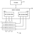
도 2는 3x3 간섭 변조기 디스플레이를 통합하는 전자 디바이스를 예시하는 시스템 블록도의 일 예를 도시한다.
도 3은 도 1의 간섭 변조기에 대한 이동가능 반사층 포지션 대 인가된 전압을 예시하는 다이어그램의 일 예를 도시한다.
도 4는 갖가지 공통 및 세그먼트 전압들이 인가되는 경우에 간섭 변조기의 갖가지 상태들을 예시하는 테이블의 일 예를 도시한다.
도 5a는 도 2의 3x3 간섭 변조기 디스플레이에서의 디스플레이 데이터의 프레임을 예시하는 다이어그램의 일 예를 도시한다.
도 5b는 도 5a에 예시된 디스플레이 데이터의 프레임을 쓰는데 이용될 수도 있는 공통 및 세그먼트 신호들에 대한 타이밍도의 일 예를 도시한다.
도 6a는 도 1의 간섭 변조기 디스플레이의 부분 단면의 일 예를 도시한다.
도 6b-6e는 간섭 변조기들의 가변하는 구현예들의 단면들의 예들을 도시한다.
도 7은 간섭 변조기에 대한 제조 프로세스를 예시하는 흐름도의 일 예를 도시한다.
도 8a-8e는 간섭 변조기를 만드는 방법에서의 여러 가지 스테이지들의 단면 개략도들의 예들을 도시한다.
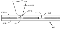
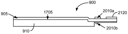
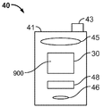
도 9a는 덮개 유리 상에 형성된 센서 전극들의 일 예를 도시한다.
도 9b는 덮개 유리 상에 형성된 센서 전극들의 대안적인 예를 도시한다.
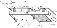
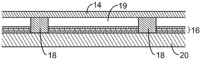
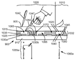
도 10a는 결합형 센서 디바이스의 단면도의 일 예를 도시한다.
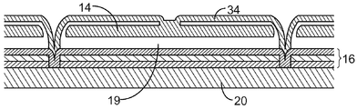
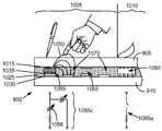
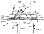
도 10b-10d는 대안적 결합형 센서 디바이스들의 단면도들의 예들을 도시한다.
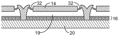
도 11a-11d는 높은 모듈러스 및 낮은 모듈러스 압축가능 층들을 갖는 결합형 센서 디바이스들의 단면도들의 예들을 도시한다.
도 12는 결합식 터치, 필기 및 지문 센서를 갖는 덮개 유리를 구비한 디바이스의 일 예를 도시한다.
도 13은 힘 감응 스위치 구현예의 평면도의 일 예를 도시한다.
도 14는 도 13에 도시된 힘 감응 스위치 구현예의 행을 관통하는 단면의 일 예를 도시한다.
도 15a는 도 13 및 14에 도시된 구현예의 컴포넌트들을 나타내는 회로도의 일 예를 도시한다.
도 15b는 도 13 및 14에 관련된 대안적 구현예의 컴포넌트들을 나타내는 회로도의 일 예를 도시한다.
도 16은 결합형 센서 디바이스에 대한 제조 프로세스를 도시하는 흐름도의 일 예를 도시한다.
도 17a-17d는 도 16의 제조 프로세스의 갖가지 스테이지들 동안에 부분적으로 형성된 결합형 센서 디바이스들의 예들을 도시한다.
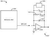
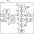
도 18a는 결합형 센서 디바이스의 하이-레벨 아키텍처를 예시하는 블록도의 일 예를 도시한다.
도 18b는 결합형 센서 디바이스에 대한 제어 시스템을 예시하는 블록도의 일 예를 도시한다.
도 18c는 결합형 센서 디바이스에서의 센셀 (sensel) 에 대한 물리적 컴포넌트들 및 그것들의 전기적 등가물들의 일 예의 표현을 도시한다.
도 18d는 결합형 센서 디바이스의 대안적 센셀의 일 예를 도시한다.
도 18e는 결합형 센서 디바이스에서의 센셀의 등가 회로 컴포넌트들을 나타내는 개략도의 일 예를 도시한다.
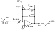
도 18f는 필기 또는 스타일러스 모드 센싱을 위해 구성될 수도 있는 결합형 센서 디바이스를 위한 연산 증폭기 회로의 일 예를 도시한다.
도 18g는 터치 모드 센싱을 위해 구성된 도 18f의 연산 증폭기 회로의 일 예를 도시한다.
도 18h는 클램프 회로를 구비하는 결합형 센서 디바이스를 위한 연산 증폭기 회로의 일 예를 도시한다.
도 18i는 클램프 회로 전달 함수들의 예들을 도시한다.
도 18j는 클램프 회로에 대한 회로도의 일 예를 도시한다.
도 19는 대안적 결합형 센서 디바이스의 일 부분의 단면의 일 예를 도시한다.
도 20은 결합형 센서 디바이스를 위한 라우팅의 평면도의 일 예를 도시한다.
도 21a는 도 20에 도시된 결합형 센서 디바이스를 관통하는 단면도의 일 예를 도시한다.
도 21b는 끝부분이 굽은 (wrap-around) 구현예의 단면의 일 예를 도시한다.
도 22는 지문 기반 사용자 인증 프로세스를 예시하는 흐름도의 일 예를 도시한다.
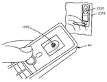
도 23a는 보안형 상거래들을 행하도록 구성될 수도 있는 모바일 디바이스의 일 예를 도시한다.
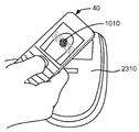
도 23b는 물리적 액세스 애플리케이션들에 대한 지문 보안식 모바일 디바이스의 사용의 일 예를 도시한다.
도 24a는 보안형 태블릿 디바이스의 일 예를 도시한다.
도 24b는 대안적 보안형 태블릿 디바이스의 일 예를 도시한다.
도 25a 및 25b는 결합형 센서 디바이스를 포함하는 디스플레이 디바이스를 예시하는 시스템 블록도들의 예들을 도시한다.
여러 도면들에서의 유사한 참조 번호들 및 지정들은 유사한 엘리먼트들을 나타낸다.1 shows an example of an isometric view depicting two adjacent pixels in a series of pixels of an interference modulator (IMOD) display device.
2 shows an example of a system block diagram illustrating an electronic device incorporating a 3x3 interferometric modulator display.
3 shows an example of a diagram illustrating movable reflective layer position versus applied voltage for the interference modulator of FIG. 1.
4 shows an example of a table illustrating various states of an interference modulator when various common and segment voltages are applied.
FIG. 5A shows an example of a diagram illustrating a frame of display data in the 3x3 interferometric modulator display of FIG. 2.
FIG. 5B shows an example of a timing diagram for common and segment signals that may be used to write the frame of display data illustrated in FIG. 5A.
6A shows an example of a partial cross section of the interference modulator display of FIG. 1.
6B-6E show examples of cross sections of varying implementations of interferometric modulators.
7 shows an example of a flow diagram illustrating a manufacturing process for an interferometric modulator.
8A-8E show examples of cross-sectional schematics of various stages in a method of making an interference modulator.
9A shows an example of sensor electrodes formed on a cover glass.
9B shows an alternative example of sensor electrodes formed on the cover glass.
10A shows an example of a cross-sectional view of a coupled sensor device.
10B-10D show examples of cross-sectional views of alternative coupled sensor devices.
11A-11D show examples of cross-sectional views of coupled sensor devices having high modulus and low modulus compressible layers.
12 shows an example of a device with a cover glass having a combined touch, writing and fingerprint sensor.
13 shows an example of a top view of a force sensitive switch implementation.
FIG. 14 shows an example of a cross section through a row of the force sensitive switch implementation shown in FIG. 13.
15A shows an example of a circuit diagram illustrating components of the implementation shown in FIGS. 13 and 14.
FIG. 15B shows an example of a circuit diagram showing components of an alternative implementation related to FIGS. 13 and 14.
16 shows an example of a flow diagram illustrating a manufacturing process for a coupled sensor device.
17A-17D show examples of coupled sensor devices partially formed during the various stages of the manufacturing process of FIG. 16.
18A shows an example of a block diagram illustrating a high-level architecture of a coupled sensor device.
18B shows an example of a block diagram illustrating a control system for a coupled sensor device.
18C shows an example representation of physical components and their electrical equivalents for a sensel in a coupled sensor device.
18D shows an example of an alternative sensel of a coupled sensor device.
18E shows an example of a schematic diagram illustrating equivalent circuit components of a sensel in a coupled sensor device.
18F shows an example of an operational amplifier circuit for a coupled sensor device that may be configured for handwriting or stylus mode sensing.
18G illustrates an example of the operational amplifier circuit of FIG. 18F configured for touch mode sensing.
18H shows an example of an operational amplifier circuit for a coupled sensor device having a clamp circuit.
18I shows examples of clamp circuit transfer functions.
18J shows an example of a circuit diagram for a clamp circuit.
19 shows an example of a cross section of a portion of an alternative coupled sensor device.
20 shows an example of a top view of routing for a coupled sensor device.
FIG. 21A shows an example of a cross-section through the coupled sensor device shown in FIG. 20.
21B shows an example of a cross section of a wrap-around embodiment.
22 shows an example of a flow diagram illustrating a fingerprint based user authentication process.
23A illustrates an example of a mobile device that may be configured to conduct secure commerce.
23B shows an example of the use of a fingerprint secure mobile device for physical access applications.
24A illustrates an example of a secure tablet device.
24B shows an example of an alternative secure tablet device.
25A and 25B show examples of system block diagrams illustrating a display device that includes a coupled sensor device.
Like reference numbers and designations in the various drawings indicate like elements.
다음의 설명은 본 개시물의 혁신적 양태들을 설명할 목적을 위한 특정한 구현예들을 지향한다. 그러나, 이 기술분야의 통상의 기술을 가진 자는 본원에서의 교시들이 수많은 상이한 방법들에 적용될 수 있다는 것을 쉽사리 인식할 것이다. 설명되는 구현예들은 이미지를, 동작 (예컨대, 비디오) 이든 또는 정지 (예컨대, 스틸 이미지) 이든, 그리고 텍스트형이든, 그래픽이든 또는 그림이든 디스플레이하도록 구성될 수 있는 임의의 디바이스 또는 시스템으로 구현될 수도 있다. 더 상세하게는, 설명되는 구현예들은, 모바일 전화기들, 멀티미디어 인터넷 가능 (enabled) 셀룰러 전화기들, 모바일 텔레비전 수신기들, 무선 디바이스들, 스마트폰들, Bluetooth® 디바이스들, 개인휴대 정보단말들 (PDA들), 무선 전자 메일 수신기들, 핸드헬드 또는 휴대용 컴퓨터들, 넷북들, 노트북들, 스마트북들, 테블릿들, 프린터들, 복사기들, 스캐너들, 팩시밀리 디바이스들, GPS 수신기들/네비게이터들, 카메라들, MP3 플레이어들, 캠코더들, 게임 콘솔들, 손목시계들, 클록들, 계산기들, 텔레비전 모니터들, 평판 디스플레이들, 전자 판독 디바이스들 (즉, e-리더들), 컴퓨터 모니터들, 오토 디스플레이들 (오도미터 (odometer) 및 속도계 디스플레이들 등을 포함함), 조종석 컨트롤들 (cockpit controls) 및/또는 디스플레이들, 카메라 뷰 디스플레이들 (이를테면 차량에서의 후방 카메라 (rear view camera) 의 디스플레이), 전자 사진들, 전자 광고판들 및 표지판들, 프로젝터들, 건축 구조물들, 전자레인지들 (microwaves), 냉장고들, 스테레오 시스템들, 카세트 레코더들 또는 플레이어들, DVD 플레이어들, CD 플레이어들, VCR들, 라디오들, 휴대용 메모리 칩들, 세탁기들, 드라이어들, 세탁기/건조기들, 주차 미터기들, 패키징 (이를테면 전기기계 시스템들, 마이크로전자기계 시스템들, 및 비-MEMS 애플리케이션들에서의 패키징), 미적 구조들 (예컨대, 한 점의 보석류에 대한 이미지들의 디스플레이) 및 다양한 EMS 디바이스들과 같은 것들이지만 그것들로 제한되지 않는 다양한 전자 디바이스들에 포함될 수도 있거나 또는 그런 전자 디바이스들에 연관될 수도 있다는 것이 의도된다. 본원에서의 교시들은 또한 전자 스위칭 디바이스들, 무선 주파수 필터들, 센서들, 가속도계들, 자이로스코프들, 움직임 센싱 디바이스들, 자력계들, 소비자 가전기기들을 위한 관성 컴포넌트들, 소비자 가전기기 제품들의 부품들, 버렉터들 (varactors), 액정 디바이스들, 전기영동 디바이스들, 드라이브 체계들, 제조 프로세스들 및 전자 테스트 장비와 같은 것들이지만 그것들로 제한되지는 않는 비-디스플레이 애플리케이션들에서 사용될 수 있다. 따라서, 그 교시들은 도면들에서 단독으로 묘사된 구현예들로 제한되도록 의도되지는 않고, 대신 이 기술분야의 통상의 지식을 가진자에게 쉽사리 명백할 바와 같이 넓은 적용 가능성을 가진다.The following description is directed to specific implementations for the purpose of describing innovative aspects of the present disclosure. However, one of ordinary skill in the art will readily recognize that the teachings herein can be applied to a number of different methods. The described embodiments may be implemented in any device or system that can be configured to display an image, whether it is motion (eg, video) or still (eg, a still image), and whether it is textual, graphical, or picture. have. More specifically, the described implementations include mobile telephones, multimedia internet enabled cellular telephones, mobile television receivers, wireless devices, smartphones, Bluetooth® devices, personal digital assistants (PDAs). Wireless e-mail receivers, handheld or portable computers, netbooks, notebooks, smartbooks, tablets, printers, copiers, scanners, facsimile devices, GPS receivers / navigators, Cameras, MP3 players, camcorders, game consoles, watches, clocks, calculators, television monitors, flat panel displays, electronic reading devices (ie e-readers), computer monitors, auto Displays (including odometer and speedometer displays, etc.), cockpit controls and / or displays, camera view displays (such as a vehicle) Display of rear view camera), electronic photos, electronic billboards and signs, projectors, building structures, microwaves, refrigerators, stereo systems, cassette recorders or player , DVD players, CD players, VCRs, radios, portable memory chips, washing machines, dryers, washing machines / dryers, parking meters, packaging (such as electromechanical systems, microelectromechanical systems, and Packaging in non-MEMS applications), aesthetic structures (eg, display of images for a piece of jewelry) and various EMS devices, such as, but not limited to, various electronic devices. It is intended that it may be associated with electronic devices. The teachings herein also include electronic switching devices, radio frequency filters, sensors, accelerometers, gyroscopes, motion sensing devices, magnetometers, inertial components for consumer electronics, components of consumer electronics products. Can be used in non-display applications such as, but not limited to, varactors, liquid crystal devices, electrophoretic devices, drive schemes, manufacturing processes and electronic test equipment. Thus, the teachings are not intended to be limited to the implementations depicted alone in the figures, but instead have broad applicability, as will be readily apparent to those skilled in the art.
본원에서 설명되는 일부 구현예들은 필기 입력을 위한 스타일러스 검출, 지문 영상화, 및 터치 센싱을 위한 정전용량식 및 저항식 기술들의 신규한 양태들을 결합한다. 일부 이러한 구현예들은, 결합형 센서 디바이스의 적어도 부분이 디스플레이 상에 오버레이될 수도 있거나 또는 그렇지 않으면 디스플레이와 결합될 수도 있는 덮개 유리 장치 내에 통합된, 그 결합형 센서 디바이스를 제공한다. 덮개 유리 장치는 2, 3 또는 그 이상의 층들을 가질 수도 있다. 일부 구현예들에서, 덮개 유리 장치는 실질적으로 투명한 및 유연한 (flexible) 상부 기판과 실질적으로 투명한 및 상대적으로 더 단단한 하부 기판을 구비한다. 일부 이런 구현예들에서, 덮개 유리 장치의 하부 기판은 디스플레이 기판 상에 오버레이될 수도 있다. 대안적 구현예들에서, 덮개 유리 장치의 하부 기판은 디스플레이 기판일 수도 있다. 예를 들어, 덮개 유리 장치의 하부 기판은 IMOD 디바이스들이, 아래에서 설명되는 바와 같이 그 위에 제작되는 동일한 투명 기판일 수도 있다.Some implementations described herein combine novel aspects of capacitive and resistive techniques for stylus detection, fingerprint imaging, and touch sensing for handwriting input. Some such implementations provide such a coupled sensor device, integrated in a lid glass apparatus, wherein at least a portion of the coupled sensor device may be overlaid on the display or otherwise combined with the display. The lid glass apparatus may have two, three or more layers. In some embodiments, the lid glass device has a substantially transparent and relatively harder bottom substrate and a substantially transparent and relatively harder bottom substrate. In some such implementations, the bottom substrate of the lid glass apparatus may be overlaid on the display substrate. In alternative implementations, the lower substrate of the lid glass apparatus may be a display substrate. For example, the bottom substrate of the lid glass apparatus may be the same transparent substrate on which the IMOD devices are fabricated thereon, as described below.
이러한 센서 디바이스들의 갖가지 구현예들이 여기서 설명된다. 일부 구현예들에서, 디스플레이 디바이스의 덮개 유리는 단일 또는 다중 터치 센서로서, 필기 (또는 노트 캡처) 입력 디바이스로서, 그리고 지문 센서로서 역할을 한다. 센서 기능성과 해상도는 덮개 유리 상의 특정 로케이션들에 맞춤될 수 있다. 일부 이런 구현예들에서, 지문 센싱 엘리먼트들이 위치되는 영역은 지문 검출뿐만 아니라, 필기 및 터치 기능성도 제공할 수도 있다. 일부 다른 구현예들에서, 지문 센서는 지문 기능성만을 제공하는 별도의 고해상도 구역으로 분리될 수도 있다. 일부 구현예들에서, 센서 디바이스는 결합식 터치 및 스타일러스 입력 디바이스로서 역할을 한다. 제작의 갖가지 방법들이 여기서 설명되며, 뿐만 아니라 결합형 센서 디바이스를 구비하는 디바이스를 사용하기 위한 방법들이 설명된다.Various implementations of such sensor devices are described herein. In some implementations, the lid glass of the display device serves as a single or multiple touch sensor, as a writing (or note capturing) input device, and as a fingerprint sensor. Sensor functionality and resolution can be tailored to specific locations on the lid glass. In some such implementations, the area where the fingerprint sensing elements are located may provide not only fingerprint detection but also handwriting and touch functionality. In some other implementations, the fingerprint sensor may be separated into a separate high resolution zone that provides only fingerprint functionality. In some implementations, the sensor device serves as a combined touch and stylus input device. Various methods of fabrication are described herein, as well as methods for using a device having a coupled sensor device.
이 개시물에서 설명되는 주제의 특정 구현예들은 다음의 잠재적 이점들 중 하나 이상을 실현하기 위해 구현될 수 있다. 본원에서 설명되는 일부 구현예들은 터치 센싱, 필기 입력 및 일부 경우들에서는 지문 영상화를 위한 정전용량식 및 저항식 기술들의 양태들을 결합한다. 일부 이러한 구현예들은 디스플레이 상에 오버레이될 수 있는 다기능 사용자 입력 센서를 인에이블시키기 위해 정전용량식 및 저항식 기술들을 결합시키는 터치 센서를 제공한다. 결합형 센서 디바이스의 일부 구현예들은 덮개 유리와 일부 기존의 투영 정전용량식 터치 (projected capacitive touch; PCT) 기반 디바이스들에서의 디스플레이 유리 사이에 배치되는 중간 터치 센서 층을 제거한다. 따라서, 일부 이러한 구현예들은 PCT 및 저항식 기술들의 적어도 일부 단점들을 완화시키거나 또는 제거할 수 있다.Particular implementations of the subject matter described in this disclosure can be implemented to realize one or more of the following potential advantages. Some implementations described herein combine aspects of capacitive and resistive techniques for touch sensing, handwriting input, and in some cases fingerprint imaging. Some such embodiments provide a touch sensor that combines capacitive and resistive technologies to enable a multifunction user input sensor that can be overlaid on a display. Some implementations of the combined sensor device eliminate the intermediate touch sensor layer disposed between the cover glass and the display glass in some existing projected capacitive touch (PCT) based devices. Thus, some such implementations can mitigate or eliminate at least some disadvantages of PCT and resistive technologies.
하이브리드 PCT 및 디지털 저항식 터치 (digital resistive touch; DRT) 구현예는, 예를 들어, 좁은 스타일러스 선단이 디스플레이 상을 누르는 것을 DRT 양태로 검출하면서 또한 손가락으로 디스플레이 위를 매우 가볍게 브러싱 (brushing) 또는 가깝게 호버링 (hovering) 하는 것을 PCT 양태를 이용하여 검출하는 것을 허용한다. 센서 디바이스는 스타일러스 또는 펜 입력의 임의의 형태를 그것이 도전성이든 또는 비도전성이든 상관없이 수용할 수도 있다. 투명한 또는 사실상 (effectively) 투명한 힘 감응 저항기들은 광학적 및 전기적 성능을 개선하기 위해 센셀들의 일부 또는 전부 내에 포함될 수도 있다.Hybrid PCT and digital resistive touch (DRT) implementations, for example, detect the pressing of a narrow stylus tip on the display in a DRT mode while also very lightly brushing or close to the display with a finger. Allow to detect hovering using the PCT aspect. The sensor device may accept any form of stylus or pen input whether it is conductive or non-conductive. Transparent or effectively transparent force sensitive resistors may be included in some or all of the sensing cells to improve optical and electrical performance.
일부 구현예들에 따르면, 결합 센서는 2 이상의 패턴화된 층들을 구비할 수도 있으며, 그 층들 중 일부는 다른 기판 상에 있을 수도 있다. 상부 (또는 바깥쪽) 기판은, 예를 들어, 폴리에틸렌 테레프탈레이트 (PET), 폴리에틸렌 나프탈레이트 (PEN), 폴리이미드, 또는 유사한 재료와 같은 플라스틱으로 형성될 수도 있다. 상부 기판은 또한 실질적으로 투명할 수도 있고 그것의 아래쪽에 패턴화된 인듐 주석 산화물 (ITO) 과 같은 실질적으로 투명한 도전체를 가질 수도 있다. 하부 기판은 실질적 투명 기판 재료, 이를테면 유리로, 또 다른 적합한 재료와 함께 형성될 수도 있다. 실질적 투명 기판의 상단 표면은 ITO와 같은 실질적으로 투명한 도전체 재료의 패턴화된 층일 수도 있다. 일부 구현예들에서, 상부 기판의 아래쪽 및 하부 기판의 상부 쪽의 도전체들은 2 개의 상이한 층들의 각각 상에서 행들 또는 열들로서 접속된 마름모꼴 형상 전극들로 패턴화될 수도 있다.According to some embodiments, the coupling sensor may have two or more patterned layers, some of which may be on another substrate. The upper (or outer) substrate may be formed of plastic such as, for example, polyethylene terephthalate (PET), polyethylene naphthalate (PEN), polyimide, or similar materials. The upper substrate may also be substantially transparent and may have a substantially transparent conductor such as patterned indium tin oxide (ITO) beneath it. The lower substrate may be formed of a substantially transparent substrate material, such as glass, with another suitable material. The top surface of the substantially transparent substrate may be a patterned layer of substantially transparent conductor material such as ITO. In some implementations, the conductors below the top substrate and the top side of the bottom substrate may be patterned with rhombic shaped electrodes connected as rows or columns on each of the two different layers.
일부 이러한 구현예들은, 센서 디바이스의 유연한 상부 기판이 신호선들, 전기 접지, 및 전력의 라우팅을 허용하기 위해 연장된 부분 상에 패턴화된 금속화물을 가지는, 끝부분이 굽은 구성을 포함한다. 이 유연한 상부 기판은 덮개 유리 장치의 상대적으로 더 단단한 하부 기판의 에지를 에워쌀 수도 있다. 접속용 소켓들을 구비한 하나 이상의 IC들 또는 패시브 컴포넌트들은 비용 및 복잡도를 줄이기 위해 유연한 층 상에 장착될 수도 있다. 하부 기판 상의 센서 전극들을 어드레싱하는 신호선들은 유연한 상부 기판의 아래쪽에서 대응하는 패턴들에 라우팅되고 접속될 수도 있다. 이런 구현예들은 상부 층의 신호선들을 집적회로들 및/또는 다른 디바이스들에 전기 접속시키기 위한 플렉스 케이블에 대한 필요를 없애는 잠재적 이점을 가진다. 그 접근법은 최종 덮개 유리 장치의 일부 버전들에 베젤 없는 구성을 허용한다.Some such implementations include a bent configuration in which the flexible top substrate of the sensor device has a patterned metallization on the extended portion to allow signal lines, electrical ground, and routing of power. This flexible top substrate may surround the edge of the relatively harder bottom substrate of the lid glass device. One or more ICs or passive components with connecting sockets may be mounted on a flexible layer to reduce cost and complexity. Signal lines addressing the sensor electrodes on the lower substrate may be routed and connected to corresponding patterns on the underside of the flexible upper substrate. Such implementations have the potential advantage of eliminating the need for a flex cable to electrically connect the signal lines of the top layer to integrated circuits and / or other devices. The approach allows for a bezelless configuration in some versions of the final lid glass arrangement.
제작 방법들은 밑에 있는 디스플레이들의 광학적 성능을 증가시키는 대부분의 투명한 기판들 및 재료들을 포함한다. 그 제작 프로세스들은 센서 디바이스의 적어도 일 부분을 위해 유연한 기판들을 활용할 수도 있고, 그것들을 저 비용을 위해 롤 투 롤 (roll-to-roll) 프로세싱에 제공할 수도 있다.Fabrication methods include most transparent substrates and materials that increase the optical performance of underlying displays. The fabrication processes may utilize flexible substrates for at least a portion of the sensor device and provide them for roll-to-roll processing for low cost.
결합 센서의 상부 및 하부 부분들 사이의 유연한 (compliant), 탄성중합체 층의 사용은 스타일러스로부터 가해진 압력 또는 힘에 대한 민감도를 증가시키면서도, 주어진 센셀 피치에 대한 측방향 해상도를 증가시킬 수 있다. 탄성중합체 재료는 힘 감응 저항기들의 포함을 위한 개방 지역들을 포함할 수도 있다. 탄성중합체 및 FSR 재료들의 신중한 선택으로, 에어 갭들에 수반될 수 있는 투과율의 손실은 최소화된다.The use of a compliant, elastomeric layer between the upper and lower portions of the coupling sensor can increase the lateral resolution for a given sensor pitch while increasing the sensitivity to pressure or force exerted from the stylus. The elastomeric material may include open areas for the inclusion of force sensitive resistors. With careful selection of elastomers and FSR materials, the loss of transmission that can accompany air gaps is minimized.
힘 감응 스위치들 및 로컬 커패시터들의 어레이는 로컬 커패시터를 연관된 PCT 검출 회로에 접속시키기 위해 사용될 수도 있으며, 여기서 각각의 커패시터는 힘 감응 스위치가 스타일러스 또는 손가락의 누름에 의해 폐쇄되는 경우에 높은 커패시턴스 증가를 달성하기 위해 얇은 유전체 층으로 형성된다. 동일한 PCT 검출 회로는 그러므로 손가락으로 터치된 경우 (터치 모드) 의 상호 커패시턴스에서의 변화들 및 감응 스위치가 눌러지는 경우 (스타일러스 또는 지문 모드) 의 센셀 커패시턴스에서의 변화들을 검출하는데 사용될 수 있다.An array of force sensitive switches and local capacitors may be used to connect the local capacitor to the associated PCT detection circuit, where each capacitor achieves a high capacitance increase when the force sensitive switch is closed by stylus or finger press. To form a thin dielectric layer. The same PCT detection circuit can therefore be used to detect changes in mutual capacitance when touched by a finger (touch mode) and changes in sense capacitance when the sensitive switch is pressed (stylus or fingerprint mode).
결합형, 다기능 센서 디바이스는 필기 입력 및 지문 인식과 같은 부가적인 기능들을 수행하도록 단일 터치스크린을 인에이블시킨다. 일부 구현예들에서, 이들 다수의 특징들은 사용자 인증을 통한 증가된 보안을 허용하고, 필기의 양호한 캡처 및 사용자 인터페이스들에 대한 더 상호작용적인 접근법을 허용한다. 센서 디바이스를 갖는 셀 전화기와 같은 핸드헬드 모바일 디바이스는, 거래들(transactions) 및 물리적 액세스를 가능하게 하기 위해 사용자 인증에 대한 게이트웨이로서 모바일 디바이스를 사용하는 것; 거래 애플리케이션들에 대한 시그너쳐 인식 및 전송을 위해 필기 입력 기능을 사용하는 것; 및 학교 설정환경 (setting) 에서의 학생들 또는 회사 설정환경에서의 고용인들의 노트들 및 다른 문서들을 자동으로 캡처하기 위해 필기 입력 특징을 이용하는 것을 포함한, 애플리케이션들의 어레이를 가능하게 할 수 있다.The combined, multifunction sensor device enables a single touchscreen to perform additional functions such as handwriting input and fingerprint recognition. In some implementations, these multiple features allow for increased security through user authentication and allow for better capture of handwriting and a more interactive approach to user interfaces. Handheld mobile devices, such as cell phones with sensor devices, include using the mobile device as a gateway for user authentication to enable transactions and physical access; Using handwriting input functionality for signature recognition and transmission for trading applications; And using a handwriting input feature to automatically capture notes and other documents of students in a school setting or employees in a company setting.
일부 이런 구현예들에서, 별개의 제어기가 센서 디바이스를 위해 구성될 수도 있거나, 또는 그 제어기는 애플리케이션들 프로세서의 부분으로서 포함될 수도 있다. 필기, 터치 및 지문 검출을 위한 소프트웨어는 하나 이상의 제어기들 또는 애플리케이션들의 프로세서에 포함될 수도 있다. 저, 중 및 고 해상도는 센셀들의 서브세트를 스캐닝함으로써, 또는 라인들 또는 열들을 총합함으로써 단일 센서 디바이스로 획득될 수 있다. 소비 전력은 제어기를 사용하여 센서 화소들 (또는 행들 또는 열들) 을 전기적으로 총합함으로써 감소될 수도 있어서, 센서 화소들은 더 큰 어레이를 갖는 더 높은 해상도가 필요하기까지 저 전력 소형 어레이로서 기능을 한다. 소비 전력은 센서 디바이스의 부분들 또는 전부를 턴 오프, 제어기의 부분들을 턴 오프, 또는 감소된 프레임 레이트에서 제 1-레벨 스크리닝을 채용함으로써 감소될 수도 있다. 일부 이런 구현예들에서, 결합식 PCT 센서 및 디지털 저항식 터치 (DRT) 센서는 커패시터들 (PCT) 의 패시브 어레이 및 저항식 스위치들 (DRT) 의 패시브 어레이를 가진다. 터치 센서 및 스타일러스 센서 시스템들이 일반적으로 상이한 센싱 기법들을 사용하지만, 공통 구조를 갖는 홀리스틱 접근법은 PCB 부품 수를 절약하며, ASIC 구현물에서의 면적을 감소시키며, 전력을 감소시키고, 터치 및 스타일러스 서브시스템들 간의 절연에 대한 필요성을 없앤다.In some such implementations, a separate controller may be configured for the sensor device, or the controller may be included as part of the applications processor. Software for handwriting, touch, and fingerprint detection may be included in the processor of one or more controllers or applications. Low, medium, and high resolution can be obtained with a single sensor device by scanning a subset of the sensing cells, or by summing lines or columns. Power consumption may be reduced by electrically summing sensor pixels (or rows or columns) using a controller, such that the sensor pixels function as a low power small array until a higher resolution with a larger array is needed. Power consumption may be reduced by turning off portions or all of the sensor device, turning off portions of the controller, or employing first-level screening at a reduced frame rate. In some such implementations, the combined PCT sensor and the digital resistive touch (DRT) sensor have a passive array of capacitors (PCT) and a passive array of resistive switches (DRT). While touch sensor and stylus sensor systems typically use different sensing techniques, a holistic approach with a common structure saves PCB component count, reduces area in ASIC implementations, reduces power, touch and stylus subsystems. Eliminates the need for liver isolation
설명되는 구현예들이 적용될 수도 있는 적합한 EMS 또는 MEMS 디바이스의 일 예는, 반사형 디스플레이 디바이스이다. 반사형 디스플레이 디바이스들은 입사하는 광을 광 간섭의 원리들을 이용하여 선택적으로 흡수 및/또는 반사하는 간섭 변조기들 (IMOD들) 을 통합할 수도 있다. IMOD들은 흡수체, 그 흡수체에 대해 이동가능한 것인 반사체, 그리고 흡수체 및 반사체 사이에서 규정된 광학적 공진 공동을 구비할 수 있다. 반사체는 둘 이상의 상이한 포지션들로 움직일 수 있으며, 그것은 광학적 공진 공동의 사이즈를 변화시킬 수 있고 이에 의해 간섭 변조기의 반사율에 영향을 미친다. IMOD들의 반사율 스펙트럼들은 상이한 컬러들을 생성하도록 가시 파장들 전체에 걸쳐 시프트될 수 있는 상당히 넓은 스펙트럼 대역들을 생성할 수 있다. 스펙트럼 대역의 포지션은 광학적 공진 공동의 두께를 변경함으로써 조절될 수 있다. 광학적 공진 공동을 변화시키는 하나의 방법은 반사체의 포지션을 변화시키는 것이다.One example of a suitable EMS or MEMS device to which the described embodiments may apply is a reflective display device. Reflective display devices may incorporate interference modulators (IMODs) that selectively absorb and / or reflect incident light using the principles of optical interference. IMODs can have an absorber, a reflector that is movable relative to the absorber, and an optical resonant cavity defined between the absorber and the reflector. The reflector can move in two or more different positions, which can change the size of the optical resonant cavity, thereby affecting the reflectance of the interferometric modulator. Reflectance spectra of IMODs can produce fairly wide spectral bands that can be shifted across visible wavelengths to produce different colors. The position of the spectral band can be adjusted by changing the thickness of the optical resonant cavity. One way to change the optical resonant cavity is to change the position of the reflector.
도 1은 간섭 변조기 (IMOD) 디스플레이 디바이스의 일련의 화소들에서의 2개의 인접 화소들을 묘사하는 등각투상도의 일 예를 도시한다. IMOD 디스플레이 디바이스는 하나 이상의 간섭형 MEMS 디스플레이 엘리먼트들을 구비한다. 이들 디바이스들에서, MEMS 디스플레이 엘리먼트들의 화소들은 밝거나 또는 어두운 상태일 수 있다. 밝은 ("이완된 (relaxed)", "개방" 또는 "온") 상태에서, 디스플레이 엘리먼트는 입사 가시광선의 큰 부분을, 예컨대, 사용자에게 반사한다. 반대로, 어두운 ("작동된 (actuated)", "폐쇄된" 또는 "오프") 상태에서, 디스플레이 엘리먼트는 입사 가시광선을 거의 반사하지 않는다. 일부 구현예들에서, 온 및 오프 상태들의 광 반사율 특성들은 역전될 수도 있다. MEMS 화소들은 흑색 및 백색 외에도 컬러 디스플레이를 허용하는 특정 파장들에서 주로 반사하도록 구성될 수 있다.1 shows an example of an isometric view depicting two adjacent pixels in a series of pixels of an interference modulator (IMOD) display device. The IMOD display device has one or more interfering MEMS display elements. In these devices, the pixels of the MEMS display elements may be bright or dark. In the bright ("relaxed", "open" or "on") state, the display element reflects a large portion of the incident visible light, for example to the user. In contrast, in the dark (“actuated”, “closed” or “off”) state, the display element reflects little incident visible light. In some implementations, the light reflectance characteristics of the on and off states may be reversed. MEMS pixels can be configured to reflect primarily at certain wavelengths that allow color display in addition to black and white.
IMOD 디스플레이 디바이스는 IMOD들의 행/열 어레이를 구비할 수 있다. 각각의 IMOD는, 에어 갭 (광학적 갭 또는 공동이라고도 지칭됨) 을 형성하기 위해 서로로부터 가변 및 제어가능 거리에 위치된 한 쌍의 반사층들, 즉, 이동가능 반사층 및 고정된 부분 반사층을 포함할 수 있다. 이동가능 반사층은 적어도 2개의 포지션들 사이를 움직일 수도 있다. 제 1 포지션, 즉, 이완된 포지션에서, 이동가능 반사층은 고정된 부분 반사층으로부터 비교적 큰 거리에 위치될 수 있다. 제 2 포지션, 즉, 작동된 포지션에서, 이동가능 반사층은 부분 반사층에 더 가까이 위치될 수 있다. 2 개의 층들로부터 반사하는 입사 광은 이동가능 반사층의 포지션에 의존하여 보강적으로 또는 상쇄적으로 간섭하여, 각각의 화소에 대해 전체의 반사 또는 비-반사 상태를 생성할 수 있다. 일부 구현예들에서, IMOD는 작동되지 않은 경우에 반사 상태에 있어, 가시 스펙트럼 내의 광을 반사할 수도 있고, 작동되지 않은 경우에 어두운 상태에 있어, 가시 범위 내의 광을 흡수 및/또는 상쇄적으로 간섭할 수도 있다. 일부 다른 구현예들에서, 그러나, IMOD는 작동되지 않은 경우에 어두운 상태, 그리고 작동된 경우에 반사 상태에 있을 수도 있다. 일부 구현예들에서, 인가된 전압의 도입은 상태들을 변화시키기 위해 화소들을 구동시킬 수 있다. 일부 다른 구현예들에서, 인가된 전하는 상태들을 변화시키기 위해 화소들을 구동시킬 수 있다.The IMOD display device can have a row / column array of IMODs. Each IMOD may include a pair of reflective layers located at variable and controllable distances from each other, ie a movable reflective layer and a fixed partially reflective layer, to form an air gap (also referred to as an optical gap or cavity). have. The movable reflective layer may move between at least two positions. In the first position, ie relaxed position, the movable reflective layer can be located at a relatively large distance from the fixed partial reflective layer. In the second position, ie the activated position, the movable reflective layer can be located closer to the partial reflective layer. Incident light reflecting from the two layers may interfere constructively or destructively depending on the position of the movable reflective layer, creating a totally reflective or non-reflective state for each pixel. In some implementations, the IMOD may be in a reflective state when not in operation, reflecting light in the visible spectrum, and in a dark state when not in operation, absorbing and / or offsetting light in the visible range. It may interfere. In some other implementations, however, the IMOD may be in a dark state when not in operation and in a reflective state when in operation. In some implementations, the introduction of an applied voltage can drive the pixels to change states. In some other implementations, the applied charge can drive the pixels to change states.
도 1에서의 화소 어레이의 묘사된 부분은 2 개의 인접한 간섭 변조기들 (12) (즉, IMOD 화소들) 을 포함한다. 왼쪽의 (예시된 대로의) IMOD (12) 에서, 이동가능 반사층 (14) 은 부분 반사층을 포함하는 광학적 스택 (16) 으로부터 어떤 거리 (이것은 설계 파라미터들에 기초하여 미리 결정될 수도 있음) 에서 이완된 포지션으로 예시된다. 왼쪽의 IMOD (12) 에 걸리게 인가된 전압 V0은 이동가능 반사층 (14) 의 작동을 유발하는데 불충분하다. 오른쪽의 IMOD (12) 에서, 이동가능 반사층 (14) 은 광학적 스택 (16) 가까이 있는, 인접한 또는 접하는 작동된 포지션으로 예시된다. 오른쪽의 IMOD (12) 에 걸리게 인가된 전압 Vbias는 이동가능 반사층 (14) 을 이동시키기에 충분하고 그 이동가능 반사층을 작동된 포지션에서 유지할 수 있다.The depicted portion of the pixel array in FIG. 1 includes two adjacent interference modulators 12 (ie IMOD pixels). In the left IMOD 12 (as illustrated), the movable
도 1에서, 화소들 (12) 의 반사 특성들은 화소들 (12) 에 입사하는 광을 나타내는 화살표 (13), 및 왼쪽의 화소 (12) 로부터 반사하는 광 (15) 으로 일반적으로 예시된다. 이 기술분야의 통상의 기술을 가진 자는 화소들 (12) 에 입사하는 광 (13) 의 대부분이 투명 기판 (20) 을 통해, 광학적 스택 (16) 쪽으로 투과될 수도 있다는 것을 쉽사리 인식할 것이다. 광학적 스택 (16) 에 입사하는 광의 일 부분은 광학적 스택 (16) 의 부분 반사층을 통해 투과될 수도 있고, 일 부분은 투명 기판 (20) 을 통해 되반사될 것이다. 광학적 스택 (16) 을 통해 투과되는 광 (13) 의 부분은 이동가능 반사층 (14) 에서, 투명 기판 (20) 쪽으로 (을 통해) 되 반사될 수도 있다. 광학적 스택 (16) 의 부분 반사층으로부터 반사된 광 및 이동가능 반사층 (14) 으로부터 반사된 광 사이의 (보강적 또는 상쇄적) 간섭은 화소 (12) 로부터 반사된 광 (15) 의 파장(들)을 결정할 것이다.In FIG. 1, the reflection characteristics of the
광학적 스택 (16) 은 단일 층 또는 여러 층들을 포함할 수 있다. 그 층(들) 은 전극 층, 부분 반사성 및 부분 투과성 층 및 투명 유전체 층 중 하나 이상을 포함할 수 있다. 일부 구현예들에서, 광학적 스택 (16) 은 도전성이며, 부분적으로 투과성이고 부분적으로 반사성이며, 그리고, 예를 들어, 위의 층들의 하나 이상을 투명 기판 (20) 상에 퇴적함으로써 제작될 수도 있다. 전극 층은 다양한 재료들, 이를테면 갖가지 금속들, 예를 들어 인듐 주석 산화물 (ITO) 로 형성될 수 있다. 부분 반사층은 부분적으로 반사성인 다양한 재료들, 이를테면 갖가지 금속들, 이를테면 크롬 (Cr), 반도체들, 및 유전체들로 형성될 수 있다. 부분 반사층은 재료들의 하나 이상의 층들로 형성될 수 있고, 층들의 각각은 단일 재료 또는 재료들의 조합으로 형성될 수 있다. 일부 구현예들에서, 광학적 스택 (16) 은 광학적 흡수체 및 도전체 둘 다로서 역할을 하는 단일 반투명한 두께의 금속 또는 반도체를 포함할 수 있는 한편, (예컨대, 광학적 스택 (16) 의 또는 IMOD의 다른 구조들의) 상이한, 더 큰 도전성 층들 또는 부분들은 IMOD 화소들 사이에서 신호들을 전달하도록 기능할 수 있다. 광학적 스택 (16) 은 또한 하나 이상의 도전성 층들 또는 도전성/광학적 흡수층을 덮는 하나 이상의 절연성 또는 유전체 층들을 포함할 수 있다.
일부 구현예들에서, 광학적 스택 (16) 의 층(들)은 평행한 스트립들로 패턴화될 수 있고, 아래에서 더 설명되는 바와 같이 디스플레이 디바이스에서의 행 전극들을 형성할 수도 있다. 이 기술분야의 통상의 지식을 가진 자에 의해 이해될 바와 같이, 용어 "패턴화된"은 본원에서는 마스킹 뿐만 아니라 에칭 프로세스들을 지칭하는데 이용된다. 일부 구현예들에서, 높은 도전성 및 반사성 재료, 이를테면 알루미늄 (Al) 은, 이동가능 반사층 (14) 을 위해 사용될 수도 있고, 그리고 이들 스트립들은 디스플레이 디바이스에서 열 전극들을 형성할 수도 있다. 이동가능 반사층 (14) 은 포스트들 (18) 의 상단에 퇴적된 열들 및 포스트들 (18) 사이에 퇴적된 개재 희생 재료를 형성하기 위해 (광학적 스택 (16) 의 행 전극들에 직교하는) 퇴적된 금속 층 또는 층들의 일련의 평행한 스트립들로서 형성될 수도 있다. 희생 재료가 식각 제거되는 경우, 규정된 갭 (19), 또는 광학적 공동이, 이동가능 반사층 (14) 및 광학적 스택 (16) 사이에 형성될 수 있다. 일부 구현예들에서, 포스트들 (18) 사이의 간격 (spacing) 은 대략 1 - 1000 ㎛일 수도 있는 반면, 갭 (19) 은 대략 10,000 옹스트롬 (Å) 미만일 수도 있다.In some implementations, the layer (s) of the
일부 구현예들에서, IMOD의 각각의 화소는, 작동된 상태이든 또는 이완된 상태이든, 근본적으로는 고정된 및 가동 (moving) 반사층들 사이에 형성된 커패시터이다. 전압이 인가되지 않는 경우, 이동가능 반사층 (14) 은, 도 1의 왼쪽의 화소 (12) 에 의해 예시된 바와 같이, 갭 (19) 이 이동가능 반사층 (14) 및 광학적 스택 (16) 사이에 있는 기계적으로 이완된 상태로 유지된다. 그러나, 전위차, 예컨대, 전압이 선택된 행 및 열 중의 적어도 하나에 인가되는 경우, 대응하는 화소에서 행 및 열 전극들의 교차부에 형성된 커패시터는 충전되고, 정전기력들이 전극들을 함께 끌어당긴다. 인가된 전압이 임계치를 초과한다면, 이동가능 반사층 (14) 은 변형하여 광학적 스택 (16) 가까이로 또는 반대로 이동할 수 있다. 광학적 스택 (16) 내의 유전체 층 (미도시) 은 단락을 방지하고 층들 (14 및 16) 사이의 분리 거리를, 도 1의 오른쪽의 작동된 화소 (12) 에 의해 예시된 바와 같이, 제어할 수도 있다. 이 거동 (behavior) 은 인가된 전위차의 극성에 무관하게 동일하다. 어레이에서의 일련의 화소들이 일부 경우들에서 "행들" 또는 "열들"로서 지칭되지만, 이 기술분야의 통상의 기술을 가진 자는 하나의 방향을 "행"으로서 그리고 다른 방향을 "열"로서 지칭하는 것은 임의적임을 쉽사리 이해할 것이다. 다시 말해, 일부 배향들에서, 행들은 열들로 간주될 수 있고, 열들은 행들로 간주될 수 있다. 더욱이, 디스플레이 엘리먼트들은 직교 행들 및 열들 ("어레이") 로 균일하게 배열될 수도 있거나, 또는, 예를 들어, 서로에 대해 특정한 위치적 오프셋들을 갖는 비선형 구성들 ("모자이크") 로 배열될 수도 있다. 용어들인 "어레이"와 "모자이크"는 어느 구성이라도 지칭할 수도 있다. 따라서, 비록 디스플레이가 "어레이" 또는 "모자이크"를 포함하는 것으로서 지칭되더라도, 엘리먼트들 그것들 자신들은, 임의의 인스턴스에서, 서로 직교하게 배열되거나 또는 균일 분포로 배치될 필요가 없고, 비대칭 형상들 및 균일하지 않게 분포된 엘리먼트들을 갖는 배치구성을 포함할 수도 있다.In some implementations, each pixel of the IMOD is a capacitor formed between essentially fixed and moving reflective layers, whether in an activated state or a relaxed state. When no voltage is applied, the movable
도 2는 3x3 간섭 변조기 디스플레이를 통합하는 전자 디바이스를 예시하는 시스템 블록도의 일 예를 도시한다. 그 전자 디바이스는 하나 이상의 소프트웨어 모듈들을 실행하도록 구성될 수도 있는 프로세서 (21) 를 구비한다. 운영 체제를 실행하는 것 외에도, 프로세서 (21) 는 웹 브라우저, 전화기 애플리케이션, 이메일 프로그램, 또는 임의의 다른 소프트웨어 애플리케이션을 포함한, 하나 이상의 소프트웨어 애플리케이션들을 실행하도록 구성될 수도 있다.2 shows an example of a system block diagram illustrating an electronic device incorporating a 3x3 interferometric modulator display. The electronic device has a
프로세서 (21) 는 어레이 드라이버 (22) 와 통신하도록 구성될 수 있다. 어레이 드라이버 (22) 는, 신호들을, 예컨대, 디스플레이 어레이 또는 패널 (30) 에 제공하는 행 드라이버 회로 (24) 및 열 드라이버 회로 (26) 를 구비할 수 있다. 도 1에 예시된 IMOD 디스플레이 디바이스의 단면은 도 2에서 선들인 1-1에 의해 도시된다. 비록 도 2가 명료함을 위해 IMOD들의 3x3 어레이를 예시하지만, 디스플레이 어레이 (30) 는 매우 큰 수의 IMOD들을 포함할 수도 있고, 다른 수의 IMOD들을 열들에서보다는 행들에서 가질 수도 있고, 반대의 경우로도 마찬가지이다.The
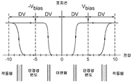
도 3은 도 1의 간섭 변조기에 대한 이동가능 반사층 포지션 대 인가된 전압을 예시하는 다이어그램의 일 예를 도시한다. MEMS 간섭 변조기들에 대해, 행/열 (즉, 공통/세그먼트) 쓰기 프로시저는 도 3에 예시된 바와 같은 이들 디바이스들의 히스테리시스 특성의 이점을 이용할 수도 있다. 간섭 변조기는 이동가능 반사층, 또는 거울로 하여금, 이완된 상태로부터 작동된 상태로 변화하도록, 예를 들어, 약 10-볼트 전위차를 요구할 수도 있다. 전압이 그 값으로부터 감소되는 경우, 전압이, 예컨대, 10-볼트 미만으로 다시 강하함에 따라 이동가능 반사층은 그것의 상태를 유지하지만, 이동가능 반사층은 전압이 2-볼트 미만으로 강하하기까지 완전히 이완되지 않는다. 따라서, 도 3에 도시된 바와 같은 전압의 범위, 대략 3 내지 7-볼트는, 디바이스가 이완된 또는 작동된 상태에서 안정한 범위가 되는 인가된 전압의 윈도가 존재하는 경우에 존재한다. 이는 본원에서는 "히스테리시스 윈도" 또는 "안정성 윈도 (stability window)"라고 지칭된다. 도 3의 히스테리시스 특성들을 갖는 디스플레이 어레이 (30) 의 경우, 행/열 쓰기 프로시저는 하나 이상의 행들을 한 번에 어드레싱하도록 설계될 수 있어서, 주어진 행의 어드레싱 동안, 작동될 어드레싱된 행의 화소들은 약 10-볼트의 전압차에 노출되고, 이완될 화소들은 거의 0 볼트의 전압차에 노출된다. 어드레싱 후, 화소들은 그것들이 이전의 스트로빙 상태로 유지되도록 정상 (steady) 상태 또는 대략 5-볼트의 바이어스 전압차에 노출된다. 이 예에서, 어드레싱된 후, 각각의 화소는 약 3-7 볼트의 "안정성 윈도" 내의 전위차를 보인다. 이 히스테리시스 특성 특징은 동일한 인가된 전압 조건들 하의 작동된 또는 이완된 미리 존재하는 상태를 유지하기 위해, 예컨대, 도 1에 예시된 화소 설계를 가능하게 한다. 각각의 IMOD 화소는, 작동된 상태이든 또는 이완된 상태이든, 근본적으로는 고정된 및 가동 반사층들에 의해 형성된 커패시터이므로, 이 안정한 상태는 전력을 실질적으로 낭비하거나 손실하는 일 없이 히스테리시스 윈도 내의 정상 전압에서 유지될 수 있다. 더구나, 인가된 전압 전위가 실질적으로 고정되게 유지된다면 IMOD 화소 속으로 흐르는 전류는 근본적으로 적거나 또는 없다.3 shows an example of a diagram illustrating movable reflective layer position versus applied voltage for the interference modulator of FIG. 1. For MEMS interference modulators, the row / column (ie common / segment) write procedure may take advantage of the hysteresis characteristics of these devices as illustrated in FIG. 3. The interferometric modulator may require, for example, about 10-volt potential difference to cause the movable reflective layer, or mirror, to change from a relaxed state to an activated state. If the voltage decreases from that value, the movable reflective layer remains intact as the voltage drops back below, eg, 10-volts, but the movable reflective layer is fully relaxed until the voltage drops below 2-volts. It doesn't work. Thus, the range of voltages, approximately 3 to 7-volts, as shown in FIG. 3, is present when there is a window of applied voltages that is in a stable range with the device relaxed or in operation. This is referred to herein as a "hysteresis window" or "stability window." For
일부 구현예들에서, 이미지의 프레임은 주어진 행에서의 화소들의 상태에 대한 소망의 변화에 (만약에 있다면) 따라서, 열 전극들의 세트를 따라 "세그먼트" 전압들의 형태로 데이터 신호들을 인가함으로써 만들어질 수도 있다. 어레이의 각각의 행은 차례로 어드레싱될 수 있어서, 프레임이 한 번에 한 행씩 쓰여진다. 소망의 데이터를 제 1 행의 화소들에 쓰기 위해, 제 1 행에서의 화소들의 소망의 상태에 대응하는 세그먼트 전압들은 열 전극들에 인가될 수 있고, 특정 "공통" 전압 또는 신호의 형태의 제 1 행 펄스는 제 1 행 전극에 인가될 수 있다. 그 다음에 세그먼트 전압들의 세트는 제 2 행의 화소들의 상태에 대한 소망의 변화에 (만약에 있다면) 대응하게 변화될 수 있고, 제 2 공통 전압은 제 2 행 전극에 인가될 수 있다. 일부 구현예들에서, 제 1 행의 화소들은 열 전극들을 따라 인가된 세그먼트 전압들에서의 변화에 의해 영향을 받지 않고, 제 1 공통 전압 행 펄스 동안에 그것들이 설정되었던 상태로 유지된다. 이 프로세스는 이미지 프레임을 생성하기 위해 전체 일련의 행들, 또는 대안으로, 열들에 대해 순차적 형태로 반복될 수도 있다. 그 프레임들은 이 프로세스를 초당 일부 소망의 수의 프레임들로 계속해서 반복함으로써 새로운 이미지 데이터로 리프레시 및/또는 업데이트될 수 있다.In some implementations, a frame of an image can be created by applying data signals in the form of "segment" voltages along a set of column electrodes, according to (if any) a desired change in the state of the pixels in a given row. It may be. Each row of the array can be addressed in turn so that the frame is written one row at a time. In order to write the desired data to the pixels of the first row, the segment voltages corresponding to the desired state of the pixels in the first row can be applied to the column electrodes, and the specific "common" voltage or in the form of a signal One row pulse may be applied to the first row electrode. The set of segment voltages can then be changed (if any) corresponding to the desired change to the state of the pixels in the second row, and the second common voltage can be applied to the second row electrode. In some implementations, the pixels of the first row are not affected by changes in the segment voltages applied along the column electrodes, and remain in the state where they were set during the first common voltage row pulse. This process may be repeated in sequential form over the entire series of rows, or alternatively, columns, to produce an image frame. The frames can be refreshed and / or updated with new image data by repeatedly repeating this process with some desired number of frames per second.
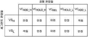
각각의 화소에 걸리게 인가된 세그먼트 및 공통 신호들의 조합 (다시 말하면, 각각의 화소에 걸리는 전위차) 은 각각의 화소의 결과적인 상태를 결정한다. 도 4는 갖가지 공통 및 세그먼트 전압들이 인가되는 경우에 간섭 변조기의 갖가지 상태들을 예시하는 테이블의 일 예를 도시한다. 이 기술분야의 통상의 지식을 가진자에 의해 쉽사리 이해될 바와 같이, "세그먼트" 전압들은 열 전극들 또는 행 전극들 중 어느 하나에 인가될 수 있고, "공통" 전압들은 열 전극들 또는 행 전극들 중 나머지 하나에 인가될 수 있다.The combination of segments and common signals applied across each pixel (ie, the potential difference across each pixel) determines the resulting state of each pixel. 4 shows an example of a table illustrating various states of an interference modulator when various common and segment voltages are applied. As will be readily understood by one of ordinary skill in the art, "segment" voltages can be applied to either column electrodes or row electrodes, and "common" voltages are column electrodes or row electrodes. May be applied to the other of the two.
도 4에서 (뿐만 아니라 도 5b에 도시된 타이밍도에서) 예시된 바와 같이, 릴리스(release) 전압 (VCREL) 이 공통선을 따라 인가되는 경우, 공통선을 따르는 모든 간섭 변조기 엘리먼트들은, 세그먼트선들을 따라 인가된 전압, 즉, 하이 세그먼트 전압 (VSH) 및 로우 세그먼트 전압 (VSL) 에 무관하게, 대안으로는 릴리스된 (released) 또는 작동되지 않은 상태라고 지칭되는 이완된 상태로 배치될 것이다. 특히, 릴리스 전압 (VCREL) 이 공통선을 따라 인가되는 경우, 변조기에 걸리는 포텐셜 전압 (다르게는 화소 전압이라 지칭됨) 은, 하이 세그먼트 전압 (VSH) 및 로우 세그먼트 전압 (VSL) 둘 다가 그 화소에 대한 대응하는 세그먼트선을 따라 인가되는 경우에 이완 윈도 (relaxation window)(도 3 참조, 또한 릴리스 윈도라고 지칭됨) 내에 있다.As illustrated in FIG. 4 (as well as in the timing diagram shown in FIG. 5B), when a release voltage VC REL is applied along a common line, all interference modulator elements along the common line are segment lines. Regardless of the voltage applied along, i.e., the high segment voltage VS H and the low segment voltage VS L , it will alternatively be placed in a relaxed state, referred to as a released or inoperative state. . In particular, when the release voltage VC REL is applied along a common line, the potential voltage across the modulator (also referred to as pixel voltage) is equal to both the high segment voltage VS H and the low segment voltage VS L. It is within a relaxation window (see FIG. 3, also referred to as a release window) when applied along the corresponding segment line for that pixel.
하이 유지 전압 (VCHOLD _H) 또는 로우 유지 전압 (VCHOLD _L) 과 같은 유지 전압이 공통선에 인가되는 경우, 간섭 변조기의 상태는 일정하게 유지될 것이다. 예를 들어, 이완된 IMOD는 이완된 포지션으로 유지될 것이고, 작동된 IMOD는 작동된 포지션으로 유지될 것이다. 하이 세그먼트 전압 (VSH) 및 로우 세그먼트 전압 (VSL) 둘 다가 대응하는 세그먼트선을 따라 인가되는 경우에 화소 전압이 안정성 윈도 내에 유지되도록 유지 전압들은 선택될 수 있다. 따라서, 세그먼트 전압 스윙, 즉, 하이 (VSH) 및 로우 세그먼트 전압 (VSL) 사이의 차이는, 양의 또는 음의 안정성 윈도의 폭 미만이다.If the holding voltage as the high holding voltage (VC HOLD _H) or a low holding voltage (VC HOLD _L) is applied to the common line, the state of the interference modulator will remain constant. For example, a relaxed IMOD will remain in a relaxed position and an activated IMOD will remain in an activated position. The sustain voltages can be selected so that the pixel voltage remains within the stability window when both the high segment voltage VS H and the low segment voltage VS L are applied along the corresponding segment line. Thus, the segment voltage swing, i.e., the difference between the high VS H and the low segment voltage VS L is less than the width of the positive or negative stability window.
어드레싱 또는 작동 전압, 이를테면 하이 어드레싱 전압 (VCADD _H) 또는 로우 어드레싱 (전압 (VCADD _L) 이 공통선에 인가되는 경우, 데이터는 개별 세그먼트선들에 따른 세그먼트 전압들의 인가에 의해 그 공통선을 따라 변조기들에 선택적으로 쓰여질 수 있다. 세그먼트 전압들은 인가된 세그먼트 전압에 작동이 의존하도록 선택될 수도 있다. 어드레싱 전압이 공통선을 따라 인가되는 경우, 하나의 세그먼트 전압의 인가는 결과적으로 화소 전압이 안정성 윈도 내에 있게 하여, 그 화소가 작동하지 않게 유지되게 한다. 그 반면, 다른 세그먼트 전압의 인가는 결과적으로 화소 전압이 안정성 윈도를 벗어나게 하여, 결국 화소의 작동이 되게 한다. 작동을 유발하는 특정 세그먼트 전압은 어떤 어드레싱 전압이 이용되는지에 의존하여 가변할 수 있다. 일부 구현예들에서, 하이 어드레싱 전압 (VCADD_H) 이 공통선을 따라 인가되는 경우, 하이 세그먼트 전압 (VSH) 의 인가는 변조기로 하여금 그것의 현재 포지션으로 유지되게 할 수 있는 반면, 로우 세그먼트 전압 (VSL) 의 인가는 변조기의 작동을 유발할 수 있다. 그 결과, 세그먼트 전압들의 영향은 로우 어드레싱 전압 (VCADD _L) 이 인가되는 경우에 반대로 될 수 있어, 하이 세그먼트 전압 (VSH) 은 변조기의 작동을 유발하고, 로우 세그먼트 전압 (VSL) 은 변조기의 상태에 영향을 주지 않는다 (즉, 안정을 유지한다).If an addressing or operating voltage such as a high addressing voltage VC ADD _H or a low addressing voltage VC ADD _L is applied to the common line, the data is along that common line by application of segment voltages along the individual segment lines. May be selectively written to the modulators Segment voltages may be selected such that the operation depends on the applied segment voltage When the addressing voltage is applied along a common line, the application of one segment voltage results in a stable pixel voltage. To remain within the window, leaving the pixel inoperable, while the application of other segment voltages results in the pixel voltage leaving the stability window, resulting in pixel operation. Can vary depending on which addressing voltage is used. In implementations, when the high addressing voltage VC ADD_H is applied along a common line, the application of the high segment voltage VS H may cause the modulator to remain at its current position, while the low segment voltage ( The application of VS L ) can cause the operation of the modulator, as a result of which the influence of the segment voltages can be reversed when the low addressing voltage VC ADD _ L is applied, so that the high segment voltage VS H Causes operation, the low segment voltage VS L does not affect the state of the modulator (ie, remains stable).
일부 구현예들에서, 변조기들에 걸리는 동일한 극성의 전위차를 항상 생성하는, 유지 전압들, 어드레스 전압들, 및 세그먼트 전압들이 이용될 수도 있다. 일부 다른 구현예들에서, 변조기들의 전위차의 극성을 교호시키는 신호들이 이용될 수 있다. 변조기들에 걸리는 극성의 교호 (다시 말하면, 쓰기 프로시저들의 극성의 교호) 는 단일 극성의 반복된 쓰기 동작들 후에 일어날 수 있는 전하 축적을 줄이거나 또는 억제할 수도 있다.In some implementations, sustain voltages, address voltages, and segment voltages may be used, which always produce a potential difference of the same polarity across the modulators. In some other implementations, signals can be used that alternate the polarity of the potential difference of the modulators. The alternating polarity across the modulators (ie, the alternating polarity of the write procedures) may reduce or suppress charge buildup that may occur after repeated write operations of a single polarity.
도 5a는 도 2의 3x3 간섭 변조기 디스플레이에서의 디스플레이 데이터의 프레임을 예시하는 다이어그램의 일 예를 도시한다. 도 5b는 도 5a에 예시된 디스플레이 데이터의 프레임을 쓰는데 이용될 수도 있는 공통 및 세그먼트 신호들에 대한 타이밍도의 일 예를 도시한다. 그 신호들은, 예컨대, 도 2의 3x3 어레이에 인가될 수 있으며, 이는 궁극적으로 도 5a에 예시된 라인 시간 (60e) 디스플레이 배열이 될 것이다. 도 5a의 작동된 변조기들은 어두운-상태에 있다, 즉, 그 경우 반사된 광의 실질적 부분은, 예컨대, 관람자에게 어두운 외관이 되도록 하기 위해서 가시 스펙트럼의 바깥쪽에 있다. 도 5a에 예시된 프레임을 쓰기 전에, 화소들은 임의의 상태에 있을 수 있지만, 도 5b의 타이밍도에 예시된 쓰기 프로시저는 각각의 변조기가 릴리스되었고 제 1 라인 시간 (60a) 전에 작동되지 않은 상태로 존재한다고 상정한다.FIG. 5A shows an example of a diagram illustrating a frame of display data in the 3x3 interferometric modulator display of FIG. 2. FIG. 5B shows an example of a timing diagram for common and segment signals that may be used to write the frame of display data illustrated in FIG. 5A. The signals can be applied, for example, to the 3x3 array of FIG. 2, which will ultimately be the
제 1 라인 시간 (60a) 동안, 릴리스 전압 (70) 이 공통선 1에 인가되며; 공통선 2에 인가된 전압은 하이 유지 전압 (72) 에서 시작하고 릴리스 전압 (70) 으로 이동하며; 그리고 로우 유지 전압 (76) 은 공통선 3을 따라 인가된다. 따라서, 공통선 1을 따르는 변조기들인 (공통 1, 세그먼트 1), (1,2) 및 (1,3) 은 제 1 라인 시간 (60a) 의 지속시간 동안 이완된, 또는 작동하지 않은 상태로 유지되며, 공통선 2를 따르는 변조기들인 (2,1), (2,2) 및 (2,3) 은 이완된 상태로 이동할 것이고, 공통선 3을 따르는 변조기들인 (3,1), (3,2) 및 (3,3) 은 그것들의 이전의 상태로 유지될 것이다. 도 4를 참조하면, 세그먼트선들 (1, 2 및 3) 을 따라 인가된 세그먼트 전압들은, 공통선들 (1, 2 또는 3) 중의 어느 것도 라인 시간 (60a) 동안 작동을 유발할 전압 레벨들에 노출되어 있지 않을 것 (즉, VCREL - 이완 및 VCHOLD _L - 안정) 이므로, 간섭 변조기들의 상태에 영향을 주지 않을 것이다.During the
제 2 라인 시간 (60b) 동안, 공통선 1 상의 전압은 하이 유지 전압 (72) 으로 이동하고, 공통선 1을 따르는 모든 변조기들은 인가된 세그먼트 전압에 무관하게 이완된 상태로 유지되는데, 어드레싱 또는 작동 전압이 공통선 1에 인가되지 않았기 때문이다. 공통선 2를 따르는 변조기들은 릴리스 전압 (70) 의 인가로 인해 이완된 상태로 유지되고, 공통선 3을 따르는 변조기들인 (3,1), (3,2) 및 (3,3) 은 공통선 3을 따르는 전압이 릴리스 전압 (70) 으로 이동하는 경우에 이완될 것이다.During the second line time 60b, the voltage on
제 3 라인 시간 (60c) 동안, 공통선 1은 하이 어드레스 전압 (74) 을 공통선 1에 인가함으로써 어드레싱된다. 이 어드레스 전압의 인가 동안에 로우 세그먼트 전압 (64) 이 세그먼트선들 (1 및 2) 을 따라 인가되기 때문에, 변조기들인 (1,1) 및 (1,2) 에 걸리는 화소 전압은 변조기들의 양의 안정성 윈도의 상한(high end)보다 크고 (즉, 전압차가 미리 정의된 임계치를 초과하였음), 변조기들인 (1,1) 및 (1,2) 는 작동된다. 반대로, 하이 세그먼트 전압 (62) 이 세그먼트선 3을 따라 인가되기 때문에, 변조기 (1,3) 에 걸리는 화소 전압은 변조기들인 (1,1) 및 (1,2) 의 화소 전압 미만이고, 변조기의 양의 안정성 윈도 내에 유지되며, 변조기 (1,3) 은 따라서 이완된 채로 유지된다. 또한 라인 시간 (60c) 동안, 공통선 2를 따르는 전압은 로우 유지 전압 (76) 으로 감소하고, 공통선 3을 따르는 전압은 릴리스 전압 (70) 으로 유지되어, 공통선들 (2 및 3) 을 따르는 변조기들을 이완된 포지션으로 남겨둔다.During the
제 4 라인 시간 (60d) 동안, 공통선 1 상의 전압은 하이 유지 전압 (72) 으로 복귀하여, 공통선 1을 따르는 변조기들은 그것들의 개별 어드레싱된 상태들로 남겨둔다. 공통선 2 상의 전압은 로우 어드레스 전압 (78) 으로 감소된다. 하이 세그먼트 전압 (62) 이 세그먼트선 2를 따라 인가되기 때문에, 변조기 (2,2) 에 걸리는 화소 전압은 변조기의 음의 안정성 윈도의 하한(lower end) 미만이 되어, 변조기 (2,2) 가 작동되게 한다. 반대로, 로우 세그먼트 전압 (64) 이 세그먼트선들 (1 및 3) 에 인가되기 때문에, 변조기들인 (2,1) 및 (2,3) 은 이완된 포지션으로 유지된다. 공통선 3 상의 전압은 하이 유지 전압 (72) 으로 증가하여, 공통선 3을 따르는 변조기들을 이완된 상태로 남겨둔다. 그 다음에 공통선 2 상의 전압은 로우 유지 전압 (76) 으로 다시 전이된다.During the
마지막으로, 제 5 라인 시간 (60e) 동안, 공통선 1 상의 전압은 하이 유지 전압 (72) 으로 유지되고, 공통선 2 상의 전압은 로우 유지 전압 (76) 으로 유지되어, 공통선들 (1 및 2) 을 따르는 변조기들을 그것들의 개별 어드레싱된 상태들로 남겨둔다. 공통선 3 상의 전압은 공통선 3을 따르는 변조기들을 어드레싱하기 위해 하이 어드레스 전압 (74) 으로 증가한다. 로우 세그먼트 전압 (64) 이 세그먼트선들 (2 및 3) 에 인가됨에 따라, 변조기들인 (3,2) 및 (3,3) 은 작동하는 반면, 세그먼트선 1을 따라 인가된 하이 세그먼트 전압 (62) 은 변조기 (3,1) 이 이완된 포지션으로 유지되게 한다. 따라서, 제 5 라인 시간 (60e) 의 끝에서, 3x3 화소 어레이는 도 5a에 도시된 상태에 있고, 다른 공통선들 (미도시) 을 따르는 변조기들이 어드레싱 중인 경우에 발생할 수도 있는 세그먼트 전압에서의 변동들에 무관하게, 유지 전압들이 공통선들을 따라 인가되는 한, 그 상태로 유지될 것이다.Finally, during the
도 5b의 타이밍도에서, 주어진 쓰기 프로시저 (즉, 라인 시간들 (60a-60e)) 는 하이 유지 및 어드레스 전압들, 또는 로우 유지 및 어드레스 전압들의 사용을 포함할 수 있다. 일단 쓰기 프로시저가 주어진 공통선에 대해 완료되면 (그리고 공통 전압이 작동 전압과 동일한 극성을 갖는 유지 전압으로 설정되면), 화소 전압은 주어진 안정성 윈도 내에 유지되고, 릴리스 전압이 그 공통선에 인가되기까지 이완 윈도를 통과하지 않는다. 더욱이, 각각의 변조기가 변조기를 어드레싱하기 전에 쓰기 프로시저의 부분으로서 릴리스되므로, 릴리스 시간보다는, 변조기의 작동 시간이, 필요한 라인 시간을 결정할 수도 있다. 구체적으로는, 변조기의 릴리스 작동 시간보다 큰 구현예들에서, 릴리스 전압은, 도 5b에 묘사된 바와 같이, 단일 라인 시간보다 더 길게 인가될 수도 있다. 일부 다른 구현예들에서, 공통선들 또는 세그먼트선들을 따라 인가된 전압들은 다른 변조기들, 이를테면 상이한 컬러들의 변조기들의 작동 및 릴리스 전압들에서의 변동들에 대응하기 위해 가변할 수도 있다.In the timing diagram of FIG. 5B, a given write procedure (ie,
위에서 언급된 원리들에 따라서 동작하는 간섭 변조기들의 구조의 세부사항들은 광범위하게 달라질 수도 있다. 예를 들어, 도 6a-6e는 이동가능 반사층 (14) 및 그것의 지지 구조들을 구비한, 간섭 변조기들의 변화하는 구현예들의 단면들의 예들을 도시한다. 도 6a는 도 1의 간섭 변조기 디스플레이의 부분 단면의 일 예를 도시하며, 여기서 금속 재료의 스트립, 즉, 이동가능 반사층 (14) 은 기판 (20) 으로부터 직교하게 연장하는 지지물들 (18) 상에 퇴적된다. 도 6b에서, 각각의 IMOD의 이동가능 반사층 (14) 은 일반적으로 형상이 정사각형 또는 직사각형이고 테더들 (tethers) (32) 상의 코너들에서 또는 그 코너들 가까이에서 지지물들에 부착된다. 도 6c에서, 이동가능 반사층 (14) 은 일반적으로 형상이 정사각형 또는 직사각형이고 유연한 금속을 포함할 수도 있는 변형가능 층 (34) 에 메달려 있다. 변형가능 층 (34) 은 이동가능 반사층 (14) 의 주위를 둘러싸게 기판 (20) 에 직접적으로 또는 간접적으로 연결될 수 있다. 이런 연결체들은 본원에서는 지지 포스트들이라 지칭된다. 도 6c에 도시된 구현예는 이동가능 반사층 (14) 의 광학적 기능들의, 변형가능 층 (34) 에 의해 행해지는 그것의 기계적 기능들로부터의 분리로 도출되는 부가적인 이점들을 가진다. 이 분리는 반사층 (14) 을 위해 사용된 구조적 설계 및 재료들과 변형가능 층 (34) 을 위해 사용된 구조적 설계 및 재료들이 서로 독립적으로 최적화되는 것을 허용한다.The details of the structure of the interferometric modulators operating in accordance with the principles mentioned above may vary widely. For example, FIGS. 6A-6E show examples of cross sections of varying implementations of interferometric modulators, with movable
도 6d는 이동가능 반사층 (14) 이 반사 서브층 (14a) 을 포함하는 IMOD의 다른 예를 도시한다. 이동가능 반사층 (14) 은 지지 구조, 이를테면 지지 포스트들 (18) 상에 놓여있다. 지지 포스트들 (18) 은 하부 정지 전극 (즉, 예시된 IMOD에서의 광학적 스택 (16) 의 부분) 으로부터 이동가능 반사층 (14) 의 분리를 제공하여서, 예를 들어 이동가능 반사층 (14) 이 이완된 포지션에 있는 경우에 갭 (19) 이 이동가능 반사층 (14) 및 광학적 스택 (16) 사이에 형성된다. 이동가능 반사층 (14) 은 또한 전극으로서 역할을 하도록 구성될 수도 있는 도전층 (14c), 및 지지 층 (14b) 을 구비할 수 있다. 이 예에서, 도전층 (14c) 은 기판 (20) 으로부터 먼쪽의, 지지 층 (14b) 의 일 측에 배치되고, 반사 서브층 (14a) 은 기판 (20) 에 가까운 쪽의, 지지 층 (14b) 의 타 측에 배치된다. 일부 구현예들에서, 반사 서브층 (14a) 은 도전성일 수 있고 지지 층 (14b) 및 광학적 스택 (16) 사이에 배치될 수 있다. 지지 층 (14b) 은 유전체 재료, 예를 들어, 실리콘 산화질화물 (SiON) 또는 실리콘 이산화물 (SiO2) 의 하나 이상의 층들을 포함할 수 있다. 일부 구현예들에서, 지지 층 (14b) 은, 예를 들어, SiO2/SiON/SiO2 삼-층 스택과 같은 층들의 스택일 수 있다. 반사 서브층 (14a) 및 도전층 (14c) 의 어느 하나 또는 양쪽 모두는, 예컨대, 약 0.5% 구리 (Cu) 를 갖는 알루미늄 (Al) 합금, 또는 다른 반사성 금속 재료를 포함할 수 있다. 유전체 지지 층 (14b) 위쪽 및 아래쪽에 도전층들 (14a, 14c) 을 채용하는 것은 응력들 (stresses) 의 균형을 잡을 수 있고 향상된 도전율 (conduction) 을 제공할 수 있다. 일부 구현예들에서, 반사 서브층 (14a) 및 도전층 (14c) 은 다양한 설계 목적들을 위해, 이를테면 이동가능 반사층 (14) 내에서 특정 응력 프로파일들을 달성하기 위해 상이한 재료들로 형성될 수 있다.6D shows another example of an IMOD where the movable
도 6d에 예시된 바와 같이, 일부 구현예들은 또한 흑색 마스크 구조 (23) 를 구비할 수 있다. 흑색 마스크 구조 (23) 는 광학적으로 비활성 지역들 내에 (예컨대, 화소들 사이에 또는 포스트들 (18) 아래에) 주변광 또는 미광 (stray light) 을 흡수하기 위해 형성될 수 있다. 흑색 마스크 구조 (23) 는 또한 광이 디스플레이의 비활성 부분들에서 반사되거나 또는 그 부분들을 투과하는 것을 억제하며, 이에 의해 콘트라스트 비를 증가시킴으로써, 디스플레이 디바이스의 광학적 특성들을 개선할 수 있다. 덧붙여, 흑색 마스크 구조 (23) 는 도전성일 수 있고 전기 부싱 층으로서 기능을 하도록 구성될 수 있다. 일부 구현예들에서, 행 전극들은 접속된 행 전극의 저항을 줄이기 위해 흑색 마스크 구조 (23) 에 접속될 수 있다. 흑색 마스크 구조 (23) 는 퇴적 및 패터닝 기법들을 포함한, 다양한 방법들을 이용하여 형성될 수 있다. 흑색 마스크 구조 (23) 는 하나 이상의 층들을 구비할 수 있다. 예를 들어, 일부 구현예들에서, 흑색 마스크 구조 (23) 는 각각 약 30 - 80 Å, 500 - 1000 Å, 및 500 - 6000 Å의 범위의 두께를 가지는, 광학적 흡수체로서 역할을 하는 몰리브덴-크롬 (MoCr) 층, SiO2 층, 및 반사체 및 부싱 층으로서 역할을 하는 알루미늄 합금을 포함한다. 하나 이상의 층들은, 예를 들어, MoCr 및 SiO2 층들에 대한 탄소 테트라플루오로메탄 (CF4) 및/또는 산소 (O2) 와 알루미늄 합금 층에 대한 염소 (Cl2) 및/또는 붕소 3염화물 (BCl3) 을 포함하는, 건식 에칭 및 포토리소그래피를 포함하는 다양한 기법들을 이용하여 패턴화될 수 있다. 일부 구현예들에서, 흑색 마스크 (23) 는 에탈론 (etalon) 또는 간섭 스택 구조일 수 있다. 이러한 간섭형 스택 흑색 마스크 구조들 (23) 에서, 도전성 흡수체들은 각각의 행 또는 열의 광학적 스택 (16) 에서의 하부, 정지 전극들 간에 신호들을 전달 또는 버스전달 (bus) 하는데 사용될 수 있다. 일부 구현예들에서, 스페이서 층 (35) 은 일반적으로 흡수체 층 (16a) 을 흑색 마스크 (23) 에서의 도전층들로부터 전기적으로 절연시키는 역할을 할 수 있다.As illustrated in FIG. 6D, some embodiments may also have a
도 6e는 이동가능 반사층 (14) 이 자체 지지형인 IMOD의 다른 예를 도시한다. 도 6d와 대조적으로, 도 6e의 구현예는 지지 포스트들 (18) 을 구비하지 않는다. 대신에, 이동가능 반사층 (14) 은 밑에 있는 광학적 스택 (16) 과 다수의 로케이션들에서 접촉하고, 이동가능 반사층 (14) 의 곡률은 간섭 변조기에 걸리는 전압이 작동을 유발하는데 충분하지 않은 경우에 이동가능 반사층 (14) 이 도 6e의 작동되지 않은 포지션으로 복귀하는 것을 충분히 지지한다. 복수의 여러 상이한 층들을 포함할 수도 있는 광학적 스택 (16) 은, 여기서 명료함을 위해 광학적 흡수체 (16a), 및 유전체 (16b) 를 포함하는 것으로 도시된다. 일부 구현예들에서, 광학적 흡수체 (16a) 는 고정된 전극으로서 뿐만 아니라 부분 반사층으로서도 역할을 할 수도 있다.6E shows another example of an IMOD where the movable
도 6a-6e에 도시된 것들과 같은 구현예들에서, IMOD들은 이미지들이 투명 기판 (20) 의 앞면, 즉, 변조기가 배열된 쪽과 반대인 쪽에서 보이는 직접 뷰 디바이스들로서 기능을 한다. 이들 구현예들에서, 디바이스의 뒷면 부분들 (다시 말하면, 예를 들어, 도 6c에 예시된 변형가능 층 (34) 을 포함하여, 이동가능 반사층 (14) 뒤의 디스플레이 디바이스의 임의의 부분) 은 디스플레이 디바이스의 이미지 품질에 강한 영향 또는 악영향을 주는 일 없이 구성되고 동작될 수 있는데, 반사층 (14) 이 디바이스의 그 부분들을 광학적으로 차폐하기 때문이다. 예를 들어, 일부 구현예들에서 버스 구조 (예시되지 않음) 는 변조기의 광학적 특성들을 변조기의 전기기계적 특성들, 이를테면 전압 어드레싱 및 이러한 어드레싱으로부터 생겨나는 이동들로부터 분리하는 능력을 제공하는 이동가능 반사층 (14) 뒤에 구비될 수 있다. 덧붙여, 도 6a-6e의 구현예들은 프로세싱, 이를테면 패턴화를 단순화시킬 수 있다.In implementations such as those shown in FIGS. 6A-6E, the IMODs function as direct viewing devices where the images are seen on the front side of the
도 7은 간섭 변조기에 대한 제조 프로세스 (80) 를 예시하는 흐름도의 일 예를 도시하고, 도 8a-8e는 간섭 변조기를 만드는 방법에서의 여러 스테이지들의 단면 개략도들의 예들을 도시한다. 일부 구현예들에서, 제조 프로세스 (80) 는 도 7에 도시되지 않은 다른 블록들 외에도, 예컨대, 도 1 및 6에 예시된 일반 유형의 간섭 변조기들을 제조하기 위해 구현될 수 있다. 도 1, 6 및 7을 참조하면, 프로세스 (80) 는 블록 82에서 기판 (20) 상의 광학적 스택 (16) 의 형성으로 개시된다. 도 8a는 기판 (20) 상에 형성된 이러한 광학적 스택 (16) 을 예시한다. 기판 (20) 은 유리 또는 플라스틱과 같은 투명 기판일 수도 있으며, 그것은 유연한 또는 비교적 딱딱하고 휘지 않을 수도 있고, 광학적 스택 (16) 의 효율적인 형성을 용이하게 하기 위해 사전 준비 프로세스들, 예컨대, 세정을 받았을 수도 있다. 위에서 논의된 바와 같이, 광학적 스택 (16) 은 도전성이며, 부분적으로 투과성이고 부분적으로 반사성이며, 그리고, 예를 들어, 소망의 특성들을 갖는 하나 이상의 층들을 투명 기판 (20) 상에 퇴적함으로써 제작될 수도 있다. 도 8a에서, 광학적 스택 (16) 은 서브층들 (16a 및 16b) 을 갖는 다층 구조를 포함하지만, 더 많거나 더 적은 서브층들이 일부 다른 구현예들에서 포함될 수도 있다. 일부 구현예들에서, 서브층들 (16a, 16b) 중 하나는 광학적 흡수성 및 도전성 특성들 양쪽 모두를 갖게 구성될 수 있다, 이를테면 결합형 도전체/흡수체 서브층 (16a) 일 수 있다. 덧붙여, 서브층들 (16a, 16b) 중 하나 이상은 평행한 스트립들로 패턴화될 수 있고, 디스플레이 디바이스에 행 전극들을 형성할 수도 있다. 이러한 패턴화는 마스킹 및 에칭 공정 또는 이 기술분야에서 알려진 다른 적합한 프로세스에 의해 형성될 수 있다. 일부 구현예들에서, 서브층들 (16a, 16b) 중 하나는 절연성 또는 유전체 층, 이를테면 하나 이상의 금속 층들 (예컨대, 하나 이상의 반사 및/또는 도전층들) 상에 퇴적되는 서브층 (16b) 일 수 있다. 덧붙여서, 광학적 스택 (16) 은 디스플레이의 행들을 형성하는 개개의 및 평행한 스트립들로 패턴화될 수 있다.7 shows an example of a flow diagram illustrating a
프로세스 (80) 는 블록 84에서 광학적 스택 (16) 상의 희생층 (25) 의 형성과 함께 계속된다. 희생층 (25) 은 공동 (19) 을 형성하기 위해 나중에 (예컨대, 블록 90에서) 제거되고 이에 따라 희생층 (25) 은 도 1에 예시된 결과적인 간섭 변조기들 (12) 에서 보여지지 않는다. 도 8b는 광학적 스택 (16) 상에 형성된 희생층 (25) 을 포함하는 부분적으로 제작된 디바이스를 예시한다. 광학적 스택 (16) 상의 희생층 (25) 의 형성은, 후속하는 제거 후에, 소망의 설계 사이즈를 갖는 갭 또는 공동 (19) (또한 도 1 및 8e 참조) 을 제공하기 위해 선택된 두께의, 몰리브덴 (Mo) 또는 비정질 실리콘 (Si) 과 같은 크세논 이불화물 (XeF2) 식각가능 재료의 퇴적을 포함할 수도 있다. 희생 재료의 퇴적은 물리적 기상 증착 (PVD, 예컨대, 스퍼터링), 플라즈마 강화 화학 기상 증착 (PECVD), 열 화학 기상 증착 (열 CVD), 또는 스핀 코팅과 같은 퇴적 기법들을 이용하여 수행될 수도 있다.
프로세스 (80) 는 블록 86에서 지지 구조 예컨대, 도 1, 6 및 8c에 예시된 바와 같은 포스트 (18) 의 형성과 함께 계속된다. 포스트 (18) 의 형성은 지지 구조 개구부를 형성하기 위해 희생층 (25) 을 패턴화하는 것, 그 다음에 PVD, PECVD, 열 CVD, 또는 스핀 코팅과 같은 퇴적 방법을 이용하여, 포스트 (18) 를 형성하기 위해 재료 (예컨대, 폴리머 또는 무기질 재료, 예컨대, 실리콘 산화물) 를 개구부 속에 퇴적하는 것을 포함할 수도 있다. 일부 구현예들에서, 희생층 내에 형성된 지지 구조 개구부는 희생층 (25) 및 광학적 스택 (16) 둘 다를 통해, 밑에 있는 기판 (20) 까지 연장할 수 있어서, 포스트 (18) 의 하부 말단은 도 6a에 예시된 바와 같이 기판 (20) 과 접촉한다. 대안으로, 도 8c에 묘사된 바와 같이, 희생층 (25) 내에 형성된 개구부는 희생층 (25) 을 통해 연장할 수 있지만, 광학적 스택 (16) 을 통해 연장할 수 없다. 예를 들어, 도 8e는 광학적 스택 (16) 의 상부 표면과 접촉하는 지지 포스트들 (18) 의 하부 말단들을 예시한다. 포스트 (18), 또는 다른 지지 구조들은, 지지 구조 재료의 층을 희생층 (25) 상에 퇴적하고 희생층 (25) 에서 개구부들로부터 떨어져 위치된 지지 구조 재료의 부분들을 패턴화함으로써 형성될 수도 있다. 지지 구조들은, 도 8c에 예시된 바와 같이 개구부들 내에 위치될 수도 있지만, 또한, 적어도 부분적으로 희생층 (25) 의 일 부분 위로 연장할 수 있다. 위에서 지적했듯이, 희생층 (25) 및/또는 지지 포스트들 (18) 의 패턴화는 패턴화 및 에칭 공정에 의해 수행될 수 있지만, 또한 대안적 에칭 방법들에 의해 수행될 수도 있다.
프로세스 (80) 는 블록 88에서 도 1, 6 및 8d에 예시된 이동가능 반사층 (14) 과 같은 이동가능 반사층 또는 멤브레인의 형성과 함께 계속된다. 이동가능 반사층 (14) 은 하나 이상의 퇴적 단계들, 예컨대, 하나 이상의 패턴화, 마스킹, 및/또는 에칭 단계들과 함께 하나 이상의 퇴적 단계들, 예컨대, 반사층 (예컨대, 알루미늄, 알루미늄 합금) 퇴적을 채용함으로써 형성될 수도 있다. 이동가능 반사층 (14) 은 도전성일 수 있고, 도전층이라고 지칭될 수 있다. 일부 구현예들에서, 이동가능 반사층 (14) 은 도 8d에 도시된 바와 같은 복수의 서브층들 (14a, 14b, 14c) 을 구비할 수도 있다. 일부 구현예들에서, 서브층들, 이를테면 서브층들 (14a, 14c) 중의 하나 이상은, 그것들의 광학적 특성들 때문에 선택된 고반사성 서브층들을 구비할 수도 있고, 다른 서브층 (14b) 은 그것의 기계적 특성들 때문에 선택된 기계적 서브층을 구비할 수도 있다. 희생층 (25) 이 블록 88에서 형성된 부분적으로 제작된 간섭 변조기에 여전히 존재하므로, 이동가능 반사층 (14) 은 이 스테이지에서 통상 이동가능하지 않다. 희생층 (25) 을 포함하는 부분적으로 제작된 IMOD는 또한 본원에서는 "릴리스되지 않은 (unreleased)" IMOD라고 지칭될 수도 있다. 도 1에 관하여 위에서 설명된 바와 같이, 이동가능 반사층 (14) 은 디스플레이의 열들을 형성하는 개개의 및 평행한 스트립들로 패턴화될 수 있다.
프로세스 (80) 는 블록 90에서 공동, 예컨대, 도 1, 6 및 8e에 예시된 바와 같은 공동 (19) 의 형성과 함께 계속된다. 공동 (19) 은 (블록 84에서 퇴적된) 희생 재료 (25) 를 식각제에 노출시킴으로써 형성될 수도 있다. 예를 들어, Mo 또는 비정질 Si와 같은 식각가능 희생 재료는, 소망의 양의 재료를 제거하는데 효과적인 기간 동안, 건식 화학적 에칭에 의해, 예컨대, 희생층 (25) 을 기체 또는 기상 식각제, 이를테면 고체 XeF2로부터 파생된 증기들에 노출시킴으로써 제거될 수도 있는데, 통상 공동 (19) 을 둘러싸는 구조들에 대해 선택적으로 제거된다. 다른 에칭 방법들, 예컨대 습식 에칭 및/또는 플라즈마 에칭 또한 이용될 수도 있다. 희생층 (25) 이 블록 90 동안에 제거되므로, 이동가능 반사층 (14) 은 이 스테이지 후에 통상 이동가능하다. 희생 재료 (25) 의 제거 후, 결과적인 완전히 또는 부분적으로 제작된 IMOD는 본원에서는 "릴리스된(released)" IMOD라고 지칭될 수도 있다.
본원에서 설명되는 일부 구현예들에서, 결합형 센서 디바이스의 적어도 일부는 디스플레이 상에 오버레이될 수 있거나 또는 그렇지 않으면 그 디스플레이와 결합될 수 있는 덮개 유리 장치에 통합될 수도 있다. 덮개 유리 장치는 2, 3 이상의 층들을 가질 수도 있다. 일부 구현예들에서, 덮개 유리 장치는 실질적으로 투명한 및 유연한 상부 기판과 실질적으로 투명한 및 상대적으로 더 단단한 하부 기판을 구비할 수도 있다. 덮개 유리는 기판들 상에 및/또는 사이에 배치된 중간 층들, 이를테면 전극들, 실질적으로 투명한 탄성중합체 층 및/또는 힘 감응 저항기 재료를 포함할 수도 있다. 일부 이런 구현예들에서, 덮개 유리 장치의 하부 기판은 디스플레이 기판 상에 오버레이될 수도 있다.In some implementations described herein, at least a portion of the coupled sensor device may be integrated into a lid glass apparatus that may be overlaid on or otherwise coupled with the display. The lid glass apparatus may have two, three or more layers. In some implementations, the lid glass apparatus may have a substantially transparent and relatively upper substrate and a substantially transparent and relatively harder substrate. The cover glass may include intermediate layers disposed on and / or between the substrates, such as electrodes, a substantially transparent elastomer layer, and / or a force sensitive resistor material. In some such implementations, the bottom substrate of the lid glass apparatus may be overlaid on the display substrate.
도 9a는 덮개 유리 장치의 기판들 상에 형성된 센서 전극들의 일 예를 도시한다. 도 9a에 도시된 예에서, 마름모꼴 형상 실질적 투명 전극들의 3 개의 행들 (915) 은 실질적으로 투명한 상부 기판 (905) 상에서 묘사되고 실질적으로 투명한 마름모꼴 전극들의 7개 열들 (920) 은 실질적으로 투명한 하부 기판 (910) 상에 위치된다. 비교적 적은 행들 및 열들은 여기서 예시의 목적을 위해 도시되지만, 실제 센서 디바이스들에서 행들 및 열들의 수는 수십에서 수백 또는 천 이상까지도 확장될 수도 있다. 행들 및 열들이 대체로 교환가능하고, 여기서는 제한이 의도되지 않음에 주의할 수도 있다. 일부 구현예들에서, 결합형 센서 디바이스 (900) 의 상부 기판 (905) 은 비교적 유연한 재료, 이를테면 유연한 폴리머로 형성될 수도 있다. 일부 이러한 예들에서, 상부 기판 (905) 은 폴리에틸렌 테레프탈레이트 (PET), 폴리에틸렌 나프탈레이트 (PEN), 폴리이미드, 또는 유사한 재료로 만들어진 투명한 (clear) 플라스틱 필름일 수도 있다. 일부 구현예들에서, 상부 기판 (905) 은 0.5 - 5 Gpa의 범위의 탄성 계수를 가질 수도 있다. 하부 기판 (910) 은 유리, 플라스틱, 폴리머 등으로 형성될 수도 있다. 일부 구현예들에서, 하부 기판 (910) 은 디스플레이 기판일 수도 있다. 예를 들어, 일부 구현예들에서 하부 기판 (910) 은 위에서 설명된 투명 기판 (20) 과 동일한 기판일 수도 있다.9A shows an example of sensor electrodes formed on substrates of a lid glass apparatus. In the example shown in FIG. 9A, three
이 예에서, 모든 다른 열 전극 (920) 은 중첩 지역들 (925a) 에서 행 전극들 (915) 의 대응하는 마름모꼴들 하에 직접 위치되는 마름모꼴 전극들을 구비한다. 일부 구현예들은 행 전극들 (915) 및 열 전극들 (920) 의 마름모꼴들의 오프셋들을 가지며, 이로 인해 행 전극들 (915) 및 열 전극들 (920) 에서의 마름모꼴들은 부분적으로 서로 중첩된다.In this example, all
일부 구현예들에서, 행 전극들 (915) 및/또는 열 전극들 (920) 은 정사각형들, 직사각형들, 삼각형들, 원들, 타원들 등과 같은 다른 형상들, 및 프레임, 링, 또는 일련의 접속된 라인 세그먼트들과 같은 형상의 중심에서 대개 개방 지역들을 포함하는 형상들로 형성될 수도 있다. 일부 이러한 형상들의 설명은 2010년 12월 21일자로 출원된 발명 명칭이 "Capacitive Touch Sensing Devices and Methods of Manufacturing Thereof"인 계류중인 미국 특허출원 제12/957,025호의 여러 부분들 (예컨대, 도 11a-11j 및 대응하는 설명) 에 포함되어 있으며 그 내용들은 이로써 그 전체가 참조로 통합된다. 더구나, 대안적 구현예들에서 행 전극들 (915) 은 하부 기판 (910) 상에 형성될 수도 있고 열 전극들 (920) 은 상부 기판 (905) 상에 형성될 수도 있다. 일부 구현예들에서, 행 전극들 (915) 및 열 전극들 (920) 사이에 위치된 압축가능 재료 (1025) 를 포함한 도 10c 및 10d를 참조하여 아래에서 설명되는 바와 같이, 가벼운 터치 (또한 투영 정전용량식 터치 (PCT) 라고 지칭됨) 는 인접한 마름모꼴들 사이의 상호 컨패시턴스에서의 변화를 측정함으로써 검출될 수도 있다. 이런 구현예들에서, 스타일러스와의 접촉은 상부 기판 (905) 이 눌러지는 경우에 행 전극들 (915) 및 열 전극들 (920) 사이의 커패시턴스에서의 변화를 측정함으로써 검출될 수도 있다.In some implementations, the
패턴화된 유전체 재료를 행 전극들 (915) 및 열 전극들 (920) 사이에 갖는 구현예들에서, 대응하는 행 전극들 (915) 및 열 전극들 (920) 사이에 갭들이 형성될 수도 있다. 이런 구현예들에서, 가벼운 터치들은 인접한 전극들 사이의 PCT 측정들을 통해 검출될 수 있고, 스타일러스 눌림들은, 행 전극들 (915) 및 열 전극들 (920) (도 10b 참조) 사이의 유효 평행 판 커패시턴스에서의 변화에 의해 또는 행 전극들 (915) 및 열 전극들 (920) 이 직접 기계적 및 전기적 접촉을 하게 되는 경우 (도 10a 참조) 에 발생하는 저항에서의 변화들을 측정함으로써, 또는 손가락, 스타일러스 선단, 손가락의 융선들 등으로 눌러진 경우 (도 10d 참조) 에 행 전극들 (915) 및 열 전극들 (920) 사이에 위치된 힘 감응 저항기에서의 변화들을 측정함으로써 검출될 수 있다. 힘 감응 저항기들은 필기 및 터치 센서 구역 (1005) 에서, 지문 센서 구역 (1010) 에서, 또는 양쪽 모두에서 행 전극들 (915) 및 열 전극들 (920) 사이에 포함될 수도 있다. 일부 이런 구현예들에서, 스타일러스의 로케이션의 감지 동안의 기생 신호들의 영향을 최소화하기 위해 고저항률층이 행 전극들 (915) 또는 열 전극들 (920) 상에 형성될 수도 있다.In embodiments having a patterned dielectric material between the
도 9b는 덮개 유리 상에 형성된 센서 전극들의 대안적인 예를 도시한다. 도 9b에 도시된 예에서, 행 전극들 (915) 의 마름모꼴들 아래쪽에 마름모꼴들이 놓이는 열 전극들 (920) 은 디자인으로부터 제거되어 있다. 결합형 센서 디바이스 (900) 의 오믹 (ohmc) 멤브레인 스위치들, 저항식 멤브레인 스위치들, 힘 감응 저항성 (FSR) 재료를 갖는 저항식 스위치들, 고정된 직렬 저항기를 갖는 FSR 스위치들, 또는 정전용량식 멤브레인들은, 스타일러스 접촉 및, 일부 경우들에서는, 손가락의 손가락끝 또는 융선들을 검출하기 위해, (중첩 지역들 (925b) 내의) 행 전극들 (915) 및 열 전극들 (920) 사이의 교차부들에 형성될 수도 있다. 이런 구현예들은 외부 프로세싱 회로에 접속될 필요가 있는 열 전극들 (920) 의 수 (도 9b에서의 열 전극들 (920) 및 연관된 커넥션 패드들의 수는 도 9a에서의 열 전극들 (920) 및 커넥션 패드들의 수보다 적음에 주의한다) 를 감소시킬 수 있는데, 동일한 열들이 PCT 방법을 통해 가벼운 터치를 검출하거나 또는 커패시턴스 변화 방법 또는 저항 변화 방법을 통해 스타일러스 접촉을 검출할 목적에 기여하기 때문이다.9B shows an alternative example of sensor electrodes formed on the cover glass. In the example shown in FIG. 9B, the
예를 들어, 터치 모드에서, 매우 가벼운 힘만이 터치를 등록하는데 필요할 수도 있다. 그러나, 필기 모드에서, 센서는, 포인팅 디바이스가 도전성인지 또는 비도전성인지에 무관하게, 스타일러스, 펜, 또는 다른 포인터 입력의 많은 형태들을 수용하도록 구성될 수도 있다. 본원에서 설명되는 일부 구현예들은, 지문 센서 모드로 동작 중인 동안 지문을 읽는 경우에 일어날 수도 있는, 다수의 다중-터치 이벤트들을 동시에 구별하거나, 또는 필기 센서 모드로 동작중인 경우에 우연한 손바닥 터치를 검출하고 거부할 수 있는 센서들을 제공한다.For example, in touch mode, only very light forces may be needed to register a touch. However, in the handwriting mode, the sensor may be configured to accept many forms of stylus, pen, or other pointer input, regardless of whether the pointing device is conductive or non-conductive. Some implementations described herein simultaneously distinguish multiple multi-touch events, which may occur when reading a fingerprint while operating in fingerprint sensor mode, or detect accidental palm touch when operating in handwriting sensor mode. And sensors that can be rejected.
도 10a는 결합형 센서 디바이스의 단면도의 일 예를 도시한다. 도 10a에 도시된 센서 어레이는 결합식 터치, 스타일러스, 및 지문 센서로서 묘사되지만, 도 10a의 구성 및 아래에서 설명되는 다른 구성들이 터치 센서, 스타일러스 센서, 지문 센서, 또는 그것들의 조합으로서만 역할을 할 수도 있다는 것에 주의해야 한다. 도 10a에 도시된 예에서, 2 개의 반복적인 셀들이 필기 및 터치 센서 구역 (1005) 이라 지칭되는 제 1 지역에서 도시되어 있다. 이러한 센싱 엘리먼트들은 본원에서는 "센셀들"이라고 지칭될 수도 있다. 지문 센서 구역 (1010) 이라 지칭되는 선택사항적인 제 2 지역은, 종종 지문 검출에 필요한 더 높은 해상도를 허용하기 위해 전극들 사이에 일반적으로 더 미세한 (finer) 피치를 가진다. 본원의 어딘가에서 언급된 바와 같이, 일부 구현예들에서 지문 센서 및 필기 및 터치 센서는 상이한 구역들에 있지 않다. 도 10b-10d는 대안적 결합형 센서 디바이스들의 단면도들의 예들을 도시한다. 도 10a-10d는, 본원에서 제공된 많은 다른 도면들과 같이, 스케일대로 그려지지 않을 수도 있다. 터치, 필기, 및 지문 구역들은 도 10a-10d에서 도시되지만, 모든 구역들이 보통은 동시에 활성화되지 않을 것이다. 모든 구역들과 동작 모드들이 센서 디바이스에서 이용가능한 것이 아닐 수도 있다. 하나 이상의 손가락들을 사용한 단일 또는 다중-터칭은 필기 및 터치 센서 구역 (1005) 에서 PCT를 이용하여 감지된 것으로서 묘사되며, 여기서 특히 가벼운 터치들뿐만 아니라 중간의 및 강한 터치들이 검출될 수도 있다. 도 10a에 도시된 예에서, 손가락 (1047) 의 근접은 상부 전극 (1015) 및 하부 전극 (1030b) 사이의 전기장 (1050) 을 변경시켜, 상호 컨패시턴스에서의 변화를 생성한다. 이 효과는 연관된 회로도 (1055a) 의 가변 커패시터에 의해 개략적으로 묘사된다. 일부 구현예들에서, 상부 전극 (1015) 은 행 전극일 수도 있고, 위에서 언급했듯이, 일부 다른 구현예들에서 상부 전극 (1015) 은 열 전극일 수도 있다 (도 9a 및 9b 참조).10A shows an example of a cross-sectional view of a coupled sensor device. The sensor array shown in FIG. 10A is depicted as a combined touch, stylus, and fingerprint sensor, but the configuration of FIG. 10A and other configurations described below serve only as a touch sensor, stylus sensor, fingerprint sensor, or a combination thereof. Note that you can. In the example shown in FIG. 10A, two repetitive cells are shown in a first region called handwriting and
큰 힘들 또는 높은 국소화된 압력 (펜, 연필, 또는 포인터와 같은 스타일러스의 선단이 결합형 센서 디바이스 (900) 의 표면에 눌러지는 경우에 발생된 것과 같음) 은 오믹 또는 저항식 멤브레인 스위치들을 통해 검출될 수도 있다. 펜 또는 스타일러스 (1042) 에 의해 생성된 높은 국소화된 압력이 상부 전극 (1015) 및 하부 전극 (1030a) 을 포함하는 기계식 스위치에 의해 검출될 수 있는 하나의 예가 도 10a에서 도시된다. 저항기 (1035) 는, 때때로 고정식 (fixed) 저항기라고 지칭되며, 상부 전극 (1015) 및 하부 전극 (1030a)의 직접적인 단락을 방지하기 위해 상부 전극 (1015) 및 하부 전극 (1030a) 사이에 위치될 수도 있다. 수직 또는 사문형 (serpentine) 고정식 저항기를 구비한 스위치는 회로도 (1055a) 에서 개략적으로 나타내어진다. 저항기 (1035) 는 그것 및 상부 전극 (1015) 사이의 전기 접촉을 돕기 위해 그 위에 배치된 부가적인 금속 층 (미도시) 을 가질 수도 있다. 여기서 규정된 바와 같은 저항식 멤브레인 스위치가 적어도 하나의 고정식 저항기를 각각의 센셀에 구비하지만 (저항식 멤브레인 스위치는 또한 고정식 저항기와 직렬로 또는 고정식 저항기 대신에 힘 감응 저항기를 구비할 수도 있다), 오믹 멤브레인 스위치는 상부 및 하부 전극들과는 직렬인 부가적인 고정식 저항기를 요구하지 않는다. 고정식 저항기는 일부 구현예들에서 오믹 재료로 형성될 수도 있다. 일부 다른 구현예들에서, 고정식 저항기는 리키 (leaky) 다이오드 또는 전류 흐름에 대해 비교적 높은 저항을 제공하는 다른 디바이스와 같은 비선형 디바이스일 수도 있다. 고정식 저항기는 도전성 접촉 표면으로서 역할을 하는 박막 도전성 캡을 구비할 수도 있다. 디지털 저항식 터치 (DRT) 하부 전극들 (1030a) 및 PCT 하부 전극들 (1030b) 의 일 대 일 대응이 도 10a에서 도시되지만, 일부 구성들에서 PCT 하부 전극들 (1030b) 은 하나 이상의 인접한 센셀들에 걸쳐 있을 수 있다. 일부 구성들에서, PCT 하부 전극 (1030b) 은 DRT 하부 전극 (1030a) 보다 폭이 넓고 더 길다.Large forces or high localized pressures (as occurred when the tip of a stylus such as a pen, pencil, or pointer is pressed against the surface of the coupled sensor device 900) may be detected through ohmic or resistive membrane switches. It may be. One example is shown in FIG. 10A in which the high localized pressure generated by the pen or
일부 구현예들에서, 상부 전극들 (1015) 및 하부 전극들 (1030a) 은 위에서 설명된 기계식 스위치 대신, 변형가능 평행 판 커패시터의 2 개의 판들을 형성하도록 구성될 수도 있다. 일부 구현예들에서, 전극들 (1015 및 1030a) 은 도 10b의 영역들 (1065) 에서 도시된 바와 같이, 에어 갭에 의해 분리될 수도 있고, 눌러지지 않은 정상 상태에서 베이스라인 커패시턴스에 대응하는 간격을 가질 수도 있다. 힘 또는 압력의 인가 시, 상부 전극 (1015) 은 변위되고 전극들 (1015 및 1030a) 은 가까워진다. 전극들 (1015 및 1030a) 간의 전극간 거리가 감소되는 경우, 커패시턴스는 변화하여 (예컨대, 증가하여), 변위에서의 아날로그 변화의 감지를 가능하게 하고 인가된 힘 또는 압력의 존재의 추론을 허용한다. 따라서, 펜, 스타일러스 등으로부터의 높은 국소화된 압력 또는 힘은, 상부 전극들 (1015) 및 하부 전극들 (1030a) 사이의 평행 판 커패시턴스 변화들을 통해 검출될 수도 있다. 압력에서의 이러한 국소화된 변화들에 의해 유발된 커패시턴스 변화들은 회로도 (1055b) 의 가변 커패시터 (1056) 에 의해 개략적으로 나타내어진다. 도시된 구성에서, 고정식 저항기 (1035) 는 가변 커패시터 (1056) 와 직렬이다. 다른 구성들 (미도시) 에서, 고정식 저항기 (1035) 는 생략될 수도 있다.In some implementations, the
일부 구현예들에서, 층간 분리 (1032) 는 상부 및 하부 전극들 사이에 압축가능 층 (1025) 을 배치함으로써 상부 기판 (905) 및 하부 기판 (910) 사이에 형성될 수도 있다. 일부 구현예들에서, 압축가능 층 (1025) 은 패턴화 가능한, 낮은 탄성 계수를 갖는 얇은 (예컨대, 1 내지 10 미크론) 폴리머, 이를테면 탄성중합체(elastomer)일 수도 있다. 일부 이런 구현예들에서, 압축가능 층 (1025) 은 상부 기판 (905) 이 펜, 스타일러스, 손가락 등의 터치에 의해 눌려지고 상부 전극 (1015) 및 하부 전극 (1030a) 사이의 거리가 변화하는 경우에 커패시턴스 변화들의 직접 측정을 허용할 수도 있다. 압축가능 층 (1025) 은 상부 기판 (905) 보다 낮은 탄성 계수를 가질 수도 있다. 예를 들어, 상부 기판 (905) 은 0.5 - 5 GPa의 범위의 탄성 계수를 갖는 PET, PEN, 폴리이미드, 또는 유사한 재료로 이루어진 투명한 플라스틱 막일 수도 있다. 압축가능 층 (1025) 은, 이를테면 0.5 - 50 Mpa의 범위의 상당히 낮은 탄성 계수를 가질 수도 있다.In some implementations,
일부 구현예들에서, 압축가능 층 (1025) 은 스페이스들 또는 보이드들 (그것들은 또한 본원에서 "에어 갭들"이라 지칭될 수도 있음) 을 상부 기판 (905) 및 하부 기판 (910) 사이에 포함하도록 패턴화될 수도 있다. 일부 구현예들, 이를테면 도 10a 및 10b에 도시된 것들은, 영역들 (1065) 내에 보이드들을 포함하며, 여기서 압축가능 층 (1025) 은 상부 전극들 (1015) 및 하부 전극들 (1030a) 사이에 형성되지 않는다. 그러나, 이들 예들에서 압축가능 층 (1025) 은 영역들 (1070) 내의 상부 기판 (905) 및 하부 전극들 (1030b) 사이에서 보이드들 없이 연장한다. 일부 이러한 구현예들에 따르면, 압축가능 층 (1025) 은 영역들 (1065 및 1080) 내에 에어 갭들이 존재하도록 패턴화될 수도 있다. 압축가능 층 (1025) 지역들의 표시된 두께 및 간격은 단지 예로서 나타내어진다. 영역들 (1065 및 1080) 내의 에어 갭들의 로케이션들 및 측방향 치수들은 이 기술분야의 통상의 기술을 가진 자가 쉽사리 이해할 바와 같이, 힘 민감도, 신뢰도 및/또는 광학적 성능의 소망의 파라미터들에 따라 선택될 수도 있다. 예를 들어, 층간 분리 (1032) 는 수분의 1미크론 내지 수 미크론일 수도 있다. 영역들 (1065 및 1080) 에서의 에어 갭들의 두께는 또한 수분의 1미크론 내지 수 미크론 두께일 수도 있다. 인접한 상부 전극들 (1015) (인접한 센셀들) 사이의 피치 또는 간격은 필기 및 터치 센서 구역 (1005) 에서 10분의 몇 밀리미터에서 5 밀리미터를 초과하기까지의 범위일 수도 있는 (하부 전극들 (1030a 및 1030b) 사이의 피치는 그것의 대략 절반임) 한편, 지문 센서 구역 (1010) 에서 인접한 전극들 (1040) 사이의 피치 또는 간격은 50 미크론 정도로 작을 수도 있다.In some implementations, the
압축가능 층 (1025) 은 상부 기판 (905) 의 측정가능한 휨들을 가능하게 하는 것을 도울 수도 있다. 일부 구현예들에서, 압축가능 층 (1025) 은 또한 도 10c에서 도시되고 아래에서 설명된 바와 같이, 영역들 (1065) 내에 형성될 수도 있다. 일부 이런 구현예들에서, 압축가능 층 (1025) 은 상부 기판 (905) 이 펜, 스타일러스, 손가락 등의 터치에 의해 눌려지고 상부 전극 (1015) 및 하부 전극 (1030a) 사이의 거리가 변화하는 경우에 커패시턴스 변화들의 직접 측정을 허용하는 탄성중합체 재료 (또는 유사한 재료) 를 포함할 수도 있다. 대안으로 상부 전극 (1015) 및 측방향으로 변위된 하부 전극 (1030b) 사이의 상호 커패시턴스는 또한 펜, 스타일러스, 손가락 등의 검출을 허용하도록 변화할 수도 있다.The
지문 센서 구역 (1010) 은 지문 검출을 위해 구성될 수도 있다. 도 10a에 도시된 구현예에서, 상부 지문 전극들 (1020) 및 하부 지문 전극들 (1040) 은 저항식 멤브레인 스위치들의 어레이를 형성하며, 그 스위치들 중 하나는 회로도 (1060a) 로 개략적으로 나타내어진다. 도 10a-10c에 도시된 예들에서, 압축가능 층 (1025) 은 영역 (1080) 내의 상부 지문 전극들 (1020) 및 하부 지문 전극들 (1040) 사이에 형성되지 않는다. 그러나, 도 10d에 묘사된 구현예 (아래에서 상세히 설명될 것이다) 에서, 압축가능 층 (1025) 은 FSR 재료 (1085) 가 위치되는 지역들을 제외한 영역 (1080) 에 형성된다.
도 10a-10d에 도시된 예들에서, 상부 지문 전극들 (1020) 및 하부 지문 전극들 (1040) 은, 지문 센서 구역 (1010) 에서 비교적 높은 해상도를 제공하기 위하여, 필기 및 터치 센서 구역 (1005) 내의 상부 전극들 (1015) 및 하부 전극들 (1030) 의 피치보다 작은 피치를 가진다. 그러나, 일부 대안적 구현예들에서, 상부 지문 전극들 (1020) 및 하부 지문 전극들 (1040) 의 피치는 필기 및 터치 센서 구역 (1005) 에서의 상부 전극들 (1015) 및 하부 전극들 (1030) 의 피치와 실질적으로 동일할 수도 있다.In the examples shown in FIGS. 10A-10D, the
압축가능 층 (1025) 은 리소그라피 및 에치 기법들 (또는 다른 리소그라피 기반 기법들) 을 이용하여 패턴화될 수도 있다. 일부 구현예들에서, 압축가능 층 (1025) 은 적합한 힘이 센서의 바깥쪽 표면 (이 예에서 상부 기판 (905) 의 상단 표면임) 에 인가되기까지 영역들 (1065 및 1080) 의 오믹 또는 저항식 스위치들의 개방을 유지할 수 있다. 압축가능 층 (1025) 이 디스플레이에 오버레이될 센서의 부분이기 때문에, 압축가능 층 (1025) 은 실질적으로 투명할 수 있다.
일부 구현예들에서, 압축가능 층 (1025) 은 하부 기판 (910) 및 상부 기판 (905) 의 굴절률에 밀접하게 일치하는 굴절률을 가질 수도 있다. 일부 구현예들에서, 압축가능 층 (1025) 은 하부 기판 (910) 및 상부 기판 (905) 의 굴절률로부터 5% 미만만큼, 10% 미만만큼, 20%미만만큼 등으로 상이한 굴절률을 가질 수도 있다. 예를 들어, 굴절률에서의 6% 이하의 차이는 결과적으로 재료 스택을 통한 투과에서 0.2% 미만으로 감소하게 된다. 이런 구현예들은 압축가능 층 (1025) 이 상부 기판 (905) 에서부터 하부 기판 (910) 까지 연장하는 영역들에서 양호한 광 투과를 제공할 수 있다. 그러나, 광 투과는 에어 갭 지역들에서 감소될 수도 있는데, 각각의 공기-재료 계면에서의 반사에 의해 초래된다. 이러한 반사들은 수학식 1에서 상부 기판 (905) 의 굴절률 (대략 n = ~1.5일 수도 있음) 및 공기의 굴절률 (no = 1) 을 이용하여 계산된 바와 같이, 예컨대, 4%보다 클 수도 있다:In some implementations, the
(n - no)2/(n + no)2 = R, 여기서 R은 반사율이다. (수학식 1) (n-n o ) 2 / (n + n o ) 2 = R, where R is the reflectance. (1)
따라서, 최소 측방향 치수들을 갖는 에어 갭들을 가지는 구현예들은 양호한 광학적 성능을 제공할 수 있다. 그러나, 일부 이러한 구현예들은 결국 주어진 압력에 대해 적은 휨이 있게 하고 그러므로 압력 또는 인가된 힘들에 덜 민감할 수도 있다.Thus, implementations having air gaps with minimum lateral dimensions can provide good optical performance. However, some such embodiments eventually result in less warpage for a given pressure and therefore may be less sensitive to pressure or applied forces.
그러므로, 일부 구현예들은 광학적 성능을 개선할 수 있는, 굴절률이 매칭된 (index-matched) 압축가능 층 (1025) 을 제공한다. 영역들 (1065) 내에 에어 갭들을 갖는 일부 구현예들에서도, 필기 및 터치 센서 구역 (1005) 의 비교적 작은 부분을 점유하는 영역들 (1065) 을 갖는 아키텍처로 인해 광학적 성능은 이미 매우 양호할 수도 있다. 예를 들어, 에어 갭들을 갖는 영역들 (1065) 은 총 면적의 약 50% 미만을 점유할 수도 있는 한편, 다른 예들에서 영역들 (1065) 은 총 면적의 약 10%미만을 점유할 수도 있다. 이런 구현예들에서, 센서 영역의 대부분은 에어 갭을 가지지 않을 것이고, 그러므로 층 (905) / 층 (1025) 및 층 (1025) / 층 (910) 계면들에서 많이 감소된 반사를 나타낼 것이다, 즉, 수학식 1에 대해 추산된 바와 같이, 양쪽 모두의 계면들에 대한 전반사가 << 1%이 될 수도 있다.Therefore, some implementations provide an index-matched
개개의 센싱 엘리먼트들의 펜, 스타일러스, 또는 손가락으로부터의 압력 또는 힘에 대한 민감도는 (그것들이 저항식 스위치 모드에서 사용되든지 또는 변형가능 평행 판 커패시터 모드에서 사용되든지에 무관하게) 도 11a-11d에 도시된 바와 같이, 낮은-모듈러스 압축가능 층 (1025) 의 사용에 의해 증가될 수도 있다. 낮은 모듈러스 압축가능 층 (1025) 은 높은 모듈러스 재료에 의해 부과될 수 있는 클램핑된 경계 조건을 제거할 수도 있다. 낮은 모듈러스 압축가능 층 (1025) 을 가지는 것이, 스타일러스 선단 (1105) 에 의해 휘어지는 압축가능 층 (1025) 의 영역 (1110) 의 지름을 효과적으로 증가시킬 수 있으며, 이에 의해 영역 (1110) 에서의 상부 기판 (905) 의 휨을 증가시킨다.The sensitivity of the individual sensing elements to pressure or force from the pen, stylus, or finger (regardless of whether they are used in resistive switch mode or in deformable parallel plate capacitor mode) is shown in FIGS. 11A-11D. As noted, it may be increased by the use of the low-modulus
도 11a-11d는 높은 모듈러스 및 낮은 모듈러스 압축가능 층들을 갖는 결합형 센서 디바이스들의 단면도들의 예들을 도시한다. 도 11a는 단순화된 결합식 터치, 필기, 및 지문 센서의 일 부분의 유연한 상부 기판 (905) 과 접촉하는 스타일러스 선단 (1105) 을 도시하며, 여기서 압축가능 층 (1025a) 은 상부 기판 (905) 및 하부 기판 (910) 사이에 개재된 패턴화된 높은 모듈러스 재료이다. 압축가능 층 (1025a) 에서의 에어 갭들 (1115) 은 결합형 센서 디바이스 (900) 의 상부 기판 (905) 이 인가된 힘들에 의해 변형하는 것을 허용하지만, 획득된 휘어진 영역 (1110) 은 비교적 딱딱한 압축가능 층 (1025a) 내의 작은 에어 갭들 (1115) 에 의해 부분적으로 제한된다.11A-11D show examples of cross-sectional views of coupled sensor devices having high modulus and low modulus compressible layers. 11A shows the
도 11b는 비교적 더 유연한 상부 기판 (905) 및 상대적으로 덜 유연한 하부 기판 (910) 사이에 개재된 낮은 모듈러스 압축가능 층 (1025b) 을 도시한다. 이 예에서, 상부 기판 (905) 의 스타일러스 힘들로 휘어진 영역 (1110) 은, 스타일러스 선단 (1105) 이 상부 기판 (905) 의 바깥쪽 표면에 대해 눌려질 때 압축하고 변형하는 압축가능 층 (1025b) 의 능력으로 인해 더 크다. 도 11c에 도시된 예에서, 스타일러스 (1105) 는 하부 기판 (910) 과 물리적 접촉을 하기 위해 (거의 하기 위해) 유연한 상부 기판 (905) 에 대해 충분히 세게 눌려졌다.11B shows a low modulus
낮은 모듈러스 탄성중합체 압축가능 층 (1025b) 의 사용은 또한 도 11d에서 예시된 바와 같이, 행 또는 열 전극들의 피치를 감소시키지 않고, 가해진 압력 또는 힘으로부터 측방향 해상도를 효과적으로 증가시킬 수도 있다. 상부 기판 (905) 의 인식가능한 휨들은, 스타일러스 선단 (1105) 의 끝 (tip) 이 압축가능 층 (1025) 내의 에어 갭 (1115) 바로 위쪽에 있지 않은 경우에도 발생할 수 있으며, 따라서 결합형 센서 디바이스 (900) 가 인접한 센싱 엘리먼트들 사이의 비교적 넓은 간격들을 가지는 경우에도 스타일러스 선단 (1105) 의 검출을 허용한다. 예를 들어, 인접한 센셀들로부터의 응답들을 평균함으로써 인접한 행들 또는 열들 사이의 피치가 0.5 mm였다고 하는 경우에도 필기는 0.2 mm의 해상도로 해상될 것이다. 인접한 행들 또는 열들 사이에 상대적으로 더 큰 피치를 허용함으로써, 이러한 구성들은 주어진 해상도에 대해 행 전극들 및 열 전극들의 총 수를 감소시킬 수도 있으며, 이에 의해 필기 센서 제어기 상의 I/O들의 수를 감소시킨다. 이 감소는 리드아웃들 (leadouts) 의 수를 감소시킬 수 있고 필기 제어기의 비용 및 복잡도를 감소시킬 수 있다.The use of the low modulus elastomeric
결합식 센서의 대체 구현예가 도 10c에 도시되어 있다. 도 10a 및 10b에 도시된 구현예들과 비교하면, 에어 갭들은 필기 및 터치 센서 구역 (1005) 의 영역들 (1065) 로부터 제거되었다. 따라서, 필기 및 터치 센서 구역 (1005) 의 광학적 성능은 도 10a 및 10b에 도시된 결합형 센서 디바이스 (900) 의 구현예에 대해 향상될 수도 있다. 도 10c에 도시된 결합형 센서 디바이스 (900) 의 구현예에서의 필기는 가변 평행 판 커패시터로서 기능을 하며, 여기서 상부 층의 강한 터치들 또는 휨들은 평행 판 커패시턴스에서의 변화들로부터 검출된다. 이 기능성은 회로도 (1055c) 의 가변 커패시터 (1056) 에 의해 나타내어진다.An alternative embodiment of the coupled sensor is shown in FIG. 10C. Compared with the embodiments shown in FIGS. 10A and 10B, the air gaps have been removed from
도 10d는 대안적 구현예의 다른 예를 도시한다. 도 10d에 도시된 예에서, 에어 갭들은 지문 센서 구역 (1010) 의 영역 (1080) 에서 제거되었고 상업적으로 입수가능한 FSR 재료 (1085) 로 대체되었다. FSR 재료 (1085) 는 압축되지 않은 경우에 저항의 비교적 높은 값을 그리고 압축된 경우에 저항의 상대적으로 낮은 값을 제공하며, 이에 의해 직접 접촉 지역이 없지만 스위치로서 기능을 한다. 이 기능성은 회로도 (1060b) 의 가변 저항기 (1087) 에 의해 나타내어진다. 수직 저항기 또는 사문형 저항기와 같은 고정식 저항기 (1045) 는 각각의 센셀에서 FSR 재료 (1085) 와는 직렬로 포함될 수도 있다. 투명한 입자들 또는 낮은 충전 비율들의 입자들을 포함하는 투명한 FSR 재료 (1085) 가 일부 구현예들에서 사용될 수도 있다. 불투명한 FSR 재료 (1085) 는, 예를 들어, 저항기들의 지름 또는 폭이 (수 내지 십 미크론 정도로) 충분히 작은 일부 애플리케이션들에서 밑에 있는 디스플레이의 과도한 폐색 (occlusion) 을 피하기 위해 사용될 수도 있다.10D shows another example of an alternative implementation. In the example shown in FIG. 10D, the air gaps were removed in the
도 12는 결합식 터치, 필기 및 지문 센서를 갖는 덮개 유리를 구비한 디바이스의 일 예를 도시한다. 이 예에서, 덮개 유리는 결합형 센서 디바이스 (900) 의 구현예를 구비하고 디스플레이 디바이스 (40), 이를테면 모바일 폰의 디스플레이 상에 오버레이된다. 디스플레이 디바이스 (40) 의 일부 예들은 도 25a 및 25b를 참조하여 아래에서 설명된다. 결합형 센서 디바이스 (900) 는 단일 또는 다중 터치 센서, 필기 입력 센서, 및 지문 이미지 센서로서 역할을 할 수 있다. 이 예에서, 지문 센서 구역 (1010) 은 디스플레이 위의 전용인 부분에 있다. 결합형 센서 디바이스 (900) 의 나머지 부분은 필기 및 터치 센서 구역 (1005) 으로서 구성된다. 일부 다른 구성들에서, 지문 센서 구역 (1010) 은 결합형 센서 디바이스 (900) 전체에 걸쳐 어디에나 위치될 수도 있다. 또 다른 구성들에서, 지문 센서 구역 (1010) 의 포지션은 소프트웨어 프로그램가능하고 소프트웨어 선택가능하다.12 shows an example of a device with a cover glass having a combined touch, writing and fingerprint sensor. In this example, the lid glass has an implementation of the coupled
터치 모드 동작의 일 예가 이제 도 10a를 참조하여 설명될 것이다. 손가락이 필기 및 터치 센서 구역 (1005) 에서의 어딘가를 터치하는 경우, 상부 기판 (905) 상의 상부 전극들 (1015) 및 하부 기판 (910) 상의 하부 전극들 (1030b) 중의 모든 또는 선택된 서브세트는 스캐닝 시퀀스 동안 어드레싱될 수도 있다. 일부 구현예들에서, 상부 전극들 (1015) 및 하부 전극들 (1030b) 사이의 커패시턴스는 행 및 열 전극들 사이의 교차부들 (도 9a 및 9b 참조) 의 각각에서 측정될 수도 있다. 손가락 (1047) 의 도전성 표면은 도 10a-10d에 도시된 바와 같이, 전기장 선들 (1050) 과 간섭하고 상부 전극들 (1015) 및 하부 전극들 (1030b) 사이의 커패시턴스를 변화시킨다. 이 커패시턴스에서의 변화를 검출하는 것은 필기 및 터치 센서 구역 (1005) 의 센셀들이 손가락의 부근에 있다는 것의 판독 (reading) 을 허용한다. 이 예에서, 터치 모드 동안에 스캐닝되는 상부 기판 (905) 및 하부 기판 (910) 상의 전극들은 서로 바로 상하로 배치될 필요는 없다. 도 10a-10d에 도시된 예들에서, 커패시턴스에서의 변화는 상부 기판 (905) 상의 상부 전극 (1015) 및 하부 기판 (910) 상의 인접한 하부 전극 (1030b) 사이에서 검출될 수 있다. 이 PCT 측정에 대해, 매우 가벼운 터치 또는 손가락의 근접마저도 검출가능하며, 그것은 커패시턴스 변화가 상부 기판 (905) 에 인가된 압력에 의존하지 않기 때문이라는 점에 주의한다.An example of touch mode operation will now be described with reference to FIG. 10A. When the finger touches somewhere in the writing and
포인팅 디바이스, 이를테면 스타일러스 (도전성이든 또는 비도전성이든) 가 센서 표면 상에 배치되는 경우, 결과적인 압력은 스타일러스 및 표면 사이의 접촉의 작은 영역으로 인해, 손가락 터치에 연관된 것보다 상당히 높을 수 있다. 이 압력은 손가락 터치에 의해 가해진 압력보다 크기의 수백배 (이상) 까지일 수 있다. 일부 구현예들에서, 필기 모드에서의 읽어내기 (readout) 프로세스 동안, 터치 모드를 위해 사용된 것들과는 다른 전극들의 세트 (이를테면 도 10a에 묘사된 상부 전극들 (1015) 및 하부 전극들 (1030a)) 는 자화 (excited) 될 수도 있고 다른 회로가 측정을 위해 배치될 수도 있다. 다른 회로는 도 10a에 도시된 바와 같은 구현예에 대한 스위치의 폐쇄, 또는 도 10b-10d에 도시된 것과 같은 구현예에 대한 평행 판 커패시턴스에서의 변화를 감지할 수도 있다.If a pointing device, such as a stylus (either conductive or non-conductive) is disposed on the sensor surface, the resulting pressure may be significantly higher than that associated with finger touch, due to the small area of contact between the stylus and the surface. This pressure can be up to several hundred times (or more) in magnitude than the pressure exerted by the finger touch. In some implementations, during the readout process in the handwriting mode, a set of electrodes different from those used for the touch mode (such as the
일부 구현예들에서, 터치 모드, 필기 모드 및/또는 지문 센싱 모드를 위한 어드레싱 및/또는 측정 회로는 하나 이상의 제어기 또는 드라이버 주문형 집적회로 (ASIC) 칩들 내에 포함될 수도 있다. ASIC 칩 또는 칩들은 상부 기판 (905) 의 아래쪽에 직접 부착될 수도 있거나, 또는 솔더 또는 이방성 도전 막을 이용하는 직접 다이 부착, 또는 테이프 상의 또는 외부 인쇄 회로 보드 상의 IC들에 연결되는 플렉스 테이프 (flex tape) 상의 케이블 또는 트레이스들을 통한 접속과 같은 수단에 의해 상부 기판 (905) 및 하부 기판 (910) 의 전극들에 접속될 수도 있다.In some implementations, addressing and / or measurement circuitry for touch mode, handwriting mode, and / or fingerprint sensing mode may be included in one or more controller or driver application specific integrated circuit (ASIC) chips. The ASIC chip or chips may be attached directly to the bottom of the
위에서 설명된 일부 구현예들에서, 상부 기판 (905) 및 하부 기판 (910) 상에서 필기 모드 동안에 스캐닝된 전극들은 서로에 대해 바로 상하로 (예를 들어, 도 10a 참조) 배치된다. 스타일러스 선단 (1105) (그것은 도 10a 또는 10b에 도시된 바와 같은 펜 (1042) 의 선단일 수도 있음) 이 충분한 힘으로 가해지면, 스타일러스 선단 (1105) 에 의해 가해진 압력은 상부 기판 (905) 및 압축가능 층 (1025) 으로 하여금 휘도록 할 수도 있고 (도 11c 참조) 상부 전극들 (1015) 과 하부 전극 (1030a) 상의 저항기 (1035) 로 하여금 물리적 접촉을 할 수 있도록 하여, 결과적으로 멤브레인 스위치가 폐쇄되게 한다 (도 10a 참조). 각각의 스위치에서의 큰 저항은 고정식 저항기 (1035) 의 포함에 의해 가능하게 될 수도 있다. 이 저항은 전류를 실질적으로 낮출 수도 있고 하나 이상의 멤브레인 스위치들이 동시에 눌러져 있는 경우에 필기, 지문 또는 터치 모드에서 눌려져 있는 센셀 로케이션들의 결정을 허용할 수도 있다. 이는, 예를 들어, 손바닥이 결합형 센서 디바이스 (900) 의 표면 상에 놓여있고 스타일러스가 또한 표면에 가해질 경우에 발생할 수도 있다. 저항기 (1035) 는 하부 전극들 (1030a) 과는 직렬이 되도록 제작되는 저항 층으로부터 형성될 수도 있다. 대안으로, 바깥쪽 표면 상에서의 스타일러스 또는 손가락으로부터의 힘 또는 압력에 의한 상부 기판 (905) 의 변위는 상부 전극 (1015) 및 대응하는 하부 전극 (1030a) 사이의 평행 판 커패시턴스에서의 변화로부터 측정될 수 있다.In some implementations described above, the electrodes scanned during the writing mode on the
일부 구현예들은 지문 획득 모드에서, 이를테면 이 모드를 가능하게 하도록 구성되는 결합형 센서 디바이스 (900) 의 특정 지역에서 결합형 센서 디바이스 (900) 의 동작을 허용한다. 지문 센서 구역들 (1010) 의 예들은 도 10a-10d의 맨 오른쪽 부분에서 그리고 도 12의 하부 우측 부분에서 도시된다. 일부 구현예들에서, 지문 센서 구역들 (1010) 은 결합형 센서 디바이스 (900) 의 나머지를 제작하는데 이용된 것들과 동일한 프로세스 흐름 및 재료들을 사용하여 제작될 수도 있다. 그러나, 일부 구현예들에서, 지문 센서 구역 (1010), 상부 지문 전극들 (1020) 및 하부 지문 전극들 (1040), 뿐만 아니라 하부 지문 전극들 (1040) 의 저항기들 (1045) 은, 필기 및 터치 센서 구역 (1005) 의 하부 전극들 (1030) 또는 상부 전극들 (1015) 보다 상당히 가까운 피치 또는 간격으로 배열될 수도 있다. 예를 들어, 지문 센서 구역 (1010) 에서의 피치 또는 간격은 약 10 미크론 내지 100 미크론 정도일 수도 있다. 이러한 구성들은 지문의 융선들 및 골들을 구별하는 충분히 높은 해상도를 갖는 센서를 제공할 수 있다.Some implementations allow operation of the coupled
손가락이 지문 센서 구역 (1010) 에서의 상부 기판 (905) 의 표면을 누르는 경우, 지문의 융선들 바로 아래에 있는 상부 기판 (905) 의 특정한 지역들은 휘어져서 상부 지문 전극들 (1020) 이 하부 지문 전극들 (1040) 상의 고정식 저항기들 (1045) 과 접촉하게 할 수도 있다. 이 스위치 폐쇄는 저항기, 이를테면 큰 값 저항기를 통해 이루어질 수도 있으며, 이는 많은 센서 엘리먼트들 중 어느 것들이 눌려졌고 어느 것들이 눌려지지 않았는지를 구별하기 위해 제공될 수 있다. 이러한 지문 센서 어레이의 행들 또는 열들을 스캔하는 것은 지문 융선들을 또는 그 동일한 것들의 없음을 나타내는 디지털 출력을 생성할 수 있다. 이러한 지문 센서 구현예들은 지문 어레이의 스캐닝 및 지문 이미지의 획득을 가능하게 할 수 있다.When a finger presses on the surface of the
필기 및 지문 인식에 대한 디지털 저항식 기법의 이용은 결과적으로 빠른 스캔 레이트에 이르게 할 수 있다. 이는 부분적으로는 스캐닝 프로세스 동안에 각각의 셀로부터의 출력의 "디지털" 성질로 인한 것이며, 이는 지문 캡처 및 필기 인식을 위한 높은 프레임 레이트들을 가능하게 할 수 있다.The use of digital resistive techniques for handwriting and fingerprint recognition can result in faster scan rates. This is partly due to the "digital" nature of the output from each cell during the scanning process, which may enable high frame rates for fingerprint capture and handwriting recognition.
일부 구현예들에서, 힘 감응 멤브레인 스위치는 과외의 커패시터를 PCT 측정 회로에 국소적으로 접속시키는데 사용되며, 따라서 스위치가, 예를 들어, 손가락 또는 스타일러스 선단으로부터 가해진 압력으로 폐쇄되는 경우 커패시턴스에서의 큰 변화를 유발할 수도 있다. 그 스위치들은 센서 행들 및 열들의 교차부들 가까이에 형성될 수도 있다. 과외의 커패시터는 행 및 열 선들과 접속하기 위해 도전성 재료를 사용하여 스위치와 직렬로 형성될 수도 있다. 일부 구현예들에서, 이 커패시터는 PCT 만의 구성의 상호 컨패시턴스에서의 변화에 비해 커패시턴스에서의 큰 변화를 생성할 수 있다.In some implementations, a force sensitive membrane switch is used to locally connect an extra capacitor to the PCT measurement circuit, so that when the switch is closed with pressure applied from, for example, a finger or a stylus tip, a large in capacitance It may cause a change. The switches may be formed near the intersections of the sensor rows and columns. The extra capacitor may be formed in series with the switch using a conductive material to connect with the row and column lines. In some implementations, this capacitor can produce a large change in capacitance compared to a change in mutual capacitance of the PCT-only configuration.
하나의 이러한 구현예는 도 13 및 14에 묘사된다. 도 13은 힘 감응 스위치 구현예의 평면도의 일 예를 도시한다. 도 13은 이러한 결합형 센서 디바이스 (900) 의 2 개의 열들 및 2 개의 행들의 부분들을 나타내며, 여기서 열 전극들 (1305) 은 폭 (1310) 및 간격 또는 "피치" (1315) 를 가진다. 열 및 행 전극들의 폭들은 일반적으로, 결합형 센서 디바이스의 전체 투명도를 개선하기 위해 수 미크론 정도로 작게 만들어진다. 피치는 지문 검출에 적합한 약 10 - 50 미크론부터 낮은 해상도 디바이스들을 위한 약 5 mm까지의 범위일 수 있다. 대안적 구현예들은 50 미크론 미만 또는 5 mm 초과의 피치들을 가질 수도 있다. 도 14는 도 13에 도시된 힘 감응 스위치 구현예의 행을 관통하는 단면의 일 예를 도시한다.One such embodiment is depicted in FIGS. 13 and 14. 13 shows an example of a top view of a force sensitive switch implementation. FIG. 13 shows two columns and portions of two rows of such a coupled
도 13 및 14에 도시된 구현예에서, 커패시터 (1317) 는 각각의 센셀에서 행 전극들 (1335) 및 커패시터 상단 전극 (1320) 사이의 행들에 걸쳐 형성된다. 열 전극들 (1305) 및 커패시터들 (1317) 사이의 접속은, 콘택트와 직렬인 고정식 저항기를 구비할 수도 있는, 행들 및 열들의 교차부에서 콘택트 (1325) 를 통해 이루어질 수도 있다. 이 콘택트 (1325) 는 커패시터 상단 전극 (1320) 에 전기적으로 접속되어, 개방되거나 또는 폐쇄될 수도 있는 스위치의 전극을 형성할 수도 있다. 일부 대안적 구성들에서 별도의 콘택트 (1325) 가 없을 수도 있다 - 물리적 접촉은 열 전극 (1305) 및 커패시터 상단 전극 (1320) 사이에 직접 만들어질 수도 있다. 행 전극들 (1335) 은 실질적으로 투명한 하부 기판 (910) 상에 배치될 수도 있으며, 이는 유리, 플라스틱 등과 같은 재료로 만들어질 수도 있다. 일부 구현예들에서, 도 13 및 14에 묘사된 다른 컴포넌트들은 또한 실질적으로 투명할 수도 있다.In the embodiment shown in FIGS. 13 and 14, a
이 예에서, 압축가능 층 (1025) 은 상부 기판 (905) 및 커패시터 상단 전극 (1320) 사이에 배치된다. 압축가능 층 (1025) 은, 쉽게 압축될 수도 있고 커패시터의 스위치와 간섭하지 않는 충분히 낮은 탄성 계수를 갖는 재료로 형성되는 절연체일 수도 있다. 여기서, 상부 기판 (905) 은 스위치들을 작동시키기 위하여 터치되는 경우에 표면을 보호하면서 여전히 국소적으로 휘어지기 위해 센서의 상단에 배치된 유연한 멤브레인이다.In this example, the
도 15a는 도 13 및 14에 도시된 구현예의 컴포넌트들을 나타내는 회로도의 일 예를 도시한다. 회로 (1500a) 에서, 신호는 입력 (1505) 에 인가되고 아날로그-디지털 변환기 (ADC) (1540) 에 의해 감지될 수도 있다. 그 신호는 손가락이 유연한 멤브레인 상에 또는 그 가까이에 있는 경우에 상호 컨패시턴스 (Cm) 에서의 변화에 의해 바뀔 수도 있다. 이러한 Cm에서의 변화들은 가변 커패시터 (1525) 에 의해 나타내어진다. 행들 및 열들의 자기 커패시턴스들 (self-capacitances) 은 커패시터들 (1530 및 1535) 에 의해 각각 나타내어질 수 있다. 행들 및 열들의 교차부에서의 콘택트들 (도 13 및 14 참조) 은 저항기 (1515) 에 의해 나타내어지는 저항 R1 직렬 커패시터 (1520) 에 의해 나타내어지는 커패시턴스 C1을 갖는 스위치 (1510) 으로서 나타내어진다. 저항 R1은 또한 대응하는 행 또는 열 전극들의 라인 저항을 포함할 수도 있다. 유연한 상부 기판 (905) 상의 힘 (이를테면 터치) 이 스위치 (1510) 를 폐쇄시키는 경우, 커패시턴스 C1은 상호 커패시턴스 (Cm) 에 추가된다. 일부 구현예들에서, C1은 Cm 보다 실질적으로 더 큰데, 터치가 일반적으로 Cm을 감소시키는 반면 스위치 (1510) 를 폐쇄하는 것은 커패시턴스를 추가시키며: 스위치가 폐쇄되는 경우, 터치의 상호 정전용량적 효과는 C1의 값에 의해 가려질 수도 있기 때문이다.15A shows an example of a circuit diagram illustrating components of the implementation shown in FIGS. 13 and 14. In
하나의 예에서, 고 해상도 센서는 5 ㎛의 행 및 열 폭들과 50 ㎛의 행들 및 열들 사이의 피치를 갖게 형성될 수도 있다 (예를 들어, 도 13 및 14 참조). 예를 들어, 커패시터 절연체 (1330) 가 1000 Å 두께이고 실리콘 질화물 (SiN) 로 형성되고, 커패시터 상단 전극들 (1320) 이 40 ㎛ x 5 ㎛ 영역을 덮는다면 (도 14 참조), 60 팸토패럿 (fF) 보다 큰 변화가, 평행 판 커패시터 수학식 C = ereoA/d을 이용하여 획득될 수도 있는데, 여기서 er은 절연체의 상대 유전율, eo은 자유 공간의 유전율, A는 상단 전극들의 면적 그리고 d는 유전체의 두께이다. 일부 구현예들에서, 이는 PCT 제어기 회로에 의한 결정에 적합하다고 생각될 수 있다. 커패시터 전극들의 길이 또는 폭을 감소시키는 것은 커패시턴스 값을 감소시킬 것이지만, 유전체 절연체의 두께를 감소시키는 것은 커패시턴스를 증가시킬 것이다. 일부 구현예들에서, 커패시턴스 값은 행 및 열 전극들 사이의 센셀 영역의 일 부분을 커패시터 상단 전극과 연결함으로써 또는 행 및 열 폭들을 증가시킴으로써 현저히 크게 될 수 있다. 일부 구현예들에서, 커패시턴스의 값은 센셀의 전극 폭 또는 피치를 감소시킴으로써 감소될 수 있다. 커패시터 전극들의 치수들 및 절연체의 두께를 변경시킴으로써, 약 10 fF 미만부터 약 0.1 pF을 초과하기까지의 범위의 커패시턴스의 값들이 획득될 수도 있다.In one example, the high resolution sensor may be formed with a pitch between row and column widths of 5 μm and rows and columns of 50 μm (see, eg, FIGS. 13 and 14). For example, if the
도 15b는 도 13 및 14에 관련된 대안적 구현예의 컴포넌트들을 나타내는 회로도의 일 예를 도시한다. 회로 (1500b) 는 도 13 및 14에 묘사된 것과 같은 센서에 대한 응답 시간들을 고려하는데 이용될 수 있다. 여기서, 저항 R2를 갖는 누설 저항기 (1545) 는, 스위치 (1510) 가 개방된 경우에 직렬 커패시터 (1520) 의 방전을 허용하기 위해 회로에 부가되어 있다. 예를 들어, R2가 100 메가오옴이었고 R1가 10 킬로오옴이었다면, 위에서 설명된 바와 같은 40 ㎛ x 5 ㎛ 커패시터에 대한 C1 값에 대한 주파수 응답 (1/RC) 은 스위치 (1510) 의 폐쇄-개방 전이에 대해 150 KHz의 최소가 될 것이고 스위치 (1510) 가 폐쇄되는 경우에 직렬 저항기 (1515) 를 통해 커패시터를 충전하기 위해 1.5 GHz의 최대값이 될 것이다. 주파수 응답은 결합 센서에 대한 최소 획득가능한 프레임 레이트를 결정할 시에 도움이 될 수도 있다. 주파수 응답 및 프레임 레이트는, 필요하다면, 저항기 값들 (R1 또는 R2) 에 대한 감소들로 또는 커패시턴스에서의 감소들로 RC 시상수를 감소시킴으로써 증가될 수도 있다.FIG. 15B shows an example of a circuit diagram showing components of an alternative implementation related to FIGS. 13 and 14.
일부 구현예들에서, 저항기 (1515) 는 콘택트 (1325) 의 접촉 저항 (예컨대, 비 고정식 저항기 및 비 FSR) 을 나타낸다. 일부 다른 구현예들에서, 저항기 (1515) 는 도 14에 도시된 바와 같이 바로 열 전극 (1305) 및 커패시터 상단 전극 (1320) 사이의 접촉 저항 (예컨대, 비 고정식 저항기, 비 FSR, 및 비 콘택트 (1325)) 을 나타낸다. 일부 구현예들에서, 저항기 (1515) 는 도 14에서 콘택트 (1325) 및 커패시터 상단 전극 (1320) 사이에 위치된 수직 또는 사문형 고정식 저항기 (미도시) 와 같은 부가적인 고정식 저항기의 저항을 포함할 수도 있다. 고정식 저항기는 열 전극 (1305) 과의 전기 접촉을 돕기 위해 콘택트 (1325) 로서 역할을 하는 박막 도전성 캡을 그 상부에 구비할 수도 있다. 저항기 (1515) 는 고정식 저항기와 직렬로 또는 고정식 저항기 대신 힘 감응 저항기를 구비할 수도 있다. 저항기 (1515) 는 저항성 또는 금속 박막과 같은 오믹 재료를 포함할 수도 있다. 대안으로, 저항기 (1515) 는 리키 다이오드 또는 다른 디바이스와 같은 비선형 디바이스를 포함할 수도 있다. 일부 구현예들에 따르면, 저항기 (1515) 는 수 오옴 미만부터 100 메가오옴을 초과하기까지의 범위의 저항을 가질 수도 있다. 일부 구현예들에서, 누설 저항기 (1545) 는 100 킬로오옴 정도 이상의 저항을 가질 수도 있다.In some implementations,
도 13 내지 도 15b에 대해 설명된 스위칭된 커패시터 구성은, 디지털 정전용량식 터치 (DCT) 센서 어레이의 행 및 열의 교차부 가까이의 국소 커패시터가 그 교차부에서의 힘 작동식 스위치가 개방되는지 또는 폐쇄되는지에 의존하여 디지털적으로 스위치 인 또는 아웃될 수 있다는 점에서, DCT라고 불릴 수도 있다는 것을 포괄한다. DCT 어레이는, 일부 구성들에서, 대응하는 PCT 어레이 없이 지문 센서, 스타일러스 또는 필기 센서, 터치 센서, 또는 그것들의 조합으로서 역할을 할 수도 있다. DCT 어레이는, 일부 다른 구성들에서, PCT 어레이와 조합될 수도 있다. 하나의 이러한 구성에서, 어레이에서 중첩하는 행들 및 열들 사이의 각각의 교차부 가까이에서 전기 접속된 하나 이상의 정전용량형 전극들은 각각의 교차부에 위치된 힘 작동식 정전용량식 스위치를 둘러싼다 (예를 들어, 도 9b 참조). 결합형 센서 어레이는 스타일러스 검출을 위해 힘 감응 정전용량식 스위치를 그리고 가벼운 터치 또는 근접 감지를 위해 PCT 어레이를 사용할 수도 있다. 위에서 지적했듯이, 동일한 PCT 검출 회로는 DCT 양태에서의 스타일러스, 펜 또는 손가락의 누름으로부터의 힘 또는 압력의 인가, 뿐만 아니라 PCT 양태에서의 손가락 또는 스타일러스로부터의 가벼운 터치를 검출하는데 이용될 수도 있다. 일찍 언급된 바와 같이, 행들 및 열들에 관한 지정들, 중첩하는 방식, 각종 애스팩트 비들, 및 다른 특징들은 예시적이지만 비제한적인 것으로 의도된다. 예를 들어, 행들 및 열들은 교환될 수 있으며, 열 전극들은 행 전극들 위 또는 아래를 지나갈 수도 있고, 피치 또는 해상도는 일반성의 손실 없이 변경될 수도 있다.The switched capacitor configuration described with respect to FIGS. 13-15B is such that a local capacitor near the intersection of the rows and columns of the digital capacitive touch (DCT) sensor array is open or closed at the intersection of the force actuated switch. It may also be referred to as DCT, in that it may be digitally switched in or out depending on whether it is. The DCT array may, in some configurations, serve as a fingerprint sensor, stylus or writing sensor, touch sensor, or a combination thereof without a corresponding PCT array. The DCT array may be combined with the PCT array in some other configurations. In one such configuration, one or more capacitive electrodes electrically connected near each intersection between the overlapping rows and columns in the array surround a force operated capacitive switch located at each intersection (eg, See, FIG. 9B). Combined sensor arrays may use force sensitive capacitive switches for stylus detection and PCT arrays for light touch or proximity sensing. As noted above, the same PCT detection circuit may be used to apply force or pressure from the stylus, pen or finger press in the DCT aspect, as well as to detect light touch from the finger or stylus in the PCT aspect. As mentioned earlier, designations about rows and columns, manners of overlap, various aspect ratios, and other features are intended to be exemplary but non-limiting. For example, rows and columns may be exchanged, column electrodes may pass above or below the row electrodes, and pitch or resolution may be changed without loss of generality.
도 16은 결합형 센서 디바이스에 대한 제조 프로세스를 도시하는 흐름도의 일 예를 도시한다. 도 17a-17d는 도 16의 제조 프로세스의 갖가지 스테이지들 동안에 부분적으로 형성된 결합형 센서 디바이스들의 예들을 도시한다. 일부 구현예들에 따르면, 프로세스 (1600) 의 블록 1605는 실질적으로 투명한 도체, 이를테면 ITO를, 상부 및 하부의 실질적으로 투명한 기판들 상에 퇴적하는 것을 수반한다. 이 예에서, 하부 기판 (910) 은 유리 기판이다. 그러나, 대안적 구현예들에서, 하부 기판 (910) 은 플라스틱 또는 유사한 재료로 형성될 수도 있다. 일부 이러한 구현예들의 몇몇은 그 자신들을 롤 대 롤 제조 프로세스에 제공할 수 있다.16 shows an example of a flow diagram illustrating a manufacturing process for a coupled sensor device. 17A-17D show examples of coupled sensor devices partially formed during the various stages of the manufacturing process of FIG. 16. According to some implementations, block 1605 of
블록 1605는 또한 포토리소그래피 및 에칭 프로세스들 또는 다른 "첨가적 (additive)" 프로세스들 이를테면 도금, 스크린 인쇄 등을 이용하여, 실질적으로 투명한 도전성 재료를 전극들로 패턴화하는 것을 수반할 수도 있다. 일부 구현예들에서, 이 패턴화 프로세스는 결과적으로, 상부 기판 (905) 및 하부 기판 (910) 상에 패턴화된 열들 또는 행들 내에서 서로 접속된 마름모꼴 전극 형상들 (또는 다른 적절한 대로의 형상들) 이 되게 한다.
저항성 재료는 그 뒤에, 블록 1610에서 도시된 바와 같이, 하부 기판 (910) 의 적어도 일부 전극들 상에 그리고 패턴화된 전극들 상에 또는 그 패턴화된 전극들에 접속되게 (예컨대, 스퍼터 퇴적에 의해) 퇴적될 수도 있다. 대안적 구현예들에서, 저항성 재료는 상부 기판 (905) 의 적어도 일부 전극들 상에 퇴적될 수도 있다. 그 저항성 재료는 전극들 상의 감지 로케이션들의 모든 또는 서브세트와 직렬이 되도록 패턴화될 수도 있다. 일부 구현예들에 따르면, 결과적인 저항기들은 1 메가오옴 정도의 저항을 가질 수도 있으며; 다른 구현예들은 100 킬로오옴 및 10 메가오옴 사이와 같은 더 작거나 또는 더 큰 저항을 갖는 저항기들을 생성할 수도 있다.The resistive material is then connected (eg, to sputter deposition) on at least some electrodes of the
전극들 및 저항기들은 도 17a 및 17b에 도시된 바와 같이, 적어도 2 개의 일반적인 방법들로 패턴화될 수도 있다. 제 1 선택사항 (도 17a에 예시된 평면도) 은 하부 기판 (910) 상에 퇴적된 하부 전극 재료 또는 다른 저항성 재료를 충분히 높은 저항을 달성하기 위해 막의 평면에서 도통하는 하나 이상의 접속된 세그먼트들의 얇고 좁은 시퀀스로 패턴화함으로써 사문형 저항기 (1035) 를 형성하는 것이다. 하부 전극 재료 또는 다른 적합한 재료로부터 형성된 도전성 접촉 지역 (1036) 은 저항기 (1035) 의 말단에 포함될 수도 있다. 제 2 선택사항 (도 17b에 예시된 측면도) 은 하부 전극들 (1030) 의 상단 바로 위에서 수직 저항기 (1035) 를 패턴화하는 것이며, 이 경우 접속 경로는 필름의 평면에 실질적으로 법선인 방향에서 저항기를 관통하고 있다. 일부 구현예들에서, 얇은 금속 접촉 지역 (1037) 은 수직 저항기 (1035) 위쪽에 포함될 수도 있다.The electrodes and resistors may be patterned in at least two general ways, as shown in FIGS. 17A and 17B. The first option (top view illustrated in FIG. 17A) is a thin and narrow of one or more connected segments conducting in the plane of the film to achieve a sufficiently high resistance of the lower electrode material or other resistive material deposited on the
프로세스 (1600) 의 블록 1615는 하부 기판 (910) 상에 압축가능 층 (1025) 을 퇴적하는 것 또는 그렇지 않으면 배치하는 것을 수반할 수도 있다. 일부 구현예들에서, 압축가능 층 (1025) 은 패턴화가능한, 낮은 탄성 계수를 갖는 얇은 (예컨대, 1 내지 10 미크론) 폴리머, 이를테면 탄성중합체일 수도 있다. 압축가능 층 (1025) 내의 갭들을 포함하는 (도 10a-10c를 참조하여 위에서 논의된 것들과 같은) 일부 구현예들에서, 압축가능 층 (1025) 은 저항기들 (1035) 위쪽의 지역들이 위로 개방되도록 패턴화될 수도 있다. 도 17c는 하나의 이러한 예에 따라 부분적으로 제작된 결합형 센서 디바이스 (900) 의 일 부분의 단면도를 제공한다. 일부 다른 구현예들에서, 저항기들 (1035) 위쪽의 위로 개방된 지역들은 힘 감응 저항기 재료 (미도시) 로 충전될 수도 있다. FSR 재료를 가지거나 또는 가지지 않는 일부 다른 구현예들에서, 수직 또는 사문형 저항기들 (1035) 의 상부 표면은 얇은 금속 층으로 덮일 수도 있다.
프로세스 (1600) 의 이 스테이지에서, 압축가능 층 (1025) 은 저항기들 (1035) 이 형성되어 있는 하부 전극들 (1030) 을 노출시키기 위해 패턴화되었다. 프로세스 (1600) 의 일부 구현예들에서, FSR 재료는 하부 기판 (910) 의 지문 센서 전극들 (선택사항적 블록 1620 참조), 하부 기판 (910) 의 필기 및 터치 센서 전극들, 또는 양쪽 모두 상에 형성될 수도 있다. 도 10d는 하부 지문 전극들 (1040) 상에 형성된 힘 감응 저항기 재료 (1085) 의 일 예를 제공한다. 힘 감응 재료는 전극들 상에 디스펜싱, 스크리닝, 퇴적, 또는 패턴화와 같은 방법들에 의해 형성될 수도 있다. 힘 감응 저항기 재료는 또한 하부 기판 (910) 의 필기 및 터치 센서 전극들 (미도시) 에 포함될 수도 있다.At this stage of the
압축가능 층 (1025) 의 (필요하다면) 패턴화 및 경화 (curing) 에 뒤이어, 접착제 (1705) 의 부가적인 얇은 층 (이를테면 ~ 1 - 5 미크론) 이 저항기들 (1035) 의 상단 표면에 접착제를 도포하지 않도록 조심하면서, 접착력을 개선하기 위해 압축가능 층 (1025) 의 표면에 도포될 수도 있다 (선택사항적 블록 1625 참조). 접착제를 도포하는 방법들은 포토리소그래피, 스크린 인쇄, 스퀴이징 (squeegeeing), 및 디스펜싱을 포함한다. 이러한 접착층 (1705) 의 일 예는 도 17d에서 볼 수도 있다.Following patterning and curing (if necessary) of
도 17d는 상부 기판 (905) 이 압축가능 층 (1025) 에 접합된 후의 장치를 묘사한다. 상부 기판 (905) 은 실질적으로 투명한 재료로 형성될 수도 있고 아래쪽에 패턴화된 실질적으로 투명한 상부 전극들 (1015) 을 가질 수도 있다. 상부 기판 (905) 은, 예를 들어, 폴리에틸렌 테레프탈레이트 (PET), 폴리에틸렌 나프탈레이트 (PEN), 폴리이미드, 또는 유사한 재료와 같은 플라스틱 필름으로 형성될 수도 있다. 이 예에서, 상부 전극들 (1015) 은 도 17d의 평면에서 연속하는 행들로 형성된 ITO로 만들어진다. 대안적 구현예들에서, 상부 전극들 (1015) 뿐만 아니라 하부 전극들 (1030) 은 행들 또는 열들로서 접속된 유사한 형상의 패드들로 패턴화될 수도 있다. 일부 구현예들에서, 두 개의 기판들은 상부 기판 (905) 을 하부 기판 (910) 과 정렬되게 하고 압축가능 층 (1025) 위에 도포된 접착제 (1705) 를 통해 층들을 부착함으로써 접합될 수도 있다. 다른 기법들, 이를테면 2 개의 층들을 서로 열압하는 것 (hot pressing), 기판들의 주변의 기계적 클램핑, 또는 무-접착제 방법이 이용될 수도 있다.17D depicts the apparatus after the
도 17c 및 17d에 묘사된 것들과 같은 구현예들은 상부에 저항기들이 형성된 전극들을 둘러싼 압축가능 층 (1025) 내에 에어 갭들을 포함한다. 이러한 에어 갭들은 도 17d의 영역들 (1065) 에서 묘사되어 있다. 에어 갭들은 결과적으로 공기-기판 계면들에서 높은 레벨들의 바람직하지 않은 반사율로 나타날 수 있다. 세부사항들은 수학식 1을 참조하여 위에서 설명되어 있다. 따라서, 일부 구현예들에서, 에어 갭 지역들은 공간적으로 제한될 수도 있고, 그 결과 에어 갭들은 스택의 전체적인 광 투과에 구체적으로 영향을 주지 않는다. 예를 들어, 에어 갭 지역들은 센서의 총 면적의 1 - 5%의 범위로 제한될 수도 있다. 대안으로, 에어 갭들은, 낮은 광 투과의 제한된 지역일 수도 있는 지문 영상화 영역의 지역으로만 제한될 수도 있고, 그러므로 디스플레이 영역 바로 위가 아닌 덮개 유리 상에 있을 수도 있다.Implementations such as those depicted in FIGS. 17C and 17D include air gaps in the
대안적 구현예들, 이를테면 도 10c 및 10d를 참조하여 설명된 예들에서, 압축가능 층 (1025) 은 또한 저항기들 (1035) 이 상부에 형성되어 있는 하부 전극들 (1030) 의 적어도 일부 상에 퇴적될 수도 있다. 일부 이런 구현예들에서, 필기 및 터치 센서 구역 (1005) 에는 에어 갭들이 없다. 그러나, 저항기들이 상부에 형성된 (이를테면 지문 센서 구역 (1010) 에서의) 다른 전극들은 그것들 상에 퇴적된 압축가능 층 (1025) 을 가질 수도 있거나 가지지 않을 수도 있다. 또 다른 구현예들에서, 그러나, 지문 센서 구역 (1010) 은 에어 갭들을 포함하지 않을 수도 있다. 도 10d에 도시된 바와 같이, 이런 구현예들은 지문 센서 구역 (1010) 내에 FSR 재료 (1085) 를 포함할 수도 있다. 일부 다른 구현예들에서, FSR 재료 (1085) 는 또한 고정식 수직 또는 사문형 저항기들 (1035) 과 함께 또는 그것들 없이 필기 및 터치 센서 구역 (1005) 내의 하부 전극들 (1030) 위에 포함될 수도 있다.In alternative embodiments, such as those described with reference to FIGS. 10C and 10D, the
프로세스 (1600) 의 일부 구현예들은 비교적 적은 마스킹 단계들을 갖는 프로세스 흐름을 수반한다. 일부 이러한 구현예들은 하부 기판 (910) 상에 재료를 퇴적하기 위한 2 개의 마스킹 단계들 및 상부 기판 (905) 상에 재료를 퇴적하기 위한 단일 마스킹 단계를 수반한다. 구조들은 롤 대 롤 제조 프로세스들을 이용하여 적어도 상부 기판 (905) 상에 형성될 수도 있다. 하부 기판 (910) 이 플라스틱 또는 유사한 재료인 구현예들에 대해, 하부 기판 (910) 상에 재료를 퇴적하기 위해 롤 대 롤 제조 프로세스가 사용될 수도 있다. 이런 구현예들에서, 하부 기판 (910) 은 상부 기판 (905) 보다 두꺼울 수도 있다. 일부 예들에서, 상부 기판 (905) 은 위에서 설명된 센서 스택들을 형성하기 위해 하부 기판 (910) 상에 적층될 수도 있다. 결과적인 결합형 센서 디바이스 (900) 는 저렴하며, 경량, 박형이고 모바일 및 다른 핸드헬드 전자 디바이스들에 고도로 적합할 수도 있다. 일부 구현예들에서, 상부 플라스틱 층 및 하부 플라스틱 층의 이 적층물은 실질적으로 투명하고 상대적으로 더 단단한 기판, 이를테면 유리 기판 상에 추가로 적층되거나 또는 그렇지 않으면 부착될 수도 있다. 일부 구현예들에서, 실질적 투명 기판은 위에서 설명된 투명 기판 (20) 과 같은 디스플레이 기판일 수도 있다.Some implementations of
이 구현예에서, 블록 1635는 프로세싱 및 패키징을 수반한다. 블록 1635는 다수의 결합형 센서 디바이스들 (900) 이 그 위에 형성된 큰 유리 판들 또는 긴 플라스틱 롤들과 같은 큰 기판들로부터의 개개의 결합형 센서 디바이스들 (900) 의 절단 (cutting), 클리빙 (cleaving), 쏘잉 (sawing), 또는 다른 적합한 방법들에 의한 싱귤레이션 (singulation) 을 수반할 수도 있다. 큰 기판들로부터의 센서 디바이스들의 싱귤레이션은 블록 1635 전에, 이를테면 상부 기판을 부착 (블록 1630 참조) 하기 전에 또는 접착제를 압축가능 재료에 도포 (블록 1625 참조) 하기 전에 수행될 수도 있다. 블록 1635는 하나 이상의 센서 제어기들, 이를테면 도 25b를 참조하여 아래에서 설명되는 결합형 센서 제어기 (77) 와의 전기 통신을 위해 결합형 센서 디바이스들 (900) 을 구성하는 것을 수반할 수도 있다. 블록 1635는 본원의 어딘가에서 설명되는 바와 같이 결합형 센서 디바이스들 (900) 를 디스플레이 디바이스 (40) 에 부착하는 것을 수반할 수도 있다. 블록 1635는 출하 또는 보관을 위해 개개의 결합형 센서 디바이스들 (900) 을 패키징하는 것을 수반할 수도 있다.In this implementation,
도 18a는 결합형 센서 디바이스의 하이-레벨 아키텍처를 예시하는 블록도의 일 예를 도시한다. 이 예에서, 다중 터치 센서 (1801), 고 해상도 필기 센서 (1803), 및 지문 센서 (1805) 는 결합형 센서 디바이스 (900) 에 통합된다. 결합형 센서 디바이스 (900) 에 포함되는 덮개 유리는, LCD, OLED 및 반사형 디스플레이들을 포함하지만 그것들로 제한되지는 않는, 많은 디스플레이들 상에 오버레이될 수 있다. 구현예에 따라, 일부 이러한 디스플레이들은 모바일 디바이스들에 적합한 디스플레이들일 수도 있고 일부는 다른 디바이스들, 이를테면 소비자 전자 디바이스들일 수도 있다. 다중 터치 센서 (1801), 이를테면 PCT 센서, 및 고-해상도 필기 센서 (1803), 이를테면 병렬 판 정전용량식 변위 센서 또는 DRT 센서는, 도 9a 및 9b와 도 10a-10d를 참조하여 위에서 설명된 바와 같이 어드레스가능 센서 디바이스의 행들 및 열들의 교차부에서 인터리브 (interleave) 될 수도 있다. 더 높은 해상도를 갖는 지문 센서 (1805) 는, 이를테면 도 12에 도시된 예에서와 같이, 디스플레이 영역의 부분 위의 미리 선택된 지역에 포함될 수도 있다. 대안으로, 다중 터치 센서 (1801) 및 고 해상도 필기 센서 (1803) 는, 결합형 센서 디바이스가 충분한 해상도를 갖는 경우에 디스플레이 영역 위의 어느 곳에서나 지문 센서 (1805) 로서 역할을 할 수도 있다.18A shows an example of a block diagram illustrating a high-level architecture of a coupled sensor device. In this example,
도 18a에 도시된 예에서, 제어 시스템 (1807) 은 적어도 하나의 마이크로제어기 (1809) 및 적어도 하나의 애플리케이션 프로세서 (1810) 를 구비한다. 일부 구현예들에서, 모든 결합형 센서 디바이스 (900) 의 센서들을 위한 하드웨어, 소프트웨어 및/또는 펌웨어는 단일 마이크로제어기 (1809) 상에 통합될 수 있는 반면, 다른 구현들에서는 별도의 마이크로제어기들 (1809) 이 터치 센싱, 필기 센싱 및 지문 센싱 기능성을 위해 사용될 수도 있다. 모든 센서들에 대한 애플리케이션들은 단일 애플리케이션 프로세서 (1810) 상에 또는 다수의 애플리케이션 프로세서들 (1810) 상에 통합될 수도 있다. 이들 프로세서들은, 예를 들어, 디스플레이 디바이스 내에 또는 모바일 디바이스 내에 상주할 수도 있다.In the example shown in FIG. 18A, the
여기서, 결합형 센서 디바이스 (900) 에서의 센서들은 마이크로제어기 (1809) 와 통신하며, 그 마이크로제어기는 다시 애플리케이션 프로세서 (1810) 와 통신한다. 이들 디바이스들 간의 통신은 양 방향들로 갈 수도 있다. 일부 구현예들에서, 마이크로제어기 (1809) 는 결합형 센서 디바이스 (900) 의 센서들을 구동시키고 그 센서들로부터 감지 데이터를 수신한다. 애플리케이션 프로세서 (1810) 는 마이크로제어기 (1809) 의 출력을 감시하는 것 및 커맨드들을 마이크로제어기 (1809) 에 전송하는 것 둘 다를 위해 구성될 수도 있다. 마이크로제어기 (1809) 는, 예를 들어, 하부 기판 (910) 상에, 부착된 플렉스 케이블 상에, 또는 전기 접속된 인쇄 회로 보드 상에 위치될 수도 있다. 일부 구현예들에서, 마이크로제어기 (1809) 는 디스플레이를 제어하고 및/또는 다른 기능들을 수행하도록 구성될 수도 있다.Here, sensors in coupled
일부 구현예들은 하나 이상의 유형의, 머신-판독가능 매체들 내에 저장된 애플리케이션 소프트웨어를 통해 제공될 수도 있다. 그런 매체들은 애플리케이션들 프로세서 (1810) 의 부분일 수도 있거나 또는 애플리케이션들 프로세서 (1810) 에 의해 액세스가능한 별도의 매체들일 수도 있다. 애플리케이션 소프트웨어는 갖가지 기능들을 수행하기 위해 하나 이상의 디바이스들을 제어하기 위한 명령들을 포함할 수도 있다. 예를 들어, 애플리케이션 소프트웨어는, 지문 센싱이 필요한 경우에만 지문 센싱을 위해 지문 센서 구역 (1010) 을 활성화시키는 명령들을 포함할 수도 있다. 그렇지 않으면, 지문 센서 구역 (1010) 은 구현예에 의존하여, 다중-터치 및/또는 필기 기능성을 위해 비활성화 또는 활성화될 수도 있다.Some implementations may be provided through application software stored in one or more types of machine-readable media. Such media may be part of the
대안으로, 또는 덧붙여, 애플리케이션 소프트웨어는 전력을 많이 소모하는 (power-hungry) 높은 해상도 센서들을 활성화하기 전에 센서들을 턴 오프하는 것, 마이크로제어기 (1809) 의 부분들을 턴 오프하는 것 및/또는 저 해상도 센서에서 감소된 프레임 레이트로 제 1-레벨 스크리닝을 채용하는 것에 의해 소비 전력을 감소시키는 명령들을 포함할 수도 있다. 예를 들어, 애플리케이션 소프트웨어는 마이크로제어기 (1809) 를 사용하여 전자적으로 센셀들을 통합 (또는 결합형 센서 디바이스 (900) 의 행들 또는 열들을 통합) 함으로써 소비 전력을 감소시키는 명령들을 포함할 수도 있으며, 그래서 결합형 센서 디바이스 (900) 는 더 높은 해상도가 필요하기까지 더 낮은 해상도로 동작하여 전력을 적게 소비하고 더 높은 신호를 제공할 수도 있다.Alternatively, or in addition, the application software may turn off the sensors prior to activating power-hungry high resolution sensors, turning off portions of
일부 구현예들에서, 결합형 센서 디바이스 (900) 는 터치 모드와 필기 모드 (그것은 또한 본원에서 스타일러스 모드라고 지칭될 수도 있다)의 양쪽 모드들로 동시에 기능하도록 구성되는 대신, 터치 모드 또는 필기 모드 중 어느 하나의 모드로 기능하도록 구성될 수 있다. 결합형 센서 디바이스 (900) 가 양쪽 모드들로 동시에 기능하지 않게 하는 것이 유익할 수도 있다. 예를 들어, 사용자가 결합형 센서 디바이스 (900) 상에 스타일러스로 쓰는 경우, 디바이스 상에 또한 놓일 수도 있는 사용자의 손바닥 또는 손가락들을 감지하는 것을 피하도록 하는 것이 바람직할 수도 있다. 필기 센서로서 기능을 하도록 결합형 센서 디바이스 (900) 를 동작시키는 것은 터치 센서로서의 결합형 센서 디바이스 (900) 의 기능성에 영향을 주며 그리고/또는 그것과 간섭할 수도 있고, 그 반대의 경우도 마찬가지이다. 따라서, 일부 구현예들은 터치 및 필기 모드 기능성을 위해 별도의 구동 및/또는 감지 서브시스템들을 제공한다. 일부 구현예들은 터치 모드 기능성 및 필기 모드 기능성 사이에서 빠르게 스위칭될 수도 있는 구동 및/또는 감지 서브시스템들을 제공한다.In some implementations, the coupled
도 18b는 결합형 센서 디바이스에 대한 제어 시스템을 예시하는 블록도의 일 예를 도시한다. 이 예에서, 제어 시스템 (1807) 은 스타일러스 구동 회로 (1811) 및 터치 구동 회로 (1813) 를 구비한다. 결합형 센서 디바이스 (900) 가 필기 모드로 동작중인 경우, 스타일러스 구동 회로 (1811) 는 하나 이상의 구동 신호들 (1814) 을 필기 및 터치 센서 구역 (1005) 으로 전송한다. 결합형 센서 디바이스 (900) 가 터치 모드로 동작중인 경우, 터치 구동 회로 (1813) 는 구동 신호들 (1814) 을 필기 및 터치 센서 구역 (1005) 으로 전송한다. 그러나, 일부 대안적 구현예들에서, 구동 신호들 (1814) 은, 결합형 센서 디바이스 (900) 가 필기 모드로 동작중이든 또는 터치 모드로 동작중이든 간에 실질적으로 동일하다.18B shows an example of a block diagram illustrating a control system for a coupled sensor device. In this example, the
이 예에서, 제어 시스템 (1807) 은 스타일러스 감지 회로 (1815) 및 터치 감지 회로 (1817) 를 구비한다. 결합형 센서 디바이스 (900) 가 필기 모드로 동작중인 경우, 스타일러스 감지 회로 (1815) 는 필기 및 터치 센서 구역 (1005) 로부터의 하나 이상의 감지 신호들 (1818) 을 처리한다. 결합형 센서 디바이스 (900) 가 터치 모드로 동작중인 경우, 터치 감지 회로 (1817) 는 필기 및 터치 센서 구역 (1005) 으로부터의 감지 신호들 (1818) 을 처리한다. 일부 구현예들에서, 제어 시스템 (1807) 은 터치 구성에서 필기 구성으로 스위칭될 수 있는 단일 회로를 구비할 수도 있다. 일부 예들이 아래에서 설명된다.In this example, the
도 18b는 또한 필기 및 터치 센서 구역 (1005) 에서의 센셀 (1819) 의 컴포넌트들을 나타내는 회로도의 일 예를 도시한다. 센셀 (1819) 의 이 확대된 뷰에서, 스위치 (1823) 의 저항이 개략적으로 묘사되며, 뿐만 아니라 센셀 (1819) 의 연관된 전극들 사이의 상호 커패시턴스 (1824) 가 개략적으로 묘사된다.18B also shows an example of a circuit diagram showing components of the
도 18c는 결합형 센서 디바이스에서의 센셀에 대한 물리적 컴포넌트들 및 그것들의 전기적 등가물들의 일 예의 표현을 도시한다. 이 예에서, 센셀 (1819) 은 구동 전극 (1820) 및 감지 전극 (1821) 사이의 중첩 지역에 형성된 스위치 (1823) 를 구비한다. 스위치 (1823) 는 그 스위치가 개방되는 경우에 스위치 (1823) 를 통해 흐를 수 있는 작은 양들의 누설 전류의 이유가 되는, 구동 전극 (1820) 및 감지 전극 (1821) 사이에 위치된 누설 저항 (1828) 및 스위치 커패시턴스 (1826) 에 의해 나타내어진다. 누설 저항기 (1828) 는 1 메가오옴 정도 이상의 값들을 가질 수도 있다. 고정식 저항기 (1822) 는 구동 전극 (1820) 및 감지 전극 (1821) 사이에 위치되어, 센셀 스위치 (1823) 의 콘택트들과 직렬로 전기 접속될 수도 있다. 고정식 저항기 (1822) 는 사문형 저항기, 수직 저항기, 고 저항률 필름, 리키 다이오드, 또는 다른 선형 또는 비선형 저항 엘리먼트일 수도 있다. 고정식 저항기 (1822) 는 백 킬로오옴 내지 10 메가오옴 이상의 범위에 있을 수도 있다. 이 예에서, 스위치 (1823) 는 도 17a에 묘사된 구성과 유사할 수도 있는 사문형 고정식 저항기 (1822) 를 구비한다.18C shows an example representation of physical components and their electrical equivalents for a sensel in a coupled sensor device. In this example, the
손가락 (1047), 스타일러스 등이 스위치 (1823) 를 누르는 경우, 구동 전극 (1820) 의 부분들은 감지 전극 (1821) 에 가까워져, 구동 전극 (1820) 및 감지 전극 (1821) 사이의 병렬 커패시턴스 (1832) 를 증가시킨다. 충분히 높은 가해진 압력 또는 힘이 스위치 (1823) 를 폐쇄시킬 것이다. 손가락 (1047), 도전성 스타일러스 등의 근접은, 또한 결과적으로 인접한 구동 전극들 (1820) 및 감지 전극들 (1821) 사이의 전극간 상호 커패시턴스들 (1824) 에서 변화가 있게 한다.When a
도 18d는 결합형 센서 디바이스의 대안적 센셀의 일 예를 도시한다. 도 18d에 도시된 구성은 위에서 설명된 도 9b의 구성과 유사하다. 이 예에서, 구동 전극들 (1820) 및 감지 전극들 (1821) 은 마름모꼴 형상 섹션들 (1825) 및 좁은 부분들 (1827) 을 구비한다. 이 예에서, 스위치들 (1823) 은 중첩 지역들 (925b) 내에 형성된다 (또한 도 9b 참조).18D shows an example of an alternative sensel of a coupled sensor device. The configuration shown in FIG. 18D is similar to that of FIG. 9B described above. In this example, drive
병렬 커패시턴스 (1832) 는 중첩 지역들 (925b) 에서 구동 전극 (1820) 및 감지 전극 (1821) 사이에 형성된다. 센셀 (1819) 의 총 상호 커패시턴스는 인접한 구동 전극들 (1820) 및 감지 전극들 (1821) 사이의 개개의 전극간 상호 커패시턴스들 (1824) 의 각각의 합과 동일하다. 이 예에서, 총 상호 커패시턴스는 전극간 상호 커패시턴스의 약 4 배이다. 구동 전극들 (1820) 의 마름모꼴 형상 섹션들 (1825) 의 각각은 센셀 구동 저항 (1853) 을 가지고 감지 전극들 (1821) 의 마름모꼴 형상 섹션들 (1825) 의 각각은 센셀 감지 저항 (1854) 을 가진다.
도 18e는 결합형 센서 디바이스에서의 센셀의 등가 회로 컴포넌트들을 나타내는 개략도의 일 예를 도시한다. 축 1829는 인가된 구동 신호들, 이를테면 스타일러스 구동 회로 (1811) 또는 터치 구동 회로 (1813) (예를 들어, 도 18b 참조) 로부터의 구동 신호들 (1814) 의 갖가지 레벨들을 나타낸다. 축 1831은 응답성 감지 신호들, 예컨대, 도 18b의 스타일러스 감지 회로 (1815) 또는 터치 감지 회로 (1817) 의 감지 신호들 (1818) 의 갖가지 레벨들을 나타낸다.18E shows an example of a schematic diagram illustrating equivalent circuit components of a sensel in a coupled sensor device.
상호 커패시턴스 컴포넌트 (1833) 는, 도 18c에 도시된 바와 같이, 구동 전극들 (1820) 및 감지 전극 (1821) 사이의 상호 커패시턴스와 손가락 (1047) 의 근접에 의해 유발된 변화들을 나타낼 수도 있다. 기생 커패시턴스 컴포넌트 (1835) 는 전극, 이를테면 도 18c의 감지 전극 (1821) 의 자기 커패시턴스 (self-capacitance) 와, 손가락 (1047) 의 또는 다른 도전체의 근접에 의해 유발된 변화들을 나타낸다. 병렬 커패시턴스 컴포넌트 (1836) 는 평행 판 커패시턴스, 및 구동 전극 (1820) 이 도 18c의 감지 전극 (1821) 가까이로 이동하게 하는, 스타일러스, 손가락 (1047) 의 압력 등에 의해 유발된 것과 같은 변화들을 나타낸다. 스위치 (1823) 의 포지션은 스위치 (1823) 의 폐쇄 또는 비폐쇄를 나타낸다. 하나의 예에서, 상호 커패시턴스 컴포넌트 (1833) 는 약 0.5 pF의 값을 가지며; 기생 커패시턴스 컴포넌트 (1835) 는 약 0.5 pF 및 20 pF 사이의 값을 가지며; 병렬 커패시턴스 컴포넌트 (1836) 는 약 0.5 pF의 값을 가지며; 그리고 스위치 (1823) 는 개방되는 경우에 약 10 기가오옴의 값 그리고 폐쇄되는 경우에 약 1 킬로오옴의 값을 가진다. 이 기술분야의 통상의 기술을 가진 자는 다른 커패시턴스 및 저항 값들이 소망의 구현예에 의존하여 또한 가능하다는 것을 쉽사리 이해할 것이다. 일부 대안적 구현예들에서, 스위치 (1823) 는 폐쇄되는 경우에 (고정식 저항기가 생략되는 경우와 같이) 100 오옴 미만의 값을 가질 것이다. 일부 다른 구현예들에서, 스위치 (1823) 는 폐쇄되는 경우에 고정식 저항기와 사실상 동일한 값을 가질 것이다.
본원에서 설명되는 일부 구현예들은 터치 모드 구성 및 필기 모드 구성 사이에서 스위칭될 수 있는 단일 회로를 제공한다. 예를 들어, 단일 회로는 도 18b의 스타일러스 감지 회로 (1815) 및 터치 감지 회로 (1817) 의 기능들을 수행하도록 구성될 수도 있다.Some implementations described herein provide a single circuit that can be switched between a touch mode configuration and a writing mode configuration. For example, a single circuit may be configured to perform the functions of the
도 18f는 필기 또는 스타일러스 모드 센싱을 위해 구성될 수도 있는 결합형 센서 디바이스를 위한 연산 증폭기 회로의 일 예를 도시한다. 필기 모드에서 동작하는 경우, 회로 (1837) 는 리셋 능력을 갖는 적분기로서 기능을 하도록 구성된다. 회로 (1837) 는 하나 이상의 스위치들 (1823) 이 폐쇄되는 경우에 비교적 큰 출력 전압들을, 결합형 센서 디바이스 (900) 의 필기 센싱의 결과로서 생기는 상대적으로 작은 입력 전류들로부터 생성하도록 구성될 수도 있다.18F shows an example of an operational amplifier circuit for a coupled sensor device that may be configured for handwriting or stylus mode sensing. When operating in the handwriting mode, the
이 예에서, 회로 (1837) 는 연산 증폭기 (1839), 피드백 커패시터 (1841) 및 피드백 저항기 (1843), 뿐만 아니라 스위치들 (1842 및 1844) 을 구비한다. 하나의 예에서, 피드백 커패시터 (1841) 는 약 6 pF 및 20 pF 사이의 값을 가지고, 피드백 저항기 (1843) 는 약 5 메가오옴 이상의 값을 가진다. 그러나, 회로 (1837) 는 다른 커패시턴스 및 저항 값들로 구현될 수도 있고 유사한 기능성을 제공하는 다른 구성들을 가질 수도 있다. 예를 들어, 대안적 구현예들은 피드백 저항기 (1843) 대신 오프 상태에서 동작하는 (금속 산화물 반도체 전계 효과 트랜지스터 (MOSFET) 와 같은) 트랜지스터를 구비할 수도 있다. 스위치 (1842) 대신, 일부 구현예들은 알려진 저항을 갖는 NMOS 또는 PMOS 트랜지스터 또는 하이-값 (high-value) 저항기와 같은 손실 (lossy) 디바이스를 구비할 수도 있다. 더구나, 일부 구현예들은 스위치 (1842) 와 직렬인 부가적인 저항기를 구비할 수도 있다.In this example,
스타일러스 모드로 동작하는 경우, 스위치 (1844) 는 개방된 채로 남겨질 수 있고 스위치 (1842) 는 개방되고 폐쇄될 수 있다. 그래프들 (1845, 1847 및 1849) 은 정상 (steady) 상태 입력 전류 동작의 예들을 도시한다. 그래프 1845는 시간 경과에 따른 입력 전류를 나타낸다. 이 예에서, 전류는 정상 상태 값 (Iss) 으로 일정하게 유지된다. 시간 t1에서, 스위치 (1842) 는 개방된다. 그래프 1847을 참조하면, 스위치 (1842) 를 개방하기 위해, 스위치 (1842) 에 인가된 전압은 스위치 개방 전압 (1848) 으로 변화된다는 것을 알 수도 있다. 스위치 개방 전압 (1848) 은 특정 구현예에 따라 가변할 수도 있다. 일부 구현예들에서, 스위치 개방 전압 (1848) 은 1.8V일 수도 있는 반면, 다른 구현들에서 스위치 개방 전압 (1848) 은 3.3V, 5V, 10V, 20V 또는 일부 다른 전압일 수도 있다.When operating in stylus mode,
그래프 1849는 스위치 (1842) 를 개방하는 것으로부터 생겨나는 출력 전압을 나타낸다. 이 예에서, 입력 전류가 일정하기 때문에, 출력 전압 (1850a) 은 스위치 (1842) 가 개방된 때인 시간 t1 및 스위치 (1842) 가 다시 폐쇄된 때인 시간 t2 사이에서 선형적으로 증가한다. 스위치 (1842) 개 개방되는 동안의 시간 간격 (t2 - t1) 은, 예를 들어, 0.1 내지 10 μsec 정도, 또는 그 미만이 될 수도 있다. 이 예에서, 출력 전압 (1850a) 은 최대 출력 전압 (1851) 에 도달한다. 여기서, 최대 출력 전압 (1851) 은 스위치 개방 전압 (1848) 과 부호가 반대이고 스위치 개방 전압 (1848) 보다 낮은 절대 값을 가진다. 스위치 (1842) 가 폐쇄되는 경우 (시간 t2에서), 커패시터 (1841) 는 방전될 수도 있고 출력 전압 (1850a) 은 리셋된다.
도 18g는 터치 모드 센싱을 위해 구성된 도 18f의 연산 증폭기 회로의 일 예를 도시한다. 이 구성에서, 스위치 (1844) 는 폐쇄되며, 이는 회로 (1837) 가 인접한 구동 전극들 (1820) 및 감지 전극들 (1821) (예를 들어, 도 18c 및 18d 참조) 사이의 상호 커패시턴스 (Cm) 에서의 변화들을 검출하기 위한 전하 증폭기로서 기능을 하는 것을 허용한다. 이 예에서, 구동 신호 (1852) 는 전압 Vdrv를 갖는 구형파 (square wave) 이다.18G illustrates an example of the operational amplifier circuit of FIG. 18F configured for touch mode sensing. In this configuration, the
결과적인 출력 전압 (1850b) 의 예가 도 18g에 도시된다. 출력 전압 (1850b) 은 출력 전압 (1850a) 의 그것과 유사한 선형 응답이 아니며, 대신 구동 신호 (1852) 의 선행 및 후행 에지들에 대한 반전된 비선형 응답이다. 이 응답은, 커패시터 속으로의 전류 사이의 기본 관계인 I = C dV/dt로부터 나오는데, 여기서 I 는 전류이며, C 는 커패시터의 커패시턴스이고 dV/dt 는 시간에 대한 전압의 도함수이다.An example of the resulting
PCT 센서는, 예를 들어, 센셀이 손가락 또는 스타일러스로 눌려지고 센셀 스위치가 폐쇄되는 경우에 단락된 센셀들을 보여줄 수도 있다. 이 조건은 회로 (1837) 의 연산 증폭기 (1839) 를 포화시킬 수 있는 정상보다 큰 (larger-than-normal) 신호들을 생기게 할 잠재성을 가진다. 포화된 상태가 감지되고 식별될 수 있는 경우, 포화 회복 시간 (recovery time) 은 어레이 센싱 시스템들에 대해 문제가 될 수 있다. 증폭기 회복 시간은 보통 높은 신뢰도로 알려져 있지 않아, 통상은 테스팅 설비에서 특징지어진다. 연산 증폭기 (1839) 가 포화된 채로 유지된다면, 후속하는 센셀 측정들은 손상될 수도 있다. 따라서, 회복 시간은 센서 어레이의 달성가능한 스캔 레이트에 상당한 영향을 줄 수 있다.The PCT sensor may show shorted senses, for example, if the sensel is pressed with a finger or stylus and the sense switch is closed. This condition has the potential to result in larger than-normal signals that may saturate the
덧붙여서, 회로 (1837) 는 또한 긴 회복 기간에 기여할 수 있는 큰 시상수들을 갖는 피드백 컴포넌트들을 가질 수도 있다. 일부 구현예들에서, 회로 (1837) 는 회로 (1837) 를 안정화하는 DC 피드백을 제공하기 위해 (저항기 (1843) 와 같은) 큰 피드백 저항기를 구비할 수도 있다. 커패시터 (1841) 와는 병렬인 큰 피드백 저항기는 센서 스캔 레이트들을 저해할 수 있는 큰 시상수를 생성시킬 수 있다.In addition,
따라서, 회로 (1837) 의 일부 구현예들은 연산 증폭기 (1839) 의 포화를 억제하거나 또는 방지하도록 구성된다. 일부 이러한 구현예들은 커패시터 (1841) 의 전하를 빼내는 로우-임피던스 경로를 제공하여, 회로 (1837) 의 빠른 리셋 및/또는 연산 증폭기 (1839) 의 포화된 상태로부터의 빠른 회복을 허용한다.Thus, some implementations of the
도 18h는 클램프 회로를 구비하는 결합형 센서 디바이스를 위한 연산 증폭기 회로의 일 예를 도시한다. 클램프 회로 (1855) 는 회로 (1837) 의 출력 전압을 제한함으로써 연산 증폭기 (1839) 의 포화를 억제 또는 방지하도록 구성될 수도 있다. 이 예에서, 클램프 회로 (1855) 는 회로 (1837) 의 다른 컴포넌트들과 병렬로 배치된다.18H shows an example of an operational amplifier circuit for a coupled sensor device having a clamp circuit. The
도 18i는 클램프 회로 전달 함수들의 예들을 도시한다. 함수 1857은 이상적인 클램프 회로 전달 함수인 반면, 함수 1859는 실제 클램프 회로 전달 함수의 일 예이다. 기능들 (1857 및 1859) 의 양쪽 모두는 매우 높은 임피던스를 나타내는 반면 클램프 회로 (1855) 는 클램프 전압 범위 (Vc - <Vo <Vc +) 내에서 동작한다. 클램프 회로 (1855) 는 대응하는 포화 전압들 (Vsat - 및 Vsat +) 의 절대값들보다 작은 절대값들을 갖는 클램프 전압들 (Vc - 및 Vc +) 로 구성될 수도 있다.18I shows examples of clamp circuit transfer functions.
클램프 전압 범위 내에서, 회로 (1837) 는 클램프 회로 (1855) 로부터의 적은 영향으로 또는 그런 영향 없이 터치 모드에서 동작할 수 있다. 연산 증폭기가 "클램핑된 (clamped)" 경우 (Vout가 Vc + 또는 Vc -에 도달하거나 그것을 초과하는 경우), 클램프 회로 (1859) 의 임피던스는, Iout의 절대 값에서의 현저한 증가에 의해 도시된 바와 같이, 매우 낮다. 클램프 회로 (1855) 의 임피던스가 매우 낮게 된다면, 이는 본질적으로 회로 (1837) 의 피드백 컴포넌트들을 단락시키며, 이에 의해 피드백 커패시터 (1841) 가 방전하는 것을 허용한다 (도 18h 참조).Within the clamp voltage range, the
도 18j는 클램프 회로에 대한 회로도의 일 예를 도시한다. 도 18j에 묘사된 구성에서, 클램프 회로 (1855) 는 직렬로 배열되고 제 1 순방향을 갖는 n 개의 다이오드들 (1861) 을 구비한다. 그 다이오드들 (1861) 은 다이오드들 (1863) 과는 병렬로 배치된다. 이 예에서, 직렬로 배열되고 다이오드들 (1861) 의 제 1 순방향에 반대인 제 2 순방향을 갖는 n 개의 다이오드들 (1863) 이 있다. 일부 구현예들에서, 다이오드들 (1861 및 1863) 의 각각의 순방향 전압은 1V 이하 정도, 예컨대, 0.2V, 0.3V 또는 0.6V일 수도 있다. n의 값, 뿐만 아니라 다이오드들 (1861 및 1863) 의 순방향 전압은 구현예에 따라 가변할 수도 있다. 각각의 다이오드가 비교적 낮은 순방향 전압을 갖는 비교적 큰 수의 다이오드들을 갖춘 클램프 회로 (1855) 의 클램프 회로 전달 함수는, 각각의 다이오드가 상대적으로 높은 순방향 전압을 갖는 상대적으로 적은 수의 다이오드들을 갖춘 클램프 회로 (1855) 보다 더 가까이 이상적인 클램프 회로 전달 함수에 근사화될 것이다.18J shows an example of a circuit diagram for a clamp circuit. In the configuration depicted in FIG. 18J, the
그러나, 클램프 회로 (1855) 는 갖가지 다른 방법들로 구성될 수도 있다. 일부 대안적 구현예들에서, 다이오드들 (1861 및 1863) 중의 적어도 하나는 제너 다이오드일 수도 있다. 일부 이런 구현예들에서, 다이오드들 (1861) 중의 하나는 제 1 순방향을 갖는 제너 다이오드이고 다이오드들 (1863) 중의 하나는 제 2 및 반대인 순방향을 갖는 제너 다이오드이다. 일부 이런 구현예들에서, 제너 다이오드들의 각각은 반대 순방향을 갖는 쇼트키 다이오드와는 직렬로 쌍을 이룰 수도 있다. 일부 구현예들에서, 쇼트키 다이오드들은 약 0.2V 또는 0.3V의 순방향 전압 강하들을 가질 수도 있다. 대응하는 제너 다이오드들의 제너 항복 전압은 실질적으로 더 높을 수도 있다. 예를 들어, ±5V 아날로그 시스템에서, 제너 항복 전압은 하나의 구현예에서 4.2V일 수도 있다.However,
본원에서 설명되는 일부 구현예들에서, 하부 기판은 디스플레이 디바이스의 덮개 유리 장치의 적어도 일 부분을 형성할 수도 있다. 일부 이런 구현예들에서, 신호선들은, 덮개 유리 아래쪽보다는, 덮개 유리의 상부 표면에 형성될 수도 있다. 이러한 구성은 어레이에서의 감지 엘리먼트들의 설계에 영향을 미치는데, 이들 엘리먼트들이 어레이 바깥쪽으로 라우팅되고 어레이에서의 여러 센싱 엘리먼트들로부터의 신호들을 어드레싱하고 감지하도록 구성되는 집적회로들 (IC들) 에 부착될 수 있기 때문이다.In some implementations described herein, the lower substrate may form at least a portion of the lid glass apparatus of the display device. In some such implementations, signal lines may be formed on the top surface of the lid glass, rather than under the lid glass. This configuration affects the design of the sensing elements in the array, which are attached to integrated circuits (ICs) that are routed out of the array and configured to address and sense signals from various sensing elements in the array. Because it can be.
이전의 접근법들 (이를테면 이들 라우팅 와이어들을 덮는 것 또는 IC들을 덮개 유리의 상단 측에 부착하는 것 및 그것들을 흑색 경계 (border) 에폭시로 덮는 것) 이 최적이 아닐 수도 있다. 하나의 이유는 에폭시가 결과적으로 사용자가 느낄 수도 있는 터치 표면상의 지형 (topography) 이 된다는 것이다.Previous approaches (such as covering these routing wires or attaching ICs to the top side of the cover glass and covering them with black border epoxy) may not be optimal. One reason is that epoxy becomes a topography on the touch surface that may eventually be felt by the user.
따라서, 본원에서 설명되는 일부 구현예들은 신규한 라우팅 구성들을 제공한다. 일부 구현예들은, ASIC들을 포함하지만 그것들로 제한되지 않는 하나 이상의 IC들의 직접 부착을 위한 플랫폼으로서의, 결합형 센서 디바이스 (900) 의 유연한 상부 기판 (905) 의 사용을 수반한다. 유연한 상부 기판 (905) 은 하부 기판 (910) 의 에지 (유리 기판 또는 다른 그런 실질적 투명 기판의 에지) 를 둘러쌀 수도 있다. 일부 이러한 구현예들은 감지 와이어들 및 라우팅 리드들을 감싸는 것, 및 덮개 유리가 모바일 디스플레이 디바이스, 이를테면 스마트 폰 디바이스의 에지까지 연장하는 것을 가능하게 하는 방식으로 IC들을 이들 리드들에 부착하는 것을 수반한다. IC(들) 는 상부 기판 (905) 의 끝부분이 굽은 부분에 직접 부착될 수 있으며, 따라서 디바이스 상의 최소 에지 경계를 가능하게 하며, 베젤에 대한 필요를 없애거나 또는 최소화하며, 그리고 덮개 층 및 유연한 인쇄 회로를 통합함으로써 비용을 감소시킨다. 일부 이러한 구현예들은 결과적으로 사용자가 느낄 수 있는 지형이 되지 않을 수도 있다.Thus, some implementations described herein provide novel routing configurations. Some implementations involve the use of the flexible
일부 예들이 도 19 내지 21b를 참조하여 이제 설명될 것이다. 도 19는 대안적 결합형 센서 디바이스의 일 부분의 단면의 일 예를 도시한다. 이 구현예에서, 하부 기판 (910) 은 유리로 형성되고 상부 기판 (905) 은 유연하고 실질적으로 투명한 재료, 이를테면 투명한 폴리이미드로 형성된다. 여기서, 도전성 재료 (이 예에서 금속화물 (metallization)) 는 상부 기판 (905) 상의 상부 전극들 (1015) 으로 패턴화된다. 상부 기판 (905) 아래쪽의 상부 전극들 (1015) 은 센서의 신호선들을 라우팅하는데 사용될 수도 있다. 상부 기판 (905) (축척대로 그려지지 않음) 의 일 부분 (1910) 은 일부 구현예들, 이를테면 도 21b에 도시된 구현예에서의 하부 기판 (910) 의 에지를 둘러싸도록 구성될 수도 있다. 도 19에 도시된 예에서, 하부 기판 (910) 상의 하부 전극들 (1030) 은 이방성 도전 막 (ACF) (1905) 또는 유사한 접속 체계를 사용하여, 상부 기판 (905) 상의 상부 전극들 (1015) 또는 다른 전기 트레이스들 또는 회로에 전기적으로 접합될 수도 있다.Some examples will now be described with reference to FIGS. 19-21B. 19 shows an example of a cross section of a portion of an alternative coupled sensor device. In this embodiment, the
도 20은 결합형 센서 디바이스를 위한 라우팅의 평면도의 일 예를 도시한다. 도 20에 예시된 결합형 센서 디바이스 (900) 는 플렉스 온 유리 (flex-on-glass; FOG) (2005) 및 칩 온 플렉스 (chip-on-flex; COF) (2010a) 구성들 양쪽 모두를 구비한다. 도 20은 또한 필기 및 터치 센서 구역 (1005) 과 결합형 센서 디바이스 (900) 의 지문 센서 구역 (1010) 을 나타낸다. 접지 링 (2015) 은 필기, 터치 및 지문 센서 구역들 (1005 및 1010) 의 부분들 둘레로 포함되어 시스템으로부터의 잡음 커플링을 분리하고 잘못된 터치들을 최소화할 수도 있다. 지문 센서 구역 (1010) 이 필기 및 터치 센서 구역 (1005) 과는 물리적으로 별개인 것으로 도시되지만, 필기 및 터치 구역에서 충분히 높은 해상도를 갖는 일부 구현예들에서, 2 개의 구역들은 병합되고 구별 불가능하다. 소프트웨어는 지문 검출을 위해 결합형 센서 디바이스 (900) 의 일 부분을 할당하는데 이용될 수도 있다. 밑에 있는 디스플레이 디바이스와 조합되는 경우, 소프트웨어는 센서 디바이스 상에 손가락을 위치시켜야할 곳 (때) 를 사용자에게 프롬프트하기 위한 박스 또는 다른 적합한 지정자 (designator) 를 디스플레이하는데 이용될 수도 있다.20 shows an example of a top view of routing for a coupled sensor device. The coupled
도 21a는 도 20에 도시된 결합형 센서 디바이스를 관통하는 디바이스의 단면도의 일 예를 도시한다. 이 예에서, 상부 기판 (905) 은 하부 기판 (910) 에 접착층 (1705) 으로 접합된다. 부가적인 COF (2010b) 가 결합형 센서 디바이스 (900) 의 이 뷰에서 보여질 수도 있다. 신호들, 전력, 접지, 및 외부 커넥터들을 위한 패시브 디바이스들 (미도시) 및 접속 트레이스들과 같은 부가적인 컴포넌트들은 COF (2010a 및 2010b) 와 같은 다른 집적회로들 또는 제어기와 함께 상부 기판 (905) 의 연장된 부분에 포함될 수도 있다. 전기적 또는 접속 비아들 (미도시) 은 임의의 전기 및 전자 컴포넌트들의 접속을 돕기 위해 유연한 상부 기판 (905) 내에 포함될 수도 있다. Kapton® 테이프와 같은 스티프너 (2120) 는 상부 기판 (905) 의 연장된 부분에 부착될 수도 있다.FIG. 21A shows an example of a cross-sectional view of a device through the coupled sensor device shown in FIG. 20. In this example, the
도 21b는 끝부분이 굽은 구현예의 단면의 일 예를 도시한다. 도 21b에 예시된 결합형 센서 디바이스 (900) 에서, 유연한 상부 기판 (905) 은 하부 기판 (910) 의 에지를 둘러싼다. 도 21b는, 상부 기판 (905) 내부 (하부측) 의 상부 전극들 (1015) 에 대한 이 예에서 ASIC인 IC (2105) 의 접속을 묘사한다. IC (2105) 는, 예를 들어, 터치 센서, 필기 센서 및/또는 지문 센서 기능성을 제공하기 위해 결합형 센서 디바이스 (900) 를 제어하게 구성될 수도 있다. 전기 커넥터 (2110) 는 이 예에서 상부 기판 (905) 의 일 측 또는 양 측들에서 상부 전극들 (1015) 에 또는 다른 트레이스들에 부착된다. 도 21b에 베젤 (2115) 이 도시되어 있다. 그러나, 다른 구현예들은 베젤 (2115) 을 포함하지 않을 수도 있다.21B shows an example of a cross section of an embodiment where the tip is bent. In the coupled
여기서, 하부 기판 (910) 상의 전극들을 어드레싱하는 신호선들은 유연한 상부 기판 (905) 의 아래쪽에서 대응하는 상부 전극들 (1015) 에 라우팅되고 접속된다. 일부 이러한 구현예들에 따르면, 결합형 센서 디바이스 (900) 의 비용 및 복잡도 둘 다는 유연한 상부 기판 (905) 의 기능성을 유연한 인쇄 회로의 그것과 통합함으로서 감소될 수도 있다.Here, signal lines addressing the electrodes on the
위에서 설명된 것들과 같은 디바이스들을 사용하여, 애플리케이션들의 어레이는 가능하게 될 수 있다. 일부 이러한 구현예들은 거래들 및/또는 물리적 액세스를 가능하게 하기 위해 모바일 핸드헬드 디바이스를 사용자 인증 기반 보안형 게이트웨이로서 사용하는 것을 수반한다. 일부 구현예들은, 이를테면 상거래 또는 금융 거래를 위한 것과 같은 사용자 인증 시스템의 부분으로서 지문 센서를 사용하는 것을 수반한다. 일부 구현예들에서, 필기 입력 기능은 시그너쳐 인식 및 관련된 애플리케이션들을 위해 사용될 수도 있다. 대안으로, 또는 덧붙여서, 일부 구현예들은 기업의 사람 (people in an enterprise), 이를테면 학교 환경의 학생들, 회사 환경의 고용자들 등으로부터의 노트들 및 스타일러스 입력을 자동으로 캡처하기 위해 필기 입력 특징을 이용하는 것을 수반한다.Using devices such as those described above, an array of applications can be enabled. Some such implementations involve using a mobile handheld device as a user authentication based secure gateway to enable transactions and / or physical access. Some implementations involve using a fingerprint sensor as part of a user authentication system, such as for commerce or financial transactions. In some implementations, the handwriting input function may be used for signature recognition and related applications. Alternatively, or in addition, some implementations use the handwriting input feature to automatically capture notes and stylus input from people in an enterprise, such as students in a school environment, employees in a business environment, and the like. Entails.
예를 들어, 신용 카드가 사용되는 것과 유사한 방식으로 상거래들을 위해 모바일 디바이스의 사용을 가능하게 하는 것이 성장하는 추세이다. 이 사용 모델에서, 사용자는 지불 단말들과 통신하도록 구성된 근접장 통신 (Near Field Communication; NFC) 과 같은 통신 인터페이스를 갖춘 셀룰러 전화기에 단순히 PIN 번호를 입력할 수도 있다.For example, there is a growing trend to enable the use of mobile devices for commerce in a manner similar to the way credit cards are used. In this usage model, a user may simply enter a PIN number into a cellular telephone with a communication interface such as Near Field Communication (NFC) configured to communicate with payment terminals.
이 모델과 함께 하는 하나의 도전은 사용자 인증의 도전이다. PIN들과 패스워드들은 승인되지 않은 액세스를 방지하는데 효과적이지 못할 수도 있다. 훔친 모바일 디바이스 또는 셀룰러 전화기는 결과적으로는 신용 거래 또는 직불 거래 (debit transaction) 를 위한 디바이스 또는 전화기의 부적절한 사용이 초래되게 한다.One challenge with this model is that of user authentication. PINs and passwords may not be effective to prevent unauthorized access. Stolen mobile devices or cellular telephones result in improper use of the device or telephone for credit or debit transactions.
본원에서 제공된 일부 구현예들은 국소 사용자 인증을 가능하게 하는 내장 (built-in) 지문 센서, 이를테면 결합형 센서 디바이스 (900) 의 지문 센서의 사용에 관련된다. 도 22는 지문 기반 사용자 인증 프로세스를 예시하는 흐름도의 일 예를 도시한다. 프로세스 (2200) 는 셀룰러 전화기를 거래들 및/또는 물리적 액세스를 가능하게 하는 지문 기반 사용자 인증 시스템으로서 사용하는 것을 수반할 수도 있다.Some embodiments provided herein relate to the use of a built-in fingerprint sensor, such as a fingerprint sensor of a coupled
일부 이러한 구현예들에 따르면, 사용자는 하나 이상의 지문들을 제공함으로써 모바일 디바이스, 이를테면 셀룰러 전화기에 등록될 수도 있다. 일부 이런 구현예들에서, 모바일 디바이스는 결합형 센서 디바이스 (900) 를 구비한다. 대안으로, 또는 덧붙여서, 사용자는 필기 데이터를 제공할 수도 있다. 지문 및/또는 필기 데이터는 암호화되어 모바일 디바이스 내에 안전하게 저장될 수도 있다. 그러나, 일부 대안적 구현예들은 원격 디바이스, 이를테면 서버에 의한 인증을 제공한다. 이런 구현예들은 지문 및/또는 필기 데이터를 원격 디바이스에 저장하는 것을 수반할 수도 있다. 더구나, 일부 구현예들은 한 명을 초과하는 사람으로부터 지문 및/또는 필기 데이터를 획득하는 것을 수반하여서, 한 명을 초과하는 사람이 동일한 모바일 디바이스를 사용하여 인증될 수도 있다.According to some such implementations, a user may be registered with a mobile device, such as a cellular telephone, by providing one or more fingerprints. In some such implementations, the mobile device includes a coupled
인증 프로세스 동안, 사용자는, 이를테면 모바일 디바이스의 덮개 유리 장치에 통합된 하나 이상의 센서들을 통해 지문 및/또는 필기 데이터를 모바일 디바이스에 제공한다 (블록 2205). 그 사용자는, 예를 들어, 사용자가 모바일 디바이스를 사용하여 상거래를 하기를 원하는 경우에 그렇게 할 수도 있다. 획득된 지문 및/또는 필기 데이터는 모바일 디바이스 내에서 또는 인증 서버와 같은 원격 디바이스를 통해 보안성 있게 처리되고, 이전에 등록되고 저장된 지문 및/또는 필기 데이터와 비교될 수도 있다 (블록 2210). 블록 2210에서, 모바일 디바이스 또는 인증 서버는 획득된 지문 및/또는 필기 데이터와 저장된 지문 및/또는 필기 데이터 사이에 일치가 존재하는지의 여부를 결정한다.During the authentication process, the user provides fingerprint and / or handwriting data to the mobile device, such as through one or more sensors integrated into the cover glass device of the mobile device (block 2205). The user may do so, for example, if the user wants to do commerce using a mobile device. The obtained fingerprint and / or handwriting data may be securely processed within the mobile device or through a remote device such as an authentication server and compared with previously registered and stored fingerprint and / or handwriting data (block 2210). At
일치가 있는 경우에만 거래가 허용될 것이다. 블록 2215에서 일치가 발견되지 않으면, 프로세스 2200은 사용자가 다시 시도하는 것을, 예컨대, 제한된 횟수 동안 허용할 수도 있다 (블록 2220). 사용자가 일치하는 지문 및/또는 필기 데이터를 이 횟수 내에 제공할 수 없다면, 프로세스는 종료될 수 있다 (블록 2230). 일부 구현예들에서, 모바일 디바이스 또는 인증 서버는, 부적절한 데이터가 수신되면, 예컨대, 금융 기관에 및/또는 지방정부 관계자들에게 통지를 전송할 수도 있다. 이 예에서, 모바일 디바이스 또는 인증 서버 중 어느 하나는 거래가 허용된다면 승인 신호를 다른 디바이스에 전송하도록 (블록 2225) 구성된다. 이러한 디바이스들의 예들은 도 23a에 도시된 모바일 디바이스 (40) 및 지불 단말 (2310) 을 포함한다.Only if there is a match, the transaction will be allowed. If no match is found in
도 23a는 상거래들을 행하도록 구성될 수도 있는 모바일 디바이스의 일 예를 도시한다. 이 예에서, 모바일 디바이스는 지불 단말 (2310) 과의, 이를테면 NFC를 통한 무선 통신을 위해 구성되는 지문 보안식 셀룰러 전화기이다. 그 셀룰러 전화기는 본원의 어딘가에서 설명되는, 디스플레이 디바이스 (40) 의 인스턴스이고, 위에서 설명된 것과 같은 결합형 센서 디바이스 (900) 를 포함할 수도 있다. 대안으로, 셀룰러 전화기는 결합형 센서 디바이스 (900) 의 부분이 아닌 지문 센서 구역 (1010) 을 포함할 수도 있다.23A illustrates an example of a mobile device that may be configured to conduct commerce. In this example, the mobile device is a fingerprint secure cellular telephone configured for wireless communication with
일부 구현예들에 따르면, 사용자는 도 22를 참조하여 위에서 설명된 것과 같은 프로세스에 따라 지문 데이터를 모바일 디바이스 제공할 수도 있다. 저장된 지문 데이터 및 최근에 제공된 지문 데이터 간에 일치가 존재한다면, 거래는 허용될 수 있다. 예를 들어, 도 23a의 지불 단말 (2310) 은 지불이 승인되어야 함을 나타내는 신호를 금융 기관의 대응하는 디바이스에 전송할 수도 있다. 금융 기관은 크레딧 또는 자금들의 가용성과 같은 팩터들에 의존하여 지불을 찬성 (approve) 할 수도 있거나 찬성하지 않을 수도 있다. 도 23a는 전화기에 대한 물리적 접근 시에 지불 단말에서 지불을 승인하는데 사용되는 모바일 디바이스를 도시한다. 일부 다른 구현예들에서, 모바일 디바이스는, 모바일 디바이스 상에서 실행중인 웹 브라우저 또는 다른 애플리케이션을 통해 행해진 전자상거래와 같이, 원격으로 행해진 지불들을 승인하는데, 또는 사용자의 제어 하에서 개인용 컴퓨터 상에서 실행중인 웹 브라우저 또는 다른 애플리케이션을 통해 행해진 전자상거래와 같이, 별개의 시스템을 통해 행해진 지불을 승인하는데 사용될 수 있다. 도 22 및 23a를 참조하면, 블록 2225의 승인 신호는, 모바일 디바이스 자체 상의 데이터, 이를테면 지불 또는 신용카드 정보의 지불 단말 (2310) 로의 전송을 승인하는 제어 비트의 배포 (release) 를 제어하는데 이용될 수 있다. 다른 구현예에서, 블록 2225의 승인 신호는 다른 디바이스 또는 프로세스 서버, 이를테면 금융 기관의 디바이스 또는 서버에 전송되어 지불이 승인되어야 함을 나타낼 수도 있다.According to some implementations, a user may provide fingerprint data in accordance with a process as described above with reference to FIG. 22. If there is a match between the stored fingerprint data and the recently provided fingerprint data, the transaction may be allowed. For example, the
회사 및 정부 로케이션들에서의 많은 물리적 설비들은 전자적으로 보안화되고, 특정 무선 주파수들, 이를테면 128 kHz로 동작하는 전파 식별 (radio frequency identification; RFID) 카드들, 키 포브들(key fobs) 등을 사용하여 액세스된다. 이것들은 카드 판독기 또는 문 근처에 위치된 유사한 디바이스로부터의 전력을 유도 결합함으로써 에너지를 이끌어내는 근거리 (short-range) 디바이스들이다. RFID 카드 또는 키 포브가 나쁜 사람들 손에 들어가면, 보안은 이들 액세스 포인트들에서 위태롭게 될 수 있다.Many physical facilities in corporate and government locations are electronically secured and use radio frequency identification (RFID) cards, key fobs, etc., operating at certain radio frequencies, such as 128 kHz. Is accessed. These are short-range devices that derive energy by inductively coupling power from a card reader or similar device located near the door. If an RFID card or key fob is in the hands of bad people, security can be compromised at these access points.
별도의 RFID 카드 또는 키 포브를 사용하는 대신, 일부 구현예들은 그런 물리적 설비들에 대한 액세스를 얻기 위해 지문 보안식 모바일 디바이스, 이를테면 지문 보안식 셀룰러 전화기의 사용을 수반한다. 도 23b는 물리적 액세스 애플리케이션들을 위한 지문 보안식 모바일 디바이스의 사용의 일 예를 도시한다. 모바일 디바이스는 본원의 어딘가에서 설명되는 디스플레이 디바이스 (40) 의 인스턴스이고, 결합형 센서 디바이스 (900) 를 포함할 수도 있다.Instead of using a separate RFID card or key fob, some implementations involve the use of a fingerprint secure mobile device, such as a fingerprint secure cellular telephone, to gain access to such physical facilities. 23B shows an example of the use of a fingerprint secure mobile device for physical access applications. The mobile device is an instance of the
일부 이런 구현예들에서, 지문 보안식 모바일 디바이스는 NFC-가능 (enabled) 액세스 포인트 (2320), 이를테면 전자적으로 잠겨있는, 빌딩, 자동차, 사물함, 금고 등의 문 (2315) 을 개방하기 위해 사용될 수도 있다. 일부 구현예들에서, 이 액세스 포인트는 네트워크를 통해, 다른 디바이스들, 이를테면 인증 서버와의 통신을 위해 구성될 수도 있다. 모바일 디바이스 (40) 의 지문 센서 구역 (1010) 은, 모바일 디바이스 (40) 가 액세스 포인트 (2320) 와의 그것의 통신들을 개시하기 전에 (적어도 부분적으로) 사용자에 대한 인증 프로세스를 구현하는데 사용될 수도 있다. 인증 프로시저는 보안형 지불 게이트웨이에 대해 위에서 설명된 것과 유사할 수도 있다; 그러나, 가능한 애플리케이션은 거래보다는, 물리적 액세스의 애플리케이션이다.In some such implementations, a fingerprint secure mobile device may be used to open a
모바일 디바이스들은 문서들, 음악, 비디오들, 및 다른 디지털 자산들의 저장, 전송, 및 재생을 위한 유비퀴터스 수단이 되고 있다. 이러한 디지털 자산들의 디지털 및 다른 권리들을 보호하고, 무단 접근, 배포 및 복제를 방지하기 위하여, 일부 구현예들은 당해 자산에 "밀접하게 결합될 (married)" 지문 센서 및/또는 필기 센서의 사용을 수반한다. 이런 방식으로, 디지털 자산에 액세스하는 것이 승인된 사람 (또는 사람들) 만이, 본원에서 설명된 결합형 센서 디바이스 (900) 의 센서들일 수도 있는, 지문 센서 및/또는 필기 센서의 사용을 통해 그 자산에 액세스할 수 있다.Mobile devices are becoming ubiquitous means for the storage, transmission, and playback of documents, music, videos, and other digital assets. In order to protect the digital and other rights of these digital assets and to prevent unauthorized access, distribution and duplication, some embodiments involve the use of fingerprint sensors and / or handwriting sensors that will be "married" to the asset. do. In this way, only the person (or people) authorized to access the digital asset may access the asset through the use of a fingerprint sensor and / or handwriting sensor, which may be the sensors of the coupled
회사, 정부, 교육 및 다른 환경들을 포함한 많은 기업들에서, 모바일 디바이스의 스크린 상에 개개의 쓰기 노트들을 가지는 것이 유익할 수도 있다. 큰 스크린을 갖는 태블릿과 같은 디바이스는 회의 노트들, 동료들 사이의 대화형 논의들 및 다른 중요한 발견들이 자동으로 캡처되는 것을 허용하는 메모장으로서 대체될 수 있다. 하나의 이러한 디바이스는 도 24a에 묘사되어 있다.In many companies, including companies, government, education, and other environments, it may be beneficial to have individual writing notes on the screen of the mobile device. A device, such as a tablet with a large screen, can be replaced as a notepad that allows meeting notes, interactive discussions among colleagues, and other important discoveries to be automatically captured. One such device is depicted in FIG. 24A.
도 24a는 보안형 태블릿 디바이스의 일 예를 도시한다. 도 24a의 태블릿 디바이스 (2400a) 는 네트워크, 이를테면 기업에 의해 주로 유지되는 네트워크와의 무선 통신을 위해 구성될 수도 있다. 태블릿 디바이스 (2400a) 는 본원의 어딘가에서 설명된 바와 같은 결합형 센서 디바이스 (900) 를 구비할 수도 있다. 그런 네트워크 통신들은 태블릿 디바이스 (2400a) 에 의해 캡처된 정보의 기업의 문서들의 데이터베이스 상의 저장을 용이하게 할 수 있다. 이들 디바이스들 내에 포함된 정보의 종종 기밀적 및 사적 특징 때문에, 그런 테블릿들 및 전화기들에 대한 액세스는 인가된 사용자(들) 로만 제한되어야 한다. 그렇지 않으면, 이러한 디바이스들의 분실은 결과적으로 비승인 사용이 되게 하고 내부에 포함된 데이터를 위태롭게 한다.24A illustrates an example of a secure tablet device. The
일부 이러한 구현예들은 필기 인식 프로세스 및/또는 지문 인식 프로세스에 따라 액세스 제어를 제공한다. 태블릿 디바이스 (2400a) 에 대한 액세스는, 위에서 설명된 바와 같이, 태블릿 디바이스 (2400a) 상의 사용자의 필기의 분석에 따라 그리고/또는 덮개 유리 장치 상에 제공된 지문 센서로부터 수신된 지문 데이터에 따라 제어될 수도 있다. 도 24a에 묘사된 예에서, 스타일러스 선단 (1105) 은 태블릿 디바이스 (2400a) 를 통해 필기 데이터 (2410) 를 제공하는데 사용될 수 있다. 이러한 데이터는 도 22를 참조하여 위에서 설명된 것과 유사한 인증 프로세스를 위해 이용될 수 있다.Some such implementations provide access control in accordance with the handwriting recognition process and / or the fingerprint recognition process. Access to the
도 24b는 대안적 보안형 태블릿 디바이스의 일 예를 도시한다. 도 24b에 예시된 태블릿 디바이스 (2400b) 의 스크린은 필기 입력 디바이스 또는 메모장으로서 역할을 할 수도 있다. 태블릿 디바이스 (2400b) 는 본원의 어딘가에서 설명된 바와 같은 결합형 센서 디바이스 (900) 를 구비할 수도 있다. 도 24b에 도시된 바와 같이, 태블릿 디바이스 (2400b) 에 대한 액세스는 필기 인증 프로시저에 따라 제어될 수도 있다: 여기서, 스타일러스 선단 (1105) 은 필기 데이터 (2410) 를 제공하는데 사용될 수 있다. 대안으로, 또는 덧붙여서, 태블릿 디바이스 (2400b) 에 대한 액세스는 지문 센서 구역 (1010) 을 통해 획득된 지문 데이터를 이용하여 지문 인증 프로시저에 따라 제어될 수도 있다. 태블릿 디바이스 (2400b) 는, 특정 구현예에 의존하여, 손가락 터치 센싱을 위해 구성될 수도 있거나 또는 그렇지 않을 수도 있다. 정보는 스크린 상에서 자동으로 캡처될 수도 있고, 일부 구현예들에서, 기업의 데이터베이스와 무선으로 동기될 수도 있다. 대안으로, 또는 덧붙여, 이러한 데이터는 국소적으로 저장될 수 있다. 일부 이러한 데이터는 그 뒤에 기업의 데이터베이스와, 이를테면 유선 또는 무선 인터페이스를 통해 동기화될 수도 있다.24B shows an example of an alternative secure tablet device. The screen of
도 25a 및 25b는 결합형 센서 디바이스를 포함하는 디스플레이 디바이스를 예시하는 시스템 블록도들의 예들을 도시한다. 디스플레이 디바이스 (40) 는, 예를 들어, 스마트 폰, 셀룰러 폰, 또는 모바일 전화기일 수 있다. 그러나, 디스플레이 디바이스 (40) 의 동일한 컴포넌트들 또는 그 약간의 변형들은 또한 텔레비전들, 테블릿들, e-리더들, 핸드헬드 디바이스들 및 휴대용 미디어 플레이어들과 같은 각종 유형들의 디스플레이 디바이스들의 예시들이다.25A and 25B show examples of system block diagrams illustrating a display device that includes a coupled sensor device.
디스플레이 디바이스 (40) 는 하우징 (41), 디스플레이 (30), 결합형 센서 디바이스 (900), 안테나 (43), 스피커 (45), 입력 디바이스 (48), 및 마이크로폰 (46) 을 구비한다. 하우징 (41) 은, 주입 몰딩, 및 진공 성형을 포함한, 다양한 제조 프로세스들 중의 임의의 것으로 형성될 수 있다. 덧붙여서, 하우징 (41) 은 플라스틱, 금속, 유리, 고무, 및 세라믹, 또는 그 조합을 포함하지만 그것들로 제한되지는 않는 다양한 재료들 중의 임의의 것으로 만들어질 수도 있다. 하우징 (41) 은, 다른 컬러의 또는 상이한 로고들, 화상들, 또는 심볼들을 포함하는 다른 제거가능 부분들과 교환될 수도 있는 제거가능 부분들 (미도시) 을 포함할 수 있다.
디스플레이 (30) 는, 본원에서 설명된 바와 같이, 쌍안정 (bi-stable) 또는 아날로그 디스플레이를 포함한, 다양한 디스플레이들 중의 임의의 것일 수도 있다. 디스플레이 (30) 는 또한 평판 디스플레이, 이를테면 플라즈마, EL, OLED, STN LCD, 또는 TFT LCD, 또는 비-평판 디스플레이, 이를테면 CRT 또는 다른 튜브 디바이스를 포함하도록 구성될 수 있다. 덧붙여서, 디스플레이 (30) 는 본원에서 설명된 바와 같은, 간섭 변조기 디스플레이를 포함할 수 있다. 결합형 센서 디바이스 (900) 는 실질적으로 본원에서 설명된 바와 같은 디바이스일 수도 있다.
디스플레이 디바이스 (40) 의 컴포넌트들은 도 25b에서 개략적으로 도시된다. 디스플레이 디바이스 (40) 는 하우징 (41) 을 구비하고 적어도 그 속에 봉지된 부가적인 컴포넌트들을 구비할 수 있다. 예를 들어, 디스플레이 디바이스 (40) 는 트랜시버 (47) 에 연결된 안테나 (43) 를 구비한 네트워크 인터페이스 (27) 를 포함한다. 네트워크 인터페이스 (27) 는 디스플레이 디바이스 (40) 상에 디스플레이될 수 있는 이미지 데이터에 대한 소스일 수도 있다. 따라서, 네트워크 인터페이스 (27) 는 이미지 소스 모듈의 하나의 예이다. 트랜시버 (47) 는 프로세서 (21) 에 접속되며, 그 프로세서는 조절 (conditioning) 하드웨어 (52) 에 접속된다. 조절 하드웨어 (52) 는 신호를 조절 (예컨대, 신호를 필터링) 하도록 구성될 수도 있다. 조절 하드웨어 (52) 는 스피커 (45) 및 마이크로폰 (46) 에 접속된다. 프로세서 (21) 는 또한 입력 디바이스 (48) 및 드라이버 제어기 (29) 에 접속된다. 드라이버 제어기 (29) 는 프레임 버퍼 (28) 에, 그리고 어레이 드라이버 (22) 에 연결되며, 다음에 그 어레이 드라이버는 디스플레이 어레이 (30) 에 연결된다. 일부 구현예들에서, 전원 공급기 (50) 는 특정 디스플레이 디바이스 (40) 디자인에서의 실질적으로 모든 컴포넌트들에 전력을 제공할 수 있다.The components of
이 예에서, 디스플레이 디바이스 (40) 는 또한 결합형 센서 제어기 (77) 를 구비한다. 결합형 센서 제어기 (77) 는 결합형 센서 디바이스 (900) 와의 통신을 위해 구성될 수도 있고 그리고/또는 결합형 센서 디바이스 (900) 를 제어하기 위해 구성될 수도 있다. 결합형 센서 제어기 (77) 는 결합형 센서 디바이스 (900) 에 가장 가까운, 손가락, 도전성 또는 비도전성 스타일러스 등의 터치 로케이션을 결정하도록 구성될 수도 있다. 결합형 센서 제어기 (77) 는 터치 로케이션의 부근에서 검출된 커패시턴스에서의 변화들에 적어도 부분적으로 기초하여 그러한 결정들을 하도록 구성될 수도 있다. 결합형 센서 제어기 (77) 는 또한 필기 센서 제어기로서 그리고/또는 지문 센서 제어기로서 기능을 하도록 구성될 수도 있다. 결합형 센서 제어기 (77) 는 터치 센서, 필기 센서, 지문 센서 및/또는 사용자 입력 신호들을 프로세서 (21) 에 공급하도록 구성될 수도 있다.In this example,
비록 결합형 센서 제어기 (77) 가 도 25b에서 단일 디바이스인 것으로서 묘사되지만, 결합형 센서 제어기 (77) 는 하나 이상의 디바이스들로 구현될 수도 있다. 일부 구현예들에서, 별개의 센서 제어기들이 터치, 필기 및 지문 센싱 기능성을 제공하기 위해 구성될 수도 있다. 그런 센서 제어기들은, 예를 들어, 별개의 집적회로들로 구현될 수도 있다. 일부 이런 구현예들에서, 터치 모드, 필기 모드 및/또는 지문 센싱 모드를 위한 어드레싱 및/또는 측정 회로는 하나 이상의 제어기 또는 ASIC 칩들 내에 포함될 수도 있다. 일부 대안적 구현예들에서, 그러나, 프로세서 (21) (또는 다른 그러한 디바이스) 는 일부 또는 전부의 그러한 센서 제어기 기능성을 제공하도록 구성될 수도 있다.Although coupled
네트워크 인터페이스 (27) 는 디스플레이 디바이스 (40) 가 하나 이상의 디바이스들과 네트워크를 통해 통신할 수 있도록 안테나 (43) 및 트랜시버 (47) 를 구비한다. 네트워크 인터페이스 (27) 는 또한, 예를 들어, 프로세서 (21) 의 데이터 프로세싱 요구사항들을 완화시키기 위해 일부 프로세싱 능력들을 가질 수도 있다. 안테나 (43) 는 신호들을 송신하고 수신할 수 있다. 일부 구현예들에서, 안테나 (43) 는 IEEE 16.11 (a), (b), 또는 (g) 를 포함한 IEEE 16.11 표준, 또는 IEEE 802.11a, b, g, n을 포함한 IEEE 802.11 표준 및 그 추가의 구현예들에 따라 RF 신호들을 송신하고 수신한다. 일부 다른 구현예들에서, 안테나 (43) 는 블루투스 표준에 따라 RF 신호들을 송신하고 수신한다. 셀룰러 전화기의 경우, 안테나 (43) 는 무선 네트워크, 이를테면 3G 또는 4G 기술을 활용하는 시스템 내에서 통신하는데 이용되는, 부호 분할 다중 접속 (CDMA), 주파수 분할 다중 접속 (FDMA), 시분할 다중 접속 (TDMA), 이동 통신 세계화 시스템 (GSM), GSM/일반 패킷 라디오 서비스 (GPRS), 향상된 데이터 GSM 환경 (EDGE), TETRA (Terrestrial Trunked Radio), 광대역-CDMA (W-CDMA), EV-DO (Evolution Data Optimized), 1xEV-DO, EV-DO Rev A, EV-DO Rev B, HSPA (High Speed Packet Access), HSDPA (High Speed Downlink Packet Access), HSUPA (High Speed Uplink Packet Access), HSPA+ (Evolved High Speed Packet Access), 롱텀 에볼루션 (LTE), AMPS, 또는 다른 공지의 신호들을 수신하도록 설계된다. 트랜시버 (47) 는 안테나 (43) 로부터 수신된 신호들을 그것들이 프로세서 (21) 에 의해 수신되어 추가로 조작될 수도 있도록 전처리할 수 있다. 트랜시버 (47) 는 또한 프로세서 (21) 로부터 수신된 신호들을 그것들이 디스플레이 디바이스 (40) 로부터 안테나 (43) 를 통해 송신될 수도 있도록 처리할 수 있다.The
일부 구현예들에서, 트랜시버 (47) 는 수신기에 의해 대체될 수 있다. 덧붙여서, 일부 구현예들에서, 네트워크 인터페이스 (27) 는, 프로세서 (21) 에 전송될 이미지 데이터를 저장하거나 또는 생성할 수 있는 이미지 소스에 의해 대체될 수 있다. 프로세서 (21) 는 디스플레이 디바이스 (40) 의 전반적인 동작을 제어할 수 있다. 프로세서 (21) 는 네트워크 인터페이스 (27) 또는 이미지 소스로부터의 데이터, 이를테면 압축된 이미지 데이터를 수신하고, 그 데이터를 원 (raw) 이미지 데이터로 또는 원 이미지 데이터로 쉽사리 처리되는 포맷으로 처리한다. 프로세서 (21) 는 처리된 데이터를 드라이버 제어기 (29) 에 또는 저장을 위해 프레임 버퍼 (28) 에 전송할 수 있다. 원 데이터는 통상 이미지 내의 각각의 로케이션에서 이미지 특성들을 식별하는 정보를 의미한다. 예를 들어, 그런 이미지 특성들은 컬러, 포화, 및 그레이 스케일 레벨을 포함할 수 있다.In some implementations, the
프로세서 (21) 는 디스플레이 디바이스 (40) 의 동작을 제어하기 위해 마이크로제어기, CPU, 또는 로직 유닛을 구비할 수 있다. 조절 하드웨어 (52) 는 신호들을 스피커 (45) 에 송신하기 위해, 그리고 신호들을 마이크로폰 (46) 으로부터 수신하기 위해 증폭기들 및 필터들을 구비할 수도 있다. 조절 하드웨어 (52) 는 디스플레이 디바이스 (40) 내의 개별 컴포넌트들일 수도 있거나, 또는 프로세서 (21) 또는 다른 컴포넌트들 내에 통합될 수도 있다.The
드라이버 제어기 (29) 는 프로세서 (21) 에 의해 생성된 원 이미지 데이터를 프로세서 (21) 로부터 직접 또는 프레임 버퍼 (28) 로부터 취할 수 있고, 원 이미지 데이터를 어레이 드라이버 (22) 로의 고속 송신에 적합하게 재포맷팅할 수 있다. 일부 구현예들에서, 드라이버 제어기 (29) 는 원 이미지 데이터를 래스터형 (raster-like) 포맷을 갖는 데이터 흐름으로 재포맷팅할 수 있어서, 디스플레이 어레이 (30) 에 걸리는 스캐닝에 적합한 타임 오더 (time order) 를 가진다. 그 다음에 드라이버 제어기 (29) 는 포맷팅된 정보를 어레이 드라이버 (22) 에 전송한다. 비록 드라이버 제어기 (29), 이를테면 LCD 제어기가 종종 독립실행형 (stand-alone) 집적회로 (IC) 로서의 시스템 프로세서 (21) 에 연관되지만, 그런 제어기들은 많은 방법들로 구현될 수도 있다. 예를 들어, 제어기들은 프로세서 (21) 내에서 하드웨어로서 내장되거나, 프로세서 (21) 내에 소프트웨어로서 내장되거나, 또는 어레이 드라이버 (22) 와 하드웨어로 완전히 통합될 수도 있다.The
어레이 드라이버 (22) 는 드라이버 제어기 (29) 로부터 포맷팅된 정보를 수신할 수 있고, 그 비디오 데이터를, 디스플레이의 화소들의 x-y 매트릭스로부터 나오는 수백 그리고 때때로 수천 (이상) 의 리드들에 대해 초당 많은 횟수로 인가되는 파형들의 병렬 세트로 재포맷팅할 수 있다.The
일부 구현예들에서, 드라이버 제어기 (29), 어레이 드라이버 (22), 및 디스플레이 어레이 (30) 는 본원에서 설명되는 디스플레이들의 유형들 중의 임의의 것에 대해 적합하다. 예를 들어, 드라이버 제어기 (29) 는 기존의 디스플레이 제어기 또는 쌍안정 디스플레이 제어기 (이를테면 IMOD 제어기) 일 수 있다. 덧붙여, 어레이 드라이버 (22) 는 기존의 드라이버 또는 쌍안정 디스플레이 드라이버 (이를테면 IMOD 디스플레이 드라이버) 일 수 있다. 더구나, 디스플레이 어레이 (30) 는 기존의 디스플레이 어레이 또는 쌍안정 디스플레이 어레이 (이를테면 IMOD들의 어레이를 포함한 디스플레이) 일 수 있다. 일부 구현예들에서, 드라이버 제어기 (29) 는 어레이 드라이버 (22) 와 통합될 수 있다. 이러한 구현예는 고도로 집적된 시스템들, 예를 들어, 모바일 폰들, 휴대용-전자 디바이스들, 시계들 (watches) 또는 다른 소면적 (small-area) 디스플레이들에서 유용할 수 있다.In some implementations,
일부 구현예들에서, 입력 디바이스 (48) 는, 예를 들어, 사용자에게 디스플레이 디바이스 (40) 의 동작을 제어하는 것을 허용하도록 구성될 수 있다. 입력 디바이스 (48) 는 키패드, 이를테면 QWERTY 키보드 또는 전화기 키패드, 버튼, 스위치, 로커 (rocker), 터치 감응 스크린, 디스플레이 어레이 (30) 와 통합된 터치 감응 스크린, 또는 압력-감응 또는 열-감응 멤브레인을 포함할 수 있다. 마이크로폰 (46) 은 디스플레이 디바이스 (40) 에 대한 입력 디바이스로서 구성될 수 있다. 일부 구현예들에서, 마이크로폰 (46) 을 통한 음성 커맨드들은 디스플레이 디바이스 (40) 의 동작들을 제어하기 위해 이용될 수 있다.In some implementations,
전원 공급기 (50) 는 다양한 에너지 저장 디바이스들을 포함할 수 있다. 예를 들어, 전원 공급기 (50) 는 재충전가능 배터리, 이를테면 니켈-카드뮴 전지 또는 리튬-이온 전지를 포함할 수도 있다. 재충전가능 배터리를 이용하는 구현예들에서, 재충전가능 배터리는, 예를 들어, 광기전 디바이스 또는 어레이의 벽설치형 소켓 (wall socket) 으로부터 나오는 전력을 이용하여 충전가능할 수도 있다. 대안으로, 재충전가능 배터리는 무선으로 충전가능할 수 있다. 전원 공급기 (50) 는 또한 재생가능한 (renewable) 에너지 소스, 커패시터, 또는 플라스틱 태양 전지 또는 솔라-셀 페인트를 포함한, 태양 전지를 포함할 수 있다. 전원 공급기 (50) 는 또한 벽설치형 소켓으로부터 전력을 수신하도록 구성될 수 있다.The
일부 구현예들에서, 제어 프로그램능력 (control programmability) 은 전자 디스플레이 시스템의 여러 장소들에 위치될 수 있는 드라이버 제어기 (29) 내에 상주한다. 일부 다른 구현예들에서, 제어 프로그램능력은 어레이 드라이버 (22) 내에 상주한다. 위에서 설명된 최적화는 임의의 수의 하드웨어 및/또는 소프트웨어 컴포넌트들로 그리고 갖가지 구성들로 구현될 수도 있다. 본원에서 개시된 구현예들과 관련하여 설명되는 각종 예시적인, 로직들, 로직 블록들, 모듈들, 회로들 및 알고리즘 단계들은 전자 하드웨어, 컴퓨터 소프트웨어, 또는 그것 둘의 조합들로 구현될 수도 있다. 하드웨어 및 소프트웨어의 호환성은 일반적으로 기능성의 측면에서 설명되어 있고, 위에서 설명된 여러 가지 예시적 컴포넌트들, 블록들, 모듈들, 회로들 및 단계들로 예시되어 있다. 이러한 기능성이 하드웨어 또는 소프트웨어 중 어느 것으로 구현되는지는 전체 시스템에 부과되는 특정 애플리케이션 및 설계 제약들에 의존한다.In some implementations, control programmability resides in
본원에서 개시된 양태들에 관련하여 설명된 갖가지 실례의 로직들, 로직 블록들, 모듈들, 및 회로들을 구현하는데 사용되는 하드웨어 및 데이터 프로세싱 장치는 본원에서 설명된 기능들을 수행하도록 설계된 범용 단일 칩 또는 다중 칩 프로세서, 디지털 신호 프로세서 (DSP), 주문형 집적회로 (ASIC), 필드 프로그램가능 게이트 어레이 (FPGA) 또는 다른 프로그램가능 로직 디바이스, 개별 게이트 또는 트랜지스터 로직, 개별 하드웨어 컴포넌트들, 또는 그것들의 임의의 조합으로 구현되거나 수행될 수도 있다. 범용 프로세서는 마이크로프로세서일 수도 있거나, 임의의 기존 프로세서, 제어기, 마이크로제어기, 또는 상태 머신일 수도 있다. 프로세서는 또한, 컴퓨팅 디바이스들의 조합, 이를테면 DSP 및 마이크로프로세서의 조합, 복수의 마이크로프로세서들의 조합, DSP 코어와 협력하는 하나 이상의 마이크로프로세서들의 조합, 또는 임의의 다른 이러한 구성의 조합으로 구현될 수도 있다. 일부 구현예들에서, 특정 단계들 또는 방법들은 주어진 기능에 특정된 회로에 의해 수행될 수도 있다.The hardware and data processing apparatus used to implement the various illustrative logics, logic blocks, modules, and circuits described in connection with the aspects disclosed herein may be a general purpose single chip or multiple designed to perform the functions described herein. Into a chip processor, digital signal processor (DSP), application specific integrated circuit (ASIC), field programmable gate array (FPGA) or other programmable logic device, discrete gate or transistor logic, discrete hardware components, or any combination thereof It may be implemented or performed. A general purpose processor may be a microprocessor or any existing processor, controller, microcontroller, or state machine. A processor may also be implemented in a combination of computing devices, such as a combination of a DSP and a microprocessor, a combination of a plurality of microprocessors, a combination of one or more microprocessors in cooperation with a DSP core, or any other such configuration. In some implementations, certain steps or methods may be performed by circuitry that is specific to a given function.
하나 이상의 양태들에서, 설명된 기능들은 명세서에서 개시된 구조들 및 그것들의 구조적 동등물들을 포함한, 하드웨어, 디지털 전자 회로, 컴퓨터 소프트웨어, 펌웨어로, 또는 그것들의 임의의 조합으로 구현될 수도 있다. 본 명세서에서 설명된 주제의 구현예들은 또한, 데이터 프로세싱 장치에 의한 실행을 위해, 또는 그 장치의 동작을 제어하기 위해 컴퓨터 저장 매체들 상에 인코딩된, 하나 이상의 컴퓨터 프로그램들, 즉, 컴퓨터 프로그램 명령들의 하나 이상의 모듈들로서 구현될 수 있다.In one or more aspects, the functions described may be implemented in hardware, digital electronic circuitry, computer software, firmware, or any combination thereof, including the structures disclosed in the specification and their structural equivalents. Implementations of the subject matter described herein also include one or more computer programs, ie computer program instructions, encoded on computer storage media for execution by, or to control the operation of, the data processing apparatus. It can be implemented as one or more modules of the.
소프트웨어로 구현된다면, 기능들은 하나 이상의 명령들 또는 코드로서 컴퓨터 판독가능 매체 상에 저장되거나 전송될 수도 있다. 본원에서 개시된 방법 또는 알고리즘의 단계들은 컴퓨터 판독가능 매체 상에 상주할 수도 있는 프로세서 실행가능 소프트웨어 모듈로 구현될 수도 있다. 컴퓨터 판독가능 매체는 한 장소에서 다른 장소로의 컴퓨터 프로그램의 전송하기 위해 인에이블될 수 있는 임의의 매체를 포함하는 컴퓨터 저장 매체 및 통신 매체 양쪽 모두를 포함한다. 저장 매체는 컴퓨터에 의해 액세스될 수도 있는 임의의 이용가능한 매체일 수도 있다. 비제한적인 예로, 이러한 컴퓨터 판독가능 매체들은 RAM, ROM, EEPROM, CD-ROM 또는 다른 광 디스크 스토리지, 자기 디스크 스토리지, 또는 다른 자기적 저장 디바이스들, 또는 소망의 프로그램 코드를 명령들 또는 데이터 구조들의 형태로 저장하는데 사용될 수도 있으며, 컴퓨터에 의해 액세스될 수도 있는 임의의 다른 매체를 포함할 수도 있다. 또한, 임의의 접속이 컴퓨터 판독가능 매체로 적절히 칭해질 수 있다. 디스크 (Disk 및 disc) 는 본원에서 사용되는 바와 같이, 콤팩트 디스크 (compact disc, CD), 레이저 디스크, 광 디스크, 디지털 다기능 디스크 (DVD), 플로피 디스크 (floppy disk) 및 블루레이 디스크를 포함하는데, disk들은 보통 데이터를 자기적으로 재생하지만, disc들은 레이저들에 의해 광학적으로 데이터를 재생한다. 상기한 것들의 조합들은 또한 컴퓨터 판독가능 매체들의 범위 내에 포함될 수도 있다. 덧붙여, 방법 또는 알고리즘의 동작들은 컴퓨터 프로그램 제품에 통합될 수도 있는 머신 판독가능 매체 및/또는 컴퓨터-판독가능 매체 상에 코드들 및/또는 명령들 중의 하나 또는 임의의 조합 또는 세트로서 존재할 수도 있다.If implemented in software, the functions may be stored on or transmitted over as one or more instructions or code on a computer-readable medium. The steps of the methods or algorithms disclosed herein may be implemented in a processor executable software module that may reside on a computer readable medium. Computer-readable media includes both computer storage media and communication media including any medium that can be enabled for transfer of a computer program from one place to another. The storage medium may be any available media that may be accessed by a computer. By way of non-limiting example, such computer readable media may comprise RAM, ROM, EEPROM, CD-ROM or other optical disk storage, magnetic disk storage, or other magnetic storage devices, or desired program code for instructions or data structures. It may be used for storage in form and may include any other medium that may be accessed by a computer. Also, any connection may be appropriately referred to as a computer-readable medium. Disks and discs, as used herein, include compact discs (CDs), laser discs, optical discs, digital versatile discs (DVDs), floppy disks, and Blu-ray discs, Disks usually play data magnetically, but discs play data optically by lasers. Combinations of the above may also be included within the scope of computer-readable media. In addition, the operations of the method or algorithm may exist as one or any combination or set of codes and / or instructions on a machine-readable medium and / or computer-readable medium that may be integrated into a computer program product.
본 개시물에서 설명된 구현예들에 대한 다양한 변형예들은 이 기술분야의 숙련된 자들에게 쉽사리 명확하게 될 수도 있고, 본원에서 정의된 일반 원리들은 본 개시물의 정신 또는 범위로부터 벗어남 없이 다른 구현예들에 적용될 수도 있다. 그래서, 청구항들은 본원에서 보인 구현예들로 한정할 의도는 아니며, 본 개시물과 본원에서 개시된 원리들 및 신규한 특징들과 일치하는 가장 넓은 범위를 부여하는 것을 의도한다. 단어 "예시적인"은 본 명세서에서는 "예, 사례, 또는 예시로서 쓰일 수 있다"는 의미로 사용된다. "예시적인" 것으로서 본원에서 설명된 임의의 구현예는 다른 가능성들 또는 구현예들보다 바람직하거나 유익하다고 생각할 필요는 없다. 덧붙여, 이 기술분야의 통상의 기술을 가진 자는, 용어들 "상부" 및 "하부"가 도면들을 설명하는 것의 용이함을 위해 때때로 이용되고, 적절해 배항된 페이지의 도면의 배향에 대응하는 상대적인 포지션을 나타내고, 구현된 대로의 IMOD의 적절한 배향을 반영하지 않을 수도 있다는 것을 쉽사리 이해할 것이다.Various modifications to the embodiments described in this disclosure may be readily apparent to those skilled in the art, and the generic principles defined herein may be modified in other embodiments without departing from the spirit or scope of the disclosure. May be applied to Thus, the claims are not intended to be limited to the embodiments shown herein but are to be accorded the widest scope consistent with this disclosure and the principles and novel features disclosed herein. The word "exemplary" is used herein to mean "may be used as an example, example, or illustration." Any embodiment described herein as "exemplary" need not be considered desirable or beneficial over other possibilities or embodiments. In addition, one of ordinary skill in the art will appreciate that the terms “top” and “bottom” are sometimes used for ease of describing the drawings and provide a relative position corresponding to the orientation of the drawing of the appropriately routed page. It will be readily understood that they are shown and may not reflect the proper orientation of the IMOD as implemented.
별개의 구현예들의 맥락에서 본 명세서에서 설명되는 특정한 특징들은 또한 단일 구현예로 조합하여 구현될 수 있다. 반대로, 단일 구현예의 측면에서 설명되는 갖가지 특징들은 또한 따로따로 다수의 구현예들에서 또는 임의의 적합한 서브컴비네이션에서 구현될 수 있다. 더구나, 비록 특징들이 특정한 조합들에서 작용하는 것으로 위에서 설명될 수도 있고 그와 같이 처음으로 청구된 경우에도, 청구된 조합들로부터의 하나 이상의 특징들은 일부 경우들에서 조합으로부터 삭제될 수 있고, 청구된 조합은 서브컴비네이션 또는 서브컴비네이션의 변형예를 위한 것일 수도 있다.Certain features that are described in this specification in the context of separate embodiments can also be implemented in combination in a single embodiment. Conversely, various features that are described in terms of a single embodiment can also be implemented separately in a number of embodiments or in any suitable subcombination. Moreover, even though the features may be described above as acting in particular combinations and as such are claimed for the first time, one or more features from the claimed combinations may in some cases be deleted from the combination and claimed The combination may be for a subcombination or a variant of the subcombination.
마찬가지로, 동작들이 도면들에서 특정 순서로 묘사되었지만, 이 기술분야의 통상의 기술을 가진 자는, 그런 동작들이 도시된 특정 순서로 또는 순차적 순서로 수행될 필요는 없다는 것을, 또는 모든 예시된 동작들이 소망의 결과들을 획득하기 위해 수행될 것이라는 것을 쉽사리 인식할 것이다. 게다가, 도면들은 하나 이상의 예의 프로세스들을 흐름도의 형태로 개략적으로 묘사할 수도 있다. 그러나, 묘사되지 않은 다른 동작들은 개략적으로 도시된 예의 프로세스들에 통합될 수 있다. 예를 들어, 하나 이상의 부가적인 동작들은 예시된 동작들 중의 임의의 것 전에, 후에, 동시에, 사이에 수행될 수 있다. 특정한 환경들에서, 멀티태스킹 및 병렬 프로세싱이 유익할 수도 있다. 더구나, 위에서 설명된 구현예들에서의 여러 시스템 컴포넌트들의 분리는 모든 구현예들에서 그러한 분리를 요구한다고 이해되지 않아야 하고, 설명된 프로그램 컴포넌트들 및 시스템들은 일반적으로 단일 소프트웨어 제품에 함께 통합될 수 있거나 또는 다수의 소프트웨어 제품들로 패키지화될 수 있다는 것이 이해되어야 한다. 덧붙여서, 다른 구현예들은 다음의 청구항들의 범위 내에 있다. 일부 경우들에서, 청구항들에서 언급된 액션들은 다른 순서로 수행되고 여전히 소망의 결과들을 달성할 수 있다.Likewise, although the acts are depicted in a particular order in the figures, one of ordinary skill in the art would appreciate that such acts need not be performed in the specific order shown or in the sequential order, or that all illustrated acts are desired. It will be readily appreciated that it will be performed to obtain the results of. In addition, the drawings may schematically depict one or more example processes in the form of a flowchart. However, other operations that are not depicted can be incorporated into the example processes that are schematically depicted. For example, one or more additional operations may be performed before, after, simultaneously, between any of the illustrated operations. In certain circumstances, multitasking and parallel processing may be beneficial. Moreover, the separation of the various system components in the implementations described above should not be understood to require such separation in all implementations, and the described program components and systems may generally be integrated together in a single software product or Or it may be packaged into multiple software products. In addition, other embodiments are within the scope of the following claims. In some cases, the actions recited in the claims may be performed in a different order and still achieve the desired results.
Claims (31)
상기 제 1 실질적 투명 기판의 제 1 필기 및 터치 센서 구역에 형성된 제 1 복수의 실질적 투명 전극들;
상기 제 1 실질적 투명 기판의 제 1 지문 센서 구역에 형성된 제 2 복수의 실질적 투명 전극들;
상기 제 1 복수의 실질적 투명 전극들의 전부가 아닌 일부 상에 형성된 제 1 복수의 저항기들;
상기 제 2 복수의 실질적 투명 전극들 상에 형성된 제 2 복수의 저항기들;
제 2 실질적 투명 기판;
상기 제 2 실질적 투명 기판의 제 2 필기 및 터치 센서 구역에 형성된 제 3 복수의 실질적 투명 전극들; 및
상기 제 2 실질적 투명 기판의 제 2 지문 센서 구역에 형성된 제 4 복수의 실질적 투명 전극들로서, 상기 제 4 복수의 실질적 투명 전극들은 상기 제 2 복수의 실질적 투명 전극들의 간격과 실질적으로 동일한 간격을 가지며, 상기 제 4 복수의 실질적 투명 전극들은 상기 제 2 복수의 실질적 투명 전극들의 제 2 전극 포지션들에 대응하는 전극 포지션들을 가지는, 상기 제 4 복수의 실질적 투명 전극들을 포함하는, 장치.A first substantially transparent substrate;
A first plurality of substantially transparent electrodes formed in the first writing and touch sensor region of the first substantially transparent substrate;
A second plurality of substantially transparent electrodes formed in a first fingerprint sensor region of the first substantially transparent substrate;
A first plurality of resistors formed on some but not all of the first plurality of substantially transparent electrodes;
A second plurality of resistors formed on the second plurality of substantially transparent electrodes;
A second substantially transparent substrate;
A third plurality of substantially transparent electrodes formed in a second writing and touch sensor region of the second substantially transparent substrate; And
A fourth plurality of substantially transparent electrodes formed in a second fingerprint sensor region of the second substantially transparent substrate, the fourth plurality of substantially transparent electrodes having a spacing substantially equal to that of the second plurality of substantially transparent electrodes, And the fourth plurality of substantially transparent electrodes comprises the fourth plurality of substantially transparent electrodes having electrode positions corresponding to second electrode positions of the second plurality of substantially transparent electrodes.
상기 장치의 필기 센서 구역은 상기 제 2 복수의 실질적 투명 전극들 상에 형성된 상기 제 2 복수의 저항기들을 구비하는, 장치.The method of claim 1,
And the writing sensor zone of the device comprises the second plurality of resistors formed on the second plurality of substantially transparent electrodes.
상기 제 2 복수의 실질적 투명 전극들 및 상기 제 4 복수의 실질적 투명 전극들 사이에 배치된 힘 감응 저항기 재료를 더 포함하는, 장치.3. The method according to claim 1 or 2,
And a force sensitive resistor material disposed between the second plurality of substantially transparent electrodes and the fourth plurality of substantially transparent electrodes.
상기 제 1 복수의 저항기들은 상기 제 1 복수의 실질적 투명 전극들의 제 1 인스턴스들 상에 형성되며, 상기 제 1 복수의 저항기들은 상기 제 1 복수의 실질적 투명 전극들의 제 2 인스턴스들 상에 형성되지 않고, 상기 제 1 복수의 실질적 투명 전극들의 상기 제 2 인스턴스들은 터치 센서 전극들로서 구성되는, 장치.The method according to any one of claims 1 to 3,
The first plurality of resistors are formed on first instances of the first plurality of substantially transparent electrodes, and the first plurality of resistors are not formed on second instances of the first plurality of substantially transparent electrodes. And the second instances of the first plurality of substantially transparent electrodes are configured as touch sensor electrodes.
상기 터치 센서 전극들은 상기 제 3 복수의 실질적 투명 전극들과 상기 제 1 복수의 실질적 투명 전극들의 상기 제 2 인스턴스들 사이의 커패시턴스에서의 변화들을 검출하도록 구성되는, 장치.5. The method of claim 4,
And the touch sensor electrodes are configured to detect changes in capacitance between the third plurality of substantially transparent electrodes and the second instances of the first plurality of substantially transparent electrodes.
상기 터치 센서 전극들은 투영 정전용량식 터치 센서 전극들로서 기능을 하도록 구성되는, 장치.5. The method of claim 4,
And the touch sensor electrodes are configured to function as projection capacitive touch sensor electrodes.
상기 제 1 복수의 실질적 투명 전극들의 상기 제 2 인스턴스들로부터 상기 제 2 실질적 투명 기판까지 연장하는 실질적으로 투명한 탄성중합체 재료를 더 포함하는, 장치.5. The method of claim 4,
And a substantially transparent elastomeric material extending from the second instances of the first plurality of substantially transparent electrodes to the second substantially transparent substrate.
상기 제 1 복수의 실질적 투명 전극들의 상기 제 1 인스턴스들은 필기 센서 전극들로서 구성되는, 장치.5. The method of claim 4,
And the first instances of the first plurality of substantially transparent electrodes are configured as writing sensor electrodes.
상기 제 1 복수의 실질적 투명 전극들의 상기 제 2 인스턴스들은, 상기 제 3 복수의 실질적 투명 전극들과 상기 제 1 복수의 실질적 투명 전극들의 상기 제 2 인스턴스들 사이의 거리에서의 변화들에 의해 초래된 커패시턴스에서의 변화들을 검출하도록 구성되는, 장치.5. The method of claim 4,
The second instances of the first plurality of substantially transparent electrodes are caused by changes in the distance between the third plurality of substantially transparent electrodes and the second instances of the first plurality of substantially transparent electrodes. And detect the changes in capacitance.
상기 제 1 복수의 실질적 투명 전극들의 상기 제 1 인스턴스들은, 상기 제 3 복수의 실질적 투명 전극들과 상기 제 1 복수의 실질적 투명 전극들의 상기 제 1 인스턴스들 사이의 거리에서의 변화들에 의해 초래된 저항에서의 변화들을 검출하도록 구성되는, 장치.5. The method of claim 4,
The first instances of the first plurality of substantially transparent electrodes are caused by changes in distance between the third plurality of substantially transparent electrodes and the first instances of the first plurality of substantially transparent electrodes. And configured to detect changes in resistance.
상기 실질적으로 투명한 탄성중합체 재료는 상기 제 1 복수의 실질적 투명 전극들의 상기 제 1 인스턴스들로부터 상기 제 2 실질적 투명 기판까지 연장하지 않는, 장치.The method of claim 7, wherein
And the substantially transparent elastomeric material does not extend from the first instances of the first plurality of substantially transparent electrodes to the second substantially transparent substrate.
상기 제 1 복수의 실질적 투명 전극들의 상기 제 2 인스턴스들은, 상기 검출된 커패시턴스에서의 변화들에 따라, 가해진 힘 또는 압력에 의해 초래된 상기 제 2 실질적 투명 기판의 변위에서의 아날로그 변화를 결정하도록 구성되는, 장치.The method of claim 9,
The second instances of the first plurality of substantially transparent electrodes are configured to determine an analog change in displacement of the second substantially transparent substrate caused by an applied force or pressure, in accordance with changes in the detected capacitance. Device.
디스플레이;
상기 디스플레이와 통신하도록 구성되는 프로세서로서, 상기 프로세서는 이미지 데이터를 처리하도록 구성된, 상기 프로세서; 및
상기 프로세서와 통신하도록 구성되는 메모리 디바이스를 더 포함하는, 장치.13. The method according to any one of claims 1 to 12,
display;
A processor configured to communicate with the display, the processor configured to process image data; And
And a memory device configured to communicate with the processor.
적어도 하나의 신호를 상기 디스플레이에 전송하도록 구성된 드라이버 회로; 및
상기 이미지 데이터의 적어도 일 부분을 상기 드라이버 회로에 전송하도록 구성된 제어기를 더 포함하는, 장치.The method of claim 13,
Driver circuitry configured to transmit at least one signal to the display; And
And a controller configured to send at least a portion of the image data to the driver circuit.
상기 이미지 데이터를 상기 프로세서에 전송하도록 구성된 이미지 소스 모듈을 더 포함하고, 상기 이미지 소스 모듈은 수신기, 트랜시버 및 송신기 중 적어도 하나를 구비하는, 장치.The method of claim 13,
And an image source module configured to send the image data to the processor, the image source module including at least one of a receiver, transceiver, and transmitter.
입력 데이터를 수신하고 상기 입력 데이터를 상기 프로세서에 통신하도록 구성된 입력 디바이스를 더 포함하는, 장치.The method of claim 13,
Further comprising an input device configured to receive input data and to communicate the input data to the processor.
상기 제 1 실질적 투명 기판 수단의 제 1 필기 및 터치 센서 구역에 형성된 제 1 전극 수단;
상기 제 1 실질적 투명 기판 수단의 제 1 지문 센서 구역에 형성된 제 2 전극 수단으로서, 상기 제 2 전극 수단은 상기 제 1 전극 수단보다 더 가까이 이격된, 상기 제 2 전극 수단;
상기 제 1 전극 수단의 전부가 아닌 일부 상에 형성된 제 1 저항기 수단;
상기 제 2 전극 수단 상에 형성된 제 2 저항기 수단;
제 2 실질적 투명 기판 수단;
상기 제 2 실질적 투명 기판 수단의 제 2 필기 및 터치 센서 구역에 형성된 제 3 전극 수단; 및
상기 제 2 실질적 투명 기판 수단의 제 2 지문 센서 구역에 형성된 제 4 전극 수단으로서, 상기 제 4 전극 수단은 상기 제 2 전극 수단의 간격과 실질적으로 동일한 간격을 가지며, 상기 제 4 전극 수단은 상기 제 2 전극 수단의 제 2 전극 포지션들에 대응하는 제 1 전극 포지션들을 가지는, 상기 제 4 전극 수단을 포함하는, 장치.First substantially transparent substrate means;
First electrode means formed in a first writing and touch sensor region of said first substantially transparent substrate means;
Second electrode means formed in a first fingerprint sensor region of said first substantially transparent substrate means, said second electrode means being spaced closer than said first electrode means;
First resistor means formed on a portion but not all of the first electrode means;
Second resistor means formed on said second electrode means;
Second substantially transparent substrate means;
Third electrode means formed in a second writing and touch sensor region of said second substantially transparent substrate means; And
A fourth electrode means formed in a second fingerprint sensor region of said second substantially transparent substrate means, said fourth electrode means having a spacing substantially equal to a spacing of said second electrode means, said fourth electrode means being the first electrode means; And said fourth electrode means having first electrode positions corresponding to second electrode positions of the two electrode means.
상기 제 1 저항기 수단은 상기 제 1 전극 수단의 제 1 인스턴스들 상에 형성되며, 상기 제 1 저항기 수단은 상기 제 1 전극 수단의 제 2 인스턴스들 상에 형성되지 않고, 상기 제 1 전극 수단의 상기 제 2 인스턴스들은 터치 센서 전극 수단으로서 구성되는, 장치.The method of claim 17,
The first resistor means is formed on the first instances of the first electrode means, and the first resistor means is not formed on the second instances of the first electrode means, and the And the second instances are configured as touch sensor electrode means.
상기 터치 센서 전극 수단은, 상기 제 3 전극 수단과 상기 제 1 전극 수단의 상기 제 2 인스턴스들 사이의 커패시턴스에서의 변화들을 검출하는 수단을 포함하는, 장치.The method of claim 18,
And said touch sensor electrode means comprises means for detecting changes in capacitance between said third electrode means and said second instances of said first electrode means.
상기 터치 센서 전극 수단은 투영 정전용량식 터치 센서 전극 수단을 포함하는, 장치.The method of claim 18,
And the touch sensor electrode means comprises projection capacitive touch sensor electrode means.
상기 제 1 전극 수단의 상기 제 1 인스턴스들은 필기 센서 전극 수단을 포함하는, 장치.The method of claim 18,
And the first instances of the first electrode means comprise writing sensor electrode means.
상기 제 1 전극 수단의 상기 제 2 인스턴스들은 상기 제 3 전극 수단과 상기 제 1 전극 수단의 상기 제 2 인스턴스들 사이의 거리에서의 변화들에 의해 초래된 커패시턴스에서의 변화들을 검출하는 수단을 포함하는, 장치.The method of claim 18,
The second instances of the first electrode means comprise means for detecting changes in capacitance caused by changes in the distance between the third electrode means and the second instances of the first electrode means. , Device.
상기 제 1 전극 수단의 상기 제 1 인스턴스들은 상기 제 3 전극 수단과 상기 제 1 전극 수단의 상기 제 1 인스턴스들 사이의 거리에서의 변화들에 의해 초래된 저항에서의 변화들을 검출하는 수단을 포함하는, 장치.The method of claim 18,
The first instances of the first electrode means comprise means for detecting changes in resistance caused by changes in the distance between the third electrode means and the first instances of the first electrode means. , Device.
상기 제 1 실질적 투명 기판의 제 1 필기 및 터치 센서 구역에 형성된 제 1 복수의 실질적 투명 전극들;
상기 제 1 실질적 투명 기판의 제 1 지문 센서 구역에 형성된 제 2 복수의 실질적 투명 전극들로서, 상기 제 2 복수의 실질적 투명 전극들은 상기 제 1 복수의 실질적 투명 전극들보다 더 가까이 이격된, 상기 제 2 복수의 실질적 투명 전극들;
상기 제 1 복수의 실질적 투명 전극들의 전부가 아닌 일부 상에 형성된 제 1 복수의 저항기들;
상기 제 2 복수의 실질적 투명 전극들 상에 형성된 제 2 복수의 저항기들;
제 2 실질적 투명 기판;
상기 제 2 실질적 투명 기판의 제 2 필기 및 터치 센서 구역에 형성된 제 3 복수의 실질적 투명 전극들;
상기 제 2 실질적 투명 기판의 제 2 지문 센서 구역에 형성된 제 4 복수의 실질적 투명 전극들로서, 상기 제 4 복수의 실질적 투명 전극들은 상기 제 2 복수의 실질적 투명 전극들의 간격과 실질적으로 동일한 간격을 가지며, 상기 제 4 복수의 실질적 투명 전극들은 상기 제 2 복수의 실질적 투명 전극들복수의 실질적 투명 전극들복수의 실질적 투명 전극들응하는 전극 포지션들을 가지는, 상기 제 4 복수의 실질적 투명 전극들; 및
상기 제 2 및 상기 제 4 복수의 실질적 투명 전극들과의 통신을 위해 구성된 센서 제어 시스템으로서, 상기 센서 제어 시스템은 상기 제 2 및 상기 제 4 복수의 실질적 투명 전극들로부터 수신된 전기적 신호들에 따라 지문 센서 데이터를 처리하도록 추가로 구성된, 상기 센서 제어 시스템을 포함하는, 장치.A first substantially transparent substrate;
A first plurality of substantially transparent electrodes formed in the first writing and touch sensor region of the first substantially transparent substrate;
A second plurality of substantially transparent electrodes formed in a first fingerprint sensor region of the first substantially transparent substrate, wherein the second plurality of substantially transparent electrodes are spaced closer than the first plurality of substantially transparent electrodes A plurality of substantially transparent electrodes;
A first plurality of resistors formed on some but not all of the first plurality of substantially transparent electrodes;
A second plurality of resistors formed on the second plurality of substantially transparent electrodes;
A second substantially transparent substrate;
A third plurality of substantially transparent electrodes formed in a second writing and touch sensor region of the second substantially transparent substrate;
A fourth plurality of substantially transparent electrodes formed in a second fingerprint sensor region of the second substantially transparent substrate, the fourth plurality of substantially transparent electrodes having a spacing substantially equal to that of the second plurality of substantially transparent electrodes, The fourth plurality of substantially transparent electrodes, the fourth plurality of substantially transparent electrodes; the plurality of substantially transparent electrodes; a plurality of substantially transparent electrodes; a plurality of substantially transparent electrodes; And
A sensor control system configured for communication with the second and fourth plurality of transparent electrodes, the sensor control system in accordance with electrical signals received from the second and fourth plurality of transparent electrodes. And the sensor control system further configured to process fingerprint sensor data.
상기 센서 제어 시스템은 상기 제 1 및 상기 제 3 복수의 실질적 투명 전극들과의 통신을 위해 추가로 구성되며, 상기 센서 제어 시스템은 상기 제 1 및 상기제 3 복수의 실질적 투명 전극들로부터 수신된 전기적 신호들에 따라 필기 및 터치 센서 데이터를 처리하도록 추가로 구성된, 장치.25. The method of claim 24,
The sensor control system is further configured for communication with the first and the third plurality of transparent electrodes, wherein the sensor control system is configured to receive electrical signals from the first and the third plurality of transparent electrodes. And further configured to process handwritten and touch sensor data in accordance with the signals.
디스플레이;
상기 디스플레이와 통신하도록 구성되는 프로세서로서, 상기 프로세서는 이미지 데이터를 처리하도록 구성된, 상기 프로세서; 및
상기 프로세서와 통신하도록 구성되는 메모리 디바이스를 더 포함하는, 장치.26. The method according to claim 24 or 25,
display;
A processor configured to communicate with the display, the processor configured to process image data; And
And a memory device configured to communicate with the processor.
상기 센서 제어 시스템은 상기 프로세서를 구비하는, 장치.27. The method of claim 26,
And the sensor control system comprises the processor.
상기 센서 제어 시스템은 상기 프로세서와는 별개이지만 상기 프로세서와의 통신을 위해 구성되는, 장치.27. The method of claim 26,
And the sensor control system is separate from the processor but configured for communication with the processor.
상기 프로세서는, 적어도 부분적으로, 상기 센서 제어 시스템으로부터 수신된 신호들에 따라, 상기 디스플레이를 제어하도록 구성되는, 장치.29. The method of claim 28,
And the processor is configured to control the display, at least in part, in accordance with signals received from the sensor control system.
상기 프로세서는, 적어도 부분적으로, 상기 센서 제어 시스템으로부터 수신된 신호들에 따라, 상기 디스플레이에 대한 액세스를 제어하도록 구성되는, 장치.29. The method of claim 28,
And the processor is configured, at least in part, to control access to the display in accordance with signals received from the sensor control system.
상기 프로세서는, 적어도 부분적으로, 상기 센서 제어 시스템으로부터 수신된 사용자 입력 신호들에 따라, 상기 디스플레이를 제어하도록 구성되는, 장치.29. The method of claim 28,
And the processor is configured to control the display, at least in part, in accordance with user input signals received from the sensor control system.
Applications Claiming Priority (5)
| Application Number | Priority Date | Filing Date | Title |
|---|---|---|---|
| US39405410P | 2010-10-18 | 2010-10-18 | |
| US61/394,054 | 2010-10-18 | ||
| US13/271,049 US20120092294A1 (en) | 2010-10-18 | 2011-10-11 | Combination touch, handwriting and fingerprint sensor |
| US13/271,049 | 2011-10-11 | ||
| PCT/US2011/056436 WO2012054350A1 (en) | 2010-10-18 | 2011-10-14 | Combination touch, handwriting and fingerprint sensor |
Publications (1)
| Publication Number | Publication Date |
|---|---|
| KR20140003423A true KR20140003423A (en) | 2014-01-09 |
Family
ID=45933061
Family Applications (1)
| Application Number | Title | Priority Date | Filing Date |
|---|---|---|---|
| KR1020137012354A KR20140003423A (en) | 2010-10-18 | 2011-10-14 | Combination touch, handwriting and fingerprint sensor |
Country Status (7)
| Country | Link |
|---|---|
| US (7) | US8724038B2 (en) |
| EP (1) | EP2630560A1 (en) |
| JP (1) | JP5612218B2 (en) |
| KR (1) | KR20140003423A (en) |
| CN (1) | CN103168283A (en) |
| TW (7) | TW201232359A (en) |
| WO (7) | WO2012054355A1 (en) |
Cited By (12)
| Publication number | Priority date | Publication date | Assignee | Title |
|---|---|---|---|---|
| WO2016036046A1 (en) * | 2014-09-03 | 2016-03-10 | 크루셜텍(주) | Fingerprint sensor module and manufacturing method therefor |
| KR20160043217A (en) * | 2014-10-10 | 2016-04-21 | 엘지디스플레이 주식회사 | Display device including fingerprinting device and driving method the same |
| KR20160128702A (en) * | 2015-04-29 | 2016-11-08 | 삼성전자주식회사 | Electronic device |
| KR20170102558A (en) * | 2015-12-18 | 2017-09-11 | 선전 구딕스 테크놀로지 컴퍼니, 리미티드 | Method and system for detecting thickness of fingerprint sensor protection layer |
| KR20170116312A (en) * | 2016-04-08 | 2017-10-19 | 삼성디스플레이 주식회사 | User identifying device, input sensing module of the same and method for user identifying |
| KR20170136881A (en) * | 2016-06-02 | 2017-12-12 | 주식회사 아모그린텍 | Method for manufacturing flexible circuit board and flexible circuit board manufactured by the method |
| WO2018070559A1 (en) * | 2016-10-11 | 2018-04-19 | 주식회사 트레이스 | Sensing device and sensing method |
| KR20180116188A (en) * | 2018-10-16 | 2018-10-24 | 삼성전자주식회사 | Biometric sensor and device comprising the same |
| WO2018216868A1 (en) * | 2017-05-22 | 2018-11-29 | 삼성전자 주식회사 | Electronic device and input processing method of input device |
| KR20200040742A (en) * | 2018-10-16 | 2020-04-20 | 삼성전자주식회사 | Biometric sensor and device comprising the same |
| KR20210001581A (en) * | 2019-06-28 | 2021-01-06 | 국민대학교산학협력단 | Touch panel, method for detecting position of touch pen, and display device using the same |
| US10983558B2 (en) | 2017-04-11 | 2021-04-20 | Samsung Electronics Co., Inc. | Biometric sensor and device including the same |
Families Citing this family (409)
| Publication number | Priority date | Publication date | Assignee | Title |
|---|---|---|---|---|
| US7539533B2 (en) * | 2006-05-16 | 2009-05-26 | Bao Tran | Mesh network monitoring appliance |
| EP3882797A1 (en) | 2007-09-24 | 2021-09-22 | Apple Inc. | Embedded authentication systems in an electronic device |
| US8390771B2 (en) * | 2008-09-08 | 2013-03-05 | Sharp Kabushiki Kaisha | Liquid crystal display device |
| CN102362250B (en) | 2009-03-25 | 2015-08-12 | 阿尔申蒂斯有限责任公司 | For determining the apparatus and method touching input |
| US10146989B2 (en) * | 2009-09-09 | 2018-12-04 | Htc Corporation | Methods for controlling a hand-held electronic device and hand-held electronic device utilizing the same |
| US9274553B2 (en) | 2009-10-30 | 2016-03-01 | Synaptics Incorporated | Fingerprint sensor and integratable electronic display |
| NO20093601A1 (en) | 2009-12-29 | 2011-06-30 | Idex Asa | surface Sensor |
| US8587422B2 (en) | 2010-03-31 | 2013-11-19 | Tk Holdings, Inc. | Occupant sensing system |
| US9007190B2 (en) | 2010-03-31 | 2015-04-14 | Tk Holdings Inc. | Steering wheel sensors |
| DE102011006649B4 (en) | 2010-04-02 | 2018-05-03 | Tk Holdings Inc. | Steering wheel with hand sensors |
| US8724038B2 (en) | 2010-10-18 | 2014-05-13 | Qualcomm Mems Technologies, Inc. | Wraparound assembly for combination touch, handwriting and fingerprint sensor |
| US9158958B2 (en) * | 2010-10-28 | 2015-10-13 | Synaptics Incorporated | Signal strength enhancement in a biometric sensor array |
| US9069421B2 (en) | 2010-12-16 | 2015-06-30 | Hung-Ta LIU | Touch sensor and touch display apparatus and driving method thereof |
| US8941607B2 (en) * | 2010-12-16 | 2015-01-27 | Hung-Ta LIU | MEMS display with touch control function |
| US8692794B2 (en) * | 2011-01-25 | 2014-04-08 | Synaptics Incorporated | Input device transmitter path error diagnosis |
| US9552121B2 (en) * | 2011-01-25 | 2017-01-24 | Synaptics Incorporated | Sensor electrode path error diagnosis |
| US8282101B2 (en) * | 2011-01-31 | 2012-10-09 | Disney Enterprises, Inc. | Universal puzzle piece for interactive entertainment |
| US9201185B2 (en) | 2011-02-04 | 2015-12-01 | Microsoft Technology Licensing, Llc | Directional backlighting for display panels |
| US8686735B2 (en) | 2011-02-16 | 2014-04-01 | Synaptics Incorporated | Input device receiver path and transmitter path error diagnosis |
| TWI537808B (en) * | 2011-03-01 | 2016-06-11 | 財團法人工業技術研究院 | Touch sensing unit and method for fabricating the same |
| US20120228109A1 (en) * | 2011-03-08 | 2012-09-13 | Ibiden Co., Ltd. | Sensor, keyboard and method for manufacturing sensor |
| TWM410274U (en) * | 2011-03-09 | 2011-08-21 | Derlead Invest Ltd | Projection-type capacitive touch panel with impedance fine-tuning structure |
| TWI457808B (en) * | 2011-06-09 | 2014-10-21 | Shih Hua Technology Ltd | Touch screen |
| US20130018489A1 (en) * | 2011-07-14 | 2013-01-17 | Grunthaner Martin Paul | Combined force and proximity sensing |
| US9612265B1 (en) | 2011-09-23 | 2017-04-04 | Cypress Semiconductor Corporation | Methods and apparatus to detect a conductive object |
| US9046976B2 (en) * | 2011-09-28 | 2015-06-02 | Hung-Ta LIU | Method for transmitting and detecting touch sensing signals and touch device using the same |
| US10043052B2 (en) * | 2011-10-27 | 2018-08-07 | Synaptics Incorporated | Electronic device packages and methods |
| US9857923B2 (en) * | 2011-10-27 | 2018-01-02 | Lg Innotek Co., Ltd. | Touch panel including an elastic intermediate layer |
| KR101765950B1 (en) | 2011-10-27 | 2017-08-23 | 엘지이노텍 주식회사 | Touch panel |
| US8872792B2 (en) * | 2011-10-28 | 2014-10-28 | Atmel Corporation | Active stylus with energy harvesting |
| US10112556B2 (en) | 2011-11-03 | 2018-10-30 | Ford Global Technologies, Llc | Proximity switch having wrong touch adaptive learning and method |
| US9052414B2 (en) | 2012-02-07 | 2015-06-09 | Microsoft Technology Licensing, Llc | Virtual image device |
| US9354748B2 (en) | 2012-02-13 | 2016-05-31 | Microsoft Technology Licensing, Llc | Optical stylus interaction |
| US8749529B2 (en) | 2012-03-01 | 2014-06-10 | Microsoft Corporation | Sensor-in-pixel display system with near infrared filter |
| US9633247B2 (en) * | 2012-03-01 | 2017-04-25 | Apple Inc. | Electronic device with shared near field communications and sensor structures |
| US9075566B2 (en) | 2012-03-02 | 2015-07-07 | Microsoft Technoogy Licensing, LLC | Flexible hinge spine |
| US9360893B2 (en) | 2012-03-02 | 2016-06-07 | Microsoft Technology Licensing, Llc | Input device writing surface |
| US9870066B2 (en) | 2012-03-02 | 2018-01-16 | Microsoft Technology Licensing, Llc | Method of manufacturing an input device |
| US9298236B2 (en) | 2012-03-02 | 2016-03-29 | Microsoft Technology Licensing, Llc | Multi-stage power adapter configured to provide a first power level upon initial connection of the power adapter to the host device and a second power level thereafter upon notification from the host device to the power adapter |
| USRE48963E1 (en) | 2012-03-02 | 2022-03-08 | Microsoft Technology Licensing, Llc | Connection device for computing devices |
| US9460029B2 (en) | 2012-03-02 | 2016-10-04 | Microsoft Technology Licensing, Llc | Pressure sensitive keys |
| US8873227B2 (en) | 2012-03-02 | 2014-10-28 | Microsoft Corporation | Flexible hinge support layer |
| US9064654B2 (en) | 2012-03-02 | 2015-06-23 | Microsoft Technology Licensing, Llc | Method of manufacturing an input device |
| US9426905B2 (en) | 2012-03-02 | 2016-08-23 | Microsoft Technology Licensing, Llc | Connection device for computing devices |
| FR2988176B1 (en) * | 2012-03-13 | 2014-11-21 | Nanotec Solution | CAPACITIVE MEASUREMENT METHOD BETWEEN AN OBJECT AND AN ELECTRODE PLAN BY PARTIAL SYNCHRONOUS DEMODULATION |
| RU2519404C2 (en) * | 2012-03-22 | 2014-06-10 | Руслан Анатольевич Корешков | Device for acting on touch-screen of mobile computer |
| US9024909B2 (en) | 2012-04-02 | 2015-05-05 | Nokia Corporation | Sensing |
| US20130265243A1 (en) * | 2012-04-10 | 2013-10-10 | Motorola Mobility, Inc. | Adaptive power adjustment for a touchscreen |
| US9831870B2 (en) | 2012-04-11 | 2017-11-28 | Ford Global Technologies, Llc | Proximity switch assembly and method of tuning same |
| US9559688B2 (en) * | 2012-04-11 | 2017-01-31 | Ford Global Technologies, Llc | Proximity switch assembly having pliable surface and depression |
| US9944237B2 (en) | 2012-04-11 | 2018-04-17 | Ford Global Technologies, Llc | Proximity switch assembly with signal drift rejection and method |
| US9531379B2 (en) * | 2012-04-11 | 2016-12-27 | Ford Global Technologies, Llc | Proximity switch assembly having groove between adjacent proximity sensors |
| US9660644B2 (en) | 2012-04-11 | 2017-05-23 | Ford Global Technologies, Llc | Proximity switch assembly and activation method |
| US9520875B2 (en) | 2012-04-11 | 2016-12-13 | Ford Global Technologies, Llc | Pliable proximity switch assembly and activation method |
| US9223162B2 (en) * | 2012-04-11 | 2015-12-29 | Apple Inc. | Display having a flexured element |
| US9568527B2 (en) | 2012-04-11 | 2017-02-14 | Ford Global Technologies, Llc | Proximity switch assembly and activation method having virtual button mode |
| US9740343B2 (en) | 2012-04-13 | 2017-08-22 | Apple Inc. | Capacitive sensing array modulation |
| WO2013154720A1 (en) | 2012-04-13 | 2013-10-17 | Tk Holdings Inc. | Pressure sensor including a pressure sensitive material for use with control systems and methods of using the same |
| US9164548B2 (en) * | 2012-04-13 | 2015-10-20 | Htc Corporation | Touch panel and handheld electronic device utilizing the same |
| US9024910B2 (en) | 2012-04-23 | 2015-05-05 | Qualcomm Mems Technologies, Inc. | Touchscreen with bridged force-sensitive resistors |
| US9582688B1 (en) * | 2012-04-25 | 2017-02-28 | Pharmaseq, Inc. | Electronic chip-based tagging system for identifying closely proximate thin and flat items |
| CA2871246A1 (en) | 2012-04-27 | 2013-10-31 | Alsentis, Llc | Apparatus and method for determining a stimulus, including a touch input and a stylus input |
| WO2013161784A1 (en) * | 2012-04-27 | 2013-10-31 | 株式会社村田製作所 | Operation input device and information display device |
| US20130287274A1 (en) * | 2012-04-29 | 2013-10-31 | Weidong Shi | Methods and Apparatuses of Unified Capacitive Based Sensing of Touch and Fingerprint |
| US20130287272A1 (en) * | 2012-04-29 | 2013-10-31 | Yang Lu | Methods and Apparatus of Integrating Fingerprint Imagers with Touch Panels and Displays |
| US8994690B2 (en) * | 2012-04-29 | 2015-03-31 | Weidong Shi | Method and apparatuses of transparent fingerprint imager integrated with touch display device |
| KR102004329B1 (en) * | 2012-05-11 | 2019-07-26 | 삼성전자주식회사 | Coordinate indicating apparatus and coordinate measuring apparaturs which measures input position of coordinate indicating apparatus |
| US20130300590A1 (en) | 2012-05-14 | 2013-11-14 | Paul Henry Dietz | Audio Feedback |
| AU2013262488A1 (en) | 2012-05-18 | 2014-12-18 | Apple Inc. | Device, method, and graphical user interface for manipulating user interfaces based on fingerprint sensor inputs |
| AU2013101650C4 (en) * | 2012-05-18 | 2016-07-21 | Apple Inc. | Capacitive sensor packaging |
| US9030440B2 (en) | 2012-05-18 | 2015-05-12 | Apple Inc. | Capacitive sensor packaging |
| US10359889B2 (en) * | 2012-05-29 | 2019-07-23 | Sony Corporation | Terminal device, information processing method, and storage medium |
| US9007334B2 (en) * | 2012-06-07 | 2015-04-14 | Texas Instruments Incorporated | Baseline capacitance calibration |
| US10031556B2 (en) | 2012-06-08 | 2018-07-24 | Microsoft Technology Licensing, Llc | User experience adaptation |
| US8947353B2 (en) | 2012-06-12 | 2015-02-03 | Microsoft Corporation | Photosensor array gesture detection |
| US9019615B2 (en) | 2012-06-12 | 2015-04-28 | Microsoft Technology Licensing, Llc | Wide field-of-view virtual image projector |
| US9684382B2 (en) * | 2012-06-13 | 2017-06-20 | Microsoft Technology Licensing, Llc | Input device configuration having capacitive and pressure sensors |
| US9459160B2 (en) | 2012-06-13 | 2016-10-04 | Microsoft Technology Licensing, Llc | Input device sensor configuration |
| US20130335330A1 (en) * | 2012-06-13 | 2013-12-19 | Microsoft Corporation | Media processing input device |
| US9073123B2 (en) | 2012-06-13 | 2015-07-07 | Microsoft Technology Licensing, Llc | Housing vents |
| US9256089B2 (en) | 2012-06-15 | 2016-02-09 | Microsoft Technology Licensing, Llc | Object-detecting backlight unit |
| WO2013192539A1 (en) | 2012-06-21 | 2013-12-27 | Nextinput, Inc. | Wafer level mems force dies |
| US9151790B1 (en) | 2012-06-21 | 2015-10-06 | Parade Technologies, Ltd. | Sensor pattern with inactive electrodes in transmit (TX) layer for mutual capacitance |
| EP2870445A1 (en) | 2012-07-05 | 2015-05-13 | Ian Campbell | Microelectromechanical load sensor and methods of manufacturing the same |
| CN103543812B (en) * | 2012-07-10 | 2017-05-24 | 联想(北京)有限公司 | Method for processing information and electronic device |
| US9772703B2 (en) | 2012-07-10 | 2017-09-26 | Lenovo (Beijing) Co., Ltd. | Control method and electronic apparatus |
| US9575599B1 (en) | 2012-07-17 | 2017-02-21 | Parade Technologies, Ltd. | Multi-touch ghost discrimination |
| US9355345B2 (en) | 2012-07-23 | 2016-05-31 | Microsoft Technology Licensing, Llc | Transparent tags with encoded data |
| KR20140027606A (en) * | 2012-08-01 | 2014-03-07 | 삼성전자주식회사 | Comtrol method for terminal using text recognition and terminal thereof |
| US8964379B2 (en) | 2012-08-20 | 2015-02-24 | Microsoft Corporation | Switchable magnetic lock |
| CA3202407A1 (en) | 2012-08-24 | 2014-02-27 | Samsung Electronics Co., Ltd. | Apparatus and method for providing interaction information by using image on device display |
| US9208733B2 (en) | 2012-08-31 | 2015-12-08 | Apple Inc. | Systems and methods for monitoring LCD display panel resistance |
| EP2892178B1 (en) * | 2012-08-31 | 2022-08-24 | Kuang-Chi Intelligent Photonic Technology Ltd. | Light signal-based information processing method and device |
| US20140075570A1 (en) * | 2012-09-13 | 2014-03-13 | Chao-Ling Hsu | Method, electronic device, and machine readable storage medium for protecting information security |
| WO2014043664A1 (en) | 2012-09-17 | 2014-03-20 | Tk Holdings Inc. | Single layer force sensor |
| US20140085247A1 (en) * | 2012-09-21 | 2014-03-27 | Apple Inc. | Force Sensing Using Dual-Layer Cover Glass with Gel Adhesive and Capacitive Sensing |
| US9891759B2 (en) | 2012-09-28 | 2018-02-13 | Apple Inc. | Frustrated total internal reflection and capacitive sensing |
| TWI490742B (en) * | 2012-10-01 | 2015-07-01 | Young Lighting Technology Inc | Touch panel |
| US9152173B2 (en) | 2012-10-09 | 2015-10-06 | Microsoft Technology Licensing, Llc | Transparent display device |
| US20140104184A1 (en) * | 2012-10-11 | 2014-04-17 | Qualcomm Mems Technologies, Inc. | Backplate electrode sensor |
| US8654030B1 (en) | 2012-10-16 | 2014-02-18 | Microsoft Corporation | Antenna placement |
| EP2908971B1 (en) | 2012-10-17 | 2018-01-03 | Microsoft Technology Licensing, LLC | Metal alloy injection molding overflows |
| WO2014059618A1 (en) | 2012-10-17 | 2014-04-24 | Microsoft Corporation | Graphic formation via material ablation |
| WO2014059624A1 (en) | 2012-10-17 | 2014-04-24 | Microsoft Corporation | Metal alloy injection molding protrusions |
| US20140111953A1 (en) * | 2012-10-19 | 2014-04-24 | Apple Inc. | Electronic Devices With Components Mounted to Touch Sensor Substrates |
| US8952892B2 (en) | 2012-11-01 | 2015-02-10 | Microsoft Corporation | Input location correction tables for input panels |
| US8786767B2 (en) | 2012-11-02 | 2014-07-22 | Microsoft Corporation | Rapid synchronized lighting and shuttering |
| KR102077316B1 (en) * | 2012-11-14 | 2020-04-08 | 삼성디스플레이 주식회사 | flexible touch screen panel and flexible display device with the same |
| US9513748B2 (en) | 2012-12-13 | 2016-12-06 | Microsoft Technology Licensing, Llc | Combined display panel circuit |
| US10817096B2 (en) | 2014-02-06 | 2020-10-27 | Apple Inc. | Force sensor incorporated into display |
| DE112013005988B4 (en) | 2012-12-14 | 2023-09-21 | Apple Inc. | Force detection through changes in capacity |
| US9829523B1 (en) | 2012-12-27 | 2017-11-28 | Cypress Semiconductor Corporation | Offset sensor pattern |
| US8823396B2 (en) | 2013-01-11 | 2014-09-02 | Nokia Corporation | Apparatus and associated methods |
| US9176538B2 (en) | 2013-02-05 | 2015-11-03 | Microsoft Technology Licensing, Llc | Input device configurations |
| US9366708B2 (en) | 2013-02-06 | 2016-06-14 | Nokia Technologies Oy | Apparatus comprising a flexible substrate and a component supported by the flexible substrate |
| CN105264471A (en) | 2013-02-06 | 2016-01-20 | 3M创新有限公司 | Capacitive touch screen sensor and corresponding method of fabrication |
| US10386970B2 (en) | 2013-02-08 | 2019-08-20 | Apple Inc. | Force determination based on capacitive sensing |
| US10578499B2 (en) | 2013-02-17 | 2020-03-03 | Microsoft Technology Licensing, Llc | Piezo-actuated virtual buttons for touch surfaces |
| NO20131423A1 (en) * | 2013-02-22 | 2014-08-25 | Idex Asa | Integrated fingerprint sensor |
| US9638835B2 (en) | 2013-03-05 | 2017-05-02 | Microsoft Technology Licensing, Llc | Asymmetric aberration correcting lens |
| KR102127861B1 (en) | 2013-03-05 | 2020-06-30 | 삼성전자주식회사 | Capacitive touch system with improved touch sensing precision and coordinates extracting method therefore |
| KR102038102B1 (en) * | 2013-03-07 | 2019-10-30 | 삼성디스플레이 주식회사 | Resistance measuring apparatus for inspecting compression quality and measuring method using the same |
| US9195354B2 (en) * | 2013-03-12 | 2015-11-24 | Synaptics Incorporated | Device and method for localized force and proximity sensing |
| US8912930B2 (en) * | 2013-03-14 | 2014-12-16 | Touchplus Information Corp. | Capacitive touch keyboard |
| US9851828B2 (en) | 2013-03-15 | 2017-12-26 | Apple Inc. | Touch force deflection sensor |
| WO2014143065A1 (en) | 2013-03-15 | 2014-09-18 | Rinand Solutions Llc | Force-sensitive fingerprint sensing input |
| US9304549B2 (en) | 2013-03-28 | 2016-04-05 | Microsoft Technology Licensing, Llc | Hinge mechanism for rotatable component attachment |
| GB201306612D0 (en) * | 2013-04-11 | 2013-05-29 | Fridgeland Uk Ltd | Improvements in refrigerators |
| KR20150143638A (en) | 2013-04-15 | 2015-12-23 | 가부시키가이샤 한도오따이 에네루기 켄큐쇼 | Light-emitting device |
| US10203816B2 (en) | 2013-05-07 | 2019-02-12 | Egis Technology Inc. | Apparatus and method for TFT fingerprint sensor |
| US9552777B2 (en) | 2013-05-10 | 2017-01-24 | Microsoft Technology Licensing, Llc | Phase control backlight |
| KR102052971B1 (en) | 2013-05-14 | 2020-01-08 | 엘지전자 주식회사 | Apparatus and Method for portable device with a fingerprint scanner |
| CN103257727B (en) * | 2013-05-14 | 2016-03-23 | 京东方科技集团股份有限公司 | A kind of hand-written inputting method and device |
| CN104166970B (en) * | 2013-05-16 | 2017-12-26 | 北京壹人壹本信息科技有限公司 | The generation of handwriting data file, recover display methods and device, electronic installation |
| KR102089607B1 (en) | 2013-05-28 | 2020-03-17 | 삼성디스플레이 주식회사 | Display device |
| US9176614B2 (en) | 2013-05-28 | 2015-11-03 | Google Technology Holdings LLC | Adapative sensing component resolution based on touch location authentication |
| US9883822B2 (en) | 2013-06-05 | 2018-02-06 | Apple Inc. | Biometric sensor chip having distributed sensor and control circuitry |
| NL2012891B1 (en) | 2013-06-05 | 2016-06-21 | Apple Inc | Biometric sensor chip having distributed sensor and control circuitry. |
| CN103309535A (en) * | 2013-06-06 | 2013-09-18 | 敦泰科技有限公司 | Capacitive touch screen |
| CN103294319A (en) * | 2013-06-06 | 2013-09-11 | 敦泰科技有限公司 | Capacitive touch screen |
| CN103294320A (en) * | 2013-06-06 | 2013-09-11 | 敦泰科技有限公司 | Capacitive touch screen and manufacturing method thereof |
| US9678591B2 (en) * | 2013-06-10 | 2017-06-13 | The Board Of Trustees Of The Leland Stanford Junior University | Method and apparatus for sensing touch |
| US10395452B2 (en) | 2013-06-20 | 2019-08-27 | Honeywell International Inc. | Systems and methods for enabling access control via mobile devices |
| KR102079257B1 (en) * | 2013-06-28 | 2020-02-20 | 삼성디스플레이 주식회사 | Thin film transistor array substrate and organic light emitting display including the substrate |
| US9671889B1 (en) | 2013-07-25 | 2017-06-06 | Apple Inc. | Input member with capacitive sensor |
| US9984270B2 (en) | 2013-08-05 | 2018-05-29 | Apple Inc. | Fingerprint sensor in an electronic device |
| KR20150018350A (en) * | 2013-08-08 | 2015-02-23 | 삼성전자주식회사 | Fingerprint Recognizing Apparatus And Manufacturing Method Thereof And Electronic Device |
| TWI506501B (en) * | 2013-08-30 | 2015-11-01 | Ye Xin Technology Consulting Co Ltd | Electronic device |
| CN103438879B (en) * | 2013-09-02 | 2016-06-22 | 北京航空航天大学 | A kind of atomic spin gyroscope based on ant colony PF algorithm and gaussmeter tight integration method for determining posture |
| US9460332B1 (en) | 2013-09-09 | 2016-10-04 | Apple Inc. | Capacitive fingerprint sensor including an electrostatic lens |
| US10296773B2 (en) | 2013-09-09 | 2019-05-21 | Apple Inc. | Capacitive sensing array having electrical isolation |
| US9697409B2 (en) * | 2013-09-10 | 2017-07-04 | Apple Inc. | Biometric sensor stack structure |
| US9495050B1 (en) | 2013-09-10 | 2016-11-15 | Monterey Research, Llc | Sensor pattern with signal-spreading electrodes |
| US8872526B1 (en) | 2013-09-10 | 2014-10-28 | Cypress Semiconductor Corporation | Interleaving sense elements of a capacitive-sense array |
| US9851834B2 (en) | 2013-09-10 | 2017-12-26 | Alsentis, Llc | Time domain differential techniques to characterize various stimuli |
| JP2015056005A (en) * | 2013-09-11 | 2015-03-23 | ソニー株式会社 | Sensor device, input device, and electronic equipment |
| TWI538276B (en) | 2013-09-30 | 2016-06-11 | Lg化學股份有限公司 | Substrate for organic electronic device and manufacturing method thereof |
| CN103530609B (en) * | 2013-10-11 | 2017-07-04 | 北京京东方光电科技有限公司 | A kind of fingerprint recognition element, display screen and display device |
| US20150109214A1 (en) * | 2013-10-22 | 2015-04-23 | Weidong Shi | Methods and Apparatuses of touch-fingerprinting Display |
| GB2519757A (en) * | 2013-10-29 | 2015-05-06 | Tianjin Visentonhua Science And Technology Dev Co Ltd | Device for Guaranteeing Wireless Network Transaction Security |
| CN104580125B (en) | 2013-10-29 | 2019-03-01 | 腾讯科技(深圳)有限公司 | A kind of payment verification methods, devices and systems |
| CN103577811B (en) * | 2013-11-15 | 2017-02-15 | 信利光电股份有限公司 | Electronic device with fingerprint recognition module and manufacturing method of the electronic device |
| KR102135360B1 (en) * | 2013-11-18 | 2020-07-17 | 엘지전자 주식회사 | Display device using semiconductor light emitting device |
| KR101869624B1 (en) | 2013-11-22 | 2018-06-21 | 선전 구딕스 테크놀로지 컴퍼니, 리미티드 | Secure human fingerprint sensor |
| WO2015081326A1 (en) | 2013-11-27 | 2015-06-04 | Shenzhen Huiding Technology Co., Ltd. | Wearable communication devices for secured transaction and communication |
| CN103616978B (en) * | 2013-12-05 | 2016-08-17 | 中山新诺科技有限公司 | A kind of method of piecing together prepares the small pieces location of single-chip integration capacitance touch screen, direct imaging optics |
| KR20150073539A (en) * | 2013-12-23 | 2015-07-01 | 삼성전자주식회사 | Apparatus and method for sensing a touch input in electronic device |
| TWI539318B (en) * | 2013-12-31 | 2016-06-21 | 茂丞科技股份有限公司 | Electronic device with multi-function sensor and method of operating such device |
| US9448631B2 (en) | 2013-12-31 | 2016-09-20 | Microsoft Technology Licensing, Llc | Input device haptics and pressure sensing |
| US10128907B2 (en) | 2014-01-09 | 2018-11-13 | Shenzhen GOODIX Technology Co., Ltd. | Fingerprint sensor module-based device-to-device communication |
| EP2894785A1 (en) * | 2014-01-09 | 2015-07-15 | Open APP | Contactless switch |
| US9806884B2 (en) * | 2014-01-10 | 2017-10-31 | Robert Bosch Gmbh | System and method for cryptographic key identification |
| EP3094950B1 (en) | 2014-01-13 | 2022-12-21 | Nextinput, Inc. | Miniaturized and ruggedized wafer level mems force sensors |
| US9836637B2 (en) | 2014-01-15 | 2017-12-05 | Google Llc | Finger print state integration with non-application processor functions for power savings in an electronic device |
| US9317072B2 (en) | 2014-01-28 | 2016-04-19 | Microsoft Technology Licensing, Llc | Hinge mechanism with preset positions |
| CN106068490B (en) | 2014-02-12 | 2019-02-22 | 苹果公司 | It is determined using the power of sheet type sensor and capacitor array |
| TWI610203B (en) * | 2014-02-14 | 2018-01-01 | 晨星半導體股份有限公司 | Electrode of self-capacitive touch panel utilizing serpentine trace to increase resistance and self-capacitive touch panel |
| US9759854B2 (en) | 2014-02-17 | 2017-09-12 | Microsoft Technology Licensing, Llc | Input device outer layer and backlighting |
| KR101652028B1 (en) * | 2014-02-19 | 2016-08-30 | 주식회사 하이딥 | Touch input device |
| WO2015127046A1 (en) | 2014-02-21 | 2015-08-27 | Idex Asa | Sensor employing overlapping grid lines and conductive probes for extending a sensing surface from the grid lines |
| US11133866B2 (en) | 2014-02-25 | 2021-09-28 | Pharmaseq, Inc. | All optical identification and sensor system with power on discovery |
| US9335876B2 (en) * | 2014-03-18 | 2016-05-10 | Stmicroelectronics Asia Pacific Pte Ltd | Cross-shaped touchscreen pattern |
| US10120420B2 (en) | 2014-03-21 | 2018-11-06 | Microsoft Technology Licensing, Llc | Lockable display and techniques enabling use of lockable displays |
| JP6495322B2 (en) | 2014-03-31 | 2019-04-03 | コーニンクレッカ フィリップス エヌ ヴェKoninklijke Philips N.V. | IC die, ultrasonic probe, ultrasonic diagnostic system and method |
| KR101577297B1 (en) * | 2014-04-10 | 2015-12-15 | 주식회사 하이딥 | Touch input device |
| US20170200038A1 (en) * | 2014-04-10 | 2017-07-13 | Kuo-Ching Chiang | Portable Device with Security Module |
| US20160335469A1 (en) * | 2014-04-10 | 2016-11-17 | Kuo-Ching Chiang | Portable Device with Security Module |
| WO2015163843A1 (en) | 2014-04-21 | 2015-10-29 | Rinand Solutions Llc | Mitigating noise in capacitive sensor |
| TWI519996B (en) | 2014-05-12 | 2016-02-01 | 緯創資通股份有限公司 | Display apparatus and authorizing method thereof |
| CN104009044B (en) | 2014-05-22 | 2018-11-23 | 京东方科技集团股份有限公司 | A kind of array substrate and preparation method thereof, display base plate, display device |
| US9489559B2 (en) * | 2014-05-28 | 2016-11-08 | Fingerprint Cards Ab | Electronic device with fingerprint sensing system and conducting housing |
| EP3149992A1 (en) | 2014-05-28 | 2017-04-05 | Corning Optical Communications Wireless Inc. | MULTIPLE APPLICATION MODULES (MAMs) FOR MONITORING SIGNALS IN COMPONENTS IN WIRELESS DISTRIBUTION SYSTEMS, INCLUDING DISTRIBUTED ANTENNA SYSTEMS (DASs), AND RELATED SYSTEMS AND METHODS |
| CN105260043A (en) * | 2014-06-13 | 2016-01-20 | 宸鸿科技(厦门)有限公司 | Touch panel with fingerprint identification function |
| US9349035B1 (en) * | 2014-06-13 | 2016-05-24 | Maxim Integrated Products, Inc. | Multi-factor authentication sensor for providing improved identification |
| KR102236279B1 (en) * | 2014-06-17 | 2021-04-02 | 엘지전자 주식회사 | Mobile terminal and method for controlling the same |
| CN105468187A (en) * | 2014-06-18 | 2016-04-06 | 宸鸿科技(厦门)有限公司 | Touch panel with fingerprint recognition function |
| DE102015109549A1 (en) * | 2014-06-25 | 2015-12-31 | Ford Global Technologies, Llc | Proximity switch assembly with a groove between adjacent proximity sensors |
| CN104051366B (en) * | 2014-07-01 | 2017-06-20 | 苏州晶方半导体科技股份有限公司 | Fingerprint recognition chip-packaging structure and method for packing |
| WO2016007444A1 (en) * | 2014-07-07 | 2016-01-14 | Goodix Technology Inc. | Integration of touch screen and fingerprint sensor assembly |
| US10339296B2 (en) * | 2014-07-22 | 2019-07-02 | Lg Electronics Inc. | Terminal apparatus and control method for terminal apparatus |
| CN105335686B (en) | 2014-07-23 | 2021-03-16 | 敦泰电子有限公司 | Electronic device with fingerprint sensing function and calling method of application program thereof |
| US9558390B2 (en) * | 2014-07-25 | 2017-01-31 | Qualcomm Incorporated | High-resolution electric field sensor in cover glass |
| US10324733B2 (en) | 2014-07-30 | 2019-06-18 | Microsoft Technology Licensing, Llc | Shutdown notifications |
| US9886258B2 (en) | 2014-08-12 | 2018-02-06 | Xiaomi Inc. | Method and device for grayscale-upgrading |
| TWI531942B (en) * | 2014-08-19 | 2016-05-01 | 原相科技股份有限公司 | Touch display device and operating method thereof |
| CN109901755B (en) * | 2014-09-01 | 2021-11-05 | 原相科技股份有限公司 | Touch device and touch display device using same |
| US9851796B2 (en) * | 2014-09-10 | 2017-12-26 | Empire Technology Development Llc | Tactile keys and methods for their production and use |
| CN105468186A (en) * | 2014-09-11 | 2016-04-06 | 宸鸿科技(厦门)有限公司 | Touch apparatus |
| CN204480199U (en) * | 2014-09-11 | 2015-07-15 | 宸鸿科技(厦门)有限公司 | Contactor control device |
| US9424048B2 (en) | 2014-09-15 | 2016-08-23 | Microsoft Technology Licensing, Llc | Inductive peripheral retention device |
| US9367845B2 (en) | 2014-09-23 | 2016-06-14 | Sony Corporation | Messaging customer mobile device when electronic bank card used |
| US9646307B2 (en) | 2014-09-23 | 2017-05-09 | Sony Corporation | Receiving fingerprints through touch screen of CE device |
| US10262316B2 (en) | 2014-09-23 | 2019-04-16 | Sony Corporation | Automatic notification of transaction by bank card to customer device |
| US9317847B2 (en) | 2014-09-23 | 2016-04-19 | Sony Corporation | E-card transaction authorization based on geographic location |
| US9558488B2 (en) * | 2014-09-23 | 2017-01-31 | Sony Corporation | Customer's CE device interrogating customer's e-card for transaction information |
| US9953323B2 (en) | 2014-09-23 | 2018-04-24 | Sony Corporation | Limiting e-card transactions based on lack of proximity to associated CE device |
| US9378502B2 (en) | 2014-09-23 | 2016-06-28 | Sony Corporation | Using biometrics to recover password in customer mobile device |
| US9355424B2 (en) | 2014-09-23 | 2016-05-31 | Sony Corporation | Analyzing hack attempts of E-cards |
| KR20160133514A (en) | 2014-09-26 | 2016-11-22 | 선전 후이딩 테크놀로지 컴퍼니 리미티드 | Fingerprint sensors |
| US9447620B2 (en) | 2014-09-30 | 2016-09-20 | Microsoft Technology Licensing, Llc | Hinge mechanism with multiple preset positions |
| CN106716320B (en) * | 2014-09-30 | 2020-10-30 | 苹果公司 | Configurable force-sensitive input structure for electronic devices |
| US10038443B2 (en) | 2014-10-20 | 2018-07-31 | Ford Global Technologies, Llc | Directional proximity switch assembly |
| JP6399101B2 (en) * | 2014-10-24 | 2018-10-03 | 日本電気株式会社 | Biological imaging apparatus, biological imaging method, and program |
| CN104407751A (en) * | 2014-10-27 | 2015-03-11 | 深圳市汇顶科技股份有限公司 | Mobile terminal |
| WO2016068739A1 (en) | 2014-10-27 | 2016-05-06 | Nokia Technologies Oy | Sensing system, method and apparatus |
| CN105654167A (en) * | 2014-11-13 | 2016-06-08 | 中兴通讯股份有限公司 | Characteristic extraction and verification method based on biological electronic label, electronic equipment and fingerprint electronic label |
| KR20160066728A (en) | 2014-12-03 | 2016-06-13 | 삼성전자주식회사 | Nfc package for storing biometric information and electronic device |
| CN104408978B (en) * | 2014-12-11 | 2017-06-16 | 北京轩文文化发展有限公司 | Calligraphy person's handwriting based on optical principle is presented system |
| TWI569211B (en) * | 2014-12-26 | 2017-02-01 | 義隆電子股份有限公司 | Sensing method and device of fingerprint sensor |
| CN104536638A (en) * | 2015-01-07 | 2015-04-22 | 小米科技有限责任公司 | Touch key and fingerprint identification implementation method and device and terminal equipment |
| CN104537366A (en) * | 2015-01-07 | 2015-04-22 | 小米科技有限责任公司 | Touch key and fingerprint identification implementation method and device and terminal equipment |
| US20160195955A1 (en) * | 2015-01-07 | 2016-07-07 | Microsoft Technology Licensing, Llc | Combined Sensor System |
| WO2016112308A2 (en) | 2015-01-09 | 2016-07-14 | Corning Optical Communications LLC | Multiple application module or unit |
| KR20160098030A (en) | 2015-01-13 | 2016-08-18 | 시아오미 아이엔씨. | Apparatus for implementing functions of touch screen and fingerprint identification, and terminal device |
| US9489097B2 (en) | 2015-01-23 | 2016-11-08 | Sony Corporation | Dynamic touch sensor scanning for false border touch input detection |
| TWI549068B (en) * | 2015-01-29 | 2016-09-11 | 義隆電子股份有限公司 | Fingerprint Identifying Touch Device and Coordinates Calculating Method Thereof |
| TWI576734B (en) * | 2015-02-03 | 2017-04-01 | 宸鴻科技(廈門)有限公司 | Touch control device |
| KR102277453B1 (en) * | 2015-02-05 | 2021-07-14 | 삼성전자주식회사 | Electronic device with touch sensor and driving method thereof |
| TWI575461B (en) * | 2015-02-13 | 2017-03-21 | 比亞迪股份有限公司 | Fingerprint detection circuit, fingerprint detection method and electronic device |
| CN105447438B (en) * | 2015-02-13 | 2017-05-31 | 比亚迪股份有限公司 | Fingerprint detection circuit and electronic installation |
| CN105447363B (en) * | 2015-02-13 | 2017-05-31 | 比亚迪股份有限公司 | Fingerprint identification device and electronic equipment |
| TWI560617B (en) * | 2015-02-13 | 2016-12-01 | Byd Co Ltd | Fingerprint detection circuit and electronic device |
| CN105447439B (en) | 2015-02-13 | 2017-05-03 | 比亚迪股份有限公司 | Fingerprint detection circuit and electronic device |
| CN105988593B (en) * | 2015-02-17 | 2019-01-08 | 和鑫光电股份有限公司 | Flexible keyboard cover film and its control flow |
| US10006937B2 (en) | 2015-03-06 | 2018-06-26 | Apple Inc. | Capacitive sensors for electronic devices and methods of forming the same |
| US9654103B2 (en) | 2015-03-18 | 2017-05-16 | Ford Global Technologies, Llc | Proximity switch assembly having haptic feedback and method |
| CN106155429A (en) * | 2015-03-25 | 2016-11-23 | 联想(北京)有限公司 | Electronic equipment, touch-control parts and method to set up thereof |
| CN104699406A (en) * | 2015-03-31 | 2015-06-10 | 北京奇虎科技有限公司 | Fingerprint triggering operation simulating method, device and terminal |
| US9817506B2 (en) * | 2015-03-31 | 2017-11-14 | Synaptics Incorporated | Sensor array configurations for differential readout |
| US10726241B2 (en) | 2015-04-06 | 2020-07-28 | Identification International, Inc. | Systems and methods for capturing images using a pressure sensitive membrane |
| KR102097179B1 (en) * | 2015-04-07 | 2020-04-03 | 앰코테크놀로지코리아(주) | Package of finger print sensor and fabricating method thereof |
| KR102093196B1 (en) | 2015-04-16 | 2020-04-14 | 삼성전자주식회사 | Device and method for conrol based on recognizing fingerprint |
| CN106155399B (en) * | 2015-04-24 | 2023-05-16 | 宸鸿科技(厦门)有限公司 | Touch control device |
| CN105654024B (en) * | 2015-04-27 | 2020-08-14 | 宇龙计算机通信科技(深圳)有限公司 | Terminal device, fingerprint identification method and fingerprint identification device |
| USD776664S1 (en) * | 2015-05-20 | 2017-01-17 | Chaya Coleena Hendrick | Smart card |
| US9548733B2 (en) | 2015-05-20 | 2017-01-17 | Ford Global Technologies, Llc | Proximity sensor assembly having interleaved electrode configuration |
| KR102353484B1 (en) | 2015-05-27 | 2022-01-20 | 엘지전자 주식회사 | Display device using semiconductor light emitting device |
| WO2016190582A1 (en) * | 2015-05-27 | 2016-12-01 | Lg Electronics Inc. | Display device using semiconductor light emitting device |
| US10161814B2 (en) | 2015-05-27 | 2018-12-25 | Apple Inc. | Self-sealing sensor in an electronic device |
| KR102338941B1 (en) * | 2015-05-28 | 2021-12-14 | 엘지디스플레이 주식회사 | Finger sensor integrated type touch screen panel |
| CN106289596A (en) * | 2015-05-29 | 2017-01-04 | 鸿富锦精密工业(深圳)有限公司 | Pressure sensor |
| CN106295477A (en) * | 2015-06-03 | 2017-01-04 | 小米科技有限责任公司 | A kind of terminal carrying out fingerprint recognition |
| US10222889B2 (en) | 2015-06-03 | 2019-03-05 | Microsoft Technology Licensing, Llc | Force inputs and cursor control |
| US10416799B2 (en) | 2015-06-03 | 2019-09-17 | Microsoft Technology Licensing, Llc | Force sensing and inadvertent input control of an input device |
| CN107848788B (en) | 2015-06-10 | 2023-11-24 | 触控解决方案股份有限公司 | Reinforced wafer level MEMS force sensor with tolerance trenches |
| CN106293287B (en) * | 2015-06-10 | 2023-09-22 | 宸鸿科技(厦门)有限公司 | Touch device with fingerprint identification function |
| CN104932743A (en) * | 2015-06-11 | 2015-09-23 | 京东方科技集团股份有限公司 | Finger print identification device and driving method thereof, and display device |
| US9752361B2 (en) | 2015-06-18 | 2017-09-05 | Microsoft Technology Licensing, Llc | Multistage hinge |
| CN105045447B (en) * | 2015-06-19 | 2019-01-22 | 汕头超声显示器技术有限公司 | A kind of capacitance touch screen with fingerprint recognition |
| JP6067790B2 (en) * | 2015-06-24 | 2017-01-25 | 日本写真印刷株式会社 | Composite touch panel |
| US9864415B2 (en) | 2015-06-30 | 2018-01-09 | Microsoft Technology Licensing, Llc | Multistage friction hinge |
| DE102016103722A1 (en) * | 2015-07-01 | 2017-01-05 | Preh Gmbh | Optical sensor device with additional capacitive sensor |
| US9524416B1 (en) * | 2015-07-03 | 2016-12-20 | Fingerprint Cards Ab | Fingerprint sensing device comprising three-dimensional pattern |
| CN105528104A (en) * | 2015-07-03 | 2016-04-27 | 宸鸿科技(厦门)有限公司 | A touch control panel having a fingerprint identification function and a method for manufacturing the same |
| JP2017021462A (en) * | 2015-07-08 | 2017-01-26 | 株式会社ジャパンディスプレイ | Display device with sensor |
| US9715301B2 (en) | 2015-08-04 | 2017-07-25 | Apple Inc. | Proximity edge sensing |
| TWI601045B (en) * | 2015-08-07 | 2017-10-01 | 瑞鼎科技股份有限公司 | Panel display driving circuit and touch time arranging method |
| CN105184228A (en) * | 2015-08-13 | 2015-12-23 | 小米科技有限责任公司 | Mobile device and screen module thereof, fingerprint acquisition method and apparatus, and electronic device |
| DE102015113694B4 (en) * | 2015-08-19 | 2021-09-09 | Preh Gmbh | Capacitive control element with improved immunity to interference |
| TWI591509B (en) * | 2015-08-27 | 2017-07-11 | 瑞鼎科技股份有限公司 | Capacitive fingerprint sensing apparatus and capacitive fingerprint sensing method |
| CN204884440U (en) * | 2015-08-27 | 2015-12-16 | 京东方科技集团股份有限公司 | Flexible display panel and flexible display device |
| CN105117089B (en) * | 2015-09-17 | 2018-06-05 | 京东方科技集团股份有限公司 | Touch base plate, touch-control display panel and its driving method, touch control display apparatus |
| US10019085B2 (en) | 2015-09-30 | 2018-07-10 | Apple Inc. | Sensor layer having a patterned compliant layer |
| US9734380B2 (en) * | 2015-09-30 | 2017-08-15 | Apple Inc. | Finger biometric sensor including capacitance change sensing pressure sensing circuit and related methods |
| US9811708B2 (en) * | 2015-10-02 | 2017-11-07 | Fingerprint Cards Ab | Method and fingerprint sensing device with finger lost detection |
| US10061451B2 (en) * | 2015-10-09 | 2018-08-28 | Motorola Solutions, Inc. | Touch panel assembly for a communication device |
| CN106611115A (en) * | 2015-10-22 | 2017-05-03 | 小米科技有限责任公司 | Terminal with fingerprint identification function |
| KR101704693B1 (en) | 2015-10-26 | 2017-02-08 | 한국기계연구원 | Pattern on the flexible substrate using for intense pulsed photo-sintering and method for forming the same |
| CN105224139A (en) * | 2015-10-30 | 2016-01-06 | 深圳市汇顶科技股份有限公司 | Touch control device and carry out the method for fingerprint detection on touch control device |
| US11537224B2 (en) | 2015-11-03 | 2022-12-27 | Microsoft Technology Licensing, Llc. | Controller with biometric sensor pattern |
| TWI566187B (en) * | 2015-11-04 | 2017-01-11 | Fingerprint identification unit | |
| US10304813B2 (en) * | 2015-11-05 | 2019-05-28 | Innolux Corporation | Display device having a plurality of bank structures |
| CN105388993B (en) * | 2015-11-09 | 2018-09-18 | 小米科技有限责任公司 | A kind of terminal with fingerprint identification function |
| GB2544760A (en) | 2015-11-25 | 2017-05-31 | Aerofoil Energy Ltd | Improvements in refrigerators |
| US10169630B2 (en) | 2015-12-03 | 2019-01-01 | Synaptics Incorporated | Optical sensor for integration over a display backplane |
| US10176355B2 (en) * | 2015-12-03 | 2019-01-08 | Synaptics Incorporated | Optical sensor for integration in a display |
| TWI597670B (en) * | 2016-01-06 | 2017-09-01 | 晨星半導體股份有限公司 | Fingerprint identification electrode structure |
| CN106951818B (en) * | 2016-01-07 | 2020-06-05 | 旭景科技有限公司 | Capacitive fingerprint sensing unit, enhanced capacitive fingerprint reader and sensing method |
| KR102509018B1 (en) * | 2016-01-11 | 2023-03-14 | 삼성디스플레이 주식회사 | Display device and driving method thereof |
| JP6646451B2 (en) | 2016-01-14 | 2020-02-14 | 株式会社ジャパンディスプレイ | Cover member and display device having the same |
| CN108475154B (en) * | 2016-01-20 | 2022-04-05 | 谱瑞科技股份有限公司 | Integrated touch sensing and force sensing in touch detection device |
| US10882258B1 (en) | 2016-01-22 | 2021-01-05 | Pharmaseq, Inc. | Microchip affixing probe and method of use |
| US10061385B2 (en) | 2016-01-22 | 2018-08-28 | Microsoft Technology Licensing, Llc | Haptic feedback for a touch input device |
| CN105512650B (en) * | 2016-01-26 | 2019-10-25 | 湖南融创微电子有限公司 | A kind of capacitance type fingerprint detection circuit, sensor and equipment |
| US10242244B2 (en) * | 2016-01-27 | 2019-03-26 | Japan Display Inc. | Fingerprint detection device and display device |
| TWI621997B (en) * | 2016-02-04 | 2018-04-21 | 速博思股份有限公司 | High efficiency fingerprint identification device |
| JP6526584B2 (en) * | 2016-02-19 | 2019-06-05 | 株式会社ジャパンディスプレイ | Touch detection device, display device with touch detection function, and control method |
| WO2017143242A1 (en) | 2016-02-19 | 2017-08-24 | Apple Inc. | Force sensing architectures |
| US9961178B2 (en) * | 2016-03-24 | 2018-05-01 | Motorola Mobility Llc | Embedded active matrix organic light emitting diode (AMOLED) fingerprint sensor |
| WO2017166058A1 (en) * | 2016-03-29 | 2017-10-05 | 深圳市汇顶科技股份有限公司 | Portable electronic device, capacitive touch screen, and capacitance detection circuit |
| US10007343B2 (en) | 2016-03-31 | 2018-06-26 | Apple Inc. | Force sensor in an input device |
| US20170285778A1 (en) * | 2016-04-01 | 2017-10-05 | Intel Corporation | Electronic device with fingerprint sensor |
| US10344797B2 (en) | 2016-04-05 | 2019-07-09 | Microsoft Technology Licensing, Llc | Hinge with multiple preset positions |
| TWI601046B (en) * | 2016-04-07 | 2017-10-01 | 速博思股份有限公司 | Sensing device and method with functions of force measurement, touch control and fingerprint identification |
| KR102563736B1 (en) * | 2016-04-08 | 2023-08-08 | 삼성디스플레이 주식회사 | Touch screen and display device having the same |
| SE1650548A1 (en) * | 2016-04-22 | 2017-10-23 | Fingerprint Cards Ab | Fingerprint sensing system with sensing reference potential providing circuitry |
| EP3449650A1 (en) * | 2016-04-27 | 2019-03-06 | Corning Optical Communications LLC | Multiple application modules (mam) and/or multiple application units (mau) for providing services in wireless distribution systems (wds), including distributed antenna systems (das), and related systems and methods |
| KR102618537B1 (en) | 2016-04-29 | 2023-12-27 | 삼성전자주식회사 | On-screen type fingerprint sensor and electronic apparatus including the same |
| GB2550360B (en) | 2016-05-16 | 2018-10-24 | Aerofoil Energy Ltd | Improvements to open display refrigerators |
| CN106024833B (en) * | 2016-05-31 | 2018-12-18 | 京东方科技集团股份有限公司 | A kind of display panel and its fingerprint identification method, display device |
| EP3465440A1 (en) | 2016-05-31 | 2019-04-10 | Corning Optical Communications LLC | Multiple application devices for providing services in wireless distribution systems (wds), including distributed antenna systems (das), and related systems and methods |
| CN106127134B (en) * | 2016-06-20 | 2019-07-26 | 联想(北京)有限公司 | Optical devices, electronic equipment and its control method |
| KR102542983B1 (en) * | 2016-06-27 | 2023-06-15 | 삼성디스플레이 주식회사 | Touch sensor and display device including the same |
| JP6684167B2 (en) * | 2016-06-27 | 2020-04-22 | 株式会社ジャパンディスプレイ | Display device |
| JP6651420B2 (en) | 2016-07-11 | 2020-02-19 | 株式会社ジャパンディスプレイ | Cover member and display device |
| US20180025197A1 (en) * | 2016-07-20 | 2018-01-25 | Image Match Design Inc. | Sensing element and fingerprint sensor comprising the sensing elements |
| TWI596549B (en) * | 2016-07-25 | 2017-08-21 | Superc-Touch Coporation | Fingerprint recognition apparatus |
| US10152182B2 (en) * | 2016-08-11 | 2018-12-11 | Microsoft Technology Licensing, Llc | Touch sensor having jumpers |
| CN107766777A (en) * | 2016-08-18 | 2018-03-06 | 北京小米移动软件有限公司 | Fingerprint recognition component, pressure detection method and fingerprint recognition IC |
| US10037453B2 (en) * | 2016-08-26 | 2018-07-31 | Wu-Hsu Lin | Capacitive fingerprint sensing module |
| KR102600592B1 (en) * | 2016-08-29 | 2023-11-10 | 삼성디스플레이 주식회사 | Touch sensor and display device including the same |
| US10037057B2 (en) | 2016-09-22 | 2018-07-31 | Microsoft Technology Licensing, Llc | Friction hinge |
| KR102557125B1 (en) * | 2016-09-23 | 2023-07-20 | 삼성전자주식회사 | Electronic device and control method thereof |
| CN106503516A (en) * | 2016-09-30 | 2017-03-15 | 北京小米移动软件有限公司 | Terminal, unlocked by fingerprint method and device |
| US10740902B2 (en) | 2016-10-14 | 2020-08-11 | Identification International, Inc. | System and method for identifying features of a friction ridge signature based on information representing a topography of friction ridges |
| WO2018094639A1 (en) * | 2016-11-24 | 2018-05-31 | Boe Technology Group Co., Ltd. | Flexible touch panel, flexible display panel and flexible display apparatus, and fabricating method thereof |
| KR102653578B1 (en) | 2016-11-25 | 2024-04-04 | 엘지디스플레이 주식회사 | Electroluminescent display device integrated with image sensor |
| CN108122941A (en) * | 2016-11-28 | 2018-06-05 | 南昌欧菲生物识别技术有限公司 | Organic light-emitting diode (OLED) display screen fingerprint identification device and electronic equipment |
| JP6792434B2 (en) | 2016-12-01 | 2020-11-25 | 株式会社ジャパンディスプレイ | Detection device |
| KR20180069165A (en) | 2016-12-14 | 2018-06-25 | 삼성디스플레이 주식회사 | Touch sensor and display device including the same |
| CN107066920A (en) * | 2016-12-23 | 2017-08-18 | 浙江大学 | Fingerprint recognition panel and device |
| EP3564796A4 (en) * | 2016-12-29 | 2020-08-05 | LG Electronics Inc. -1- | Electronic device |
| US10331282B2 (en) * | 2016-12-30 | 2019-06-25 | Qualcomm Incorporated | Highly configurable front end for touch controllers |
| US10234965B2 (en) | 2017-02-02 | 2019-03-19 | Microsoft Technology Licensing, Llc | Active stylus differential synchronization |
| EP3358496B1 (en) * | 2017-02-02 | 2021-04-07 | Nxp B.V. | Fingerprint processing system and method |
| TWI653725B (en) * | 2017-02-08 | 2019-03-11 | 南茂科技股份有限公司 | Fingerprint identification package structure |
| CN108416248A (en) * | 2017-02-09 | 2018-08-17 | 上海箩箕技术有限公司 | Display module |
| US10831319B2 (en) * | 2017-02-09 | 2020-11-10 | The University Of British Columbia | Cluster sensor |
| EP3580539A4 (en) | 2017-02-09 | 2020-11-25 | Nextinput, Inc. | Integrated digital force sensors and related methods of manufacture |
| US11243125B2 (en) | 2017-02-09 | 2022-02-08 | Nextinput, Inc. | Integrated piezoresistive and piezoelectric fusion force sensor |
| GB2560367B (en) | 2017-03-09 | 2021-06-23 | Aerofoil Energy Ltd | Improvements to cooling units |
| CN108694364B (en) * | 2017-04-12 | 2021-10-19 | 清华大学 | Fingerprint acquisition device and preparation method thereof |
| TWI680388B (en) * | 2017-04-20 | 2019-12-21 | 宏達國際電子股份有限公司 | Handheld electronic apparatus and touch detection method thereof |
| CN107017996B (en) * | 2017-04-28 | 2021-09-21 | 北京小米移动软件有限公司 | Identity authentication method, device, equipment and storage medium |
| CN107122748B (en) * | 2017-04-28 | 2021-07-30 | 北京小米移动软件有限公司 | Fingerprint identification method, device, equipment and storage medium |
| EP3401835A1 (en) * | 2017-05-12 | 2018-11-14 | Nxp B.V. | Fingerprint sensor module |
| CN107179150A (en) * | 2017-05-23 | 2017-09-19 | 福州大学 | A kind of fan-like pattern robot touch sensor and its detection method |
| US10614279B2 (en) | 2017-06-02 | 2020-04-07 | Samsung Electronics Co., Ltd. | Apparatus and method for driving fingerprint sensing array provided in touchscreen, and driver integrated circuit for driving the touchscreen including the fingerprint sensing array |
| WO2018226816A1 (en) * | 2017-06-06 | 2018-12-13 | Interlink Electronics, Inc. | Multi-modal sensing transducers |
| TWI614695B (en) * | 2017-07-03 | 2018-02-11 | 敦泰電子有限公司 | High screen ratio display device with fingerprint identification |
| KR102364418B1 (en) * | 2017-07-11 | 2022-02-18 | 삼성디스플레이 주식회사 | Touch display apparatus integrated fingerprint sensor |
| US11221263B2 (en) | 2017-07-19 | 2022-01-11 | Nextinput, Inc. | Microelectromechanical force sensor having a strain transfer layer arranged on the sensor die |
| WO2019023309A1 (en) * | 2017-07-25 | 2019-01-31 | Nextinput, Inc. | Integrated fingerprint and force sensor |
| WO2019023552A1 (en) | 2017-07-27 | 2019-01-31 | Nextinput, Inc. | A wafer bonded piezoresistive and piezoelectric force sensor and related methods of manufacture |
| JP2019032916A (en) * | 2017-08-08 | 2019-02-28 | 日本電産サンキョー株式会社 | Card reader and its foreign material detection method |
| CN109409166B (en) * | 2017-08-16 | 2021-05-04 | 奕力科技(开曼)股份有限公司 | Sensor and manufacturing method thereof |
| TW201916268A (en) * | 2017-09-30 | 2019-04-16 | 財團法人工業技術研究院 | Flexible chip package |
| JP2019067342A (en) * | 2017-10-05 | 2019-04-25 | 株式会社ジャパンディスプレイ | Touch sensor and display device |
| US11579028B2 (en) | 2017-10-17 | 2023-02-14 | Nextinput, Inc. | Temperature coefficient of offset compensation for force sensor and strain gauge |
| US11385108B2 (en) | 2017-11-02 | 2022-07-12 | Nextinput, Inc. | Sealed force sensor with etch stop layer |
| WO2019099821A1 (en) | 2017-11-16 | 2019-05-23 | Nextinput, Inc. | Force attenuator for force sensor |
| KR102435135B1 (en) * | 2018-02-05 | 2022-08-25 | 삼성디스플레이 주식회사 | Fingerprint sensing unit and display device including the same |
| KR102499978B1 (en) * | 2018-02-12 | 2023-02-15 | 삼성디스플레이 주식회사 | Display device |
| US10528189B2 (en) * | 2018-04-09 | 2020-01-07 | Stmicroelectronics Design And Application S.R.O. | Evaluation of touch screen display capacitance using a touch screen controller |
| US10374034B1 (en) | 2018-05-21 | 2019-08-06 | International Business Machines Corporation | Undercut control in isotropic wet etch processes |
| US10271425B1 (en) | 2018-06-12 | 2019-04-23 | Google Llc | Integrating a sensor into a flexible display circuit |
| KR102581472B1 (en) | 2018-08-10 | 2023-09-21 | 삼성전자주식회사 | Touch-fingerprint complex sensor and electronic apparatus including the same |
| CN109254683A (en) * | 2018-08-21 | 2019-01-22 | 武汉华星光电半导体显示技术有限公司 | Touch panel and touch control method |
| US10866683B2 (en) | 2018-08-27 | 2020-12-15 | Apple Inc. | Force or touch sensing on a mobile device using capacitive or pressure sensing |
| CA3016051A1 (en) * | 2018-08-31 | 2020-02-29 | Alain Carel | A method of providing power input to a flexible printed circuit and a flexible printed circuit having power input in accordance with the method. |
| WO2020047770A1 (en) | 2018-09-05 | 2020-03-12 | Fingerprint Cards Ab | Optical fingerprint sensor module and method for operating optical fingerprint sensor module |
| CN109298823A (en) * | 2018-09-18 | 2019-02-01 | Oppo广东移动通信有限公司 | Control method, control device, electronic device and storage medium |
| US11003289B1 (en) | 2018-09-24 | 2021-05-11 | Apple Inc. | Flexible touch sensor panel |
| US10754440B2 (en) * | 2018-09-28 | 2020-08-25 | Apple Inc. | Touch sensitive keyboard with flexible interconnections |
| KR102347140B1 (en) * | 2018-10-25 | 2022-01-03 | 솔로몬 시스테크 (선전) 리미티드 | Display using passive matrix organic light emitting diode |
| US10962427B2 (en) | 2019-01-10 | 2021-03-30 | Nextinput, Inc. | Slotted MEMS force sensor |
| TWI685779B (en) * | 2019-01-30 | 2020-02-21 | 友達光電股份有限公司 | Touch device |
| US11513014B2 (en) * | 2019-04-10 | 2022-11-29 | Myia Labs, Inc. | Electrical activity sensor with improved temporal and spatial electrode configuration |
| GB2583775B (en) | 2019-05-10 | 2023-10-18 | Aerofoil Energy Ltd | Improvements to refrigerators |
| CN211180796U (en) | 2019-05-22 | 2020-08-04 | 神亚科技股份有限公司 | Electronic device with fingerprint sensing function |
| US11782593B1 (en) | 2019-06-09 | 2023-10-10 | Advanced Electronic Design, Inc. | Wireless personal protection device and methods of use |
| US10878650B1 (en) | 2019-06-12 | 2020-12-29 | Honeywell International Inc. | Access control system using mobile device |
| CN110232363B (en) * | 2019-06-18 | 2021-12-07 | 京东方科技集团股份有限公司 | Ultrasonic fingerprint identification sensor, preparation method thereof and display device |
| US11163914B2 (en) * | 2019-08-01 | 2021-11-02 | Bank Of America Corporation | Managing enterprise security by utilizing a smart keyboard and a smart mouse device |
| WO2021031612A1 (en) * | 2019-08-16 | 2021-02-25 | 神盾股份有限公司 | Fingerprint sensing device |
| NL2024325B1 (en) * | 2019-09-04 | 2021-04-13 | Illumina Inc | Enclosures and corresponding magnetic joints |
| DE112020004388T5 (en) * | 2019-09-18 | 2022-06-02 | Alps Alpine Co., Ltd. | Electrostatic capacitance sensor and input device |
| EP4104317A4 (en) | 2020-02-14 | 2024-03-06 | P Chip Ip Holdings Inc | Light-triggered transponder |
| CN111338504B (en) * | 2020-02-14 | 2023-07-07 | 上海中航光电子有限公司 | Display panel, display device, touch position and fingerprint identification detection method |
| EP3934275A1 (en) * | 2020-07-02 | 2022-01-05 | xMEMS Labs, Inc. | Package structure and methods of manufacturing sound producing chip, forming package structure and forming sound producing apparatus |
| CN113920854A (en) * | 2020-07-07 | 2022-01-11 | 深圳市柔宇科技股份有限公司 | Stretchable display panel and manufacturing method thereof |
| DE102020210595A1 (en) * | 2020-08-20 | 2022-02-24 | Carl Zeiss Microscopy Gmbh | System and method for monitoring states of components of a microscope |
| US11409410B2 (en) | 2020-09-14 | 2022-08-09 | Apple Inc. | User input interfaces |
| CN112711150B (en) * | 2020-12-22 | 2022-11-22 | 业泓科技(成都)有限公司 | Display device |
| TWI754543B (en) * | 2021-02-08 | 2022-02-01 | 友達光電股份有限公司 | Display device |
| CN112883872B (en) * | 2021-02-22 | 2023-11-07 | 业泓科技(成都)有限公司 | Identification sensing structure, fingerprint identification module and terminal |
| CN113555243A (en) * | 2021-07-02 | 2021-10-26 | 维沃移动通信有限公司 | Key module and electronic equipment |
| TWI806420B (en) * | 2022-02-11 | 2023-06-21 | 瑞鼎科技股份有限公司 | Capacitance variation measuring circuit |
| TWI821079B (en) * | 2022-12-21 | 2023-11-01 | 友達光電股份有限公司 | Preasure sensor |
Family Cites Families (251)
| Publication number | Priority date | Publication date | Assignee | Title |
|---|---|---|---|---|
| US4066853A (en) | 1976-11-22 | 1978-01-03 | Control Data Corporation | Membrane type touch panel employing piezoresistant anti-short means |
| US4293734A (en) | 1979-02-23 | 1981-10-06 | Peptek, Incorporated | Touch panel system and method |
| US4570149A (en) | 1983-03-15 | 1986-02-11 | Koala Technologies Corporation | Simplified touch tablet data device |
| US4733222A (en) | 1983-12-27 | 1988-03-22 | Integrated Touch Arrays, Inc. | Capacitance-variation-sensitive touch sensing array system |
| US4734034A (en) | 1985-03-29 | 1988-03-29 | Sentek, Incorporated | Contact sensor for measuring dental occlusion |
| US4856993A (en) | 1985-03-29 | 1989-08-15 | Tekscan, Inc. | Pressure and contact sensor system for measuring dental occlusion |
| US4963702A (en) | 1989-02-09 | 1990-10-16 | Interlink Electronics, Inc. | Digitizer pad featuring spacial definition of a pressure contact area |
| US5033291A (en) | 1989-12-11 | 1991-07-23 | Tekscan, Inc. | Flexible tactile sensor for measuring foot pressure distributions and for gaskets |
| US5060527A (en) | 1990-02-14 | 1991-10-29 | Burgess Lester E | Tactile sensing transducer |
| US5241308A (en) | 1990-02-22 | 1993-08-31 | Paragon Systems, Inc. | Force sensitive touch panel |
| US5053585A (en) | 1990-10-12 | 1991-10-01 | Interlink Electronics, Incorporated | Multipurpose keyboard using digitizer pad featuring spatial minimization of a pressure contact area and method of making same |
| JPH0758234B2 (en) | 1992-04-16 | 1995-06-21 | 株式会社エニックス | Semiconductor matrix type fine surface pressure distribution sensor |
| JP3317996B2 (en) | 1992-06-03 | 2002-08-26 | 松下電器産業株式会社 | Equipment display |
| US5296837A (en) | 1992-07-10 | 1994-03-22 | Interlink Electronics, Inc. | Stannous oxide force transducer and composition |
| US5510783A (en) | 1992-07-13 | 1996-04-23 | Interlink Electronics, Inc. | Adaptive keypad |
| US5302936A (en) | 1992-09-02 | 1994-04-12 | Interlink Electronics, Inc. | Conductive particulate force transducer |
| EP0593386A3 (en) | 1992-10-16 | 1996-07-31 | Ibm | Method and apparatus for accessing touch screen desktop objects via fingerprint recognition |
| US6211860B1 (en) | 1994-07-06 | 2001-04-03 | Hewlett-Packard Company | Pressure sensitive electronic device |
| US5505072A (en) | 1994-11-15 | 1996-04-09 | Tekscan, Inc. | Scanning circuit for pressure responsive array |
| US5541570A (en) | 1994-12-09 | 1996-07-30 | Force Imaging Technologies, Inc. | Force sensing ink, method of making same and improved force sensor |
| US5989700A (en) | 1996-01-05 | 1999-11-23 | Tekscan Incorporated | Pressure sensitive ink means, and methods of use |
| US5841888A (en) | 1996-01-23 | 1998-11-24 | Harris Corporation | Method for fingerprint indexing and searching |
| US6067368A (en) | 1996-01-26 | 2000-05-23 | Authentec, Inc. | Fingerprint sensor having filtering and power conserving features and related methods |
| US5963679A (en) | 1996-01-26 | 1999-10-05 | Harris Corporation | Electric field fingerprint sensor apparatus and related methods |
| US6114862A (en) | 1996-02-14 | 2000-09-05 | Stmicroelectronics, Inc. | Capacitive distance sensor |
| US6320394B1 (en) | 1996-02-14 | 2001-11-20 | Stmicroelectronics S.R.L. | Capacitive distance sensor |
| US5796858A (en) | 1996-05-10 | 1998-08-18 | Digital Persona, Inc. | Fingerprint sensing system using a sheet prism |
| US5943044A (en) | 1996-08-05 | 1999-08-24 | Interlink Electronics | Force sensing semiconductive touchpad |
| US5756904A (en) | 1996-08-30 | 1998-05-26 | Tekscan, Inc. | Pressure responsive sensor having controlled scanning speed |
| CN1248341A (en) | 1997-01-25 | 2000-03-22 | 佩拉泰克有限公司 | Polymer composition |
| US5982894A (en) | 1997-02-06 | 1999-11-09 | Authentec, Inc. | System including separable protected components and associated methods |
| US6125192A (en) | 1997-04-21 | 2000-09-26 | Digital Persona, Inc. | Fingerprint recognition system |
| US6088471A (en) | 1997-05-16 | 2000-07-11 | Authentec, Inc. | Fingerprint sensor including an anisotropic dielectric coating and associated methods |
| US6098330A (en) | 1997-05-16 | 2000-08-08 | Authentec, Inc. | Machine including vibration and shock resistant fingerprint sensor and related methods |
| US5920640A (en) | 1997-05-16 | 1999-07-06 | Harris Corporation | Fingerprint sensor and token reader and associated methods |
| US6088585A (en) | 1997-05-16 | 2000-07-11 | Authentec, Inc. | Portable telecommunication device including a fingerprint sensor and related methods |
| US5940526A (en) | 1997-05-16 | 1999-08-17 | Harris Corporation | Electric field fingerprint sensor having enhanced features and related methods |
| US6259804B1 (en) | 1997-05-16 | 2001-07-10 | Authentic, Inc. | Fingerprint sensor with gain control features and associated methods |
| US6032542A (en) | 1997-07-07 | 2000-03-07 | Tekscan, Inc. | Prepressured force/pressure sensor and method for the fabrication thereof |
| US5905209A (en) | 1997-07-22 | 1999-05-18 | Tekscan, Inc. | Output circuit for pressure sensor |
| US6483931B2 (en) | 1997-09-11 | 2002-11-19 | Stmicroelectronics, Inc. | Electrostatic discharge protection of a capacitve type fingerprint sensing array |
| US6035398A (en) | 1997-11-14 | 2000-03-07 | Digitalpersona, Inc. | Cryptographic key generation using biometric data |
| US6122737A (en) | 1997-11-14 | 2000-09-19 | Digital Persona, Inc. | Method for using fingerprints to distribute information over a network |
| US6047281A (en) | 1997-12-05 | 2000-04-04 | Authentec, Inc. | Method and apparatus for expandable biometric searching |
| US6070159A (en) | 1997-12-05 | 2000-05-30 | Authentec, Inc. | Method and apparatus for expandable biometric searching |
| US6047282A (en) | 1997-12-05 | 2000-04-04 | Authentec, Inc. | Apparatus and method for expandable biometric searching |
| US6408087B1 (en) | 1998-01-13 | 2002-06-18 | Stmicroelectronics, Inc. | Capacitive semiconductor user input device |
| US7663607B2 (en) * | 2004-05-06 | 2010-02-16 | Apple Inc. | Multipoint touchscreen |
| US6495069B1 (en) | 1998-01-30 | 2002-12-17 | Peratech Limited Of A Company Of Great Britain And Northern Ireland | Polymer composition |
| US6272936B1 (en) | 1998-02-20 | 2001-08-14 | Tekscan, Inc | Pressure sensor |
| JPH11283026A (en) | 1998-03-26 | 1999-10-15 | Matsushita Electric Ind Co Ltd | Touch pad provided with fingerprint detection function, and information processor |
| US6400836B2 (en) | 1998-05-15 | 2002-06-04 | International Business Machines Corporation | Combined fingerprint acquisition and control device |
| JP3192409B2 (en) | 1998-06-28 | 2001-07-30 | 株式会社日立製作所 | Liquid crystal display |
| US6950539B2 (en) | 1998-09-16 | 2005-09-27 | Digital Persona | Configurable multi-function touchpad device |
| WO2000021439A2 (en) | 1998-10-12 | 2000-04-20 | Veridicom, Inc. | A protective enclosure for sensor devices |
| JP2000172833A (en) | 1998-12-10 | 2000-06-23 | Omron Corp | Finger print collating device |
| US6346739B1 (en) | 1998-12-30 | 2002-02-12 | Stmicroelectronics, Inc. | Static charge dissipation pads for sensors |
| US6440814B1 (en) | 1998-12-30 | 2002-08-27 | Stmicroelectronics, Inc. | Electrostatic discharge protection for sensors |
| US6097035A (en) | 1999-02-22 | 2000-08-01 | Digital Persona, Inc. | Fingerprint detection apparatus with partial fingerprint images |
| US6628812B1 (en) | 1999-05-11 | 2003-09-30 | Authentec, Inc. | Fingerprint sensor package having enhanced electrostatic discharge protection and associated methods |
| US6950541B1 (en) | 1999-05-11 | 2005-09-27 | Authentec, Inc. | Fingerprint sensor package including flexible circuit substrate and associated methods |
| US6795569B1 (en) | 1999-05-11 | 2004-09-21 | Authentec, Inc. | Fingerprint image compositing method and associated apparatus |
| US6683971B1 (en) | 1999-05-11 | 2004-01-27 | Authentec, Inc. | Fingerprint sensor with leadframe bent pin conductive path and associated methods |
| US7190251B2 (en) | 1999-05-25 | 2007-03-13 | Varatouch Technology Incorporated | Variable resistance devices and methods |
| US20070143715A1 (en) | 1999-05-25 | 2007-06-21 | Silverbrook Research Pty Ltd | Method of providing information via printed substrate and gesture recognition |
| PT1188170E (en) | 1999-06-22 | 2004-09-30 | Peratech Ltd | VARIABLE CONDUCT STRUCTURES |
| AU5766700A (en) | 1999-06-23 | 2001-01-09 | Neldon P Johnson | Fingerprint sensing device and method |
| US6694822B1 (en) | 1999-07-20 | 2004-02-24 | Fidelica Microsystems, Inc. | Use of multi-layer thin films as stress sensor |
| US6889555B1 (en) | 1999-07-20 | 2005-05-10 | Fidelica Microsystems, Inc. | Magnetoresistive semiconductor pressure sensors and fingerprint identification/verification sensors using same |
| US7030860B1 (en) | 1999-10-08 | 2006-04-18 | Synaptics Incorporated | Flexible transparent touch sensing system for electronic devices |
| JP3787717B2 (en) | 1999-12-28 | 2006-06-21 | ニッタ株式会社 | Pressure-sensitive conductive ink composition |
| US6305073B1 (en) | 1999-12-29 | 2001-10-23 | Gm Nameplate, Inc. | One-sided electrode arrangement on an intermediate spacer for a touchscreen |
| US6512381B2 (en) | 1999-12-30 | 2003-01-28 | Stmicroelectronics, Inc. | Enhanced fingerprint detection |
| US7239227B1 (en) | 1999-12-30 | 2007-07-03 | Upek, Inc. | Command interface using fingerprint sensor input system |
| US20040252867A1 (en) | 2000-01-05 | 2004-12-16 | Je-Hsiung Lan | Biometric sensor |
| US20010032319A1 (en) | 2000-01-10 | 2001-10-18 | Authentec, Inc. | Biometric security system for computers and related method |
| US6643389B1 (en) | 2000-03-28 | 2003-11-04 | Stmicroelectronics, Inc. | Narrow array capacitive fingerprint imager |
| US6799275B1 (en) | 2000-03-30 | 2004-09-28 | Digital Persona, Inc. | Method and apparatus for securing a secure processor |
| US7698565B1 (en) | 2000-03-30 | 2010-04-13 | Digitalpersona, Inc. | Crypto-proxy server and method of using the same |
| US7409543B1 (en) | 2000-03-30 | 2008-08-05 | Digitalpersona, Inc. | Method and apparatus for using a third party authentication server |
| AU2001251155A1 (en) | 2000-03-31 | 2001-10-15 | Softcoin, Inc. | Facilitating transactions between merchant, associate, and user |
| US6819784B1 (en) | 2000-04-04 | 2004-11-16 | Upek, Inc. | Method of and system for compensating for injection gradient in a capacitive sensing circuit array |
| US6578436B1 (en) | 2000-05-16 | 2003-06-17 | Fidelica Microsystems, Inc. | Method and apparatus for pressure sensing |
| US7316167B2 (en) | 2000-05-16 | 2008-01-08 | Fidelica, Microsystems, Inc. | Method and apparatus for protection of contour sensing devices |
| GB0011829D0 (en) | 2000-05-18 | 2000-07-05 | Lussey David | Flexible switching devices |
| TWI286629B (en) | 2000-07-20 | 2007-09-11 | Samsung Electronics Co Ltd | Liquid crystal display device and flexible circuit board |
| US6667439B2 (en) | 2000-08-17 | 2003-12-23 | Authentec, Inc. | Integrated circuit package including opening exposing portion of an IC |
| AU2001284962A1 (en) | 2000-08-17 | 2002-02-25 | Authentec, Inc. | Methods and apparatus for making integrated circuit package including opening exposing portion of the ic |
| US6501284B1 (en) | 2000-08-28 | 2002-12-31 | Stmicroelectronics, Inc. | Capacitive finger detection for fingerprint sensor |
| KR20020027958A (en) | 2000-10-06 | 2002-04-15 | 구자홍 | COF structure of display device |
| ATE307362T1 (en) | 2000-12-05 | 2005-11-15 | Validity Sensors Inc | SYSTEM AND METHOD FOR CAPACITIVE CAPTURE OF FINGERPRINTS BY SCRUBING |
| US7059201B2 (en) | 2000-12-20 | 2006-06-13 | Fidelica Microsystems, Inc. | Use of multi-layer thin films as stress sensors |
| US6909354B2 (en) | 2001-02-08 | 2005-06-21 | Interlink Electronics, Inc. | Electronic pressure sensitive transducer apparatus and method for manufacturing same |
| JP2004534217A (en) | 2001-04-27 | 2004-11-11 | アトルア テクノロジーズ インコーポレイテッド | Capacitive sensor system with improved capacitance measurement sensitivity |
| US20060062437A1 (en) | 2001-05-16 | 2006-03-23 | Upek, Inc. | Enclosure and biometric data collection for fingerprint sensor device |
| US7259573B2 (en) | 2001-05-22 | 2007-08-21 | Atrua Technologies, Inc. | Surface capacitance sensor system using buried stimulus electrode |
| JP4226796B2 (en) | 2001-05-30 | 2009-02-18 | 株式会社日立製作所 | Liquid crystal display |
| AU2002316679A1 (en) | 2001-07-12 | 2003-01-29 | Atrua Technologies, Inc. | Method and system for biometric image assembly from multiple partial biometric frame scans |
| US6672174B2 (en) | 2001-07-23 | 2004-01-06 | Fidelica Microsystems, Inc. | Fingerprint image capture device with a passive sensor array |
| JP3708508B2 (en) | 2001-08-23 | 2005-10-19 | 株式会社アイム | Fingertip tactile input device and portable information terminal using the same |
| AUPR725601A0 (en) | 2001-08-24 | 2001-09-20 | Commonwealth Scientific And Industrial Research Organisation | Strain gauges |
| TW494586B (en) | 2001-09-26 | 2002-07-11 | Windell Corp | Structure for display device |
| JP2003149665A (en) | 2001-11-08 | 2003-05-21 | Hitachi Ltd | Liquid crystal display device |
| AU2002349209A1 (en) | 2001-11-26 | 2003-06-10 | Ball, Ronald, H. | Portable messaging device adapted to perform financial transactions |
| US6927581B2 (en) | 2001-11-27 | 2005-08-09 | Upek, Inc. | Sensing element arrangement for a fingerprint sensor |
| KR100500692B1 (en) | 2002-03-12 | 2005-07-12 | 비오이 하이디스 테크놀로지 주식회사 | A liquid crystal display device which accomplishes both image display mode and fingerprint recognition mode |
| US7076089B2 (en) | 2002-05-17 | 2006-07-11 | Authentec, Inc. | Fingerprint sensor having enhanced ESD protection and associated methods |
| US11275405B2 (en) * | 2005-03-04 | 2022-03-15 | Apple Inc. | Multi-functional hand-held device |
| JP2004138416A (en) * | 2002-10-16 | 2004-05-13 | Nihon Kaiheiki Industry Co Ltd | Pressure-sensitive fingerprint sensor |
| KR100451773B1 (en) | 2002-11-20 | 2004-10-08 | 엘지.필립스 엘시디 주식회사 | Touch Panel in Digital Resistive Type |
| US7274413B1 (en) | 2002-12-06 | 2007-09-25 | United States Of America As Represented By The Secretary Of The Navy | Flexible video display apparatus and method |
| US7050045B2 (en) | 2003-01-07 | 2006-05-23 | Interlink Electronics, Inc. | Miniature highly manufacturable mouse pointing device |
| JP3986985B2 (en) | 2003-03-25 | 2007-10-03 | 株式会社デンソー | Pressure-sensitive resistor and pressure-sensitive sensor |
| US7081888B2 (en) | 2003-04-24 | 2006-07-25 | Eastman Kodak Company | Flexible resistive touch screen |
| US7728959B2 (en) | 2003-06-21 | 2010-06-01 | Aprilis, Inc. | Acquisition of high resolution biometric images |
| US7474772B2 (en) | 2003-06-25 | 2009-01-06 | Atrua Technologies, Inc. | System and method for a miniature user input device |
| JP4531358B2 (en) * | 2003-07-10 | 2010-08-25 | 株式会社エヌ・ティ・ティ・ドコモ | Touch panel display device |
| US7587072B2 (en) | 2003-08-22 | 2009-09-08 | Authentec, Inc. | System for and method of generating rotational inputs |
| US7590837B2 (en) | 2003-08-23 | 2009-09-15 | Softex Incorporated | Electronic device security and tracking system and method |
| US7214953B2 (en) | 2003-09-05 | 2007-05-08 | Authentec, Inc. | Multi-biometric finger sensor including optical dispersion sensing pixels and associated methods |
| US7351974B2 (en) | 2003-09-05 | 2008-04-01 | Authentec, Inc. | Integrated circuit infrared sensor and associated methods |
| US7256768B2 (en) | 2003-09-16 | 2007-08-14 | Microsoft Corporation | Computer keyboard with quantitatively force-sensing keys |
| WO2005031636A1 (en) | 2003-09-24 | 2005-04-07 | Authentec, Inc. | Finger biometric sensor with sensor electronics distributed over thin film and monocrystalline substrates and related methods |
| WO2005034021A1 (en) | 2003-10-01 | 2005-04-14 | Authentec, Inc. | Methods for finger biometric processing and associated finger biometric sensors |
| US7599530B2 (en) | 2003-10-01 | 2009-10-06 | Authentec, Inc. | Methods for matching ridge orientation characteristic maps and associated finger biometric sensor |
| US7787667B2 (en) | 2003-10-01 | 2010-08-31 | Authentec, Inc. | Spot-based finger biometric processing method and associated sensor |
| US7280677B2 (en) | 2003-10-10 | 2007-10-09 | Authentec, Inc. | Electronic device including fingerprint sensor and display having selectable menu items and associated methods |
| US7460109B2 (en) | 2003-10-20 | 2008-12-02 | Avago Technologies Ecbu Ip (Singapore) Pte. Ltd. | Navigation and fingerprint sensor |
| US6964205B2 (en) | 2003-12-30 | 2005-11-15 | Tekscan Incorporated | Sensor with plurality of sensor elements arranged with respect to a substrate |
| US7697729B2 (en) | 2004-01-29 | 2010-04-13 | Authentec, Inc. | System for and method of finger initiated actions |
| EP1714271A2 (en) | 2004-02-12 | 2006-10-25 | Atrua Technologies, Inc. | System and method of emulating mouse operations using finger image sensors |
| WO2005104012A1 (en) | 2004-04-16 | 2005-11-03 | Validity Sensors, Inc. | Finger position sensing methods and apparatus |
| US8131026B2 (en) | 2004-04-16 | 2012-03-06 | Validity Sensors, Inc. | Method and apparatus for fingerprint image reconstruction |
| US8175345B2 (en) | 2004-04-16 | 2012-05-08 | Validity Sensors, Inc. | Unitized ergonomic two-dimensional fingerprint motion tracking device and method |
| US8358815B2 (en) | 2004-04-16 | 2013-01-22 | Validity Sensors, Inc. | Method and apparatus for two-dimensional finger motion tracking and control |
| US8165355B2 (en) | 2006-09-11 | 2012-04-24 | Validity Sensors, Inc. | Method and apparatus for fingerprint motion tracking using an in-line array for use in navigation applications |
| US8229184B2 (en) | 2004-04-16 | 2012-07-24 | Validity Sensors, Inc. | Method and algorithm for accurate finger motion tracking |
| US7773139B2 (en) | 2004-04-16 | 2010-08-10 | Apple Inc. | Image sensor with photosensitive thin film transistors |
| EP1747525A2 (en) | 2004-04-23 | 2007-01-31 | Validity Sensors Inc. | Methods and apparatus for acquiring a swiped fingerprint image |
| US7574022B2 (en) | 2004-05-20 | 2009-08-11 | Atrua Technologies | Secure system and method of creating and processing partial finger images |
| US7113179B2 (en) | 2004-06-23 | 2006-09-26 | Interlink Electronics, Inc. | Force sensing resistor with calibration element and method of manufacturing same |
| US20060066586A1 (en) | 2004-09-27 | 2006-03-30 | Gally Brian J | Touchscreens for displays |
| US7564612B2 (en) | 2004-09-27 | 2009-07-21 | Idc, Llc | Photonic MEMS and structures |
| EP1800243B1 (en) | 2004-10-04 | 2010-08-11 | Validity Sensors, Inc. | Fingerprint sensing assemblies comprising a substrate |
| US7280679B2 (en) | 2004-10-08 | 2007-10-09 | Atrua Technologies, Inc. | System for and method of determining pressure on a finger sensor |
| WO2006044815A1 (en) | 2004-10-13 | 2006-04-27 | Authentec, Inc. | Finger sensing device for navigation and related methods |
| US20060103633A1 (en) | 2004-11-17 | 2006-05-18 | Atrua Technologies, Inc. | Customizable touch input module for an electronic device |
| US20060181521A1 (en) | 2005-02-14 | 2006-08-17 | Atrua Technologies, Inc. | Systems for dynamically illuminating touch sensors |
| KR100942081B1 (en) | 2005-02-17 | 2010-02-12 | 오쎈테크, 인코포레이티드 | Finger sensor apparatus using image resampling and associated methods |
| CN101133385B (en) * | 2005-03-04 | 2014-05-07 | 苹果公司 | Hand held electronic device, hand held device and operation method thereof |
| KR102246065B1 (en) * | 2005-03-04 | 2021-04-29 | 애플 인크. | Multi-functional hand-held device |
| US8231056B2 (en) | 2005-04-08 | 2012-07-31 | Authentec, Inc. | System for and method of protecting an integrated circuit from over currents |
| US7373843B2 (en) * | 2005-06-02 | 2008-05-20 | Fidelica Microsystems | Flexible imaging pressure sensor |
| US7301350B2 (en) | 2005-06-03 | 2007-11-27 | Synaptics Incorporated | Methods and systems for detecting a capacitance using sigma-delta measurement techniques |
| US7505613B2 (en) | 2005-07-12 | 2009-03-17 | Atrua Technologies, Inc. | System for and method of securing fingerprint biometric systems against fake-finger spoofing |
| US7460697B2 (en) | 2005-07-19 | 2008-12-02 | Validity Sensors, Inc. | Electronic fingerprint sensor with differential noise cancellation |
| US7708191B2 (en) | 2005-07-28 | 2010-05-04 | Edwin Vega | Telebanking apparatus for transferring money or cash value between two parties in the same country or across national borders, for paying bills and browsing the internet |
| US7594442B2 (en) | 2005-10-14 | 2009-09-29 | T-Ink Tc Corp | Resistance varying sensor using electrically conductive coated materials |
| WO2007047816A1 (en) | 2005-10-18 | 2007-04-26 | Authentec, Inc. | Finger sensor including flexible circuit and associated methods |
| US8358816B2 (en) | 2005-10-18 | 2013-01-22 | Authentec, Inc. | Thinned finger sensor and associated methods |
| US7734068B2 (en) * | 2005-10-26 | 2010-06-08 | Sentrilock, Inc. | Electronic lock box using a biometric identification device |
| US7940249B2 (en) | 2005-11-01 | 2011-05-10 | Authentec, Inc. | Devices using a metal layer with an array of vias to reduce degradation |
| US7643950B1 (en) | 2005-12-01 | 2010-01-05 | National Semiconductor Corporation | System and method for minimizing power consumption for an object sensor |
| TWI380211B (en) | 2006-02-10 | 2012-12-21 | Forest Assets Ii Ltd Liability Company | A system generating an input useful to an electronic device and a method of fabricating a system having multiple variable resistors |
| US7550810B2 (en) * | 2006-02-23 | 2009-06-23 | Qualcomm Mems Technologies, Inc. | MEMS device having a layer movable at asymmetric rates |
| US7591165B2 (en) | 2006-03-29 | 2009-09-22 | Tekscan Incorporated | Control circuit for sensor array and related methods |
| US8264466B2 (en) | 2006-03-31 | 2012-09-11 | 3M Innovative Properties Company | Touch screen having reduced visibility transparent conductor pattern |
| US8243027B2 (en) | 2006-06-09 | 2012-08-14 | Apple Inc. | Touch screen liquid crystal display |
| WO2008091361A2 (en) | 2006-06-19 | 2008-07-31 | Authentec, Inc. | Finger sensing device with spoof reduction features and associated methods |
| US8081805B2 (en) | 2006-06-19 | 2011-12-20 | Authentec, Inc. | Finger sensing device with multiple correlators and associated methods |
| US8743060B2 (en) * | 2006-07-06 | 2014-06-03 | Apple Inc. | Mutual capacitance touch sensing device |
| US20080013805A1 (en) | 2006-07-17 | 2008-01-17 | Authentec, Inc. | Finger sensing device using indexing and associated methods |
| US8063886B2 (en) * | 2006-07-18 | 2011-11-22 | Iee International Electronics & Engineering S.A. | Data input device |
| US8031046B2 (en) | 2006-08-02 | 2011-10-04 | Authentec, Inc. | Finger sensing device with low power finger detection and associated methods |
| US20090303196A1 (en) | 2006-08-31 | 2009-12-10 | Pioneer Corporation | Matrix touch panel device |
| US7629197B2 (en) | 2006-10-18 | 2009-12-08 | Qualcomm Mems Technologies, Inc. | Spatial light modulator |
| JP2008130803A (en) | 2006-11-21 | 2008-06-05 | Toshiba Matsushita Display Technology Co Ltd | Board device and substrate |
| US20080165139A1 (en) | 2007-01-05 | 2008-07-10 | Apple Inc. | Touch screen stack-up processing |
| US8180120B2 (en) | 2007-03-09 | 2012-05-15 | Authentec, Inc. | Finger sensor using polarized light and associated methods |
| US8107212B2 (en) | 2007-04-30 | 2012-01-31 | Validity Sensors, Inc. | Apparatus and method for protecting fingerprint sensing circuitry from electrostatic discharge |
| US20080273770A1 (en) | 2007-05-03 | 2008-11-06 | Upek, Inc. | Fast Fingerprint Identification And Verification By Minutiae Pair Indexing |
| US8290150B2 (en) | 2007-05-11 | 2012-10-16 | Validity Sensors, Inc. | Method and system for electronically securing an electronic device using physically unclonable functions |
| US9772667B2 (en) | 2007-06-13 | 2017-09-26 | Apple Inc. | Integrated multi-touch surface having varying sensor granularity |
| TWI370399B (en) | 2007-07-18 | 2012-08-11 | Quanta Comp Inc | Electronic apparatus equipped with touch panel capable of identifying fingerprint |
| US20090067685A1 (en) | 2007-09-07 | 2009-03-12 | Authentec, Inc. | Finger sensing apparatus using template watermarking and associated methods |
| US9158957B2 (en) | 2007-09-07 | 2015-10-13 | Apple Inc. | Finger sensing apparatus using hybrid matching and associated methods |
| US20090067688A1 (en) | 2007-09-07 | 2009-03-12 | Authentec, Inc. | Finger sensing apparatus with credential release and associated methods |
| US20090070593A1 (en) | 2007-09-07 | 2009-03-12 | Authentec, Inc. | Finger sensing apparatus using unique session key and associated methods |
| US9165175B2 (en) | 2007-09-07 | 2015-10-20 | Apple Inc. | Finger sensing apparatus performing secure software update and associated methods |
| US9053351B2 (en) | 2007-09-07 | 2015-06-09 | Apple Inc. | Finger sensing apparatus using image watermarking and associated methods |
| US8145916B2 (en) | 2007-09-07 | 2012-03-27 | Authentec, Inc. | Finger sensing apparatus using encrypted user template and associated methods |
| JP4613979B2 (en) * | 2007-10-16 | 2011-01-19 | ソニー株式会社 | Touch panel, display device with input function, and electronic device |
| CN101620454A (en) * | 2008-07-04 | 2010-01-06 | 清华大学 | Potable computer |
| US8115497B2 (en) | 2007-11-13 | 2012-02-14 | Authentec, Inc. | Pixel sensing circuit with common mode cancellation |
| US7772960B2 (en) | 2007-11-27 | 2010-08-10 | Interlink Electronics, Inc. | Pre-loaded force sensing resistor and method |
| US20090150993A1 (en) | 2007-12-10 | 2009-06-11 | Symbol Technologies, Inc. | Mobile Device with Frequently Operated Biometric Sensors |
| TW200925954A (en) * | 2007-12-12 | 2009-06-16 | J Touch Corp | Hybrid touch panel and method making thereof |
| US8204281B2 (en) | 2007-12-14 | 2012-06-19 | Validity Sensors, Inc. | System and method to remove artifacts from fingerprint sensor scans |
| US8276816B2 (en) | 2007-12-14 | 2012-10-02 | Validity Sensors, Inc. | Smart card system with ergonomic fingerprint sensor and method of using |
| US20090155456A1 (en) | 2007-12-14 | 2009-06-18 | Validity Sensors, Inc. | System and Method for Fingerprint-Resistant Surfaces for Devices Using Fingerprint Sensors |
| US9361440B2 (en) | 2007-12-21 | 2016-06-07 | Apple Inc. | Secure off-chip processing such as for biometric data |
| KR20100087775A (en) | 2007-12-27 | 2010-08-05 | 니혼샤신 인사츠 가부시키가이샤 | Electronic device having protection panel |
| US8582837B2 (en) | 2007-12-31 | 2013-11-12 | Authentec, Inc. | Pseudo-translucent integrated circuit package |
| US8073204B2 (en) | 2007-12-31 | 2011-12-06 | Authentec, Inc. | Hybrid multi-sensor biometric identification device |
| US7948672B2 (en) | 2008-03-07 | 2011-05-24 | Qualcomm Mems Technologies, Inc. | System and methods for tiling display panels |
| US20090237374A1 (en) | 2008-03-20 | 2009-09-24 | Motorola, Inc. | Transparent pressure sensor and method for using |
| US8169332B2 (en) | 2008-03-30 | 2012-05-01 | Pressure Profile Systems Corporation | Tactile device with force sensitive touch input surface |
| US8116540B2 (en) | 2008-04-04 | 2012-02-14 | Validity Sensors, Inc. | Apparatus and method for reducing noise in fingerprint sensing circuits |
| US7953258B2 (en) | 2008-04-04 | 2011-05-31 | Validity Sensors, Inc. | Fingerprint sensing circuit having programmable sensing patterns |
| US8005276B2 (en) | 2008-04-04 | 2011-08-23 | Validity Sensors, Inc. | Apparatus and method for reducing parasitic capacitive coupling and noise in fingerprint sensing circuits |
| JP5345336B2 (en) * | 2008-04-15 | 2013-11-20 | 株式会社ジャパンディスプレイ | Input device and display device including the same |
| US8275178B2 (en) | 2008-06-19 | 2012-09-25 | Authentec, Inc. | Software based method for finger spoof detection and related devices |
| US8174372B2 (en) * | 2008-06-26 | 2012-05-08 | Immersion Corporation | Providing haptic feedback on a touch surface |
| WO2010036445A1 (en) | 2008-07-22 | 2010-04-01 | Validity Sensors, Inc. | System, device and method for securing a device component |
| US8604364B2 (en) * | 2008-08-15 | 2013-12-10 | Lester F. Ludwig | Sensors, algorithms and applications for a high dimensional touchpad |
| GB0815724D0 (en) | 2008-08-29 | 2008-10-08 | Peratech Ltd | Pressure sensitive composition |
| KR101009672B1 (en) * | 2008-09-12 | 2011-01-19 | 엘지디스플레이 주식회사 | Liquid Crystal Display Device Embedded Touch Panel Therein |
| US20100083000A1 (en) | 2008-09-16 | 2010-04-01 | Validity Sensors, Inc. | Fingerprint Sensor Device and System with Verification Token and Methods of Using |
| EP2330395A4 (en) | 2008-09-29 | 2015-12-23 | Nissha Printing | Pressure sensor |
| JP5370723B2 (en) * | 2008-09-29 | 2013-12-18 | 株式会社ジャパンディスプレイ | Capacitance type input device, display device with input function, and electronic device |
| TWI390452B (en) | 2008-10-17 | 2013-03-21 | Acer Inc | Fingerprint detection device and method and associated touch control device with fingerprint detection |
| TWI408609B (en) | 2008-10-17 | 2013-09-11 | Egis Technology Inc | Semiconductor fingerprint apparatus with flat touch surface |
| EP2352169B1 (en) | 2008-10-23 | 2017-05-17 | Sharp Kabushiki Kaisha | Semiconductor device, method for manufacturing same, and display device |
| US8471679B2 (en) | 2008-10-28 | 2013-06-25 | Authentec, Inc. | Electronic device including finger movement based musical tone generation and related methods |
| TWI398810B (en) | 2008-11-04 | 2013-06-11 | Wintek Corp | Multi-touch resistive touch panel and detecting method and electronic device using the same |
| US8391568B2 (en) | 2008-11-10 | 2013-03-05 | Validity Sensors, Inc. | System and method for improved scanning of fingerprint edges |
| US9235747B2 (en) | 2008-11-27 | 2016-01-12 | Apple Inc. | Integrated leadframe and bezel structure and device formed from same |
| US20100141608A1 (en) | 2008-12-09 | 2010-06-10 | Lili Huang | Index Matching For Touch Screens |
| US8278946B2 (en) | 2009-01-15 | 2012-10-02 | Validity Sensors, Inc. | Apparatus and method for detecting finger activity on a fingerprint sensor |
| US20100180136A1 (en) | 2009-01-15 | 2010-07-15 | Validity Sensors, Inc. | Ultra Low Power Wake-On-Event Mode For Biometric Systems |
| US8600122B2 (en) | 2009-01-15 | 2013-12-03 | Validity Sensors, Inc. | Apparatus and method for culling substantially redundant data in fingerprint sensing circuits |
| US8374407B2 (en) | 2009-01-28 | 2013-02-12 | Validity Sensors, Inc. | Live finger detection |
| JP3150179U (en) * | 2009-02-18 | 2009-04-30 | 陞昶科技股▲ふん▼有限公司 | Multi-sensor touchpad |
| KR101549556B1 (en) | 2009-03-06 | 2015-09-03 | 엘지전자 주식회사 | Mobile terminal and control method thereof |
| CN101833387B (en) * | 2009-03-13 | 2013-09-11 | 宸鸿光电科技股份有限公司 | Pressure sensing type touch device |
| KR101559178B1 (en) * | 2009-04-08 | 2015-10-12 | 엘지전자 주식회사 | Method for inputting command and mobile terminal using the same |
| US8224392B2 (en) | 2009-04-29 | 2012-07-17 | Lg Electronics Inc. | Mobile terminal capable of recognizing fingernail touch and method of controlling the operation thereof |
| US8711108B2 (en) | 2009-06-19 | 2014-04-29 | Apple Inc. | Direct connect single layer touch panel |
| JP5376446B2 (en) * | 2009-07-24 | 2013-12-25 | 株式会社ジャパンディスプレイ | Capacitance type input device and display device with input function |
| US20110017524A1 (en) | 2009-07-27 | 2011-01-27 | Chien Lung Chen | Dual-substrate capacitive touch panel |
| TWM374606U (en) | 2009-08-03 | 2010-02-21 | Minlad Invest Ltd | Integrated touch panel |
| US9430078B2 (en) | 2009-08-12 | 2016-08-30 | Google Technology Holdings LLC | Printed force sensor within a touch screen |
| US8988191B2 (en) * | 2009-08-27 | 2015-03-24 | Symbol Technologies, Inc. | Systems and methods for pressure-based authentication of an input on a touch screen |
| KR101625611B1 (en) | 2009-09-03 | 2016-06-14 | 삼성디스플레이 주식회사 | Touch panel and touch input/output apparatus having the same |
| JP4959765B2 (en) * | 2009-09-28 | 2012-06-27 | 京セラ株式会社 | Mobile terminal device |
| TWI416199B (en) | 2010-03-25 | 2013-11-21 | Winsky Technology Ltd | Touch panel |
| US20130021285A1 (en) | 2010-03-29 | 2013-01-24 | Tomohiro Kimura | Display device with touch panel function |
| US20110254758A1 (en) | 2010-04-19 | 2011-10-20 | Qualcomm Mems Technologies, Inc. | Flex Design and Attach Method for Reducing Display Panel Periphery |
| US20110273394A1 (en) | 2010-05-10 | 2011-11-10 | Symbol Technologies, Inc. | Methods and apparatus for a transparent and flexible force-sensitive touch panel |
| US8724038B2 (en) | 2010-10-18 | 2014-05-13 | Qualcomm Mems Technologies, Inc. | Wraparound assembly for combination touch, handwriting and fingerprint sensor |
| US9024910B2 (en) | 2012-04-23 | 2015-05-05 | Qualcomm Mems Technologies, Inc. | Touchscreen with bridged force-sensitive resistors |
-
2011
- 2011-10-11 US US13/271,065 patent/US8724038B2/en not_active Expired - Fee Related
- 2011-10-11 US US13/271,057 patent/US20120092324A1/en not_active Abandoned
- 2011-10-11 US US13/271,069 patent/US20120092127A1/en not_active Abandoned
- 2011-10-11 US US13/271,049 patent/US20120092294A1/en not_active Abandoned
- 2011-10-11 US US13/271,054 patent/US20120090757A1/en not_active Abandoned
- 2011-10-11 US US13/271,039 patent/US8743082B2/en not_active Expired - Fee Related
- 2011-10-11 US US13/271,063 patent/US20120092279A1/en not_active Abandoned
- 2011-10-14 KR KR1020137012354A patent/KR20140003423A/en not_active Application Discontinuation
- 2011-10-14 JP JP2013534978A patent/JP5612218B2/en not_active Expired - Fee Related
- 2011-10-14 WO PCT/US2011/056454 patent/WO2012054355A1/en active Application Filing
- 2011-10-14 CN CN2011800501419A patent/CN103168283A/en active Pending
- 2011-10-14 WO PCT/US2011/056443 patent/WO2012054353A1/en active Application Filing
- 2011-10-14 EP EP11791355.8A patent/EP2630560A1/en not_active Withdrawn
- 2011-10-14 WO PCT/US2011/056436 patent/WO2012054350A1/en active Application Filing
- 2011-10-14 WO PCT/US2011/056464 patent/WO2012054359A1/en active Application Filing
- 2011-10-14 WO PCT/US2011/056461 patent/WO2012054357A1/en active Application Filing
- 2011-10-14 WO PCT/US2011/056445 patent/WO2012054354A1/en active Application Filing
- 2011-10-14 WO PCT/US2011/056462 patent/WO2012054358A1/en active Application Filing
- 2011-10-17 TW TW100137513A patent/TW201232359A/en unknown
- 2011-10-17 TW TW100137518A patent/TW201232362A/en unknown
- 2011-10-17 TW TW100137519A patent/TW201229804A/en unknown
- 2011-10-17 TW TW100137514A patent/TW201230161A/en unknown
- 2011-10-17 TW TW100137516A patent/TW201232361A/en unknown
- 2011-10-17 TW TW100137515A patent/TW201232360A/en unknown
- 2011-10-17 TW TW100137520A patent/TW201229852A/en unknown
Cited By (14)
| Publication number | Priority date | Publication date | Assignee | Title |
|---|---|---|---|---|
| WO2016036046A1 (en) * | 2014-09-03 | 2016-03-10 | 크루셜텍(주) | Fingerprint sensor module and manufacturing method therefor |
| KR20160043217A (en) * | 2014-10-10 | 2016-04-21 | 엘지디스플레이 주식회사 | Display device including fingerprinting device and driving method the same |
| KR20160128702A (en) * | 2015-04-29 | 2016-11-08 | 삼성전자주식회사 | Electronic device |
| KR20170102558A (en) * | 2015-12-18 | 2017-09-11 | 선전 구딕스 테크놀로지 컴퍼니, 리미티드 | Method and system for detecting thickness of fingerprint sensor protection layer |
| KR20170116312A (en) * | 2016-04-08 | 2017-10-19 | 삼성디스플레이 주식회사 | User identifying device, input sensing module of the same and method for user identifying |
| KR20170136881A (en) * | 2016-06-02 | 2017-12-12 | 주식회사 아모그린텍 | Method for manufacturing flexible circuit board and flexible circuit board manufactured by the method |
| WO2018070559A1 (en) * | 2016-10-11 | 2018-04-19 | 주식회사 트레이스 | Sensing device and sensing method |
| US10983558B2 (en) | 2017-04-11 | 2021-04-20 | Samsung Electronics Co., Inc. | Biometric sensor and device including the same |
| US11334114B2 (en) | 2017-04-11 | 2022-05-17 | Samsung Electronics Co., Ltd. | Biometric sensor and device including the same |
| US11650624B2 (en) | 2017-04-11 | 2023-05-16 | Samsung Electronics Co., Ltd. | Biometric sensor and device including the same |
| WO2018216868A1 (en) * | 2017-05-22 | 2018-11-29 | 삼성전자 주식회사 | Electronic device and input processing method of input device |
| KR20180116188A (en) * | 2018-10-16 | 2018-10-24 | 삼성전자주식회사 | Biometric sensor and device comprising the same |
| KR20200040742A (en) * | 2018-10-16 | 2020-04-20 | 삼성전자주식회사 | Biometric sensor and device comprising the same |
| KR20210001581A (en) * | 2019-06-28 | 2021-01-06 | 국민대학교산학협력단 | Touch panel, method for detecting position of touch pen, and display device using the same |
Also Published As
| Publication number | Publication date |
|---|---|
| US20120092293A1 (en) | 2012-04-19 |
| EP2630560A1 (en) | 2013-08-28 |
| WO2012054353A1 (en) | 2012-04-26 |
| US8724038B2 (en) | 2014-05-13 |
| WO2012054357A1 (en) | 2012-04-26 |
| TW201229804A (en) | 2012-07-16 |
| US20120092127A1 (en) | 2012-04-19 |
| JP2013541780A (en) | 2013-11-14 |
| US8743082B2 (en) | 2014-06-03 |
| US20120092350A1 (en) | 2012-04-19 |
| TW201232360A (en) | 2012-08-01 |
| TW201232359A (en) | 2012-08-01 |
| WO2012054355A1 (en) | 2012-04-26 |
| US20120092324A1 (en) | 2012-04-19 |
| JP5612218B2 (en) | 2014-10-22 |
| WO2012054358A1 (en) | 2012-04-26 |
| WO2012054350A1 (en) | 2012-04-26 |
| TW201230161A (en) | 2012-07-16 |
| TW201229852A (en) | 2012-07-16 |
| US20120090757A1 (en) | 2012-04-19 |
| TW201232362A (en) | 2012-08-01 |
| CN103168283A (en) | 2013-06-19 |
| WO2012054359A1 (en) | 2012-04-26 |
| US20120092294A1 (en) | 2012-04-19 |
| WO2012054354A1 (en) | 2012-04-26 |
| US20120092279A1 (en) | 2012-04-19 |
| TW201232361A (en) | 2012-08-01 |
Similar Documents
| Publication | Publication Date | Title |
|---|---|---|
| US8724038B2 (en) | Wraparound assembly for combination touch, handwriting and fingerprint sensor | |
| CN107451517B (en) | Display device including sensor screen and driving method thereof | |
| US9024910B2 (en) | Touchscreen with bridged force-sensitive resistors | |
| EP3252578B1 (en) | Display device including fingerprint sensor | |
| US9400911B2 (en) | Fingerprint sensor and integratable electronic display | |
| JP5696257B2 (en) | Touch-sensitive display device and related method | |
| US9785299B2 (en) | Structures and manufacturing methods for glass covered electronic devices | |
| KR20150065829A (en) | Ear position and gesture detection with mobile device | |
| US10002280B1 (en) | System and method for controlling a signal in a fingerprint sensing device | |
| GB2500749A (en) | Structures and manufacturing methods for impact-resistant glass-covered electronic display devices |
Legal Events
| Date | Code | Title | Description |
|---|---|---|---|
| WITN | Application deemed withdrawn, e.g. because no request for examination was filed or no examination fee was paid |