KR20120101716A - Display device and electronic device - Google Patents
Display device and electronic device Download PDFInfo
- Publication number
- KR20120101716A KR20120101716A KR20127018792A KR20127018792A KR20120101716A KR 20120101716 A KR20120101716 A KR 20120101716A KR 20127018792 A KR20127018792 A KR 20127018792A KR 20127018792 A KR20127018792 A KR 20127018792A KR 20120101716 A KR20120101716 A KR 20120101716A
- Authority
- KR
- South Korea
- Prior art keywords
- transistor
- oxide semiconductor
- display device
- source driver
- bits
- Prior art date
Links
Images


Classifications
-
- G—PHYSICS
- G09—EDUCATION; CRYPTOGRAPHY; DISPLAY; ADVERTISING; SEALS
- G09G—ARRANGEMENTS OR CIRCUITS FOR CONTROL OF INDICATING DEVICES USING STATIC MEANS TO PRESENT VARIABLE INFORMATION
- G09G3/00—Control arrangements or circuits, of interest only in connection with visual indicators other than cathode-ray tubes
- G09G3/20—Control arrangements or circuits, of interest only in connection with visual indicators other than cathode-ray tubes for presentation of an assembly of a number of characters, e.g. a page, by composing the assembly by combination of individual elements arranged in a matrix no fixed position being assigned to or needed to be assigned to the individual characters or partial characters
- G09G3/34—Control arrangements or circuits, of interest only in connection with visual indicators other than cathode-ray tubes for presentation of an assembly of a number of characters, e.g. a page, by composing the assembly by combination of individual elements arranged in a matrix no fixed position being assigned to or needed to be assigned to the individual characters or partial characters by control of light from an independent source
- G09G3/36—Control arrangements or circuits, of interest only in connection with visual indicators other than cathode-ray tubes for presentation of an assembly of a number of characters, e.g. a page, by composing the assembly by combination of individual elements arranged in a matrix no fixed position being assigned to or needed to be assigned to the individual characters or partial characters by control of light from an independent source using liquid crystals
- G09G3/3611—Control of matrices with row and column drivers
- G09G3/3648—Control of matrices with row and column drivers using an active matrix
-
- G—PHYSICS
- G09—EDUCATION; CRYPTOGRAPHY; DISPLAY; ADVERTISING; SEALS
- G09G—ARRANGEMENTS OR CIRCUITS FOR CONTROL OF INDICATING DEVICES USING STATIC MEANS TO PRESENT VARIABLE INFORMATION
- G09G2320/00—Control of display operating conditions
- G09G2320/02—Improving the quality of display appearance
- G09G2320/0209—Crosstalk reduction, i.e. to reduce direct or indirect influences of signals directed to a certain pixel of the displayed image on other pixels of said image, inclusive of influences affecting pixels in different frames or fields or sub-images which constitute a same image, e.g. left and right images of a stereoscopic display
- G09G2320/0214—Crosstalk reduction, i.e. to reduce direct or indirect influences of signals directed to a certain pixel of the displayed image on other pixels of said image, inclusive of influences affecting pixels in different frames or fields or sub-images which constitute a same image, e.g. left and right images of a stereoscopic display with crosstalk due to leakage current of pixel switch in active matrix panels
-
- G—PHYSICS
- G09—EDUCATION; CRYPTOGRAPHY; DISPLAY; ADVERTISING; SEALS
- G09G—ARRANGEMENTS OR CIRCUITS FOR CONTROL OF INDICATING DEVICES USING STATIC MEANS TO PRESENT VARIABLE INFORMATION
- G09G3/00—Control arrangements or circuits, of interest only in connection with visual indicators other than cathode-ray tubes
- G09G3/20—Control arrangements or circuits, of interest only in connection with visual indicators other than cathode-ray tubes for presentation of an assembly of a number of characters, e.g. a page, by composing the assembly by combination of individual elements arranged in a matrix no fixed position being assigned to or needed to be assigned to the individual characters or partial characters
- G09G3/2007—Display of intermediate tones
- G09G3/2018—Display of intermediate tones by time modulation using two or more time intervals
- G09G3/2022—Display of intermediate tones by time modulation using two or more time intervals using sub-frames
- G09G3/2025—Display of intermediate tones by time modulation using two or more time intervals using sub-frames the sub-frames having all the same time duration
-
- G—PHYSICS
- G09—EDUCATION; CRYPTOGRAPHY; DISPLAY; ADVERTISING; SEALS
- G09G—ARRANGEMENTS OR CIRCUITS FOR CONTROL OF INDICATING DEVICES USING STATIC MEANS TO PRESENT VARIABLE INFORMATION
- G09G3/00—Control arrangements or circuits, of interest only in connection with visual indicators other than cathode-ray tubes
- G09G3/20—Control arrangements or circuits, of interest only in connection with visual indicators other than cathode-ray tubes for presentation of an assembly of a number of characters, e.g. a page, by composing the assembly by combination of individual elements arranged in a matrix no fixed position being assigned to or needed to be assigned to the individual characters or partial characters
- G09G3/2007—Display of intermediate tones
- G09G3/2077—Display of intermediate tones by a combination of two or more gradation control methods
- G09G3/2081—Display of intermediate tones by a combination of two or more gradation control methods with combination of amplitude modulation and time modulation
Landscapes
- Engineering & Computer Science (AREA)
- Chemical & Material Sciences (AREA)
- Crystallography & Structural Chemistry (AREA)
- Physics & Mathematics (AREA)
- Computer Hardware Design (AREA)
- General Physics & Mathematics (AREA)
- Theoretical Computer Science (AREA)
- Thin Film Transistor (AREA)
- Liquid Crystal (AREA)
- Liquid Crystal Display Device Control (AREA)
- Control Of Indicators Other Than Cathode Ray Tubes (AREA)
Abstract
An object of the present invention is to realize multi-gradation display in a display device.
A pixel portion in which pixels having transistors and display elements are arranged in a matrix, a gate driver electrically connected to a gate of the transistor, a source driver electrically connected to a source or a drain of the transistor, and a signal to the source driver And a transistor using an oxide semiconductor, and the data processing circuit outputs n bits of digital data (m and n are all positive integers), and m> n. ) Is used for voltage gradation, and (m-n) bits of digital data are used for time gradation.

Description
TECHNICAL FIELD The present invention relates to a display device and a driving method thereof. In particular, the present invention relates to a display device that can realize multi-gradation display. Moreover, it is related with the electronic device provided with this display apparatus.
The display device is mainly driven by a transistor using amorphous silicon or polysilicon. However, such a display device has been difficult to realize multi-gradation display due to the influence of the off current of the transistor.
As an example of the pixel in the display device, a
However, due to the off current present in the
In the
0.1 [pF] × V = 0.1 [pA] × 16.6 [ms]
V = 16.6 [mV]
It is assumed that this display device has 256 (= 2 8 ) gray scales, and the maximum driving voltage of the liquid crystal element in the pixel is 5V. In this case, the gradation voltage for one gradation is about 20 mV. In other words, the voltage variation (V) of the pixel calculated by the above calculation = 16.6 mV corresponds to the variation of the gradation voltage for approximately one gradation.
In addition, it is assumed that the display device has 1024 (= 2 10 ) gradations. In this case, the gradation voltage for one gradation is about 5 mV. Therefore, the voltage variation (V) of the pixel = 16.6 mV corresponds to the variation of the gradation voltage for approximately four gradations, and the influence of the voltage variation due to the off current cannot be ignored.
In the conventional display device, since the voltage variation of the pixel due to the off current of the transistor is large, it is difficult to realize multi-gradation display.
In view of this problem, one aspect of the present invention aims to realize multi-gradation display by reducing voltage fluctuations of a pixel.
Moreover, one aspect of this invention makes it one object to implement multi-gradation display, without complicating the circuit which drives a pixel.
One aspect of the present invention is a display device in which a transistor using an oxide semiconductor is arranged in a pixel as a switch element. The oxide semiconductor is intrinsically or substantially intrinsic, and the off current per unit channel width of the transistor is 100 aA / μm or less (a represents 10-18 ), preferably 1 aA / μm or less, more preferably 1 It is zA / micrometer or less (z represents 10-21 ). In addition, in this specification, "intrinsic" refers to a semiconductor state in which the carrier concentration is less than 1 × 10 12 / cm 3 , and “substantially intrinsic” means that the carrier concentration is 1 × 10 12 / cm 3 or more and 1 × 10 14 / cm 3 It is assumed that the semiconductor state is less than that.
That is, one aspect of the present invention is to reduce the off current i in order to reduce the voltage variation V of the pixel in consideration of the relationship of CV = iT described above.
According to one aspect of the present invention, among the m-bit digital data to be input, n-bit digital data represents a gray scale by voltage gray scale, and the remaining (m-n) bits of digital data are gray scale by time gray scale. It is a display device for expressing. In other words, the m-bit gradation display can be realized by the source driver processing n bits. In addition, m and n are a positive integer together and let m> n.
In one aspect of the present invention, multi-gradation display can be realized by reducing the off current of the transistor to reduce the voltage variation of the pixel.
According to one aspect of the present invention, multi-gradation display can be realized without using a source driver by using a combination of voltage gray and time gray as a data processing method.
1 illustrates an example of a display device.
2 illustrates an example of a display device.
3 is a diagram illustrating a gray voltage;
4 is a diagram showing an example of data processing;
5 is a diagram illustrating an example of data processing.
6 shows an example of a structure of a transistor and a method of manufacturing the transistor;
7 illustrates an example of a structure of a transistor and a method of manufacturing the transistor.
8 shows an example of a structure of a transistor and a method of manufacturing the transistor;
9 illustrates an example of a structure of a transistor and a method of manufacturing the transistor.
10 is a diagram showing an example of a structure of a transistor and a method of manufacturing the transistor;
11 illustrates an example of an electronic device.
12 illustrates an example of an electronic device.
Fig. 13 is a diagram showing an example of data processing.
14 shows electrical characteristics of transistors.
15 illustrates an example of a display device.
EMBODIMENT OF THE INVENTION Hereinafter, embodiment of invention disclosed is demonstrated using drawing. However, it will be easily understood by those skilled in the art that the present invention is not limited to the following description, and its aspects and details can be variously changed without departing from the spirit and scope of the invention. Therefore, this invention is not interpreted limited to description content of embodiment shown below.
(Embodiment 1)
First, the structure of the display apparatus of this embodiment is demonstrated using FIG. The display device has a
The
The gate of the
The
In each pixel, since the off current i of the
In this embodiment, the
For example, when the off current of the
0.1 [pF] × V = 1 [aA] × 16.6 [ms]
V = 16.6 x 10⁻⁵ mV
Here, the case where this display device is 256 gray and the maximum drive voltage of the liquid crystal element in a pixel is 5V is considered. In this case, the gradation voltage for one gradation is about 20 mV. In other words, the voltage variation (V) of the pixel obtained here is 16.6 × 10 −5 mV, which is much smaller than 20 mV, which is the gradation voltage for one gradation. Also, even when high gradations are displayed, voltage fluctuations do not affect the display.
That is, the voltage variation of the pixel due to the off current of the
In addition, since the voltage variation of the pixel due to the off current of the
As described above, by forming a transistor having a channel formation region using an intrinsic or substantially intrinsic oxide semiconductor in a pixel, voltage variation of the pixel due to an off current of the transistor can be prevented, and the gray scale characteristic of the pixel can be improved. Do.
Next, the characteristic of the transistor using the oxide semiconductor in this embodiment is demonstrated in detail.
The oxide semiconductor used for the transistor in the present embodiment is preferably one which is reduced to a level where impurities which adversely affect the electrical characteristics of the transistor using the oxide semiconductor are reduced to a very low level and are highly purified. Hydrogen is mentioned as a representative example of the impurity which adversely affects an electrical characteristic. Hydrogen is an impurity that can be a donor (donor) of a carrier in an oxide semiconductor, and when a large amount of hydrogen is contained in the oxide semiconductor, the oxide semiconductor has N-type conductivity. And the transistor using the oxide semiconductor which has N type conductivity cannot fully take on / off ratio. Therefore, the term "high purity oxide semiconductor" in this specification means that hydrogen in the oxide semiconductor is reduced as much as possible, and refers to an oxide semiconductor that is intrinsically or substantially intrinsic. As an example of a high purity oxide semiconductor, the carrier concentration is less than 1 × 10 14 / cm 3 , preferably less than 1 × 10 12 / cm 3 , more preferably less than 1 × 10 11 / cm 3 , or 6.0 × 10 10. and oxide semiconductors less than / cm 3 . The transistor using a high purity oxide semiconductor has a feature that the off current is very small as compared with, for example, a transistor having a semiconductor using silicon. In this embodiment, a transistor using an oxide semiconductor of high purity is described below as an n-channel transistor.
Thus, by using the high purity oxide semiconductor obtained by thoroughly removing hydrogen contained in the oxide semiconductor in the channel formation region of the transistor, a transistor having a very small off current value can be provided. The measurement result of the off current obtained by producing an element for evaluation (also called TEG) is described below.
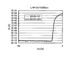
In the TEG, a thin film transistor having L / W = 3 µm / 10000 µm formed by connecting 200 transistors having L / W = 3 µm / 50 µm (film thickness d: 30 nm) in parallel was formed. The initial characteristics of the transistor are shown in FIG. In order to measure the initial characteristic of the transistor, the substrate temperature was cooled to room temperature, and the source-drain (hereinafter referred to as the drain voltage or VD) human voltage to 10 V and the source-called gate voltage (gate voltage or V G ), The change in the characteristics of the source-drain current (hereinafter referred to as drain current or I D ), that is, the V G -I D characteristic, was measured under the condition of changing from -20 V to +20 V. In this case, V G -I D characteristic of a measurement result, V G represents the range of -20 to + 5 V V~.
As shown in Fig. 14, in the transistor having a channel width W of 10000 mu, the off current is 1 × 10 −13 A or less in both V D of 1 V and 10 V, and the measuring instrument (semiconductor parameter analyzer, Agilent 4156C; manufactured by Agilent Technologies Inc.), has a resolution of 100 fA or less. This off-current value corresponds to 10 aA / μm in terms of channel width of 1 μm.
In the present specification, the off current (also referred to as leakage current) is any range of -20 V or more and -5 V or less at room temperature when the threshold value Vth of the n-channel transistor is positive. It indicates the current flowing between the source and the drain of the n-channel transistor when the gate voltage is applied. In addition, room temperature shall be 15 degrees or more and 25 degrees or less. In the transistor using the oxide semiconductor disclosed herein, the current value per unit channel width (W) is 100 aA / μm or less, preferably 1 aA / μm or less, and more preferably 10 zA / μm or less at room temperature. .
In addition, if the value of the off current and the drain voltage is known, the resistance value (off resistance R) when the transistor is in the off state can be calculated from Ohm's law, and the cross-sectional area A and the channel of the channel formation region are calculated. If the length L is known, the off resistivity ρ can also be calculated from the formula ρ = RA / L (R represents an off resistance). The off resistivity obtained from FIG. 14 was 1 × 10 9 Ω · m or more (or 1 × 10 10 Ω · m or more). Here, the cross-sectional area A can be calculated from A = dW when the film thickness of the channel formation region is d and the channel width is W. In general, the boundary between the resistivity of the semiconductor and the insulator is about 1 × 10 5 Ω · m. That is, a transistor using an intrinsic or substantially intrinsic oxide semiconductor according to one aspect of the present invention exhibits a resistivity equivalent to that of an insulator in an off state. From this, it can be understood that this transistor has a heterogeneous effect as a switch element.
The energy gap of the oxide semiconductor is 2 eV or more, preferably 2.5 eV or more, more preferably 3 eV or more.
In addition, a transistor using a high purity oxide semiconductor has good temperature characteristics. Typically, in the current voltage characteristics of the transistor in the temperature range of −25 ° C. to 150 ° C., variations in on current, off current, field effect mobility, subthreshold value (S value), and threshold voltage are almost unchanged. No deterioration of the current voltage characteristic due to temperature is observed.
Next, hot carrier deterioration of a transistor using an oxide semiconductor will be described.
Hot carrier degradation refers to a threshold voltage caused by a phenomenon in which electrons accelerated at high speed are injected into the gate insulating film from a channel near the drain and become fixed charges, or electrons accelerated at high speed form trap levels at the gate insulating film interface. Deterioration of transistor characteristics such as fluctuations and generation of gate leakage current occurs. Factors of hot carrier deterioration include channel hot electron injection (CHE injection) and drain avalanche hot carrier injection (DAHC injection).
Since silicon has a small band gap of 1.12 eV, electrons tend to generate like an avalanche due to avalanche breakdown, and the number of electrons accelerated at a high speed enough to cross the barrier to the gate insulating film increases. On the other hand, the oxide semiconductor shown in the present embodiment has a wide band gap of 3.15 eV, so that avalanche breakdown is less likely to occur, and the resistance to hot carrier deterioration is higher than that of silicon.
In addition, although the band gap of silicon carbide, which is one of the high breakdown voltage materials, and the band gap of the oxide semiconductor are equal, electrons are less likely to be accelerated because the oxide semiconductor has a mobility of about two orders of magnitude smaller than that of silicon carbide. In the case where silicon oxide is used as the gate insulating film using a material containing indium (In) or zinc (Zn), since the barrier between the oxide semiconductor and silicon oxide is larger than silicon carbide, gallium nitride, and silicon, Very few electrons are injected, so that hot carrier deterioration is less likely to occur than silicon carbide, gallium nitride, and silicon, and the drain breakdown voltage is high. Therefore, there is no need to intentionally form a low concentration impurity region between the oxide semiconductor functioning as a channel, the source electrode, and the drain electrode, and the transistor structure becomes very simple, and the number of manufacturing steps can be reduced.
As described above, the transistor using the oxide semiconductor has a high drain breakdown voltage, and specifically, it is possible to have a drain breakdown voltage of 100 V or more, preferably 500 V or more, more preferably 1 kV or more.
This embodiment can be implemented in appropriate combination with any of the other embodiments.
(Embodiment 2)
In this embodiment, an example of the structure for performing multi-gradation display is demonstrated.
The ability to perform multi-gradation display largely depends on the capability of converting digital data from the source driver to analog data (gradation voltage).
In general, in a source driver that processes two bits of digital data, the source driver can display 2 2 = 4 gray levels, if 8 bits, can display 2 8 = 256 gray levels, and if m bits, 2 m gradation can be displayed.
However, in order to increase the capability of the source driver, the circuit configuration of the source driver becomes complicated and the layout area becomes large.
Therefore, in this embodiment, the structure which performs multi-gradation display, without complicating a source driver is demonstrated.
In the present embodiment, among the m-bit digital data to be input, n-bit digital data represents gray scale by voltage gray scale, and the remaining (m-n) bits of digital data express gray scale by time gray scale. By doing in this way, in the source driver which performs the voltage gradation for n bits, it becomes possible to display the gradation for m bits, and multi-gradation display can be performed without complicating a source driver. In addition, m and n are both positive integers and let m> n.
Below, an example of the structure which combines a voltage grayscale and time grayscale is demonstrated. Here, 4 bits (m = 4) of digital data are input, and 2 bits of digital data (n = 2) are used for voltage gray scale, and 2 bits of digital data (m-n = 2) are used for time. A case of using for gradation will be described. However, m and n are not limited.
First, the structure of the display apparatus of this embodiment is demonstrated using FIG. The display device has a
Since the
The
Here, the gradation display method of the display device in this embodiment is demonstrated using FIG. The input digital data is 4 bits and has 16 gray levels of information. The voltage level V L is the lowest voltage level input to the source driver, and the voltage level V H is the highest voltage level input to the source driver.
In this embodiment, since two bits of digital data are used for voltage gradation, three voltage levels are set such that voltage levels adjacent to each other are substantially equal between voltage level V H and voltage level V L. In this way, voltage levels of four gray levels are represented. The difference between the adjacent voltage levels is denoted by α, and α = (V H -V L ) / 4.
Therefore, the voltage level at which the source driver output is the V L when the digital data (00), when the digital data (01) and a V L + α, the
In this way, the voltage levels that the source driver can output are four types: V L , (V L + α), (V L + 2α), and (V L + 3α). That is, when n bits of digital data among m bits of digital data are used for voltage gray level, the source driver can
Therefore, in this embodiment, in order to increase the number of gray scales that can be displayed on the display device, a method of combining time gray scales with voltage gray scales is used. The method of time gradation in the present embodiment will be described below.
First, the display device of the present embodiment implements a so-called line sequential driving method for simultaneously driving pixels for one line. In other words, analog gradation voltages are simultaneously written to one line of pixels. The period in which the analog gradation voltage is written to all the pixels in the pixel portion is called one frame period.
Then, one frame period is divided into a plurality of periods (called a sub frame period). Then, in each sub frame period, line sequential driving is performed to write analog gray voltages to all the pixels. The average value of the analog gradation voltages written in each sub frame period is taken, and gradation display is performed at the voltage level of this average value. In this embodiment, one frame period is divided into four sub frame periods (first to fourth sub frame periods).
That is, by using two bits for time gradation, the difference? Of the voltage levels can be divided almost equally by two bits of digital data, thereby increasing the number of gradations. Therefore, when (m-n) bits of digital data of m bits of digital data are used for time gradation, one frame period is divided into 2 m-n sub frame periods.
Then, by combining the time gray scale with the voltage gray scale, VL, VL + α / 4, VL + 2α / 4, VL + 3α / 4, VL + α, VL + 5α / 4, VL + 6α / 4, VL + 7α / 4, VL + 2α, VL + 9α / 4, VL + 10α / 4, VL + 11α The display corresponding to the voltage level of / 4 and VL + 3α can be realized (see FIG. 3).
An example of a method of performing data processing by combining voltage grayscale and time grayscale is shown below.
In FIG. 2,
Then, the
Then, one frame period is divided into four and four sub frame periods (a first
Here, the number of readings of the
For example, the
The source driver is (V L + 2α) or (V L ) which are analog gray voltages according to the
In addition, also in the case where any of the
In addition, when the digital data of the upper bit of the input
In this way, by combining the voltage grayscale and the time grayscale, gray scale display corresponding to 4 bits can be performed by the
However, even when multi-gradation is performed by the data processing of the present embodiment, it is difficult to display a desired gray scale when the gray scale characteristic of the pixel is low because the off current of the transistor is large. In that case, since the gray scale characteristic is improved by configuring the pixel with the transistor using the oxide semiconductor shown in the first embodiment, display at the voltage level generated by data processing becomes possible.
In addition, when performing the data processing of this embodiment, when the data writing time to a pixel becomes long, an operation speed may become slow. When dividing one frame period into four as in the present embodiment, it is required to multiply the write time by four times. At this time, since the transistor using the oxide semiconductor has a mobility of 10 cm 2 / Vs or more, the writing time can be shortened.
That is, the combination of
This embodiment can be implemented in appropriate combination with any of the other embodiments.
(Embodiment 3)
In this embodiment, the structure of a semiconductor device and an example of the manufacturing method are demonstrated.
An example of the planar structure of a semiconductor device is shown to FIG. 6 (A). 6B is an example of the cross-sectional structure of a semiconductor device, and shows the cross section in the line C1-C2 of FIG. 6 (A). The semiconductor device has a
The
The
Next, the process of manufacturing the
First, an insulating
It is necessary that the board |
Specific examples of the
The insulating
As the method for forming the insulating
In this embodiment, the silicon oxide layer is formed into a film by the sputtering method as the insulating
As an example of the film forming conditions of the insulating
The sputtering gas uses a high purity gas in which hydrogen and the like are removed to a concentration of about ppm level, preferably ppb level.
In addition, it is preferable that hydrogen or the like is not contained in the insulating
In order to remove residual moisture in the film formation chamber, an adsorption type vacuum pump may be used. For example, a cryopump, an ion pump, a titanium servation pump can be used. In particular, the cryopump has a high effect of exhausting hydrogen and the like from the deposition chamber. Therefore, hydrogen etc. in the insulating
As the sputtering method, there are an RF sputtering method using a high frequency power source for the sputtering power supply, a DC sputtering method using a DC power supply, and a pulsed DC sputtering method that gives a pulse bias. The RF sputtering method is mainly used for forming an insulating film, and the DC sputtering method is mainly used for forming a metal film.
Moreover, you may use a multiple sputtering apparatus. The multiple sputtering apparatus can provide the several target from which material differs, and can sputter | spatter multiple target simultaneously or separately in the same film-forming chamber. For example, by sputtering a plurality of targets simultaneously, a film made of a plurality of materials can be formed. In addition, by sputtering separately, a plurality of films having different materials can be laminated.
Moreover, you may use the sputtering apparatus using the magnetron sputtering method. This sputtering apparatus is equipped with the magnet mechanism in the film-forming chamber. Moreover, you may use the sputtering apparatus which uses ECR sputtering method. This sputtering apparatus uses the plasma generated using the microwave.
In addition, you may use the reactive sputtering method as a film-forming method. This sputtering method is a method of chemically reacting a target and a sputtering gas during film-forming, and forming these compound thin films. In addition, you may use the bias sputtering method. This sputtering method is a method of applying a voltage to a substrate during film formation.
As the insulating
Lamination | stacking of a nitride insulation layer and an oxide insulation layer is formed by the following method, for example. First, the sputtering gas containing high purity nitrogen is introduce | transduced into a film-forming chamber, and a silicon nitride layer is formed into a film using a silicon target. Thereafter, the sputtering gas is switched to one containing high purity oxygen to form a silicon oxide layer. As described above, it is preferable to form a silicon nitride layer or a silicon oxide layer while removing residual moisture in the film formation chamber. In addition, you may heat a board | substrate at the time of film-forming.
Next, an oxide semiconductor layer is formed on the insulating
It is preferable not to contain hydrogen etc. as much as possible in an oxide semiconductor layer. Therefore, it is preferable to preheat the board |
As a pretreatment for film formation, argon gas is also introduced to generate plasma to remove dust adhering to the surface of the insulating
As a target of an oxide semiconductor layer, the target of the metal oxide which has zinc oxide as a main component can be used. For example, as a composition ratio, a target of In 2 O 3 : Ga 2 O 3 : ZnO = 1: 1: 1 [mol%], that is, In: Ga: Zn = 1: 1: 1: 0.5 [atom%] can be used. have. In addition, a target having a composition ratio of In: Ga: Zn = 1: 1: 1 [atom%] or In: Ga: Zn = 1: 1: 1 [atom%] can also be used. In addition, it is also possible to use a target containing 10 wt% or less than 2% by weight of SiO 2. The filling rate of the metal oxide in the target is 90% or more and 100% or less, preferably 95% or more and 99.9% or less. By using the target with a high filling rate, the
In addition, when forming an oxide semiconductor layer, it is good to set it as a rare gas (typically argon) atmosphere, oxygen atmosphere, or a rare gas and oxygen mixed atmosphere. As the sputtering gas used for forming the oxide semiconductor layer, a high purity gas in which hydrogen or the like has been removed to a concentration of ppm level, preferably ppb level, is used.
Moreover, it is preferable to remove hydrogen etc. in an oxide semiconductor layer by removing residual moisture in a film-forming chamber. As described above, hydrogen and the like in the oxide semiconductor layer can be reduced as much as possible by exhausting hydrogen and the like in the deposition chamber using a cryo pump. In addition, room temperature may be sufficient as the board | substrate at the time of film-forming, and you may heat to the temperature below 400 degreeC. In addition, it is preferable to keep the deposition chamber at a reduced pressure.
As an example of the film forming conditions of the oxide semiconductor layer, the composition ratio of the target is set to In 2 O 3 : Ga 2 O 3 : ZnO = 1: 1: 1 [mol%], and the substrate temperature is room temperature and the distance between T-S is 110. mm, pressure 0.4 Pa, direct current (DC) power supply 0.5 kW, and sputtering gas are made into the mixed gas of oxygen and argon (oxygen flow rate 15 sccm:
In the above, a compound layer (also referred to as In-Ga-Zn-O) containing indium, gallium, zinc and oxygen was used as the oxide semiconductor layer. In addition, In-Sn-Ga-Zn-O, In-Sn- Zn-O, In-Al-Zn-O, Sn-Ga-Zn-O, Al-Ga-Zn-O, Sn-Al-Zn-O, In-Zn-O, Sn-Zn-O, Al- Zn-O, Zn-Mg-O, Sn-Mg-O, In-Mg-O, In-O, Sn-O, Zn-O, etc. can be used. In addition, the oxide semiconductor layer may contain Si. In addition, such an oxide semiconductor layer may be amorphous or crystalline. Alternatively, non-single crystal may be used or single crystal may be used.
Further, as the oxide semiconductor layer may use a compound represented by InMO 3 (ZnO) m (m > 0). Here, M is one or a plurality of metal elements selected from Ga, Al, Mn and Co. For example, Ga, Ga and Al, Ga and Mn, or Ga and Co may be mentioned as M.
Next, the oxide semiconductor layer is etched through the first photolithography method and processed into an island-shaped oxide semiconductor layer 412 (see FIG. 7A). Moreover, you may form the resist used for a process by the inkjet method. When the resist is formed by the inkjet method, no photomask is used, and thus manufacturing cost can be reduced.
Moreover, you may form a resist using a multi-gradation photomask. The multi-gradation photomask is a mask that can be exposed at a multilevel light intensity (light intensity). By using a multi-gradation photomask, the number of photomasks can be reduced.
In addition, dry etching or wet etching may be sufficient as etching of an oxide semiconductor layer, and both may be used.
When dry etching is carried out, a parallel plate-type reactive ion etching (RIE) method or an inductively coupled plasma (ICP) etching method can be used. (The amount of power applied to the coil-shaped electrode, the amount of power applied to the electrode on the substrate side, the electrode temperature on the substrate side, and the like) are appropriately controlled so that etching can be performed with a desired processing shape.
As an etching gas used for dry etching, a gas containing chlorine (chlorine-based gas such as chlorine, boron chloride, silicon chloride, carbon tetrachloride, etc.) is preferable, but a gas containing fluorine (fluorine-based gas such as tetrafluoride) Carbon, sulfur fluoride, nitrogen fluoride, trifluoromethane, etc.), hydrogen bromide, oxygen, or a gas in which rare gas such as helium or argon is added to these gases.
As an etchant used for wet etching, a solution obtained by mixing phosphoric acid, acetic acid and nitric acid, ammonia perwater (31 wt% hydrogen peroxide: 28 wt% ammonia: water = 5: 2: 2), and the like can be used. Moreover, you may use ITO-07N (made by KANTO CHEMICAL CO., INC.). What is necessary is just to adjust suitably according to the material of an oxide semiconductor about the conditions of etching (etching liquid, etching time, temperature, etc.).
In addition, when performing wet etching, etching liquid is removed by washing with the material etched. The waste liquid of the etching liquid containing this removed material may be refine | purified, and the contained material may be reused. The resources can be efficiently utilized by recovering and reusing materials (for example, rare metals such as indium) contained in the oxide semiconductor layer from the waste liquid after the etching.
In this embodiment, the oxide semiconductor layer is processed into an island-shaped
Next, a first heat treatment is performed on the
The heat treatment apparatus is not limited to an electric furnace, and an apparatus for heating by heat conduction or heat radiation from a heating element (for example, a resistive heating element or the like) may be used. For example, a Rapid Thermal Annealing (RTA) device such as a Gas Rapid Thermal Annealing (GRTA) device or a Lamp Rapid Thermal Annealing (LRTA) device may be used.
The LRTA apparatus is a device that heats by radiation of light (electromagnetic waves) emitted from lamps such as halogen lamps, metal halide lamps, xenon arc lamps, carbon arc lamps, high pressure sodium lamps, and high pressure mercury lamps.
A GRTA apparatus is an apparatus which heats using high temperature gas. As the gas, an inert gas (typically a rare gas such as argon) or nitrogen gas can be used.
For example, when performing a 1st heat processing using a GRTA apparatus, after heating a board | substrate in inert gas of high temperature (for example, 650 degreeC-700 degreeC) for several minutes, it is good to take out from this inert gas. By using the GRTA apparatus, the high temperature heat treatment in a short time becomes possible.
It is preferable not to contain hydrogen etc. in the atmosphere at the time of a 1st heat processing. Alternatively, the purity of gases such as nitrogen, helium, neon, and argon introduced into the heat treatment device is preferably 6N (99.9999%) or more, more preferably 7N (99.99999%) or more, that is, impurity concentration is 1 ppm. Or less, preferably 0.1 ppm or less).
In addition, depending on the conditions of the first heat treatment or the material of the
For example, the
In addition, you may perform a 1st heat processing with respect to an oxide semiconductor layer before processing into an island shape oxide semiconductor layer. In this case, after a 1st heat processing, a 1st photolithography process is performed and it processes to island shape.
In addition, you may perform a 1st heat processing in a later process. For example, the source electrode and the drain electrode may be formed on the
Although the primary purpose of the first heat treatment is to remove hydrogen or the like from the
As described above, hydrogen or the like can be removed from the oxide semiconductor layer by the first heat treatment. That is, the first heat treatment obtains the effects of dehydration and dehydrogenation of the oxide semiconductor layer.
Next, a conductive film is formed over the insulating
The conductive film may be formed by sputtering or vacuum evaporation. As a material of a conductive film, metal materials, such as Al, Cu, Cr, Ta, Ti, Mo, W, Y, the alloy material which uses this metal material as a component, the metal oxide which has electroconductivity, etc. are mentioned. In addition, for example, in order to prevent the occurrence of hillock or whisker, an Al material to which elements such as Si, Ti, Ta, W, Mo, Cr, Nd, Sc, and Y may be added may be used. Can be improved. As the conductive metal oxide, indium oxide, tin oxide, zinc oxide, indium tin oxide alloy (ITO), indium zinc oxide alloy (IZO), or one containing silicon or silicon oxide in the metal oxide material can be used. .
The conductive film may have a single layer structure or a laminated structure of two or more layers. For example, the single-layered structure of the aluminum film containing silicon, the two-layered structure which laminated | stacked the titanium film on the aluminum film, and the three-layered structure which laminated | stacked the aluminum film superimposed on the titanium film, and laminated | stacked the titanium film on it are mentioned. Moreover, it is good also as a structure which the metal layers, such as Al and Cu, and the high melting point metal layers, such as Cr, Ta, Ti, Mo, and W, were laminated | stacked.
In this embodiment, a titanium film having a thickness of 150 nm is formed as a conductive film by sputtering.
Next, a resist is formed on the conductive film by a second photolithography step and is selectively etched to form the
The
Moreover, you may form the resist for forming the
In addition, it is necessary to prevent the
For example, In-Ga-Zn-O is used as the
In addition, by adjusting the etching conditions, a part of the
In addition, KrF laser light, ArF laser light, etc. may be used for exposure at the time of forming a resist. In addition, by using ultra-ultraviolet rays (wavelength: several nm to several 10 nm), the resolution at the time of exposure can be made high and the depth of focus can be increased, and fine processing can be performed.
Here, as shown in FIG. 6B, the channel length of the
After the
Next, a
The
When forming the
As an example of the film forming conditions of the
Next, a resist is formed by a third photolithography step and is selectively etched to remove a part of the
Next, after forming a conductive film on the
The
Specific examples of the two-layer structure of the
As a specific example of the three-layer structure, a structure in which a tungsten layer (or tungsten nitride layer), an alloy layer of aluminum and silicon (or an alloy layer of aluminum and titanium), and a titanium nitride layer (or titanium layer) are laminated is mentioned. Can be. In addition, the gate electrode may be formed using a light-transmitting conductive film. As an example of the electrically conductive film which has light transmissivity, the electroconductive oxide which has light transparency is mentioned.
In this embodiment, a titanium film having a thickness of 150 nm formed by the sputtering method is used as the
Next, a second heat treatment (preferably between 200 ° C. and 400 ° C., for example, 250 ° C. and 350 ° C. or less) is performed under an inert gas atmosphere or an oxygen gas atmosphere. In the present embodiment, the second heat treatment is performed at 250 ° C. for one hour in a nitrogen atmosphere. By the second heat treatment, hydrogen and the like in the
Moreover, you may heat-process in 100 degreeC or more and 200 degrees C or less, 1 hour or more and 30 hours or less in air | atmosphere after a 2nd heat processing. The heat treatment here may be maintained by maintaining a constant heating temperature, or may be repeated by increasing the temperature from room temperature to a heating temperature of 100 ° C. to 200 ° C. and the temperature drop from the heating temperature to room temperature a plurality of times.
Through the above steps, the
In addition, a protective insulating layer or a planarization insulating layer for planarization may be formed over the
As a protective insulating layer, a silicon oxide layer, a silicon nitride layer, a silicon oxynitride layer, a silicon nitride oxide layer, or an aluminum oxide layer can be formed by single layer or lamination.
As the planarization insulating layer, an organic material having heat resistance, such as polyimide, acryl, benzocyclobutene, polyamide, or epoxy, can be used. In addition to the above organic materials, low dielectric constant materials (low-k materials), siloxane resins, PSG (phosphosilicate glass: phosphorus glass), BPSG (borophosphosilicate glass: phosphorus boron glass), and the like may be used. The planarization insulating layer may be formed by stacking a plurality of insulating films formed of these materials.
Here, siloxane resin is corresponded to resin containing the Si-O-Si bond formed from the siloxane material as a starting material. As the substituent, the siloxane-based resin may use an organic group (for example, an alkyl group or an aryl group). In addition, the organic group may have a fluoro group.
The formation method of a planarization insulating layer is not specifically limited, According to the material, methods, such as a sputtering method, the SOG method, the spin coat method, the dip method, the spray coating method, the droplet ejection method (inkjet method, screen printing, offset printing, etc.) In addition, apparatuses, such as a doctor knife, a roll coater, a curtain coater, and a knife coater, can be used.
As described above, a semiconductor device using an intrinsic or substantially intrinsic oxide semiconductor can be manufactured.
This embodiment can be implemented in appropriate combination with any of the other embodiments.
(Fourth Embodiment)
In this embodiment, the structure of a semiconductor device and an example of the manufacturing method are demonstrated.
8E shows an example of the cross-sectional structure of the semiconductor device. The semiconductor device has a
The
For example, the
Hereinafter, a method of manufacturing the
First, the
In addition, an insulating film (for example, a silicon oxide film or a silicon nitride film) serving as a base film may be formed between the
Next, a
Next, an
Here, it is preferable to perform a 1st heat treatment with respect to the
Next, a
Through the above steps, the
In addition, a protective
As the protective insulating
Next, you may perform 2nd heat processing. The second heat treatment may be performed at 200 ° C. or more and 400 ° C. (preferably 250 ° C. or more and 350 ° C. or less) in an inert gas (for example, nitrogen) or oxygen atmosphere. In this embodiment, 250 degreeC and 1 hour of heating are performed in nitrogen atmosphere.
By performing the second heat treatment, hydrogen or the like in the
In addition, the insulating
At the time of forming the protective insulating
As described above, a semiconductor device using an intrinsic or substantially intrinsic oxide semiconductor can be manufactured.
This embodiment can be implemented in appropriate combination with any of the other embodiments.
(Embodiment 5)
In this embodiment, the structure of a semiconductor device and an example of the manufacturing method are demonstrated.
An example of the cross-sectional structure of a semiconductor device is shown to FIG. 9D. The semiconductor device has a
The
The difference from
Hereinafter, a method of manufacturing the
Next, an
As the
As an example of the film forming conditions of the
At this time, it is preferable not to include hydrogen or the like in the
Next, a second heat treatment is performed. The second heat treatment may be performed at 200 ° C. or more and 400 ° C. (preferably 250 ° C. or more and 350 ° C. or less) in an inert gas (for example, nitrogen) or oxygen atmosphere. In this embodiment, 250 degreeC and 1 hour of heating are performed in nitrogen atmosphere.
By performing the second heat treatment, oxygen is supplied from the
On the other hand, in the area | region which is not covered by the
That is, the
Next, the
Through the above steps, the
In addition, a protective
In this embodiment, after hydrogen in the
As a result, in the
As described above, a semiconductor device using an intrinsic or substantially intrinsic oxide semiconductor can be manufactured.
This embodiment can be implemented in appropriate combination with any of the other embodiments.
(Embodiment 6)
In this embodiment, the structure of a semiconductor device and an example of the manufacturing method are shown.
10D illustrates a cross-sectional structure of the semiconductor device. The semiconductor device has a
The
Unlike the fourth embodiment (FIG. 8), the
Hereinafter, a process of fabricating the
On the
Next, an
Through the above steps, the
In addition, an
Next, you may perform 2nd heat processing. The second heat treatment may be performed at 200 ° C. or more and 400 ° C. (preferably 250 ° C. or more and 350 ° C. or less) in an inert gas (for example, nitrogen) or oxygen atmosphere. In this embodiment, 250 degreeC and 1 hour of heating are performed in nitrogen atmosphere.
By the second heat treatment, oxygen can be supplied from the
In addition, the insulating
As described above, a semiconductor device using an intrinsic or substantially intrinsic oxide semiconductor can be manufactured.
This embodiment can be implemented in appropriate combination with any of the other embodiments.
(Seventh Embodiment)
In this embodiment, a specific example of an electronic device including the display device described in the above embodiment will be described. However, the electronic device applicable to this invention is not limited to the specific example shown below.
Fig. 11A is a portable organic group. 11B is a digital camera. 11C is a television receiver. 12A is a computer. Fig. 12B is a mobile phone. 12C is electronic paper. The electronic paper can be used for electronic books (also called electronic books and e-books), posters, and the like. Fig. 12D is a digital photo frame. The display device of one embodiment of the present invention can be used for the
By applying the display device of one embodiment of the present invention to such an electronic device, it is possible to achieve high reliability and low power consumption when displaying a still picture or the like.
This embodiment can be implemented in appropriate combination with any of the other embodiments.
This application is based on a Japanese patent application having a serial number 2009-292630, filed in the Japanese Patent Office on December 24, 2009, which is incorporated by reference in its entirety.
100: display part 101: pixel part
102 : gate driver 103 : source driver
104: transistor 105: liquid crystal element
106: wiring 107: wiring
108: capacitor 200: data processing circuit
201 to 203:
220:
240: Average value 320: Board
322: gate insulating layer 323: protective insulating layer
332:
342: gate insulating layer 343: insulating layer
345: oxide semiconductor layer 346: oxide semiconductor layer
350: transistor 351: gate electrode
355a and 355b: electrode 356: oxide insulating layer
360: transistor 361: gate electrode
362: oxide semiconductor layer 363: channel formation region
364a and 364b:
366: oxide insulating layer 390: transistor
391: gate electrode 393: oxide semiconductor layer
394:
396: protective insulating layer 397: gate insulating layer
398: insulating layer 399: oxide semiconductor layer
400: substrate 402: gate insulating layer
407: insulating layer 410: transistor
411: gate electrode 412: oxide semiconductor layer
415a and 415b:
421a, 421b: Opening 5000: Pixel
5001: Transistor 5002: Liquid Crystal Element
5003 : Capacitor
9630, 9640, 9650, 9660, 9670, 9680, 9690: Housing
9631, 9641, 9651, 9661, 9671, 9681, 9691: Display part
Claims (29)
A pixel portion in which pixels having transistors and display elements are arranged in a matrix;
A gate driver electrically connected to the gate of the transistor,
A source driver electrically connected to the source or drain of the transistor, and
Having a data processing circuit for outputting a signal to the source driver,
The transistor has a channel formation region using an oxide semiconductor,
The data processing circuit uses n-bit (m, n are all positive integers, m > n) of digital data of m bits to be input for voltage gradation, and (m-n) bits of digital data. And output the signal using the time gray scale.
One frame period is divided into (m-n) subframe periods for time gradation.
And the source driver outputs (2 n +1) or less voltage levels.
And the transistor has a mobility of 10 cm 2 / Vs or more.
The transistor is formed on a substrate,
And the transistor has an off-state current of 1 aA / μm or less.
The display device is a liquid crystal device.
The electronic device is selected from the group consisting of a portable game machine, a digital camera, a television receiver, a computer, an electronic paper, and a digital photo frame.
A pixel portion in which pixels having transistors and display elements are arranged in a matrix;
A gate driver electrically connected to the gate of the transistor,
A source driver electrically connected to the source or drain of the transistor, and
Having a data processing circuit for outputting a signal to the source driver,
The transistor has a channel formation region using an intrinsic or substantially intrinsic oxide semiconductor,
The data processing circuit uses n-bit (m, n are all positive integers, m > n) of digital data of m bits to be input for voltage gradation, and (m-n) bits of digital data. And output the signal using the time gray scale.
A display device in which the carrier concentration of the intrinsic or substantially intrinsic oxide semiconductor is less than 1 × 10 14 / cm 3 .
One frame period is divided into (m-n) subframe periods for time gradation.
And the source driver outputs (2 n +1) or less voltage levels.
And the transistor has a mobility of 10 cm 2 / Vs or more.
The transistor is formed on a substrate,
And the transistor has an off-state current of 1 aA / μm or less.
The display device is a liquid crystal device.
The electronic device is selected from the group consisting of a portable organic device, a digital camera, a television receiver, a computer, an electronic paper, and a digital photo frame.
A pixel portion in which pixels having transistors and display elements are arranged in a matrix;
A gate driver electrically connected to the gate of the transistor,
A source driver electrically connected to the source or drain of the transistor, and
Having a data processing circuit for outputting a signal to the source driver,
The transistor uses an oxide semiconductor and has a channel formation region with an off current of 1 aA / μm or less,
The data processing circuit processes n bits (m and n are all positive integers and m > n) of the digital data of the m bits to be input as the data related to the voltage gray level, and (m-n) bits. And display the digital data of the data as data related to time grayscale.
And a carrier concentration of the oxide semiconductor is less than 1 × 10 14 / cm 3 .
One frame period is divided into (m-n) subframe periods for time gradation.
And the source driver outputs (2 n +1) or less voltage levels.
And the transistor has a mobility of 10 cm 2 / Vs or more.
The display device is a liquid crystal device.
The electronic device is selected from the group consisting of a portable organic device, a digital camera, a television receiver, a computer, an electronic paper, and a digital photo frame.
A pixel portion in which pixels having transistors and display elements are arranged in a matrix;
A gate driver electrically connected to the gate of the transistor,
A source driver electrically connected to the source or drain of the transistor, and
Has a data processing circuit,
The transistor has a channel formation region using an oxide semiconductor,
The data processing circuit may be output from the source driver among (n-1) voltage levels based on digital data of n bits (m and n are all positive integers and m > n) among the m bits of digital data to be input. Configured to select two voltage levels,
The data processing circuit is configured to output 2 mn digital data about one pixel in one frame period to the source driver, wherein each of the 2 mn digital data corresponds to two digital levels corresponding to the two voltage levels. A display device selected from any one of data.
One frame period is divided into (m-n) subframe periods.
And the source driver outputs (2 n +1) or less voltage levels.
And the transistor has a mobility of 10 cm 2 / Vs or more.
The transistor is formed on a substrate,
And the transistor has an off current of 1 aA / μm or less.
The display device is a liquid crystal device.
The electronic device is selected from the group consisting of a portable organic device, a digital camera, a television receiver, a computer, an electronic paper, and a digital photo frame.
Applications Claiming Priority (2)
| Application Number | Priority Date | Filing Date | Title |
|---|---|---|---|
| JPJP-P-2009-292630 | 2009-12-24 | ||
| JP2009292630 | 2009-12-24 |
Publications (1)
| Publication Number | Publication Date |
|---|---|
| KR20120101716A true KR20120101716A (en) | 2012-09-14 |
Family
ID=44186925
Family Applications (1)
| Application Number | Title | Priority Date | Filing Date |
|---|---|---|---|
| KR20127018792A KR20120101716A (en) | 2009-12-24 | 2010-11-26 | Display device and electronic device |
Country Status (5)
| Country | Link |
|---|---|
| US (1) | US9047836B2 (en) |
| JP (1) | JP5797896B2 (en) |
| KR (1) | KR20120101716A (en) |
| TW (1) | TWI518664B (en) |
| WO (1) | WO2011077926A1 (en) |
Families Citing this family (15)
| Publication number | Priority date | Publication date | Assignee | Title |
|---|---|---|---|---|
| KR101805378B1 (en) | 2010-01-24 | 2017-12-06 | 가부시키가이샤 한도오따이 에네루기 켄큐쇼 | Display device and manufacturing method thereof |
| WO2012137886A1 (en) * | 2011-04-08 | 2012-10-11 | シャープ株式会社 | Display device, and method for driving display device |
| US9048788B2 (en) | 2011-05-13 | 2015-06-02 | Semiconductor Energy Laboratory Co., Ltd. | Semiconductor device comprising a photoelectric conversion portion |
| US9117916B2 (en) * | 2011-10-13 | 2015-08-25 | Semiconductor Energy Laboratory Co., Ltd. | Semiconductor device comprising oxide semiconductor film |
| US9419146B2 (en) | 2012-01-26 | 2016-08-16 | Semiconductor Energy Laboratory Co., Ltd. | Semiconductor device and method for manufacturing the same |
| KR102099262B1 (en) * | 2012-07-11 | 2020-04-09 | 가부시키가이샤 한도오따이 에네루기 켄큐쇼 | Liquid crystal display device and method for driving the same |
| KR101660196B1 (en) * | 2012-08-24 | 2016-09-26 | 샤프 가부시키가이샤 | Liquid crystal display device and method for driving same |
| JP6025851B2 (en) | 2012-09-13 | 2016-11-16 | シャープ株式会社 | Liquid crystal display |
| CN104620309B (en) | 2012-09-13 | 2017-09-22 | 夏普株式会社 | Liquid crystal display device |
| MY171999A (en) | 2012-10-02 | 2019-11-11 | Sharp Kk | Liquid crystal display device and method for driving same |
| KR20150085035A (en) * | 2012-11-15 | 2015-07-22 | 가부시키가이샤 한도오따이 에네루기 켄큐쇼 | Liquid crystal display device |
| CN105144278B (en) * | 2013-04-23 | 2017-12-26 | 夏普株式会社 | Liquid crystal display device |
| US20160155803A1 (en) * | 2014-11-28 | 2016-06-02 | Semiconductor Energy Laboratory Co., Ltd. | Semiconductor Device, Method for Manufacturing the Semiconductor Device, and Display Device Including the Semiconductor Device |
| US10262570B2 (en) | 2015-03-05 | 2019-04-16 | Semiconductor Energy Laboratory Co., Ltd. | Semiconductor device and method for driving the same |
| JP2017010000A (en) | 2015-04-13 | 2017-01-12 | 株式会社半導体エネルギー研究所 | Display device |
Family Cites Families (135)
| Publication number | Priority date | Publication date | Assignee | Title |
|---|---|---|---|---|
| US3675232A (en) | 1969-05-21 | 1972-07-04 | Gen Electric | Video generator for data display |
| JPS60198861A (en) | 1984-03-23 | 1985-10-08 | Fujitsu Ltd | Thin film transistor |
| JPH0244256B2 (en) | 1987-01-28 | 1990-10-03 | Kagaku Gijutsucho Mukizaishitsu Kenkyushocho | INGAZN2O5DESHIMESARERUROTSUHOSHOKEINOSOJOKOZOOJUSURUKAGOBUTSUOYOBISONOSEIZOHO |
| JPH0244260B2 (en) | 1987-02-24 | 1990-10-03 | Kagaku Gijutsucho Mukizaishitsu Kenkyushocho | INGAZN5O8DESHIMESARERUROTSUHOSHOKEINOSOJOKOZOOJUSURUKAGOBUTSUOYOBISONOSEIZOHO |
| JPS63210023A (en) | 1987-02-24 | 1988-08-31 | Natl Inst For Res In Inorg Mater | Compound having laminar structure of hexagonal crystal system expressed by ingazn4o7 and its production |
| JPH0244258B2 (en) | 1987-02-24 | 1990-10-03 | Kagaku Gijutsucho Mukizaishitsu Kenkyushocho | INGAZN3O6DESHIMESARERUROTSUHOSHOKEINOSOJOKOZOOJUSURUKAGOBUTSUOYOBISONOSEIZOHO |
| JPH0244262B2 (en) | 1987-02-27 | 1990-10-03 | Kagaku Gijutsucho Mukizaishitsu Kenkyushocho | INGAZN6O9DESHIMESARERUROTSUHOSHOKEINOSOJOKOZOOJUSURUKAGOBUTSUOYOBISONOSEIZOHO |
| JPH0244263B2 (en) | 1987-04-22 | 1990-10-03 | Kagaku Gijutsucho Mukizaishitsu Kenkyushocho | INGAZN7O10DESHIMESARERUROTSUHOSHOKEINOSOJOKOZOOJUSURUKAGOBUTSUOYOBISONOSEIZOHO |
| JPH0652470B2 (en) | 1988-09-14 | 1994-07-06 | インターナショナル・ビジネス・マシーンズ・コーポレーション | Method and apparatus for color conversion |
| US5122792A (en) | 1990-06-21 | 1992-06-16 | David Sarnoff Research Center, Inc. | Electronic time vernier circuit |
| JPH0772824B2 (en) | 1991-12-03 | 1995-08-02 | インターナショナル・ビジネス・マシーンズ・コーポレイション | Display system |
| JPH05251705A (en) | 1992-03-04 | 1993-09-28 | Fuji Xerox Co Ltd | Thin-film transistor |
| JP3471928B2 (en) * | 1994-10-07 | 2003-12-02 | 株式会社半導体エネルギー研究所 | Driving method of active matrix display device |
| JP3479375B2 (en) | 1995-03-27 | 2003-12-15 | 科学技術振興事業団 | Metal oxide semiconductor device in which a pn junction is formed with a thin film transistor made of a metal oxide semiconductor such as cuprous oxide, and methods for manufacturing the same |
| DE69635107D1 (en) | 1995-08-03 | 2005-09-29 | Koninkl Philips Electronics Nv | SEMICONDUCTOR ARRANGEMENT WITH A TRANSPARENT CIRCUIT ELEMENT |
| KR100337866B1 (en) | 1995-09-06 | 2002-11-04 | 삼성에스디아이 주식회사 | Method for driving grey scale display of matrix-type liquid crystal display device |
| US5892496A (en) | 1995-12-21 | 1999-04-06 | Advanced Micro Devices, Inc. | Method and apparatus for displaying grayscale data on a monochrome graphic display |
| JP3625598B2 (en) | 1995-12-30 | 2005-03-02 | 三星電子株式会社 | Manufacturing method of liquid crystal display device |
| US6184874B1 (en) | 1997-11-19 | 2001-02-06 | Motorola, Inc. | Method for driving a flat panel display |
| JP4170454B2 (en) | 1998-07-24 | 2008-10-22 | Hoya株式会社 | Article having transparent conductive oxide thin film and method for producing the same |
| US6292168B1 (en) | 1998-08-13 | 2001-09-18 | Xerox Corporation | Period-based bit conversion method and apparatus for digital image processing |
| JP2000150861A (en) | 1998-11-16 | 2000-05-30 | Tdk Corp | Oxide thin film |
| JP3276930B2 (en) | 1998-11-17 | 2002-04-22 | 科学技術振興事業団 | Transistor and semiconductor device |
| JP4637315B2 (en) | 1999-02-24 | 2011-02-23 | 株式会社半導体エネルギー研究所 | Display device |
| US7193594B1 (en) | 1999-03-18 | 2007-03-20 | Semiconductor Energy Laboratory Co., Ltd. | Display device |
| US7145536B1 (en) * | 1999-03-26 | 2006-12-05 | Semiconductor Energy Laboratory Co., Ltd. | Liquid crystal display device |
| US6952194B1 (en) * | 1999-03-31 | 2005-10-04 | Semiconductor Energy Laboratory Co., Ltd. | Liquid crystal display device |
| US6753854B1 (en) * | 1999-04-28 | 2004-06-22 | Semiconductor Energy Laboratory Co., Ltd. | Display device |
| TW460731B (en) | 1999-09-03 | 2001-10-21 | Ind Tech Res Inst | Electrode structure and production method of wide viewing angle LCD |
| TW472277B (en) * | 1999-10-04 | 2002-01-11 | Matsushita Electric Ind Co Ltd | Driving method of display panel, luminance compensation device for display panel and driving device |
| JP4089858B2 (en) | 2000-09-01 | 2008-05-28 | 国立大学法人東北大学 | Semiconductor device |
| KR20020038482A (en) | 2000-11-15 | 2002-05-23 | 모리시타 요이찌 | Thin film transistor array, method for producing the same, and display panel using the same |
| JP3997731B2 (en) | 2001-03-19 | 2007-10-24 | 富士ゼロックス株式会社 | Method for forming a crystalline semiconductor thin film on a substrate |
| JP2002289859A (en) | 2001-03-23 | 2002-10-04 | Minolta Co Ltd | Thin-film transistor |
| KR100769168B1 (en) * | 2001-09-04 | 2007-10-23 | 엘지.필립스 엘시디 주식회사 | Method and Apparatus For Driving Liquid Crystal Display |
| JP3925839B2 (en) | 2001-09-10 | 2007-06-06 | シャープ株式会社 | Semiconductor memory device and test method thereof |
| JP4090716B2 (en) | 2001-09-10 | 2008-05-28 | 雅司 川崎 | Thin film transistor and matrix display device |
| JP4164562B2 (en) | 2002-09-11 | 2008-10-15 | 独立行政法人科学技術振興機構 | Transparent thin film field effect transistor using homologous thin film as active layer |
| US7061014B2 (en) | 2001-11-05 | 2006-06-13 | Japan Science And Technology Agency | Natural-superlattice homologous single crystal thin film, method for preparation thereof, and device using said single crystal thin film |
| JP4083486B2 (en) | 2002-02-21 | 2008-04-30 | 独立行政法人科学技術振興機構 | Method for producing LnCuO (S, Se, Te) single crystal thin film |
| CN1445821A (en) | 2002-03-15 | 2003-10-01 | 三洋电机株式会社 | Forming method of ZnO film and ZnO semiconductor layer, semiconductor element and manufacturing method thereof |
| JP3933591B2 (en) | 2002-03-26 | 2007-06-20 | 淳二 城戸 | Organic electroluminescent device |
| US7339187B2 (en) | 2002-05-21 | 2008-03-04 | State Of Oregon Acting By And Through The Oregon State Board Of Higher Education On Behalf Of Oregon State University | Transistor structures |
| JP2004022625A (en) | 2002-06-13 | 2004-01-22 | Murata Mfg Co Ltd | Manufacturing method of semiconductor device and its manufacturing method |
| US7105868B2 (en) | 2002-06-24 | 2006-09-12 | Cermet, Inc. | High-electron mobility transistor with zinc oxide |
| US7067843B2 (en) | 2002-10-11 | 2006-06-27 | E. I. Du Pont De Nemours And Company | Transparent oxide semiconductor thin film transistors |
| JP4166105B2 (en) | 2003-03-06 | 2008-10-15 | シャープ株式会社 | Semiconductor device and manufacturing method thereof |
| JP2004273732A (en) | 2003-03-07 | 2004-09-30 | Sharp Corp | Active matrix substrate and its producing process |
| JP4108633B2 (en) | 2003-06-20 | 2008-06-25 | シャープ株式会社 | THIN FILM TRANSISTOR, MANUFACTURING METHOD THEREOF, AND ELECTRONIC DEVICE |
| US7262463B2 (en) | 2003-07-25 | 2007-08-28 | Hewlett-Packard Development Company, L.P. | Transistor including a deposited channel region having a doped portion |
| WO2005088726A1 (en) | 2004-03-12 | 2005-09-22 | Japan Science And Technology Agency | Amorphous oxide and thin film transistor |
| US7297977B2 (en) | 2004-03-12 | 2007-11-20 | Hewlett-Packard Development Company, L.P. | Semiconductor device |
| US7282782B2 (en) | 2004-03-12 | 2007-10-16 | Hewlett-Packard Development Company, L.P. | Combined binary oxide semiconductor device |
| US7145174B2 (en) | 2004-03-12 | 2006-12-05 | Hewlett-Packard Development Company, Lp. | Semiconductor device |
| US7211825B2 (en) | 2004-06-14 | 2007-05-01 | Yi-Chi Shih | Indium oxide-based thin film transistors and circuits |
| JP2006100760A (en) | 2004-09-02 | 2006-04-13 | Casio Comput Co Ltd | Thin-film transistor and its manufacturing method |
| US7285501B2 (en) | 2004-09-17 | 2007-10-23 | Hewlett-Packard Development Company, L.P. | Method of forming a solution processed device |
| US7298084B2 (en) | 2004-11-02 | 2007-11-20 | 3M Innovative Properties Company | Methods and displays utilizing integrated zinc oxide row and column drivers in conjunction with organic light emitting diodes |
| US7863611B2 (en) | 2004-11-10 | 2011-01-04 | Canon Kabushiki Kaisha | Integrated circuits utilizing amorphous oxides |
| US7791072B2 (en) | 2004-11-10 | 2010-09-07 | Canon Kabushiki Kaisha | Display |
| BRPI0517560B8 (en) | 2004-11-10 | 2018-12-11 | Canon Kk | field effect transistor |
| RU2358354C2 (en) | 2004-11-10 | 2009-06-10 | Кэнон Кабусики Кайся | Light-emitting device |
| US7829444B2 (en) | 2004-11-10 | 2010-11-09 | Canon Kabushiki Kaisha | Field effect transistor manufacturing method |
| CA2585190A1 (en) | 2004-11-10 | 2006-05-18 | Canon Kabushiki Kaisha | Amorphous oxide and field effect transistor |
| US7453065B2 (en) | 2004-11-10 | 2008-11-18 | Canon Kabushiki Kaisha | Sensor and image pickup device |
| US7579224B2 (en) | 2005-01-21 | 2009-08-25 | Semiconductor Energy Laboratory Co., Ltd. | Method for manufacturing a thin film semiconductor device |
| TWI505473B (en) | 2005-01-28 | 2015-10-21 | Semiconductor Energy Lab | Semiconductor device, electronic device, and method of manufacturing semiconductor device |
| JP4777078B2 (en) | 2005-01-28 | 2011-09-21 | 株式会社半導体エネルギー研究所 | Method for manufacturing semiconductor device |
| TWI390735B (en) | 2005-01-28 | 2013-03-21 | Semiconductor Energy Lab | Semiconductor device, electronic device, and method of manufacturing semiconductor device |
| US7858451B2 (en) | 2005-02-03 | 2010-12-28 | Semiconductor Energy Laboratory Co., Ltd. | Electronic device, semiconductor device and manufacturing method thereof |
| US7948171B2 (en) | 2005-02-18 | 2011-05-24 | Semiconductor Energy Laboratory Co., Ltd. | Light emitting device |
| US20060197092A1 (en) | 2005-03-03 | 2006-09-07 | Randy Hoffman | System and method for forming conductive material on a substrate |
| US8681077B2 (en) | 2005-03-18 | 2014-03-25 | Semiconductor Energy Laboratory Co., Ltd. | Semiconductor device, and display device, driving method and electronic apparatus thereof |
| WO2006105077A2 (en) | 2005-03-28 | 2006-10-05 | Massachusetts Institute Of Technology | Low voltage thin film transistor with high-k dielectric material |
| US7645478B2 (en) | 2005-03-31 | 2010-01-12 | 3M Innovative Properties Company | Methods of making displays |
| US8300031B2 (en) | 2005-04-20 | 2012-10-30 | Semiconductor Energy Laboratory Co., Ltd. | Semiconductor device comprising transistor having gate and drain connected through a current-voltage conversion element |
| JP2006344849A (en) | 2005-06-10 | 2006-12-21 | Casio Comput Co Ltd | Thin film transistor |
| US7691666B2 (en) | 2005-06-16 | 2010-04-06 | Eastman Kodak Company | Methods of making thin film transistors comprising zinc-oxide-based semiconductor materials and transistors made thereby |
| US7402506B2 (en) | 2005-06-16 | 2008-07-22 | Eastman Kodak Company | Methods of making thin film transistors comprising zinc-oxide-based semiconductor materials and transistors made thereby |
| US7507618B2 (en) | 2005-06-27 | 2009-03-24 | 3M Innovative Properties Company | Method for making electronic devices using metal oxide nanoparticles |
| KR100711890B1 (en) | 2005-07-28 | 2007-04-25 | 삼성에스디아이 주식회사 | Organic Light Emitting Display and Fabrication Method for the same |
| JP2007059128A (en) | 2005-08-23 | 2007-03-08 | Canon Inc | Organic electroluminescent display device and manufacturing method thereof |
| JP2007073558A (en) | 2005-09-02 | 2007-03-22 | Kochi Prefecture Sangyo Shinko Center | Method of manufacturing thin-film transistor |
| JP4560502B2 (en) * | 2005-09-06 | 2010-10-13 | キヤノン株式会社 | Field effect transistor |
| JP5116225B2 (en) | 2005-09-06 | 2013-01-09 | キヤノン株式会社 | Manufacturing method of oxide semiconductor device |
| JP4280736B2 (en) | 2005-09-06 | 2009-06-17 | キヤノン株式会社 | Semiconductor element |
| JP2007073705A (en) | 2005-09-06 | 2007-03-22 | Canon Inc | Oxide-semiconductor channel film transistor and its method of manufacturing same |
| JP4850457B2 (en) | 2005-09-06 | 2012-01-11 | キヤノン株式会社 | Thin film transistor and thin film diode |
| EP1998373A3 (en) | 2005-09-29 | 2012-10-31 | Semiconductor Energy Laboratory Co, Ltd. | Semiconductor device having oxide semiconductor layer and manufacturing method thereof |
| JP2007109918A (en) | 2005-10-14 | 2007-04-26 | Toppan Printing Co Ltd | Transistor and its manufacturing method |
| JP5037808B2 (en) | 2005-10-20 | 2012-10-03 | キヤノン株式会社 | Field effect transistor using amorphous oxide, and display device using the transistor |
| CN101667544B (en) | 2005-11-15 | 2012-09-05 | 株式会社半导体能源研究所 | Semiconductor device and method of manufacturing a semiconductor device |
| JP5376750B2 (en) | 2005-11-18 | 2013-12-25 | 出光興産株式会社 | Semiconductor thin film, manufacturing method thereof, thin film transistor, active matrix drive display panel |
| US7998372B2 (en) * | 2005-11-18 | 2011-08-16 | Idemitsu Kosan Co., Ltd. | Semiconductor thin film, method for manufacturing the same, thin film transistor, and active-matrix-driven display panel |
| WO2007075965A2 (en) * | 2005-12-20 | 2007-07-05 | Northwestern University | Inorganic-organic hybrid thin-film transistors using inorganic semiconducting films |
| TWI292281B (en) | 2005-12-29 | 2008-01-01 | Ind Tech Res Inst | Pixel structure of active organic light emitting diode and method of fabricating the same |
| US7867636B2 (en) | 2006-01-11 | 2011-01-11 | Murata Manufacturing Co., Ltd. | Transparent conductive film and method for manufacturing the same |
| JP4977478B2 (en) | 2006-01-21 | 2012-07-18 | 三星電子株式会社 | ZnO film and method of manufacturing TFT using the same |
| US7576394B2 (en) | 2006-02-02 | 2009-08-18 | Kochi Industrial Promotion Center | Thin film transistor including low resistance conductive thin films and manufacturing method thereof |
| US7977169B2 (en) * | 2006-02-15 | 2011-07-12 | Kochi Industrial Promotion Center | Semiconductor device including active layer made of zinc oxide with controlled orientations and manufacturing method thereof |
| US8599111B2 (en) * | 2006-03-10 | 2013-12-03 | Canon Kabushiki Kaisha | Driving circuit of display element and image display apparatus |
| KR20070101595A (en) | 2006-04-11 | 2007-10-17 | 삼성전자주식회사 | Zno thin film transistor |
| US20070252928A1 (en) | 2006-04-28 | 2007-11-01 | Toppan Printing Co., Ltd. | Structure, transmission type liquid crystal display, reflection type display and manufacturing method thereof |
| US7807515B2 (en) * | 2006-05-25 | 2010-10-05 | Fuji Electric Holding Co., Ltd. | Oxide semiconductor, thin-film transistor and method for producing the same |
| JP5028033B2 (en) | 2006-06-13 | 2012-09-19 | キヤノン株式会社 | Oxide semiconductor film dry etching method |
| JP4609797B2 (en) * | 2006-08-09 | 2011-01-12 | Nec液晶テクノロジー株式会社 | Thin film device and manufacturing method thereof |
| JP4999400B2 (en) * | 2006-08-09 | 2012-08-15 | キヤノン株式会社 | Oxide semiconductor film dry etching method |
| JP4332545B2 (en) | 2006-09-15 | 2009-09-16 | キヤノン株式会社 | Field effect transistor and manufacturing method thereof |
| JP4274219B2 (en) | 2006-09-27 | 2009-06-03 | セイコーエプソン株式会社 | Electronic devices, organic electroluminescence devices, organic thin film semiconductor devices |
| JP5164357B2 (en) | 2006-09-27 | 2013-03-21 | キヤノン株式会社 | Semiconductor device and manufacturing method of semiconductor device |
| US7622371B2 (en) | 2006-10-10 | 2009-11-24 | Hewlett-Packard Development Company, L.P. | Fused nanocrystal thin film semiconductor and method |
| US7772021B2 (en) | 2006-11-29 | 2010-08-10 | Samsung Electronics Co., Ltd. | Flat panel displays comprising a thin-film transistor having a semiconductive oxide in its channel and methods of fabricating the same for use in flat panel displays |
| JP2008140684A (en) | 2006-12-04 | 2008-06-19 | Toppan Printing Co Ltd | Color el display, and its manufacturing method |
| KR101303578B1 (en) | 2007-01-05 | 2013-09-09 | 삼성전자주식회사 | Etching method of thin film |
| US8207063B2 (en) | 2007-01-26 | 2012-06-26 | Eastman Kodak Company | Process for atomic layer deposition |
| KR100851215B1 (en) | 2007-03-14 | 2008-08-07 | 삼성에스디아이 주식회사 | Thin film transistor and organic light-emitting dislplay device having the thin film transistor |
| JP2008276211A (en) * | 2007-04-05 | 2008-11-13 | Fujifilm Corp | Organic electroluminescent display device and patterning method |
| US7795613B2 (en) | 2007-04-17 | 2010-09-14 | Toppan Printing Co., Ltd. | Structure with transistor |
| KR101325053B1 (en) | 2007-04-18 | 2013-11-05 | 삼성디스플레이 주식회사 | Thin film transistor substrate and manufacturing method thereof |
| KR20080094300A (en) | 2007-04-19 | 2008-10-23 | 삼성전자주식회사 | Thin film transistor and method of manufacturing the same and flat panel display comprising the same |
| KR101334181B1 (en) | 2007-04-20 | 2013-11-28 | 삼성전자주식회사 | Thin Film Transistor having selectively crystallized channel layer and method of manufacturing the same |
| CN101663762B (en) | 2007-04-25 | 2011-09-21 | 佳能株式会社 | Oxynitride semiconductor |
| KR101345376B1 (en) | 2007-05-29 | 2013-12-24 | 삼성전자주식회사 | Fabrication method of ZnO family Thin film transistor |
| CN103258857B (en) * | 2007-12-13 | 2016-05-11 | 出光兴产株式会社 | Field-effect transistor using oxide semiconductor and method for manufacturing same |
| JP5215158B2 (en) | 2007-12-17 | 2013-06-19 | 富士フイルム株式会社 | Inorganic crystalline alignment film, method for manufacturing the same, and semiconductor device |
| JP2009206508A (en) * | 2008-01-31 | 2009-09-10 | Canon Inc | Thin film transistor and display |
| JP5467728B2 (en) | 2008-03-14 | 2014-04-09 | 富士フイルム株式会社 | Thin film field effect transistor and method of manufacturing the same |
| JP5305731B2 (en) * | 2008-05-12 | 2013-10-02 | キヤノン株式会社 | Method for controlling threshold voltage of semiconductor device |
| JP4623179B2 (en) | 2008-09-18 | 2011-02-02 | ソニー株式会社 | Thin film transistor and manufacturing method thereof |
| JP5451280B2 (en) | 2008-10-09 | 2014-03-26 | キヤノン株式会社 | Wurtzite crystal growth substrate, manufacturing method thereof, and semiconductor device |
| CN102257621B (en) * | 2008-12-19 | 2013-08-21 | 株式会社半导体能源研究所 | Method for manufacturing transistor |
| US8367486B2 (en) * | 2009-02-05 | 2013-02-05 | Semiconductor Energy Laboratory Co., Ltd. | Transistor and method for manufacturing the transistor |
| US8704216B2 (en) * | 2009-02-27 | 2014-04-22 | Semiconductor Energy Laboratory Co., Ltd. | Semiconductor device and manufacturing method thereof |
| EP2256795B1 (en) | 2009-05-29 | 2014-11-19 | Semiconductor Energy Laboratory Co., Ltd. | Manufacturing method for oxide semiconductor device |
| KR102377866B1 (en) * | 2009-10-21 | 2022-03-22 | 가부시키가이샤 한도오따이 에네루기 켄큐쇼 | Analog circuit and semiconductor device |
-
2010
- 2010-11-26 WO PCT/JP2010/071624 patent/WO2011077926A1/en active Application Filing
- 2010-11-26 KR KR20127018792A patent/KR20120101716A/en not_active Application Discontinuation
- 2010-12-10 TW TW099143234A patent/TWI518664B/en not_active IP Right Cessation
- 2010-12-20 US US12/972,737 patent/US9047836B2/en not_active Expired - Fee Related
- 2010-12-21 JP JP2010284286A patent/JP5797896B2/en not_active Expired - Fee Related
Also Published As
| Publication number | Publication date |
|---|---|
| JP5797896B2 (en) | 2015-10-21 |
| JP2011150322A (en) | 2011-08-04 |
| WO2011077926A1 (en) | 2011-06-30 |
| TWI518664B (en) | 2016-01-21 |
| TW201133462A (en) | 2011-10-01 |
| US9047836B2 (en) | 2015-06-02 |
| US20110157128A1 (en) | 2011-06-30 |
Similar Documents
| Publication | Publication Date | Title |
|---|---|---|
| KR20120101716A (en) | Display device and electronic device | |
| US11239332B2 (en) | Semiconductor device and manufacturing method thereof | |
| JP7161633B2 (en) | Display device | |
| JP5736143B2 (en) | Liquid crystal display | |
| US20180364510A1 (en) | Liquid crystal display device and electronic apparatus having the same | |
| US10847116B2 (en) | Reducing pixel refresh rate for still images using oxide transistors | |
| KR102020739B1 (en) | Display device including optical sensor and driving method thereof | |
| KR20120115318A (en) | Semiconductor device | |
| JP2020144393A (en) | Display device | |
| US8941127B2 (en) | Field-sequential display device |
Legal Events
| Date | Code | Title | Description |
|---|---|---|---|
| A201 | Request for examination | ||
| E902 | Notification of reason for refusal | ||
| E90F | Notification of reason for final refusal | ||
| E601 | Decision to refuse application |