KR20120055540A - Electroluminescent devices with color adjustment based on current crowding - Google Patents
Electroluminescent devices with color adjustment based on current crowding Download PDFInfo
- Publication number
- KR20120055540A KR20120055540A KR1020127002064A KR20127002064A KR20120055540A KR 20120055540 A KR20120055540 A KR 20120055540A KR 1020127002064 A KR1020127002064 A KR 1020127002064A KR 20127002064 A KR20127002064 A KR 20127002064A KR 20120055540 A KR20120055540 A KR 20120055540A
- Authority
- KR
- South Korea
- Prior art keywords
- light
- output
- emitted
- spectrum
- modifying material
- Prior art date
Links
- 238000001228 spectrum Methods 0.000 claims abstract description 70
- 230000008859 change Effects 0.000 claims abstract description 37
- 238000005286 illumination Methods 0.000 claims abstract description 18
- 239000000463 material Substances 0.000 claims description 88
- 238000009826 distribution Methods 0.000 claims description 37
- 239000004065 semiconductor Substances 0.000 claims description 32
- OAICVXFJPJFONN-UHFFFAOYSA-N Phosphorus Chemical compound [P] OAICVXFJPJFONN-UHFFFAOYSA-N 0.000 claims description 20
- 238000000034 method Methods 0.000 claims description 13
- 230000004044 response Effects 0.000 claims description 6
- 230000003595 spectral effect Effects 0.000 description 13
- 238000009877 rendering Methods 0.000 description 11
- 238000013461 design Methods 0.000 description 10
- 238000010586 diagram Methods 0.000 description 8
- 239000000758 substrate Substances 0.000 description 7
- 230000000694 effects Effects 0.000 description 6
- 239000003795 chemical substances by application Substances 0.000 description 5
- 238000010276 construction Methods 0.000 description 5
- 239000006096 absorbing agent Substances 0.000 description 4
- 230000007480 spreading Effects 0.000 description 4
- 238000003892 spreading Methods 0.000 description 4
- 239000003086 colorant Substances 0.000 description 3
- 238000000605 extraction Methods 0.000 description 3
- 238000004519 manufacturing process Methods 0.000 description 3
- 239000000203 mixture Substances 0.000 description 3
- 238000001451 molecular beam epitaxy Methods 0.000 description 3
- 239000007787 solid Substances 0.000 description 3
- 235000012431 wafers Nutrition 0.000 description 3
- GPXJNWSHGFTCBW-UHFFFAOYSA-N Indium phosphide Chemical compound [In]#P GPXJNWSHGFTCBW-UHFFFAOYSA-N 0.000 description 2
- 239000000956 alloy Substances 0.000 description 2
- 229910045601 alloy Inorganic materials 0.000 description 2
- 238000006243 chemical reaction Methods 0.000 description 2
- 238000005253 cladding Methods 0.000 description 2
- 230000001419 dependent effect Effects 0.000 description 2
- 230000001747 exhibiting effect Effects 0.000 description 2
- 238000005259 measurement Methods 0.000 description 2
- 230000007246 mechanism Effects 0.000 description 2
- 230000004048 modification Effects 0.000 description 2
- 238000012986 modification Methods 0.000 description 2
- 229910019655 synthetic inorganic crystalline material Inorganic materials 0.000 description 2
- 238000012546 transfer Methods 0.000 description 2
- 230000007704 transition Effects 0.000 description 2
- 229910000530 Gallium indium arsenide Inorganic materials 0.000 description 1
- 238000010521 absorption reaction Methods 0.000 description 1
- -1 band gap Substances 0.000 description 1
- 239000000969 carrier Substances 0.000 description 1
- 229910019990 cerium-doped yttrium aluminum garnet Inorganic materials 0.000 description 1
- 239000002800 charge carrier Substances 0.000 description 1
- 238000009792 diffusion process Methods 0.000 description 1
- 239000002019 doping agent Substances 0.000 description 1
- 238000000295 emission spectrum Methods 0.000 description 1
- 229910052738 indium Inorganic materials 0.000 description 1
- APFVFJFRJDLVQX-UHFFFAOYSA-N indium atom Chemical compound [In] APFVFJFRJDLVQX-UHFFFAOYSA-N 0.000 description 1
- 230000000977 initiatory effect Effects 0.000 description 1
- 238000013178 mathematical model Methods 0.000 description 1
- 229910052751 metal Inorganic materials 0.000 description 1
- 239000002184 metal Substances 0.000 description 1
- 230000003287 optical effect Effects 0.000 description 1
- 230000005693 optoelectronics Effects 0.000 description 1
- 230000005855 radiation Effects 0.000 description 1
- 230000002441 reversible effect Effects 0.000 description 1
- 229910052710 silicon Inorganic materials 0.000 description 1
- 239000010703 silicon Substances 0.000 description 1
- 230000002195 synergetic effect Effects 0.000 description 1
- 238000012360 testing method Methods 0.000 description 1
- 238000009827 uniform distribution Methods 0.000 description 1
Images


Classifications
-
- H—ELECTRICITY
- H01—ELECTRIC ELEMENTS
- H01L—SEMICONDUCTOR DEVICES NOT COVERED BY CLASS H10
- H01L33/00—Semiconductor devices having potential barriers specially adapted for light emission; Processes or apparatus specially adapted for the manufacture or treatment thereof or of parts thereof; Details thereof
- H01L33/02—Semiconductor devices having potential barriers specially adapted for light emission; Processes or apparatus specially adapted for the manufacture or treatment thereof or of parts thereof; Details thereof characterised by the semiconductor bodies
- H01L33/08—Semiconductor devices having potential barriers specially adapted for light emission; Processes or apparatus specially adapted for the manufacture or treatment thereof or of parts thereof; Details thereof characterised by the semiconductor bodies with a plurality of light emitting regions, e.g. laterally discontinuous light emitting layer or photoluminescent region integrated within the semiconductor body
-
- H—ELECTRICITY
- H01—ELECTRIC ELEMENTS
- H01L—SEMICONDUCTOR DEVICES NOT COVERED BY CLASS H10
- H01L33/00—Semiconductor devices having potential barriers specially adapted for light emission; Processes or apparatus specially adapted for the manufacture or treatment thereof or of parts thereof; Details thereof
- H01L33/48—Semiconductor devices having potential barriers specially adapted for light emission; Processes or apparatus specially adapted for the manufacture or treatment thereof or of parts thereof; Details thereof characterised by the semiconductor body packages
- H01L33/50—Wavelength conversion elements
-
- H—ELECTRICITY
- H01—ELECTRIC ELEMENTS
- H01L—SEMICONDUCTOR DEVICES NOT COVERED BY CLASS H10
- H01L2224/00—Indexing scheme for arrangements for connecting or disconnecting semiconductor or solid-state bodies and methods related thereto as covered by H01L24/00
- H01L2224/01—Means for bonding being attached to, or being formed on, the surface to be connected, e.g. chip-to-package, die-attach, "first-level" interconnects; Manufacturing methods related thereto
- H01L2224/42—Wire connectors; Manufacturing methods related thereto
- H01L2224/47—Structure, shape, material or disposition of the wire connectors after the connecting process
- H01L2224/48—Structure, shape, material or disposition of the wire connectors after the connecting process of an individual wire connector
- H01L2224/4805—Shape
- H01L2224/4809—Loop shape
- H01L2224/48091—Arched
-
- H—ELECTRICITY
- H01—ELECTRIC ELEMENTS
- H01L—SEMICONDUCTOR DEVICES NOT COVERED BY CLASS H10
- H01L2224/00—Indexing scheme for arrangements for connecting or disconnecting semiconductor or solid-state bodies and methods related thereto as covered by H01L24/00
- H01L2224/01—Means for bonding being attached to, or being formed on, the surface to be connected, e.g. chip-to-package, die-attach, "first-level" interconnects; Manufacturing methods related thereto
- H01L2224/42—Wire connectors; Manufacturing methods related thereto
- H01L2224/47—Structure, shape, material or disposition of the wire connectors after the connecting process
- H01L2224/48—Structure, shape, material or disposition of the wire connectors after the connecting process of an individual wire connector
- H01L2224/484—Connecting portions
- H01L2224/48463—Connecting portions the connecting portion on the bonding area of the semiconductor or solid-state body being a ball bond
- H01L2224/48465—Connecting portions the connecting portion on the bonding area of the semiconductor or solid-state body being a ball bond the other connecting portion not on the bonding area being a wedge bond, i.e. ball-to-wedge, regular stitch
-
- H—ELECTRICITY
- H01—ELECTRIC ELEMENTS
- H01L—SEMICONDUCTOR DEVICES NOT COVERED BY CLASS H10
- H01L33/00—Semiconductor devices having potential barriers specially adapted for light emission; Processes or apparatus specially adapted for the manufacture or treatment thereof or of parts thereof; Details thereof
- H01L33/36—Semiconductor devices having potential barriers specially adapted for light emission; Processes or apparatus specially adapted for the manufacture or treatment thereof or of parts thereof; Details thereof characterised by the electrodes
- H01L33/38—Semiconductor devices having potential barriers specially adapted for light emission; Processes or apparatus specially adapted for the manufacture or treatment thereof or of parts thereof; Details thereof characterised by the electrodes with a particular shape
-
- H—ELECTRICITY
- H01—ELECTRIC ELEMENTS
- H01L—SEMICONDUCTOR DEVICES NOT COVERED BY CLASS H10
- H01L33/00—Semiconductor devices having potential barriers specially adapted for light emission; Processes or apparatus specially adapted for the manufacture or treatment thereof or of parts thereof; Details thereof
- H01L33/48—Semiconductor devices having potential barriers specially adapted for light emission; Processes or apparatus specially adapted for the manufacture or treatment thereof or of parts thereof; Details thereof characterised by the semiconductor body packages
- H01L33/50—Wavelength conversion elements
- H01L33/501—Wavelength conversion elements characterised by the materials, e.g. binder
- H01L33/502—Wavelength conversion materials
Landscapes
- Engineering & Computer Science (AREA)
- Microelectronics & Electronic Packaging (AREA)
- Manufacturing & Machinery (AREA)
- Computer Hardware Design (AREA)
- Power Engineering (AREA)
- Led Device Packages (AREA)
- Electroluminescent Light Sources (AREA)
Abstract
조명 시스템은 백색 광과 같은 시스템 광 출력을 인가된 전기 신호의 함수로서 제공한다. 시스템 출력은 색 온도 또는 출력의 색상 또는 출력 스펙트럼을 나타내는 기타 척도에 의해 특징지워질 수 있다. 이 시스템은 색 온도가 인가된 전기 신호의 함수로서 변하도록 설계되어 있다. 색 온도의 변화는 적어도 부분적으로 "전류 집중"이라고 하는 현상의 결과이다.The illumination system provides a system light output, such as white light, as a function of the applied electrical signal. System outputs can be characterized by color temperature or other measures of color or output spectrum of the output. This system is designed such that the color temperature changes as a function of the applied electrical signal. The change in color temperature is at least partly the result of a phenomenon called "current concentration".
Description
관련 출원과의 상호 참조Cross reference to related application
하기의 계류 중인 및/또는 공동 출원된 미국 특허 출원 - 이들 출원의 특징이 본 명세서에 개시된 실시 형태에 포함될 수 있음 - 을 참조할 것이다: 2009년 5월 5일자로 출원된, 발명의 명칭이 "Re-Emitting Semiconductor Construction With Enhanced Extraction Efficiency(향상된 추출 효율을 갖는 재방출 반도체 구조체)"인 미국 출원 제61/175,640호(대리인 사건 번호 64759US002), 2009년 5월 5일자로 출원된, 발명의 명칭이 "Semiconductor Devices Grown on Indium-Containing Substrates Utilizing Indium Depletion Mechanisms(인듐 공핍 메커니즘을 이용하여 인듐-함유 기판 상에 성장된 반도체 디바이스)"인 미국 출원 제61/175,632호(대리인 사건 번호 65434US002), 2009년 5월 5일자로 출원된, 발명의 명칭이 "Re-Emitting Semiconductor Carrier Devices For Use With LEDs and Methods of Manufacture(LED에서 사용되는 재방출 반도체 캐리어 디바이스 및 제조 방법)"인 미국 출원 제61/175,636호(대리인 사건 번호 65435US002), 및 본 출원과 동일자로 출원된, 발명의 명칭이 "White Light Electroluminescent Devices With Adjustable Color Temperature(조정가능 색 온도를 갖는 백색광 전계발광 디바이스)"인 미국 출원 제61/221,660호(대리인 사건 번호 65330US002).Reference may be made to the following pending and / or co-filed US patent applications, in which the features of these applications may be included in the embodiments disclosed herein: The name of the invention, filed May 5, 2009, is entitled “ Re-Emitting Semiconductor Construction With Enhanced Extraction Efficiency, filed U.S. Application No. 61 / 175,640 (Agent Case No. 64759US002), filed May 5, 2009, entitled " Re-Emitting Semiconductor Construction With Enhanced Extraction Efficiency " US Application No. 61 / 175,632 (Attorney Event No. 65434US002), “Semiconductor Devices Grown on Indium-Containing Substrates Utilizing Indium Depletion Mechanisms” Filed on May 5, the invention entitled "Re-Emitting Semiconductor Carrier Devices For Use With LEDs and Methods of Manufacture" And manufacturing method), US Application No. 61 / 175,636 (Agent Case No. 65435US002), and the invention filed on the same date as this application, entitled "White Light Electroluminescent Devices With Adjustable Color Temperature." Electroluminescent device) "U.S. Application No. 61 / 221,660 (Agent Case No. 65330US002).
본 발명은 일반적으로 고체 반도체 광원에 관한 것이다.The present invention relates generally to solid state light sources.
매우 다양한 반도체 디바이스, 및 반도체 디바이스 제조 방법이 공지되어 있다. 이들 디바이스 중 일부는 가시광 또는 근가시광(예를 들어, 자외선광 또는 근적외선광)과 같은 광을 방출하도록 설계되어 있다. 일례는 발광 다이오드(LED) 및 레이저 다이오드와 같은 전계발광 디바이스를 포함하며, 디바이스가 광을 방출하도록 전기 구동 전류 또는 유사한 전기 신호가 디바이스에 인가된다. 광을 방출하도록 설계된 반도체 디바이스의 다른 일례는 재방출 반도체 구조체(RSC)이다.A wide variety of semiconductor devices and methods of manufacturing semiconductor devices are known. Some of these devices are designed to emit light, such as visible or near visible light (eg, ultraviolet light or near infrared light). One example includes electroluminescent devices such as light emitting diodes (LEDs) and laser diodes, wherein an electrical drive current or similar electrical signal is applied to the device so that the device emits light. Another example of a semiconductor device designed to emit light is a re-emitting semiconductor structure (RSC).
LED와 달리, RSC는 광을 방출하기 위해 외부 전자 회로로부터의 전기 구동 전류를 필요로 하지 않는다. 그 대신에, RSC는 RSC의 활성 영역에서 제1 파장 λ1의 광을 흡수함으로써 전자-정공 쌍을 발생한다. 이들 전자와 정공은 이어서 활성 영역 내의 전위 우물에서 재결합하여 제1 파장 λ1과 상이한 제2 파장 λ2의 광을 방출하고, 선택적으로 전위 우물의 수 및 그의 설계 특징에 따라 또다른 파장 λ2, λ3, 및 기타의 광을 방출한다. 제1 파장 λ1의 개시용 방사선(initiating radiation) 또는 "펌프 광(pump light)"은 전형적으로 RSC에 결합된 청색, 자색 또는 자외선 방출 LED에 의해 제공된다. 예시적인 RSC 디바이스, 그 구성 방법, 그리고 관련 디바이스 및 방법이, 예를 들어, 미국 특허 제7,402,831호(Miller 등), 미국 특허 출원 공개 US 2007/0284565(Leatherdale 등) 및 US 2007/0290190(Haase 등), PCT 공개 WO 2009/048704(Kelley 등), 그리고 2008년 6월 26일자로 출원된, 발명의 명칭이 "반도체 광 변환 구조체(Semiconductor Light Converting Construction)"인 계류 중의 미국 출원 제61/075,918호(대리인 사건 번호 64395US002)(이들 모두는 참조 문헌으로서 본 명세서에 포함됨)에서 찾아볼 수 있다.Unlike LEDs, RSC does not require electrical drive current from external electronic circuits to emit light. Instead, the RSC generates electron-hole pairs by absorbing light of the first wavelength λ 1 in the active region of the RSC. These electrons and holes then recombine at a potential well in the active region to emit light at a second wavelength λ 2 that is different from the first wavelength λ 1, and optionally another wavelength λ 2 , depending on the number of potential wells and their design features. λ 3 , and other light. Initiating radiation or “pump light” of the first wavelength λ 1 is typically provided by a blue, purple or ultraviolet emitting LED coupled to the RSC. Exemplary RSC devices, methods of construction thereof, and related devices and methods are described, for example, in US Pat. No. 7,402,831 (Miller et al.), US Patent Application Publications US 2007/0284565 (Leatherdale et al.) And US 2007/0290190 (Haase et al. ), PCT publication WO 2009/048704 (Kelley et al.), And US application Ser. No. 61 / 075,918, filed June 26, 2008, entitled "Semiconductor Light Converting Construction." (Agent No. 64395US002), all of which are incorporated herein by reference.
본 명세서에서 특정의 파장의 광을 언급할 때, 특정의 파장에서 피크 파장을 갖는 스펙트럼을 가지는 광을 말한다는 것을 잘 알 것이다.When referring to light of a particular wavelength herein, it will be appreciated that it refers to light having a spectrum having a peak wavelength at a particular wavelength.
본 출원에서 특히 관심을 끄는 것은 백색 광을 방출할 수 있는 광원이다. 어떤 경우에, 공지된 백색 광원은 청색-방출 LED와 같은 전계발광 디바이스와 제1 및 제2 RSC-기반 발광 요소를 결합함으로써 구성된다. 제1 발광 요소는, 예를 들어, 청색 광의 일부를 녹색 광으로 변환하고 나머지 청색 광을 투과시키는 녹색-방출 전위 우물을 포함할 수 있다. 제2 발광 요소는 제1 발광 요소로부터 수광하는 녹색 광 및/또는 청색 광의 일부를 적색 광으로 변환하고 나머지 청색 광 및 녹색 광을 투과시키는 전위 우물을 포함할 수 있다. (실시 형태들 중에서 특히) WO 2008/109296(Haase)에 기술되어 있는 이러한 디바이스가 실질적으로 백색인 광 출력을 제공할 수 있게 해주기 위해, 얻어지는 적색, 녹색 및 청색 광 성분이 결합된다.Of particular interest to the present application are light sources that can emit white light. In some cases, known white light sources are constructed by combining first and second RSC-based light emitting elements with an electroluminescent device, such as a blue-emitting LED. The first light emitting element may comprise, for example, a green-emitting potential well that converts some of the blue light into green light and transmits the remaining blue light. The second light emitting element can include a potential well that converts some of the green light and / or blue light received from the first light emitting element into red light and transmits the remaining blue and green light. The red, green and blue light components obtained are combined in order to enable such a device described in WO 2008/109296 (Haase), in particular among the embodiments, to provide a substantially white light output.
다른 공지된 백색 광원은 청색-방출 LED를 황색 인광체 - 세륨-도핑된 이트륨 알루미늄 가닛(YAG:Ce) - 의 층과 결합시킴으로써 구성된다. 청색 광의 일부는 인광체에 의해 흡수되어 황색 광으로서 재방출되고, 청색 광의 일부는 인광체 층을 통과한다. 투과된 청색 광은 재방출된 황색 광과 결합하여, 공칭 백색 광으로서 인지되는 전체 출력 스펙트럼을 갖는 출력 빔을 생성한다.Another known white light source is constructed by combining a blue-emitting LED with a layer of yellow phosphor-cerium-doped yttrium aluminum garnet (YAG: Ce). Some of the blue light is absorbed by the phosphor and re-emitted as yellow light, and some of the blue light passes through the phosphor layer. The transmitted blue light combines with the re-emitted yellow light to produce an output beam with the full output spectrum perceived as nominal white light.
인광체 층 특성 및/또는 기타 설계 상세에서의 디바이스간 변동은 출력 스펙트럼에서의 디바이스간 차이 및 인지된 색에서의 대응하는 차이를 야기하며, 예를 들어, 어떤 LED/인광체 디바이스는 "시원한" 백색을 제공하고 다른 LED/인광체 디바이스는 "따뜻한" 백색을 제공한다. 백색의 주어진 "색조(shade)"가 종래의 CIE 색도 다이어그램 상에 (x,y) 색 좌표로서 표시될 수 있고, 기술 분야의 당업자라면 잘 알고 있는 바와 같이 색 온도에 의해 특징지워질 수 있다. 미국 특허 제7,387,405호(Ducharme 등)는 LED/인광체 장치의 이들 측면 중 일부에 대해 논의하고 있으며, 어떤 상용 LED/인광체 디바이스는 19,727℃(20,000 켈빈 온도(20,000K)의 색 온도를 나타내는 반면, 다른 LED/인광체 디바이스는 5477℃(5750K)의 색 온도를 나타낸다고 보고하고 있다. '405 특허에서, 또한 이들 LED/인광체 디바이스 중 하나가 색 온도를 제어할 수 없고 원하는 색 온도 범위를 갖는 시스템이 하나의 디바이스만으로 생성될 수 없다는 것도 보고하고 있다. '405 특허는 2개의 이러한 LED/인광체 디바이스가 디바이스의 색 온도를 천이시키는 광학 장파장 투과 필터(optical long-pass filter)(장파장 광만이 통과할 수 있게 해주도록 착색된 투명한 유리 또는 플라스틱)와 결합되고 이어서 특정의 제3 LED(Agilent HLMP-EL 18 호박색 LED)가 이들 필터 기능이 있는(filtered) LED/인광체 디바이스에 추가되어 조정가능한 색 온도를 갖는 3-LED 실시 형태를 제공하는 실시 형태에 대해 계속 기술하고 있다.Inter-device variations in phosphor layer properties and / or other design details result in inter-device differences in the output spectrum and corresponding differences in perceived colors, for example, some LED / phosphor devices may produce "cool" white. And other LED / phosphor devices provide a "warm" white color. A given "shade" of white can be represented as (x, y) color coordinates on a conventional CIE chromaticity diagram and can be characterized by color temperature as is well known to those skilled in the art. US Pat. No. 7,387,405 to Ducharme et al. Discusses some of these aspects of LED / phosphor devices, while some commercial LED / phosphor devices exhibit a color temperature of 19,727 ° C. (20,000 Kelvin temperature (20,000 K), while others LED / phosphor devices report a color temperature of 5477 ° C. (5750K) In the '405 patent, one of these LED / phosphor devices is also unable to control the color temperature and a system with the desired color temperature range It is also reported that the device alone cannot be generated.The '405 patent allows two such LED / phosphor devices to pass through an optical long-pass filter (only long-wavelength light can pass through the device's color temperature). LEDs (Agilent HLMP-EL 18 amber LEDs) are then combined with these filtered LEDs / Is added to the device housing has continued description of the embodiment to provide a 3-LED embodiment with an adjustable color temperature.
본 출원은, 그 중에서도, 인가된 전기 신호의 함수로서 시스템 광 출력을 제공하는 조명 시스템을 개시하고 있다. 예시적인 실시 형태에서 백색 광이거나 이를 포함하는 시스템 출력은 색 온도에 의해 또는 시스템 광 출력의 색상 또는 출력 스펙트럼을 어떤 방식으로 나타내는 임의의 다른 적당한 척도에 의해 특징지워질 수 있다. 바람직하게는, 조명 시스템은 색 온도가 인가된 전기 신호의 함수로서 변하도록 설계되어 있다. 예시적인 실시 형태에서, 이들 색 온도의 변화는 적어도 부분적으로 "전류 집중"이라고 하는 현상의 결과이며, 이는 고체 조명 디바이스에서 보통 바람직하지 않은 것으로 간주되고 이하에서 더 기술된다.The present application discloses, inter alia, an illumination system that provides system light output as a function of an applied electrical signal. In an exemplary embodiment the system output, which is or includes white light, may be characterized by color temperature or by any other suitable measure that represents the color or output spectrum of the system light output in some way. Preferably, the illumination system is designed such that the color temperature changes as a function of the applied electrical signal. In an exemplary embodiment, the change in these color temperatures is at least in part a result of a phenomenon called "current concentration", which is generally considered undesirable in solid state lighting devices and further described below.
예시적인 실시 형태에서, 이 시스템은 전계발광 디바이스 및 제1 광 변경 물질(RSC 또는 인광체 등)을 포함한다. 전계발광 디바이스는 인가된 전기 신호에 응답하여 광을 방출하도록 구성되어 있다. 제1 광 변경 물질은 제1 광 성분을 제공하기 위해 방출된 광의 제1 부분을 변경하도록 구성되어 있다. 조명 시스템은 제1 광 성분을 방출된 광의 제2 부분과 연관된 적어도 제2 광 성분과 결합시켜 시스템 광 출력을 생성한다. 시스템은 제1 광 성분 대 제2 광 성분의 상대적 비율에 의해 특징지워질 수 있고, 색 온도의 변화가 상대적 비율의 변화와 연관되어 있을 수 있다.In an exemplary embodiment, the system includes an electroluminescent device and a first light modifying material (such as RSC or phosphor). The electroluminescent device is configured to emit light in response to an applied electrical signal. The first light modifying material is configured to modify a first portion of the emitted light to provide a first light component. The illumination system combines the first light component with at least a second light component associated with the second portion of the emitted light to produce a system light output. The system may be characterized by the relative ratio of the first light component to the second light component, and a change in color temperature may be associated with a change in relative ratio.
예시적인 추가의 실시 형태에서, 방출된 광이 전계발광 디바이스의 출력면으로부터 방출되고, 전계발광 디바이스는 출력면 상에서의 방출된 광의 공간 분포가 인가된 전기 신호의 함수로서 변하는 것에 특징이 있으며, 공간 분포의 변화가 적어도 부분적으로 전류 집중의 결과이다. 이 시스템은 또한 제2 광 성분을 제공하기 위해 방출된 광의 제2 부분을 변경하는 제2 광 변경 물질을 포함할 수 있고, 제2 광 성분은 제1 스펙트럼 및 방출된 광 스펙트럼과 상이한 제2 스펙트럼을 가진다. 제1 광 변경 물질은 출력면의 제1 부분을 덮고 있을 수 있고, 제2 광 변경 물질은 출력면의 제2 부분을 덮고 있을 수 있다. 예를 들어, 전계발광 디바이스는 출력면 상에 배치된 전기 접점을 포함할 수 있고, 출력면의 제1 부분은 전기 접점에 근접하여 배치될 수 있는 반면, 출력면의 제2 부분은, 예를 들어, 전기 접점으로부터 일정 간격 떨어져 있을 수 있다.In further exemplary embodiments, the emitted light is emitted from the output face of the electroluminescent device, wherein the electroluminescent device is characterized in that the spatial distribution of emitted light on the output face varies as a function of an applied electrical signal, The change in distribution is at least partly the result of current concentration. The system may also include a second light modifying material that modifies a second portion of the emitted light to provide a second light component, the second light component being different from the first spectrum and the emitted light spectrum. Has The first light modifying material may cover the first portion of the output surface and the second light modifying material may cover the second portion of the output surface. For example, the electroluminescent device may comprise an electrical contact disposed on the output surface, and the first portion of the output surface may be disposed proximate to the electrical contact, while the second portion of the output surface may, for example, For example, it may be spaced apart from the electrical contact.
또한, 전계발광 디바이스 및 제1 광 변환 물질을 포함하는 조명 시스템이 개시되어 있다. 전계발광 디바이스는 인가된 전류에 응답하여 출력면으로부터 광을 방출하도록 구성되어 있고, 전계발광 디바이스는 출력면 상에서의 방출된 광의 공간 분포가 적어도 부분적으로 전류 집중의 결과로서 전류의 함수로서 변하는 것에 특징이 있다. 제1 광 변환 물질은 출력면의 제1 부분을 덮고 있고, 방출된 광의 제1 부분을 제1 광 성분으로 변환하도록 구성되어 있다. 제1 광 성분은 적어도 제2 광 성분과 결합하여 시스템 출력을 제공하며, 제2 광 성분은 방출된 광의 제2 부분과 연관되어 있다. 출력면 상에서의 방출된 광의 공간 분포의 변화가 시스템 광 출력의 색의 변화를 야기하도록 제1 광 변환 물질이 공간적으로 분포되어 있다.Also disclosed is an illumination system comprising an electroluminescent device and a first light converting material. The electroluminescent device is configured to emit light from the output surface in response to the applied current, wherein the electroluminescent device is characterized in that the spatial distribution of the emitted light on the output surface changes at least in part as a function of current as a result of current concentration. There is this. The first light converting material covers the first portion of the output surface and is configured to convert the first portion of the emitted light into the first light component. The first light component is combined with at least the second light component to provide system output, the second light component associated with a second portion of the emitted light. The first light conversion material is spatially distributed such that a change in the spatial distribution of the emitted light on the output surface causes a change in the color of the system light output.
어떤 경우에, 제2 광 성분은 어떤 광 변환 물질과도 연관되어 있지 않을 수 있다. 예를 들어, 제2 광 성분은 단순히 방출된 광의 제2 부분 - 출력면의 제2 부분으로부터 방출될 수 있음 - 일 수 있거나 이를 포함할 수 있다. 대안적으로, 이 시스템은 출력면의 제2 부분을 덮고 있고 방출된 광의 제2 부분을 제2 광 성분으로 변환하는 제2 광 변환 물질을 포함할 수 있다. 주목할 점은, 제1 및 제2 광 성분을 포함하는 것에 부가하여, 시스템 광 출력이 또한 전계발광 디바이스에 의해 방출되지만 임의의 광 변환 물질에 의해 다른 광으로 변환되지 않는 광과 같은 다른 성분을 포함할 수 있다는 것이다. 시스템 광 출력은, 예를 들어, 백색 광일 수 있거나 이를 포함할 수 있고, 색의 변화는 시스템 광 출력의 색 온도의 변화를 포함할 수 있다.In some cases, the second light component may not be associated with any light converting material. For example, the second light component may simply be or include a second portion of the emitted light, which may be emitted from the second portion of the output surface. Alternatively, the system may include a second light converting material covering the second portion of the output surface and converting the second portion of the emitted light into a second light component. Note that in addition to including the first and second light components, the system light output also includes other components, such as light emitted by the electroluminescent device but not converted to other light by any light converting material. You can do it. The system light output may be, for example, white light, or the change in color may include a change in color temperature of the system light output.
관련 방법, 시스템 및 물품이 또한 논의된다.Related methods, systems and articles are also discussed.
본 출원의 이들 태양 및 다른 태양이 이하의 상세한 설명으로부터 명백해질 것이다. 그러나, 어떠한 경우에도 상기 개요는 청구된 요지에 대한 제한으로서 해석되어서는 안되며, 그 요지는 절차의 수행 동안 보정될 수 있는 첨부된 특허청구범위에 의해서만 한정된다.These and other aspects of the present application will be apparent from the detailed description below. In no event, however, should the above summary be interpreted as a limitation on the claimed subject matter, which subject matter is defined only by the appended claims, which may be amended during the performance of the procedure.
도 1a 내지 도 1c는 전류 집중 현상을 나타내는 전계발광 디바이스의 개략 단면도.
도 2a는 조명 시스템의 개략 평면도이고 도 2b는 조명 시스템의 개략 단면도.
도 3은 조명 시스템을 나타내는 라인 세그먼트가 표시되어 있는 CIE 색도 다이어그램.
도 3a 및 도 3b는 도 3의 조명 시스템의 2개의 성분의 방출 스펙트럼의 그래프.
도 4는 조명 시스템의 개략 단면도
도 5는 위치의 함수로서의 전류 밀도의 연관된 그래프를 갖는 조명 시스템의 개략 단면도.
도 6 및 도 7은 상이한 조명 시스템의 개략 평면도.
도 8은 LED/RSC 결합 디바이스의 개략 측면도.
도 9는 RSC를 포함하는 예시적인 반도체층 적층물의 개략 측면도.
이들 도면에서, 동일한 도면 부호는 동일한 요소를 가리킨다.1A-1C are schematic cross-sectional views of an electroluminescent device showing a current concentration phenomenon.
2A is a schematic plan view of the lighting system and FIG. 2B is a schematic cross-sectional view of the lighting system.
3 is a CIE chromaticity diagram showing line segments representing an illumination system.
3A and 3B are graphs of emission spectra of two components of the illumination system of FIG. 3.
4 is a schematic cross-sectional view of a lighting system
5 is a schematic cross-sectional view of an illumination system with an associated graph of current density as a function of position.
6 and 7 are schematic plan views of different lighting systems.
8 is a schematic side view of an LED / RSC combining device.
9 is a schematic side view of an exemplary semiconductor layer stack including RSC.
In these figures, like reference numerals refer to like elements.
광전자 디바이스 제조업체는 "전류 집중"이라고 하는 현상을 회피되어야 하는 문제점으로 간주하고 있는데, 그 이유는 이 현상이 일반적으로 양자 효율의 감소와 연관되어 있기 때문이다. 예를 들어, 미국 특허 제7,078,319호(Eliashevich 등)를 참조하기 바란다. 그렇지만, 본 명세서에 기술된 조명 시스템의 적어도 일부는, 인가된 전기 신호의 함수로서 색상 변화를 야기하기 위해, 의도적으로 전류 집중을 나타내고 이를 이용하도록 설계되어 있다. 이것에도 불구하고, 강조할 점은, 이론에 의해 구속되고 싶지 않다는 것과, 이러한 조명 시스템이 실제로 전류 집중을 나타내지 않더라도, 본 명세서에 기술된 임의의 실시 형태와 동일하거나 유사한 방식으로 인가된 전기 신호에 기초하여 그의 시스템 광 출력의 색상을 변화시킬 수 있는 임의의 조명 시스템이 본 출원에 포함되는 것으로 보아야 한다는 것이다.Optoelectronic device manufacturers regard the phenomenon called "current concentration" as a problem that should be avoided because it is generally associated with a decrease in quantum efficiency. See, eg, US Pat. No. 7,078,319 (Eliashevich et al.). However, at least some of the lighting systems described herein are designed to intentionally represent and utilize current concentration to cause color change as a function of an applied electrical signal. Notwithstanding this, it should be emphasized that, without wishing to be bound by theory, and even if such lighting systems do not actually exhibit current concentration, they may be applied to an applied electrical signal in the same or similar manner as any of the embodiments described herein. It should be seen that any lighting system that can change the color of its system light output based on this is included in this application.
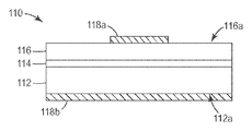
이제 도 1a를 참조하면, 도 1b 및 도 1c에 재현되어 있는 LED와 같은 반도체 전계발광 디바이스(110)의 개략 단면도이다. 디바이스(110)의 층 구성이 설명을 위해 단지 개략적으로 나타내어져 있다는 것과, 디바이스의 구성 요소가 꼭 축척대로 그려져 있는 것은 아니라는 것과, 부가의 요소가 포함될 수 있거나 예시된 요소가 원하는 바에 따라 생략되거나 수정될 수 있다는 것을 잘 알 것이다. 도시된 바와 같이, 디바이스(110)는 반도체 기층(112), 발광층(114), 및 전류 확산층(116)을 포함한다. 기층(112)은, 예를 들어, p-형 GaN 또는 기타 적당한 반도체 물질일 수 있거나 이를 포함할 수 있다. 발광층(114)은 p-형 클래딩층(cladding layer)과 n-형 클래딩층(도시 생략) 사이에 끼여 있는 활성층일 수 있거나 이를 포함할 수 있으며, 이들 각각은, 예를 들어, AlGaInN-기반 물질 또는 다른 적당한 반도체 물질을 포함할 수 있다. 전류 확산층(116)은, 예를 들어, Si 또는 기타 적당한 반도체 물질과 같은 n-형 도펀트가 어떤 농도로 도핑되어 있는 GaN-기반 물질과 같은 n-형 반도체일 수 있거나 이를 포함할 수 있다.Referring now to FIG. 1A, a schematic cross-sectional view of a
또한, 외부 전자 회로에 의해 공급되는 전기 구동 전류 또는 유사한 전기 신호가 디바이스에 인가되어 디바이스가 광을 방출할 수 있도록 각자의 외측 반도체층과 오옴 접촉하고 있는 제1 및 제2 전극(118a, 118b)이 제공되어 있다. 층(116)의 주 표면들 중 하나[예컨대, 외측 표면(116a)]로부터 우선적으로 광을 방출하기 위해, 디바이스(110)가, 도시된 바와 같이, 비대칭 설계로 제조될 수 있다. 이 때문에, 제1 전극(118a)은 표면(116a)의 일부분만을 덮도록 제조될 수 있는 반면, 제2 전극(118b)은 반대쪽 주 표면(112a)의 실질적으로 전부를 덮도록 제조될 수 있다. 제2 전극(118a)이 적어도 부분적으로 반사성이 있는 경우(예컨대, 금속성인 경우), 디바이스(110) 내에서 발생된 일부 광 - 그렇지 않았으면 주 표면(112a)을 통해 탈출하게 될 것임 - 이 디바이스의 측면 표면 또는 주 표면(116a)을 통해 탈출하도록 전극(118b)에 의해 반사될 수 있다. 물론, 개시된 실시 형태에서 사용될 수 있는 반도체 전계발광 디바이스가 광 방출의 전방향/역방향 특성에서 또는 전극의 배열에서 비대칭일 필요가 없다.The first and
도 1b 및 도 1c는 전기 신호가 전극에 인가될 때의 디바이스(110)의 거동을 정량적이고 개략적으로 나타낸 것이다. 도 1b에서, 제1 크기를 갖는 제1 신호가 인가된다. 도 1c에서, 제2 크기를 갖는 제2 신호가 인가된다. 신호 크기가 원하는 바에 따라 특징지워질 수 있지만, 대부분의 반도체 다이오드 디바이스의 I-V(전류-전압) 특성과 관련하여, 신호 크기를 전류로 나타내는 것이 대체로 논리적이다. 대안적으로, 신호 크기를 전위(전압)로 나타낼 수 있다. 어느 경우든지, 전극(118a)으로부터 디바이스(110)의 내부를 통해 다른 전극(118b)까지의 전류 분포가 제1 신호에 대해서는 화살표(120)로 나타내어져 있고(도 1b), 제2 신호에 대해서는 화살표(122)로 나타내어져 있다(도 1c).1B and 1C illustrate quantitatively and schematically the behavior of
각자의 신호가 동일한 디바이스(110)에 인가된다는 것을 상기하면, 화살표(122)의 패턴과 비교하여 화살표(120)의 패턴의 상이한 폭 또는 횡방향 치수로 예시된 전류 분포의 차이가 각자의 신호의 상이한 크기 및 "전류 집중" 현상의 결과이다. 도면으로부터 명백한 바와 같이, 전류 집중으로 인해 제1 신호(도 1b)와 비교하여 제2 신호(도 1c)의 전류 분포가 더 좁거나 더 집중되어 있다. 이 전류 집중 현상은 전형적으로 높은 전류 밀도에서 일어난다. 즉, 제2 신호는 전형적으로 제1 신호보다 더 큰 신호 크기(전류로 측정됨)를 가질 것이다. 디바이스(110)의 경우에, 전류 집중은 p-n 접합부가 높은 전류 레벨에서 감소된 전기 저항을 갖는 것의 결과일 수 있다. 감소된 저항은 전류가 전극(118a)으로부터 전극(118b)까지 보다 똑바른 경로로 흐르게 하는 경향이 있으며, 이는 도 1b의 전류 분포와 비교하여 전극(118a) 아래에 전류 "뭉침"(current bunching)을 야기한다.Recalling that the respective signals are applied to the
상이한 신호 크기에 대한 디바이스 내에서의 전류 분포의 변화는 또한 디바이스(110)에 의해 발생되는 광의 공간 분포에 영향을 미친다. 이러한 이유는 발광층(114)이, 전류가 발광층을 통해 흐르는 정도로만, 광을 발생할 것이기 때문이다. 전류 밀도가 낮은 발광층의 부분이, 한계 내에서, 전류 밀도가 높은 부분보다 적은 광을 발생할 것이다. [예컨대, 주 표면(116a)에 수직인 축을 따라 디바이스를 볼 때] 단위 체적당 또는 단위 투영 면적당 발생된 광의 차단값(cutoff value)을 지정함으로써, 발광층(114)의 고휘도 영역을 정의할 수 있다. 차단값은, 예를 들어, 기준 광 방출 레벨의 분율(fraction)일 수 있으며, 여기서 기준 레벨은 최대 광 방출이거나 전체 발광층에 걸친 공간적으로 평균된 광 발생일 수 있고, 이 분율은 기준 값의 ½, 1/10, 또는 1/e과 같이 원하는 바에 따라 선택될 수 있다. 이들 파라미터 중 어느 것을 선택하든 간에, 발광층의 고휘도 영역의 공간 범위를 특징지우는 일관성있는 방식을 제공하기 위해 얻어진 차단값을 사용할 수 있다. 고휘도 영역이 도 1b에서는 라벨 124로 그리고 도 1c에서는 라벨 126으로 표시되어 있다. 예상할 것인 바와 같이, 영역(124)은 영역(126)보다 더 큰 폭 또는 횡방향 치수를 가진다. 영역(124)과 비교하여 영역(126)을 생성하는 데 (전형적으로) 실질적으로 보다 큰 전류 레벨이 사용되는 것을 고려하면, 영역(124)이 영역(126)과 비교하여 크게 감소된 전체 광 방출 레벨을 가질 수 있더라도 이러할 수 있다.Changes in the current distribution within the device for different signal magnitudes also affect the spatial distribution of light generated by the
영역(124, 126)의 횡방향 치수 또는 기타 공간 범위의 차이로 인해 디바이스의 외측 표면(116a)으로부터 방출된 광의 공간 분포에서 대응하는 차이가 생긴다. 따라서, 표면(116a)으로부터 방출된 광의 보다 좁은 공간 분포를 야기하는 비교적 좁은 영역(126)과 비교하여, 비교적 넓은 영역(124)은 표면(116a)으로부터 방출된 광의 비교적 넓은 공간 분포를 야기한다. 달리 말하면, 제2 신호를 사용하여 표면(116a)으로부터 방출된 광의 공간 분포는 제1 신호에 대한 공간 분포보다 전극(118a) 쪽으로 더 집중되어 있다. 영역(124, 126)에서와 같이, 표면(116a)으로부터 방출된 광의 공간 분포는 상대적 용어로(예를 들어, 최대 또는 평균값의 분율 또는 퍼센트로서) 특징지워지거나 측정될 수 있다. 따라서, 제2 신호가 제1 신호보다 더 큰 크기를 갖는 것으로 가정할 때, 표면(116a)으로부터의 방출된 광의 그 각자의 공간 분포의 차이는 제2 신호에 대해 표면(116a)으로부터 방출된 광의 총량이 제1 신호에 대한 것보다 더 클 수 있다는 사실과 무관하다.Differences in the transverse dimensions or other spatial extents of
대체로, 전류 집중의 정도는 전류 확산층의 면 저항(sheet resistivity)에 의해 제어될 수 있다. 이러한 전류 집중 효과의 수학적 모델은 E. Fred Schubert의 Light-Emitting Diodes, 제2판(Cambridge University Press)의 제8장에서 찾아볼 수 있다.In general, the degree of current concentration can be controlled by the sheet resistivity of the current spreading layer. A mathematical model of this current concentration effect can be found in Chapter 8 of E. Fred Schubert's Light-Emitting Diodes, 2nd edition (Cambridge University Press).
지금까지, 전류 집중 현상 또는 그의 특정 측면, 및 전계발광 디바이스의 표면으로부터 방출된 광의 공간 분포에 대한 그의 효과에 대해 기술하였으며, 이제부터는 계속하여 이것이 인가된 전기 신호에 기초하여 색상(예컨대, 색 온도)을 변경하도록 광 출력(예컨대, 백색 광)이 만들어질 수 있는 조명 시스템을 제공하는 데 어떻게 사용될 수 있는지에 대해 기술할 것이다.So far, the current concentration phenomenon or a specific aspect thereof and its effect on the spatial distribution of light emitted from the surface of the electroluminescent device have been described and from now on it will continue to be based on the color (eg color temperature) based on the applied electrical signal. We will describe how the light output (eg, white light) can be used to provide an illumination system that can be made to change.
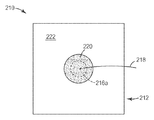
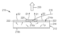
조명 시스템(210)이 도 2a에서는 개략 평면도로 도시되어 있고, 도 2b에서는 개략 단면도로 도시되어 있다. 이 시스템은 인가된 전기 신호에 응답하여 광을 방출하도록 구성된 전계발광 디바이스(212)를 포함한다. 전계발광 디바이스(212)는 제1 및 제2 전극(216a, 216b)이 그의 외측 표면에 부착되어 있는 본체(214)를 포함한다. 본체(214)가 개략적으로 그려져 있으며, 예를 들어, 반도체 LED에서 발견되는 것과 같은 반도체층(개별적으로 도시되지 않음)의 임의의 적당한 적층물을 포함할 수 있다. 본체는, 도시된 바와 같이, 개별 칩 또는 다이의 형태로, 또는 다이싱 이전의 전체 반도체 웨이퍼의 형태로 되어 있을 수 있다. 중요한 점은, 디바이스(212)가 전류 집중 현상을 나타내도록 또는 실질적으로 인가된 전기 신호의 크기의 함수로서 변하는 방출된 광의 공간 분포를 다른 방식으로 나타내도록, 본체(214)를 이루고 있는 층들이 설계되어 있다는 것이다. 전기 신호는, 물론, 전극(216a, 216b)에 인가되며, 여기서 외부 전기 구동기 또는 소스로부터 디바이스(212)로 신호를 전달하는 데 도움을 주기 위해 가는 와이어(218)가 와이어 본드를 통해 전극(216a)에 연결될 수 있다. 디바이스(212) 내에서 발생된 광은 비교적 작은 측면 표면을 통해 또는 제1 전극(216a)이 부착되어 있는 주 표면(214a)을 통해 탈출하거나 방출될 수 있다. 이러한 방출된 광은 펌프 광이라고 할 수 있으며, 도면에서 λp로 표시되어 있다. 펌프 광은, 예컨대, 350부터 500 ㎚까지의 범위에서 피크 파장을 갖는 청색, 보라색, 또는 자외광일 수 있거나 이들을 포함할 수 있지만, 펌프 광의 다른 스펙트럼 특성도 생각된다.
전계발광 디바이스의 설계의 결과로서, 표면(214a)으로부터 방출되는 펌프 광 λp의 공간 분포는 실질적으로 인가된 전기 신호의 크기의 함수로서 변한다. 예를 들어, 비교적 작은 크기를 갖는 제1 전기 신호는 표면(214a)으로부터 방출되는 공간 분포가 비교적 균일한 펌프 광을 제공할 수 있고, 보다 큰 크기를 갖는 제2 전기 신호는 표면(214a)으로부터 방출되는 공간 분포가 보다 작은 영역 - 전극(216a)을 둘러싸고 있는 고리 등 - 에 집중되어 있는 펌프 광을 제공할 수 있다.As a result of the design of the electroluminescent device, the spatial distribution of the pump light λ p emitted from the
전계발광 디바이스(212)에 부가하여, 시스템(210)은 또한 제1 및 제2 광 변경 물질(220, 222)을 포함한다. 이들 물질은 그에 부딪치는 펌프 광의 적어도 일부를 다른 파장의 광 성분으로 변환할 수 있다. 예를 들어, 제1 광 변경 물질(220)은 그에 부딪치는 펌프 광 λp의 적어도 일부를, 전형적으로 펌프 광의 파장보다 더 긴 다른 파장 λ1의 제1 광 성분으로 변환하는 인광체일 수 있거나 이를 포함할 수 있다. 제2 광 변경 물질은 그에 부딪치는 펌프 광 λp의 적어도 일부를, λ1와 상이하고 또한 전형적으로 펌프 광의 파장보다 더 긴 다른 파장 λ2의 제2 광 성분으로 변환하는 적어도 하나의 전위 우물을 갖는 RSC일 수 있거나 이를 포함할 수 있다. 광 변경 물질(220, 222) 중 하나 또는 둘다는 또한 부분적으로 펌프 광에 투명할 수 있으며, 따라서 제1 광 변경 물질(220)로부터 나가는 광은 파장 λ1의 제1 광 성분과 펌프 광 λp의 결합 또는 혼합을 포함할 수 있고, 및/또는 제2 광 변경 물질(222)로부터 나가는 광은 파장 λ2의 제2 광 성분과 펌프 광 λp의 결합 또는 혼합을 포함할 수 있다. 대안적으로, 이들 광 변경 물질(220, 222) 둘다는 실질적으로 펌프 광 λp에 불투명할 수 있다. 어느 경우든지, 제1 광 변경 물질(220)로부터 나가는 광은 적어도 파장 λ1의 제1 광 성분을 포함하고 또한 펌프 광도 포함할 수 있는 스펙트럼 S1에 의해 특징지워질 수 있는 반면, 제2 광 변경 물질(222)로부터 나가는 광은 적어도 파장 λ2의 제2 광 성분을 포함하고 또한 펌프 광도 포함할 수 있는 상이한 스펙트럼 S2에 의해 특징지워질 수 있다.In addition to the
자유 공간 전파에 의해서든 광 확산기, 렌즈, 거울 등과 같은 메커니즘을 통해서든, 스펙트럼 S1과 스펙트럼 S2에 의해 특징지워지는 광이 결합되어(선택적으로 다른 광 성분과 결합되어), 화살표(230)로 개략적으로 나타낸 조명 시스템(210)의 시스템 광 출력을 생성한다. 시스템 광 출력(230)은 따라서 얼마간의 제1 스펙트럼 S1의 광과 얼마간의 제2 스펙트럼 S2의 광을 포함한다. 달리 말하면, 시스템 광 출력(230)은 얼마간의 파장 λ1의 제1 광 성분과 얼마간의 파장 λ2의 제2 광 성분을 포함한다. 상이한 스펙트럼 S1, S2는 상이한 인지된 색상과 연관되어 있고, 이들의 결합(선택적으로 다른 광 성분과의 결합)은 시스템 광 출력(230)에 대한 또 다른 인지된 색상을 생성한다. 시스템 광 출력(230)의 인지된 색상(예컨대, 색 온도)은 따라서 시스템 광 출력(230)에 포함되는 제1 및 제2 광 성분의 상대적 양을 변경함으로써 조정되거나 변경될 수 있다.Whether by free-space propagation or through mechanisms such as light diffusers, lenses, mirrors, etc., the light characterized by spectra S1 and S2 is combined (optionally combined with other light components) and outlined by
이상에 기술된 전계발광 디바이스(212)의 전류 집중 특성을 고려하면, 제1 및 제2 광 변경 물질에 의해 제공되는 광의 상대적 양을 이와 같이 변경하는 것은, 제1 및 제2 광 변경 물질(220, 222)이 표면(214a)으로부터 방출되는 펌프 광의 공간 분포의 변화와 상승 작용을 하는 방식으로 공간적으로 분포되어 있기만 하다면, 단순히 인가된 전기 신호의 크기를 변경하는 것에 의해 달성될 수 있다. 예를 들어, 인가된 전기 신호의 변화로 인해 제2 부분에 비해 더 많은 펌프 광이 표면의 제1 부분으로부터 방출되는 경우, 그리고 제1 광 변경 물질이 제1 부분에 배치되어 있는 반면 제2 광 변경 물질이 제2 부분에 배치되어 있는 경우, 인가된 전기 신호의 변화는 시스템 광 출력(230)에서 제1 광 성분(또는 스펙트럼 S1의 광)을 상대적으로 더 많이 제공하고 제2 광 성분(또는 스펙트럼 S2의 광)을 상대적으로 더 적게 제공할 수 있으며, 따라서 시스템 광 출력의 인지된 색상을 변경할 수 있다.Given the current concentrating characteristics of the
도 2a 및 도 2b의 실시 형태에서, 제1 광 변경 물질(220)은 전극(220)에 근접하여 원 또는 효과적인 고리(effective annulus)의 형태로 배치되어 있다. 제2 광 변경 물질(222)은 표면(214a)의 나머지에[즉, 전극(220)으로부터 일정 거리 떨어져] 배치되어 있다. 광 변경 물질(220, 222)의 이러한 공간 배열은 전류 집중 현상으로부터 얻어지는 펌프 광의 공간 분포의 변화와 상승 작용을 한다. 낮은 전류 레벨에서, 비교적 균일한 분포의 펌프 광이 표면(214a)으로부터 방출되고, 이는 시스템 광 출력에서의 스펙트럼 S1의 광 대 스펙트럼 S2의 광의 초기 또는 기준 비율을 생성한다. 전류 집중이 방출된 펌프 광의 공간 분포를 전극(216a)을 둘러싸고 있는 고리와 같은 보다 작은 영역으로 한정하는 높은 전류에서, 시스템 광 출력(230)은 스펙트럼 S1의 광을 상대적으로 더 많이 포함하고 스펙트럼 S2의 광을 상대적으로 더 적게 포함할 것이며, 따라서 이러한 광 성분들의 상이한 비율 및 시스템 광 출력(230)의 상이한 인지된 색상을 야기한다. 인가된 전기 신호의 크기의 증가에 대한 시스템 광 출력의 색의 변화가 공칭 백색 광 출력의 색 온도의 증가에 대응하도록, 제1 및 제2 광 변경 물질이 필요에 따라 적절히 선택될 수 있다. 대안적으로, 정반대 효과를 생성하도록 광 변경 물질이 선택될 수 있고, 이 경우 인가된 전기 신호의 크기의 증가에 대한 시스템 광 출력의 색의 변화가 공칭 백색 광 출력의 색 온도의 감소에 대응한다.In the embodiment of FIGS. 2A and 2B, the first
도 2a 및 도 2b에 도시된 것에 대한 대안의 실시 형태에서, 제1 광 변경 물질(220)이 생략될 수 있거나, 제2 광 변경 물질(222)이 생략될 수 있으며, 따라서 단지 하나의 광 변경 물질이 조명 시스템에 포함되어 있다. 따라서, 예를 들어, 제1 광 변경 물질(220)이 생략되어 있는 경우, 스펙트럼 S1의 광은 전극(216a)을 둘러싸고 있는 표면(214a)의 환상 영역으로부터 방출되는 파장 λp의 펌프 광만을 포함할 수 있다. 대안적으로, 제2 광 변경 물질(222)이 생략되어 있는 경우, 스펙트럼 S2의 광은 이러한 환상 영역의 바깥쪽에 있는 표면(214a)의 부분으로부터 방출되는 파장 λp의 펌프 광만을 포함할 수 있다.In alternative embodiments to those shown in FIGS. 2A and 2B, the first
또 다른 대안의 실시 형태에서, 제3, 제4, 기타 광 변경 물질과 같은 부가의 광 변경 물질이 제공되고, 전류 집중 현상으로 인해 일어나는 펌프 광의 공간 분포의 변화와 상승 작용을 하는 패턴으로 다른 광 변경 물질과 함께 공간적으로 배열될 수 있으며, 따라서 시스템 광 출력의 색상이 인가된 전기 신호의 크기에 기초하여 변한다. 주목할 점은, 광 변경 물질의 설계에 따라, 주어진 광 변경 물질이 파장 λp의 펌프 광을, 하나의 피크 파장에서의 단지 하나의 피크(예컨대, 가우시안 또는 종-형상의 스펙트럼 분포를 가짐)에 의해 특징지워지는 광 성분으로, 또는 다수의 피크 파장에서의 다수의 피크에 의해 특징지워지는 광 성분으로 변환할 수 있다는 것이다. 예를 들어, RSC는 단지 하나의 전위 우물을 포함할 수 있거나, 동일하거나 유사한 설계의 다수의 전위 우물을 포함할 수 있으며, 따라서 변환된 광의 스펙트럼이 단지 하나의 피크에 의해 특징지워진다. 대안적으로, RSC는 실질적으로 상이한 설계의 다수의 전위 우물을 포함할 수 있고, 따라서 변환된 광의 스펙트럼이 복수의 피크에 의해 특징지워진다.In another alternative embodiment, additional light modifying materials such as third, fourth, and other light modifying materials are provided, and the other light in a synergistic pattern with the change in spatial distribution of the pump light resulting from the current concentration phenomenon. It can be arranged spatially with the modifying material, so that the color of the system light output changes based on the magnitude of the applied electrical signal. Note that, depending on the design of the light modifying material, a given light modifying material may pump pump light of wavelength λ p to only one peak (eg, Gaussian or species-shaped spectral distribution) at one peak wavelength. To light components characterized by, or to light components characterized by multiple peaks at multiple peak wavelengths. For example, the RSC may include only one potential well, or may include multiple potential wells of the same or similar design, such that the spectrum of the converted light is characterized by only one peak. Alternatively, the RSC may comprise a plurality of potential wells of substantially different designs, such that the spectrum of the converted light is characterized by a plurality of peaks.
기술 분야의 당업자라면 인지된 색상을 특성 파악하고 정량화하는 데 사용되는 도구 또는 표준 - 상세하게는, CIE[Commission International de l'Eclairage(International Commission on Lighting)]에 의해 발표된 공지의 1931 CIE 색도 다이어그램 - 을 잘 알 것이다. 광원 또는 물품의 색상(또는 "색도" 또는 "색도 좌표")이 CIE 1931 표준 표색계를 사용하여 CIE 색도 다이어그램 상의 하나 이상의 색도 좌표 (x,y)로 표현되는 지점 또는 영역에 의해 정확하게 측정되거나 지정될 수 있다.Tools or standards used by those skilled in the art to characterize and quantify perceived colors—in particular, the known 1931 CIE chromaticity diagram published by the Commission International de l'Eclairage (International Commission on Lighting). -You will know well. The color (or "chromatic" or "chromatic coordinate") of a light source or article may be accurately measured or specified by a point or area represented by one or more chromaticity coordinates (x, y) on a CIE chromaticity diagram using the CIE 1931 standard colorimetric system. Can be.
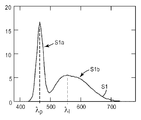
이러한 색도 다이어그램이 도 3에 도시되어 있다. 기술 분야의 당업자라면, 곡선(310)을 "플랑키안 궤적"(즉, 켈빈 온도로 측정되는 일정 범위의 온도 - 이 온도를 "색 온도" Tc라고 함 - 에 걸쳐 이상적인 흑체 광원의 색상)으로서 인식할 것이다.This chromaticity diagram is shown in FIG. 3. As one of ordinary skill in the art would appreciate,
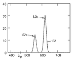
지점(312, 314)은, 각각, 도 2a 및 도 2b의 조명 시스템(210)의 일 실시 형태에 대한 스펙트럼 S1의 광 및 스펙트럼 S2의 광의 색 좌표를 나타낸다. 이들 지점의 스펙트럼이, 각각, 도 3a 및 도 3b에서 광 파장의 함수로서 표시되어 있다. 즉, 도 3a는 도 3에서의 지점(312)에 대응하는 스펙트럼 S1을 그래프로 나타낸 것이고, 도 3b는 도 3에서의 지점(314)에 대응하는 스펙트럼 S2를 그래프로 나타낸 것이다. 스펙트럼 S1은 2개의 주 성분: 제1 광 변경 물질(220)을 통해 투과되는 파장 λp의 펌프 광에 대응하는 비교적 좁은 스펙트럼 피크 S1a, 및 제1 광 변경 물질(예컨대, YAG:Ce 인광체)에 의해 생성되는 파장 λ1의 제1 광 성분에 대응하는 보다 넓은 스펙트럼 피크 S1b를 가진다. 스펙트럼 S2도 역시 2개의 주 성분: 비교적 좁은 제1 스펙트럼 피크 S2a 및 비교적 좁은 제2 스펙트럼 피크 S2b를 가진다. 이들 2개의 피크는 청색 펌프 광을 제1 피크 S2a의 광으로 변환할 수 있는 적어도 하나의 전위 우물 및 펌프 광을 제2 피크 S2b의 광으로 변환할 수 있는 적어도 다른 전위 우물을 가지는 청색-LED-펌핑된 RSC에 의해 생성될 수 있다. 주목할 점은, 스펙트럼 S2에서 펌프 파장 λp에 어떤 피크도 없는 것에 의해, 제2 광 변환 물질(즉, RSC)이, 이 특정의 실시 형태에서, 그에 입사하는 파장 λp의 모든 펌프 광을 흡수하거나 다른 방식으로 효과적으로 차단한다는 것이다.
도 3에서의 라인 세그먼트(316) - 그의 종점이 지점(312, 314)임 - 는 스펙트럼 S1의 광 및 스펙트럼 S2의 광의 선형 결합으로 이루어진 출력을 갖는 시스템에 대한 모든 가능한 조명 시스템 광 출력의 집합을 나타낸다. 따라서, 예를 들어, 스펙트럼 S1의 광과 스펙트럼 S2의 광을 똑같이 포함하는 광 출력을 갖는 조명 시스템은 라인 세그먼트(316)를 양분하는 지점에 의해 표현된다. 스펙트럼 S1의 광의 비율이 증가되면, 시스템 지점은 라인 세그먼트(316)를 따라 지점(312) 쪽으로 이동한다. 그 대신에 스펙트럼 S2의 광의 비율이 증가되면, 시스템 지점은 라인 세그먼트(316)를 따라 지점(314) 쪽으로 이동한다.
지점(312, 314)의 위치(색상)을 신중히 선택함으로써, 라인 세그먼트(316)는 플랑키안 궤적(310)의 일부분, 예를 들어, 2227℃(2500K)부터 4727℃(5000K)까지, 또는 2727℃(3000K)부터 4727℃(5000K)까지의 색 온도 범위에 걸친 궤적(310)의 부분에 아주 가깝게 될 수 있다. 이러한 경우에, 지점(312) 쪽으로 이동하는 라인 세그먼트(316) 상의 시스템 지점은 더 높은 색 온도 또는 "더 시원한"(청색 함유량이 더 많은) 백색 광원 쪽으로의 색상 변화에 대응한다. 그 대신에 시스템 지점이 지점(314) 쪽으로 이동하는 경우, 이는 더 낮은 색 온도 또는 "더 따뜻한"(적색 함유량이 더 많은) 광원 쪽으로의 색상 변화에 대응한다. 주목할 점은, 도 2a 및 도 2b의 조명 시스템(210)이, 도 3, 도 3a 및 도 3b와 관련하여 기술되는 광 변경 물질을 사용하여, 인가된 전기 신호의 크기가 증가함에 따라 낮은 색 온도로부터 높은 색 온도로[라인 세그먼트(316)를 따라 지점(312) 쪽으로] 천이하는 시스템 광 출력을 발생한다는 것이다.By carefully selecting the location (color) of the
스펙트럼 S1 및 S2의 특정의 형상은, 파장의 함수로서 표시될 때, CIE 색도 다이어그램 상에서의 그 각자의 지점(312, 314)의 위치를 결정할 뿐만 아니라, 얻어진 시스템 광의 "연색 지수"라고 하는 특성도 결정한다. "연색 지수"(CRI)는, 조명 시스템 설계자가 눈으로 직접 관찰함으로써 인지될 때의 시스템 광 출력의 외관 또는 색상 뿐만 아니라, 예를 들어, 시스템 광 출력을 사용하여 반사된 광에서 보이는 물체 또는 물품의 외관에도 관심을 가지는 경우, 조명 시스템 설계자에 중요할 수 있는 파라미터이다. 제1 및 제2 백색 광원이 CIE 색도 다이어그램 상에서 동일한 색 좌표를 가질 수 있더라도, 물체 또는 물품의 반사 스펙트럼에 따라, 제1 공칭 백색 광원에 의해 조명될 때의 그의 외관이 제2 공칭 백색 광원에 의해 조명될 때와 아주 상이할 수 있다. 이것은 CIE 색도 다이어그램 상에서의 특정의 색 좌표가 실질적으로 서로 상이할 수 있는 다수의 광 스펙트럼과 연관될 수 있다는 사실의 결과이다. 연색의 효과를 설명하는 통상의 예시가, 예를 들어, 사무실 형광등에 의한 조명과 비교하여, 또는 가스 방전 가로등에 의한 조명과 비교하여 햇빛으로 조명될 때 착색된 물체가 가지는 때때로 아주 상이한 외관이지만, 이들 조명 광원 모두가 직접 볼 때 공칭상 백색으로 보일 수 있다.The particular shape of the spectra S1 and S2, when expressed as a function of wavelength, not only determines the location of its
CIE 간행물 13.3-1995 "Method of Measuring and Specifying Colour Rendering Properties of Light Sources(광원의 연색 특성을 측정 및 지정하는 방법)"에 기술된 방법을 사용하여 주어진 광원의 연색 지수가 측정될 수 있다. 연색 지수는 일반적으로 최저 0부터 최고 100까지의 범위에 있으며, 높은 값이 일반적으로 바람직하다. 게다가, CIE 13.3-1995 간행물에 기초하여 주어진 광원을 나타내는 주어진 스펙트럼의 연색 지수를 계산할 수 있는 수치 기법 및 소프트웨어가 CIE로부터 이용가능하다.The color rendering index of a given light source can be measured using the method described in CIE Publication 13.3-1995 "Method of Measuring and Specifying Color Rendering Properties of Light Sources". The color rendering index generally ranges from as low as 0 to as high as 100 and high values are generally preferred. In addition, numerical techniques and software are available from CIE that can calculate the color rendering index of a given spectrum representing a given light source based on CIE 13.3-1995 publication.
이러한 소프트웨어가 도 3a 및 도 3b에 도시된 스펙트럼 S1 및 S2의 선형 결합으로 이루어진 시스템 광 출력의 연색 지수를 계산하는 데 사용될 때, 결과는 (스펙트럼 S1과 S2의 상이한 비율에 대응하는) 2227℃(2500K)부터 4727℃(5000K)까지의 색 온도 범위에 걸쳐 적어도 80의 연색 지수이다. 예시적인 실시 형태에서, 연색 지수는, 예를 들어, 2227℃(2500K)부터 4727℃(5000K)까지, 또는 2727℃(3000K)부터 4727℃(5000K)까지의 색 온도 범위에 걸쳐 적어도 60, 또는 적어도 70, 또는 적어도 80이다. 높은 연색 지수 값을 달성하기 위해, 시스템 광 출력을 이루고 있는 성분 스펙트럼(S1, S2) 각각이 적어도 2개의 개별 스펙트럼 피크(예컨대, 도 3a의 피크 S1a, S1b, 또는 도 3b의 피크 S2a, S2b) - 이들 피크가, 예를 들어, 적어도 10 ㎚만큼 서로 떨어져 있을 수 있음 - 에 의해 특징지워지도록 하는 것이 바람직하다. 이와 관련하여, 공동 출원된, 발명의 명칭이 "White Light Electroluminescent Devices With Adjustable Color Temperature(조정가능 색 온도를 갖는 백색 광 전계발광 디바이스)"인 미국 출원 제61/221,660호(대리인 사건 번호 65330US002)를 추가로 참조하며, 이 출원은 참조 문헌으로서 본 명세서에 포함된다.When such software is used to calculate the color rendering index of the system light output consisting of the linear combination of spectra S1 and S2 shown in FIGS. 3A and 3B, the result is 2227 ° C. (corresponding to the different ratios of spectra S1 and S2). A color rendering index of at least 80 over a color temperature range from 2500K) to 4727 ° C (5000K). In an exemplary embodiment, the color rendering index is at least 60, or, for example, over a color temperature range from 2227 ° C. (2500K) to 4727 ° C. (5000K), or from 2727 ° C. (3000K) to 4727 ° C. (5000K), or At least 70, or at least 80. In order to achieve a high color rendering index value, each of the component spectra S1, S2 constituting the system light output has at least two individual spectral peaks (e.g., peaks S1a, S1b of FIG. 3A, or peaks S2a, S2b of FIG. 3B). It is preferred that these peaks be characterized by being able to be separated from one another, for example by at least 10 nm. In this regard, U.S. Application No. 61 / 221,660 (Agent No. 65330US002), co-filed, entitled "White Light Electroluminescent Devices With Adjustable Color Temperature" For further reference, this application is incorporated herein by reference.
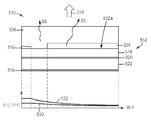
이제 도 4를 참조하면, 적어도 부분적으로 전류 집중의 결과로서, 인가된 전기 신호의 크기의 함수로서 상당한 색상 변화(color shift)를 나타낼 수 있는 다른 고체 조명 시스템(410)의 개략 단면도가 있다. 시스템(410)은 LED와 같은 2-단자 반도체 전계발광 디바이스(412)를 포함한다. 디바이스는 디바이스(412)의 베이스 전극에 전기적으로 결합된 제1 전도성 기둥(416)을 갖는 금속 헤더(414) 상에 탑재되어 있다. 헤더(414)로부터 전기적으로 절연되어 있는 제2 전도성 기둥(418)은 가는 와이어(420) 및 와이어 본드(422)를 통해 디바이스의 상부 전극에 전기적으로 결합되어 있다. 기둥(416, 418)은 시스템(410)의 2개의 단자를 형성하고, 디바이스에 전원을 공급하기 위해 이들 단자에 전기 신호가 인가된다. 디바이스의 상부 전극은 베이스 전극(base electrode)보다 작으며, 전계발광 디바이스(412)의 출력면(412a)의 한쪽 면으로부터 오프셋되어 있다.Referring now to FIG. 4, there is a schematic cross-sectional view of another solid
RSC(424)는 출력면(412a)의 제1 부분을 덮고 있으며, 이 제1 부분은, 도시된 바와 같이, 상부 전극으로부터 일정 간격 떨어지도록 공간적으로 배열될 수 있다. RSC(424)는 전계발광 디바이스 내에서 발생되는 방출된 광 또는 펌프 광을 스펙트럼 S3(예컨대, 호박색 광을 나타냄)을 가지는 제1 광 성분으로 변환하는 동작을 한다. 스펙트럼 S3는 뚜렷한 제1 및 제2 스펙트럼 피크(예컨대, 도 3b의 스펙트럼 S2와 동일하거나 유사함)를 포함할 수 있거나 본질적으로 이들로 이루어져 있을 수 있다. 스펙트럼 S3는 선택적으로 RSC(424)에 의해 투과된 잔류 펌프 광에 대응하는 뚜렷한 제3 스펙트럼 피크를 포함할 수 있거나, RSC(424)가 이러한 펌프 광을 실질적으로 차단하는 경우에 이러한 제3 스펙트럼 피크를 포함하지 않을 수 있다.
인광체(426)는 출력면(412a)의 제2 부분을 덮고 있고, 제2 부분은 제1 부분과 상이하며 상부 전극에 근접해 있는 영역 또는 구역을 포함한다. 인광체(426)는 펌프 광의 적어도 일부를 제2 광 성분(예컨대, 도 3a의 피크 S1b와 유사한 스펙트럼 피크를 가지는 황색 광)으로 변환하는 동작을 하며, 그 결과 스펙트럼 S4를 갖는 방출된 광이 얻어진다. 스펙트럼 S4를 갖는 광은 인광체(426)에 의해 발생되는 황색 광 뿐만 아니라, 인광체에 의해 투과된 잔류 펌프 광(예컨대, 도 3a의 스펙트럼 S1에 도시됨)도 포함할 수 있다. 스펙트럼 S3의 광과 스펙트럼 S4의 광이, 선택적으로, 다른 광 성분과 결합되어, 시스템 출력에 포함된 제1 및 제2 광 성분의 상대적 양 또는 비율에 의존하는 색 온도를 갖는 시스템 광 출력(428)(예컨대, 백색 광)을 제공한다.
인가된 전기 신호의 크기의 변화에 따른 시스템 출력의 색 온도의 변화는, 전계발광 디바이스(412)가 전류 집중을 나타내도록 함으로써, 즉 출력면(412a)을 통해 방출된 펌프 광의 공간 분포가 실질적으로 이러한 크기의 함수로서 변하도록 함으로써, 또한 방출된 광의 공간 분포에서의 이러한 변화가 RSC(424) 및 인광체(426)의 공간 분포와 상승 작용하게 하여 시스템 출력에 포함된 제1 및 제2 광 성분의 상대적 양 또는 비율이 대응하는 방식으로 변하도록 함으로써, 달성된다. 상세하게는, 전계발광 디바이스의 한쪽 면에 대해 상부 전극을 오프셋시킴으로써, RSC(424)의 반대쪽에서, 전류 집중 현상의 효과가 증진된다.The change in the color temperature of the system output with the change in the magnitude of the applied electrical signal causes the
도 5는 위치의 함수로서의 전류 밀도의 연관된 그래프와 함께, 시스템(410)과 유사한 조명 시스템(510)의 개략 단면도를 나타낸 것이다. 시스템(510)은 디바이스 내에서 발생된 펌프 광이 방출되는 출력면(512a)을 갖는 전계발광 디바이스(512)를 포함한다. 디바이스(512)는 또한 상부 전극(514), 베이스 전극(516), 및 성분 반도체층(518, 520, 522) - 이들 층은, 각각, 전류 확산층, p-n 접합층, 및 기판층일 수 있거나 이들을 포함할 수 있음 - 을 포함한다. 전류 확산층은, 예를 들어, AlGaInN 또는 다른 적당한 반도체 물질을 포함할 수 있고, p-n 접합부는, 예를 들어, GaInN 또는 다른 적당한 반도체 물질을 포함할 수 있으며, 기판층은, 예를 들어, 규소 또는 다른 적당한 반도체 물질을 포함할 수 있다. 도 4의 RSC(424)와 실질적으로 동일할 수 있는 제1 광 변경 물질(524)은 출력면(512a)의 제1 부분을 덮고 있으며 펌프 광의 제1 부분을 수광한다. 도 4의 인광체(426)와 실질적으로 동일할 수 있는 제2 광 변경 물질(526)은 출력면(512a)의 제2 부분을 덮고 있으며 펌프 광의 제2 부분을 수광한다. 스펙트럼 S5를 가지는 제1 광 변경 물질로부터 방출된 광 및 S5와 상이한 스펙트럼 S6을 갖는 제2 광 변경 물질로부터 방출된 광이 결합되어, 시스템 광 출력(528)을 형성한다.5 shows a schematic cross-sectional view of an
전극(514, 516)의 기하학적 구조 또는 레이아웃, 및 전극에 인가되는 전기 신호의 크기에 응답하여 변하는 전계발광 디바이스(512)의 하나 이상의 성분층의 하나 이상의 전기적 특성으로 인해, 상당한 전류 집중 현상이 관찰된다. 예를 들어, 높은 전류에서 제어된 양의 전류 집중을 제공하도록 n-GaN 층의 두께 및/또는 전도성이 설계될 수 있다. 이와 관련하여, p-n 접합층을 따른 횡방향 위치의 함수로서 p-n 접합층(520)을 통과하는 예상된 전류 밀도의 그래프가 동 도면에 제공되어 있다. 곡선(530)은 전극(514, 516)에 인가되는 제1 전류를 나타내고, 곡선(532)은 제1 전류보다 큰 제2 전류를 나타낸다. 이들 곡선은 제2 전류에 대한 p-n 접합층(520)의 비저항이 제1 전류에 대해서보다 낮은 것으로 가정한다. 양 곡선이 상부 전극(514)에 대응하는 위치에서 편평한 부분 또는 최대값을 나타내고 그 전극으로부터의 거리가 증가함에 따라 점차로 감소(taper off)하지만, 곡선(532)은 전극에 가까운 위치에서 더 많이 가중되거나 집중되어 있는 반면, 곡선(528)은 균일한 공간 분포에 더 가깝다. 이러한 전류 밀도의 차이로 인해 출력면(512a)으로부터 방출된 펌프 광의 공간 분포의 대응하는 차이가 생기며, 이는 제1 및 제2 광 변경 물질의 상이한 공간 분포와 결합하여, 시스템 광 출력(528)에서의 스펙트럼 S5의 광 및 스펙트럼 S6의 광의 상대적 양이 상이하게 되며 따라서 출력(528)의 색상 또는 색 온도의 변화를 야기한다.Due to the geometry or layout of the
제1 및 제2 광 변경 물질의 조성과, 출력면(512a) 상에서의 그 각자의 레이아웃 또는 공간 분포[예컨대, 전극(514)과 제1 광 변경 물질(524) 사이의 간극의 크기]는, 원하는 경우, 낮은 인가된 전류에서 특정의 색 온도[예컨대, 2227℃(2500K) 또는 2727℃(3000K)]를 나타내는 공칭 백색 광 출력을 갖고 높은 인가된 전류에서 증가하는 색 온도를 나타내는 시스템 광 출력을 제공하도록 선택될 수 있다. 전류의 증가에 따른 색 온도의 증가는, 예를 들어, 백열 광원과 연관된 색 온도의 변화에 가깝도록 설계될 수 있다.The composition of the first and second light modifying materials and their respective layout or spatial distribution on the
도 6 및 도 7은 색상 또는 색 온도가 인가된 전기 신호의 함수로서 변하는 시스템 광 출력을 제공할 수 있는 다른 조명 시스템의 개략 평면도를 나타낸 것이다. 간략함을 위해, 전계발광 디바이스의 설계의 상세가 도시되어 있지 않으며, 그와 관련해서는 이상의 설명을 참조하기 바란다. 그 대신에, 도 6 및 도 7은 상부 전극의 대안의 설계 및 원하는 색상 변화 효과를 생성하는 데 사용될 수 있는 제1 및 제2 광 변경 물질의 공간 분포를 나타내고 있다.6 and 7 show schematic plan views of other lighting systems that can provide system light output that changes color or color temperature as a function of an applied electrical signal. For the sake of simplicity, details of the design of the electroluminescent device are not shown, with reference to the above description. Instead, FIGS. 6 and 7 illustrate the spatial design of the first and second light modifying materials that can be used to produce an alternative design of the top electrode and the desired color change effect.
도 6에서, 조명 시스템(610)은, 도시된 바와 같이, 전계발광 디바이스의 출력면 상에 배치된 상부 전극(612)을 포함한다. 제1 광 변경 물질(614)은 공간적으로 전극(612)에 근접하여 배열 또는 배치되어 있다. 제2 광 변경 물질(616)은 공간적으로 전극(612)로부터 일정 간격 떨어져 배열 또는 배치되어 있다. 전류 집중으로 인해, 전기 신호의 크기가 증가됨에 따라 제2 광 변경 물질과 연관된 광에 비해 제1 광 변경 물질과 연관된 광이 더 많이 시스템 광 출력에 존재할 수 있다.In FIG. 6, the
도 7에서, 조명 시스템(710)은, 도시된 바와 같이, 전계발광 디바이스의 출력면 상에 배치된 상부 전극(712)을 포함한다. 제1 광 변경 물질(714)은 공간적으로 전극(712)에 근접하여 배열 또는 배치되어 있다. 제2 광 변경 물질(716)은 공간적으로 전극(712)로부터 일정 간격 떨어져 배열 또는 배치되어 있다. 출력면의 구역 또는 영역(718)은 어떤 광 변경 물질로도 덮여 있지 않으며, 따라서 전계발광 디바이스에서 발생된 펌프 광이 변경 없이 이 영역으로부터 방출된다. 전류 집중으로 인해, 전기 신호의 크기가 증가됨에 따라 제2 광 변경 물질과 연관된 광에 비해 제1 광 변경 물질과 연관된 광이 더 많이 시스템 광 출력에 존재할 수 있다.In FIG. 7, the
도 8은 RSC(808) 및 LED(802)를 겸비하고 있는 예시적인 디바이스(800)를 나타내고 있다. LED는 LED 기판(806) 상에 LED 반도체층(804) - 때때로 에피층(epilayer)이라고 함 - 의 적층물을 가진다. 층(804)은 p-형 및 n-형 접합부 층, 발광층(전형적으로 양자 우물을 포함함), 완충제 층, 및 상부판 층을 포함할 수 있다. 층(804)은 선택적인 접합층(816)을 통해 LED 기판(806)에 부착될 수 있다. LED는 상부면(812) 및 하부면을 가지고 있고, 상부면은 상부면이 편평한 경우와 비교하여 LED로부터의 광의 추출을 증가시키도록 텍스처링되어 있다. 도시된 바와 같이, 이들 상부면과 하부면 상에 전극(818, 820)이 제공될 수 있다. 이들 전극을 통해 적당한 전원에 연결될 때, LED는 청색 또는 자외선(UV) 광에 대응할 수 있는 제1 파장 λ1의 광을 방출한다. 이 LED 광의 일부는 RSC(808)에 들어가고 그곳에서 흡수된다.8 shows an
RSC(808)는 접합층(810)을 통해 LED의 상부면(812)에 부착되어 있다. RSC는 상부면 및 하부면(822, 824)을 가지며, 이 때 LED로부터의 펌프 광은 하부면(824)을 통해 들어간다. RSC는 또한 양자 우물 구조물(814) - 이 구조물의 일부분에서의 밴드 갭은 LED(802)에 의해 방출되는 펌프 광의 적어도 일부가 흡수되도록 선택되게 설계되어 있음- 을 포함한다. 펌프 광의 흡수에 의해 발생되는 전하 캐리어는 보다 작은 밴드 갭을 갖는 구조물의 다른 부분 - 즉, 양자 우물 층 - 내로 확산하고, 여기에서 캐리어는 재결합하여 보다 긴 파장의 광을 방출한다. 이것이 도 8에서 제2 파장 λ2의 재방출된 광 - 이는 RSC(808) 내로부터 나와서 RSC를 빠져나가 출력 광을 제공함 - 으로 나타내어져 있다.The
도 9는 RSC를 포함하는 예시적인 반도체층 적층물(910)을 나타내고 있다. 이 적층물은 분자 빔 에피택시(MBE)를 사용하여 인화인듐(InP) 웨이퍼 상에 성장되었다. GaInAs 버퍼 층이 II-VI족 성장을 위한 표면을 준비하기 위해 InP 기판 상에서 MBE에 의해 먼저 성장되었다. 이어서, RSC에 사용되는 II-VI족 에피택셜층을 성장시키기 위해 웨이퍼가 초고진공 이송 시스템을 통해 다른 MBE 챔버로 이동되었다. 막 성장된 RSC의 상세가 도 9에 도시되어 있고, 표 1에 요약되어 있다. 이 표는 RSC와 연관된 다른 층에 대한 두께, 물질 조성, 밴드 갭, 및 층 설명을 열거하고 있다. RSC는 8개의 CdZnSe 양자 우물(930) - 각각이 2.15 eV의 천이 에너지를 가짐 - 을 포함하였다. 각각의 양자 우물(930)은 LED에 의해 방출된 청색 광을 흡수할 수 있는 2.48 eV의 밴드 갭 에너지를 갖는 CdMgZnSe 흡수체 층(932) 사이에 끼여 있었다. RSC는 또한 다양한 윈도우 층, 완충제 층 및 경사층을 포함하였다.9 illustrates an example

이 RSC 디바이스 및 기타 RSC 디바이스에 대한 추가의 상세는 PCT 공개 WO 2009/048704(Kelley 등)에서 찾아볼 수 있다.Further details about this RSC device and other RSC devices can be found in PCT publication WO 2009/048704 (Kelley et al.).
도 3b에 도시된 스펙트럼과 유사한, 2개의 피크 파장을 포함하는 스펙트럼을 가지는 광을 동시에 방출할 수 있는 RSC를 포함하는 예시적인 반도체 적층물이 이하의 표 2에 나타내어져 있다. 이 적층물은 녹색 스펙트럼 피크를 생성하는 하나의 녹색-방출(555 ㎚) 양자 우물, 및 적색 스펙트럼 피크를 생성하는 하나의 적색-방출(620 ㎚) 양자 우물을 포함한다. 녹색 피크와 적색 피크의 상대적 세기는 원칙적으로 각자의 양자 우물과 연관되어 있는 흡수체 층의 두께에 의해 제어된다. 녹색-방출 양자 우물에 인접하여 비교적 얇은 흡수체 층을 사용함으로써, 보다 많은 펌프 광이 이들 층을 통과하고 적색-방출 양자 우물에 인접한 흡수체 층에서 흡수될 것이다. 이 결과, 녹색 광보다 더 많은 적색 광이 방출될 수 있다. 녹색 광 대 적색 광의 비가 또한 임의의 광-추출 특징부의 존재에 의해 얼마간 영향을 받을 수 있으며, 예컨대, 여기서 이러한 특징부는 시안 차단체의 외측 표면 내에 에칭되거나 그에 부착된다.An exemplary semiconductor stack including RSC capable of simultaneously emitting light having a spectrum comprising two peak wavelengths, similar to the spectrum shown in FIG. 3B, is shown in Table 2 below. This stack includes one green-emitting (555 nm) quantum well that produces a green spectral peak, and one red-emitting (620 nm) quantum well that produces a red spectral peak. The relative intensities of the green and red peaks are in principle controlled by the thickness of the absorber layer associated with the respective quantum wells. By using a relatively thin absorber layer adjacent to the green-emitting quantum wells, more pump light will pass through these layers and be absorbed in the absorber layer adjacent to the red-emitting quantum wells. As a result, more red light can be emitted than green light. The ratio of green light to red light can also be influenced in part by the presence of any light-extracting features, such as where such features are etched or attached to the outer surface of the cyan blocker.

기술 분야의 당업자라면 다양한 층에 대한 열거된 밴드 갭 에너지를 달성하기 위해 CdMgZnSe 합금의 조성을 어떻게 조정해야 하는지를 잘 알 것이다. 예를 들어, CdMgZnSe 합금의 밴드 갭 에너지는 주로 Mg 함유량에 의해 제어된다. 양자 우물의 방출 파장(또는 에너지)는 Cd/Zn 비 및 양자 우물의 정확한 두께 둘다에 의해 제어된다.Those skilled in the art will know how to adjust the composition of the CdMgZnSe alloy to achieve the listed band gap energy for the various layers. For example, the band gap energy of CdMgZnSe alloy is mainly controlled by the Mg content. The emission wavelength (or energy) of the quantum well is controlled by both the Cd / Zn ratio and the exact thickness of the quantum well.
달리 언급하지 않는 한, 본 명세서 및 특허청구범위에 사용되는 양, 특성의 측정치 등을 표현하는 모든 숫자는 "약"이라는 용어에 의해 수식되는 것으로 이해되어야 한다. 그에 따라, 달리 언급하지 않는 한, 명세서 및 특허청구범위에 기술되는 숫자 파라미터는 본 출원의 개시 내용을 이용하여 당업자가 달성하고자 하는 원하는 특성에 따라 다를 수 있는 근사치이다. 특허청구범위의 범주에 대한 등가물의 원칙의 적용을 제한하려고 시도함이 없이, 각각의 수치적 파라미터는 적어도 보고된 유효 숫자의 수의 관점에서 그리고 통상의 반올림 기법을 적용하여 해석되어야 한다. 본 발명의 넓은 범주를 기술하는 수치 범위 및 파라미터가 근사치임에도 불구하고, 임의의 수치 값이 본 명세서에 설명된 특정 예에 기술되는 한, 이들은 가능한 한 합리적으로 정확히 보고된다. 그러나, 임의의 수치 값은 시험 또는 측정 한계와 관련된 오차를 분명히 포함할 수 있다.Unless stated otherwise, all numbers expressing quantities, measurements of properties, and the like, used in this specification and claims are to be understood as being modified by the term "about." Accordingly, unless indicated to the contrary, the numerical parameters set forth in the specification and claims are approximations that may vary depending upon the desired properties sought by those skilled in the art using the disclosure of this application. Without attempting to limit the application of the principles of equivalents to the scope of the claims, each numerical parameter should be interpreted at least in terms of the number of reported significant digits and by applying the usual rounding techniques. Notwithstanding that the numerical ranges and parameters setting forth the broad scope of the invention are approximations, as far as any numerical value is set forth in the specific examples described herein, they are reported as reasonably accurate as possible. However, any numerical value may clearly include an error associated with a test or measurement limit.
본 발명의 다양한 수정 및 변경이 본 발명의 사상 및 범위를 벗어나지 않고 기술 분야의 당업자에게는 명백할 것이며, 본 발명이 본 명세서에 기술된 예시적인 실시 형태로 제한되지 않는다는 것을 잘 알 것이다. 예를 들어, 읽는 사람은, 달리 언급하지 않는 한, 하나의 개시된 실시 형태의 특징이 또한 모든 다른 개시된 실시 형태에도 적용될 수 있는 것으로 가정해야 한다. 또한, 본 명세서에서 언급된 모든 미국 특허, 특허 출원 공개, 및 기타 특허와 비특허 문서가, 이상의 개시 내용과 모순되지 않는 한, 참조 문헌으로서 포함된다는 것을 잘 알 것이다.Various modifications and variations of the present invention will be apparent to those skilled in the art without departing from the spirit and scope of the invention, and it will be appreciated that the invention is not limited to the exemplary embodiments described herein. For example, the reader should assume that features of one disclosed embodiment can also be applied to all other disclosed embodiments unless otherwise noted. It is also to be understood that all US patents, patent application publications, and other patents and non-patent documents mentioned herein are incorporated by reference, unless they contradict the above disclosure.
Claims (20)
인가된 전기 신호에 응답하여 광을 방출하도록 구성된 전계발광 디바이스, 및
제1 광 성분을 제공하기 위해 방출된 광의 제1 부분을 변경하도록 구성된 제1 광 변경 물질을 포함하고,
조명 시스템은 제1 광 성분을 방출된 광의 제2 부분과 연관된 적어도 제2 광 성분과 결합시켜 시스템 광 출력을 생성하며,
시스템 광 출력은 인가된 전기 신호에 기초하여 변하는 색 온도를 가지고,
색 온도의 변화가 적어도 부분적으로 전류 집중의 결과인 시스템.As a lighting system,
An electroluminescent device configured to emit light in response to an applied electrical signal, and
A first light modifying material configured to modify a first portion of emitted light to provide a first light component,
The illumination system combines the first light component with at least a second light component associated with the second portion of the emitted light to produce a system light output,
The system light output has a color temperature that changes based on the applied electrical signal,
A system in which the change in color temperature is at least partly a result of current concentration.
인가된 전류에 응답하여 출력면으로부터 광을 방출하도록 구성된 전계발광 디바이스 - 전계발광 디바이스는 출력면 상에서의 방출된 광의 공간 분포가 적어도 부분적으로 전류 집중의 결과로서 전류의 함수로서 변하는 것에 특징이 있음 -, 및
출력면의 제1 부분을 덮고 있고 방출된 광의 제1 부분을 제1 광 성분으로 변환하도록 구성된 제1 광 변환 물질을 포함하고,
제1 광 성분이 적어도 제2 광 성분과 결합하여 시스템 광 출력을 제공하며 - 제2 광 성분은 방출된 광의 제2 부분과 연관되어 있음 -,
출력면 상에서의 방출된 광의 공간 분포의 변화가 시스템 광 출력의 색의 변화를 야기하도록 제1 광 변환 물질이 공간적으로 분포되어 있는 것인 시스템.As a lighting system,
An electroluminescent device configured to emit light from an output surface in response to an applied current, wherein the electroluminescent device is characterized in that the spatial distribution of emitted light on the output surface changes at least in part as a function of current as a result of current concentration. , And
A first light converting material covering the first portion of the output surface and configured to convert the first portion of the emitted light into a first light component,
A first light component is combined with at least a second light component to provide system light output, the second light component being associated with a second portion of the emitted light;
And wherein the first light converting material is spatially distributed such that a change in spatial distribution of emitted light on the output surface causes a change in color of the system light output.
Applications Claiming Priority (2)
| Application Number | Priority Date | Filing Date | Title |
|---|---|---|---|
| US22166409P | 2009-06-30 | 2009-06-30 | |
| US61/221,664 | 2009-06-30 |
Publications (1)
| Publication Number | Publication Date |
|---|---|
| KR20120055540A true KR20120055540A (en) | 2012-05-31 |
Family
ID=42713858
Family Applications (1)
| Application Number | Title | Priority Date | Filing Date |
|---|---|---|---|
| KR1020127002064A KR20120055540A (en) | 2009-06-30 | 2010-06-25 | Electroluminescent devices with color adjustment based on current crowding |
Country Status (7)
| Country | Link |
|---|---|
| US (1) | US8304976B2 (en) |
| EP (1) | EP2449608A1 (en) |
| JP (1) | JP5728007B2 (en) |
| KR (1) | KR20120055540A (en) |
| CN (1) | CN102473816B (en) |
| TW (1) | TW201110803A (en) |
| WO (1) | WO2011008474A1 (en) |
Families Citing this family (7)
| Publication number | Priority date | Publication date | Assignee | Title |
|---|---|---|---|---|
| CN102460741A (en) | 2009-05-05 | 2012-05-16 | 3M创新有限公司 | Re-emitting semiconductor construction with enhanced extraction efficiency |
| US8994071B2 (en) | 2009-05-05 | 2015-03-31 | 3M Innovative Properties Company | Semiconductor devices grown on indium-containing substrates utilizing indium depletion mechanisms |
| WO2010129464A1 (en) | 2009-05-05 | 2010-11-11 | 3M Innovative Properties Company | Re-emitting semiconductor carrier devices for use with leds and methods of manufacture |
| WO2011008476A1 (en) | 2009-06-30 | 2011-01-20 | 3M Innovative Properties Company | Cadmium-free re-emitting semiconductor construction |
| EP2449856A1 (en) | 2009-06-30 | 2012-05-09 | 3M Innovative Properties Company | White light electroluminescent devices with adjustable color temperature |
| KR20150054937A (en) | 2012-09-13 | 2015-05-20 | 쓰리엠 이노베이티브 프로퍼티즈 컴파니 | Efficient lighting system with wide color range |
| TWI624821B (en) * | 2017-09-07 | 2018-05-21 | 錼創科技股份有限公司 | Micro light emitting diode display panel and driving method thereof |
Family Cites Families (65)
| Publication number | Priority date | Publication date | Assignee | Title |
|---|---|---|---|---|
| US3526801A (en) | 1964-08-07 | 1970-09-01 | Honeywell Inc | Radiation sensitive semiconductor device |
| JPH077847B2 (en) | 1984-12-17 | 1995-01-30 | 株式会社東芝 | Semiconductor light emitting element |
| US5048035A (en) | 1989-05-31 | 1991-09-10 | Kabushiki Kaisha Toshiba | Semiconductor light emitting device |
| JP2871477B2 (en) | 1994-09-22 | 1999-03-17 | 信越半導体株式会社 | Semiconductor light emitting device and method of manufacturing the same |
| JPH10500534A (en) | 1995-03-10 | 1998-01-13 | フィリップス エレクトロニクス ネムローゼ フェンノートシャップ | Illumination system for controlling color temperature of artificial light under the influence of daylight level |
| WO1998037259A1 (en) | 1997-02-19 | 1998-08-27 | Kirin Beer Kabushiki Kaisha | Method and apparatus for producing plastic container having carbon film coating |
| US6016038A (en) | 1997-08-26 | 2000-01-18 | Color Kinetics, Inc. | Multicolored LED lighting method and apparatus |
| US7014336B1 (en) | 1999-11-18 | 2006-03-21 | Color Kinetics Incorporated | Systems and methods for generating and modulating illumination conditions |
| JP3358556B2 (en) | 1998-09-09 | 2002-12-24 | 日本電気株式会社 | Semiconductor device and manufacturing method thereof |
| AU5463700A (en) | 1999-06-04 | 2000-12-28 | Trustees Of Boston University | Photon recycling semiconductor multi-wavelength light-emitting diodes |
| FR2801814B1 (en) | 1999-12-06 | 2002-04-19 | Cebal | METHOD FOR DEPOSITING A COATING ON THE INTERNAL SURFACE OF AEROSOL DISPENSING UNITS |
| US6902987B1 (en) | 2000-02-16 | 2005-06-07 | Ziptronix, Inc. | Method for low temperature bonding and bonded structure |
| TW497277B (en) | 2000-03-10 | 2002-08-01 | Toshiba Corp | Semiconductor light emitting device and method for manufacturing the same |
| US7202613B2 (en) | 2001-05-30 | 2007-04-10 | Color Kinetics Incorporated | Controlled lighting methods and apparatus |
| US6636003B2 (en) | 2000-09-06 | 2003-10-21 | Spectrum Kinetics | Apparatus and method for adjusting the color temperature of white semiconduct or light emitters |
| IL138471A0 (en) | 2000-09-14 | 2001-10-31 | Yissum Res Dev Co | Novel semiconductor materials and their uses |
| JP2004514285A (en) | 2000-11-17 | 2004-05-13 | エムコア・コーポレイション | Laser isolation die with tapered sidewalls to improve light extraction |
| US7358679B2 (en) | 2002-05-09 | 2008-04-15 | Philips Solid-State Lighting Solutions, Inc. | Dimmable LED-based MR16 lighting apparatus and methods |
| CA2427559A1 (en) | 2002-05-15 | 2003-11-15 | Sumitomo Electric Industries, Ltd. | White color light emitting device |
| US7591808B2 (en) | 2003-01-16 | 2009-09-22 | Femmepharma Holding Company, Inc. | Vaginal or rectal applicator |
| NO20041523L (en) | 2003-09-19 | 2005-03-21 | Sumitomo Electric Industries | Light emitting semiconductor element |
| DE10354936B4 (en) | 2003-09-30 | 2012-02-16 | Osram Opto Semiconductors Gmbh | Radiation-emitting semiconductor component |
| US7026653B2 (en) | 2004-01-27 | 2006-04-11 | Lumileds Lighting, U.S., Llc | Semiconductor light emitting devices including current spreading layers |
| TWI229465B (en) | 2004-03-02 | 2005-03-11 | Genesis Photonics Inc | Single chip white light component |
| TWI243489B (en) | 2004-04-14 | 2005-11-11 | Genesis Photonics Inc | Single chip light emitting diode with red, blue and green three wavelength light emitting spectra |
| US7361938B2 (en) | 2004-06-03 | 2008-04-22 | Philips Lumileds Lighting Company Llc | Luminescent ceramic for a light emitting device |
| US7553683B2 (en) | 2004-06-09 | 2009-06-30 | Philips Lumiled Lighting Co., Llc | Method of forming pre-fabricated wavelength converting elements for semiconductor light emitting devices |
| US7119377B2 (en) | 2004-06-18 | 2006-10-10 | 3M Innovative Properties Company | II-VI/III-V layered construction on InP substrate |
| US7126160B2 (en) | 2004-06-18 | 2006-10-24 | 3M Innovative Properties Company | II-VI/III-V layered construction on InP substrate |
| US7534633B2 (en) | 2004-07-02 | 2009-05-19 | Cree, Inc. | LED with substrate modifications for enhanced light extraction and method of making same |
| US7223998B2 (en) | 2004-09-10 | 2007-05-29 | The Regents Of The University Of California | White, single or multi-color light emitting diodes by recycling guided modes |
| AU2005322570A1 (en) | 2004-10-08 | 2006-07-06 | The Regents Of The University Of California | High efficiency light-emitting diodes |
| US7402831B2 (en) | 2004-12-09 | 2008-07-22 | 3M Innovative Properties Company | Adapting short-wavelength LED's for polychromatic, broadband, or “white” emission |
| TWI245440B (en) * | 2004-12-30 | 2005-12-11 | Ind Tech Res Inst | Light emitting diode |
| US7804100B2 (en) | 2005-03-14 | 2010-09-28 | Philips Lumileds Lighting Company, Llc | Polarization-reversed III-nitride light emitting device |
| US7417260B2 (en) | 2005-06-28 | 2008-08-26 | Dong-Sing Wuu | Multiple-chromatic light emitting device |
| JP4971672B2 (en) * | 2005-09-09 | 2012-07-11 | パナソニック株式会社 | Light emitting device |
| US20080272712A1 (en) * | 2005-09-19 | 2008-11-06 | Koninklijke Philips Electronics, N.V. | Variable Color Light Emitting Device and Method for Controlling the Same |
| US7285791B2 (en) | 2006-03-24 | 2007-10-23 | Goldeneye, Inc. | Wavelength conversion chip for use in solid-state lighting and method for making same |
| KR100875443B1 (en) | 2006-03-31 | 2008-12-23 | 서울반도체 주식회사 | Light emitting device |
| US20070284565A1 (en) | 2006-06-12 | 2007-12-13 | 3M Innovative Properties Company | Led device with re-emitting semiconductor construction and optical element |
| US7902542B2 (en) | 2006-06-14 | 2011-03-08 | 3M Innovative Properties Company | Adapted LED device with re-emitting semiconductor construction |
| US20080121911A1 (en) * | 2006-11-28 | 2008-05-29 | Cree, Inc. | Optical preforms for solid state light emitting dice, and methods and systems for fabricating and assembling same |
| JP2008159708A (en) * | 2006-12-21 | 2008-07-10 | Matsushita Electric Works Ltd | Light-emitting device |
| KR100829925B1 (en) | 2007-03-02 | 2008-05-16 | 세메스 주식회사 | Apparatus and method for processing substrate |
| CN101627482A (en) | 2007-03-08 | 2010-01-13 | 3M创新有限公司 | Array of luminescent elements |
| US7288902B1 (en) | 2007-03-12 | 2007-10-30 | Cirrus Logic, Inc. | Color variations in a dimmable lighting device with stable color temperature light sources |
| US7687816B2 (en) * | 2007-03-20 | 2010-03-30 | International Business Machines Corporation | Light emitting diode |
| US7759854B2 (en) | 2007-05-30 | 2010-07-20 | Global Oled Technology Llc | Lamp with adjustable color |
| US10505083B2 (en) * | 2007-07-11 | 2019-12-10 | Cree, Inc. | Coating method utilizing phosphor containment structure and devices fabricated using same |
| WO2009036579A1 (en) | 2007-09-21 | 2009-03-26 | Hoffmann Neopac Ag | Apparatus for plasma supported coating of the inner surface of tube-like packaging containers made of plastics with the assistance of a non-thermal reactive ambient pressure beam plasma |
| WO2009048704A2 (en) | 2007-10-08 | 2009-04-16 | 3M Innovative Properties Company | Light emitting diode with bonded semiconductor wavelength converter |
| CN101836297A (en) | 2007-10-26 | 2010-09-15 | 科锐Led照明科技公司 | Illumination device having one or more lumiphors, and methods of fabricating same |
| JP2011523212A (en) | 2008-06-05 | 2011-08-04 | スリーエム イノベイティブ プロパティズ カンパニー | Light emitting diode with semiconductor wavelength converter bonded |
| US9053959B2 (en) | 2008-06-26 | 2015-06-09 | 3M Innovative Properties Company | Semiconductor light converting construction |
| EP2308104A4 (en) | 2008-06-26 | 2014-04-30 | 3M Innovative Properties Co | Semiconductor light converting construction |
| WO2010019594A2 (en) | 2008-08-14 | 2010-02-18 | 3M Innovative Properties Company | Projection system with imaging light source module |
| JP2012502473A (en) | 2008-09-04 | 2012-01-26 | スリーエム イノベイティブ プロパティズ カンパニー | II-VI multiple quantum well vertical cavity surface emitting laser on a heat sink optically pumped by a gallium nitride laser diode |
| WO2010028146A2 (en) | 2008-09-08 | 2010-03-11 | 3M Innovative Properties Company | Electrically pixelated luminescent device |
| US8619620B2 (en) | 2008-09-16 | 2013-12-31 | Qualcomm Incorporated | Methods and systems for transmission mode selection in a multi channel communication system |
| JP2012514329A (en) | 2008-12-24 | 2012-06-21 | スリーエム イノベイティブ プロパティズ カンパニー | Light generating device with wavelength converter on both sides |
| CN102460741A (en) | 2009-05-05 | 2012-05-16 | 3M创新有限公司 | Re-emitting semiconductor construction with enhanced extraction efficiency |
| WO2011008476A1 (en) | 2009-06-30 | 2011-01-20 | 3M Innovative Properties Company | Cadmium-free re-emitting semiconductor construction |
| US8994071B2 (en) | 2009-05-05 | 2015-03-31 | 3M Innovative Properties Company | Semiconductor devices grown on indium-containing substrates utilizing indium depletion mechanisms |
| EP2449856A1 (en) | 2009-06-30 | 2012-05-09 | 3M Innovative Properties Company | White light electroluminescent devices with adjustable color temperature |
-
2010
- 2010-06-25 WO PCT/US2010/040009 patent/WO2011008474A1/en active Application Filing
- 2010-06-25 KR KR1020127002064A patent/KR20120055540A/en not_active Application Discontinuation
- 2010-06-25 CN CN201080029540.2A patent/CN102473816B/en not_active Expired - Fee Related
- 2010-06-25 US US13/379,933 patent/US8304976B2/en not_active Expired - Fee Related
- 2010-06-25 JP JP2012517773A patent/JP5728007B2/en not_active Expired - Fee Related
- 2010-06-25 EP EP10729750A patent/EP2449608A1/en not_active Withdrawn
- 2010-06-29 TW TW099121300A patent/TW201110803A/en unknown
Also Published As
| Publication number | Publication date |
|---|---|
| CN102473816A (en) | 2012-05-23 |
| TW201110803A (en) | 2011-03-16 |
| WO2011008474A1 (en) | 2011-01-20 |
| JP5728007B2 (en) | 2015-06-03 |
| JP2012532452A (en) | 2012-12-13 |
| CN102473816B (en) | 2015-03-11 |
| US20120091882A1 (en) | 2012-04-19 |
| EP2449608A1 (en) | 2012-05-09 |
| US8304976B2 (en) | 2012-11-06 |
Similar Documents
| Publication | Publication Date | Title |
|---|---|---|
| US8629611B2 (en) | White light electroluminescent devices with adjustable color temperature | |
| US10546843B2 (en) | White light emitting devices having high luminous efficiency and improved color rendering that include pass-through violet emissions | |
| US10074781B2 (en) | Semiconductor light emitting devices including multiple red phosphors that exhibit good color rendering properties with increased brightness | |
| KR100347126B1 (en) | White color LED and Neutral tint LED | |
| US10541353B2 (en) | Light emitting devices including narrowband converters for outdoor lighting applications | |
| US20140167601A1 (en) | Enhanced Luminous Flux Semiconductor Light Emitting Devices Including Red Phosphors that Exhibit Good Color Rendering Properties and Related Red Phosphors | |
| US9219202B2 (en) | Semiconductor light emitting devices including red phosphors that exhibit good color rendering properties and related red phosphors | |
| US8178888B2 (en) | Semiconductor light emitting devices with high color rendering | |
| US8304976B2 (en) | Electroluminescent devices with color adjustment based on current crowding | |
| KR20160019622A (en) | Semiconductor light emitting device and semiconductor light emitting device package | |
| CA2583504A1 (en) | High efficiency light-emitting diodes | |
| TW201411877A (en) | Photonic devices, light-emitting devices and methods of fabricating the light-emitting devices | |
| TWI597862B (en) | A photoelectronic semiconductor device with barrier layer | |
| US20120313119A1 (en) | Three dimensional light-emitting-diode (led) stack and method of manufacturing the same | |
| JP2000150961A (en) | Led element with light emitting substrate | |
| KR20200009847A (en) | Semiconductor device and light emitting device package having thereof | |
| US9054278B2 (en) | Lighting apparatuses and driving methods regarding to light-emitting diodes | |
| TWI639252B (en) | A photoelectronic semiconductor device with barrier layer | |
| US9905735B1 (en) | High brightness, low-cri semiconductor light emitting devices including narrow-spectrum luminescent materials | |
| KR101723540B1 (en) | Light emitting device and light emitting device package having the same | |
| US20240162391A1 (en) | Lumiphoric material arrangements for cover structures of light-emitting diode packages | |
| KR100588209B1 (en) | White light emitting device and method for fabricating the same | |
| Marioli | Study of the reliability of power LEDs for color mixing applications | |
| KR20000012012A (en) | luminescent substrate LED device | |
| US20140014987A1 (en) | Methods and apparatuses for shifting chromaticity of light |
Legal Events
| Date | Code | Title | Description |
|---|---|---|---|
| WITN | Application deemed withdrawn, e.g. because no request for examination was filed or no examination fee was paid |