KR20110039260A - Non-volatile memory arrays comprising rail stacks with a shared diode component portion for diodes of electrically isolated pillars - Google Patents
Non-volatile memory arrays comprising rail stacks with a shared diode component portion for diodes of electrically isolated pillars Download PDFInfo
- Publication number
- KR20110039260A KR20110039260A KR1020117000959A KR20117000959A KR20110039260A KR 20110039260 A KR20110039260 A KR 20110039260A KR 1020117000959 A KR1020117000959 A KR 1020117000959A KR 20117000959 A KR20117000959 A KR 20117000959A KR 20110039260 A KR20110039260 A KR 20110039260A
- Authority
- KR
- South Korea
- Prior art keywords
- diode element
- layer
- polysilicon layer
- diode
- conductor
- Prior art date
Links
- 238000003491 array Methods 0.000 title description 3
- 239000004020 conductor Substances 0.000 claims abstract description 97
- 230000008859 change Effects 0.000 claims abstract description 43
- 238000004519 manufacturing process Methods 0.000 claims abstract description 15
- 238000000034 method Methods 0.000 claims description 50
- 229910021420 polycrystalline silicon Inorganic materials 0.000 claims description 30
- 229910052710 silicon Inorganic materials 0.000 claims description 30
- 239000010703 silicon Substances 0.000 claims description 30
- 229920005591 polysilicon Polymers 0.000 claims description 29
- XUIMIQQOPSSXEZ-UHFFFAOYSA-N Silicon Chemical group [Si] XUIMIQQOPSSXEZ-UHFFFAOYSA-N 0.000 claims description 28
- 239000000758 substrate Substances 0.000 claims description 27
- 238000005530 etching Methods 0.000 claims description 25
- 239000004065 semiconductor Substances 0.000 claims description 9
- 238000000059 patterning Methods 0.000 claims description 3
- 238000009740 moulding (composite fabrication) Methods 0.000 claims 1
- 239000010410 layer Substances 0.000 description 144
- 239000000463 material Substances 0.000 description 39
- 230000008569 process Effects 0.000 description 31
- 239000012790 adhesive layer Substances 0.000 description 16
- 229920002120 photoresistant polymer Polymers 0.000 description 10
- 239000003989 dielectric material Substances 0.000 description 9
- VYPSYNLAJGMNEJ-UHFFFAOYSA-N Silicium dioxide Chemical compound O=[Si]=O VYPSYNLAJGMNEJ-UHFFFAOYSA-N 0.000 description 8
- 230000005684 electric field Effects 0.000 description 7
- 238000005229 chemical vapour deposition Methods 0.000 description 6
- 229910017052 cobalt Inorganic materials 0.000 description 6
- 239000010941 cobalt Substances 0.000 description 6
- GUTLYIVDDKVIGB-UHFFFAOYSA-N cobalt atom Chemical compound [Co] GUTLYIVDDKVIGB-UHFFFAOYSA-N 0.000 description 6
- AIOWANYIHSOXQY-UHFFFAOYSA-N cobalt silicon Chemical compound [Si].[Co] AIOWANYIHSOXQY-UHFFFAOYSA-N 0.000 description 5
- 229910052721 tungsten Inorganic materials 0.000 description 5
- 239000010937 tungsten Substances 0.000 description 5
- 230000015572 biosynthetic process Effects 0.000 description 4
- 230000007423 decrease Effects 0.000 description 4
- 238000009792 diffusion process Methods 0.000 description 4
- 238000005240 physical vapour deposition Methods 0.000 description 4
- 239000000126 substance Substances 0.000 description 4
- WFKWXMTUELFFGS-UHFFFAOYSA-N tungsten Chemical compound [W] WFKWXMTUELFFGS-UHFFFAOYSA-N 0.000 description 4
- 229910052581 Si3N4 Inorganic materials 0.000 description 3
- 150000001875 compounds Chemical class 0.000 description 3
- 238000000151 deposition Methods 0.000 description 3
- 230000003446 memory effect Effects 0.000 description 3
- 239000000377 silicon dioxide Substances 0.000 description 3
- 235000012239 silicon dioxide Nutrition 0.000 description 3
- HQVNEWCFYHHQES-UHFFFAOYSA-N silicon nitride Chemical compound N12[Si]34N5[Si]62N3[Si]51N64 HQVNEWCFYHHQES-UHFFFAOYSA-N 0.000 description 3
- 238000003860 storage Methods 0.000 description 3
- 229910000314 transition metal oxide Inorganic materials 0.000 description 3
- 238000000137 annealing Methods 0.000 description 2
- 238000000231 atomic layer deposition Methods 0.000 description 2
- 238000013500 data storage Methods 0.000 description 2
- 238000010586 diagram Methods 0.000 description 2
- 239000002019 doping agent Substances 0.000 description 2
- 239000012777 electrically insulating material Substances 0.000 description 2
- 230000006870 function Effects 0.000 description 2
- 238000002347 injection Methods 0.000 description 2
- 239000007924 injection Substances 0.000 description 2
- 239000011810 insulating material Substances 0.000 description 2
- 229910052751 metal Inorganic materials 0.000 description 2
- 239000002184 metal Substances 0.000 description 2
- 238000001465 metallisation Methods 0.000 description 2
- 230000004048 modification Effects 0.000 description 2
- 238000012986 modification Methods 0.000 description 2
- ORQBXQOJMQIAOY-UHFFFAOYSA-N nobelium Chemical compound [No] ORQBXQOJMQIAOY-UHFFFAOYSA-N 0.000 description 2
- 238000000206 photolithography Methods 0.000 description 2
- 229910052814 silicon oxide Inorganic materials 0.000 description 2
- -1 tungsten nitride Chemical class 0.000 description 2
- 238000001039 wet etching Methods 0.000 description 2
- OKTJSMMVPCPJKN-UHFFFAOYSA-N Carbon Chemical compound [C] OKTJSMMVPCPJKN-UHFFFAOYSA-N 0.000 description 1
- RYGMFSIKBFXOCR-UHFFFAOYSA-N Copper Chemical compound [Cu] RYGMFSIKBFXOCR-UHFFFAOYSA-N 0.000 description 1
- ATJFFYVFTNAWJD-UHFFFAOYSA-N Tin Chemical group [Sn] ATJFFYVFTNAWJD-UHFFFAOYSA-N 0.000 description 1
- RTAQQCXQSZGOHL-UHFFFAOYSA-N Titanium Chemical compound [Ti] RTAQQCXQSZGOHL-UHFFFAOYSA-N 0.000 description 1
- NRTOMJZYCJJWKI-UHFFFAOYSA-N Titanium nitride Chemical compound [Ti]#N NRTOMJZYCJJWKI-UHFFFAOYSA-N 0.000 description 1
- 230000002411 adverse Effects 0.000 description 1
- 229910045601 alloy Inorganic materials 0.000 description 1
- 239000000956 alloy Substances 0.000 description 1
- 238000004380 ashing Methods 0.000 description 1
- QVGXLLKOCUKJST-UHFFFAOYSA-N atomic oxygen Chemical compound [O] QVGXLLKOCUKJST-UHFFFAOYSA-N 0.000 description 1
- 230000004888 barrier function Effects 0.000 description 1
- 230000006399 behavior Effects 0.000 description 1
- 229910052799 carbon Inorganic materials 0.000 description 1
- 239000005387 chalcogenide glass Substances 0.000 description 1
- 238000011109 contamination Methods 0.000 description 1
- 229910052802 copper Inorganic materials 0.000 description 1
- 239000010949 copper Substances 0.000 description 1
- 230000001351 cycling effect Effects 0.000 description 1
- 230000007547 defect Effects 0.000 description 1
- 230000008021 deposition Effects 0.000 description 1
- 230000000694 effects Effects 0.000 description 1
- 230000001747 exhibiting effect Effects 0.000 description 1
- 239000007789 gas Substances 0.000 description 1
- 238000007654 immersion Methods 0.000 description 1
- 238000011065 in-situ storage Methods 0.000 description 1
- 230000006698 induction Effects 0.000 description 1
- 239000011229 interlayer Substances 0.000 description 1
- 238000005468 ion implantation Methods 0.000 description 1
- 229910021421 monocrystalline silicon Inorganic materials 0.000 description 1
- 230000007935 neutral effect Effects 0.000 description 1
- 239000011368 organic material Substances 0.000 description 1
- 229910052760 oxygen Inorganic materials 0.000 description 1
- 239000001301 oxygen Substances 0.000 description 1
- 238000005498 polishing Methods 0.000 description 1
- 229920006254 polymer film Polymers 0.000 description 1
- 239000002210 silicon-based material Substances 0.000 description 1
- 239000007787 solid Substances 0.000 description 1
- 125000006850 spacer group Chemical group 0.000 description 1
- 229910052715 tantalum Inorganic materials 0.000 description 1
- GUVRBAGPIYLISA-UHFFFAOYSA-N tantalum atom Chemical compound [Ta] GUVRBAGPIYLISA-UHFFFAOYSA-N 0.000 description 1
- MZLGASXMSKOWSE-UHFFFAOYSA-N tantalum nitride Chemical compound [Ta]#N MZLGASXMSKOWSE-UHFFFAOYSA-N 0.000 description 1
- 229910052719 titanium Inorganic materials 0.000 description 1
- 239000010936 titanium Substances 0.000 description 1
- MAKDTFFYCIMFQP-UHFFFAOYSA-N titanium tungsten Chemical compound [Ti].[W] MAKDTFFYCIMFQP-UHFFFAOYSA-N 0.000 description 1
- 230000007704 transition Effects 0.000 description 1
Images


Classifications
-
- H—ELECTRICITY
- H01—ELECTRIC ELEMENTS
- H01L—SEMICONDUCTOR DEVICES NOT COVERED BY CLASS H10
- H01L27/00—Devices consisting of a plurality of semiconductor or other solid-state components formed in or on a common substrate
- H01L27/02—Devices consisting of a plurality of semiconductor or other solid-state components formed in or on a common substrate including semiconductor components specially adapted for rectifying, oscillating, amplifying or switching and having potential barriers; including integrated passive circuit elements having potential barriers
- H01L27/04—Devices consisting of a plurality of semiconductor or other solid-state components formed in or on a common substrate including semiconductor components specially adapted for rectifying, oscillating, amplifying or switching and having potential barriers; including integrated passive circuit elements having potential barriers the substrate being a semiconductor body
- H01L27/10—Devices consisting of a plurality of semiconductor or other solid-state components formed in or on a common substrate including semiconductor components specially adapted for rectifying, oscillating, amplifying or switching and having potential barriers; including integrated passive circuit elements having potential barriers the substrate being a semiconductor body including a plurality of individual components in a repetitive configuration
- H01L27/102—Devices consisting of a plurality of semiconductor or other solid-state components formed in or on a common substrate including semiconductor components specially adapted for rectifying, oscillating, amplifying or switching and having potential barriers; including integrated passive circuit elements having potential barriers the substrate being a semiconductor body including a plurality of individual components in a repetitive configuration including bipolar components
- H01L27/1021—Devices consisting of a plurality of semiconductor or other solid-state components formed in or on a common substrate including semiconductor components specially adapted for rectifying, oscillating, amplifying or switching and having potential barriers; including integrated passive circuit elements having potential barriers the substrate being a semiconductor body including a plurality of individual components in a repetitive configuration including bipolar components including diodes only
-
- H—ELECTRICITY
- H10—SEMICONDUCTOR DEVICES; ELECTRIC SOLID-STATE DEVICES NOT OTHERWISE PROVIDED FOR
- H10B—ELECTRONIC MEMORY DEVICES
- H10B63/00—Resistance change memory devices, e.g. resistive RAM [ReRAM] devices
- H10B63/20—Resistance change memory devices, e.g. resistive RAM [ReRAM] devices comprising selection components having two electrodes, e.g. diodes
-
- H—ELECTRICITY
- H10—SEMICONDUCTOR DEVICES; ELECTRIC SOLID-STATE DEVICES NOT OTHERWISE PROVIDED FOR
- H10B—ELECTRONIC MEMORY DEVICES
- H10B63/00—Resistance change memory devices, e.g. resistive RAM [ReRAM] devices
- H10B63/80—Arrangements comprising multiple bistable or multi-stable switching components of the same type on a plane parallel to the substrate, e.g. cross-point arrays
Landscapes
- Engineering & Computer Science (AREA)
- Power Engineering (AREA)
- Physics & Mathematics (AREA)
- Condensed Matter Physics & Semiconductors (AREA)
- General Physics & Mathematics (AREA)
- Computer Hardware Design (AREA)
- Microelectronics & Electronic Packaging (AREA)
- Semiconductor Memories (AREA)
Abstract
전도체들 사이에서 수직적으로 배향된 다이오드 구조들을 포함하는 집적회로와 이를 제조하는 방법이 제공된다. 수동 소자 메모리 셀들과 같은 2 단자 디바이스들은, 안티퓨즈 및/또는 상태 변화 소자와 직렬인 다이오드 스티어링 소자를 포함할 수 있다. 상기 디바이스들은 전도체들의 상부 세트 및 하부 세트의 교차점에서 필라 구조를 이용하여 형성된다. 각 필라에 대해 다이오드의 일부를 상기 전도체들 중 하나를 구비한 레일 스택 내에 형성함으로써, 필라 구조의 높이가 감소된다. 일실시예에서 다이오드는 제 1 도전형의 제 1 다이오드 요소와 제 2 도전형의 제 2 다이오드 요소를 포함할 수 있다. 상기 다이오드 요소들 중 하나의 일부는 제 1 부분 및 제 2 부분으로 나뉘어지는바, 상기 부분들 중 하나는 레일 스택 내에 형성되며, 이는 레일 스택에서 필라들을 이용하여 형성된 다른 다이오드들과 공유된다. An integrated circuit comprising diode structures oriented vertically between conductors and a method of manufacturing the same are provided. Two-terminal devices, such as passive element memory cells, may include a diode steering element in series with the antifuse and / or state change element. The devices are formed using a pillar structure at the intersection of the upper and lower sets of conductors. By forming a portion of the diode for each pillar in a rail stack with one of the conductors, the height of the pillar structure is reduced. In one embodiment, the diode may comprise a first diode element of a first conductivity type and a second diode element of a second conductivity type. A portion of one of the diode elements is divided into a first portion and a second portion, wherein one of the portions is formed in the rail stack, which is shared with other diodes formed using pillars in the rail stack.
Description
본 발명에 따른 실시예들은 비휘발성 메모리 셀 어레이를 포함하는 집적회로에 관한 것이며 좀더 상세하게는 수동(passive) 소자 메모리 셀들을 포함하는 어레이에 관한 것이다. Embodiments in accordance with the present invention relate to an integrated circuit comprising a nonvolatile memory cell array and, more particularly, to an array comprising passive device memory cells.
가령, 저항 또는 위상 변화와 같은 상태 변화의 검출가능한 레벨을 갖는 물질들이, 다양한 유형의 비휘발성 반도체 기반의 메모리 디바이스를 형성하는데 이용되고 있다. 예를 들어, 메모리 셀의 저저항의 초기 물리적 상태를 제 1 논리 상태(가령, 논리 "0")에 할당하고, 그리고 메모리 셀의 고저항의 물리적 상태를 제 2 논리 상태(가령, 논리 "1")에 할당함으로써, 간단한 안티퓨즈(antifuse)들이 원타임 필드-프로그램가능(OTP) 메모리 어레이에서 이진 데이터 저장를 위해 이용된다. 몇몇 물질들은 그들의 저항을 초기 저항쪽으로 스위치 백할 수 있다. 이러한 유형의 물질들은 재기록가능한 메모리 셀을 형성하는데 이용될 수 있다. 물질의 검출가능한 저항의 다중 레벨은 또한, 다중 상태 디바이스를 형성하는데 이용될 수 있는바, 이는 재기록되거나 혹은 재기록될 수 없다. Materials with detectable levels of state change, such as, for example, resistance or phase changes, are used to form various types of nonvolatile semiconductor based memory devices. For example, assign an initial physical state of the low resistance of the memory cell to a first logic state (eg, logic "0"), and assign a physical state of the high resistance of the memory cell to a second logic state (eg, logic "1"). By assigning to "), simple antifuses are used for binary data storage in a one-time field-programmable (OTP) memory array. Some materials can switch back their resistance towards the initial resistance. Materials of this type can be used to form rewritable memory cells. Multiple levels of detectable resistance of a substance may also be used to form a multistate device, which may or may not be rewritten.
가령, 검출가능한 저항 레벨과 같은 메모리 효과를 갖는 물질들이 스티어링 소자와 종종 직렬로 배치되어 메모리 셀을 형성한다. 비선형 전도 전류를 갖는 다이오드들 혹은 다른 디바이스들이 스티어링 소자로 이용되는 것이 일반적이다. 셀의 메모리 효과는 상태 변화 소자라고 종종 지칭된다. 많은 구현예에서, 워드라인들 및 비트라인들의 세트는 실질적으로 서로 수직하게 배치되는바, 각 워드라인과 비트라인의 교차점에는 메모리 셀이 구비된다. 2 단자 메모리 셀들이 교차점에 형성될 수 있는데, 한 단자(예컨대, 셀의 단자부 혹은 셀의 별도의 층)는 각각의 워드라인을 구성하는 전도체와 접촉하고 그리고 다른 한 단자는 각각의 비트라인을 구성하는 전도체와 접촉한다. 이러한 셀들은 종종 수동 소자 메모리 셀이라 지칭된다. For example, materials with memory effects, such as detectable resistance levels, are often placed in series with the steering element to form a memory cell. It is common for diodes or other devices with non-linear conduction current to be used as the steering element. The memory effect of a cell is often referred to as a state change element. In many implementations, a set of word lines and bit lines are disposed substantially perpendicular to each other, with memory cells at the intersection of each word line and bit line. Two-terminal memory cells may be formed at the intersection, where one terminal (eg, a terminal portion of the cell or a separate layer of cells) is in contact with the conductors making up each word line and the other terminal constitutes each bit line. Contact with a conductor. Such cells are often referred to as passive element memory cells.
저항성(resistive) 상태 변화 소자를 구비한 2 단자 메모리 셀이, 3차원 필드 프로그램가능 비휘발성 메모리 어레이에 이용되어 왔는바, 이는 플래시 EEPROM과 같은 다른 3 단자 메모리 디바이스에 비하여 설계가 더 간단하기 때문이다. 3차원 비휘발성 메모리 어레이는, 주어진 웨이퍼 면적에 제조될 수 있는 메모리 셀들의 개수를 비약적으로 증가시킬 수 있는 가능성 때문에, 매우 매력적이다. 3차원 메모리에서는, 기판층들을 중간에 개재함이 없이, 하나의 기판 상에 메모리 셀들의 다중 레벨들이 제조될 수 있다. 3차원 메모리의 일 유형은, 상부 전도체와 하부 전도체의 교차점에 형성된, 층들의 필라(pillar)들을 포함한다. 안티퓨즈와 같은 상태 변화 소자 혹은 다른 상태 변화 물질과 직렬로 배치된 스티어링 소자(가령, 다이오드)를 포함하여, 상기 필라는 다양한 구조를 가질 수 있다. Two-terminal memory cells with resistive state change elements have been used in three-dimensional field programmable nonvolatile memory arrays because the design is simpler than other three-terminal memory devices such as flash EEPROMs. . Three-dimensional nonvolatile memory arrays are very attractive because of the potential to dramatically increase the number of memory cells that can be fabricated in a given wafer area. In three-dimensional memory, multiple levels of memory cells can be fabricated on one substrate without interposing the substrate layers in between. One type of three-dimensional memory includes pillars of layers, formed at the intersection of the top and bottom conductors. The pillars may have a variety of structures, including steering elements (eg, diodes) arranged in series with state change elements such as antifuse or other state change materials.
통상적으로, 필라 구조의 형성은, 제 1 복수층들을 제 1 방향의 스트립(strip)들로 식각하고, 스트립들 사이의 간극을 유전물질로 충전하고, 제 2 복수층들을 증착하고, 그리고 제 1 및 제 2 복수층들을 제 1 방향에 수직인 제 2 방향으로 식각하는 것을 포함한다. 이러한 필라 구조의 형성은, 작은 피처 사이즈를 갖는 구조들을 형성하기 위해 정확한 정렬을 요구하는 다수의 제조공정들을 포함할 수 있다. 상기 공정들은 수많은 난제들을 포함할 수 있다. 예를 들면, 두번째 식각공정은 유전 충전 물질을 식각하지 않기 위해서, 선택성이 있는 것이 일반적이다. 이러한 점은 때때로 인접한 구조들의 예기치 않은 단락을 야기할 수 있는바, 상기 단락은 유전체 아래에 포획된 물질의 일부로부터 형성된 수평재(stringer) 때문이며 그리고 상기 수평재는 상기 두번째 식각에 의해서 제거되지 않는다. Typically, the formation of the pillar structure involves etching the first plurality of layers into strips in the first direction, filling the gap between the strips with a dielectric material, depositing the second plurality of layers, and And etching the second plurality of layers in a second direction perpendicular to the first direction. Formation of such pillar structures may include a number of fabrication processes that require precise alignment to form structures with small feature sizes. The processes can involve a number of challenges. For example, the second etching process is typically selective, in order not to etch the dielectric fill material. This can sometimes cause unexpected shorting of adjacent structures, which is due to a stringer formed from a portion of the material trapped under the dielectric and the horizontal is not removed by the second etch.
따라서, 개선된 필라 설계 및 이를 제조하기 위한 대응 제조 공정들이, 비휘발성 메모리 어레이 기술분야에서 여전히 요구되고 있다. Thus, improved pillar designs and corresponding fabrication processes for manufacturing them are still required in the nonvolatile memory array art.
전도체들 사이에서 수직적으로 배향된 다이오드 구조들을 포함하는 집적회로와 이를 제조하는 방법이 제공된다. 수동 소자 메모리 셀들과 같은 2 단자 디바이스들은, 안티퓨즈 및/또는 상태 변화 소자와 직렬인 다이오드 스티어링 소자를 포함할 수 있다. 상기 디바이스들은 전도체들의 상부 세트 및 하부 세트의 교차점에서 필라 구조를 이용하여 형성된다. 각 필라에 대해 다이오드의 일부를 상기 전도체들 중 하나를 구비한 레일 스택 내에 형성함으로써, 필라 구조의 높이가 감소된다. 일실시예에서 다이오드는 제 1 도전형의 제 1 다이오드 요소와 제 2 도전형의 제 2 다이오드 요소를 포함할 수 있다. 상기 다이오드 요소들 중 하나의 일부는 제 1 부분 및 제 2 부분으로 나뉘어지는바, 상기 부분들 중 하나는 레일 스택 내에 형성되며, 이는 레일 스택에서 필라들을 이용하여 형성된 다른 다이오드들과 공유된다. An integrated circuit comprising diode structures oriented vertically between conductors and a method of manufacturing the same are provided. Two-terminal devices, such as passive element memory cells, may include a diode steering element in series with the antifuse and / or state change element. The devices are formed using a pillar structure at the intersection of the upper and lower sets of conductors. By forming a portion of the diode for each pillar in a rail stack with one of the conductors, the height of the pillar structure is reduced. In one embodiment, the diode may comprise a first diode element of a first conductivity type and a second diode element of a second conductivity type. A portion of one of the diode elements is divided into a first portion and a second portion, wherein one of the portions is formed in the rail stack, which is shared with other diodes formed using pillars in the rail stack.
본 발명의 일실시예에 따른 집적회로 디바이스는 기판 위에서 제 1 방향으로 연장되는 제 1 전도체, 제 2 전도체와 제 1 다이오드 요소의 제 1 부분을 포함하는 스트립들(strips)의 제 1 세트, 그리고 상기 제 1 전도체와 스트립들의 상기 제 1 세트 사이에 형성된 필라(pillar)를 포함한다. 스트립들의 상기 제 1 세트는 상기 기판 위에서 제 2 방향으로 연장되며, 상기 제 2 방향은 상기 제 1 방향에 실질적으로 수직이다. 필라는 상기 제 1 전도체와 스트립들의 상기 제 1 세트 사이에서 직렬인 상기 제 1 다이오드 요소의 제 2 부분, 제 2 다이오드 요소 및 상태 변화 소자를 포함한다. An integrated circuit device according to one embodiment of the invention comprises a first set of strips comprising a first conductor extending in a first direction over a substrate, a second conductor and a first portion of the first diode element, and And a pillar formed between the first conductor and the first set of strips. The first set of strips extends in a second direction over the substrate, the second direction being substantially perpendicular to the first direction. The pillar includes a second portion of the first diode element, a second diode element and a state change element in series between the first conductor and the first set of strips.
본 발명의 다른 실시예에 따른 비휘발성 반도체 메모리는, 기판, 실질적으로 평행하고 그리고 실질적으로 동일평면(coplanar)이며 상기 기판 위의 제 1 높이인 복수의 제 1 전도체들, 실질적으로 평행하고 그리고 실질적으로 동일평면이며 상기 기판 위의 제 2 높이인 복수의 레일 스택들(rail stacks), 그리고 복수의 제 1 전도체들과 복수의 레일 스택들 사이의 교차점들에 형성된 복수의 필라들을 포함한다. 제 1 전도체들은 제 1 방향으로 연장되며 그리고 레일 스택들은 상기 제 1 방향과 실질적으로 수직인 제 2 방향으로 연장된다. 각각의 레일 스택은 제 2 전도체와 상기 레일 스택에 관련된 복수의 다이오드들에 대한 제 1 다이오드 요소의 제 1 부분을 포함한다. 상기 복수의 필라들은 상기 복수의 제 1 전도체들과 제 1 레일 스택의 교차점에 형성된 필라들의 제 1 세트를 포함한다. 상기 제 1 세트의 필라들 각각은, 상기 제 1 레일 스택에 관련된 복수의 다이오드들에 대한 제 1 다이오드 요소의 제 2 부분, 제 2 다이오드 요소 및 상태 변화 소자를 포함한다. A nonvolatile semiconductor memory according to another embodiment of the present invention is a substrate, a plurality of first conductors that are substantially parallel and substantially coplanar and of a first height above the substrate, being substantially parallel and substantially A plurality of rail stacks coplanar and of a second height above the substrate, and a plurality of pillars formed at intersections between the plurality of first conductors and the plurality of rail stacks. The first conductors extend in a first direction and the rail stacks extend in a second direction that is substantially perpendicular to the first direction. Each rail stack includes a second conductor and a first portion of a first diode element for a plurality of diodes associated with the rail stack. The plurality of pillars includes a first set of pillars formed at the intersection of the plurality of first conductors and the first rail stack. Each of the pillars of the first set includes a second portion of a first diode element, a second diode element and a state change element for a plurality of diodes associated with the first rail stack.
본 발명의 일실시예에 따라 제공되는 집적회로 디바이스를 제조하는 방법은, 실질적으로 평행하며 그리고 실질적으로 동일평면(coplanar)인 복수의 제 1 전도체들을 기판 위의 제 1 높이로 형성하는 단계, 실질적으로 평행하며 그리고 실질적으로 동일평면인 복수의 레일 스택들(rail stacks)을 기판 위의 제 2 높이로 형성하는 단계, 그리고 복수의 제 1 전도체들과 복수의 레일 스택들 사이의 교차점들에 복수의 필라들을 형성하는 단계를 포함한다. 제 1 전도체들은 제 1 방향으로 연장되며 그리고 레일 스택들은 상기 제 1 방향과 실질적으로 수직인 제 2 방향으로 연장된다. 각각의 레일 스택은 제 2 전도체와 상기 레일 스택에 관련된 필라들의 복수의 다이오드들에 대한 제 1 다이오드 요소의 제 1 부분을 포함한다. 상기 복수의 필라들은 상기 복수의 제 1 전도체들과 제 1 레일 스택의 교차점에 형성된 필라들의 제 1 세트를 포함한다. 상기 제 1 세트의 필라들 각각은, 상기 제 1 레일 스택에 관련된 복수의 다이오드들에 대한 제 1 다이오드 요소의 제 2 부분, 제 2 다이오드 요소 및 상태 변화 소자를 포함한다. A method of manufacturing an integrated circuit device provided in accordance with one embodiment of the present invention includes forming a plurality of first conductors that are substantially parallel and substantially coplanar to a first height above a substrate, substantially Forming a plurality of rail stacks parallel and substantially coplanar to a second height above the substrate, and a plurality of rail stacks at intersections between the plurality of first conductors and the plurality of rail stacks. Forming pillars. The first conductors extend in a first direction and the rail stacks extend in a second direction that is substantially perpendicular to the first direction. Each rail stack includes a second conductor and a first portion of a first diode element for a plurality of diodes of pillars associated with the rail stack. The plurality of pillars includes a first set of pillars formed at the intersection of the plurality of first conductors and the first rail stack. Each of the pillars of the first set includes a second portion of a first diode element, a second diode element and a state change element for a plurality of diodes associated with the first rail stack.
본 발명의 다른 피처들, 양상들, 및 목적들은 상세한 설명, 도면들 및 청구범위를 참조하여 얻어질 수 있을 것이다. Other features, aspects, and objects of the invention may be obtained with reference to the description, drawings, and claims.
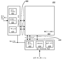
도1은 상태 변화 소자 및 안티퓨즈와 직렬인 스티어링 소자를 갖는 예시적인 2 단자 비휘발성 메모리 셀을 도시한다.
도2는 다이오드 요소들 사이에서 안티퓨즈 층을 갖는 예시적인 2 단자 비휘발성 메모리 셀을 도시한다.
도3A 및 도3B는 각각 3차원 메모리 어레이의 투시도 및 단면도이다.
도4A는 본 발명의 일실시예에 따른 비휘발성 메모리 어레이의 일부분에 대한 투시도이다.
도4B는 도4A의 비휘발성 메모리의 또 다른 투시도로서, 비휘발성 메모리 동작 동안, 비선택 필라와 선택 필라에서 정공 전류 흐름을 도시한 것이다.
도5는 필라의 높이에 대한 함수로서 비선택 어레이 라인들에서의 정공 전류를 도시한 그래프이다.
도6A 내지 도6I는 본 발명의 일실시예에 따른 비휘발성 메모리 어레이의 제조공정을 도시한 단면도들이다.
도7은 본 발명의 일실시예에 따른 비휘발성 메모리 어레이의 블록도이다. Figure 1 shows an exemplary two terminal nonvolatile memory cell having a state change element and a steering element in series with the antifuse.
2 illustrates an exemplary two terminal nonvolatile memory cell with an antifuse layer between diode elements.
3A and 3B are perspective and cross-sectional views, respectively, of a three-dimensional memory array.
4A is a perspective view of a portion of a nonvolatile memory array in accordance with an embodiment of the present invention.
FIG. 4B is another perspective view of the nonvolatile memory of FIG. 4A, illustrating hole current flow in the non-selected pillars and the selected pillars during nonvolatile memory operation.
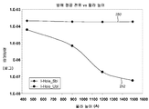
5 is a graph showing hole currents in unselected array lines as a function of pillar height.
6A through 6I are cross-sectional views illustrating a manufacturing process of a nonvolatile memory array in accordance with an embodiment of the present invention.
7 is a block diagram of a nonvolatile memory array in accordance with an embodiment of the present invention.
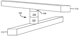
도1은 상부 전도체와 하부 전도체 사이의 교차점에 형성된 층들의 필라(100)를 포함하는 2 단자 비휘발성 메모리 셀의 예시적인 구조를 도시한다. 메모리 셀의 제 1 단자 부분은 제 1 전도체(110)에 연결되며 그리고 메모리 셀의 제 2 단자 부분은 제 2 전도체(112)에 연결된다. 상태 변화 소자(104) 및 안티-퓨즈(anti-fuse)(106)와 직렬인 스티어링 소자(102)를 포함하는 메모리 셀은 필라(100)와 함께 확장(co-extensive)하여, 비휘발성 데이터 저장소를 제공한다. Figure 1 shows an exemplary structure of a two terminal nonvolatile memory cell comprising a
스티어링 소자는, 간단한 다이오드처럼 비선형 전도 전류 특성을 나타내는 임의의 적절한 디바이스의 형태를 취할 수 있다. 상태 변화 소자는 실시예에 따라 달라질 것이며 그리고 대표적인 물리적 상태를 통해 데이터를 저장하는 수 많은 유형의 물질들을 포함할 수 있다. 상태 변화 소자(104)는 저항 변화 물질(resistance change material), 상 변화 저항성 물질(phase change resistive material) 등등을 포함할 수 있다. 2개 이상의 검출가능한 저항 변화 레벨(예컨대, 로우에서 하이로 그리고 하이에서 로우로)을 갖는 반도체 혹은 다른 물질이 수동형 저장 소자를 형성하는데 이용될 수 있다. 저항 변화 소자(104)에 세팅되고 그리고 저장 변화 소자(104)로부터 판독될 수 있는 다양한 저항 레벨들에게 논리 데이터 값들을 할당함으로써, 필라(100)로 구성되는 메모리 셀은 신뢰성 있는 데이터 기입/판독 능력을 제공할 수 있다. 또한, 안티-퓨즈(106)는 비휘발성 데이터 저장을 위해 활용될 수 있는, 저항 상태 변경 능력들을 제공할 수 있다. 안티-퓨즈는 고저항 상태로 제작되며 그리고 터지거나(popped) 혹은 융해(fused)되어 저저항 상태가 될 수 있다. 일반적으로, 안티퓨즈는 그 초기 상태에서는 비전도성이며 그리고 터진 상태 혹은 녹은 상태에서는 저저항의 고전도도를 나타낸다. 개별 디바이스 혹은 소자는 저항(resistance) 및 상이한 저항 상태(resistance state)들을 가질 수도 있으므로, 비저항(resistivity) 및 비저항 상태(resistivity state)라는 용어는, 물질 자체의 속성을 나타내는데 이용된다. 따라서, 저항 변화 소자 혹은 디바이스는 저항 상태들을 가질 수 있는 반면에, 비저항 변화 물질(resistivity change material)은 비저항 상태들을 가질 수 있다. 예를 들어, 유전체 파열(rupture) 안티퓨즈, 진성 혹은 약하게 도핑된 다결정 반도체 안티퓨즈, 그리고 비정질 반도체 안티퓨즈 등등과 같은 다양한 유형의 안티퓨즈들이 사용될 수 있지만, 이에 한정되는 것은 아니다. The steering element can take the form of any suitable device exhibiting nonlinear conduction current characteristics, such as a simple diode. State change elements will vary from one embodiment to another and can include many types of materials that store data through representative physical states. The
안티퓨즈(160)는 그 자신의 상태 변화 능력 이외에도 메모리 셀(100)에게 이점들을 제공할 수 있다. 예를 들어, 안티퓨즈는 메모리 셀에 관련된 판독-기입 회로에 대응되는 적절한 레벨로 메모리 셀의 온-저항(on-resistance)을 세팅하는데 이바지할 수도 있다. 통상적으로 이들 회로들은 안티퓨즈를 터지게하며, 그리고 이와 관련된 저항값을 갖는다. 이들 회로들이 안티퓨즈를 터트리는 전압들 및 전류 레벨들을 구동하기 때문에, 상기 안티퓨즈는 후속 동작 동안 이들 동일한 회로들에 대해서는 적절한 온-저항 상태로 메모리 셀을 세팅하는 경향이 있다. Antifuse 160 may provide benefits to
다양한 물질들이, 상태 변화 소자(104)를 구현하기에 적절한 비저항 변화 거동(resistivity change behavior)을 나타낸다. 적절한 물질들의 일례는, 도핑된 반도체(예컨대, 다결정 실리콘, 좀더 일반적으로는 폴리실리콘), 전이 금속 산화물들(transition metal oxides), 복합 금속 산화물들(transition metal oxides), 프로그램가능 금속배선 연결들(programmable metallization connections), 상 변화 비저항 소자(phase change resistivity element), 유기물질 가변 저항기(orgainc material varialble resistor), 탄소 중합체 필름, 도핑된 칼코겐화합물 글래스(doped chalcogenide glass), 저항을 변화시키는 이동 원자(mobile atom)들을 포함하는 쇼트키 장벽 다이오드 등을 포함하지만, 이에 한정되는 것은 아니다. 몇몇 경우에서, 이들 물질들의 비저항(resistivity)은 제 1 방향으로만 세트(예컨대, 하이에서 로우로)될 수도 있으며, 반면에 다른 경우들에서 상기 비저항은 제 1 레벨(예컨대, 고저항)로부터 제 2 레벨(예컨대, 저저항)로 세트될 수 있으며 그리고 다시 제 1 비저항 레벨로 리셋될 수 있다. 상태 변화 소자(104)는 일실시예에서 안티퓨즈가 될 수 있다. Various materials exhibit a resistivity change behavior suitable for implementing the
디바이스들 간의 차이들을 수용하기 위해서 뿐만 아니라 설정 및 재설정 사이클링 이후의 디바이스들 내의 변동들을 수용하기 위하여, 저항값들의 범위가 하나의 물리적인 데이터 상태에 할당될 수 있다. 세트 및 리셋 이라는 용어는, 고저항의 물리적 상태에서 저저항의 물리적 상태로 소자를 변화시키는 프로세스(세트) 그리고 저저항의 물리적 상태에서 고저항의 물리적 상태로 소자를 변화시키는 프로세스(리셋)를 각각 지칭한다. In order to accommodate differences between devices as well as to accommodate variations in devices after setup and reset cycling, a range of resistance values can be assigned to one physical data state. The terms set and reset refer to a process (set) of changing a device from a high resistance physical state to a low resistance physical state and a process of changing a device from a low resistance physical state to a high resistance physical state (reset), respectively. Refer.
다른 유형의 2 단자 비휘발성 메모리 셀들이 본 발명의 실시예들에 따라 이용될 수 있다. 예를 들어, 본 발명의 일실시예는 안티퓨즈(106)를 포함하지 않으며 상태 변화 소자(104)와 스티어링 소자(102)만을 포함한다. 다른 실시예들은 안티퓨즈 대신에 혹은 안티퓨즈에 부가하여 추가의 상태 변화 소자를 포함할 수도 있다. 다양한 유형들의 적절한 메모리 셀들이 "Vertically Stacked Field Programmable Non-volatile Memory and Method of Fabrication" 라는 명칭의 미국등록특허(등록번호 US 6,034,882)에 개시되어 있다. 또한, 미국등록특허(등록번호 US 6,420,215), 2001년 6월 29일자로 출원된 "Three-Dimensional Memory Array Incorporating Serial Chain Diode Stack" 라는 명칭의 미국특허출원(출원번호 09/897,705), 그리고 2000년 4월 28일자로 출원된 "Three-Dimensional Memory Array and Method of Fabrication" 라는 명칭의 미국특허출원(출원번호 09/560,626)에 개시된 셀들을 포함하는 다양한 다른 유형의 셀들이 또한 이용될 수 있는바, 이들 미국등록특허 및 미국출원들은 본 발명에 대한 참조로서 그 전체내용이 본 명세서에 통합된다. Other types of two terminal nonvolatile memory cells may be used in accordance with embodiments of the present invention. For example, one embodiment of the present invention does not include the
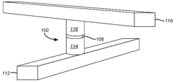
도2는 상부 전도체와 하부 전도체 사이의 교차점에서 층들의 필라로부터 형성된 2 단자 비휘발성 메모리 셀의 다른 예시적인 구조를 도시한다. 상기 일례에서 스티어링 소자는, 안티퓨즈 층(106)에 의해 분리되는 제 1 다이오드 요소(component)(114)와 제 2 다이오드 요소(116)를 갖는 다이오드이다. 이러한 배치는 때때로 초기 다이오드(incipient diode)라고 지칭된다. 이러한 다이오드는, 적절한 다이오드 접합을 형성하기에 적합한 서로다른 도전형을 갖는 물질들의 다양한 조합을 포함할 수 있다. 예를 들면, 제 1 다이오드 요소(114)는 강하게 도핑된 폴리실리콘층이 될 수 있으며 그리고 제 2 다이오드 요소는 상이한 도전형을 갖는 진성 혹은 약하게 도핑된 폴리실리콘층이 될 수 있다. 도핑되지 않은 영역들은 결함(defects)들, 오염(contaminate)들 등등 때문에 전기적으로 완벽히 중성이 아닐 수도 있는바, 상기 결함들, 오염들 등은 도핑되지 않은 영역들이 약하게 도핑된 것처럼 행동하도록 야기할 수 있다. 이러한 다이오드는 진성층(intrinsic layer)을 갖는 것으로 여전히 간주된다. 일실시예에서, 상기 제 1 다이오드 요소(114)는 강하게 도핑된 P+ 실리콘층이며 그리고 제 2 다이오드 요소는 진성 혹은 약하게 도핑된 N- 층(116)이다. 물론, 다른 실시예에서는 상기 N- 층과 P+ 층이 역전될 수 있다. 또한, 강하게 도핑된 N+ 실리콘층이 하나의 다이오드 요소를 위해 이용될 수 있으며 그리고 진성 혹은 약하게 도핑된 P- 실리콘층이 다른 하나의 다이오드 요소를 위해 이용될 수 있다. 또 다른 실시예에서는, 상기 제 2 구성요소가 강하게 도핑될 수도 있다. Figure 2 shows another exemplary structure of a two terminal nonvolatile memory cell formed from a pillar of layers at the intersection between an upper conductor and a lower conductor. In this example the steering element is a diode having a
비록, 다른 실시예에서는 상태 변화 소자가 안티퓨즈 및 다이오드에 직렬로 부가될 수도 있지만, 도2에는 상태 변화 소자(104)가 포함되어 있지 않다. 일실시예에서는, 다이오드 스티어링 소자 그 자체가 상태 변화 소자로서 이용될 수도 있다는 점을 유의해야 한다. 몇몇 메모리 셀들에서 다이오드를 형성하는데 이용되는 물질들이, 저항 변화 능력을 자체적으로 보여준다는 점이 발견되었다. 예를 들면, 일실시예에서, 다이오드의 진성 영역은 폴리실리콘으로 형성되는바, 이는 높은 비저항 상태(high resistivity state)에서 낮은 비저항 상태(low resistivity state)로 세팅되며, 이후 낮은 비저항 상태로부터 높은 비저항 상태로 리세팅되는 능력을 나타낸다. 따라서, 다이오드 그 자체 혹은 그 일부는, 메모리 셀을 위한 상태 변화 소자를 또한 형성할 수도 있다. 다른 실시예들에서는, 하나 이상의 부가층들이 메모리 셀을 위한 필라(100)에 포함되어 상태 변화 소자를 형성할 수도 있다. 예를 들면, 폴리실리콘, 전이 금속 산화물 등의 추가층들이 상태 변화 메모리 효과를 제공하도록 메모리 셀 내에 포함될 수도 있다. 이러한 추가층은 예를 들면, 다이오드 구성요소와 전도체들 중 하나 사이에 포함될 수 있다. Although in other embodiments a state change element may be added in series to the antifuse and diode, the
일반적으로, 전도체들(110, 112)은 서로 직교하며 메모리 셀들의 어레이에 액세스하기 위한 어레이 단자 라인들의 일부를 구성한다. 하나의 층에서의 어레이 단자 라인들(또는 어레이 라인들)은 워드라인들 혹은 X-라인들이라고 지칭될 수 있다. 수직으로 인접한 층에서의 어레이 라인들은 비트라인들 혹은 Y-라인들이라고 지칭될 수 있다. 메모리 셀은, 각각의 워드라인과 각각의 비트라인의 투영된 교차점에 형성될 수 있으며, 그리고 교차하는 각 워드라인 및 비트라인 사이에 도시된 바와 같이 연결되는바, 이는 필라(100)에서 메모리 셀을 형성하기 위한 것이다. 메모리 셀들의 2개 이상의 레벨들(level)(즉, 2개 이상의 메모리 평면)을 갖는 3차원 메모리 어레이는, 둘 이상의 워드라인층들 및/또는 둘 이상의 비트라인층들을 활용할 수 있다. In general, the
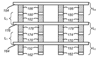
도3A 및 도3B는 예시적인 모노리식 3차원 메모리 어레이의 일부를 도시한다. 모노리식 3차원 메모리 어레이에서는, 가령, 웨이퍼와 같은 단일 기판 위에, 중간에 개재되는 기판들 없이, 복수의 메모리 레벨들이 형성된다. 도3A의 투시도에 도시된 구조에서, 워드라인층과 비트라인층 둘다는, 메모리 셀들 사이에서 공유된다. 이러한 구조는 종종 완전 미러형(fully mirrored) 구조라고 지칭된다. 실질적으로 평행하며 그리고 동일평면(coplanar)인 복수의 전도체들이 제 1 메모리 레벨(L0)에서 비트라인들(162)의 제 1 세트를 형성한다. 레벨 L0의 메모리 셀들(152)은 비트라인들과 인접 워드라인들(164) 사이에 형성된 필라를 포함한다. 도3A 및 도3B의 구조에서, 워드라인들(164)은 메모리 레벨 L0 과 메모리 레벨 L1 사이에서 공유되며, 또한 메모리 레벨 L1의 메모리 셀들(170)에 연결된다. 메모리 레벨 L1의 이들 메모리 셀들에 대해서, 전도체들의 제 3 세트가 비트라인들(174)을 형성한다. 이들 비트라인들(174)은 도3B의 단면도에 도시된 바와 같이, 메모리 레벨 L1 과 메모리 레벨 L2 사이에서 공유된다. 메모리 셀들(178)은 비트라인들(174) 및 워드라인들(176)에 연결되어 제 3 메모리 레벨 L2를 형성하며, 메모리 셀들(182)은 워드라인들(176) 및 비트라인들(180)에 연결되어 제 4 메모리 레벨 L3를 형성하며, 그리고 메모리 셀들(186)은 비트라인들(180) 및 워드라인들(184)에 연결되어 제 5 메모리 레벨 L4를 형성한다. 다이오드들의 극성 배치와 워드라인들 및 비트라인들 각각의 배치는 실시예에 따라 변할 수 있다. 또한, 5개 메모리 레벨보다 더 많거나 더 적은 메모리 레벨들이 이용될 수 있다. 3A and 3B show portions of an exemplary monolithic three dimensional memory array. In a monolithic three dimensional memory array, multiple memory levels are formed, for example, on a single substrate, such as a wafer, without intervening substrates. In the structure shown in the perspective view of Fig. 3A, both the word line layer and the bit line layer are shared between the memory cells. This structure is often referred to as a fully mirrored structure. A plurality of conductors that are substantially parallel and coplanar form a first set of
도3A의 실시예에서, 주어진 메모리 셀 레벨에 대한 다이오드 스티어링 소자는 이전 메모리 셀 레벨의 다이오드들에 비교해서 거꾸로(upside down) 형성될 수 있다. 예를 들어, 만일, 셀(152)이 P+ 타입으로 강하게 도핑된 영역인 바닥부와 진성인 혹은 약하게 도핑된 N- 타입의 최상부를 갖는다면, 셀들(170)의 제 2 레벨에서는 바닥부는 약하게 도핑된 N- 타입이 될 수 있으며, 반면에 최상부는 강하게 도핑된 P+ 타입이 될 수 있다. In the embodiment of FIG. 3A, the diode steering element for a given memory cell level can be formed upside down compared to diodes of the previous memory cell level. For example, if
대안적인 실시예에서는, 인접한 메모리 레벨들 사이에 인터-레벨(inter-level) 유전체가 형성될 수 있다. 메모리 레벨들 사이에는 그 어떤 전도체도 공유되지 않는다. 3차원 모노리식 저장 메모리를 위한 이러한 유형의 구조는 종종 비-미러형(non-mirrored) 구조라고 지칭된다. 몇몇 실시예에서, 인접 메모리 레벨들In alternative embodiments, inter-level dielectrics may be formed between adjacent memory levels. No conductor is shared between memory levels. This type of structure for three-dimensional monolithic storage memory is often referred to as a non-mirrored structure. In some embodiments, contiguous memory levels
전도체들을 공유하는 인접 메모리 레벨들과 전도체들을 공유하지 않는 인접 메모리 레벨들은 동일한 모노리식 3차원 메모리 어레이 내에 적층될 수 있다. 다른 실시예에서는, 몇몇 전도체들은 공유되지만, 반면에 다른 전도체들은 공유되지 않는다. 예를 들어, 몇몇 구성에서는 워드라인들만 혹은 비트라인들만 공유될 수 있다. 제 1 메모리 레벨 L0은 비트라인 레벨(BL0)과 워드라인 레벨(WL0) 사이에서 메모리 셀들을 포함할 수 있다. 레벨 WL0에서의 워드라인들은 메모리 레벨 L1에서 셀들을 형성하도록 공유될 수 있는바, 이는 제 2 비트라인 레벨(BL1)에 연결된다. 비트라인 층들은 공유되지 않으며, 따라서 다음 층은 다음 레벨의 전도체로부터 비트라인 BL1을 분리시키기 위한 중간층 유전체를 포함할 수 있다. 이러한 유형의 구조는 종종 하프-미러형 이라고 지칭된다. 모든 메모리 레벨들이 동일한 유형의 메모리 셀을 갖도록 형성될 필요는 없다. 필요하다면, 저항 변화 물질을 이용하는 메모리 레벨들은, 다른 유형의 메모리 셀들 이용하는 메모리 레벨들 등과 교번될 수도 있다. Adjacent memory levels that share conductors and adjacent memory levels that do not share conductors may be stacked in the same monolithic three dimensional memory array. In other embodiments, some conductors are shared while other conductors are not. For example, in some configurations only wordlines or bitlines may be shared. The first memory level L0 may include memory cells between the bitline level BL0 and the wordline level WL0. Word lines at level WL0 may be shared to form cells at memory level L1, which is coupled to second bit line level BL1. The bitline layers are not shared, so the next layer may comprise an interlayer dielectric to separate the bitline BL1 from the next level of conductor. This type of structure is often referred to as half-mirror. All memory levels need not be formed to have memory cells of the same type. If necessary, memory levels using a resistance change material may be alternated with memory levels using other types of memory cells.
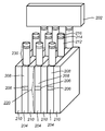
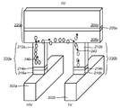
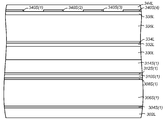
도4A는 본 발명의 일실시예에 따른 3차원 모노리식 비휘발성 메모리 어레이의 일부를 예시한다. 메모리 셀들은 제 1 전도체(202)와 제 2 전도체(204) 사이의 교차점에서 필라 구조(230)를 이용하여 형성된다. 간결함을 위해서, 오직 하나의 제 1 전도체(202)만이 도4A에 도시된다. 각각의 제 2 전도체(204)는 층들의 레일 스택(rail stack)의 일부분인바, 레일 스택은 강하게 도핑된 N+ 타입의 실리콘층(206)과 진성 혹은 약하게 도핑된 N- 타입의 실리콘층(208)을 더 포함한다. 상기 레일 스택들은, 실리콘 산화물과 같은 유전물질의 스트립(210)에 의해서 인접한 레일 스택으로부터 서로 이격된다. 강하게 도핑된 층(206)은 그 하부의 금속 전도체층(204)에게 양호한 전기적인 콘택을 제공한다. 이와 같이 강하게 도핑된 실리콘층은 오믹 천이(ohmic transition)를 중단시킬 것이며 따라서, 예컨대, 하부의 진성 혹은 약하게 도핑된 층과 금속 전도체와의 접합에서 의도하지 않은 쇼트키 다이오드의 생성을 방지할 수 있다. 다양한 도핑 기법들이 본 명세서에 개시된 도핑된 물질들을 형성하는데 이용될 수 있다. 일례로서, 증착 동안의 인-시츄(in-situ) 도핑이 일실시예에서 이용될 수 있다. 이온 주입법, 플라즈마 이머션(plasma immersion), 가스 소스 확산 혹은 고체 소스 확산 등과 같은 다른 도핑 기법들이 또한 이용될 수도 있다. 또한, 일실시예에서 어레이의 서로 다른 층들을 형성할 때에 서로 다른 도핑 기법들이 이용될 수 있다. Figure 4A illustrates a portion of a three-dimensional monolithic nonvolatile memory array in accordance with one embodiment of the present invention. Memory cells are formed using
복수의 필라 구조들(230)이 층(208) 위에 형성되는바, 각각의 필라 구조는 진성 혹은 약하게 도핑된 N- 타입 실리콘 추가층(212), 안티퓨즈층(214), 그리고 강하게 도핑된 P+ 타입 실리콘층(216)을 포함한다. P+ 타입 실리콘층(216)은 해당 필라의 메모리 셀에 대한 제 1 다이오드 요소를 형성한다. 각각의 필라의 약하게 도핑된 혹은 진성 N- 타입 실리콘층(212)은, 해당 필라의 메모리 셀에 대한 제 2 다이오드 요소의 제 1 부분을 형성한다. 각 메모리 셀에 대한 제 2 다이오드 요소는, 진성 혹은 약하게 도핑된 N- 타입 물질의 하부 스트립(208)으로부터 형성된 제 2 부분을 더 포함한다. 따라서, 이들 스트립(208)들은 제 1 방향의 길이를 따라 그 위에 놓여있는 모든 필라들에 의해 공유되어, 각각의 필라에 대해 제 2 다이오드 요소의 일부분을 형성한다. A plurality of
제 2 다이오드 요소의 일부분을 레일 스택(220)으로 이동시킴으로써, 감소된 높이를 갖는 필라가 형성된다. 메모리 셀의 전기적인 성능에 악영향을 끼침이 없이, 제 2 다이오드 요소의 소정 부분이 레일 스택으로 이동될 수 있다는 점이 발견되었다. 이러한 방식으로, 개별적인 메모리 셀들을 상부 및 하부 전도체들의 교차점에 여전히 형성할 수 있으면서도, 필라의 높이가 감소될 수 있다. 좀더 상세한 내용은, 제 2 다이오드 요소의 제 2 부분을 레일 스택에 형성하는 것의 전기적인 효과와 관련하여 후술될 것이다. By moving a portion of the second diode element to the
비록, 도4A에서 제 1 다이오드 요소는 강하게 도핑된 P+ 타입의 실리콘이고 그리고 제 2 다이오드 요소는 진성 혹은 약하게 도핑된 N- 타입 실리콘 이지만, 이와 다른 물질 조합들이 이용되어 다이오드 스티어링 소자를 형성할 수 있다. 예를 들어, 진성 혹은 약하게 도핑된 P- 타입의 물질과 강하게 도핑된 N+ 타입의 물질은 서로 짝을 이룰 수 있으며, 이는 대안적인 일례가 될 수 있다. 또한, 다른 실시예에서는, 상부 및 하부 전도체에 대한 물질들의 방향이 반전될 수도 있다. Although the first diode element in FIG. 4A is strongly doped P + type silicon and the second diode element is intrinsically or lightly doped N- type silicon, other material combinations may be used to form the diode steering element. . For example, an intrinsic or lightly doped P-type material and a strongly doped N + type material may be paired with each other, which may be an alternative example. Also, in other embodiments, the orientation of the materials relative to the upper and lower conductors may be reversed.
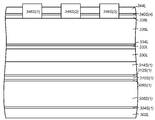
도4B는 도4A의 비휘발성 메모리의 일부분을 도시한 것으로, 공통 선택 라인들에 연결되는 비선택(unselected) 메모리 셀들을 방해함이 없이, 어레이의 메모리 셀들이 개별적으로 선택될 수 있다는 점을 예시한 도면이다. 도4B에서 어레이의 방향은 수직방향으로 뒤짚혀졌으며 그리고 표현의 간략화를 위해서 몇몇 부분들은 생략되었다. 필라(230b)에 형성된 메모리 셀은 선택하지 않으면서, 필라(230a)에 형성된 메모리 셀을 선택하기 위한 일세트의 바이어스 조건들이 도시된다. 이러한 바이어스 조건들은 예컨대, 필라(230a)에서 안티퓨즈(214a)를 터트리거나 혹은 파열시킴에 의해서 메모리 셀을 프로그램하는데 이용될 수 있다. 이러한 동작에서는, 안티퓨즈(214b)를 방해함이 없이 혹은 안티퓨즈(214b)에 영향을 미침이 없이, 안티퓨즈(214a)가 적절히 파열될 수 있도록, 필라(230a)의 메모리 셀을 충분히 격리시키는 것이 중요하다. 개시된 특정 실시예에서, 선택된 제 1 전도체(202a)에는 10V가 인가되며, 반면에 비선택 제 1 전도체(202b)에는 1V가 인가되고 그리고 선택된 전도체(204a)는 접지된다. 전도체들의 제 2 세트의 다른 비선택 전도체들(204a)(미도시)은 일실시예에서 8V의 전압을 인가받을 수 있다. 4B illustrates a portion of the nonvolatile memory of FIG. 4A, illustrating that memory cells of the array can be individually selected without disturbing unselected memory cells connected to common select lines. One drawing. In FIG. 4B the orientation of the array is flipped vertically and some parts are omitted for simplicity of representation. A set of bias conditions are shown for selecting a memory cell formed in
위와 같이 인가된 바이어스 조건하에서는, 필라(230a)를 통해 전도체(202a)로부터 전도체(204a) 방향으로 강한 전기장이 생성된다. 2개의 필라들(230a, 230b) 둘다에 전기적으로 접속된 공통 노드가 N- 층(208a)이므로, N- 층(208a)을 거쳐서 선택 전도체(202a)와 비선택 전도체(202b) 사이를 흐르는 유도 전류 흐름이 예상된다. 이러한 전류 흐름은 필라(230b)의 메모리 셀이 예기치 않게 프로그램되거나 혹은 방해받을 수 있다는 우려를 제기할 수도 있다. 하지만, 비선택 필라들의 메모리 셀들에 대한 의도하지 않은 방해를 여전히 회피할 수 있으면서도, 제 2 다이오드 요소의 소정 부분이 공통 레일 스택에 공유될 수 있다는 점이 발견되었다. Under the bias conditions applied as above, a strong electric field is generated from the
전도체(202a)와 전도체(204a) 사이의 강력한 전기장은, 화살표(240)로 도시된 전기장 방향으로의 주입 정공 전류 흐름(injection hole current flow)을 유도한다. 전도체(202b)로부터 전도체(204a)로의 방향의 전기장이 또한 비선택 필라(230b)에도 존재한다. 이 전기장은 또한, 전도체(202b)로부터 전도체(220a)로의 방향인, 화살표(242)로 표시되는 정공 전류를 유도한다. 비록, 선택 필라에서의 전기장 보다는 작지만, 비선택 필라에서의 전기장은, 주입 정공들의 대다수들이 비선택 안티퓨즈(214b)에 도달하는 것을 방해하기에는 충분히 강하다. 따라서, 필라(230b)의 메모리 셀이 방해받는 것을 방지할 수 있다. The strong electric field between
소수 확산 정공 전류가 비선택 메모리 셀들의 안티퓨즈층에 여전히 도달할 수도 있다는 점을 유의해야 한다. 하지만, 이러한 확산 전류는 거리에 따라 지수적으로 감소하므로, 소수 전류에 의해 야기될 수도 있는 임의의 방해 문제는, 필라의 높이를 적절히 선택함으로써 최소화 혹은 일소될 수 있다. 도5는 예시적인 일 구현예에서 소수 확산 정공 전류와 필라의 높이 사이의 관계를 도시한 그래프이다. 정공 전류는 필라 높이의 함수로서 y축을 따라 대수적으로(logarithmically) 표현되며, 필라 높이는 x-축을 따라 도시된다. 개시된 특정 실시예에서, 다이오드 요소의 제 2 부분 및 필라를 형성하는 N- 층의 전체 높이는 약 3000Å으로 가정된다. 필라의 높이가 감소함에 따라, 레일 스택의 N- 층의 높이는 해당하는 양만큼 증가하며 따라서, 총 높이는 약 3000Å을 유지한다. It should be noted that minority diffusion hole currents may still reach the antifuse layer of unselected memory cells. However, since this diffusion current decreases exponentially with distance, any disturbance problem that may be caused by fractional currents can be minimized or eliminated by appropriately selecting the height of the pillars. FIG. 5 is a graph illustrating the relationship between the minority diffused hole current and the height of a pillar in an exemplary embodiment. FIG. Hole currents are represented logarithmically along the y axis as a function of pillar height, and pillar height is shown along the x-axis. In the particular embodiment disclosed, the total height of the N-layer forming the pillars and the second portion of the diode element is assumed to be about 3000
인가된 바이어스 조건 하에서, 선택 전도체(202a)의 전류는 라인(250)으로 도시되며, 그리고 비선택 전도체(202b)에서의 전류는 라인(252)으로 도시된다. 필라 높이가 약 450Å 인 경우, 선택 전도체에서의 전류는 1×10⁻³ amp 보다 약간 크며, 반면에 비선택 전도체에서의 전류는 1×10⁻⁴ amp 보다 약간 작다. 비선택 필라에서의 이와 같은 전류 레벨은, 가령, 안티퓨즈(214b)를 파열시키는 것과 같이, 대응 메모리 셀들에 대한 방해를 생성할 것으로 예상될 수 있다. 필라의 높이가 증가함에 따라, 선택된 전도체에서의 전류는 대략 동일하게 유지되는 반면에, 비선택 전도체에서의 전류는 감소한다. 높이가 약 1050 Å 인 경우, 비선택 전도체에서의 전류는 약 1×10⁻⁶ amp 아래로 감소한다. 이러한 전류는 방해 문제를 야기하지 않을 정도로 충분히 낮을 수 있다. 높이가 약 1300 Å 인 경우, 비선택 전도체에서의 전류는 약 1×10⁻⁷ amp 정도로 더 감소한다. 도5에 도시된 실제 값들은 단지 예시적인 것이며, 그리고 주어진 구현예의 다른 층들의 물질들, 도핑 레벨 및 치수에 따라 변할 수 있다는 점을 유의해야 한다. 제조된 디바이스들은, 서로 다른 필라 높이에서 경험하는 방해의 정도를 특징화하기 위하여 테스트될 수도 있는바, 이는 소정 구현예에 대해서 적절한 치수를 정확하게 선택하기 위한 것이다. Under applied bias conditions, the current in
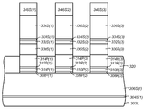
도6A 내지 도6I는 본 발명의 일실시예에 따른 모노리식 3차원 비휘발성 메모리의 제조를 예시한 도면들이다. 설명되는 제조공정은 실시예에 따라 하나 이상의 하부 메모리 레벨들을 형성한 이후에 수행될 수 있다. 도6A에 도시된 바와 같이, 절연층(302L)이 기판(미도시) 위에 형성된다. 미러형 셀 레벨 배치가 이용되는 경우와 같은 몇몇 실시예에서는 절연층(302L)이 생략될 수도 있으며, 그리고 상기 공정은 하나 이상의 선행 레벨들 위에 추가 메모리 레벨을 형성하는데 이용된다. 하부 기판은 단결정 실리콘, IV-IV 화합물, III-V 화합물, II-VII 화합물 등과 같은 임의의 반도체 기판이 될 수 있으며, 그리고 에피택셜층 혹은 기판 위에 형성된 다른 반도체층을 포함한다. 기판은 기판에 형성된 집적회로를 포함할 수도 있다. 절연층(302L)은 실리콘 이산화물, 실리콘 질화물, 고유전율(high-dielectric) 필름 등의 임의의 적절한 절연 물질을 포함할 수 있다. 6A-6I illustrate the fabrication of a monolithic three dimensional nonvolatile memory in accordance with one embodiment of the present invention. The fabrication process described may be performed after forming one or more lower memory levels in accordance with an embodiment. As shown in Fig. 6A, an insulating
선택적으로는, 절연 물질 위에 접착층(304L)이 형성되어, 전도층(306L)이 부착되는 것을 도울 수 있다. 상기 접착층은, 탄탈륨 질화물, 텅스텐 질화물, 티타늄 텅스텐, 스퍼터링된 텅스텐, 티타늄 질화물, 혹은 이들의 조합과 같은 물질들을 일례로서 포함할 수도 있지만 이에 한정되는 것은 아니다. 상기 접착층은, 화학기상증착(CVD), 물리기상증착(PVD) 혹은 원자층증착(ALD) 등과 같은 당업계에 공지된 임의의 공정에 의해서 형성될 수 있다. 일실시예에서, 접착층(304L)은 약 100Å의 두께로 증착된다. '두께' 라는 용어는, 기판(층들이 그 위에 형성됨)에 수직한 방향으로 측정된 수직 두께를 말한다. Optionally, an
CVD 혹은 PVD 등의 공지된 공정을 이용하여, 접착층(304L) 위에 전도층(306L)이 형성된다. 전도층은 당업계에 공지된 임의의 적절한 전도성 물질들, 예컨대 탄탈륨, 티타늄, 텅스텐, 구리, 코발트 혹은 이들의 합금 등과 같은 물질들을 포함할 수 있지만 이에 한정되는 것은 아니다. 비록, 두께, 물질 및 사용되는 공정이 실시예에 따라 달라질 수 있지만, 일실시예에서는 텅스텐이 CVD에 의해서 약 3000Å의 두께로 증착된다. 선택적인 접착층(308L)이 제 1 전도층(306L) 위에 약 100Å의 두께로 형성된다. 접착층(308L)은 접착층(304L)에 대해서 설명된 물질과는 다른 물질들로 구성될 수 있다. 제 1 도전형을 갖는 실리콘층(310L)이 전도층(308L) 위에 형성된다. 일실시예에서, 상기 실리콘층은 강하게 도핑된 P+ 타입의 폴리실리콘층이며 그 두께는 약 200Å이다. 다른 두께들이 이용될 수 있다. 일례로서, 일실시예에서 상기 강하게 도핑된 P+ 타입 폴리실리콘층은 5×10¹⁸ 원자/㎤ 보다 큰 농도로 도핑될 수 있다. 다른 실시예에서 상기 P+ 층은 1×10¹⁹ 원자/㎤ 보다 큰 농도로 도핑될 수 있으며, 또 다른 실시예에서는 1×10²⁰ 원자/㎤ 보다 큰 농도로 도핑될 수 있다. Using a known process such as CVD or PVD, a
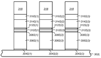
강하게 도핑된 P+ 타입 층 위에 안티퓨즈층(312L)이 형성된다. 일실시예에서 안티퓨즈 물질은 약 20-100Å의 두께로 증착되는 실리콘 이산화물이다. 다른 두께들이 이용될 수도 있다. 상기 층(310L)과는 다른 도전형을 갖는 실리콘 물질층(314L)이 안티퓨즈층 위에 형성된다. 층(314L)은 각각의 필라에서 제 2 다이오드 요소의 제 1 부분을 형성하게 될 것이다. 상기 층(310L)이 강하게 도핑된 P+ 타입 실리콘층이라면, 층(314L)은 도핑되지 않은 진성 실리콘층 혹은 반대되는 도전형의 약하게 도핑된 실리콘층(즉, 이 실시예에서는 N-)이 될 수 있다. 일실시예에서, 층(314L)은 약 1300Å의 두께로 증착된다. 상기 층(314L)이 약하게 도핑된 N- 타입의 물질인 일실시예에서, 실리콘은 5×10¹⁷ 원자/㎤ 보다 작은 농도로 도핑된다. 다른 실시예에서는, 1×10¹⁷ 원자/㎤ 혹은 1×10¹⁶ 원자/㎤ 보다 작은 농도가 이용된다. N- 층(314L) 위에 하드마스크층(316L)이 형성된다. 예컨대, 실리콘 질화물과 같은 임의의 적절한 하드마스크 물질이 이용될 수 있지만, 이에 한정되는 것은 아니다. 이후, 통상적인 포토리소그래피 기법을 이용하여, 하드마스크 위에 포토레지스트의 스트립(318)이 형성된다. 포토레지스트의 스트립들은 하드마스크 상에서 제 1 방향으로 연장되는바, 상기 제 1 방향에 실질적으로 수직한 제 2 방향으로 인접하고 있는 상기 스트립들은 그 사이에서 소정 간격을 갖는다. 또한, 일실시예에서는, 스페이서-도움(spacer-assisted) 패터닝 혹은 나노-임프린트(nano-imprint) 기법들이 이용되어, 사용되는 포토리소그래피 공정의 정의가능한 최소 피처 사이즈보다 더 작게 패턴을 형성할 수도 있다. An
포토레지스트를 패턴으로 이용하여 하드마스크층이 식각되며, 이후 도6B에 도시된 바와 같이, 그 하부층들도 식각된다. 식각공정은 절연층(302L)에 도달할 때까지 진행된다. 임의의 적절한 식각 공정 혹은 식각 공정들이 이용될 수 있다. 상기 층들은 스트립들로 식각되는바, 스트립들은 제 1 방향으로 연장되며 그리고 스트립들 사이에서 소정 간격을 갖게끔 제 2 방향으로 이격된다. 스트립의 폭은 실시예에 따라 다를 수 있지만, 일실시예에서는 약 450Å이다. 층들의 스택을 식각함에 따라, 기판 위에서 제 1 방향으로 연장되는 전도체들(306S(1) - 306S(3))의 제 1 세트가 형성된다. 상기 층들(308L, 310L, 312L, 314L, 316L) 모두가 식각되어, 스트립들(308S(1)-(3), 310S(1)-(3), 312S(1)-(3), 314S(1)-(3), 316S(1)-(3))이 형성된다. The hard mask layer is etched using the photoresist as a pattern, and then the underlying layers are etched, as shown in FIG. 6B. The etching process proceeds until it reaches the insulating
제 1 전도체들을 형성하기 위한 식각공정 이후에, 포토레지스트 및 하드마스크 스트립들(316S(1)-(3))이 제거된다. 포토레지스트를 제거하기 위하여 산소-함유 플라즈마에서의 애싱(ashing)과 같은 통상적인 공정들이 이용될 수 있으며, 이후 하드마스크층을 제거하기 위하여 화학 습식 식각과 같은 통상적인 공정들이 수행될 수 있다. 포토레지스트와 하드마스크를 제거한 이후, 도6C에 도시된 바와 같이, 스트립들 사이 및 스트립들 위에 유전물질(320)이 증착된다. 유전물질은 가령, 실리콘 이산화물, 실리콘 질화물 혹은 실리콘 산화질화물과 같은 임의의 적절한 전기적 절연물질이 될 수 있다. 예컨대, 화학기계연마(CMP)와 같은 통상적인 공정이 수행되어, 여분의 유전물질을 제거한다. 일실시예에서는, 스트립들 314S(1), 314S(2), 314S(3) 및 인접하는 스트립들을 분리시키는 유전물질의 상부 표면으로부터, 실질적으로 평탄한 표면이 형성된다. 다른 실시예에서는 도6C에 도시된 바와 같이, 스트립들 314S(1)-314S(3)의 상부 표면의 바로 아래로 유전층이 리세스된다. After the etching process to form the first conductors, the photoresist and
도6D는 도6C의 A--A 라인을 취해진 단면도로서, 제 1 방향에 따른 어레이의 단면을 도시한다. 절연층(302L) 위에 접착층 스트립 304S(1)이 놓여있으며, 그 다음으로 제 1 전도체 306S(1), 또 다른 접착층 스트립 308S(1), 강하게 도핑된 P+ 실리콘 스트립 310S(1), 안티퓨즈층 스트립 312S(1), 그리고 진성 혹은 약하게 도핑된 실리콘 스트립 314S(1)이 놓여있다. FIG. 6D is a cross sectional view taken along the line A-A in FIG. 6C, showing a cross section of the array along the first direction. An
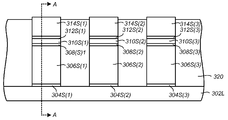
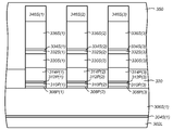
이후, 스트립 314S(1) 위에, 층(310L)과는 다른 도전형을 갖는 물질의 제 2 층(330L)이 형성된다. 층(330L)은 물질(314L)과 동일한 도전형을 가지며 그리고 복수 메모리 셀들을 위한 제 2 다이오드 요소의 제 2 부분을 형성할 것이다. 일실시예에서, 상기 층(330L)은 약하게 도핑된 N- 실리콘의 제 2 층이며, 층(314L)의 도판트 농도와 실질적으로 유사한 도판트 농도를 갖는다. 일실시예에서, 상기 층(330L)은 약 1300Å 이지만, 두께는 실시예에 따라 달라질 수 있다. 강하게 도핑된 층(332L)이, 가령, CVD와 같은 통상적인 공정을 이용하여 상기 층(330L) 위에 형성된다. 일실시예에서 상기 층(332L)은, 강하게 도핑된 N+ 타입의 실리콘층인바, 이는 그 위의 전도층과의 양호한 전기적 콘택을 제공하며 그리고 쇼트키 다이오드의 형성을 방지한다. 일실시예에서, 층(332L)은 약 200Å의 두께로 형성된다. 상기 층(332L) 위에는 접착층(334L)이 형성된다. 일실시예에서, 접착층은 약 100Å의 깊이로 증착된 TiN 층이다. 하지만, 층(304L)과 관련하여 전술한 바와 같이, 다른 물질들 및 다른 두께들이 이용될 수도 있다. 이후, 상기 접착층 위에 제 2 전도층(336L)이 형성된다. 일실시예에서, 제 2 전도층(336L)은 CVD 혹은 PVD을 이용하여 약 3000Å 두께로 증착된 텅스텐이다. 제 1 전도층(306L)에 대해서 설명된 바와 같이, 다른 물질들, 다른 공정들 및 다른 치수들이 이용될 수도 있다. A
일련의 다음 공정들이 이용되어, 상기 층들(336L, 334L, 332L, 330L)을 레일 스택들의 제 2 세트로 식각하기 위한 패턴이 형성될 수 있다. 상기 패턴은 또한 스트립들 314S, 312S, 310S, 308S을 필라들로 식각하는데에도 이용된다. 먼저, 전도층(336L) 위에 실리콘층(338L)이 약 300Å의 두께로 증착된다. 선택적인 접착층이 상기 전도층(336L)과 실리콘층(338L) 사이에 형성될 수 있다. 이후, 산화물층(340L)이 실리콘층 위에 약 200Å의 두께로 형성된다. 다른 두께들도 이용될 수 있다. 제 2 방향으로 연장된 포토레지스트의 스트립들(342)이 산화물층 위에 형성된다. 포토레지스트의 상기 스트립들은 제 1 방향으로 소정간격만큼 이격된다. A series of subsequent processes may be used to form a pattern for etching the
포토레지스트를 마스크로 이용하여, 산화물층이 도6E에 도시된 바와 같이 실리콘층 위에서 제 2 방향으로 연장되는 스트립들 340S(1), 340S(2),340S(3)으로 식각된다. 식각 이후에, 적절한 공정을 이용하여 포토레지스트가 제거된다. 다음으로, 산화물층(340L)의 인접한 스트립들(340S) 사이의 공간 및 각 스트립의 상부 표면 위에 코발트층(344L)이 증착된다. 코발트는 식각에 대해 양호한 저항력을 나타내므로, 이는 식각에 대하여 적절한 하드마스크층을 형성할 수 있다. 일실시예에서, 코발트층(344L)은 약 500Å의 깊이로 형성된다. 코발트를 증착한 이후, 고온(예컨대, 650℃)에서 웨이퍼가 어닐링되는바, 이는 산화물층의 인접 스트립들 사이의 영역들에서 코발트 실리콘(CoSi)의 성장을 야기한다. 도6F는 어닐링 공정의 결과인 CoSi의 스트립들 346S(1), 346S(2), 346S(3)을 도시한다. Using the photoresist as a mask, the oxide layer is etched into
어닐링 이후, 코발트층(344L), 산화물층(340L), 그리고 실리콘층(338L)의 남아있는 부분들은 도6G에 도시된 바와 같이 제거된다. 일실시예에서는 화학 습식 식각이 이용되어 이들 층들을 제거한다. 선택적인(selective) 혹은 비선택적인(non-selective) 식각 공정들이 또한 이용될 수 있다. CoSi의 스트립들은 이후 하부 층들을 식각하기 위한 마스크로서 이용될 수 있다. 도6H에 도시된 바와 같이, 하부층들을 관통하여 접착층(304L)에 도달할 때까지 식각공정이 진행된다. 일실시예에서는 선택적인 식각 공정이 이용되어, 제 1 식각공정으로부터 형성된 스트립들 사이의 공간들을 충전하는데 이용되었던 유전물질(320)을 식각함이 없이, 이들 층들을 식각한다. 전도층(336L)을 식각함으로써, 전도체들 336S(1), 336S(2), 336S(3)의 제 2 세트가 형성되는바, 상기 전도체들은 기판을 가로질러 제 2 방향으로 연장되며 그리고 전도체들 사이에서 소정 간격들을 갖도록 제 1 방향으로 이격된다. 전도체들의 제 2 세트는 레일 스택들의 세트의 일부분인바, 레일 스택은 접착층(334L)의 스트립들 334S(1)-334S(3), 강하게 도핑된 N+ 타입 오믹 콘택층(332L)의 스트립들 332S(1)-332S(3), 및 진성 혹은 약하게 도핑된 층(330L)의 스트립들 330S(1)-330S(3)을 더 포함한다. 스트립들 314S(1), 312S(1), 310S(1), 및 308S(1)을 식각하는 것을 필라들을 형성한다. 제 1 필라는 308P(1), 310P(1), 312P(1), 314P(1) 영역으로부터 형성되며, 제 2 필라는 308P(2), 310P(2), 312P(2), 314P(2) 영역으로부터 형성되며, 그리고 제 3 필라는 308P(3), 310P(3), 312P(3), 314P(3) 영역으로부터 형성된다. After annealing, the remaining portions of
식각 이후에, 유전물질의 또 다른 층(350)이 레일 스택들 및 필라들 위와 레일 스택들 및 필라들 사이에 형성된다. 가령, 실리콘 산화물과 같은 임의의 적절한 전기적 절연 물질이 이용될 수 있다. 인터-레벨(inter-level) 유전층을 형성하기 위하여, 추가적인 유전층이 유전층(350) 위에 형성될 수도 있는데, 이는 방금 형성된 메모리 레벨을 후속으로 형성되는 메모리 레벨로부터 격리시키기 위한 것이다. 다른 실시예에서는 인터-레벨 유전층이 형성되지 않으며, 따라서 미러형 혹은 하프-미러형 배치에서 전도체들 336S(1) 등은 다음 메모리 레벨에 의해 공유될 수 있다. 비록, 필수적인 것은 아니지만, 일실시예에서 CoSi 하드마스크층은 추가 메모리 레벨들을 형성하기 이전에 제거될 수 있다. After etching, another layer of
전술한 바와 같은 제조 공정은, 다이오드 요소의 소정부분이 레일 스택에 형성된 3차원 메모리 어레이를 형성하기 위한 적절한 기법의 하나의 일례일 뿐이다. 일실시예에서는, 필라들을 위한 진성 혹은 약하게 도핑된 다이오드 요소 물질을 형성하는데 예컨대, 다마신(damascene) 공정이 이용될 수 있다. 각각이 진성 혹은 약하게 도핑된 다이오드 요소 층을 포함하는 아래쪽(lower) 레일 스택들을 형성한 이후, 산화물이 갭 필 물질로서, 레일 스택들 사이 및 아래쪽 레일 스택 위의 필라의 원하는 높이까지 레일 스택 위에 증착될 수 있다. 상기 산화물은 예컨대, 필라들을 위한 위치들을 정의하도록 프린팅함으로써, 패터닝될 수 있다. 이후, 상기 산화물이 식각되어 산화물 내에 구멍들이 정의될 수 있는데, 필라 형성을 위한 진성 혹은 약하게 도핑된 실리콘층이 상기 구멍 내에 증착된다. 이후, 앞서 설명된 바와 비슷한 방식으로 공정이 진행될 수 있다. The fabrication process as described above is just one example of a suitable technique for forming a three-dimensional memory array in which certain portions of diode elements are formed in a rail stack. In one embodiment, for example, a damascene process may be used to form the intrinsic or lightly doped diode element material for the pillars. After forming the lower rail stacks each comprising a layer of intrinsic or lightly doped diode, oxide is deposited as a gap fill material on the rail stack up to the desired height of the pillar between the rail stacks and above the bottom rail stack. Can be. The oxide can be patterned, for example by printing to define locations for pillars. The oxide may then be etched to define holes in the oxide, in which an intrinsic or lightly doped silicon layer for pillar formation is deposited in the hole. The process may then proceed in a similar manner as described above.
도7은 도4A-4A 및 도6A-6I에 개시된 바와 같이 형성될 수 있는 메모리 어레이(402)를 포함하는 예시적인 집적회로의 블록도이다. 메모리 어레이(402)의 어레이 단자 라인들은, 로우(rows)로 구성된 워드라인들의 다양한 층(들) 그리고 컬럼(column)으로 구성된 비트라인들의 다양한 층(들)을 포함한다. 집적회로(400)는 로우 제어 회로(420)를 포함하는바, 상기 로우 제어 회로(420)의 출력들(408)은 메모리 어레이(402)의 각각의 워드라인들에 연결된다. 로우 제어 회로는 M개의 로우 어드레스 신호들의 그룹 및 하나 이상의 다양한 제어 신호들을 수신하며, 그리고 로우 디코더(422), 어레이 단자 드라이버(424), 그리고 판독 및 기입(즉, 프로그래밍) 동작 둘다를 위한 블록 선택 회로(426) 등과 같은 회로들을 포함할 수 있다. 집적회로(400)는 또한, 컬럼 제어 회로(410)를 포함하는바, 상기 컬럼 제어 회로(410)의 입력/출력들(406)은 메모리 어레이(402)의 각각의 비트라인들에 연결된다. 컬럼 제어 회로(410)는 N개의 컬럼 어드레스 신호들의 그룹 및 하나 이상의 다양한 제어 신호들을 수신하며, 그리고 컬럼 디코더(412), 어레이 단자 수신기 혹은 드라이버(414), 블록 선택 회로(416), 뿐만 아니라 판독/기입 회로들 및 I/O 멀티플렉서와 같은 회로들을 포함할 수 있다. 로우 제어 회로(420)와 컬럼 제어 회로(410)와 같은 회로들은 제어 회로라고 총체적으로 지칭될 수도 있으며 혹은 메모리 어레이(402)의 다양한 어레이 단자들로 연결되기 때문에 어레이 단자 회로들이라 지칭될 수도 있다. 7 is a block diagram of an exemplary integrated circuit including a
전술한 본 발명의 상세한 설명은 예시 및 설명을 위한 목적으로 제공되었다. 배타적이거나 혹은 개시된 바로 그 형태로 본 발명을 제한하고자 의도된 것이 아니다. 전술한 가르침에 비추어 볼때 수 많은 수정예들 및 변형예들이 가능하다. 본 발명의 기술적 사상과 그의 실제적인 응용을 최적으로 설명하기 위해, 본 발명의 실시예들이 선택되었다. 따라서, 해당 기술분야의 당업자들은 다양한 실시예들을 통해서 본 발명을 가장 잘 활용할 수 있을 것이며, 고려중인 특정한 용도에 적합한 다양한 변형예들을 가장 잘 활용할 수 있을 것이다. 본 발명의 범위는 첨부된 청구항들에 의해서 정의되어야 한다. The foregoing detailed description of the invention has been presented for purposes of illustration and description. It is not intended to be exhaustive or to limit the invention to the precise form disclosed. Many modifications and variations are possible in light of the above teaching. In order to best explain the technical idea of the present invention and its practical application, embodiments of the present invention have been selected. Accordingly, those skilled in the art will be able to best utilize the present invention through various embodiments, and best utilize various modifications suitable for the specific application under consideration. The scope of the invention should be defined by the appended claims.
100: 필라 102: 스티어링 소자
104: 상태 변화 소자 106: 안티퓨즈
110: 제 1 전도체 112: 제 2 전도체
114: 제 1 다이오드 요소 116: 제 2 다이오드 요소100: pillar 102: steering element
104: state change element 106: antifuse
110: first conductor 112: second conductor
114: first diode element 116: second diode element
Claims (15)
기판 위에서 제 1 방향으로 연장되는 제 1 전도체;
제 2 전도체와 제 1 다이오드 요소의 제 1 부분을 포함하는 제 1 세트의 스트립(strips) -상기 제 1 세트의 스트립은 상기 기판 위에서 제 2 방향으로 연장되며, 상기 제 2 방향은 상기 제 1 방향에 실질적으로 수직하며-; 그리고
상기 제 1 전도체와 상기 제 1 세트의 스트립과의 사이에 형성된 필라(pillar) -상기 필라는 상기 제 1 전도체와 상기 제 1 세트의 스트립과의 사이에서 직렬로 놓이는 상기 제 1 다이오드 요소의 제 2 부분, 상태 변화 소자 및 제 2 다이오드 요소를 포함하며-
를 포함하는 집적회로 디바이스. An integrated circuit device,
A first conductor extending over the substrate in a first direction;
A first set of strips comprising a second conductor and a first portion of a first diode element, the first set of strips extending in a second direction over the substrate, the second direction being in the first direction Substantially perpendicular to; And
A pillar formed between the first conductor and the strip of the first set, wherein the pillar is a second of the first diode element lying in series between the first conductor and the strip of the first set A part, a state change element and a second diode element-
Integrated circuit device comprising a.
상기 제 1 다이오드 요소의 제 1 부분은 진성(intrinsic) 폴리실리콘층을 포함하며; 그리고
상기 제 1 다이오드 요소의 제 2 부분은 진성 폴리실리콘층을 포함하는 것을 특징으로 하는 집적회로 디바이스. The method of claim 1,
The first portion of the first diode element comprises an intrinsic polysilicon layer; And
And the second portion of the first diode element comprises an intrinsic polysilicon layer.
상기 제 2 다이오드 요소는 제 1 도전형으로 강하게(heavily) 도핑된 실리콘 영역을 포함하는 것을 특징으로 하는 집적회로 디바이스. The method according to claim 1 or 2,
And said second diode element comprises a heavily doped silicon region of a first conductivity type.
상기 제 1 세트의 스트립은,
상기 제 2 전도체와 상기 제 1 다이오드 요소의 제 1 부분과의 사이에 형성된, 제 2 도전형으로 강하게 도핑된 폴리실리콘 영역을 포함하는 것을 특징으로 하는 집적회로 디바이스. The method of claim 3,
The first set of strips,
And a heavily doped polysilicon region of a second conductivity type formed between the second conductor and the first portion of the first diode element.
상기 제 1 다이오드 요소의 제 1 부분은 제 1 도전형으로 약하게(lightly) 도핑된 폴리실리콘층을 포함하며;
상기 제 1 다이오드 요소의 제 2 부분은 제 1 도전형으로 약하게 도핑된 폴리실리콘층을 포함하며;
상기 제 2 다이오드 요소는 제 2 도전형으로 강하게 도핑된 폴리실리콘 영역을 포함하며, 상기 제 2 도전형은 상기 제 1 도전형과 반대인 것을 특징으로 하는 집적회로 디바이스. The method of claim 1,
The first portion of the first diode element comprises a polysilicon layer lightly doped with a first conductivity type;
The second portion of the first diode element comprises a polysilicon layer lightly doped with a first conductivity type;
And wherein said second diode element comprises a polysilicon region heavily doped with a second conductivity type, said second conductivity type being opposite to said first conductivity type.
상기 상태 변화 소자는 안티퓨즈인 것을 특징으로 하는 집적회로 디바이스. The method according to claim 1, 2, 3, 4 or 5,
And said state change element is an antifuse.
상기 안티퓨즈는, 상기 제 1 다이오드 요소의 제 2 부분과 상기 제 2 다이오드 요소 사이에 형성되는 것을 특징으로 하는 집적회로 디바이스. The method of claim 6,
And the antifuse is formed between a second portion of the first diode element and the second diode element.
상기 필라는,
상기 제 1 다이오드 요소, 상기 제 2 다이오드 요소 및 상기 상태 변화 소자와 직렬로 놓이는 안티퓨즈를 더 포함하는 것을 특징으로 하는 집적회로 디바이스. The method according to claim 1, 2, 3, 4 or 5,
The pillar,
And an antifuse placed in series with said first diode element, said second diode element and said state change element.
상기 제 1 전도체, 상기 제 2 전도체, 상기 제 1 다이오드 요소의 제 1 부분, 상기 제 1 다이오드 요소의 제 2 부분 및 상기 제 2 다이오드 요소는 적어도 하나의 비휘발성 메모리 셀을 형성하는 것을 특징으로 하는 집적회로 디바이스. The method according to any one of claims 1 to 8,
The first conductor, the second conductor, the first portion of the first diode element, the second portion of the first diode element and the second diode element form at least one nonvolatile memory cell. Integrated circuit devices.
상기 집적회로는 모노리식 3차원 비휘발성 메모리 어레이를 포함하며;
상기 적어도 하나의 비휘발성 메모리 셀은 상기 모노리식 3차원 비휘발성 메모리 어레이의 제 1 메모리 레벨에 형성되며; 그리고
상기 집적회로는 적어도 하나의 추가 메모리 레벨을 포함하는 것을 특징으로 하는 집적회로 디바이스. 10. The method of claim 9,
The integrated circuit comprises a monolithic three dimensional nonvolatile memory array;
The at least one nonvolatile memory cell is formed at a first memory level of the monolithic three dimensional nonvolatile memory array; And
And the integrated circuit comprises at least one additional memory level.
실질적으로 평행하며 그리고 실질적으로 동일평면(coplanar)인 복수의 제 1 전도체들을 기판 위의 제 1 높이로 형성하는 단계 -상기 제 1 전도체들은 제 1 방향으로 연장되며-;
실질적으로 평행하며 그리고 실질적으로 동일평면인 복수의 레일 스택들(rail stacks)을 기판 위의 제 2 높이로 형성하는 단계 -상기 레일 스택들은 상기 제 1 방향과 실질적으로 수직인 제 2 방향으로 연장되며, 각각의 레일 스택은 제 2 전도체와 상기 레일 스택에 관련된 복수의 다이오드들에 대한 제 1 다이오드 요소의 제 1 부분을 포함하며-; 그리고
복수의 제 1 전도체들과 복수의 레일 스택들 사이의 교차점들에 복수의 필라들을 형성하는 단계 -상기 복수의 필라들은 상기 복수의 제 1 전도체들과 제 1 레일 스택의 교차점에 형성된 제 1 세트의 필라들을 포함하고, 상기 제 1 세트의 필라들 각각은, 상기 제 1 레일 스택에 관련된 복수의 다이오드들에 대한 제 1 다이오드 요소의 제 2 부분, 제 2 다이오드 요소 및 상태 변화 소자를 포함함-
를 포함하는 집적회로 디바이스의 제조방법. As a method of manufacturing an integrated circuit device,
Forming a plurality of first conductors that are substantially parallel and substantially coplanar to a first height above the substrate, the first conductors extending in a first direction;
Forming a plurality of rail stacks that are substantially parallel and substantially coplanar to a second height above the substrate, the rail stacks extending in a second direction substantially perpendicular to the first direction; Each rail stack includes a second conductor and a first portion of a first diode element for a plurality of diodes associated with the rail stack; And
Forming a plurality of pillars at intersections between the plurality of first conductors and the plurality of rail stacks, wherein the plurality of pillars are formed of a first set formed at the intersection of the plurality of first conductors and the first rail stack. Pillars, each of the first set of pillars including a second portion of a first diode element, a second diode element, and a state change element for a plurality of diodes associated with the first rail stack;
Method of manufacturing an integrated circuit device comprising a.
상기 제 1 세트의 필라들의 각 필라의 상기 제 2 다이오드 요소는 제 1 도전형을 갖는 강하게 도핑된 폴리실리콘층이며;
각 레일 스택의 상기 제 1 다이오드 요소의 제 1 부분은 진성 폴리실리콘층이며; 그리고
상기 제 1 세트의 필라들의 각 필라의 상기 제 1 다이오드 요소의 제 2 부분은 진성 폴리실리콘층인 것을 특징으로 하는 집적회로 디바이스의 제조방법. The method of claim 11,
The second diode element of each pillar of the first set of pillars is a heavily doped polysilicon layer having a first conductivity type;
The first portion of the first diode element of each rail stack is an intrinsic polysilicon layer; And
And a second portion of said first diode element of each pillar of said first set of pillars is an intrinsic polysilicon layer.
복수의 상기 제 1 전도체들, 상기 제 2 전도체들, 상기 제 1 다이오드 요소들, 상기 제 2 다이오드 요소들 및 상기 상태 변화 소자들은 복수의 비휘발성 메모리 셀들을 형성하며;
상기 비휘발성 반도체 메모리는 모노리식 3차원 비휘발성 메모리 어레이를 포함하며;
상기 복수의 비휘발성 메모리 셀들은 상기 모노리식 3차원 비휘발성 메모리 어레이의 제 1 메모리 레벨에 형성되며; 그리고
상기 집적회로는 적어도 하나의 추가 메모리 레벨을 포함하는 것을 특징으로 하는 집적회로 디바이스의 제조방법. The method according to claim 11 or 12, wherein
A plurality of said first conductors, said second conductors, said first diode elements, said second diode elements and said state changing elements form a plurality of nonvolatile memory cells;
The nonvolatile semiconductor memory comprises a monolithic three dimensional nonvolatile memory array;
The plurality of nonvolatile memory cells are formed at a first memory level of the monolithic three dimensional nonvolatile memory array; And
And said integrated circuit comprises at least one additional memory level.
상기 기판 위의 제 2 높이는 상기 기판 위의 제 1 높이보다 높은 것을 특징으로 하는 집적회로 디바이스의 제조방법. The method according to claim 11, 12 or 13,
And a second height above said substrate is higher than a first height above said substrate.
상기 기판 위에 제 1 전도층을 형성하는 단계;
상기 제 1 전도층 위에 강하게(heavily) 도핑된 폴리실리콘층을 형성하는 단계;
상기 강하게 도핑된 폴리실리콘층 위에 안티퓨즈층을 형성하는 단계;
상기 안티퓨즈층 위에 제 1 진성 폴리실리콘층을 형성하는 단계;
상기 제 1 진성 폴리실리콘층 위에 제 1 패턴을 적용하는 단계;
상기 제 1 패턴을 따라, 상기 제 1 전도층, 상기 강하게 도핑된 폴리실리콘층, 상기 안티퓨즈층, 상기 제 1 진성 폴리실리콘층을 식각하는 단계, 패터닝 및 식각은 제 1 방향으로 연장되는 각 층의 스트립들을 형성하며, 상기 스트립들은 복수의 제 1 전도체들을 포함하며;
상기 패터닝 및 식각 이후에, 상기 제 1 진성 폴리실리콘층 위에 제 2 진성 폴리실리콘층을 형성하는 단계;
상기 제 2 진성 폴리실리콘층 위에 제 2 전도층을 형성하는 단계;
상기 제 2 전도층 위에 제 2 패턴을 적용하는 단계;
복수의 레일 스택들을 형성하도록 상기 제 2 패턴을 따라 상기 제 2 전도층과 상기 제 2 진성 폴리실리콘층을 식각하는 단계, 상기 제 2 진성 폴리실리콘층은 각각의 레일 스택에 대해 제 1 다이오드 요소의 제 1 부분을 형성하며 그리고 상기 제 2 전도층은 각각의 레일 스택에 대해 제 2 전도체를 형성하며; 그리고
복수의 필라들을 형성하도록 상기 제 2 패턴을 따라 상기 제 1 진성 폴리실리콘층, 상기 안티퓨즈층, 및 상기 강하게 도핑된 폴리실리콘층을 식각하는 단계
를 더 포함하는 것을 특징으로 하는 집적회로 디바이스의 제조방법. The method of claim 19,
Forming a first conductive layer on the substrate;
Forming a heavily doped polysilicon layer over the first conductive layer;
Forming an antifuse layer on the heavily doped polysilicon layer;
Forming a first intrinsic polysilicon layer on the antifuse layer;
Applying a first pattern on the first intrinsic polysilicon layer;
Etching the first conductive layer, the heavily doped polysilicon layer, the antifuse layer, and the first intrinsic polysilicon layer along the first pattern, the patterning and etching each layer extending in a first direction Strips of the strip, the strips comprising a plurality of first conductors;
After the patterning and etching, forming a second intrinsic polysilicon layer on the first intrinsic polysilicon layer;
Forming a second conductive layer over the second intrinsic polysilicon layer;
Applying a second pattern on the second conductive layer;
Etching the second conductive layer and the second intrinsic polysilicon layer along the second pattern to form a plurality of rail stacks, wherein the second intrinsic polysilicon layer is formed of a first diode element for each rail stack. Forming a first portion and the second conductive layer forms a second conductor for each rail stack; And
Etching the first intrinsic polysilicon layer, the antifuse layer, and the heavily doped polysilicon layer along the second pattern to form a plurality of pillars
The method of manufacturing an integrated circuit device further comprising.
Applications Claiming Priority (2)
| Application Number | Priority Date | Filing Date | Title |
|---|---|---|---|
| US12/139,435 | 2008-06-13 | ||
| US12/139,435 US8154005B2 (en) | 2008-06-13 | 2008-06-13 | Non-volatile memory arrays comprising rail stacks with a shared diode component portion for diodes of electrically isolated pillars |
Publications (1)
| Publication Number | Publication Date |
|---|---|
| KR20110039260A true KR20110039260A (en) | 2011-04-15 |
Family
ID=40933694
Family Applications (1)
| Application Number | Title | Priority Date | Filing Date |
|---|---|---|---|
| KR1020117000959A KR20110039260A (en) | 2008-06-13 | 2009-06-02 | Non-volatile memory arrays comprising rail stacks with a shared diode component portion for diodes of electrically isolated pillars |
Country Status (7)
| Country | Link |
|---|---|
| US (2) | US8154005B2 (en) |
| EP (1) | EP2286453A1 (en) |
| JP (1) | JP2011524091A (en) |
| KR (1) | KR20110039260A (en) |
| CN (1) | CN102067315B (en) |
| TW (1) | TWI582907B (en) |
| WO (1) | WO2009152001A1 (en) |
Families Citing this family (57)
| Publication number | Priority date | Publication date | Assignee | Title |
|---|---|---|---|---|
| US8154005B2 (en) | 2008-06-13 | 2012-04-10 | Sandisk 3D Llc | Non-volatile memory arrays comprising rail stacks with a shared diode component portion for diodes of electrically isolated pillars |
| US8105867B2 (en) * | 2008-11-18 | 2012-01-31 | Sandisk 3D Llc | Self-aligned three-dimensional non-volatile memory fabrication |
| US8120068B2 (en) | 2008-12-24 | 2012-02-21 | Sandisk 3D Llc | Three-dimensional memory structures having shared pillar memory cells |
| US8139391B2 (en) | 2009-04-03 | 2012-03-20 | Sandisk 3D Llc | Multi-bit resistance-switching memory cell |
| US7978498B2 (en) * | 2009-04-03 | 2011-07-12 | Sandisk 3D, Llc | Programming non-volatile storage element using current from other element |
| US8270199B2 (en) * | 2009-04-03 | 2012-09-18 | Sandisk 3D Llc | Cross point non-volatile memory cell |
| JP2011129737A (en) * | 2009-12-18 | 2011-06-30 | Toshiba Corp | Method of manufacturing semiconductor storage device, and semiconductor storage device |
| US8198144B2 (en) * | 2010-06-11 | 2012-06-12 | Crossbar, Inc. | Pillar structure for memory device and method |
| US9224496B2 (en) | 2010-08-11 | 2015-12-29 | Shine C. Chung | Circuit and system of aggregated area anti-fuse in CMOS processes |
| US9711237B2 (en) | 2010-08-20 | 2017-07-18 | Attopsemi Technology Co., Ltd. | Method and structure for reliable electrical fuse programming |
| US10923204B2 (en) | 2010-08-20 | 2021-02-16 | Attopsemi Technology Co., Ltd | Fully testible OTP memory |
| US9025357B2 (en) | 2010-08-20 | 2015-05-05 | Shine C. Chung | Programmable resistive memory unit with data and reference cells |
| US8804398B2 (en) | 2010-08-20 | 2014-08-12 | Shine C. Chung | Reversible resistive memory using diodes formed in CMOS processes as program selectors |
| US9042153B2 (en) | 2010-08-20 | 2015-05-26 | Shine C. Chung | Programmable resistive memory unit with multiple cells to improve yield and reliability |
| US10916317B2 (en) | 2010-08-20 | 2021-02-09 | Attopsemi Technology Co., Ltd | Programmable resistance memory on thin film transistor technology |
| US9824768B2 (en) | 2015-03-22 | 2017-11-21 | Attopsemi Technology Co., Ltd | Integrated OTP memory for providing MTP memory |
| US8488359B2 (en) | 2010-08-20 | 2013-07-16 | Shine C. Chung | Circuit and system of using junction diode as program selector for one-time programmable devices |
| US9818478B2 (en) | 2012-12-07 | 2017-11-14 | Attopsemi Technology Co., Ltd | Programmable resistive device and memory using diode as selector |
| US10229746B2 (en) | 2010-08-20 | 2019-03-12 | Attopsemi Technology Co., Ltd | OTP memory with high data security |
| US9460807B2 (en) | 2010-08-20 | 2016-10-04 | Shine C. Chung | One-time programmable memory devices using FinFET technology |
| US9070437B2 (en) | 2010-08-20 | 2015-06-30 | Shine C. Chung | Circuit and system of using junction diode as program selector for one-time programmable devices with heat sink |
| US9236141B2 (en) | 2010-08-20 | 2016-01-12 | Shine C. Chung | Circuit and system of using junction diode of MOS as program selector for programmable resistive devices |
| US9496033B2 (en) | 2010-08-20 | 2016-11-15 | Attopsemi Technology Co., Ltd | Method and system of programmable resistive devices with read capability using a low supply voltage |
| US9019742B2 (en) | 2010-08-20 | 2015-04-28 | Shine C. Chung | Multiple-state one-time programmable (OTP) memory to function as multi-time programmable (MTP) memory |
| US8559208B2 (en) | 2010-08-20 | 2013-10-15 | Shine C. Chung | Programmably reversible resistive device cells using polysilicon diodes |
| US9431127B2 (en) | 2010-08-20 | 2016-08-30 | Shine C. Chung | Circuit and system of using junction diode as program selector for metal fuses for one-time programmable devices |
| US10249379B2 (en) | 2010-08-20 | 2019-04-02 | Attopsemi Technology Co., Ltd | One-time programmable devices having program selector for electrical fuses with extended area |
| US9251893B2 (en) | 2010-08-20 | 2016-02-02 | Shine C. Chung | Multiple-bit programmable resistive memory using diode as program selector |
| US8830720B2 (en) | 2010-08-20 | 2014-09-09 | Shine C. Chung | Circuit and system of using junction diode as program selector and MOS as read selector for one-time programmable devices |
| JP5422534B2 (en) * | 2010-10-14 | 2014-02-19 | 株式会社東芝 | Nonvolatile resistance change element and method of manufacturing nonvolatile resistance change element |
| US8988965B2 (en) | 2010-11-03 | 2015-03-24 | Shine C. Chung | Low-pin-count non-volatile memory interface |
| US9019791B2 (en) | 2010-11-03 | 2015-04-28 | Shine C. Chung | Low-pin-count non-volatile memory interface for 3D IC |
| US8913449B2 (en) | 2012-03-11 | 2014-12-16 | Shine C. Chung | System and method of in-system repairs or configurations for memories |
| US8923085B2 (en) | 2010-11-03 | 2014-12-30 | Shine C. Chung | Low-pin-count non-volatile memory embedded in a integrated circuit without any additional pins for access |
| TWI478168B (en) * | 2010-12-08 | 2015-03-21 | Chien Shine Chung | Anti-fuse cell and electronics system |
| US10586832B2 (en) | 2011-02-14 | 2020-03-10 | Attopsemi Technology Co., Ltd | One-time programmable devices using gate-all-around structures |
| US10192615B2 (en) | 2011-02-14 | 2019-01-29 | Attopsemi Technology Co., Ltd | One-time programmable devices having a semiconductor fin structure with a divided active region |
| US8848423B2 (en) | 2011-02-14 | 2014-09-30 | Shine C. Chung | Circuit and system of using FinFET for building programmable resistive devices |
| JP2013065772A (en) * | 2011-09-20 | 2013-04-11 | Toshiba Corp | Semiconductor device manufacturing method |
| US8912576B2 (en) | 2011-11-15 | 2014-12-16 | Shine C. Chung | Structures and techniques for using semiconductor body to construct bipolar junction transistors |
| US9136261B2 (en) | 2011-11-15 | 2015-09-15 | Shine C. Chung | Structures and techniques for using mesh-structure diodes for electro-static discharge (ESD) protection |
| US9324849B2 (en) | 2011-11-15 | 2016-04-26 | Shine C. Chung | Structures and techniques for using semiconductor body to construct SCR, DIAC, or TRIAC |
| US9007804B2 (en) | 2012-02-06 | 2015-04-14 | Shine C. Chung | Circuit and system of protective mechanisms for programmable resistive memories |
| US8861249B2 (en) | 2012-02-06 | 2014-10-14 | Shine C. Chung | Circuit and system of a low density one-time programmable memory |
| US8917533B2 (en) | 2012-02-06 | 2014-12-23 | Shine C. Chung | Circuit and system for testing a one-time programmable (OTP) memory |
| US9076526B2 (en) | 2012-09-10 | 2015-07-07 | Shine C. Chung | OTP memories functioning as an MTP memory |
| US9183897B2 (en) | 2012-09-30 | 2015-11-10 | Shine C. Chung | Circuits and methods of a self-timed high speed SRAM |
| US9324447B2 (en) | 2012-11-20 | 2016-04-26 | Shine C. Chung | Circuit and system for concurrently programming multiple bits of OTP memory devices |
| US9178143B2 (en) * | 2013-07-29 | 2015-11-03 | Industrial Technology Research Institute | Resistive memory structure |
| US9412473B2 (en) | 2014-06-16 | 2016-08-09 | Shine C. Chung | System and method of a novel redundancy scheme for OTP |
| KR102471608B1 (en) * | 2016-06-03 | 2022-11-29 | 에스케이하이닉스 주식회사 | Semiconductor memory device and operating method thereof |
| US11615859B2 (en) | 2017-04-14 | 2023-03-28 | Attopsemi Technology Co., Ltd | One-time programmable memories with ultra-low power read operation and novel sensing scheme |
| US10726914B2 (en) | 2017-04-14 | 2020-07-28 | Attopsemi Technology Co. Ltd | Programmable resistive memories with low power read operation and novel sensing scheme |
| US10535413B2 (en) | 2017-04-14 | 2020-01-14 | Attopsemi Technology Co., Ltd | Low power read operation for programmable resistive memories |
| US11062786B2 (en) | 2017-04-14 | 2021-07-13 | Attopsemi Technology Co., Ltd | One-time programmable memories with low power read operation and novel sensing scheme |
| US10770160B2 (en) | 2017-11-30 | 2020-09-08 | Attopsemi Technology Co., Ltd | Programmable resistive memory formed by bit slices from a standard cell library |
| KR20200092759A (en) | 2019-01-25 | 2020-08-04 | 삼성전자주식회사 | Variable resistance memory devices |
Family Cites Families (40)
| Publication number | Priority date | Publication date | Assignee | Title |
|---|---|---|---|---|
| AU562641B2 (en) | 1983-01-18 | 1987-06-18 | Energy Conversion Devices Inc. | Electronic matrix array |
| US5835396A (en) * | 1996-10-17 | 1998-11-10 | Zhang; Guobiao | Three-dimensional read-only memory |
| US6034882A (en) * | 1998-11-16 | 2000-03-07 | Matrix Semiconductor, Inc. | Vertically stacked field programmable nonvolatile memory and method of fabrication |
| US7157314B2 (en) * | 1998-11-16 | 2007-01-02 | Sandisk Corporation | Vertically stacked field programmable nonvolatile memory and method of fabrication |
| CN1278645A (en) * | 1999-06-22 | 2001-01-03 | 张世熹 | Memory for high-density integrated circuit |
| US6420215B1 (en) * | 2000-04-28 | 2002-07-16 | Matrix Semiconductor, Inc. | Three-dimensional memory array and method of fabrication |
| US6631085B2 (en) * | 2000-04-28 | 2003-10-07 | Matrix Semiconductor, Inc. | Three-dimensional memory array incorporating serial chain diode stack |
| US8575719B2 (en) * | 2000-04-28 | 2013-11-05 | Sandisk 3D Llc | Silicon nitride antifuse for use in diode-antifuse memory arrays |
| US6777773B2 (en) * | 2000-08-14 | 2004-08-17 | Matrix Semiconductor, Inc. | Memory cell with antifuse layer formed at diode junction |
| TW540086B (en) * | 2000-08-14 | 2003-07-01 | Matrix Semiconductor Inc | Dense arrays and charge storage devices, and methods for making same |
| US6515888B2 (en) * | 2000-08-14 | 2003-02-04 | Matrix Semiconductor, Inc. | Low cost three-dimensional memory array |
| US6627530B2 (en) * | 2000-12-22 | 2003-09-30 | Matrix Semiconductor, Inc. | Patterning three dimensional structures |
| US6356477B1 (en) * | 2001-01-29 | 2002-03-12 | Hewlett Packard Company | Cross point memory array including shared devices for blocking sneak path currents |
| US6525953B1 (en) * | 2001-08-13 | 2003-02-25 | Matrix Semiconductor, Inc. | Vertically-stacked, field-programmable, nonvolatile memory and method of fabrication |
| US6483734B1 (en) * | 2001-11-26 | 2002-11-19 | Hewlett Packard Company | Memory device having memory cells capable of four states |
| US6579760B1 (en) * | 2002-03-28 | 2003-06-17 | Macronix International Co., Ltd. | Self-aligned, programmable phase change memory |
| US7623370B2 (en) * | 2002-04-04 | 2009-11-24 | Kabushiki Kaisha Toshiba | Resistance change memory device |
| US7081377B2 (en) * | 2002-06-27 | 2006-07-25 | Sandisk 3D Llc | Three-dimensional memory |
| US6642603B1 (en) * | 2002-06-27 | 2003-11-04 | Matrix Semiconductor, Inc. | Same conductivity type highly-doped regions for antifuse memory cell |
| US6952043B2 (en) * | 2002-06-27 | 2005-10-04 | Matrix Semiconductor, Inc. | Electrically isolated pillars in active devices |
| WO2004061851A2 (en) * | 2002-12-19 | 2004-07-22 | Matrix Semiconductor, Inc | An improved method for making high-density nonvolatile memory |
| US7285464B2 (en) * | 2002-12-19 | 2007-10-23 | Sandisk 3D Llc | Nonvolatile memory cell comprising a reduced height vertical diode |
| US7005350B2 (en) * | 2002-12-31 | 2006-02-28 | Matrix Semiconductor, Inc. | Method for fabricating programmable memory array structures incorporating series-connected transistor strings |
| US6875651B2 (en) * | 2003-01-23 | 2005-04-05 | Sharp Laboratories Of America, Inc. | Dual-trench isolated crosspoint memory array and method for fabricating same |
| US6822903B2 (en) * | 2003-03-31 | 2004-11-23 | Matrix Semiconductor, Inc. | Apparatus and method for disturb-free programming of passive element memory cells |
| US6951780B1 (en) * | 2003-12-18 | 2005-10-04 | Matrix Semiconductor, Inc. | Selective oxidation of silicon in diode, TFT, and monolithic three dimensional memory arrays |
| US7410838B2 (en) * | 2004-04-29 | 2008-08-12 | Taiwan Semiconductor Manufacturing Co., Ltd. | Fabrication methods for memory cells |
| US7224013B2 (en) * | 2004-09-29 | 2007-05-29 | Sandisk 3D Llc | Junction diode comprising varying semiconductor compositions |
| US7405465B2 (en) * | 2004-09-29 | 2008-07-29 | Sandisk 3D Llc | Deposited semiconductor structure to minimize n-type dopant diffusion and method of making |
| US20060250836A1 (en) * | 2005-05-09 | 2006-11-09 | Matrix Semiconductor, Inc. | Rewriteable memory cell comprising a diode and a resistance-switching material |
| WO2008016833A2 (en) * | 2006-07-31 | 2008-02-07 | Sandisk 3D Llc | Increasing write voltage pulse operations in non-volatile memory |
| WO2008016420A2 (en) * | 2006-07-31 | 2008-02-07 | Sandisk 3D Llc | Multi-use memory cell and memory array and method for use therewith |
| KR100881292B1 (en) * | 2007-01-23 | 2009-02-04 | 삼성전자주식회사 | Resistive semiconductor memory device having three dimension stack structure and method for controlling the same |
| TW200847399A (en) * | 2007-05-21 | 2008-12-01 | Ind Tech Res Inst | Phase change memory device and method of fabricating the same |
| US7989740B2 (en) | 2008-05-16 | 2011-08-02 | Thermon Manufacturing Company | Heating cable |
| JP2009283513A (en) * | 2008-05-19 | 2009-12-03 | Toshiba Corp | Nonvolatile storage and its manufacturing method |
| US20090283739A1 (en) | 2008-05-19 | 2009-11-19 | Masahiro Kiyotoshi | Nonvolatile storage device and method for manufacturing same |
| US8154005B2 (en) | 2008-06-13 | 2012-04-10 | Sandisk 3D Llc | Non-volatile memory arrays comprising rail stacks with a shared diode component portion for diodes of electrically isolated pillars |
| US8105867B2 (en) | 2008-11-18 | 2012-01-31 | Sandisk 3D Llc | Self-aligned three-dimensional non-volatile memory fabrication |
| US8120068B2 (en) | 2008-12-24 | 2012-02-21 | Sandisk 3D Llc | Three-dimensional memory structures having shared pillar memory cells |
-
2008
- 2008-06-13 US US12/139,435 patent/US8154005B2/en not_active Expired - Fee Related
-
2009
- 2009-06-02 EP EP09763292A patent/EP2286453A1/en not_active Withdrawn
- 2009-06-02 WO PCT/US2009/046001 patent/WO2009152001A1/en active Application Filing
- 2009-06-02 CN CN2009801221973A patent/CN102067315B/en active Active
- 2009-06-02 JP JP2011513573A patent/JP2011524091A/en active Pending
- 2009-06-02 KR KR1020117000959A patent/KR20110039260A/en not_active Application Discontinuation
- 2009-06-12 TW TW098119833A patent/TWI582907B/en not_active IP Right Cessation
-
2012
- 2012-04-06 US US13/441,805 patent/US8748859B2/en active Active
Also Published As
| Publication number | Publication date |
|---|---|
| TWI582907B (en) | 2017-05-11 |
| US20120187361A1 (en) | 2012-07-26 |
| WO2009152001A1 (en) | 2009-12-17 |
| EP2286453A1 (en) | 2011-02-23 |
| US20090309089A1 (en) | 2009-12-17 |
| US8154005B2 (en) | 2012-04-10 |
| CN102067315A (en) | 2011-05-18 |
| JP2011524091A (en) | 2011-08-25 |
| CN102067315B (en) | 2013-04-24 |
| TW201007887A (en) | 2010-02-16 |
| US8748859B2 (en) | 2014-06-10 |
Similar Documents
| Publication | Publication Date | Title |
|---|---|---|
| US8748859B2 (en) | Non-volatile memory arrays comprising rail stacks with a shared diode component portion for diodes of electrically isolated pillars | |
| US7660181B2 (en) | Method of making non-volatile memory cell with embedded antifuse | |
| US7830697B2 (en) | High forward current diodes for reverse write 3D cell | |
| US7800933B2 (en) | Method for using a memory cell comprising switchable semiconductor memory element with trimmable resistance | |
| US7706177B2 (en) | Method of programming cross-point diode memory array | |
| US7800932B2 (en) | Memory cell comprising switchable semiconductor memory element with trimmable resistance | |
| US7618850B2 (en) | Method of making a diode read/write memory cell in a programmed state | |
| US7684226B2 (en) | Method of making high forward current diodes for reverse write 3D cell | |
| US7800934B2 (en) | Programming methods to increase window for reverse write 3D cell | |
| US8008700B2 (en) | Non-volatile memory cell with embedded antifuse | |
| US8072791B2 (en) | Method of making nonvolatile memory device containing carbon or nitrogen doped diode | |
| US8102694B2 (en) | Nonvolatile memory device containing carbon or nitrogen doped diode | |
| US7800939B2 (en) | Method of making 3D R/W cell with reduced reverse leakage | |
| US7759666B2 (en) | 3D R/W cell with reduced reverse leakage | |
| JP5695417B2 (en) | 3D read / write cell with reduced reverse leakage and method of making it | |
| WO2009002477A1 (en) | High forward current diodes for reverse write 3d cell and method of making thereof | |
| TWI508307B (en) | Nonvolatile memory device containing carbon or nitrogen doped diode and method of making thereof |
Legal Events
| Date | Code | Title | Description |
|---|---|---|---|
| WITN | Application deemed withdrawn, e.g. because no request for examination was filed or no examination fee was paid |