KR101487896B1 - Light-guide solar panel and method of fabrication thereof - Google Patents
Light-guide solar panel and method of fabrication thereof Download PDFInfo
- Publication number
- KR101487896B1 KR101487896B1 KR1020097024905A KR20097024905A KR101487896B1 KR 101487896 B1 KR101487896 B1 KR 101487896B1 KR 1020097024905 A KR1020097024905 A KR 1020097024905A KR 20097024905 A KR20097024905 A KR 20097024905A KR 101487896 B1 KR101487896 B1 KR 101487896B1
- Authority
- KR
- South Korea
- Prior art keywords
- light
- slab
- optical
- delete delete
- sunlight
- Prior art date
Links
- 238000004519 manufacturing process Methods 0.000 title description 10
- 230000003287 optical effect Effects 0.000 claims description 186
- 239000000463 material Substances 0.000 claims description 62
- 239000011247 coating layer Substances 0.000 claims description 12
- 229920000642 polymer Polymers 0.000 claims description 5
- 230000005540 biological transmission Effects 0.000 claims 3
- 230000000644 propagated effect Effects 0.000 abstract description 2
- 239000010410 layer Substances 0.000 description 45
- 238000000034 method Methods 0.000 description 12
- 238000013459 approach Methods 0.000 description 11
- 238000009833 condensation Methods 0.000 description 11
- 230000005494 condensation Effects 0.000 description 11
- 229910052782 aluminium Inorganic materials 0.000 description 10
- XAGFODPZIPBFFR-UHFFFAOYSA-N aluminium Chemical compound [Al] XAGFODPZIPBFFR-UHFFFAOYSA-N 0.000 description 10
- XLYOFNOQVPJJNP-UHFFFAOYSA-N water Substances O XLYOFNOQVPJJNP-UHFFFAOYSA-N 0.000 description 8
- 230000008901 benefit Effects 0.000 description 7
- 239000007789 gas Substances 0.000 description 7
- 230000009977 dual effect Effects 0.000 description 6
- 239000011521 glass Substances 0.000 description 6
- 230000007246 mechanism Effects 0.000 description 6
- 238000001542 size-exclusion chromatography Methods 0.000 description 6
- 239000000758 substrate Substances 0.000 description 6
- 239000004593 Epoxy Substances 0.000 description 5
- 238000010168 coupling process Methods 0.000 description 5
- 230000000694 effects Effects 0.000 description 5
- XKRFYHLGVUSROY-UHFFFAOYSA-N Argon Chemical compound [Ar] XKRFYHLGVUSROY-UHFFFAOYSA-N 0.000 description 4
- 239000000853 adhesive Substances 0.000 description 4
- 230000001070 adhesive effect Effects 0.000 description 4
- 230000008878 coupling Effects 0.000 description 4
- 238000005859 coupling reaction Methods 0.000 description 4
- 230000005611 electricity Effects 0.000 description 4
- 238000000465 moulding Methods 0.000 description 4
- 229920001296 polysiloxane Polymers 0.000 description 4
- 230000008569 process Effects 0.000 description 4
- 230000001902 propagating effect Effects 0.000 description 4
- 238000012546 transfer Methods 0.000 description 4
- XUIMIQQOPSSXEZ-UHFFFAOYSA-N Silicon Chemical compound [Si] XUIMIQQOPSSXEZ-UHFFFAOYSA-N 0.000 description 3
- 230000000712 assembly Effects 0.000 description 3
- 238000000429 assembly Methods 0.000 description 3
- 201000009310 astigmatism Diseases 0.000 description 3
- 230000008859 change Effects 0.000 description 3
- 230000000295 complement effect Effects 0.000 description 3
- 239000005038 ethylene vinyl acetate Substances 0.000 description 3
- 239000007788 liquid Substances 0.000 description 3
- 229910052710 silicon Inorganic materials 0.000 description 3
- 239000010703 silicon Substances 0.000 description 3
- 238000011144 upstream manufacturing Methods 0.000 description 3
- RYGMFSIKBFXOCR-UHFFFAOYSA-N Copper Chemical compound [Cu] RYGMFSIKBFXOCR-UHFFFAOYSA-N 0.000 description 2
- 229910052786 argon Inorganic materials 0.000 description 2
- 239000011248 coating agent Substances 0.000 description 2
- 238000000576 coating method Methods 0.000 description 2
- 238000000748 compression moulding Methods 0.000 description 2
- 239000012141 concentrate Substances 0.000 description 2
- 229910052802 copper Inorganic materials 0.000 description 2
- 239000010949 copper Substances 0.000 description 2
- 230000007423 decrease Effects 0.000 description 2
- 238000013461 design Methods 0.000 description 2
- 239000000428 dust Substances 0.000 description 2
- 239000008393 encapsulating agent Substances 0.000 description 2
- 239000012530 fluid Substances 0.000 description 2
- 238000009432 framing Methods 0.000 description 2
- 238000003306 harvesting Methods 0.000 description 2
- 238000011065 in-situ storage Methods 0.000 description 2
- 238000002347 injection Methods 0.000 description 2
- 239000007924 injection Substances 0.000 description 2
- 238000003780 insertion Methods 0.000 description 2
- 238000009434 installation Methods 0.000 description 2
- 239000002346 layers by function Substances 0.000 description 2
- 239000013307 optical fiber Substances 0.000 description 2
- 229920003229 poly(methyl methacrylate) Polymers 0.000 description 2
- 239000004926 polymethyl methacrylate Substances 0.000 description 2
- 238000012552 review Methods 0.000 description 2
- 239000000565 sealant Substances 0.000 description 2
- 230000001932 seasonal effect Effects 0.000 description 2
- 238000005476 soldering Methods 0.000 description 2
- 239000000243 solution Substances 0.000 description 2
- 238000001228 spectrum Methods 0.000 description 2
- 239000004812 Fluorinated ethylene propylene Substances 0.000 description 1
- VVQNEPGJFQJSBK-UHFFFAOYSA-N Methyl methacrylate Chemical compound COC(=O)C(C)=C VVQNEPGJFQJSBK-UHFFFAOYSA-N 0.000 description 1
- VYPSYNLAJGMNEJ-UHFFFAOYSA-N Silicium dioxide Chemical compound O=[Si]=O VYPSYNLAJGMNEJ-UHFFFAOYSA-N 0.000 description 1
- 238000004026 adhesive bonding Methods 0.000 description 1
- 239000002390 adhesive tape Substances 0.000 description 1
- 238000005219 brazing Methods 0.000 description 1
- DQXBYHZEEUGOBF-UHFFFAOYSA-N but-3-enoic acid;ethene Chemical compound C=C.OC(=O)CC=C DQXBYHZEEUGOBF-UHFFFAOYSA-N 0.000 description 1
- 238000005253 cladding Methods 0.000 description 1
- 230000001427 coherent effect Effects 0.000 description 1
- 238000009749 continuous casting Methods 0.000 description 1
- 230000008602 contraction Effects 0.000 description 1
- 239000002826 coolant Substances 0.000 description 1
- 238000005260 corrosion Methods 0.000 description 1
- 230000007797 corrosion Effects 0.000 description 1
- 239000002274 desiccant Substances 0.000 description 1
- 230000001627 detrimental effect Effects 0.000 description 1
- 238000010586 diagram Methods 0.000 description 1
- 238000004049 embossing Methods 0.000 description 1
- 125000003700 epoxy group Chemical group 0.000 description 1
- HQQADJVZYDDRJT-UHFFFAOYSA-N ethene;prop-1-ene Chemical group C=C.CC=C HQQADJVZYDDRJT-UHFFFAOYSA-N 0.000 description 1
- 238000001125 extrusion Methods 0.000 description 1
- 239000000835 fiber Substances 0.000 description 1
- 238000007667 floating Methods 0.000 description 1
- -1 for example Substances 0.000 description 1
- 239000012634 fragment Substances 0.000 description 1
- 239000005350 fused silica glass Substances 0.000 description 1
- 239000003292 glue Substances 0.000 description 1
- 238000013007 heat curing Methods 0.000 description 1
- 238000010438 heat treatment Methods 0.000 description 1
- 239000008236 heating water Substances 0.000 description 1
- 238000005286 illumination Methods 0.000 description 1
- 238000001746 injection moulding Methods 0.000 description 1
- 239000012212 insulator Substances 0.000 description 1
- 238000005304 joining Methods 0.000 description 1
- 238000003475 lamination Methods 0.000 description 1
- 229910052751 metal Inorganic materials 0.000 description 1
- 239000002184 metal Substances 0.000 description 1
- 229940102838 methylmethacrylate Drugs 0.000 description 1
- 239000000203 mixture Substances 0.000 description 1
- 238000012986 modification Methods 0.000 description 1
- 230000004048 modification Effects 0.000 description 1
- 239000003921 oil Substances 0.000 description 1
- 238000012856 packing Methods 0.000 description 1
- 238000000059 patterning Methods 0.000 description 1
- 229920009441 perflouroethylene propylene Polymers 0.000 description 1
- 230000000737 periodic effect Effects 0.000 description 1
- 229920001200 poly(ethylene-vinyl acetate) Polymers 0.000 description 1
- 229920000647 polyepoxide Polymers 0.000 description 1
- 230000009467 reduction Effects 0.000 description 1
- 238000007789 sealing Methods 0.000 description 1
- 229920002379 silicone rubber Polymers 0.000 description 1
- 239000004945 silicone rubber Substances 0.000 description 1
- 229910000679 solder Inorganic materials 0.000 description 1
- 238000000638 solvent extraction Methods 0.000 description 1
- 238000001029 thermal curing Methods 0.000 description 1
Images


Classifications
-
- H—ELECTRICITY
- H01—ELECTRIC ELEMENTS
- H01L—SEMICONDUCTOR DEVICES NOT COVERED BY CLASS H10
- H01L31/00—Semiconductor devices sensitive to infrared radiation, light, electromagnetic radiation of shorter wavelength or corpuscular radiation and specially adapted either for the conversion of the energy of such radiation into electrical energy or for the control of electrical energy by such radiation; Processes or apparatus specially adapted for the manufacture or treatment thereof or of parts thereof; Details thereof
- H01L31/04—Semiconductor devices sensitive to infrared radiation, light, electromagnetic radiation of shorter wavelength or corpuscular radiation and specially adapted either for the conversion of the energy of such radiation into electrical energy or for the control of electrical energy by such radiation; Processes or apparatus specially adapted for the manufacture or treatment thereof or of parts thereof; Details thereof adapted as photovoltaic [PV] conversion devices
- H01L31/054—Optical elements directly associated or integrated with the PV cell, e.g. light-reflecting means or light-concentrating means
-
- G—PHYSICS
- G02—OPTICS
- G02B—OPTICAL ELEMENTS, SYSTEMS OR APPARATUS
- G02B19/00—Condensers, e.g. light collectors or similar non-imaging optics
- G02B19/0004—Condensers, e.g. light collectors or similar non-imaging optics characterised by the optical means employed
-
- F—MECHANICAL ENGINEERING; LIGHTING; HEATING; WEAPONS; BLASTING
- F21—LIGHTING
- F21S—NON-PORTABLE LIGHTING DEVICES; SYSTEMS THEREOF; VEHICLE LIGHTING DEVICES SPECIALLY ADAPTED FOR VEHICLE EXTERIORS
- F21S11/00—Non-electric lighting devices or systems using daylight
-
- G—PHYSICS
- G02—OPTICS
- G02B—OPTICAL ELEMENTS, SYSTEMS OR APPARATUS
- G02B19/00—Condensers, e.g. light collectors or similar non-imaging optics
- G02B19/0004—Condensers, e.g. light collectors or similar non-imaging optics characterised by the optical means employed
- G02B19/0019—Condensers, e.g. light collectors or similar non-imaging optics characterised by the optical means employed having reflective surfaces only (e.g. louvre systems, systems with multiple planar reflectors)
-
- G—PHYSICS
- G02—OPTICS
- G02B—OPTICAL ELEMENTS, SYSTEMS OR APPARATUS
- G02B19/00—Condensers, e.g. light collectors or similar non-imaging optics
- G02B19/0004—Condensers, e.g. light collectors or similar non-imaging optics characterised by the optical means employed
- G02B19/0028—Condensers, e.g. light collectors or similar non-imaging optics characterised by the optical means employed refractive and reflective surfaces, e.g. non-imaging catadioptric systems
-
- H—ELECTRICITY
- H01—ELECTRIC ELEMENTS
- H01L—SEMICONDUCTOR DEVICES NOT COVERED BY CLASS H10
- H01L31/00—Semiconductor devices sensitive to infrared radiation, light, electromagnetic radiation of shorter wavelength or corpuscular radiation and specially adapted either for the conversion of the energy of such radiation into electrical energy or for the control of electrical energy by such radiation; Processes or apparatus specially adapted for the manufacture or treatment thereof or of parts thereof; Details thereof
- H01L31/02—Details
- H01L31/0232—Optical elements or arrangements associated with the device
- H01L31/02327—Optical elements or arrangements associated with the device the optical elements being integrated or being directly associated to the device, e.g. back reflectors
-
- H—ELECTRICITY
- H01—ELECTRIC ELEMENTS
- H01L—SEMICONDUCTOR DEVICES NOT COVERED BY CLASS H10
- H01L31/00—Semiconductor devices sensitive to infrared radiation, light, electromagnetic radiation of shorter wavelength or corpuscular radiation and specially adapted either for the conversion of the energy of such radiation into electrical energy or for the control of electrical energy by such radiation; Processes or apparatus specially adapted for the manufacture or treatment thereof or of parts thereof; Details thereof
- H01L31/04—Semiconductor devices sensitive to infrared radiation, light, electromagnetic radiation of shorter wavelength or corpuscular radiation and specially adapted either for the conversion of the energy of such radiation into electrical energy or for the control of electrical energy by such radiation; Processes or apparatus specially adapted for the manufacture or treatment thereof or of parts thereof; Details thereof adapted as photovoltaic [PV] conversion devices
- H01L31/054—Optical elements directly associated or integrated with the PV cell, e.g. light-reflecting means or light-concentrating means
- H01L31/0547—Optical elements directly associated or integrated with the PV cell, e.g. light-reflecting means or light-concentrating means comprising light concentrating means of the reflecting type, e.g. parabolic mirrors, concentrators using total internal reflection
-
- G—PHYSICS
- G02—OPTICS
- G02B—OPTICAL ELEMENTS, SYSTEMS OR APPARATUS
- G02B6/00—Light guides; Structural details of arrangements comprising light guides and other optical elements, e.g. couplings
- G02B6/0001—Light guides; Structural details of arrangements comprising light guides and other optical elements, e.g. couplings specially adapted for lighting devices or systems
- G02B6/0011—Light guides; Structural details of arrangements comprising light guides and other optical elements, e.g. couplings specially adapted for lighting devices or systems the light guides being planar or of plate-like form
- G02B6/0033—Means for improving the coupling-out of light from the light guide
- G02B6/0035—Means for improving the coupling-out of light from the light guide provided on the surface of the light guide or in the bulk of it
- G02B6/0038—Linear indentations or grooves, e.g. arc-shaped grooves or meandering grooves, extending over the full length or width of the light guide
-
- G—PHYSICS
- G02—OPTICS
- G02B—OPTICAL ELEMENTS, SYSTEMS OR APPARATUS
- G02B6/00—Light guides; Structural details of arrangements comprising light guides and other optical elements, e.g. couplings
- G02B6/0001—Light guides; Structural details of arrangements comprising light guides and other optical elements, e.g. couplings specially adapted for lighting devices or systems
- G02B6/0011—Light guides; Structural details of arrangements comprising light guides and other optical elements, e.g. couplings specially adapted for lighting devices or systems the light guides being planar or of plate-like form
- G02B6/0075—Arrangements of multiple light guides
- G02B6/0078—Side-by-side arrangements, e.g. for large area displays
-
- Y—GENERAL TAGGING OF NEW TECHNOLOGICAL DEVELOPMENTS; GENERAL TAGGING OF CROSS-SECTIONAL TECHNOLOGIES SPANNING OVER SEVERAL SECTIONS OF THE IPC; TECHNICAL SUBJECTS COVERED BY FORMER USPC CROSS-REFERENCE ART COLLECTIONS [XRACs] AND DIGESTS
- Y02—TECHNOLOGIES OR APPLICATIONS FOR MITIGATION OR ADAPTATION AGAINST CLIMATE CHANGE
- Y02E—REDUCTION OF GREENHOUSE GAS [GHG] EMISSIONS, RELATED TO ENERGY GENERATION, TRANSMISSION OR DISTRIBUTION
- Y02E10/00—Energy generation through renewable energy sources
- Y02E10/50—Photovoltaic [PV] energy
- Y02E10/52—PV systems with concentrators
-
- Y—GENERAL TAGGING OF NEW TECHNOLOGICAL DEVELOPMENTS; GENERAL TAGGING OF CROSS-SECTIONAL TECHNOLOGIES SPANNING OVER SEVERAL SECTIONS OF THE IPC; TECHNICAL SUBJECTS COVERED BY FORMER USPC CROSS-REFERENCE ART COLLECTIONS [XRACs] AND DIGESTS
- Y10—TECHNICAL SUBJECTS COVERED BY FORMER USPC
- Y10T—TECHNICAL SUBJECTS COVERED BY FORMER US CLASSIFICATION
- Y10T29/00—Metal working
- Y10T29/49—Method of mechanical manufacture
- Y10T29/49826—Assembling or joining
Landscapes
- Physics & Mathematics (AREA)
- General Physics & Mathematics (AREA)
- Engineering & Computer Science (AREA)
- Computer Hardware Design (AREA)
- Power Engineering (AREA)
- Microelectronics & Electronic Packaging (AREA)
- Condensed Matter Physics & Semiconductors (AREA)
- Electromagnetism (AREA)
- Optics & Photonics (AREA)
- Sustainable Development (AREA)
- General Engineering & Computer Science (AREA)
- Life Sciences & Earth Sciences (AREA)
- Photovoltaic Devices (AREA)
- Optical Elements Other Than Lenses (AREA)
- Optical Couplings Of Light Guides (AREA)
- Planar Illumination Modules (AREA)
- Non-Portable Lighting Devices Or Systems Thereof (AREA)
Abstract
본 발명은, 유전체 또는 다른 투명 패널(dielectric or other transparent panel) 내부에 빛을 포획하기 위해 광-가이드 태양 전지판(light-guide solar panel: LGSP)을 사용하고, 그리고 빛을 광기전력 전지와 같은 태양 에너지 수집기(solar energy collector: SEC)로 수집하기 위해 패널 엣지들(panel edges) 중의 하나로 전파하는, 태양 에너지 시스템의 발명이다. 이것은 태양 에너지 수집기의 높이에 필적하는 두께를 가지는 매우 얇은 모듈들을 가능하게 한다. 이것은 종래의 집광형 광기전력 태양 에너지 시스템들에 태생적인 깊이 요건들(depth requirements)을 제거한다.The present invention uses a light-guide solar panel (LGSP) to trap light within a dielectric or other transparent panel, and uses light as a photovoltaic cell Is propagated to one of the panel edges for collection with a solar energy collector (SEC). This enables very thin modules with a thickness comparable to the height of the solar energy collector. This eliminates the depth requirements inherent in conventional concentrating photovoltaic solar energy systems.
Description
관련 출원들의 상호참조사항Cross reference of related applications
본 출원은, 그들 전체가 본 명세서의 참고문헌을 이루는, 2007년 5월 1일자로 출원된 미국 예비 특허 출원 제60/915,207호; 2007년 6월 8일자로 출원된 미국 예비 특허 출원 제60/942,745호; 및 2007년 7월 25일자로 출원된 미국 예비 특허 출원 제60/951,775호에 대한 우선권을 주장한다.This application is related to U.S. Provisional Patent Application No. 60 / 915,207, filed May 1, 2007, the entirety of which is incorporated herein by reference. US Provisional Patent Application No. 60 / 942,745, filed June 8, 2007; And U.S. Provisional Patent Application No. 60 / 951,775, filed July 25, 2007, the contents of which are incorporated herein by reference.
발명의 분야Field of invention
본 발명은 일반적으로 말해서 태양 전지판들에 관한 것이다. 더욱 상세하게는, 본 발명은 광-가이드 집광기 태양 전지판들(light-guiding concentrator solar panels)에 관한 것이다.The present invention relates generally to solar panels. More particularly, the present invention relates to light-guiding concentrator solar panels.
발명의 배경BACKGROUND OF THE INVENTION
태양에 직접적으로 노출된 넓은 표면적에 걸쳐서 배열된 광기전력 전지들(photovoltaic (PV) cells)을 구비한 태양 전지판 어셈블리들이 공지되어 있다. 그러나, 광기전력 전지 재료가 비싸기 때문에, 태양 전지판들에 필요한 광기전력 전지 재료의 양을 감소시키기 위한 해결책들이 모색되어 왔다. 이러한 해결책들 중 의 하나는, 더 작은 표면적(이와 상응하게 더 작아진 광기전력 전지에 의해 점유됨) 위에 태양광을 집광시키기 위해, 렌즈들 및 반사경들(mirrors)과 같은 집광 광학 부재들(concentrating optical elements)을 사용한다. 집광 광학 부재들이 모두 0이 아닌(non-zero) 초점 거리(focal length)를 가질 경우, 그들은 그들의 비-집광형 대응물들(non-concentrating counterparts) 보다 실질적으로 더 부피가 큰(bulkier) 집광 광기전력 전지 모듈들(concentrated photovoltaic (CPV) modules)을 가져온다. 이러한 거대 부피 특성(bulkiness)은, CPV 모듈들의 취급에 있어서 뿐만 아니라 재료비에 있어서도 불리하다. 광기전력 전지의 크기를 감소시킴으로써 동일한 집광 계수(concentration factor)를 유지하면서도 부피가 덜 큰(less bulky) CPV 모듈들을 얻는 것이 가능하나, 광기전력 전지들을 더 작은 전지들로 다이싱(dicing) 하는 것은, 모듈들의 복잡성과 원가를 증가시킨다.Solar panel assemblies with photovoltaic (PV) cells arranged over a large surface area directly exposed to the sun are known. However, since the photovoltaic cell material is expensive, a solution has been sought to reduce the amount of the photovoltaic cell material required for the solar cell panels. One of these solutions is to concentrate the light concentrating elements, such as lenses and mirrors, to condense sunlight onto a smaller surface area (correspondingly occupied by a smaller photovoltaic cell) optical elements. When the condensing optical members all have a non-zero focal length, they are substantially bulkier than their non-concentrating counterparts, And fetches concentrated photovoltaic (CPV) modules. This large bulkiness is disadvantageous not only in handling CPV modules but also in material cost. By reducing the size of a photovoltaic cell it is possible to obtain less bulky CPV modules while maintaining the same concentration factor, but dicing photovoltaic cells into smaller cells , Increasing the complexity and cost of the modules.
또한, 현재의 CPV 모듈들은, 일반적으로 모든 부재들을 적소에 수용하기 위해 집광 광학 부재들을 복잡한 구조의 인클로저(enclosure)에 고정할 필요가 있다. 이것은 항상 CPV 모듈들의 중량과 원가를 가중시키며, 조립된 CPV 모듈들의 파손 위험을 경감시키기 위해 운송 요건들을 더 엄격하게 만들거나, CPV 모듈들이 그들의 목적지까지 조립되지 않은 상태로 운송될 것을 필요로 하게 되고 그 때문에 수령 목적지에서의 조립 시간과 수고를 필요로 한다.In addition, current CPV modules generally require fixing the condensing optical elements to an enclosure of a complicated structure in order to accommodate all members in place. This always adds to the weight and cost of the CPV modules and makes the shipping requirements more stringent to alleviate the risk of breakage of the assembled CPV modules or requires the CPV modules to be transported unassembled to their destination Therefore, it takes time and time to assemble at the receiving destination.
그러므로, 현존하는 CPV 모듈들 보다 부피가 덜 큰 CPV 모듈을 제공하는 것이 바람직하다. 공지되어 있는 CPV 모듈들 보다 비교적 더 적은 광기전력 전지 재료를 필요로 하는 CPV 모듈을 만드는 것이 또한 바람직하다. 나아가, 공지된 CPV 모듈들보다 부피가 덜 크고(less voluminous) 덜 복잡한 구조의 집광 광학 부재용 인클로저를 필요로 하는 CPV 모듈을 제공하는 것이 바람직하다. Therefore, it is desirable to provide CPV modules that are less bulky than existing CPV modules. It is also desirable to make CPV modules that require relatively less photovoltaic cell material than known CPV modules. Furthermore, it is desirable to provide a CPV module that requires an enclosure for a condensing optical member with a less voluminous and less complex structure than known CPV modules.
발명의 요약SUMMARY OF THE INVENTION
본 발명의 목적은, 종래의 태양 전지판들의 적어도 하나의 단점을 제거하거나 완화시키는 것이다.It is an object of the present invention to eliminate or alleviate at least one disadvantage of conventional solar panels.
첫 번째 측면에 있어서, 본 발명은, 빛을 수신하기 위한 하나의 입력면(input surface), 광학 부재들(optical elements) 및 적어도 하나의 광 출력공(optical output aperture)을 가지는 광-투입 스테이지(light-insertion stage)를 포함하여 구성되는 광-가이드 태양 전지판을 제공하며, 이 광학 부재들은 위의 입력면으로부터의 입력광을 위의 적어도 하나의 광 출력공으로 보내기 위해 위의 입력면과 위의 적어도 하나의 광 출력공 사이에 형성된다. 이러한 전지판은, 하나의 출력면(output surface)을 가지는 광 도파 스테이지(optical waveguide stage)를 더 포함하여 구성되며, 광 도파 스테이지는, 출력면을 향해 빛을 가이드하기 위한 것으로서, 적어도 하나의 광 출력공에 광학적으로 결합되어(optically coupled) 그로부터 빛을 수신한다.In a first aspect, the present invention provides a light-input stage having an input surface for receiving light, optical elements and at least one optical output aperture, guiding solar panel comprising a light-insertion stage and a light-insertion stage, wherein the optical members comprise at least an input surface above the input surface for transmitting input light from the input surface to the at least one light output hole, And is formed between one optical output hole. The solar panel may further comprise an optical waveguide stage having an output surface, the optical waveguide stage for guiding light toward the output surface, the at least one optical output And optically coupled to the ball to receive light therefrom.
본 발명의 태양 전지판은, 실질적으로 평행인 선들을 따라 서로 떨어져 있는 광학 부재들을 가질 수 있으며, 출력면은 입력면에 대해 실질적으로 직교하지 않을 수 있다.The solar panel of the present invention may have optical members that are spaced apart along substantially parallel lines, and the output surface may not be substantially orthogonal to the input surface.
본 발명의 태양 전지판은, 실질적으로 동심원인 원호들(circle arcs)을 따라 서로 떨어져 있는 광학 부재들을 가질 수 있으며, 출력면은, 광학 부재들과 실질적으로 동심원인(concentric) 원호의 형상을 가질 수 있다.The solar panel of the present invention may have optical members that are spaced apart from one another along substantially concentric circular arcs and the output surface may have a shape of a circular arc that is substantially concentric with the optical members have.
본 발명의 태양 전지판은, 포물선형 반사판들(parabolic reflectors), 3차원 반사판들(cubic reflectors), 쌍곡선형 반사판들(hyperbolic reflectors), 타원형 반사판들(elliptical reflectors), 평탄 반사판들(flat reflectors), 카세그레인 광학계들(Cassegrain optics), 윈스턴 콘 광학계들(Winston cone optics), 원형 반사판들, 렌즈들, 홀로그램(hologram) 및 프리즘 리지들(prismatic ridges) 중의 적어도 하나를 포함하는 광학 부재들을 가질 수 있다.The solar panel of the present invention can be used in various applications such as parabolic reflectors, cubic reflectors, hyperbolic reflectors, elliptical reflectors, flat reflectors, Optical elements including at least one of Cassegrain optics, Winston cone optics, circular reflectors, lenses, holograms and prismatic ridges.
본 발명의 태양 전지판은 쐐기-형상(wedge-shaped) 광 도파 스테이지를 가질 수 있다. 본 발명의 태양 전지판은 적어도 부분적으로 원뿔-형상인(cone-shaped) 광 도파 스테이지를 가질 수 있다.The solar panel of the present invention may have a wedge-shaped optical waveguide stage. The solar panel of the present invention may have a cone-shaped optical waveguide stage that is at least partially conical.
본 발명의 태양 전지판은, 적어도 하나의 광 출력공으로부터 수신된 빛이 그로부터 제1 내부 전반사(total internal reflection)를 일으키는, 제1 면(a first surface)을 포함하는 광 도파 스테이지를 가질 수 있다. 특허청구된 태양 전지판은, 입력면과 제1 면 중의 적어도 하나가 거기에 형성된 하나의 피복층(cladding layer)를 가질 수 있다.The solar panel of the present invention may have a light waveguiding stage that includes a first surface, from which light received from at least one light output hole causes a first total internal reflection. The claimed solar panel may have a cladding layer in which at least one of the input surface and the first surface is formed.
특허청구된 태양 전지판은, 제1 면과 마주보게 형성된 복수의 반사판 부재들(reflector elements)을 구비한 광 도파 섹션(optical waveguide section)을 가질 수 있으며, 이러한 복수의 반사판 부재들은 제1 면으로부터 내부 전반사된 빛을 수신하고 그리고 상기 내부 전반사된 빛을 제1 면을 향해 반사하기 위한 것이다. 복수의 반사판 부재들은, 평면 반사판들(planar reflectors)을 포함할 수 있다. 이 평면 반사판들은 제1 면과 실질적으로 평행할 수 있다. 위의 적어도 하나의 반사 부재(reflecting element)는 하나의 내부 전반사 면(total internal reflection surface)을 가질 수 있다. 적어도 하나의 광 출력공은 인접한 반사판 부재들 사이에 위치될 수 있다.The claimed solar panel may have an optical waveguide section with a plurality of reflector elements formed opposite to the first surface, the plurality of reflector members being arranged to extend from the first surface to the inner surface, Receiving the totalized light and reflecting the total internal reflected light toward the first surface. The plurality of reflection plate members may include planar reflectors. These planar reflectors may be substantially parallel to the first surface. At least one of the above reflecting elements may have one total internal reflection surface. At least one light output aperture may be positioned between adjacent reflector members.
특허청구된 태양 전지판은, 적어도 하나의 광 출력공을 통해 광 도파 스테이지로부터 광-투입 스테이지로 실질적으로 빛이 전혀 연결되지(coupled) 않게 구성될 수 있다.The claimed solar panel can be configured so that substantially no light is coupled from the optical waveguide stage to the light-entering stage through at least one light output hole.
본 발명의 태양 전지판은, 광 도파 스테이지가 일련의(a series of) 내부 전반사들을 통해 빛을 출력면을 향해 가이드하도록 구성될 수 있다. 본 발명의 태양 전지판은, 입력면이 하나의 광 입력 구역(light input area)을 가지며, 출력면이 하나의 광 수집 구역(light collecting area)을 가지도록 구성될 수 있으며, 이러한 광 수집 구역은 광 입력 구역 보다 더 작다.The solar panel of the present invention can be configured so that the optical waveguide stage guides the light toward the output face through a series of internal total internal reflection. The solar panel of the present invention can be configured such that the input surface has one light input area and the output surface has one light collecting area, It is smaller than the input area.
본 발명의 태양 전지판은, 출력면에 광학적으로 결합된 하나의 태양 에너지 수집기(solar energy collector)를 포함하여 구성될 수 있다. 태양 에너지 수집기는, 광기전력 태양 전지(photovoltaic solar cell)와 집열기(heat collector) 중의 적어도 하나를 포함할 수 있다. 본 발명의 태양 전지판은, 출력면을 태양 에너지 수집기에 광학적으로 결합시키기 위한 하나의 광학 프리즘(optical prism)을 더 포함하여 구성될 수 있다.The solar panel of the present invention may comprise a solar energy collector optically coupled to the output surface. The solar energy collector may include at least one of a photovoltaic solar cell and a heat collector. The solar panel of the present invention may further comprise an optical prism for optically coupling the output surface to the solar energy collector.
본 발명의 태양 전지판은, 광 도파 스테이지가 출력면에 인접한 적어도 하나의 포물선-형상 인터페이스(parabolically-shaped interface)를 가지도록 구성될 수 있으며, 이러한 적어도 하나의 포물선-형상 인터페이스는 출력면에 빛을 집광시키기(concentrating) 위한 것이다. 본 발명의 태양 전지판은, 출력면에 인접한 하나의 테이퍼진(tapered) 광학 부재를 포함하여 구성될 수 있고, 이러한 테이퍼진 광학 부재는 태양 에너지 수집기를 광 도파 스테이지로부터 거리를 두기 위한 것이며 그리고 빛을 태양 에너지 수집기에 집광시키기 위한 것이다. 테이퍼진 광학 부재는, 광 도파 스테이지와 상이한 굴절률(refractive index)을 가질 수 있다.The solar panel of the present invention may be configured such that the photovoltaic stage has at least one parabolically-shaped interface adjacent to the output surface, wherein the at least one parabolic-shaped interface provides light to the output surface To concentrating it. The solar panel of the present invention may comprise one tapered optical member adjacent to the output surface, which tapered optical member is intended to distance the solar energy collector from the optical waveguide stage, To concentrate on a solar energy collector. The tapered optical member may have a refractive index different from that of the optical waveguide stage.
본 발명의 태양 전지판은, 광 도파 스테이지가 복수의 도파관들을 포함하도록 할 수 있으며, 각 도파관은, 적어도 하나의 광 출력공들 중의 하나에 광학적으로 결합되며, 각 도파관은, 하나의 상응하는 광 출력공으로부터 빛을 수신하고 그리고 적어도 광학 부재들에 의해 결정된 방향으로 도파관을 따라 빛을 전파하기 위한 것이다. 각 도파관은, 하나의 도파관 출력면을 가질 수 있으며, 도파 스테이지 출력면은 각 도파관의 도파관 출력면을 포함하여 구성된다. 광학 부재들은, 각 도파관을 따라 단지 한 방향으로 또는 각 도파관을 따라 마주보는 두 방향들로 전파되게 빛을 보낼 수 있다. 광학 부재들은 하나의 볼륨 위상 홀로그램(volume phase hologram)을 포함할 수 있다. 광학 부재들은 복수의 프리즘 리지들을 포함할 수 있다.The solar panel of the present invention may be such that the optical waveguide stage comprises a plurality of waveguides, each waveguide being optically coupled to one of the at least one optical output wells, each waveguide having one corresponding optical output Receive light from the ball and propagate the light along the waveguide in at least directions determined by the optical elements. Each waveguide may have one waveguide output surface, and the output stage of the waveguide stage includes a waveguide output surface of each waveguide. The optical elements can transmit light propagating in only one direction along each waveguide or in two directions opposite each other along each waveguide. The optical elements may include a volume phase hologram. The optical elements may comprise a plurality of prism ridges.
본 발명의 태양 전지판은, 광-투입 스테이지가 복수의 테이퍼진 광 채널들(tapered light channels)을 포함할 수 있고, 그리고 광 도파 스테이지가 복수의 도파관들을 포함할 수 있으며, 테이퍼진 광 채널들 중의 적어도 하나가 적어도 하나의 광 출력공들 중의 하나를 통해 적어도 하나의 도파관에 광학적으로 결합되고, 각 도파관이 적어도 광학 부재들에 의해 결정된 전파 방향으로 도파관을 따라 빛을 가이드하도록 구성될 수 있다. 적어도 하나의 도파관이 상이한 직경들의 도파관들을 포함할 수 있다. 광학 부재들은, 빛에 전파 방향을 부여하기 위해 볼륨 위상 홀로그램과 프리즘 리지들 중의 적어도 하나를 포함할 수 있다. 광학 부재들은, 포물선형 반사판들, 3차원 반사판들, 쌍곡선형 반사판들, 타원형 반사판들, 평탄 반사판들 및 원형 반사판들 중의 적어도 하나를 더 포함할 수 있다.The solar panel of the present invention is characterized in that the light-input stage may comprise a plurality of tapered light channels and the optical waveguide stage may comprise a plurality of waveguides, At least one of which is optically coupled to at least one waveguide through one of the at least one optical output wells and each waveguide can be configured to guide light along the waveguide in a propagation direction determined by at least optical members. At least one waveguide may comprise waveguides of different diameters. The optical members may include at least one of a volume phase hologram and prism ridges to impart a propagation direction to the light. The optical members may further include at least one of parabolic reflectors, three-dimensional reflectors, hyperbolic reflectors, elliptical reflectors, flat reflectors, and circular reflectors.
광-투입 스테이지는, 광 투과성 물질(optically transmissive material)로 된 제1 슬래브(slab)에 형성될 수 있고, 광 도파 스테이지는, 광 전송 물질로 된 제2 슬래브에 형성될 수 있다. 제1 슬래브는, 입력면과 광학 부재들을 포함할 수 있으며, 입력면과 마주 보는 하나의 출력 프로파일 면(output profiled surface)을 가질 수 있다. 제2 슬래브는, 출력 프로파일 면에 인접한 하나의 입력 프로파일 면(input profiled surface)을 포함할 수 있고, 제1 슬래브의 출력 프로파일 면과 제2 슬래브의 입력 프로파일 면은, 서로에 대해 상보적이며 적어도 하나의 광 출력공을 구획한다(define).The light-input stage may be formed in a first slab of an optically transmissive material, and the light-wave stage may be formed in a second slab of a light-transmitting material. The first slab may include an input surface and optical members and may have an output profiled surface facing the input surface. The second slab may include one input profiled surface adjacent to the output profile surface and the output profile surface of the first slab and the input profile surface of the second slab are complementary to each other and at least One optical output hole is defined.
본 발명의 태양 전지판은, 광-투입 스테이지가 광 전송 물질로 된 제1 및 제2 레이어들에 형성되고, 광 도파 스테이지가 광 전송 물질로 된 제3 레이어에 형성되도록 구성될 수 있다. 제1 레이어는, 입력면을 포함할 수 있으며, 입력면과 마주 보는 제1 프로파일 면(a first profiled surface)을 더 포함할 수 있다. 제2 레이어는, 제1 프로파일 면과 인접하고 그와 상보적인 제2 프로파일 면을 포함할 수 있으며, 제2 레이어는 제2 프로파일 면과 마주 보는 제3 프로파일 면을 더 포함할 수 있다. 제3 레이어는, 제3 프로파일 면과 인접하고 그와 상보적인 제4 프로파일 면을 포함할 수 있으며, 제3 프로파일 면과 제4 프로파일 면은 적어도 하나의 광 출력공을 구획한다.The solar panel of the present invention can be configured such that the light-input stage is formed in first and second layers made of a light-transmitting material, and the light-wave stage is formed in a third layer made of a light-transmitting material. The first layer may include an input surface and may further include a first profiled surface facing the input surface. The second layer may include a second profile surface adjacent and complementary to the first profile surface, and the second layer may further include a third profile surface facing the second profile surface. The third layer may include a fourth profile surface adjacent and complementary to the third profile surface, wherein the third profile surface and the fourth profile surface define at least one light output aperture.
본 발명의 태양 전지판은, 광-투입 스테이지와 광 도파 스테이지가 동일한 광 전송 물질로 만들어지도록 구성될 수 있다.The solar panel of the present invention can be configured so that the light-input stage and the light-wave stage are made of the same light-transmitting material.
본 발명의 태양 전지판은, 광 투입 스테이지가 제1 세트의(a first set of) 실질적으로 동심원인 원호들을 따라 서로 떨어져 있는 제1 세트의 광학 부재들을 가지는 제1 섹션(section), 그리고 제2 세트의(a second set of) 실질적으로 동심원인 원호들을 따라 서로 떨어져 있는 제2 세트의 광학 부재들을 가지는 제2 섹션을 가지도록 구성될 수 있다. 제1 세트의 광학 부재들은, 빛의 제1 부분을 제1 방향으로 보낼 수 있으며, 제2 세트의 광학 부재들은 빛의 제2 부분을 제1 방향과 전혀 다른 제2 방향으로 보낼 수 있다. 제2 방향은 제1 방향과 정반대일 수 있다. 광-투입 스테이지의 제1 섹션은 적어도 하나의 제1 섹션 광 출력공(first section optical output aperture)을 가질 수 있고, 광-투입 스테이지의 제2 섹션은 적어도 하나의 제2 섹션 광 출력공을 가질 수 있으며, 광 도파 스테이지는 적어도 하나의 제1 섹션 광 출력공에 광학적으로 결합된 제1 섹션과 적어도 하나의 제2 섹션 광 출력공에 광학적으로 결합된 제2 섹션을 가질 수 있다.The solar panel of the present invention is characterized in that the light input stage comprises a first section having a first set of optical elements spaced apart from one another along a first set of substantially concentric arcs, And a second section having a second set of optical elements spaced apart from one another along a second set of substantially concentric arcs. The first set of optical elements can direct a first portion of light in a first direction and the second set of optical elements can direct a second portion of light in a second direction that is completely different from the first direction. The second direction may be opposite to the first direction. The first section of the light-input stage may have at least one first section optical output aperture and the second section of the light-entering stage may have at least one second section light output aperture And the optical waveguide stage may have a first section optically coupled to the at least one first section optical output cavity and a second section optically coupled to the at least one second section optical output cavity.
본 발명의 다른 측면에 있어서, 빛을 수신하기 위한 하나의 입력면, 적어도 하나의 광 출력공, 및 상기 입력면과 상기 적어도 하나의 광 출력공 사이에 형성되어 상기 입력면으로부터의 입력광을 상기 적어도 하나의 광 출력공으로 보내는 광학 부재들을 가지는 하나의 광-투입 스테이지; 하나의 출력면을 가지며, 상기 출력면을 향해 빛을 가이드하기 위한 것으로서, 적어도 하나의 광 출력공에 광학적으로 결합되어 그로부터 빛을 수신하는, 하나의 광 도파 스테이지; 그리고 상기 출력면에 광학적으로 결합된 하나의 광기전력 전지;를 포함하여 구성되는, 광-가이드 태양 전지판이 제공된다.According to another aspect of the present invention, there is provided a light source device comprising: an input surface for receiving light; at least one light output hole; and a light receiving element formed between the input surface and the at least one light output hole, One light-entering stage having optical members for sending to at least one light output hole; One optical waveguide stage having one output face and guiding light toward the output face, the optical waveguide stage being optically coupled to at least one optical output cavity to receive light therefrom; And one photovoltaic cell optically coupled to the output surface. The light guide solar panel includes a plurality of photovoltaic cells.
본 발명의 또 다른 측면에 있어서, 광-가이드 태양 전지판의 제작 방법이 제공된다. 이 방법은, 빛을 수신하기 위한 하나의 입력면, 적어도 하나의 광 출력공, 및 상기 입력면과 상기 적어도 하나의 광 출력공 사이에 위치되어 상기 입력면으로부터의 입력광을 상기 적어도 하나의 광 출력공으로 보내는 광학 부재들을 가지는 하나의 광-투입 스테이지를 만드는(forming) 단계; 하나의 출력면을 가지는 하나의 광 도파 스테이지를 만드는 단계; 그리고 상기 빛을 상기 출력면을 향해 가이드하기 위한 상기 광 도파 스테이지를, 그로부터 빛을 받아들이기 위해 상기 적어도 하나의 광 출력공에 광학적으로 결합시키는 단계;를 포함하여 구성된다.In another aspect of the present invention, a method of manufacturing a light-guide solar panel is provided. The method includes the steps of: one input surface for receiving light; at least one light output aperture; and a light source positioned between the input surface and the at least one light output aperture, Forming a single light-injecting stage having optical elements for directing to an output cavity; Forming one optical waveguide stage having one output surface; And optically coupling the optical waveguide stage for guiding the light toward the output face to the at least one optical output aperture to receive light therefrom.
첨부 도면들과 함께 본 발명의 특정 실시예들에 대한 다음의 설명을 검토함에 따라 본 발명의 다른 측면들과 특성들이 이 분야의 통상의 지식을 가진 자들에게 명백하게 될 것이다.Other aspects and features of the present invention will become apparent to those skilled in the art upon review of the following description of specific embodiments of the invention in conjunction with the accompanying drawings.
지금부터 본 발명의 실시예들을 첨부된 도면들을 참조하여, 단지 예시로서만, 설명하기로 하는 바, 도면들 중에서:BRIEF DESCRIPTION OF THE DRAWINGS Embodiments of the present invention will now be described, by way of example only, with reference to the accompanying drawings, in which:
도 1은, 본 발명의 광-가이드 태양 전지판의 제1 실시예를 나타내고; 1 shows a first embodiment of a light-guide solar panel of the present invention;
도 2는, 도 1의 실시예에서 복수의 광선들이 하나의 단일 반사판(single reflector)에 의해 초점 맞추어지는(focused) 것을 보여주며;Figure 2 shows that in the embodiment of Figure 1 a plurality of light beams are focused by a single reflector;
도 3은, 도 1의 실시예의 세부사항을 나타내고;Figure 3 shows the details of the embodiment of Figure 1;
도 4는, 도 1의 실시예의 확대도를 나타내며;Figure 4 shows an enlarged view of the embodiment of Figure 1;
도 5는, 광선들이 하나의 광 도파 스테이지에 포획된 채로 있는 광-가이드 태양 전지판을 나타내고;Figure 5 shows a light-guide solar panel in which the rays of light remain trapped in one light-guide stage;
도 6은, 광선들이 광 도파 스테이지들로부터 빠져나오는(escape) 광-가이드 태양 전지판을 나타내며;Figure 6 shows a light-guide solar panel in which rays of light escape from the photodetection stages;
도 7은, 본 발명의 광-가이드 태양 전지판의 선형 형상(linear geometry) 실시예의 사시도이고;7 is a perspective view of a linear geometry embodiment of the light-guide solar panel of the present invention;
도 8A는, 두 개의 광선들이 거기에 전파되는, 도 7의 실시예의 광-가이드 태양 전지판의 측면도이며;FIG. 8A is a side view of the light-guide solar panel of the embodiment of FIG. 7, with two rays propagating therein; FIG.
도 8B는, 두 개의 광선들이 거기에 전파되는, 도 7의 실시예의 광-가이드 태양 전지판의 정면도이고;8B is a front view of the light-guide solar panel of the embodiment of Fig. 7, in which two rays are propagated therein;
도 8C는, 두 개의 광선들이 거기에 전파되는, 도 7의 실시예의 광-가이드 태양 전지판의 사시도이며;FIG. 8C is a perspective view of the light-guide solar panel of the embodiment of FIG. 7, with two rays propagating therein;
도 9는, 본 발명의 광-가이드 태양 전지판의 회전 형상(revolved geometry) 실시예의 사시도이고;9 is a perspective view of a revolved geometry embodiment of the light-guide solar panel of the present invention;
도 10은, 도 9의 실시예의 직사각형 섹션의 사시도를 나타내며;Figure 10 shows a perspective view of a rectangular section of the embodiment of Figure 9;
도 11은, 도 9의 실시예의 슬라이스 섹션(slice section)의 사시도를 나타내고;Figure 11 shows a perspective view of a slice section of the embodiment of Figure 9;
도 12는, 본 발명의 2-레이어 광-가이드 태양 전지판 실시예의 일부분을 나타내며;12 shows a portion of a two-layer light-guide solar panel embodiment of the present invention;
도 13은, 광-투입 스테이지에서 3 반사들이 일어나는, 본 발명의 광-가이드 태양 전지판의 하나의 실시예의 일부분을 나타내고;Figure 13 shows a portion of one embodiment of a light-guide solar panel of the present invention in which three reflections occur in the light-entering stage;
도 14는, 카세그레인 광학계들이 광-가이드 스테이지에 사용되는, 본 발명의 광-가이드 태양 전지판의 하나의 실시예를 나타내며;Figure 14 shows one embodiment of a light-guide solar panel of the present invention in which Cassegrain optics are used in the light-guide stage;
도 15는, 윈스턴 콘 광학계들이 광-가이드 스테이지에 사용되는, 본 발명의 광-가이드 태양 전지판의 하나의 실시예를 나타내고;Figure 15 shows one embodiment of a light-guide solar panel of the present invention in which Winston cone optics are used in a light-guide stage;
도 16은, 윈스턴 콘 광학계들이 광 도파 스테이지에 사용되는, 본 발명의 광-가이드 태양 전지판의 하나의 실시예를 나타내며;16 shows one embodiment of a light-guide solar panel of the present invention, in which Winston cone optical systems are used in a light-guiding stage;
도 17은, 윈스턴 하프-콘 광학계들(Winston half-cone optics)이 광 도파 스테이지에 사용되는, 본 발명의 광-가이드 태양 전지판의 하나의 실시예를 나타내고;Figure 17 shows one embodiment of a light-guide solar panel of the present invention in which Winston half-cone optics are used in the light-wave stage;
도 18은, 평탄-마면 집광형 부재(flat-faceted concentrating element)가 광 도파 스테이지에 사용되는, 본 발명의 광-가이드 태양 전지판의 하나의 실시예를 나타내며;Figure 18 shows one embodiment of a light-guide solar panel of the present invention, wherein a flat-faceted concentrating element is used in the light-guiding stage;
도 19는, 다수의 출력면들이 광 도파 스테이지에 존재하는, 본 발명의 광-가이드 태양 전지판의 하나의 실시예를 나타내고;19 shows one embodiment of a light-guide solar panel of the present invention in which a plurality of output planes are present in the photovoltaic stage;
도 20은, 피복층이 전지판을 둘러싸고 있는, 본 발명의 광-가이드 태양 전지판의 하나의 실시예를 나타내며;20 shows one embodiment of the light-guide solar panel of the present invention in which the coating layer surrounds the solar panel;
도 21은, 슬라이스들을 나란히 조립하여 만들어진 본 발명의 광-가이드 태양 전지판의 하나의 실시예를 나타내고;21 shows one embodiment of the light-guide solar panel of the present invention made by assembling the slices side by side;
도 22A는, 본 발명의 광-가이드 태양 전지판의 3-레이어 실시예를 나타내며;22A shows a three-layer embodiment of the light-guide solar panel of the present invention;
도 22B는, 도 22A의 실시예의 분해 조립도를 나타내고;Figure 22B shows an exploded view of the embodiment of Figure 22A;
도 22C는, 도 22A의 실시예의 측면도를 나타내며;Figure 22C shows a side view of the embodiment of Figure 22A;
도 22D는, 도 22C의 확대도를 나타내고;Figure 22D shows an enlarged view of Figure 22C;
도 23A는, 본 발명의 광-가이드 태양 전지판의 2-레이어 실시예의 사시도를 나타내며;23A is a perspective view of a two-layer embodiment of the light-guide solar panel of the present invention;
도 23B는, 도 23A의 실시예의 분해 조립도를 나타내고;Figure 23B shows an exploded view of the embodiment of Figure 23A;
도 23C는, 도 23A의 실시예의 확대도를 나타내며;Figure 23C shows an enlarged view of the embodiment of Figure 23A;
도 24A는, 본 발명의 광-가이드 전지판의 하나의 실시예의 확대도를 나타내고;24A shows an enlarged view of one embodiment of the light-guide panel of the present invention;
도 24B는, 본 발명의 광-가이드 전지판의 하나의 실시예의 확대도를 나타내며;24B shows an enlarged view of one embodiment of the light-guide panel of the present invention;
도 24C는, 도 24B와 도 33D의 실시예의 기하학적 세부사항(geometrical details)을 나타내고;Figure 24C shows the geometrical details of the embodiment of Figures 24B and 33D;
도 25A는, 본 발명의 광-가이드 태양 전지판의 2-레이어 실시예의 사시도를 나타내며;25A is a perspective view of a two-layer embodiment of the light-guide solar panel of the present invention;
도 25B는, 도 25A의 실시예의 분해 조립도를 나타내고;Figure 25B shows an exploded view of the embodiment of Figure 25A;
도 25C는, 도 25A의 실시예의 확대도를 나타내며;Figure 25C shows an enlarged view of the embodiment of Figure 25A;
도 26은, 본 발명의 광-가이드 전지판의 하나의 실시예의 확대도를 나타내고;26 shows an enlarged view of one embodiment of the light-guide panel of the present invention;
도 27은, 본 발명의 10 광-가이드 태양 전지판들 실시예들의 하나의 어셈블리를 나타내며;Figure 27 shows one assembly of embodiments of the ten light-guide solar panels of the present invention;
도 28은, 리브들(ribs) 사이에 지지되게(held) 조립된 본 발명의 광-가이드 태양 전지판을 나타내고;28 shows a light-guide solar panel of the present invention assembled held between ribs;
도 29는, 히트 싱크(heat sink)를 나타내며;29 shows a heat sink;
도 30은, 광기전력 전지 어셈블리를 나타내고;30 shows a photovoltaic battery assembly;
도 31은, 단일 축 태양 추적 메커니즘(single axis sun tracking mechanism)의 세부사항을 나타내며;Figure 31 shows the details of a single axis sun tracking mechanism;
도 32A는, 본 발명의 광-가이드 태양 전지판의 회전 형상 실시예의 사시도를 나타내고;32A shows a perspective view of a rotationally shaped embodiment of the light-guide solar panel of the present invention;
도 32B는, 도 32A의 실시예의 평면도를 나타내며;Figure 32B shows a top view of the embodiment of Figure 32A;
도 33A는, 프리즘을 나타내고;33A shows a prism;
도 33B는, 도 33A의 프리즘을 구비한 본 발명의 광-가이드 태양 전지판의 회전 형상 실시예의 사시도를 나타내며;33B shows a perspective view of a rotating embodiment of the light-guide solar panel of the present invention having the prism of Fig. 33A; Fig.
도 33C는, 도 33A의 실시예의 평면도를 나타내고;Figure 33C shows a top view of the embodiment of Figure 33A;
도 33D는, 광-가이드 태양 전지판 섹션들의 하나의 어셈블리의 사시도를 나 타내며;33D shows a perspective view of one assembly of light-guide solar panel sections;
도 33E는, 도 33D의 어셈블리의 측면도를 나타내고;Figure 33E shows a side view of the assembly of Figure 33D;
도 33F는, 도 33E의 어셈블리의 분해 조립도를 나타내며;Figure 33F shows an exploded view of the assembly of Figure 33E;
도 33G는, 도 33D의 실시예의 광-투입 스테이지와 광 도파 스테이지의 세부사항을 나타내고;33G shows the details of the light-input stage and the light-wave stage of the embodiment of Fig. 33D; Fig.
도 34는, 이중 축(dual axis) 태양 추적 메커니즘을 나타내며;Figure 34 shows a dual axis solar tracking mechanism;
도 35는, 다른 이중 축 태양 추적 메커니즘을 나타내고;Figure 35 illustrates another dual axis solar tracking mechanism;
도 36은, 또 다른 이중 축 태양 추적 메커니즘을 나타내며;Figure 36 shows another dual axis solar tracking mechanism;
도 37은, 본 발명의 광-가이드 태양 전지판의 다른 실시예를 나타내고;37 shows another embodiment of the light-guide solar panel of the present invention;
도 38은, 본 발명의 광-가이드 태양 전지판의 다른 실시예를 나타내며;38 shows another embodiment of the light-guide solar panel of the present invention;
도 39는, 상이한 수광각들(light acceptance angles)을 가지는 광-가이드 태양 전지판들의 다양한 실시예들을 나타내고;Figure 39 shows various embodiments of light-guide solar panels having different acceptance angles;
도 40은, 본 발명의 광-가이드 태양 전지판의 다른 실시예를 나타내며;40 shows another embodiment of the light-guide solar panel of the present invention;
도 41A는, 본 발명의 광-가이드 태양 전지판의 다른 실시예의 사시도를 나타내고;41A shows a perspective view of another embodiment of the light-guide solar panel of the present invention;
도 41B는, 도 41A의 실시예의 상세도를 나타내며;41B shows a detailed view of the embodiment of Fig. 41A; Fig.
도 42A는, 유리 기재(glass substrate) 위의 홀로그램을 나타내고;Figure 42A shows a hologram on a glass substrate;
도 42B는, 도 41A의 실시예의 상세한 횡단면도를 나타내며;Figure 42B shows a detailed cross-sectional view of the embodiment of Figure 41A;
도 42C는, 도 42B의 상세도의 사시도를 나타내고;FIG. 42C is a perspective view of the detail view of FIG. 42B;
도 43은, 프리즘 리지들로 만들어진 편향 레이어(deflection layer)를 나타 내며;Figure 43 shows a deflection layer made of prism ridges;
도 44A는, 본 발명의 광-가이드 태양 전지판의 실시예의 하나의 부재의 횡단면도를 나타내고;44A shows a cross-sectional view of one member of an embodiment of the light-guide solar panel of the present invention;
도 44B는, 도 44A의 실시예의 평면도를 나타내며;Figure 44B shows a top view of the embodiment of Figure 44A;
도 44C는, 도 44A의 실시예의 측면도를 나타내고;Figure 44C shows a side view of the embodiment of Figure 44A;
도 45A는, 히트 싱크의 사시도를 나타내며;45A shows a perspective view of the heat sink;
도 45B는, 도 45A의 히트 싱크의 횡단면도를 나타내고;45B shows a cross-sectional view of the heat sink of Fig. 45A;
도 46은, 태양 전지판 단일 축 추적 어셈블리를 나타내며;Figure 46 shows a solar panel single axis tracking assembly;
도 47은, 태양 열 단일 축 추적 어셈블리(solar thermal single axis tracking assembly)를 나타내고;Figure 47 shows a solar thermal single axis tracking assembly;
도 48은, 굴절률 그레디언트(gradient index) 태양 전지판 실시예를 나타내며;Figure 48 shows a refractive index gradient solar panel embodiment;
도 49는, 다른 굴절률 그레디언트 태양 전지판 실시예를 나타내고; 그리고49 shows another refractive index gradient solar panel embodiment; And
도 50은, 도 33D - 도 33F에 나타나 있는 태양 전지판들의 하나의 어셈블리를 나타낸다.Figure 50 shows one assembly of solar panel plates shown in Figures 33D-33F.
발명의 상세한 설명DETAILED DESCRIPTION OF THE INVENTION
일반적으로, 본 발명은, 유전체 또는 다른 투명 패널(dielectric or other transparent panel) 내부에 빛을 포획하기 위해 광-가이드 태양 전지판 (light-guide solar panel: LGSP)을 사용하고, 그리고 빛을 태양 에너지 수집기(solar energy collector: SEC)로 수집하기(harvesting) 위해 패널 엣지들(panel edges) 중의 하나로 전파하는, 태양 에너지 시스템을 제공한다. 이것은, 모듈(module)의 엣지에 있는, 예를 들어 광기전력 전지일 수 있는, SEC의 높이에 필적하는 두께를 가지는 매우 얇은 모듈들을 가능하게 하여, CPV 시스템들과 같은 종래의 태양 에너지 시스템들에 태생적인 깊이 요건들(depth requirements)을 제거한다. LGSP에 부딪힌 빛은, 방향이 바뀌어지며, SEC가 빛을 수신하는 그 엣지들 중의 하나를 통해 패널을 빠져 나오도록 내부에 포획된다.In general, the present invention uses a light-guide solar panel (LGSP) to capture light within a dielectric or other transparent panel, and propagates to one of the panel edges for harvesting with a solar energy collector (SEC). This allows for very thin modules at the edge of the module, for example, a thickness comparable to the height of the SEC, which can be a photovoltaic cell, to enable the use of conventional solar energy systems, such as CPV systems, Eliminate native depth requirements. The light striking the LGSP is diverted and captured internally to exit the panel through one of its edges where the SEC receives light.
본 발명의 LGSP들은, 무리를 지어(in clusters) 결합되어 모듈들을 만들 수 있다. LGSP 광학계들은, 충분히(largely) 자기지지형인(self-supporting) 구조로 설계될 수 있으며, 이것은 그들이 그들의 형상과 배향(orientation)을 유지하기 위해 실질적인 외부 인클로저(substantial external enclosure)를 필요로 하지 않음을 의미한다. 풀 인클로저(full enclosure)가 LGSP에 부가될 수 있다. 아래에 설명하는 바와 같이, LGSP 모듈들은, 재료 사용과 원가를 최소화하기 위해, 축-및-리브 구조(axle-and-rib configuration)에 의해 지지될 수 있다.The LGSPs of the present invention can be combined in clusters to create modules. LGSP optics can be designed in a largely self-supporting structure, which means that they do not require a substantial external enclosure to maintain their shape and orientation it means. A full enclosure may be added to the LGSP. As described below, LGSP modules can be supported by an axle-and-rib configuration to minimize material usage and cost.
집광된(concentrated) 태양광은, (PV) 전지들로 전기를 만들어내는 것이 아닌 목적을 위해 활용될 수 있다. 하나의 대안적인 용도는 부재(element)를 가열하는 것이다. 모듈들은 또한 전기를 발생시키면서 동시에 물을 가열하도록 구성될 수 있다. 집광된 빛을 광 섬유(fiber optic) 또는 다른 광-가이드(light-guide)에 결합시켜서, 그것을 어떤 다른 용도를 위한 다른 위치로, 예컨대, 태양광 조명(solar lighting)을 제공하기 위한 조명 기구(lighting fixture)로, 전파시키는 것이 또한 가능하다.Concentrated sunlight can be used for purposes other than producing electricity with (PV) cells. One alternative application is to heat the element. The modules can also be configured to simultaneously generate electricity and heat the water. It is possible to couple the condensed light to a fiber optic or other light-guide so that it can be illuminated to other locations for some other use, for example, a lighting fixture for providing solar lighting lighting fixture).
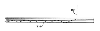
도 1과 도 2는, 본 발명의 LGSP(100)의 제1 실시예의 횡단면도를 나타낸다. 패널(100)은, 하나의 광-투입 스테이지(102)와 하나의 광 도파 스테이지(104)를 가지며, 이들은 모두 여하한 적합한 광 전송 물질로 만들어질 수 있다. 광-투입 스테이지(102)는, 그것의 입력면(108)에서 태양광(106)을 받아들이고, 그리고 그곳으로부터 태양광(106)은, 예를 들어, 일련의 반사판들(110)과 같은, 광학 부재들을 향해 가이드된다. 반사판들(110)은, 광 투입 스테이지(102)의 광 전송 물질과 구역들을 구성하는 물질(114) 사이의, 인터페이스들(112)에 의해 구획된다. 인터페이스들(112)이 충돌하는 태양광(106)에 대해 놓인 각도, 그리고 광-투입 스테이지(102)의 광 전송 물질의 굴절률의, 구역들의 물질(114)의 굴절률에 대한 비율은, 인터페이스들(112)에 충돌하는 태양광(106)이 내부 전반사를 일으키도록 선택된다. 일반적으로, 물질(114)은, 공기 또는 여하한 다른 적합한 기체이나, 그외의 여하한 다른 적합한 물질이 또한 물질(114)을 구성할 수 있다. 광-투입 스테이지(102)의 물질과 광 도파 스테이지(104)의 물질은, 예를 들어, 각종 폴리머 또는 아크릴 유리(acrylic glass), 예컨대, 광 스펙트럼(optical spectrum)의 가시부분(visible part)에 대해 약 1.49의 굴절률을 가지는, 폴리(메틸-메타크릴레이트) (PMMA)를 포함할 수 있다. 그외의 여하한 다른 적합한 물질이 또한 사용될 수 있다. 인터페이스들(112)이 충돌하는 태양광(106)에 대해 놓인 각도는, 인터페이스(112)의 표면 법선(surface normal)으로부터 측정된 바와 같이, 임계각(critical angle) 내지 90°의 범위 내에 있다(예를 들어, PMMA-공기 인터페이스에 있어서, 이 각도는 대체적으로 약 42.5°와 90°사이로 이루어진다).1 and 2 show a cross-sectional view of a first embodiment of
반사판들(110)은 포물선형 반사판들의 형상을 가지게 되나, 그들은 여하한 다른 적합한 형상일 수 있다. 만약 반사판들 사이의 간격이 "A"이고, 그리고 좌표계(system of coordinates)의 원점(origin)이 광 출력공(116)이면, 상응하는 포물선(parabola)의 하나의 예시적인 등식은 y = (1/2A)x2-1/4 이다. 도 1에 나타나 있는 바와 같이, 각 반사판(110)은, 태양광(106)을 광 출력공(116)에 초점 맞추어줌으로써 태양광(106)을 각각의 광 출력공(116)을 향해 보낸다. 도 2는, 동일한 반사판(110)에 의한 태양광(106)의 초점 맞춤을 보여준다. 그렇게 초점 맞추어진 태양광(106)은, 태양광(106)이 전파되는 방향인 벽(118)을 포함하는 광 도파 스테이지(104)에 들어간다. 이 벽(118)은, 광 도파 스테이지(104)의 광 전송 물질과 벽(118)의 다른 측면에 놓인 물질(122) 사이에 제1 면(120)을 가진다. 인터페이스(118)가 수평면에 대해 놓일 수 있는 각도는, 1 - 5°의 범위 내에 있으나, 여하한 다른 적합한 각도가 또한 만들어질 수 있다. 광 출력공들(116)로부터 나오는 태양광(106)에 대한 벽(118)의 배향, 그리고 광 도파 스테이지(104)의 광 전송 물질의 굴절률의, 물질(122)의 굴절률에 대한 비율은, 제1 면(120)에 충돌하는 태양광(106)이 내부 전반사를 일으키도록 선택된다. 물질(122)은, 공기 또는 여하한 다른 적합한 기체일 수 있으나; 광 도파 스테이지(104)의 것보다 더 낮은 굴절률을 가지는 여하한 다른 물질이 또한 물질(122)을 구성할 수 있다. 광-투입 스테이지(102)의 물질과 광 도파 스테이지(104)의 물질에 있어서, 그들은, 예를 들어, 각종 폴리머 또는 아크릴 유리, 예컨대, PMMA를 포함할 수 있다. 여하한 다른 적합한 물질이 또한 사용될 수 있다.The
일단 태양광(106)이 제1 면(120)에서 내부 전반사되면, 그것은 광 도파 스테이지(104)에서 일련의 반사 부재들(reflecting elements)(124)을 향해 전파되며, 이 반사 부재들은 태양광(106)이 다시 한번 내부 전반사를 일으키는 제1 면(120)을 향해 태양광(106)을 반사한다. 도 3에 나타나 있는 바와 같이, 각 반사 부재(124)는, 광 도파 스테이지(104)의 광 전송 물질, 그리고 구역들(114)의 것과 동일한 물질일 수 있는, 구역(128)을 구성하는 물질 사이의 인터페이스(126)에 의해 구획된다. 제1 면(120)으로부터 나오는 태양광(106)에 대한 반사 부재들(124)의 배향, 그리고 광 도파 스테이지(104)의 광 전송 물질의 굴절률의, 물질(128)의 굴절률에 대한 비율은, 반사 부재들(124)에 충돌하는 태양광(106)이 내부 전반사를 일으키도록 선택된다. 그러나, 반사 부재들(124), 제1 면(120) 및 반사판들(110)의 기능(function)은 내부 전반사를 기초로 할 필요가 없으며, 예를 들어, 적합한 종류의 반사경을 포함할 수 있다.Once the
도 1 - 도 3의 예시적인 실시예들에 나타나 있는 바와 같이, 각 반사 부재(124)는 평면이며, 그리고 입력면(108)에 대해 비-평행 각도(예를 들어, 1 - 5°)로 놓여 있다. 또한, 각 반사 부재(124)는, 입력면(108)으로부터 실질적으로 동일한 거리에 놓여 있으며, 그리고 제1 면(120)과 실질적으로 평행이다. 따라서, 광 도파 스테이지(104)는, 도 1 - 도 3에 나타나 있는 바와 같이, 일반적으로 쐐기의 형상을 가지며, 이것은 광 도파 스테이지(104)에 입력되는 태양광(106)을 광 출력공들(116)을 통해 쐐기가 넓어지는 방향 [다운스트림(downstream) 방향이라 함]으로 전파하는 역할을 한다. 그러므로, 광 도파 스테이지(104)는, 제1 면(120)에서의 그리고 반사 부재들(124)에서의 여러 번의 연속적인 내부 전반사들 후에, 태양광(106)이 [여하한 적합한 종류의 SEC (도시되지 않음)가 태양광(106)에 의해 운반된 에너지를 수집하도록(harvest) 구성될 수 있는] 측벽(132)의 일부분인 출력면(130) (도 1과 도 2)에 도달하도록 구성된다.Each
도 1과 도 2에는, 측벽(132)이 입력면(108)에 대해 직교하지 않는 것으로 나타나 있으나; 측벽(132)은 입력면(108)으로부터 여하한 적합한 각도로 놓일 수 있다. 또한, 이 분야의 통상의 지식을 가진 자들이 알 수 있듯이, LGSP(100)는, 여하한 적합한 수의 반사 부재들(124)과 여하한 적합한 수의 광 출력공들(116)을 가질 수 있다.In Figures 1 and 2, the
도 3은, 각 반사 부재(114)가 벽(118)과 평행하는 실시예의 것을 나타낸다. 이 실시예에서, 입사각은 태양광의 광선(106)이 다운스트림 방향으로 전파됨에 따라 변함없이 일정하다.Figure 3 shows an embodiment in which each
도 4는, 제1 면(120)(도 1)으로부터 나오고 그리고 광-투입 스테이지(102)를 향해 전파되는 태양광(106)이, 하나의 반사 부재(124)로부터 반사되고 그리고 광 출력공(116)에 충돌하지 않게, 반사 부재들(124)이 구성될 수 있음을 보여준다.Figure 4 shows that
도 5는, 벽(118)과 반사 부재들(124) 사이의 각도가 평행하지 않지만 다운스트림 방향으로 벌어져 있는(open), 본 발명의 다른 실시예를 보여준다. 이 실시예에서, 태양광(106)이 광 도파 스테이지(104)에 가두어진 채로 있게 될 것을 알 수 있다. 도 6은, 벽(118)과 반사 부재들 사이의 각도가 다운스트림 방향으로 가까와지는(close) 실시예를 보여준다. 이 실시예에서, 태양광(106)이 결국 광 도파 스테이지(104)로부터 빠져나가는 것을 볼 수 있다.Figure 5 shows another embodiment of the present invention in which the angle between the
도 7은, 도 1에 나타나 있는 횡단면을 가질 수 있는 LGSP(100)의 사시도를 보여준다. 도 7의 LGSP(100)는, 태양광(106)을 측벽(132)에 집광시킨다. 도 7의 LGSP(100)의 실시예는, 반사판들(110)이 모두 평행하는 선들을 따라 놓여 있기 때문에 선형 형상을 가진다고 할 수 있다.Fig. 7 shows a perspective view of
도 7의 LGSP(100)의 성능은, X 축과 Y 축에 의해 구획되는 평면에서 태양광(106)의 입사각의 변화들에 대하여 실질적으로 변하지 않는다. 각각 30°와 45°에서 입력면(108)에 입사하는 광선들(134 및 136)이, 광-투입 스테이지(102)에 의해 광 도파 스테이지(104)로 보내지고, 그리고 광 도파 스테이지(104)에서 출력면(130)을 향해 다운스트림으로 전파되는, 도 8A - 도 8C에 이러한 불변성(invariance)이 나타나 있다. X-Y 평면에서 입사각에 대한 이러한 불변성 때문에, 도 7의 LGSP(100)는, 태양광(106)을 패널의 엣지에, 바꿔 말하면, 출력면(130)에, 효과적으로 집광시키기 위해 여하한 적합한 단일 축 태양 추적장치(single axis sun tracker)와 함께 사용될 수 있다. 이 분야의 통상의 지식을 가진 자가 알 수 있듯이, 단일 축 추적장치는, LGSP(100)에 의해 포획되는 태양광의 양을 최대화하기 위해 패널이 태양과 지속적인 정렬을 이루게 한다.The performance of the
도 9는, 도 1에 나타나 있는 횡단면을 가질 수 있는 다른 LGSP(100)의 사시도를 보여준다. 도 9의 LGSP(100)는, 대체적으로 원반(138)으로 형상화되며, 그리 고 태양광을 원반(138)의 허브 구역(hub region)에 형성된 내벽(140)에 집광시키는데, 이 내벽(140)은, 여하한 적합한 방식을 통해, 여하한 적합한 SEC에 광학적으로 결합될 수 있는, 출력면(142)의 역할을 한다. 태양광(106)이 SEC에 결합될 수 있는 방법의 예들이 아래에 더 설명되어 있다. 도 9의 LGSP(100)의 실시예는, 반사판들(110)이 동심원들 위에 놓여 있기 때문에 회전 형상을 가지는 것으로 설명될 수 있다. SEC들은, 예를 들어, 광기전력 검출기들(photovoltaic detectors), 태양 전지들, 입사 태양광을 모으고 그것을 조명 기구들에 사용하기 위해 광섬유들(fiber-optics)에 의해 빌딩 내부로 전송하는 광 섬유 수집기들(fiber-optic collectors), 그리고 예를 들어, 물을 가열하기 위한 집열기들(thermal collectors), 또는 그들의 조합체(combination)를 포함한다.Figure 9 shows a perspective view of another
도 9의 LGSP(100)는, 여하한 바람직한 장착 브래킷(mounting bracket) 또는 구조(도시되지 않음)에 적합하게 만들기 위해, 도 10에 나타나 있는 바와 같이 사각형 패널들(rectangular panes)로, 또는 도 11에 나타나 있는 바와 같이, 모난 슬라이스들(angular slices)로, 또는 여하한 다른 적합한 형상의 조각으로 절단할 수 있다.The
이 분야의 통상의 지식을 가진 자가 알 수 있듯이, 도 7 - 도 11에 나타나 있는 LGSP들(100)은, 예를 들어, 단일 축 추적 시스템들 및 이중 축 추적 시스템들과 같은, 여하한 적합한 종류의 태양 추적 시스템들에 설치될 수 있다. 도 7 - 도 11의 LGSP들(100)에 있어서, 집광도(concentration)와 태양광 수용각(angular sunlight acceptance) 사이에 설계 타협들(design tradeoffs)이 이루어질 수 있으 며, 그렇게 함으로써 필요한 정렬상태(required alignment)와 추적 정밀도(tracking precision)가 결정된다. 도 7의 LGSP(100)는, 예를 들어, 20 - 50 suns의 집광도들을 달성할 수 있으며, 약 1°의 단일 축 태양 추적을 필요로 할 수 있다. 도 10의 LGSP(100)는, 예를 들어, 약 500 - 1000 suns의 집광도를 달성할 수 있으며, 약 1°의 이중 축 추적을 필요로 할 수 있다. 도 10의 LGSP(100)의 중앙에 더 큰 허브 구역을 가지는 것은, 바꿔 말하면, LGSP(100)의 중앙에 더 큰 개구부(opening)를 가지는 것은, 허브 구역이 더 작은 경우 보다 더 적은 집광도를 가져올 것이며, 덜 정밀한 추적을 필요로 할 것이다.As one of ordinary skill in the art will appreciate, the
이 분야의 통상의 지식을 가진 자가 알 수 있듯이, 광 출력공(116)의 너비(width)의, 반사판(110)의 가로 스판(horizontal span)에 대한 비율이, 집광도를 결정한다. 만약 이 비율이 광 출력공(116)이 극도로 빈틈 없을(tight) 정도로 아주 작게 만들어지면, 집광도가 매우 높게 이루어질 수 있으나, 수용각(angular acceptance)은 아주 작을 것이다. 광 출력공이 빈틈 없이 작을수록, 면(118)과 면(108) 사이의 각도가, 예를 들어, 1°와 같이, 더 작게 만들어지기 때문에, 116의 너비와 110의 가로 스판 사이의 비율이 또한 제1 면(120)의 각도에 영향을 줄 것이다. 이것은 이어서 더 작은 측벽(132), 그리고 이 때문에 더 작은 SEC를 가져올 수 있다.As one of ordinary skill in the art will appreciate, the ratio of the width of the
제작 목적들을 위해, 예를 들어, 도 7과 도 10의, LGSP(100)를 위한, 광-투입 스테이지(102)와 광 도파 스테이지(104)가, 도 12에 나타나 있는 바와 같은 뚜렷한 레이어들(distinct layers)을 형성할 수 있다. 이것은 광-투입 스테이지(102)에 출구면(exit face)(144)을 그리고 광 도파 스테이지(104)에 진입면(injection face)(146)을 만든다. 출구면(144)과 진입면(146)은 평행하거나 평탄할 필요가 없다. 출구면(144)과 진입면(146)은, 광 출력공(116)의 일부이다.For fabrication purposes, for example, the light-
도 13은, 본 발명의 LGSP의 다른 실시예의 횡단면을 보여준다. 도 13의 실시예에서, 태양광(106)은, 광 출력공(output optical aperture)(116)에서 광 도파 스테이지(104)로 입력되기 전에, 제1 반사판(148), 제2 반사판(150) 및 제3 반사판(152)에 부딪쳤다가 튀어나온다(bounce). 제1, 제2 및 제3 반사판들은 광학 부재들이며, 예를 들어, 평면, 포물면, 쌍곡면, 타원형면 및 원형면과 같은 여하한 적합한 형상을 가질 수 있다.Figure 13 shows a cross-sectional view of another embodiment of the LGSP of the present invention. 13, the
또한, 예를 들어, 렌즈들, 프레넬(Fresnel) 렌즈들, 포물선형 트로프들(parabolic troughs), 카세그레인 광학계들, 윈스턴 콘들(Winston cones) 및 테이퍼진 프리즘들(tapered prisms)과 같은 여하한 적합한 광학 부재들이 또한 광-투입 스테이지(102)에 포함될 수 있다. 광학 부재들은, 태양광(106)을 광 출력공들(116)로 광 도파 스테이지의 일반적인 다운스트림 방향으로 전할 수 있기만 하면 된다. 광 도파 스테이지(104)는, 광-투입 스테이지(102)의 실시예와는 별도로 독립적일 수 있는데, 바꿔 말하면, 동일한 광 도파 스테이지(104)가 광-투입 스테이지(102)의 다른 실시예들을 위해 사용될 수 있다.It should also be appreciated that any suitable suitable lens can be used, such as, for example, lenses, Fresnel lenses, parabolic troughs, Cassegrain optics, Winston cones and tapered prisms. Optical elements may also be included in the light-injecting
도 14는, 카세그테인 광학 설계(Cassegrain optic design)를 가지는 광-투입 스테이지(102)의 실시예를 보여준다. 이 실시예에서, 포물선형 제1 반사경(154)과 쌍곡선형 제2 반사경(156)이 태양광(106)을 초점 맞추어 평탄 반사판(158)으로 보내기 위해 사용된다. 태양광(106)은, 반사판(158)에서 반사되어, 광-투입 스테이지(102)의 광 출력공의 역할을 하는 진입면(160)에서 광 도파 스테이지(104)에 들어간다. 도 14의 실시예는, 선형 또는 회전 형상 LGSP에 사용될 수 있다. 도 14의 카세그레인 광학계들은, 평탄 반사판(158) 위 뿐만 아니라 제1 및 제2 반사경들(각각, 154 및 156) 위의 반사면들(mirrored surfaces)을 필요로 한다.Figure 14 shows an embodiment of a light-injecting
도 15는, 광-투입 스테이지(102)의 광 전송 물질과, 공기 또는 여하한 다른 적합한 기체일 수 있는 물질(166) [그러나, 여하한 다른 적합한 물질이 또한 물질(166)을 구성할 수 있음] 사이에 있는 인터페이스들(164A 및 164B)에 의해 구획된 일련의 윈스턴 콘들(Winston cones)(162)을 가지는 광-투입 스테이지(102)를 보여준다. 충돌하는 태양광(106)에 대한 인터페이스들(164)의 형상, 그리고 광-투입 스테이지(102)의 광 전송 물질의 굴절률의, 물질(166)의 굴절률에 대한 비율은, 인터페이스들(164)에 충돌하는 태양광(106)이 내부 전반사를 일으키도록 선택된다. 인터페이스들(164A 및 164B)에 의해 구획되는 일정한 콘(원뿔체)(162)에 있어서, 인터페이스(164A)에 충돌하는 태양광(106)은, 반사판(168)을 향해 반사되는데, 이 반사판(168)은 이번에는 태양광(106)을 광 출력공(116)으로 보낸다. 인터페이스(164B)에 충돌하는 태양광(106)에 있어서, 그것은, 그것이 반사되는 인터페이스(164B)에 따라, 광 출력공(116)으로, 또는 광 출력공(116)을 향해 그것을 반사할 반사판(168)으로, 직접 반사될 것이다. 반사판(168)에 직접 충돌하는 태양광(106)에 있어서, 그것은 또한 광 출력공(116)으로 보내진다. 광 출력공(116)을 통해 광 도파 스테이지(104)에 들어간 후에, 태양광(106)은, 제1 면(120) 또는 반사 부재(124)의 어느 하나에, 어느 쪽이든, 충돌할 수 있고, 태양광(106)은 내부 전반사를 일으키며, 그리고 다운스트림 방향으로 전파된다. 반사판(168)은, 예를 들어, 둥근 형상(rounded geometry)과 같은 여하한 적합한 형상을 가질 수 있으며, 여하한 적합한 종류의 반사 코팅(mirrored coating)을 포함할 수 있다. 도 15의 광-투입 스테이지(102)는, 선형 또는 회전 형상 LGSP에 사용될 수 있다. 도 15의 광-투입 레이어(102)는, 그것의 비교적 넓은 태양광 수용각(sunlight acceptance angle)으로 인해 비-추적(non-tracking) 태양 전지판들에 사용될 수 있다.15 depicts a schematic cross-sectional view of a light emitting device according to another embodiment of the present invention, in which a light transmitting material of the light-injecting
상술한 실시예들에서, 광 도파 스테이지의 광 출력공에 인접한 광 도파 스테이지(104)의 높이를 감소시킴으로써 집광도를 증가시킬 수 있다. 상기 실시예들에 설명되어 있는 바와 같이, 광 도파 스테이지(104)는 태양광의 내부 전반사에 의해 태양광(106)을 전파한다. 일반적으로, 만약 광 도파 스테이지가 도 6에 나타나 있는 바와 같이 다운스트림 방향으로 테이퍼지거나(taper) 수렴되면, 태양광은 광 도파 스테이지로부터 빠져나올 것이다. 그러나, 이러한 제한은 광 도파 스테이지 내의 마지막 반사에는 적용되지 않으며, 이 시점에서는, 태양광이 광 도파 스테이지(104)를 빠져나올 것이기 때문이다. SEC에 의해 태양광을 수집하기 바로 직전에, 태양광은, 그것이 광 도파 스테이지의 광 출력공에 도달하는 것을 조건으로 하여, 여하한 적합한 각도로 반사될 수 있다. SEC가 태양광을 수집할 것이기 때문에, 빛의 입사각은 덜 중요하며, 그에 따라, 빛은 수집되기 바로 직전에 더 꽉 죄어지거나(pinched), 더 집광될 수 있다. 이러한 방식으로 달성가능한 부가적인 집광은, 광 도파 스테이지(104) 내에 태양광(106)의 각도 스프레드(angular spread)에 좌우되며, 광 가이드 레이어(light guide layer) 내에 평행하는 빛이 많을수록 더 큰 집광을 달성할 수 있다. 일반적인 실시예들에서, 여분의 집광(extra concentration)은, 예를 들어, 1.5 배(times)와 2 배 사이의 범위 내에 있을 수 있다.In the above-described embodiments, the degree of condensation can be increased by reducing the height of the
이러한 여분의 집광을 부가하는 가장 간단한 방법은, SEC에 가까운 광-가이드 레이어를 테이퍼지게 하는 것이다. 집광에 유효한 테이퍼는, 비-축 포물면(off-axis paraboloid)이며, 그 하나의 예가 도 16에 도면 부호 170으로 나타나 있는, 윈스턴 콘(Winston Cone)이다. 그러나, 그러한 윈스턴 콘(170)을 포함하는 것은, 위로부터 윈스턴 콘에 입사하는 빛이 실질적으로 포획되지 않기 때문에, LGSP(100에 [빛을 포획하지 않고 빛을 SEC로 전송하지 않는, 태양광에 노출된 LGSP 면으로 정의되는] 데드 스페이스(dead space)를 도입시킨다. 그러한 데드 스페이스는, 태양 에너지를 유용한 에너지로 변환시키기 위한 공간의 사용에 있어서 전체 시스템 효율의 감소들을 가져온다.The simplest way to add this extra condensation is to taper the light-guide layer close to the SEC. The taper that is effective for focusing is a non-axis paraboloid, one example of which is Winston Cone, shown at 170 in FIG. However, including such a Winston con (170) does not require that the light incident on the Winston cone from above is substantially captured, so that the LGSP 100 (which does not capture light and does not transmit light to SEC, Dead space defined by the exposed LGSP plane. Such dead space leads to reductions in overall system efficiency in the use of space to convert solar energy into useful energy.
여분의 집광과 데드 스페이스 사이의 절충은, 도 17에 나타나 있는 하프 윈스턴 콘(half Winston Cone)(172)을 사용함으로써 달성될 수 있다. 도 18에 나타나 있는, 다른 대안적인, 평탄 마면 테이퍼(flat faceted taper)(174)가, 윈스턴 콘의 효과에 근접하기 위해 사용될 수 있다. 그러나, 평탄 마면 테이퍼는, 윈스턴 콘이 제공할 수 있는 것과 동일한 부가적인 집광을 제공하지 않는다. 이러한 사실에도 불구하고, 평탄한 부재들이 곡선 모양의 부재들 보다 제조하기가 더 쉽기 때문에, 도 18에 나타나 있는 접근법(approach)이 흥미로울 수 있다.The trade-off between extra light condensation and dead space can be achieved by using the
상술한 집광 증가는, 개별적인 광학 부재, [광 전송 물질로 만들어지고, 광 도파 스테이지와 SEC (도시되지 않음) 사이에 고정될 수 있는] 핀치(pinch)를 사용하여 달성될 수 있다. 이러한 핀치는 도 18에 도면 부호 176으로 나타나 있다. 만약 핀치(176)의 굴절률이 광 도파 스테이지의 것보다 더 크면, 더 부가적인 집광을 얻을 수 있다. 광 도파 스테이지와 핀치(176) 사이의 인터페이스(180)에서 태양광 편향(sunlight deflection)이 일어나기 때문에 그리고 높은 굴절률 물질 [핀치(176)]과의 임계각(critical angle)이 더 낮기 때문에, 부가적인 집광이 일어난다.The above-described increase in condensation can be achieved by using a separate optical member, a pinch (made of a light-transmitting material, which can be fixed between the optical waveguide stage and SEC (not shown)). This pinch is indicated at 176 in FIG. If the refractive index of the
예를 들어, 핀치(176)와 같은 광학 부재를 광 도파 스테이지와 SEC 사이에 두는 것의 이점은, 그것이 SEC에서의 열 축적에 대항하여 광 도파 스테이지를 단열시킬 수 있다는 점이다. 만약 최악조건하의 운용(worst-case operation) 중에 광 도파 스테이지를 구성하는 물질이 견딜 수 있는 것보다 SEC가 더 뜨겁게 되면, 위와 같은 이점이 중요하게 된다.For example, an advantage of placing an optical member, such as a
본 발명의 LGSP(100)의 다른 실시예가 도 19에 나타나 있다. 이 실시예는, 광 도파 스테이지(104)로 하여금 광 도파 스테이지(104)에 의해 구획된 일련의 벽들(182)에 고정된 일련의 SEC들에 태양광을 제공하게 한다. 이 분야의 통상의 지식을 가진 자가 알 수 있듯이, 복수의 벽들(182)을 사용하는 것은 더 얇은 광 도파 스테이지(104)를 가능하게 한다.Another embodiment of the
광-투입 스테이지(102)의 입력면(108)과 광 도파 스테이지(104)의 제1 면(120)을 보호하기 위해, 도 20에 나타나 있는 피복층(184)이 입력면에 그리고/또는 제1 면에 부착될(applied) 수 있다. 피복층은 광-투입 스테이지의 굴절률 보다 더 낮고 그리고 광 도파 스테이지의 것보다 더 낮은 굴절률을 가질 수 있다. 더욱이, 피복층(184)은 또한 통상적으로 공기 또는 기체가 차지하게 되는 LGSP(100) 내의 모든 공간들에 부착될 수 있다.In order to protect the
그러한 피복층(184)을 가지는 이점은, LGSP의 완전한 상태(integrity)를 보호할 수 있다는 점이다. 그러한 피복층(184)이 존재함으로써, LGSP의 피복의 외면(outer surface)이 오염되거나 긁혀도 LGSP의 기능을 저하시키지 않을 수 있다. 피복층(184)은, 예를 들어, 불화 에틸렌 프로필렌(fluorinated ethylene propylene)과 같은 여하한 적합한 물질로 만들어질 수 있다. 이 분야의 통상의 지식을 가진 자가 알 수 있듯이, 피복층의 두께는 비교적 얇아도 효과적일 수 있다.The advantage of having such a
위에 설명한 LGSP의 실시예들은 크기가 조절가능하다(scalable). 바꿔 말하면, 그들의 치수들은, 광학계들이 간섭 효과들(interference effects)이 커질 만큼 광학계들이 작아지지 않는 것을 조건으로 하여, 광학계들의 기능발휘(functioning)에 영향을 주지 않고서 일반적인 요인(common factor)에 의해 모두 바뀔 수 있다. 그러한 간섭 효과들은, 엇갈리게 배열된(staggered) 광학 부재들간의 간격이 광 파장들(optical wavelengths)에 비교될 수 있을 정도(scale)일 때 중요하게 될 수 있다. 태양 스펙트럼의 가장 강력한(energetic) 파장 부분은, 0.2 - 3 미크론(microns) 사이이다. 따라서, 홈들(apertures)의 크기 뿐만 아니라 광학 부재들과 홈들의 스태거링 피리어드(staggering period)는, 간섭 효과들을 완화시키기 위해 3 미크론 보다 더 크게 유지될 수 있다.The embodiments of LGSP described above are scalable. In other words, their dimensions can be determined by common factors, without affecting the functioning of the optical systems, provided that the optical systems are not so small that the interference effects are large. Can be changed. Such interference effects can be significant when the spacing between staggered optical elements is comparable to optical wavelengths. The most energetic wavelength part of the solar spectrum is between 0.2 and 3 microns. Thus, the staggering period of the optical elements and grooves as well as the size of the apertures can be kept larger than 3 microns to mitigate interference effects.
최소한의 재료를 사용하고 원가를 낮게 유지하기 위해, 광학 부재들을 작게 만들어서 LGSP들의 두께를 최소화하고 최소한의 재료로 최대 커버리지(maximum area coverage)를 가능하게 하는 것이 바람직하다. 광 도파 스테이지(광-가이드 레이어)의 두께는, 태양광을 수집하도록 구성된 SEC들의 크기[예를 들어, 광기전력 전지 스트립들(strips)의 크기]에 의해 주로 제한될 것이다. 광기전력 전지 스트립들의 경우에, 그들의 크기는, 더 크거나 더 작은 광기전력 전지들도 마찬가지로 잘 작동할 수 있기는 하나, 예를 들어, 1 밀리미터 내지 1 센티미터로 변화할 수 있다. 다른 한편으로는, 광-투입 스테이지 (투입 레이어)가 간섭 효과들과 제작 방법들이 이를 허용하는 만큼 얇게 만들어질 수 있다.In order to use minimal materials and keep costs low, it is desirable to make the optical elements small to minimize the thickness of LGSPs and to allow maximum area coverage with minimal material. The thickness of the light-guiding stage (light-guide layer) will be largely limited by the size of the SECs configured to collect sunlight (e.g., the size of the photovoltaic cell strips). In the case of photovoltaic cell strips, their size may vary from, for example, 1 millimeter to 1 centimeter, although larger or smaller photovoltaic cells may work equally well. On the other hand, the light-injecting stage (input layer) can be made as thin as interference effects and fabrication methods allow it.
본 발명의 LGSP들은, 사출 성형(injection molding), 압축 성형(compression molding), 사출-압축 성형과 같은 몰딩 기술들(molding techniques)에 의해 또는 여하한 다른 적합한 방법들에 의해 제작될 수 있다. 일반적으로 말하면, 몰딩에 의해 만들어진 부품들(parts)은 언더컷들(undercuts)을 가질 수 없으며, 따라서, 상술한 전체 광-가이드 전지판들을 통상적인 몰딩을 사용하여 한번에 몰딩하는 것이 불가능하다. 그러나, LGSP는, 개별적으로 몰딩될(molded) 수 있는 섹션들로 나누어 제조할 수 있다. 제조를 위한 목적으로 LGSP를 섹션화하기 위한 두 가지 예시적인 접근법들을 아래에서 설명한다.The LGSPs of the present invention can be produced by molding techniques such as injection molding, compression molding, injection-compression molding, or any other suitable methods. Generally speaking, parts made by molding can not have undercuts, and therefore it is impossible to mold all the light-guide panel plates described above at once using conventional molding. However, the LGSP can be manufactured by dividing into sections that can be individually molded. Two exemplary approaches for sectioning the LGSP for manufacturing purposes are described below.
첫 번째 접근법은, LGSP의 얇은 세로형 섹션들, 또는 슬라이스들을 제조하여, 그들을 도 21에 도시되어 있는 바와 같이 나란히 조립하는 것이다. 그러한 패널의 개개의 슬라이스들(190)은, 외부 파지구(external bracing) (도시되지 않음) 에 의해 함께 고정하거나, 또는 접착하거나(glue) 다른 방법으로 접합할(bond) 수 있다. 이러한 첫 번째 접근법 (슬라이스 이용법)은, 선형 형상 LGSP들에 적합하다.The first approach is to fabricate thin vertical sections, or slices, of LGSP and to assemble them side by side as shown in Fig. The
두 번째 접근법은, 그 하나를 다른 것의 위에 적층하여 LGSP를 만들 수 있는 가로형 슬래브들(horizontal slabs)을 제조하는 것이다. 이러한 패널들은, 조립(framing)과 인클로저들(enclosures: 외장)을 거의 필요로 하지 않는, 자기지지형일 수 있으며, 그리고 접착(gluing) 또는 접합(bonding)이 필요하지 않게 구성될 수 있다. 슬래브들은, 앞서 설명된 기능성 레이어들(functional layers) [광-투입입 스테이지와 광 도파 스테이지]을 구성하고; 그러나, 그러한 기능성 레이어는 여하한 수의 슬래브들로 만들어질 수 있다.The second approach is to fabricate horizontal slabs that can be stacked one on top of the other to form the LGSP. These panels can be self-supporting, requiring little framing and enclosures, and can be configured without the need for gluing or bonding. The slabs constitute the functional layers described above (light-input and output stage and light-wave stage); However, such a functional layer can be made of any number of slabs.
도 22A - 도 22D는, LGSP(100)를 언더컷들 없이 세 개의 시트들(sheets)로 나누는 방법을 보여준다. 상부의 두 개의 시트들(192 및 194)은 함께 작용하여 투입 레이어 [광-투입 스테이지(102)]를 만들고, 하부 시트(196)는, 광-가이드 레이어 [광 도파 스테이지(104)]를 형성한다. 도 22A - 도 22D에 나타나 있는 실시예는, 도 13에 나타나 있는 것과 유사하다. 상부 슬래브(192)에서, 태양광(106)은, 내부 전반사 (TIR)에 의해 포물선형 반사판으로부터 반사되고, 그 다음에 상부 슬래브(192)를 빠져나와서, 중간 슬래브(194)로 들어가며, 그 다음에 중간 슬래브(194)를 빠져나와서, 광-가이드 레이어 [광 도파 스테이지(104)]의 역할을 하는, 하부 슬래브(196)로 들어가기 전에 TIR에 의해 두 개의 평탄 마면들(flat facets)로부터 반사된다.22A-22D show how to divide the
도 23A - 도 23C는, LGSP(100)가 위와 달리 두 개의 슬래브들(198 및 200)로나뉠 수 있음을 보여준다. 투입 레이어와 광-가이드 레이어가 각기 하나의 슬래브로, 즉, 슬래브들(198 및 200)로 각각 만들어지는 것이다. 도 24A에 나타나 있는 바와 같이, 태양광(106)은 포물면(parabolic surface)(202)으로부터 내부 전반사되고, 그 다음에 광-가이드 레이어 (광 도파 스테이지)의 진입면(206)과 마주치기 전에 평탄 마면 [출구면(exit surface)](204)을 통해 공기속으로 빠져나간다. 투입 레이어 슬래브의 출구면(204)에서의 편향은, 포물선형 반사판의 초점(focal point)을 변경하며; 그것은 초점을 약간 업스트림 방향으로(upstream) 이동시키며, 그에 따라 광 가이드 레이어의 홈들(apertures)의 업스트림 방향으로의 이동을 필요로 한다. 초점이 약간 이동하는 것에는 이점이 있는데, 그 포물선형 반사판 면들의 촘촘한 패킹(tight packing)을 그들 사이에 데드-스페이스가 거의 없이 가능하게 한다는 점이다. 그러나, 태양광을 집광시키기 위해 반사만이 아닌 편향을 사용할 때의 단점은, 그것을 실제로 만들었을 때 단일 축 태양광 추적에 의해서는 최적으로 기능하지 않을 것이라는 점이다. 그러므로, 도 24A의 2-슬래브 접근법은 회전 형상 LGSP에 아주 적합하다. 이러한 사실은, 이 실시예가, 최적의 성능을 위해, 어느 경우에도 2 축 추적(two axis tracking)을 필요로 하기 때문이다. 평탄 마면에 의한 초점의 이동은, 포커싱 포물선형 광학계(focusing parabolic optic)에 얼마간의 작은 비점 수차(some small astigmatism)를 도입시킨다. 이것은 태양광(106)을 초점에서 약간 분산시키며, 달성가능한 집광을, 약간 제한한다. 포물선(parabola)을 약간 기울임(tilting)으로써 비점 수차를 얼마간 보상하는 것이 가능하다. 만약 평탄 마면(204)이 수직면으로부터 시계 방향과 반대 방향으로 2°기울어지면, 포물선형 반사판(110)을 수직면으로부터 시계 방향으로 5°기울임으로써 비점 수차를 얼마간 보상할 수 있다. 도 24B는, 도 24A의 것과 유사하나, 대신에 진입면(206)에 의해 형성된 돌출부(207)와 접해 있는 3차 곡면(cubic surface)(203)을 구비한, 광-가이드 태양 전지판의 다른 실시예를 보여준다.23A-23C show that the
도 24C는, 도 24B의 광-투입 스테이지의 주기적 유닛(periodic unit), 즉, 3차원 반사면(cubic reflector)(203), 평탄 마면(204), 진입면(206) 및 돌출부(207)를 포함하여 구성되는 유닛에 대한 예시적인 치수들을 보여준다. 길이들은 미크론으로 나타나 있으며, 3차원 반사면(203)의 등식은, y = -1.049388x + 9.1781775x10-4x2 + 1.19193x10-7x3 이다.24C shows a periodic unit of the light-input stage of Fig. 24B, namely a three-dimensional
도 25A - 도 25C는, LGSP(100)를 두 개의 슬래브들(208 및 210)로 나누는 또 다른 예를 보여주며, 이러한 분할은, 도 24A의 실시예의 최적이 못되는 단일 축 추적과 관련된 한계를 개선하고, 태양광을 집광하기 위해 편향을 사용하지 않는 선형 형상 LGSP의 제조를 가능하게 한다. 도 26에 나타나 있는 바와 같이, 태양광(106)은 포물선형 반사면(parabolic reflector)(212)으로부터 내부 전반사되나, 이 실시예에서 태양광(106)은 포물선형 반사면(212)의 초점에 중심을 둔 원의 호(arc)인 출구면(214)에서 투입 레이어 슬래브를 빠져 나온다. 포물선형 반사면의 초점에 모이는 태양광 광선들은 각기 호형 출구면(arc exit face)과 실질적으로 직각으로 마주치며, 그래서 편향이 일어나지 않는다.25A-25C show yet another example of dividing the
상술한 슬래브들 모두는, LGSP들로 조립될 때 그들 사이의 정렬을 용이하게 하는 어셈블리 피처들(조립 형상부들: assembly features)을 갖도록 몰딩될 수 있다. 조립 형상부들은 광학적 성능(optical performance)에 최소한도로 지장을 주거나 전혀 지장을 주지 않을 수 있다. 구체적으로, 본 발명의 LGSP의 실시예들은, 업스트림 공들(upstream apertures)의 후부(backside)가 포물선형 반사판들의 하부에 기대어지도록 설계될 수 있으며; 이것은 도 25C에 나타나 있는 실시예를 가지는, 실시예이다. 다른 조립 형상부들은, 광-가이드 레이어의 표면 위에 분산되어 있고,광 도파 스테이지(104)에 대하여 적소에 포물선형 반사판들을 고정시키는, 작은너브들(nubs)을 포함할 수 있다. 슬래브들 사이의 공간은 먼지와 수분이 실질적으로 없어야 한다. 슬래브들은, 실리콘(silicone) 또는 여하한 다른 적합한 물질을 사용하여, 또는 개스킷(gasket) 또는 여하한 다른 적합한 시일(seal)을 사용하여 서로 실링될(sealed) 수 있다. 수분을 흡수하기 위해 슬래브들 사이에 소량의 건조제가 부가될 수 있다. LGSP를 깨끗하게 유지하고 그리고 건축물(architecture)과 어울리는 색상을 가능하게 하기 위해 더스트 재킷(dust jacket) 또는 풀 엔벨로프(full envelope)가 LGSP에 부가될 수 있다.All of the slabs described above can be molded with assembly features that facilitate alignment between them when assembled with LGSPs. The assembled features may at least or not hinder optical performance. Specifically, embodiments of the LGSP of the present invention can be designed such that the backside of upstream apertures leans against the bottom of the parabolic reflectors; This is an embodiment with the embodiment shown in Figure 25C. Other assemblies may include small nubs dispersed over the surface of the light-guide layer and fixing the parabolic reflectors in place relative to the
단일 축 추적 태양 전지판 시스템(216)이 도 27에 도시되어 있다. 태양 전지판 시스템(216)은, 상술한 2-슬래브 접근법을 사용하여 제조된 LGSP들(100)을 사용할 수 있으며, 축(218) 주위에 경사지게 조립될 수 있다. LGSP들(100)은, 각 측면이 125 밀리미터인 정사각형들로 만들어질 수 있다. 광-가이드 레이어 (광-투입 스테이지)는, 높이가 3 mm인 광기전력 전지들에 빛을 집광시키기 위해 하프 윈스턴 콘(half Winston Cone)을 사용할 수 있다. 그러한 시스템의 광학적 집광도(optical concentration)는 대략 30 suns이다.A single axis tracking
시스템(216)은, 알루미늄 또는 여하한 다른 적합한 물질로 만들어질 수 있는, 히트 싱크(220)의 양측에 두 개의 평행하는 열을 이루어 배열되고, 그들이 히트 싱크(220)에 결합되는 패널들의 내부 엣지를 향해 빛을 집광시키는 방식으로 배열된, 여러 개의, 예컨대, 10개의 태양 전지판들(100)을 사용하여 만들어진다. 광기전력 전지들은 광 패널들(optical panels)(100)과 히트 싱크(220) 사이에 배치된다.The
태양 전지판들(100)은, 예를 들어, 도 28에 도시된 리브들(222)에 의해 정렬될 수 있다. 이 리브들은, 기계가공된(machined) 알루미늄 또는 여하한 다른 물질이 사용될 수 있기는 하나, 사출-성형 폴리머로 만들어질 수 있다. 리브들(222)은 패널들(100)을 히트 싱크(220)에 대해 기계적으로 고정하며, 그리고, 조립을 용이하게 하기 위해 리브들(222)과 히트 싱크(220) 모두에 조립형상부들(features)이 포함될 수 있다. 그러한 형상부들 [예를 들어, 오목부(recess)(224)] 그리고 리브(222)와 히트 싱크(220)에 대한 상세한 사항들이 도 28과 도 29에 각각 나타나 있다. 리브들(222)은, 기계적 파스너들(fasteners), 접착제들, 또는 여하한 다른 적합한 수단을 사용하여 히트 싱크에 대해 고정될 수 있다.The
이 히트 싱크(220)는, (1) 광기전력 전지들로부터 열을 소산시키는데 도움을 주고, (2) LGSP들(100)을 위한 단단한 지지축을 만드는, 두 가지 기능들을 제공할 수 있다. 패널들의 중량은 히트 싱크(220)의 양측에서 균형이 유지되며, 그리고 히트 싱크(220)는 패널이 외부 지지 프레임(external supporting frame)에 결합되는 장소이다. 열을 소산시키는데 도움을 주기 위해, 그리고 도 29에 나타나 있는 바와 같이, 히트 싱크(220)는, 두 개의 사출성형된 알루미늄 레일들(rails)(228) 사이에 결합된, 접어 겹쳐진 알루미늄 조각으로 만들어진 핀들(fins)(226)을 가질 수 있다. 이 핀들(fins)은, 두 개의 레일들에 결합되며, 히트 싱크(220)에 수직 공기 채널들(vertical air channels)(230)을 만든다. 핀들(fins)과 두 개의 레일들 사이의 결합(bond)은, 경납땜(brazing), 에폭시(epoxy), 스웨이징(swaging)에 의해 또는 여하한 다른 수단에 의해 만들어질 수 있다. 이러한 개방 히트-싱크(open heat-sink) 실시예는, 뜨거운 공기가 히트-싱크(220)로부터 솟아오를 수 있고 냉각제 공기가 아래로부터 히트-싱크(220)로 들어갈 수 있기 때문에 열이 자연 대류(natural convection)에 의해 소산되게(dissipated) 한다.The
시스템(216)에 사용되는 광기전력 전지들은 여하한 크기, 즉, 125 밀리미터 × 125 밀리미터의 크기일 수 있으며, 여하한 높이의, 예컨대, 이 실시예에 사용하기 위한 3 mm 높이의 스트립들로 절단될 수 있다. 광기전력 전지들은 통상적인 방식으로 캡슐화될(encapsulated) 수 있다. 예를 들어, 그들은 직렬로 함께 납땜된 다음에 에틸렌 비닐 아세테이트(ethylene vinyl acetate: EVA) 또는 여하한 다른 적합한 물질로 캡슐화될 수 있다. 이와 달리, 광기전력 전지들의 전기적 연결부들(electrical connections)은, 광기전력 전지들을 열 전도성 유전체 기 재(thermally conductive dielectric substrate)의 패턴 회로(patterned circuit)에 납땜, 부착 또는 접합시킴으로써 이루어질 수 있다. "The Bergquist Company of Chanhassen Minnesota"에 의해 판매되는 것들과 같은 절연 금속 기재들(insulated metal substrates: IMS들)이 적합할 것이다. 도 30은, 광기전력 전지(234)에 납땜된 IMS 기재(232)를 보여주며, 납땜 레이어(solder layer)는 235로 나타나 있다. IMS(232)는, 에폭시 또는 접착제에 의해, 또는 여하한 다른 적합한 수단에 의해 알루미늄 히트 싱크(220)에 결합될 수 있다.The photovoltaic cells used in the
전형적인 IMS(232)는, 알루미늄 또는 구리 베이스(base)에 접합되는 폴리머-절연 층 상부에 구리의 전기 패터닝(electrical patterning)을 가진다. 베이스를 사용하지 않고(forgo), 전기 패터닝 폴리머-절연 층(electrically patterned polymer-insulating layer)을 히트 싱크(220)에 바로 부착시키는 것이 가능하다. 이 공정은 오븐에서 열 경화에 의해 행해질 수 있다. 이러한 접근법의 하나의 장점은, 그것이 베이스 부재를 생략하여, 비용을 감소시킬 수 있다는 점이다. 광기전력 전지(234)는, 광기전력 전지(232)의 상부 커넥터(topside connector) (도시되지 않음)의 전체 길이(entire length)에 걸쳐 연결된 전도성 리본 또는 메쉬(conductive ribbon or mesh)를 통해 IMS(232)에 접합될 수 있다. 광기전력 전지(232)의 후부 커넥터는, 그 전체 길이 그리고/또는 표면에 걸쳐서 접합될 수도 있다. 길이가 길고 그리고 폭이 좁고 그리고 연약한 광기전력 전지들(232)을 위해, 상술된 결합 방법을 사용하는 것은, PC 전지들로 하여금 그들의 기능성(functionality)을 잃지 않고서 또는 전력 생산에 실질적으로 영향을 주지 않고서 섹션들로 나뉠 수 있게 한다.A
광기전력 전지들은, 수분으로부터 보호하여 부식을 피하기 위해 캡슐화될 수 있다. 이것은, 예를 들어, 에틸렌 비닐 아세테이트 (EVA)와 같은 여하한 적합한 밀 봉재(encapsulant)를 사용하여 할 수 있다. 그러나, EVA는, 열 경화를 필요로 하며, 그래서, 실링을 필요로 하는 부품들은 오븐에 넣을 필요가 있다. 다른 접근법은, 실온에서 제자리에서 경화하는, 밀봉재를 사용하는 것이다. "Dow Corning"의 "silicone Sylgard184"와 같은, 어떤 광학상 투명 접착제들(optically clear adhesives)은, 이 목적을 충족시킬 수 있고, 납땜 후에 광기전력 전지들의 상부에 얇은 레이어로 부어질 수 있다. 부가적인 이점으로서, 패널들이 실리콘(silicone)의 경화가 시작되기 전에 제자리에서 고정될 수 있다. 이것은, 패널들과 광기전력 전지들 사이의 공간을 실링하고, 그들 사이에 광학적 결합(optical bond)을 만든다. 광 패널들(optical panels)과 광기전력 전지들 사이의 광학적 결합은, 광 패널의 출구 엣지(exit edge)에서 프레넬 손실들(Fresnel losses)을 감소시킨다.Photovoltaic cells can be encapsulated to protect against moisture and to avoid corrosion. This can be done, for example, using any suitable encapsulant, such as ethylene vinyl acetate (EVA). However, EVA requires thermal curing, and so parts that require sealing need to be placed in an oven. Another approach is to use a sealant that cures in situ at room temperature. Some optically clear adhesives, such as "
LGSP들은, 태양광 발전 시스템(solar power system)을 만들기 위해 장착 프레임(mounting frame) 위에 배열될 수 있다. 히트 싱크들은 장착 프레임 위의 베어링들과 결합될 수 있으며, 그렇게 하면, 패널이 히트-싱크(220)에 의해 만들어진 축[도 27에서 축(218) 참조] 주위를 자유롭게 회전하게 한다. 히트 싱크(220)는, 히트 싱크(220)의 말단들에 결합된, 사출 성형 말단 캡들(injection molded end caps) (도 27, 236)에 의해 베어링들에 결합할 수 있다. 이러한 말단 캡들(236)은, 프레임 위의 베어링들에 대한 결합을 가능하게 하는 여하한 적합한 형상들을 가질 수 있다. 말단 캡들(236)은, 기계적으로, 에폭시들, 접착제들로, 접착제 테이프로, 또는 여하한 다른 적합한 수단을 통해, 히트-싱크에 결합될 수 있다. 히트-싱크(220)의 말단 캡들(236)은 또한 액튜에이터(actuator)로 하여금 LGSP들(100)의 회전을 제어하게 하는, 메커니즘(mechanism)에 결합된다. 예를 들어, 도 31에 나타나 있는 바와 같이, 3 바아 링크 장치들(three bar linkages)이, 선형 액튜에이터(240)에 의해 구동되는 단일 레일(single rail)(238)에 모든 모듈들을 결합시킬 수 있다. 이와 달리, 각 LGSP는, 선형 액튜에이터에 의해 다시 구동되는, 래크(rack)에 부착된 피니언 기어(pinion gear)를 가질 수 있다. 어느 시스템에서도, 단일 레일을 움직이는 단일 선형 액튜에이터가 모든 패널들이 일제히 기울어져서 정렬을 유지하도록 그들을 작동시킬 수 있다.The LGSPs can be arranged on a mounting frame to make a solar power system. The heat sinks can be mated with the bearings on the mounting frame so that the panel is free to rotate about the axis created by the heat-sink 220 (see
회전형상을 가지는 LGSP를 사용하여 완전 태양광 추적 태양 전지판 시스템(full sunlight tracking solar panel system)을 만들 수 있으며, 이것은 도 23A - 도 23C에 예시되어 있는 2-레이어 접근법을 사용하여 제작할 수 있다. 그러한 완전 추적 시스템들의 외관은, LGSP들이 중앙의 히트-싱크의 양측을 따라 배열될 수 있고, 리브들(ribs)에 의해 지지될 수 있다는 점에서, 단일 축 추적 시스템에 대해 위에 설명되어 있는 것들과 유사할 수 있다.The LGSP having a rotating configuration can be used to make a full sunlight tracking solar panel system, which can be fabricated using the two-layer approach illustrated in Figures 23A-23C. The appearance of such full tracking systems is that the LGSPs can be arranged along both sides of the central heat-sink and can be supported by ribs, Can be similar.
패널들의 바깥쪽 치수들은, 125 밀리미터 × 250 밀리미터일 수 있다. 태양광은, 도 32A와 도 32B에 나타나 있는 바와 같이 LGSP의 내부 엣지의 중앙에 있는 선(242)에 집광된다. 태양광은, 반원통형 면(half cylindrical facet)(244)에서 태양 전지판(100)을 빠져나와, 에어 갭(air gap)에 들어간다. 원칙적으로 얇은 광기전력 전지가 선(242)을 따라 놓여질 수 있기는 하나, 그러한 배열은 수용각(angular acceptance)을 제한할 것이다.The outside dimensions of the panels may be 125 millimeters by 250 millimeters. The sunlight is focused on a
실제로, 더 넓은 수용각은, 도 33A - 도 33C에 나타나 있는 바와 같이, 90°루프 프리즘(roof prism)(246)을 반원통형 면에 놓음으로써 달성된다. 이 루프 프리즘(246)은, 유리로 또는 여하한 다른 적합한 물질로 만들어질 수 있으며, 1.4 보다 큰 굴절률(index of refraction)을 가질 수 있다. 고 효율 광기전력 전지들, 예컨대, 삼중-접합(triple-junction) 전지들은, 실리콘 밀봉재 또는 다른 광 에폭시(optical epoxy)를 사용하여 루프 프리즘의 베이스(248)에 광학적으로 결합될(bonded optically) 수 있다. 도 33D - 도 33G는, 어떻게 사각형 광-가이드 태양 전지판(800)이, 각기 하나의 회전 형상과 하나의 상응하는 광 도파 스테이지 섹션(806 및 808)을 가지는, 두 개의 광-투입 스테이지 섹션들(802 및 804)을 사용하여 만들어질 수 있는지를 보여준다. 광-투입 스테이지(802)에 충돌하는 태양광은, 태양광을 면(810)에 전파하는 광 도파 스테이지(806)에 광학적으로 결합된다. 광-투입 스테이지(804)에 충돌하는 태양광에 있어서, 그것은 태양광을 면(812)에 전파하는, 광 도파 스테이지(808)에 결합된다. 면들(810 및 812)은 평탄한 면들일 수 있으며, 여하한 적합한 SEC들이 거기에 고정될 수 있다. 광 도파 스테이지들(806 및 808)로부터 빠져나오는 빛을 결합시키기 위해 프리즘을 사용하지 않음으로써, 프레넬 반사 손실들(Fresnel reflections losses)이 회피될 수 있다. 광 도파관들(806 및 808)은, 도 33E에 나타나 있는 것과 같은 하프-윈스턴 콘 프로파일들(half-Winston cone profiles)(816 및 818)을 가질 수 있다. 도 33F는, 광-가이드 태양 전지판(800)이 광-투입 스테이지들(802 및 804)을 광 도파 스테이지들(806 및 808)의 위에 놓음으로써 이들이 2-레이어 공정(two-layer process)에서 만들어질 수 있음을 보여준다. 도 33G는, 도 33E의 어셈블리의 분해 조립도를 보여준다. 광학계의 양 측면들로부터 태양광이 나온다고 가정하면, 히트 싱크들이 패널의 개개의 마주 보는 측면들에 놓일 수 있다. 도 33D의 이 패널이 커플링 프리즘(coupling prism)을 가지지 않기 때문에, 광 도파 스테이지들(806 및 808)의, 면(810 및 812)에 인접한 부분은, 예를 들어, 용융 실리카(fused silica)와 같은, 더 많은 열을 견디어낼 수 있는, 절연 물질로 만들어질 수 있고, 그 나머지는 PMMA로 만들어진다.In practice, a wider receiving angle is achieved by placing a 90 °
[반원통형 면(244)을 빠져나온 다음에 프리즘(246)에 의해 광기전력 전지로 보내지는 태양광에 대해] 도 33A - 도 33C과 관련하여 위에 설명되어 있는 배열(arrangement)은, 시스템에 프레넬 손실들을 가져오기는 하나, 그것은 또한 기체[공기, 또는 예를 들어 아르곤과 같은 여하한 다른 적합한 기체]의 층을 광기전력 전지와 직접 접촉하는 프리즘(246)과 LGSP 사이에 놓는다. 이러한 배열의 장점은, 그것이 광기전력 전지에 축적될 수 있는 열로부터 광학계들 (LGSP)을 보호한다는 점이다. 광기전력 전지는, 높은 집광 하에, 극도로 뜨겁게 될 수 있고, 아마도 120℃ 또는 그보다 더 높은 온도에 도달할 수 있으며, 이것은 만약 광 패널이 PMMA로 만들어졌다면 그것에 불리하게 작용할 것이다. 기체 층은, 광 패널을 절연시킬 수 있고, 그리고 광기전력 전지의 열 축적으로부터 광 패널을 보호할 수 있다.[For sunlight that is sent to the photovoltaic cell by the
앞서 언급한 바와 같이, 회전 형상을 사용하고 그리고 높은 태양광 집광도(high solar concentration)를 위해 설계된 LGSP들은, 태양의 완전 추적과 관련하여 사용될 때 더 우수한 성능을 제공하여, 태양 전지판의 입력면의 노말 벡터(normal vector)에 대해 +/-1°내로 평행하게 태양의 광선들을 유지한다. 완전 추적은, 여러 가지 방식으로 달성될 수 있으나, 2 방법들이 특히 이 시스템에 적합하다. As mentioned earlier, LGSPs, which are designed for use with a rotating configuration and for high solar concentration, provide better performance when used in conjunction with full tracking of the sun, And keeps the sun's rays parallel to +/- 1 ° to the normal vector. Full tracking can be achieved in many ways, but two methods are particularly suitable for this system.
LGSP들(100)이 제1 시리즈의 축들(250) 주위로 경사지도록 프레임(249)에 설치되어 있고, 축들(250)에 대해 실질적으로 직교하는 축(252) 주위로 프레임(249)이 경사질 수 있는, 첫 번째 완전 추적 방법이 도 34에 나타나 있다. 따라서, LGSP는 해가 떠 있는 동안 태양의 이동을 추적하기 위해 동-서로 회전할 수 있고, 프레임은 북-남으로 경사져서 태양의 계절적인 변화에 순응할 수 있다.The
더 낮은 프로파일(a lower profile)을 취하게 하는 두 번째 완전 추적 접근법이, 도 35와 도 36에 나타나 있다. LGSP들(100)은, 프레임들(254 또는 256)에 배열될 수 있으며, 축들(258 및 260) 주위로 각각 기울어질 수 있다. 또한, 프레임들(254 및 256)은, 축들(262 및 264) 주위로 각각 회전하도록 만들어질 수 있다.A second complete tracking approach, which takes a lower profile, is shown in Figures 35 and 36. The
도 37은, 도 15에 나타나 있는 바와 같은, 투입 레이어 [광-투입 스테이지(102)]에 윈스턴 콘들을 사용하는 LGSP의 변형(variant)을 보여준다. 선형 형상 실시예인, 도 37의 실시예는, 윈스턴 콘들 때문에 넓은 수용각을 가지므로, 비-추적 용도들에 아주 적합하다. 달성가능한 집광을 증진시키기 위해, 2개의 광 패널들 사이에 위치된 하나의 2면(bifacial) 광기전력 전지(266)를 사용하는 것이 가능하며; 이러한 실시예는 집광을 두 배로 만든다.FIG. 37 shows a variant of the LGSP using Winston cones for the input layer (light-input stage 102), as shown in FIG. The embodiment of Fig. 37, which is a linear shape embodiment, is well suited for non-tracking applications because of its wide acceptance angle due to Winston cones. In order to promote achievable condensation, it is possible to use a single bifacial
도 37의 LGSP(100)는, 각 광기전력 전지 스트립을 위한 태양 전지판을 만들기 보다는, 2 파트 스택(a two part stack)으로 만들어질 수 있고, 복수의 집광기 광학계들(concentrator optics)을 더 적은 수의 조각들로 그룹지어진 것인, 광 패 널들의 클러스터(cluster)를 만들 수 있다. 도 38은, 어떻게 클러스터 LGSP(268)가 4개의 광기전력 전지들(266)을 수용하도록 만들어질 수 있는지를 보여준다.The
광-가이드 레이어들 [광 도파 스테이지들(104)]을 구성하는 슬래브(270)는, 2면 광기전력 전지들(266)을 수용하기 위해 그것에 몰딩된(molded) 홈들(grooves)(272)을 가질 수 있다. 광기전력 전지들(266)은, 납땜된 다음에 홈에 놓이기 전에 캡슐화될 수 있거나, 또는 그들은 함께 납땜되어 회로를 만든 다음에 홈에 놓여지고, 투명(clear) 실리콘 또는 여하한 다른 광 에폭시와 같은 캐스트 인 플레이스 밀봉재(cast in place encapsulant)를 사용하여 제자리에서 캡슐화될 수 있다.The
복수의 클러스터 패널들을 함께 부착시켜 완전 태양 전지판 모듈을 만든다. LGSP들을 함께 결합시키기 위한 수많은 방법들이 존재한다. 그 하나의 방법은, 알루미늄 프레이밍 그릴(framing grill)을 사용하여 모든 패널들을 함께 결합시키는 것이다. 다른 방법은, 광 패널들을 정렬시키고 여하한 적합한 수단에 의해 유리 또는 여하한 다른 적합한 물질로 된 딱딱한 덮개(superstrate)에 접합시키는(bond) 것이다.A plurality of cluster panels are attached together to form a complete solar panel module. There are a number of ways to combine LGSPs together. One way to do this is to use an aluminum framing grill to join all the panels together. Another method is to bond the optical panels to a superstrate made of glass or any other suitable material by aligning and by any suitable means.
비-추적 LGSP(268)은, 도 37에 나타나 있는 바와 같이 광학계들의 횡단면에 180°의 수용각을 가지지 않는 것이 일반적일 것이다. LGSP(268)의 수광 콘(cone of acceptance)은 패널의 법선(normal)으로부터 +/-30°일 수 있으며, 이것은 하늘에서 태양의 위치의 계절적인 변화를 수용하기에 충분하다. 따라서, 비-추적 LGSP(168)는, 설치 위치의 위도에 맞는 기울기로 설치되어야 하며; 이것은 패널의 입력면에 대한 법선이 주야 평분점(equinox)에서 태양의 광선들과 평행하는 것을 보장할 것이다. 그러나, 이것은 비-추적 LGSP(268)의 설치 배열들(installation configurations)을 제한한다. 사실상, LGSP(268)는, 그들의 수광 콘(cone of acceptance)이 북반구 지역들에 대해 도 39에 나타나 있는 바와 같이 법선으로부터 경사지게 설계될 수 있다. 실제로, 유한한 수의 비-추적 LGSP들(268) 시리즈(series)는, 어떤 설치 배열도 수용할 수 있게 설계될 수 있다.It will be common that the
가능한 한 비용 효율적으로 본 발명의 LGSP를 제조하기 위해, 롤-투-롤 연속 캐스팅(roll-to-roll continuous casting) 또는 엠보싱(embossing)이 광-투입 스테이지 광학계들을 필름들(films)로 제조하는데 사용될 수 있다. 상기 태양 전지판들 모두가 언더컷들을 가지지 않는 슬래브들의 더미(stack)로 구성되기 때문에, 롤-투-롤 제조 방법들을 사용하는 것이 가능하다. 쐐기-형상 광-가이드 레이어 (광 도파 스테이지)는 개별적으로 만들어질 수 있으며, 광-투입 스테이지는 적층 공정(lamination process) 또는 여하한 다른 적합한 공정을 사용하여 광 도파 스테이지에 부착될 수 있다.In order to make the LGSP of the present invention as cost-effective as possible, roll-to-roll continuous casting or embossing is used to fabricate the light-injecting stage optical systems as films Can be used. Since all of the solar panels are comprised of a stack of slabs with no undercuts, it is possible to use roll-to-roll manufacturing methods. The wedge-shaped optical-guide layers (optical waveguide stages) can be made individually and the light-injecting stages can be attached to the optical waveguide stage using a lamination process or any other suitable process.
이 분야의 통상의 지식을 가진 자가 알 수 있듯이, 본 발명의 LGSP의 광-투입 레이어(102)는 또한 상술한 바로 그 포커싱 TIR 인터페이스들(focusing TIR interfaces) 대신에 여하한 적합한 종류의 렌즈들을 광학 부재들로서 사용할 수 있다. 도 40은, 태양광(106)을 광 도파 스테이지(104)에 초점 맞추고 광학적으로 결합시키는 일련의 렌즈들(274)을 가지는 LGSP(100)를 보여준다.As one of ordinary skill in the art will appreciate, the light-injected
본 발명의 LGSP의 다른 실시예가 도 41A, 도 41B, 그리고 도 42A - 도 42D에 나타나 있다. LGSP(300)는, 하나의 투입 레이어 [광-투입 스테이지(302)]와 하나의 광-가이드 레이어 [광 도파 스테이지(304)]를 가진다. 광-투입 스테이지(302)는, 하나의 편향기 섹션(deflector section)(306)과 반사판 섹션들(312) 형태의 광학 부재들을 가진다. 편향기 섹션(306)은, 충돌하는 태양광(106)을 이중-화살표(308)로 표시된 방향들 중의 한 방향으로 또는 양 방향으로 편향시킨다. 편향된 태양광은, 일련의 포커싱 테이퍼진 광 채널들(focusing tapered light channels)로 형상화되는, 반사판 섹션들(312)인, 광학 부재들을 향해 보내진다. 테이퍼진 광 채널들은, 광 도파 스테이지(304)를 형성하는 일련의 도파관들(314)에, 일련의 광 출력공들(313)을 통해 광학적으로 결합된다.Another embodiment of the LGSP of the present invention is shown in Figures 41A, 41B, and 42A-42D. The
편향기 섹션(306)은, 볼륨 위상 홀로그램 (Volume Phase Hologram: VPH) 형태의 광 다이렉팅 레이어(optical directing layer)를 포함할 수 있다. 두 개의 간섭성 UV 광원들(coherent UV light sources) 사이의 간섭을 사용하여, VPH 홀로그램에 여하한 적합한 방식으로 광선 줄무늬들(fringes)이 형성된다. 광선 줄무늬 간격과 각도는, 하나 또는 그보다 많은 회절 모드들(modes of diffraction)이 태양 전지판(300)의 평면의 45도 이내에 있을 수 있게 설계될 수 있다. 도 42A는, 그러한 VPH(309)가 어떻게 작동하는 지에 대한 하나의 예를 보여준다. 그 결과로 얻은 편향이 도 42B 내지 도 42D에 예시되어 있다.The
편향기 섹션(306)은 또한 예를 들어, 프리즘들과 같은 평탄 마면 광학계들(flat faceted optics)과 같은, 비-간섭 광학계들(non-interference optics)을 사용하여 만들어질 수도 있다. 예를 들어, 그들 사이에 작은 에어 갭을 가지는 맞 물림 방식(interlocking manner)으로 배열된 60° 프리즘들의 하나의 어레이는, 패널의 평면에 입사하는 빛을 두 방향들로 나눌 것이다. 이러한 2-방향 편향은, 빛을 태양 전지판(300)의 두 개의 마주 보는 엣지들에 축적되게 할 것이다. 그러한 다이렉팅 광학계들(directing optics)이 도 43에 나타나 있다.The
광 도파 스테이지(304)는 선형 형상을 가지며, 그리고 그들 각각의 테이퍼진 광 채널들 [반사판 섹션(312)]로부터 빛을 수신하고 그리고 내부 전반사에 의해 빛을 포획하는, 복수의 도파관들(314)을 가질 수 있다. 도파관들(314)은 지연 라인들(delay lines)의 역할을 하는데, 그것에 의해, 빛이 위로부터 광 출력공들(313)에 들어가서, 얼마간의 거리를 이동한 다음에 광 출력공들(313)을 통해 상부 밖으로 빠져나갈 수 있다. 가능한 채널의 실시예가 도 42A - 도 42C에 나타나 있다. 테이퍼진 광 채널 [반사판 섹션(312)]에 들어가는 광은, 도파관(314)를 구획하는, 원통형 섹션으로 들어가기 전에, 제1 포물선형 섹션(316)으로부터, 그 다음에 평탄한 면(318)으로부터 그리고 제2 포물선형 섹션(320)으로부터 반사된다. 광은, 도파관(314) 내를, 빠져나오기 전에, 얼마간의 거리를 나선형 식으로 이동할 수 있다. 만약 도파관(314)의 길이가 포획된 광선들의 평균 이동 거리(mean travel distance) 보다 더 작다면, 도파관(314)에 결합된 광은 그것이 여하한 적합한 SEC에 의해 수집될 수 있는, 채널의 말단으로부터 집광되어 나올 것이다. 하나의 예로서, 만약 광 도파 스테이지(104)의 높이가 1 cm 이고 그리고 도파관들(314)의 길이가 150 cm 이면, LGSP(300)에 입사하는 빛의 75%가 SEC에 의한 수집을 위해 도파관의 두 말단들에 도달할 것이다. 만약 빛이 LGSP(300)에 균일하게 입사하면, 광은 도파관 채널의 두 말단들 사이에 균일하게 분포될 것이다.The
LGSP(300)는 도파관들(314)과 테이퍼진 광 채널들(312)을 얼마든지 포함할 수 있으며, 각 도파관(314)는 각각의 테이퍼진 광 채널(312)과 하나의 유닛(unit)을 형성할 수 있다. 테이퍼진 광 채널(312)과 그들 각각의 도파관들(314)에 의해 만들어진 유닛들은 몰딩(molding)에 의해 만들어질 수 있다.The
LGSP(300)에서, 각 도파관(314)는 하나의 출력면(315)을 가지며, 출력면(315)의 전체 합(sum)은, 광 도파 스테이지(304)의 전체 출력면을 형성한다. 여하한 적합한 SEC가 태양광(106)을 수집하기 위해 복수의 광 출력공들(315)의 출력부에 놓일 수 있다.In
테이퍼진 광 채널들/도파관의 다른 형상들이 사용될 수 있다. 예를 들어, 도 44A - 도 44C는, 거기에 형성된 복수의 도파관들(326)을 가지는 테이퍼진 광 채널(322)을 보여주며, 여기서, 테이퍼진 광 채널의 너비가 감소함에 따라 도파관의 직경이 감소한다. 도파관들의 수직으로 엇갈림(staggering)은, 둘 또는 그보다 많은 채널들로 하여금 그들 사이에 데드 스페이스(dead space)가 거의 없도록 나란히 밀접하게 위치되게 한다.Other shapes of tapered optical channels / waveguides may be used. For example, Figs. 44A-44C show a tapered
앞서 설명된 히트 싱크(220)는, 단일 축 추적 시스템들과 완전 추적 고 집광기 시스템들(full tracking high concentrator systems)과 함께 사용되어, 과량의 열을 SEC (예를 들어, 광기전력 전지들)로부터 주변 공기로 발산할 수 있다. 그러나, 과량의 열은 대신에 물을 가열하기 위해 사용될 수 있다. 이러한 기능은 도 45A와 도 45B에 나타나 있는 히트 싱크(400)로 성취될 수 있다. 히트 싱크(400)는 알루미늄 또는 여하한 다른 적합한 물질로 만들어질 수 있다. 과량의 열을 공기 중으로 발산하는 핀들을 특징으로 하는 히트 싱크(220)와는 달리, 히트 싱크(400)는, SEC들에서 발생되는 과량의 열을 빼내는 물을 흐르게 하기 위한 하나 또는 그보다 많은 채널들(402)을 가진다.The previously described
도 46에 나타나 있는 바와 같이, 말단 캡들(end caps)(403)이 히트 싱크(400)에 부착될 수 있고, LGSP들을 베어링들(bearings)을 통해 장착 프레임에 고정시키는 이중 목적을 충족시킬 수 있으며, 그들은 또한 열 교환기 (도시되지 않음)로의 유입구와 유출구들의 역할을 한다. 물은, 하나의 말단 캡에 하나의 유입구를 그리고 다른 한쪽의 말단 캡에 하나의 유출구를 가지는, 히트 싱크(400)를 통해 일직선으로 흐를 수 있거나, 또는 그것은 동일한 말단-캡을 통해 히트 싱크(400)의 안과 밖으로 흐를 수 있는데, 상기 마주 보는 말단 캡은 u-벤드(u-bend)의 역할을 한다. 이 실시예는, 확대된(extended) 시스템에서 많은 모듈들 사이의 호스 배열(hose routing)을 단순화시킬 수 있다. 압출물(extrusion)에서 채널들의 수는, 물 그리고 히트 싱크(400)의 알루미늄 사이에 더 큰 접촉 표면적(larger surface area of contact)을 가지도록 증가될 수 있다. 히트 싱크(400)를 통한 물 흐름의 레이트(rate of water flow)가, SEC들의 온도를 제어하기 위해 사용될 수 있고, LGSP들을 그들의 작동 온도 범위내로 유지하기 위해 사용될 수 있다. 호스들(406)을 통해 상호연결된 히트 싱크들(400)을 사용하는 시스템이 도 46에 나타나 있다. 이 분야의 통상의 지식을 가진 자가 알 수 있듯이, 물이 아닌 열 교환 유체(heat exchange fluid)가 도 46의 시스템에 사용될 수 있다.As shown in Figure 46,
본 발명의 LGSP에 의해 포획된 태양광은, 광기전력 전지들을 사용하지 않는 태양 열 시스템에 사용될 수 있다. 그러한 태양 열 시스템(500)의 하나의 예가 도 47에 나타나 있다. 시스템(500)은, 그것의 가장 바깥의 투명 튜브(its outermost tube transparent)를 가지는, 이중 벽 튜브(double walled tube)(502)를 사용할 수 있다. 아르곤과 같은, 절연 기체가, 내부 튜브를 외부 튜브와 분리시킬 것이다. 내부 튜브는 입사하는 태양광을 흡수하기 위해 검은 색일 수 있다. 중앙 튜브를 통해 물, 오일, 또는 여하한 다른 적합한 액체와 같은 열 흡수 액체가 흐른다.The sunlight captured by the LGSP of the present invention can be used in solar thermal systems that do not use photovoltaic cells. One example of such a
튜브(502)는, 상술한 실시예들에서 히트 싱크들에 의해 앞서 차지된 위치에 놓인다. 집광된 태양광은, 투명한 외부 튜브와 절연 기체 층을 통과하여, 내부 튜브에 의해 흡수된다. 이것은 내부 튜브내의 액체를 가열시킨다. 유체 운반 튜브들(fluid carrying tubes)은 광학계들이 그들 주위를 회전하는 동안 적당한 위치에 고정된 채로 남아 있을 수 있다.The
실리콘 온 글래스(silicone on glass)로 알려져 있는 기술을 사용하여 본 발명의 LGSP의 몇몇 작은 광학 구조들을 제조하는 것이 가능하다. "Dow"의 SylgardTM 184 와 유사한, 얇은 투명 실리콘 러버(rubber)가 유리 기재 위에 필요한 형상들로 만들어진다. 유리 기재 없이 독자적으로 실리콘을 몰딩하는 것이 또한 가능하다.It is possible to manufacture several small optical structures of the LGSP of the present invention using a technique known as silicone on glass. A thin transparent silicone rubber, similar to the "Dow"
유리하게도, 본 발명의 LGSP는, 열 팽창 또는 수축에 대해 비교적 영향을 받지 않는다. 이것은 태양 전지판들의 모든 광학적 구성요소들이 동일하거나, 만일 동일하지 않다면 유사한 물질들로 만들어지기 때문에 가능하다. 이 때문에, 그들은 동일한 정도(degree)로 팽창할 것이며, 그리고 광학 부재의 기능은 크게 변화하지 않을 것이다. 특히, 반사판들(110)이 팽창함에 따라, 도파 섹션(104) 또한 팽창할 것이다. 유닛이 온도 변화로 팽창하고 수축함에 따라, 이것은 도 1의 110으로부터 반사되어 116에 초점 맞추어지는 빛(106)에 대해 동일한 초점을 유지한다.Advantageously, the LGSP of the present invention is relatively unaffected by thermal expansion or contraction. This is possible because all the optical components of the solar panels are made of the same or, if not identical, similar materials. For this reason, they will expand to the same degree, and the function of the optical member will not change significantly. In particular, as
단일 축 추적에 있어서, 패널은 입사하는 태양광과 하나의 평면으로 정렬을 유지하기 위해 기울어진다. 광학계들의 상부에, 빛을 사전에 조정하는, 광학 장치(optical device)를 부가하여, 광학계들에 입사하는 빛을 정렬시키기 위해 입사하는 빛의 각도를 변경하는 것이 또한 가능하다. 그러한 사전 조정 광학계들(preconditioning optics)은, 이동 반사경들, 프리즘들, 또는 전기-광학계들을 사용할 수 있다.In single axis tracking, the panel is tilted to maintain alignment with one plane with incident sunlight. On top of the optical systems it is also possible to add an optical device, which pre-adjusts the light, to change the angle of the incident light in order to align the light incident on the optical systems. Such preconditioning optics may use moving mirrors, prisms, or electro-optic systems.
추적은, 단일 축 추적 패널, 또는 비-추적 패널을 가끔씩 기울여줌으로써 수동으로(manually) 수행될 수 있다. 수동-추적 패널은, 몇 주마다 한번씩 손으로 약간 재정렬될 필요만이 있도록 충분히 넓은 수용각, 말하자면, 예를 들어, 횡단면에서 + 또는 - 5 도의 수용각을 가지는 것일 것이다. 전자 정렬 센서들(electronic alignment sensors)은 정렬에 도움을 줄 수 있으나, 액튜에이터들은 필요하지 않을 것이다.Tracking can be performed manually, by occasionally tilting a single-axis tracking panel or a non-tracking panel. The manual-tracking panel will have a sufficiently wide acceptance angle, say, say, + or -5 degrees in cross-section, so that it needs to be slightly reordered by hand every few weeks. Electronic alignment sensors can help with alignment, but actuators will not be needed.
다른 메커니즘을 사용하는 LGSP가 굴절률 그레디언트(gradient index of refraction)를 가지는 패널을 사용하여 만들어질 수 있다. 굴절률 그레디언트(refractive index gradient)는, 패널에 입사하는 빛이 다운스트림 방향을 향해 편향되도록, LGSP의 다운스트림 방향으로 증가한다. 만약 이 그레디언트가 TIR이 패널의 하부 면에서 일어날 만큼의 편향을 일으키기에 충분하다면, 빛이 포획되어, 도 48에 나타나 있는 바와 같이 패널의 엣지로 아래로 보내지게 될 것이다. 그레디언트가 더 작아서 만일 빛이 패널의 하부 면을 빠져나오면, 반사경이 첫 번째 반사를 위해 필요할 수 있으며, 그리고 패널을 통해 상부 면으로 다시 위로 이동하는 동안 추가 편향이 상부 면 위에서의 입사각을 TIR이 일어나기에 충분하도록 증가시킬 것이다. 이것은 도 49에 나타나 있다.LGSPs using other mechanisms can be made using panels with a gradient index of refraction. The refractive index gradient increases in the downstream direction of the LGSP such that the light incident on the panel is deflected toward the downstream direction. If this gradient is sufficient to cause the TIR to produce enough deflection to occur on the bottom surface of the panel, the light will be captured and sent down to the edge of the panel as shown in FIG. If the gradient is smaller so that the light exits the lower surface of the panel, a reflector may be needed for the first reflection, and additional deflection will cause the TIR to rise above the top surface while moving back up through the panel to the top surface . This is shown in FIG.
도 50A와 도 50B는, 도 33D의 광-가이드 태양 전지판(800)과 같은 광-가이드 태양 전지판들이 어떻게 함께 그룹지어질 수 있는지를 보여준다. 광-가이드 태양 전지판들(800)은, 두 개의 수직으로 배향된 알루미늄 히트 싱크들(900) 사이에 놓여서 광-가이드 태양 전지판들(800)의 선형 어셈블리(902)를 형성할 수 있다. 광-가이드 태양 전지판들(800)의 더 큰 그룹들은, 선형 어셈블리들(902)을 함께 결합시킴으로써 조립될 수 있다.Figures 50A and 50B show how light-guide solar panels, such as the light-guide
본 발명은, 유전체 패널 또는 다른 투명 패널 내부에 빛을 포획하기 위해 LGSP를 사용하고, 그리고 SEC에 의한 수집을 위해 패널 엣지들 중의 하나로 빛을 전파하는, 태양 에너지 시스템의 발명이다. 이것은, 모듈의 엣지에서 그 두께가, SEC의, 예를 들어, 광기전력 전지의, 높이에 필적하는, 아주 얇은 모듈들을 가능하게 하여, CPV 시스템들과 같은 종래의 태양 에너지 시스템들에 태생적인 깊이 요건들(depth requirements)을 제거한다. LGSP에 부딪히는 광은, 방향이 바뀌고, 그리고 SEC가 빛을 수신하는 패널의 엣지들 중의 하나를 통해 빛이 패널을 빠져나오도록 내부에 포획된다.The present invention is an invention of a solar energy system that uses LGSP to capture light inside a dielectric panel or other transparent panel and propagates the light to one of the panel edges for collection by SEC. This enables very thin modules whose thickness at the edge of the module, comparable to the height of the SEC, for example a photovoltaic cell, to provide depths inherent in conventional solar energy systems such as CPV systems Remove the depth requirements. The light impinging on the LGSP is redirected and captured internally through one of the edges of the panel where the SEC receives light, such that light exits the panel.
LGSP들은, 모듈들을 만들기 위해 클러스터들로 결합될 수 있다. LGSP 광학계들은, 충분히(largely) 자기지지형이도록 구조적으로 설계될 수 있으며, 이것은 그들이 그들의 형상 및 배향을 유지하기 위해 외부 인클로저(external enclosure)를 필요로 하지 않음을 의미한다. 풀 인클로저(full enclosure)가 실시예에 부가될 수 있다. 아래에 설명될 바와 같이, 재료 사용과 비용을 최소화하기 위해, LGSP 모듈들은 최소한의 축-및-리브 구조(axle-and-rib configuration)에 의해 지지될 수 있다.LGSPs can be combined into clusters to create modules. LGSP optical systems can be structurally designed to be largely self-supporting, meaning that they do not require an external enclosure to maintain their shape and orientation. A full enclosure may be added to the embodiment. As will be described below, in order to minimize material use and cost, LGSP modules can be supported by a minimum of axle-and-rib configuration.
집광된 태양광은, 광기전력 전지들로 전기를 만들어내는 것이 아닌 목적을 위해 활용될 수 있다. 하나의 대안적인 용도는 부재(element)를 가열하는 것이다. 모듈들은 또한 전기를 발생시키면서 동시에 물을 가열하도록 구성될 수 있다. 집광된 빛을 광 섬유 또는 다른 광-가이드와 결합시켜서, 그것을 어떤 다른 용도를 위한 다른 위치로, 예컨대, 태양광 조명을 제공하기 위한 조명 기구로, 전파하는 것이 또한 가능하다. 또한, 본 발명의 LGSP 광학계들은, 예를 들어, 램프들과 조명장치(lighting)를 포함하는 다른 용도들에서 광학계들의 두께를 감소시키기 위해 사용될 수 있다. 첨부된 도면들과 함께 본 발명의 특정 실시예들에 대한 다음의 설명을 검토함에 따라 본 발명의 다른 측면들과 용도들이 이 분야의 통상의 지식을 가진 자들에게 명백하게 될 것이다.Condensed sunlight can be used for purposes other than creating electricity with photovoltaic cells. One alternative application is to heat the element. The modules can also be configured to simultaneously generate electricity and heat the water. It is also possible to combine the condensed light with an optical fiber or other light-guide and propagate it to another location for some other use, for example, a luminaire for providing solar light illumination. Further, the LGSP optical systems of the present invention can be used to reduce the thickness of the optical systems in other applications including, for example, lamps and lighting. Other aspects and uses of the invention will become apparent to those skilled in the art upon review of the following description of specific embodiments of the invention in conjunction with the accompanying drawings.
전술한 설명에는, 해설의 목적을 위해, 매우 많은 세부사항들이 본 발명의 실시예들의 완전한 이해를 제공하기 위해 기술되어 있다. 그러나, 이러한 특정한 세부사항들이 본 발명을 실시하기 위해 필수적인 것은 아님을 이 분야의 통상의 지 식을 가진 자에게 명백할 것이다. 다른 경우들에는, 잘 알려진 전기 구조물들(electrical structures)과 회로들이 본 발명을 애매하게 하지 않기 위해 블록 다이어그램 형태(block diagram form)로 나타나 있다. 예를 들어, 특정한 세부사항들은 본 명세서에 설명되어 있는 본 발명의 실시예들이 소프트웨어 루틴(software routine), 하드웨어 회로(hardware circuit), 펌웨어(firmware), 또는 그 조합(combination)으로 구현되는지의 여부에 관하여는 규정되어 있지 않다.In the foregoing description, for purposes of explanation, numerous details are set forth in order to provide a thorough understanding of embodiments of the present invention. It will be apparent, however, to one of ordinary skill in the art that these specific details are not required to practice the present invention. In other instances, well-known electrical structures and circuits are shown in block diagram form in order not to obscure the present invention. For example, specific details are set forth such as how the embodiments of the invention described herein may be implemented in a software routine, a hardware circuit, a firmware, or a combination thereof Is not specified.
본 발명의 상술한 실시예들은 단지 예시들인 것으로 의도된 것이다. 이 분야의 통상의 지식을 가진 자들에 의해, 별도로 첨부된 특허청구범위에 의해서만 정의되는, 본 발명의 범위를 벗어나지 않고서 특정 실시예들에 대한 변경, 변형 및 변화가 이루어질 수 있다.The above-described embodiments of the present invention are intended to be illustrative only. Modifications, changes and variations may be made, by those skilled in the art, to specific embodiments without departing from the scope of the invention, which is defined solely by the claims appended hereto.
Claims (44)
Applications Claiming Priority (7)
| Application Number | Priority Date | Filing Date | Title |
|---|---|---|---|
| US91520707P | 2007-05-01 | 2007-05-01 | |
| US60/915,207 | 2007-05-01 | ||
| US94274507P | 2007-06-08 | 2007-06-08 | |
| US60/942,745 | 2007-06-08 | ||
| US95177507P | 2007-07-25 | 2007-07-25 | |
| US60/951,775 | 2007-07-25 | ||
| PCT/CA2008/000831 WO2008131561A1 (en) | 2007-05-01 | 2008-05-01 | Light-guide solar panel and method of fabrication thereof |
Publications (2)
| Publication Number | Publication Date |
|---|---|
| KR20100017477A KR20100017477A (en) | 2010-02-16 |
| KR101487896B1 true KR101487896B1 (en) | 2015-01-29 |
Family
ID=39925147
Family Applications (1)
| Application Number | Title | Priority Date | Filing Date |
|---|---|---|---|
| KR1020097024905A KR101487896B1 (en) | 2007-05-01 | 2008-05-01 | Light-guide solar panel and method of fabrication thereof |
Country Status (10)
| Country | Link |
|---|---|
| US (6) | US8152339B2 (en) |
| EP (4) | EP2153475B1 (en) |
| JP (2) | JP5837746B2 (en) |
| KR (1) | KR101487896B1 (en) |
| CN (2) | CN101681949B (en) |
| AU (1) | AU2008243623B2 (en) |
| CA (2) | CA2685108C (en) |
| ES (1) | ES2642209T3 (en) |
| IL (1) | IL201786A (en) |
| WO (2) | WO2008131566A1 (en) |
Families Citing this family (192)
| Publication number | Priority date | Publication date | Assignee | Title |
|---|---|---|---|---|
| EP2102912A2 (en) * | 2006-12-13 | 2009-09-23 | Pythagoras Solar Inc. | Solar radiation collector |
| US9337373B2 (en) | 2007-05-01 | 2016-05-10 | Morgan Solar Inc. | Light-guide solar module, method of fabrication thereof, and panel made therefrom |
| EP2153475B1 (en) | 2007-05-01 | 2017-07-12 | Morgan Solar Inc. | Light-guide solar panel and method of fabrication thereof |
| US9040808B2 (en) | 2007-05-01 | 2015-05-26 | Morgan Solar Inc. | Light-guide solar panel and method of fabrication thereof |
| US20110308611A1 (en) * | 2010-03-19 | 2011-12-22 | Morgan Solar Inc. | Solar-light concentration apparatus |
| US8412010B2 (en) * | 2007-09-10 | 2013-04-02 | Banyan Energy, Inc. | Compact optics for concentration and illumination systems |
| US7672549B2 (en) * | 2007-09-10 | 2010-03-02 | Banyan Energy, Inc. | Solar energy concentrator |
| CA2698284C (en) * | 2007-09-10 | 2013-06-25 | Banyan Energy, Inc. | Compact optics for concentration, aggregation and illumination of light energy |
| ES2326456B1 (en) * | 2008-01-30 | 2010-05-25 | Abengoa Solar New Technologies S.A. | LOW SOLAR CONCENTRATION PLANT AND METHOD TO MAXIMIZE THE ELECTRICAL ENERGY PRODUCTION OF ITS PHOTOVOLTAIC MODULES. |
| AU2009246864A1 (en) | 2008-05-16 | 2009-11-19 | Emcore Corporation | Solar systems that include one or more shade-tolerant wiring schemes |
| US20100024805A1 (en) * | 2008-07-29 | 2010-02-04 | Genie Lens Technologies, Llc | Solar panels for concentrating, capturing, and transmitting solar energy in conversion systems |
| CN102216695B (en) | 2008-09-19 | 2013-12-25 | 加利福尼亚大学董事会 | System and method for solar energy capture and related method of manufacturing |
| US8730179B2 (en) * | 2008-09-30 | 2014-05-20 | Apple Inc. | Integrated touch sensor and solar assembly |
| US20120024374A1 (en) * | 2008-10-02 | 2012-02-02 | Raydyne Energy, Inc. | Solar energy concentrator |
| CN102187161A (en) * | 2008-10-15 | 2011-09-14 | 库尔迪普·辛格·维尔卡 | Solar panels |
| ES2364665B1 (en) * | 2008-11-12 | 2012-05-23 | Abengoa Solar New Technologies, S.A. | LIGHTING AND CONCENTRATION SYSTEM. |
| JP2010141297A (en) * | 2008-11-14 | 2010-06-24 | Nippon Leiz Co Ltd | Light guide, photoelectric converter, and flat surface photoelectric conversion device |
| TW201023379A (en) * | 2008-12-03 | 2010-06-16 | Ind Tech Res Inst | Light concentrating module |
| US20100165495A1 (en) * | 2008-12-29 | 2010-07-01 | Murtha R Michael | Collection optic for solar concentrating wedge |
| US8266819B2 (en) * | 2009-01-07 | 2012-09-18 | Pratt & Whitney Rocketdyne, Inc. | Air drying system for concentrated solar power generation systems |
| US8327839B2 (en) * | 2009-01-07 | 2012-12-11 | Pratt & Whitney Rocketdyne, Inc. | Air instrumentation system for concentrated solar power generation systems |
| US8048250B2 (en) * | 2009-01-16 | 2011-11-01 | Genie Lens Technologies, Llc | Method of manufacturing photovoltaic (PV) enhancement films |
| US8338693B2 (en) * | 2009-01-16 | 2012-12-25 | Genie Lens Technology, LLC | Solar arrays and other photovoltaic (PV) devices using PV enhancement films for trapping light |
| US7968790B2 (en) * | 2009-01-16 | 2011-06-28 | Genie Lens Technologies, Llc | Photovoltaic (PV) enhancement films for enhancing optical path lengths and for trapping reflected light |
| US7904871B2 (en) * | 2009-01-16 | 2011-03-08 | Genie Lens Technologies, Llc | Computer-implemented method of optimizing refraction and TIR structures to enhance path lengths in PV devices |
| US9105783B2 (en) * | 2009-01-26 | 2015-08-11 | The Aerospace Corporation | Holographic solar concentrator |
| KR101057790B1 (en) | 2009-02-03 | 2011-08-19 | 테라웨이브 주식회사 | Concentrating solar power module |
| US20100224248A1 (en) * | 2009-02-20 | 2010-09-09 | John Kenney | Solar Modules Including Spectral Concentrators and Related Manufacturing Methods |
| US20100212716A1 (en) * | 2009-02-20 | 2010-08-26 | Scott Lerner | Solar radiation collection using dichroic surface |
| US20100236625A1 (en) * | 2009-02-20 | 2010-09-23 | John Kenney | Solar Modules Including Spectral Concentrators and Related Manufacturing Methods |
| US20100212717A1 (en) * | 2009-02-20 | 2010-08-26 | Whitlock John P | Solar collector with optical waveguide |
| US8774573B2 (en) | 2009-02-20 | 2014-07-08 | OmniPV, Inc. | Optical devices including resonant cavity structures |
| CN102484159A (en) * | 2009-02-27 | 2012-05-30 | 科根纳太阳能公司 | 1-dimensional concentrated photovoltaic systems |
| WO2010101644A1 (en) * | 2009-03-05 | 2010-09-10 | James Rosa | 3-d non-imaging radiant energy concentrator |
| JP2010212280A (en) * | 2009-03-06 | 2010-09-24 | Sumitomo Electric Ind Ltd | Light guide structure for solar cell, solar cell unit and solar cell module |
| CA2658193A1 (en) * | 2009-03-12 | 2010-09-12 | Morgan Solar Inc. | Stimulated emission luminescent light-guide solar concentrators |
| US8290318B2 (en) * | 2009-04-21 | 2012-10-16 | Svv Technology Innovations, Inc. | Light trapping optical cover |
| WO2010124028A2 (en) * | 2009-04-21 | 2010-10-28 | Vasylyev Sergiy V | Light collection and illumination systems employing planar waveguide |
| AU2010246958B2 (en) * | 2009-05-14 | 2015-03-19 | Sunboost Ltd. | Light collection system and method |
| WO2010138606A2 (en) * | 2009-05-26 | 2010-12-02 | Cogenra Solar, Inc. | Concentrating solar photovoltaic-thermal system |
| WO2010151253A1 (en) | 2009-06-24 | 2010-12-29 | University Of Rochester | Dimpled light collection and concentration system, components thereof, and methods |
| US9246038B2 (en) | 2009-06-24 | 2016-01-26 | University Of Rochester | Light collecting and emitting apparatus, method, and applications |
| US8189970B2 (en) * | 2009-06-24 | 2012-05-29 | University Of Rochester | Light collecting and emitting apparatus, method, and applications |
| CN102483483A (en) | 2009-06-24 | 2012-05-30 | 罗切斯特大学 | Stepped light collection and concentration system, components thereof, and methods |
| TWI409967B (en) * | 2009-07-13 | 2013-09-21 | Epistar Corp | A solar cell module and the fabrication method of the same |
| TWI482995B (en) * | 2009-07-20 | 2015-05-01 | Ind Tech Res Inst | Light collecting device and illumination apparatus |
| EP2467750A4 (en) * | 2009-08-20 | 2013-04-03 | Light Prescriptions Innovators | Stepped flow-line concentrators and collimators |
| WO2011021250A1 (en) * | 2009-08-21 | 2011-02-24 | 株式会社 東芝 | Optical element and display device |
| JP2011059323A (en) * | 2009-09-09 | 2011-03-24 | Leiz Advanced Technology Corp | Condensing module and condensing unit using the same |
| US7946286B2 (en) * | 2009-09-24 | 2011-05-24 | Genie Lens Technologies, Llc | Tracking fiber optic wafer concentrator |
| WO2011039356A1 (en) * | 2009-10-01 | 2011-04-07 | Danmarks Tekniske Universitet | Solar energy harvesting system |
| KR20110048406A (en) * | 2009-11-02 | 2011-05-11 | 엘지이노텍 주식회사 | Solar cell and method of fabricating the same |
| US20110017267A1 (en) * | 2009-11-19 | 2011-01-27 | Joseph Isaac Lichy | Receiver for concentrating photovoltaic-thermal system |
| US8937242B2 (en) | 2009-11-24 | 2015-01-20 | Industrial Technology Research Institute | Solar energy system |
| EP2504859A4 (en) * | 2009-11-25 | 2015-05-27 | Banyan Energy Inc | Solar module construction |
| US20110162712A1 (en) | 2010-01-07 | 2011-07-07 | Martin David Tillin | Non-tracked low concentration solar apparatus |
| US20110232719A1 (en) * | 2010-02-17 | 2011-09-29 | Freda Robert M | Solar power system |
| ES2364310B1 (en) | 2010-02-19 | 2012-04-02 | Abengoa Solar New Technologies, S.A | SOLAR PHOTOVOLTAIC CONCENTRATION SYSTEM |
| US8673186B2 (en) * | 2010-03-02 | 2014-03-18 | Microsoft Corporation | Fabrication of an optical wedge |
| US20110220173A1 (en) * | 2010-03-09 | 2011-09-15 | Michael Lebby | Active solar concentrator with multi-junction devices |
| US20110273020A1 (en) * | 2010-04-01 | 2011-11-10 | Morgan Solar Inc. | Integrated Photovoltaic Module |
| US20110271999A1 (en) | 2010-05-05 | 2011-11-10 | Cogenra Solar, Inc. | Receiver for concentrating photovoltaic-thermal system |
| US8686279B2 (en) | 2010-05-17 | 2014-04-01 | Cogenra Solar, Inc. | Concentrating solar energy collector |
| US8669462B2 (en) | 2010-05-24 | 2014-03-11 | Cogenra Solar, Inc. | Concentrating solar energy collector |
| US8642937B1 (en) * | 2010-05-27 | 2014-02-04 | Exelis, Inc. | Full-aperture, back-illuminated, uniform-scene for remote sensing optical payload calibration |
| US8624612B2 (en) * | 2010-06-15 | 2014-01-07 | Electronic Testing Services, Llc | RF non-contact thin film measurement using two port waveguide |
| US8735791B2 (en) | 2010-07-13 | 2014-05-27 | Svv Technology Innovations, Inc. | Light harvesting system employing microstructures for efficient light trapping |
| CN103038577B (en) * | 2010-07-30 | 2015-11-25 | 摩根阳光公司 | Light-guide solar module and manufacture method thereof and the cell panel be made up of it |
| DE102010034020A1 (en) * | 2010-08-11 | 2012-02-16 | Fraunhofer-Gesellschaft zur Förderung der angewandten Forschung e.V. | Surface structure and Fresnel lens and tool for producing a surface structure |
| EP2619501A2 (en) * | 2010-09-21 | 2013-07-31 | Koninklijke Philips Electronics N.V. | Segmented spotlight having narrow beam size and high lumen output |
| ES2399254B1 (en) | 2010-09-27 | 2013-11-11 | Abengoa Solar New Technologies S.A | REFLEXIVE SYSTEM OF SOLAR PHOTOVOLTAIC CONCENTRATION |
| US8798432B2 (en) | 2010-10-21 | 2014-08-05 | Microsoft Corporation | Fabrication of a laminated optical wedge |
| WO2012058304A2 (en) | 2010-10-28 | 2012-05-03 | Banyan Energy, Inc. | Redirecting optics for concentration and illumination systems |
| CN102544172B (en) * | 2010-12-30 | 2015-10-21 | 财团法人工业技术研究院 | Focusing-type solar energy light guide module |
| US8885995B2 (en) | 2011-02-07 | 2014-11-11 | Morgan Solar Inc. | Light-guide solar energy concentrator |
| US9806425B2 (en) * | 2011-02-11 | 2017-10-31 | AMI Research & Development, LLC | High performance low profile antennas |
| US9246230B2 (en) | 2011-02-11 | 2016-01-26 | AMI Research & Development, LLC | High performance low profile antennas |
| DE102011004349A1 (en) * | 2011-02-17 | 2012-08-23 | Automotive Lighting Reutlingen Gmbh | Lighting device of a motor vehicle |
| US8928988B1 (en) | 2011-04-01 | 2015-01-06 | The Regents Of The University Of California | Monocentric imaging |
| US8791355B2 (en) * | 2011-04-20 | 2014-07-29 | International Business Machines Corporation | Homogenizing light-pipe for solar concentrators |
| US9263605B1 (en) | 2011-04-20 | 2016-02-16 | Morgan Solar Inc. | Pulsed stimulated emission luminescent photovoltaic solar concentrator |
| ITMI20110994A1 (en) * | 2011-05-31 | 2012-12-01 | Andrea Cincotto | PHOTOVOLTAIC APPARATUS |
| JP2012248776A (en) * | 2011-05-31 | 2012-12-13 | Dainippon Printing Co Ltd | Condensing element and solar cell system |
| WO2012176168A2 (en) | 2011-06-22 | 2012-12-27 | Morgan Solar Inc. | Photovoltaic power generation system |
| JP5655146B2 (en) * | 2011-07-15 | 2015-01-14 | パナソニックIpマネジメント株式会社 | Condensing lens array and solar cell including the same |
| US8847142B2 (en) | 2011-07-20 | 2014-09-30 | Hong Kong Applied Science and Technology Research Institute, Co. Ltd. | Method and device for concentrating, collimating, and directing light |
| US9108369B2 (en) | 2011-07-25 | 2015-08-18 | Microsoft Technology Licensing, Llc | Wedge light guide |
| JP5569484B2 (en) * | 2011-07-27 | 2014-08-13 | 三菱電機株式会社 | Concentrator and solar cell with concentrator |
| WO2013024369A1 (en) | 2011-08-15 | 2013-02-21 | Morgan Solar Inc. | Self-ballasted apparatus for solar tracking |
| KR101347785B1 (en) * | 2011-08-29 | 2014-01-10 | 정재헌 | An elliptical mirror optic condensing guide |
| US9482871B2 (en) | 2011-08-30 | 2016-11-01 | Hong Kong Applied Science And Technology Research Institute Co. Ltd. | Light concentration and energy conversion system |
| US20130071716A1 (en) * | 2011-09-16 | 2013-03-21 | General Electric Company | Thermal management device |
| KR101282197B1 (en) * | 2011-10-10 | 2013-07-04 | (주) 비제이파워 | Solar condensing module system for utilizing lens |
| KR101282192B1 (en) * | 2011-10-10 | 2013-07-04 | (주) 비제이파워 | Solar condensing module system for utilizing reflected light |
| WO2013058381A1 (en) | 2011-10-19 | 2013-04-25 | 株式会社ニコン | Optical condenser device, optical power generation device and photothermal conversion device |
| JP2013110273A (en) * | 2011-11-21 | 2013-06-06 | Sharp Corp | Semiconductor light-emitting device |
| US8328403B1 (en) * | 2012-03-21 | 2012-12-11 | Morgan Solar Inc. | Light guide illumination devices |
| EP2844914A1 (en) | 2012-05-02 | 2015-03-11 | 3M Innovative Properties Company | Rack mounted light |
| US10720541B2 (en) | 2012-06-26 | 2020-07-21 | Lockheed Martin Corporation | Foldable solar tracking system, assembly and method for assembly, shipping and installation of the same |
| US9496822B2 (en) | 2012-09-24 | 2016-11-15 | Lockheed Martin Corporation | Hurricane proof solar tracker |
| US20140299121A1 (en) * | 2012-09-30 | 2014-10-09 | William Stevens Taber, JR. | Radiation collection utilizing total internal reflection and other techniques for the purpose of dispatchable electricity generation and other uses |
| US20140124014A1 (en) | 2012-11-08 | 2014-05-08 | Cogenra Solar, Inc. | High efficiency configuration for solar cell string |
| TWI468737B (en) * | 2012-11-08 | 2015-01-11 | Univ Nat Taiwan Science Tech | Layer upon layer of optical disk |
| WO2014085853A1 (en) * | 2012-12-03 | 2014-06-12 | Tropiglas Technologies Ltd | A spectrally selective panel |
| US9318636B2 (en) | 2012-12-11 | 2016-04-19 | International Business Machines Corporation | Secondary optic for concentrating photovoltaic device |
| US20150311857A1 (en) * | 2012-12-31 | 2015-10-29 | Leo DiDomenico | Concentrating solar panel with integrated tracker |
| US9575244B2 (en) * | 2013-01-04 | 2017-02-21 | Bal Makund Dhar | Light guide apparatus and fabrication method thereof |
| US9270225B2 (en) | 2013-01-14 | 2016-02-23 | Sunpower Corporation | Concentrating solar energy collector |
| JP6304768B2 (en) * | 2013-01-21 | 2018-04-04 | 合同会社 Holomedia | Condensing mechanism, solar power generation device and window structure |
| WO2014116498A1 (en) | 2013-01-23 | 2014-07-31 | Dow Global Technologies Llc | Solar waveguide concentrator |
| US9869432B2 (en) | 2013-01-30 | 2018-01-16 | Cree, Inc. | Luminaires using waveguide bodies and optical elements |
| US9366396B2 (en) | 2013-01-30 | 2016-06-14 | Cree, Inc. | Optical waveguide and lamp including same |
| US9291320B2 (en) | 2013-01-30 | 2016-03-22 | Cree, Inc. | Consolidated troffer |
| US10422944B2 (en) * | 2013-01-30 | 2019-09-24 | Ideal Industries Lighting Llc | Multi-stage optical waveguide for a luminaire |
| US10436969B2 (en) | 2013-01-30 | 2019-10-08 | Ideal Industries Lighting Llc | Optical waveguide and luminaire incorporating same |
| CN105102888B (en) * | 2013-01-30 | 2018-03-09 | 克利公司 | Optical waveguide assembly and the light engine including the optical waveguide assembly |
| US9690029B2 (en) | 2013-01-30 | 2017-06-27 | Cree, Inc. | Optical waveguides and luminaires incorporating same |
| US9625638B2 (en) | 2013-03-15 | 2017-04-18 | Cree, Inc. | Optical waveguide body |
| US9442243B2 (en) | 2013-01-30 | 2016-09-13 | Cree, Inc. | Waveguide bodies including redirection features and methods of producing same |
| CA2901651C (en) | 2013-02-28 | 2021-11-02 | James DELSAUT | Light-concentrating lens assembly for a solar energy recovery system |
| US9194607B2 (en) * | 2013-03-13 | 2015-11-24 | R. Michael Murtha | Solar concentrating wedge, compact and ventilated |
| US9581750B2 (en) | 2013-03-15 | 2017-02-28 | Cree, Inc. | Outdoor and/or enclosed structure LED luminaire |
| US9513424B2 (en) | 2013-03-15 | 2016-12-06 | Cree, Inc. | Optical components for luminaire |
| US10379278B2 (en) | 2013-03-15 | 2019-08-13 | Ideal Industries Lighting Llc | Outdoor and/or enclosed structure LED luminaire outdoor and/or enclosed structure LED luminaire having outward illumination |
| US10209429B2 (en) | 2013-03-15 | 2019-02-19 | Cree, Inc. | Luminaire with selectable luminous intensity pattern |
| US9920901B2 (en) | 2013-03-15 | 2018-03-20 | Cree, Inc. | LED lensing arrangement |
| US9435934B2 (en) | 2013-03-15 | 2016-09-06 | Morgan Solar Inc. | Optics for solar concentrators |
| US9960303B2 (en) | 2013-03-15 | 2018-05-01 | Morgan Solar Inc. | Sunlight concentrating and harvesting device |
| US9366799B2 (en) | 2013-03-15 | 2016-06-14 | Cree, Inc. | Optical waveguide bodies and luminaires utilizing same |
| US9632295B2 (en) | 2014-05-30 | 2017-04-25 | Cree, Inc. | Flood optic |
| US9714756B2 (en) | 2013-03-15 | 2017-07-25 | Morgan Solar Inc. | Illumination device |
| US10436970B2 (en) | 2013-03-15 | 2019-10-08 | Ideal Industries Lighting Llc | Shaped optical waveguide bodies |
| US9798072B2 (en) | 2013-03-15 | 2017-10-24 | Cree, Inc. | Optical element and method of forming an optical element |
| EP2971949A2 (en) | 2013-03-15 | 2016-01-20 | Morgan Solar Inc. | Sunlight concentrating and harvesting device |
| CN105051454B (en) | 2013-03-15 | 2019-06-18 | 摩根阳光公司 | Tabula rasa, the tabula rasa with the optical module for improving interface and with improved fabrication tolerance |
| US10400984B2 (en) | 2013-03-15 | 2019-09-03 | Cree, Inc. | LED light fixture and unitary optic member therefor |
| US10502899B2 (en) | 2013-03-15 | 2019-12-10 | Ideal Industries Lighting Llc | Outdoor and/or enclosed structure LED luminaire |
| US9595627B2 (en) | 2013-03-15 | 2017-03-14 | John Paul Morgan | Photovoltaic panel |
| JP6093963B2 (en) * | 2013-05-21 | 2017-03-15 | パナソニックIpマネジメント株式会社 | Lighting device |
| US9212968B1 (en) * | 2013-08-28 | 2015-12-15 | Exelis, Inc. | Onboard calibration source for spectral calibraton of a radiometer |
| CN105492955A (en) * | 2013-09-01 | 2016-04-13 | 瓦伦·阿库尔·文卡特山 | Optical device for light collection |
| US20150068585A1 (en) * | 2013-09-11 | 2015-03-12 | Edward Nathan Segal | Capturing Reflected Solar EMR Energy |
| WO2015073586A1 (en) * | 2013-11-12 | 2015-05-21 | Nitto Denko Corporation | Solar energy collection systems utilizing holographic optical elements useful for building integrated photovoltaics |
| CN103672720B (en) * | 2013-12-10 | 2015-11-18 | 杭州奕华能源科技有限公司 | Total internal reflection light collecting device |
| JP6269069B2 (en) * | 2014-01-07 | 2018-01-31 | 株式会社ニコン | Concentrating device, photovoltaic device, and manufacturing method of concentrating device |
| ES2493740B1 (en) * | 2014-01-27 | 2015-10-08 | Universidad De Jaén | Light beam beam concentration system |
| RU2691976C2 (en) * | 2014-03-06 | 2019-06-19 | Ортана Электроник Язилим Таах. Сан. Ве Тидж. А.С. | Light |
| TWI554734B (en) * | 2014-03-13 | 2016-10-21 | 國立臺灣師範大學 | Sunlight-collecting system |
| US11655950B2 (en) * | 2014-03-15 | 2023-05-23 | Ideal Industries Lighting Llc | Lighting devices having optical waveguides for controlled light distribution |
| WO2015168499A1 (en) * | 2014-05-01 | 2015-11-05 | Sec Optics Llc | Optical solar enhancer |
| WO2015175839A1 (en) | 2014-05-14 | 2015-11-19 | California Institute Of Technology | Large-scale space-based solar power station: packaging, deployment and stabilization of lightweight structures |
| US11128179B2 (en) | 2014-05-14 | 2021-09-21 | California Institute Of Technology | Large-scale space-based solar power station: power transmission using steerable beams |
| CN106461192B (en) * | 2014-05-30 | 2019-11-19 | 克里公司 | Optical module for lighting apparatus |
| WO2015187739A1 (en) * | 2014-06-02 | 2015-12-10 | California Institute Of Technology | Large-scale space-based solar power station: efficient power generation tiles |
| KR102244427B1 (en) * | 2014-06-02 | 2021-04-27 | 엘지이노텍 주식회사 | Lighting device |
| JP2016004809A (en) * | 2014-06-13 | 2016-01-12 | Tdk株式会社 | solar battery |
| US10330845B2 (en) * | 2014-09-24 | 2019-06-25 | Rebo Lighting & Electronics, Llc | Waveguide for controlled light distribution |
| US20160238388A1 (en) * | 2015-02-17 | 2016-08-18 | Vivint Solar, Inc. | Solar system installation |
| US10696428B2 (en) | 2015-07-22 | 2020-06-30 | California Institute Of Technology | Large-area structures for compact packaging |
| US10992253B2 (en) | 2015-08-10 | 2021-04-27 | California Institute Of Technology | Compactable power generation arrays |
| EP3334655B1 (en) | 2015-08-10 | 2021-03-24 | California Institute of Technology | Systems and methods for performing shape estimation using sun sensors in large-scale space-based solar power stations |
| JP6763614B2 (en) * | 2015-10-09 | 2020-09-30 | 国立大学法人北海道大学 | Optical fiber, photoelectric conversion, buildings, electronic devices and light emitting devices |
| JP6694127B2 (en) * | 2015-12-10 | 2020-05-13 | 峰生 松山 | Solar power system |
| DE102015122055B4 (en) * | 2015-12-17 | 2018-08-30 | Carl Zeiss Ag | Optical system and method for transmitting a source image |
| US10541643B2 (en) | 2015-12-21 | 2020-01-21 | Raydyne Energy, Inc. | Two-axis solar concentrator system |
| US11719882B2 (en) | 2016-05-06 | 2023-08-08 | Ideal Industries Lighting Llc | Waveguide-based light sources with dynamic beam shaping |
| US10416377B2 (en) | 2016-05-06 | 2019-09-17 | Cree, Inc. | Luminaire with controllable light emission |
| CA3030595C (en) | 2016-08-12 | 2019-09-17 | Bigz Tech Inc. | Light collection device |
| ES1221619Y (en) * | 2016-11-03 | 2019-02-28 | Basf Se | DAILY LIGHT PANEL |
| US10283659B2 (en) | 2016-11-06 | 2019-05-07 | Jitsen Chang | Configurations for solar cells, solar panels, and solar panel systems |
| WO2018138548A1 (en) | 2017-01-25 | 2018-08-02 | Morgan Solar Inc. | Solar concentrator apparatus and solar collector array |
| WO2018211318A1 (en) | 2017-05-16 | 2018-11-22 | Morgan Solar Inc. | Device for harvesting sunlight |
| KR101940921B1 (en) | 2017-08-18 | 2019-01-22 | 주식회사 포스코 | Pattern glass and solar cell module having thereof |
| US11227964B2 (en) | 2017-08-25 | 2022-01-18 | California Institute Of Technology | Luminescent solar concentrators and related methods of manufacturing |
| JP7270252B2 (en) * | 2017-09-22 | 2023-05-10 | 国立大学法人北海道大学 | Optical waveguide devices, photoelectric conversion devices, buildings, electronic devices, moving bodies, and electromagnetic wave waveguide devices |
| US10490682B2 (en) | 2018-03-14 | 2019-11-26 | National Mechanical Group Corp. | Frame-less encapsulated photo-voltaic solar panel supporting solar cell modules encapsulated within multiple layers of optically-transparent epoxy-resin materials |
| US11362229B2 (en) | 2018-04-04 | 2022-06-14 | California Institute Of Technology | Epitaxy-free nanowire cell process for the manufacture of photovoltaics |
| US11634240B2 (en) | 2018-07-17 | 2023-04-25 | California Institute Of Technology | Coilable thin-walled longerons and coilable structures implementing longerons and methods for their manufacture and coiling |
| WO2020041522A1 (en) * | 2018-08-21 | 2020-02-27 | California Institute Of Technology | Windows implementing effectively transparent conductors and related methods of manufacturing |
| US10739513B2 (en) | 2018-08-31 | 2020-08-11 | RAB Lighting Inc. | Apparatuses and methods for efficiently directing light toward and away from a mounting surface |
| US10801679B2 (en) | 2018-10-08 | 2020-10-13 | RAB Lighting Inc. | Apparatuses and methods for assembling luminaires |
| US10483906B1 (en) | 2018-10-17 | 2019-11-19 | Orenko Limited | Photovoltaic solar conversion |
| US10578795B1 (en) | 2018-10-17 | 2020-03-03 | Orenko Limited | Light collection housing |
| US10393407B1 (en) | 2018-10-17 | 2019-08-27 | Orenko Limited | Heat transfer and thermal storage apparatus |
| US11772826B2 (en) | 2018-10-31 | 2023-10-03 | California Institute Of Technology | Actively controlled spacecraft deployment mechanism |
| TWI693787B (en) * | 2019-01-25 | 2020-05-11 | 國立臺灣師範大學 | Flat-plate light collecting device |
| WO2020205800A1 (en) | 2019-03-29 | 2020-10-08 | California Institute Of Technology | Apparatus and systems for incorporating effective transparent catalyst for photoelectrochemical application |
| DE102020100960A1 (en) * | 2019-12-23 | 2021-06-24 | Bergische Universität Wuppertal | Light concentrator |
| US11496090B2 (en) * | 2020-02-20 | 2022-11-08 | National Taiwan Normal University | Light-modulating device |
| CN111063749B (en) * | 2020-03-16 | 2021-12-31 | 徐闻京能新能源有限公司 | Solar cell |
| RS1666U1 (en) | 2020-06-03 | 2020-11-30 | Inst Za Nuklearne Nauke Vinca | Optical system for cooling, light manipulation, and improvement of photovoltage response of commercial solar panels |
| TWI730850B (en) * | 2020-07-22 | 2021-06-11 | 茂林光電科技股份有限公司 | Light guide bar |
Citations (4)
| Publication number | Priority date | Publication date | Assignee | Title |
|---|---|---|---|---|
| US6252155B1 (en) | 1997-11-21 | 2001-06-26 | Ugur Ortabasi | Space concentrator for advanced solar cells |
| JP2001510902A (en) | 1997-07-18 | 2001-08-07 | テラサン エルエルシー | Light radiation focusing device |
| US6440769B2 (en) | 1999-11-26 | 2002-08-27 | The Trustees Of Princeton University | Photovoltaic device with optical concentrator and method of making the same |
| US6966661B2 (en) | 2003-09-16 | 2005-11-22 | Robert L. Read | Half-round total internal reflection magnifying prism |
Family Cites Families (200)
| Publication number | Priority date | Publication date | Assignee | Title |
|---|---|---|---|---|
| US3780722A (en) * | 1972-04-26 | 1973-12-25 | Us Navy | Fiber optical solar collector |
| US4037096A (en) * | 1974-08-09 | 1977-07-19 | American Sterilizer Company | Illuminator apparatus using optical reflective methods |
| US4151582A (en) * | 1974-12-26 | 1979-04-24 | Izon Corporation | Point array sheet lighting apparatus |
| CA1115156A (en) | 1975-11-03 | 1981-12-29 | Roland Winston | Radiant energy collecting and transmitting device |
| US4074704A (en) * | 1976-05-28 | 1978-02-21 | Gellert Donald P | Process of and apparatus for solar heating and the like |
| US4357486A (en) * | 1978-03-16 | 1982-11-02 | Atlantic Richfield Company | Luminescent solar collector |
| US4261335A (en) * | 1978-10-16 | 1981-04-14 | Balhorn Alan C | Solar energy apparatus |
| US4252416A (en) * | 1978-10-23 | 1981-02-24 | Societe Suisse Pour L'industrie Horlogere Management Services S.A. | Optical instrument for gathering and distribution of light |
| US4199376A (en) * | 1978-11-06 | 1980-04-22 | Atlantic Richfield Company | Luminescent solar collector |
| US4282862A (en) * | 1979-11-09 | 1981-08-11 | Soleau Bertrand S | Thin-line collectors |
| FR2472135A1 (en) * | 1979-12-20 | 1981-06-26 | Cibie Projecteurs | PROJECTOR, IN PARTICULAR FOR MOTOR VEHICLES |
| US4257401A (en) * | 1980-01-02 | 1981-03-24 | Daniels Ronald M | Solar heat collector |
| US4292959A (en) * | 1980-02-25 | 1981-10-06 | Exxon Research & Engineering Co. | Solar energy collection system |
| US4411490A (en) * | 1980-08-18 | 1983-10-25 | Maurice Daniel | Apparatus for collecting, distributing and utilizing solar radiation |
| US4529830A (en) * | 1980-08-18 | 1985-07-16 | Maurice Daniel | Apparatus for collecting, distributing and utilizing solar radiation |
| US4344417A (en) * | 1980-10-21 | 1982-08-17 | Jan Malecek | Solar energy collector |
| US4496211A (en) * | 1980-12-05 | 1985-01-29 | Maurice Daniel | Lightpipe network with optical devices for distributing electromagnetic radiation |
| US4379613A (en) * | 1981-02-23 | 1983-04-12 | Exxon Research And Engineering Co. | Solar energy collector |
| FR2514105A1 (en) * | 1981-10-05 | 1983-04-08 | Cibie Projecteurs | LIGHT-DRIVEN PROJECTOR FOR MOTOR VEHICLES |
| US4691994A (en) * | 1981-10-06 | 1987-09-08 | Afian Viktor V | Method for a solar concentrator manufacturing |
| US4863224A (en) * | 1981-10-06 | 1989-09-05 | Afian Viktor V | Solar concentrator and manufacturing method therefor |
| US4505264A (en) * | 1983-12-27 | 1985-03-19 | Universite Laval | Electromagnetic wave concentrator |
| FR2566925B1 (en) * | 1984-06-29 | 1987-11-27 | Blanc Michel | NON-IMAGING MULTIDIRECTIONAL RADIATION CONCENTRATOR |
| US4539625A (en) * | 1984-07-31 | 1985-09-03 | Dhr, Incorporated | Lighting system combining daylight concentrators and an artificial source |
| US4798448A (en) * | 1988-02-16 | 1989-01-17 | General Electric Company | High efficiency illumination system for display devices |
| JPH0635203Y2 (en) * | 1988-09-27 | 1994-09-14 | アルプス電気株式会社 | Light guide for illumination |
| US5005108A (en) * | 1989-02-10 | 1991-04-02 | Lumitex, Inc. | Thin panel illuminator |
| JPH0325983A (en) * | 1989-06-23 | 1991-02-04 | Yoshikazu Iwamoto | Service basic logic circuit for maximum output of solar light condensing distribution application apparatus and technical application |
| US5280557A (en) * | 1989-07-10 | 1994-01-18 | Nwasokwa Daniel C | Nonmaterial deflector-enhanced collector (NDC) |
| US5089055A (en) * | 1989-12-12 | 1992-02-18 | Takashi Nakamura | Survivable solar power-generating systems for use with spacecraft |
| US5050946A (en) * | 1990-09-27 | 1991-09-24 | Compaq Computer Corporation | Faceted light pipe |
| US5202950A (en) * | 1990-09-27 | 1993-04-13 | Compaq Computer Corporation | Backlighting system with faceted light pipes |
| US5269851A (en) * | 1991-02-25 | 1993-12-14 | United Solar Technologies, Inc. | Solar energy system |
| US5220462A (en) * | 1991-11-15 | 1993-06-15 | Feldman Jr Karl T | Diode glazing with radiant energy trapping |
| JP3098835B2 (en) * | 1992-01-13 | 2000-10-16 | 本田技研工業株式会社 | Solar cell coating |
| US5528720A (en) * | 1992-03-23 | 1996-06-18 | Minnesota Mining And Manufacturing Co. | Tapered multilayer luminaire devices |
| US5806955A (en) * | 1992-04-16 | 1998-09-15 | Tir Technologies, Inc. | TIR lens for waveguide injection |
| US5197792A (en) * | 1992-04-21 | 1993-03-30 | General Motors Corporation | Illuminator device for a display panel |
| US5438485A (en) * | 1993-01-07 | 1995-08-01 | Ford Motor Company | Illuminator for use with a remote light source |
| JPH06314069A (en) * | 1993-03-03 | 1994-11-08 | Fujitsu Ltd | Illuminating device |
| JPH06275859A (en) * | 1993-03-24 | 1994-09-30 | Omron Corp | Condensing device for solar cell |
| US5357592A (en) * | 1993-08-17 | 1994-10-18 | Martin Marietta Corporation | Optical energy concentrator/reflector |
| US5485354A (en) * | 1993-09-09 | 1996-01-16 | Precision Lamp, Inc. | Flat panel display lighting system |
| US5396350A (en) * | 1993-11-05 | 1995-03-07 | Alliedsignal Inc. | Backlighting apparatus employing an array of microprisms |
| US6129439A (en) * | 1993-11-05 | 2000-10-10 | Alliedsignal Inc. | Illumination system employing an array of multi-faceted microprisms |
| US5428468A (en) * | 1993-11-05 | 1995-06-27 | Alliedsignal Inc. | Illumination system employing an array of microprisms |
| US5521725A (en) * | 1993-11-05 | 1996-05-28 | Alliedsignal Inc. | Illumination system employing an array of microprisms |
| US5390085A (en) * | 1993-11-19 | 1995-02-14 | Motorola, Inc. | Light diffuser for a liquid crystal display |
| US5485291A (en) * | 1994-02-22 | 1996-01-16 | Precision Lamp, Inc. | Uniformly thin, high efficiency large area lighting panel with two facet grooves that are spaced apart and have light source facing facets with smaller slopes than the facets facing away from the light source |
| US5719649A (en) * | 1994-06-08 | 1998-02-17 | Kabushiki Kaisha Toshiba | Light guide and liquid crystal display device using it |
| US5498297A (en) | 1994-09-15 | 1996-03-12 | Entech, Inc. | Photovoltaic receiver |
| US5540216A (en) * | 1994-11-21 | 1996-07-30 | Rasmusson; James K. | Apparatus and method for concentrating radiant energy emanated by a moving energy source |
| AU4409496A (en) * | 1994-11-29 | 1996-06-19 | Precision Lamp, Inc. | Edge light for panel display |
| US5839812A (en) * | 1995-07-18 | 1998-11-24 | Gl Displays, Inc. | Flat parallel light source |
| WO1997017631A1 (en) * | 1995-11-06 | 1997-05-15 | Seiko Epson Corporation | Illuminator, liquid crystal display using the illuminator and electronic device |
| US5838403A (en) * | 1996-02-14 | 1998-11-17 | Physical Optics Corporation | Liquid crystal display system with internally reflecting waveguide for backlighting and non-Lambertian diffusing |
| US6072551A (en) * | 1996-02-14 | 2000-06-06 | Physical Optics Corporation | Backlight apparatus for illuminating a display with controlled light output characteristics |
| US5926601A (en) * | 1996-05-02 | 1999-07-20 | Briteview Technologies, Inc. | Stacked backlighting system using microprisms |
| US5914760A (en) * | 1996-06-21 | 1999-06-22 | Casio Computer Co., Ltd. | Surface light source device and liquid crystal display device using the same |
| JPH10221528A (en) * | 1996-12-05 | 1998-08-21 | Toyota Motor Corp | Solar battery device |
| US6473554B1 (en) * | 1996-12-12 | 2002-10-29 | Teledyne Lighting And Display Products, Inc. | Lighting apparatus having low profile |
| BR9811170A (en) * | 1997-08-12 | 2000-07-25 | Decoma Int Inc | Bi-reflective lens kit and light emitting kit for use in a vehicle |
| US6021007A (en) * | 1997-10-18 | 2000-02-01 | Murtha; R. Michael | Side-collecting lightguide |
| US6819687B1 (en) * | 1997-12-10 | 2004-11-16 | Nellcor Puritan Bennett Incorporated | Non-imaging optical corner turner |
| US6224223B1 (en) * | 1997-12-22 | 2001-05-01 | Casio Computer Co., Ltd. | Illumination panel and display device using the same |
| JP3174549B2 (en) * | 1998-02-26 | 2001-06-11 | 株式会社日立製作所 | Photovoltaic power generation device, photovoltaic power generation module, and method of installing photovoltaic power generation system |
| US6036340A (en) * | 1998-03-03 | 2000-03-14 | Ford Global Technologies, Inc. | Dimpled manifold optical element for a vehicle lighting system |
| JPH11259007A (en) * | 1998-03-10 | 1999-09-24 | Sony Corp | Reflection type display device |
| JPH11284803A (en) * | 1998-03-27 | 1999-10-15 | Citizen Electronics Co Ltd | Linear light source unit |
| US6139176A (en) * | 1998-07-02 | 2000-10-31 | Federal-Mogul World Wide, Inc. | Optical waveguide structure with raised or embedded waveguides |
| US6201246B1 (en) * | 1998-07-31 | 2001-03-13 | Infocus Corporation | Non-imaging optical concentrator for use in infrared remote control systems |
| EP1153240B1 (en) * | 1999-02-24 | 2003-11-19 | 3M Innovative Properties Company | Illumination device for producing predetermined intensity patterns |
| GB9905642D0 (en) * | 1999-03-11 | 1999-05-05 | Imperial College | Light concentrator for PV cells |
| DE19937448A1 (en) | 1999-08-07 | 2001-02-08 | Steigerwald Niluh Kusani | Static concentrator concentrates light with aperture angle in excess of 20 degrees, preferably greater than 40 degrees, has simplified wide angle construction of at least two lenses |
| US6623132B2 (en) * | 1999-08-11 | 2003-09-23 | North American Lighting, Inc. | Light coupler hingedly attached to a light guide for automotive lighting |
| US6570710B1 (en) * | 1999-11-12 | 2003-05-27 | Reflexite Corporation | Subwavelength optical microstructure light collimating films |
| ES2157846B1 (en) * | 1999-12-02 | 2002-03-01 | Univ Madrid Politecnica | DEVICE WITH DISCONTINUOUS LENS WITH INTERNAL TOTAL REFLECTION AND ASPHERIC DIOPTRIC FOR CONCENTRATION OR COLIMATION OF RADIANT ENERGY. |
| US6347874B1 (en) * | 2000-02-16 | 2002-02-19 | 3M Innovative Properties Company | Wedge light extractor with risers |
| DE60136531D1 (en) * | 2000-03-16 | 2008-12-24 | Pablo Benitez | Method of designing and producing highly efficient non-imaging optics |
| JP2001289515A (en) | 2000-04-07 | 2001-10-19 | Masahiro Nishikawa | Planar solar ray concentrating device |
| US6543911B1 (en) * | 2000-05-08 | 2003-04-08 | Farlight Llc | Highly efficient luminaire having optical transformer providing precalculated angular intensity distribution and method therefore |
| DE10059455A1 (en) | 2000-11-30 | 2002-06-06 | Steigerwald Niluh Kusani | Static concentrator |
| JP3944816B2 (en) * | 2001-01-31 | 2007-07-18 | ミネベア株式会社 | Surface lighting device |
| US6541694B2 (en) * | 2001-03-16 | 2003-04-01 | Solar Enterprises International, Llc | Nonimaging light concentrator with uniform irradiance |
| JP2002289900A (en) * | 2001-03-23 | 2002-10-04 | Canon Inc | Concentrating solar cell module and concentrating photovoltaic power generation system |
| US6607286B2 (en) * | 2001-05-04 | 2003-08-19 | Lumileds Lighting, U.S., Llc | Lens and lens cap with sawtooth portion for light emitting diode |
| US6425391B1 (en) * | 2001-05-23 | 2002-07-30 | Jeffrey A. Davoren | Electromagnetic radiation collector system |
| US6576887B2 (en) * | 2001-08-15 | 2003-06-10 | 3M Innovative Properties Company | Light guide for use with backlit display |
| JP2005504413A (en) * | 2001-09-26 | 2005-02-10 | コーニンクレッカ フィリップス エレクトロニクス エヌ ヴィ | Waveguide, edge illumination illumination device and display device having such a waveguide or device |
| US6637921B2 (en) * | 2001-09-28 | 2003-10-28 | Osram Sylvania Inc. | Replaceable LED bulb with interchangeable lens optic |
| US6804062B2 (en) | 2001-10-09 | 2004-10-12 | California Institute Of Technology | Nonimaging concentrator lens arrays and microfabrication of the same |
| US6717045B2 (en) * | 2001-10-23 | 2004-04-06 | Leon L. C. Chen | Photovoltaic array module design for solar electric power generation systems |
| JP2003258291A (en) | 2001-12-27 | 2003-09-12 | Daido Steel Co Ltd | Light condensing photovoltaic power generator |
| US7369735B2 (en) | 2002-02-15 | 2008-05-06 | Biosynergetics, Inc. | Apparatus for the collection and transmission of electromagnetic radiation |
| AU2003233621A1 (en) | 2002-05-17 | 2003-12-02 | Nanoventions, Inc. | Planar optical waveguide |
| TW594108B (en) * | 2002-06-24 | 2004-06-21 | Mitsubishi Rayon Co | Light source device and light deflection element |
| JP4162935B2 (en) * | 2002-07-04 | 2008-10-08 | 株式会社小糸製作所 | Vehicle lighting |
| JP2004047220A (en) * | 2002-07-10 | 2004-02-12 | Koito Mfg Co Ltd | Vehicular lighting fixture |
| JP2004047753A (en) * | 2002-07-12 | 2004-02-12 | Bridgestone Corp | Solar cell with condensing element |
| US20040022071A1 (en) * | 2002-08-02 | 2004-02-05 | Delta Electronic, Inc. | Optical energy collection system to provide economical light source |
| KR100472468B1 (en) | 2002-08-07 | 2005-03-10 | 삼성전자주식회사 | Optical guide and image forming apparatus employing it |
| EP1408362A1 (en) * | 2002-10-10 | 2004-04-14 | FER Fahrzeugelektrik GmbH | Lamp, in particular vehicle lamp |
| DE10249113B4 (en) * | 2002-10-22 | 2010-04-08 | Odelo Gmbh | Vehicle lamp, in particular tail lamp, preferably for motor vehicles |
| GB0227718D0 (en) * | 2002-11-28 | 2003-01-08 | Eastman Kodak Co | A photovoltaic device and a manufacturing method hereof |
| US7377671B2 (en) * | 2003-02-04 | 2008-05-27 | Light Prescriptions Innovators, Llc | Etendue-squeezing illumination optics |
| US7020364B2 (en) | 2003-03-31 | 2006-03-28 | Sioptical Inc. | Permanent light coupling arrangement and method for use with thin silicon optical waveguides |
| US7286296B2 (en) | 2004-04-23 | 2007-10-23 | Light Prescriptions Innovators, Llc | Optical manifold for light-emitting diodes |
| US7976169B2 (en) * | 2003-05-14 | 2011-07-12 | Sun Innovations, Inc. | Waveguide display |
| JP2007027150A (en) * | 2003-06-23 | 2007-02-01 | Hitachi Chem Co Ltd | Concentrating photovoltaic power generation system |
| JP2005019587A (en) | 2003-06-25 | 2005-01-20 | Kuraray Co Ltd | Natural lighting equipment and photovoltaic power generator |
| JP2005123036A (en) | 2003-10-16 | 2005-05-12 | Takao Mori | Solar light condensing unit |
| JP2005158362A (en) * | 2003-11-21 | 2005-06-16 | Stanley Electric Co Ltd | Lighting fixture for vehicle |
| CA2457266A1 (en) | 2004-02-11 | 2005-08-11 | Dbm Reflex Enterprises Inc. | Injection process for large-sized retroreflecting prisms |
| JP4262113B2 (en) | 2004-02-13 | 2009-05-13 | シチズン電子株式会社 | Backlight |
| US20050185416A1 (en) | 2004-02-24 | 2005-08-25 | Eastman Kodak Company | Brightness enhancement film using light concentrator array |
| TWI245931B (en) | 2004-05-07 | 2005-12-21 | Ace T Corp | Light guide panel whose structure is like a triangular prism |
| US7160017B2 (en) * | 2004-06-03 | 2007-01-09 | Eastman Kodak Company | Brightness enhancement film using a linear arrangement of light concentrators |
| FR2872256B1 (en) | 2004-06-24 | 2008-12-12 | Valeo Vision Sa | OPTICALLY GUIDED LIGHTING AND / OR SIGNALING DEVICE FOR MOTOR VEHICLE |
| US7083313B2 (en) * | 2004-06-28 | 2006-08-01 | Whelen Engineering Company, Inc. | Side-emitting collimator |
| CN101057162B (en) | 2004-07-27 | 2011-02-16 | 杜比实验室认证公司 | Diffuser for light from light source array and displays incorporating same |
| KR100677136B1 (en) * | 2004-09-25 | 2007-02-02 | 삼성전자주식회사 | Back light unit and liquid crystal display apparatus employing the same |
| JP4155361B2 (en) * | 2004-09-27 | 2008-09-24 | 株式会社デュエラ | Sheet concentrator and solar cell sheet using the same |
| US20060072222A1 (en) | 2004-10-05 | 2006-04-06 | Lichy Joseph I | Asymetric, three-dimensional, non-imaging, light concentrator |
| EP1653258B1 (en) * | 2004-10-28 | 2007-03-21 | Delphi Technologies, Inc. | Vehicle lamp |
| US20080202500A1 (en) * | 2004-12-17 | 2008-08-28 | Hodges Alastair Mcindoe | Electromagnetic Radiation Collector |
| JP4986865B2 (en) * | 2005-02-16 | 2012-07-25 | コーニンクレッカ フィリップス エレクトロニクス エヌ ヴィ | Luminescent body and use thereof |
| CN101147088B (en) | 2005-02-16 | 2011-08-17 | 应用材料股份有限公司 | Optical coupling to IC chip |
| JP4442767B2 (en) * | 2005-02-28 | 2010-03-31 | 株式会社エンプラス | Light guide plate, surface light source device including the light guide plate, and display device including the surface light source device |
| US20060207650A1 (en) | 2005-03-21 | 2006-09-21 | The Regents Of The University Of California | Multi-junction solar cells with an aplanatic imaging system and coupled non-imaging light concentrator |
| US20080087323A1 (en) | 2005-05-09 | 2008-04-17 | Kenji Araki | Concentrator Solar Photovoltaic Power Generating Apparatus |
| CN101163748B (en) | 2005-05-26 | 2011-04-13 | 陶氏康宁公司 | Process and silicone encapsulant composition for molding small shapes |
| US20070095386A1 (en) | 2005-06-06 | 2007-05-03 | Solaria Corporation | Method and system for integrated solar cell using a plurality of photovoltaic regions |
| JP4671344B2 (en) | 2005-08-03 | 2011-04-13 | シチズン電子株式会社 | Light guide plate and backlight device using the same |
| JP4675962B2 (en) * | 2005-08-12 | 2011-04-27 | シャープ株式会社 | Backlight unit and liquid crystal display device |
| GB2431513B (en) | 2005-10-21 | 2008-06-04 | Imp College Innovations Ltd | Solar concentrators |
| KR101293043B1 (en) * | 2005-11-14 | 2013-08-05 | 코닌클리즈케 필립스 일렉트로닉스 엔.브이. | Thin and efficient light collimating device |
| US20080184989A1 (en) | 2005-11-14 | 2008-08-07 | Mecham Travis W | Solar blackbody waveguide for high pressure and high temperature applications |
| US7160010B1 (en) | 2005-11-15 | 2007-01-09 | Visteon Global Technologies, Inc. | Light manifold for automotive light module |
| US7438454B2 (en) * | 2005-11-29 | 2008-10-21 | Visteon Global Technologies, Inc. | Light assembly for automotive lighting applications |
| US7467879B2 (en) * | 2006-04-21 | 2008-12-23 | Xerox Corporation | Document illuminator with stepped optical element |
| US20070246040A1 (en) | 2006-04-25 | 2007-10-25 | Applied Optical Materials | Wide angle solar concentrator |
| US7855335B2 (en) | 2006-04-26 | 2010-12-21 | Palo Alto Research Center Incorporated | Beam integration for concentrating solar collector |
| IL176618A0 (en) | 2006-06-29 | 2006-10-31 | Zalman Schwartzman | A solar cocentrating device for photovoltaic energy generation |
| JP5295106B2 (en) | 2006-06-30 | 2013-09-18 | コーニンクレッカ フィリップス エレクトロニクス エヌ ヴィ | Device and method for controlling a lighting system with proximity detection of spotlight control device and spotlight control device |
| CA2552023A1 (en) | 2006-07-14 | 2008-01-14 | Dbm Reflex Enterprises Inc. | Process for injecting lens plastic with non juxtaposed optical elements and/or retroreflecting prisms |
| US20100307480A1 (en) | 2006-07-28 | 2010-12-09 | Angus Muir Edington Scrimgeour | Non-tracking solar collectors |
| US20080048102A1 (en) | 2006-08-22 | 2008-02-28 | Eastman Kodak Company | Optically enhanced multi-spectral detector structure |
| FR2905448B1 (en) | 2006-09-01 | 2015-05-01 | Valeo Vision | HIGH PERFORMANCE LIGHT GUIDE ASPECT LIGHTING OR SIGNALING DEVICE FOR VEHICLE. |
| DE102006044603A1 (en) | 2006-09-19 | 2008-03-27 | Solar Dynamics Gmbh | Solar multi-stage concentrator |
| WO2008050392A1 (en) | 2006-10-24 | 2008-05-02 | Daido Steel Co., Ltd | Concentrating photovoltaic apparatus |
| US20080128016A1 (en) | 2006-11-08 | 2008-06-05 | Silicon Valley Solar, Inc. | Parallel Aperture Prismatic Light Concentrator |
| EP2102912A2 (en) | 2006-12-13 | 2009-09-23 | Pythagoras Solar Inc. | Solar radiation collector |
| EP2102690A4 (en) | 2007-01-10 | 2010-05-05 | Xtreme Energetics Inc | Non-imaging facet based optics |
| DE102007005091B4 (en) | 2007-02-01 | 2011-07-07 | Leonhard Kurz GmbH & Co. KG, 90763 | solar cell |
| WO2008103987A2 (en) | 2007-02-23 | 2008-08-28 | The Regents Of The University Of California | Concentrating photovoltaic system using a fresnel lens and nonimaging secondary optics |
| JP2008218018A (en) * | 2007-02-28 | 2008-09-18 | Sony Corp | Light source device and liquid-crystal display device |
| WO2008112310A1 (en) | 2007-03-14 | 2008-09-18 | Light Prescriptions Innovators, Llc | Optical concentrator, especially for solar photovoltaics |
| US20080314436A1 (en) | 2007-03-30 | 2008-12-25 | O'connell Dan | Solar augmentation system |
| FR2914754B1 (en) | 2007-04-05 | 2009-07-17 | Commissariat Energie Atomique | PLAN LIGHT CONCENTRATION DEVICE WITH REDUCED THICKNESS |
| US20080257408A1 (en) | 2007-04-23 | 2008-10-23 | Atomic Energy Council - Institute Of Nuclear Energy Research | Solar light concentrator |
| US20080264486A1 (en) | 2007-04-30 | 2008-10-30 | Xiaoyuan Chen | Guided-wave photovoltaic devices |
| US9040808B2 (en) * | 2007-05-01 | 2015-05-26 | Morgan Solar Inc. | Light-guide solar panel and method of fabrication thereof |
| US9337373B2 (en) | 2007-05-01 | 2016-05-10 | Morgan Solar Inc. | Light-guide solar module, method of fabrication thereof, and panel made therefrom |
| US20110308611A1 (en) | 2010-03-19 | 2011-12-22 | Morgan Solar Inc. | Solar-light concentration apparatus |
| EP2153475B1 (en) | 2007-05-01 | 2017-07-12 | Morgan Solar Inc. | Light-guide solar panel and method of fabrication thereof |
| WO2009001106A2 (en) | 2007-06-25 | 2008-12-31 | Sunsense Ltd. | System and methods of utilizing solar energy |
| US7724998B2 (en) | 2007-06-28 | 2010-05-25 | Draka Comteq B.V. | Coupling composition for optical fiber cables |
| EP2009416A1 (en) | 2007-06-29 | 2008-12-31 | Interuniversitair Microelektronica Centrum Vzw | Optical probe |
| WO2009028125A1 (en) * | 2007-08-29 | 2009-03-05 | Sharp Kabushiki Kaisha | Light-emitting element and display unit having the same |
| CA2698367C (en) | 2007-09-07 | 2013-02-12 | Quadra Solar Corporation | Concentrated solar system |
| US7672549B2 (en) * | 2007-09-10 | 2010-03-02 | Banyan Energy, Inc. | Solar energy concentrator |
| US8412010B2 (en) | 2007-09-10 | 2013-04-02 | Banyan Energy, Inc. | Compact optics for concentration and illumination systems |
| CA2698284C (en) | 2007-09-10 | 2013-06-25 | Banyan Energy, Inc. | Compact optics for concentration, aggregation and illumination of light energy |
| AU2008305083B2 (en) | 2007-09-26 | 2012-04-05 | Sharp Kabushiki Kaisha | Solar cell, concentrating photovoltaic power generation module, concentrating photovoltaic power generation unit and solar cell manufacturing method |
| US8119905B2 (en) | 2007-11-03 | 2012-02-21 | Solfocus, Inc. | Combination non-imaging concentrator |
| WO2009063416A2 (en) | 2007-11-13 | 2009-05-22 | Koninklijke Philips Electronics, N.V. | Thin and efficient collecting optics for solar system |
| US20090126792A1 (en) | 2007-11-16 | 2009-05-21 | Qualcomm Incorporated | Thin film solar concentrator/collector |
| KR20100116584A (en) | 2007-12-10 | 2010-11-01 | 아트피셜 머슬, 인코퍼레이션 | Optical lens image stabilization systems |
| US20090165842A1 (en) | 2007-12-28 | 2009-07-02 | Mcdonald Mark | Solid concentrator with total internal secondary reflection |
| WO2009129599A1 (en) | 2008-04-22 | 2009-10-29 | Mihai Grumazescu | Optical assembly for concentrating photovoltaics |
| WO2009154957A2 (en) | 2008-05-28 | 2009-12-23 | Qualcomm Mems Technologies, Inc. | Front light devices and methods of fabrication thereof |
| EP2351107A1 (en) * | 2008-09-04 | 2011-08-03 | Morgan Solar Inc. | Staggered light collectors for concentrator solar panels |
| US20100065120A1 (en) | 2008-09-12 | 2010-03-18 | Solfocus, Inc. | Encapsulant with Modified Refractive Index |
| CN102216695B (en) | 2008-09-19 | 2013-12-25 | 加利福尼亚大学董事会 | System and method for solar energy capture and related method of manufacturing |
| US20100108124A1 (en) | 2008-10-02 | 2010-05-06 | Raydyne Energy, Inc. | Solar energy concentrator |
| US20120024374A1 (en) | 2008-10-02 | 2012-02-02 | Raydyne Energy, Inc. | Solar energy concentrator |
| ES2364665B1 (en) | 2008-11-12 | 2012-05-23 | Abengoa Solar New Technologies, S.A. | LIGHTING AND CONCENTRATION SYSTEM. |
| US20100165495A1 (en) | 2008-12-29 | 2010-07-01 | Murtha R Michael | Collection optic for solar concentrating wedge |
| US9105783B2 (en) * | 2009-01-26 | 2015-08-11 | The Aerospace Corporation | Holographic solar concentrator |
| DE102009045033A1 (en) * | 2009-03-12 | 2010-10-07 | Georg-Simon-Ohm Hochschule für angewandte Wissenschaften Fachhochschule Nürnberg | Tracking unit for a solar collector |
| WO2010124028A2 (en) | 2009-04-21 | 2010-10-28 | Vasylyev Sergiy V | Light collection and illumination systems employing planar waveguide |
| EP2427330A4 (en) | 2009-05-08 | 2013-08-28 | Corning Inc | Glass articles with polymer overmolds and methods for forming the same |
| US20120204566A1 (en) | 2009-10-26 | 2012-08-16 | Hartzell Andrew K | Fresnel lens |
| US8137001B2 (en) | 2009-11-02 | 2012-03-20 | Harris Corporation | Repeatable optical waveguide interconnection including an index matching elastomeric solid layer and related methods |
| EP2504859A4 (en) | 2009-11-25 | 2015-05-27 | Banyan Energy Inc | Solar module construction |
| US20110162712A1 (en) | 2010-01-07 | 2011-07-07 | Martin David Tillin | Non-tracked low concentration solar apparatus |
| US20120006382A1 (en) | 2010-06-07 | 2012-01-12 | Hypersolar, Inc. | Thin and flat solar collector-concentrator |
| US8450603B2 (en) | 2010-08-16 | 2013-05-28 | Btpatent Llc | Solar cell concentrator |
| US8561878B2 (en) | 2010-09-27 | 2013-10-22 | Banyan Energy, Inc. | Linear cell stringing |
| US8328403B1 (en) * | 2012-03-21 | 2012-12-11 | Morgan Solar Inc. | Light guide illumination devices |
-
2008
- 2008-05-01 EP EP08748233.7A patent/EP2153475B1/en active Active
- 2008-05-01 WO PCT/CA2008/000847 patent/WO2008131566A1/en active Application Filing
- 2008-05-01 CN CN2008800143629A patent/CN101681949B/en not_active Expired - Fee Related
- 2008-05-01 KR KR1020097024905A patent/KR101487896B1/en active IP Right Grant
- 2008-05-01 EP EP08748249A patent/EP2174058A4/en not_active Ceased
- 2008-05-01 ES ES08748233.7T patent/ES2642209T3/en active Active
- 2008-05-01 US US12/597,648 patent/US8152339B2/en active Active
- 2008-05-01 WO PCT/CA2008/000831 patent/WO2008131561A1/en active Application Filing
- 2008-05-01 CN CN200880014534.2A patent/CN101680631B/en active Active
- 2008-05-01 AU AU2008243623A patent/AU2008243623B2/en not_active Ceased
- 2008-05-01 CA CA2685108A patent/CA2685108C/en active Active
- 2008-05-01 JP JP2010504407A patent/JP5837746B2/en active Active
- 2008-05-01 US US12/113,705 patent/US7873257B2/en active Active
- 2008-05-01 EP EP14001744.3A patent/EP2767754A3/en not_active Withdrawn
- 2008-05-01 EP EP13164469.2A patent/EP2645426A1/en not_active Withdrawn
- 2008-05-01 CA CA2685103A patent/CA2685103C/en active Active
-
2009
- 2009-10-27 IL IL201786A patent/IL201786A/en active IP Right Grant
-
2011
- 2011-01-17 US US13/007,910 patent/US7991261B2/en active Active
- 2011-02-16 US US13/028,976 patent/US20110310633A1/en not_active Abandoned
- 2011-02-16 US US13/028,957 patent/US20120019942A1/en not_active Abandoned
-
2013
- 2013-04-30 US US13/873,521 patent/US9335530B2/en active Active
-
2014
- 2014-02-26 JP JP2014035886A patent/JP2014160824A/en active Pending
Patent Citations (4)
| Publication number | Priority date | Publication date | Assignee | Title |
|---|---|---|---|---|
| JP2001510902A (en) | 1997-07-18 | 2001-08-07 | テラサン エルエルシー | Light radiation focusing device |
| US6252155B1 (en) | 1997-11-21 | 2001-06-26 | Ugur Ortabasi | Space concentrator for advanced solar cells |
| US6440769B2 (en) | 1999-11-26 | 2002-08-27 | The Trustees Of Princeton University | Photovoltaic device with optical concentrator and method of making the same |
| US6966661B2 (en) | 2003-09-16 | 2005-11-22 | Robert L. Read | Half-round total internal reflection magnifying prism |
Also Published As
Similar Documents
| Publication | Publication Date | Title |
|---|---|---|
| KR101487896B1 (en) | Light-guide solar panel and method of fabrication thereof | |
| US9040808B2 (en) | Light-guide solar panel and method of fabrication thereof | |
| JP5944400B2 (en) | Compact optical components for heat collection and lighting systems | |
| KR101455892B1 (en) | Compact Optics for Concentration, Aggregation and Illumination of Light Energy | |
| US20110226332A1 (en) | System and method for solar energy capture and related method of manufacturing | |
| US20130104984A1 (en) | Monolithic photovoltaic solar concentrator | |
| US20120055552A1 (en) | Light-guide solar module, method of fabrication thereof, and panel made therefrom | |
| KR20130130707A (en) | Redirecting optics for concentration and illumination systems | |
| WO2011066286A2 (en) | On-window solar-cell heat-spreader | |
| US20120024374A1 (en) | Solar energy concentrator | |
| WO2011083907A2 (en) | Light guide device having plurality of channels | |
| WO2011087194A1 (en) | Solar light collecting device | |
| WO2014116498A1 (en) | Solar waveguide concentrator | |
| WO2024079731A1 (en) | Lightguide concentrating device | |
| KR20190096263A (en) | A Photovoltaic Generating Module Using Light Concentrating Apparatus |
Legal Events
| Date | Code | Title | Description |
|---|---|---|---|
| A201 | Request for examination | ||
| E902 | Notification of reason for refusal | ||
| E701 | Decision to grant or registration of patent right | ||
| GRNT | Written decision to grant | ||
| FPAY | Annual fee payment |
Payment date: 20180109 Year of fee payment: 4 |
|
| FPAY | Annual fee payment |
Payment date: 20190110 Year of fee payment: 5 |