KR101176655B1 - Parallel loop antennas for a mobile electronic device - Google Patents
Parallel loop antennas for a mobile electronic device Download PDFInfo
- Publication number
- KR101176655B1 KR101176655B1 KR1020050075592A KR20050075592A KR101176655B1 KR 101176655 B1 KR101176655 B1 KR 101176655B1 KR 1020050075592 A KR1020050075592 A KR 1020050075592A KR 20050075592 A KR20050075592 A KR 20050075592A KR 101176655 B1 KR101176655 B1 KR 101176655B1
- Authority
- KR
- South Korea
- Prior art keywords
- antenna
- transceiver
- delete delete
- parallel
- circuit
- Prior art date
Links
Images


Classifications
-
- H—ELECTRICITY
- H01—ELECTRIC ELEMENTS
- H01Q—ANTENNAS, i.e. RADIO AERIALS
- H01Q7/00—Loop antennas with a substantially uniform current distribution around the loop and having a directional radiation pattern in a plane perpendicular to the plane of the loop
-
- H—ELECTRICITY
- H01—ELECTRIC ELEMENTS
- H01Q—ANTENNAS, i.e. RADIO AERIALS
- H01Q7/00—Loop antennas with a substantially uniform current distribution around the loop and having a directional radiation pattern in a plane perpendicular to the plane of the loop
- H01Q7/06—Loop antennas with a substantially uniform current distribution around the loop and having a directional radiation pattern in a plane perpendicular to the plane of the loop with core of ferromagnetic material
- H01Q7/08—Ferrite rod or like elongated core
-
- H—ELECTRICITY
- H01—ELECTRIC ELEMENTS
- H01Q—ANTENNAS, i.e. RADIO AERIALS
- H01Q1/00—Details of, or arrangements associated with, antennas
- H01Q1/12—Supports; Mounting means
- H01Q1/22—Supports; Mounting means by structural association with other equipment or articles
- H01Q1/24—Supports; Mounting means by structural association with other equipment or articles with receiving set
- H01Q1/241—Supports; Mounting means by structural association with other equipment or articles with receiving set used in mobile communications, e.g. GSM
- H01Q1/242—Supports; Mounting means by structural association with other equipment or articles with receiving set used in mobile communications, e.g. GSM specially adapted for hand-held use
-
- H—ELECTRICITY
- H01—ELECTRIC ELEMENTS
- H01Q—ANTENNAS, i.e. RADIO AERIALS
- H01Q1/00—Details of, or arrangements associated with, antennas
- H01Q1/36—Structural form of radiating elements, e.g. cone, spiral, umbrella; Particular materials used therewith
-
- H—ELECTRICITY
- H01—ELECTRIC ELEMENTS
- H01Q—ANTENNAS, i.e. RADIO AERIALS
- H01Q7/00—Loop antennas with a substantially uniform current distribution around the loop and having a directional radiation pattern in a plane perpendicular to the plane of the loop
- H01Q7/06—Loop antennas with a substantially uniform current distribution around the loop and having a directional radiation pattern in a plane perpendicular to the plane of the loop with core of ferromagnetic material
-
- H—ELECTRICITY
- H04—ELECTRIC COMMUNICATION TECHNIQUE
- H04B—TRANSMISSION
- H04B1/00—Details of transmission systems, not covered by a single one of groups H04B3/00 - H04B13/00; Details of transmission systems not characterised by the medium used for transmission
- H04B1/38—Transceivers, i.e. devices in which transmitter and receiver form a structural unit and in which at least one part is used for functions of transmitting and receiving
- H04B1/3827—Portable transceivers
- H04B1/385—Transceivers carried on the body, e.g. in helmets
-
- H—ELECTRICITY
- H04—ELECTRIC COMMUNICATION TECHNIQUE
- H04B—TRANSMISSION
- H04B1/00—Details of transmission systems, not covered by a single one of groups H04B3/00 - H04B13/00; Details of transmission systems not characterised by the medium used for transmission
- H04B1/38—Transceivers, i.e. devices in which transmitter and receiver form a structural unit and in which at least one part is used for functions of transmitting and receiving
- H04B1/40—Circuits
-
- H—ELECTRICITY
- H04—ELECTRIC COMMUNICATION TECHNIQUE
- H04B—TRANSMISSION
- H04B1/00—Details of transmission systems, not covered by a single one of groups H04B3/00 - H04B13/00; Details of transmission systems not characterised by the medium used for transmission
- H04B1/38—Transceivers, i.e. devices in which transmitter and receiver form a structural unit and in which at least one part is used for functions of transmitting and receiving
- H04B1/3827—Portable transceivers
- H04B1/385—Transceivers carried on the body, e.g. in helmets
- H04B2001/3861—Transceivers carried on the body, e.g. in helmets carried in a hand or on fingers
Landscapes
- Engineering & Computer Science (AREA)
- Computer Networks & Wireless Communication (AREA)
- Signal Processing (AREA)
- Support Of Aerials (AREA)
- Variable-Direction Aerials And Aerial Arrays (AREA)
- Transceivers (AREA)
Abstract
스마트 개인 객체 등의 모바일 전자 장치는 신호들을 송출하고 수신하는 안테나 시스템을 포함한다. 안테나 시스템은 유도 전압에 실제적으로 영향을 주지 않으면서 인덕턴스를 감소시킨 등가 회로를 규정하기 위해, 병렬로 전기적으로 접속된 적어도 2개의 안테나를 포함한다.Mobile electronic devices, such as smart personal objects, include antenna systems for transmitting and receiving signals. The antenna system includes at least two antennas electrically connected in parallel to define an equivalent circuit that has reduced inductance without actually affecting the induced voltage.
안테나, SPOT, 시계 장치 Antenna, SPOT, Clock Device
Description
도 1은 동작 환경을 예시한 다이어그램.1 is a diagram illustrating an operating environment.
도 2는 전자 장치를 예시한 개략도.2 is a schematic diagram illustrating an electronic device.
도 3은 사용자 인터페이스를 포함한 시계 장치(watch device)를 도시.3 illustrates a watch device including a user interface.
도 4는 다른 시계 장치 및 관련 컴포넌트들을 도시.4 shows another clock device and related components.
도 5a는 본 발명의 실시예에 따르는 안테나 시스템에 결합된 모바일 전자 장치의 기능적인 블록도.5A is a functional block diagram of a mobile electronic device coupled to an antenna system in accordance with an embodiment of the present invention.
도 5b는 RF 송수신기의 핀 배치도(pin layout)를 예시한 도면.FIG. 5B illustrates the pin layout of the RF transceiver. FIG.
도 5c는 본 발명의 실시예에 따르는 안테나 시스템을 도시.5C illustrates an antenna system according to an embodiment of the invention.
도 6은 단일 루프 안테나의 회로 모델을 도시.6 shows a circuit model of a single loop antenna.
도 7은 병렬 접속된 2개의 루프 안테나의 회로 모델을 도시.7 shows a circuit model of two loop antennas connected in parallel.
도 8은 도 7의 회로 모델에 대한 테브닌 등가 전압(Vth)을 결정하는 회로 분석을 예시한 도면.FIG. 8 illustrates a circuit analysis for determining the Thevenin equivalent voltage (V th ) for the circuit model of FIG. 7. FIG.
도 9는 도 7의 회로 모델에 대한 테브닌 등가 소스 임피던스를 결정하는 회로 분석을 예시한 도면.FIG. 9 illustrates a circuit analysis for determining the Thevenin equivalent source impedance for the circuit model of FIG. 7. FIG.
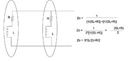
도 10은 도 7의 회로 모델에 대한 최종 테브닌 등가 회로를 예시한 도면.FIG. 10 illustrates a final Thevenin equivalent circuit for the circuit model of FIG. 7. FIG.
도 11은 등가 안테나 회로, 공진 커패시턴스, 및 송수신기를 예시한 도면.11 illustrates an equivalent antenna circuit, resonant capacitance, and transceiver.
도 12 및 도 13은 단일 안테나의 시뮬레이션을 예시한 도면.12 and 13 illustrate the simulation of a single antenna.
도 14 및 도 15는 동일 주파수에서 공진하는 병렬로 접속된 2개의 안테나에 대한 시뮬레이션을 예시한 도면.14 and 15 illustrate simulations of two antennas connected in parallel resonating at the same frequency.
<도면의 주요 부분에 대한 부호의 설명><Explanation of symbols for the main parts of the drawings>
400: 시계 장치400: clockwork
402: 전자 시스템402: electronic system
412: DSP412: DSP
406: 송수신기406: transceiver
본 발명은 일반적으로 모바일 전자 장치에 관한 것이다. 보다 구체적으로는, 본 발명은 모바일 전자 장치용 안테나 시스템에 관한 것이다.The present invention relates generally to mobile electronic devices. More specifically, the present invention relates to an antenna system for a mobile electronic device.
사회가 점차로 유동적이 되어감에 따라, 모바일 전자 장치는 시시각각 변화는 유행과 성장의 물결을 맞이하고 있다. 휴대폰, 무선 PDA, 무선 랩톱 및 다른 모바일 통신 장치는 주류 소비자들에게 강한 인상을 심어 주고 있다. 그러나, 이런 성장을 저해하고 소비자의 만족도를 제한하게 되는 원인은 실제로 넓은 지역을 망라하는, 경제적인, 소형의, 배터리 효율적인 무선 통신 시스템이 부족하다는 데 에 있다. 셀룰러 데이터 송신 전화통신 기반의(Cellular data-transmit telephony-based) 해법들은 전력 효율적인 것과는 거리가 멀고, (상대적으로) 비용과 크기 부담을 지우므로 그들을 사용할 수가 없게 된다.As society becomes increasingly fluid, mobile electronic devices are facing a trend of fashion and growth. Cell phones, wireless PDAs, wireless laptops and other mobile communication devices have made a strong impression on mainstream consumers. However, the impediment to this growth and limiting consumer satisfaction is the lack of economical, compact, battery-efficient wireless communications systems that actually cover large areas. Cellular data-transmit telephony-based solutions are far from power efficient, and (relatively) cost and size burdens make them unusable.
저산만성(Low-distraction) 사용자 인터페이스, 신 운영 체제 플랫폼, 및 새로운 통신 능력을 포함하는 다양한 신 기술들이 개발되고 있다. 스마트 개인 객체들(Smart Personal Objects)은 전용 소프트웨어를 이용하여 보다 스마트한, 보다 개인화되고, 보다 유용하게 된 시계, 펜, 열쇠고리, 가죽지갑 등의 일상의 객체들(objects)이다. 이런 일상의 객체들은 이미 상당히 많이 존재하고 있으며, 물론 그것들 모두는 사람들이 가치있다고 발견한 기본적인 기능들을 이미 가지고 있다. 또한, 그것들은 단지 시간만이 아니라 교통 정보, 스케줄 갱신, 뉴스 등 시간 결정적이고(time-critical) 인간에게 유용한 임의 정보를 적시에 디스플레이하도록 확장될 수 있다.Various new technologies are being developed, including low-distraction user interfaces, new operating system platforms, and new communication capabilities. Smart Personal Objects are everyday objects such as watches, pens, key chains, and leather wallets that have become smarter, more personalized and more useful with dedicated software. Many of these everyday objects already exist, and of course all of them already have the basic functions people find valuable. In addition, they can be extended to display timely and arbitrary information useful for humans, such as traffic information, schedule updates, news, as well as time.
정보를 수신하고 이용하는 이런 객체들의 능력은 각 객체의 신호 송수신 기능에 부분적으로 의존하고 있다. 어떤 응용의 경우, 정보를 송신하기 위해 FM 주파수 대역의 소정 부분을 이용하는 것이 바람직하다. 그러나, 잠재적인 문제가 FM 신호들의 효율적인 이용을 방해할 수 있다. 예를 들면, FM 및 높은 주파수의 막대형 안테나의 인덕턴스량은 (페라이트 손실을 제외하더라도) 급격히 증가하는 경향이 있다. 통상적으로, 인덕턴스가 증가하면 커패시턴스는 감소된다. 그러나 인쇄 배선 기판 트레이스(PWB traces)(또는 인쇄 회로 기판 트레이스(PCB traces)) 및 집적 회로(IC) 패키지, 및 수신기 IC는 탱크 회로에서 최소한의 커패시턴스를 달성 하도록 설정된 커패시턴스를 갖는다. IC 입력은 전형적으로 고 임피던스이며, 정합 회로(matching circuit)를 사용하면 더 많은 손실을 포함하게 되는 경향이 있다. 정합 회로는 부유 용량(stray capacitance)도 포함하는 경향이 있다. 또한, 임의 타입의 마이크로-스트립 정합을 이용하는 것도 바람직하지 않는데, 왜냐하면 휴대형 장치의 PWB 크기(demensions)에 비하여 파장(wavelengths)이 너무 길기 때문이다. 그러므로, 모바일 전자 장치의 경우 보다 강인한(robust) 안테나 시스템이 요망된다.The ability of these objects to receive and use information depends in part on the signaling capabilities of each object. For some applications, it is desirable to use some portion of the FM frequency band to transmit information. However, potential problems can hinder the efficient use of FM signals. For example, the amount of inductance of FM and high frequency rod antennas tends to increase rapidly (except for ferrite losses). Typically, the capacitance decreases as the inductance increases. However, printed wiring board traces (or printed circuit board traces) and integrated circuit (IC) packages, and receiver ICs, have capacitances set to achieve minimal capacitance in the tank circuit. IC inputs are typically high impedance and using matching circuits tend to include more losses. Matching circuits also tend to include stray capacitance. It is also undesirable to use any type of micro-strip matching because the wavelengths are too long for the PWB dimensions of the portable device. Therefore, a more robust antenna system is desired for mobile electronic devices.
저전력 휴대형 컴퓨터에서, 본 발명은 소스로부터 정보를 수신하기 위해 병렬로 접속된 적어도 2개의 안테나를 이용한다. 본 발명의 일 실시예에 따르면, 안테나 시스템은 주파수 변조(FM) 신호의 수신율을 개선시키기 위해 적어도 2개의 복수 루프 안테나를 포함한다. 이 안테나 시스템은 서로에 대해 병렬 접속된 2개의 안테나를 안테나 회로에 포함하여, 유도 전압(induced valtage)에 실제적으로 영향을 주지 않으면서 인덕턴스를 감소시킨 등가 회로가 형성된다. 안테나 시스템은 각각의 안테나에 대해 더 높은 인덕턴스 및 방사 저항(radiation resistance)을 허용하면서, 안테나 동조(tuning)를 위해 조절가능한 커패시턴스 값을 허용한다. 본 발명에 의하면 스폿(SPOT) 장치와, 다른 고주파(HF:3-30Mz,파장: 100m-10m), 초단파(VHF:30-300MHz, 파장:10m-1m), 및 극초단파(UHF:300-3000MHz, 파장:1m-10cm) 장치들이 개선된 감도(sensitivity)와 구성의 용이성을 가지게 된다.In low power portable computers, the present invention utilizes at least two antennas connected in parallel to receive information from a source. According to one embodiment of the invention, the antenna system comprises at least two multiple loop antennas to improve the reception of frequency modulated (FM) signals. The antenna system includes two antennas connected in parallel with each other in the antenna circuit, so that an equivalent circuit is formed which reduces inductance without actually affecting the induced valtage. The antenna system allows for adjustable capacitance values for antenna tuning while allowing higher inductance and radiation resistance for each antenna. According to the present invention, a spot device, another high frequency (HF: 3-30 Mz, wavelength: 100 m-10 m), ultra high frequency (VHF: 30-300 MHz, wavelength 10 m-1 m), and ultra high frequency (UHF: 300-3000 MHz Devices with wavelengths of 1m-10cm have improved sensitivity and ease of configuration.
본 발명에 대한 보다 완벽한 인식과 개선점은 이후에 간단히 요약되며 첨부 된 도면과 그 다음의 본 발명의 예시적인 실시예에 대한 상세한 설명 및 청구항을 참조하여 얻어질 수 있다.A more complete recognition and improvement of the present invention will be briefly summarized below and obtained by reference to the accompanying drawings and the following detailed description and claims of exemplary embodiments of the present invention.
본 발명은 PDA, 휴대폰, 페이저, 스마트폰, 카메라폰 등의 무선 클라이언트 장치의 관점에서 기술된다. 바람직한 실시예에서, 클라이언트 장치는 통신 신호를 수신하도록 특별히 구성된 시계형 장치이다.The present invention is described in terms of wireless client devices such as PDAs, cell phones, pagers, smartphones, camera phones, and the like. In a preferred embodiment, the client device is a watch-type device specifically configured to receive a communication signal.
본 발명은 전자 장치용 안테나 시스템을 제공한다. 보다 구체적으로는, 본 발명은 모바일 전자 장치에서의 고주파, 초단파, 극초단파 신호의 수신율을 개선시키는 모바일 전자 장치용 안테나 시스템을 제공한다. 바람직한 실시예에 따르면, 안테나 시스템은 서로 병렬로 접속된 제1 및 제2 안테나를 안테나 회로에 포함한다. 병렬 안테나 구조에 의해 유도 전압에 실제적으로 영향을 주지 않으면서 인덕턴스를 감소시킨 등가 회로가 형성된다. 안테나 시스템은 각각의 안테나에 대해 더 높은 인덕턴스 및 방사 저항을 허용하면서, 안테나 동조를 위해 조절가능한 커패시턴스 값을 허용하는 경향이 있다.The present invention provides an antenna system for an electronic device. More specifically, the present invention provides an antenna system for a mobile electronic device that improves reception rates of high frequency, microwave and microwave signals in a mobile electronic device. According to a preferred embodiment, the antenna system comprises in the antenna circuit first and second antennas connected in parallel with each other. The parallel antenna structure forms an equivalent circuit that reduces inductance without actually affecting the induced voltage. Antenna systems tend to allow adjustable capacitance values for antenna tuning, while allowing higher inductance and radiation resistance for each antenna.
이후에 기술된 바와 같이, 전자 장치는 통신 신호들을 수신 및/또는 송신하도록 특별히 구성된 스마트 시계형 장치일 수 있다. 소정의 실시예가 시계 기반의 시스템의 관점에서 기술되었지만, 본 응용의 교시는 다른 휴대형 컴퓨터, PDA, 휴대폰, 알람 시계(alarm clock), 열쇠고리, 냉장고에 붙이는 자석(refrigerator magnet) 등에도 동등하게 적용될 수 있다는 것은 분명할 것이다. 시계를 이용한 것은 예시적인 목적에서 이후의 논의를 간단히 하기 위함이고, 이것은 "모바일 장 치" 및/또는 "클라이언트 장치"와 상호 교환해서 사용될 수 있다.As described later, the electronic device may be a smart watch-type device specifically configured to receive and / or transmit communication signals. Although certain embodiments have been described in terms of clock-based systems, the teachings of this application are equally applicable to other portable computers, PDAs, mobile phones, alarm clocks, key rings, refrigerator magnets, and the like. It will be clear. The use of a clock is intended to simplify the following discussion for illustrative purposes, which may be used interchangeably with "mobile device" and / or "client device".
"컴퓨터 판독가능 매체"는 클라이언트/서버 장치에 의해 액세스될 수 있는 임의 이용가능한 매체일 수 있다. 예로서, 컴퓨터 판독가능 매체는 컴퓨터 저장 매체 및 통신 매체를 포함할 수 있다. 컴퓨터 저장 매체는 컴퓨터 판독가능 명령어, 데이터 구조, 프로그램 모듈 또는 기타 데이터 등의 정보를 저장하기 위한 임의 방법 또는 기술이 구현된 휘발성 비휘발성, 분리형 비분리형 매체를 포함하나 이에만 한정되지 않는다. 컴퓨터 저장 매체는 클라이언트/서버 장치에 의해 액세스될 수 있는 원하는 정보를 저장하는데 사용될 수 있는 RAM, ROM, EEPROM, 플래시 메모리, 또는 기타 메모리 기술, CD-ROM, 디지털 다목적 디스크(DVD) 또는 기타 광 저장장치, 자기 카세트, 자기 테이프, 자기 디스크 저장 장치 또는 임의 기타 매체를 포함하나 이에만 한정되지 않는다.A "computer readable medium" can be any available medium that can be accessed by a client / server device. By way of example, computer readable media may comprise computer storage media and communication media. Computer storage media includes, but is not limited to, volatile nonvolatile, removable non-removable media implemented with any method or technology for storing information such as computer readable instructions, data structures, program modules or other data. Computer storage media may include RAM, ROM, EEPROM, flash memory, or other memory technology, CD-ROM, digital versatile disk (DVD), or other optical storage that may be used to store desired information accessible by client / server devices. Including but not limited to devices, magnetic cassettes, magnetic tapes, magnetic disk storage devices or any other media.
통신 매체는 전형적으로 컴퓨터 판독가능 명령어, 데이터 구조, 프로그램 모듈, 또는 기타 데이터를 반송파 또는 기타 전송 메커니즘 등을 변조된 데이터 신호에 구현한 것이며, 임의 정보 전송 매체를 포함한다. "변조된 데이터 신호"란 용어는 어떤 신호의 하나 이상의 특성을 그 신호에 실린 정보를 부호화하는 방식으로 설정 또는 변경시킨 신호를 의미한다. 예로서, 통신 매체는 유선 네트워크 또는 유선에 의한 직접 접속 등의 유선 매체와, 음파, RF, 적외선 등의 무선 매체와, 기타 무선 매체를 포함하나, 이에만 한정되지 않는다. 상기의 임의의 것들을 조합한 것도 컴퓨터 판독가능 매체 범위 내에 포함된다.A communication medium is typically an implementation of computer readable instructions, data structures, program modules, or other data in a modulated data signal that includes a carrier or other transmission mechanism, and includes any information transmission medium. The term " modulated data signal " means a signal that has one or more of its characteristics set or changed in such a manner as to encode information carried on that signal. By way of example, communication media includes, but is not limited to, wired media such as a wired network or direct connection by wire, wireless media such as sound waves, RF, infrared light, and other wireless media. Combinations of any of the above are also included within the scope of computer readable media.
"콘텐츠"란 용어는 전자 장치에 저장될 수 있는 임의 정보가 될 수 있다. 예로서, 콘텐츠는 그래픽 정보, 텍스트 정보, 및 그래픽과 텍스트 정보의 임의 조합한 것을 포함할 수 있으나 이에만 한정되지 않는다. 콘텐츠는 디스플레이 가능한 정보 또는 청각 정보일 수 있다. 청각 정보는 단일 사운드 또는 사운드 스트림을 포함할 수 있다.The term "content" may be any information that can be stored in an electronic device. By way of example, the content may include, but is not limited to, graphical information, text information, and any combination of graphics and text information. The content may be displayable information or auditory information. Auditory information may include a single sound or a sound stream.
본 발명의 전체적인 동작 환경은 도 1 및 도 2를 참조하여 이후에 논의될 것이다.The overall operating environment of the present invention will be discussed later with reference to FIGS. 1 and 2.
동작 환경Operating environment
도 1은 본 발명의 예시적인 동작 환경(100)을 예시한다. 이 도면에서 예시된 바와 같이, FM 송수신기 및 방송은 통신 채널(110)을 통해 다양한 전자 장치들로 송신된다. FM 수신기 또는 송수신기를 갖는 예시적인 전자 장치는 데스크탑 컴퓨터, 시계, 휴대형 컴퓨터, 무선 휴대폰(cell phone), 및/또는 PDA를 포함할 수 있다. 전자 장치는 FM 방송으로부터 정보를 수신하도록 구성된다. FM 방송은 원하는 바대로 표준 FM 송신, 부반송파(sub-carrier) FM 송신, 또는 임의 기타 유형의 FM 송신을 포함하나 이에만 한정되지 않고 여러 유형이 될 수 있다.1 illustrates an
상호작용 모델에 따라 동작하도록 구성된 전자 시스템을 포함할 수 있는 예시적인 전자 장치가 도 1에 예시되어 있다. 전자 시스템은 상기 기술한 FM 송신 시스템 등의 무선 인터페이스를 이용할 수 있다. 각각의 전자 시스템은 통신 채널을 통해 메시지/정보를 수신한다.An example electronic device that may include an electronic system configured to operate according to an interaction model is illustrated in FIG. 1. The electronic system can use a wireless interface such as the FM transmission system described above. Each electronic system receives messages / information via a communication channel.
도시되고 기술된 동작 환경은 적합한 동작 환경에 대한 예시일 뿐이며, 본 발명의 기능 또는 사용 범위에 대하여 제한을 가하려는 의도가 아니다. 본 발명을 이용하기에 적합할 수 있는 기타 공지된 컴퓨팅 시스템, 환경, 및/또는 구성은 상기 시스템들 또는 장치들 중 임의 것을 포함하는 개인용 컴퓨터, 서버 컴퓨터, 휴대형 또는 랩톱 장치, 마이크로프로세서 시스템, 마이크로프로세서 기반의 시스템, 프로그램가능한 소비자 가전기기, 네트워크 PC, 미니컴퓨터, 메인프레임 컴퓨터, 및 분산 컴퓨터 환경 등을 포함하나 이에만 한정되지 않는다.The operating environment shown and described is merely an example of a suitable operating environment and is not intended to limit the functionality or scope of use of the invention. Other known computing systems, environments, and / or configurations that may be suitable for using the present invention include personal computers, server computers, portable or laptop devices, microprocessor systems, microcomputers, including any of the above systems or devices. Processor-based systems, programmable consumer electronics, network PCs, minicomputers, mainframe computers, and distributed computer environments.
예시적인 전자 시스템Example Electronic System
도 2는 예시적인 전자 장치(200)의 기능적 컴포넌트들을 예시한 개략도이다. 전자 장치(200)는 프로세서(260), 메모리(262), 디스플레이(228), 및 사용자 인터페이스(232)를 갖는다. 메모리(262)는 일반적으로 휘발성 메모리(예컨대, RAM), 및 비휘발성 메모리(예컨대, ROM, 플래시 메모리 등) 모두를 포함한다. 전자 장치(200)는 마이크로소프트사의 Windows CE 운영 체제 또는 기타 운영 체제와 같이 메모리(262)에 존재하며 프로세서(260) 상에서 실행되는 운영 체제(264)를 포함한다. 사용자 인터페이스(232)는 일련의 누름 버튼, 스크롤 휠(scroll wheel), 숫자 다이얼링 패드(전형적 전화기 등), 또는 기타 유형의 사용자 인터페이스 수단일 수 있다. 디스플레이(228)는 전자 장치에 통상적으로 사용되는 액정 표시 장치(liquid crystal display), 다수의 비트 표시기, 또는 풀 컬러 디스플레이, 또는 임의 다른 유형의 디스플레이일 수 있다. 일 실시예에서, 디스플레이(228)는 입력 장치로서 동작하는 터치-형(touch-sensitive)일 수 있다.2 is a schematic diagram illustrating functional components of an example
하나 이상의 애플리케이션 프로그램들(266)은 메모리(262) 내로 로드되어 운영 체제(264) 상에서 실행된다. 애플리케이션 프로그램들의 예로서 폰 다이얼러 프로그램(Phone dialer program), 이메일 프로그램, 스케줄링/달력 프로그램, PIM(개인 정보 관리) 프로그램, 및 인터넷 브라우저 프로그램 등을 포함한다. 전자 장치(200)는 또한 메모리(262) 내에 위치하는 비휘발성 저장 장치(268)를 포함한다. 비휘발성 저장 장치(268)는 전자 장치(200)의 전원 공급이 중단될 경우 손실되어서는 안 되는 영속적인 정보를 저장하는데 사용될 수 있다. 애플리케이션들(266)은 이메일 애플리케이션에 의해 사용되는 이메일 또는 기타 메시지와, PIM에 의해 사용되는 접속 정보, 스케줄링 프로그램에 의해 사용되는 약속 정보, 워드 프로세싱 애플리케이션에 의해 사용되는 문서 등의 정보를 저장 장치(258)에 저장하고 이를 사용할 수 있다.One or
전자 장치(200)는 하나 이상의 배터리로 구현될 수 있는 전원(270)을 갖는다. 또한, 전원(270)은 배터리를 충전하거나 재충전하는 AC 어댑터 또는 전력 공급된 도킹 크레이들(docking cradle) 등의 외부 전원도 포함한다.The
전자 장치(200)는 두 가지 유형의 외부 통지 메커니즘, 즉 LED(240) 및 오디오 인터페이스(274)를 갖는 것으로 도시되어 있다. 이런 장치들은 전원(270)에 직접 결합될 수 있어서, 배터리 전력을 보존하기 위해 프로세서(260)와 기타 컴포넌트들이 셧 다운(shut down)될지라도, 활성화될 때 통지 메커니즘에 의해 지시받은 기간 동안 유지된다. LED(240)는 사용자가 장치가 파워-온 상태임을 지시하는 동작을 취할 때까지 무기한 유지되도록 프로그래밍될 수 있다. 오디오 인터페이스(274)는 사용자로부터 청각적인(audible) 신호를 수신하고, 사용자에게 청각적인 신호를 제공하는데 사용된다. 예를 들면, 오디오 인터페이스(274)는 들을 수 있는 출력을 제공하기 위해 스피커에 결합되고, 음성 인식을 이용하는 사용자 인터페이스로서 전화기 대화를 용이하게 하는 청각적인 입력을 수신하기 위한 마이크로폰에 결합될 수 있다. 다른 예에서, 음향 진동 장치(도시 생략)는 새로 도달한 메시지에 대해 사용자에게 알려주는 것 등의 피드백을 사용자에게 제공하는데 사용될 수 있다. 전자 장치(200)는 각각의 경보 메커니즘(예컨대, 오디오, 음향 진동뿐 아니라 비주얼 큐)을 개별적으로 제어할 수 있다.The
또한, 전자 장치(200)는 무선 주파수(Radio frequency) 통신을 수신하고/송신하는 기능을 수행하는 무선 인터페이스 계층을 포함한다. 무선 인터페이스 계층(272)은 무선 반송파 또는 서비스 제공자를 통하여 전자 장치(200)와 외부 세계 간의 무선 접속을 용이하게 한다. 무선 인터페이스 계층(272)으로의 송수신은 운영 체제(264)의 제어를 받으며 시행된다. 즉, 무선 인터페이스 계층(272)에 의해 수신된 통신은 운영 체제(264)를 통하여 애플리케이션 프로그램들(266)로 및 그 반대로 보급될 수 있다.In addition, the
본 발명의 일 실시예에서, 전자 장치(200)는 무선 인터페이스를 포함하는 시계 장치 등의 모바일 전자 장치이다. 시계 장치의 경우 예시적인 사용자 인터페이스는 이후에 기술되어 있듯이, 도 3a에 도시되어 있다. 비록 이후에 기술된 사용자 인터페이스 구성은 다수의 선택 버튼(예컨대, 4개의 선택 버튼)을 포함하고 있으나, 다수의 선택 버튼의 기능들이 단일 선택자(예컨대, 버튼, 로켓 스위치, 휠 등)에 결합될 수 있다.In one embodiment of the invention, the
사용자 인터페이스(UI)User interface (UI)
도 3은 순간식별가능한(glanceable) 정보 기술을 이용하도록 구성된 사용자 인터페이스를 포함하는 예시적인 시계 장치(300)를 예시한다. 시계 장치(300)는 전자 시스템(예컨대, 도 2 참조)을 갖는 베젤(Bezel:310)을 포함한다. 전자 시스템은 도 2에 관하여 이전에 기술된 하드웨어와 일치하는 방식으로 기능들을 수행한다. 베젤(310)은 액정 표시 장치, 다수의 비트 표시기, 또는 풀 컬러 디스플레이 등의 디스플레이(320)를 갖는다. 일 실시예에서, 시계 밴드는 디스플레이(320) 상에 전자식으로 생성된다. 다른 대안적 실시예에서, 베젤은 디스플레이(320)에 손실을 입히는 간섭을 발생시키지 않는 아날로그형 시계 밴드를 포함한다. 시계 장치(300)는 사용자 인터페이스(UI)로서 동작하도록 구성된 일련의 버튼(330a 부터 330e)들을 포함한다.3 illustrates an
각각의 버튼들은 사용자 인터페이스의 선택자(selector)로서 동작한다. 모든 버튼은 디폴트 기능, 및/또는 컨텍스트 결정된 기능을 가진다. 현재 선택된 채널은 각각의 선택자에 대한 컨텍스트를 결정한다. 대안으로서, 현재 활성화된 디스플레이는 각각의 선택자에 대한 컨텍스트를 결정한다. 예를 들면, 디스플레이 스크린(예컨대, 도움말 스크린)은 메인 스크린 상에서 겹쳐 놓여질(superimposed) 수 있어서, 그 디스플레이 스크린이 활성 컨텍스트가 된다. 전자 장치(300)는 각각의 선택자에 연관된 기능이 선택된 채널 또는 디스플레이 스크린에 기반하여 변경될 수 있다는 점에서 컨텍스트에 감응한다(context sensitive)고 한다.Each button acts as a selector of the user interface. Every button has a default function, and / or a context determined function. The currently selected channel determines the context for each selector. As an alternative, the currently active display determines the context for each selector. For example, a display screen (eg, a help screen) can be superimposed on the main screen so that the display screen becomes the active context. The
모바일 전자 장치용 안테나 시스템Antenna system for mobile electronics
본 발명은 전자 장치용 안테나 시스템을 제공한다. 보다 구체적으로는, 본 발명은 모바일 전자 장치에서의 고주파, 초단파, 극초단파 신호들의 수신율을 개선시키기 위한, 시계 등의 모바일 전자 장치용 안테나 시스템을 제공한다. 바람직한 실시예에 따르면, 안테나 시스템은 서로에 대해 병렬 연결된 제1 및 제2 안테나를 안테나 회로에 포함한다. 병렬 안테나 구조에 의해 유도 전압에 실제적으로 영향을 주지 않으면서 인덕턴스를 감소시킨 등가 회로가 형성된다. 안테나 시스템은 각각의 안테나에 대해 더 높은 인덕턴스 및 방사 저항을 허용하면서, 안테나 동조를 위해 조절가능한 커패시턴스 값을 허용하는 경향이 있다. 상술된 실시예에서, 전자 장치는 통신 신호를 수신 및/또는 송신하도록 특별히 구성된 스마트 시계형 장치일 수 있다.The present invention provides an antenna system for an electronic device. More specifically, the present invention provides an antenna system for a mobile electronic device such as a watch for improving reception rates of high frequency, microwave and microwave signals in a mobile electronic device. According to a preferred embodiment, the antenna system comprises in the antenna circuit first and second antennas connected in parallel with each other. The parallel antenna structure forms an equivalent circuit that reduces inductance without actually affecting the induced voltage. Antenna systems tend to allow adjustable capacitance values for antenna tuning, while allowing higher inductance and radiation resistance for each antenna. In the above-described embodiment, the electronic device may be a smart watch-type device specially configured to receive and / or transmit a communication signal.
이후의 논의는 시계 장치 및 유사 전자 시스템을 위한 안테나 시스템에 관한 것이다. 그러나, 본 발명이 시계 장치에만 한정되는 것이 아님을 인식할 것이며, 당업자는 다른 모바일 및 휴대형 전자 장치의 경우에도 본 발명의 이점을 실현할 수 있다.The following discussion relates to antenna systems for watch devices and similar electronic systems. However, it will be appreciated that the present invention is not limited to watch devices, and those skilled in the art can realize the advantages of the present invention in the case of other mobile and portable electronic devices.
예시적인 시계 장치(400)는 도 4에 도시되어 있다. 시계 장치(400)는 본 발명에 따라 동작하도록 구성된 전자 시스템(402)을 포함한다. 전자 시스템(402)은 도 4에 도시된 바와 같은 베젤 내에 혹은 시계 장치의 어떤 다른 부분에 포함될 수 있다. 또한, 시계 장치(400)는 시계를 사용자 손목에 부착시키는 시계밴드(404)를 포함할 수 있다.An
전자 시스템(402)은 장치의 수신기 및/또는 송수신기로서 동작하는 기능을 포함한 컴퓨터 기반의 시스템이다. 도면에 도시된 바와 같이, 전자 시스템은 송수신기(406), 마이크로컴퓨터 유닛 또는 마이크로프로세서(408), 및 아날로그 라디오(410:RADIO)를 포함한다. 이하에 자세히 기술된 바와 같이, 안테나는 정보 신호들을 송출 및/또는 수신하기 위해 송수신기(406)에 접속되어 있다. 마이크로프로세서(408)와 라디오(RADIO) 컴포넌트 간의 트랜잭션(transactions)은 마이크로프로세서-디지털 송수신기 인터페이스를 통해 조정된다. 시계 장치(400)의 컴포넌트들은 시계 크기의 인클로저(enclosure) 내에 수용되고 동작을 위해 배터리 전력에 의존한다.
송수신기(406)는 일반적으로 송수신기를 위한 제어, 스케줄링, 및 사후 프로세싱 태스크들을 수행하는 디지털 신호 처리기(412:DSP)와, 디지털 라디오(RADIO), 시스템 타이밍, 및 실시간 이벤트 디스패칭(dispatching)을 포함하는 실시간 장치(414:RTD)를 포함한다. DSP(412)는 마이크로프로세서(408)에 결합되고, 송수신기 태스크들은 마이크로프로세서(408)에 의해 명령을 받는다.The
DSP의 태스크 중 하나는 부반송파 위상 회복, 보우 회복(baud recovery) 및/또는 추적(tracking), 페이딩 효과에 대한 보상, 복조, 디인터리빙(de-interleaving), 및 채널 상태 평가 및/또는 에러 정정 등의 목적을 위해 수신된 데이터를 처리할 수 있다. 패킷에 대한 사후 프로세싱은 전체 패킷이 수신되면 발생할 수 있거나 그 이후에 발생할 수 있다. DSP는 전송된 데이터 패킷을 분석하여 RTD(414)의 로컬 클럭에 관해서 방송국의 신호 타이밍을 결정한다. 로컬 클럭이 신호 샘플링시 무결성(signal sampling integrity)을 유지하기 위해 송신기의 클럭 신호에 동기화된다. 수신기는 주기적으로 송신기와의 심볼 동기화(symbol synchronization)에 동참하여 수신된 신호의 오역(misreading)을 최소화한다.One of the tasks of the DSP is subcarrier phase recovery, baud recovery and / or tracking, compensation for fading effects, demodulation, de-interleaving, and channel condition evaluation and / or error correction. The received data can be processed for the purpose of Post-processing for the packet may occur when the entire packet is received or may occur thereafter. The DSP analyzes the transmitted data packet to determine the signal timing of the broadcast station with respect to the local clock of the
RTD(414)의 디지털 부(digital section)는 마이크로프로세서(408)와 DSP(412)에 시스템 클럭을 제공하는 수정 발진기(crystal oscillator) 등의 시스템 타임-기반 발진기를 포함할 수 있다. 또한, 타임-기반은 보우 및 샘플 타이밍을 송신과 수신 동작에, 시작/종료 제어를 무선 동작에 제공하고, 마이크로프로세서(408)와 DSP(412)에 대한 클럭 미결정 주기(the periods of clock suspension)를 제어한다. RTD(414)는 무선 동작들도 수행하고, 부가 동작들도 수행할 수 있다. 라디오(410:RADIO)는 패킷을 형성하는 데이터 세그먼트들을 수신하도록 구성된다.The digital section of the
이제 도 5a부터 도 5c를 참조하면, 본 발명의 바람직한 실시예에 따르는 안테나 시스템(500)이 도 4의 시계 장치(400)에 관련하여 기술된 송수신기 등의 송수신기(502:RF IC)에 전기적으로 접속된 것으로 도시된다. 이런 실시예에 따르는 송수신기(502)는 아날로그 신호 처리 능력, 발진기, 위상 고정 루프(PLL), ADC를 포함하고, 안테나 동조 제어를 제공한다. 도 5a에 도시된 바와 같이, 송수신기는 디지털 IC(503)와 통신한다. 디지털 IC(503)는 프로세서, 메모리, 디지털 승산기(multiplier), 및 필터를 포함한다. 디지털 IC(503)는 LCD 등의 디스플레이(505)와 통신한다. 전원(507)은 전원 회로(509)를 통해 전력을 장치에 제공한다. RFIC(512)는 공진하는 탱크 회로로서 안테나를 동조시키는 동작을 할 수 있고, 증폭(amplification), 혼합(mixing), 및 아날로그 대 디지털 변환을 제공한다. 디지털 IC(503)는 디지털 신호 처리, 시스템 레벨 타이밍 및 제어, 사용자 I/O를 제공하도록 동작할 수 있다.Referring now to FIGS. 5A-5C, an
안테나 시스템(500)은 보오사이트(boresight), 하나 이상의 널(null), 및 약 100MHz에서 -25dBi 정도의 안테나 이득을 포함하는 관련 안테나 패턴을 갖는다. 이런 이득은 안테나 방향성과 효율을 포함한다. 특정 안테나 값은 시계 장치의 동작 주파수에 따라 변경된다는 점을 인식해야 한다. 시계 장치는 각 경우에 대해 자동 동조되도록 동작할 수 있고, 안테나 널이 정보 소스를 향하고 있을 때 데이터를 프로세싱하는 순방향 에러 계산 알고리즘을 포함한다. 또한, 본 명세서에 기술된 안테나 시스템은 애플리케이션을 단지 송신하고 수신하는 것에도 적용가능하다는 점을 인식해야 한다.
도 5a를 계속 참조하면, 안테나 시스템(500)은 서로 병렬로 전기적으로 접속된 제1 안테나(504)와 제2 안테나(506)를 포함한다. 바람직한 실시예에 따르면, 각 안테나(예컨대, 구리 나선형 호일(copper spiral foil)을 사용함)의 한쪽 종단(504A 및 506A)은 송수신기 회로소자의 구리 트레이스의 한쪽 종단(트레이스 상에서 납땜으로 접속된 양쪽 종단을 "단자"로 기술할 수 있음)에 부착되어 있다. 이후에 기술된 대로, 도 5b를 참조하면 본 발명의 일 실시예에 따르는 구리 트레이스의 다른 쪽 종단은 칩 핀(522, 524, 및 526)(RX+, TX+, CAP1+)에 부착되어 있다. 유사한 방식으로, 각 안테나의 다른 쪽 종단(504B 및 506B)은 송수신기 회로소자의 다른 쪽 구리 트레이스에 부착되어 있다. 구리 트레이스의 다른 쪽 종단은 칩 핀(516, 518, 및 520)(RX-,TX-, CAP1-)에 부착되어 있다.With continued reference to FIG. 5A, the
일 실시예에서, 병렬 안테나 조합의 한 단자는 칩 핀(516, 518, 및 520)(RX-,TX-, CAP1-)에 접속되어 있고, 병렬 안테나 조합의 다른 쪽 단자는 칩 핀(522, 524, 및 526)(RX+, TX+, CAP1+)에 부착되어 있다. 대안적 실시예에서, CAP2 뱅크는 병렬 안테나 조합의 한 단자를 칩 핀(516, 518, 및 528)(RX-,TX-, CAP2-)에 접속시키는 데 사용될 수 있고, 병렬 안테나 조합의 다른 쪽 단자는 칩 핀(522, 524, 및 530)(RX+, TX+, CAP2+)에 부착되어 있다. 다른 대안적 실시예에서, CAP1 뱅크와 CAP2 뱅크 모두는 병렬 안테나 조합의 한 단자를 칩 핀(516, 518, 520, 및 528)(RX-, TX-, CAP1-, CAP2-)에 접속시키는 데 사용될 수 있으며, 병렬 안테나 조합의 다른 쪽 단자는 칩 핀(522, 524, 526, 및 530)(RX+, TX+, CAP1+, CAP2+)에 부착되어 있다.In one embodiment, one terminal of the parallel antenna combination is connected to chip
송수신기(502:RF IC)는 구체적인 뱅크 또는 뱅크들을 갖고 병렬로 접속된 인덕턱스량에 기반하여 약 5pf부터 약 35pf까지 커패시턴스를 조절하도록 동작가능하다. 예를 들면, CAP1 뱅크가 접속될 경우, 인덕턴스량은 약 94nH부터 약 218nH일 수 있다. CAP2 뱅크가 접속될 경우, 인덕턴스량은 약 94nH부터 약 218nH일 수 있다. CAP1과 CAP2가 모두 접속될 경우, 인덕턴스량은 약 47nH부터 약 109nH일 수 있다. 그러므로, CAP1 뱅크, CAP2 뱅크, 또는 양자가 구체적인 모바일 전자 장치와 그 관련된 응용에 기반하여 안테나 시스템의 일부로서 구현될 수 있다.The transceiver 502 (RF IC) is operable to adjust capacitance from about 5pf to about 35pf based on the amount of inductance connected in parallel with a specific bank or banks. For example, when the CAP1 bank is connected, the inductance amount may be about 94nH to about 218nH. When the CAP2 bank is connected, the inductance amount can be from about 94nH to about 218nH. When both CAP1 and CAP2 are connected, the inductance amount may be about 47nH to about 109nH. Therefore, the CAP1 bank, the CAP2 bank, or both may be implemented as part of the antenna system based on the specific mobile electronic device and its associated application.
바람직한 실시예에 따르면, 제1 안테나(504)는 약 40mm 길이를 가지며, 약 8mm의 지름을 가진다. 이런 실시예에 따르면, 도 5c에 도시된 바와 같은 제1 안테나(504)는 구리 테이프(510)로 래핑되어(wraped) 막대에 복수의 루프를 갖게 된 페라이트 막대(508)를 포함하며, 이것은 평면 나선형 권선(winding) 구조를 정의한다. 또한, 제2 안테나(506)도 약 40mm 길이를 가지며, 약 8mm 지름을 포함한다. 또한, 제2 안테나(506)도 구리 테이프(514)로 래핑된 페라이트 막대(512)를 포함하는 것이 바람직하다. 안테나의 일부로서 페라이트 막대를 사용하면 각 안테나의 효과적인 방사 저항 및 방사 효율을 효과적으로 증가시킬 수 있다. 이런 실시예에서, 각 안테나는 구리 테이프로 래핑된 페라이트 막대를 포함하고, 각 안테나의 구리 테이프는 3회 권선을 갖는다. 또한, 이런 실시예에 따르면, 각각의 권선은 개별 페라이트 막대에 관하여 인접한 권선으로부터 약 3mm 이격되어 있으며, 그 테이프는 개별 페라이트 막대에 관하여 동일한 방향(도 11에 도시된 바와 같이 각 안테나의 경우 반시계 방향)으로 감겨져 있다. 그러나, 당업자는 구리 테이프가 구체적인 응용과 원하는 결과에 따라 그 보다 적거나 많은 권선들(turns)을 포함할 수 있음을 인식해야 한다.According to a preferred embodiment, the
본 발명에 따르면 안테나 시스템(500)은 각각의 안테나(504 및 506)에 대해 더 높은 인덕턴스 및 방사 저항을 허용하면서, 안테나 동조를 위해 조절가능한 커패시턴스 값을 허용하는 경향이 있다. 이후에 기술한 바와 같이, 안테나 시스템(500)에 의해 유도 전압에 실제적으로 영향을 주지 않으면서 인덕턴스를 감소시킨 등가 회로가 형성된다.According to the present invention,
안테나 시스템의 전파 수신 능력(radio reception capability)은 안테나 시스템(500)을 시스템(500)에 병렬로 놓인 커패시턴스와 공진시킴으로써 증진될 수 있다. 커패시턴스는 안테나의 리액티브(인덕턴스) 성분을 공진시키거나 제거하여서, 수신 신호의 전압이 인덕터에 걸쳐 나타나지 않게 됨으로써 전체적으로 송수신기에서는 이용가능하게 된다. 바람직하게는, 송수신기(502)는 상술된 바와 같이 하나 이상의 커패시턴스 뱅크(도 5b의 커패시턴스 뱅크 CAP1과 CAP2를 참조)를 포함한다. 본 발명의 바람직한 실시예에 따르면, 커패시턴스 뱅크(CAP1 및/또는 CAP2)는 제1 안테나(504) 및 제2 안테나(506)에 병렬로 각기 접속된다. 송수신기(502)는 제1 안테나 및 제2 안테나의 인덕턴스에 기반하여 커패시턴스를 자동으로 조절하도록 동작하고, 즉 제1 안테나 및 제2 안테나와 CAP1 및/또는 CAP2가 발진기를 형성하고, 송수신기(502)는 2진 스테핑 패턴(binary stepping pattern)을 이용하여 정확한 주파수를 발견할 때까지 커패시턴스량을 조절한다.The radio reception capability of the antenna system may be enhanced by resonating the
안테나 시스템(500)의 안테나(504 및 506)는 각각이 페라이트 등의 높은 투자율(permeability) 코어를 구리 테이프 권선 내부에 포함시킨 루프 안테나로서 기술될 수 있다. 그러나, 다른 실시예에 따르면, 각 안테나는 내부 막대 또는 코어 없이 복수의 권선 또는 권선들을 갖는 권선형 도체(wound conductor)를 포함할 수 있다. 전기적으로 소형 루프 안테나(루프의 지름 << 파장)의 경우, 개방 회로 안테나의 단자 양단에 유도된 전압은 노이즈 전압에 비하여 그 크기가 작다. 일부 응용에서, 탱크 회로는 유도 전압의 크기를 증가시키는데 사용될 수 있다. 탱크 회로는 인덕터, 커패시터, 및 선택적으로 저항을 포함하는 병렬 공진 회로이다.
또한, 전압 또는 역기전력(EMF,electro-motive force)(V 또는 EMF = N*(dPHI/dt), 여기서 PHI는 자속(flux)의 양이고 N은 권선수임)에서의 증가는 다수의 권선을 갖는 루프를 이용함으로써 얻어질 수 있다. 그러나, 안테나 시스템을 설계할 때, 도체 손실, 임의 절연체의 유전 손실, 인접 도체의 근접 손실로 인한 손실 vs. 권선수의 절충(trade-off)을 고려해야 한다. 주어진 자기장("H"필드)에 대해 자속 밀도를 증가시키는 다른 방법은 루프 안테나 내부에 더 높은 투자율(μr)을 가진 물질을 삽입하는 것이다. FM 주파수(약 85 부터 108MHz) 및 상위 FM 주파수에서는, 임의의 높은 μr의 물질 손실도 고려해야만 한다.In addition, an increase in voltage or electro-motive force (EMF) (V or EMF = N * (dPHI / dt), where PHI is the amount of flux and N is the number of turns) has multiple windings. Can be obtained by using a loop. However, when designing an antenna system, losses vs. losses due to conductor loss, dielectric loss of any insulator, and proximity loss of adjacent conductors. Consideration should be given to the trade-off of the number of turns. Another way to increase the magnetic flux density for a given magnetic field (“H” field) is to insert a material with a higher permeability μ r inside the loop antenna. At FM frequencies (about 85 to 108 MHz) and higher FM frequencies, any high μ r material loss must also be taken into account.
상술된 바와 같이, 페라이트 막대는 본 발명의 바람직한 실시예에 따르는 안테나 시스템(500)의 각 안테나(504 및 506)의 안테나 코어로서 사용된다. 그러나, 다른 높은 투자율 물질도 이용될 수 있으며, 본 발명은 본 명세서에 기술된 예시와 실시예에 의해서 한정되는 것은 아니다. 또한, 페라이트 또는 다른 높은 투자율 물질 막대를 안테나 코어로서 이용할 경우, 막대 양단을 도체 권선의 가장 자리 쪽으로 확장시킴으로써 자속 밀도가 증강될 수 있다. 더 많은 권선으로 인한 "외부(extra)" 손실은 막대 양단을 도체 권선의 가장 자리 쪽으로 확장시킴으로써 실제적으로 제거될 수 있다.As described above, the ferrite rod is used as the antenna core of each
본 발명에 따라서 상술된 바와 같이, 공진 커패시턴스와 병렬로 하나 이상의 루프 안테나를 접속시킴으로써 등가 회로에서 유도 전압을 실제적으로 동일하게 유지하는 동시에 등가 회로의 인덕턴스를 감소시키는 것이 가능하다. 이것은 예컨대, 장치들의 크기 제약("형태 요소(form factor)")이 주어진 스마트 시계 등의 모바일 전자 장치들의 경우에 특히 바람직하다. 또한, 등가 회로의 손실 저항도 감소된다.As described above in accordance with the present invention, it is possible to connect one or more loop antennas in parallel with the resonant capacitance to reduce the inductance of the equivalent circuit while keeping the induced voltage substantially the same in the equivalent circuit. This is particularly desirable in the case of mobile electronic devices, such as smart watches, for example given the size constraints ("form factor") of the devices. In addition, the loss resistance of the equivalent circuit is also reduced.
단일 루프 안테나의 회로 모델이 도 6에 도시되어 있다. 심볼 R은 도체와 절연체의 손실인 방사 저항을 나타낸다. V는 자기장(V = N*(dPHI/dt))에 의해 유 도된 전압을 나타낸다. 2개의 루프 안테나가 병렬로 접속된 회로 모델은 도 7에 도시되어 있다. 루프 안테나는 전기적으로 작기 때문에, V1과 V2는 (실제적으로 동일한 방향으로 감긴 동일한 루프 안테나의 경우) 위상과 크기에 있어서 등가를 갖는다고 가정된다. 또한, R과 인덕턴스(L)는 실제적으로 동일한 루프 안테나에 대한 이런 예시에 있는 각각의 루프 안테나의 경우에 동일하다. The circuit model of the single loop antenna is shown in FIG. The symbol R represents radiation resistance, which is the loss of conductors and insulators. V represents the voltage induced by the magnetic field (V = N * (dPHI / dt)). A circuit model in which two loop antennas are connected in parallel is shown in FIG. Since the loop antenna is electrically small, it is assumed that V1 and V2 are equivalent in phase and magnitude (in the case of the same loop antenna actually wound in the same direction). Also, R and inductance L are the same for each loop antenna in this example for a substantially identical loop antenna.
상술된 바와 같이 도 6에 도시된 실시예를 참조하여, 안테나 시스템(500)의 제1 안테나(504) 및 제2 안테나(506)는 상호 인덕턴스를 무시할 수 있을(negligible) 정도로 감소시킬 수 있는 거리 만큼 이격되어 있다. 각각의 막대가 복수의 인덕터 권선 또는 권선들(상술된 구리 테이프 권선 등)을 포함하는 경우의 예에서, 페라이트 막대의 지름 또는 폭 정도, 약 8mm부터 약 10mm 정도 이격되어 있는 것이 바람직하다. 중첩의 원리(superposition)가 테브닌 등가 회로를 얻기 위해 사용된다. 도 8은 도 7의 회로 모델의 테브닌 등가 전압(Vth)를 결정하기 위한 회로 분석을 예시한다. 도 9는 도 7의 회로 모델의 테브닌 등가 소스 임피던스(Zo)(여기서 S는 리액티브 성분 임피던스, 회로 여기(circuit excitation) 및 주파수 함수 응답을 정의하기 위해 사용된 라플라스 변환의 변수로서 정의됨)를 결정하기 위한 회로 분석을 예시한다.Referring to the embodiment shown in FIG. 6 as described above, the distance between the
도 10은 병렬로 접속된 2개의 안테나에 대한 최종 테브닌 등가 회로를 예시한다. 단일 안테나의 인덕턴스 L은 안테나 시스템의 2개의 병렬 안테나의 경우에 등가 회로에서 L/2이 됨을 유의해야 한다. 탱크 회로의 공진의 경우, 인덕턴스를 더 낮게 하면 커패시턴스를 더 높게(이런 예시의 경우, 2*C) 구현할 수 있다. 그러므로, 기생 커패시턴스(parasitic capacitance)로 인한 탱크 회로에 관한 제약이 실제적으로 경감된다. 또한, R은 등가 회로에서 R/2이 되지만, Vth 전압은 도 6의 단일 안테나의 경우에서와 여전히 동일하다.10 illustrates the final Thevenin equivalent circuit for two antennas connected in parallel. Note that the inductance L of a single antenna will be L / 2 in the equivalent circuit for two parallel antennas of the antenna system. In the case of resonance of the tank circuit, lower inductance allows higher capacitance (2 * C in this example). Therefore, the constraints on the tank circuit due to parasitic capacitance are practically alleviated. Also, R becomes R / 2 in the equivalent circuit, but the V th voltage is still the same as in the case of the single antenna of FIG.
도 11은 등가 안테나 회로, 공진 커패시턴스, 및 송수신기를 예시한다. 송수신기 입력 저항 또는 커패시턴스의 등가 병렬 손실 저항은 안테나 시스템의 등가 병렬 저항의 정도(order)가 되기 때문에, 수신기 입력 단자에 걸린 전압은 병렬 안테나에 따라 증가한다.11 illustrates an equivalent antenna circuit, resonant capacitance, and transceiver. Since the equivalent parallel loss resistance of the transceiver input resistance or capacitance is the order of the equivalent parallel resistance of the antenna system, the voltage across the receiver input terminal increases with the parallel antenna.
예를 들면, 송수신기의 입력 저항이 높을 경우(예컨대, 10Mohm), 병렬 안테나 시스템은 Vth/2R의 공진 전류(resonant current)를 갖는다. 이런 공진 전류는 1/(jw2*C)의 용량성 리액턴스(capacitive reactance)를 통해 흘러간다(도 11을 참조). 단일 안테나의 경우, 공진 전류는 Vth/4R로 1/(jw*C)인 용량성 리액턴스를 통해 흘러간다. 리액턴스는 적절한 주파수에서 동조된 병렬 안테나의 경우 낮고(1/2) 공진 전류는 높기(x2) 때문에, 커패시턴스에 걸린 전압(및 수신기 입력)은 단일 또는 병렬 안테나의 경우에 동일하다. 그러나 송수신기 입력 저항이 더 낮은 경우(예컨대, 6kohm)에는 공진 전류의 일부가 입력 저항을 통해 흘러가고 공진 커패시터를 변화시키는 효과가 더 작아진다. 다수의 권선과 페라이트 물질 코어를 각각의 안테나에 사용하는 바람직한 실시예에 따르면, 이런 증가된 전압에 의하여 원래 목적인 방사 저항을 증가시킬 뿐만 아니라 감도도 개선시킨다.For example, when the input resistance of the transceiver is high (
도 12부터 도 15는 10Mohm 입력 저항을 갖는 송수신기에 관한 예를 도시한다. 도 12 및 도 13은 단일 안테나의 시뮬레이션을 예시한다. 도 14 및 도 15는 동일 주파수에서 공진하는 병렬로 접속된 2개의 안테나에 대한 시뮬레이션을 예시한다.12 through 15 show examples of transceivers having a 10 Mohm input resistance. 12 and 13 illustrate the simulation of a single antenna. 14 and 15 illustrate simulations of two antennas connected in parallel resonating at the same frequency.
실험 결과Experiment result
이하의 표1 및 표2는 단일 안테나와 2개의 병렬 안테나 시스템 간의 비교 데이터를 제공한다. 단일 안테나는 40mm x 8mm 페라이트 막대 주변에 폭 10mm인 구리 테이프를 3회 돌려서 생성한다. 페라이트 막대 물질은 FAIR-RITE사에 의해 제조된 Material 67이었다. 구리 테이프는 0.0014 inch의 두께를 갖는 3M PN1194이었다. 2개의 병렬 안테나 시스템을 테스트하기 위해 도 5a에 도시된 안테나 시스템과 유사한 시제품을 조립하였다. 단일 안테나 경우와 마찬가지로 동일한 테이프와 페라이트 물질을 사용하여 2개의 병렬 안테나에 대하여 테스트를 수행하였으나, 사용된 페라이트 막대는 45mm x 8mm였다. 길이에서의 미세한 증가는 전체 결과에 대해 무시되었다. 단일 안테나는 FM 부반송파로 데이터를 수신하는 RF 송수신기를 포함한 시계 모듈에 접속되었다. 유사하게, 2개의 병렬 안테나는 FM 부반송파로 데이터를 수신하는 RF 송수신기를 포함한 시계 모듈에 접속되었다. 동일한 시계 모듈이 두 경우 모두에 사용되었으며, 0.5dB 반복성(repeatability)을 허용하도록 GTEM(Gigahertz Transverse Electromagnetic Module)에 생성되었다.Tables 1 and 2 below provide comparison data between a single antenna and two parallel antenna systems. A single antenna is produced by spinning three times a 10mm wide copper tape around a 40mm x 8mm ferrite rod. The ferrite rod material was Material 67 manufactured by FAIR-RITE. The copper tape was 3M PN1194 with a thickness of 0.0014 inch. A prototype similar to the antenna system shown in FIG. 5A was assembled to test two parallel antenna systems. As with the single antenna case, the test was performed on two parallel antennas using the same tape and ferrite material, but the ferrite rods used were 45 mm x 8 mm. Minor increases in length were ignored for the overall result. A single antenna was connected to the clock module containing the RF transceiver for receiving data on the FM subcarrier. Similarly, two parallel antennas were connected to a clock module containing an RF transceiver that received data on an FM subcarrier. The same clock module was used in both cases and was created in the Gigahertz Transverse Electromagnetic Module (GTEM) to allow 0.5dB repeatability.


데이터는 병렬 접속된 2개의 안테나를 사용하면 단일 안테나 구현에 비하여 6dB 에서 7dB로 개선됨을 보여준다. 표 1에 도시된 바와 같이, 88.9MHz에서 단일 안테나는 56dBuV/m에서 62% 블록 에러율(BLER)를 가지며, 반면에 병렬 안테나는 49dBuV/m에서 76% BLER을 가진다(7dB 개선). 표 2에 도시된 바와 같이, 98.7MHz에서 단일 안테나는 53dBuV/m에서 24% BLER을 가지며, 반면에 병렬 안테나는 47dBuV/m에서 33% BLER을 갖는다(6dB 개선).The data show that using two antennas connected in parallel improves from 6dB to 7dB over a single antenna implementation. As shown in Table 1, a single antenna at 88.9 MHz has a 62% block error rate (BLER) at 56 dBuV / m, while a parallel antenna has 76% BLER at 49 dBuV / m (7 dB improvement). As shown in Table 2, a single antenna at 98.7 MHz has a 24% BLER at 53 dBuV / m, while a parallel antenna has 33% BLER at 47 dBuV / m (6 dB improvement).
본 발명에 따르면, 모바일 전자 장치용 개선된 안테나 시스템은 병렬 접속되어 FM 송수신기에 결합된 적어도 2개의 안테나를 포함하며, 선형 편파 필드(linear polarized field) 수신하기 위해 제공된다. 상술된 안테나 권선들은 사각형 등의 다른 형태를 가질 수 있음을 인식해야 한다. 본 발명의 다른 실시예는 병렬 접속된 4개의 안테나를 사용하는 것을 포함한다. 또한, 다수의 안테나들은 보다 "전(omni)" 방향성 안테나 패턴이 허용되도록 구성될 수 있다. 한 안테나 필드 패턴의 "널"이 다른 쪽 안테나의 필드 방사(field radiation) 패턴의 피크와 일치하도록 안테나들을 배치함으로써, 루프 안테나에서 발견된 널에 관한 쟁점을 극복하도록 동작할 수 있다. 또한, 사람들은 시스템에 있는 하나 이상의 안테나 상의 권선 극성을 반전시킬 수 있고, 노이즈 소스 방향으로는 낮은 안테나 이득을 갖도록 하는 한편 다른 방향으로는 높은 이득을 유지시키는 등의 특정 목적을 충족시키는 필드 패턴을 형상화한다.According to the present invention, an improved antenna system for a mobile electronic device comprises at least two antennas connected in parallel and coupled to an FM transceiver and is provided for receiving a linear polarized field. It should be appreciated that the antenna windings described above may have other shapes, such as squares. Another embodiment of the invention involves the use of four antennas connected in parallel. In addition, multiple antennas may be configured to allow a more " omni " directional antenna pattern. By arranging the antennas so that the "null" of one antenna field pattern matches the peak of the field radiation pattern of the other antenna, it can be operated to overcome the issue with respect to the null found in the loop antenna. In addition, people can invert the winding polarity on one or more antennas in the system and have field patterns that serve specific purposes, such as having a low antenna gain in the noise source direction while maintaining a high gain in the other direction. Shape it.
상기 상세와 예시 및 데이터에 의해 본 발명의 구성을 이용하는 것과 제조하는 것에 대하여 완벽히 기술된다. 본 발명의 여러 실시예가 본 발명의 정신과 범위 내에서 실시되는 것이 가능하기 때문에, 본 발명은 이하의 첨부한 청구항에 나타난다. The above details, examples and data describe the complete use and manufacture of the composition of the present invention. Since various embodiments of the invention can be practiced within the spirit and scope of the invention, the invention is set forth in the appended claims below.
안테나 시스템은 유도 전압에 실제적으로 영향을 주지 않으면서 인덕턴스를 감소시킨 등가 회로를 규정하기 위해, 병렬로 전기적으로 접속된 적어도 2개의 안 테나를 포함함으로써, 모바일 전자 장치의 경우 보다 강인한 안테나 시스템을 제공하는 효과가 있다.The antenna system provides a more robust antenna system for mobile electronic devices by including at least two antennas electrically connected in parallel to define an equivalent circuit with reduced inductance without actually affecting the induced voltage. It is effective.
Claims (20)
Applications Claiming Priority (2)
| Application Number | Priority Date | Filing Date | Title |
|---|---|---|---|
| US10/920,872 US7242359B2 (en) | 2004-08-18 | 2004-08-18 | Parallel loop antennas for a mobile electronic device |
| US10/920,872 | 2004-08-18 |
Publications (2)
| Publication Number | Publication Date |
|---|---|
| KR20060053094A KR20060053094A (en) | 2006-05-19 |
| KR101176655B1 true KR101176655B1 (en) | 2012-08-28 |
Family
ID=35159864
Family Applications (1)
| Application Number | Title | Priority Date | Filing Date |
|---|---|---|---|
| KR1020050075592A KR101176655B1 (en) | 2004-08-18 | 2005-08-18 | Parallel loop antennas for a mobile electronic device |
Country Status (5)
| Country | Link |
|---|---|
| US (1) | US7242359B2 (en) |
| EP (1) | EP1628358B1 (en) |
| JP (1) | JP4878453B2 (en) |
| KR (1) | KR101176655B1 (en) |
| CN (1) | CN1761105A (en) |
Families Citing this family (39)
| Publication number | Priority date | Publication date | Assignee | Title |
|---|---|---|---|---|
| JP4169158B2 (en) * | 2004-12-24 | 2008-10-22 | インターナショナル・ビジネス・マシーンズ・コーポレーション | Wireless IC chip, position recognition system using the same, and security system |
| BRPI0702888B1 (en) * | 2006-04-14 | 2019-09-17 | Murata Manufacturing Co., Ltd | ANTENNA |
| US20070281626A1 (en) * | 2006-06-05 | 2007-12-06 | Dobosz Paul J | Vehicle telematics satellite data transceiver utilizing fm radio circuitry |
| US20090197641A1 (en) * | 2008-02-06 | 2009-08-06 | Broadcom Corporation | Computing device with handheld and extended computing units |
| US8289944B2 (en) * | 2007-01-31 | 2012-10-16 | Broadcom Corporation | Apparatus for configuration of wireless operation |
| US8238275B2 (en) * | 2007-01-31 | 2012-08-07 | Broadcom Corporation | IC with MMW transceiver communications |
| US20090017910A1 (en) * | 2007-06-22 | 2009-01-15 | Broadcom Corporation | Position and motion tracking of an object |
| US8125950B2 (en) * | 2007-01-31 | 2012-02-28 | Broadcom Corporation | Apparatus for wirelessly managing resources |
| US8223736B2 (en) * | 2007-01-31 | 2012-07-17 | Broadcom Corporation | Apparatus for managing frequency use |
| US8200156B2 (en) * | 2007-01-31 | 2012-06-12 | Broadcom Corporation | Apparatus for allocation of wireless resources |
| US8121541B2 (en) * | 2007-01-31 | 2012-02-21 | Broadcom Corporation | Integrated circuit with intra-chip and extra-chip RF communication |
| US8280303B2 (en) * | 2007-01-31 | 2012-10-02 | Broadcom Corporation | Distributed digital signal processor |
| US8239650B2 (en) * | 2007-01-31 | 2012-08-07 | Broadcom Corporation | Wirelessly configurable memory device addressing |
| US8204075B2 (en) * | 2007-01-31 | 2012-06-19 | Broadcom Corporation | Inter-device wireless communication for intra-device communications |
| US9486703B2 (en) * | 2007-01-31 | 2016-11-08 | Broadcom Corporation | Mobile communication device with game application for use in conjunction with a remote mobile communication device and methods for use therewith |
| US20080320293A1 (en) * | 2007-01-31 | 2008-12-25 | Broadcom Corporation | Configurable processing core |
| US20090011832A1 (en) * | 2007-01-31 | 2009-01-08 | Broadcom Corporation | Mobile communication device with game application for display on a remote monitor and methods for use therewith |
| US8438322B2 (en) * | 2007-01-31 | 2013-05-07 | Broadcom Corporation | Processing module with millimeter wave transceiver interconnection |
| US8254319B2 (en) * | 2007-01-31 | 2012-08-28 | Broadcom Corporation | Wireless programmable logic device |
| US8116294B2 (en) * | 2007-01-31 | 2012-02-14 | Broadcom Corporation | RF bus controller |
| GB0724704D0 (en) * | 2007-12-19 | 2008-01-30 | Rhodes Mark | Antenna formed of multiple planar arrayed loops |
| US8092251B2 (en) * | 2007-12-29 | 2012-01-10 | Apple Inc. | Active electronic media device packaging |
| US8175646B2 (en) * | 2008-02-06 | 2012-05-08 | Broadcom Corporation | Networking of multiple mode handheld computing unit |
| US8117370B2 (en) * | 2008-02-06 | 2012-02-14 | Broadcom Corporation | IC for handheld computing unit of a computing device |
| US8195928B2 (en) * | 2008-02-06 | 2012-06-05 | Broadcom Corporation | Handheld computing unit with merged mode |
| US8064952B2 (en) * | 2008-02-06 | 2011-11-22 | Broadcom Corporation | A/V control for a computing device with handheld and extended computing units |
| US8717974B2 (en) * | 2008-02-06 | 2014-05-06 | Broadcom Corporation | Handheld computing unit coordination of femtocell AP functions |
| US20090198798A1 (en) * | 2008-02-06 | 2009-08-06 | Broadcom Corporation | Handheld computing unit back-up system |
| US8430750B2 (en) * | 2008-05-22 | 2013-04-30 | Broadcom Corporation | Video gaming device with image identification |
| KR101757615B1 (en) | 2009-01-30 | 2017-07-26 | 도다 고교 가부시끼가이샤 | Magnetic antenna, rf tag, and substrate having the rf tag mounted thereon |
| TW201032486A (en) * | 2009-02-23 | 2010-09-01 | Ralink Technology Corp | Chip and transmitter for wireless communication system |
| US8400419B2 (en) * | 2009-04-20 | 2013-03-19 | Broadcom Corporation | Dual mode inductive touch screen for use in a configurable communication device and methods for use therewith |
| US8521106B2 (en) * | 2009-06-09 | 2013-08-27 | Broadcom Corporation | Method and system for a sub-harmonic transmitter utilizing a leaky wave antenna |
| US8350695B2 (en) | 2010-06-24 | 2013-01-08 | Lojack Operating Company, Lp | Body coupled antenna system and personal locator unit utilizing same |
| JP5403279B2 (en) | 2010-08-04 | 2014-01-29 | 戸田工業株式会社 | RF tag manufacturing method, magnetic antenna manufacturing method, substrate mounted with the RF tag, and communication system |
| CN103268816B (en) * | 2013-04-19 | 2015-09-02 | 华立仪表集团股份有限公司 | Power transmitting device assembly, electrical measuring device assembly and single-phase electricity measuring equipment |
| US9086432B1 (en) | 2013-06-07 | 2015-07-21 | The Boeing Company | Rapid configuration adapter |
| US9065169B2 (en) * | 2013-06-25 | 2015-06-23 | University Of New Hampshire | High frequency magnetic field antenna |
| DE102013111027A1 (en) * | 2013-10-04 | 2015-04-09 | Infineon Technologies Ag | Multi-frequency antenna for miniaturized applications |
Citations (3)
| Publication number | Priority date | Publication date | Assignee | Title |
|---|---|---|---|---|
| JPH0178409U (en) * | 1987-11-13 | 1989-05-26 | ||
| US20030119469A1 (en) * | 2001-10-26 | 2003-06-26 | Microsoft Corporation | System and method for automatically tuning an antenna |
| WO2004030148A1 (en) * | 2002-09-30 | 2004-04-08 | The Furukawa Electric Co., Ltd. | Rfid tag and process for producing the same |
Family Cites Families (21)
| Publication number | Priority date | Publication date | Assignee | Title |
|---|---|---|---|---|
| US537061A (en) * | 1895-04-09 | Third to rinaldo eldridge | ||
| US2354332A (en) | 1942-05-22 | 1944-07-25 | Wladimir J Polydoroff | Loop antenna |
| JPS562708A (en) * | 1979-06-21 | 1981-01-13 | Tdk Corp | Ferrite antenna |
| US4751515A (en) | 1980-07-09 | 1988-06-14 | Corum James F | Electromagnetic structure and method |
| US4622558A (en) * | 1980-07-09 | 1986-11-11 | Corum Janes F | Toroidal antenna |
| JPS6478409A (en) * | 1987-09-18 | 1989-03-23 | Sharp Kk | In-line type magnetic head |
| US5159332A (en) * | 1989-06-05 | 1992-10-27 | Walton Charles A | Proximity identification system with flux concentration in operating region |
| GB8919283D0 (en) | 1989-08-24 | 1989-10-04 | Phase Track Limited | Active loop antenna |
| JPH03270403A (en) | 1990-03-20 | 1991-12-02 | Seiko Epson Corp | Antenna circuit and compact portable radio equipment |
| GB9102935D0 (en) | 1991-02-12 | 1991-03-27 | Shaye Communications Ltd | Improvements in and relating to antennae |
| JPH0697713A (en) | 1992-07-28 | 1994-04-08 | Mitsubishi Electric Corp | Antenna |
| US6384696B1 (en) * | 1992-08-07 | 2002-05-07 | R.A. Miller Industries, Inc. | Multiplexer for sorting multiple signals from an antenna |
| US5442369A (en) * | 1992-12-15 | 1995-08-15 | West Virginia University | Toroidal antenna |
| JPH0964634A (en) * | 1995-08-22 | 1997-03-07 | Mitsubishi Materials Corp | Antenna for transponder |
| US5991334A (en) * | 1996-11-12 | 1999-11-23 | Lucent Technologies Inc. | Technique for simultaneous communications of analog frequency-modulated and digitally modulated signals using postcanceling scheme |
| US6570541B2 (en) | 1998-05-18 | 2003-05-27 | Db Tag, Inc. | Systems and methods for wirelessly projecting power using multiple in-phase current loops |
| JP4510244B2 (en) | 2000-07-19 | 2010-07-21 | パナソニック株式会社 | Antenna device |
| JP4117443B2 (en) * | 2000-12-21 | 2008-07-16 | 三菱マテリアル株式会社 | Method of manufacturing antenna coil for RFID |
| EP1416585B1 (en) | 2002-10-31 | 2009-02-11 | Sony Ericsson Mobile Communications AB | Wideband loop antenna |
| US7796944B2 (en) * | 2002-12-17 | 2010-09-14 | Motorola Mobility, Inc. | Communication system for dynamic management of a plurality of objects and method therefor |
| EP1612884B1 (en) * | 2004-07-02 | 2008-10-15 | ETA SA Manufacture Horlogère Suisse | Interconnection circuit between two loop antennas embedded in a wristband of a wrist-carried wireless instrument |
-
2004
- 2004-08-18 US US10/920,872 patent/US7242359B2/en not_active Expired - Fee Related
-
2005
- 2005-08-17 EP EP05107551A patent/EP1628358B1/en not_active Not-in-force
- 2005-08-18 KR KR1020050075592A patent/KR101176655B1/en active IP Right Grant
- 2005-08-18 CN CNA2005100927102A patent/CN1761105A/en active Pending
- 2005-08-18 JP JP2005237468A patent/JP4878453B2/en not_active Expired - Fee Related
Patent Citations (3)
| Publication number | Priority date | Publication date | Assignee | Title |
|---|---|---|---|---|
| JPH0178409U (en) * | 1987-11-13 | 1989-05-26 | ||
| US20030119469A1 (en) * | 2001-10-26 | 2003-06-26 | Microsoft Corporation | System and method for automatically tuning an antenna |
| WO2004030148A1 (en) * | 2002-09-30 | 2004-04-08 | The Furukawa Electric Co., Ltd. | Rfid tag and process for producing the same |
Also Published As
| Publication number | Publication date |
|---|---|
| US7242359B2 (en) | 2007-07-10 |
| KR20060053094A (en) | 2006-05-19 |
| JP4878453B2 (en) | 2012-02-15 |
| US20060038731A1 (en) | 2006-02-23 |
| JP2006060819A (en) | 2006-03-02 |
| EP1628358A1 (en) | 2006-02-22 |
| CN1761105A (en) | 2006-04-19 |
| EP1628358B1 (en) | 2012-12-26 |
Similar Documents
| Publication | Publication Date | Title |
|---|---|---|
| KR101176655B1 (en) | Parallel loop antennas for a mobile electronic device | |
| US10224602B2 (en) | Electronic device with housing slots for antennas | |
| JP4974171B2 (en) | Non-contact wireless communication device, method for adjusting resonance frequency of non-contact wireless communication antenna, and portable terminal device | |
| US9614592B2 (en) | Thin chassis near field communication (NFC) antenna integration | |
| US8693582B2 (en) | Multi-antenna receiver in a radio controlled clock | |
| US8692728B2 (en) | Method for an antenna ground plane extension | |
| EP3403294B1 (en) | Nfc antenna for wearable application | |
| WO2002071536A1 (en) | Parasitic antenna element and wireless communication device incorporating the same | |
| US10581140B2 (en) | Antenna module having metal frame antenna segment and electronic device including the same | |
| EP1691482A1 (en) | A tunable radio frequency filter | |
| JP3639966B2 (en) | Antenna for portable radio equipment | |
| US20050243486A1 (en) | Frequency selective grounding method and arrangement | |
| US7307594B2 (en) | Electronic apparatus having antenna | |
| CN112119357A (en) | Hybrid watch patch antenna | |
| JP2022179361A (en) | Watch configured to perform contactless electronic transactions | |
| CN114976600A (en) | Antenna assembly, middle frame assembly and electronic equipment | |
| JP3254880B2 (en) | Wrist-mounted antenna device and wireless device equipped with this antenna device | |
| JP2011185894A (en) | Wrist watch type receiver and radio wave controlled watch | |
| EP3488492A1 (en) | Antenna with multiple resonant coupling loops | |
| CN113131183B (en) | Mobile terminal and resonance method of antenna system | |
| US20030224817A1 (en) | Mobile communication apparatus | |
| US20130023220A1 (en) | Signal receiving apparatus and wireless communiction device |
Legal Events
| Date | Code | Title | Description |
|---|---|---|---|
| A201 | Request for examination | ||
| E701 | Decision to grant or registration of patent right | ||
| GRNT | Written decision to grant | ||
| FPAY | Annual fee payment |
Payment date: 20150730 Year of fee payment: 4 |
|
| FPAY | Annual fee payment |
Payment date: 20160720 Year of fee payment: 5 |
|
| FPAY | Annual fee payment |
Payment date: 20170719 Year of fee payment: 6 |
|
| FPAY | Annual fee payment |
Payment date: 20180718 Year of fee payment: 7 |
|
| FPAY | Annual fee payment |
Payment date: 20190718 Year of fee payment: 8 |