KR100750449B1 - Semiconductor device - Google Patents
Semiconductor device Download PDFInfo
- Publication number
- KR100750449B1 KR100750449B1 KR1020010052874A KR20010052874A KR100750449B1 KR 100750449 B1 KR100750449 B1 KR 100750449B1 KR 1020010052874 A KR1020010052874 A KR 1020010052874A KR 20010052874 A KR20010052874 A KR 20010052874A KR 100750449 B1 KR100750449 B1 KR 100750449B1
- Authority
- KR
- South Korea
- Prior art keywords
- unit amplifiers
- power line
- semiconductor device
- unit
- amplifier
- Prior art date
Links
Images


Classifications
-
- H—ELECTRICITY
- H04—ELECTRIC COMMUNICATION TECHNIQUE
- H04B—TRANSMISSION
- H04B1/00—Details of transmission systems, not covered by a single one of groups H04B3/00 - H04B13/00; Details of transmission systems not characterised by the medium used for transmission
- H04B1/005—Details of transmission systems, not covered by a single one of groups H04B3/00 - H04B13/00; Details of transmission systems not characterised by the medium used for transmission adapting radio receivers, transmitters andtransceivers for operation on two or more bands, i.e. frequency ranges
- H04B1/0053—Details of transmission systems, not covered by a single one of groups H04B3/00 - H04B13/00; Details of transmission systems not characterised by the medium used for transmission adapting radio receivers, transmitters andtransceivers for operation on two or more bands, i.e. frequency ranges with common antenna for more than one band
- H04B1/006—Details of transmission systems, not covered by a single one of groups H04B3/00 - H04B13/00; Details of transmission systems not characterised by the medium used for transmission adapting radio receivers, transmitters andtransceivers for operation on two or more bands, i.e. frequency ranges with common antenna for more than one band using switches for selecting the desired band
-
- H—ELECTRICITY
- H03—ELECTRONIC CIRCUITRY
- H03F—AMPLIFIERS
- H03F3/00—Amplifiers with only discharge tubes or only semiconductor devices as amplifying elements
- H03F3/45—Differential amplifiers
-
- H—ELECTRICITY
- H01—ELECTRIC ELEMENTS
- H01L—SEMICONDUCTOR DEVICES NOT COVERED BY CLASS H10
- H01L23/00—Details of semiconductor or other solid state devices
- H01L23/48—Arrangements for conducting electric current to or from the solid state body in operation, e.g. leads, terminal arrangements ; Selection of materials therefor
- H01L23/50—Arrangements for conducting electric current to or from the solid state body in operation, e.g. leads, terminal arrangements ; Selection of materials therefor for integrated circuit devices, e.g. power bus, number of leads
-
- H—ELECTRICITY
- H01—ELECTRIC ELEMENTS
- H01L—SEMICONDUCTOR DEVICES NOT COVERED BY CLASS H10
- H01L23/00—Details of semiconductor or other solid state devices
- H01L23/58—Structural electrical arrangements for semiconductor devices not otherwise provided for, e.g. in combination with batteries
- H01L23/64—Impedance arrangements
- H01L23/66—High-frequency adaptations
-
- H—ELECTRICITY
- H04—ELECTRIC COMMUNICATION TECHNIQUE
- H04B—TRANSMISSION
- H04B1/00—Details of transmission systems, not covered by a single one of groups H04B3/00 - H04B13/00; Details of transmission systems not characterised by the medium used for transmission
- H04B1/005—Details of transmission systems, not covered by a single one of groups H04B3/00 - H04B13/00; Details of transmission systems not characterised by the medium used for transmission adapting radio receivers, transmitters andtransceivers for operation on two or more bands, i.e. frequency ranges
-
- H—ELECTRICITY
- H04—ELECTRIC COMMUNICATION TECHNIQUE
- H04B—TRANSMISSION
- H04B1/00—Details of transmission systems, not covered by a single one of groups H04B3/00 - H04B13/00; Details of transmission systems not characterised by the medium used for transmission
- H04B1/06—Receivers
- H04B1/16—Circuits
- H04B1/26—Circuits for superheterodyne receivers
- H04B1/28—Circuits for superheterodyne receivers the receiver comprising at least one semiconductor device having three or more electrodes
-
- H—ELECTRICITY
- H01—ELECTRIC ELEMENTS
- H01L—SEMICONDUCTOR DEVICES NOT COVERED BY CLASS H10
- H01L2223/00—Details relating to semiconductor or other solid state devices covered by the group H01L23/00
- H01L2223/58—Structural electrical arrangements for semiconductor devices not otherwise provided for
- H01L2223/64—Impedance arrangements
- H01L2223/66—High-frequency adaptations
- H01L2223/6605—High-frequency electrical connections
- H01L2223/6611—Wire connections
-
- H—ELECTRICITY
- H01—ELECTRIC ELEMENTS
- H01L—SEMICONDUCTOR DEVICES NOT COVERED BY CLASS H10
- H01L2223/00—Details relating to semiconductor or other solid state devices covered by the group H01L23/00
- H01L2223/58—Structural electrical arrangements for semiconductor devices not otherwise provided for
- H01L2223/64—Impedance arrangements
- H01L2223/66—High-frequency adaptations
- H01L2223/6644—Packaging aspects of high-frequency amplifiers
-
- H—ELECTRICITY
- H01—ELECTRIC ELEMENTS
- H01L—SEMICONDUCTOR DEVICES NOT COVERED BY CLASS H10
- H01L2224/00—Indexing scheme for arrangements for connecting or disconnecting semiconductor or solid-state bodies and methods related thereto as covered by H01L24/00
- H01L2224/01—Means for bonding being attached to, or being formed on, the surface to be connected, e.g. chip-to-package, die-attach, "first-level" interconnects; Manufacturing methods related thereto
- H01L2224/02—Bonding areas; Manufacturing methods related thereto
- H01L2224/04—Structure, shape, material or disposition of the bonding areas prior to the connecting process
- H01L2224/05—Structure, shape, material or disposition of the bonding areas prior to the connecting process of an individual bonding area
- H01L2224/0554—External layer
- H01L2224/05599—Material
-
- H—ELECTRICITY
- H01—ELECTRIC ELEMENTS
- H01L—SEMICONDUCTOR DEVICES NOT COVERED BY CLASS H10
- H01L2224/00—Indexing scheme for arrangements for connecting or disconnecting semiconductor or solid-state bodies and methods related thereto as covered by H01L24/00
- H01L2224/01—Means for bonding being attached to, or being formed on, the surface to be connected, e.g. chip-to-package, die-attach, "first-level" interconnects; Manufacturing methods related thereto
- H01L2224/42—Wire connectors; Manufacturing methods related thereto
- H01L2224/44—Structure, shape, material or disposition of the wire connectors prior to the connecting process
- H01L2224/45—Structure, shape, material or disposition of the wire connectors prior to the connecting process of an individual wire connector
- H01L2224/45001—Core members of the connector
- H01L2224/45099—Material
-
- H—ELECTRICITY
- H01—ELECTRIC ELEMENTS
- H01L—SEMICONDUCTOR DEVICES NOT COVERED BY CLASS H10
- H01L2224/00—Indexing scheme for arrangements for connecting or disconnecting semiconductor or solid-state bodies and methods related thereto as covered by H01L24/00
- H01L2224/01—Means for bonding being attached to, or being formed on, the surface to be connected, e.g. chip-to-package, die-attach, "first-level" interconnects; Manufacturing methods related thereto
- H01L2224/42—Wire connectors; Manufacturing methods related thereto
- H01L2224/47—Structure, shape, material or disposition of the wire connectors after the connecting process
- H01L2224/48—Structure, shape, material or disposition of the wire connectors after the connecting process of an individual wire connector
- H01L2224/481—Disposition
- H01L2224/48151—Connecting between a semiconductor or solid-state body and an item not being a semiconductor or solid-state body, e.g. chip-to-substrate, chip-to-passive
- H01L2224/48221—Connecting between a semiconductor or solid-state body and an item not being a semiconductor or solid-state body, e.g. chip-to-substrate, chip-to-passive the body and the item being stacked
- H01L2224/48245—Connecting between a semiconductor or solid-state body and an item not being a semiconductor or solid-state body, e.g. chip-to-substrate, chip-to-passive the body and the item being stacked the item being metallic
- H01L2224/48247—Connecting between a semiconductor or solid-state body and an item not being a semiconductor or solid-state body, e.g. chip-to-substrate, chip-to-passive the body and the item being stacked the item being metallic connecting the wire to a bond pad of the item
-
- H—ELECTRICITY
- H01—ELECTRIC ELEMENTS
- H01L—SEMICONDUCTOR DEVICES NOT COVERED BY CLASS H10
- H01L2224/00—Indexing scheme for arrangements for connecting or disconnecting semiconductor or solid-state bodies and methods related thereto as covered by H01L24/00
- H01L2224/01—Means for bonding being attached to, or being formed on, the surface to be connected, e.g. chip-to-package, die-attach, "first-level" interconnects; Manufacturing methods related thereto
- H01L2224/42—Wire connectors; Manufacturing methods related thereto
- H01L2224/47—Structure, shape, material or disposition of the wire connectors after the connecting process
- H01L2224/49—Structure, shape, material or disposition of the wire connectors after the connecting process of a plurality of wire connectors
- H01L2224/491—Disposition
- H01L2224/4912—Layout
- H01L2224/49171—Fan-out arrangements
-
- H—ELECTRICITY
- H01—ELECTRIC ELEMENTS
- H01L—SEMICONDUCTOR DEVICES NOT COVERED BY CLASS H10
- H01L2224/00—Indexing scheme for arrangements for connecting or disconnecting semiconductor or solid-state bodies and methods related thereto as covered by H01L24/00
- H01L2224/80—Methods for connecting semiconductor or other solid state bodies using means for bonding being attached to, or being formed on, the surface to be connected
- H01L2224/85—Methods for connecting semiconductor or other solid state bodies using means for bonding being attached to, or being formed on, the surface to be connected using a wire connector
- H01L2224/8538—Bonding interfaces outside the semiconductor or solid-state body
- H01L2224/85399—Material
-
- H—ELECTRICITY
- H01—ELECTRIC ELEMENTS
- H01L—SEMICONDUCTOR DEVICES NOT COVERED BY CLASS H10
- H01L24/00—Arrangements for connecting or disconnecting semiconductor or solid-state bodies; Methods or apparatus related thereto
- H01L24/01—Means for bonding being attached to, or being formed on, the surface to be connected, e.g. chip-to-package, die-attach, "first-level" interconnects; Manufacturing methods related thereto
- H01L24/42—Wire connectors; Manufacturing methods related thereto
- H01L24/47—Structure, shape, material or disposition of the wire connectors after the connecting process
- H01L24/48—Structure, shape, material or disposition of the wire connectors after the connecting process of an individual wire connector
-
- H—ELECTRICITY
- H01—ELECTRIC ELEMENTS
- H01L—SEMICONDUCTOR DEVICES NOT COVERED BY CLASS H10
- H01L24/00—Arrangements for connecting or disconnecting semiconductor or solid-state bodies; Methods or apparatus related thereto
- H01L24/01—Means for bonding being attached to, or being formed on, the surface to be connected, e.g. chip-to-package, die-attach, "first-level" interconnects; Manufacturing methods related thereto
- H01L24/42—Wire connectors; Manufacturing methods related thereto
- H01L24/47—Structure, shape, material or disposition of the wire connectors after the connecting process
- H01L24/49—Structure, shape, material or disposition of the wire connectors after the connecting process of a plurality of wire connectors
-
- H—ELECTRICITY
- H01—ELECTRIC ELEMENTS
- H01L—SEMICONDUCTOR DEVICES NOT COVERED BY CLASS H10
- H01L2924/00—Indexing scheme for arrangements or methods for connecting or disconnecting semiconductor or solid-state bodies as covered by H01L24/00
- H01L2924/0001—Technical content checked by a classifier
- H01L2924/00014—Technical content checked by a classifier the subject-matter covered by the group, the symbol of which is combined with the symbol of this group, being disclosed without further technical details
-
- H—ELECTRICITY
- H01—ELECTRIC ELEMENTS
- H01L—SEMICONDUCTOR DEVICES NOT COVERED BY CLASS H10
- H01L2924/00—Indexing scheme for arrangements or methods for connecting or disconnecting semiconductor or solid-state bodies as covered by H01L24/00
- H01L2924/01—Chemical elements
- H01L2924/01019—Potassium [K]
-
- H—ELECTRICITY
- H01—ELECTRIC ELEMENTS
- H01L—SEMICONDUCTOR DEVICES NOT COVERED BY CLASS H10
- H01L2924/00—Indexing scheme for arrangements or methods for connecting or disconnecting semiconductor or solid-state bodies as covered by H01L24/00
- H01L2924/10—Details of semiconductor or other solid state devices to be connected
- H01L2924/11—Device type
- H01L2924/13—Discrete devices, e.g. 3 terminal devices
- H01L2924/1304—Transistor
- H01L2924/1305—Bipolar Junction Transistor [BJT]
-
- H—ELECTRICITY
- H01—ELECTRIC ELEMENTS
- H01L—SEMICONDUCTOR DEVICES NOT COVERED BY CLASS H10
- H01L2924/00—Indexing scheme for arrangements or methods for connecting or disconnecting semiconductor or solid-state bodies as covered by H01L24/00
- H01L2924/10—Details of semiconductor or other solid state devices to be connected
- H01L2924/11—Device type
- H01L2924/14—Integrated circuits
-
- H—ELECTRICITY
- H01—ELECTRIC ELEMENTS
- H01L—SEMICONDUCTOR DEVICES NOT COVERED BY CLASS H10
- H01L2924/00—Indexing scheme for arrangements or methods for connecting or disconnecting semiconductor or solid-state bodies as covered by H01L24/00
- H01L2924/30—Technical effects
- H01L2924/301—Electrical effects
- H01L2924/30107—Inductance
-
- H—ELECTRICITY
- H01—ELECTRIC ELEMENTS
- H01L—SEMICONDUCTOR DEVICES NOT COVERED BY CLASS H10
- H01L2924/00—Indexing scheme for arrangements or methods for connecting or disconnecting semiconductor or solid-state bodies as covered by H01L24/00
- H01L2924/30—Technical effects
- H01L2924/301—Electrical effects
- H01L2924/3011—Impedance
- H01L2924/30111—Impedance matching
Landscapes
- Engineering & Computer Science (AREA)
- Computer Networks & Wireless Communication (AREA)
- Signal Processing (AREA)
- Power Engineering (AREA)
- Physics & Mathematics (AREA)
- Condensed Matter Physics & Semiconductors (AREA)
- General Physics & Mathematics (AREA)
- Computer Hardware Design (AREA)
- Microelectronics & Electronic Packaging (AREA)
- Amplifiers (AREA)
- Lead Frames For Integrated Circuits (AREA)
Abstract
듀얼 밴드(dualband) 송수신용 반도체 집적 회로에 내장된 차동 저잡음 증폭기에서, 에미터에 접촉하는 와이어 본딩, 패키지의 임피던스 성분을 감소시키고, 이득을 향상시킨다.In a differential low noise amplifier embedded in a semiconductor integrated circuit for dualband transmission and reception, the wire bonding contacting the emitter, the impedance component of the package is reduced, and the gain is improved.
한 쌍의 차동 증폭기를 이루는 증폭기의 접지 핀을 인접하게 위치시킨다. 또한, 동일한 증폭기의 입력 핀과, 접지 핀을 인접하게 위치한다. 이에 따라, 인접한 핀의 신호를 역상으로 하고, 핀 사이의 트랜스 결합(trans-coupling)을 이용하여, 트랜지스터 에미터에서의 임피던스를 저감시킨다. Position the ground pins of the amplifiers that make up a pair of differential amplifiers adjacent to each other. In addition, the input pin and the ground pin of the same amplifier are located adjacent to each other. As a result, the signals of the adjacent pins are reversed, and trans-coupling between the pins is used to reduce the impedance at the transistor emitter.
단위 증폭기, 트랜지스터, 안테나, 대역 통과 필터, 수신 믹서Unit Amplifiers, Transistors, Antennas, Bandpass Filters, Receive Mixers
Description
도 1은 본 발명의 실시예의 회로도. 1 is a circuit diagram of an embodiment of the present invention.
도 2는 패키지의 핀 사이의 결합 상태를 나타내는 도면. 2 shows the engagement between the pins of the package.
도 3은 본 발명을 듀얼 밴드 송수신 IC에 적용했을 때의 패키지로의 실장 예. 3 shows an example of mounting to a package when the present invention is applied to a dual band transceiver IC.
도 4는 본 발명을 차동 증폭기 IC에 적용했을 때의 패키지의 실장 예. Fig. 4 is an example of package mounting when the present invention is applied to a differential amplifier IC.
도 5는 듀얼 밴드 무선 송수신용 반도체 집적 회로의 구성. 5 is a configuration of a semiconductor integrated circuit for dual band wireless transmission and reception.
도 6은 증폭기의 상호 컨덕턴스를 나타내는 등가 회로. 6 is an equivalent circuit showing the mutual conductance of an amplifier.
도 7은 pilips사의 TDA801lT의 핀 배치.Fig. 7 shows pin arrangement of TDA801lT from pilips.
도 8은 NEC사의 μPC2726T의 핀 배치. 8 is a pin arrangement of μPC2726T from NEC Corporation.
<도면의 주요 부분에 대한 부호의 설명><Explanation of symbols for main parts of the drawings>
101 : 차동 증폭기를 구성하는 제1 단위 증폭기101: first unit amplifier constituting the differential amplifier
102 : 트랜지스터 102: transistor
111 : 안테나 111: antenna
112 : 대역 통과 필터 112: band pass filter
113 : 저잡음 증폭기의 정합 회로113: matching circuit of low noise amplifier
115 : 수신 믹서 115: Receive Mixer
505 : 가변 이득 증폭기 505: variable gain amplifier
507 : 변조기 507 modulator
본 발명은 주로 무선 통신에 이용되는 송수신용 반도체 장치에 관한 것이다. The present invention relates to a semiconductor device for transmission and reception mainly used for wireless communication.
도 5에, 차동 저잡음 증폭기 내장의 듀얼 밴드 무선 송수신용 반도체 집적 회로(이하, 송수신 IC라 함)를 적용한 단말 기기의 구성예를 나타낸다. Fig. 5 shows a configuration example of a terminal device to which a dual band wireless transmission / reception semiconductor integrated circuit (hereinafter referred to as a transmission / reception IC) with a built-in differential low noise amplifier is applied.
송수신 IC(501)는 듀얼 밴드의 고주파부의 회로와 주파수 변환 회로를 통합하여, 하나의 칩에 내장한 것이다. 그 IC는 후단의 베이스 대역 IC(515)에 접속된다. 기저 대역 IC는 신호를 A/D, D/A로 변환하며, 디지털 신호 처리를 행한다. 송수신 IC(501)의 송수신부는 저주파수 대역 차동 저잡음 증폭기(502a), 저주파수 대역 수신 믹서(503a), 및 고주파수 대역 차동 저잡음 증폭기(502b), 고주파수 대역 수신 믹서(503b), 저역 통과 필터(504), 가변 이득 증폭기(505), 변조기(507), 오프셋 PLL(508)로 구성되어 있다. 또한, 주파수 변환에 필요한 고주파 국부 발진 신호는 고주파수 신시사이저(509)와 외부 부착된 국부 발진기(510), 디바이더(511)로부터 공급된다. 마찬가지로, 저주파 국부 발진 신호는 저주파수 신시사이저(512), 국부 발진기(513), 디바이더(514)로부터 공급된다. 저잡음 증폭기를 차동 구성으로 함으로써, 외부 부착 부품인 트랜스포머를 이용하여 행해지는 싱글 차동 변환이 불필요해졌다. 이 때문에, 외부 부착 부품의 개수가 저감될 수 있다. The transmission /
차동 저잡음 증폭기는 동일한 구성을 갖은 두개의 단위 증폭기로 구성되어, 위상이 역상인 두개의 고주파 신호를 입력하여 차동 증폭한다.The differential low noise amplifier is composed of two unit amplifiers having the same configuration, and differentially amplifies by inputting two high frequency signals having a reversed phase.
차동 저잡음 증폭기를 내장한 송수신 IC의 일례에는, ISSCC2000에 Infineon사가 발표한「A RF Transceiver for Digital Wireless Communication in a 25 GHz Si bipolar Technology」가 있다. 이 논문에 따르면 DECT(Digital Enhanced Cordless Telecommunication)용 송수신 IC이다. 수신계의 저잡음 증폭기는 차동 구성이지만, 신호 라인이나 접지 라인, 핀 배치 등은 불명확하다. 또한, 사용하고 있는 패키지도 TSSOP38 핀이다. An example of a transceiver IC with a differential low noise amplifier is Infineon's `` A RF Transceiver for Digital Wireless Communication in a 25 GHz Si bipolar Technology '' in the ISSCC2000. According to this paper, it is a transceiver IC for Digital Enhanced Cordless Telecommunication (DECT). The receiver's low-noise amplifiers have a differential configuration, but the signal lines, ground lines, and pin assignments are unclear. The package I'm using is also the TSSOP38 pin.
차동 증폭기만을 IC화한 대표 예로서, philips사의 위성 TV 수신기용 IF 대 이득 제어 증폭기 TDA801lT가 있다. 도 7에는 핀 배치와 회로 블록을 나타낸다. 회로는 차동 구성으로, 패키지 핀 IFI1과 IFI2로부터 입력되어, IFO1와 IFO2로부터 출력된다. 접지 핀은 하나의 핀이다. 다른 예로서, NEC사의 1.6 GHz 대역 차동형 광대역 증폭기, μPC2726T가 있다. 도 8에는 핀 배치와 회로도를 나타낸다. IN1와 IN2로부터 입력되고, OUT1와 OUT2로부터 출력되는 것이다. A representative example of ICs with differential amplifiers alone is the IF-gain gain amplifier TDA801lT for satellite TV receivers from philips. 7 shows the pin arrangement and the circuit block. The circuit is in a differential configuration, input from package pins IFI1 and IFI2, and output from IFO1 and IFO2. The ground pin is one pin. Another example is NEC's 1.6 GHz band differential wideband amplifier, μPC2726T. 8 shows a pin arrangement and a circuit diagram. It is input from IN1 and IN2 and output from OUT1 and OUT2.
본 발명이 과제로 하는 차동 증폭기의 단위 증폭기 각각에 접지 핀을 갖는 차동 증폭기는 상기 이외의 IC 메이커에서도 발견되지 않았다. The differential amplifier which has a ground pin in each of the unit amplifiers of the differential amplifier which this invention makes a subject has not been found even in IC makers other than the above.
본 발명의 과제는 도 5, 또한 도 7 및 도 8에 도시한 바와 같은 저잡음 증폭기 등의 차동 구성의 증폭기 이득을 개선하는 것에 있다. 이하, 도 6에서 고주파 증폭기의 이득 저하를 가져오는 요인을 설명하기로 한다. 도 6은 증폭기 IC 칩을 패키지에 실장한 경우에 증폭기의 상호 컨덕턴스 Gm을 나타내는 등가 회로이다. 트랜지스터(601)는 증폭기 본체의 트랜지스터이다. 고주파 신호는 베이스(602)로부터 입력된다. 또한, 적당한 바이어스 전압을 제공하는 것에 의해 콜렉터 전류 ic가 흐른다. 트랜지스터(601)의 에미터에는 본딩 와이어와 핀에 의한 임피던스 Ze가 가해진다. 이 임피던스에 의해, 식 601에 도시한 바와 같이 증폭기 전체의 Gm은 트랜지스터(601)가 갖는 상호 컨덕턴스 gm보다 저하된다. 그러므로, 고이득을 요하는 증폭기에서는 접지 핀을 더욱 늘려서, Ze에 병렬 접속한다. 이에 따라, 본딩 와이어와 핀의 인덕턴스 성분을 저감할 수 있다. An object of the present invention is to improve the amplifier gain of a differential configuration such as a low noise amplifier as shown in Figs. 5 and 7 and 8. Hereinafter, the factors causing the gain reduction of the high frequency amplifier in FIG. 6 will be described. Fig. 6 is an equivalent circuit showing the mutual conductance Gm of the amplifier when the amplifier IC chip is mounted in the package. The

표 1은 단위 증폭기의 전원선에 접속하는 리드핀(이하, 접지 핀이라 함)을 2개 갖고 있는 경우에서의 패키지의 핀 배치와, 그 경우의 등가 회로와, 인덕턴스 성분을 도시한다. 표의 상단은 도 1의 (a)에 기재된 제1 단위 증폭기(101)의 접지 핀을 인접하게 배치한 경우이다. 구체적인 회로를 사용한 설명한 실시예에서 후술하겠지만, 증폭기의 입력 핀(IN1)과 접지핀(G1, G2)은 제1 단위 증폭기(101)의 핀이다. IN2, G3, G4는 단위 증폭기(101)와 쌍을 이루고 있는 제2 단위 증폭기(106)의 핀이다. L은 본딩 와이어와 핀에 의한 인덕턴스를 나타낸다. IC의 핀 간격은 극히 협소하기 때문에, 핀 간에 트랜스 결합이 있고, 이것을 상호 인덕턴스 M이라 나타낸다. 이런 핀 배치에서, 인접하는 접지 핀의 전압은 동상이다. 그러므로, 표로부터 명백히 알 수 있는 바와 같이, 접지 핀을 2개의 핀으로 하여도 인덕턴스 성분은 절반이 되지 않는다. 단일 핀으로 할 때와 비교하면, 일반적으로는 70% 정도이다.Table 1 shows the pin arrangement of the package in the case of having two lead pins (hereinafter referred to as ground pins) connected to the power supply line of the unit amplifier, the equivalent circuit in that case, and the inductance component. The upper end of the table is a case where the ground pins of the
다음으로, 단위 증폭기의 접지가 하나의 핀 구성인 경우를 설명하기로 한다. 도 1의 (b)에 그 회로를 도시한다. 이것은 도 1의 (a)의 단위 증폭기(101, 106)의 접지 핀이 G1, G3만으로 된 것이다. 도 1의 (b)의 회로에서, 제1 단위 증폭기(101)의 트랜지스터(102)의 베이스에 양의 전압이 입력되면 컬렉터 전류가 증가하고, 부하 저항(105)에서 전압이 강하한다. 그러면, 컬렉터 전압은 감소하고, 입력 신호와 출력 신호는 역상 관계가 된다. 제2 단위 증폭기(106)도 동상이지만, 입력 신호가 역상이기 때문에, 단위 증폭기(101과 106)의 회로 동작은 반대가 된다.Next, a case where the ground of the unit amplifier is one pin configuration will be described. The circuit is shown in Fig. 1B. This means that the ground pins of the

표 2에는 단위 증폭기의 접지 핀이 하나인 경우에서의 패키지의 핀 배치와, 그 경우의 트랜지스터의 에미터에서의 임피던스를 도시한다. 표의 상단은 도 1의 (b)에 기재된 제1 단위 증폭기(101)의 접지 핀(G1)과, 제2 단위 증폭기(106)의 입력 핀(IN2)을 인접하게 배치한 경우이다. 이 경우, 인접한 핀은 동상이 된다. 그러면, 트랜지스터의 에미터에서의 임피던스가 커지고, 증폭기 전체의 Gm이 감소하여 이득이 저하된다.Table 2 shows the pin layout of the package in the case of one ground pin of the unit amplifier and the impedance at the emitter of the transistor in that case. The upper end of the table is a case where the ground pin G1 of the
상기의 과제를 해결하고 이득을 향상하기 위해, 단위 증폭기의 전원선에 접속하는 리드 핀(이하, 접지 핀이라 함)을 2개 갖고 있는 차동 증폭기에서는 제1 단위 증폭기의 접지 핀을 제2 단위 증폭기의 각 접지 핀에 1 대 1로 인접하게 배치한다. 표 1의 하단은 이 과제를 해결하기 위한 핀 배치이다. 이 경우, 차동 신호 때문에, 인접한 핀 전압은 역상이 된다. 표의 등가 회로에 나타난 바와 같이, 총 인덕턴스는 본딩 와이어 및 핀 인덕턴스의 절반 이하가 된다. In order to solve the above problems and improve the gain, in a differential amplifier having two lead pins (hereinafter referred to as ground pins) connected to the power supply line of the unit amplifier, the ground pin of the first unit amplifier is referred to as the second unit amplifier. Place them one-to-one adjacent to each ground pin in. The bottom of Table 1 is a pin assignment for solving this problem. In this case, due to the differential signal, adjacent pin voltages are reversed. As shown in the equivalent circuit of the table, the total inductance is less than half of the bonding wire and pin inductance.
또한, 접지 핀이 하나의 핀인 경우에는 접지 핀을 입력선에 접속하는 리드 핀(이하, 입력 핀이라 함)에 서로 인접하게 배치한다.In the case where the ground pin is one pin, the ground pin is disposed adjacent to the lead pin (hereinafter referred to as an input pin) that connects to the input line.
표 2의 하단은 과제를 해결하기 위한 핀 배치이다. 표의 상단 및 하단의 임피던스 식의 비교로부터 분명히 알 수 있는 바와 같이, 동일한 증폭기의 입력 핀과 접지 핀을 인접하게 배치하면, 신호가 역상이 되기 때문에, 트랜지스터의 에미터에 접촉하는 임피던스가 작다. The bottom of Table 2 is a pin arrangement for solving the problem. As can be clearly seen from the comparison of the impedance equations at the top and bottom of the table, if the input pin and the ground pin of the same amplifier are disposed adjacent, the signal is reversed, so the impedance contacting the emitter of the transistor is small.
이하, 본 발명의 실시예의 회로도를 도 1의 (b)에 나타낸다. 각 도면의 차참조 번호(1OO)를 도 5의 송수신 IC(501)에 적용하였다. 구체적으로는 도 1의 (a)의 참조 번호(100)는 도 5의 고주파 대역 저잡음 증폭기(502b)에 해당하며, 도 1의 (b)의 참조 번호(100)는 도 5의 저주파 대역 저잡음 증폭기(502a)에 해당한다. Hereinafter, the circuit diagram of the Example of this invention is shown to FIG. 1 (b). The
도 1의 (a)에서, 제1 단위 증폭기(101)는 트랜지스터(102), 바이어스 저항(103), 부하 저항(105)으로 이루어진다. 또한, 증폭기(101)에 바이어스를 공급하는 바이어스 전류 공급 회로(104)가 있다. 패키지의 핀은 고주파 신호 입력 핀(IN1)과, 에미터로부터의 2개의 접지 핀(Gl, G2)이다. 증폭기(101)와 쌍을 이루는 제2 단위 증폭기(106)도 동일한 구성을 가지며, 트랜지스터(107), 바이어스 저항(108), 부하 저항(110)으로 이루어진다. 또한 바이어스 전류 공급 회로(104)와 동일한 회로 구성으로, 바이어스 전류 공급 회로(109)도 설치되어 있다. 핀도 동일하고, 입력 핀(IN2), 접지 핀(G3, G4)을 갖는다. 전원과 접지 핀은 증폭기의 전원 Vcc와 바이어스 회로의 전원 BVcc, 및 바이어스 회로의 접지 BGND이다. 단위 증폭기의 접지 핀이 1개인 차동 증폭기라도, 핀 수가 적어지는 것 이외에는 회로 구성이 동일하다. In FIG. 1A, the
다음으로, 증폭기의 동작을 이하에 나타낸다. 우선, 고주파 신호는 안테나(111)로부터 입력된다. 대역 통과 필터(112)는 대역 외의 불필요한 신호를 제거하여, 차동 신호로 변환한다. 저잡음 증폭기의 정합 회로(113, 114)는 임피던스를 정합시켜, 핀(IN1, IN2)을 통하여 차동 신호를 IC 내부의 차동 저잡음 증폭기로 보낸다. 바이어스 회로(104, 109)는 온도, 전원 변동에 대하여 안정한 바이어스 전류를 생성하고, 트랜지스터(102, 107)의 동작점을 결정한다. 바이어스 전류량은 2개의 회로에서 동일하다. 바이어스 저항(103, 108)은 상기 바이어스 전류를 전압으로 변환한다. 이로부터, 트랜지스터(102, 107)에 적절한 바이어스 전압이 공급되어, 직류 콜렉터 전류가 흘러서 트랜지스터의 동작점이 결정된다. 이에 따라, 각각의 트랜지스터는 차동 입력 신호의 증폭 동작을 행한다. 증폭된 고주파 신호는 부하 저항(105, 110)에서 전압으로 변환되고, 후단의 수신 믹서(115)로 보내진다. Next, the operation of the amplifier is shown below. First, the high frequency signal is input from the
이러한 구성의 차동 저잡음 증폭기에서는 표 1의 하단에 나타난 핀 배치를 가진다. 즉, 제1 단위 증폭기(101)의 접지 핀을 제2 단위 증폭기(106)의 각 접지 핀에 1 대 1로 인접하게 배치한다. 이에 따라, 총 인덕턴스는 본딩 와이어 및 핀 인덕턴스의 절반 이하가 된다. 그 결과, 식 601에 도시한 바와 같이 회로의 상호 컨덕턴스 Gm이 증가하여, 이득이 향상된다. Differential low noise amplifiers with this configuration have the pinouts shown at the bottom of Table 1. That is, the ground pins of the

표 3의 No.1 및 No.2에 표 1에 도시한 접지 핀 배치에서의 회로 특성 해석 결과를 도시한다. 표 3의 No.3은 No.2의 변형 예이다. 표 3의 No.2 및 No.3은 본 발명을 실현하는 핀 배치예이다.No. 1 and No. 2 of Table 3 show the results of the circuit characteristic analysis in the ground pin arrangement shown in Table 1. No. 3 in Table 3 is a modification of No. 2. No. 2 and No. 3 of Table 3 are pin assignment examples for implementing the present invention.
다음으로, 도 1의 (b)에 대하여 설명하기로 한다. 회로는 접지 핀이 1개의 핀으로 이루어진다는 것 이외에는 도 1의 (a)와 동일하므로, 그 동작 설명은 생략하기로 한다. 이러한 회로에서, 표 2의 하단에 도시한 핀 배치를 행한다. 이에 의해, 증폭기의 트랜지스터의 에미터에서의 임피던스가 작아진다. 그 결과, 회로의 상호 컨덕턴스가 개선되어 이득을 향상시킬 수 있다.Next, FIG. 1B will be described. Since the circuit is the same as that of FIG. 1A except that the ground pin is composed of one pin, a description of its operation will be omitted. In such a circuit, the pin arrangement shown at the bottom of Table 2 is performed. As a result, the impedance at the emitter of the transistor of the amplifier is reduced. As a result, the mutual conductance of the circuit can be improved to improve the gain.

표 4의 No.2는 본 발명을 실현하는 핀 배치 예이다.No. 2 of Table 4 is an example of pin assignment which implements this invention.
표 3, 및 표 4에 도시한 회로 해석에는 고주파 시뮬레이터 HSPICE를 사용하였다. 해석된 증폭기에는 0.35㎛ 프로세스의 바이폴라 트랜지스터를 사용하였다. 또한, 전원 전압 2.8V로 각 트랜지스터(102, 107)에 6mA의 직류 전류를 흘리도록 동작시켰다. 도 2는 패키지 중 일부의 핀 사이의 결합 상태를 나타내는 도면이다. 참조 번호(201)는 패키지 중 일부를 도시하며, 참조 번호 202는 패키지의 핀을 도시한다. k는 상호 인덕턴스 양을 결정하는 결합 계수이다. 임의의 하나의 핀으로부터 4개 이전의 핀까지 작용하도록 하고, 그 거리에 대하여 결합 계수를 0.4, 0.27, 0.2, 0.13으로 변화시켰다. 결합 계수는 GFP(Quadrature Flat Package) 56 핀에 상당하는 것으로 상정하였다. 표 3에서, 본 발명에 의해 이득이 1.5~1.7dB 향상함을 나타내고 있다. 표 4에 대하여도 마찬가지로 1.1dB로 이득이 향상하였다.The high frequency simulator HSPICE was used for the circuit analysis shown in Table 3 and Table 4. The bipolar transistor of 0.35㎛ process was used for the analyzed amplifier. Moreover, it operated so that 6 mA of direct current may flow through each
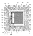
증폭기 레이아웃은 인덕턴스 성분을 저감하기 위해서, 증폭기 트랜지스터 에미터의 패키지 외부의 핀 선단에서 패드까지의 거리가 최단 거리가 되는 위치에 저잡음 증폭기의 회로를 설치하는 것이 바람직하다. 도 3은 그 일례를 나타낸다. 도 3은 도 5에서 설명한 듀얼 밴드 송수신 IC을 예시하고 있다. 참조 번호(301)는 본 발명을 적용한 송수신 IC의 칩이다. 참조 번호(302)는 송수신 IC을 밀봉하는 QFP56 핀이다. 참조 번호(303)는 패키지의 칩 접착면이고, 참조 번호(304)는 패키지 지지재이다. 참조 번호(305)는 본 발명을 적용한 고주파수 대역 차동 저잡음 증폭기(502b)의 레이아웃 장소이다. 또한, 참조 번호(315)는 저주파수 대역 차동 저잡음 증폭기(502a)의 레이아웃 장소이다. In order to reduce the inductance component of the amplifier layout, it is preferable to provide a circuit of a low noise amplifier at a position where the distance from the tip of the pin outside the package of the amplifier transistor emitter to the pad becomes the shortest distance. 3 shows an example thereof. FIG. 3 illustrates the dual band transceiver IC described with reference to FIG. 5.
참조 번호(306, 3l0)는 도 1의 (a)의 트랜지스터(102)의 접지 핀이고, 참조 번호(307, 311)는 트랜지스터(107)의 접지 핀이며, 참조 번호(308, 309)는 각각 저잡음 차동 증폭기(101, 106)의 입력 핀이다. 참조 번호(312)는 고주파수 대역 저잡음 증폭기(502b)의 전원 핀이다.
저주파수 대역 저잡음 증폭기(502a)에서도 마찬가지로, 참조 번호(317)는 도 1의 (b)의 트랜지스터(102)의 접지 핀이고, 참조 번호(320)는 트랜지스터(107)의 접지 핀이며, 참조 번호(318, 319)는 각각 저잡음 차동 증폭기(101, 106)의 입력 핀이다. 참조 번호(3l6)는 저주파수 대역 저잡음 증폭기(502a)의 전원 핀이다. 참조 번호(321)는 바이어스 회로의 전원 핀이며, 참조 번호(322)는 바이어스 회로의 접지 핀이다. 저주파 저잡음 증폭기와 고주파 저잡음 증폭기에서 바이어스 회로의 핀이 공유되고 있다. 참조 번호(323)는 칩 상의 각 패드를 상기 도시된 리드 핀에 접촉시킨 본딩 와이어이다.Similarly in the low frequency band low noise amplifier 502a,
도면에 도시한 바와 같이, 증폭기는 칩 단부면의 중앙 부근에 배치되어, 본딩된다. 이렇게 하면 패드와 핀 간의 본딩 와이어가 짧아진다. 이 실시예에서는 듀얼 밴드를 상정하고 있기 때문에, 본 발명을 적용한 증폭기의 핀은 중앙에서 하단까지 할당된다. 그러나, 접지 핀(306, 307)은 중앙부의 핀에 할당되었다. 이 때문에, 증폭기를 칩의 코너에 배치할 경우보다 인덕턴스 성분이 저감될 수 있다. As shown in the figure, the amplifier is disposed near the center of the chip end face and bonded. This shortens the bonding wire between the pad and the pin. In this embodiment, since dual bands are assumed, the pins of the amplifier to which the present invention is applied are allocated from the center to the bottom. However, ground pins 306 and 307 have been assigned to pins in the middle. For this reason, the inductance component can be reduced more than when the amplifier is placed at the corner of the chip.
지금까지는 증폭기를 갖는 LSI에 대하여 설명하였지만, 본 발명은 증폭기만으로 이루어진 IC에도 적용될 수 있다. 그 경우의 예를 도 4에 나타내었다. 참조 번호(401)는 본 발명을 적용한 차동 증폭기 IC의 칩이다. 참조 번호(402)는 차동 증폭기 IC를 밀봉하는 패키지 TSSOP12 핀이다. 참조 번호(403)는 패키지의 칩 접착면이고, 참조 번호(404)는 패키지 지지재이다. 참조 번호(405, 409)는 트랜지스터(102)의 접지 핀이고, 참조 번호(406, 410)는 트랜지스터(107)의 접지 핀이며, 참조 번호(407, 408)는 각각 차동 증폭기(101, 106)의 입력 핀이다. 참조 번호(411)는 바이어스 회로의 전원 핀이고, 참조 번호(412)는 바이어스 회로의 접지 핀이며, 참조 번호(413, 414)는 차동 증폭기의 출력 핀이고, 참조 번호(415)는 차동 증폭기의 전원 핀이다. 참조 번호(416)는 칩 상의 각 패드로부터 상기 도시된 리드 핀에 접촉된 본딩 와이어이다. Although the LSI having an amplifier has been described so far, the present invention can be applied to an IC composed of only the amplifier. An example of that case is shown in FIG.
도면과 같이 패키지 중앙에 대하여 선대칭으로 핀을 배치하면, 증폭기 트랜지스터 에미터의 패키지 외부의 핀 선단에서 패드까지의 거리가 최단 거리가 된다. 또한, 저잡음 차동 증폭기는 패키지의 전기적 영향을 포함하여도 완전 대칭 회로가 된다. 그러므로, 차동성 특성이 보다 좋은 IC를 기대할 수 있다.When pins are arranged in line symmetry with respect to the center of the package as shown in the figure, the distance from the tip of the pin outside the package of the amplifier transistor emitter to the pad becomes the shortest distance. Low-noise differential amplifiers also become fully symmetrical circuits, including the electrical effects of the package. Therefore, IC with better differential characteristics can be expected.
도 3, 및 도 4는 표 3의 No.2에 나타낸 핀 배치에 준거하였지만, 표 3의 No.3에서 나타낸 핀 배치에 준거할 수도 있다. 3 and 4 are based on the pin arrangement shown in No. 2 of Table 3, but may be based on the pin arrangement shown in No. 3 of Table 3. FIG.
또, 실시예는 저잡음 증폭기를 예로 들어 설명하였지만, 본 발명은 증폭기의 접지 핀의 배치에 관한 것이다. 따라서, 도 1의 (a)에 나타낸 바와 같은 차동 구성의 범용 증폭기에 적용할 수도 있다. In addition, although the embodiment has been described taking a low noise amplifier as an example, the present invention relates to the arrangement of the ground pins of the amplifier. Therefore, the present invention can also be applied to a general-purpose amplifier having a differential configuration as shown in Fig. 1A.
2개의 단위 증폭기를 갖는 본 발명의 차동 증폭기에서는, 제1 단위 증폭기의 접지 핀이 제2 단위 증폭기의 접지 핀 각각에 1 대 1로 인접하게 배치된다. 이에 따라, 트랜지스터의 에미터에서의 인덕턴스가 단일 접지 핀의 인덕턴스의 절반 이하가 된다. 그 결과, 트랜지스터 에미터에 접촉하는 임피던스를 저감할 수 있고, 증폭기의 이득을 향상시킬 수 있다. 또한, 단위 증폭기가 하나의 접지 핀을 갖는 경우, 접지 핀을 입력 핀에 서로 인접하게 배치한다. 이에 따라, 상기와 마찬가지로 임피던스를 감소시킬 수 있어서, 이득을 향상시킬 수 있다. In the differential amplifier of the present invention having two unit amplifiers, the ground pins of the first unit amplifier are disposed one-to-one adjacent to each of the ground pins of the second unit amplifier. As a result, the inductance at the emitter of the transistor is less than half the inductance of the single ground pin. As a result, the impedance in contact with the transistor emitter can be reduced, and the gain of the amplifier can be improved. In addition, when the unit amplifier has one ground pin, the ground pins are disposed adjacent to each other to the input pins. As a result, the impedance can be reduced as described above, so that the gain can be improved.
또한, 송수신 IC와 같은 대규모 IC에 적용하는 경우, 증폭기 트랜지스터의 에미터의 패키지 외부의 핀 선단에서 패드까지의 거리가 최단 거리가 되는 위치에 저잡음 증폭기의 회로를 설치하는 레이아웃으로 조합함으로써, 인덕턴스 저감을 한층 더 실현시킬 수 있다. In addition, when applied to a large-scale IC such as a transceiver IC, inductance reduction is achieved by combining the low noise amplifier circuit in a position where the distance from the tip of the pin outside the package of the emitter of the amplifier transistor to the pad becomes the shortest distance. Can be further realized.
또한, 차동 증폭기만을 포함한 IC에서는, 본 발명에 이하의 2가지 사항을 추가함으로써 이득 향상과, 패키지의 영향도 포함된 대칭 차동 증폭기를 실현할 수 있다. 첫째, 증폭기 트랜지스터 에미터의 패키지 외부의 핀 선단에서 패드까지의 거리가 최단 거리가 되는 위치에 저잡음 증폭기의 회로를 설치한다. 둘째, 패키지에 대하여 대칭으로 핀 배치를 행한다.In addition, in the IC including only the differential amplifier, by adding the following two items to the present invention, a symmetrical differential amplifier including gain improvement and package influence can be realized. First, the circuit of the low noise amplifier is installed at a position where the distance from the tip of the pin outside the package of the amplifier transistor emitter to the pad becomes the shortest distance. Second, pin arrangement is performed symmetrically with respect to the package.
Claims (35)
Applications Claiming Priority (2)
| Application Number | Priority Date | Filing Date | Title |
|---|---|---|---|
| JP2000265982A JP4319339B2 (en) | 2000-08-30 | 2000-08-30 | Semiconductor device |
| JPJP-P-2000-00265982 | 2000-08-30 |
Publications (2)
| Publication Number | Publication Date |
|---|---|
| KR20020018146A KR20020018146A (en) | 2002-03-07 |
| KR100750449B1 true KR100750449B1 (en) | 2007-08-22 |
Family
ID=18753157
Family Applications (1)
| Application Number | Title | Priority Date | Filing Date |
|---|---|---|---|
| KR1020010052874A KR100750449B1 (en) | 2000-08-30 | 2001-08-30 | Semiconductor device |
Country Status (6)
| Country | Link |
|---|---|
| US (1) | US6624509B2 (en) |
| EP (1) | EP1187208A3 (en) |
| JP (1) | JP4319339B2 (en) |
| KR (1) | KR100750449B1 (en) |
| CN (1) | CN1227733C (en) |
| TW (1) | TW516268B (en) |
Families Citing this family (23)
| Publication number | Priority date | Publication date | Assignee | Title |
|---|---|---|---|---|
| JP2002076267A (en) * | 2000-08-22 | 2002-03-15 | Hitachi Ltd | Radio transmitter |
| US20020127992A1 (en) * | 2001-03-08 | 2002-09-12 | Fransis Bert L. | Wideband local oscillator architecture |
| US20020127985A1 (en) * | 2001-03-08 | 2002-09-12 | Fransis Bert L. | Wideband local oscillator architecture |
| US6751470B1 (en) | 2002-04-08 | 2004-06-15 | Nokia Corporation | Versatile RF front-end multiband mobile terminals |
| WO2003094232A1 (en) * | 2002-04-30 | 2003-11-13 | Renesas Technology Corp. | Semiconductor device and electronic device |
| KR100993579B1 (en) | 2002-04-30 | 2010-11-10 | 르네사스 일렉트로닉스 가부시키가이샤 | Semiconductor device and electronic device |
| WO2003094236A1 (en) * | 2002-04-30 | 2003-11-13 | Renesas Technology Corp. | Semiconductor device and radio communication apparatus |
| AU2003234812A1 (en) * | 2002-06-05 | 2003-12-22 | Hitachi Ulsi Systems Co., Ltd. | Semiconductor device |
| KR100499788B1 (en) * | 2002-11-27 | 2005-07-07 | 인티그런트 테크놀로지즈(주) | Integrated Circuit Chip |
| JP4137059B2 (en) * | 2003-02-14 | 2008-08-20 | 株式会社ルネサステクノロジ | Electronic device and semiconductor device |
| TWI225332B (en) * | 2003-05-20 | 2004-12-11 | Mediatek Inc | Multi-band low noise amplifier |
| JP2005006031A (en) * | 2003-06-11 | 2005-01-06 | Sony Corp | Amplifier and receiving circuit |
| KR101014708B1 (en) * | 2003-08-27 | 2011-02-16 | 엘지전자 주식회사 | structure of rotary knob assembly in Washing machine |
| JP4418250B2 (en) * | 2004-02-05 | 2010-02-17 | 株式会社ルネサステクノロジ | High frequency circuit module |
| JP2006073821A (en) * | 2004-09-02 | 2006-03-16 | Sharp Corp | Semiconductor integrated circuit device |
| JP2008218776A (en) * | 2007-03-06 | 2008-09-18 | Renesas Technology Corp | Semiconductor device |
| US8085596B2 (en) * | 2007-09-11 | 2011-12-27 | Micron Technology, Inc. | Reducing noise in semiconductor devices |
| JP5588147B2 (en) * | 2009-10-26 | 2014-09-10 | キヤノン株式会社 | Semiconductor device and printed circuit board mounted with semiconductor device |
| JP5499696B2 (en) | 2009-12-25 | 2014-05-21 | 富士通セミコンダクター株式会社 | Semiconductor device and mounting structure |
| EP3298688A4 (en) * | 2015-05-20 | 2019-01-09 | Wizedsp Ltd. | An ultra-low-power and low-noise amplifier |
| CN106936431B (en) * | 2015-12-30 | 2021-07-20 | 上海贝岭股份有限公司 | High-performance low-noise chip and manufacturing method thereof |
| IT201600086488A1 (en) * | 2016-08-22 | 2018-02-22 | St Microelectronics Srl | SEMICONDUCTOR DEVICE AND CORRESPONDENT PROCEDURE |
| US10880991B2 (en) * | 2018-04-04 | 2020-12-29 | Marvell Asia Pte, Ltd. | Apparatus and methods for enhancing signaling bandwidth in an integrated circuit package |
Citations (3)
| Publication number | Priority date | Publication date | Assignee | Title |
|---|---|---|---|---|
| US5990742A (en) * | 1997-11-26 | 1999-11-23 | Fujitsu Limited | Differential amplifier circuit |
| US5994962A (en) * | 1996-08-29 | 1999-11-30 | Mitsumi Electric Co., Ltd. | Differential amplifier device |
| US5999054A (en) * | 1997-11-19 | 1999-12-07 | Fujitsu Limited | Differential amplifier circuit |
Family Cites Families (7)
| Publication number | Priority date | Publication date | Assignee | Title |
|---|---|---|---|---|
| JP2716005B2 (en) * | 1995-07-04 | 1998-02-18 | 日本電気株式会社 | Wire bond type semiconductor device |
| KR0156334B1 (en) * | 1995-10-14 | 1998-10-15 | 김광호 | Semiconductor chip package having shield bonding wire for high frequency and high density |
| US5789799A (en) * | 1996-09-27 | 1998-08-04 | Northern Telecom Limited | High frequency noise and impedance matched integrated circuits |
| WO1999027646A1 (en) * | 1997-11-21 | 1999-06-03 | Hitachi, Ltd. | High-frequency amplifier circuit device and high-frequency transmission system using the same |
| US6094084A (en) * | 1998-09-04 | 2000-07-25 | Nortel Networks Corporation | Narrowband LC folded cascode structure |
| JP2000299438A (en) * | 1999-04-15 | 2000-10-24 | Hitachi Ltd | Semiconductor integrated circuit |
| JP4018312B2 (en) * | 2000-02-21 | 2007-12-05 | 株式会社ルネサステクノロジ | Wireless communication device |
-
2000
- 2000-08-30 JP JP2000265982A patent/JP4319339B2/en not_active Expired - Fee Related
-
2001
- 2001-05-04 TW TW090110764A patent/TW516268B/en not_active IP Right Cessation
- 2001-07-25 US US09/911,796 patent/US6624509B2/en not_active Expired - Lifetime
- 2001-08-03 EP EP01118714A patent/EP1187208A3/en not_active Withdrawn
- 2001-08-29 CN CNB011258381A patent/CN1227733C/en not_active Expired - Fee Related
- 2001-08-30 KR KR1020010052874A patent/KR100750449B1/en not_active IP Right Cessation
Patent Citations (3)
| Publication number | Priority date | Publication date | Assignee | Title |
|---|---|---|---|---|
| US5994962A (en) * | 1996-08-29 | 1999-11-30 | Mitsumi Electric Co., Ltd. | Differential amplifier device |
| US5999054A (en) * | 1997-11-19 | 1999-12-07 | Fujitsu Limited | Differential amplifier circuit |
| US5990742A (en) * | 1997-11-26 | 1999-11-23 | Fujitsu Limited | Differential amplifier circuit |
Also Published As
| Publication number | Publication date |
|---|---|
| JP4319339B2 (en) | 2009-08-26 |
| KR20020018146A (en) | 2002-03-07 |
| EP1187208A3 (en) | 2011-09-07 |
| CN1227733C (en) | 2005-11-16 |
| JP2002076235A (en) | 2002-03-15 |
| EP1187208A2 (en) | 2002-03-13 |
| US20020053729A1 (en) | 2002-05-09 |
| US6624509B2 (en) | 2003-09-23 |
| CN1340858A (en) | 2002-03-20 |
| TW516268B (en) | 2003-01-01 |
Similar Documents
| Publication | Publication Date | Title |
|---|---|---|
| KR100750449B1 (en) | Semiconductor device | |
| US6847108B2 (en) | Semiconductor integrated circuit | |
| US6275687B1 (en) | Apparatus and method for implementing a low-noise amplifier and mixer | |
| US7274923B2 (en) | Wireless communication system | |
| US6980776B2 (en) | Transceiver apparatus | |
| US6169461B1 (en) | High-frequency oscillating circuit | |
| US7302249B1 (en) | High dynamic range mixer apparatus and balun therefor | |
| US7368996B2 (en) | High frequency power amplifier | |
| US20070202832A1 (en) | Wireless communication system | |
| Imbornone et al. | Fully differential dual-band image reject receiver in SiGe BiCMOS | |
| CN107040219B (en) | Fully integrated low noise amplifier | |
| WO2023157702A1 (en) | High frequency circuit and communication device | |
| JP2007259464A (en) | Semiconductor integrated circuit | |
| JP2004088791A (en) | Semiconductor integrated circuit | |
| WO2000002323A1 (en) | Apparatus and method for implementing a low-noise amplifier | |
| Mheen et al. | A one-chip single-ended 5.8 GHz OFDM receiver front-end using package inductance in SiGe BiCMOS technology |
Legal Events
| Date | Code | Title | Description |
|---|---|---|---|
| A201 | Request for examination | ||
| E701 | Decision to grant or registration of patent right | ||
| GRNT | Written decision to grant | ||
| FPAY | Annual fee payment |
Payment date: 20120724 Year of fee payment: 6 |
|
| FPAY | Annual fee payment |
Payment date: 20130719 Year of fee payment: 7 |
|
| LAPS | Lapse due to unpaid annual fee |