JP7283886B2 - Slicing method and slicing apparatus - Google Patents
Slicing method and slicing apparatus Download PDFInfo
- Publication number
- JP7283886B2 JP7283886B2 JP2018210458A JP2018210458A JP7283886B2 JP 7283886 B2 JP7283886 B2 JP 7283886B2 JP 2018210458 A JP2018210458 A JP 2018210458A JP 2018210458 A JP2018210458 A JP 2018210458A JP 7283886 B2 JP7283886 B2 JP 7283886B2
- Authority
- JP
- Japan
- Prior art keywords
- modified
- modified layer
- wafer
- layer
- workpiece
- Prior art date
- Legal status (The legal status is an assumption and is not a legal conclusion. Google has not performed a legal analysis and makes no representation as to the accuracy of the status listed.)
- Active
Links
Images


Landscapes
- Laser Beam Processing (AREA)
- Mechanical Treatment Of Semiconductor (AREA)
Description
本発明は、スライス方法およびスライス装置に関する。 The present invention relates to a slicing method and a slicing apparatus.
例えばシリコン(Si)、窒化ガリウム(GaN)、シリコンカーバイド(SiC)、サファイア、ダイヤモンドといった硬脆性材料から基板(ウエハ)を製造する方法の一つとして、レーザを用いて硬脆性材料の内部に改質層を形成し、その改質層を境界としてウエハ状に分離する方法がある。 For example, as one method of manufacturing a substrate (wafer) from hard and brittle materials such as silicon (Si), gallium nitride (GaN), silicon carbide (SiC), sapphire, and diamond, a laser is used to modify the interior of the hard and brittle materials. There is a method of forming a modified layer and separating into wafers using the modified layer as a boundary.
例えば特許文献1には、シリコンウエハのスライス工程において、集光レンズでレーザ光の集光点を被加工材の内部に合わせ、そのレーザ光で被加工材を相対的に走査することにより面状の加工領域を形成し、被加工材の内部で発生した熱による膨張・収縮を利用して、加工領域を境界として被加工材の一部を基板として分離する方法が開示されている。
For example, in
しかしながら、上述した従来の方法では、被加工材として硬脆性材料を用いると、楔状の圧入材が圧入された部分の近傍にチッピングを生じさせたり、ウエハが反る方向にモーメントが作用するため、ウエハ自体が割れたりするおそれがある。 However, in the conventional method described above, if a hard and brittle material is used as the workpiece, chipping may occur in the vicinity of the portion where the wedge-shaped press-fitting material is press-fitted, or a moment may act in the direction in which the wafer warps. The wafer itself may crack.
本発明の目的は、被加工材の内部に改質層を形成した後、改質層を境界として被加工材分離する際に生じる不具合を抑制できるスライス方法およびスライス装置を提供することである。 SUMMARY OF THE INVENTION It is an object of the present invention to provide a slicing method and a slicing apparatus capable of suppressing problems that occur when a modified layer is formed inside the workpiece and then the workpiece is separated using the modified layer as a boundary.
本発明の一態様に係るスライス方法は、レーザ発振器からZ方向に出射されたレーザ光をウエハ内部に集光させながらX方向およびY方向に走査して、前記ウエハ内部に複数の改質部が前記X方向および前記Y方向に連なった改質層を形成する改質層形成工程と、熱源により、前記改質層を前記ウエハの融点未満かつ前記改質層の融点以上の温度で加熱することで、前記改質層を溶融し、液状層を形成する改質層溶融工程と、前記液状層を境界として、前記ウエハを分離する分離工程と、を含み、前記改質層は、前記複数の改質部のそれぞれが、前記Z方向において異なる長さおよび位置のばらつきを有することにより凹凸形状を有し、前記改質層を構成する前記改質部それぞれの、前記Z方向における厚みは、前記ウエハの未改質層において、前記改質部の前記Z方向の長さや位置の違いに対応して形成される凹凸形状の、前記Z方向における最高位置と最低位置との高低差よりも大きい。 In a slicing method according to an aspect of the present invention, a laser beam emitted from a laser oscillator in the Z direction is scanned in the X direction and the Y direction while condensing the inside of the wafer to form a plurality of modified portions inside the wafer. a modified layer forming step of forming modified layers continuous in the X direction and the Y direction; and heating the modified layer with a heat source to a temperature lower than the melting point of the wafer and equal to or higher than the melting point of the modified layer. a modified layer melting step of melting the modified layer to form a liquid layer; and a separating step of separating the wafer with the liquid layer as a boundary, wherein the modified layer is formed from the plurality of Each of the modified portions has an uneven shape due to variations in length and position in the Z direction, and the thickness in the Z direction of each of the modified portions constituting the modified layer is In the unmodified layer of the wafer, the height difference between the highest position and the lowest position in the Z direction of the uneven shape formed corresponding to the difference in length and position of the modified portion in the Z direction is larger.
本発明の一態様に係るスライス装置は、Z方向にレーザ光を出射し、ウエハ内部に集光させながらX方向およびY方向に走査して、前記ウエハ内部に複数の改質部が前記X方向および前記Y方向に連なった改質層を形成するレーザ発振器と、前記改質層を前記ウエハの融点未満かつ前記改質層の融点以上の温度で加熱することで、前記改質層を溶融し、液状層を形成する熱源と、前記液状層を境界として、前記ウエハを分離する分離部と、を含み、前記改質層は、前記複数の改質部のそれぞれが、前記Z方向において異なる長さおよび位置のばらつきを有することにより凹凸形状を有し、前記改質層を構成する前記改質部それぞれの、前記Z方向における厚みは、前記ウエハの未改質層において、前記改質部の前記Z方向の長さや位置の違いに対応して形成される凹凸形状の、前記Z方向における最高位置と最低位置との高低差よりも大きい。 A slicing apparatus according to an aspect of the present invention emits a laser beam in the Z direction and scans in the X direction and the Y direction while concentrating the laser beam inside the wafer to form a plurality of modified portions inside the wafer in the X direction. and a laser oscillator for forming a modified layer continuous in the Y direction; a heat source for forming a liquid layer; and a separating section for separating the wafer with the liquid layer as a boundary, wherein the modified layer has a plurality of modified sections each having a different length in the Z direction. The thickness in the Z direction of each of the modified portions constituting the modified layer has an uneven shape due to variations in thickness and position, and the thickness in the Z direction is the same as that of the modified portion in the unmodified layer of the wafer. It is larger than the height difference between the highest position and the lowest position in the Z direction of the uneven shape formed corresponding to the difference in length and position in the Z direction.
本発明によれば、被加工材の内部に改質層を形成した後、改質層を境界として被加工材を分離する際に生じる不具合を抑制することができる。 ADVANTAGE OF THE INVENTION According to this invention, after forming a modified layer in the inside of a to-be-processed material, the trouble which arises when separating a to-be-processed material using a modified layer as a boundary can be suppressed.
以下、本発明の実施の形態について、図面を参照しながら説明する。なお、各図において、共通する構成要素については同一符号を付し、それらの構成要素については適宜説明を省略する。 BEST MODE FOR CARRYING OUT THE INVENTION Hereinafter, embodiments of the present invention will be described with reference to the drawings. In addition, in each figure, the same code|symbol is attached|subjected about a common component, and description is abbreviate|omitted suitably about those components.
本発明の実施の形態に係るレーザ加工装置(改質層形成装置)100の構成について説明する。図1は、本実施の形態に係るスライス装置100の模式図である。
A configuration of a laser processing apparatus (modified layer forming apparatus) 100 according to an embodiment of the present invention will be described. FIG. 1 is a schematic diagram of a
レーザ加工装置100は、固定テーブル2、駆動ステージ3、レーザ発振器4、ミラー6、およびレンズ7を有する。
A
被加工材1は、例えば窒化ガリウム(硬脆性材料の一例。以下、GaNともいう)で構成され、内部に、後述の改質層8が形成される加工対象の部材である。被加工材1としては、例えば、直径が2インチ、厚みが400μmであるものが好ましいが、直径および厚みは上記値に限定されるものではなく、400μmより厚いインゴット材を用いてもよいし、2インチより大きい直径のインゴット材を用いてもよい。
The
固定テーブル2は、例えば真空吸着により被加工材1を固定する。なお、固定テーブル2としては、後述する駆動ステージ3の駆動による被加工材1の位置ズレが生じないものを用いる。
The fixed table 2 fixes the
駆動ステージ3は、X軸、Y軸、Z軸の各方向への駆動、およびθ方向に回転可能である。また、駆動ステージ3は、被加工材1に対するレーザ光5の相対位置を制御することができる。
The
レーザ発振器4は、被加工材1に対して、例えば直径約4mmの直線偏光であるレーザ光5を出射する。例えば、レーザ光5は、50%以上の透過率を有する波長(例えば、波長532nm)であり、パルス幅が0.2ピコ秒以上かつ100ピコ秒以下(例えば、15ピコ秒)であり、最大出力50Wのピコ秒レーザである。また、レーザ光5の最大繰返し周波数は1MHzである。
A
また、レーザ発振器4は、駆動ステージ3との制御信号(図1に示す破線の両矢印)のやりとりにより、レーザ光5のON/OFFを制御することができる。
In addition, the
なお、透過率の測定には、例えば、積分球付き分光光度計(日本分光株式会社製、V7100。図示略)を用いる。透過率とは、レーザ発振器4から出射された全光量に対する、被加工材1を透過した光の光量(光度計で受光された光量)の比である。
For the transmittance measurement, for example, a spectrophotometer with an integrating sphere (V7100 manufactured by JASCO Corporation; not shown) is used. The transmittance is the ratio of the amount of light transmitted through the workpiece 1 (the amount of light received by the photometer) to the total amount of light emitted from the
ミラー6は、レーザ発振器4から出射されたレーザ光5を90%以上反射させ、レンズ7へ送ることができる。ミラー6としては、例えば、波長532nmのレーザ光5を高い反射率で反射する誘電多層膜ミラーを用いることができる。
The
レンズ7は、レーザ光5を集光する際(レーザ光5が被加工材1を透過するとき)に生じる収差を加工深さに応じて最適な収差量に補正することが可能なレンズである。
The
レンズ7を透過したレーザ光5aの集光点A(レーザ光5aの先端部分)は、被加工材1の内部において、被加工材1の表面(図中の上面)から距離B離れた位置に調整されている。
A focal point A (tip of the
レンズ7としては、例えば、波長532nmのレーザ光5を透過させる顕微鏡用の収差補正環付きであって、開口数(Numerical Aperture:NA)が0.7であり、焦点距離が4mmのレンズを用いることができる。
As the
また、レンズ7のうち少なくともレーザ光5を入射させる面は、レーザ光5が被加工材1に対して少なくとも50%以上の透過率を有するように、鏡面加工が施されている。
At least the surface of the
改質層8は、集光点Aの近傍において窒化ガリウムの改質成分で形成され、主にGaNが分解されて生成されたガリウム(Ga)、ガリウムの二量体およびGaxNyクラスタにより形成される。改質層8を形成するにあたっては改質層8の厚みが20μm以下となるように調整されるが、駆動ステージ3の精度および固定テーブル2(被加工材1)の面精度等により、改質層8は、凹凸を有した形状となる。
The modified
次に、図1に示したレーザ加工装置100の動作について、図2A、図2B、図3A、図3B、および図3Cを用いて説明する。図2A、図2B、図3A、図3B、および図3Cは、レーザ加工装置100による改質層形成動作を説明する模式図である。
Next, operations of the
レーザ光5aは、上述したように、被加工材1に対する50%以上の透過率を有するため、集光点Aの近傍に減衰の小さい状態で集光される。ここでは例として、集光点Aと被加工材1の表面との間の距離Bを、被加工材1の厚み400μmの1/2、すなわち200μmに設定する。
Since the
レンズ7の収差補正環は、被加工材1の厚みに応じて調整されるため、レーザ光5aは、集光点Aにおいて最も絞られた状態となる。上述したとおりレーザ光5はピコ秒レーザであるため、多光子吸収加工により、集光点Aにおいて主に下記式(1)の反応が生じ、改質層8が形成される。
2GaN→2Ga+N2・・・(1)
Since the aberration correction ring of the
2GaN→2Ga+N 2 (1)
材料分析結果によれば、改質層8においては、主にGaが生成され、Ga以外にもGa二量体、GaxNyクラスタが形成されることが分かっている。Gaは融点Tm=29.8℃の液体金属と呼ばれるものである。
According to the material analysis results, it is known that Ga is mainly generated in the modified
固定テーブル2に固定された被加工材1は、駆動ステージ3の駆動によりレーザ光5aに対して相対的に移動する。これにより、面状の改質層8が形成される。
A
図2Aおよび図2Bは、それぞれ、改質層形成動作における被加工材1の移動方向(レーザ光5aの走査方向と言ってもよい)の一例を示している。矢印E1、E2はレーザパルスを照射しながら走査する方向を示しており、実際には図2Cに示すようになる。
FIGS. 2A and 2B each show an example of the moving direction of the workpiece 1 (which may also be called the scanning direction of the
図2Aの各矢印E1に示すように、被加工材1を、X軸方向においてライン間隔D1の分だけずらしながら、Y軸方向において所定の向きへの移動と逆向きへの移動とを交互に繰り返すことにより、改質層8を形成してもよい。
As indicated by each arrow E1 in FIG. 2A, the
または、図2Bの各矢印E2に示すように、被加工材1を、X軸方向においてライン間隔D1の分だけずらしながら、Y軸方向において同じ向きに移動させることを繰り返すことにより、改質層8を形成してもよい。 Alternatively, as shown by arrows E2 in FIG. 2B, the material to be processed 1 is moved in the same direction in the Y-axis direction while being shifted by the line spacing D1 in the X-axis direction. 8 may be formed.
また、Y軸方向におけるレーザ照射パルス間隔D2は、図2Cに示した走査方向に隣あうレーザパルスの間隔を示し、レーザ発振器4の繰り返し周波数Fおよび駆動ステージ3の走査速度Vにより決まる。例えば、レーザ照射パルス間隔D2は、以下の式(2)で算出される値となる。
D2=V/F・・・(2)
A laser irradiation pulse interval D2 in the Y-axis direction indicates an interval between adjacent laser pulses in the scanning direction shown in FIG. For example, the laser irradiation pulse interval D2 is a value calculated by the following formula (2).
D2=V/F (2)
例えば、繰り返し周波数が1000kHzであり、走査速度が1000mm/sである場合、1μmごとに、集光点A近傍に改質層8が形成される。ライン間隔D1およびレーザ照射パルス間隔D2はともに、レーザ光5の集光スポット径以下(例えば、1μm以下)であることが好ましいが、集光スポット径は光学系によって異なるため、集光スポット径以下に限定されない。
For example, when the repetition frequency is 1000 kHz and the scanning speed is 1000 mm/s, the modified
図3A~図3Cは、それぞれ、改質層形成動作時の被加工材1の断面を示している。
3A to 3C each show a cross section of the
図3Aは、被加工材1の端部における改質層8の形成状態を示している。9xは、X方向のエネルギ密度プロファイルを示し、9zは、Z(深さ)方向のエネルギ密度プロファイルを示す。
FIG. 3A shows the formation state of the modified
X方向およびZ方向のどちらに関しても、レーザ光5aの集光点近傍において急激にエネルギ密度が上昇することにより、多光子吸収と呼ばれる現象が発生する。このため、集光点以外ではレーザ光5aは透過するのに対し、エネルギ密度が高い集光点でのみレーザ光が吸収されることで、被加工材1の内部に改質部8aが形成される。改質部8aは、Y軸方向にレーザ光5aが走査され、線状に形成される。
In both the X direction and the Z direction, a phenomenon called multiphoton absorption occurs due to the sudden increase in energy density in the vicinity of the focal point of the
図3Aに示した改質部8aの形成の後、図3Bに示すように、X軸方向にライン間隔D1の分ずれた位置においてY軸方向にレーザ光5aを複数回走査することで、連続した改質部8bが形成される。そして、最終的には、図3Cに示すように、被加工材1の全面にわたって面状の改質層8が形成される。
After forming the modified
このようにして形成された改質層8は、駆動ステージ3の駆動精度や固定テーブル2(被加工材1)の面精度の影響を受けるため、Z方向に集光点がばらつきながら形成された形状となる。
The modified
図3Cでは例として、改質層8を、楕円状の改質部8a、8bが連なった形状として図示しているが、実際に形成される改質層8では、レーザ光5aの入射側が、レーザ光5aの出射側よりも、平坦な形状となる。これは、レーザ光5aの入射側の形状が、上下動が少ない集光点の位置によって決まる一方で、レーザ光5aの出射側では、集光点で加工に用いられなかった漏れ光が加工閾値を超える範囲で改質が進むため、改質範囲を規定することが困難であるためである。
As an example in FIG. 3C, the modified
図4Aおよび図4Bは、改質層8が形成された被加工材1の断面を示す模式図である。図4Aは、レーザ走査方向(主走査方向と言ってもよい。例えば、Y軸方向)に対して垂直な副走査方向(例えば、X軸方向)の断面を示している。図4Bは、レーザ走査方向に平行なY軸方向の断面を示している。
4A and 4B are schematic diagrams showing cross sections of the
改質層8は、線状の改質部8a、8b(図3A、図3B参照)が連なって形成されるため、図4Aに示すように、レーザ走査方向と垂直なX軸方向では、Z方向のばらつきの有無や程度に関わらず、凹凸の大きい形状が得られる。また、図4Bに示すように、レーザ走査方向と平行なY軸方向では、駆動ステージ3の精度や固定テーブル2の面精度の影響が支配的な凹凸の小さい形状が得られる。
Since the modified
次に、改質層8を形成した被加工材1を分離する分離装置200(本発明のスライス装置の一例)について、図5を用いて説明する。図5は、本実施の形態に係る分離装置200の模式図である。
Next, a separating apparatus 200 (an example of the slicing apparatus of the present invention) for separating the
分離装置200は、分離治具11(分離部の一例)および加熱装置12(加熱部の一例)を有する。
The
粘着シート10は、両面に粘着力を有する。この粘着力は、120℃(熱剥離温度To)以上に加熱された場合に失われる。粘着シート10としては、例えば、ダイシングテープを用いることができる。
The
分離治具11は、X軸方向、Y軸方向、Z軸方向に水平移動でき、θ方向(図1参照)に回転できる。また、分離治具11は、温度測定機能を有し、測定した温度を後述の加熱装置12にフィードバックすることができる。
The
加熱装置12は、被加工材1を加熱する接触式の熱源(例えば、ホットプレートなど)である。加熱装置12は、分離治具11に測定された温度に基づいて、改質層8の融点Tn以上、粘着シート10の熱剥離温度To未満になるように、加熱温度を制御する。なお、改質層8の主成分はガリウム(Ga)であることから、改質層8の融点Tn=Gaの融点Tmとみなしてよい。
The
次に、図5に示した分離装置の動作について、図6A、図6Bを用いて説明する。図6Aおよび図6Bは、分離装置による被加工材分離動作を説明する模式図である。 Next, the operation of the separation device shown in FIG. 5 will be described with reference to FIGS. 6A and 6B. 6A and 6B are schematic diagrams for explaining the separation operation of the workpiece by the separation device.
改質層8は、加熱装置12により融点Tn以上に加熱されると、溶融する。このときに、分離治具11を用いて、改質層8が形成されたXY面と略平行な方向へ荷重を作用させ、改質層8を境界として、被加工材1の上部ウエハ(以下、単に、上部という)1aと被加工材1の下部ウエハ(以下、単に、下部という)1bとを、XY面と略平行な方向にずらす。これにより、被加工材1は、上部1aと下部1bとに分離する。
When the modified
また、加熱装置12により熱剥離温度To以上に加熱されることで、粘着シート10の粘着力は失われる。これにより、分離後の上部1aおよび下部1bは、分離治具11から剥離することができる。
Moreover, the adhesive force of the
図6Aは、上部1aと下部1bとをC1方向(レーザ走査方向に垂直なX軸方向)にずらした場合を示している。上述したとおり、加熱装置12の加熱により改質層8は溶融するが、改質層8周縁の未改質部(GaN部と言ってもよい)には、C1方向に対して垂直な方向(Z方向)に凹凸部分が残存する。よって、図6Aに示すように、上部1aと下部1bとをC1方向にずらす場合、上部1aの凹凸部分と下部1bの凹凸部分とが干渉する。したがって、上部1aと下部1bとを十分にずらすことができず、被加工材1を上部1aと下部1aとに分離することができない。
FIG. 6A shows the case where the
一方、図6Bは、上部1aと下部1bとをC2方向(レーザ走査方向と平行なY軸方向)にずらした場合を示している。レーザ走査方向には凹凸部分が少なく、凹凸部分があったとしても、駆動ステージ3の精度や固定テーブル2の面精度に起因する緩やかな凹凸形状である。よって、図6Bに示すように、上部1aと下部1bとをC2方向にずらす場合、上部1aの凹凸部分と下部1bの凹凸部分との干渉は生じにくい。すたがって、被加工材1を上部1aと下部1bとに分離することができる。
On the other hand, FIG. 6B shows the case where the
また、図7に示すように、上部1aの未改質層の表面粗さ(Z方向の長さ)をRza、下部1bの未改質層の表面粗さ(Z方向の長さ)をRzb、改質層8の厚み(Z方向の長さ)をFとした場合、F>RzaかつF>Rzbを満たすように改質層8を形成する。さらには、表面粗さRza、Rzbに比べて、厚みFが10%以上大きい改質層8を形成することが好ましい。これにより、上述した凹凸部分による干渉の影響を低減することができ、より安定した分離を実現できる。
Further, as shown in FIG. 7, Rza is the surface roughness (length in the Z direction) of the unmodified layer of the
例えば、厚みFが約10μmであり、表面粗さRza、Rzbがそれぞれ約20μm程度である場合、上部1aと下部1bとを分離することは困難となる。よって、その場合、厚みFが20μmよりも大きくなるように改質層8を形成することが好ましい。このような厚みFを得るためには、集光点近傍でエネルギ密度が加工閾値を超える領域を広げる必要がある。よって、レーザ光5aのパワーを大きくしたり、NA(開口数)が少し小さいレンズを用いたりすればよい。
For example, when the thickness F is approximately 10 μm and the surface roughnesses Rza and Rzb are each approximately 20 μm, it becomes difficult to separate the
次に、分離時の傾きについて説明する。 Next, the inclination at the time of separation will be explained.
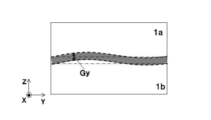
図9に改質層を形成した被加工材1の斜視図を示す。改質層厚みFにおいて、XZ平面において隣り合うレーザ走査間が接続されている部分の厚みをGxとし、YZ平面において隣り合うレーザ走査間が接続されている部分の厚みをGyとする。また、X方向の被加工材1のサイズをW1、Y方向の被加工材1のサイズをW2とする。
FIG. 9 shows a perspective view of the
図10Aは、被加工材1の上部1aおよび下部1bが水平方向に回転した状態を真上から見た模式図である。図10Bは、被加工材1のXZ平面における端面が回転する前の状態を示す模式図である。図10Cは、図10Bに示した端面が回転した後の状態を示す模式図である。
FIG. 10A is a schematic diagram showing a state in which the
図10Cに示すように上部1aに対して下部1bが距離Hずれることにより、図10Aに示すように上部1aおよび下部1bが角度θ1回転する。これにより、図10Cに示す衝突点15が生じ、これ以上回転できない状態となる。角度θ1は、以下の式(3)で表すことができる。
θ1=tan-1(H/W2)≒H/W2[rad]・・・(3)
As shown in FIG. 10C, the displacement of the
θ1=tan −1 (H/W2)≈H/W2 [rad] (3)
図11Aは、上部1aおよび下部1bがZ方向に傾いた状態を示す模式図である。図11Bは、被加工材1のYZ平面における端面が傾く前の状態を示す模式図である。図11Cは、図11Bに示した端面が傾いた後の状態を示す模式図である。
FIG. 11A is a schematic diagram showing a state in which the
図11Aに示すように上部1aに対して下部1bが図11Cに示す角度θ2傾くことにより、図11Cに示す衝突点16が生じ、これ以上傾くことができない状態となる。角度θ2は、以下の式(4)で表すことができる。
θ2=tan-1(Gy/W2)≒Gy/W2[rad]・・・(4)
As shown in FIG. 11A, the
θ2=tan −1 (Gy/W2)≈Gy/W2 [rad] (4)
例えば、厚みGx=Gy=5μm、H=10μm、W1=W2=50mmである場合、 θ1=H/W2=10/(50×1000)=0.2mrad
θ2=Gy/W2=5/(50×1000)=0.1mrad
となる。
For example, when thickness Gx=Gy=5 μm, H=10 μm, W1=W2=50 mm, θ1=H/W2=10/(50×1000)=0.2 mrad
θ2=Gy/W2=5/(50×1000)=0.1 mrad
becomes.
つまり、図10Bに示す状態と図10Cに示す状態との間の状態、または、図11Bに示す状態と図11Cに示す状態との間の状態であれば、上部1aと下部1bの相対位置を変更することは可能であり、ウエハを分離することができる。よって、この状態を略平行と定義することができる。
10B and 10C, or between the state shown in FIG. 11B and the state shown in FIG. 11C, the relative positions of the
上記説明では、改質層8が1つである場合を例に挙げて説明したが、改質層8は複数あってもよい。以下、この場合について、図8を用いて説明する。図8は、複数の改質層8が形成された被加工材1の断面を示す模式図である。
In the above description, the case where there is one modified
図8において、押さえ部13は、被加工材1をスライスした後のウエハ1c、1d、1e、1f、1gのどの高さにも合わせることができ、C方向の分離荷重に負けない強度を有する。
In FIG. 8, the
図8では、例として、ウエハ1cを分離するために、押さえ部13をウエハ1dの高さに調整した場合を示している。C方向に荷重を作用させる際に、ウエハ1より下方のウエハ1d~1gのズレを抑制することにより、C方向への荷重がウエハ1cとウエハ1dとの間の改質層の分離に作用するため、ウエハ1cのみを分離することができる。
FIG. 8 shows, as an example, the case where the holding
ウエハ1cを分離した後、ウエハ1dの表面を研磨する。その後、再度粘着シート10により、残りの被加工材1を固定し、押さえ部13の位置をウエハ1eの高さに変更する。これにより、ウエハ1dを分離することができる。
After separating the wafer 1c, the surface of the wafer 1d is polished. After that, the remaining
なお、ウエハ1e~1gに対しても上述した動作を繰り返すことにより、ウエハ1e~1gを分離することができる。分離後のウエハ1c~1gは、後工程で研磨され、改質層8が除去される。これにより、GaNウエハとして用いることができるようになる。
By repeating the above operation for the
以上説明したように、本実施の形態は、レーザ光5aの集光により形成された被加工材1の改質層8を、被加工材1の融点未満かつ改質層8の融点以上の温度で加熱することにより、改質層8を溶融させ、溶融した改質層8を境界として、被加工材1を分離することを特徴とする。
As described above, according to the present embodiment, the modified
これにより、本実施の形態では、被加工材の内部に改質層を形成した後、改質層を境界として被加工材を分離する際に生じる不具合(例えば、チッピング、クラック、割れなど)を抑制できる。したがって、分離時の歩留りを向上させることができる。また、後工程において研磨量を低減できるので、材料ロスの低減も期待できる。 As a result, in the present embodiment, after the modified layer is formed inside the work material, problems (for example, chipping, cracking, cracking, etc.) that occur when the work material is separated with the modified layer as a boundary are eliminated. can be suppressed. Therefore, the yield at the time of separation can be improved. In addition, since the polishing amount can be reduced in the post-process, reduction of material loss can be expected.
なお、本発明は、上記実施の形態の説明に限定されず、その趣旨を逸脱しない範囲において種々の変形が可能である。以下、各変形例について説明する。 The present invention is not limited to the description of the above embodiments, and various modifications are possible without departing from the spirit of the present invention. Each modification will be described below.
[変形例1]
実施の形態では、Y軸方向の直線走査を例に挙げて説明したが、これに限定されない。例えば、X軸方向の直線走査、θ軸回りの回転走査、θ軸の回転中心から偏芯させた位置に被加工材1を設置した円弧走査などを用いてもよい。なお、X軸走査を用いる場合、上記実施の形態と同様に被加工材1の分離が可能であるが、回転走査または円弧走査を用いる場合では、被加工材1を分離させる際に、回転方向または円弧方向に分離荷重を作用させる必要がある。
[Modification 1]
Although linear scanning in the Y-axis direction has been described as an example in the embodiments, the present invention is not limited to this. For example, linear scanning in the X-axis direction, rotational scanning around the .theta.-axis, arc scanning in which the
[変形例2]
実施の形態では、加熱装置12として、接触式の熱源を用いる場合を例に挙げて説明した、加熱装置12は非接触式の熱源であってもよい。例えば、非接触式の熱源として、被加工材1に対して80%以上の透過率を有し、改質層8が50%以上の吸収性を示す光を発する光源(例えば、IRヒータ、ハロゲンランプなど)を用いてもよい。この場合も、実施の形態と同様に、改質部に析出したGaを加熱しながらの分離が可能となる。
[Modification 2]
In the embodiment, the case where a contact heat source is used as the
[変形例3]
実施の形態では、加熱装置12の加熱温度が、改質層8の融点Tn以上、かつ、粘着シート10の熱剥離温度To未満である場合を例に挙げて説明したが、これに限定されない。例えば、粘着シート10を用いない場合(例えば、支持基板上に固定して剥離させない場合や、真空吸着などにより固定する場合など)には、加熱温度を、改質層8の融点Tn以上、かつ、被加工材1(GaN基板)の融点未満に設定すればよい。
[Modification 3]
In the embodiment, the case where the heating temperature of the
[変形例4]
実施の形態では、被加工材1として、直径が2インチであり、厚みが400μmであり、材質が窒化ガリウムである材料を用いる場合を例に挙げて説明したが、直径、厚み、および材質は、これに限定されない。被加工材1の材質は、例えば、シリコン基板、サファイア基板、サファイア基板上にGaN層をエピタキシャル成長させた基板、ヒ化ガリウム(GaAs)基板、リン化インジウム(InP)基板、窒化アルミニウムガリウム(AlGaN)/GaN基板、SiC基板、SiC基板上にGaN層をエピタキシャル成長させた基板、ダイヤモンドなどであってもよい。すなわち、レーザ光が透過し、改質層を形成可能な材料であれば適用可能である。ただし、改質層の融点が低い材質(例えば、GaN)が好適である。
[Modification 4]
In the embodiment, a case where a material having a diameter of 2 inches, a thickness of 400 μm, and a material made of gallium nitride is used as the
[変形例5]
実施の形態では、レーザ発振器4から発振されるレーザ光5の波長が532nmである場合を例に挙げて説明したが、レーザ光5の波長は、これに限定されず、被加工材1に対して透過率を有する波長であればよい。ただし、短い波長の方が、被加工材1内部の集光点Aの厚み方向および水平方向の寸法が小さくなり、加工性が向上するため、好適である。
[Modification 5]
In the embodiment, the case where the wavelength of the
[変形例6]
実施の形態では、レーザ光5のパルス幅が0.2ピコ秒以上かつ100ピコ秒以下であり、レーザ光5の最大繰返し周波数が1MHzである場合を例に挙げて説明したが、これに限定されない。例えば、レーザ光5のパルス幅は、1フェムト秒(fs)以上かつ1ナノ秒(ns)以下の範囲であって、多光子吸収による内部加工が可能となるものであればよい。レーザ光5の繰り返し周波数は、被加工材1とレーザ光5との相互作用に起因する加工性と、生産性との関係から、レーザ発振器4が発振可能な10MHz以下の範囲から選択されればよい。
[Modification 6]
In the embodiment, the pulse width of the
[変形例7]
実施の形態では、レンズ7の開口数が0.7である場合を例に挙げて説明したが、これに限定されず、0.4以上かつ0.95以下であればよい。ただし、集光点Aの径を小さくするために、レンズ7の開口数は大きい方が好ましい。レンズ7としては、集光点Aのエネルギ密度を高くできるため、収差補正機能付レンズを用いることが望ましいが、これに限定されず、例えば位相変調素子やレンズなどにより、予め収差補正を加えてもよい。
[Modification 7]
In the embodiment, the case where the numerical aperture of the
[変形例8]
また、実施の形態で説明した改質層形成動作および被加工材分離動作は、例えばミラー、回折光学素子または位相変調素子を用いて、レーザ光5を被加工材1の複数部分に同時に照射し、被加工材1を加工する場合にも適用できる。その場合、加工時間を短縮できるので、より生産性が向上する。
[Modification 8]
Further, the modified layer forming operation and the work material separation operation described in the embodiment are performed by simultaneously irradiating a plurality of portions of the
本発明は、レーザを用いて硬脆性材料の内部に改質層を形成し、その改質層を境界としてウエハ状に分離する技術全般に適用できる。 INDUSTRIAL APPLICABILITY The present invention can be applied to general techniques for forming a modified layer inside a hard and brittle material using a laser and separating the material into wafers with the modified layer as a boundary.
1 被加工材
1a 被加工材1の上部ウエハ
1b 被加工材1の下部ウエハ
1c、1d、1e、1f、1g ウエハ
2 固定テーブル
3 駆動ステージ
4 レーザ発振器
5、5a レーザ光
6 ミラー
7 レンズ
8 改質層
8a、8b 改質部
10 粘着シート
11 分離治具
12 加熱装置
13 押さえ部
15、16 衝突点
100 レーザ加工装置
200 分離装置
REFERENCE SIGNS
Claims (5)
熱源により、前記改質層を前記ウエハの融点未満かつ前記改質層の融点以上の温度で加熱することで、前記改質層を溶融し、液状層を形成する改質層溶融工程と、
前記液状層を境界として、前記ウエハを分離する分離工程と、を含み、
前記改質層は、前記複数の改質部のそれぞれが、前記Z方向において異なる長さおよび位置のばらつきを有することにより凹凸形状を有し、
前記改質層を構成する前記改質部それぞれの、前記Z方向における厚みは、前記ウエハの未改質層において、前記改質部の前記Z方向の長さや位置の違いに対応して形成される凹凸形状の、前記Z方向における最高位置と最低位置との高低差よりも大きい、
スライス方法。 A laser beam emitted in the Z direction from a pulse laser oscillator is condensed and irradiated inside the wafer to generate a modified portion, and the laser beam is scanned in the X and Y directions to form a plurality of laser beams inside the wafer. a modified layer forming step of forming a modified layer in which modified portions are continuous in the X direction and the Y direction;
A modified layer melting step of heating the modified layer to a temperature lower than the melting point of the wafer and equal to or higher than the melting point of the modified layer by a heat source to melt the modified layer to form a liquid layer;
a separation step of separating the wafer with the liquid layer as a boundary;
The modified layer has an uneven shape in which each of the plurality of modified portions has different lengths and positional variations in the Z direction,
The thickness in the Z direction of each of the modified portions constituting the modified layer is formed corresponding to the difference in the length and position of the modified portion in the Z direction in the unmodified layer of the wafer. larger than the height difference between the highest position and the lowest position in the Z direction of the uneven shape
slicing method.
請求項1に記載のスライス方法。 In the separation step, the wafer is separated in a direction parallel to the scanning direction of the laser beam.
The slicing method according to claim 1.
請求項1または2に記載のスライス方法。 The pulse width of the laser light is 0.2 picoseconds or more and 100 picoseconds or less.
The slicing method according to claim 1 or 2.
請求項1から3のいずれか1項に記載のスライス方法。 The laser light has a wavelength at which the transmittance of the wafer is 50% or more,
The slicing method according to any one of claims 1 to 3.
前記改質層を前記ウエハの融点未満かつ前記改質層の融点以上の温度で加熱することで、前記改質層を溶融し、液状層を形成する熱源と、
前記液状層を境界として、前記ウエハを分離する分離部と、を含み、
前記改質層は、前記複数の改質部のそれぞれが、前記Z方向において異なる長さおよび位置のばらつきを有することにより凹凸形状を有し、
前記改質層を構成する前記改質部それぞれの、前記Z方向における厚みは、前記ウエハの未改質層において、前記改質部の前記Z方向の長さや位置の違いに対応して形成される凹凸形状の、前記Z方向における最高位置と最低位置との高低差よりも大きい、
スライス装置。
A pulsed laser beam is emitted in the Z direction, and the inside of the wafer is focused and irradiated to generate a modified portion, and the laser beam is scanned in the X and Y directions to form a plurality of modified portions inside the wafer. a laser oscillator that forms a modified layer that is continuous in the X direction and the Y direction;
a heat source that melts the modified layer by heating the modified layer to a temperature lower than the melting point of the wafer and higher than or equal to the melting point of the modified layer to form a liquid layer;
a separating unit that separates the wafer with the liquid layer as a boundary;
The modified layer has an uneven shape in which each of the plurality of modified portions has different lengths and positional variations in the Z direction,
The thickness in the Z direction of each of the modified portions constituting the modified layer is formed corresponding to the difference in the length and position of the modified portion in the Z direction in the unmodified layer of the wafer. larger than the height difference between the highest position and the lowest position in the Z direction of the uneven shape
slicing device.
Priority Applications (2)
| Application Number | Priority Date | Filing Date | Title |
|---|---|---|---|
| CN201910097785.1A CN110102882A (en) | 2018-02-01 | 2019-01-31 | Dicing method and slicing device |
| US16/263,382 US20190232433A1 (en) | 2018-02-01 | 2019-01-31 | Slicing method and slicing apparatus |
Applications Claiming Priority (2)
| Application Number | Priority Date | Filing Date | Title |
|---|---|---|---|
| JP2018016347 | 2018-02-01 | ||
| JP2018016347 | 2018-02-01 |
Publications (2)
| Publication Number | Publication Date |
|---|---|
| JP2019134155A JP2019134155A (en) | 2019-08-08 |
| JP7283886B2 true JP7283886B2 (en) | 2023-05-30 |
Family
ID=67546605
Family Applications (1)
| Application Number | Title | Priority Date | Filing Date |
|---|---|---|---|
| JP2018210458A Active JP7283886B2 (en) | 2018-02-01 | 2018-11-08 | Slicing method and slicing apparatus |
Country Status (1)
| Country | Link |
|---|---|
| JP (1) | JP7283886B2 (en) |
Families Citing this family (2)
| Publication number | Priority date | Publication date | Assignee | Title |
|---|---|---|---|---|
| JPWO2021193060A1 (en) * | 2020-03-24 | 2021-09-30 | ||
| EP4163046A1 (en) * | 2021-10-07 | 2023-04-12 | Denso Corporation | Method for manufacturing wafers |
Citations (6)
| Publication number | Priority date | Publication date | Assignee | Title |
|---|---|---|---|---|
| JP2003303743A (en) | 2002-04-08 | 2003-10-24 | Matsushita Electric Ind Co Ltd | Manufacturing method of nitride semiconductor device and its substrate |
| JP2013158779A (en) | 2012-02-01 | 2013-08-19 | Shin Etsu Polymer Co Ltd | Processed monocrystal member and method for manufacturing the same |
| JP2015119076A (en) | 2013-12-19 | 2015-06-25 | 信越ポリマー株式会社 | Internal processing layer formation single crystal member and manufacturing method therefor |
| JP2016043558A (en) | 2014-08-22 | 2016-04-04 | アイシン精機株式会社 | Manufacturing method of base board, cutting method of processed object and laser processor |
| JP2017069510A (en) | 2015-10-02 | 2017-04-06 | 日亜化学工業株式会社 | Semiconductor element manufacturing method |
| JP2017183600A (en) | 2016-03-31 | 2017-10-05 | パナソニックIpマネジメント株式会社 | Slice method and slice device |
Family Cites Families (1)
| Publication number | Priority date | Publication date | Assignee | Title |
|---|---|---|---|---|
| JPH06268051A (en) * | 1993-03-10 | 1994-09-22 | Mitsubishi Electric Corp | Wafer stripper |
-
2018
- 2018-11-08 JP JP2018210458A patent/JP7283886B2/en active Active
Patent Citations (6)
| Publication number | Priority date | Publication date | Assignee | Title |
|---|---|---|---|---|
| JP2003303743A (en) | 2002-04-08 | 2003-10-24 | Matsushita Electric Ind Co Ltd | Manufacturing method of nitride semiconductor device and its substrate |
| JP2013158779A (en) | 2012-02-01 | 2013-08-19 | Shin Etsu Polymer Co Ltd | Processed monocrystal member and method for manufacturing the same |
| JP2015119076A (en) | 2013-12-19 | 2015-06-25 | 信越ポリマー株式会社 | Internal processing layer formation single crystal member and manufacturing method therefor |
| JP2016043558A (en) | 2014-08-22 | 2016-04-04 | アイシン精機株式会社 | Manufacturing method of base board, cutting method of processed object and laser processor |
| JP2017069510A (en) | 2015-10-02 | 2017-04-06 | 日亜化学工業株式会社 | Semiconductor element manufacturing method |
| JP2017183600A (en) | 2016-03-31 | 2017-10-05 | パナソニックIpマネジメント株式会社 | Slice method and slice device |
Also Published As
| Publication number | Publication date |
|---|---|
| JP2019134155A (en) | 2019-08-08 |
Similar Documents
| Publication | Publication Date | Title |
|---|---|---|
| KR101252884B1 (en) | Laser processing method | |
| TWI380867B (en) | Laser processing methods and semiconductor wafers | |
| KR101243543B1 (en) | Dicing methods | |
| JP4932956B2 (en) | Method for forming cutting start region | |
| JP6655833B2 (en) | Slicing method and slicing apparatus | |
| KR101428823B1 (en) | Laser processing method and laser processing apparatus | |
| WO2011018989A1 (en) | Laser machining device and laser machining method | |
| JP2016215231A (en) | Slice device and method for brittle substrate | |
| WO2004080643A1 (en) | Laser beam machining method | |
| KR20190077484A (en) | Glass sheet transfer device for laser-based processing of sheet-type glass substrates | |
| CN108472765B (en) | Laser patterning method for semiconductor workpiece | |
| TW200932461A (en) | Working object cutting method | |
| WO2017056739A1 (en) | Laser processing method | |
| JP2013046924A (en) | Laser dicing method | |
| WO2008004395A1 (en) | Laser processing method | |
| JP2013027887A (en) | Laser dicing method | |
| JP4167094B2 (en) | Laser processing method | |
| JP7283886B2 (en) | Slicing method and slicing apparatus | |
| WO2012063348A1 (en) | Laser processing method and device | |
| KR102106198B1 (en) | Method of processing a subsatrate | |
| US20190232433A1 (en) | Slicing method and slicing apparatus | |
| JP7217426B2 (en) | LASER PROCESSING APPARATUS AND LASER PROCESSING METHOD | |
| JP4813624B1 (en) | Laser dicing method | |
| WO2004080642A1 (en) | Laser beam machining method | |
| WO2017056769A1 (en) | Laser processing method, and laser processing device |
Legal Events
| Date | Code | Title | Description |
|---|---|---|---|
| RD02 | Notification of acceptance of power of attorney |
Free format text: JAPANESE INTERMEDIATE CODE: A7422 Effective date: 20190718 |
|
| RD04 | Notification of resignation of power of attorney |
Free format text: JAPANESE INTERMEDIATE CODE: A7424 Effective date: 20191121 |
|
| A621 | Written request for application examination |
Free format text: JAPANESE INTERMEDIATE CODE: A621 Effective date: 20210730 |
|
| A131 | Notification of reasons for refusal |
Free format text: JAPANESE INTERMEDIATE CODE: A131 Effective date: 20220726 |
|
| A977 | Report on retrieval |
Free format text: JAPANESE INTERMEDIATE CODE: A971007 Effective date: 20220729 |
|
| A521 | Request for written amendment filed |
Free format text: JAPANESE INTERMEDIATE CODE: A523 Effective date: 20220912 |
|
| A131 | Notification of reasons for refusal |
Free format text: JAPANESE INTERMEDIATE CODE: A131 Effective date: 20221220 |
|
| A521 | Request for written amendment filed |
Free format text: JAPANESE INTERMEDIATE CODE: A523 Effective date: 20230217 |
|
| TRDD | Decision of grant or rejection written | ||
| A01 | Written decision to grant a patent or to grant a registration (utility model) |
Free format text: JAPANESE INTERMEDIATE CODE: A01 Effective date: 20230516 |
|
| A61 | First payment of annual fees (during grant procedure) |
Free format text: JAPANESE INTERMEDIATE CODE: A61 Effective date: 20230518 |
|
| R151 | Written notification of patent or utility model registration |
Ref document number: 7283886 Country of ref document: JP Free format text: JAPANESE INTERMEDIATE CODE: R151 |