JP7242558B2 - display module - Google Patents
display module Download PDFInfo
- Publication number
- JP7242558B2 JP7242558B2 JP2019563713A JP2019563713A JP7242558B2 JP 7242558 B2 JP7242558 B2 JP 7242558B2 JP 2019563713 A JP2019563713 A JP 2019563713A JP 2019563713 A JP2019563713 A JP 2019563713A JP 7242558 B2 JP7242558 B2 JP 7242558B2
- Authority
- JP
- Japan
- Prior art keywords
- conductive layer
- layer
- transistor
- insulating layer
- pixel
- Prior art date
- Legal status (The legal status is an assumption and is not a legal conclusion. Google has not performed a legal analysis and makes no representation as to the accuracy of the status listed.)
- Active
Links
- 239000004973 liquid crystal related substance Substances 0.000 claims description 141
- 230000006870 function Effects 0.000 claims description 111
- 239000000463 material Substances 0.000 claims description 79
- 230000015572 biosynthetic process Effects 0.000 claims description 25
- 239000010410 layer Substances 0.000 description 717
- 239000004065 semiconductor Substances 0.000 description 119
- 239000010408 film Substances 0.000 description 116
- 238000000034 method Methods 0.000 description 56
- 239000000758 substrate Substances 0.000 description 47
- 239000003990 capacitor Substances 0.000 description 43
- 229910044991 metal oxide Inorganic materials 0.000 description 42
- 238000012937 correction Methods 0.000 description 31
- 150000004706 metal oxides Chemical class 0.000 description 31
- QVGXLLKOCUKJST-UHFFFAOYSA-N atomic oxygen Chemical compound [O] QVGXLLKOCUKJST-UHFFFAOYSA-N 0.000 description 24
- 229910052760 oxygen Inorganic materials 0.000 description 24
- 239000001301 oxygen Substances 0.000 description 24
- 239000013078 crystal Substances 0.000 description 18
- 239000012535 impurity Substances 0.000 description 17
- 238000003860 storage Methods 0.000 description 17
- 239000004020 conductor Substances 0.000 description 15
- 229910052738 indium Inorganic materials 0.000 description 14
- APFVFJFRJDLVQX-UHFFFAOYSA-N indium atom Chemical compound [In] APFVFJFRJDLVQX-UHFFFAOYSA-N 0.000 description 14
- 229910052719 titanium Inorganic materials 0.000 description 13
- 239000010936 titanium Substances 0.000 description 13
- RTAQQCXQSZGOHL-UHFFFAOYSA-N Titanium Chemical compound [Ti] RTAQQCXQSZGOHL-UHFFFAOYSA-N 0.000 description 12
- 239000012790 adhesive layer Substances 0.000 description 12
- 229910052782 aluminium Inorganic materials 0.000 description 12
- 229910052751 metal Inorganic materials 0.000 description 12
- ZOKXTWBITQBERF-UHFFFAOYSA-N Molybdenum Chemical compound [Mo] ZOKXTWBITQBERF-UHFFFAOYSA-N 0.000 description 11
- XAGFODPZIPBFFR-UHFFFAOYSA-N aluminium Chemical compound [Al] XAGFODPZIPBFFR-UHFFFAOYSA-N 0.000 description 11
- 230000004048 modification Effects 0.000 description 11
- 238000012986 modification Methods 0.000 description 11
- 229910052750 molybdenum Inorganic materials 0.000 description 11
- 239000011733 molybdenum Substances 0.000 description 11
- 239000011347 resin Substances 0.000 description 11
- 229920005989 resin Polymers 0.000 description 11
- 238000002834 transmittance Methods 0.000 description 11
- 239000011701 zinc Substances 0.000 description 11
- IJGRMHOSHXDMSA-UHFFFAOYSA-N Atomic nitrogen Chemical compound N#N IJGRMHOSHXDMSA-UHFFFAOYSA-N 0.000 description 10
- 230000001747 exhibiting effect Effects 0.000 description 10
- 230000004044 response Effects 0.000 description 10
- 239000010409 thin film Substances 0.000 description 10
- WFKWXMTUELFFGS-UHFFFAOYSA-N tungsten Chemical compound [W] WFKWXMTUELFFGS-UHFFFAOYSA-N 0.000 description 10
- 229910052721 tungsten Inorganic materials 0.000 description 10
- 239000010937 tungsten Substances 0.000 description 10
- XUIMIQQOPSSXEZ-UHFFFAOYSA-N Silicon Chemical compound [Si] XUIMIQQOPSSXEZ-UHFFFAOYSA-N 0.000 description 9
- 238000010438 heat treatment Methods 0.000 description 9
- 229910052710 silicon Inorganic materials 0.000 description 9
- 239000010703 silicon Substances 0.000 description 9
- RYGMFSIKBFXOCR-UHFFFAOYSA-N Copper Chemical compound [Cu] RYGMFSIKBFXOCR-UHFFFAOYSA-N 0.000 description 8
- 229910052802 copper Inorganic materials 0.000 description 8
- 239000010949 copper Substances 0.000 description 8
- 239000002184 metal Substances 0.000 description 8
- 238000010586 diagram Methods 0.000 description 7
- PXHVJJICTQNCMI-UHFFFAOYSA-N Nickel Chemical compound [Ni] PXHVJJICTQNCMI-UHFFFAOYSA-N 0.000 description 6
- HCHKCACWOHOZIP-UHFFFAOYSA-N Zinc Chemical compound [Zn] HCHKCACWOHOZIP-UHFFFAOYSA-N 0.000 description 6
- 239000002159 nanocrystal Substances 0.000 description 6
- 229910052725 zinc Inorganic materials 0.000 description 6
- NRTOMJZYCJJWKI-UHFFFAOYSA-N Titanium nitride Chemical compound [Ti]#N NRTOMJZYCJJWKI-UHFFFAOYSA-N 0.000 description 5
- XLOMVQKBTHCTTD-UHFFFAOYSA-N Zinc monoxide Chemical compound [Zn]=O XLOMVQKBTHCTTD-UHFFFAOYSA-N 0.000 description 5
- 229910045601 alloy Inorganic materials 0.000 description 5
- 239000000956 alloy Substances 0.000 description 5
- 230000005540 biological transmission Effects 0.000 description 5
- 239000000969 carrier Substances 0.000 description 5
- 230000008878 coupling Effects 0.000 description 5
- 238000010168 coupling process Methods 0.000 description 5
- 238000005859 coupling reaction Methods 0.000 description 5
- 239000001257 hydrogen Substances 0.000 description 5
- 229910052739 hydrogen Inorganic materials 0.000 description 5
- 229910003437 indium oxide Inorganic materials 0.000 description 5
- PJXISJQVUVHSOJ-UHFFFAOYSA-N indium(iii) oxide Chemical compound [O-2].[O-2].[O-2].[In+3].[In+3] PJXISJQVUVHSOJ-UHFFFAOYSA-N 0.000 description 5
- 238000004519 manufacturing process Methods 0.000 description 5
- 229910052757 nitrogen Inorganic materials 0.000 description 5
- 230000008569 process Effects 0.000 description 5
- 238000012545 processing Methods 0.000 description 5
- 229910052715 tantalum Inorganic materials 0.000 description 5
- GUVRBAGPIYLISA-UHFFFAOYSA-N tantalum atom Chemical compound [Ta] GUVRBAGPIYLISA-UHFFFAOYSA-N 0.000 description 5
- 229910052726 zirconium Inorganic materials 0.000 description 5
- GYHNNYVSQQEPJS-UHFFFAOYSA-N Gallium Chemical compound [Ga] GYHNNYVSQQEPJS-UHFFFAOYSA-N 0.000 description 4
- UFHFLCQGNIYNRP-UHFFFAOYSA-N Hydrogen Chemical compound [H][H] UFHFLCQGNIYNRP-UHFFFAOYSA-N 0.000 description 4
- XEEYBQQBJWHFJM-UHFFFAOYSA-N Iron Chemical compound [Fe] XEEYBQQBJWHFJM-UHFFFAOYSA-N 0.000 description 4
- GWEVSGVZZGPLCZ-UHFFFAOYSA-N Titan oxide Chemical compound O=[Ti]=O GWEVSGVZZGPLCZ-UHFFFAOYSA-N 0.000 description 4
- QCWXUUIWCKQGHC-UHFFFAOYSA-N Zirconium Chemical compound [Zr] QCWXUUIWCKQGHC-UHFFFAOYSA-N 0.000 description 4
- GPBUGPUPKAGMDK-UHFFFAOYSA-N azanylidynemolybdenum Chemical compound [Mo]#N GPBUGPUPKAGMDK-UHFFFAOYSA-N 0.000 description 4
- 230000008859 change Effects 0.000 description 4
- 238000005229 chemical vapour deposition Methods 0.000 description 4
- 239000003086 colorant Substances 0.000 description 4
- 238000004040 coloring Methods 0.000 description 4
- 238000001514 detection method Methods 0.000 description 4
- 230000000694 effects Effects 0.000 description 4
- 230000005669 field effect Effects 0.000 description 4
- 229910052733 gallium Inorganic materials 0.000 description 4
- AMGQUBHHOARCQH-UHFFFAOYSA-N indium;oxotin Chemical compound [In].[Sn]=O AMGQUBHHOARCQH-UHFFFAOYSA-N 0.000 description 4
- 239000011810 insulating material Substances 0.000 description 4
- 239000000203 mixture Substances 0.000 description 4
- 150000004767 nitrides Chemical class 0.000 description 4
- QGLKJKCYBOYXKC-UHFFFAOYSA-N nonaoxidotritungsten Chemical compound O=[W]1(=O)O[W](=O)(=O)O[W](=O)(=O)O1 QGLKJKCYBOYXKC-UHFFFAOYSA-N 0.000 description 4
- 230000003287 optical effect Effects 0.000 description 4
- 229910052718 tin Inorganic materials 0.000 description 4
- OGIDPMRJRNCKJF-UHFFFAOYSA-N titanium oxide Inorganic materials [Ti]=O OGIDPMRJRNCKJF-UHFFFAOYSA-N 0.000 description 4
- 229910001930 tungsten oxide Inorganic materials 0.000 description 4
- YVTHLONGBIQYBO-UHFFFAOYSA-N zinc indium(3+) oxygen(2-) Chemical compound [O--].[Zn++].[In+3] YVTHLONGBIQYBO-UHFFFAOYSA-N 0.000 description 4
- UWCWUCKPEYNDNV-LBPRGKRZSA-N 2,6-dimethyl-n-[[(2s)-pyrrolidin-2-yl]methyl]aniline Chemical compound CC1=CC=CC(C)=C1NC[C@H]1NCCC1 UWCWUCKPEYNDNV-LBPRGKRZSA-N 0.000 description 3
- ZOXJGFHDIHLPTG-UHFFFAOYSA-N Boron Chemical compound [B] ZOXJGFHDIHLPTG-UHFFFAOYSA-N 0.000 description 3
- OKTJSMMVPCPJKN-UHFFFAOYSA-N Carbon Chemical compound [C] OKTJSMMVPCPJKN-UHFFFAOYSA-N 0.000 description 3
- 229910052684 Cerium Inorganic materials 0.000 description 3
- FYYHWMGAXLPEAU-UHFFFAOYSA-N Magnesium Chemical compound [Mg] FYYHWMGAXLPEAU-UHFFFAOYSA-N 0.000 description 3
- 229910052779 Neodymium Inorganic materials 0.000 description 3
- 229910052581 Si3N4 Inorganic materials 0.000 description 3
- ATJFFYVFTNAWJD-UHFFFAOYSA-N Tin Chemical compound [Sn] ATJFFYVFTNAWJD-UHFFFAOYSA-N 0.000 description 3
- 239000012298 atmosphere Substances 0.000 description 3
- 238000000231 atomic layer deposition Methods 0.000 description 3
- 229910052796 boron Inorganic materials 0.000 description 3
- 239000002131 composite material Substances 0.000 description 3
- 230000007547 defect Effects 0.000 description 3
- 230000005684 electric field Effects 0.000 description 3
- 238000010894 electron beam technology Methods 0.000 description 3
- 239000005262 ferroelectric liquid crystals (FLCs) Substances 0.000 description 3
- 229910052732 germanium Inorganic materials 0.000 description 3
- GNPVGFCGXDBREM-UHFFFAOYSA-N germanium atom Chemical compound [Ge] GNPVGFCGXDBREM-UHFFFAOYSA-N 0.000 description 3
- 229910021389 graphene Inorganic materials 0.000 description 3
- 229910052746 lanthanum Inorganic materials 0.000 description 3
- 239000007788 liquid Substances 0.000 description 3
- 229910052749 magnesium Inorganic materials 0.000 description 3
- 239000011777 magnesium Substances 0.000 description 3
- 239000011159 matrix material Substances 0.000 description 3
- 239000007769 metal material Substances 0.000 description 3
- 229910052759 nickel Inorganic materials 0.000 description 3
- 238000000206 photolithography Methods 0.000 description 3
- 238000000623 plasma-assisted chemical vapour deposition Methods 0.000 description 3
- 238000004549 pulsed laser deposition Methods 0.000 description 3
- VYPSYNLAJGMNEJ-UHFFFAOYSA-N silicon dioxide Inorganic materials O=[Si]=O VYPSYNLAJGMNEJ-UHFFFAOYSA-N 0.000 description 3
- HQVNEWCFYHHQES-UHFFFAOYSA-N silicon nitride Chemical compound N12[Si]34N5[Si]62N3[Si]51N64 HQVNEWCFYHHQES-UHFFFAOYSA-N 0.000 description 3
- 238000002230 thermal chemical vapour deposition Methods 0.000 description 3
- 229910052727 yttrium Inorganic materials 0.000 description 3
- VWQVUPCCIRVNHF-UHFFFAOYSA-N yttrium atom Chemical compound [Y] VWQVUPCCIRVNHF-UHFFFAOYSA-N 0.000 description 3
- 239000011787 zinc oxide Substances 0.000 description 3
- 239000004925 Acrylic resin Substances 0.000 description 2
- 229920000178 Acrylic resin Polymers 0.000 description 2
- XKRFYHLGVUSROY-UHFFFAOYSA-N Argon Chemical compound [Ar] XKRFYHLGVUSROY-UHFFFAOYSA-N 0.000 description 2
- VYZAMTAEIAYCRO-UHFFFAOYSA-N Chromium Chemical compound [Cr] VYZAMTAEIAYCRO-UHFFFAOYSA-N 0.000 description 2
- HBBGRARXTFLTSG-UHFFFAOYSA-N Lithium ion Chemical compound [Li+] HBBGRARXTFLTSG-UHFFFAOYSA-N 0.000 description 2
- 239000004983 Polymer Dispersed Liquid Crystal Substances 0.000 description 2
- BQCADISMDOOEFD-UHFFFAOYSA-N Silver Chemical compound [Ag] BQCADISMDOOEFD-UHFFFAOYSA-N 0.000 description 2
- 230000001133 acceleration Effects 0.000 description 2
- 230000009471 action Effects 0.000 description 2
- ZMIGMASIKSOYAM-UHFFFAOYSA-N cerium Chemical compound [Ce][Ce][Ce][Ce][Ce][Ce][Ce][Ce][Ce][Ce][Ce][Ce][Ce][Ce][Ce][Ce][Ce][Ce][Ce][Ce][Ce][Ce][Ce][Ce][Ce][Ce][Ce][Ce][Ce][Ce][Ce][Ce][Ce][Ce][Ce][Ce][Ce][Ce] ZMIGMASIKSOYAM-UHFFFAOYSA-N 0.000 description 2
- 230000003098 cholesteric effect Effects 0.000 description 2
- 229910052804 chromium Inorganic materials 0.000 description 2
- 239000011651 chromium Substances 0.000 description 2
- 238000004891 communication Methods 0.000 description 2
- -1 copper-magnesium-aluminum Chemical compound 0.000 description 2
- 238000009792 diffusion process Methods 0.000 description 2
- KPUWHANPEXNPJT-UHFFFAOYSA-N disiloxane Chemical class [SiH3]O[SiH3] KPUWHANPEXNPJT-UHFFFAOYSA-N 0.000 description 2
- 239000000975 dye Substances 0.000 description 2
- 239000003822 epoxy resin Substances 0.000 description 2
- 238000005530 etching Methods 0.000 description 2
- 239000011521 glass Substances 0.000 description 2
- 229910052735 hafnium Inorganic materials 0.000 description 2
- VBJZVLUMGGDVMO-UHFFFAOYSA-N hafnium atom Chemical compound [Hf] VBJZVLUMGGDVMO-UHFFFAOYSA-N 0.000 description 2
- 238000009413 insulation Methods 0.000 description 2
- 229910052742 iron Inorganic materials 0.000 description 2
- FZLIPJUXYLNCLC-UHFFFAOYSA-N lanthanum atom Chemical compound [La] FZLIPJUXYLNCLC-UHFFFAOYSA-N 0.000 description 2
- MRELNEQAGSRDBK-UHFFFAOYSA-N lanthanum(3+);oxygen(2-) Chemical compound [O-2].[O-2].[O-2].[La+3].[La+3] MRELNEQAGSRDBK-UHFFFAOYSA-N 0.000 description 2
- 229910001416 lithium ion Inorganic materials 0.000 description 2
- QEFYFXOXNSNQGX-UHFFFAOYSA-N neodymium atom Chemical compound [Nd] QEFYFXOXNSNQGX-UHFFFAOYSA-N 0.000 description 2
- PLDDOISOJJCEMH-UHFFFAOYSA-N neodymium(3+);oxygen(2-) Chemical compound [O-2].[O-2].[O-2].[Nd+3].[Nd+3] PLDDOISOJJCEMH-UHFFFAOYSA-N 0.000 description 2
- 239000000049 pigment Substances 0.000 description 2
- 229920000647 polyepoxide Polymers 0.000 description 2
- 229920000642 polymer Polymers 0.000 description 2
- 230000009467 reduction Effects 0.000 description 2
- 230000000717 retained effect Effects 0.000 description 2
- 229910052814 silicon oxide Inorganic materials 0.000 description 2
- 229910052709 silver Inorganic materials 0.000 description 2
- 239000004332 silver Substances 0.000 description 2
- 238000004544 sputter deposition Methods 0.000 description 2
- 238000001771 vacuum deposition Methods 0.000 description 2
- 229910000838 Al alloy Inorganic materials 0.000 description 1
- JBRZTFJDHDCESZ-UHFFFAOYSA-N AsGa Chemical compound [As]#[Ga] JBRZTFJDHDCESZ-UHFFFAOYSA-N 0.000 description 1
- 239000004986 Cholesteric liquid crystals (ChLC) Substances 0.000 description 1
- 229910000881 Cu alloy Inorganic materials 0.000 description 1
- MYMOFIZGZYHOMD-UHFFFAOYSA-N Dioxygen Chemical compound O=O MYMOFIZGZYHOMD-UHFFFAOYSA-N 0.000 description 1
- PXGOKWXKJXAPGV-UHFFFAOYSA-N Fluorine Chemical compound FF PXGOKWXKJXAPGV-UHFFFAOYSA-N 0.000 description 1
- 229910001218 Gallium arsenide Inorganic materials 0.000 description 1
- 239000005264 High molar mass liquid crystal Substances 0.000 description 1
- WHXSMMKQMYFTQS-UHFFFAOYSA-N Lithium Chemical compound [Li] WHXSMMKQMYFTQS-UHFFFAOYSA-N 0.000 description 1
- PWHULOQIROXLJO-UHFFFAOYSA-N Manganese Chemical compound [Mn] PWHULOQIROXLJO-UHFFFAOYSA-N 0.000 description 1
- 229910000914 Mn alloy Inorganic materials 0.000 description 1
- OAICVXFJPJFONN-UHFFFAOYSA-N Phosphorus Chemical compound [P] OAICVXFJPJFONN-UHFFFAOYSA-N 0.000 description 1
- KJTLSVCANCCWHF-UHFFFAOYSA-N Ruthenium Chemical compound [Ru] KJTLSVCANCCWHF-UHFFFAOYSA-N 0.000 description 1
- 239000004990 Smectic liquid crystal Substances 0.000 description 1
- 239000004974 Thermotropic liquid crystal Substances 0.000 description 1
- 239000002253 acid Substances 0.000 description 1
- 239000000654 additive Substances 0.000 description 1
- 230000000996 additive effect Effects 0.000 description 1
- 238000004378 air conditioning Methods 0.000 description 1
- UQZIWOQVLUASCR-UHFFFAOYSA-N alumane;titanium Chemical compound [AlH3].[Ti] UQZIWOQVLUASCR-UHFFFAOYSA-N 0.000 description 1
- 229910021417 amorphous silicon Inorganic materials 0.000 description 1
- 238000004458 analytical method Methods 0.000 description 1
- 229910052787 antimony Inorganic materials 0.000 description 1
- WATWJIUSRGPENY-UHFFFAOYSA-N antimony atom Chemical compound [Sb] WATWJIUSRGPENY-UHFFFAOYSA-N 0.000 description 1
- 229910052786 argon Inorganic materials 0.000 description 1
- 229910052785 arsenic Inorganic materials 0.000 description 1
- RQNWIZPPADIBDY-UHFFFAOYSA-N arsenic atom Chemical compound [As] RQNWIZPPADIBDY-UHFFFAOYSA-N 0.000 description 1
- 125000004429 atom Chemical group 0.000 description 1
- 230000003190 augmentative effect Effects 0.000 description 1
- 230000008901 benefit Effects 0.000 description 1
- UMIVXZPTRXBADB-UHFFFAOYSA-N benzocyclobutene Chemical compound C1=CC=C2CCC2=C1 UMIVXZPTRXBADB-UHFFFAOYSA-N 0.000 description 1
- OJIJEKBXJYRIBZ-UHFFFAOYSA-N cadmium nickel Chemical compound [Ni].[Cd] OJIJEKBXJYRIBZ-UHFFFAOYSA-N 0.000 description 1
- 229910052800 carbon group element Inorganic materials 0.000 description 1
- 239000000919 ceramic Substances 0.000 description 1
- 229910000420 cerium oxide Inorganic materials 0.000 description 1
- 239000011248 coating agent Substances 0.000 description 1
- 238000000576 coating method Methods 0.000 description 1
- 150000001875 compounds Chemical class 0.000 description 1
- 239000000470 constituent Substances 0.000 description 1
- 238000011109 contamination Methods 0.000 description 1
- PMHQVHHXPFUNSP-UHFFFAOYSA-M copper(1+);methylsulfanylmethane;bromide Chemical compound Br[Cu].CSC PMHQVHHXPFUNSP-UHFFFAOYSA-M 0.000 description 1
- 229910021419 crystalline silicon Inorganic materials 0.000 description 1
- 238000013461 design Methods 0.000 description 1
- 230000006866 deterioration Effects 0.000 description 1
- 238000011161 development Methods 0.000 description 1
- AJNVQOSZGJRYEI-UHFFFAOYSA-N digallium;oxygen(2-) Chemical compound [O-2].[O-2].[O-2].[Ga+3].[Ga+3] AJNVQOSZGJRYEI-UHFFFAOYSA-N 0.000 description 1
- 229910001882 dioxygen Inorganic materials 0.000 description 1
- 238000006073 displacement reaction Methods 0.000 description 1
- 238000001312 dry etching Methods 0.000 description 1
- 238000005401 electroluminescence Methods 0.000 description 1
- 238000005516 engineering process Methods 0.000 description 1
- 238000007687 exposure technique Methods 0.000 description 1
- 238000000605 extraction Methods 0.000 description 1
- 229910052731 fluorine Inorganic materials 0.000 description 1
- 239000011737 fluorine Substances 0.000 description 1
- 239000000446 fuel Substances 0.000 description 1
- 229910001195 gallium oxide Inorganic materials 0.000 description 1
- 239000011245 gel electrolyte Substances 0.000 description 1
- PCHJSUWPFVWCPO-UHFFFAOYSA-N gold Chemical compound [Au] PCHJSUWPFVWCPO-UHFFFAOYSA-N 0.000 description 1
- 229910052737 gold Inorganic materials 0.000 description 1
- 239000010931 gold Substances 0.000 description 1
- 229910000449 hafnium oxide Inorganic materials 0.000 description 1
- WIHZLLGSGQNAGK-UHFFFAOYSA-N hafnium(4+);oxygen(2-) Chemical compound [O-2].[O-2].[Hf+4] WIHZLLGSGQNAGK-UHFFFAOYSA-N 0.000 description 1
- LNEPOXFFQSENCJ-UHFFFAOYSA-N haloperidol Chemical compound C1CC(O)(C=2C=CC(Cl)=CC=2)CCN1CCCC(=O)C1=CC=C(F)C=C1 LNEPOXFFQSENCJ-UHFFFAOYSA-N 0.000 description 1
- 229910052734 helium Inorganic materials 0.000 description 1
- 239000001307 helium Substances 0.000 description 1
- SWQJXJOGLNCZEY-UHFFFAOYSA-N helium atom Chemical compound [He] SWQJXJOGLNCZEY-UHFFFAOYSA-N 0.000 description 1
- 150000002431 hydrogen Chemical class 0.000 description 1
- 125000004435 hydrogen atom Chemical group [H]* 0.000 description 1
- 238000007654 immersion Methods 0.000 description 1
- 239000011261 inert gas Substances 0.000 description 1
- 229910052744 lithium Inorganic materials 0.000 description 1
- 239000000395 magnesium oxide Substances 0.000 description 1
- CPLXHLVBOLITMK-UHFFFAOYSA-N magnesium oxide Inorganic materials [Mg]=O CPLXHLVBOLITMK-UHFFFAOYSA-N 0.000 description 1
- AXZKOIWUVFPNLO-UHFFFAOYSA-N magnesium;oxygen(2-) Chemical compound [O-2].[Mg+2] AXZKOIWUVFPNLO-UHFFFAOYSA-N 0.000 description 1
- 230000005389 magnetism Effects 0.000 description 1
- 239000011572 manganese Substances 0.000 description 1
- 229910052987 metal hydride Inorganic materials 0.000 description 1
- 239000011156 metal matrix composite Substances 0.000 description 1
- 150000002739 metals Chemical class 0.000 description 1
- 238000002156 mixing Methods 0.000 description 1
- 229910021421 monocrystalline silicon Inorganic materials 0.000 description 1
- 239000002105 nanoparticle Substances 0.000 description 1
- 229910052754 neon Inorganic materials 0.000 description 1
- GKAOGPIIYCISHV-UHFFFAOYSA-N neon atom Chemical compound [Ne] GKAOGPIIYCISHV-UHFFFAOYSA-N 0.000 description 1
- QELJHCBNGDEXLD-UHFFFAOYSA-N nickel zinc Chemical compound [Ni].[Zn] QELJHCBNGDEXLD-UHFFFAOYSA-N 0.000 description 1
- 230000001151 other effect Effects 0.000 description 1
- TWNQGVIAIRXVLR-UHFFFAOYSA-N oxo(oxoalumanyloxy)alumane Chemical compound O=[Al]O[Al]=O TWNQGVIAIRXVLR-UHFFFAOYSA-N 0.000 description 1
- BMMGVYCKOGBVEV-UHFFFAOYSA-N oxo(oxoceriooxy)cerium Chemical compound [Ce]=O.O=[Ce]=O BMMGVYCKOGBVEV-UHFFFAOYSA-N 0.000 description 1
- SIWVEOZUMHYXCS-UHFFFAOYSA-N oxo(oxoyttriooxy)yttrium Chemical compound O=[Y]O[Y]=O SIWVEOZUMHYXCS-UHFFFAOYSA-N 0.000 description 1
- CNRZQDQNVUKEJG-UHFFFAOYSA-N oxo-bis(oxoalumanyloxy)titanium Chemical compound O=[Al]O[Ti](=O)O[Al]=O CNRZQDQNVUKEJG-UHFFFAOYSA-N 0.000 description 1
- 125000004430 oxygen atom Chemical group O* 0.000 description 1
- BPUBBGLMJRNUCC-UHFFFAOYSA-N oxygen(2-);tantalum(5+) Chemical compound [O-2].[O-2].[O-2].[O-2].[O-2].[Ta+5].[Ta+5] BPUBBGLMJRNUCC-UHFFFAOYSA-N 0.000 description 1
- RVTZCBVAJQQJTK-UHFFFAOYSA-N oxygen(2-);zirconium(4+) Chemical compound [O-2].[O-2].[Zr+4] RVTZCBVAJQQJTK-UHFFFAOYSA-N 0.000 description 1
- 230000000737 periodic effect Effects 0.000 description 1
- 239000005011 phenolic resin Substances 0.000 description 1
- 239000011574 phosphorus Substances 0.000 description 1
- 229910052698 phosphorus Inorganic materials 0.000 description 1
- 230000000704 physical effect Effects 0.000 description 1
- 239000004033 plastic Substances 0.000 description 1
- 229920003023 plastic Polymers 0.000 description 1
- 229920006122 polyamide resin Polymers 0.000 description 1
- 229910021420 polycrystalline silicon Inorganic materials 0.000 description 1
- 229920001721 polyimide Polymers 0.000 description 1
- 239000009719 polyimide resin Substances 0.000 description 1
- 229920005591 polysilicon Polymers 0.000 description 1
- 238000003825 pressing Methods 0.000 description 1
- 230000001681 protective effect Effects 0.000 description 1
- 239000010453 quartz Substances 0.000 description 1
- 230000005855 radiation Effects 0.000 description 1
- 229910052707 ruthenium Inorganic materials 0.000 description 1
- 238000005488 sandblasting Methods 0.000 description 1
- 229910052594 sapphire Inorganic materials 0.000 description 1
- 239000010980 sapphire Substances 0.000 description 1
- 230000035807 sensation Effects 0.000 description 1
- 230000035945 sensitivity Effects 0.000 description 1
- BSWGGJHLVUUXTL-UHFFFAOYSA-N silver zinc Chemical compound [Zn].[Ag] BSWGGJHLVUUXTL-UHFFFAOYSA-N 0.000 description 1
- 239000002356 single layer Substances 0.000 description 1
- 125000006850 spacer group Chemical group 0.000 description 1
- 239000007921 spray Substances 0.000 description 1
- 239000000126 substance Substances 0.000 description 1
- 238000006467 substitution reaction Methods 0.000 description 1
- 238000010897 surface acoustic wave method Methods 0.000 description 1
- 230000001360 synchronised effect Effects 0.000 description 1
- 229910001936 tantalum oxide Inorganic materials 0.000 description 1
- 238000010345 tape casting Methods 0.000 description 1
- JBQYATWDVHIOAR-UHFFFAOYSA-N tellanylidenegermanium Chemical compound [Te]=[Ge] JBQYATWDVHIOAR-UHFFFAOYSA-N 0.000 description 1
- 229920002803 thermoplastic polyurethane Polymers 0.000 description 1
- 229920001187 thermosetting polymer Polymers 0.000 description 1
- 238000012546 transfer Methods 0.000 description 1
- 230000007704 transition Effects 0.000 description 1
- 239000011800 void material Substances 0.000 description 1
- XLYOFNOQVPJJNP-UHFFFAOYSA-N water Substances O XLYOFNOQVPJJNP-UHFFFAOYSA-N 0.000 description 1
- 238000001039 wet etching Methods 0.000 description 1
- 229910001928 zirconium oxide Inorganic materials 0.000 description 1
Images


Classifications
-
- G—PHYSICS
- G02—OPTICS
- G02F—OPTICAL DEVICES OR ARRANGEMENTS FOR THE CONTROL OF LIGHT BY MODIFICATION OF THE OPTICAL PROPERTIES OF THE MEDIA OF THE ELEMENTS INVOLVED THEREIN; NON-LINEAR OPTICS; FREQUENCY-CHANGING OF LIGHT; OPTICAL LOGIC ELEMENTS; OPTICAL ANALOGUE/DIGITAL CONVERTERS
- G02F1/00—Devices or arrangements for the control of the intensity, colour, phase, polarisation or direction of light arriving from an independent light source, e.g. switching, gating or modulating; Non-linear optics
- G02F1/01—Devices or arrangements for the control of the intensity, colour, phase, polarisation or direction of light arriving from an independent light source, e.g. switching, gating or modulating; Non-linear optics for the control of the intensity, phase, polarisation or colour
- G02F1/13—Devices or arrangements for the control of the intensity, colour, phase, polarisation or direction of light arriving from an independent light source, e.g. switching, gating or modulating; Non-linear optics for the control of the intensity, phase, polarisation or colour based on liquid crystals, e.g. single liquid crystal display cells
- G02F1/133—Constructional arrangements; Operation of liquid crystal cells; Circuit arrangements
- G02F1/136—Liquid crystal cells structurally associated with a semi-conducting layer or substrate, e.g. cells forming part of an integrated circuit
- G02F1/1362—Active matrix addressed cells
- G02F1/1368—Active matrix addressed cells in which the switching element is a three-electrode device
-
- G—PHYSICS
- G02—OPTICS
- G02F—OPTICAL DEVICES OR ARRANGEMENTS FOR THE CONTROL OF LIGHT BY MODIFICATION OF THE OPTICAL PROPERTIES OF THE MEDIA OF THE ELEMENTS INVOLVED THEREIN; NON-LINEAR OPTICS; FREQUENCY-CHANGING OF LIGHT; OPTICAL LOGIC ELEMENTS; OPTICAL ANALOGUE/DIGITAL CONVERTERS
- G02F1/00—Devices or arrangements for the control of the intensity, colour, phase, polarisation or direction of light arriving from an independent light source, e.g. switching, gating or modulating; Non-linear optics
- G02F1/01—Devices or arrangements for the control of the intensity, colour, phase, polarisation or direction of light arriving from an independent light source, e.g. switching, gating or modulating; Non-linear optics for the control of the intensity, phase, polarisation or colour
- G02F1/13—Devices or arrangements for the control of the intensity, colour, phase, polarisation or direction of light arriving from an independent light source, e.g. switching, gating or modulating; Non-linear optics for the control of the intensity, phase, polarisation or colour based on liquid crystals, e.g. single liquid crystal display cells
- G02F1/133—Constructional arrangements; Operation of liquid crystal cells; Circuit arrangements
- G02F1/1333—Constructional arrangements; Manufacturing methods
- G02F1/1343—Electrodes
- G02F1/134309—Electrodes characterised by their geometrical arrangement
- G02F1/134372—Electrodes characterised by their geometrical arrangement for fringe field switching [FFS] where the common electrode is not patterned
-
- G—PHYSICS
- G02—OPTICS
- G02F—OPTICAL DEVICES OR ARRANGEMENTS FOR THE CONTROL OF LIGHT BY MODIFICATION OF THE OPTICAL PROPERTIES OF THE MEDIA OF THE ELEMENTS INVOLVED THEREIN; NON-LINEAR OPTICS; FREQUENCY-CHANGING OF LIGHT; OPTICAL LOGIC ELEMENTS; OPTICAL ANALOGUE/DIGITAL CONVERTERS
- G02F1/00—Devices or arrangements for the control of the intensity, colour, phase, polarisation or direction of light arriving from an independent light source, e.g. switching, gating or modulating; Non-linear optics
- G02F1/01—Devices or arrangements for the control of the intensity, colour, phase, polarisation or direction of light arriving from an independent light source, e.g. switching, gating or modulating; Non-linear optics for the control of the intensity, phase, polarisation or colour
- G02F1/13—Devices or arrangements for the control of the intensity, colour, phase, polarisation or direction of light arriving from an independent light source, e.g. switching, gating or modulating; Non-linear optics for the control of the intensity, phase, polarisation or colour based on liquid crystals, e.g. single liquid crystal display cells
- G02F1/133—Constructional arrangements; Operation of liquid crystal cells; Circuit arrangements
- G02F1/136—Liquid crystal cells structurally associated with a semi-conducting layer or substrate, e.g. cells forming part of an integrated circuit
- G02F1/1362—Active matrix addressed cells
- G02F1/136227—Through-hole connection of the pixel electrode to the active element through an insulation layer
-
- G—PHYSICS
- G09—EDUCATION; CRYPTOGRAPHY; DISPLAY; ADVERTISING; SEALS
- G09F—DISPLAYING; ADVERTISING; SIGNS; LABELS OR NAME-PLATES; SEALS
- G09F9/00—Indicating arrangements for variable information in which the information is built-up on a support by selection or combination of individual elements
- G09F9/30—Indicating arrangements for variable information in which the information is built-up on a support by selection or combination of individual elements in which the desired character or characters are formed by combining individual elements
- G09F9/35—Indicating arrangements for variable information in which the information is built-up on a support by selection or combination of individual elements in which the desired character or characters are formed by combining individual elements being liquid crystals
Landscapes
- Physics & Mathematics (AREA)
- Nonlinear Science (AREA)
- General Physics & Mathematics (AREA)
- Chemical & Material Sciences (AREA)
- Crystallography & Structural Chemistry (AREA)
- Optics & Photonics (AREA)
- Mathematical Physics (AREA)
- Engineering & Computer Science (AREA)
- Microelectronics & Electronic Packaging (AREA)
- Geometry (AREA)
- Theoretical Computer Science (AREA)
- Liquid Crystal (AREA)
- Thin Film Transistor (AREA)
- Devices For Indicating Variable Information By Combining Individual Elements (AREA)
Description
本発明の一態様は、液晶表示装置、表示モジュール、及び電子機器に関する。One embodiment of the present invention relates to a liquid crystal display device, a display module, and an electronic device.
なお、本発明の一態様は、上記の技術分野に限定されない。本発明の一態様の技術分野としては、半導体装置、表示装置、発光装置、蓄電装置、記憶装置、電子機器、照明装置、入力装置(例えば、タッチセンサなど)、入出力装置(例えば、タッチパネルなど)、それらの駆動方法、又はそれらの製造方法を一例として挙げることができる。Note that one embodiment of the present invention is not limited to the above technical field. Technical fields of one embodiment of the present invention include semiconductor devices, display devices, light-emitting devices, power storage devices, memory devices, electronic devices, lighting devices, input devices (e.g., touch sensors), and input/output devices (e.g., touch panels). ), their driving methods, or their manufacturing methods.
表示装置として、液晶表示装置や発光表示装置に代表されるフラットパネルディスプレイが広く用いられている。これらの表示装置を構成するトランジスタの半導体材料には主にシリコンが用いられているが、近年、金属酸化物を用いたトランジスタを表示装置の画素に用いる技術も開発されている。Flat panel displays typified by liquid crystal display devices and light-emitting display devices are widely used as display devices. Although silicon is mainly used as a semiconductor material for transistors included in these display devices, in recent years, a technique has been developed in which a transistor using a metal oxide is used for a pixel of the display device.
特許文献1及び特許文献2には、半導体材料に金属酸化物を用いたトランジスタを、表示装置の画素のスイッチング素子などに用いる技術が開示されている。
また、オフ電流が極めて低いトランジスタをメモリセルに用いる構成の記憶装置が特許文献3に開示されている。Further, Patent Document 3 discloses a memory device in which a transistor with an extremely low off-state current is used for a memory cell.
本発明の一態様は、開口率が高い液晶表示装置を提供することを課題の一とする。または、本発明の一態様は、消費電力の低い液晶表示装置を提供することを課題の一とする。または、本発明の一態様は、高精細な液晶表示装置を提供することを課題の一とする。または、本発明の一態様は、信頼性の高い液晶表示装置を提供することを課題の一とする。または、広い温度範囲で安定した動作が可能な液晶表示装置を提供することを課題の一とする。An object of one embodiment of the present invention is to provide a liquid crystal display device with a high aperture ratio. Another object of one embodiment of the present invention is to provide a liquid crystal display device with low power consumption. Another object of one embodiment of the present invention is to provide a high-definition liquid crystal display device. Another object of one embodiment of the present invention is to provide a highly reliable liquid crystal display device. Another object is to provide a liquid crystal display device that can operate stably over a wide temperature range.
なお、これらの課題の記載は、他の課題の存在を妨げるものではない。本発明の一態様は、必ずしも、これらの課題の全てを解決する必要はないものとする。明細書、図面、請求項の記載から、これら以外の課題を抽出することが可能である。The description of these problems does not preclude the existence of other problems. One aspect of the present invention does not necessarily have to solve all of these problems. Problems other than these can be extracted from the descriptions of the specification, drawings, and claims.
本発明の一態様の表示装置は、画素に、第1のトランジスタ、第1の絶縁層、第2の絶縁層、第3の絶縁層、第1の導電層、画素電極、共通電極、及び液晶層を有する。第1の絶縁層は、第1のトランジスタのチャネル形成領域上に位置する。第1の導電層は、第1の絶縁層上に位置する。第2の絶縁層は、第1のトランジスタ、第1の絶縁層、及び第1の導電層上に位置する。画素電極は、第2の絶縁層上に位置する。第3の絶縁層は、画素電極上に位置する。共通電極は、第3の絶縁層上に位置する。液晶層は、共通電極上に位置する。共通電極は、画素電極を介して、第1の導電層と重なる領域を有する。画素は、さらに、第1の接続部と、第2の接続部と、を有する。第1の接続部では、画素電極が第1のトランジスタと電気的に接続される。第2の接続部では、第1の導電層が共通電極と電気的に接続される。第1の導電層、画素電極、及び共通電極は、それぞれ、可視光を透過する機能を有する。第1の接続部では、第1のトランジスタは、可視光を透過する機能を有することが好ましい。A display device of one embodiment of the present invention includes a pixel including a first transistor, a first insulating layer, a second insulating layer, a third insulating layer, a first conductive layer, a pixel electrode, a common electrode, and a liquid crystal. have layers. The first insulating layer overlies the channel formation region of the first transistor. A first conductive layer overlies the first insulating layer. A second insulating layer overlies the first transistor, the first insulating layer, and the first conductive layer. A pixel electrode is located on the second insulating layer. A third insulating layer is located on the pixel electrode. A common electrode is located on the third insulating layer. A liquid crystal layer is located on the common electrode. The common electrode has a region overlapping with the first conductive layer with the pixel electrode interposed therebetween. The pixel further has a first connection and a second connection. The pixel electrode is electrically connected to the first transistor at the first connection portion. The first conductive layer is electrically connected to the common electrode at the second connection. The first conductive layer, the pixel electrode, and the common electrode each have a function of transmitting visible light. In the first connection, the first transistor preferably has a function of transmitting visible light.
第2の接続部では、第1の導電層が共通電極と接する領域を有することが好ましい。It is preferable that the second connection portion has a region where the first conductive layer is in contact with the common electrode.
または、本発明の一態様の表示装置は、画素に、第1のトランジスタ、第2のトランジスタ、第1の絶縁層、第2の絶縁層、第3の絶縁層、第1の導電層、画素電極、共通電極、及び液晶層を有する。第1の絶縁層は、第1のトランジスタのチャネル形成領域上に位置する。第1の導電層は、第1の絶縁層上に位置する。第2の絶縁層は、第1のトランジスタ、第2のトランジスタ、第1の絶縁層、及び第1の導電層上に位置する。画素電極は、第2の絶縁層上に位置する。第3の絶縁層は、画素電極上に位置する。共通電極は、第3の絶縁層上に位置する。液晶層は、共通電極上に位置する。共通電極は、画素電極を介して、第1の導電層と重なる領域を有する。画素は、さらに、第1の接続部と、第2の接続部と、を有する。第1の接続部では、画素電極が第1のトランジスタと電気的に接続される。第2の接続部では、第1の導電層が第2のトランジスタと電気的に接続される。第1の導電層、画素電極、及び共通電極は、それぞれ、可視光を透過する機能を有する。第1の接続部では、第1のトランジスタは、可視光を透過する機能を有することが好ましい。Alternatively, in the display device of one embodiment of the present invention, a pixel includes a first transistor, a second transistor, a first insulating layer, a second insulating layer, a third insulating layer, a first conductive layer, and the pixel. It has an electrode, a common electrode, and a liquid crystal layer. The first insulating layer overlies the channel formation region of the first transistor. A first conductive layer overlies the first insulating layer. A second insulating layer overlies the first transistor, the second transistor, the first insulating layer, and the first conductive layer. A pixel electrode is located on the second insulating layer. A third insulating layer is located on the pixel electrode. A common electrode is located on the third insulating layer. A liquid crystal layer is located on the common electrode. The common electrode has a region overlapping with the first conductive layer with the pixel electrode interposed therebetween. The pixel further has a first connection and a second connection. The pixel electrode is electrically connected to the first transistor at the first connection portion. A second connection electrically connects the first conductive layer to the second transistor. The first conductive layer, the pixel electrode, and the common electrode each have a function of transmitting visible light. In the first connection, the first transistor preferably has a function of transmitting visible light.
画素は、さらに、第2の導電層を有していてもよい。第2の導電層は、第1の絶縁層上に位置する。第1の導電層と第2の導電層とは、同一の工程及び同一の材料で形成することができる。第1の接続部では、画素電極が第2の導電層と接する領域を有し、かつ、第2の導電層が第1のトランジスタのソースまたはドレインと接する領域を有することが好ましい。第1のトランジスタのソースまたはドレインは可視光を透過する機能を有することが好ましい。The pixel may also have a second conductive layer. A second conductive layer overlies the first insulating layer. The first conductive layer and the second conductive layer can be formed using the same process and the same material. In the first connection portion, it is preferable that the pixel electrode has a region in contact with the second conductive layer, and the second conductive layer has a region in contact with the source or drain of the first transistor. The source or drain of the first transistor preferably has a function of transmitting visible light.
第1のトランジスタは、第1の絶縁層上にゲートを有していてもよい。このとき、第1の絶縁層は、第1のトランジスタのゲート絶縁層として機能する。ゲートと第1の導電層とは、同一の工程及び同一の材料で形成することができる。または、第1の絶縁層は、第1のトランジスタ上に位置していてもよい。The first transistor may have a gate on the first insulating layer. At this time, the first insulating layer functions as a gate insulating layer of the first transistor. The gate and the first conductive layer can be formed using the same process and the same material. Alternatively, the first insulating layer may overlie the first transistor.
画素電極と第1の導電層とが重なる領域の面積は、画素電極と共通電極とが重なる領域の面積より大きいことが好ましい。The area of the region where the pixel electrode and the first conductive layer overlap is preferably larger than the area of the region where the pixel electrode and the common electrode overlap.
第1の導電層と画素電極との間に位置する第2の絶縁層の厚さは、画素電極と共通電極との間に位置する第3の絶縁層の厚さよりも薄いことが好ましい。Preferably, the thickness of the second insulating layer located between the first conductive layer and the pixel electrode is thinner than the thickness of the third insulating layer located between the pixel electrode and the common electrode.
本発明の一態様の表示装置は、フィールドシーケンシャル駆動方式により表示する機能を有することが好ましい。このとき、液晶層は、回転粘性係数が10mPa・sec以上150mPa・sec以下である液晶材料を有することが好ましい。A display device of one embodiment of the present invention preferably has a function of displaying by a field-sequential driving method. At this time, the liquid crystal layer preferably contains a liquid crystal material having a rotational viscosity coefficient of 10 mPa·sec or more and 150 mPa·sec or less.
本発明の一態様は、上記いずれかの構成の表示装置を有し、フレキシブルプリント回路基板(Flexible printed circuit、以下、FPCと記す)もしくはTCP(Tape Carrier Package)等のコネクタが取り付けられたモジュール、またはCOG(Chip On Glass)方式もしくはCOF(Chip On Film)方式等により集積回路(IC)が実装されたモジュール等のモジュールである。According to one aspect of the present invention, there is provided a module having a display device having any of the above configurations, and a connector such as a flexible printed circuit (hereinafter referred to as FPC) or TCP (Tape Carrier Package) attached thereto; Alternatively, it is a module such as a module in which an integrated circuit (IC) is mounted by a COG (Chip On Glass) method, a COF (Chip On Film) method, or the like.
本発明の一態様は、上記のモジュールと、アンテナ、バッテリ、筐体、カメラ、スピーカ、マイク、及び操作ボタンのうち少なくとも一つと、を有する電子機器である。One embodiment of the present invention is an electronic device including the module described above and at least one of an antenna, a battery, a housing, a camera, a speaker, a microphone, and an operation button.
本発明の一態様により、開口率が高い液晶表示装置を提供できる。または、本発明の一態様により、消費電力の低い液晶表示装置を提供できる。または、本発明の一態様により、高精細な液晶表示装置を提供できる。または、本発明の一態様により、信頼性の高い液晶表示装置を提供できる。または、本発明の一態様により、広い温度範囲で安定した動作が可能な液晶表示装置を提供できる。According to one embodiment of the present invention, a liquid crystal display device with a high aperture ratio can be provided. Alternatively, according to one embodiment of the present invention, a liquid crystal display device with low power consumption can be provided. Alternatively, one embodiment of the present invention can provide a high-definition liquid crystal display device. Alternatively, one embodiment of the present invention can provide a highly reliable liquid crystal display device. Alternatively, one embodiment of the present invention can provide a liquid crystal display device that can operate stably over a wide temperature range.
なお、これらの効果の記載は、他の効果の存在を妨げるものではない。本発明の一態様は、必ずしも、これらの効果の全てを有する必要はない。明細書、図面、請求項の記載から、これら以外の効果を抽出することが可能である。Note that the description of these effects does not preclude the existence of other effects. One aspect of the present invention does not necessarily have all of these effects. Effects other than these can be extracted from the descriptions of the specification, drawings, and claims.
実施の形態について、図面を用いて詳細に説明する。但し、本発明は以下の説明に限定されず、本発明の趣旨及びその範囲から逸脱することなくその形態及び詳細を様々に変更し得ることは当業者であれば容易に理解される。従って、本発明は以下に示す実施の形態の記載内容に限定して解釈されるものではない。Embodiments will be described in detail with reference to the drawings. However, the present invention is not limited to the following description, and those skilled in the art will easily understand that various changes can be made in form and detail without departing from the spirit and scope of the present invention. Therefore, the present invention should not be construed as being limited to the descriptions of the embodiments shown below.
なお、以下に説明する発明の構成において、同一部分又は同様な機能を有する部分には同一の符号を異なる図面間で共通して用い、その繰り返しの説明は省略する。また、同様の機能を指す場合には、ハッチパターンを同じくし、特に符号を付さない場合がある。In the configuration of the invention to be described below, the same reference numerals are used in common for the same parts or parts having similar functions in different drawings, and repeated description thereof will be omitted. Moreover, when referring to similar functions, the hatch patterns may be the same and no particular reference numerals may be attached.
また、図面において示す各構成の、位置、大きさ、範囲などは、理解の簡単のため、実際の位置、大きさ、範囲などを表していない場合がある。このため、開示する発明は、必ずしも、図面に開示された位置、大きさ、範囲などに限定されない。In addition, the position, size, range, etc. of each configuration shown in the drawings may not represent the actual position, size, range, etc. for ease of understanding. Therefore, the disclosed invention is not necessarily limited to the position, size, range, etc. disclosed in the drawings.
なお、「膜」という言葉と、「層」という言葉とは、場合によっては、又は、状況に応じて、互いに入れ替えることが可能である。例えば、「導電層」という用語を、「導電膜」という用語に変更することが可能である。または、例えば、「絶縁膜」という用語を、「絶縁層」という用語に変更することが可能である。It should be noted that the terms "film" and "layer" can be interchanged depending on the case or circumstances. For example, the term "conductive layer" can be changed to the term "conductive film." Alternatively, for example, the term “insulating film” can be changed to the term “insulating layer”.
(実施の形態1)
本実施の形態では、本発明の一態様の表示装置について図1~図12を用いて説明する。(Embodiment 1)
In this embodiment, a display device of one embodiment of the present invention will be described with reference to FIGS.
<表示装置の構成例1>
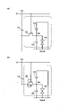
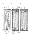
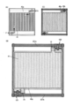
図1(A)に、透過型の液晶表示装置の断面図を示す。図1(A)に示す液晶表示装置は、基板31、トランジスタ102、絶縁層215、導電層46、絶縁層44、画素電極41、絶縁層45、共通電極43、液晶層42、及び基板32を有する。<Configuration Example 1 of Display Device>
FIG. 1A shows a cross-sectional view of a transmissive liquid crystal display device. The liquid crystal display device shown in FIG. have.
トランジスタ102は、基板31上に位置する。絶縁層215はトランジスタ102上に位置する。導電層46は、絶縁層215上に位置する。絶縁層44は、トランジスタ102、絶縁層215、及び導電層46上に位置する。画素電極41は、絶縁層44上に位置する。絶縁層45は、画素電極41上に位置する。共通電極43は、絶縁層45上に位置する。液晶層42は、共通電極43上に位置する。共通電極43は、画素電極41を介して、導電層46と重なる領域を有する。画素電極41はトランジスタ102のソースまたはドレインと電気的に接続される。導電層46、画素電極41、及び共通電極43は、それぞれ、可視光を透過する機能を有する。
本実施の形態の液晶表示装置は、画素電極41と共通電極43とが絶縁層45を介して積層され、FFS(Fringe Field Switching)モードで動作する。画素電極41、液晶層42、及び共通電極43は、液晶素子106として機能することができる。The liquid crystal display device of the present embodiment has a
導電層46、絶縁層44、及び画素電極41は、1つの容量素子104として機能することができる。また、画素電極41、絶縁層45、及び共通電極43は、1つの容量素子105として機能することができる。このように、本実施の形態の液晶表示装置は、画素に2つの容量素子を有する。したがって、画素の保持容量を大きくすることができる。The
また、2つの容量素子はいずれも可視光を透過する材料で形成され、かつ、互いに重なる領域を有する。これにより、画素は、高い開口率と、大きな保持容量と、を両立することができる。Both of the two capacitive elements are made of a material that transmits visible light, and have regions that overlap each other. Accordingly, the pixel can achieve both a high aperture ratio and a large storage capacitance.
透過型の液晶表示装置の開口率(画素の開口率ともいえる)を高めることで、液晶表示装置の高精細化が可能となる。また、開口率を高めることで、光取り出し効率(または画素の透過率)を高めることができる。これにより、液晶表示装置の消費電力を低減させることができる。By increasing the aperture ratio (which can also be called the aperture ratio of pixels) of a transmissive liquid crystal display device, it is possible to increase the definition of the liquid crystal display device. In addition, by increasing the aperture ratio, the light extraction efficiency (or pixel transmittance) can be increased. Thereby, the power consumption of the liquid crystal display device can be reduced.
画素の保持容量を大きくすることで、液晶素子等のリーク電流が大きくても安定した表示を行うことができる。また、容量の大きい液晶材料を駆動させることができる。そのため、液晶材料の選択の幅を広げることができる。By increasing the storage capacity of the pixel, stable display can be performed even if the leak current of the liquid crystal element or the like is large. In addition, it is possible to drive a liquid crystal material having a large capacity. Therefore, the range of selection of liquid crystal materials can be expanded.
画素の保持容量を大きくすることで、画素の階調を長時間にわたって保持することができる。具体的には、画素の保持容量を大きくすることで、1フレーム期間ごとに画像信号の書き換えを行わずに前の期間に書きこんだ画像信号を保持させることができ、例えば数フレームまたは数10フレームの期間にわたって画素の階調を保持することが可能となる。By increasing the storage capacitance of the pixel, the gradation of the pixel can be retained for a long time. Specifically, by increasing the storage capacitance of the pixel, the image signal written in the previous period can be retained without rewriting the image signal every frame period. It is possible to retain the grayscale of the pixels over the period of the frame.
容量素子104の容量は、容量素子105の容量よりも大きいことが好ましい。例えば、画素電極41と導電層46とが重なる領域の面積は、画素電極41と共通電極43とが重なる領域の面積より大きいことが好ましい。また、導電層46と画素電極41との間に位置する絶縁層44の厚さT1は、画素電極41と共通電極43との間に位置する絶縁層45の厚さT2よりも薄いことが好ましい。The capacitance of the
本実施の形態の表示装置の構成は、タッチパネルに適用することもできる。図1(B)は、図1(A)に示す表示装置にタッチセンサTCを搭載した例である。タッチセンサTCを表示装置の表示面に近い位置に設けることで、タッチセンサTCの感度を高めることができる。The structure of the display device of this embodiment can also be applied to a touch panel. FIG. 1B shows an example in which the display device shown in FIG. 1A is equipped with a touch sensor TC. By providing the touch sensor TC at a position close to the display surface of the display device, the sensitivity of the touch sensor TC can be enhanced.
本発明の一態様のタッチパネルが有する検知素子(センサ素子ともいう)に限定は無い。指やスタイラスなどの被検知体の近接または接触を検知することのできる様々なセンサを、検知素子として適用することができる。There is no limitation on the sensing element (also referred to as a sensor element) included in the touch panel of one embodiment of the present invention. Various sensors capable of detecting the proximity or contact of an object to be detected such as a finger or a stylus can be applied as sensing elements.
センサの方式としては、例えば、静電容量方式、抵抗膜方式、表面弾性波方式、赤外線方式、光学方式、感圧方式など様々な方式を用いることができる。As the sensor system, various systems such as an electrostatic capacity system, a resistive film system, a surface acoustic wave system, an infrared system, an optical system, and a pressure-sensitive system can be used.
静電容量方式としては、表面型静電容量方式、投影型静電容量方式等がある。また、投影型静電容量方式としては、自己容量方式、相互容量方式等がある。相互容量方式を用いると、同時多点検知が可能となるため好ましい。The capacitance method includes a surface capacitance method, a projected capacitance method, and the like. Also, the projective capacitance method includes a self-capacitance method, a mutual capacitance method, and the like. It is preferable to use the mutual capacitance method because it enables simultaneous multi-point detection.
本発明の一態様のタッチパネルは、別々に作製された表示装置と検知素子とを貼り合わせる構成、表示素子を支持する基板及び対向基板の一方または双方に検知素子を構成する電極等を設ける構成等、様々な構成を適用することができる。A touch panel of one embodiment of the present invention includes a structure in which a display device and a detection element that are separately manufactured are attached to each other, a structure in which an electrode or the like that constitutes a detection element is provided on one or both of a substrate that supports a display element and a counter substrate, and the like. , various configurations can be applied.
<表示装置の構成例2>
図2~図7を用いて、画素に、1つのトランジスタと、2つの容量素子と、を有する表示装置の構成例について説明する。<Configuration Example 2 of Display Device>
Structural examples of a display device in which a pixel includes one transistor and two capacitors are described with reference to FIGS.
≪回路≫
図2(A)、(B)に、画素11aの回路図を示す。≪Circuit≫
2A and 2B show circuit diagrams of the
図2(A)、(B)に示す画素11aは、トランジスタ102、容量素子104、容量素子105、及び液晶素子106を有する。また、画素11aには、配線121及び配線124が接続されている。A
図2(A)では、トランジスタ102がバックゲートを有さない例を示し、図2(B)では、トランジスタ102がバックゲートを有する例を示す。図2(B)では、バックゲートが、ゲートと電気的に接続されている例を示すが、バックゲートの接続はこれに限定されない。FIG. 2A shows an example in which the
トランジスタ102のソースまたはドレインの一方は、容量素子104の一方の電極、容量素子105の一方の電極、及び液晶素子106の一方の電極と電気的に接続される。One of the source and drain of the
ここで、トランジスタ102のソースまたはドレインの一方、容量素子104の一方の電極、容量素子105の一方の電極、及び液晶素子106の一方の電極が接続されるノードをノードNAとする。Here, a node NA is a node to which one of the source and the drain of the
トランジスタ102のゲートは、配線121と電気的に接続される。トランジスタ102のソースまたはドレインの他方は、配線124と電気的に接続される。容量素子104の他方の電極、容量素子105の他方の電極、及び液晶素子106の他方の電極は、それぞれ、共通配線VCOMと電気的に接続される。共通配線VCOMには任意の電位を供給することができる。A gate of the
配線121は走査線と呼ぶことができ、トランジスタの動作を制御する機能を有する。配線124は、画像信号を供給する信号線としての機能を有する。The
トランジスタ102に極めてオフ電流の低いトランジスタを用いることで、ノードNAの電位を長時間保持することができる。当該トランジスタには、例えば、金属酸化物をチャネル形成領域に用いたトランジスタ(以下、OSトランジスタ)を用いることができる。By using a transistor with extremely low off-state current as the
または、画素が有するトランジスタにシリコンをチャネル形成領域に有するトランジスタ(以下、Siトランジスタ)を適用してもよい。Siトランジスタとしては、アモルファスシリコンを有するトランジスタ、結晶性のシリコン(代表的には、低温ポリシリコンや、単結晶シリコン)を有するトランジスタなどが挙げられる。Alternatively, a transistor including silicon in a channel formation region (hereinafter referred to as a Si transistor) may be used as the transistor included in the pixel. Examples of Si transistors include transistors containing amorphous silicon, transistors containing crystalline silicon (typically low-temperature polysilicon and single-crystal silicon), and the like.
例えば、1フレーム期間ごとに画像信号を書き換える場合、OSトランジスタを用いてもよく、Siトランジスタを用いてもよい。ノードNAの電位を長時間保持する必要がある場合、SiトランジスタよりもOSトランジスタを用いることが好ましい。For example, when an image signal is rewritten every frame period, an OS transistor or a Si transistor may be used. When the potential of the node NA needs to be held for a long time, it is preferable to use an OS transistor rather than a Si transistor.
≪表示モジュールの上面レイアウト≫
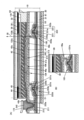
図3に、表示モジュールの上面図を示す。<<Top layout of display module>>
FIG. 3 shows a top view of the display module.
図3に示す表示モジュールは、表示装置と、表示装置に接続された集積回路(IC)及びフレキシブルプリント回路基板(FPCa、FPCb)と、を有する。The display module shown in FIG. 3 includes a display device, an integrated circuit (IC) and flexible printed circuit boards (FPCa, FPCb) connected to the display device.
表示装置は、表示領域100、ゲートドライバGD_L、及びゲートドライバGD_Rを有する。The display device has a
表示領域100は、複数の画素11を有し、画像を表示する機能を有する。The
画素11は、副画素と呼ぶこともできる。例えば、赤色を呈する副画素、緑色を呈する副画素、及び青色を呈する副画素によって1つの画素ユニットが構成されることで、表示領域100ではフルカラーの表示を行うことができる。なお、副画素が呈する色は、赤、緑、及び青に限られない。画素ユニットには、例えば、白、黄、マゼンタ、またはシアン等の色を呈する副画素を用いてもよい。なお、本明細書等において、副画素を単に画素と記す場合がある。
表示装置は、走査線駆動回路(ゲートドライバ)、信号線駆動回路(ソースドライバ)、及びタッチセンサ用の駆動回路のうち一つまたは複数を内蔵していてもよい。また、これらのうち一つまたは複数が外付けされていてもよい。図3に示す表示装置は、ゲートドライバを内蔵しており、ソースドライバを有するICが外付けされている。The display device may incorporate one or more of a scanning line driving circuit (gate driver), a signal line driving circuit (source driver), and a touch sensor driving circuit. Also, one or more of these may be externally attached. The display device shown in FIG. 3 incorporates a gate driver and externally attaches an IC having a source driver.
ゲートドライバGD_L及びゲートドライバGD_Rのうち、一方は奇数行の画素を制御する機能を有し、他方は偶数行の画素を制御する機能を有する。例えば、m行目の画素は走査線GL_mと接続され、ゲートドライバGD_Lによって制御される。また、m+1行目の画素は走査線GL_m+1と接続され、ゲートドライバGD_Rによって制御される。n列目の信号線SL_nには、ゲートドライバGD_Lと電気的に接続される画素11と、ゲートドライバGD_Rと電気的に接続される画素11と、が交互に接続される。ゲートドライバを互いに対向する二辺に分けて設けることで、1つのゲートドライバに接続される配線のピッチを広くすることができる。また、ゲートドライバを一辺にのみ設ける場合、当該辺側の非表示領域が広くなってしまう。このことから、ゲートドライバを二辺に分けて設けることで、表示装置の各辺の非表示領域を狭くし、狭額縁化できる。One of the gate driver GD_L and the gate driver GD_R has a function of controlling odd-numbered pixels, and the other has a function of controlling even-numbered pixels. For example, the pixels in the m-th row are connected to the scanning line GL_m and controlled by the gate driver GD_L. Also, the m+1-th row pixels are connected to the scanning line GL_m+1 and controlled by the gate driver GD_R.
ゲートドライバGD_L及びゲートドライバGD_Rには、FPCaを介して外部から信号及び電力が供給される。ICには、FPCbを介して外部から信号及び電力が供給される。A signal and power are supplied from the outside through the FPCa to the gate driver GD_L and the gate driver GD_R. Signals and power are supplied to the IC from the outside through the FPCb.
≪画素の上面レイアウト≫
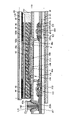
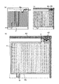
図4(A)~(C)に、画素の上面図を示す。図4(A)は、ゲート221から共通電極43aまでの積層構造を共通電極43a側から見た上面図である。図4(B)は、図4(A)の積層構造から共通電極43aを除いた上面図であり、図4(C)は、図4(A)の積層構造から共通電極43a及び画素電極41を除いた上面図である。≪Pixel Top Layout≫
4A to 4C show top views of pixels. FIG. 4A is a top view of the laminated structure from the
画素は、接続部71と接続部72を有する。接続部71では、画素電極41がトランジスタ102と電気的に接続されている。具体的には、トランジスタ102のソースまたはドレインとして機能する導電層222aが導電層46bと接し、導電層46bが画素電極41と接している。なお、導電層46bは設けなくてもよく、導電層222aが画素電極41と接していてもよい。接続部72では、導電層46aが共通電極43aと電気的に接続されている。具体的には、導電層46aが共通電極43aと接している。The pixel has a
共通電極43aは1つまたは複数のスリットを有してもよく、また櫛歯状の上面形状を有していてもよい。図4(A)に示す共通電極43aは、複数のスリットが設けられた上面形状を有する。画素電極41は、共通電極43aと重なる領域と、共通電極43aと重ならない領域と、の双方を有する。これら2つの領域はどちらも、着色層39(図5参照)と重なる位置に設けられる。The
また、画素電極41は1つまたは複数のスリットを有してもよく、また櫛歯状の上面形状を有していてもよい。共通電極43aと重なる面積を広くできるため、画素電極41を広い面積で形成することが好ましい。そのため、画素電極41はスリットを有さない島状に形成されることが好ましい。Further, the
≪表示モジュールの断面構造≫
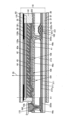
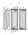
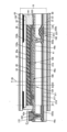
図5に、表示モジュールの断面図を示す。なお、画素の断面構造については、図4(A)に示す一点鎖線A1-A2間の断面図に相当する。≪Cross-sectional structure of the display module≫
FIG. 5 shows a cross-sectional view of the display module. Note that the cross-sectional structure of the pixel corresponds to the cross-sectional view taken along the dashed-dotted line A1-A2 in FIG. 4A.
図5に示す表示モジュールは、表示装置10、偏光板61、偏光板63、バックライトユニット30、FPC172等を有する。The display module shown in FIG. 5 has a
バックライトユニット30が有する光源から発せられた光35は、偏光板61、表示装置10、偏光板63をこの順に透過して、表示モジュールの外部に射出される。光35が透過するこれらの層の材料には、可視光を透過する材料を用いる。
表示装置10は着色層39を有するため、カラー画像を表示することができる。バックライトユニット30が有する光源から発せられた光35は、着色層39によって特定の波長領域以外の光が吸収される。これにより、例えば、赤色の画素(副画素)から表示モジュールの外部に射出される光は赤色を呈し、緑色の副画素(副画素)から表示モジュールの外部に射出される光は緑色を呈し、青色の副画素(副画素)から表示モジュールの外部に射出される光は青色を呈する。Since the
表示装置10は、FFSモードが適用されたアクティブマトリクス型の液晶表示装置である。表示装置10は、透過型の液晶表示装置である。The
表示装置10は、基板31、基板32、トランジスタ102、導電層46a、導電層46b、導電層46c、絶縁層44、絶縁層45、画素電極41、液晶層42、共通電極43a、導電層43b、導電層222e、配向膜133a、配向膜133b、接着層141、オーバーコート135、遮光層38、及び着色層39等を有する。The
基板31上にトランジスタ102が位置する。トランジスタ102は、ゲート221、ゲート絶縁層211、半導体層231、導電層222a、導電層222b、絶縁層217、絶縁層218、絶縁層215、及びゲート223を有する。導電層222a及び導電層222bのうち一方はソースとして機能し、他方はドレインとして機能する。絶縁層217、絶縁層218、及び絶縁層215はゲート絶縁層として機能する。
ここでは、半導体層231に金属酸化物を用いる場合を例に挙げて説明する。Here, the case where a metal oxide is used for the
半導体層231と接するゲート絶縁層211及び絶縁層217は酸化物絶縁層であることが好ましい。なお、ゲート絶縁層211または絶縁層217が積層構造である場合、少なくとも半導体層231と接する層が酸化物絶縁層であることが好ましい。これにより、半導体層231に酸素欠損が生じることを抑制でき、トランジスタの信頼性を高めることができる。The
絶縁層218は窒化物絶縁層であることが好ましい。これにより、半導体層231に不純物が入り込むことを抑制でき、トランジスタの信頼性を高めることができる。Insulating
絶縁層215は、平坦化機能を有することが好ましく、例えば、有機絶縁層であることが好ましい。なお、絶縁層215は形成しなくてもよく、絶縁層218上に接して導電層46aを形成してもよい。The insulating
絶縁層215上に導電層46bが位置し、導電層46b上に絶縁層44が位置し、絶縁層44上に画素電極41が位置する。画素電極41は、導電層222aと電気的に接続されている。具体的には、導電層222aは導電層46bと接し、導電層46bは画素電極41と接している。A
絶縁層215上に導電層46aが位置する。導電層46a上に絶縁層44及び絶縁層45が位置する。絶縁層45上に共通電極43aが位置する。共通電極43aは、導電層46aと電気的に接続されている。具体的には、共通電極43aは、絶縁層44及び絶縁層45に設けられた開口を介して、導電層46aと接している。
基板32には、遮光層38及び着色層39が設けられ、そして、遮光層38及び着色層39を覆うオーバーコート135が設けられている。オーバーコート135に接して配向膜133bが設けられている。また、共通電極43a上に配向膜133aが設けられている。配向膜133aと配向膜133bの間に液晶層42が挟持されている。オーバーコート135は、着色層39及び遮光層38等に含まれる不純物が液晶層42に拡散することを抑制できる。The
基板31と基板32は接着層141によって貼り合わされている。The
FPC172は、導電層222eと電気的に接続されている。具体的には、FPC172は接続体242と接し、接続体242は導電層43bと接し、導電層43bは導電層46cと接し、導電層46cは導電層222eと接する。導電層43bは絶縁層45上に形成され、導電層46cは絶縁層215上に形成され、導電層222eは、ゲート絶縁層211上に形成されている。導電層43bは、共通電極43aと同一の工程、同一の材料で形成することができる。導電層46cは、ゲート223、導電層46a、導電層46bと同一の工程、同一の材料で形成することができる。導電層222eは、導電層222a及び導電層222bと同一の工程、同一の材料で形成することができる。The
導電層46a、絶縁層44、及び画素電極41は、1つの容量素子104として機能することができる。また、画素電極41、絶縁層45、及び共通電極43aは、1つの容量素子105として機能することができる。このように、表示装置10は、1つの画素に2つの容量素子を有する。したがって、画素の保持容量を大きくすることができる。The
また、2つの容量素子はいずれも可視光を透過する材料で形成され、かつ、互いに重なる領域を有する。これにより、画素は、高い開口率と、大きな保持容量と、を両立することができる。Both of the two capacitive elements are made of a material that transmits visible light, and have regions that overlap each other. Accordingly, the pixel can achieve both a high aperture ratio and a large storage capacitance.
容量素子104の容量は、容量素子105の容量よりも大きいことが好ましい。そのため、画素電極41と導電層46aとが重なる領域の面積は、画素電極41と共通電極43aとが重なる領域の面積より大きいことが好ましい。また、導電層46aと画素電極41との間に位置する絶縁層44の厚さは、画素電極41と共通電極43aとの間に位置する絶縁層45の厚さよりも薄いことが好ましい。The capacitance of the
図5では、トランジスタ102がバックゲート(図5ではゲート223)を有する例を示したが、図6に示すように、トランジスタ102はバックゲートを有していなくてもよい。図6に示すトランジスタ102は、ゲート221、ゲート絶縁層211、半導体層231、導電層222a、及び導電層222bを有する。図6に示すトランジスタ102は、絶縁層217、絶縁層218、及び絶縁層215に覆われている。Although FIG. 5 shows an example in which the
図7に示す表示装置10は、トランジスタ102の構造が図5及び図6とは異なる。The
図7に示すトランジスタ102は、ゲート221、ゲート絶縁層211、半導体層231、導電層222a、導電層222b、絶縁層212、絶縁層213、ゲート絶縁層225、及びゲート223を有する。導電層222a及び導電層222bのうち一方はソースとして機能し、他方はドレインとして機能する。トランジスタ102は、絶縁層214及び絶縁層215に覆われている。A
図7に示すトランジスタ102は、チャネルの上下にゲートを有する。2つのゲートは、電気的に接続されていることが好ましい。2つのゲートが電気的に接続されている構成のトランジスタは、他のトランジスタと比較して電界効果移動度を高めることが可能であり、オン電流を増大させることができる。その結果、高速動作が可能な回路を作製することができる。さらには回路部の占有面積を縮小することが可能となる。オン電流の大きなトランジスタを適用することで、表示装置を大型化、または高精細化して配線数が増大したとしても、各配線における信号遅延を低減することが可能であり、表示ムラを抑制することが可能である。また、回路部の占有面積を縮小できるため、表示装置の狭額縁化が可能である。また、このような構成を適用することで、信頼性の高いトランジスタを実現することができる。The
半導体層231は、一対の低抵抗領域231nと、一対の低抵抗領域231nの間に挟持されたチャネル形成領域231iと、を有する。The
チャネル形成領域231iは、ゲート絶縁層211を介してゲート221と重なり、ゲート絶縁層225を介してゲート223と重なる。The
ここでは、半導体層231に金属酸化物を用いる場合を例に挙げて説明する。Here, the case where a metal oxide is used for the
チャネル形成領域231iと接するゲート絶縁層211及びゲート絶縁層225は酸化物絶縁層であることが好ましい。なお、ゲート絶縁層211またはゲート絶縁層225が積層構造である場合、少なくともチャネル形成領域231iと接する層が酸化物絶縁層であることが好ましい。これにより、チャネル形成領域231iに酸素欠損が生じることを抑制でき、トランジスタの信頼性を高めることができる。The
絶縁層213及び絶縁層214のうち一方または双方は窒化物絶縁層であることが好ましい。これにより、半導体層231に不純物が入り込むことを抑制でき、トランジスタの信頼性を高めることができる。One or both of insulating
絶縁層215は、平坦化機能を有することが好ましく、例えば、有機絶縁層であることが好ましい。なお、絶縁層214及び絶縁層215のうち一方または双方は形成しなくてもよい。The insulating
低抵抗領域231nは、チャネル形成領域231iよりも抵抗率が低い。低抵抗領域231nは半導体層231のうち絶縁層212と接する領域である。ここで、絶縁層212が窒素または水素を有することが好ましい。これにより、絶縁層212中の窒素または水素が低抵抗領域231nに入り込み、低抵抗領域231nのキャリア濃度を高めることができる。または、ゲート223をマスクとして、不純物を添加することで、低抵抗領域231nを形成してもよい。当該不純物としては、例えば、水素、ヘリウム、ネオン、アルゴン、フッ素、窒素、リン、ヒ素、アンチモン、ホウ素、アルミニウム、マグネシウム、シリコンなどが挙げられ、当該不純物は、イオン注入法またはイオンドーピング法を用いて添加することができる。また、上記不純物以外にも、半導体層231の構成元素の一つである、インジウムなどを添加することで低抵抗領域231nを形成してもよい。インジウムを添加することで、チャネル形成領域231iよりも低抵抗領域231nの方が、インジウムの濃度が高くなる場合がある。The
また、ゲート絶縁層235及びゲート233を形成した後に、半導体層231の一部の領域に接するように第1の層を形成し、加熱処理を施すことにより、当該領域を低抵抗化させ、低抵抗領域231nを形成することができる。Further, after the gate insulating layer 235 and the gate 233 are formed, a first layer is formed so as to be in contact with part of a region of the
第1の層としては、アルミニウム、チタン、タンタル、タングステン、クロム、及びルテニウムなどの金属元素の少なくとも一を含む膜を用いることができる。特に、アルミニウム、チタン、タンタル、及びタングステンの少なくとも一を含むことが好ましい。または、これら金属元素の少なくとも一を含む窒化物、またはこれら金属元素の少なくとも一を含む酸化物を好適に用いることができる。特に、タングステン膜、チタン膜などの金属膜、窒化アルミニウムチタン膜、窒化チタン膜、窒化アルミニウム膜などの窒化物膜、酸化アルミニウムチタン膜などの酸化物膜などを好適に用いることができる。As the first layer, a film containing at least one of metal elements such as aluminum, titanium, tantalum, tungsten, chromium, and ruthenium can be used. In particular, it preferably contains at least one of aluminum, titanium, tantalum, and tungsten. Alternatively, a nitride containing at least one of these metal elements or an oxide containing at least one of these metal elements can be preferably used. In particular, a metal film such as a tungsten film or a titanium film, a nitride film such as an aluminum titanium nitride film, a titanium nitride film, or an aluminum nitride film, an oxide film such as an aluminum titanium oxide film, or the like can be preferably used.
第1の層の厚さは、例えば0.5nm以上20nm以下、好ましくは0.5nm以上15nm以下、より好ましくは0.5nm以上10nm以下、さらに好ましくは1nm以上6nm以下とすることができる。代表的には、5nm程度、または約2nm程度とすることができる。第1の層がこのように薄い場合であっても、十分に半導体層231を低抵抗化できる。The thickness of the first layer can be, for example, 0.5 nm or more and 20 nm or less, preferably 0.5 nm or more and 15 nm or less, more preferably 0.5 nm or more and 10 nm or less, still more preferably 1 nm or more and 6 nm or less. Typically, it can be about 5 nm, or about 2 nm. Even when the first layer is thin like this, the resistance of the
低抵抗領域231nは、チャネル形成領域231iよりもキャリア密度の高い領域とすることが重要である。例えば低抵抗領域231nは、チャネル形成領域231iよりも水素を多く含む領域、または、チャネル形成領域231iよりも酸素欠損を多く含む領域とすることができる。酸化物半導体中の酸素欠損と水素原子とが結合すると、キャリアの発生源となる。It is important that the
半導体層231の一部の領域に第1の層を接して設けた状態で、加熱処理を行うことで、当該領域中の酸素が第1の層に吸引され、当該領域中に酸素欠損を多く形成することができる。これにより、低抵抗領域231nを極めて低抵抗な領域とすることができる。Heat treatment is performed in a state where the first layer is in contact with part of a region of the
このように形成された低抵抗領域231nは、後の処理で高抵抗化しにくいといった特徴を有する。例えば、酸素を含む雰囲気下での加熱処理や、酸素を含む雰囲気下での成膜処理などを行っても、低抵抗領域231nの導電性が損なわれる恐れがないため、電気特性が良好で、且つ信頼性の高いトランジスタを実現できる。The low-
加熱処理を経た後の第1の層が導電性を有する場合には、加熱処理後に第1の層を除去することが好ましい。一方、第1の層が絶縁性を有する場合には、これを残存させることで第1の層を保護絶縁膜として機能させることができる。When the first layer after heat treatment has conductivity, it is preferable to remove the first layer after the heat treatment. On the other hand, when the first layer has an insulating property, the first layer can function as a protective insulating film by leaving the insulating property.
FPC172は、導電層222eと電気的に接続されている。具体的には、FPC172は接続体242と接し、接続体242は導電層43bと接し、導電層43bは導電層222eと接する。導電層43bは絶縁層45上に形成され、導電層222eは、絶縁層214上に形成されている。導電層43bは、共通電極43aと同一の工程、同一の材料で形成することができる。導電層222eは、導電層222a及び導電層222bと同一の工程、同一の材料で形成することができる。The
<表示装置の構成例3>
図8~図12を用いて、画素に、2つのトランジスタと、2つの容量素子と、を有する表示装置の構成例について説明する。<Configuration Example 3 of Display Device>
Structural examples of a display device in which a pixel includes two transistors and two capacitors are described with reference to FIGS.
本発明の一態様の表示装置は、画像信号に補正信号を付加するための機能を有する。A display device of one embodiment of the present invention has a function of adding a correction signal to an image signal.
当該補正信号は、容量結合によって画像信号に付加され、液晶素子に供給される。したがって、液晶素子では補正された画像を表示することができる。当該補正によって、例えば、液晶素子は、画像信号のみを用いて表現できる階調よりも多くの階調を表現することができる。The correction signal is added to the image signal by capacitive coupling and supplied to the liquid crystal element. Therefore, the liquid crystal element can display a corrected image. By this correction, for example, the liquid crystal element can express more gradations than can be expressed using only the image signal.
また、当該補正によって、ソースドライバの出力電圧よりも高い電圧で、液晶素子を駆動させることができる。画素内で、液晶素子に供給する電圧を所望の値に変えることができるため、既存のソースドライバを転用でき、ソースドライバを新規に設計するコストなどを削減することができる。また、ソースドライバの出力電圧が高くなることを抑制でき、ソースドライバの消費電力を低減することができる。Further, the correction can drive the liquid crystal element with a voltage higher than the output voltage of the source driver. Since the voltage supplied to the liquid crystal element can be changed to a desired value within the pixel, an existing source driver can be used, and the cost of designing a new source driver can be reduced. In addition, it is possible to prevent the output voltage of the source driver from increasing and to reduce the power consumption of the source driver.
高い電圧をかけて液晶素子を駆動させることで、表示装置を広い温度範囲で使用することができ、低温環境及び高温環境のいずれにおいても信頼性高く表示を行うことができる。例えば、当該表示装置を車載用またはカメラ用の表示装置として利用することができる。By applying a high voltage to drive the liquid crystal element, the display device can be used in a wide temperature range, and display can be performed with high reliability both in a low-temperature environment and a high-temperature environment. For example, the display device can be used as an in-vehicle display device or a camera display device.
また、高い電圧をかけて液晶素子を駆動させることができるため、ブルー相を示す液晶など、駆動電圧の高い液晶材料を用いることもでき、液晶材料の選択の幅を広げることができる。In addition, since the liquid crystal element can be driven by applying a high voltage, a liquid crystal material with a high driving voltage such as a liquid crystal exhibiting a blue phase can be used, and the range of selection of the liquid crystal material can be widened.
また、高い電圧をかけて液晶素子を駆動させることができるため、液晶素子に印加する電圧を一時的に高くして液晶の配向を速く変化させるオーバードライブ駆動により液晶の応答速度を向上させることもできる。In addition, since the liquid crystal element can be driven by applying a high voltage, it is also possible to improve the response speed of the liquid crystal by overdrive driving that temporarily increases the voltage applied to the liquid crystal element and changes the orientation of the liquid crystal quickly. can.
また、高い電圧をかけて液晶素子を駆動させることで、表示の焼き付きを低減できる。In addition, display burn-in can be reduced by applying a high voltage to drive the liquid crystal element.
補正信号は、例えば、外部機器にて生成され、各画素に書き込まれる。補正信号の生成は、外部機器を用いてリアルタイムで行ってもよいし、記録媒体に保存されている補正信号を読み出して画像信号と同期させてもよい。The correction signal is generated, for example, by an external device and written to each pixel. The correction signal may be generated in real time using an external device, or the correction signal stored in the recording medium may be read out and synchronized with the image signal.
本発明の一態様の表示装置では、供給する画像信号は変化させず、補正信号を供給した画素で新たな画像信号を生成することができる。外部機器を用いて新しい画像信号そのものを生成する場合に比べて、外部機器にかかる負荷を低減することができる。また、新たな画像信号を画素で生成するための動作は少ないステップで行うことができ、画素数が多く水平期間の短い表示装置でも対応することができる。In the display device of one embodiment of the present invention, a new image signal can be generated by the pixel to which the correction signal is supplied without changing the supplied image signal. The load on the external device can be reduced compared to the case where the new image signal itself is generated using the external device. In addition, the operation for generating a new image signal with pixels can be performed in a small number of steps, and a display device with a large number of pixels and a short horizontal period can also be used.
≪回路≫
図8(A)に、画素11bの回路図を示す。≪Circuit≫
FIG. 8A shows a circuit diagram of the
画素11bは、トランジスタ101、トランジスタ102、容量素子104、容量素子105、及び液晶素子106を有する。The
トランジスタ101のソースまたはドレインの一方は、容量素子104の一方の電極と電気的に接続される。容量素子104の他方の電極は、トランジスタ102のソースまたはドレインの一方、容量素子105の一方の電極、及び液晶素子106の一方の電極と電気的に接続される。One of the source and drain of the
ここで、トランジスタ101のソースまたはドレインの一方及び容量素子104の一方の電極が接続されるノードをノードNSとする。容量素子104の他方の電極、トランジスタ102のソースまたはドレインの一方、容量素子105の一方の電極、及び液晶素子106の一方の電極が接続されるノードをノードNAとする。Here, a node to which one of the source and drain of the
トランジスタ101のゲートは、配線122と電気的に接続される。トランジスタ102のゲートは、配線121と電気的に接続される。トランジスタ101のソースまたはドレインの他方は、配線125と電気的に接続される。トランジスタ102のソースまたはドレインの他方は、配線124と電気的に接続される。A gate of the
容量素子105の他方の電極及び液晶素子106の他方の電極は、それぞれ、共通配線VCOMと電気的に接続される。共通配線VCOMには任意の電位を供給することができる。The other electrode of the
配線121及び配線122はそれぞれ走査線と呼ぶことができ、トランジスタの動作を制御する機能を有する。配線125は、画像信号を供給する信号線としての機能を有する。配線124は、ノードNAにデータを書き込むための信号線としての機能を有する。Each of the
図8(A)に示す各トランジスタは、ゲートと電気的に接続されたバックゲートを有するが、バックゲートの接続はこれに限定されない。また、トランジスタにバックゲートを設けなくてもよい。Each transistor illustrated in FIG. 8A has a back gate electrically connected to the gate, but the connection of the back gate is not limited to this. In addition, the transistor need not have a back gate.
トランジスタ101を非導通とすることで、ノードNSの電位を保持することができる。また、トランジスタ102を非導通とすることで、ノードNAの電位を保持することができる。また、トランジスタ102を非導通とした状態で、トランジスタ101を介してノードNSに所定の電位を供給することで、容量素子104を介した容量結合により、ノードNSの電位の変化に応じてノードNAの電位を変化させることができる。By turning off the
画素11bにおいて、配線124からノードNAに書き込まれた補正信号は、配線125から供給される画像信号と容量結合され、液晶素子106に供給される。したがって、液晶素子106では補正された画像を表示することができる。In the
トランジスタ101に極めてオフ電流の低いトランジスタを用いることで、ノードNSの電位を長時間保持することができる。同様に、トランジスタ102に極めてオフ電流の低いトランジスタを用いることで、ノードNAの電位を長時間保持することができる。極めてオフ電流の低いトランジスタとして、例えば、OSトランジスタが挙げられる。また、画素が有するトランジスタにSiトランジスタを適用してもよい。または、OSトランジスタと、Siトランジスタとの両方を用いてもよい。By using a transistor with extremely low off-state current as the
例えば、1フレーム期間ごとに補正信号及び画像信号を書き換える場合、トランジスタ101及びトランジスタ102には、OSトランジスタを用いてもよく、Siトランジスタを用いてもよい。ノードNSまたはノードNAの電位を長時間保持する必要がある場合、トランジスタ101及びトランジスタ102には、SiトランジスタよりもOSトランジスタを用いることが好ましい。For example, when the correction signal and the image signal are rewritten every frame period, the
≪タイミングチャート≫
図8(B)に示すタイミングチャートを用いて、画素11bにおける補正信号(Vp)をノードNMに書き込む動作を説明する。画像信号(Vs)の補正を目的とする場合、補正信号Vpの書き込みは、フレーム毎に行うことが好ましい。なお、配線124に供給される補正信号(Vp)には正負の任意の信号を用いることができるが、ここでは正の信号が供給される場合を説明する。また、以下の説明においては、高電位を“H”、低電位を“L”で表す。≪Timing chart≫
The operation of writing the correction signal (Vp) in the
時刻T1に配線121の電位を“H”、配線122の電位を“L”、配線124の電位を“L”、配線125の電位を“L”とすると、トランジスタ102が導通し、ノードNAの電位は配線124の電位となる。このとき、配線124の電位をリセット電位(例えば“L”)とすることで、液晶素子106の動作をリセットすることができる。When the potential of the
なお、時刻T1より前は、前フレームにおける液晶素子106の表示動作が行われている状態である。Before time T1, the display operation of the
時刻T2に配線121の電位を“L”、配線122の電位を“H”、配線124の電位を“Vp”、配線125の電位を“L”とすると、トランジスタ101が導通し、容量素子104の他方の電極の電位は“L”となる。当該動作は、後の容量結合動作を行うためのリセット動作である。When the potential of the
時刻T3に配線121の電位を“H”、配線122の電位を“H”、配線124の電位を“Vp”、配線125の電位を“L”とすると、ノードNAに配線124の電位(補正信号(Vp))が書き込まれる。Assuming that the potential of the
時刻T4に配線121の電位を“L”、配線122の電位を“H”、配線124の電位を“Vp”、配線125の電位を“L”とすると、トランジスタ102が非導通となり、ノードNAに補正信号(Vp)が保持される。At time T4, when the potential of the
時刻T5に配線121の電位を“L”、配線122の電位を“L”、配線125の電位を“L”、配線126の電位を“L”とすると、トランジスタ101が非導通となり、補正信号(Vp)の書き込み動作が終了する。At time T5, when the potential of the
次に、図8(C)に示すタイミングチャートを用いて、画素11bにおける画像信号(Vs)の補正動作と、液晶素子106の表示動作と、を説明する。なお、配線125には、適切なタイミングで所望の電位が供給されていることとする。Next, the correction operation of the image signal (Vs) in the
時刻T11に配線121の電位を“L”、配線122の電位を“H”、配線124の電位を“L”とすると、トランジスタ101が導通し、容量素子104の容量結合によりノードNAの電位に配線125の電位が付加される。すなわち、ノードNAは、画像信号(Vs)に補正信号(Vp)が付加された電位(Vs+Vp)’となる。なお、電位(Vs+Vp)’には、配線間容量の容量結合による電位の変動なども含まれる。When the potential of the
時刻T12に配線121の電位を“L”、配線122の電位を“L”、配線124の電位を“L”とすると、トランジスタ101が非導通となり、ノードNMに電位(Vs+Vp)’が保持される。そして、当該電位に応じて液晶素子106で表示動作が行われる。At time T12, when the potential of the
以上が画像信号(Vs)の補正動作と、液晶素子106の表示動作の説明である。なお、先に説明した補正信号(Vp)の書き込み動作と、画像信号(Vs)の入力動作は連続して行ってもよく、全ての画素に補正信号(Vp)を書き込んだのちに画像信号(Vs)の入力動作を行ってもよい。The correction operation of the image signal (Vs) and the display operation of the
なお、補正動作を行わない場合は、画像信号を配線124に供給し、トランジスタ102の導通、非導通を制御することで液晶素子106による表示動作を行ってもよい。このとき、トランジスタ101は常時非導通としてもよいし、配線125に定電位を供給した状態でトランジスタ101を常時導通としてもよい。Note that when the correction operation is not performed, an image signal may be supplied to the
≪画素の上面レイアウト≫
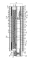
図9(A)~(C)に、画素の上面図を示す。図9(A)は、ゲート221a及びゲート221bから共通電極43aまでの積層構造を共通電極43a側から見た上面図である。図9(B)は、図9(A)の積層構造から共通電極43aを除いた上面図であり、図9(C)は、図9(A)の積層構造から共通電極43a及び画素電極41を除いた上面図である。≪Pixel Top Layout≫
9A to 9C show top views of pixels. FIG. 9A is a top view of the laminated structure from the
画素は、接続部73と接続部74を有する。接続部73では、画素電極41がトランジスタ102と電気的に接続されている。具体的には、トランジスタ102のソースまたはドレインとして機能する導電層222aが導電層46bと接し、かつ、導電層46bが画素電極41と接している。接続部74では、導電層46aがトランジスタ101と電気的に接続されている。具体的には、導電層46aがトランジスタ101のソースまたはドレインとして機能する導電層222cと接している。The pixel has a
≪表示モジュールの断面構造≫
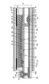
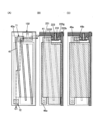
図10に、表示モジュールの断面図を示す。なお、画素の断面構造については、図9(A)に示す一点鎖線B1-B2間の断面図に相当する。≪Cross-sectional structure of the display module≫
FIG. 10 shows a cross-sectional view of the display module. Note that the cross-sectional structure of the pixel corresponds to the cross-sectional view along the dashed-dotted line B1-B2 in FIG. 9A.
図10に示す表示モジュールは、表示装置10、偏光板61、偏光板63、バックライトユニット30、FPC172等を有する。The display module shown in FIG. 10 has a
表示装置10は、基板31、基板32、トランジスタ102、導電層46a、導電層46b、絶縁層44、絶縁層45、画素電極41、液晶層42、共通電極43a、導電層43b、導電層222e、配向膜133a、配向膜133b、接着層141、オーバーコート135、遮光層38、及び着色層39等を有する。The
基板31上にトランジスタ101及びトランジスタ102が位置する。トランジスタ102は、ゲート221a、ゲート絶縁層211、半導体層231a、導電層222a、導電層222b、絶縁層212、絶縁層213、ゲート絶縁層225a、及びゲート223aを有する。トランジスタ101は、ゲート221b、ゲート絶縁層211、半導体層231b、導電層222c、導電層222d、絶縁層212、絶縁層213、ゲート絶縁層225b、及びゲート223bを有する。図10におけるトランジスタ101及びトランジスタ102の構造は、図7におけるトランジスタ102の構造と同様であるため、詳細な説明は省略する。A
絶縁層215上に導電層46bが位置し、導電層46b上に絶縁層44が位置し、絶縁層44上に画素電極41が位置する。画素電極41は、導電層222aと電気的に接続されている。具体的には、導電層222aは導電層46bと接し、導電層46bは画素電極41と接している。A
絶縁層215上に導電層46aが位置する。導電層46aは、導電層222cと電気的に接続されている。具体的には、導電層46aは、絶縁層214及び絶縁層215に設けられた開口を介して、導電層222cと接している。
基板32には、遮光層38及び着色層39が設けられ、そして、遮光層38及び着色層39を覆うオーバーコート135が設けられている。オーバーコート135に接して配向膜133bが設けられている。また、共通電極43a上に配向膜133aが設けられている。配向膜133aと配向膜133bの間に液晶層42が挟持されている。オーバーコート135は、着色層39及び遮光層38等に含まれる不純物が液晶層42に拡散することを抑制できる。The
基板31と基板32は接着層141によって貼り合わされている。The
FPC172は、導電層222eと電気的に接続されている。具体的には、FPC172は接続体242と接し、接続体242は導電層43bと接し、導電層43bは導電層222eと接する。導電層43bは絶縁層45上に形成され、導電層222eは、絶縁層214上に形成されている。導電層43bは、共通電極43aと同一の工程、同一の材料で形成することができる。導電層222eは、導電層222a~導電層222dと同一の工程、同一の材料で形成することができる。The
導電層46a、絶縁層44、及び画素電極41は、1つの容量素子104として機能することができる。また、画素電極41、絶縁層45、及び共通電極43aは、1つの容量素子105として機能することができる。このように、表示装置10は、1つの画素に2つの容量素子を有する。したがって、画素の保持容量を大きくすることができる。The
また、2つの容量素子はいずれも可視光を透過する材料で形成され、かつ、互いに重なる領域を有する。これにより、画素は、高い開口率と、大きな保持容量と、を両立することができる。Both of the two capacitive elements are made of a material that transmits visible light, and have regions that overlap each other. Accordingly, the pixel can achieve both a high aperture ratio and a large storage capacitance.
容量素子104の容量は、容量素子105の容量よりも大きいことが好ましい。そのため、画素電極41と導電層46aとが重なる領域の面積は、画素電極41と共通電極43aとが重なる領域の面積より大きいことが好ましい。また、導電層46aと画素電極41との間に位置する絶縁層44の厚さは、画素電極41と共通電極43aとの間に位置する絶縁層45の厚さよりも薄いことが好ましい。The capacitance of the
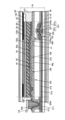
図10では、トランジスタ101及びトランジスタ102の双方がバックゲート(図10ではゲート223a、223b)を有する例を示したが、トランジスタ101及びトランジスタ102の一方または双方がバックゲートを有していなくてもよい。FIG. 10 shows an example in which both the
また、図10では、ゲート絶縁層225がチャネル形成領域231i上にのみ形成され、低抵抗領域231nと重ならない例を示したが、ゲート絶縁層225は低抵抗領域231nの少なくとも一部と重なっていてもよい。図11では、ゲート絶縁層225が低抵抗領域231n、ゲート絶縁層211と接して形成される例を示す。図11に示すゲート絶縁層225は、ゲート223をマスクに用いてゲート絶縁層225を加工する工程を削減できる、絶縁層214の被形成面の段差を低くできる等のメリットを有する。Further, FIG. 10 shows an example in which the
ゲート絶縁層225が加熱により酸素を放出する機能を有する酸化物膜である場合、加熱により低抵抗領域231nに酸素が供給され、キャリア密度の低減、電気抵抗の上昇が生じる恐れがある。そこで、ゲート絶縁層225を介して半導体層231の一部に不純物を添加することで低抵抗領域231nを形成することが好ましい。これにより、ゲート絶縁層225中にも不純物が添加される。加熱により酸素を放出する機能を有する酸化物膜に不純物を添加することで、放出される酸素の量を低減することができる。したがって、加熱によりゲート絶縁層225から低抵抗領域231nに酸素が供給されることを抑制でき、低抵抗領域231nの電気抵抗が低い状態を維持することができる。When the
図12に示す表示装置10は、トランジスタ101及びトランジスタ102の構造が図10及び図11とは異なる。The
図12に示すトランジスタ102は、ゲート221a、ゲート絶縁層211、半導体層231a、導電層222a、導電層222b、絶縁層217、絶縁層218、絶縁層215、及びゲート223aを有する。トランジスタ101は、ゲート221b、ゲート絶縁層211、半導体層231b、導電層222c、導電層222d、絶縁層217、絶縁層218、絶縁層215、及びゲート223bを有する。図12におけるトランジスタ101及びトランジスタ102の構造は、図5におけるトランジスタ102の構造と同様であるため、詳細な説明は省略する。The
≪構成要素の材料≫
次に、本実施の形態の表示装置及び表示モジュールの各構成要素に用いることができる材料等の詳細について、説明を行う。≪Materials of components≫
Next, details such as materials that can be used for each component of the display device and the display module of this embodiment are described.
表示装置が有する基板の材質などに大きな制限はなく、様々な基板を用いることができる。例えば、ガラス基板、石英基板、サファイア基板、半導体基板、セラミック基板、金属基板、またはプラスチック基板等を用いることができる。There is no particular limitation on the material of the substrate included in the display device, and various substrates can be used. For example, a glass substrate, a quartz substrate, a sapphire substrate, a semiconductor substrate, a ceramic substrate, a metal substrate, a plastic substrate, or the like can be used.
厚さの薄い基板を用いることで、表示装置の軽量化及び薄型化を図ることができる。さらに、可撓性を有する程度の厚さの基板を用いることで、可撓性を有する表示装置を実現できる。By using a thin substrate, the weight and thickness of the display device can be reduced. Furthermore, a flexible display device can be realized by using a substrate that is thick enough to be flexible.
液晶材料には、誘電率の異方性(Δε)が正であるポジ型の液晶材料と、負であるネガ型の液晶材料がある。本発明の一態様では、どちらの材料を用いることもでき、適用するモード及び設計に応じて最適な液晶材料を用いることができる。Liquid crystal materials include positive-type liquid crystal materials whose dielectric constant anisotropy (Δε) is positive and negative-type liquid crystal materials whose dielectric anisotropy (Δε) is negative. In one aspect of the present invention, either material can be used, and the most suitable liquid crystal material can be used depending on the mode and design to be applied.
本実施の形態の表示装置では、様々なモードが適用された液晶素子を用いることができる。上述したFFSモードのほかに、例えば、IPSモード、TNモード、ASM(Axially Symmetric aligned Micro-cell)モード、OCB(Optically Compensated Birefringence)モード、FLC(Ferroelectric Liquid Crystal)モード、AFLC(AntiFerroelectric Liquid Crystal)モード、ECB(Electrically Controlled Birefringence)モード、VA-IPSモード、ゲストホストモード等が適用された液晶素子を用いることができる。Liquid crystal elements to which various modes are applied can be used in the display device of this embodiment mode. In addition to the FFS mode described above, for example, IPS mode, TN mode, ASM (Axially Symmetrically aligned Micro-cell) mode, OCB (Optically Compensated Birefringence) mode, FLC (Ferroelectric Liquid Crystal) mode, AFLC (Anti-Ferroelectric Crystal) mode. , an electrically controlled birefringence (ECB) mode, a VA-IPS mode, a guest-host mode, or the like can be used.
なお、液晶素子は、液晶の光学変調作用によって光の透過または非透過を制御する素子である。液晶の光学的変調作用は、液晶にかかる電界(横方向の電界、縦方向の電界または斜め方向の電界を含む)によって制御される。液晶素子に用いる液晶としては、サーモトロピック液晶、低分子液晶、高分子液晶、高分子分散型液晶(PDLC:Polymer Dispersed Liquid Crystal)、強誘電性液晶、反強誘電性液晶等を用いることができる。これらの液晶材料は、条件により、コレステリック相、スメクチック相、キュービック相、カイラルネマチック相、等方相等を示す。Note that the liquid crystal element is an element that controls transmission or non-transmission of light by the optical modulation action of liquid crystal. The optical modulation action of liquid crystals is controlled by electric fields (including lateral, vertical, or oblique electric fields) applied to the liquid crystal. Thermotropic liquid crystals, low molecular weight liquid crystals, polymer liquid crystals, polymer dispersed liquid crystals (PDLC), ferroelectric liquid crystals, antiferroelectric liquid crystals, and the like can be used as liquid crystals used in the liquid crystal element. . These liquid crystal materials exhibit a cholesteric phase, a smectic phase, a cubic phase, a chiral nematic phase, an isotropic phase, etc., depending on conditions.
上述の通り、本実施の形態の表示装置は、高い電圧をかけて液晶素子を駆動させることができるため、ブルー相を示す液晶を用いてもよい。ブルー相は液晶相の一つであり、コレステリック液晶を昇温していくと、コレステリック相から等方相へ転移する直前に発現する相である。ブルー相は狭い温度範囲でしか発現しないため、温度範囲を改善するために5重量%以上のカイラル剤を混合させた液晶組成物を液晶層に用いる。ブルー相を示す液晶とカイラル剤とを含む液晶組成物は、応答速度が短く、光学的等方性を示す。また、ブルー相を示す液晶とカイラル剤とを含む液晶組成物は、配向処理が不要であり、視野角依存性が小さい。また配向膜を設けなくてもよいのでラビング処理も不要であり、ラビング処理によって引き起こされる静電破壊を防止することができ、作製工程中の表示パネルの不良または破損を軽減することができる。As described above, in the display device of this embodiment mode, the liquid crystal element can be driven by applying a high voltage; therefore, a liquid crystal exhibiting a blue phase may be used. The blue phase is one of the liquid crystal phases, and is a phase that appears immediately before the cholesteric phase transitions to the isotropic phase when the temperature of the cholesteric liquid crystal is increased. Since the blue phase is expressed only in a narrow temperature range, a liquid crystal composition mixed with 5% by weight or more of a chiral agent is used for the liquid crystal layer in order to improve the temperature range. A liquid crystal composition containing a liquid crystal exhibiting a blue phase and a chiral agent has a short response speed and exhibits optical isotropy. Further, a liquid crystal composition containing a liquid crystal exhibiting a blue phase and a chiral agent does not require alignment treatment and has a small viewing angle dependency. In addition, rubbing treatment is not required because an alignment film is not required, and electrostatic damage caused by rubbing treatment can be prevented, and defects or breakage of the display panel during the manufacturing process can be reduced.
本実施の形態の表示装置は、透過型の液晶表示装置であるため、一対の電極(画素電極41及び共通電極43a)の双方に、可視光を透過する導電性材料を用いる。また、導電層46bも可視光を透過する導電性材料を用いて形成することで、容量素子104を設けても画素の開口率が低下することを抑制できる。なお、容量素子の誘電体として機能する絶縁層44及び絶縁層45には、窒化シリコン膜が好適である。Since the display device of this embodiment mode is a transmissive liquid crystal display device, a conductive material that transmits visible light is used for both of the pair of electrodes (the
可視光を透過する導電性材料としては、例えば、インジウム(In)、亜鉛(Zn)、錫(Sn)の中から選ばれた一種以上を含む材料を用いるとよい。具体的には、酸化インジウム、インジウム錫酸化物(ITO)、インジウム亜鉛酸化物、酸化タングステンを含むインジウム酸化物、酸化タングステンを含むインジウム亜鉛酸化物、酸化チタンを含むインジウム酸化物、酸化チタンを含むインジウム錫酸化物、酸化シリコンを含むインジウム錫酸化物(ITSO)、酸化亜鉛、ガリウムを含む酸化亜鉛などが挙げられる。なお、グラフェンを含む膜を用いることもできる。グラフェンを含む膜は、例えば酸化グラフェンを含む膜を還元して形成することができる。As the conductive material that transmits visible light, for example, a material containing at least one selected from indium (In), zinc (Zn), and tin (Sn) may be used. Specifically, it includes indium oxide, indium tin oxide (ITO), indium zinc oxide, indium oxide containing tungsten oxide, indium zinc oxide containing tungsten oxide, indium oxide containing titanium oxide, and titanium oxide. Examples include indium tin oxide, indium tin oxide containing silicon oxide (ITSO), zinc oxide, and zinc oxide containing gallium. Note that a film containing graphene can also be used. A film containing graphene can be formed, for example, by reducing a film containing graphene oxide.
また、可視光を透過する導電膜は、酸化物半導体を用いて形成することができる(以下、酸化物導電層ともいう)。酸化物導電層は、例えば、インジウムを含むことが好ましく、In-M-Zn酸化物(MはAl、Ti、Ga、Y、Zr、La、Ce、Nd、SnまたはHf)を含むことがさらに好ましい。A conductive film that transmits visible light can be formed using an oxide semiconductor (hereinafter also referred to as an oxide conductive layer). The oxide conductive layer preferably contains, for example, indium, and more preferably contains In--M--Zn oxide (where M is Al, Ti, Ga, Y, Zr, La, Ce, Nd, Sn, or Hf). preferable.
酸化物半導体は、膜中の酸素欠損、及び膜中の水素、水等の不純物濃度のうち少なくとも一方によって、抵抗を制御することができる半導体材料である。そのため、酸化物半導体層へ酸素欠損及び不純物濃度の少なくとも一方が増加する処理、または酸素欠損及び不純物濃度の少なくとも一方が低減する処理を選択することによって、酸化物導電層の有する抵抗率を制御することができる。An oxide semiconductor is a semiconductor material whose resistance can be controlled by at least one of oxygen vacancies in the film and the concentration of impurities such as hydrogen and water in the film. Therefore, the resistivity of the oxide conductive layer is controlled by selecting treatment for increasing at least one of the oxygen vacancies and the impurity concentration of the oxide semiconductor layer or treatment for reducing at least one of the oxygen vacancies and the impurity concentration. be able to.
なお、このように、酸化物半導体を用いて形成された酸化物導電層は、キャリア密度が高く低抵抗な酸化物半導体層、導電性を有する酸化物半導体層、または導電性の高い酸化物半導体層ということもできる。Note that the oxide conductive layer formed using an oxide semiconductor as described above may be an oxide semiconductor layer having high carrier density and low resistance, an oxide semiconductor layer having electrical conductivity, or an oxide semiconductor layer having high electrical conductivity. It can also be called a layer.
本実施の形態の表示装置が有するトランジスタは、トップゲート型またはボトムゲート型のいずれの構造としてもよい。または、チャネルの上下にゲート電極が設けられていてもよい。トランジスタに用いる半導体材料は特に限定されず、例えば、酸化物半導体、シリコン、ゲルマニウム等が挙げられる。The transistor included in the display device of this embodiment may have either a top-gate structure or a bottom-gate structure. Alternatively, gate electrodes may be provided above and below the channel. A semiconductor material used for a transistor is not particularly limited, and examples thereof include oxide semiconductors, silicon, germanium, and the like.
トランジスタに用いる半導体材料の結晶性についても特に限定されず、非晶質半導体、結晶性を有する半導体(微結晶半導体、多結晶半導体、単結晶半導体、または一部に結晶領域を有する半導体)のいずれを用いてもよい。結晶性を有する半導体を用いると、トランジスタ特性の劣化を抑制できるため好ましい。Crystallinity of a semiconductor material used for a transistor is not particularly limited, either an amorphous semiconductor or a semiconductor having crystallinity (a microcrystalline semiconductor, a polycrystalline semiconductor, a single crystal semiconductor, or a semiconductor partially including a crystal region). may be used. It is preferable to use a crystalline semiconductor because deterioration of transistor characteristics can be suppressed.
例えば、第14族の元素、化合物半導体または酸化物半導体を半導体層に用いることができる。代表的には、シリコンを含む半導体、ガリウムヒ素を含む半導体またはインジウムを含む酸化物半導体などを半導体層に適用できる。For example, a Group 14 element, a compound semiconductor, or an oxide semiconductor can be used for the semiconductor layer. Typically, a semiconductor containing silicon, a semiconductor containing gallium arsenide, an oxide semiconductor containing indium, or the like can be applied to the semiconductor layer.
トランジスタのチャネルが形成される半導体に、酸化物半導体を適用することが好ましい。特にシリコンよりもバンドギャップの大きな酸化物半導体を適用することが好ましい。シリコンよりもバンドギャップが広く、且つキャリア密度の小さい半導体材料を用いると、トランジスタのオフ状態における電流を低減できるため好ましい。An oxide semiconductor is preferably used for a semiconductor in which a channel of a transistor is formed. In particular, it is preferable to use an oxide semiconductor having a wider bandgap than silicon. A semiconductor material with a wider bandgap and a lower carrier density than silicon is preferably used because the current in the off state of the transistor can be reduced.
酸化物半導体を用いることで、電気特性の変動が抑制され、信頼性の高いトランジスタを実現できる。By using an oxide semiconductor, variation in electrical characteristics is suppressed, and a highly reliable transistor can be realized.
また、その低いオフ電流により、トランジスタを介して容量に蓄積した電荷を長期間に亘って保持することが可能である。このようなトランジスタを画素に適用することで、表示した画像の階調を維持しつつ、駆動回路を停止することも可能となる。その結果、極めて消費電力の低減された表示装置を実現できる。In addition, due to the low off-state current, charge accumulated in the capacitor through the transistor can be held for a long time. By applying such a transistor to a pixel, it is possible to stop the driver circuit while maintaining the gradation of the displayed image. As a result, a display device with extremely low power consumption can be realized.
トランジスタは、高純度化し、酸素欠損の形成を抑制した酸化物半導体層を有することが好ましい。これにより、トランジスタのオフ状態における電流値(オフ電流値)を低くすることができる。よって、画像信号等の電気信号の保持時間を長くすることができ、電源オン状態では書き込み間隔も長く設定できる。よって、リフレッシュ動作の頻度を少なくすることができるため、消費電力を抑制する効果を奏する。The transistor preferably has a highly purified oxide semiconductor layer in which formation of oxygen vacancies is suppressed. Accordingly, the current value (off current value) in the off state of the transistor can be reduced. Therefore, the holding time of an electric signal such as an image signal can be lengthened, and the writing interval can be set long in the power-on state. Therefore, the frequency of the refresh operation can be reduced, which has the effect of suppressing power consumption.
また、酸化物半導体を用いたトランジスタは、比較的高い電界効果移動度が得られるため、高速駆動が可能である。このような高速駆動が可能なトランジスタを表示装置に用いることで、表示部のトランジスタと、駆動回路部のトランジスタを同一基板上に形成することができる。すなわち、駆動回路として、別途、シリコンウェハ等により形成された半導体装置を用いる必要がないため、表示装置の部品点数を削減することができる。また、表示部においても、高速駆動が可能なトランジスタを用いることで、高画質な画像を提供することができる。In addition, since a transistor including an oxide semiconductor has relatively high field-effect mobility, it can be driven at high speed. By using such a transistor that can be driven at high speed for a display device, the transistor in the display portion and the transistor in the driver circuit portion can be formed over the same substrate. That is, since there is no need to separately use a semiconductor device formed of a silicon wafer or the like as a driver circuit, the number of components of the display device can be reduced. Also in the display portion, a high-quality image can be provided by using a transistor that can be driven at high speed.
ゲートドライバGD_L、GD_Rが有するトランジスタと表示領域100が有するトランジスタは、同じ構造であってもよく、異なる構造であってもよい。ゲートドライバが有するトランジスタは、全て同じ構造であってもよく、2種類以上の構造が組み合わせて用いられていてもよい。同様に、表示領域100が有するトランジスタは、全て同じ構造であってもよく、2種類以上の構造が組み合わせて用いられていてもよい。The transistors of the gate drivers GD_L and GD_R and the transistors of the
表示装置が有する各絶縁層、オーバーコート等に用いることのできる絶縁材料としては、有機絶縁材料または無機絶縁材料を用いることができる。有機絶縁材料としては、例えば、アクリル樹脂、エポキシ樹脂、ポリイミド樹脂、ポリアミド樹脂、ポリイミドアミド樹脂、シロキサン樹脂、ベンゾシクロブテン系樹脂、及びフェノール樹脂等が挙げられる。無機絶縁層としては、酸化シリコン膜、酸化窒化シリコン膜、窒化酸化シリコン膜、窒化シリコン膜、酸化アルミニウム膜、酸化ハフニウム膜、酸化イットリウム膜、酸化ジルコニウム膜、酸化ガリウム膜、酸化タンタル膜、酸化マグネシウム膜、酸化ランタン膜、酸化セリウム膜、及び酸化ネオジム膜等が挙げられる。An organic insulating material or an inorganic insulating material can be used as an insulating material that can be used for each insulating layer, overcoat, or the like of the display device. Examples of organic insulating materials include acrylic resins, epoxy resins, polyimide resins, polyamide resins, polyimideamide resins, siloxane resins, benzocyclobutene resins, and phenol resins. Examples of inorganic insulating layers include silicon oxide films, silicon oxynitride films, silicon nitride oxide films, silicon nitride films, aluminum oxide films, hafnium oxide films, yttrium oxide films, zirconium oxide films, gallium oxide films, tantalum oxide films, and magnesium oxide films. films, lanthanum oxide films, cerium oxide films, neodymium oxide films, and the like.
トランジスタのゲート、ソース、ドレインのほか、表示装置が有する各種配線及び電極等の導電層は、アルミニウム、チタン、クロム、ニッケル、銅、イットリウム、ジルコニウム、モリブデン、銀、タンタル、及びタングステンなどの金属、並びに、当該金属を主成分とする合金のうち一つまたは複数を用いて、単層構造または積層構造で構成することができる。例えば、アルミニウム膜上にチタン膜を積層する二層構造、タングステン膜上にチタン膜を積層する二層構造、モリブデン膜上に銅膜を積層した二層構造、モリブデンとタングステンを含む合金膜上に銅膜を積層した二層構造、銅-マグネシウム-アルミニウム合金膜上に銅膜を積層する二層構造、チタン膜または窒化チタン膜と、そのチタン膜または窒化チタン膜上に重ねてアルミニウム膜または銅膜を積層し、さらにその上にチタン膜または窒化チタン膜を形成する三層構造、モリブデン膜または窒化モリブデン膜と、そのモリブデン膜または窒化モリブデン膜上に重ねてアルミニウム膜または銅膜を積層し、さらにその上にモリブデン膜または窒化モリブデン膜を形成する三層構造等がある。例えば、導電層を三層構造とする場合、一層目及び三層目には、チタン、窒化チタン、モリブデン、タングステン、モリブデンとタングステンを含む合金、モリブデンとジルコニウムを含む合金、または窒化モリブデンでなる膜を形成し、二層目には、銅、アルミニウム、金または銀、或いは銅とマンガンの合金等の低抵抗材料でなる膜を形成することが好ましい。なお、ITO、酸化タングステンを含むインジウム酸化物、酸化タングステンを含むインジウム亜鉛酸化物、酸化チタンを含むインジウム酸化物、酸化チタンを含むインジウム錫酸化物、インジウム亜鉛酸化物、ITSO等の透光性を有する導電性材料を用いてもよい。なお、酸化物半導体の抵抗率を制御することで、酸化物導電層を形成してもよい。In addition to the gate, source, and drain of transistors, conductive layers such as various wirings and electrodes of display devices are made of metals such as aluminum, titanium, chromium, nickel, copper, yttrium, zirconium, molybdenum, silver, tantalum, and tungsten. In addition, one or a plurality of alloys containing the metal as a main component can be used to form a single-layer structure or a laminated structure. For example, a two-layer structure in which a titanium film is laminated on an aluminum film, a two-layer structure in which a titanium film is laminated on a tungsten film, a two-layer structure in which a copper film is laminated on a molybdenum film, and an alloy film containing molybdenum and tungsten. A two-layer structure in which a copper film is laminated, a two-layer structure in which a copper film is laminated on a copper-magnesium-aluminum alloy film, a titanium film or titanium nitride film, and an aluminum film or copper film overlaid on the titanium film or titanium nitride film a three-layer structure in which a film is laminated and a titanium film or a titanium nitride film is formed thereon, a molybdenum film or a molybdenum nitride film and an aluminum film or a copper film are laminated on the molybdenum film or the molybdenum nitride film, Furthermore, there is a three-layer structure in which a molybdenum film or a molybdenum nitride film is formed thereon. For example, when the conductive layer has a three-layer structure, the first and third layers are films made of titanium, titanium nitride, molybdenum, tungsten, an alloy containing molybdenum and tungsten, an alloy containing molybdenum and zirconium, or molybdenum nitride. is formed, and as the second layer, a film made of a low resistance material such as copper, aluminum, gold or silver, or an alloy of copper and manganese is preferably formed. Note that translucent materials such as ITO, indium oxide containing tungsten oxide, indium zinc oxide containing tungsten oxide, indium oxide containing titanium oxide, indium tin oxide containing titanium oxide, indium zinc oxide, and ITSO are used. You may use the conductive material which has. Note that the oxide conductive layer may be formed by controlling the resistivity of the oxide semiconductor.
接着層141としては、熱硬化樹脂、光硬化樹脂、または2液混合型の硬化性樹脂などの硬化性樹脂を用いることができる。例えば、アクリル樹脂、ウレタン樹脂、エポキシ樹脂、またはシロキサン樹脂などを用いることができる。As the
接続体242としては、例えば、異方性導電フィルム(ACF:Anisotropic Conductive Film)、または異方性導電ペースト(ACP:Anisotropic Conductive Paste)などを用いることができる。As the
着色層39は特定の波長域の光を透過する有色層である。着色層39に用いることのできる材料としては、金属材料、樹脂材料、及び顔料または染料が含まれた樹脂材料などが挙げられる。The
遮光層38は、例えば、隣接する異なる色の着色層39の間に設けられる。例えば、金属材料、または、顔料もしくは染料を含む樹脂材料を用いて形成されたブラックマトリクスを遮光層38として用いることができる。なお、遮光層38は、駆動回路部など、表示部以外の領域にも設けると、導波光などによる光漏れを抑制できるため好ましい。The
バックライトユニット30には、直下型のバックライト、エッジライト型のバックライト等を用いることができる。光源には、LED(Light Emitting Diode)、有機EL(Electroluminescence)素子等を用いることができる。A direct type backlight, an edge light type backlight, or the like can be used for the
表示装置を構成する薄膜(絶縁膜、半導体膜、導電膜等)は、それぞれ、スパッタリング法、化学気相堆積(CVD:Chemical Vapor Deposition)法、真空蒸着法、パルスレーザー堆積(PLD:Pulsed Laser Deposition)法、原子層成膜(ALD:Atomic Layer Deposition)法等を用いて形成することができる。CVD法の例として、プラズマ化学気相堆積(PECVD:Plasma Enhanced Chemical Vapor Deposition)法及び熱CVD法等が挙げられる。熱CVD法の例として、有機金属化学気相堆積(MOCVD:Metal Organic CVD)法が挙げられる。The thin films (insulating film, semiconductor film, conductive film, etc.) constituting the display device are formed by sputtering, chemical vapor deposition (CVD), vacuum deposition, pulsed laser deposition (PLD), respectively. ) method, Atomic Layer Deposition (ALD) method, or the like. Examples of CVD methods include plasma enhanced chemical vapor deposition (PECVD) and thermal CVD. Examples of thermal CVD methods include metal organic chemical vapor deposition (MOCVD) methods.
表示装置を構成する薄膜(絶縁膜、半導体膜、導電膜等)は、それぞれ、スピンコート、ディップ、スプレー塗布、インクジェット印刷、ディスペンス、スクリーン印刷、オフセット印刷、ドクターナイフ、スリットコート、ロールコート、カーテンコート、ナイフコート等の方法により形成することができる。The thin films (insulating film, semiconductor film, conductive film, etc.) that make up the display device can be spin-coated, dipped, spray-coated, inkjet-printed, dispensed, screen-printed, offset-printed, doctor-knife, slit-coated, roll-coated, curtain It can be formed by a method such as coating or knife coating.
表示装置を構成する薄膜は、フォトリソグラフィ法等を用いて加工することができる。または、遮蔽マスクを用いた成膜方法により、島状の薄膜を形成してもよい。または、ナノインプリント法、サンドブラスト法、もしくはリフトオフ法などにより薄膜を加工してもよい。フォトリソグラフィ法としては、加工したい薄膜上にレジストマスクを形成して、エッチング等により当該薄膜を加工し、レジストマスクを除去する方法と、感光性を有する薄膜を成膜した後に、露光、現像を行って、当該薄膜を所望の形状に加工する方法と、がある。A thin film forming a display device can be processed using a photolithography method or the like. Alternatively, an island-shaped thin film may be formed by a film formation method using a shielding mask. Alternatively, the thin film may be processed by a nanoimprint method, a sandblast method, a lift-off method, or the like. Photolithography includes a method of forming a resist mask on a thin film to be processed, processing the thin film by etching or the like, and removing the resist mask, and a method of forming a photosensitive thin film, followed by exposure and development. and a method of processing the thin film into a desired shape.
フォトリソグラフィ法において、露光に用いる光としては、例えばi線(波長365nm)、g線(波長436nm)、h線(波長405nm)、及びこれらを混合させた光が挙げられる。そのほか、紫外線、KrFレーザ光、またはArFレーザ光等を用いることもできる。また、液浸露光技術により露光を行ってもよい。露光に用いる光としては、極端紫外光(EUV:Extreme Ultra-violet)及びX線等が挙げられる。また、露光に用いる光に換えて、電子ビームを用いることもできる。極端紫外光、X線または電子ビームを用いると、極めて微細な加工が可能となるため好ましい。なお、電子ビームなどのビームを走査することにより露光を行う場合には、フォトマスクは不要である。In photolithography, the light used for exposure includes, for example, i-line (wavelength: 365 nm), g-line (wavelength: 436 nm), h-line (wavelength: 405 nm), and mixed light of these. In addition, ultraviolet rays, KrF laser light, ArF laser light, or the like can also be used. Moreover, you may expose by a liquid immersion exposure technique. Light used for exposure includes extreme ultraviolet light (EUV: Extreme Ultra-violet), X-rays, and the like. An electron beam can also be used instead of the light used for exposure. The use of extreme ultraviolet light, X-rays, or electron beams is preferable because extremely fine processing is possible. A photomask is not necessary when exposure is performed by scanning a beam such as an electron beam.
薄膜のエッチングには、ドライエッチング法、ウエットエッチング法、サンドブラスト法などを用いることができる。A dry etching method, a wet etching method, a sandblasting method, or the like can be used for etching the thin film.
[金属酸化物]
本実施の形態の表示装置が有するトランジスタの半導体層には、酸化物半導体として機能する金属酸化物を用いることが好ましい。以下では、半導体層に適用可能な金属酸化物について説明する。[Metal oxide]
A metal oxide that functions as an oxide semiconductor is preferably used for a semiconductor layer of a transistor included in the display device of this embodiment. Metal oxides that can be applied to the semiconductor layer are described below.
金属酸化物は、少なくともインジウムまたは亜鉛を含むことが好ましい。特に、インジウム及び亜鉛を含むことが好ましい。また、それらに加えて、アルミニウム、ガリウム、イットリウムまたは錫などが含まれていることが好ましい。また、ホウ素、チタン、鉄、ニッケル、ゲルマニウム、ジルコニウム、モリブデン、ランタン、セリウム、ネオジム、ハフニウム、タンタル、タングステン、またはマグネシウムなどから選ばれた一種、または複数種が含まれていてもよい。The metal oxide preferably contains at least indium or zinc. In particular, it preferably contains indium and zinc. In addition, aluminum, gallium, yttrium, tin, or the like is preferably contained. Further, one or more selected from boron, titanium, iron, nickel, germanium, zirconium, molybdenum, lanthanum, cerium, neodymium, hafnium, tantalum, tungsten, magnesium, etc. may be contained.
ここでは、金属酸化物が、インジウム、元素M、及び亜鉛を有するIn-M-Zn酸化物である場合を考える。なお、元素Mは、アルミニウム、ガリウム、イットリウム、または錫などとする。そのほかの元素Mに適用可能な元素としては、ホウ素、チタン、鉄、ニッケル、ゲルマニウム、ジルコニウム、モリブデン、ランタン、セリウム、ネオジム、ハフニウム、タンタル、タングステン、マグネシウムなどがある。ただし、元素Mとして、前述の元素を複数組み合わせても構わない場合がある。Consider here the case where the metal oxide is an In--M--Zn oxide having indium, the element M, and zinc. Note that the element M is aluminum, gallium, yttrium, tin, or the like. Other elements applicable to element M include boron, titanium, iron, nickel, germanium, zirconium, molybdenum, lanthanum, cerium, neodymium, hafnium, tantalum, tungsten, and magnesium. However, as the element M, there are cases where a plurality of the above elements may be combined.
なお、本明細書等において、窒素を有する金属酸化物も金属酸化物(metal oxide)と総称する場合がある。また、窒素を有する金属酸化物を、金属酸窒化物(metal oxynitride)と呼称してもよい。例えば、亜鉛酸窒化物(ZnON)などの窒素を有する金属酸化物を、半導体層に用いてもよい。In this specification and the like, metal oxides containing nitrogen may also be collectively referred to as metal oxides. Metal oxides containing nitrogen may also be referred to as metal oxynitrides. For example, a nitrogen-containing metal oxide such as zinc oxynitride (ZnON) may be used for the semiconductor layer.
なお、本明細書等において、CAAC(c-axis aligned crystal)、及びCAC(Cloud-Aligned Composite)と記載する場合がある。なお、CAACは結晶構造の一例を表し、CACは機能、または材料の構成の一例を表す。In this specification and the like, it may be referred to as CAAC (c-axis aligned crystal) and CAC (cloud-aligned composite). Note that CAAC represents an example of a crystal structure, and CAC represents an example of a function or material configuration.
例えば、半導体層にはCAC(Cloud-Aligned Composite)-OSを用いることができる。For example, CAC (Cloud-Aligned Composite)-OS can be used for the semiconductor layer.
CAC-OSまたはCAC-metal oxideとは、材料の一部では導電性の機能と、材料の一部では絶縁性の機能とを有し、材料の全体では半導体としての機能を有する。なお、CAC-OSまたはCAC-metal oxideを、トランジスタの活性層に用いる場合、導電性の機能は、キャリアとなる電子(またはホール)を流す機能であり、絶縁性の機能は、キャリアとなる電子を流さない機能である。導電性の機能と、絶縁性の機能とを、それぞれ相補的に作用させることで、スイッチングさせる機能(On/Offさせる機能)をCAC-OSまたはCAC-metal oxideに付与することができる。CAC-OSまたはCAC-metal oxideにおいて、それぞれの機能を分離させることで、双方の機能を最大限に高めることができる。CAC-OS or CAC-metal oxide has a conductive function in a part of the material, an insulating function in a part of the material, and a semiconductor function in the whole material. Note that when CAC-OS or CAC-metal oxide is used for an active layer of a transistor, the function of conductivity is to flow electrons (or holes) that serve as carriers, and the function of insulation is to flow electrons that serve as carriers. It is a function that does not flow A switching function (on/off function) can be imparted to the CAC-OS or CAC-metal oxide by causing the conductive function and the insulating function to act complementarily. By separating each function in CAC-OS or CAC-metal oxide, both functions can be maximized.
また、CAC-OSまたはCAC-metal oxideは、導電性領域、及び絶縁性領域を有する。導電性領域は、上述の導電性の機能を有し、絶縁性領域は、上述の絶縁性の機能を有する。また、材料中において、導電性領域と、絶縁性領域とは、ナノ粒子レベルで分離している場合がある。また、導電性領域と、絶縁性領域とは、それぞれ材料中に偏在する場合がある。また、導電性領域は、周辺がぼけてクラウド状に連結して観察される場合がある。Also, CAC-OS or CAC-metal oxide has a conductive region and an insulating region. The conductive regions have the above-described conductive function, and the insulating regions have the above-described insulating function. In some materials, the conductive region and the insulating region are separated at the nanoparticle level. Also, the conductive region and the insulating region may be unevenly distributed in the material. In addition, the conductive region may be observed to be connected like a cloud with its periphery blurred.
また、CAC-OSまたはCAC-metal oxideにおいて、導電性領域と、絶縁性領域とは、それぞれ0.5nm以上10nm以下、好ましくは0.5nm以上3nm以下のサイズで材料中に分散している場合がある。In CAC-OS or CAC-metal oxide, the conductive region and the insulating region are each dispersed in the material with a size of 0.5 nm or more and 10 nm or less, preferably 0.5 nm or more and 3 nm or less. There is
また、CAC-OSまたはCAC-metal oxideは、異なるバンドギャップを有する成分により構成される。例えば、CAC-OSまたはCAC-metal oxideは、絶縁性領域に起因するワイドギャップを有する成分と、導電性領域に起因するナローギャップを有する成分と、により構成される。当該構成の場合、キャリアを流す際に、ナローギャップを有する成分において、主にキャリアが流れる。また、ナローギャップを有する成分が、ワイドギャップを有する成分に相補的に作用し、ナローギャップを有する成分に連動してワイドギャップを有する成分にもキャリアが流れる。このため、上記CAC-OSまたはCAC-metal oxideをトランジスタのチャネル形成領域に用いる場合、トランジスタのオン状態において高い電流駆動力、つまり大きなオン電流、及び高い電界効果移動度を得ることができる。Also, CAC-OS or CAC-metal oxide is composed of components having different bandgaps. For example, CAC-OS or CAC-metal oxide is composed of a component having a wide gap resulting from an insulating region and a component having a narrow gap resulting from a conductive region. In the case of this configuration, when the carriers flow, the carriers mainly flow in the component having the narrow gap. In addition, the component having a narrow gap acts complementarily on the component having a wide gap, and carriers also flow into the component having a wide gap in conjunction with the component having a narrow gap. Therefore, when the above CAC-OS or CAC-metal oxide is used for a channel formation region of a transistor, high current drivability, that is, high on-current and high field-effect mobility can be obtained in the on-state of the transistor.
すなわち、CAC-OSまたはCAC-metal oxideは、マトリックス複合材(matrix composite)、または金属マトリックス複合材(metal matrix composite)と呼称することもできる。That is, CAC-OS or CAC-metal oxide can also be called a matrix composite or a metal matrix composite.
酸化物半導体(金属酸化物)は、単結晶酸化物半導体と、それ以外の非単結晶酸化物半導体と、に分けられる。非単結晶酸化物半導体としては、例えば、CAAC-OS(c-axis aligned crystalline oxide semiconductor)、多結晶酸化物半導体、nc-OS(nanocrystalline oxide semiconductor)、擬似非晶質酸化物半導体(a-like OS:amorphous-like oxide semiconductor)、及び非晶質酸化物半導体などがある。Oxide semiconductors (metal oxides) are classified into single-crystal oxide semiconductors and non-single-crystal oxide semiconductors. Non-single-crystal oxide semiconductors include, for example, CAAC-OS (c-axis aligned crystalline oxide semiconductor), polycrystalline oxide semiconductors, nc-OS (nanocrystalline oxide semiconductors), pseudo-amorphous oxide semiconductors (a-like (OS: amorphous-like oxide semiconductor), amorphous oxide semiconductor, and the like.
CAAC-OSは、c軸配向性を有し、かつa-b面方向において複数のナノ結晶が連結し、歪みを有した結晶構造となっている。なお、歪みとは、複数のナノ結晶が連結する領域において、格子配列の揃った領域と、別の格子配列の揃った領域と、の間で格子配列の向きが変化している箇所を指す。CAAC-OS has a c-axis orientation and a distorted crystal structure in which a plurality of nanocrystals are connected in the ab plane direction. The strain refers to a portion where the orientation of the lattice arrangement changes between a region with a uniform lattice arrangement and another region with a uniform lattice arrangement in a region where a plurality of nanocrystals are connected.
ナノ結晶は、六角形を基本とするが、正六角形状とは限らず、非正六角形状である場合がある。また、歪みにおいて、五角形及び七角形などの格子配列を有する場合がある。なお、CAAC-OSにおいて、歪み近傍においても、明確な結晶粒界(グレインバウンダリーともいう。)を確認することは難しい。すなわち、格子配列の歪みによって、結晶粒界の形成が抑制されていることがわかる。これは、CAAC-OSが、a-b面方向において酸素原子の配列が稠密でないことや、金属元素が置換することで原子間の結合距離が変化することなどによって、歪みを許容することができるためである。Although nanocrystals are basically hexagonal, they are not limited to regular hexagons and may have non-regular hexagons. Also, the strain may have a lattice arrangement such as a pentagon or a heptagon. In CAAC-OS, it is difficult to confirm clear crystal grain boundaries (also called grain boundaries) even in the vicinity of strain. That is, it can be seen that the distortion of the lattice arrangement suppresses the formation of grain boundaries. This is because the CAAC-OS can tolerate strain due to the fact that the arrangement of oxygen atoms is not dense in the ab plane direction and the bond distance between atoms changes due to the substitution of metal elements. Because.
また、CAAC-OSは、インジウム、及び酸素を有する層(以下、In層)と、元素M、亜鉛、及び酸素を有する層(以下、(M,Zn)層)とが積層した、層状の結晶構造(層状構造ともいう)を有する傾向がある。なお、インジウムと元素Mは、互いに置換可能であり、(M,Zn)層の元素Mがインジウムと置換した場合、(In,M,Zn)層と表すこともできる。また、In層のインジウムが元素Mと置換した場合、(In,M)層と表すこともできる。CAAC-OS is a layered crystal in which a layer containing indium and oxygen (hereinafter referred to as an In layer) and a layer containing the element M, zinc, and oxygen (hereinafter referred to as a (M, Zn) layer) are stacked. It tends to have a structure (also called a layered structure). Note that indium and the element M can be substituted with each other, and when the element M in the (M, Zn) layer is substituted with indium, the layer can also be expressed as an (In, M, Zn) layer. In addition, when indium in the In layer is replaced with the element M, it can also be expressed as an (In, M) layer.
CAAC-OSは結晶性の高い金属酸化物である。一方、CAAC-OSは、明確な結晶粒界を確認することが難しいため、結晶粒界に起因する電子移動度の低下が起こりにくいといえる。また、金属酸化物の結晶性は不純物の混入や欠陥の生成などによって低下する場合があるため、CAAC-OSは不純物や欠陥(酸素欠損(VO:oxygen vacancyともいう。)など)の少ない金属酸化物ともいえる。したがって、CAAC-OSを有する金属酸化物は、物理的性質が安定する。そのため、CAAC-OSを有する金属酸化物は熱に強く、信頼性が高い。CAAC-OS is a highly crystalline metal oxide. On the other hand, in CAAC-OS, since it is difficult to confirm a clear crystal grain boundary, it can be said that the decrease in electron mobility due to the crystal grain boundary is unlikely to occur. In addition, since the crystallinity of metal oxides may be degraded by the contamination of impurities and the generation of defects, CAAC-OS is made of a metal with few impurities and defects (such as oxygen vacancy (V O )). It can also be called an oxide. Therefore, metal oxides with CAAC-OS have stable physical properties. Therefore, a metal oxide containing CAAC-OS is heat resistant and highly reliable.
nc-OSは、微小な領域(例えば、1nm以上10nm以下の領域、特に1nm以上3nm以下の領域)において原子配列に周期性を有する。また、nc-OSは、異なるナノ結晶間で結晶方位に規則性が見られない。そのため、膜全体で配向性が見られない。したがって、nc-OSは、分析方法によっては、a-like OSや非晶質酸化物半導体と区別が付かない場合がある。The nc-OS has periodic atomic arrangement in a minute region (eg, a region of 1 nm to 10 nm, particularly a region of 1 nm to 3 nm). Also, nc-OS shows no regularity in crystal orientation between different nanocrystals. Therefore, no orientation is observed in the entire film. Therefore, an nc-OS may be indistinguishable from an a-like OS or an amorphous oxide semiconductor depending on the analysis method.
なお、インジウムと、ガリウムと、亜鉛と、を有する金属酸化物の一種である、インジウム-ガリウム-亜鉛酸化物(以下、IGZO)は、上述のナノ結晶とすることで安定な構造をとる場合がある。特に、IGZOは、大気中では結晶成長がし難い傾向があるため、大きな結晶(ここでは、数mmの結晶、または数cmの結晶)よりも小さな結晶(例えば、上述のナノ結晶)とする方が、構造的に安定となる場合がある。Note that indium-gallium-zinc oxide (hereinafter referred to as IGZO), which is a type of metal oxide containing indium, gallium, and zinc, may have a stable structure when formed into the above-described nanocrystals. be. In particular, since IGZO tends to be difficult to crystallize in the atmosphere, it is better to use smaller crystals (for example, the above-mentioned nanocrystals) than large crystals (here, crystals of several mm or crystals of several cm). can be structurally stable.
a-like OSは、nc-OSと非晶質酸化物半導体との間の構造を有する金属酸化物である。a-like OSは、鬆または低密度領域を有する。すなわち、a-like OSは、nc-OS及びCAAC-OSと比べて、結晶性が低い。An a-like OS is a metal oxide having a structure between an nc-OS and an amorphous oxide semiconductor. An a-like OS has void or low density regions. That is, a-like OS has lower crystallinity than nc-OS and CAAC-OS.
酸化物半導体(金属酸化物)は、多様な構造をとり、それぞれが異なる特性を有する。本発明の一態様の酸化物半導体は、非晶質酸化物半導体、多結晶酸化物半導体、a-like OS、nc-OS、CAAC-OSのうち、二種以上を有していてもよい。Oxide semiconductors (metal oxides) have various structures, each of which has different characteristics. An oxide semiconductor of one embodiment of the present invention may include two or more of an amorphous oxide semiconductor, a polycrystalline oxide semiconductor, an a-like OS, an nc-OS, and a CAAC-OS.
半導体層として機能する金属酸化物膜は、不活性ガス及び酸素ガスのいずれか一方または双方を用いて成膜することができる。なお、金属酸化物膜の成膜時における酸素の流量比(酸素分圧)に、特に限定はない。ただし、電界効果移動度が高いトランジスタを得る場合においては、金属酸化物膜の成膜時における酸素の流量比(酸素分圧)は、0%以上30%以下が好ましく、5%以上30%以下がより好ましく、7%以上15%以下がさらに好ましい。A metal oxide film that functions as a semiconductor layer can be formed using either one or both of an inert gas and an oxygen gas. Note that there is no particular limitation on the oxygen flow rate (oxygen partial pressure) during the formation of the metal oxide film. However, in order to obtain a transistor with high field-effect mobility, the oxygen flow ratio (oxygen partial pressure) during the formation of the metal oxide film is preferably 0% or more and 30% or less, and 5% or more and 30% or less. is more preferable, and 7% or more and 15% or less is even more preferable.
金属酸化物は、エネルギーギャップが2eV以上であることが好ましく、2.5eV以上であることがより好ましく、3eV以上であることがさらに好ましい。このように、エネルギーギャップの広い金属酸化物を用いることで、トランジスタのオフ電流を低減することができる。The metal oxide preferably has an energy gap of 2 eV or more, more preferably 2.5 eV or more, and even more preferably 3 eV or more. By using a metal oxide with a wide energy gap in this manner, off-state current of a transistor can be reduced.
金属酸化物膜は、スパッタリング法により形成することができる。そのほか、PLD法、PECVD法、熱CVD法、ALD法、真空蒸着法などを用いてもよい。A metal oxide film can be formed by a sputtering method. In addition, a PLD method, a PECVD method, a thermal CVD method, an ALD method, a vacuum deposition method, or the like may be used.
以上のように、本発明の一態様の表示装置は、画素に、可視光を透過する2つの容量素子を重ねて有するため、画素が、高い開口率と大きな保持容量とを両立することができる。As described above, in the display device of one embodiment of the present invention, two capacitors that transmit visible light are overlapped in the pixel; therefore, the pixel can have both a high aperture ratio and a large storage capacitance. .
また、本発明の一態様の表示装置は、画像信号に補正信号を付加するための機能を有するため、ソースドライバの出力電圧よりも高い電圧で、液晶素子を駆動させることができる。Further, since the display device of one embodiment of the present invention has a function of adding a correction signal to an image signal, the liquid crystal element can be driven with a voltage higher than the output voltage of the source driver.
本実施の形態は、他の実施の形態と適宜組み合わせることができる。また、本明細書において、1つの実施の形態の中に、複数の構成例が示される場合は、構成例を適宜組み合わせることが可能である。This embodiment can be appropriately combined with other embodiments. Further, in this specification, when a plurality of configuration examples are shown in one embodiment, the configuration examples can be combined as appropriate.
(実施の形態2)
本実施の形態では、本発明の一態様の表示装置について図13~図24を用いて説明する。本実施の形態で説明する表示装置は、実施の形態1で説明した表示装置の変形例ともいえる。そのため、実施の形態1で説明した部分については詳細な説明を省略することがある。(Embodiment 2)
In this embodiment, a display device of one embodiment of the present invention will be described with reference to FIGS. The display device described in this embodiment can be said to be a modification of the display device described in
<表示装置の構成例3>
図13~図16を用いて、トランジスタと画素電極とが電気的に接続される接続部が可視光を透過する機能を有する表示装置の構成例について説明する。当該接続部が可視光を透過する機能を有することで、画素の開口部(表示に使用する部分)に当該接続部を設けることができる。これにより、画素の開口率を高め、画素の透過率を高めることができる。画素の透過率を高めることで、バックライトユニットの輝度を低減することができる。したがって、表示装置の消費電力を低減させることができる。また、表示装置の高精細化を実現できる。<Configuration Example 3 of Display Device>
Structural examples of a display device in which a connection portion electrically connecting a transistor and a pixel electrode has a function of transmitting visible light will be described with reference to FIGS. Since the connection portion has a function of transmitting visible light, the connection portion can be provided in the opening of the pixel (the portion used for display). Thereby, the aperture ratio of the pixel can be increased, and the transmittance of the pixel can be increased. By increasing the transmittance of the pixels, the luminance of the backlight unit can be reduced. Therefore, power consumption of the display device can be reduced. In addition, it is possible to realize a high-definition display device.
≪画素の上面レイアウト≫
図13(A)~(C)に画素の上面図を示す。図13(A)~(C)に示す画素は、図4(A)~(C)に示す画素の変形例である。図13(A)は、ゲート221から共通電極43aまでの積層構造を共通電極43a側から見た上面図である。図13(B)は、図13(A)の積層構造から共通電極43aを除いた上面図であり、図13(C)は、図13(A)の積層構造から共通電極43a及び画素電極41を除いた上面図である。≪Pixel Top Layout≫
13A to 13C show top views of pixels. The pixels shown in FIGS. 13A to 13C are modifications of the pixels shown in FIGS. 4A to 4C. FIG. 13A is a top view of the laminated structure from the
画素は、接続部71と接続部72を有する。接続部71では、画素電極41がトランジスタ102と電気的に接続されている。具体的には、トランジスタ102のソースまたはドレインとして機能する導電層222fが導電層46bと接し、かつ、当該導電層46bが画素電極41と接している。トランジスタ102のソース及びドレインとして機能する導電層222f及び導電層222g、並びに、導電層46b、画素電極41は、それぞれ可視光を透過する機能を有する。つまり、図13(A)に示す接続部71は、可視光を透過する機能を有する。なお、導電層46bは設けなくてもよく、導電層222fが画素電極41と接していてもよい。接続部72では、導電層46aが共通電極43aと電気的に接続されている。具体的には、導電層46aが共通電極43aと接している。The pixel has a
このように、トランジスタ102のソースまたはドレインとして機能する導電層222fに、可視光を透過する導電性材料を用いることで、接続部71を、可視光を透過する領域とすることができ、画素の開口率を高めることができる。これにより、表示装置の消費電力を低減することができる。By using a conductive material that transmits visible light for the
図13(B)等に示すように、信号線として機能する導電層222bは、導電層222gを介して半導体層231と電気的に接続される。なお、導電層222gを設けず、導電層222bと半導体層231とが接していてもよい。As shown in FIG. 13B and the like, the
トランジスタ102のソース及びドレインとして機能する導電層222f及び導電層222gに用いることができる可視光を透過する導電性材料は、実施の形態1を参照することができる。当該可視光を透過する導電性材料は、銅やアルミニウムなどの可視光を遮る導電性材料と比較して抵抗率が大きいことがある。走査線及び信号線などのバスラインは、信号遅延を防ぐため、抵抗率が小さい導電性材料(金属材料)を用いて形成することが好ましい。ただし、画素の大きさや、バスラインの幅、バスラインの厚さなどによっては、バスラインに可視光を透過する導電性材料を用いることができる。
具体的には、信号線として機能する導電層222bは、抵抗率が小さい導電性材料を用いて形成されることが好ましい。また、ゲート221は、走査線として機能する導電層でもあるため、抵抗率が小さい導電性材料を用いて形成されることが好ましい。抵抗率が小さい導電性材料としては、金属、合金等が挙げられる。導電層222b及びゲート221は、それぞれ、可視光を遮る導電性材料を用いて形成されてもよい。Specifically, the
また、ゲート221に可視光を遮る導電層を用いることで、バックライトの光が半導体層231のチャネル形成領域に照射されることを抑制できる。このように、半導体層のチャネル形成領域を、可視光を遮る導電層と重ねると、光によるトランジスタの特性変動を抑制できる。これにより、トランジスタの信頼性を高めることができる。In addition, by using a conductive layer that blocks visible light for the
図13(A)に示す共通電極43aは、複数のスリットが設けられた上面形状を有する。図4(A)では、信号線として機能する導電層222bと概略平行にスリットが設けられる例を示したが、図13(A)に示すように、導電層222bに対して斜めにスリットが設けられていてもよい。共通電極43a及び画素電極41の形状(スリットの有無、並びに、スリットの数、大きさ、及び形状など)は、画素レイアウトに応じて適宜設定することができる。画素の開口率を高めるため、接続部71及び接続部72とこれらの近傍の領域をできるだけ広く表示領域として用いることが好ましい。A
≪表示モジュールの断面構造≫
図14に、表示モジュールの断面図を示す。図14に示す表示モジュールは、図5に示す表示モジュールの変形例である。図14に示す表示モジュールにおける図5に示す表示モジュールと共通する構成の詳細な説明は、実施の形態1を参照できる。図14における画素の断面構造については、図13(A)に示す一点鎖線C1-C2間の断面図に相当する。≪Cross-sectional structure of the display module≫
FIG. 14 shows a cross-sectional view of the display module. The display module shown in FIG. 14 is a modification of the display module shown in FIG.
図14に示す表示モジュールは、表示装置10、偏光板61、偏光板63、バックライトユニット30、FPC172等を有する。The display module shown in FIG. 14 has a
バックライトユニット30が有する光源から発せられた光35は、偏光板61、表示装置10、偏光板63をこの順に透過して、表示モジュールの外部に射出される。光35が透過するこれらの層の材料には、可視光を透過する材料を用いる。
表示装置10は着色層39を有するため、カラー画像を表示することができる。バックライトユニット30が有する光源から発せられた光35は、着色層39によって特定の波長領域以外の光が吸収される。これにより、例えば、赤色の画素(副画素)から表示モジュールの外部に射出される光は赤色を呈し、緑色の画素(副画素)から表示モジュールの外部に射出される光は緑色を呈し、青色の画素(副画素)から表示モジュールの外部に射出される光は青色を呈する。Since the
表示装置10は、基板31、基板32、トランジスタ102、導電層222b、導電層46a、導電層46b、導電層46c、絶縁層44、絶縁層45、画素電極41、液晶層42、共通電極43a、導電層43b、導電層222e、配向膜133a、配向膜133b、接着層141、オーバーコート135、遮光層38、及び着色層39等を有する。The
基板31上にトランジスタ102が位置する。トランジスタ102は、ゲート221、ゲート絶縁層211、半導体層231、導電層222f、導電層222g、絶縁層217、絶縁層218、絶縁層215、及びゲート223を有する。導電層222f及び導電層222gのうち一方はソースとして機能し、他方はドレインとして機能する。絶縁層217、絶縁層218、及び絶縁層215はゲート絶縁層として機能する。図14におけるトランジスタ102について、図5におけるトランジスタ102と同様の部分の詳細な説明は省略する。
絶縁層215上に導電層46bが位置し、導電層46b上に絶縁層44が位置し、絶縁層44上に画素電極41が位置する。画素電極41は、導電層222fと電気的に接続されている。具体的には、導電層222fは導電層46bと接し、導電層46bは画素電極41と接している。A
導電層222f及び導電層222gは、可視光を透過する材料を用いて形成される。したがって、図14に示す光35は、導電層46bと導電層222fの接続部を透過して、表示モジュールの外部に射出される。これにより、画素の開口率を高め、表示装置の消費電力を低減することができる。導電層222gは、信号線として機能する導電層222bと電気的に接続される。The
絶縁層215上に導電層46aが位置する。導電層46a上に絶縁層44及び絶縁層45が位置する。絶縁層45上に共通電極43aが位置する。共通電極43aは、導電層46aと電気的に接続されている。具体的には、共通電極43aは、絶縁層44及び絶縁層45に設けられた開口を介して、導電層46aと接している。
FPC172は、導電層222eと電気的に接続されている。導電層222eは、導電層222bと同一の工程、同一の材料で形成することができる。The
本実施の形態で示す表示装置の各構成例において、導電層46a、絶縁層44、及び画素電極41は、1つの容量素子104として機能することができる。また、画素電極41、絶縁層45、及び共通電極43aは、1つの容量素子105として機能することができる。このように、表示装置10は、1つの画素に2つの容量素子を有する。したがって、画素の保持容量を大きくすることができる。また、2つの容量素子はいずれも可視光を透過する材料で形成され、かつ、互いに重なる領域を有する。これにより、画素は、高い開口率と、大きな保持容量と、を両立することができる。In each structural example of the display device described in this embodiment, the
同様に、図6または図7に示す表示モジュールが有する、トランジスタと画素電極とが電気的に接続される接続部に、可視光を透過する機能を有する構成を適用することもできる。Similarly, a structure having a function of transmitting visible light can be applied to a connection portion where a transistor and a pixel electrode are electrically connected, which the display module shown in FIG. 6 or 7 has.
≪画素の上面レイアウト≫
図15(A)~(C)に画素の上面図を示す。図15(A)~(C)に示す画素は、図9(A)~(C)に示す画素の変形例である。図15(A)は、ゲート221a及びゲート221bから共通電極43aまでの積層構造を共通電極43a側から見た上面図である。図15(B)は、図15(A)の積層構造から共通電極43aを除いた上面図であり、図15(C)は、図15(A)の積層構造から共通電極43a及び画素電極41を除いた上面図である。≪Pixel Top Layout≫
15A to 15C show top views of pixels. The pixels shown in FIGS. 15A to 15C are modifications of the pixels shown in FIGS. 9A to 9C. FIG. 15A is a top view of the stacked structure from the
画素は、接続部73と接続部74を有する。接続部73では、画素電極41がトランジスタ102と電気的に接続されている。具体的には、トランジスタ102の半導体層231aが有する低抵抗領域が導電層46bと接し、かつ、当該導電層46bが画素電極41と接している。半導体層231a、導電層46b、及び画素電極41は、それぞれ可視光を透過する機能を有する。つまり、図15(A)に示す接続部73は、可視光を透過する機能を有する。接続部74では、導電層46aがトランジスタ101と電気的に接続されている。具体的には、トランジスタ101の半導体層231bが有する低抵抗領域が導電層46aと接している。導電層46a及び半導体層231bは、それぞれ可視光を透過する機能を有する。図15(A)に示すように、接続部74も、可視光を透過する機能を有していてもよい。The pixel has a
トランジスタの半導体層に可視光を透過する材料を用い、当該半導体層の低抵抗領域と、可視光を透過する画素電極と、を、電気的に接続する(可視光を透過する導電層を介してもよい)ことで、接続部73(及び接続部74)を、可視光を透過する領域とすることができ、画素の開口率を高めることができる。これにより、表示装置の消費電力を低減することができる。A material that transmits visible light is used for a semiconductor layer of a transistor, and a low-resistance region of the semiconductor layer and a pixel electrode that transmits visible light are electrically connected (through a conductive layer that transmits visible light). By doing so, the connection portion 73 (and the connection portion 74) can be a region that transmits visible light, and the aperture ratio of the pixel can be increased. Accordingly, power consumption of the display device can be reduced.
トランジスタの半導体層に用いる可視光を透過する材料としては、金属酸化物が好適である。金属酸化物の詳細については、実施の形態1を参照できる。A metal oxide is suitable as a material that transmits visible light and is used for a semiconductor layer of a transistor.
≪表示モジュールの断面構造≫
図16(A)に、表示モジュールの断面図を示す。図16(A)に示す表示モジュールは、図10に示す表示モジュールの変形例である。図16(A)に示す表示モジュールにおける図10に示す表示モジュールと共通する構成の詳細な説明は、実施の形態1を参照できる。図16(A)における画素の断面構造については、図15(A)に示す一点鎖線D1-D2間の断面図に相当する。≪Cross-sectional structure of the display module≫
FIG. 16A shows a cross-sectional view of the display module. The display module shown in FIG. 16A is a modification of the display module shown in FIG.
図16(A)に示す表示モジュールは、表示装置10、偏光板61、偏光板63、バックライトユニット30、FPC172等を有する。A display module illustrated in FIG. 16A includes a
表示装置10は、基板31、基板32、トランジスタ102、導電層46a、導電層46b、絶縁層44、絶縁層45、画素電極41、液晶層42、共通電極43a、導電層43b、導電層222e、配向膜133a、配向膜133b、接着層141、オーバーコート135、遮光層38、及び着色層39等を有する。The
基板31上にトランジスタ101及びトランジスタ102が位置する。トランジスタ102は、ゲート221a、ゲート絶縁層211、半導体層231a、導電層222b、絶縁層212、絶縁層213、ゲート絶縁層225a、及びゲート223aを有する。トランジスタ101は、ゲート221b、ゲート絶縁層211、半導体層231b、導電層222d、絶縁層212、絶縁層213、ゲート絶縁層225b、及びゲート223bを有する。図16(A)におけるトランジスタ101及びトランジスタ102について、図7におけるトランジスタ102と同様の部分の詳細な説明は省略する。A
絶縁層215上に導電層46bが位置し、導電層46b上に絶縁層44が位置し、絶縁層44上に画素電極41が位置する。画素電極41は、半導体層231aの低抵抗領域231nの一方と電気的に接続されている。具体的には、半導体層231aの低抵抗領域231nの一方は導電層46bと接し、導電層46bは画素電極41と接している。半導体層231aの低抵抗領域231nの他方は、信号線として機能する導電層222bと電気的に接続される。A
図16(A)に示す光35は、導電層46bと低抵抗領域231nとの接続部を透過して、表示モジュールの外部に射出される。これにより、画素の開口率を高め、表示装置の消費電力を低減することができる。
絶縁層215上に導電層46aが位置する。図16(A)では、導電層46aは、半導体層231bの低抵抗領域231nの一方と電気的に接続されている。具体的には、導電層46aは、絶縁層212、絶縁層213、絶縁層214及び絶縁層215に設けられた開口を介して、半導体層231bの低抵抗領域231nの一方と接している。半導体層231bの低抵抗領域231nの他方は、信号線として機能する導電層222dと電気的に接続される。
図16(A)に示す光35は、導電層46aと低抵抗領域231nとの接続部を透過して、表示モジュールの外部に射出される。これにより、画素の開口率をさらに高め、表示装置の消費電力をさらに低減することができる。
図16(B)に示す半導体層231bと導電層46aの接続部(図15(A)の接続部74に対応)のように、画素は、遮光層38と重なる接続部を有していてもよい。つまり、本発明の一態様の表示装置が有する画素が、第1の接続部と第2の接続部を有する場合、当該表示装置は、光35を、第1の接続部を介して表示モジュールの外部に射出し、かつ、光35を、第2の接続部を介して表示モジュールの外部に射出しない構成であってもよい。また、図10に示すように、導電層46aは、絶縁層214及び絶縁層215に設けられた開口を介して、導電層222cと接していてもよい。Even if the pixel has a connection portion that overlaps with the
FPC172は、導電層222eと電気的に接続されている。導電層222eは、導電層222b、導電層222dと同一の工程、同一の材料で形成することができる。The
同様に、図11または図12に示す表示モジュールが有する、トランジスタと画素電極とが電気的に接続される接続部に、可視光を透過する機能を有する構成を適用することもできる。Similarly, a structure having a function of transmitting visible light can be applied to the connection portion where the transistor and the pixel electrode are electrically connected in the display module shown in FIG. 11 or 12 .
<表示装置の構成例4>
図17~図20を用いて、フィールドシーケンシャル駆動方式により表示する機能を有する表示装置の構成例について説明する。フィールドシーケンシャル駆動方式は、時分割によりカラー表示を行う駆動方式である。具体的には、赤色、緑色、青色等の各色の発光素子を、時間をずらして順次点灯し、これと同期させて画素を駆動し、継時加法混色法に基づいてカラー表示を行う。<Configuration Example 4 of Display Device>
A configuration example of a display device having a function of displaying by a field sequential driving method will be described with reference to FIGS. 17 to 20. FIG. The field sequential driving method is a driving method for performing color display by time division. Specifically, the light-emitting elements of each color such as red, green, and blue are sequentially turned on at different times, and the pixels are driven synchronously to perform color display based on the sequential additive color mixing method.
フィールドシーケンシャル駆動方式を適用する場合、1つの画素を複数の異なる色の副画素で構成する必要がないため、画素の開口率を大きくすることができる。また、表示装置の高精細化も可能である。また、カラーフィルタなどの着色層を設ける必要がないため、着色層による光の吸収がなく、画素の透過率を向上させることができる。これにより、必要な輝度を少ない電力で得ることができるため、低消費電力化が実現できる。また、表示装置の作製工程を簡略化し、作製コストを低減できる。When the field sequential driving method is applied, one pixel does not need to be composed of a plurality of sub-pixels of different colors, so the aperture ratio of the pixel can be increased. Also, it is possible to increase the definition of the display device. In addition, since it is not necessary to provide a colored layer such as a color filter, light is not absorbed by the colored layer, and the transmittance of the pixel can be improved. As a result, the required brightness can be obtained with less power, and thus low power consumption can be achieved. In addition, the manufacturing process of the display device can be simplified and the manufacturing cost can be reduced.
フィールドシーケンシャル駆動方式を適用する場合、高いフレーム周波数が求められる。本発明の一態様の表示装置は、1つの画素に2つの容量素子を有するため、画素の保持容量が大きく、液晶素子に高い電圧を供給することができるため、液晶素子の応答速度を向上させることができる。例えば、液晶素子に印加する電圧を一時的に高くして液晶の配向を速く変化させるオーバードライブ駆動により、液晶素子の応答速度を向上させることができる。したがって、本発明の一態様の表示装置は、高いフレーム周波数が求められるフィールドシーケンシャル駆動方式を適用する際に好適な構成であるといえる。When applying the field sequential driving method, a high frame frequency is required. Since one pixel of the display device of one embodiment of the present invention includes two capacitors, the storage capacitance of the pixel is large, and a high voltage can be supplied to the liquid crystal element; thus, the response speed of the liquid crystal element is improved. be able to. For example, the response speed of the liquid crystal element can be improved by overdrive driving in which the voltage applied to the liquid crystal element is temporarily increased to rapidly change the orientation of the liquid crystal. Therefore, it can be said that the display device of one embodiment of the present invention has a structure suitable for use with a field-sequential driving method that requires a high frame frequency.
液晶材料の回転粘性係数が小さいと液晶素子の応答を速くできるため、好ましい。具体的には、液晶材料の回転粘性係数が、10mPa・sec以上150mPa・sec以下であることが好ましい。A small rotational viscosity coefficient of the liquid crystal material is preferable because the response of the liquid crystal element can be made faster. Specifically, the rotational viscosity coefficient of the liquid crystal material is preferably 10 mPa·sec or more and 150 mPa·sec or less.
また、本実施の形態の表示装置で用いるFFSモードの場合、ネガ型の液晶材料に比べて、ポジ型の液晶材料を用いる方が液晶の応答を速くすることができ、好ましい。ポジ型の液晶材料を用いる場合、配向膜のラビング角度(スリットの長辺とラビング方向との間の角度)が15°以上45°以下であることが好ましい。ラビング角度が大きいと、液晶の応答を速くすることができるが、駆動電圧が上昇することがある。本発明の一態様の表示装置は、液晶素子に高い電圧を供給することができるため、ラビング角度を大きくしても高い表示品位を実現できる。Further, in the case of the FFS mode used in the display device of this embodiment mode, it is preferable to use a positive liquid crystal material as compared with a negative liquid crystal material because the response of the liquid crystal can be made faster. When a positive liquid crystal material is used, the rubbing angle of the alignment film (the angle between the long side of the slit and the rubbing direction) is preferably 15° or more and 45° or less. If the rubbing angle is large, the response of the liquid crystal can be made faster, but the driving voltage may increase. Since the display device of one embodiment of the present invention can supply a high voltage to the liquid crystal element, high display quality can be achieved even with a large rubbing angle.
また、ネガ型の液晶材料を用いる場合、配向膜のラビング角度は45°以上75°以下であることが好ましい。Further, when a negative liquid crystal material is used, the rubbing angle of the alignment film is preferably 45° or more and 75° or less.
また、液晶層の厚さ(セルギャップ)が小さいほど、液晶の応答を速くすることができ、好ましい。例えば、フィールドシーケンシャル駆動方式を適用する際、セルギャップは1μm以上2.5μm以下であることが好ましい。例えば、1つの画素において、液晶層の厚さの最小値が1μm以上2.5μm以下であることが好ましい。または、セルギャップを調整する機能を有する部材(スペーサともいう)の高さが1μm以上2.5μm以下であることが好ましい。Further, the smaller the thickness (cell gap) of the liquid crystal layer, the faster the response of the liquid crystal, which is preferable. For example, when applying the field sequential driving method, the cell gap is preferably 1 μm or more and 2.5 μm or less. For example, in one pixel, the minimum thickness of the liquid crystal layer is preferably 1 μm or more and 2.5 μm or less. Alternatively, the height of a member (also referred to as a spacer) having a function of adjusting the cell gap is preferably 1 μm or more and 2.5 μm or less.
また、ブルー相を示す液晶は、応答速度が速いため好ましい。本実施の形態の表示装置は、高い電圧をかけて液晶素子を駆動させることができるため、ブルー相を示す液晶を適用する際に構成であるといえる。A liquid crystal exhibiting a blue phase is preferable because of its high response speed. Since the display device of this embodiment mode can drive the liquid crystal element by applying a high voltage, it can be said that the display device has a structure in which a liquid crystal exhibiting a blue phase is applied.
≪画素の上面レイアウト≫
図17(A)~(C)に画素の上面図を示す。図17(A)~(C)に示す画素は、図4(A)~(C)に示す画素の変形例である。図17(A)は、ゲート221から共通電極43aまでの積層構造を共通電極43a側から見た上面図である。図17(B)は、図17(A)の積層構造から共通電極43aを除いた上面図であり、図17(C)は、図17(A)の積層構造から共通電極43a及び画素電極41を除いた上面図である。≪Pixel Top Layout≫
17A to 17C show top views of pixels. The pixels shown in FIGS. 17A to 17C are modifications of the pixels shown in FIGS. 4A to 4C. FIG. 17A is a top view of the laminated structure from the
図17(A)~(C)に示す画素は、図4(A)~(C)に示す画素と同様に、接続部71、接続部72、トランジスタ102、画素電極41、共通電極43a、及び導電層46a等を有する。図4(A)~(C)に示す画素は、画素が有する複数の副画素のうちの1つに相当する。一方、図17(A)~(C)に示す画素は、副画素を有さない1つの画素に相当する。したがって、画素の開口率を高めることができる。Pixels shown in FIGS. 17A to 17C have a
≪表示モジュールの断面構造≫
図18に、表示モジュールの断面図を示す。図18に示す表示モジュールは、図5に示す表示モジュールの変形例である。図18に示す表示モジュールにおける図5に示す表示モジュールと共通する構成の詳細な説明は、実施の形態1を参照できる。図18における画素の断面構造については、図17(A)に示す一点鎖線E1-E2間、及び一点鎖線E3-E4間の断面図に相当する。≪Cross-sectional structure of the display module≫
FIG. 18 shows a cross-sectional view of the display module. The display module shown in FIG. 18 is a modification of the display module shown in FIG.
図18に示す表示モジュールは、表示装置10、偏光板61、偏光板63、バックライトユニット30、FPC172等を有する。The display module shown in FIG. 18 has a
バックライトユニット30が有する光源から発せられた光35は、偏光板61、表示装置10、偏光板63をこの順に透過して、表示モジュールの外部に射出される。光35が透過するこれらの層の材料には、可視光を透過する材料を用いる。
図18に示す表示装置10はフィールドシーケンシャル駆動方式を用いてカラー画像を表示することができる。そのため、図18に示す表示装置10は、カラーフィルタなどの着色層を有さない。したがって、画素の透過率を向上させることができる。The
バックライトユニット30として、例えば、赤色、緑色、青色の3色の発光ダイオード(LED)を用いることができる。As the
表示装置10は、基板31、基板32、トランジスタ102、導電層46a、導電層46b、導電層46c、絶縁層44、絶縁層45、画素電極41、液晶層42、共通電極43a、導電層43b、導電層222e、配向膜133a、配向膜133b、接着層141、オーバーコート135、及び遮光層38等を有する。The
基板31上にトランジスタ102が位置する。トランジスタ102の構成は、図5と同様である。
絶縁層215上に導電層46bが位置し、導電層46b上に絶縁層44が位置し、絶縁層44上に画素電極41が位置する。画素電極41は、導電層222aと電気的に接続されている。具体的には、導電層222aは導電層46bと接し、導電層46bは画素電極41と接している。A
絶縁層215上に導電層46aが位置する。導電層46a上に絶縁層44及び絶縁層45が位置する。絶縁層45上に共通電極43aが位置する。共通電極43aは、導電層46aと電気的に接続されている。具体的には、共通電極43aは、絶縁層44及び絶縁層45に設けられた開口を介して、導電層46aと接している。
基板32には、遮光層38が設けられ、そして、遮光層38を覆うオーバーコート135が設けられている。オーバーコート135に接して配向膜133bが設けられている。また、共通電極43a上に配向膜133aが設けられている。配向膜133aと配向膜133bの間に液晶層42が挟持されている。オーバーコート135は、遮光層38等に含まれる不純物が液晶層42に拡散することを抑制できる。The
同様に、図6または図7に示す表示モジュールが有する表示装置に、フィールドシーケンシャル駆動方式により表示する機能を有する構成を適用することもできる。Similarly, a structure having a function of displaying by a field sequential driving method can be applied to the display device included in the display module shown in FIG. 6 or 7 .
≪画素の上面レイアウト≫
図19(A)~(C)に画素の上面図を示す。図19(A)~(C)に示す画素は、図9(A)~(C)に示す画素の変形例である。図19(A)は、ゲート221a及びゲート221bから共通電極43aまでの積層構造を共通電極43a側から見た上面図である。図19(B)は、図19(A)の積層構造から共通電極43aを除いた上面図であり、図19(C)は、図19(A)の積層構造から共通電極43a及び画素電極41を除いた上面図である。≪Pixel Top Layout≫
19A to 19C show top views of pixels. Pixels shown in FIGS. 19A to 19C are modifications of the pixels shown in FIGS. 9A to 9C. FIG. 19A is a top view of the laminated structure from the
図19(A)~(C)に示す画素は、図9(A)~(C)に示す画素と同様に、接続部73、接続部74、トランジスタ101、トランジスタ102、画素電極41、共通電極43a、及び導電層46a等を有する。図9(A)~(C)に示す画素は、画素が有する複数の副画素のうちの1つに相当する。一方、図19(A)~(C)に示す画素は、副画素を有さない1つの画素に相当する。したがって、画素の開口率を高めることができる。Pixels shown in FIGS. 19A to 19C have
≪表示モジュールの断面構造≫
図20に、表示モジュールの断面図を示す。図20に示す表示モジュールは、図10に示す表示モジュールの変形例である。図20に示す表示モジュールにおける図10に示す表示モジュールと共通する構成の詳細な説明は、実施の形態1を参照できる。図20における画素の断面構造については、図19(A)に示す一点鎖線F1-F2間、及び一点鎖線F3-F4間の断面図に相当する。≪Cross-sectional structure of the display module≫
FIG. 20 shows a cross-sectional view of the display module. The display module shown in FIG. 20 is a modification of the display module shown in FIG.
図20に示す表示モジュールは、表示装置10、偏光板61、偏光板63、バックライトユニット30、FPC172等を有する。The display module shown in FIG. 20 has a
図20に示す表示装置10はフィールドシーケンシャル駆動方式を用いてカラー画像を表示することができる。そのため、図20に示す表示装置10は、カラーフィルタなどの着色層を有さない。したがって、画素の透過率を向上させることができる。The
表示装置10は、基板31、基板32、トランジスタ102、導電層46a、導電層46b、絶縁層44、絶縁層45、画素電極41、液晶層42、共通電極43a、導電層43b、導電層222e、配向膜133a、配向膜133b、接着層141、オーバーコート135、及び遮光層38等を有する。The
基板31上にトランジスタ101及びトランジスタ102が位置する。トランジスタ101及びトランジスタ102の構成は、図10と同様である。A
同様に、図11または図12に示す表示モジュールが有する表示装置に、フィールドシーケンシャル駆動方式により表示する機能を有する構成を適用することもできる。Similarly, a structure having a function of displaying by a field sequential driving method can be applied to the display device included in the display module shown in FIG. 11 or 12 .
<表示装置の構成例5>
図21~図24を用いて、フィールドシーケンシャル駆動方式により表示する機能を有し、かつ、トランジスタと画素電極とが電気的に接続される接続部が可視光を透過する機能を有する表示装置の構成例について説明する。<Configuration Example 5 of Display Device>
21 to 24, the configuration of a display device having a function of displaying by a field sequential driving method and having a function of transmitting visible light at a connection portion where a transistor and a pixel electrode are electrically connected is shown. An example will be described.
上述の通り、フィールドシーケンシャル駆動方式を適用する場合、画素の開口率を大きくすることや、画素の透過率を向上させることができる。加えて、トランジスタと画素電極とが電気的に接続される接続部を、可視光を透過する構成とすることで、画素の開口率及び画素の透過率をさらに高めることができる。As described above, when the field sequential driving method is applied, the pixel aperture ratio can be increased and the pixel transmittance can be improved. In addition, the aperture ratio and the transmittance of the pixel can be further increased by making the connection portion where the transistor and the pixel electrode are electrically connected transmit visible light.
なお、図21~図24に示す構成のうち、先に説明した図面と共通する構成の詳細な説明は、先の記載を参照できる。Note that, among the configurations shown in FIGS. 21 to 24, the detailed description of the configuration common to the previously described drawings can be referred to the above description.
≪画素の上面レイアウト≫
図21(A)~(C)に画素の上面図を示す。図21(A)~(C)に示す画素は、図17(A)~(C)に示す画素の変形例である。図21(A)は、ゲート221から共通電極43aまでの積層構造を共通電極43a側から見た上面図である。図21(B)は、図21(A)の積層構造から共通電極43aを除いた上面図であり、図21(C)は、図21(A)の積層構造から共通電極43a及び画素電極41を除いた上面図である。≪Pixel Top Layout≫
21A to 21C show top views of pixels. The pixels shown in FIGS. 21A to 21C are modifications of the pixels shown in FIGS. 17A to 17C. FIG. 21A is a top view of the laminated structure from the
画素は、接続部71と接続部72を有する。接続部71では、画素電極41がトランジスタ102と電気的に接続されている。具体的には、トランジスタ102のソースまたはドレインとして機能する導電層222fが導電層46bと接し、かつ、当該導電層46bが画素電極41と接している。導電層222f、導電層46b、及び画素電極41は、それぞれ可視光を透過する機能を有する。つまり、図21(A)に示す接続部71は、可視光を透過する機能を有する。なお、導電層46bは設けなくてもよく、導電層222fが画素電極41と接していてもよい。接続部72では、導電層46aが共通電極43aと電気的に接続されている。具体的には、導電層46aが共通電極43aと接している。The pixel has a
トランジスタ102のソースまたはドレインとして機能する導電層222fに、可視光を透過する導電性材料を用いることで、接続部71を、可視光を透過する領域とすることができ、画素の開口率を高めることができる。これにより、表示装置の消費電力を低減することができる。By using a conductive material that transmits visible light for the
なお、図17(A)~(C)では、画素電極41の接続部71とその近傍を除くほとんどの領域が、導電層46aと重なる例を示したが、図21(A)~(C)では、画素電極41の一部の領域のみ、導電層46aと重なる例を示す。容量素子104の保持容量に応じて、導電層46aの上面レイアウトを適宜設定することができる。例えば、導電層46aはスリットを有していてもよい。同様に、容量素子104及び容量素子105の保持容量に応じて、画素電極41の上面レイアウトを適宜設定することができる。例えば、画素電極41はスリットを有していてもよい。Note that FIGS. 17A to 17C show an example in which most of the region of the
≪表示モジュールの断面構造≫
図22に、表示モジュールの断面図を示す。図22における画素の断面構造については、図21(A)に示す一点鎖線G1-G2間、及び一点鎖線G3-G4間の断面図に相当する。≪Cross-sectional structure of the display module≫
FIG. 22 shows a cross-sectional view of the display module. The cross-sectional structure of the pixel in FIG. 22 corresponds to the cross-sectional view between the dashed-dotted lines G1-G2 and the dashed-dotted lines G3-G4 shown in FIG.
図22に示す表示モジュールは、表示装置10、偏光板61、偏光板63、バックライトユニット30、FPC172等を有する。The display module shown in FIG. 22 has a
バックライトユニット30が有する光源から発せられた光35は、偏光板61、表示装置10、偏光板63をこの順に透過して、表示モジュールの外部に射出される。光35が透過するこれらの層の材料には、可視光を透過する材料を用いる。
図22に示す表示装置10はフィールドシーケンシャル駆動方式を用いてカラー画像を表示することができる。そのため、図22に示す表示装置10は、カラーフィルタなどの着色層を有さない。したがって、画素の透過率を向上させることができる。The
表示装置10は、基板31、基板32、トランジスタ102、導電層222b、導電層46a、導電層46b、導電層46c、絶縁層44、絶縁層45、画素電極41、液晶層42、共通電極43a、導電層43b、導電層222e、配向膜133a、配向膜133b、接着層141、オーバーコート135、及び遮光層38等を有する。The
基板31上にトランジスタ102が位置する。トランジスタ102の構成は、図14と同様である。
絶縁層215上に導電層46bが位置し、導電層46b上に絶縁層44が位置し、絶縁層44上に画素電極41が位置する。画素電極41は、導電層222fと電気的に接続されている。具体的には、導電層222fは導電層46bと接し、導電層46bは画素電極41と接している。A
導電層222f及び導電層222gは、可視光を透過する材料を用いて形成される。したがって、図22に示す光35は、導電層46bと導電層222fの接続部を透過して、表示モジュールの外部に射出される。これにより、画素の開口率を高め、表示装置の消費電力を低減することができる。導電層222gは、信号線として機能する導電層222bと電気的に接続される。The
絶縁層215上に導電層46aが位置する。導電層46a上に絶縁層44及び絶縁層45が位置する。絶縁層45上に共通電極43aが位置する。共通電極43aは、導電層46aと電気的に接続されている。具体的には、共通電極43aは、絶縁層44及び絶縁層45に設けられた開口を介して、導電層46aと接している。
基板32には、遮光層38が設けられ、そして、遮光層38を覆うオーバーコート135が設けられている。オーバーコート135に接して配向膜133bが設けられている。また、共通電極43a上に配向膜133aが設けられている。配向膜133aと配向膜133bの間に液晶層42が挟持されている。オーバーコート135は、遮光層38等に含まれる不純物が液晶層42に拡散することを抑制できる。The
FPC172は、導電層222eと電気的に接続されている。導電層222eは、導電層222bと同一の工程、同一の材料で形成することができる。The
≪画素の上面レイアウト≫
図23(A)~(C)に画素の上面図を示す。図23(A)~(C)に示す画素は、図19(A)~(C)に示す画素の変形例である。図23(A)は、ゲート221a及びゲート221bから共通電極43aまでの積層構造を共通電極43a側から見た上面図である。図23(B)は、図23(A)の積層構造から共通電極43aを除いた上面図であり、図23(C)は、図23(A)の積層構造から共通電極43a及び画素電極41を除いた上面図である。≪Pixel Top Layout≫
23A to 23C show top views of pixels. The pixels shown in FIGS. 23A to 23C are modifications of the pixels shown in FIGS. 19A to 19C. FIG. 23A is a top view of the laminated structure from the
画素は、接続部73と接続部74を有する。接続部73では、画素電極41がトランジスタ102と電気的に接続されている。具体的には、トランジスタ102の半導体層231aが有する低抵抗領域が導電層46bと接し、かつ、当該導電層46bが画素電極41と接している。半導体層231a、導電層46b、及び画素電極41は、それぞれ可視光を透過する機能を有する。つまり、図23(A)に示す接続部73は、可視光を透過する機能を有する。接続部74では、導電層46aがトランジスタ101と電気的に接続されている。具体的には、トランジスタ101の半導体層231bが有する低抵抗領域が導電層46aと接している。導電層46a及び半導体層231bは、それぞれ可視光を透過する機能を有する。図23(A)に示すように、接続部74も、可視光を透過する機能を有していてもよい。The pixel has a
トランジスタの半導体層に可視光を透過する材料を用い、当該半導体層の低抵抗領域と、可視光を透過する画素電極と、を、電気的に接続する(可視光を透過する導電層を介してもよい)ことで、接続部73(及び接続部74)を、可視光を透過する領域とすることができ、画素の開口率を高めることができる。これにより、表示装置の消費電力を低減することができる。A material that transmits visible light is used for a semiconductor layer of a transistor, and a low-resistance region of the semiconductor layer and a pixel electrode that transmits visible light are electrically connected (through a conductive layer that transmits visible light). By doing so, the connection portion 73 (and the connection portion 74) can be a region that transmits visible light, and the aperture ratio of the pixel can be increased. Accordingly, power consumption of the display device can be reduced.
トランジスタの半導体層に用いる可視光を透過する材料としては、金属酸化物が好適である。金属酸化物の詳細については、実施の形態1を参照できる。A metal oxide is suitable as a material that transmits visible light and is used for a semiconductor layer of a transistor.
≪表示モジュールの断面構造≫
図24に、表示モジュールの断面図を示す。図24における画素の断面構造については、図23(A)に示す一点鎖線H1-H2間、及び一点鎖線H3-H4間の断面図に相当する。≪Cross-sectional structure of the display module≫
FIG. 24 shows a cross-sectional view of the display module. The cross-sectional structure of the pixel in FIG. 24 corresponds to the cross-sectional view between the dashed-dotted lines H1-H2 and the dashed-dotted lines H3-H4 shown in FIG.
図24に示す表示モジュールは、表示装置10、偏光板61、偏光板63、バックライトユニット30、FPC172等を有する。The display module shown in FIG. 24 has a
図24に示す表示装置10はフィールドシーケンシャル駆動方式を用いてカラー画像を表示することができる。そのため、図24に示す表示装置10は、カラーフィルタなどの着色層を有さない。したがって、画素の透過率を向上させることができる。The
表示装置10は、基板31、基板32、トランジスタ102、導電層46a、導電層46b、絶縁層44、絶縁層45、画素電極41、液晶層42、共通電極43a、導電層43b、導電層222e、配向膜133a、配向膜133b、接着層141、オーバーコート135、及び遮光層38等を有する。The
基板31上にトランジスタ101及びトランジスタ102が位置する。トランジスタ101及びトランジスタ102の構成は、図16(A)と同様である。A
絶縁層215上に導電層46bが位置し、導電層46b上に絶縁層44が位置し、絶縁層44上に画素電極41が位置する。画素電極41は、半導体層231aの低抵抗領域231nの一方と電気的に接続されている。具体的には、半導体層231aの低抵抗領域231nの一方は導電層46bと接し、導電層46bは画素電極41と接している。半導体層231aの低抵抗領域231nの他方は、信号線として機能する導電層222bと電気的に接続される。A
図24に示す光35は、導電層46bと低抵抗領域231nとの接続部を透過して、表示モジュールの外部に射出される。これにより、画素の開口率を高め、表示装置の消費電力を低減することができる。
FPC172は、導電層222eと電気的に接続されている。導電層222eは、導電層222b、導電層222dと同一の工程、同一の材料で形成することができる。The
以上のように、本発明の一態様の表示装置は、画素に、可視光を透過する2つの容量素子を重ねて有するため、画素が、高い開口率と大きな保持容量とを両立することができる。As described above, in the display device of one embodiment of the present invention, two capacitors that transmit visible light are overlapped in the pixel; therefore, the pixel can have both a high aperture ratio and a large storage capacitance. .
また、本発明の一態様の表示装置は、トランジスタと画素電極とが電気的に接続される接続部が、可視光を透過する機能を有するため、画素の開口率をさらに高めることができる。In the display device of one embodiment of the present invention, the connection portion where the transistor and the pixel electrode are electrically connected has a function of transmitting visible light; therefore, the aperture ratio of the pixel can be further increased.
また、本発明の一態様の表示装置は、画像信号に補正信号を付加するための機能を有するため、ソースドライバの出力電圧よりも高い電圧で、液晶素子を駆動させることができる。Further, since the display device of one embodiment of the present invention has a function of adding a correction signal to an image signal, the liquid crystal element can be driven with a voltage higher than the output voltage of the source driver.
また、本発明の一態様の表示装置は、フィールドシーケンシャル駆動方式により表示する機能を有するため、画素の開口率をさらに高めることができ、また、カラーフィルタ等の着色層を不要にできるため、画素の透過率を高めることができる。In addition, since the display device of one embodiment of the present invention has a function of displaying by a field sequential driving method, the aperture ratio of the pixel can be further increased, and a colored layer such as a color filter can be omitted. can increase the transmittance of
本実施の形態は、他の実施の形態と適宜組み合わせることができる。This embodiment can be appropriately combined with other embodiments.
(実施の形態3)
本実施の形態では、本発明の一態様の電子機器について、図25及び図26を用いて説明する。(Embodiment 3)
In this embodiment, an electronic device of one embodiment of the present invention will be described with reference to FIGS.
本実施の形態の電子機器は、表示部に、本発明の一態様の表示装置を有する。これにより、電子機器の表示部は、高品質な映像を表示することができる。また、広い温度範囲で信頼性高く表示を行うことができる。The electronic devices of this embodiment each include the display device of one embodiment of the present invention in a display portion. As a result, the display unit of the electronic device can display high-quality images. In addition, display can be performed with high reliability over a wide temperature range.
本実施の形態の電子機器の表示部には、例えばフルハイビジョン、2K、4K、8K、16K、またはそれ以上の解像度を有する映像を表示させることができる。また、表示部の画面サイズは、対角20インチ以上、対角30インチ以上、対角50インチ以上、対角60インチ以上、または対角70インチ以上とすることができる。The display portion of the electronic device of this embodiment mode can display images having resolutions of, for example, full high definition, 2K, 4K, 8K, 16K, or higher. The screen size of the display unit can be 20 inches or more diagonal, 30 inches or more diagonal, 50 inches or more diagonal, 60 inches or more diagonal, or 70 inches or more diagonal.
本発明の一態様の表示装置を用いることができる電子機器としては、例えば、テレビジョン装置、デスクトップ型もしくはノート型のパーソナルコンピュータ、コンピュータ用などのモニタ、デジタルサイネージ(Digital Signage:電子看板)、パチンコ機などの大型ゲーム機などの比較的大きな画面を備える電子機器の他、デジタルカメラ、デジタルビデオカメラ、デジタルフォトフレーム、携帯電話機、携帯型ゲーム機、携帯情報端末、音響再生装置、などが挙げられる。また、本発明の一態様の表示装置は、携帯型の電子機器、装着型の電子機器(ウェアラブル機器)、VR(Virtual Reality)機器、AR(Augmented Reality)機器などにも好適に用いることができる。Examples of electronic devices in which the display device of one embodiment of the present invention can be used include television devices, desktop or notebook personal computers, computer monitors, digital signage (electronic signage), and pachinko machines. In addition to electronic devices with relatively large screens such as large game machines such as machines, digital cameras, digital video cameras, digital photo frames, mobile phones, portable game machines, personal digital assistants, sound playback devices, etc. . Further, the display device of one embodiment of the present invention can be suitably used for portable electronic devices, wearable electronic devices (wearable devices), VR (virtual reality) devices, AR (augmented reality) devices, and the like. .
本発明の一態様の電子機器は、二次電池を有していてもよく、非接触電力伝送を用いて、二次電池を充電することができると好ましい。An electronic device of one embodiment of the present invention may include a secondary battery, and it is preferable that the secondary battery can be charged using contactless power transmission.
二次電池としては、例えば、ゲル状電解質を用いるリチウムポリマー電池(リチウムイオンポリマー電池)等のリチウムイオン二次電池、ニッケル水素電池、ニカド電池、有機ラジカル電池、鉛蓄電池、空気二次電池、ニッケル亜鉛電池、銀亜鉛電池などが挙げられる。Secondary batteries include, for example, lithium ion secondary batteries such as lithium polymer batteries (lithium ion polymer batteries) using a gel electrolyte, nickel-metal hydride batteries, nickel-cadmium batteries, organic radical batteries, lead-acid batteries, air secondary batteries, nickel zinc batteries, silver-zinc batteries, and the like.
本発明の一態様の電子機器は、アンテナを有していてもよい。アンテナで信号を受信することで、表示部で映像や情報等の表示を行うことができる。また、電子機器がアンテナ及び二次電池を有する場合、アンテナを、非接触電力伝送に用いてもよい。An electronic device of one embodiment of the present invention may have an antenna. An image, information, or the like can be displayed on the display portion by receiving a signal with the antenna. Moreover, when an electronic device has an antenna and a secondary battery, the antenna may be used for contactless power transmission.
本発明の一態様の電子機器は、センサ(力、変位、位置、速度、加速度、角速度、回転数、距離、光、液、磁気、温度、化学物質、音声、時間、硬度、電場、電流、電圧、電力、放射線、流量、湿度、傾度、振動、においまたは赤外線を測定する機能を含むもの)を有していてもよい。The electronic device of one embodiment of the present invention includes sensors (force, displacement, position, speed, acceleration, angular velocity, number of rotations, distance, light, liquid, magnetism, temperature, chemical substances, sound, time, hardness, electric field, current, voltage, power, radiation, flow rate, humidity, gradient, vibration, odor or infrared).
本発明の一態様の電子機器は、様々な機能を有することができる。例えば、様々な情報(静止画、動画、テキスト画像など)を表示部に表示する機能、タッチパネル機能、カレンダー、日付または時刻などを表示する機能、様々なソフトウェア(プログラム)を実行する機能、無線通信機能、記録媒体に記録されているプログラムまたはデータを読み出す機能等を有することができる。An electronic device of one embodiment of the present invention can have various functions. For example, functions to display various information (still images, moving images, text images, etc.) on the display, touch panel functions, functions to display calendars, dates or times, functions to execute various software (programs), wireless communication function, a function of reading a program or data recorded on a recording medium, and the like.
さらに、複数の表示部を有する電子機器においては、一つの表示部を主として画像情報を表示し、別の一つの表示部を主として文字情報を表示する機能、または複数の表示部に視差を考慮した画像を表示することで立体的な画像を表示する機能等を有することができる。さらに、受像部を有する電子機器においては、静止画または動画を撮影する機能、撮影した画像を自動または手動で補正する機能、撮影した画像を記録媒体(外部または電子機器に内蔵)に保存する機能、撮影した画像を表示部に表示する機能等を有することができる。なお、本発明の一態様の電子機器が有する機能はこれらに限定されず、様々な機能を有することができる。Furthermore, in an electronic device having a plurality of display units, one display unit mainly displays image information and another display unit mainly displays character information, or a plurality of display units has a function of displaying parallax. By displaying an image, it can have a function of displaying a stereoscopic image. In addition, in electronic devices with an image receiving unit, the function of shooting still images or moving images, the function of automatically or manually correcting the captured image, the function of saving the captured image to a recording medium (external or built into the electronic device) , a function of displaying a captured image on a display portion, and the like. Note that the electronic device of one embodiment of the present invention is not limited to these functions, and can have various functions.
図25(A)に、テレビジョン装置1810を示す。テレビジョン装置1810は、表示部1811、筐体1812、スピーカ1813等を有する。さらに、LEDランプ、操作キー(電源スイッチ、または操作スイッチを含む)、接続端子、各種センサ、マイクロフォン等を有することができる。FIG. 25A shows a
テレビジョン装置1810は、リモコン操作機1814により、操作することができる。
テレビジョン装置1810が受信できる放送電波としては、地上波、または衛星から送信される電波などが挙げられる。また放送電波として、アナログ放送、デジタル放送などがあり、また映像及び音声、または音声のみの放送などがある。例えばUHF帯(約300MHz~3GHz)またはVHF帯(30MHz~300MHz)のうちの特定の周波数帯域で送信される放送電波を受信することができる。また例えば、複数の周波数帯域で受信した複数のデータを用いることで、転送レートを高くすることができ、より多くの情報を得ることができる。これによりフルハイビジョンを超える解像度を有する映像を、表示部1811に表示させることができる。例えば、4K、8K、16K、またはそれ以上の解像度を有する映像を表示させることができる。Broadcast radio waves that can be received by the
また、インターネットやLAN(Local Area Network)、Wi-Fi(登録商標)などのコンピュータネットワークを介したデータ伝送技術により送信された放送のデータを用いて、表示部1811に表示する画像を生成する構成としてもよい。このとき、テレビジョン装置1810にチューナーを有さなくてもよい。Further, an image to be displayed on the display unit 1811 is generated using broadcast data transmitted by a data transmission technology via a computer network such as the Internet, LAN (Local Area Network), or Wi-Fi (registered trademark). may be At this time,
図25(B)は円柱状の柱1822に取り付けられたデジタルサイネージ1820を示している。デジタルサイネージ1820は、表示部1821を有する。FIG. 25B shows a
表示部1821が広いほど、一度に提供できる情報量を増やすことができる。また、表示部1821が広いほど、人の目につきやすく、例えば、広告の宣伝効果を高めることができる。As the display portion 1821 is wider, the amount of information that can be provided at one time can be increased. Also, the wider the display portion 1821, the more conspicuous it is, and the more effective the advertisement can be, for example.
表示部1821にタッチパネルを適用することで、表示部1821に静止画または動画を表示するだけでなく、使用者が直感的に操作することができ、好ましい。また、路線情報もしくは交通情報などの情報を提供するための用途に用いる場合には、直感的な操作によりユーザビリティを高めることができる。By applying a touch panel to the display portion 1821, not only a still image or a moving image can be displayed on the display portion 1821 but also the user can intuitively operate the display portion 1821, which is preferable. Further, when used for providing information such as route information or traffic information, usability can be enhanced by intuitive operation.
図25(C)はノート型のパーソナルコンピュータ1830を示している。パーソナルコンピュータ1830は、表示部1831、筐体1832、タッチパッド1833、接続ポート1834等を有する。FIG. 25C shows a notebook
タッチパッド1833は、ポインティングデバイスや、ペンタブレット等の入力手段として機能し、指やスタイラス等で操作することができる。A
また、タッチパッド1833には表示素子が組み込まれている。図25(C)に示すように、タッチパッド1833の表面に入力キー1835を表示することで、タッチパッド1833をキーボードとして使用することができる。このとき、入力キー1835に触れた際に、振動により触感を実現するため、振動モジュールがタッチパッド1833に組み込まれていてもよい。A display element is incorporated in the
図26(A)、(B)に、携帯情報端末800を示す。携帯情報端末800は、筐体801、筐体802、表示部803、表示部804、及びヒンジ部805等を有する。26A and 26B show a
筐体801と筐体802は、ヒンジ部805で連結されている。携帯情報端末800は、図26(A)に示すように折り畳んだ状態から、図26(B)に示すように筐体801と筐体802を開くことができる。The
例えば表示部803及び表示部804に、文書情報を表示することができ、電子書籍端末としても用いることができる。また、表示部803及び表示部804に静止画像や動画像を表示することもできる。For example, the
このように、携帯情報端末800は、持ち運ぶ際には折り畳んだ状態にできるため、汎用性に優れる。As described above, the
なお、筐体801及び筐体802には、電源ボタン、操作ボタン、外部接続ポート、スピーカ、マイク等を有していてもよい。Note that the
図26(C)に携帯情報端末の一例を示す。図26(C)に示す携帯情報端末810は、筐体811、表示部812、操作ボタン813、外部接続ポート814、スピーカ815、マイク816、カメラ817等を有する。FIG. 26C shows an example of a portable information terminal. A
携帯情報端末810は、表示部812にタッチセンサを備える。電話を掛ける、或いは文字を入力するなどのあらゆる操作は、指やスタイラスなどで表示部812に触れることで行うことができる。
また、操作ボタン813の操作により、電源のON、OFF動作や、表示部812に表示される画像の種類を切り替えることができる。例えば、メール作成画面から、メインメニュー画面に切り替えることができる。Further, by operating the
また、携帯情報端末810の内部に、ジャイロセンサまたは加速度センサ等の検出装置を設けることで、携帯情報端末810の向き(縦か横か)を判断して、表示部812の画面表示の向きを自動的に切り替えるようにすることができる。また、画面表示の向きの切り替えは、表示部812を触れること、操作ボタン813の操作、またはマイク816を用いた音声入力等により行うこともできる。In addition, by providing a detection device such as a gyro sensor or an acceleration sensor inside the
携帯情報端末810は、例えば、電話機、手帳または情報閲覧装置等から選ばれた一つまたは複数の機能を有する。具体的には、スマートフォンとして用いることができる。携帯情報端末810は、例えば、移動電話、電子メール、文章閲覧及び作成、音楽再生、動画再生、インターネット通信、ゲームなどの種々のアプリケーションを実行することができる。The
図26(D)に、カメラの一例を示す。カメラ820は、筐体821、表示部822、操作ボタン823、シャッターボタン824等を有する。またカメラ820には、着脱可能なレンズ826が取り付けられている。FIG. 26D shows an example of a camera. A
ここではカメラ820として、レンズ826を筐体821から取り外して交換することが可能な構成としたが、レンズ826と筐体が一体となっていてもよい。Here, the
カメラ820は、シャッターボタン824を押すことにより、静止画、または動画を撮像することができる。また、表示部822はタッチパネルとしての機能を有し、表示部822をタッチすることにより撮像することも可能である。The
なお、カメラ820は、ストロボ装置や、ビューファインダーなどを別途装着することができる。または、これらが筐体821に組み込まれていてもよい。Note that the
図26(E)に、本発明の一態様の表示装置を車載用ディスプレイとして搭載した一例を示す。表示部832及び表示部833はナビゲーション情報、スピードメーターやタコメーター、走行距離、燃料計、ギア状態、空調の設定などを表示することで、様々な情報を提供することができる。表示は使用者の好みに合わせて適宜その表示項目やレイアウトを変更することができる。本発明の一態様の表示装置は、広い温度範囲で使用することができ、低温環境及び高温環境のいずれにおいても信頼性高く表示を行うことができる。したがって、本発明の一態様の表示装置を車載用のディスプレイとして利用することで、走行の安全性を高めることができる。FIG. 26E illustrates an example in which the display device of one embodiment of the present invention is mounted as an in-vehicle display. The
以上示したとおり、本発明の一態様の表示装置を適用して電子機器を得ることができる。表示装置の適用範囲は極めて広く、あらゆる分野の電子機器に適用できる。As described above, an electronic device can be obtained by applying the display device of one embodiment of the present invention. The application range of the display device is extremely wide, and it can be applied to electronic devices in all fields.
本実施の形態は、他の実施の形態と適宜組み合わせることができる。This embodiment can be appropriately combined with other embodiments.
本実施例では、本発明の一態様の表示装置を作製した結果について説明する。Example 1 In this example, results of manufacturing a display device of one embodiment of the present invention will be described.
本実施例で作製した表示装置は、画面サイズが対角10.2インチ、有効画素数が720(H)×RGB×1920(V)、画素サイズが42μm(H)×126μm(V)、精細度201ppi、開口率が46.2%である、FFSモードの液晶表示装置である。The display device manufactured in this example had a screen size of 10.2 inches diagonally, effective pixels of 720 (H)×RGB×1920 (V), pixel size of 42 μm (H)×126 μm (V), and resolution. This is an FFS mode liquid crystal display device with a resolution of 201 ppi and an aperture ratio of 46.2%.
ゲートドライバは内蔵し、ソースドライバは、外付けのICを用いた。フレーム周波数は、60Hzである。A gate driver is built in, and an external IC is used as a source driver. A frame frequency is 60 Hz.
画素回路の構成は、図8(A)に示す画素11bの回路図と対応する。本実施例の表示装置は、画像信号に補正信号を付加して表示することができる(図8(B)参照)。画素の上面レイアウトは、図9(A)~(C)の構成と対応する。画素の断面構造は、図10に示す構成と対応する。The configuration of the pixel circuit corresponds to the circuit diagram of the
液晶材料には飽和電圧が約10Vとなるような液晶材料を用いた。FFSモードの液晶表示装置では、飽和電圧を5V程度にすることができるが、本実施例では、画像信号に補正信号を付加することで、液晶素子に高電圧の印加が可能であることを確認するため、液晶素子の駆動電圧が高くなるように液晶材料を選定した。A liquid crystal material having a saturation voltage of about 10 V was used as the liquid crystal material. In the FFS mode liquid crystal display device, the saturation voltage can be set to about 5 V. In this example, it was confirmed that a high voltage can be applied to the liquid crystal element by adding a correction signal to the image signal. Therefore, the liquid crystal material was selected so that the driving voltage of the liquid crystal element would be high.
図27(A)に、補正信号を付加せず、画像信号のみを用いて表示した場合の表示結果を示す。図27(B)に、画像信号に補正信号を付加して表示した場合の表示結果を示す。図27(A)に比べて、図27(B)は表示が明るい。画像信号のみでは、十分な電圧を液晶素子に印加できておらず、補正信号を付加することで、液晶素子により高い電圧が印加され、表示が明るくなったといえる。図27(A)、(B)から、画像信号に補正信号を付加することで、画像信号のみを用いる場合に比べて、高い電圧を液晶素子に印加でき、高輝度で表示できることがわかった。FIG. 27A shows a display result obtained by using only the image signal without adding the correction signal. FIG. 27B shows the display result when the image signal is added with the correction signal and displayed. The display in FIG. 27(B) is brighter than that in FIG. 27(A). It can be said that a sufficient voltage could not be applied to the liquid crystal element only with the image signal, and that a higher voltage was applied to the liquid crystal element by adding the correction signal, resulting in a brighter display. From FIGS. 27A and 27B, it was found that by adding the correction signal to the image signal, a higher voltage can be applied to the liquid crystal element than when only the image signal is used, and high luminance display can be achieved.
また、補正信号を付加せず、画像信号のみを用いて表示した場合、白表示の輝度は、76cd/m2であり、コントラストは35:1であった。一方、画像信号に補正信号を付加して表示した場合、白表示の輝度は、344cd/m2であり、コントラストは114:1であった。このことから、画像信号に補正信号を付加することで、駆動電圧が高い表示装置で、コントラストを高めることができるとわかった。Further, when the display was performed using only the image signal without adding the correction signal, the luminance of the white display was 76 cd/m 2 and the contrast was 35:1. On the other hand, when the correction signal was added to the image signal and displayed, the brightness of the white display was 344 cd/m 2 and the contrast was 114:1. From this, it was found that by adding the correction signal to the image signal, the contrast can be increased in a display device with a high driving voltage.
10:表示装置、11:画素、11a:画素、11b:画素、30:バックライトユニット、31:基板、32:基板、35:光、38:遮光層、39:着色層、41:画素電極、42:液晶層、43:共通電極、43a:共通電極、43b:導電層、44:絶縁層、45:絶縁層、46:導電層、46a:導電層、46b:導電層、46c:導電層、61:偏光板、63:偏光板、71:接続部、72:接続部、73:接続部、74:接続部、100:表示領域、101:トランジスタ、102:トランジスタ、104:容量素子、105:容量素子、106:液晶素子、121:配線、122:配線、124:配線、125:配線、126:配線、133a:配向膜、133b:配向膜、135:オーバーコート、141:接着層、172:FPC、211:ゲート絶縁層、212:絶縁層、213:絶縁層、214:絶縁層、215:絶縁層、217:絶縁層、218:絶縁層、221:ゲート、221a:ゲート、221b:ゲート、222a:導電層、222b:導電層、222c:導電層、222d:導電層、222e:導電層、222f:導電層、222g:導電層、223:ゲート、223a:ゲート、223b:ゲート、225:ゲート絶縁層、225a:ゲート絶縁層、225b:ゲート絶縁層、231:半導体層、231a:半導体層、231b:半導体層、231i:チャネル形成領域、231n:低抵抗領域、233:ゲート、235:ゲート絶縁層、242:接続体、800:携帯情報端末、801:筐体、802:筐体、803:表示部、804:表示部、805:ヒンジ部、810:携帯情報端末、811:筐体、812:表示部、813:操作ボタン、814:外部接続ポート、815:スピーカ、816:マイク、817:カメラ、820:カメラ、821:筐体、822:表示部、823:操作ボタン、824:シャッターボタン、826:レンズ、832:表示部、833:表示部、1810:テレビジョン装置、1811:表示部、1812:筐体、1813:スピーカ、1814:リモコン操作機、1820:デジタルサイネージ、1821:表示部、1822:柱、1830:パーソナルコンピュータ、1831:表示部、1832:筐体、1833:タッチパッド、1834:接続ポート、1835:入力キー10: display device, 11: pixel, 11a: pixel, 11b: pixel, 30: backlight unit, 31: substrate, 32: substrate, 35: light, 38: light shielding layer, 39: colored layer, 41: pixel electrode, 42: liquid crystal layer, 43: common electrode, 43a: common electrode, 43b: conductive layer, 44: insulating layer, 45: insulating layer, 46: conductive layer, 46a: conductive layer, 46b: conductive layer, 46c: conductive layer, 61: polarizing plate, 63: polarizing plate, 71: connection part, 72: connection part, 73: connection part, 74: connection part, 100: display area, 101: transistor, 102: transistor, 104: capacitive element, 105: capacitive element, 106: liquid crystal element, 121: wiring, 122: wiring, 124: wiring, 125: wiring, 126: wiring, 133a: alignment film, 133b: alignment film, 135: overcoat, 141: adhesive layer, 172: FPC, 211: gate insulating layer, 212: insulating layer, 213: insulating layer, 214: insulating layer, 215: insulating layer, 217: insulating layer, 218: insulating layer, 221: gate, 221a: gate, 221b: gate, 222a: conductive layer, 222b: conductive layer, 222c: conductive layer, 222d: conductive layer, 222e: conductive layer, 222f: conductive layer, 222g: conductive layer, 223: gate, 223a: gate, 223b: gate, 225: gate insulating layer, 225a: gate insulating layer, 225b: gate insulating layer, 231: semiconductor layer, 231a: semiconductor layer, 231b: semiconductor layer, 231i: channel formation region, 231n: low resistance region, 233: gate, 235: gate insulation layer, 242: connector, 800: mobile information terminal, 801: housing, 802: housing, 803: display unit, 804: display unit, 805: hinge unit, 810: mobile information terminal, 811: housing, 812 813: operation button 814: external connection port 815: speaker 816: microphone 817: camera 820: camera 821: housing 822: display unit 823: operation button 824: shutter button , 826: lens, 832: display unit, 833: display unit, 1810: television device, 1811: display unit, 1812: housing, 1813: speaker, 1814: remote controller, 1820: digital signage, 1821: display unit , 1822: pillar, 1830: personal computer, 1831: display unit, 1832: housing, 1833: touch pad, 1834: connection port, 1835: input key
Claims (8)
前記表示装置は、第1のトランジスタ、第1の絶縁層、第2の絶縁層、第3の絶縁層、第1の導電層、画素電極、共通電極、及び液晶層を有し、
前記第1の絶縁層は、前記第1のトランジスタのチャネル形成領域上に位置し、
前記第1の導電層は、前記第1の絶縁層上に位置し、
前記第2の絶縁層は、前記第1のトランジスタ、前記第1の絶縁層、及び前記第1の導電層上に位置し、
前記画素電極は、前記第2の絶縁層上に位置し、
前記第3の絶縁層は、前記画素電極上に位置し、
前記共通電極は、前記第3の絶縁層上に位置し、
前記液晶層は、前記共通電極上に位置し、
前記共通電極は、前記画素電極を介して、前記第1の導電層と重なる領域を有し、
前記表示装置は、さらに、第1の接続部と、第2の接続部と、を有し、
前記第1の接続部では、前記画素電極が前記第1のトランジスタと電気的に接続され、
前記第2の接続部では、前記第1の導電層が前記共通電極と電気的に接続され、
前記第1の導電層、前記画素電極、及び前記共通電極は、それぞれ、可視光を透過する機能を有し、
前記FPCは接続体と接し、
前記接続体は第2の導電層と接し、
前記第2の導電層は第3の導電層と接し、
前記第3の導電層は第4の導電層と接し、
前記第2の導電層は、前記共通電極と同層に位置し、同一の材料を有し、
前記第3の導電層は、前記第1の導電層と同層に位置し、同一の材料を有し、
前記第4の導電層は、前記第1のトランジスタのソースまたはドレインと同層に位置し、同一の材料を有し、
前記接続体は、異方性導電フィルムまたは異方性導電ペーストである、表示モジュール。 having a display device and an FPC;
The display device has a first transistor, a first insulating layer, a second insulating layer, a third insulating layer, a first conductive layer, a pixel electrode, a common electrode, and a liquid crystal layer,
the first insulating layer is located on a channel formation region of the first transistor;
the first conductive layer overlies the first insulating layer;
the second insulating layer overlies the first transistor, the first insulating layer, and the first conductive layer;
the pixel electrode is located on the second insulating layer;
the third insulating layer is located on the pixel electrode;
the common electrode is located on the third insulating layer;
the liquid crystal layer is located on the common electrode;
the common electrode has a region overlapping with the first conductive layer through the pixel electrode;
The display device further has a first connection portion and a second connection portion,
the pixel electrode is electrically connected to the first transistor at the first connecting portion;
the first conductive layer is electrically connected to the common electrode at the second connecting portion;
The first conductive layer, the pixel electrode, and the common electrode each have a function of transmitting visible light,
The FPC is in contact with the connection body,
the connector is in contact with the second conductive layer;
the second conductive layer is in contact with a third conductive layer;
the third conductive layer is in contact with the fourth conductive layer;
the second conductive layer is located in the same layer as the common electrode and has the same material;
the third conductive layer is located in the same layer as the first conductive layer and has the same material;
the fourth conductive layer is located in the same layer as the source or drain of the first transistor and has the same material;
The display module , wherein the connector is an anisotropic conductive film or an anisotropic conductive paste .
前記第2の接続部では、前記第1の導電層が前記共通電極と接する領域を有する、表示モジュール。 In claim 1,
The display module , wherein the second connection portion has a region where the first conductive layer is in contact with the common electrode.
前記第1の接続部では、前記第1のトランジスタは、可視光を透過する機能を有する、表示モジュール。 In claim 1 or claim 2 ,
The display module , wherein in the first connection portion, the first transistor has a function of transmitting visible light.
前記表示装置は、さらに、第5の導電層を有し、
前記第5の導電層は、前記第1の絶縁層上に位置し、
前記第1の導電層と前記第5の導電層とは、同一の材料を有し、
前記第1の接続部では、前記画素電極が前記第5の導電層と接する領域を有し、前記第5の導電層が前記第1のトランジスタのソースまたはドレインと接する領域を有する、表示モジュール。 In any one of claims 1 to 3 ,
The display device further comprises a fifth conductive layer,
the fifth conductive layer overlies the first insulating layer;
The first conductive layer and the fifth conductive layer have the same material,
In the display module , in the first connection portion, the pixel electrode has a region in contact with the fifth conductive layer, and the fifth conductive layer has a region in contact with the source or drain of the first transistor.
前記第1のトランジスタのソースまたはドレインは、可視光を透過する機能を有する、表示モジュール。 In any one of claims 1 to 4 ,
The display module , wherein the source or drain of the first transistor has a function of transmitting visible light.
前記第1のトランジスタは、前記第1の絶縁層上にゲートを有し、
前記第1の絶縁層は、前記第1のトランジスタのゲート絶縁層として機能し、
前記ゲートと前記第1の導電層とは、同一の材料を有する、表示モジュール。 In any one of claims 1 to 5 ,
the first transistor has a gate on the first insulating layer;
the first insulating layer functions as a gate insulating layer of the first transistor;
The display module , wherein the gate and the first conductive layer have the same material.
前記画素電極と前記第1の導電層とが重なる領域の面積は、前記画素電極と前記共通電極とが重なる領域の面積より大きい、表示モジュール。 In any one of claims 1 to 6 ,
The display module , wherein an area of a region where the pixel electrode and the first conductive layer overlap is larger than an area of a region where the pixel electrode and the common electrode overlap.
前記第1の導電層と前記画素電極との間に位置する前記第2の絶縁層の厚さは、前記画素電極と前記共通電極との間に位置する前記第3の絶縁層の厚さよりも薄い、表示モジュール。 In any one of claims 1 to 7 ,
The thickness of the second insulating layer positioned between the first conductive layer and the pixel electrode is greater than the thickness of the third insulating layer positioned between the pixel electrode and the common electrode. Thin, display module .
Applications Claiming Priority (5)
| Application Number | Priority Date | Filing Date | Title |
|---|---|---|---|
| JP2018000404 | 2018-01-05 | ||
| JP2018000404 | 2018-01-05 | ||
| JP2018021262 | 2018-02-08 | ||
| JP2018021262 | 2018-02-08 | ||
| PCT/IB2018/060595 WO2019135147A1 (en) | 2018-01-05 | 2018-12-25 | Display device, display module, and electronic apparatus |
Publications (2)
| Publication Number | Publication Date |
|---|---|
| JPWO2019135147A1 JPWO2019135147A1 (en) | 2021-01-07 |
| JP7242558B2 true JP7242558B2 (en) | 2023-03-20 |
Family
ID=67143686
Family Applications (1)
| Application Number | Title | Priority Date | Filing Date |
|---|---|---|---|
| JP2019563713A Active JP7242558B2 (en) | 2018-01-05 | 2018-12-25 | display module |
Country Status (6)
| Country | Link |
|---|---|
| US (2) | US11733574B2 (en) |
| JP (1) | JP7242558B2 (en) |
| KR (1) | KR20200101966A (en) |
| CN (2) | CN111542780B (en) |
| TW (1) | TWI829661B (en) |
| WO (1) | WO2019135147A1 (en) |
Families Citing this family (4)
| Publication number | Priority date | Publication date | Assignee | Title |
|---|---|---|---|---|
| KR20200139701A (en) | 2018-03-30 | 2020-12-14 | 가부시키가이샤 한도오따이 에네루기 켄큐쇼 | Display device |
| CN110570752B (en) * | 2019-09-11 | 2021-11-02 | Oppo广东移动通信有限公司 | Display screen, electronic equipment and control method thereof |
| KR102462785B1 (en) * | 2020-09-22 | 2022-11-04 | 주식회사 라온텍 | Field-sequential-color display device |
| TWI826140B (en) * | 2022-11-23 | 2023-12-11 | 友達光電股份有限公司 | Display panel |
Citations (6)
| Publication number | Priority date | Publication date | Assignee | Title |
|---|---|---|---|---|
| JP2005300788A (en) | 2004-04-09 | 2005-10-27 | Sony Corp | Liquid crystal display device and method for manufacturing same |
| JP2009058913A (en) | 2007-09-04 | 2009-03-19 | Hitachi Displays Ltd | Liquid crystal display device |
| JP2014179622A (en) | 2008-12-05 | 2014-09-25 | Semiconductor Energy Lab Co Ltd | Semiconductor device, liquid crystal display module, and electronic apparatus |
| JP2014202838A (en) | 2013-04-03 | 2014-10-27 | 三菱電機株式会社 | Tft array substrate, and method for manufacturing the same |
| WO2017213173A1 (en) | 2016-06-09 | 2017-12-14 | シャープ株式会社 | Active matrix substrate, and touch panel display device and liquid crystal display device comprising same |
| JP2015228367A5 (en) | 2015-04-27 | 2018-05-31 | I / O device |
Family Cites Families (29)
| Publication number | Priority date | Publication date | Assignee | Title |
|---|---|---|---|---|
| JPS56818U (en) | 1979-06-15 | 1981-01-07 | ||
| US5808706A (en) | 1997-03-19 | 1998-09-15 | Samsung Electronics Co., Ltd. | Thin-film transistor liquid crystal display devices having cross-coupled storage capacitors |
| KR100529572B1 (en) * | 1998-05-13 | 2006-03-09 | 삼성전자주식회사 | Thin film transistor liquid crystal display |
| US6256076B1 (en) | 1997-03-19 | 2001-07-03 | Samsung Electronics Co., Ltd. | Liquid crystal displays having switching elements and storage capacitors and a manufacturing method thereof |
| JP5078246B2 (en) | 2005-09-29 | 2012-11-21 | 株式会社半導体エネルギー研究所 | Semiconductor device and manufacturing method of semiconductor device |
| JP5064747B2 (en) | 2005-09-29 | 2012-10-31 | 株式会社半導体エネルギー研究所 | Semiconductor device, electrophoretic display device, display module, electronic device, and method for manufacturing semiconductor device |
| EP1998373A3 (en) | 2005-09-29 | 2012-10-31 | Semiconductor Energy Laboratory Co, Ltd. | Semiconductor device having oxide semiconductor layer and manufacturing method thereof |
| US7633089B2 (en) * | 2007-07-26 | 2009-12-15 | Semiconductor Energy Laboratory Co., Ltd. | Liquid crystal display device and electronic device provided with the same |
| KR101515085B1 (en) * | 2007-10-22 | 2015-05-04 | 삼성디스플레이 주식회사 | Liquid crystal display |
| US9041202B2 (en) | 2008-05-16 | 2015-05-26 | Semiconductor Energy Laboratory Co., Ltd. | Semiconductor device and manufacturing method of the same |
| TWI634642B (en) | 2009-08-07 | 2018-09-01 | 半導體能源研究所股份有限公司 | Semiconductor device and manufacturing method thereof |
| KR101752348B1 (en) | 2009-10-30 | 2017-06-29 | 가부시키가이샤 한도오따이 에네루기 켄큐쇼 | Semiconductor device |
| KR101793176B1 (en) * | 2010-08-05 | 2017-11-03 | 삼성디스플레이 주식회사 | Display device |
| KR101791579B1 (en) * | 2011-04-08 | 2017-10-31 | 삼성디스플레이 주식회사 | Liquid crystal display |
| JP2015228367A (en) | 2014-05-02 | 2015-12-17 | 株式会社半導体エネルギー研究所 | Semiconductor device, input-output device and electronic apparatus |
| US9182643B1 (en) | 2014-05-27 | 2015-11-10 | Apple Inc. | Display having pixel circuits with adjustable storage capacitors |
| JP6801969B2 (en) | 2015-03-03 | 2020-12-16 | 株式会社半導体エネルギー研究所 | Semiconductor devices, display devices, and electronic devices |
| US10008609B2 (en) | 2015-03-17 | 2018-06-26 | Semiconductor Energy Laboratory Co., Ltd. | Semiconductor device, method for manufacturing the same, or display device including the same |
| JP6528557B2 (en) * | 2015-06-23 | 2019-06-12 | 凸版印刷株式会社 | Display device substrate, method of manufacturing display device substrate, and display device using the same |
| JP2017037131A (en) * | 2015-08-07 | 2017-02-16 | 三菱電機株式会社 | Array substrate and liquid crystal display device using the array substrate |
| WO2017098376A1 (en) * | 2015-12-11 | 2017-06-15 | Semiconductor Energy Laboratory Co., Ltd. | Display device and separation method |
| KR102494779B1 (en) * | 2015-12-22 | 2023-02-02 | 엘지디스플레이 주식회사 | Liquid crystal display with touch |
| JP6832624B2 (en) * | 2015-12-22 | 2021-02-24 | 三菱電機株式会社 | Liquid crystal display device and its manufacturing method |
| KR20170126398A (en) | 2016-05-09 | 2017-11-17 | 가부시키가이샤 한도오따이 에네루기 켄큐쇼 | Semiconductor device and display device including the semiconductor device |
| TWI600954B (en) | 2017-03-14 | 2017-10-01 | 友達光電股份有限公司 | Pixel structure |
| KR20220165800A (en) | 2017-08-11 | 2022-12-15 | 가부시키가이샤 한도오따이 에네루기 켄큐쇼 | Display device and electronic device |
| EP3676822A4 (en) | 2017-08-31 | 2021-08-04 | Semiconductor Energy Laboratory Co., Ltd. | Display device and electronic device |
| US11302278B2 (en) | 2017-09-15 | 2022-04-12 | Semiconductor Energy Laboratory Co., Ltd. | Display device including pixel and electronic device |
| KR102418577B1 (en) * | 2017-12-13 | 2022-07-08 | 엘지디스플레이 주식회사 | Display device having touch sensor and manufacturing the same |
-
2018
- 2018-12-25 CN CN201880084907.7A patent/CN111542780B/en active Active
- 2018-12-25 JP JP2019563713A patent/JP7242558B2/en active Active
- 2018-12-25 US US16/956,623 patent/US11733574B2/en active Active
- 2018-12-25 CN CN202311433229.XA patent/CN117539095A/en active Pending
- 2018-12-25 WO PCT/IB2018/060595 patent/WO2019135147A1/en active Application Filing
- 2018-12-25 KR KR1020207021523A patent/KR20200101966A/en not_active Application Discontinuation
-
2019
- 2019-01-03 TW TW108100146A patent/TWI829661B/en active
-
2023
- 2023-05-26 US US18/202,557 patent/US11940703B2/en active Active
Patent Citations (7)
| Publication number | Priority date | Publication date | Assignee | Title |
|---|---|---|---|---|
| JP2005300788A (en) | 2004-04-09 | 2005-10-27 | Sony Corp | Liquid crystal display device and method for manufacturing same |
| JP2009058913A (en) | 2007-09-04 | 2009-03-19 | Hitachi Displays Ltd | Liquid crystal display device |
| JP2014179622A (en) | 2008-12-05 | 2014-09-25 | Semiconductor Energy Lab Co Ltd | Semiconductor device, liquid crystal display module, and electronic apparatus |
| JP2014202838A (en) | 2013-04-03 | 2014-10-27 | 三菱電機株式会社 | Tft array substrate, and method for manufacturing the same |
| JP2015228367A5 (en) | 2015-04-27 | 2018-05-31 | I / O device | |
| WO2017213173A1 (en) | 2016-06-09 | 2017-12-14 | シャープ株式会社 | Active matrix substrate, and touch panel display device and liquid crystal display device comprising same |
| JP2017204641A5 (en) | 2017-05-09 | 2020-06-18 |
Also Published As
| Publication number | Publication date |
|---|---|
| CN111542780A (en) | 2020-08-14 |
| US20210096409A1 (en) | 2021-04-01 |
| JPWO2019135147A1 (en) | 2021-01-07 |
| US20230350256A1 (en) | 2023-11-02 |
| CN111542780B (en) | 2023-11-21 |
| CN117539095A (en) | 2024-02-09 |
| US11940703B2 (en) | 2024-03-26 |
| WO2019135147A1 (en) | 2019-07-11 |
| US11733574B2 (en) | 2023-08-22 |
| KR20200101966A (en) | 2020-08-28 |
| TW201930989A (en) | 2019-08-01 |
| TWI829661B (en) | 2024-01-21 |
Similar Documents
| Publication | Publication Date | Title |
|---|---|---|
| JP7242558B2 (en) | display module | |
| JP2021051309A (en) | Display device | |
| US11183137B2 (en) | Operation method of display apparatus | |
| JP7389926B2 (en) | display device | |
| JP7317795B2 (en) | Display device | |
| JP2023111947A (en) | Operation method for display device | |
| JP7267212B2 (en) | liquid crystal display | |
| JP7434167B2 (en) | display device |
Legal Events
| Date | Code | Title | Description |
|---|---|---|---|
| A621 | Written request for application examination |
Free format text: JAPANESE INTERMEDIATE CODE: A621 Effective date: 20211126 |
|
| A131 | Notification of reasons for refusal |
Free format text: JAPANESE INTERMEDIATE CODE: A131 Effective date: 20220817 |
|
| A601 | Written request for extension of time |
Free format text: JAPANESE INTERMEDIATE CODE: A601 Effective date: 20221013 |
|
| A521 | Request for written amendment filed |
Free format text: JAPANESE INTERMEDIATE CODE: A523 Effective date: 20221214 |
|
| TRDD | Decision of grant or rejection written | ||
| A01 | Written decision to grant a patent or to grant a registration (utility model) |
Free format text: JAPANESE INTERMEDIATE CODE: A01 Effective date: 20230214 |
|
| A61 | First payment of annual fees (during grant procedure) |
Free format text: JAPANESE INTERMEDIATE CODE: A61 Effective date: 20230308 |
|
| R150 | Certificate of patent or registration of utility model |
Ref document number: 7242558 Country of ref document: JP Free format text: JAPANESE INTERMEDIATE CODE: R150 |