JP7152190B2 - Detection equipment and detection system - Google Patents

Detection equipment and detection system Download PDF

Info

Publication number
JP7152190B2
JP7152190B2 JP2018101233A JP2018101233A JP7152190B2 JP 7152190 B2 JP7152190 B2 JP 7152190B2 JP 2018101233 A JP2018101233 A JP 2018101233A JP 2018101233 A JP2018101233 A JP 2018101233A JP 7152190 B2 JP7152190 B2 JP 7152190B2
Authority
JP
Japan
Prior art keywords
state
antenna
circuit
detection
gain
Prior art date
Legal status (The legal status is an assumption and is not a legal conclusion. Google has not performed a legal analysis and makes no representation as to the accuracy of the status listed.)
Active
Application number
JP2018101233A
Other languages
Japanese (ja)
Other versions
JP2019206201A (en
Inventor
光一 山本
一友 藤浪
博史 宮本
良平 西崎
曜 ▲柳▼田
邦彦 山田
Current Assignee (The listed assignees may be inaccurate. Google has not performed a legal analysis and makes no representation or warranty as to the accuracy of the list.)
Yazaki Corp
Original Assignee
Yazaki Corp
Priority date (The priority date is an assumption and is not a legal conclusion. Google has not performed a legal analysis and makes no representation as to the accuracy of the date listed.)
Filing date
Publication date
Application filed by Yazaki Corp filed Critical Yazaki Corp
Priority to JP2018101233A priority Critical patent/JP7152190B2/en
Priority to EP19175093.4A priority patent/EP3576220B1/en
Priority to US16/416,551 priority patent/US10733398B2/en
Priority to CN201910446828.2A priority patent/CN110539719B/en
Publication of JP2019206201A publication Critical patent/JP2019206201A/en
Application granted granted Critical
Publication of JP7152190B2 publication Critical patent/JP7152190B2/en
Active legal-status Critical Current
Anticipated expiration legal-status Critical

Links

Images

Classifications

    • GPHYSICS
    • G06COMPUTING; CALCULATING OR COUNTING
    • G06KGRAPHICAL DATA READING; PRESENTATION OF DATA; RECORD CARRIERS; HANDLING RECORD CARRIERS
    • G06K7/00Methods or arrangements for sensing record carriers, e.g. for reading patterns
    • G06K7/10Methods or arrangements for sensing record carriers, e.g. for reading patterns by electromagnetic radiation, e.g. optical sensing; by corpuscular radiation
    • G06K7/10009Methods or arrangements for sensing record carriers, e.g. for reading patterns by electromagnetic radiation, e.g. optical sensing; by corpuscular radiation sensing by radiation using wavelengths larger than 0.1 mm, e.g. radio-waves or microwaves
    • G06K7/10366Methods or arrangements for sensing record carriers, e.g. for reading patterns by electromagnetic radiation, e.g. optical sensing; by corpuscular radiation sensing by radiation using wavelengths larger than 0.1 mm, e.g. radio-waves or microwaves the interrogation device being adapted for miscellaneous applications
    • BPERFORMING OPERATIONS; TRANSPORTING
    • B60VEHICLES IN GENERAL
    • B60RVEHICLES, VEHICLE FITTINGS, OR VEHICLE PARTS, NOT OTHERWISE PROVIDED FOR
    • B60R16/00Electric or fluid circuits specially adapted for vehicles and not otherwise provided for; Arrangement of elements of electric or fluid circuits specially adapted for vehicles and not otherwise provided for
    • B60R16/02Electric or fluid circuits specially adapted for vehicles and not otherwise provided for; Arrangement of elements of electric or fluid circuits specially adapted for vehicles and not otherwise provided for electric constitutive elements
    • B60R16/023Electric or fluid circuits specially adapted for vehicles and not otherwise provided for; Arrangement of elements of electric or fluid circuits specially adapted for vehicles and not otherwise provided for electric constitutive elements for transmission of signals between vehicle parts or subsystems
    • B60R16/0231Circuits relating to the driving or the functioning of the vehicle
    • B60R16/0232Circuits relating to the driving or the functioning of the vehicle for measuring vehicle parameters and indicating critical, abnormal or dangerous conditions
    • BPERFORMING OPERATIONS; TRANSPORTING
    • B60VEHICLES IN GENERAL
    • B60RVEHICLES, VEHICLE FITTINGS, OR VEHICLE PARTS, NOT OTHERWISE PROVIDED FOR
    • B60R22/00Safety belts or body harnesses in vehicles
    • B60R22/48Control systems, alarms, or interlock systems, for the correct application of the belt or harness
    • GPHYSICS
    • G06COMPUTING; CALCULATING OR COUNTING
    • G06KGRAPHICAL DATA READING; PRESENTATION OF DATA; RECORD CARRIERS; HANDLING RECORD CARRIERS
    • G06K19/00Record carriers for use with machines and with at least a part designed to carry digital markings
    • G06K19/06Record carriers for use with machines and with at least a part designed to carry digital markings characterised by the kind of the digital marking, e.g. shape, nature, code
    • G06K19/067Record carriers with conductive marks, printed circuits or semiconductor circuit elements, e.g. credit or identity cards also with resonating or responding marks without active components
    • G06K19/07Record carriers with conductive marks, printed circuits or semiconductor circuit elements, e.g. credit or identity cards also with resonating or responding marks without active components with integrated circuit chips
    • G06K19/0723Record carriers with conductive marks, printed circuits or semiconductor circuit elements, e.g. credit or identity cards also with resonating or responding marks without active components with integrated circuit chips the record carrier comprising an arrangement for non-contact communication, e.g. wireless communication circuits on transponder cards, non-contact smart cards or RFIDs
    • GPHYSICS
    • G06COMPUTING; CALCULATING OR COUNTING
    • G06KGRAPHICAL DATA READING; PRESENTATION OF DATA; RECORD CARRIERS; HANDLING RECORD CARRIERS
    • G06K19/00Record carriers for use with machines and with at least a part designed to carry digital markings
    • G06K19/06Record carriers for use with machines and with at least a part designed to carry digital markings characterised by the kind of the digital marking, e.g. shape, nature, code
    • G06K19/067Record carriers with conductive marks, printed circuits or semiconductor circuit elements, e.g. credit or identity cards also with resonating or responding marks without active components
    • G06K19/07Record carriers with conductive marks, printed circuits or semiconductor circuit elements, e.g. credit or identity cards also with resonating or responding marks without active components with integrated circuit chips
    • G06K19/077Constructional details, e.g. mounting of circuits in the carrier
    • G06K19/07749Constructional details, e.g. mounting of circuits in the carrier the record carrier being capable of non-contact communication, e.g. constructional details of the antenna of a non-contact smart card
    • G06K19/07773Antenna details
    • HELECTRICITY
    • H01ELECTRIC ELEMENTS
    • H01QANTENNAS, i.e. RADIO AERIALS
    • H01Q1/00Details of, or arrangements associated with, antennas
    • H01Q1/12Supports; Mounting means
    • H01Q1/22Supports; Mounting means by structural association with other equipment or articles
    • H01Q1/2208Supports; Mounting means by structural association with other equipment or articles associated with components used in interrogation type services, i.e. in systems for information exchange between an interrogator/reader and a tag/transponder, e.g. in Radio Frequency Identification [RFID] systems
    • HELECTRICITY
    • H01ELECTRIC ELEMENTS
    • H01QANTENNAS, i.e. RADIO AERIALS
    • H01Q1/00Details of, or arrangements associated with, antennas
    • H01Q1/27Adaptation for use in or on movable bodies
    • H01Q1/32Adaptation for use in or on road or rail vehicles
    • H01Q1/3208Adaptation for use in or on road or rail vehicles characterised by the application wherein the antenna is used
    • H01Q1/3233Adaptation for use in or on road or rail vehicles characterised by the application wherein the antenna is used particular used as part of a sensor or in a security system, e.g. for automotive radar, navigation systems
    • HELECTRICITY
    • H01ELECTRIC ELEMENTS
    • H01QANTENNAS, i.e. RADIO AERIALS
    • H01Q3/00Arrangements for changing or varying the orientation or the shape of the directional pattern of the waves radiated from an antenna or antenna system
    • H01Q3/24Arrangements for changing or varying the orientation or the shape of the directional pattern of the waves radiated from an antenna or antenna system varying the orientation by switching energy from one active radiating element to another, e.g. for beam switching
    • H01Q3/247Arrangements for changing or varying the orientation or the shape of the directional pattern of the waves radiated from an antenna or antenna system varying the orientation by switching energy from one active radiating element to another, e.g. for beam switching by switching different parts of a primary active element
    • HELECTRICITY
    • H01ELECTRIC ELEMENTS
    • H01QANTENNAS, i.e. RADIO AERIALS
    • H01Q7/00Loop antennas with a substantially uniform current distribution around the loop and having a directional radiation pattern in a plane perpendicular to the plane of the loop
    • BPERFORMING OPERATIONS; TRANSPORTING
    • B60VEHICLES IN GENERAL
    • B60RVEHICLES, VEHICLE FITTINGS, OR VEHICLE PARTS, NOT OTHERWISE PROVIDED FOR
    • B60R22/00Safety belts or body harnesses in vehicles
    • B60R22/48Control systems, alarms, or interlock systems, for the correct application of the belt or harness
    • B60R2022/4808Sensing means arrangements therefor
    • B60R2022/4816Sensing means arrangements therefor for sensing locking of buckle
    • HELECTRICITY
    • H01ELECTRIC ELEMENTS
    • H01QANTENNAS, i.e. RADIO AERIALS
    • H01Q1/00Details of, or arrangements associated with, antennas
    • H01Q1/27Adaptation for use in or on movable bodies

Description

本発明は、検出機器及び検出システムに関する。 The present invention relates to detection instruments and detection systems.

従来、検出機器として、例えば、特許文献1には、車両のシートベルトの着脱を検出するシートベルト側装置が開示されている。このシートベルト側装置は、シートベルトのバックル部に設けられ当該バックル部にシートベルトのタング部が装着されるとオンする検出スイッチと、検出スイッチがオンした場合にシートベルトの装着信号を送信するRFIDタグとを含んで構成されている。 Conventionally, as a detection device, for example, Patent Document 1 discloses a seatbelt-side device for detecting the attachment and detachment of a seatbelt of a vehicle. This seatbelt-side device includes a detection switch that is provided in the buckle portion of the seatbelt and turns on when the tongue portion of the seatbelt is attached to the buckle portion, and transmits a seatbelt wearing signal when the detection switch is turned on. RFID tag.

特開2013-244766号公報JP 2013-244766 A

ところで、上述の特許文献1に記載のシートベルト側装置は、例えば、バックル部にシートベルトのタング部が装着されず検出スイッチがオフの場合でもシートベルトの装着信号を送信して誤検出するおそれがあり、この点で更なる改善の余地がある。 By the way, the seatbelt-side device described in Patent Document 1 mentioned above may transmit a seatbelt wearing signal and erroneously detect, for example, even when the tongue portion of the seatbelt is not attached to the buckle portion and the detection switch is turned off. There is room for further improvement in this respect.

そこで、本発明は、上記に鑑みてなされたものであって、検出精度を向上することができる検出機器及び検出システムを提供することを目的とする。 SUMMARY OF THE INVENTION Accordingly, it is an object of the present invention to provide a detection device and a detection system capable of improving detection accuracy.

上述した課題を解決し、目的を達成するために、本発明に係る検出機器は、信号を含む電波を送受信するアンテナと、前記アンテナに接続される第1回路端子及び第2回路端子を含んで構成され前記アンテナにより受信した信号に含まれる電力供給用の信号を動力として起動し検出信号を前記アンテナに出力する信号出力部と、検出対象の状態に応じて前記アンテナの利得を低減する利得低減状態又は前記アンテナの利得を低減しない利得非低減状態に切り替える利得低減部と、を備え、前記利得低減部は、前記電波の波長をλとしたとき、前記第1回路端子から前記アンテナの第1延在方向に沿ってλ/8離れた位置までの前記アンテナ上の範囲内に前記アンテナの利得を低減するための第1作用点を有し、且つ、前記第2回路端子から前記アンテナの第2延在方向に沿ってλ/8離れた位置までの前記アンテナ上の範囲内に前記アンテナの利得を低減するための第2作用点を有することを特徴とする。 In order to solve the above-described problems and achieve the object, a detection device according to the present invention includes an antenna for transmitting and receiving radio waves including signals, and a first circuit terminal and a second circuit terminal connected to the antenna. A signal output unit that is powered by a power supply signal included in a signal received by the antenna and outputs a detection signal to the antenna, and a gain reduction that reduces the gain of the antenna according to the state of the detection target. and a gain reduction unit that switches to a gain non-reduction state in which the gain of the antenna is not reduced, wherein the gain reduction unit switches from the first circuit terminal of the antenna to a gain non-reduction state where the wavelength of the radio wave is λ a first point of action for reducing the gain of the antenna within a range on the antenna up to a position separated by λ/8 along the extending direction, and a second point of the antenna from the second circuit terminal; It is characterized by having a second point of action for reducing the gain of the antenna within a range on the antenna up to a position separated by λ/8 along two extending directions.

上記検出機器において、前記第1及び第2作用点は、前記信号出力部と前記アンテナとを通電状態又は非通電状態にするための作用点であることが好ましい。 In the above detection device, it is preferable that the first and second points of action are points of action for bringing the signal output section and the antenna into an energized state or a non-energized state.

上記検出機器において、前記利得低減部は、前記第1作用点としての第1端子及び第2端子を互いに電気的に接続状態又は非接続状態に切り替え可能な第1スイッチ回路と、前記第2作用点としての第3端子及び第4端子を互いに電気的に接続状態又は非接続状態に切り替え可能な第2スイッチ回路と、を含んで構成され、前記第1端子及び前記第2端子を接続状態とし、且つ、前記第3端子及び前記第4端子を接続状態とした前記利得非低減状態と、前記第1端子及び前記第2端子を非接続状態とし、且つ、前記第3端子及び前記第4端子を非接続状態とした前記利得低減状態と、を切り替え可能であることが好ましい。 In the detection device described above, the gain reduction section includes a first switch circuit capable of switching electrically connected or disconnected states between a first terminal and a second terminal as the first point of action, and the second action. a second switch circuit capable of electrically switching between a third terminal and a fourth terminal as a point to be electrically connected or disconnected, and connecting the first terminal and the second terminal to each other; and the gain non-reduction state in which the third terminal and the fourth terminal are in a connected state, and the first terminal and the second terminal are in a non-connected state, and the third terminal and the fourth terminal It is preferable that switching between the gain-reduced state in which the .

上記検出機器において、前記利得低減部は、前記第1作用点としての第1平板及び第2平板を蓄電可能状態又は蓄電不可状態に切り替え可能な第1コンデンサ回路と、前記第2作用点としての第3平板及び第4平板を蓄電可能状態又は蓄電不可状態に切り替え可能な第2コンデンサ回路と、を含んで構成され、前記第1平板及び前記第2平板を蓄電可能状態とし、且つ、前記第3平板及び前記第4平板を蓄電可能状態とした前記利得非低減状態と、前記第1平板及び前記第2平板を蓄電不可状態とし、且つ、前記第3平板及び前記第4平板を蓄電不可状態とした前記利得低減状態と、を切り替え可能であることが好ましい。 In the above detection device, the gain reduction unit includes a first capacitor circuit capable of switching the first plate and the second plate as the first point of action between a chargeable state and a non-chargeable state, and a capacitor circuit as the second point of action. a second capacitor circuit capable of switching the third flat plate and the fourth flat plate to a chargeable state or a chargeable state, wherein the first plate and the second plate are set to the chargeable state; The gain non-reduced state in which the third plate and the fourth plate are in a chargeable state, and the first and second plates are in a non-chargeable state and the third and fourth plates are in a non-chargeable state. It is preferable that the gain reduction state can be switched.

上記検出機器において、前記利得低減部は、前記第1作用点及び前記第2作用点を互いに電気的に接続状態又は非接続状態に切り替え可能な第3スイッチ回路を含んで構成され、前記第3スイッチ回路は、前記第1作用点及び前記第2作用点を非接続状態とした前記利得非低減状態と、前記第1作用点及び前記第2作用点を接続状態とした前記利得低減状態と、を切り替え可能であることが好ましい。 In the above detection device, the gain reduction section includes a third switch circuit capable of switching the first point of action and the second point of action between electrically connected and disconnected states, The switch circuit includes the gain non-reduction state in which the first point of action and the second point of action are in a non-connected state, the gain reduction state in which the first point of action and the second point of action are in a connected state, is preferably switchable.

本発明に係る検出システムは、信号を含む電波を送受信し、少なくとも電力供給用の信号を含む送信信号を送信する読み取り装置と、前記読み取り装置との間で相互に信号を送受信するアンテナ、前記アンテナに接続される第1回路端子及び第2回路端子を有し前記アンテナにより受信した信号に含まれる電力供給用の信号を動力として起動し検出信号を前記アンテナに出力する信号出力部、及び、検出対象の状態に応じて前記アンテナの利得を低減する利得低減状態又は前記アンテナの利得を低減しない利得非低減状態に切り替える利得低減部を含んで構成される検出機器と、前記読み取り装置に接続され、当該読み取り装置が受信した前記検出信号に基づいて前記検出対象の状態を判定する判定部と、を備え、前記利得低減部は、前記電波の波長をλとしたとき、前記第1回路端子から前記アンテナの第1延在方向に沿ってλ/8離れた位置までの前記アンテナ上の範囲内に前記アンテナの利得を低減するための第1作用点を有し、且つ、前記第2回路端子から前記アンテナの第2延在方向に沿ってλ/8離れた位置までの前記アンテナ上の範囲内に前記アンテナの利得を低減するための第2作用点を有することを特徴とする。 A detection system according to the present invention includes a reading device that transmits and receives radio waves including signals and transmits transmission signals that include at least a signal for power supply, an antenna that mutually transmits and receives signals between the reading device, and the antenna. a signal output unit that is powered by a power supply signal included in the signal received by the antenna and outputs a detection signal to the antenna, and a detection a detection device including a gain reduction unit that switches between a gain reduction state that reduces the gain of the antenna or a gain non-reduction state that does not reduce the gain of the antenna according to the state of the object; and connected to the reading device, a determination unit that determines the state of the detection target based on the detection signal received by the reading device, wherein the gain reduction unit outputs the signal from the first circuit terminal when the wavelength of the radio wave is λ having a first point of action for reducing the gain of the antenna within a range on the antenna up to a position separated by λ/8 along the first extending direction of the antenna, and from the second circuit terminal A second point of action for reducing the gain of the antenna is provided within a range on the antenna up to a position separated by λ/8 along the second extending direction of the antenna.

本発明に係る検出機器及び検出システムにおいて、利得低減部は、信号出力部の第1回路端子からλ/8離れた位置までの範囲内にアンテナの利得を低減するための第1作用点を有し、且つ、信号出力部の第2回路端子からλ/8離れた位置までの範囲内にアンテナの利得を低減するための第2作用点を有する。この構成により、検出機器及び検出システムは、検出対象の状態に応じてアンテナを無効化することができ、検出精度を向上することができる。 In the detection device and detection system according to the present invention, the gain reduction section has a first action point for reducing the gain of the antenna within a range from the first circuit terminal of the signal output section to a position separated by λ/8. and a second point of action for reducing the gain of the antenna within a range from the second circuit terminal of the signal output section to a position separated by λ/8. With this configuration, the detection device and the detection system can disable the antenna according to the state of the detection target, thereby improving the detection accuracy.

図1は、第1実施形態に係る検出システムの構成例を示す概略図である。FIG. 1 is a schematic diagram showing a configuration example of a detection system according to the first embodiment. 図2は、第1実施形態に係る検出システムの構成例を示すブロック図である。FIG. 2 is a block diagram showing a configuration example of the detection system according to the first embodiment. 図3は、第1実施形態に係る検出システムの設置例を示す概略図である。FIG. 3 is a schematic diagram showing an installation example of the detection system according to the first embodiment. 図4は、第1実施形態に係る検出機器の設置例を示す概略図である。FIG. 4 is a schematic diagram showing an installation example of the detection device according to the first embodiment. 図5は、第1実施形態に係る検出システムの動作例を示すフローチャートである。FIG. 5 is a flow chart showing an operation example of the detection system according to the first embodiment. 図6は、第1実施形態の第1変形例に係る検出機器の構成例を示す模式図である。FIG. 6 is a schematic diagram showing a configuration example of a detection device according to a first modification of the first embodiment; 図7は、第1実施形態の第2変形例に係る検出機器の構成例を示す模式図である。FIG. 7 is a schematic diagram illustrating a configuration example of a detection device according to a second modification of the first embodiment; 図8は、第1実施形態の第3変形例に係る検出機器の構成例を示す模式図である。FIG. 8 is a schematic diagram showing a configuration example of a detection device according to a third modification of the first embodiment; 図9は、第2実施形態に係る検出機器の構成例を示す模式図である。FIG. 9 is a schematic diagram showing a configuration example of a detection device according to the second embodiment. 図10は、第2実施形態の変形例に係る検出機器の構成例を示す模式図である。FIG. 10 is a schematic diagram showing a configuration example of a detection device according to a modification of the second embodiment. 図11は、第3実施形態に係る検出機器の構成例を示す模式図である。FIG. 11 is a schematic diagram showing a configuration example of a detection device according to the third embodiment. 図12は、第3実施形態の変形例に係る検出機器の構成例を示す模式図である。FIG. 12 is a schematic diagram showing a configuration example of a detection device according to a modification of the third embodiment.

本発明を実施するための形態(実施形態)につき、図面を参照しつつ詳細に説明する。以下の実施形態に記載した内容により本発明が限定されるものではない。また、以下に記載した構成要素には、当業者が容易に想定できるもの、実質的に同一のものが含まれる。さらに、以下に記載した構成は適宜組み合わせることが可能である。また、本発明の要旨を逸脱しない範囲で構成の種々の省略、置換又は変更を行うことができる。 A form (embodiment) for carrying out the present invention will be described in detail with reference to the drawings. The present invention is not limited by the contents described in the following embodiments. In addition, the components described below include those that can be easily assumed by those skilled in the art and those that are substantially the same. Furthermore, the configurations described below can be combined as appropriate. In addition, various omissions, substitutions, or changes in configuration can be made without departing from the gist of the present invention.

〔第1実施形態〕
第1実施形態に係る検出システム1及び検出機器20について説明する。検出システム1は、検出機器20の検出結果に基づいて検出対象の状態を判定するものである。検出システム1は、例えば、車両2に設けられ、車両2内の検出対象の状態を判定する。検出システム1は、例えば、搭乗者の着座等による搭乗者の動作を判定するが、これに限定されない。以下、検出システム1について詳細に説明する。
[First Embodiment]
A detection system 1 and a detection device 20 according to the first embodiment will be described. The detection system 1 determines the state of a detection target based on the detection result of the detection device 20 . The detection system 1 is provided, for example, in a vehicle 2 and determines the state of a detection target within the vehicle 2 . For example, the detection system 1 determines a passenger's motion such as when the passenger is seated, but is not limited to this. The detection system 1 will be described in detail below.

検出システム1は、図1に示すように、読み取り装置としてのRFID(Radio Frequency Identifier)リーダー10と、複数の検出機器20と、判定部としてのECU(電子制御ユニット;Electronic Control Unit)30とを備える。ここで、検出システム1は、RFID、NFC(Near Field Communication)等の通信技術を用いて近距離無線通信を行うものである。なお、検出システム1は、近距離無線通信を行う技術であれば、RFIDやNFCに限定されない。 As shown in FIG. 1, the detection system 1 includes an RFID (Radio Frequency Identifier) reader 10 as a reader, a plurality of detection devices 20, and an ECU (Electronic Control Unit) 30 as a determination unit. Prepare. Here, the detection system 1 performs short-range wireless communication using communication techniques such as RFID and NFC (Near Field Communication). Note that the detection system 1 is not limited to RFID or NFC as long as it is a technique for performing short-range wireless communication.

RFIDリーダー10は、信号を送受信する読み取り装置である。RFIDリーダー10は、車両2に設けられ、例えば、AVコンソール、メーター、ルームランプ、窓ガラス、又は、サンルーフ等に設けられる。RFIDリーダー10は、例えば、電力供給用の信号と、各検出機器20が信号を搬送するための搬送波とを含む送信信号を送信する。また、RFIDリーダー10は、各検出機器20から検出信号を受信する。RFIDリーダー10は、図2に示すように、送受信部11と、リーダ側アンテナ12とを備える。送受信部11は、送信部11aと、受信部11bとを備える。 The RFID reader 10 is a reading device that transmits and receives signals. The RFID reader 10 is provided in the vehicle 2, for example, in an AV console, meter, room lamp, window glass, sunroof, or the like. RFID reader 10 transmits a transmission signal that includes, for example, a signal for powering and a carrier wave for each detection device 20 to carry the signal. Also, the RFID reader 10 receives a detection signal from each detection device 20 . The RFID reader 10 includes a transmitter/receiver 11 and a reader-side antenna 12, as shown in FIG. The transmitter/receiver 11 includes a transmitter 11a and a receiver 11b.

送信部11aは、リーダ側アンテナ12に接続され、信号を含む電波を送信する回路である。送信部11aは、例えば、電力供給用の信号と、各検出機器20が信号を搬送するための搬送波とを含む送信信号をリーダ側アンテナ12に出力する。なお、送信信号は、電力供給用の信号、搬送波の他に、命令としての命令信号等を含んでもよい。 The transmitter 11a is a circuit that is connected to the reader-side antenna 12 and transmits radio waves including signals. The transmitter 11a outputs, to the reader-side antenna 12, a transmission signal including, for example, a signal for power supply and a carrier wave for each detecting device 20 to carry the signal. The transmission signal may include a command signal as a command in addition to the power supply signal and the carrier wave.

受信部11bは、リーダ側アンテナ12に接続され、信号を含む電波を受信する回路である。受信部11bは、各検出機器20から送信される検出信号をリーダ側アンテナ12を介して受信する。受信部11bは、受信した検出信号を復調してECU30に出力する。 The receiving unit 11b is a circuit that is connected to the reader-side antenna 12 and receives radio waves including signals. The receiving unit 11 b receives the detection signal transmitted from each detecting device 20 via the reader-side antenna 12 . The receiving unit 11b demodulates the received detection signal and outputs it to the ECU 30. FIG.

リーダ側アンテナ12は、信号を含む電波を送受信するものである。リーダ側アンテナ12は、送信部11aに接続され、送信部11aから出力される電力供給用の信号、及び、搬送波を含む送信信号を各検出機器20に送信する。また、リーダ側アンテナ12は、各検出機器20から検出信号を受信し、受信した検出信号を受信部11bに出力する。 The reader-side antenna 12 transmits and receives radio waves including signals. The reader-side antenna 12 is connected to the transmitter 11 a and transmits to each detecting device 20 a signal for power supply output from the transmitter 11 a and a transmission signal including a carrier wave. Further, the reader-side antenna 12 receives detection signals from each detection device 20 and outputs the received detection signals to the receiving section 11b.

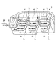
各検出機器20は、車両2に設けられ、検出信号をRFIDリーダー10に送信する機器である。各検出機器20は、電力を蓄電するバッテリを備えておらず、RFIDリーダー10から送信される電力供給用の信号(電力ともいう。)を動力として起動するパッシブ方式のRFIDを用いた機器である。各検出機器20は、車両2の異なる場所にそれぞれ設けられる。各検出機器20は、例えば、図3及び図4に示すように、車両2の複数の座席2aにそれぞれ設けられる。各検出機器20は、例えば、座席2aの座面部2bに設けられる。 Each detection device 20 is provided in the vehicle 2 and transmits a detection signal to the RFID reader 10 . Each detection device 20 does not have a battery for storing electric power, and is a device using a passive RFID that is powered by a power supply signal (also referred to as electric power) transmitted from the RFID reader 10. . Each detection device 20 is provided at a different location on the vehicle 2 . Each detection device 20 is provided on each of a plurality of seats 2a of the vehicle 2, as shown in FIGS. 3 and 4, for example. Each detection device 20 is provided, for example, on the seat surface portion 2b of the seat 2a.

各検出機器20は、アンテナとしてのループアンテナ21と、利得低減部としてのスイッチ部22と、信号出力部としてのRFID検出回路23とを備える。ループアンテナ21は、RFIDリーダー10との間で相互に信号を送受信するものである。ループアンテナ21は、アンテナ導体が1回又は複数回、環状に巻き回されて形成される。ループアンテナ21は、巻き回し開始側の始端部21aと巻き回し終了側の終端部21bとを含んで構成される(図1参照)。ループアンテナ21は、スイッチ部22を介してRFID検出回路23に接続される。ループアンテナ21は、例えば、始端部21aが後述する第1スイッチ回路22Rに接続され、終端部21bが第2スイッチ回路22Lに接続される。ループアンテナ21は、第1及び第2スイッチ回路22R、22Lが接続状態(オン)の場合、RFIDリーダー10から送信された電力供給用の信号、及び、搬送波を含む送信信号を受信する。そして、ループアンテナ21は、受信した送信信号を第1及び第2スイッチ回路22R、22Lを介してRFID検出回路23に出力する。そして、ループアンテナ21は、RFID検出回路23から第1及び第2スイッチ回路22R、22Lを介して出力される検出信号をRFIDリーダー10に送信する。一方、ループアンテナ21は、第1及び第2スイッチ回路22R、22Lが非接続状態(オフ)の場合、RFIDリーダー10から送信された電力供給用の信号、及び、搬送波を含む送信信号を受信しない。 Each detection device 20 includes a loop antenna 21 as an antenna, a switch section 22 as a gain reduction section, and an RFID detection circuit 23 as a signal output section. The loop antenna 21 exchanges signals with the RFID reader 10 . The loop antenna 21 is formed by winding an antenna conductor once or multiple times into a ring. The loop antenna 21 includes a winding starting end portion 21a and a winding ending end portion 21b (see FIG. 1). Loop antenna 21 is connected to RFID detection circuit 23 via switch section 22 . The loop antenna 21 has, for example, a starting end 21a connected to a first switching circuit 22R, which will be described later, and a terminating end 21b connected to a second switching circuit 22L. When the first and second switch circuits 22R and 22L are in a connected state (ON), the loop antenna 21 receives a power supply signal and a transmission signal including carrier waves transmitted from the RFID reader 10 . The loop antenna 21 then outputs the received transmission signal to the RFID detection circuit 23 via the first and second switch circuits 22R and 22L. Then, the loop antenna 21 transmits a detection signal output from the RFID detection circuit 23 through the first and second switch circuits 22R and 22L to the RFID reader 10 . On the other hand, when the first and second switch circuits 22R and 22L are in a non-connected state (OFF), the loop antenna 21 does not receive the power supply signal and the transmission signal including the carrier wave transmitted from the RFID reader 10. .

スイッチ部22は、押しボタン式やスライド式等のスイッチである。スイッチ部22は、第1スイッチ回路22Rと、第2スイッチ回路22Lとを含んで構成される。第1スイッチ回路22Rは、電気的な接続をオン又はオフに切り替えるものである。第1スイッチ回路22Rは、RFID検出回路23の第1回路端子23aとループアンテナ21の始端部21aとの間に設けられる。第1スイッチ回路22Rは、第1端子としてのスイッチ端子22aと、第2端子としてのスイッチ端子22bと、切替バー22cとを含んで構成される。スイッチ端子22a、22bは、ループアンテナ21の利得を低減するための第1作用点として機能するものである。スイッチ端子22a、22bは、RFID検出回路23の第1回路端子23aからループアンテナ21の第1延在方向に沿ってλ/8離れた位置までのループアンテナ21上の範囲K1内に位置する。ここで、「λ」は、ループアンテナ21により受信する電波の波長である。スイッチ端子22aは、RFID検出回路23の第1回路端子23aに接続されている。スイッチ端子22bは、ループアンテナ21の始端部21aに接続されている。切替バー22cは、スイッチ端子22a、22bを互いに電気的に接続状態(オン)又は非接続状態(オフ)に切り替える。つまり、切替バー22cは、RFID検出回路23の第1回路端子23aとループアンテナ21の始端部21aとを通電状態又は非通電状態に切り替える。 The switch unit 22 is a switch of a push button type, a slide type, or the like. The switch section 22 includes a first switch circuit 22R and a second switch circuit 22L. The first switch circuit 22R switches electrical connection on or off. The first switch circuit 22</b>R is provided between the first circuit terminal 23 a of the RFID detection circuit 23 and the leading end 21 a of the loop antenna 21 . The first switch circuit 22R includes a switch terminal 22a as a first terminal, a switch terminal 22b as a second terminal, and a switching bar 22c. The switch terminals 22a and 22b function as a first action point for reducing the gain of the loop antenna 21. FIG. The switch terminals 22 a and 22 b are located within a range K 1 on the loop antenna 21 from the first circuit terminal 23 a of the RFID detection circuit 23 to a position separated by λ/8 along the first extending direction of the loop antenna 21 . Here, “λ” is the wavelength of radio waves received by the loop antenna 21 . The switch terminal 22 a is connected to the first circuit terminal 23 a of the RFID detection circuit 23 . The switch terminal 22b is connected to the starting end 21a of the loop antenna 21 . The switching bar 22c switches the switch terminals 22a and 22b to an electrically connected state (ON) or a disconnected state (OFF). That is, the switching bar 22c switches the first circuit terminal 23a of the RFID detection circuit 23 and the leading end portion 21a of the loop antenna 21 between the energized state and the non-energized state.

第2スイッチ回路22Lは、電気的な接続をオン又はオフに切り替えるものである。第2スイッチ回路22Lは、RFID検出回路23の第2回路端子23bとループアンテナ21の終端部21bとの間に設けられる。第2スイッチ回路22Lは、第3端子としてのスイッチ端子22dと、第4端子としてのスイッチ端子22eと、切替バー22fとを含んで構成される。スイッチ端子22d、22eは、ループアンテナ21の利得を低減するための第2作用点として機能するものである。スイッチ端子22d、22eは、RFID検出回路23の第2回路端子23bからループアンテナ21の第2延在方向に沿ってλ/8離れた位置までのループアンテナ21上の範囲K2内に位置する。スイッチ端子22dは、RFID検出回路23の第2回路端子23bに接続されている。スイッチ端子22eは、ループアンテナ21の終端部21bに接続されている。切替バー22fは、スイッチ端子22d、22eを互いに電気的に接続状態(オン)又は非接続状態(オフ)に切り替える。つまり、切替バー22fは、RFID検出回路23の第2回路端子23bとループアンテナ21の終端部21bとを通電状態又は非通電状態に切り替える。 The second switch circuit 22L switches the electrical connection on or off. The second switch circuit 22L is provided between the second circuit terminal 23b of the RFID detection circuit 23 and the terminal end 21b of the loop antenna 21. As shown in FIG. The second switch circuit 22L includes a switch terminal 22d as a third terminal, a switch terminal 22e as a fourth terminal, and a switching bar 22f. The switch terminals 22 d and 22 e function as a second point of action for reducing the gain of the loop antenna 21 . The switch terminals 22 d and 22 e are located within a range K 2 on the loop antenna 21 from the second circuit terminal 23 b of the RFID detection circuit 23 to a position separated by λ/8 along the second extending direction of the loop antenna 21 . The switch terminal 22 d is connected to the second circuit terminal 23 b of the RFID detection circuit 23 . The switch terminal 22 e is connected to the terminal end 21 b of the loop antenna 21 . The switching bar 22f switches the switch terminals 22d and 22e to an electrically connected state (on) or a non-connected state (off). That is, the switching bar 22f switches the second circuit terminal 23b of the RFID detection circuit 23 and the terminal end portion 21b of the loop antenna 21 between the energized state and the non-energized state.

スイッチ部22は、検出対象である搭乗者の動作による外力が加えられている場合、第1及び第2スイッチ回路22R、22Lをオン又はオフの一方に設定する。また、スイッチ部22は、搭乗者の動作による外力が加えられていない場合、第1及び第2スイッチ回路22R、22Lをオン又はオフの他方に設定する。第1実施形態では、スイッチ部22は、外力が加えられている場合にはオンし、外力が加えられていない場合にはオフする(モーメンタリ動作)。スイッチ部22は、例えば、搭乗者が座席2aに着座した場合には搭乗者の押圧力によりオンに切り替え、搭乗者が座席2aに着座していない場合には搭乗者の押圧力から解放されることによりオフに切り替える。 The switch unit 22 sets the first and second switch circuits 22R and 22L to one of ON and OFF when an external force is applied by the movement of the passenger, which is the object of detection. Further, the switch unit 22 sets the first and second switch circuits 22R and 22L to the other of ON or OFF when no external force is applied by the passenger's motion. In the first embodiment, the switch section 22 is turned on when an external force is applied, and turned off when no external force is applied (momentary operation). For example, the switch unit 22 is switched on by the pressing force of the passenger when the passenger is seated on the seat 2a, and is released from the pressing force of the passenger when the passenger is not seated on the seat 2a. switch off by

スイッチ部22は、例えば、搭乗者が座席2aに着座していない場合、第1スイッチ回路22Rのスイッチ端子22a、22bを非接続状態(オフ)とし、且つ、第2スイッチ回路22Lのスイッチ端子22d、22eを非接続状態(オフ)とすることで、ループアンテナ21の利得を低減する利得低減状態に切り替える。つまり、スイッチ部22は、搭乗者が座席2aに着座していない場合、第1及び第2スイッチ回路22R、22Lをオフに切り替えてRFID検出回路23とループアンテナ21とのアンテナ整合を不一致状態とする。言い換えれば、スイッチ部22は、第1及び第2スイッチ回路22R、22Lをオフに切り替えてRFID検出回路23とループアンテナ21とのインピーダンスを不整合とする。これにより、検出機器20は、搭乗者が座席2aに着座していない場合、受信感度が低下してRFID検出回路23が起動しないようにできる。 For example, when the passenger is not seated on the seat 2a, the switch unit 22 sets the switch terminals 22a and 22b of the first switch circuit 22R to a non-connected state (off), and switches the switch terminal 22d of the second switch circuit 22L. , 22e are brought into a non-connected state (turned off), the loop antenna 21 is switched to a gain reduction state in which the gain is reduced. In other words, when the passenger is not seated on the seat 2a, the switch unit 22 switches off the first and second switch circuits 22R and 22L to set the antenna matching between the RFID detection circuit 23 and the loop antenna 21 to a mismatched state. do. In other words, the switch unit 22 switches off the first and second switch circuits 22R and 22L to make the impedances of the RFID detection circuit 23 and the loop antenna 21 mismatch. As a result, when the passenger is not seated on the seat 2a, the detection device 20 can prevent the RFID detection circuit 23 from activating due to the reduced reception sensitivity.

一方、スイッチ部22は、搭乗者が座席2aに着座している場合、第1スイッチ回路22Rのスイッチ端子22a、22bを接続状態(オン)とし、且つ、第2スイッチ回路22Lのスイッチ端子22d、22eを接続状態(オン)とすることで、ループアンテナ21の利得を低減しない利得非低減状態に切り替える。つまり、スイッチ部22は、搭乗者が座席2aに着座している場合、第1及び第2スイッチ回路22R、22Lをオンに切り替えてRFID検出回路23とループアンテナ21とのアンテナ整合を一致状態とする。言い換えれば、スイッチ部22は、第1及び第2スイッチ回路22R、22Lをオンに切り替えてRFID検出回路23とループアンテナ21とのインピーダンスを整合させる。これにより、検出機器20は、搭乗者が座席2aに着座している場合、受信感度が低下しないのでRFIDリーダー10からの電力供給用の信号によりRFID検出回路23を起動することができる。 On the other hand, when the passenger is seated on the seat 2a, the switch unit 22 connects (turns on) the switch terminals 22a and 22b of the first switch circuit 22R, and switches the switch terminals 22d and 22d of the second switch circuit 22L. 22e is connected (turned on), the gain of the loop antenna 21 is switched to a non-reduction state in which the gain is not reduced. That is, when the passenger is seated on the seat 2a, the switch unit 22 switches on the first and second switch circuits 22R and 22L to bring the antenna matching between the RFID detection circuit 23 and the loop antenna 21 into a matching state. do. In other words, the switch unit 22 switches on the first and second switch circuits 22R and 22L to match the impedances of the RFID detection circuit 23 and the loop antenna 21 . As a result, when the passenger is seated on the seat 2a, the detecting device 20 can activate the RFID detecting circuit 23 by the power supply signal from the RFID reader 10 because the receiving sensitivity does not decrease.

RFID検出回路23は、検出信号を出力する回路である。ここで、検出信号は、検出機器20毎にそれぞれ異なる識別子(例えば番号、記号等)を含む信号である。RFID検出回路23は、RFIDリーダー10から送信された電力供給用の信号を動力として駆動し検出信号を生成する。RFID検出回路23は、例えば、第1及び第2回路端子23a、23bと、整流回路23cと、記憶部23dと、IC回路23eとを備える。第1及び第2回路端子23a、23bは、外部機器と電気的に接続される部分である。第1回路端子23aは、第1スイッチ回路22Rのスイッチ端子22aに接続され、第2回路端子23bは、第2スイッチ回路22Lのスイッチ端子22dに接続される。 The RFID detection circuit 23 is a circuit that outputs a detection signal. Here, the detection signal is a signal including an identifier (for example, number, symbol, etc.) different for each detection device 20 . The RFID detection circuit 23 is driven by a power supply signal transmitted from the RFID reader 10 to generate a detection signal. The RFID detection circuit 23 includes, for example, first and second circuit terminals 23a and 23b, a rectifier circuit 23c, a storage section 23d, and an IC circuit 23e. The first and second circuit terminals 23a and 23b are portions electrically connected to an external device. The first circuit terminal 23a is connected to the switch terminal 22a of the first switch circuit 22R, and the second circuit terminal 23b is connected to the switch terminal 22d of the second switch circuit 22L.

整流回路23cは、第1及び第2スイッチ回路22R、22L等を介してループアンテナ21に接続され、ループアンテナ21から出力される交流電力(電力供給用の信号)を整流し直流電力を生成する。整流回路23cは、記憶部23d及びIC回路23eに接続され、生成した直流電力を図示しない平滑回路を介して記憶部23d及びIC回路23eに供給する。 The rectifier circuit 23c is connected to the loop antenna 21 via the first and second switch circuits 22R, 22L, etc., and rectifies the AC power (signal for power supply) output from the loop antenna 21 to generate DC power. . The rectifying circuit 23c is connected to the storage unit 23d and the IC circuit 23e, and supplies the generated DC power to the storage unit 23d and the IC circuit 23e via a smoothing circuit (not shown).

記憶部23dは、検出機器20毎にそれぞれ異なる識別子を記憶する回路である。記憶部23dは、IC回路23eに接続され、当該IC回路23eにより識別子が参照される。 The storage unit 23 d is a circuit that stores identifiers that are different for each detecting device 20 . The storage unit 23d is connected to the IC circuit 23e, and the identifier is referred to by the IC circuit 23e.

IC回路23eは、記憶部23d及びループアンテナ21に接続され、記憶部23dに記憶された識別子を取得し、取得した識別子に基づいて搬送波を変調した検出信号を第1及び第2スイッチ回路22R、22L等を介してループアンテナ21に出力する。 The IC circuit 23e is connected to the storage unit 23d and the loop antenna 21, acquires the identifier stored in the storage unit 23d, and transmits a detection signal obtained by modulating a carrier wave based on the acquired identifier to the first and second switch circuits 22R, 22R, and 22R. 22L or the like to the loop antenna 21.

ECU30は、車両2全体を制御する電子回路である。ECU30は、CPU、メモリを構成するROM、RAM及びインターフェースを含む周知のマイクロコンピュータを主体とする電子回路を含んで構成される。ECU30は、例えば、RFIDリーダー10に接続され、RFIDリーダー10が受信した検出信号に基づいて車両2内の検出対象の状態を判定する。ECU30は、検出信号に含まれる識別子と車両2内の検出対象の状態とを予め対応付けている。例えば、ECU30は、それぞれ異なる識別子と車両2の各座席2aとを対応付けている。これにより、ECU30は、識別子に基づいて各座席2aの状態を判定することができる。ECU30は、各検出機器20に電力供給用の信号、及び、搬送波を含む送信信号を所定間隔(例えば1秒間隔)で送信するように送信部11aを制御する。 The ECU 30 is an electronic circuit that controls the vehicle 2 as a whole. The ECU 30 includes an electronic circuit mainly composed of a well-known microcomputer including a CPU, a ROM constituting a memory, a RAM, and an interface. The ECU 30 , for example, is connected to the RFID reader 10 and determines the state of the object to be detected inside the vehicle 2 based on the detection signal received by the RFID reader 10 . The ECU 30 associates the identifier included in the detection signal with the state of the object to be detected inside the vehicle 2 in advance. For example, the ECU 30 associates each different identifier with each seat 2a of the vehicle 2 . Thereby, the ECU 30 can determine the state of each seat 2a based on the identifier. The ECU 30 controls the transmitter 11a to transmit a signal for power supply and a transmission signal including a carrier wave to each detection device 20 at predetermined intervals (for example, at intervals of one second).

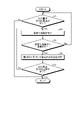
次に、図5を参照して検出システム1の動作例について説明する。検出システム1のECU30は、ACC(アクセサリー)電源又はIG(イグニッション)電源がオンであるか否かを判定する(ステップS1)。ECU30は、ACC電源又はIG電源がオンである場合(ステップS1;Yes)、RFIDリーダー10により各検出機器20を検出する(ステップS2)。例えば、ECU30は、RFIDリーダー10から各検出機器20に電力供給用の信号、及び、搬送波を含む送信信号を所定間隔(例えば1秒間隔)で送信する。次に、ECU30は、各検出機器20から返答があるか否かを判定する(ステップS3)。各検出機器20は、搭乗者の動作による外力が加えられ第1及び第2スイッチ回路22R、22Lがオンである場合、RFID検出回路23とループアンテナ21とが電気的に接続され、ループアンテナ21の利得が低減されないので起動する。この場合、各検出機器20は、RFID検出回路23からループアンテナ21を介して検出信号をRFIDリーダー10に送信する。また、各検出機器20は、搭乗者の動作による外力が加えられず第1及び第2スイッチ回路22R、22Lがオフである場合、RFID検出回路23とループアンテナ21との電気的な接続を遮断し、ループアンテナ21の利得が低減されるので起動しない。この場合、各検出機器20は、RFID検出回路23からループアンテナ21を介して検出信号をRFIDリーダー10に送信しない。 Next, an operation example of the detection system 1 will be described with reference to FIG. The ECU 30 of the detection system 1 determines whether or not an ACC (accessory) power supply or an IG (ignition) power supply is on (step S1). When the ACC power supply or the IG power supply is on (step S1; Yes), the ECU 30 detects each detection device 20 by the RFID reader 10 (step S2). For example, the ECU 30 transmits a power supply signal and a transmission signal including a carrier wave from the RFID reader 10 to each detection device 20 at predetermined intervals (for example, 1 second interval). Next, the ECU 30 determines whether or not there is a reply from each detecting device 20 (step S3). In each detection device 20, when an external force is applied by the movement of the passenger and the first and second switch circuits 22R and 22L are turned on, the RFID detection circuit 23 and the loop antenna 21 are electrically connected, and the loop antenna 21 is turned on. gain is not reduced. In this case, each detection device 20 transmits a detection signal from the RFID detection circuit 23 to the RFID reader 10 via the loop antenna 21 . In addition, each detection device 20 cuts off the electrical connection between the RFID detection circuit 23 and the loop antenna 21 when the first and second switch circuits 22R and 22L are off without an external force due to the movement of the passenger. However, since the gain of the loop antenna 21 is reduced, it does not start. In this case, each detection device 20 does not transmit a detection signal from the RFID detection circuit 23 to the RFID reader 10 via the loop antenna 21 .

RFIDリーダー10は、各検出機器20から検出信号を受信すると、受信した検出信号の識別子をECU30に出力する。ECU30は、RFIDリーダー10から識別子が出力されると各検出機器20から返答があったと判定する。ECU30は、各検出機器20から返答があったと判定した場合(ステップS3;Yes)、識別子に基づいて車両2内の検出対象の状態を判定する(ステップS4)。例えば、ECU30は、RFIDリーダー10から出力された識別子に対応付けられた座席2aに搭乗者が着座したと判定する。次に、ECU30は、ACC電源又はIG電源がオフであるか否かを判定する(ステップS5)。ECU30は、ACC電源又はIG電源がオフである場合(ステップS5;Yes)、処理を終了する。また、ECU30は、ACC電源又はIG電源がオンである場合(ステップS5;No)、上述のステップS2に戻り、RFIDリーダー10により各検出機器20を検出する。なお、上述のステップS1で、ECU30は、ACC電源又はIG電源がオフである場合(ステップS1;No)、処理を終了する。また、上述のステップS3で、ECU30は、各検出機器20から返答がなかった場合(ステップS3;No)、再度、RFIDリーダー10により各検出機器20を検出する(ステップS1、S2)。 Upon receiving the detection signal from each detection device 20 , the RFID reader 10 outputs the identifier of the received detection signal to the ECU 30 . The ECU 30 determines that each detection device 20 has responded when the identifier is output from the RFID reader 10 . When the ECU 30 determines that there is a response from each detection device 20 (step S3; Yes), the ECU 30 determines the state of the detection target inside the vehicle 2 based on the identifier (step S4). For example, the ECU 30 determines that the passenger has sat on the seat 2a associated with the identifier output from the RFID reader 10 . Next, the ECU 30 determines whether or not the ACC power supply or the IG power supply is off (step S5). When the ACC power supply or the IG power supply is off (step S5; Yes), the ECU 30 ends the process. Further, when the ACC power supply or the IG power supply is on (step S5; No), the ECU 30 returns to the above-described step S2 and detects each detection device 20 by the RFID reader 10. FIG. In step S1 described above, the ECU 30 terminates the process if the ACC power supply or the IG power supply is off (step S1; No). If there is no response from each detection device 20 in step S3 described above (step S3; No), the ECU 30 again detects each detection device 20 using the RFID reader 10 (steps S1 and S2).

以上のように、第1実施形態に係る検出機器20は、ループアンテナ21と、RFID検出回路23と、スイッチ部22とを備える。ループアンテナ21は、信号を含む電波を送受信する。RFID検出回路23は、ループアンテナ21に接続される第1回路端子23a及び第2回路端子23bを含んで構成される。RFID検出回路23は、ループアンテナ21により受信した信号に含まれる電力供給用の信号を動力として起動し検出信号をループアンテナ21に出力する。スイッチ部22は、検出対象の状態に応じてループアンテナ21の利得を低減する利得低減状態又はループアンテナ21の利得を低減しない利得非低減状態に切り替える。ここで、スイッチ部22は、電波の波長をλとしたとき、第1回路端子23aからループアンテナ21の第1延在方向に沿ってλ/8離れた位置までのループアンテナ21上の範囲K1内にループアンテナ21の利得を低減するためのスイッチ端子22a、22bを有する。スイッチ部22は、さらに、第2回路端子23bからループアンテナ21の第2延在方向に沿ってλ/8離れた位置までのループアンテナ21上の範囲K2内にループアンテナ21の利得を低減するためのスイッチ端子22d、22eを有する。 As described above, the detection device 20 according to the first embodiment includes the loop antenna 21 , the RFID detection circuit 23 and the switch section 22 . The loop antenna 21 transmits and receives radio waves including signals. The RFID detection circuit 23 includes a first circuit terminal 23 a and a second circuit terminal 23 b connected to the loop antenna 21 . The RFID detection circuit 23 is activated by a power supply signal included in the signal received by the loop antenna 21 and outputs a detection signal to the loop antenna 21 . The switch unit 22 switches between a gain reduction state in which the gain of the loop antenna 21 is reduced or a gain non-reduction state in which the gain of the loop antenna 21 is not reduced, depending on the state of the detection target. Here, when the wavelength of the radio wave is λ, the switch unit 22 has a range K1 on the loop antenna 21 from the first circuit terminal 23a to a position separated by λ/8 along the first extending direction of the loop antenna 21. It has switch terminals 22a and 22b for reducing the gain of the loop antenna 21 therein. The switch unit 22 further reduces the gain of the loop antenna 21 within a range K2 on the loop antenna 21 from the second circuit terminal 23b to a position separated by λ/8 along the second extending direction of the loop antenna 21. has switch terminals 22d and 22e for

この構成により、検出機器20は、検出対象の状態に応じてループアンテナ21とRFID検出回路23とを電気的に完全に切り離すことができる。これにより、検出機器20は、RFID検出回路23及びループアンテナ21のインピーダンスを不整合とすることができ、ループアンテナ21の利得を低減する利得低減状態を実現することができる。これにより、検出機器20は、ループアンテナ21の受信感度を低下させ当該ループアンテナ21を無効化することができ、電力供給用の信号が送信されてもRFID検出回路23を起動させないようにできる。また、検出機器20は、検出対象の状態に応じてループアンテナ21とRFID検出回路23とを電気的に接続することができる。これにより、検出機器20は、RFID検出回路23及びループアンテナ21のインピーダンスを整合させることができ、ループアンテナ21の利得を低減しない利得非低減状態を実現することができる。これにより、検出機器20は、ループアンテナ21の受信感度を低下させないので当該ループアンテナ21を有効化することができ、電力供給用の信号によりRFID検出回路23を起動させることができる。この結果、検出機器20は、例えば、搭乗者が座席2aに着座していないにも関わらず検出信号を出力するような誤検出を抑制することができ、検出対象の検出精度を向上することができる。検出機器20は、スイッチ端子22a、22dをそれぞれ第1及び第2回路端子23a、23bに直接接続することでRFID検出回路23の両端部に残る導体長を短くし、RFID検出回路23の受信感度をより低下させることができる。これにより、検出機器20は、RFIDリーダー10との距離を相対的に短くすることができ、検出領域を拡大することができる。 With this configuration, the detection device 20 can completely electrically disconnect the loop antenna 21 and the RFID detection circuit 23 according to the state of the object to be detected. Thereby, the detection device 20 can make the impedances of the RFID detection circuit 23 and the loop antenna 21 mismatch, and can realize a gain reduction state in which the gain of the loop antenna 21 is reduced. As a result, the detection device 20 can reduce the reception sensitivity of the loop antenna 21 to disable the loop antenna 21, and can prevent the RFID detection circuit 23 from being activated even if a power supply signal is transmitted. Further, the detection device 20 can electrically connect the loop antenna 21 and the RFID detection circuit 23 according to the state of the object to be detected. As a result, the detection device 20 can match the impedances of the RFID detection circuit 23 and the loop antenna 21, and realize a gain non-reduction state in which the gain of the loop antenna 21 is not reduced. As a result, the detection device 20 can activate the loop antenna 21 because the reception sensitivity of the loop antenna 21 is not lowered, and the RFID detection circuit 23 can be activated by the power supply signal. As a result, the detection device 20 can suppress erroneous detection, for example, outputting a detection signal even though the passenger is not seated on the seat 2a, and can improve the detection accuracy of the detection target. can. The detection device 20 shortens the conductor length remaining at both ends of the RFID detection circuit 23 by directly connecting the switch terminals 22a and 22d to the first and second circuit terminals 23a and 23b, respectively, thereby increasing the reception sensitivity of the RFID detection circuit 23. can be further reduced. As a result, the detection device 20 can relatively shorten the distance to the RFID reader 10 and expand the detection area.

上記検出機器20において、スイッチ端子22a、22b、22d、22eは、RFID検出回路23とループアンテナ21とを通電状態又は非通電状態にするための作用点である。この構成により、検出機器20は、検出対象の状態に応じてループアンテナ21とRFID検出回路23とを電気的に完全に切り離すことができ、利得低減状態を実現することができる。 In the detection device 20, the switch terminals 22a, 22b, 22d, and 22e are points of action for making the RFID detection circuit 23 and the loop antenna 21 conductive or non-conductive. With this configuration, the detection device 20 can completely electrically disconnect the loop antenna 21 and the RFID detection circuit 23 according to the state of the detection target, and can realize a gain reduction state.

上記検出機器20において、スイッチ部22は、スイッチ端子22a、22bを互いに電気的に接続状態又は非接続状態に切り替え可能な第1スイッチ回路22Rと、スイッチ端子22d、22eを互いに電気的に接続状態又は非接続状態に切り替え可能な第2スイッチ回路22Lとを含んで構成される。スイッチ部22は、スイッチ端子22a、22bを接続状態とし且つスイッチ端子22d、22eを接続状態とした利得非低減状態と、スイッチ端子22a、22bを非接続状態とし且つスイッチ端子22d、22eを非接続状態とした利得低減状態と、を切り替え可能である。この構成により、検出機器20は、検出対象の状態に応じてループアンテナ21とRFID検出回路23とを電気的に完全に切り離すことができ、利得低減状態を実現することができる。また、検出機器20は、検出対象の状態に応じてループアンテナ21とRFID検出回路23とを電気的に接続することができ、利得非低減状態を実現することができる。 In the detection device 20, the switch section 22 includes a first switch circuit 22R capable of switching the switch terminals 22a and 22b between electrically connected and non-connected states, and the switch terminals 22d and 22e electrically connected to each other. Alternatively, it includes a second switch circuit 22L that can be switched to a non-connected state. The switch section 22 has a gain non-reducing state in which the switch terminals 22a and 22b are connected and the switch terminals 22d and 22e are connected, and a gain non-reduction state in which the switch terminals 22a and 22b are in a non-connected state and the switch terminals 22d and 22e are not connected. It is possible to switch between a gain reduction state and a gain reduction state. With this configuration, the detection device 20 can completely electrically disconnect the loop antenna 21 and the RFID detection circuit 23 according to the state of the detection target, and can realize a gain reduction state. In addition, the detection device 20 can electrically connect the loop antenna 21 and the RFID detection circuit 23 according to the state of the object to be detected, and can realize the gain non-reduction state.

第1実施形態に係る検出システム1は、RFIDリーダー10と、検出機器20と、ECU30とを備える。RFIDリーダー10は、信号を含む電波を送受信し、少なくとも電力供給用の信号を含む送信信号を送信する。検出機器20は、ループアンテナ21、RFID検出回路23、及び、スイッチ部22を含んで構成される。ループアンテナ21は、RFIDリーダー10との間で相互に信号を送受信する。RFID検出回路23は、ループアンテナ21に接続される第1回路端子23a及び第2回路端子23bを有し、ループアンテナ21により受信した信号に含まれる電力供給用の信号を動力として起動し、検出信号をループアンテナ21に出力する。スイッチ部22は、検出対象の状態に応じてループアンテナ21の利得を低減する利得低減状態又はループアンテナ21の利得を低減しない利得非低減状態に切り替える。ECU30は、RFIDリーダー10に接続され、当該RFIDリーダー10が受信した検出信号に基づいて検出対象の状態を判定する。ここで、スイッチ部22は、電波の波長をλとしたとき、第1回路端子23aからループアンテナ21の第1延在方向に沿ってλ/8離れた位置までのループアンテナ21上の範囲K1内にループアンテナ21の利得を低減するためのスイッチ端子22a、22bを有する。スイッチ部22は、さらに、第2回路端子23bからループアンテナ21の第2延在方向に沿ってλ/8離れた位置までのループアンテナ21上の範囲K2内にループアンテナ21の利得を低減するためのスイッチ端子22d、22eを有する。この構成により、検出システム1は、上述の検出機器20と同等の効果を奏することができる。 A detection system 1 according to the first embodiment includes an RFID reader 10 , a detection device 20 and an ECU 30 . The RFID reader 10 transmits and receives radio waves including signals, and transmits transmission signals including at least power supply signals. The detection device 20 includes a loop antenna 21 , an RFID detection circuit 23 and a switch section 22 . The loop antenna 21 mutually transmits and receives signals to and from the RFID reader 10 . The RFID detection circuit 23 has a first circuit terminal 23a and a second circuit terminal 23b connected to the loop antenna 21, and is activated by a power supply signal included in the signal received by the loop antenna 21, and detects The signal is output to loop antenna 21 . The switch unit 22 switches between a gain reduction state in which the gain of the loop antenna 21 is reduced or a gain non-reduction state in which the gain of the loop antenna 21 is not reduced, depending on the state of the detection target. The ECU 30 is connected to the RFID reader 10 and determines the state of the object to be detected based on the detection signal received by the RFID reader 10 . Here, when the wavelength of the radio wave is λ, the switch unit 22 has a range K1 on the loop antenna 21 from the first circuit terminal 23a to a position separated by λ/8 along the first extending direction of the loop antenna 21. It has switch terminals 22a and 22b for reducing the gain of the loop antenna 21 therein. The switch unit 22 further reduces the gain of the loop antenna 21 within a range K2 on the loop antenna 21 from the second circuit terminal 23b to a position separated by λ/8 along the second extending direction of the loop antenna 21. has switch terminals 22d and 22e for With this configuration, the detection system 1 can achieve effects equivalent to those of the detection device 20 described above.

〔第1実施形態の変形例〕
次に、図6を参照して、第1実施形態の第1変形例に係る検出機器20Aについて説明する。なお、第1実施形態の第1変形例では、第1実施形態と同等の構成要素には同じ符号を付し、その詳細な説明を省略する。検出機器20Aは、第1及び第2スイッチ回路22R、22Lが電線26A、26Bを介してループアンテナ21に接続される点で第1実施形態の検出機器20とは異なる。検出機器20Aは、ループアンテナ21と、第1及び第2スイッチ回路22R、22Lと、電線26A、26Bと、RFID検出回路23とを備える。電線26Aは、2本の導体26aと、各導体26aを被覆する被覆部26bとを含んで構成される。各導体26aは、延在方向に沿って延在する。一方の導体26aは、一端がRFID検出回路23の第1回路端子23aに接続され、他端が第1スイッチ回路22Rのスイッチ端子22aに接続される。他方の導体26aは、一端がループアンテナ21の始端部21aに接続され、他端が第1スイッチ回路22Rのスイッチ端子22bに接続される。各導体26aは、延在方向に交差する方向において互いに隣接して配置される。各導体26aは、互いに隣接して配置されることにより、各電流経路を流れる電流により生じる少なくとも一部の磁界を互いに打ち消し合う。つまり、各導体26aは、一方の電流経路に流れる電流と他方の電流経路に流れる電流とが互いに反対向きに流れることにより磁界を互いに打ち消し合う。これにより、各導体26aは、ループアンテナ21に与える磁界の影響を抑制することができる。
[Modification of First Embodiment]
Next, a detection device 20A according to a first modified example of the first embodiment will be described with reference to FIG. In addition, in the first modified example of the first embodiment, the same reference numerals are given to the same constituent elements as in the first embodiment, and detailed description thereof will be omitted. The detection device 20A differs from the detection device 20 of the first embodiment in that the first and second switch circuits 22R and 22L are connected to the loop antenna 21 via electric wires 26A and 26B. The detection device 20A includes a loop antenna 21, first and second switch circuits 22R and 22L, electric wires 26A and 26B, and an RFID detection circuit 23. 26 A of electric wires are comprised including the two conductors 26a and the coating part 26b which coat|covers each conductor 26a. Each conductor 26a extends along the extension direction. One conductor 26a has one end connected to the first circuit terminal 23a of the RFID detection circuit 23 and the other end connected to the switch terminal 22a of the first switch circuit 22R. The other conductor 26a has one end connected to the starting end 21a of the loop antenna 21 and the other end connected to the switch terminal 22b of the first switch circuit 22R. Each conductor 26a is arranged adjacent to each other in a direction intersecting the extending direction. The conductors 26a are arranged adjacent to each other so that at least some of the magnetic fields generated by the currents flowing through the respective current paths cancel each other out. In other words, in each conductor 26a, the current flowing in one current path and the current flowing in the other current path flow in opposite directions, thereby canceling out the magnetic fields. Thereby, each conductor 26 a can suppress the influence of the magnetic field on the loop antenna 21 .

同様に、電線26Bは、2本の導体26cと、各導体26cを被覆する被覆部26dとを含んで構成される。各導体26cは、延在方向に沿って延在する。一方の導体26cは、一端がRFID検出回路23の第2回路端子23bに接続され、他端が第2スイッチ回路22Lのスイッチ端子22dに接続される。他方の導体26cは、一端がループアンテナ21の終端部21bに接続され、他端が第2スイッチ回路22Lのスイッチ端子22eに接続される。各導体26cは、延在方向に交差する方向において互いに隣接して配置される。各導体26cは、互いに隣接して配置されることにより、各電流経路を流れる電流により生じる少なくとも一部の磁界を互いに打ち消し合う。つまり、各導体26cは、一方の電流経路に流れる電流と他方の電流経路に流れる電流とが互いに反対向きに流れることにより磁界を互いに打ち消し合う。これにより、各導体26cは、ループアンテナ21に与える磁界の影響を抑制することができる。 Similarly, the electric wire 26B includes two conductors 26c and a covering portion 26d covering each conductor 26c. Each conductor 26c extends along the extension direction. One conductor 26c has one end connected to the second circuit terminal 23b of the RFID detection circuit 23 and the other end connected to the switch terminal 22d of the second switch circuit 22L. The other conductor 26c has one end connected to the terminal end 21b of the loop antenna 21 and the other end connected to the switch terminal 22e of the second switch circuit 22L. Each conductor 26c is arranged adjacent to each other in a direction crossing the extending direction. The conductors 26c are arranged adjacent to each other so that at least some of the magnetic fields generated by the currents flowing through the respective current paths cancel each other out. In other words, in each conductor 26c, the current flowing through one current path and the current flowing through the other current path flow in opposite directions, thereby canceling out the magnetic fields. Thereby, each conductor 26 c can suppress the influence of the magnetic field on the loop antenna 21 .

以上のように、第1実施形態の第1変形例に係る検出機器20Aは、第1及び第2スイッチ回路22R、22Lが電線26A、26Bを介してループアンテナ21に接続される。この構成により、検出機器20Aは、第1及び第2スイッチ回路22R、22Lをループアンテナ21から離して設置することができ、設計の自由度を向上できる。また、検出機器20Aは、電線26A、26Bの磁界がループアンテナ21のアンテナ特性に与える影響を抑制できるので、ループアンテナ21の性能の低下を抑制できる。 As described above, in the detection device 20A according to the first modification of the first embodiment, the first and second switch circuits 22R and 22L are connected to the loop antenna 21 via the electric wires 26A and 26B. With this configuration, in the detection device 20A, the first and second switch circuits 22R and 22L can be installed away from the loop antenna 21, and the degree of freedom in design can be improved. In addition, since the detecting device 20A can suppress the influence of the magnetic fields of the electric wires 26A and 26B on the antenna characteristics of the loop antenna 21, deterioration of the performance of the loop antenna 21 can be suppressed.

次に、図7を参照して、第1実施形態の第2変形例に係る検出機器20Bについて説明する。検出機器20Bは、第1及び第2スイッチ回路22R、22Lが同軸ケーブル27A、27Bを介してループアンテナ21に接続される点で第1実施形態の検出機器20とは異なる。検出機器20Bは、ループアンテナ21と、第1及び第2スイッチ回路22R、22Lと、同軸ケーブル27A、27Bと、RFID検出回路23とを備える。同軸ケーブル27Aは、芯線27aと、当該芯線27aと同心円状に設けられるシールド編組27bと、芯線27a及びシールド編組27bを絶縁する絶縁体(図示省略)とを含んで構成される。同軸ケーブル27Aは、延在方向に沿って延在する。芯線27aは、一端がRFID検出回路23の第1回路端子23aに接続され、他端が第1スイッチ回路22Rのスイッチ端子22aに接続される。シールド編組27bは、一端がループアンテナ21の始端部21aに接続され、他端が第1スイッチ回路22Rのスイッチ端子22bに接続される。同軸ケーブル27Aは、電流が流れる際の磁界をシールド編組27bの内側に閉じ込めるため、ループアンテナ21に与える磁界の影響を抑制することができる。 Next, a detection device 20B according to a second modification of the first embodiment will be described with reference to FIG. The detection device 20B differs from the detection device 20 of the first embodiment in that the first and second switch circuits 22R and 22L are connected to the loop antenna 21 via coaxial cables 27A and 27B. The detection device 20B includes a loop antenna 21, first and second switch circuits 22R, 22L, coaxial cables 27A, 27B, and an RFID detection circuit 23. The coaxial cable 27A includes a core wire 27a, a shield braid 27b provided concentrically with the core wire 27a, and an insulator (not shown) that insulates the core wire 27a and the shield braid 27b. The coaxial cable 27A extends along the extension direction. The core wire 27a has one end connected to the first circuit terminal 23a of the RFID detection circuit 23 and the other end connected to the switch terminal 22a of the first switch circuit 22R. The shield braid 27b has one end connected to the starting end 21a of the loop antenna 21 and the other end connected to the switch terminal 22b of the first switch circuit 22R. Since the coaxial cable 27A confines the magnetic field generated when current flows inside the shield braid 27b, the influence of the magnetic field on the loop antenna 21 can be suppressed.

同様に、同軸ケーブル27Bは、芯線27cと、当該芯線27cと同心円状に設けられるシールド編組27dと、芯線27c及びシールド編組27dを絶縁する絶縁体(図示省略)とを含んで構成される。同軸ケーブル27Bは、延在方向に沿って延在する。芯線27cは、一端がRFID検出回路23の第2回路端子23bに接続され、他端が第2スイッチ回路22Lのスイッチ端子22eに接続される。シールド編組27dは、一端がループアンテナ21の終端部21bに接続され、他端が第2スイッチ回路22Lのスイッチ端子22dに接続される。同軸ケーブル27Bは、電流が流れる際の磁界をシールド編組27dの内側に閉じ込めるため、ループアンテナ21に与える磁界の影響を抑制することができる。 Similarly, the coaxial cable 27B includes a core wire 27c, a shield braid 27d provided concentrically with the core wire 27c, and an insulator (not shown) that insulates the core wire 27c and the shield braid 27d. The coaxial cable 27B extends along the extension direction. The core wire 27c has one end connected to the second circuit terminal 23b of the RFID detection circuit 23 and the other end connected to the switch terminal 22e of the second switch circuit 22L. The shield braid 27d has one end connected to the terminal end 21b of the loop antenna 21 and the other end connected to the switch terminal 22d of the second switch circuit 22L. Since the coaxial cable 27B confines the magnetic field generated when current flows inside the shield braid 27d, the influence of the magnetic field on the loop antenna 21 can be suppressed.

以上のように、第1実施形態の第2変形例に係る検出機器20Bは、第1及び第2スイッチ回路22R、22Lが同軸ケーブル27A、27Bを介してループアンテナ21に接続される。この構成により、検出機器20Bは、第1及び第2スイッチ回路22R、22Lをループアンテナ21から離して設置することができ、設計の自由度を向上できる。また、検出機器20Bは、同軸ケーブル27A、27Bの磁界がループアンテナ21のアンテナ特性に与える影響を抑制できるので、ループアンテナ21の性能の低下を抑制できる。 As described above, in the detection device 20B according to the second modification of the first embodiment, the first and second switch circuits 22R and 22L are connected to the loop antenna 21 via the coaxial cables 27A and 27B. With this configuration, the detection device 20B can install the first and second switch circuits 22R and 22L away from the loop antenna 21, thereby improving the degree of freedom in design. Further, since the detecting device 20B can suppress the influence of the magnetic fields of the coaxial cables 27A and 27B on the antenna characteristics of the loop antenna 21, it is possible to suppress deterioration of the performance of the loop antenna 21. FIG.

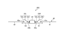
次に、図8を参照して、第1実施形態の第3変形例に係る検出機器20Cについて説明する。検出機器20Cは、ループアンテナ21の代わりにダイポールアンテナ40を備える点で第1実施形態の検出機器20とは異なる。検出機器20Cは、ダイポールアンテナ40と、第1及び第2スイッチ回路22R、22Lと、RFID検出回路23とを備える。ダイポールアンテナ40は、第1エレメント41及び第2エレメント42を含んで構成され、信号を含む電波を送受信するものである。第1スイッチ回路22Rは、RFID検出回路23の第1回路端子23aと第1エレメント41の一端41aとの間に設けられる。第1スイッチ回路22Rのスイッチ端子22a、22bは、RFID検出回路23の第1回路端子23aからダイポールアンテナ40の第1延在方向に沿ってλ/8離れた位置までのダイポールアンテナ40上の範囲K1内に位置する。ここで、「λ」は、ダイポールアンテナ40により受信する電波の波長である。第1スイッチ回路22Rは、スイッチ端子22aがRFID検出回路23の第1回路端子23aに接続され、スイッチ端子22bが第1エレメント41の一端41aに接続されている。第1スイッチ回路22Rは、RFID検出回路23の第1回路端子23aと第1エレメント41の一端41aとを通電状態又は非通電状態に切り替える。 Next, a detection device 20C according to a third modified example of the first embodiment will be described with reference to FIG. The detection device 20C differs from the detection device 20 of the first embodiment in that a dipole antenna 40 is provided instead of the loop antenna 21. FIG. The detection device 20C comprises a dipole antenna 40, first and second switch circuits 22R, 22L, and an RFID detection circuit 23. The dipole antenna 40 includes a first element 41 and a second element 42, and transmits and receives radio waves including signals. The first switch circuit 22 R is provided between the first circuit terminal 23 a of the RFID detection circuit 23 and the one end 41 a of the first element 41 . The switch terminals 22a and 22b of the first switch circuit 22R cover the range above the dipole antenna 40 from the first circuit terminal 23a of the RFID detection circuit 23 to a position separated by λ/8 along the first extending direction of the dipole antenna 40. Located within K1. Here, “λ” is the wavelength of radio waves received by the dipole antenna 40 . The first switch circuit 22 R has a switch terminal 22 a connected to the first circuit terminal 23 a of the RFID detection circuit 23 and a switch terminal 22 b connected to one end 41 a of the first element 41 . The first switch circuit 22R switches the first circuit terminal 23a of the RFID detection circuit 23 and the one end 41a of the first element 41 between an energized state and a non-energized state.

第2スイッチ回路22Lは、RFID検出回路23の第2回路端子23bと第2エレメント42の一端42aとの間に設けられる。第2スイッチ回路22Lのスイッチ端子22d、22eは、RFID検出回路23の第2回路端子23bからダイポールアンテナ40の第2延在方向に沿ってλ/8離れた位置までのダイポールアンテナ40上の範囲K2内に位置する。第2スイッチ回路22Lは、スイッチ端子22dがRFID検出回路23の第2回路端子23bに接続され、スイッチ端子22eが第2エレメント42の一端42aに接続されている。第2スイッチ回路22Lは、RFID検出回路23の第2回路端子23bと第2エレメント42の一端42aとを通電状態又は非通電状態に切り替える。 The second switch circuit 22L is provided between the second circuit terminal 23b of the RFID detection circuit 23 and the one end 42a of the second element 42 . The switch terminals 22d and 22e of the second switch circuit 22L extend over the dipole antenna 40 from the second circuit terminal 23b of the RFID detection circuit 23 to a position separated by λ/8 along the second extending direction of the dipole antenna 40. Located within K2. The second switch circuit 22L has a switch terminal 22d connected to the second circuit terminal 23b of the RFID detection circuit 23 and a switch terminal 22e connected to one end 42a of the second element 42 . The second switch circuit 22L switches the second circuit terminal 23b of the RFID detection circuit 23 and the one end 42a of the second element 42 between an energized state and a non-energized state.

検出機器20Cは、例えば、検出対象の状態に応じて第1スイッチ回路22Rのスイッチ端子22a、22bを非接続状態(オフ)とし、且つ、第2スイッチ回路22Lのスイッチ端子22d、22eを非接続状態(オフ)とすることで、ダイポールアンテナ40の利得を低減する利得低減状態に切り替える。また、検出機器20Cは、検出対象の状態に応じて第1スイッチ回路22Rのスイッチ端子22a、22bを接続状態(オン)とし、且つ、第2スイッチ回路22Lのスイッチ端子22d、22eを接続状態(オン)とすることで、ダイポールアンテナ40の利得を低減しない利得非低減状態に切り替える。 For example, the detection device 20C brings the switch terminals 22a and 22b of the first switch circuit 22R into a non-connected state (OFF) and the switch terminals 22d and 22e of the second switch circuit 22L into a non-connected state, depending on the state of the object to be detected. By switching to the state (OFF), the dipole antenna 40 is switched to a gain reduction state in which the gain is reduced. In addition, the detection device 20C sets the switch terminals 22a and 22b of the first switch circuit 22R to the connected state (ON) and the switch terminals 22d and 22e of the second switch circuit 22L to the connected state ( ON), the gain of the dipole antenna 40 is switched to a non-reduction state in which the gain is not reduced.

以上のように、第1実施形態の第3変形例に係る検出機器20Cは、検出対象の状態に応じてダイポールアンテナ40とRFID検出回路23とを電気的に完全に切り離すことができる。これにより、検出機器20Cは、利得低減状態を実現することができ、ダイポールアンテナ40を無効化することができる。また、検出機器20Cは、検出対象の状態に応じてダイポールアンテナ40とRFID検出回路23とを電気的に接続することができる。これにより、検出機器20Cは、利得非低減状態を実現することができ、ダイポールアンテナ40を有効化することができる。この結果、検出機器20Cは、検出対象の検出精度を向上することができる。検出機器20Cは、スイッチ端子22a、22dをそれぞれ第1及び第2回路端子23a、23bに直接接続することでRFID検出回路23の両端部に残る導体長を短くし、RFID検出回路23の受信感度をより低下させることができる。これにより、検出機器20Cは、RFIDリーダー10との距離を相対的に短くすることができ、検出領域を拡大することができる。 As described above, the detection device 20C according to the third modification of the first embodiment can completely electrically disconnect the dipole antenna 40 and the RFID detection circuit 23 depending on the state of the object to be detected. This allows the detection device 20C to achieve a reduced gain state and disable the dipole antenna 40 . Further, the detection device 20C can electrically connect the dipole antenna 40 and the RFID detection circuit 23 according to the state of the object to be detected. This allows the detection device 20C to achieve a non-reduced gain state and enable the dipole antenna 40. FIG. As a result, the detection device 20C can improve the detection accuracy of the detection target. The detection device 20C shortens the conductor length remaining at both ends of the RFID detection circuit 23 by directly connecting the switch terminals 22a and 22d to the first and second circuit terminals 23a and 23b, respectively, thereby increasing the reception sensitivity of the RFID detection circuit 23. can be further reduced. As a result, the detection device 20C can relatively shorten the distance to the RFID reader 10 and expand the detection area.

〔第2実施形態〕
次に、図9を参照して、第2実施形態に係る検出機器20Dについて説明する。なお、第2実施形態では、第1実施形態と同等の構成要素には同じ符号を付し、その詳細な説明を省略する。第2実施形態に係る検出機器20Dは、スイッチ部22の代わりにコンデンサ部24を備える点で第1実施形態の検出機器20とは異なる。検出機器20Dは、ループアンテナ21と、利得低減部としてのコンデンサ部24と、RFID検出回路23とを備える。コンデンサ部24は、第1コンデンサ回路24Rと、第2コンデンサ回路24Lとを含んで構成される。第1コンデンサ回路24Rは、ループアンテナ21を利得低減状態又は利得非低減状態に切り替えるものである。第1コンデンサ回路24Rは、RFID検出回路23の第1回路端子23aとループアンテナ21の始端部21aとの間に設けられる。第1コンデンサ回路24Rは、第1平板としての平板24aと、第2平板としての平板24bと、第1平板駆動機構(図示省略)とを含んで構成される。一対の平板24a、24bは、ループアンテナ21の利得を低減するための第1作用点として機能するものである。一対の平板24a、24bは、互いに対向して配置され、移動可能に設けられている。一対の平板24a、24bは、互いに接近することで電荷を蓄電可能な状態である蓄電可能状態となり、互いに離間することで電荷を蓄電不可な状態である蓄電不可状態となる。一対の平板24a、24bは、RFID検出回路23の第1回路端子23aからループアンテナ21の第1延在方向に沿ってλ/8離れた位置までのループアンテナ21上の範囲K1内に位置する。一方の平板24aは、RFID検出回路23の第1回路端子23aに接続されている。他方の平板24bは、ループアンテナ21の始端部21aに接続されている。第1平板駆動機構は、一対の平板24a、24bを互いに接近させることで蓄電可能状態に切り替え、一対の平板24a、24bを互いに離間させることで蓄電不可状態に切り替える。
[Second embodiment]
Next, a detection device 20D according to a second embodiment will be described with reference to FIG. In addition, in 2nd Embodiment, the same code|symbol is attached|subjected to the component equivalent to 1st Embodiment, and the detailed description is abbreviate|omitted. A detection device 20</b>D according to the second embodiment differs from the detection device 20 of the first embodiment in that a capacitor section 24 is provided instead of the switch section 22 . The detection device 20</b>D includes a loop antenna 21 , a capacitor section 24 as a gain reduction section, and an RFID detection circuit 23 . The capacitor section 24 includes a first capacitor circuit 24R and a second capacitor circuit 24L. The first capacitor circuit 24R switches the loop antenna 21 between the gain reduction state and the gain non-reduction state. The first capacitor circuit 24</b>R is provided between the first circuit terminal 23 a of the RFID detection circuit 23 and the leading end 21 a of the loop antenna 21 . The first capacitor circuit 24R includes a flat plate 24a as a first flat plate, a flat plate 24b as a second flat plate, and a first flat plate driving mechanism (not shown). A pair of flat plates 24 a and 24 b function as a first action point for reducing the gain of loop antenna 21 . A pair of flat plates 24a and 24b are arranged to face each other and are movably provided. When the pair of flat plates 24a and 24b come close to each other, they enter a chargeable state in which charge can be stored. The pair of flat plates 24a and 24b are positioned within a range K1 on the loop antenna 21 from the first circuit terminal 23a of the RFID detection circuit 23 to a position separated by λ/8 along the first extending direction of the loop antenna 21. . One flat plate 24 a is connected to the first circuit terminal 23 a of the RFID detection circuit 23 . The other flat plate 24 b is connected to the starting end 21 a of the loop antenna 21 . The first flat plate driving mechanism switches to a state in which storage is possible by bringing the pair of plates 24a and 24b closer to each other, and switches to a state in which storage is not possible by separating the pair of plates 24a and 24b from each other.

第2コンデンサ回路24Lは、第3平板としての平板24cと、第4平板としての平板24dと、第2平板駆動機構(図示省略)とを含んで構成される。一対の平板24c、24dは、ループアンテナ21の利得を低減するための第2作用点として機能するものである。一対の平板24c、24dは、互いに対向して配置され、移動可能に設けられている。一対の平板24c、24dは、互いに接近することで電荷を蓄電可能な状態である蓄電可能状態となり、互いに離間することで電荷を蓄電不可な状態である蓄電不可状態となる。一対の平板24c、24dは、RFID検出回路23の第2回路端子23bからループアンテナ21の第2延在方向に沿ってλ/8離れた位置までのループアンテナ21上の範囲K2内に位置する。一方の平板24cは、RFID検出回路23の第2回路端子23bに接続されている。他方の平板24dは、ループアンテナ21の終端部21bに接続されている。第2平板駆動機構は、一対の平板24c、24dを互いに接近させることで蓄電可能状態に切り替え、一対の平板24c、24dを互いに離間させることで蓄電不可状態に切り替える。 The second capacitor circuit 24L includes a plate 24c as a third plate, a plate 24d as a fourth plate, and a second plate driving mechanism (not shown). A pair of flat plates 24 c and 24 d function as a second action point for reducing the gain of loop antenna 21 . A pair of flat plates 24c and 24d are arranged to face each other and are movably provided. The pair of flat plates 24c and 24d move closer to each other to enter a charge-storable state in which charge can be stored, and move away from each other to enter a charge-unstorable state in which charge cannot be stored. The pair of flat plates 24c and 24d are located within a range K2 on the loop antenna 21 from the second circuit terminal 23b of the RFID detection circuit 23 to a position separated by λ/8 along the second extending direction of the loop antenna 21. . One flat plate 24 c is connected to the second circuit terminal 23 b of the RFID detection circuit 23 . The other flat plate 24 d is connected to the terminal end 21 b of the loop antenna 21 . The second flat plate driving mechanism switches to a state in which storage is possible by bringing the pair of plates 24c and 24d close to each other, and switches to a state in which storage is not possible by separating the pair of plates 24c and 24d from each other.

検出機器20Dは、検出対象の状態に応じて第1コンデンサ回路24Rの一対の平板24a、24bを蓄電不可状態とし、且つ、第2コンデンサ回路24Lの一対の平板24c、24dを蓄電不可状態とすることで、ループアンテナ21の利得を低減する利得低減状態に切り替える。また、検出機器20Dは、検出対象の状態に応じて第1コンデンサ回路24Rの一対の平板24a、24bを蓄電可能状態とし、且つ、第2コンデンサ回路24Lの一対の平板24c、24dを蓄電可能状態とすることで、ループアンテナ21の利得を低減しない利得非低減状態に切り替える。 The detection device 20D puts the pair of flat plates 24a and 24b of the first capacitor circuit 24R into a non-storable state and the pair of flat plates 24c and 24d of the second capacitor circuit 24L into a non-storable state according to the state of the object to be detected. This switches to a gain reduction state in which the gain of the loop antenna 21 is reduced. In addition, the detection device 20D puts the pair of flat plates 24a and 24b of the first capacitor circuit 24R into a chargeable state and the pair of flat plates 24c and 24d of the second capacitor circuit 24L into a chargeable state according to the state of the object to be detected. By doing so, the gain of the loop antenna 21 is switched to the non-reduction state in which the gain is not reduced.

以上のように、第2実施形態に係る検出機器20Dは、一対の平板24a、24bを蓄電可能状態又は蓄電不可状態に切り替え可能な第1コンデンサ回路24Rと、一対の平板24c、24dを蓄電可能状態又は蓄電不可状態に切り替え可能な第2コンデンサ回路24Lとを含んで構成される。検出機器20Dは、一対の平板24a、24bを蓄電可能状態とし且つ一対の平板24c、24dを蓄電可能状態とした利得非低減状態と、一対の平板24a、24bを蓄電不可状態とし且つ一対の平板24c、24dを蓄電不可状態とした利得低減状態とを切り替え可能である。 As described above, the detection device 20D according to the second embodiment includes the first capacitor circuit 24R that can switch the pair of flat plates 24a and 24b between the state of being able to store electricity and the state of not being able to store electricity, and the pair of flat plates 24c and 24d that can store electricity. and a second capacitor circuit 24L that can be switched to the state or the non-storable state. The detection device 20D has a gain non-reducing state in which the pair of flat plates 24a and 24b are in a state where electricity can be stored and the pair of flat plates 24c and 24d is in a state in which storage is possible, and a gain non-reducing state in which the pair of flat plates 24a and 24b are in a state in which storage is not possible and a pair of flat plates It is possible to switch between a gain reduction state in which 24c and 24d are in an unstorable state.

この構成により、検出機器20Dは、検出対象の状態に応じてループアンテナ21とRFID検出回路23とを電気的に完全に切り離すことができる。これにより、検出機器20Dは、利得低減状態を実現することができ、ループアンテナ21を無効化することができる。また、検出機器20Dは、検出対象の状態に応じてループアンテナ21とRFID検出回路23とを電気的に接続することができる。これにより、検出機器20Dは、利得非低減状態を実現することができ、ループアンテナ21を有効化することができる。この結果、検出機器20Dは、検出対象の検出精度を向上することができる。検出機器20Dは、コンデンサ部24を用いるので、第1実施形態のスイッチ部22のような接点を不要とすることができ、接点不良を排除することができる。検出機器20Dは、平板24a、24cをそれぞれ第1及び第2回路端子23a、23bに直接接続することでRFID検出回路23の両端部に残る導体長を短くし、RFID検出回路23の受信感度をより低下させることができる。これにより、検出機器20Dは、RFIDリーダー10との距離を相対的に短くすることができ、検出領域を拡大することができる。 With this configuration, the detection device 20D can completely electrically disconnect the loop antenna 21 and the RFID detection circuit 23 according to the state of the object to be detected. This allows the detector device 20D to achieve a reduced gain state and disable the loop antenna 21 . Further, the detection device 20D can electrically connect the loop antenna 21 and the RFID detection circuit 23 according to the state of the object to be detected. This allows the detection device 20D to achieve a non-reduced gain state and enables the loop antenna 21. FIG. As a result, the detection device 20D can improve the detection accuracy of the detection target. Since the detection device 20D uses the capacitor section 24, it is possible to eliminate the need for contacts such as those in the switch section 22 of the first embodiment, thereby eliminating contact failures. The detection device 20D shortens the conductor length remaining at both ends of the RFID detection circuit 23 by directly connecting the flat plates 24a and 24c to the first and second circuit terminals 23a and 23b, respectively, thereby increasing the reception sensitivity of the RFID detection circuit 23. can be lowered further. As a result, the detection device 20D can relatively shorten the distance to the RFID reader 10 and expand the detection area.

〔第2実施形態の変形例〕
次に、図10を参照して、第2実施形態の変形例に係る検出機器20Eについて説明する。検出機器20Eは、ループアンテナ21の代わりにダイポールアンテナ40を備える点で第2実施形態の検出機器20Dとは異なる。検出機器20Eは、ダイポールアンテナ40と、第1及び第2コンデンサ回路24R、24Lと、RFID検出回路23とを備える。第1コンデンサ回路24Rは、RFID検出回路23の第1回路端子23aとダイポールアンテナ40の第1エレメント41の一端41aとの間に設けられる。第1コンデンサ回路24Rの一対の平板24a、24bは、RFID検出回路23の第1回路端子23aからダイポールアンテナ40の第1延在方向に沿ってλ/8離れた位置までのダイポールアンテナ40上の範囲K1内に位置する。第1コンデンサ回路24Rは、平板24aがRFID検出回路23の第1回路端子23aに接続され、平板24bが第1エレメント41の一端41aに接続されている。
[Modification of Second Embodiment]
Next, a detection device 20E according to a modification of the second embodiment will be described with reference to FIG. The detection device 20E differs from the detection device 20D of the second embodiment in that it includes a dipole antenna 40 instead of the loop antenna 21. FIG. The detection device 20E comprises a dipole antenna 40, first and second capacitor circuits 24R, 24L, and an RFID detection circuit 23. The first capacitor circuit 24</b>R is provided between the first circuit terminal 23 a of the RFID detection circuit 23 and one end 41 a of the first element 41 of the dipole antenna 40 . A pair of flat plates 24a and 24b of the first capacitor circuit 24R are located above the dipole antenna 40 from the first circuit terminal 23a of the RFID detection circuit 23 to a position separated by λ/8 along the first extending direction of the dipole antenna 40. Located within range K1. The first capacitor circuit 24 R has a flat plate 24 a connected to the first circuit terminal 23 a of the RFID detection circuit 23 and a flat plate 24 b connected to one end 41 a of the first element 41 .

第2コンデンサ回路24Lは、RFID検出回路23の第2回路端子23bと第2エレメント42の一端42aとの間に設けられる。第2コンデンサ回路24Lの一対の平板24c、24dは、RFID検出回路23の第2回路端子23bからダイポールアンテナ40の第2延在方向に沿ってλ/8離れた位置までのダイポールアンテナ40上の範囲K2内に位置する。第2コンデンサ回路24Lは、平板24cがRFID検出回路23の第2回路端子23bに接続され、平板24dが第2エレメント42の一端42aに接続されている。 The second capacitor circuit 24L is provided between the second circuit terminal 23b of the RFID detection circuit 23 and the one end 42a of the second element 42 . A pair of flat plates 24c and 24d of the second capacitor circuit 24L are located on the dipole antenna 40 from the second circuit terminal 23b of the RFID detection circuit 23 to a position separated by λ/8 along the second extending direction of the dipole antenna 40. Located within range K2. The second capacitor circuit 24L has a flat plate 24c connected to the second circuit terminal 23b of the RFID detection circuit 23 and a flat plate 24d connected to one end 42a of the second element 42 .

検出機器20Eは、検出対象の状態に応じて第1コンデンサ回路24Rの一対の平板24a、24bを蓄電不可状態とし、且つ、第2コンデンサ回路24Lの一対の平板24c、24dを蓄電不可状態とすることで、ダイポールアンテナ40の利得を低減する利得低減状態に切り替える。また、検出機器20Eは、検出対象の状態に応じて第1コンデンサ回路24Rの一対の平板24a、24bを蓄電可能状態とし、且つ、第2コンデンサ回路24Lの一対の平板24c、24dを蓄電可能状態とすることで、ダイポールアンテナ40の利得を低減しない利得非低減状態に切り替える。 The detection device 20E puts the pair of flat plates 24a and 24b of the first capacitor circuit 24R into a non-storable state and the pair of flat plates 24c and 24d of the second capacitor circuit 24L into a non-storable state according to the state of the object to be detected. This switches to a gain reduction state in which the gain of the dipole antenna 40 is reduced. In addition, the detection device 20E puts the pair of flat plates 24a and 24b of the first capacitor circuit 24R into a chargeable state and the pair of flat plates 24c and 24d of the second capacitor circuit 24L into a chargeable state according to the state of the object to be detected. By doing so, the gain of the dipole antenna 40 is switched to the non-reduction state in which the gain is not reduced.

以上のように、第2実施形態の変形例に係る検出機器20Eは、検出対象の状態に応じてダイポールアンテナ40とRFID検出回路23とを電気的に完全に切り離すことができる。これにより、検出機器20Eは、利得低減状態を実現することができ、ダイポールアンテナ40を無効化することができる。また、検出機器20Eは、検出対象の状態に応じてダイポールアンテナ40とRFID検出回路23とを電気的に接続することができる。これにより、検出機器20Eは、利得非低減状態を実現することができ、ダイポールアンテナ40を有効化することができる。この結果、検出機器20Eは、検出対象の検出精度を向上することができる。検出機器20Eは、平板24a、24cをそれぞれ第1及び第2回路端子23a、23bに直接接続することでRFID検出回路23の両端部に残る導体長を短くし、RFID検出回路23の受信感度をより低下させることができる。これにより、検出機器20Eは、RFIDリーダー10との距離を相対的に短くすることができ、検出領域を拡大することができる。 As described above, the detection device 20E according to the modification of the second embodiment can completely electrically disconnect the dipole antenna 40 and the RFID detection circuit 23 depending on the state of the object to be detected. This allows the detection device 20E to achieve a reduced gain state and disable the dipole antenna 40. FIG. Further, the detection device 20E can electrically connect the dipole antenna 40 and the RFID detection circuit 23 according to the state of the detection target. This allows the detection device 20E to achieve a non-reduced gain state and enables the dipole antenna 40. FIG. As a result, the detection device 20E can improve the detection accuracy of the detection target. The detection device 20E shortens the conductor length remaining at both ends of the RFID detection circuit 23 by directly connecting the flat plates 24a and 24c to the first and second circuit terminals 23a and 23b, respectively, thereby increasing the reception sensitivity of the RFID detection circuit 23. can be lowered further. As a result, the detection device 20E can relatively shorten the distance to the RFID reader 10 and expand the detection area.

〔第3実施形態〕
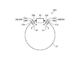
次に、図11を参照して、第3実施形態に係る検出機器20Fについて説明する。なお、第3実施形態では、第1実施形態と同等の構成要素には同じ符号を付し、その詳細な説明を省略する。第3実施形態に係る検出機器20Fは、ループアンテナ21の導体間を接続する点で第1実施形態の検出機器20とは異なる。検出機器20Fは、ループアンテナ21と、導通線部28と、利得低減部としてのスイッチ回路25と、第1作用点としての第1接続点25dと、第2作用点としての第2接続点25eと、RFID検出回路23とを備える。第1及び第2接続点25d、25eは、ループアンテナ21の利得を低減するための作用点として機能するものである。第1接続点25dは、RFID検出回路23の第1回路端子23aからループアンテナ21の第1延在方向に沿ってλ/8離れた位置までのループアンテナ21上の範囲K1内に位置する。第2接続点25eは、RFID検出回路23の第2回路端子23bからループアンテナ21の第2延在方向に沿ってλ/8離れた位置までのループアンテナ21上の範囲K2内に位置する。第1及び第2接続点25d、25eは、導通線部28が接続される。
[Third Embodiment]
Next, a detection device 20F according to a third embodiment will be described with reference to FIG. In addition, in 3rd Embodiment, the same code|symbol is attached|subjected to the component equivalent to 1st Embodiment, and the detailed description is abbreviate|omitted. A detecting device 20F according to the third embodiment differs from the detecting device 20 of the first embodiment in that the conductors of the loop antenna 21 are connected. The detection device 20F includes the loop antenna 21, the conductive line portion 28, the switch circuit 25 as the gain reduction portion, the first connection point 25d as the first point of action, and the second connection point 25e as the second point of action. and an RFID detection circuit 23 . The first and second connection points 25 d and 25 e function as points of action for reducing the gain of the loop antenna 21 . The first connection point 25 d is located within a range K 1 on the loop antenna 21 from the first circuit terminal 23 a of the RFID detection circuit 23 to a position separated by λ/8 along the first extending direction of the loop antenna 21 . The second connection point 25 e is located within a range K 2 on the loop antenna 21 from the second circuit terminal 23 b of the RFID detection circuit 23 to a position separated by λ/8 along the second extending direction of the loop antenna 21 . A conductive line portion 28 is connected to the first and second connection points 25d and 25e.

導通線部28は、ループアンテナ21の導体間を接続するものである。導通線部28は、導電性の部材から形成され、導通線28a、28bを含んで構成される。導通線28aは、一端が第1接続点25dに接続され、他端がスイッチ回路25のスイッチ端子25aに接続されている。導通線28bは、一端が第2接続点25eに接続され、他端がスイッチ回路25のスイッチ端子25bに接続されている。導通線部28は、スイッチ回路25がオンされることで導通し、スイッチ回路25がオフされることで非導通となる。 The conducting wire portion 28 connects the conductors of the loop antenna 21 . The conducting wire portion 28 is made of a conductive member and includes conducting wires 28a and 28b. The conductive line 28 a has one end connected to the first connection point 25 d and the other end connected to the switch terminal 25 a of the switch circuit 25 . The conductive line 28 b has one end connected to the second connection point 25 e and the other end connected to the switch terminal 25 b of the switch circuit 25 . The conduction line portion 28 becomes conductive when the switch circuit 25 is turned on, and becomes non-conductive when the switch circuit 25 is turned off.

スイッチ回路25は、電気的な接続をオン又はオフに切り替えるものである。スイッチ回路25は、導通線28aと導通線28bとの間に設けられ、RFID検出回路23と並列に接続される。スイッチ回路25は、スイッチ端子25aと、スイッチ端子25bと、切替バー25cとを含んで構成される。スイッチ回路25は、スイッチ端子25aが導通線28aの他端に接続され、スイッチ端子25bが導通線28bの他端に接続されている。切替バー25cは、スイッチ端子25a、25bを互いに電気的に接続状態(オン)又は非接続状態(オフ)に切り替える。つまり、切替バー25cは、導通線28aと導通線28bとを通電状態又は非通電状態に切り替える。 The switch circuit 25 switches the electrical connection on or off. The switch circuit 25 is provided between the conductive line 28 a and the conductive line 28 b and connected in parallel with the RFID detection circuit 23 . The switch circuit 25 includes a switch terminal 25a, a switch terminal 25b, and a switching bar 25c. The switch circuit 25 has a switch terminal 25a connected to the other end of the conductive line 28a, and a switch terminal 25b connected to the other end of the conductive line 28b. The switching bar 25c switches the switch terminals 25a and 25b to be electrically connected (ON) or disconnected (OFF). In other words, the switching bar 25c switches the conduction line 28a and the conduction line 28b between the conducting state and the non-conducting state.

検出機器20Fは、例えば、検出対象の状態に応じてスイッチ回路25のスイッチ端子25a、25bを接続状態(オン)することで、導通線28a及び導通線28bを通電状態とし、RFID検出回路23とループアンテナ21とのアンテナ整合を不一致状態とする。言い換えれば、検出機器20Fは、スイッチ回路25をオンし、RFID検出回路23とループアンテナ21とのインピーダンスを不整合にしてループアンテナ21を利得低減状態に切り替える。検出機器20Fは、スイッチ回路25のオン抵抗を相対的に小さくすることで、より好適にインピーダンスを不整合とすることができる。スイッチ回路25のオン抵抗は、例えば1Ω以下が好ましい。検出機器20Fは、検出対象の状態に応じてスイッチ回路25のスイッチ端子2a、2bを非接続状態(オフ)することで、導通線28a及び導通線28bを非通電状態とし、RFID検出回路23とループアンテナ21とのアンテナ整合を一致状態とする。言い換えれば、検出機器20Fは、スイッチ回路25をオフし、RFID検出回路23とループアンテナ21とのインピーダンスを整合させてループアンテナ21を利得非低減状態に切り替える。 For example, the detection device 20F connects (turns on) the switch terminals 25a and 25b of the switch circuit 25 according to the state of the object to be detected, thereby energizing the conduction line 28a and the conduction line 28b. Antenna matching with the loop antenna 21 is set to a non-matching state. In other words, the detection device 20F turns on the switch circuit 25 to make the impedances of the RFID detection circuit 23 and the loop antenna 21 mismatch to switch the loop antenna 21 to the gain reduction state. The detection device 20F can make the impedance mismatch more preferably by making the ON resistance of the switch circuit 25 relatively small. The ON resistance of the switch circuit 25 is preferably 1Ω or less, for example. The detection device 20F disconnects ( turns off) the switch terminals 25a and 25b of the switch circuit 25 in accordance with the state of the object to be detected, thereby deenergizing the conduction lines 28a and 28b. Antenna matching between the detection circuit 23 and the loop antenna 21 is brought into a matching state. In other words, the detection device 20F turns off the switch circuit 25, matches the impedances of the RFID detection circuit 23 and the loop antenna 21, and switches the loop antenna 21 to the gain non-reduction state.

以上のように、第3実施形態の検出機器20Fは、第1接続点25d及び第2接続点25eを互いに電気的に接続状態又は非接続状態に切り替え可能なスイッチ回路25を含んで構成される。スイッチ回路25は、第1接続点25d及び第2接続点25eを非接続状態とした利得非低減状態と、第1接続点25d及び第2接続点25eを接続状態とした利得低減状態と、を切り替え可能である。 As described above, the detection device 20F of the third embodiment includes the switch circuit 25 that can switch the first connection point 25d and the second connection point 25e between the electrically connected state and the non-connected state. . The switch circuit 25 has a gain non-reduction state in which the first connection point 25d and the second connection point 25e are not connected, and a gain reduction state in which the first connection point 25d and the second connection point 25e are connected. Switchable.

この構成により、検出機器20Fは、検出対象の状態に応じてRFID検出回路23とループアンテナ21とのインピーダンスを不整合とすることができる。これにより、検出機器20Fは、利得低減状態を実現することができ、ループアンテナ21を無効化することができる。また、検出機器20Fは、検出対象の状態に応じてRFID検出回路23とループアンテナ21とのインピーダンスを整合させることができる。これにより、検出機器20Fは、利得非低減状態を実現することができ、ループアンテナ21を有効化することができる。この結果、検出機器20Fは、検出対象の検出精度を向上することができる。 With this configuration, the detection device 20F can make the impedances of the RFID detection circuit 23 and the loop antenna 21 mismatch according to the state of the object to be detected. This allows the detection device 20F to achieve a reduced gain state and disable the loop antenna 21 . Further, the detection device 20F can match the impedances of the RFID detection circuit 23 and the loop antenna 21 according to the state of the object to be detected. This allows the detection device 20F to achieve a non-reduced gain state and enable the loop antenna 21 . As a result, the detection device 20F can improve the detection accuracy of the detection target.

〔第3実施形態の変形例〕
次に、図12を参照して、第3実施形態の変形例に係る検出機器20Gについて説明する。検出機器20Gは、ループアンテナ21の代わりにダイポールアンテナ40を備える点で第3実施形態の検出機器20Fとは異なる。検出機器20Gは、ダイポールアンテナ40と、導通線部28と、スイッチ回路25と、第1接続点25dと、第2接続点25eと、RFID検出回路23とを備える。第1及び第2接続点25d、25eは、ダイポールアンテナ40の利得を低減するための作用点として機能するものである。第1接続点25dは、RFID検出回路23の第1回路端子23aからダイポールアンテナ40の第1エレメント41の第1延在方向に沿ってλ/8離れた位置までの第1エレメント41上の範囲K1内に位置する。第2接続点25eは、RFID検出回路23の第2回路端子23bから第2エレメント42の第2延在方向に沿ってλ/8離れた位置までの第2エレメント42上の範囲K2内に位置する。第1及び第2接続点25d、25eは、導通線部28が接続される。
[Modification of the third embodiment]
Next, a detection device 20G according to a modification of the third embodiment will be described with reference to FIG. The detection device 20G differs from the detection device 20F of the third embodiment in that it includes a dipole antenna 40 instead of the loop antenna 21. FIG. The detection device 20G includes a dipole antenna 40, a conducting line portion 28, a switch circuit 25, a first connection point 25d, a second connection point 25e, and an RFID detection circuit 23. The first and second connection points 25 d and 25 e function as points of action for reducing the gain of the dipole antenna 40 . The first connection point 25d is a range on the first element 41 from the first circuit terminal 23a of the RFID detection circuit 23 to a position separated by λ/8 along the first extending direction of the first element 41 of the dipole antenna 40. Located within K1. The second connection point 25e is located within a range K2 on the second element 42 from the second circuit terminal 23b of the RFID detection circuit 23 to a position separated by λ/8 along the second extending direction of the second element 42. do. A conductive line portion 28 is connected to the first and second connection points 25d and 25e.

導通線部28は、ダイポールアンテナ40の導体間を接続するものである。導通線部28の導通線28aは、一端が第1接続点25dに接続され、他端がスイッチ回路25のスイッチ端子25aに接続されている。導通線28bは、一端が第2接続点25eに接続され、他端がスイッチ回路25のスイッチ端子25bに接続されている。導通線部28は、スイッチ回路25がオンされることで導通し、スイッチ回路25がオフされることで非導通となる。 The conducting wire portion 28 connects the conductors of the dipole antenna 40 . A conducting wire 28 a of the conducting wire portion 28 has one end connected to the first connection point 25 d and the other end connected to the switch terminal 25 a of the switch circuit 25 . The conductive line 28 b has one end connected to the second connection point 25 e and the other end connected to the switch terminal 25 b of the switch circuit 25 . The conduction line portion 28 becomes conductive when the switch circuit 25 is turned on, and becomes non-conductive when the switch circuit 25 is turned off.

検出機器20Gは、例えば、検出対象の状態に応じてスイッチ回路25のスイッチ端子25a、25bを接続状態(オン)することで、導通線28a及び導通線28bを通電状態とし、ダイポールアンテナ40の利得を低減する利得低減状態に切り替える。また、検出機器20Gは、検出対象の状態に応じてスイッチ回路25のスイッチ端子2a、2bを非接続状態(オフ)することで、導通線28a及び導通線28bを非通電状態とし、ダイポールアンテナ40の利得を低減しない利得非低減状態に切り替える。 The detection device 20G, for example, connects (turns on) the switch terminals 25a and 25b of the switch circuit 25 according to the state of the object to be detected, thereby energizing the conductive lines 28a and 28b, and increasing the gain of the dipole antenna 40. switch to a gain reduction state that reduces In addition, the detection device 20G puts the conduction lines 28a and 28b into a non - conducting state by disconnecting (turning off) the switch terminals 25a and 25b of the switch circuit 25 according to the state of the object to be detected. , to a non-gain reduction state in which the gain of the dipole antenna 40 is not reduced.

以上のように、第3実施形態の変形例に係る検出機器20Gは、検出対象の状態に応じてRFID検出回路23とダイポールアンテナ40とのインピーダンスを不整合とすることができる。これにより、検出機器20Gは、利得低減状態を実現することができ、ダイポールアンテナ40を無効化することができる。また、検出機器20Gは、検出対象の状態に応じてRFID検出回路23とダイポールアンテナ40とのインピーダンスを整合させることができる。これにより、検出機器20Gは、利得非低減状態を実現することができ、ダイポールアンテナ40を有効化することができる。この結果、検出機器20Gは、検出対象の検出精度を向上することができる。 As described above, the detection device 20G according to the modified example of the third embodiment can make the impedances of the RFID detection circuit 23 and the dipole antenna 40 mismatch according to the state of the detection target. This allows the detection device 20G to achieve a reduced gain state and disable the dipole antenna 40 . Further, the detection device 20G can match the impedances of the RFID detection circuit 23 and the dipole antenna 40 according to the state of the object to be detected. This allows the detection device 20G to achieve a non-reduced gain state and enable the dipole antenna 40 . As a result, the detection device 20G can improve the detection accuracy of the detection target.

なお、各検出機器20~20Gのアンテナは、ループアンテナ21又はダイポールアンテナ40である例について説明したが、これに限定されず、モノポールアンテナ等のアンテナであってもよい。 Although an example in which the antennas of the detection devices 20 to 20G are the loop antenna 21 or the dipole antenna 40 has been described, the antenna is not limited to this, and may be an antenna such as a monopole antenna.

また、検出システム1は、各検出機器20が座席2aの座面部2bに設けられ、搭乗者の着座を判定する例について説明したが、これに限定されない。例えば、検出システム1は、各検出機器20がシートベルトのバックル(図示省略)に設けられ、搭乗者によるシートベルトの締結を判定してもよい。この場合、第1及び第2スイッチ回路22R、22Lは、例えば、シートベルトのタングプレートがバックルに装着されていない場合にオフし、ループアンテナ21を利得低減状態としてRFID検出回路23を起動しない。また、第1及び第2スイッチ回路22R、22Lは、タングプレートがバックルに装着された場合にオンし、ループアンテナ21を利得非低減状態としてRFID検出回路23を起動させる。 Moreover, although the detection system 1 has been described as an example in which each detection device 20 is provided on the seat surface portion 2b of the seat 2a to determine whether or not the passenger is seated, the detection system 1 is not limited to this. For example, in the detection system 1, each detection device 20 may be provided in a seat belt buckle (not shown) to determine whether the passenger has fastened the seat belt. In this case, the first and second switch circuits 22R and 22L are turned off, for example, when the tongue plate of the seat belt is not attached to the buckle, and the loop antenna 21 is in the gain reduction state and the RFID detection circuit 23 is not activated. Also, the first and second switch circuits 22R and 22L are turned on when the tongue plate is attached to the buckle, and activate the RFID detection circuit 23 by setting the loop antenna 21 to the non-gain reduction state.

また、各検出機器20は、車両2に搭載する例について説明したが、これに限定されず、例えば、船舶や航空機、建築物等に搭載してもよい。 In addition, although an example in which each detection device 20 is mounted on the vehicle 2 has been described, the detection device 20 is not limited to this, and may be mounted on, for example, a ship, an aircraft, a building, or the like.

また、検出機器20Cは、電線26A、26B(同軸ケーブル27A、27B)を介して第1及び第2スイッチ回路22R、22Lをダイポールアンテナ40に接続してもよい。検出機器20Dは、電線26A、26B(同軸ケーブル27A、27B)を介して第1及び第2コンデンサ回路24R、24Lをループアンテナ21に接続してもよい。検出機器20Eは、電線26A、26B(同軸ケーブル27A、27B)を介して第1及び第2コンデンサ回路24R、24Lをダイポールアンテナ40に接続してもよい。検出機器20Fは、電線26A(同軸ケーブル27A)を介してスイッチ回路25をループアンテナ21に接続してもよい。検出機器20Gは、電線26A(同軸ケーブル27A)を介してスイッチ回路25をダイポールアンテナ40に接続してもよい。 Further, the detection device 20C may connect the first and second switch circuits 22R and 22L to the dipole antenna 40 via electric wires 26A and 26B (coaxial cables 27A and 27B). The detection device 20D may connect the first and second capacitor circuits 24R, 24L to the loop antenna 21 via electric wires 26A, 26B (coaxial cables 27A, 27B). The detection device 20E may connect the first and second capacitor circuits 24R, 24L to the dipole antenna 40 via wires 26A, 26B (coaxial cables 27A, 27B). The detection device 20F may connect the switch circuit 25 to the loop antenna 21 via the electric wire 26A (coaxial cable 27A). The detection device 20G may connect the switch circuit 25 to the dipole antenna 40 via the electric wire 26A (coaxial cable 27A).

1 検出システム
10 RFIDリーダー(読み取り装置)
20、20A、20B、20C、20D、20E、20F、20G 検出機器
21 ループアンテナ(アンテナ)
22 スイッチ部(利得低減部)
22R 第1スイッチ回路
22L 第2スイッチ回路
22a、22b スイッチ端子(第1作用点、第1端子、第2端子)
22d、22e スイッチ端子(第2作用点、第3端子、第4端子)
23 RFID検出回路(信号出力部)
23a 第1回路端子
23b 第2回路端子
24 コンデンサ部(利得低減部)
24R 第1コンデンサ回路
24L 第2コンデンサ回路
24a、24b 平板(第1作用点、第1平板、第2平板)
24c、24d 平板(第2作用点、第3平板、第4平板)
25d 第1接続点
25e 第2接続点
25 スイッチ回路(第3スイッチ回路、利得低減部)
30 ECU(判定部)
40 ダイポールアンテナ
K1、K2 範囲
1 detection system 10 RFID reader (reading device)
20, 20A, 20B, 20C, 20D, 20E, 20F, 20G Detection device 21 Loop antenna (antenna)
22 switch unit (gain reduction unit)
22R first switch circuit 22L second switch circuits 22a, 22b switch terminals (first action point, first terminal, second terminal)
22d, 22e switch terminals (second point of action, third terminal, fourth terminal)
23 RFID detection circuit (signal output unit)
23a first circuit terminal 23b second circuit terminal 24 capacitor section (gain reduction section)
24R First capacitor circuit 24L Second capacitor circuits 24a, 24b Plate (first point of action, first plate, second plate)
24c, 24d flat plate (second point of action, third flat plate, fourth flat plate)
25d First connection point 25e Second connection point 25 Switch circuit (third switch circuit, gain reduction unit)
30 ECU (judgment unit)
40 dipole antennas K1, K2 range

Claims (6)

信号を含む電波を送受信するアンテナと、
前記アンテナに接続される第1回路端子及び第2回路端子を含んで構成され前記アンテナにより受信した信号に含まれる電力供給用の信号を動力として起動し検出対象を検出したことを表す検出信号を前記アンテナに出力する信号出力部と、
前記検出対象を検出していない場合に前記アンテナの利得を低減し前記信号出力部を起動させない利得低減状態となり、前記検出対象を検出した場合に前記アンテナの利得を低減せずに前記信号出力部を起動させ当該信号出力部から前記検出信号を出力させる利得非低減状態となる利得低減部と、を備え、
前記利得低減部は、前記電波の波長をλとしたとき、前記第1回路端子から前記アンテナの第1延在方向に沿ってλ/8離れた位置までの前記アンテナ上の範囲内に前記アンテナの利得を低減するための第1作用点を有し、且つ、前記第2回路端子から前記アンテナの第2延在方向に沿ってλ/8離れた位置までの前記アンテナ上の範囲内に前記アンテナの利得を低減するための第2作用点を有することを特徴とする検出機器。
An antenna for transmitting and receiving radio waves containing signals;
It comprises a first circuit terminal and a second circuit terminal connected to the antenna, and is powered by a power supply signal included in the signal received by the antenna, and generates a detection signal indicating detection of a detection target. a signal output unit that outputs to the antenna;
When the detection target is not detected, the gain of the antenna is reduced to enter a gain reduction state in which the signal output unit is not activated, and when the detection target is detected, the signal output unit does not reduce the gain of the antenna. and a gain reduction unit in a gain non-reduction state that activates and outputs the detection signal from the signal output unit ,
The gain reduction section is provided within a range on the antenna from the first circuit terminal to a position separated by λ/8 along the first extending direction of the antenna, where λ is the wavelength of the radio wave. and within a range on the antenna from the second circuit terminal to a position separated by λ/8 along the second extending direction of the antenna A detection device, characterized in that it has a second point of action for reducing the gain of the antenna.
前記第1及び第2作用点は、前記信号出力部と前記アンテナとを通電状態又は非通電状態にするための作用点である請求項1に記載の検出機器。 2. The detecting device according to claim 1, wherein said first and second points of action are points of action for bringing said signal output section and said antenna into an energized state or a non-energized state. 前記利得低減部は、前記第1作用点としての第1端子及び第2端子を互いに電気的に接続状態又は非接続状態に切り替え可能な第1スイッチ回路と、前記第2作用点としての第3端子及び第4端子を互いに電気的に接続状態又は非接続状態に切り替え可能な第2スイッチ回路と、を含んで構成され、
前記第1端子及び前記第2端子を接続状態とし、且つ、前記第3端子及び前記第4端子を接続状態とした前記利得非低減状態と、前記第1端子及び前記第2端子を非接続状態とし、且つ、前記第3端子及び前記第4端子を非接続状態とした前記利得低減状態と、を切り替え可能である請求項1又は2に記載の検出機器。
The gain reduction section includes a first switching circuit capable of switching electrically connected or disconnected states between a first terminal and a second terminal as the first point of action, and a third switching circuit as the second point of action. a second switch circuit capable of switching the terminal and the fourth terminal to an electrically connected state or a non-connected state;
the gain non-reduction state in which the first terminal and the second terminal are in a connected state and the third terminal and the fourth terminal are in a connected state; and the first terminal and the second terminal are in a non-connected state. and the gain reduction state in which the third terminal and the fourth terminal are in a non-connected state.
前記利得低減部は、前記第1作用点としての第1平板及び第2平板を蓄電可能状態又は蓄電不可状態に切り替え可能な第1コンデンサ回路と、前記第2作用点としての第3平板及び第4平板を蓄電可能状態又は蓄電不可状態に切り替え可能な第2コンデンサ回路と、を含んで構成され、
前記第1平板及び前記第2平板を蓄電可能状態とし、且つ、前記第3平板及び前記第4平板を蓄電可能状態とした前記利得非低減状態と、前記第1平板及び前記第2平板を蓄電不可状態とし、且つ、前記第3平板及び前記第4平板を蓄電不可状態とした前記利得低減状態と、を切り替え可能である請求項1又は2に記載の検出機器。
The gain reduction section includes a first capacitor circuit capable of switching the first plate and the second plate as the first point of action between a chargeable state and a chargeable state, and a third plate and the second plate as the second point of action. and a second capacitor circuit capable of switching the 4 flat plates to a chargeable state or a chargeable state,
The gain non-reducing state in which the first plate and the second plate are in a chargeable state and the third plate and the fourth plate are in a chargeable state, and the first plate and the second plate are in a chargeable state. 3. The detecting device according to claim 1, wherein switching between the gain reduction state in which the third plate and the fourth plate are in the non-storage state and the gain reduction state is switchable.
前記利得低減部は、前記第1作用点及び前記第2作用点を互いに電気的に接続状態又は非接続状態に切り替え可能な第3スイッチ回路を含んで構成され、
前記第3スイッチ回路は、前記第1作用点及び前記第2作用点を非接続状態とした前記利得非低減状態と、前記第1作用点及び前記第2作用点を接続状態とした前記利得低減状態と、を切り替え可能である請求項1に記載の検出機器。
the gain reduction unit includes a third switch circuit capable of switching the first point of action and the second point of action between an electrically connected state or a non-connected state;
The third switch circuit has the gain non-reducing state in which the first point of action and the second point of action are in a non-connected state, and the gain reduction state in which the first point of action and the second point of action are in a connected state. 2. The detection device of claim 1, wherein the detection device is switchable between a state and a state.
信号を含む電波を送受信し、少なくとも電力供給用の信号を含む送信信号を送信する読み取り装置と、
前記読み取り装置との間で相互に信号を送受信するアンテナ、前記アンテナに接続される第1回路端子及び第2回路端子を有し前記アンテナにより受信した信号に含まれる電力供給用の信号を動力として起動し検出対象を検出したことを表す検出信号を前記アンテナに出力する信号出力部、及び、前記検出対象を検出していない場合に前記アンテナの利得を低減し前記信号出力部を起動させない利得低減状態となり、前記検出対象を検出した場合に前記アンテナの利得を低減せずに前記信号出力部を起動させ当該信号出力部から前記検出信号を出力させる利得非低減状態となる利得低減部を含んで構成される検出機器と、
前記読み取り装置に接続され、当該読み取り装置が受信した前記検出信号に基づいて前記検出対象の状態を判定する判定部と、を備え、
前記利得低減部は、前記電波の波長をλとしたとき、前記第1回路端子から前記アンテナの第1延在方向に沿ってλ/8離れた位置までの前記アンテナ上の範囲内に前記アンテナの利得を低減するための第1作用点を有し、且つ、前記第2回路端子から前記アンテナの第2延在方向に沿ってλ/8離れた位置までの前記アンテナ上の範囲内に前記アンテナの利得を低減するための第2作用点を有することを特徴とする検出システム。
a reading device that transmits and receives radio waves containing a signal and transmits a transmission signal containing at least a signal for power supply;
An antenna for mutually transmitting and receiving signals to and from the reading device, a first circuit terminal and a second circuit terminal connected to the antenna, and powered by a power supply signal included in the signal received by the antenna. A signal output unit that is activated and outputs a detection signal indicating that a detection target has been detected to the antenna, and a gain reduction that reduces the gain of the antenna and does not activate the signal output unit when the detection target is not detected. and a gain reduction unit that enters a gain non-reduction state in which, when the detection target is detected, the signal output unit is activated without reducing the gain of the antenna and the detection signal is output from the signal output unit . a detection device comprising:
a determination unit that is connected to the reading device and determines the state of the detection target based on the detection signal received by the reading device;
The gain reduction section is provided within a range on the antenna from the first circuit terminal to a position separated by λ/8 along the first extending direction of the antenna, where λ is the wavelength of the radio wave. and within a range on the antenna from the second circuit terminal to a position separated by λ/8 along the second extending direction of the antenna A detection system, characterized in that it has a second point of action for reducing the gain of the antenna.
JP2018101233A 2018-05-28 2018-05-28 Detection equipment and detection system Active JP7152190B2 (en)

Priority Applications (4)

Application Number Priority Date Filing Date Title
JP2018101233A JP7152190B2 (en) 2018-05-28 2018-05-28 Detection equipment and detection system
EP19175093.4A EP3576220B1 (en) 2018-05-28 2019-05-17 Detection device and detection system
US16/416,551 US10733398B2 (en) 2018-05-28 2019-05-20 Detection device and detection system
CN201910446828.2A CN110539719B (en) 2018-05-28 2019-05-27 Detection device and detection system

Applications Claiming Priority (1)

Application Number Priority Date Filing Date Title
JP2018101233A JP7152190B2 (en) 2018-05-28 2018-05-28 Detection equipment and detection system

Publications (2)

Publication Number Publication Date
JP2019206201A JP2019206201A (en) 2019-12-05
JP7152190B2 true JP7152190B2 (en) 2022-10-12

Family

ID=66589434

Family Applications (1)

Application Number Title Priority Date Filing Date
JP2018101233A Active JP7152190B2 (en) 2018-05-28 2018-05-28 Detection equipment and detection system

Country Status (4)

Country Link
US (1) US10733398B2 (en)
EP (1) EP3576220B1 (en)
JP (1) JP7152190B2 (en)
CN (1) CN110539719B (en)

Families Citing this family (1)

* Cited by examiner, † Cited by third party
Publication number Priority date Publication date Assignee Title
JP6734831B2 (en) * 2017-10-04 2020-08-05 矢崎総業株式会社 Detection equipment and detection system

Citations (10)

* Cited by examiner, † Cited by third party
Publication number Priority date Publication date Assignee Title
JP2006217048A (en) 2005-02-01 2006-08-17 Matsushita Electric Ind Co Ltd Reader apparatus for contactless communication
JP2008545137A (en) 2005-06-29 2008-12-11 ソシエテ ドゥ テクノロジー ミシュラン RFID to store SAW calibration factor
JP2011091541A (en) 2009-10-21 2011-05-06 Takaya Corp Antenna device, and communication system
US20110279232A1 (en) 2008-06-03 2011-11-17 Keystone Technology Solutions, Llc Systems and methods to selectively connect antennas to receive and backscatter radio frequency signals
JP2013055611A (en) 2011-09-06 2013-03-21 Renesas Electronics Corp Radio communication system, radio communication method and data transmission device
JP5700135B2 (en) 2011-10-28 2015-04-15 株式会社村田製作所 Power receiving device, power transmitting device, and wireless power transmission system
JP2015529971A (en) 2012-07-24 2015-10-08 レイセオン カンパニー Capacitor switchable with switch
JP2016127442A (en) 2015-01-05 2016-07-11 株式会社リコー Radio communication device and mobile terminal device
WO2017043482A1 (en) 2015-09-11 2017-03-16 タカヤ株式会社 Rfid system
JP2017216707A (en) 2017-07-13 2017-12-07 インテル コーポレイション Near-field communication (nfc) and proximity sensor for portable device

Family Cites Families (10)

* Cited by examiner, † Cited by third party
Publication number Priority date Publication date Assignee Title
EP0708002B1 (en) * 1994-10-17 1999-08-11 I.E.E. International Electronics &amp; Engineering S.à.r.l. Method and device for detecting certain parameters of an auxiliary child seat intended to be used to control the functioning of a vehicle air bag
US6476708B1 (en) * 1998-03-20 2002-11-05 Hid Corporation Detection of an RFID device by an RF reader unit operating in a reduced power state
US6940460B2 (en) * 2000-08-28 2005-09-06 In4Tel Ltd. Apparatus and method for enhancing low-frequency operation of mobile communication antennas
US6830193B2 (en) * 2001-11-29 2004-12-14 Matsushita Electric Industrial Co., Ltd. Non-contact IC card
KR100963041B1 (en) * 2008-03-05 2010-06-10 한국전자통신연구원 Apparatus for rfid tag by recognition distance regulation and method for rfid information operation in using the apparatus
CN102301527B (en) * 2008-11-28 2015-06-24 日立化成工业株式会社 Multibeam Antenna Device
JP2013049290A (en) 2010-03-11 2013-03-14 Autoliv Development Ab Seat belt fastening state detection device
WO2011132190A2 (en) * 2010-04-22 2011-10-27 R.F Keeper Ltd Event driven context switching in passive radio frequency identification tags
US8665026B2 (en) * 2012-03-14 2014-03-04 Broadcom Corporation Gain control system
JP5846497B2 (en) 2012-05-23 2016-01-20 アルプス電気株式会社 Vehicle with seat belt

Patent Citations (10)

* Cited by examiner, † Cited by third party
Publication number Priority date Publication date Assignee Title
JP2006217048A (en) 2005-02-01 2006-08-17 Matsushita Electric Ind Co Ltd Reader apparatus for contactless communication
JP2008545137A (en) 2005-06-29 2008-12-11 ソシエテ ドゥ テクノロジー ミシュラン RFID to store SAW calibration factor
US20110279232A1 (en) 2008-06-03 2011-11-17 Keystone Technology Solutions, Llc Systems and methods to selectively connect antennas to receive and backscatter radio frequency signals
JP2011091541A (en) 2009-10-21 2011-05-06 Takaya Corp Antenna device, and communication system
JP2013055611A (en) 2011-09-06 2013-03-21 Renesas Electronics Corp Radio communication system, radio communication method and data transmission device
JP5700135B2 (en) 2011-10-28 2015-04-15 株式会社村田製作所 Power receiving device, power transmitting device, and wireless power transmission system
JP2015529971A (en) 2012-07-24 2015-10-08 レイセオン カンパニー Capacitor switchable with switch
JP2016127442A (en) 2015-01-05 2016-07-11 株式会社リコー Radio communication device and mobile terminal device
WO2017043482A1 (en) 2015-09-11 2017-03-16 タカヤ株式会社 Rfid system
JP2017216707A (en) 2017-07-13 2017-12-07 インテル コーポレイション Near-field communication (nfc) and proximity sensor for portable device

Also Published As

Publication number Publication date
EP3576220B1 (en) 2020-11-18
EP3576220A1 (en) 2019-12-04
CN110539719B (en) 2022-02-11
US10733398B2 (en) 2020-08-04
JP2019206201A (en) 2019-12-05
CN110539719A (en) 2019-12-06
US20190362112A1 (en) 2019-11-28

Similar Documents

Publication Publication Date Title
US10777875B2 (en) Detection device and detection system
CN108944579B (en) Vehicle detection system
US7019620B2 (en) Device for the inductive transmission of electrical power
US9755460B2 (en) Power reception device, power transmission device and wireless power transmission system
US9520916B2 (en) Vehicular power line communication system and transmitter
EP3055701B1 (en) Self-contained branch circuit monitor
US20180138966A1 (en) Vehicle-mounted communication apparatus
US20040113490A1 (en) Data transmission between a chassis and a seat movably arranged on the chassis
KR20150072137A (en) Wireless power charging System of vehicles
JP7152190B2 (en) Detection equipment and detection system
CN104081580A (en) Antenna device and method of antenna configuration
US4761826A (en) Signal separating device
JP6226718B2 (en) Wireless power supply system
JP6451577B2 (en) Wireless communication device
JP5318726B2 (en) Antenna device and communication system
US10403985B2 (en) Wire harness
CN112368947B (en) Device for a vehicle for contactless data transmission
WO2006004184A1 (en) Wireless communication system
KR101204711B1 (en) Landmine detection system with reconfigurable coil structure for noise cancellation
CN109698401B (en) Antenna for low frequency communication in a vehicle environment and low frequency communication system
JP2017139899A (en) Non-contact transmission device, non-contact power reception device and non-contact power transmission system
WO2020095234A1 (en) A bi-functional receiving/ transmitting element for wireless charging
CN114365353A (en) Antenna device, integrated communication device, and wireless communication device
JP2019062373A (en) Composite antenna device

Legal Events

Date Code Title Description
A621 Written request for application examination

Free format text: JAPANESE INTERMEDIATE CODE: A621

Effective date: 20210416

A131 Notification of reasons for refusal

Free format text: JAPANESE INTERMEDIATE CODE: A131

Effective date: 20220628

A521 Request for written amendment filed

Free format text: JAPANESE INTERMEDIATE CODE: A523

Effective date: 20220808

TRDD Decision of grant or rejection written
A01 Written decision to grant a patent or to grant a registration (utility model)

Free format text: JAPANESE INTERMEDIATE CODE: A01

Effective date: 20220927

A61 First payment of annual fees (during grant procedure)

Free format text: JAPANESE INTERMEDIATE CODE: A61

Effective date: 20220929

R150 Certificate of patent or registration of utility model

Ref document number: 7152190

Country of ref document: JP

Free format text: JAPANESE INTERMEDIATE CODE: R150

S531 Written request for registration of change of domicile

Free format text: JAPANESE INTERMEDIATE CODE: R313531

R350 Written notification of registration of transfer

Free format text: JAPANESE INTERMEDIATE CODE: R350