JP7002855B2 - Display device - Google Patents
Display device Download PDFInfo
- Publication number
- JP7002855B2 JP7002855B2 JP2017075519A JP2017075519A JP7002855B2 JP 7002855 B2 JP7002855 B2 JP 7002855B2 JP 2017075519 A JP2017075519 A JP 2017075519A JP 2017075519 A JP2017075519 A JP 2017075519A JP 7002855 B2 JP7002855 B2 JP 7002855B2
- Authority
- JP
- Japan
- Prior art keywords
- film
- sealing film
- pixel array
- organic
- bent portion
- Prior art date
- Legal status (The legal status is an assumption and is not a legal conclusion. Google has not performed a legal analysis and makes no representation as to the accuracy of the status listed.)
- Active
Links
- 238000007789 sealing Methods 0.000 claims description 62
- 230000002093 peripheral effect Effects 0.000 claims description 48
- 230000001681 protective effect Effects 0.000 claims description 19
- 238000007689 inspection Methods 0.000 claims description 5
- 239000011159 matrix material Substances 0.000 claims description 5
- XLYOFNOQVPJJNP-UHFFFAOYSA-N water Substances O XLYOFNOQVPJJNP-UHFFFAOYSA-N 0.000 claims description 4
- 230000007274 generation of a signal involved in cell-cell signaling Effects 0.000 claims description 3
- 239000003086 colorant Substances 0.000 claims description 2
- 239000010408 film Substances 0.000 description 170
- 239000010410 layer Substances 0.000 description 51
- 239000004065 semiconductor Substances 0.000 description 35
- 239000000758 substrate Substances 0.000 description 29
- 230000003014 reinforcing effect Effects 0.000 description 12
- 239000000463 material Substances 0.000 description 10
- 239000012790 adhesive layer Substances 0.000 description 9
- 238000005452 bending Methods 0.000 description 9
- 125000006850 spacer group Chemical group 0.000 description 9
- 238000010586 diagram Methods 0.000 description 5
- 238000010030 laminating Methods 0.000 description 5
- -1 polyethylene terephthalate Polymers 0.000 description 5
- 238000009792 diffusion process Methods 0.000 description 4
- 150000004767 nitrides Chemical class 0.000 description 4
- 229920001721 polyimide Polymers 0.000 description 4
- 229910010271 silicon carbide Inorganic materials 0.000 description 4
- 239000004642 Polyimide Substances 0.000 description 3
- 238000009413 insulation Methods 0.000 description 3
- 239000011347 resin Substances 0.000 description 3
- 229920005989 resin Polymers 0.000 description 3
- 229910052814 silicon oxide Inorganic materials 0.000 description 3
- IJGRMHOSHXDMSA-UHFFFAOYSA-N Atomic nitrogen Chemical compound N#N IJGRMHOSHXDMSA-UHFFFAOYSA-N 0.000 description 2
- VYPSYNLAJGMNEJ-UHFFFAOYSA-N Silicium dioxide Chemical compound O=[Si]=O VYPSYNLAJGMNEJ-UHFFFAOYSA-N 0.000 description 2
- XUIMIQQOPSSXEZ-UHFFFAOYSA-N Silicon Chemical compound [Si] XUIMIQQOPSSXEZ-UHFFFAOYSA-N 0.000 description 2
- AMGQUBHHOARCQH-UHFFFAOYSA-N indium;oxotin Chemical compound [In].[Sn]=O AMGQUBHHOARCQH-UHFFFAOYSA-N 0.000 description 2
- 238000002347 injection Methods 0.000 description 2
- 239000007924 injection Substances 0.000 description 2
- 239000011810 insulating material Substances 0.000 description 2
- 238000000034 method Methods 0.000 description 2
- 229920000139 polyethylene terephthalate Polymers 0.000 description 2
- 239000005020 polyethylene terephthalate Substances 0.000 description 2
- 229910052710 silicon Inorganic materials 0.000 description 2
- 239000010703 silicon Substances 0.000 description 2
- HBMJWWWQQXIZIP-UHFFFAOYSA-N silicon carbide Chemical compound [Si+]#[C-] HBMJWWWQQXIZIP-UHFFFAOYSA-N 0.000 description 2
- 229920000178 Acrylic resin Polymers 0.000 description 1
- 239000004925 Acrylic resin Substances 0.000 description 1
- OKTJSMMVPCPJKN-UHFFFAOYSA-N Carbon Chemical compound [C] OKTJSMMVPCPJKN-UHFFFAOYSA-N 0.000 description 1
- 239000004593 Epoxy Substances 0.000 description 1
- 239000004743 Polypropylene Substances 0.000 description 1
- 229910052581 Si3N4 Inorganic materials 0.000 description 1
- 239000002253 acid Substances 0.000 description 1
- NIXOWILDQLNWCW-UHFFFAOYSA-N acrylic acid group Chemical group C(C=C)(=O)O NIXOWILDQLNWCW-UHFFFAOYSA-N 0.000 description 1
- 230000001154 acute effect Effects 0.000 description 1
- QVGXLLKOCUKJST-UHFFFAOYSA-N atomic oxygen Chemical compound [O] QVGXLLKOCUKJST-UHFFFAOYSA-N 0.000 description 1
- 229910052799 carbon Inorganic materials 0.000 description 1
- 150000001875 compounds Chemical class 0.000 description 1
- 239000004020 conductor Substances 0.000 description 1
- KPUWHANPEXNPJT-UHFFFAOYSA-N disiloxane Chemical class [SiH3]O[SiH3] KPUWHANPEXNPJT-UHFFFAOYSA-N 0.000 description 1
- 238000005401 electroluminescence Methods 0.000 description 1
- 239000011521 glass Substances 0.000 description 1
- 230000005525 hole transport Effects 0.000 description 1
- 238000004519 manufacturing process Methods 0.000 description 1
- 239000012528 membrane Substances 0.000 description 1
- 229910052757 nitrogen Inorganic materials 0.000 description 1
- 239000011368 organic material Substances 0.000 description 1
- 229910052760 oxygen Inorganic materials 0.000 description 1
- 239000001301 oxygen Substances 0.000 description 1
- 230000000149 penetrating effect Effects 0.000 description 1
- 229920001155 polypropylene Polymers 0.000 description 1
- HQVNEWCFYHHQES-UHFFFAOYSA-N silicon nitride Chemical compound N12[Si]34N5[Si]62N3[Si]51N64 HQVNEWCFYHHQES-UHFFFAOYSA-N 0.000 description 1
- 239000010409 thin film Substances 0.000 description 1
- YVTHLONGBIQYBO-UHFFFAOYSA-N zinc indium(3+) oxygen(2-) Chemical compound [O--].[Zn++].[In+3] YVTHLONGBIQYBO-UHFFFAOYSA-N 0.000 description 1
Images


Classifications
-
- G—PHYSICS
- G09—EDUCATION; CRYPTOGRAPHY; DISPLAY; ADVERTISING; SEALS
- G09G—ARRANGEMENTS OR CIRCUITS FOR CONTROL OF INDICATING DEVICES USING STATIC MEANS TO PRESENT VARIABLE INFORMATION
- G09G3/00—Control arrangements or circuits, of interest only in connection with visual indicators other than cathode-ray tubes
- G09G3/006—Electronic inspection or testing of displays and display drivers, e.g. of LED or LCD displays
-
- G—PHYSICS
- G09—EDUCATION; CRYPTOGRAPHY; DISPLAY; ADVERTISING; SEALS
- G09G—ARRANGEMENTS OR CIRCUITS FOR CONTROL OF INDICATING DEVICES USING STATIC MEANS TO PRESENT VARIABLE INFORMATION
- G09G3/00—Control arrangements or circuits, of interest only in connection with visual indicators other than cathode-ray tubes
- G09G3/20—Control arrangements or circuits, of interest only in connection with visual indicators other than cathode-ray tubes for presentation of an assembly of a number of characters, e.g. a page, by composing the assembly by combination of individual elements arranged in a matrix no fixed position being assigned to or needed to be assigned to the individual characters or partial characters
- G09G3/22—Control arrangements or circuits, of interest only in connection with visual indicators other than cathode-ray tubes for presentation of an assembly of a number of characters, e.g. a page, by composing the assembly by combination of individual elements arranged in a matrix no fixed position being assigned to or needed to be assigned to the individual characters or partial characters using controlled light sources
- G09G3/30—Control arrangements or circuits, of interest only in connection with visual indicators other than cathode-ray tubes for presentation of an assembly of a number of characters, e.g. a page, by composing the assembly by combination of individual elements arranged in a matrix no fixed position being assigned to or needed to be assigned to the individual characters or partial characters using controlled light sources using electroluminescent panels
- G09G3/32—Control arrangements or circuits, of interest only in connection with visual indicators other than cathode-ray tubes for presentation of an assembly of a number of characters, e.g. a page, by composing the assembly by combination of individual elements arranged in a matrix no fixed position being assigned to or needed to be assigned to the individual characters or partial characters using controlled light sources using electroluminescent panels semiconductive, e.g. using light-emitting diodes [LED]
- G09G3/3208—Control arrangements or circuits, of interest only in connection with visual indicators other than cathode-ray tubes for presentation of an assembly of a number of characters, e.g. a page, by composing the assembly by combination of individual elements arranged in a matrix no fixed position being assigned to or needed to be assigned to the individual characters or partial characters using controlled light sources using electroluminescent panels semiconductive, e.g. using light-emitting diodes [LED] organic, e.g. using organic light-emitting diodes [OLED]
- G09G3/3225—Control arrangements or circuits, of interest only in connection with visual indicators other than cathode-ray tubes for presentation of an assembly of a number of characters, e.g. a page, by composing the assembly by combination of individual elements arranged in a matrix no fixed position being assigned to or needed to be assigned to the individual characters or partial characters using controlled light sources using electroluminescent panels semiconductive, e.g. using light-emitting diodes [LED] organic, e.g. using organic light-emitting diodes [OLED] using an active matrix
- G09G3/3233—Control arrangements or circuits, of interest only in connection with visual indicators other than cathode-ray tubes for presentation of an assembly of a number of characters, e.g. a page, by composing the assembly by combination of individual elements arranged in a matrix no fixed position being assigned to or needed to be assigned to the individual characters or partial characters using controlled light sources using electroluminescent panels semiconductive, e.g. using light-emitting diodes [LED] organic, e.g. using organic light-emitting diodes [OLED] using an active matrix with pixel circuitry controlling the current through the light-emitting element
-
- H—ELECTRICITY
- H10—SEMICONDUCTOR DEVICES; ELECTRIC SOLID-STATE DEVICES NOT OTHERWISE PROVIDED FOR
- H10K—ORGANIC ELECTRIC SOLID-STATE DEVICES
- H10K50/00—Organic light-emitting devices
- H10K50/80—Constructional details
- H10K50/84—Passivation; Containers; Encapsulations
- H10K50/844—Encapsulations
-
- H—ELECTRICITY
- H10—SEMICONDUCTOR DEVICES; ELECTRIC SOLID-STATE DEVICES NOT OTHERWISE PROVIDED FOR
- H10K—ORGANIC ELECTRIC SOLID-STATE DEVICES
- H10K59/00—Integrated devices, or assemblies of multiple devices, comprising at least one organic light-emitting element covered by group H10K50/00
- H10K59/10—OLED displays
- H10K59/12—Active-matrix OLED [AMOLED] displays
- H10K59/131—Interconnections, e.g. wiring lines or terminals
-
- H—ELECTRICITY
- H10—SEMICONDUCTOR DEVICES; ELECTRIC SOLID-STATE DEVICES NOT OTHERWISE PROVIDED FOR
- H10K—ORGANIC ELECTRIC SOLID-STATE DEVICES
- H10K59/00—Integrated devices, or assemblies of multiple devices, comprising at least one organic light-emitting element covered by group H10K50/00
- H10K59/80—Constructional details
- H10K59/87—Passivation; Containers; Encapsulations
- H10K59/873—Encapsulations
- H10K59/8731—Encapsulations multilayered coatings having a repetitive structure, e.g. having multiple organic-inorganic bilayers
-
- H—ELECTRICITY
- H10—SEMICONDUCTOR DEVICES; ELECTRIC SOLID-STATE DEVICES NOT OTHERWISE PROVIDED FOR
- H10K—ORGANIC ELECTRIC SOLID-STATE DEVICES
- H10K77/00—Constructional details of devices covered by this subclass and not covered by groups H10K10/80, H10K30/80, H10K50/80 or H10K59/80
- H10K77/10—Substrates, e.g. flexible substrates
- H10K77/111—Flexible substrates
-
- G—PHYSICS
- G09—EDUCATION; CRYPTOGRAPHY; DISPLAY; ADVERTISING; SEALS
- G09G—ARRANGEMENTS OR CIRCUITS FOR CONTROL OF INDICATING DEVICES USING STATIC MEANS TO PRESENT VARIABLE INFORMATION
- G09G2300/00—Aspects of the constitution of display devices
- G09G2300/08—Active matrix structure, i.e. with use of active elements, inclusive of non-linear two terminal elements, in the pixels together with light emitting or modulating elements
- G09G2300/0809—Several active elements per pixel in active matrix panels
- G09G2300/0842—Several active elements per pixel in active matrix panels forming a memory circuit, e.g. a dynamic memory with one capacitor
- G09G2300/0861—Several active elements per pixel in active matrix panels forming a memory circuit, e.g. a dynamic memory with one capacitor with additional control of the display period without amending the charge stored in a pixel memory, e.g. by means of additional select electrodes
-
- G—PHYSICS
- G09—EDUCATION; CRYPTOGRAPHY; DISPLAY; ADVERTISING; SEALS
- G09G—ARRANGEMENTS OR CIRCUITS FOR CONTROL OF INDICATING DEVICES USING STATIC MEANS TO PRESENT VARIABLE INFORMATION
- G09G2380/00—Specific applications
- G09G2380/02—Flexible displays
-
- H—ELECTRICITY
- H10—SEMICONDUCTOR DEVICES; ELECTRIC SOLID-STATE DEVICES NOT OTHERWISE PROVIDED FOR
- H10K—ORGANIC ELECTRIC SOLID-STATE DEVICES
- H10K2102/00—Constructional details relating to the organic devices covered by this subclass
- H10K2102/301—Details of OLEDs
- H10K2102/311—Flexible OLED
-
- H—ELECTRICITY
- H10—SEMICONDUCTOR DEVICES; ELECTRIC SOLID-STATE DEVICES NOT OTHERWISE PROVIDED FOR
- H10K—ORGANIC ELECTRIC SOLID-STATE DEVICES
- H10K2102/00—Constructional details relating to the organic devices covered by this subclass
- H10K2102/301—Details of OLEDs
- H10K2102/341—Short-circuit prevention
-
- Y—GENERAL TAGGING OF NEW TECHNOLOGICAL DEVELOPMENTS; GENERAL TAGGING OF CROSS-SECTIONAL TECHNOLOGIES SPANNING OVER SEVERAL SECTIONS OF THE IPC; TECHNICAL SUBJECTS COVERED BY FORMER USPC CROSS-REFERENCE ART COLLECTIONS [XRACs] AND DIGESTS
- Y02—TECHNOLOGIES OR APPLICATIONS FOR MITIGATION OR ADAPTATION AGAINST CLIMATE CHANGE
- Y02E—REDUCTION OF GREENHOUSE GAS [GHG] EMISSIONS, RELATED TO ENERGY GENERATION, TRANSMISSION OR DISTRIBUTION
- Y02E10/00—Energy generation through renewable energy sources
- Y02E10/50—Photovoltaic [PV] energy
- Y02E10/549—Organic PV cells
Landscapes
- Engineering & Computer Science (AREA)
- Physics & Mathematics (AREA)
- Computer Hardware Design (AREA)
- General Physics & Mathematics (AREA)
- Theoretical Computer Science (AREA)
- Microelectronics & Electronic Packaging (AREA)
- Optics & Photonics (AREA)
- Chemical & Material Sciences (AREA)
- Inorganic Chemistry (AREA)
- Electroluminescent Light Sources (AREA)
- Devices For Indicating Variable Information By Combining Individual Elements (AREA)
- Control Of Indicators Other Than Cathode Ray Tubes (AREA)
- Control Of El Displays (AREA)
Description
本発明は、表示装置に関する。 The present invention relates to a display device.
有機EL(electroluminescence)表示装置などのフラットパネルディスプレイは基板上に薄膜トランジスタ(thin film transistor)や有機発光ダイオード(organic light-emitting diode)などが形成された表示パネルを有する。表示パネルの基材には従来、ガラス基板が用いられていたが近年、当該基材にポリイミド膜などの樹脂フィルム等を用いて、表示パネルを曲げることができるフレキシブルディスプレイの開発が進められている。 A flat panel display such as an organic EL (electroluminescence) display device has a display panel in which a thin film transistor, an organic light-emitting diode, or the like is formed on a substrate. Conventionally, a glass substrate has been used as the base material of the display panel, but in recent years, the development of a flexible display capable of bending the display panel by using a resin film such as a polyimide film for the base material has been promoted. ..
フレキシブルディスプレイの用途として、表示パネルの画像表示領域より外側に設けられる、集積回路(integrated circuit)やフレキシブルプリント基板(flexible printed circuit)の実装部を表示領域の裏側に折り曲げて狭額縁化を図ることが考えられている。 As an application of a flexible display, the mounting part of an integrated circuit or a flexible printed circuit provided outside the image display area of the display panel is bent to the back side of the display area to narrow the frame. Is being considered.
下記特許文献1は、画素アレイ部を基板本体部に搭載し、画素アレイ部の周辺の少なくとも1辺において、折り曲げられて表示裏面側に位置する基板端部に周辺回路部を配置する点を開示している。 The following Patent Document 1 discloses that a pixel array portion is mounted on a substrate main body portion, and a peripheral circuit portion is arranged at a substrate end portion which is bent and located on the back surface side of a display on at least one side around the pixel array portion. is doing.
表示装置は、内部に水分等が侵入すると品質が劣化する。水分等の侵入を防止する為に、表示装置を封止膜で覆う構成が考えられる。しかしながら、上記特許文献のように、表示装置を折り曲げて、周辺回路を画素アレイ部の裏面に配置する構成とした場合に、折り曲げられる領域に封止膜を形成すると、当該領域を折り曲げにくくなる。また、当該領域を無理に折り曲げようとすると、封止膜の下層に配置された配線の断線や、配線間の短絡が生じるおそれがある。 The quality of the display device deteriorates when moisture or the like enters the inside. In order to prevent the intrusion of moisture and the like, it is conceivable to cover the display device with a sealing film. However, as in the above patent document, when the display device is bent and the peripheral circuit is arranged on the back surface of the pixel array portion, if the sealing film is formed in the bent region, it becomes difficult to bend the region. Further, if the region is forcibly bent, the wiring arranged under the sealing film may be broken or a short circuit may occur between the wirings.
本発明は上記課題に鑑みてなされたものであって、その目的は、周辺回路を画素アレイ部の裏面に配置することで額縁を狭くしつつ、折り曲げ時に配線の断線及び短絡が生じにくい表示装置を提供することにある。 The present invention has been made in view of the above problems, and an object thereof is a display device in which a peripheral circuit is arranged on the back surface of a pixel array portion to narrow a frame and to prevent wiring breaks and short circuits during bending. Is to provide.
本発明の一態様は、表示装置であって、マトリクス状に配置された画素によって構成された画素アレイ部と、少なくとも前記画素アレイ部の外側に配置されて折り曲げられる折り曲げ部と、前記折り曲げ部によって前記画素アレイ部と連結され、前記複数の画素に供給する信号を生成する周辺回路と、前記折り曲げ部を避けて配置されるとともに、前記画素アレイ部及び前記周辺回路に対する水分子の侵入を防止する封止膜と、を有することを特徴とする。 One aspect of the present invention is a display device, the pixel array portion composed of pixels arranged in a matrix, a bent portion arranged at least outside the pixel array portion and bent, and the bent portion. A peripheral circuit connected to the pixel array unit and generating a signal to be supplied to the plurality of pixels is arranged so as to avoid the bent portion, and water molecules are prevented from entering the pixel array unit and the peripheral circuit. It is characterized by having a sealing film.
以下に、本発明の各実施の形態について、図面を参照しつつ説明する。図面は、説明をより明確にするため、実際の態様に比べ、各部の幅、厚さ、形状等について模式的に表される場合があるが、あくまで一例であって、本発明の解釈を限定するものではない。また、本明細書と各図において、既出の図に関して前述したものと同様の要素には、同一の符号を付して詳細な説明を適宜省略することがある。 Hereinafter, embodiments of the present invention will be described with reference to the drawings. The drawings may schematically represent the width, thickness, shape, etc. of each part as compared with the actual embodiment in order to clarify the explanation, but the drawings are merely examples and limit the interpretation of the present invention. It's not something to do. Further, in the present specification and each figure, the same elements as those described above with respect to the above-mentioned figures may be designated by the same reference numerals and detailed description thereof may be omitted as appropriate.
図1は、本発明の実施形態に係る表示装置100の概略を示す図である。図に示すように、表示装置100は、上フレーム110及び下フレーム120に挟まれるように固定された表示パネル130から構成されている。
FIG. 1 is a diagram showing an outline of a
図2は、図1の表示パネル130の構成を示す概略図である。図2に示すように、表示パネル130は、絶縁基板200と、第1配線基板202と、第2配線基板204と、を含んで構成される。
FIG. 2 is a schematic view showing the configuration of the
絶縁基板200、第1配線基板202及び第2配線基板204は、それぞれ樹脂製の基板又はフィルムであって、例えば、ポリイミドによって形成される。また、絶縁基板200は、画素アレイ部206と、折り曲げ部208と、周辺回路210と、を含む。また、絶縁基板は200、画素アレイ部206と折り曲げ部208との間に、後述する陰極コンタクト部336を有する。
The
画素アレイ部206は、マトリクス状に配置された画素によって構成される。具体的には、例えば、画素アレイ部206は、光を発する有機EL素子516(図6参照)がそれぞれ配置された画素がマトリクス状に配置されて構成される。また、マトリクス状に配置された画素は、それぞれ異なる色の光を発する複数の副画素500で構成される。
The
折り曲げ部208は、少なくとも画素アレイ部206の外側に配置されて折り曲げられる。具体的には、例えば図2に示すように、折り曲げ部208は、画素アレイ部206の上下及び左右に配置される。折り曲げ部208は、少なくとも画素アレイ部206の左右の一方で、画素アレイ部206の裏面側へ向かって折り曲げられる。また、折り曲げ部208は、周辺回路210と画素アレイ部206を電気的に接続する第1配線層310(図3参照)を含む。
The
周辺回路210は、折り曲げ部208によって画素アレイ部206と連結され、複数の画素に供給する信号を生成する。具体的には、周辺回路210は、折り曲げ部208によって画素アレイ部206と連結される。また、周辺回路210は、折り曲げ部208が折り曲げられることによって画素アレイ部206の裏面に配置される。
The
周辺回路210は、複数のトランジスタ306を含んで形成された電子回路であって、画素アレイ部206に配置された画素を駆動する信号を生成する。具体的には、例えば、周辺回路210は、ゲート信号線501(図6参照)に供給する信号を生成する走査信号生成回路である。周辺回路210が生成した信号は、折り曲げ部208に配置された接続配線を介して、画素アレイ部206に供給される。なお、周辺回路210は、後述するリセット信号線506または発光制御信号線508に供給する信号を生成する回路であってもよい。
The
また、周辺回路210は、各画素に含まれる副画素500から、電流を供給する副画素500を選択する信号選択回路であってもよい。具体的には、画素は、赤色の光を発する赤色副画素と、緑色の光を発する緑色副画素と、青色の光を発する青色副画素を含んで構成される場合について説明する。この場合、例えば、周辺回路210は、ある時点において、赤色副画素に電流を供給するか、緑色副画素に電流を供給するか、又は、青色副画素に電流を供給するか選択する信号を生成する回路であってもよい。
Further, the
さらに、周辺回路210は、画素アレイ部206の動作を検査する検査回路であってもよい。具体的には、検査回路は、表示パネル130を製造する過程で用いられる回路であって、画素アレイ部206に配置された各画素が点灯するか否かを検査するための検査信号を生成する回路であってもよい。検査信号は、例えば、第1配線基板202が接続される前の状態の絶縁基板200に対して供給される信号であって、全ての副画素500を予め設定された輝度で点灯させる信号であってもよい。
Further, the
第1配線基板202は、第2配線基板204及び絶縁基板200と接続され、駆動用半導体212が配置される。駆動用半導体212は、第2配線基板204から供給された信号や電源に基づいて、周辺回路210や画素アレイ部206に供給する信号や電源を生成する。
The
第2配線基板204は、第1配線基板202と接続され、接続端子部や回路部品が配置される。接続端子部は、例えば外部接続用コネクタであって、表示パネル130に電源や信号を供給する外部装置と接続される。また、接続端子部は、当該電源や信号を回路部品によって形成される電子回路(図示なし)に供給する。当該電子回路が生成した電源や信号は、第1配線基板202に供給される。
The
第1配線基板202及び第2配線基板204は、画素アレイ部206の図面上下側に配置された折り曲げ部208が折り曲げられることによって、画素アレイ部206の裏面に配置されるようにしてもよい。また、画素アレイ部206の左右に配置された折り曲げ部208と、画素アレイ部206の上下に配置された折り曲げ部208と、を共に折り曲げる場合には、絶縁基板200は、4つの角部が切り落とされる形状であってもよい。
The
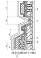
続いて、折り曲げられる前の状態における、画素アレイ部206の図面上右側の端部付近の断面構成について説明する。図3は、図2のIII-III断面を示す図である。
Next, a cross-sectional configuration near the right end portion of the
図3に示すように、表示パネル130は、裏保護フィルム300と、接着層302と、絶縁基板200と、半導体層304と、ゲート絶縁膜308と、第1配線層310と、第1無機絶縁膜312と、第2配線層314と、有機平坦化膜316と、第2無機絶縁膜318と、下部電極320と、有機バンク322と、有機EL膜324と、上部電極326と、封止膜333と、表保護フィルム334と、を含む。
As shown in FIG. 3, the
裏保護フィルム300は、絶縁基板200の裏側を保護するフィルムである。具体的には、裏保護フィルム300は、ポリエチレンテレフタレートやポリプロピレンで形成されたフィルムである。裏保護フィルム300は、折り曲げ部208を含む絶縁基板200の裏面全体に接着層302で貼り合わされる。裏保護フィルム300は、折り曲げ部208が折り曲げにくくならないように薄く形成される。
The back
絶縁基板200は、表示パネル130の基材となる基板またはフィルムである。具体的には、絶縁基板200は、ポリイミドやポリエチレンテレフタラート等の可撓性を有する材料で形成された基板又はフィルムである。なお、絶縁基板200の表面は、窒化膜と酸化膜を積層して形成される無機膜(図示なし)で覆う構成としてもよい。
The insulating
半導体層304は、絶縁基板200の上に配置される。具体的には、半導体層304は、トランジスタ306が形成される画素アレイ部206及び周辺回路210に配置される。また、絶縁基板200の表面に無機膜が配置される場合には、半導体層304は、無機膜の上に配置される。
The
画素回路及び周辺回路210に含まれるトランジスタ306のチャネル領域、ソース領域及びドレイン領域は、半導体層304によって形成される。周辺回路210に用いられるトランジスタ306が折り曲げ部208の外側に配置される構成とすることによって、表示パネル130の額縁を狭くすることができる。画素回路については後述する。
The channel region, source region, and drain region of the
ゲート絶縁膜308は、半導体層304の上に配置される。具体的には、例えば、ゲート絶縁膜308は、シリコン酸化物によって形成され、半導体層304及び絶縁基板200の上に配置される。
The
第1配線層310は、ゲート絶縁膜308の上に配置される。具体的には、第1配線層310は、半導体層304が配置された領域の上側の領域、及び、折り曲げ部208に配置される。折り曲げ部208に配置された第1配線層310は、周辺回路210が生成した信号や第1配線基板202から供給される電源を、画素アレイ部206に供給する。また、第1配線層310は、画素回路及び周辺回路210に含まれるトランジスタ306のゲート電極として用いられる。
The
第1無機絶縁膜312は、第1配線層310の上に配置される。具体的には、第1無機絶縁膜312は、窒化膜と酸化膜を積層して形成され、第1配線層310とゲート絶縁膜308の上に配置される。
The first inorganic insulating
第2配線層314は、第1無機絶縁膜312の上に配置される。具体的には、第2配線層314は、Mo、Al及びMoを積層して形成され、第1無機絶縁膜312の上に配置される。また、第2配線層314は、第1無機絶縁膜312に設けられたコンタクトホールを介して、半導体層304と下部電極320とを電気的に接続する。
The
有機平坦化膜316は、第2配線層314の上側に配置される。具体的には、有機平坦化膜316は、ポリイミドやアクリル樹脂等によって形成され、第2配線層314と第1無機絶縁膜312の上に配置される。有機平坦化膜316は、有機平坦化膜316の下層の段差を平坦にする。
The
第2無機絶縁膜318は、有機平坦化膜316の上に配置される。具体的には、第2無機絶縁膜318は、防湿性及び絶縁性を有する材料で形成され、有機平坦化膜316の上に配置される。例えば、第2無機絶縁膜318は、窒化膜と酸化膜を積層して形成される。第2無機絶縁膜318によって、有機平坦化膜316を介した有機EL膜324への水分浸入を防止できる。
The second inorganic insulating
下部電極320は、第2無機絶縁膜318の上に配置される。具体的には、下部電極320は、酸化インジウム・スズ(Indium Tin Oxide)によって形成され、第2無機絶縁膜318の上に配置される。下部電極320は、第2無機絶縁膜318及び有機平坦化膜316を貫通するコンタクトホール(図示なし)を介して、トランジスタ306のソース電極またはドレイン電極と電気的に接続される。下部電極320は、各画素に配置される有機EL素子516のアノード端子に相当する。なお、下部電極320と第2無機絶縁膜318の間に、MgAg等の光を反射する材料で形成された反射膜を設ける構成としてもよい。
The
有機バンク322は、下部電極320の上に配置される。具体的には、有機バンク322は、下部電極320の上に副画素500の境界に沿って配置される。また、有機バンク322は、下部電極320の上面の一部を露出し周辺を覆うよう有機EL膜324の発光面の位置に開口部を有するように形成される。
The
有機EL膜324は、有機バンク322の上に配置される。具体的には、有機EL膜324は、有機バンク322に設けられた開口部の底部で、下部電極320と接するように配置される。有機EL膜324は、ホール注入層、ホール輸送層、発光層、電子輸送層、電子注入層等を含んで形成される。発光層は、副画素500毎に、赤色、緑色及び青色の光を発する材料を用いて形成される。
The
上部電極326は、有機EL膜324の上に配置される。具体的には、上部電極326は、有機EL膜324の上に、画素アレイ部206から陰極コンタクト部336にかけて配置される。陰極コンタクト部336は、画素アレイ部206と折り曲げ部208の間に設けられる領域である。陰極コンタクト部336において、上部電極326と、折り曲げ部208に配置された下部電極320と、が電気的に接続される。
The
上部電極326は、折り曲げ部208に配置された下部電極320を介して、周辺回路210または第1配線基板202から電源が供給される。これにより、上部電極326は、各副画素500に配置される有機EL素子516のカソード端子として機能する。また、上部電極326は、有機EL膜324が発する光を透過する材料で形成される。例えば、上部電極326は酸化インジウム亜鉛や酸化インジウム・スズなどの透明導電材で形成される。有機バンクに開口が設けられた領域において、下部電極320、有機EL膜324及び上部電極326によって発光素子327が形成される。なお、発光素子327は、図6における有機EL素子516に相当する。
The
封止膜333は、折り曲げ部208を避けて配置されるとともに、画素アレイ部206及び周辺回路210に対する水分子の侵入を防止する。封止膜333は、第1無機封止膜328と、有機封止膜330と、第2無機封止膜332と、を積層して形成される。
The sealing
具体的には、第1無機封止膜328は、画素アレイ部206において、上部電極326を覆うように配置される。また、第1無機封止膜328は、折り曲げ部208の内側であって、画素アレイ部206の外側の領域において、上部電極326、下部電極320及び有機バンク322を覆うように配置される。さらに、第1無機封止膜328は、周辺回路210において、トランジスタ306の上側に配置される。
Specifically, the first
有機封止膜330は、画素アレイ部206において、第1無機封止膜328を覆うように配置される。また、有機封止膜330は、折り曲げ部208の内側であって、画素アレイ部206の外側の領域の一部において、第1無機封止膜328の上側に配置される。さらに、有機封止膜330は、周辺回路210に設けられた第1無機封止膜328の一部の上に配置される。
The
第2無機封止膜332は、画素アレイ部206において、有機封止膜330を覆うように配置される。また、第2無機封止膜332は、折り曲げ部208の内側であって、画素アレイ部206の外側の領域において、有機封止膜330と第1無機封止膜328を覆うように配置される。さらに、第2無機封止膜332は、周辺回路210において、有機封止膜330と第1無機封止膜328を覆うように配置される。
The second
第1無機封止膜328及び第2無機封止膜332は、ケイ素(Si)と、酸素(O)、窒素(N)又は炭素(C)との化合物で形成された無機絶縁材料によって形成される。具体的には、例えば、第1無機封止膜328及び第2無機封止膜332は、シリコン酸化膜(SiO)、シリコン窒化膜(SiN)、シリコン炭化膜(SiC)、シリコン酸窒化膜(SiON)、シリコン炭窒化膜(SiCN)、シリコン酸炭窒化膜(SiOCN)である。また、有機封止膜330は、アクリル、エポキシ、シロキサン系の樹脂で形成された有機材料である。
The first
表保護フィルム334は、封止膜333の上側に接着層302で貼り合わされる。具体的には、表保護フィルム334は、画素アレイ部206、折り曲げ部208及び周辺回路210を覆うように配置される。表保護フィルム334は、裏保護フィルム300と同じ材料で形成される。表保護フィルム334は、折り曲げ部208が折り曲げにくくならないように薄く形成される。また、表示パネル130の左右の額縁において、表保護フィルム334の端部は、絶縁基板200の端部と一致するように配置される。
The surface
さらに、折り曲げ部208の内側及び周辺回路210において、第1無機封止膜328と第2無機封止膜332が接して配置される領域が設けられる。当該構成によれば、封止膜333の端部において、有機封止膜330が露出しないため、有機封止膜330の端部から水分が侵入することを防止できる。
Further, in the inside of the
また、封止膜333が折り曲げ部208を避けて配置されるため、折り曲げ部208が折り曲げにくくなることを防止できる。これにより、折り曲げ部208に配置された第1配線層310の断線及び短絡が生じにくくすることができる。なお、陰極コンタクト部336は、図2における画素アレイ部206と折り曲げ部208の間にある枠状の領域の一部に配置される。
Further, since the sealing
続いて、画素アレイ部206の図面上下側の端部付近の断面構成について説明する。図4は、図2のIV-IV断面を示す図である。
Subsequently, a cross-sectional configuration near the upper and lower ends of the
裏保護フィルム300は、図2で示した構成と同様に、折り曲げ部208を含む絶縁基板200の裏面全体に接着層302で貼り合わされる。絶縁基板200は、図2で示した構成と同様に、無機膜で覆うようにしてもよい。半導体層304は、トランジスタ306が形成される画素アレイ部206及び周辺回路210に配置される。ゲート絶縁膜308は、半導体層304及び絶縁基板200を覆うように配置される。
The back
第1配線層310は、半導体層304が配置された領域の上側の領域、及び、折り曲げ部208に配置される。図2で示した構成と同様に、折り曲げ部208に配置された第1配線層310は、周辺回路210が生成した信号や駆動用半導体212から供給される電源等を、画素アレイ部206に供給する。第1無機絶縁膜312、第2配線層314、有機平坦化膜316及び第2無機絶縁膜318は、図3で示した構成と同様であるため説明を省略する。
The
周辺回路210の端部において、第1配線基板202の第1無機絶縁膜312の上に、第1配線基板202が配置される。具体的には、第1配線基板202は、第1無機絶縁膜312の上に、ACF(Anisotropic Conductive Film)を用いて圧着される。第1配線基板202と第1無機絶縁膜312が圧着される領域の一部において、第1無機絶縁膜312には、開口部(図示なし)が設けられる。当該開口部において、第1配線基板202に設けられた端子部(図示なし)は、ACFを介して第1配線層310と電気的に接続される。
At the end of the
また、駆動用半導体212は、第1配線基板202の上に配置される。具体的には、例えば、駆動用半導体212のバンプ(図示なし)は、第1配線基板202に設けられた配線と電気的に接続される。駆動用半導体212は、折り曲げ部208が折り曲げられることによって、画素アレイ部206の裏面に配置される。なお、駆動用半導体212は、図面上、第1配線基板202の下側に配置されてもよい。
Further, the driving
第3無機絶縁膜400は、陰極コンタクト部336に配置された第2配線層314を覆うように配置される。具体的には、第3無機絶縁膜400は、第1無機絶縁膜312または第2無機絶縁膜318と同じ材料で形成され、陰極コンタクト部336に配置された第2配線層314を覆うように配置される。
The third inorganic insulating
第3無機絶縁膜400によって、第2配線層314と下部電極320との短絡を防止できる。なお、第3無機絶縁膜400の代わりに、第2無機絶縁膜318が第2配線層314を覆う構成としてもよい。下部電極320、有機バンク322、有機EL膜324、上部電極326及び封止膜333の構成は、図2で示した構成と同様であるため説明を省略する。
The third inorganic insulating
表保護フィルム334は、封止膜333の上に接着層302で貼り合わされる。具体的には、表保護フィルム334は、画素アレイ部206、陰極コンタクト部336及び折り曲げ部208の一部を覆うように配置される。
The surface
上記のように、画素アレイ部206の下側においても、封止膜333が折り曲げ部208を避けて配置されるため、折り曲げ部208が折り曲げにくくなることを防止できる。これにより、折り曲げ部208に配置された第1配線層310の断線及び短絡が生じにくくすることができる。また、接着層302や表保護フィルム334が折り曲げ部208で途切れていることで、折り曲げ部を折り返す作業がスムーズに実行できる。
As described above, since the sealing
なお、周辺回路210が画素アレイ部206の下側には配置されない場合には、折り曲げ部208の外側に配置される半導体層304、第1配線層310、第2配線層314及び封止膜333は省略してもよい。
If the
図5は、折り曲げ部208の近傍における表示パネル130の模式的な断面を示す図である。図5に示すように、表示パネル130は、絶縁基板200と、第1配線基板202と、第2配線基板204と、駆動用半導体212と、表保護フィルム334と、偏光板51と、第1補強フィルム52と、熱拡散シート53と、スペーサ54と、第2補強フィルム55と、を含む。なお、図5においては、裏保護フィルム300、接着層302及び半導体層304乃至接着層302の構成の記載を省略する。
FIG. 5 is a diagram showing a schematic cross section of the
絶縁基板200は、折り曲げ部208において折り曲げられる。第2配線基板204は、スペーサ54の下側に配置される。第1配線基板202は、絶縁基板200及び第2配線基板204を繋ぐように配置される。駆動用半導体212は、折り曲げ部208が折り曲げられることによって、第1配線基板202の図面上下側に配置される。なお、駆動用半導体212は、第1配線基板202の上側に配置されてもよい。
The insulating
表保護フィルム334は、上述のように、表示パネル130を保護するフィルムである。表保護フィルム334が表示パネル130の平坦な領域にのみ配置されることにより、折り曲げ部208を折り曲げる作業が容易となる。
As described above, the front
偏光板51は、表示パネル130に入射した外光の反射を低減する。これにより、表示パネル130の視認性が向上する。
The
第1補強フィルム52は、表示パネル130を補強するフィルムである。第1補強フィルム52は、湾曲された状態の表示パネル130の平坦な領域に配置される。具体的には、第1補強フィルム52は、表示パネル130の画素アレイ部206の裏面に配置される。
The first reinforcing
熱拡散シート53は、表示パネル130の熱を拡散するシートである。具体的には、熱拡散シート53は、表示パネル130の周囲に配置された駆動回路で生じた熱を、表示パネル130全体に拡散する。これにより、表示パネル130の一部だけ高温になる状態を防止する。
The
スペーサ54は、折り曲げられた表示パネル130の表面側の部分と裏面側の部分との間に配置される。スペーサ54は、表面側の部分と裏面側の部分との間隔を一定以上に保つ。これにより、表示パネル130に厚み方向の圧力が加わっても折り曲げ部208の曲率が許容範囲に保たれる。
The
また、スペーサ54の端部は、折り曲げ部208の背面に応じた曲率の曲面となるように形成される。スペーサ54の端部を折り曲げ部208の背面に当接させることで、折り曲げ部208の表面に圧力が加わっても折り曲げ部208の形状を一定に保つことができる。
Further, the end portion of the
第2補強フィルム55は、表示パネル130を補強するフィルムである。第2補強フィルム55は、湾曲された状態の表示パネル130の折り曲げ部208に配置される。第2補強フィルム55は、第1補強フィルム52よりも曲げやすい材質及び厚さで形成される。
The second reinforcing
なお、折り曲げ部208には第2補強フィルム55を貼り付けない構成としてもよい。当該構成によれば、折り曲げ部208の柔軟性を増し、より小さい曲率半径で表示パネル130を湾曲させることができる。折り曲げ部208の曲率半径が小さくなるほど、折り曲げられた表示パネル130の平面視でのサイズも小さくなり、また折り曲げられた表示パネル130の厚さも小さくなる。
The second reinforcing
なお、スペーサ54は省略してもよい。具体的には、スペーサ54を省略し、折り曲げ部208をより鋭角に折り曲げる構成としてもよい。当該構成によれば、表示パネル130を薄くすることができる。
The
以上のように、画素アレイ部206から見て折り曲げ部208より先の第1配線基板202及び第2配線基板204を画素アレイ部206の裏側に折り返すことができる。このように折り返すことで、表示装置100の平面視のサイズを小さくすることができ、表示装置100の小型化を図ることができる。また、表示パネル130のうち絶縁基板200の折り曲げ部208から先の部分が裏面に隠れることにより、表示パネル130の正面に占める画素アレイ部206の割合を大きくすることができる。
As described above, the
さらに、駆動用半導体212などを表示パネル130のうち裏面に折り返される部分に搭載し、表示面側の端部はIC等の部品の配置領域として用いないようにすることができる。これにより、額縁の面積を小さくできる。すなわち、表示装置100の狭額縁化を進めることができる。
Further, the driving
続いて、画素アレイ部206を構成する各副画素500に配置される画素回路について説明する。図6は、副画素500に形成される回路を示す図である。図6に示すように、副画素500は、ゲート信号線501と、映像信号線502と、リセット電源線504と、リセット信号線506と、発光制御信号線508と、画素選択トランジスタ510と、保持容量512と、補助容量513と、駆動トランジスタ514と、有機EL素子516と、カソード端子518と、電源520と、発光制御トランジスタ522と、リセットトランジスタ524と、を含んで構成される。
Subsequently, a pixel circuit arranged in each sub-pixel 500 constituting the
ゲート信号線501は、画素選択トランジスタ510のゲート端子と接続される。具体的には、ゲート信号線501は、周辺回路210と画素選択トランジスタ510のゲート端子とを電気的に接続する。また、ゲート信号線501は、周辺回路210から取得した画素選択信号を画素選択トランジスタ510のゲート端子に供給する。
The
映像信号線502は、画素選択トランジスタ510のソース端子又はドレイン端子の一方と接続される。具体的には、映像信号線502は、駆動用半導体212と画素選択トランジスタ510のソース端子又はドレイン端子の一方とを電気的に接続する。また、映像信号線502は、駆動用半導体212から取得した映像信号に応じた電圧を画素選択トランジスタ510のソース端子又はドレイン端子の一方に供給する。
The
リセット電源線504は、リセットトランジスタ524のソース端子又はドレイン端子の一方と接続される。具体的には、リセット電源線504は、駆動用半導体212とリセットトランジスタ524のソース端子又はドレイン端子の一方とを電気的に接続する。また、リセット電源線504は、駆動用半導体212から取得したリセット信号に応じた電圧をリセットトランジスタ524のソース端子又はドレイン端子の一方に供給する。
The
リセット信号線506は、リセットトランジスタ524のゲート端子と接続される。具体的には、リセット信号線506は、駆動用半導体212とリセットトランジスタ524のゲート端子とを電気的に接続する。また、リセット電源線504は、駆動用半導体212から取得したリセット信号をリセットトランジスタ524のゲート端子に供給する。
The
発光制御信号線508は、発光制御トランジスタ522のゲート端子と接続される。具体的には、発光制御信号線508は、周辺回路210と発光制御トランジスタ522のゲート端子と電気的に接続する。また、発光制御信号線508は、周辺回路210から取得した発光制御信号を発光制御トランジスタ522のゲート端子に供給する。
The light emission
画素選択トランジスタ510は、保持容量512に蓄えられる映像信号に基づいた電圧入力を制御する。具体的には、画素選択トランジスタ510は、ゲート端子に印加される電圧がハイ状態又はロー状態のいずれか一方の状態で、画素選択トランジスタ510のソース端子とドレイン端子を導通する(以下、オン状態とする)。画素選択トランジスタ510は、ゲート端子に供給されるゲート信号の状態に応じて、映像信号線502の電圧を保持容量512に供給する。これにより、画素選択トランジスタ510は、映像信号に基づいて、保持容量512に蓄えられる電圧を制御する。
The
保持容量512は、映像信号線502から供給された電圧を保持する。具体的には、保持容量512は、画素選択トランジスタ510がオン状態であるタイミングで、映像信号線502の電圧と同電位となる。その後、ゲート信号によって、画素選択トランジスタ510は、ソース端子とドレイン端子が電気的に遮断された状態(以下、オフ状態とする)となる。保持容量512は、次に画素選択トランジスタ510またはリセットトランジスタ524がオン状態となるまで、フローティング状態となるため、映像信号線502から供給された電圧を保持する。
The holding
駆動トランジスタ514は、画素選択トランジスタ510、保持容量512、発光制御トランジスタ522、及び、有機EL素子516と接続される。具体的には、駆動トランジスタ514のゲート端子は、画素選択トランジスタ510のソース端子又はドレイン端子、及び、保持容量512と電気的に接続される。駆動トランジスタ514のソース端子又はドレイン端子の一方は、発光制御トランジスタ522のソース端子またはドレイン端子と電気的に接続される。また、駆動トランジスタ514のソース端子又はドレイン端子の他の一方は、保持容量512、補助容量513、有機EL素子516のアノード端子、及び、リセットトランジスタ524のソース端子またはドレイン端子の一方と電気的に接続される。
The
また、駆動トランジスタ514は、有機EL素子516に電流を供給する。具体的には、駆動トランジスタ514は、保持容量512に印加された電圧に応じて、電源520から供給される電流を有機EL素子516に供給する。
Further, the
有機EL素子516は、電流を供給されることで発光する。具体的には、有機EL素子516は、保持容量512に保持された電圧に応じた電流が、駆動トランジスタ514によって供給されることで発光する。なお、有機EL素子516は、上述の下部電極320、有機EL膜324及び上部電極326によって構成される。
The
カソード端子518は、有機EL素子516と電気的に接続される。具体的には、カソード端子518は、有機EL素子516のカソード端子と電気的に接続される。また、カソード端子518は、電源520との間で電圧を印加されることにより、有機EL素子516に電流を供給する。なお、カソード端子518は、上述の上部電極326に相当する。
The
電源520は、発光制御トランジスタ522と接続され、有機EL素子516に電流を供給する。具体的には、電源520は、発光制御トランジスタ522のソース端子またはドレイン端子と電気的に接続される。また、電源520は、駆動用半導体212または周辺回路210と接続され、一定の電圧が印加される。これにより、電源520は、駆動トランジスタ514及び発光制御トランジスタ522がオン状態であるときに、有機EL素子516に電流を供給する。
The
発光制御トランジスタ522は、有機EL素子516に対する電源520の供給を遮断するか否かを制御する。具体的には、発光制御トランジスタ522のソース端子またはドレイン端子の一方は、電源520に接続され、他の一方は、駆動トランジスタ514のソース端子又はドレイン端子と電気的に接続される。また、駆動トランジスタ514のゲート端子は、発光制御信号線508と電気的に接続される。
The light
発光制御トランジスタ522は、発光制御信号線508から供給される発光制御信号によって、オン状態またはオフ状態となるように制御される。発光制御トランジスタ522がオン状態の場合、発光制御トランジスタ522は、電源520から供給される電流を、駆動トランジスタ514を介して有機EL素子516に供給する。一方、発光制御トランジスタ522がオフ状態の場合、発光制御トランジスタ522は、有機EL素子516に対する電源520の供給を遮断する。
The light
リセットトランジスタ524は、保持容量512に保持された電圧をリセットするタイミングを制御する。具体的には、リセットトランジスタ524のゲート端子は、リセット信号線506と接続される。リセットトランジスタ524のソース端子又はドレイン端子の一方は、リセット電源線504と接続される。リセットトランジスタ524のソース端子又はドレイン端子の他の一方は、保持容量512、補助容量513、有機EL素子516のアノード端子及び駆動トランジスタ514のソース端子又はドレイン端子の一方と接続される。
The
リセットトランジスタ524は、保持容量512及び補助容量513に保持された電圧が、初期状態の電圧となるように制御する。具体的には、リセットトランジスタ524は、リセット信号線506から供給されるリセット信号によって、オン状態またはオフ状態となるように制御される。リセットトランジスタ524がオン状態の場合、保持容量512及び補助容量513は、初期状態の電圧であるリセット電源線504の電圧が供給される。保持容量512及び補助容量513に保持された電圧が初期状態の電圧となった後、画素選択トランジスタ510がオン状態となることで、保持容量512及び補助容量513に保持される電圧が変更される。
The
以上のように、折り曲げ部208に配置された第1配線層310を介して、周辺回路210又は駆動用半導体212が生成した信号又は電源520が画素回路に供給される。これにより、表示パネル130は、画素アレイ部206に画像を表示する。
As described above, the signal or
本発明の思想の範疇において、当業者であれば、各種の変更例及び修正例に想到し得るものであり、それら変更例及び修正例についても本発明の範囲に属するものと了解される。例えば、前述の各実施形態に対して、当業者が適宜、構成要素の追加、削除若しくは設計変更を行ったもの、又は、工程の追加、省略若しくは条件変更を行ったものも、本発明の要旨を備えている限り、本発明の範囲に含まれる。 In the scope of the idea of the present invention, those skilled in the art can come up with various modified examples and modified examples, and it is understood that these modified examples and modified examples also belong to the scope of the present invention. For example, a person skilled in the art appropriately adds, deletes, or changes the design of each of the above-described embodiments, or adds, omits, or changes the conditions of the process, which is the gist of the present invention. Is included in the scope of the present invention as long as it is provided.
100 表示装置、110 上フレーム、120 下フレーム、130 表示パネル、200 絶縁基板、202 第1配線基板、204 第2配線基板、206 画素アレイ部、208 折り曲げ部、210 周辺回路、212 駆動用半導体、300 裏保護フィルム、302 接着層、304 半導体層、306 トランジスタ、308 ゲート絶縁膜、310 第1配線層、312 第1無機絶縁膜、314 第2配線層、316 有機平坦化膜、318 第2無機絶縁膜、320 下部電極、322 有機バンク、324 有機EL膜、326 上部電極、327 発光素子、328 第1無機封止膜、330 有機封止膜、332 第2無機封止膜、333 封止膜、334 表保護フィルム、336 陰極コンタクト部、400 第3無機絶縁膜、51 偏光板、52 第1補強フィルム、53 熱拡散シート、54 スペーサ、55 第2補強フィルム、500 副画素、501 ゲート信号線、502 映像信号線、504 リセット電源線、506 リセット信号線、508 発光制御信号線、510 画素選択トランジスタ、512 保持容量、513 補助容量、514 駆動トランジスタ、516 有機EL素子、518 カソード端子、520 電源、522 発光制御トランジスタ、524 リセットトランジスタ。
100 Display device, 110 Upper frame, 120 Lower frame, 130 Display panel, 200 Insulation board, 202 1st wiring board, 204 2nd wiring board, 206 pixel array part, 208 Bending part, 210 Peripheral circuit, 212 Drive semiconductor, 300 Back protective film, 302 adhesive layer, 304 semiconductor layer, 306 transistor, 308 gate insulating film, 310 1st wiring layer, 312 1st inorganic insulating film, 314 2nd wiring layer, 316 organic flattening film, 318 2nd inorganic Insulation film, 320 lower electrode, 322 organic bank, 324 organic EL film, 326 upper electrode, 327 light emitting device, 328 first inorganic sealing film, 330 organic sealing film, 332 second inorganic sealing film, 333
Claims (5)
少なくとも前記画素アレイ部の外側に配置されて折り曲げられる折り曲げ部と、
前記折り曲げ部によって前記画素アレイ部と連結され、前記複数の画素に供給する信号を生成する周辺回路と、
前記折り曲げ部を避けて配置されるとともに、前記画素アレイ部及び前記周辺回路に対する水分子の侵入を防止する封止膜と、
前記封止膜を保護する保護フィルムと、
を有し、
前記封止膜は、第1無機封止膜と、第2無機封止膜と、前記第1無機封止膜と前記第2無機封止膜との間の有機封止膜と、を有し、
前記封止膜は、前記画素アレイ部を覆う第1領域と、前記周辺回路を覆う第2領域と、
を有し、
前記第1領域に設けられた前記有機封止膜と、前記第2領域に設けられた前記有機封止膜とはそれぞれ、前記第1無機封止膜と前記第2無機封止膜とによって、前記有機封止膜が前記封止膜の端部において露出しないように封じられ、
前記保護フィルムは、前記第1領域、前記折り曲げ部及び前記第2領域に亘って連続的に配置されると共に、前記折り曲げ部における上面の高さが、前記第1領域及び前記第2領域における上面の高さのいずれよりも低くなるように形成される、ことを特徴とする表示装置。 A pixel array unit composed of a plurality of pixels arranged in a matrix, and
At least a bent portion that is arranged and bent outside the pixel array portion,
A peripheral circuit that is connected to the pixel array portion by the bent portion and generates a signal to be supplied to the plurality of pixels.
A sealing film that is arranged so as to avoid the bent portion and prevents water molecules from entering the pixel array portion and the peripheral circuit.
A protective film that protects the sealing film and
Have,
The sealing film has a first inorganic sealing film, a second inorganic sealing film, and an organic sealing film between the first inorganic sealing film and the second inorganic sealing film. ,
The sealing film includes a first region that covers the pixel array portion, a second region that covers the peripheral circuit, and the like.
Have,
The organic sealing film provided in the first region and the organic sealing film provided in the second region are formed by the first inorganic sealing film and the second inorganic sealing film, respectively. The organic sealing film is sealed so as not to be exposed at the end of the sealing film .
The protective film is continuously arranged over the first region, the bent portion, and the second region, and the height of the upper surface of the bent portion is the upper surface of the first region and the second region. A display device characterized in that it is formed to be lower than any of the heights of .
前記周辺回路は、前記複数の画素にそれぞれ含まれる副画素から、電流を供給する副画素を選択する選択信号を生成する選択信号生成回路を含むことを特徴とする請求項1または2に記載の表示装置。 The plurality of pixels are composed of a plurality of sub-pixels that emit light of different colors.
The peripheral circuit according to claim 1 or 2, wherein the peripheral circuit includes a selection signal generation circuit that generates a selection signal for selecting a sub-pixel to supply a current from the sub-pixels included in the plurality of pixels. Display device.
Priority Applications (2)
| Application Number | Priority Date | Filing Date | Title |
|---|---|---|---|
| JP2017075519A JP7002855B2 (en) | 2017-04-05 | 2017-04-05 | Display device |
| US15/940,086 US10553666B2 (en) | 2017-04-05 | 2018-03-29 | Display device |
Applications Claiming Priority (1)
| Application Number | Priority Date | Filing Date | Title |
|---|---|---|---|
| JP2017075519A JP7002855B2 (en) | 2017-04-05 | 2017-04-05 | Display device |
Publications (3)
| Publication Number | Publication Date |
|---|---|
| JP2018180100A JP2018180100A (en) | 2018-11-15 |
| JP2018180100A5 JP2018180100A5 (en) | 2020-05-14 |
| JP7002855B2 true JP7002855B2 (en) | 2022-01-20 |
Family
ID=63711214
Family Applications (1)
| Application Number | Title | Priority Date | Filing Date |
|---|---|---|---|
| JP2017075519A Active JP7002855B2 (en) | 2017-04-05 | 2017-04-05 | Display device |
Country Status (2)
| Country | Link |
|---|---|
| US (1) | US10553666B2 (en) |
| JP (1) | JP7002855B2 (en) |
Families Citing this family (10)
| Publication number | Priority date | Publication date | Assignee | Title |
|---|---|---|---|---|
| US10727424B2 (en) * | 2017-04-27 | 2020-07-28 | Sharp Kabushiki Kaisha | Flexible display device |
| KR102482991B1 (en) * | 2017-12-28 | 2022-12-29 | 엘지디스플레이 주식회사 | Top Emission Type Organic Light Emitting Diode Display |
| US10566555B2 (en) * | 2018-01-30 | 2020-02-18 | Wuhan China Star Optoelectronics Semiconductor Display Technology Co., Ltd. | Organic light emitting diode (OLED) display panel and the manufacturing method thereof |
| CN109638060B (en) * | 2018-12-21 | 2020-10-27 | 武汉华星光电半导体显示技术有限公司 | Array substrate and flexible display panel |
| CN109742118B (en) * | 2019-01-08 | 2022-04-29 | 京东方科技集团股份有限公司 | Display panel, array substrate and preparation method thereof |
| CN110010010A (en) * | 2019-04-30 | 2019-07-12 | 昆山工研院新型平板显示技术中心有限公司 | Signal line structure, display panel and display device |
| CN110610968B (en) * | 2019-08-28 | 2021-09-03 | 武汉华星光电半导体显示技术有限公司 | Display panel and display device |
| US11335258B2 (en) * | 2020-04-29 | 2022-05-17 | Dell Products L.P. | Information handling system thin display with minimal bezel |
| KR20220069731A (en) * | 2020-11-20 | 2022-05-27 | 엘지디스플레이 주식회사 | Display device |
| KR20230050545A (en) * | 2021-10-07 | 2023-04-17 | 삼성디스플레이 주식회사 | Display device |
Citations (8)
| Publication number | Priority date | Publication date | Assignee | Title |
|---|---|---|---|---|
| JP2004047411A (en) | 2001-11-09 | 2004-02-12 | Semiconductor Energy Lab Co Ltd | Light emitting device and manufacturing method thereof |
| JP2004102245A (en) | 2002-07-18 | 2004-04-02 | Seiko Epson Corp | Electro-optical device, wiring board, and electronic apparatus |
| JP2011008969A (en) | 2009-06-23 | 2011-01-13 | Canon Inc | Display |
| JP2011034066A (en) | 2009-07-07 | 2011-02-17 | Semiconductor Energy Lab Co Ltd | Display |
| WO2013069236A1 (en) | 2011-11-08 | 2013-05-16 | パナソニック株式会社 | Method for manufacturing light-emitting panel and display device provided with light-emitting panel obtained by same manufacturing method |
| US20140306941A1 (en) | 2013-04-11 | 2014-10-16 | Lg Display Co., Ltd. | Flexible display panel |
| US20160064691A1 (en) | 2014-08-29 | 2016-03-03 | Samsung Display Co., Ltd. | Display apparatus and method of manufacturing the same |
| US20160204183A1 (en) | 2015-01-09 | 2016-07-14 | Apple Inc. | Organic Light-Emitting Diode Display With Bent Substrate |
Family Cites Families (3)
| Publication number | Priority date | Publication date | Assignee | Title |
|---|---|---|---|---|
| JP2011209405A (en) | 2010-03-29 | 2011-10-20 | Sony Corp | Display device and electronic device |
| US10210798B2 (en) * | 2016-07-04 | 2019-02-19 | Samsung Display Co., Ltd. | Display device having protective structure |
| KR102556022B1 (en) * | 2016-07-06 | 2023-07-17 | 삼성디스플레이 주식회사 | Flexible display device |
-
2017
- 2017-04-05 JP JP2017075519A patent/JP7002855B2/en active Active
-
2018
- 2018-03-29 US US15/940,086 patent/US10553666B2/en active Active
Patent Citations (8)
| Publication number | Priority date | Publication date | Assignee | Title |
|---|---|---|---|---|
| JP2004047411A (en) | 2001-11-09 | 2004-02-12 | Semiconductor Energy Lab Co Ltd | Light emitting device and manufacturing method thereof |
| JP2004102245A (en) | 2002-07-18 | 2004-04-02 | Seiko Epson Corp | Electro-optical device, wiring board, and electronic apparatus |
| JP2011008969A (en) | 2009-06-23 | 2011-01-13 | Canon Inc | Display |
| JP2011034066A (en) | 2009-07-07 | 2011-02-17 | Semiconductor Energy Lab Co Ltd | Display |
| WO2013069236A1 (en) | 2011-11-08 | 2013-05-16 | パナソニック株式会社 | Method for manufacturing light-emitting panel and display device provided with light-emitting panel obtained by same manufacturing method |
| US20140306941A1 (en) | 2013-04-11 | 2014-10-16 | Lg Display Co., Ltd. | Flexible display panel |
| US20160064691A1 (en) | 2014-08-29 | 2016-03-03 | Samsung Display Co., Ltd. | Display apparatus and method of manufacturing the same |
| US20160204183A1 (en) | 2015-01-09 | 2016-07-14 | Apple Inc. | Organic Light-Emitting Diode Display With Bent Substrate |
Also Published As
| Publication number | Publication date |
|---|---|
| US20180294328A1 (en) | 2018-10-11 |
| US10553666B2 (en) | 2020-02-04 |
| JP2018180100A (en) | 2018-11-15 |
Similar Documents
| Publication | Publication Date | Title |
|---|---|---|
| JP7002855B2 (en) | Display device | |
| JP6636807B2 (en) | Organic EL display | |
| TWI648851B (en) | Display device | |
| EP3188244A1 (en) | Organic light emitting diode display device | |
| EP2105964A1 (en) | Organic light emitting display device | |
| US11765925B2 (en) | Display device | |
| US10268092B2 (en) | Display device | |
| JP2009200025A (en) | Organic electroluminescent display device | |
| KR102610245B1 (en) | Display device and method for manufacturing the display device | |
| JP2019191525A (en) | Display device | |
| JP7271246B2 (en) | Display device | |
| JP2019003040A (en) | Display | |
| KR20170079978A (en) | Transparent display device | |
| US9960388B2 (en) | Display device with light emitting elements and pixel electrodes | |
| KR102533228B1 (en) | Organic light emitting display device | |
| US11574592B2 (en) | Display device | |
| JP7112999B2 (en) | Display device | |
| KR102538361B1 (en) | Organic light emitting display device | |
| KR102610485B1 (en) | Electroluminescent display device | |
| JP7246534B2 (en) | array substrate | |
| JP2019035835A (en) | Display device | |
| KR20200074657A (en) | Organic light emitting display device | |
| KR20200058821A (en) | Organic light emitting display device | |
| KR20170125485A (en) | Organic light emitting display device and method for fabricating the same | |
| JP2007095733A (en) | Electroluminescence device and electronic apparatus |
Legal Events
| Date | Code | Title | Description |
|---|---|---|---|
| A521 | Request for written amendment filed |
Free format text: JAPANESE INTERMEDIATE CODE: A523 Effective date: 20200403 |
|
| A621 | Written request for application examination |
Free format text: JAPANESE INTERMEDIATE CODE: A621 Effective date: 20200403 |
|
| A977 | Report on retrieval |
Free format text: JAPANESE INTERMEDIATE CODE: A971007 Effective date: 20210225 |
|
| A131 | Notification of reasons for refusal |
Free format text: JAPANESE INTERMEDIATE CODE: A131 Effective date: 20210302 |
|
| A521 | Request for written amendment filed |
Free format text: JAPANESE INTERMEDIATE CODE: A523 Effective date: 20210430 |
|
| A131 | Notification of reasons for refusal |
Free format text: JAPANESE INTERMEDIATE CODE: A131 Effective date: 20210928 |
|
| A521 | Request for written amendment filed |
Free format text: JAPANESE INTERMEDIATE CODE: A523 Effective date: 20211129 |
|
| TRDD | Decision of grant or rejection written | ||
| A01 | Written decision to grant a patent or to grant a registration (utility model) |
Free format text: JAPANESE INTERMEDIATE CODE: A01 Effective date: 20211214 |
|
| A61 | First payment of annual fees (during grant procedure) |
Free format text: JAPANESE INTERMEDIATE CODE: A61 Effective date: 20211228 |
|
| R150 | Certificate of patent or registration of utility model |
Ref document number: 7002855 Country of ref document: JP Free format text: JAPANESE INTERMEDIATE CODE: R150 |