JP6991972B2 - Detection chip, detection system and detection method - Google Patents

Detection chip, detection system and detection method Download PDF

Info

Publication number
JP6991972B2
JP6991972B2 JP2018529875A JP2018529875A JP6991972B2 JP 6991972 B2 JP6991972 B2 JP 6991972B2 JP 2018529875 A JP2018529875 A JP 2018529875A JP 2018529875 A JP2018529875 A JP 2018529875A JP 6991972 B2 JP6991972 B2 JP 6991972B2
Authority
JP
Japan
Prior art keywords
light
detection
detection chip
metal film
accommodating portion
Prior art date
Legal status (The legal status is an assumption and is not a legal conclusion. Google has not performed a legal analysis and makes no representation as to the accuracy of the status listed.)
Active
Application number
JP2018529875A
Other languages
Japanese (ja)
Other versions
JPWO2018021238A1 (en
Inventor
智典 金子
剛典 永江
高敏 彼谷
幸登 中村
Current Assignee (The listed assignees may be inaccurate. Google has not performed a legal analysis and makes no representation or warranty as to the accuracy of the list.)
Otsuka Pharmaceutical Co Ltd
Original Assignee
Otsuka Pharmaceutical Co Ltd
Priority date (The priority date is an assumption and is not a legal conclusion. Google has not performed a legal analysis and makes no representation as to the accuracy of the date listed.)
Filing date
Publication date
Application filed by Otsuka Pharmaceutical Co Ltd filed Critical Otsuka Pharmaceutical Co Ltd
Publication of JPWO2018021238A1 publication Critical patent/JPWO2018021238A1/en
Application granted granted Critical
Publication of JP6991972B2 publication Critical patent/JP6991972B2/en
Active legal-status Critical Current
Anticipated expiration legal-status Critical

Links

Images

Classifications

    • GPHYSICS
    • G01MEASURING; TESTING
    • G01NINVESTIGATING OR ANALYSING MATERIALS BY DETERMINING THEIR CHEMICAL OR PHYSICAL PROPERTIES
    • G01N21/00Investigating or analysing materials by the use of optical means, i.e. using sub-millimetre waves, infrared, visible or ultraviolet light
    • G01N21/01Arrangements or apparatus for facilitating the optical investigation
    • G01N21/03Cuvette constructions
    • G01N21/0303Optical path conditioning in cuvettes, e.g. windows; adapted optical elements or systems; path modifying or adjustment
    • BPERFORMING OPERATIONS; TRANSPORTING
    • B01PHYSICAL OR CHEMICAL PROCESSES OR APPARATUS IN GENERAL
    • B01LCHEMICAL OR PHYSICAL LABORATORY APPARATUS FOR GENERAL USE
    • B01L3/00Containers or dishes for laboratory use, e.g. laboratory glassware; Droppers
    • B01L3/50Containers for the purpose of retaining a material to be analysed, e.g. test tubes
    • B01L3/508Containers for the purpose of retaining a material to be analysed, e.g. test tubes rigid containers not provided for above
    • B01L3/5082Test tubes per se
    • GPHYSICS
    • G01MEASURING; TESTING
    • G01NINVESTIGATING OR ANALYSING MATERIALS BY DETERMINING THEIR CHEMICAL OR PHYSICAL PROPERTIES
    • G01N21/00Investigating or analysing materials by the use of optical means, i.e. using sub-millimetre waves, infrared, visible or ultraviolet light
    • G01N21/62Systems in which the material investigated is excited whereby it emits light or causes a change in wavelength of the incident light
    • G01N21/63Systems in which the material investigated is excited whereby it emits light or causes a change in wavelength of the incident light optically excited
    • G01N21/64Fluorescence; Phosphorescence
    • G01N21/645Specially adapted constructive features of fluorimeters
    • G01N21/648Specially adapted constructive features of fluorimeters using evanescent coupling or surface plasmon coupling for the excitation of fluorescence
    • GPHYSICS
    • G01MEASURING; TESTING
    • G01NINVESTIGATING OR ANALYSING MATERIALS BY DETERMINING THEIR CHEMICAL OR PHYSICAL PROPERTIES
    • G01N21/00Investigating or analysing materials by the use of optical means, i.e. using sub-millimetre waves, infrared, visible or ultraviolet light
    • G01N21/62Systems in which the material investigated is excited whereby it emits light or causes a change in wavelength of the incident light
    • G01N21/63Systems in which the material investigated is excited whereby it emits light or causes a change in wavelength of the incident light optically excited
    • G01N21/64Fluorescence; Phosphorescence
    • G01N21/6486Measuring fluorescence of biological material, e.g. DNA, RNA, cells
    • GPHYSICS
    • G01MEASURING; TESTING
    • G01NINVESTIGATING OR ANALYSING MATERIALS BY DETERMINING THEIR CHEMICAL OR PHYSICAL PROPERTIES
    • G01N33/00Investigating or analysing materials by specific methods not covered by groups G01N1/00 - G01N31/00
    • G01N33/48Biological material, e.g. blood, urine; Haemocytometers
    • G01N33/50Chemical analysis of biological material, e.g. blood, urine; Testing involving biospecific ligand binding methods; Immunological testing
    • G01N33/53Immunoassay; Biospecific binding assay; Materials therefor
    • G01N33/543Immunoassay; Biospecific binding assay; Materials therefor with an insoluble carrier for immobilising immunochemicals
    • GPHYSICS
    • G01MEASURING; TESTING
    • G01NINVESTIGATING OR ANALYSING MATERIALS BY DETERMINING THEIR CHEMICAL OR PHYSICAL PROPERTIES
    • G01N33/00Investigating or analysing materials by specific methods not covered by groups G01N1/00 - G01N31/00
    • G01N33/48Biological material, e.g. blood, urine; Haemocytometers
    • G01N33/50Chemical analysis of biological material, e.g. blood, urine; Testing involving biospecific ligand binding methods; Immunological testing
    • G01N33/68Chemical analysis of biological material, e.g. blood, urine; Testing involving biospecific ligand binding methods; Immunological testing involving proteins, peptides or amino acids
    • BPERFORMING OPERATIONS; TRANSPORTING
    • B01PHYSICAL OR CHEMICAL PROCESSES OR APPARATUS IN GENERAL
    • B01LCHEMICAL OR PHYSICAL LABORATORY APPARATUS FOR GENERAL USE
    • B01L2300/00Additional constructional details
    • B01L2300/16Surface properties and coatings
    • B01L2300/168Specific optical properties, e.g. reflective coatings
    • GPHYSICS
    • G01MEASURING; TESTING
    • G01NINVESTIGATING OR ANALYSING MATERIALS BY DETERMINING THEIR CHEMICAL OR PHYSICAL PROPERTIES
    • G01N21/00Investigating or analysing materials by the use of optical means, i.e. using sub-millimetre waves, infrared, visible or ultraviolet light
    • G01N21/17Systems in which incident light is modified in accordance with the properties of the material investigated
    • G01N21/59Transmissivity
    • G01N2021/5903Transmissivity using surface plasmon resonance [SPR], e.g. extraordinary optical transmission [EOT]
    • GPHYSICS
    • G01MEASURING; TESTING
    • G01NINVESTIGATING OR ANALYSING MATERIALS BY DETERMINING THEIR CHEMICAL OR PHYSICAL PROPERTIES
    • G01N21/00Investigating or analysing materials by the use of optical means, i.e. using sub-millimetre waves, infrared, visible or ultraviolet light
    • G01N21/62Systems in which the material investigated is excited whereby it emits light or causes a change in wavelength of the incident light
    • G01N21/63Systems in which the material investigated is excited whereby it emits light or causes a change in wavelength of the incident light optically excited
    • G01N21/64Fluorescence; Phosphorescence
    • G01N21/645Specially adapted constructive features of fluorimeters
    • G01N2021/6482Sample cells, cuvettes

Landscapes

  • Health & Medical Sciences (AREA)
  • Life Sciences & Earth Sciences (AREA)
  • Immunology (AREA)
  • Chemical & Material Sciences (AREA)
  • General Health & Medical Sciences (AREA)
  • Analytical Chemistry (AREA)
  • Pathology (AREA)
  • General Physics & Mathematics (AREA)
  • Physics & Mathematics (AREA)
  • Biochemistry (AREA)
  • Engineering & Computer Science (AREA)
  • Molecular Biology (AREA)
  • Biomedical Technology (AREA)
  • Hematology (AREA)
  • Urology & Nephrology (AREA)
  • Nuclear Medicine, Radiotherapy & Molecular Imaging (AREA)
  • Microbiology (AREA)
  • Medicinal Chemistry (AREA)
  • Cell Biology (AREA)
  • Biotechnology (AREA)
  • Food Science & Technology (AREA)
  • Proteomics, Peptides & Aminoacids (AREA)
  • Clinical Laboratory Science (AREA)
  • Chemical Kinetics & Catalysis (AREA)
  • Investigating, Analyzing Materials By Fluorescence Or Luminescence (AREA)
  • Optical Measuring Cells (AREA)
  • Investigating Or Analysing Materials By Optical Means (AREA)

Description

本発明は、被検出物質を検出するための検出チップ、検出システムおよび検出方法に関する。 The present invention relates to a detection chip, a detection system and a detection method for detecting a substance to be detected.

生化学検査において抗原抗体反応などの生化学反応が利用されている。たとえば、蛍光免疫測定法(以下、「FIA」とも称する)では、被検出物質(抗原)に蛍光物質を含む標識物質を反応させる。その後、蛍光物質で標識された被検出物質に励起光を照射して、蛍光物質が発する蛍光を検出する。そして、検出された蛍光の強度などから、被検出物質の量を特定する。このようなFIAの中でも、特に高感度に被検出物質の検出を行うことが可能な方法として、表面プラズモン励起増強蛍光分光法(Surface Plasmon-field enhanced Fluorescence Spectroscopy、以下「SPFS」とも称する)が知られている(例えば特許文献1参照)。 Biochemical reactions such as antigen-antibody reactions are used in biochemical tests. For example, in a fluorescent immunoassay (hereinafter, also referred to as “FIA”), a labeled substance containing a fluorescent substance is reacted with a substance to be detected (antigen). Then, the substance to be detected labeled with the fluorescent substance is irradiated with excitation light to detect the fluorescence emitted by the fluorescent substance. Then, the amount of the substance to be detected is specified from the intensity of the detected fluorescence and the like. Among such FIA, surface plasmon-field enhanced Fluorescence Spectroscopy (hereinafter, also referred to as "SPFS") is known as a method capable of detecting a substance to be detected with particularly high sensitivity. (See, for example, Patent Document 1).

SPFSでは、被検出物質に特異的に結合できる第1の捕捉体(例えば1次抗体)を金属膜上に固定して、被検出物質を捕捉するための反応場を形成する。たとえば、反応場は、ウェル(液体を収容するための有底の凹部)の底面に配置される。特許文献1に記載の検出システムでは、ウェルは、光透過性を有する誘電体部材の上に形成された金属膜上に、貫通孔を有するウェル部材を固定することで形成されており、反応場は、ウェルの底面を構成する金属膜上に配置されている。そして、このウェルに被検出物質を含む液体(検体)を導入することで、第1の捕捉体に被検出物質を結合させる。次いで、蛍光物質で標識された第2の捕捉体(例えば2次抗体)をウェルに導入することで、第1の捕捉体に結合している被検出物質に、第2の捕捉体をさらに結合させる。つまり、被検出物質を、間接的に蛍光物質で標識する。この状態で誘電体部材側から金属膜に励起光を照射すると、蛍光物質が表面プラズモン共鳴(以下、「SPR」とも称する)により増強された電場により励起され、蛍光を放出する。そして、蛍光物質が放出した蛍光を検出することで、被検出物質を検出できる。特許文献1に記載の検出システムでは、蛍光を検出するための検出部は、ウェルの上方に配置されており、ウェル内の液体の液面を通過した蛍光を検出している。 In SPFS, a first trap (eg, primary antibody) capable of specifically binding to the substance to be detected is immobilized on a metal membrane to form a reaction field for capturing the substance to be detected. For example, the reaction field is located at the bottom of a well (a bottomed recess for containing liquid). In the detection system described in Patent Document 1, the well is formed by fixing a well member having a through hole on a metal film formed on a light-transmitting dielectric member, and is a reaction field. Is arranged on the metal film constituting the bottom surface of the well. Then, by introducing a liquid (sample) containing the substance to be detected into this well, the substance to be detected is bound to the first trap. Then, by introducing a second trap (eg, a secondary antibody) labeled with a fluorescent substance into the well, the second trap is further bound to the detected substance bound to the first trap. Let me. That is, the substance to be detected is indirectly labeled with a fluorescent substance. When the metal film is irradiated with excitation light from the dielectric member side in this state, the fluorescent substance is excited by an electric field enhanced by surface plasmon resonance (hereinafter, also referred to as “SPR”) and emits fluorescence. Then, by detecting the fluorescence emitted by the fluorescent substance, the substance to be detected can be detected. In the detection system described in Patent Document 1, the detection unit for detecting fluorescence is arranged above the well, and detects the fluorescence that has passed through the liquid surface of the liquid in the well.

国際公開第2012/157403号International Publication No. 2012/157403

特許文献1に記載の検出システムでは、ウェルの底面に金属膜および反応場が配置されているため、ウェル内の液体を除去するときに送液器具の先端が金属膜または反応場に接触して、これらが破損してしまうおそれがあった。このため、送液器具の先端をウェルの底面に押し付けることができず、ウェル内の液体を十分に除去することが困難であった。このようにウェル内に液体が残存してしまうと、各種反応が適切に進まず、検出精度が低下してしまうおそれがある。 In the detection system described in Patent Document 1, since the metal film and the reaction field are arranged on the bottom surface of the well, the tip of the liquid feeding device comes into contact with the metal film or the reaction field when removing the liquid in the well. , There was a risk that these would be damaged. Therefore, the tip of the liquid feeding device could not be pressed against the bottom surface of the well, and it was difficult to sufficiently remove the liquid in the well. If the liquid remains in the well in this way, various reactions may not proceed properly and the detection accuracy may decrease.

また、特許文献1に記載の検出システムでは、検出部は、ウェルの上方に配置されており、ウェル内の液体の液面を通過した蛍光を検出している。このため、ウェルの内径が小さい場合は、蛍光の検出結果がメニスカスの影響を受けてしまう。また、ウェルの内径が大きい場合であっても、蛍光の検出結果が液面上に存在する気泡の影響を受けてしまうおそれがある。 Further, in the detection system described in Patent Document 1, the detection unit is arranged above the well and detects the fluorescence that has passed through the liquid surface of the liquid in the well. Therefore, if the inner diameter of the well is small, the fluorescence detection result will be affected by the meniscus. Further, even when the inner diameter of the well is large, the fluorescence detection result may be affected by the bubbles existing on the liquid surface.

本発明の目的は、反応工程中における収容部(ウェル)内の液体の残存による検出精度の低下を抑制することができ、かつ検出工程中における収容部内の液体の液面による検出結果への影響を抑制することができる、被検出物質を検出するための検出チップ、検出システムおよび検出方法を提供することである。 An object of the present invention is to suppress a decrease in detection accuracy due to residual liquid in the accommodating portion (well) during the reaction process, and to affect the detection result by the liquid level of the liquid in the accommodating portion during the detection process. It is an object of the present invention to provide a detection chip, a detection system and a detection method for detecting a substance to be detected, which can suppress the above.

本発明の一実施形態に係る検出チップは、上部および側部に開口を有する収容部を含むウェル本体と、被検出物質を捕捉するための捕捉領域が配置されている側壁部材と、を有し、前記側壁部材は、前記収容部の側部の開口を介して前記捕捉領域の少なくとも一部が前記収容部内に露出し、かつ前記側壁部材が前記収容部の側部の開口の少なくとも一部を閉塞するように、前記ウェル本体に固定されている。 A detection chip according to an embodiment of the present invention has a well body including an accommodating portion having openings at the top and sides, and a side wall member in which a capture region for capturing the substance to be detected is arranged. In the side wall member, at least a part of the trapping area is exposed in the housing portion through the opening of the side portion of the housing portion, and the side wall member exposes at least a part of the opening of the side portion of the housing portion. It is fixed to the well body so as to be closed.

また、本発明の一実施形態に係る検出システムは、上部に開口を有する収容部と、前記収容部を構成する側壁の内面上に金属膜を介さずにまたは金属膜を介して配置された、被検出物質を捕捉するための反応場とを有する検出チップと、前記反応場に対応する位置の前記側壁の内面においてエバネッセント光が生じるように、または前記金属膜において表面プラズモン共鳴が生じるように外部から前記検出チップに光を照射する光源と、前記光源が前記検出チップに光を照射したときに、前記検出チップから放出される光であって、前記反応場に捕捉されている被検出物質の量に応じて光量が変化する光を検出する検出部と、を有する。 Further, the detection system according to the embodiment of the present invention is arranged on the inner surface of the accommodating portion having an opening at the upper portion and the inner surface of the side wall constituting the accommodating portion without or through the metal film. External so that an evanescent light is generated on the inner surface of the side wall at a position corresponding to the reaction field and a detection chip having a reaction field for capturing the substance to be detected, or surface plasmon resonance occurs in the metal film. A light source that irradiates the detection chip with light, and a light emitted from the detection chip when the light source irradiates the detection chip with light, that is, a substance to be detected captured in the reaction field. It has a detection unit for detecting light whose amount of light changes according to the amount of light.

また、本発明の一実施形態に係る検出方法は、上部に開口を有する収容部と、前記収容部を構成する側壁の内面上に金属膜を介さずにまたは金属膜を介して配置された反応場とを有する検出チップの前記反応場に被検出物質を捕捉させる第1工程と、前記反応場に対応する位置の前記側壁の内面においてエバネッセント光が生じるように、または前記金属膜において表面プラズモン共鳴が生じるように外部から前記検出チップに光を照射するとともに、前記検出チップから放出される光であって、前記反応場に捕捉されている被検出物質の量に応じて光量が変化する光を検出する第2工程と、を有する。 Further, in the detection method according to the embodiment of the present invention, the accommodating portion having an opening at the upper portion and the reaction arranged on the inner surface of the side wall constituting the accommodating portion without or through the metal film. The first step of capturing the substance to be detected in the reaction field of the detection chip having a field, and surface plasmon resonance so that evanescent light is generated on the inner surface of the side wall at the position corresponding to the reaction field, or in the metal film. The detection chip is irradiated with light from the outside so as to generate light, and the light emitted from the detection chip whose amount of light changes according to the amount of the substance to be detected captured in the reaction field is emitted. It has a second step of detecting.

本発明によれば、反応工程中における収容部内の液体の残存による検出精度の低下を抑制することができ、かつ検出工程中における収容部内の液体の液面による検出結果への影響を抑制することができる、被検出物質を検出するための検出チップ、検出システムおよび検出方法を提供することができる。 According to the present invention, it is possible to suppress a decrease in detection accuracy due to residual liquid in the accommodating portion during the reaction step, and to suppress the influence of the liquid level of the liquid in the accommodating portion on the detection result during the detection step. It is possible to provide a detection chip, a detection system, and a detection method for detecting a substance to be detected.

図1は、実施の形態1に係る検出システムの構成を示す模式図である。FIG. 1 is a schematic diagram showing the configuration of the detection system according to the first embodiment. 図2Aは、実施の形態1に係る検出チップの斜視図であり、図2Bは、ウェル本体の斜視図であり、図2Cは、ウェル本体の斜視透視図である。2A is a perspective view of the detection chip according to the first embodiment, FIG. 2B is a perspective view of the well body, and FIG. 2C is a perspective perspective view of the well body. 図3Aおよび図3Bは、実施の形態1に係る検出チップに入射する光と検出チップから出射する光を示す模式図である。3A and 3B are schematic views showing light incident on the detection chip according to the first embodiment and light emitted from the detection chip. 図4は、図3Aの断面図における反応場近傍を拡大した部分拡大断面図である。FIG. 4 is a partially enlarged cross-sectional view in which the vicinity of the reaction field in the cross-sectional view of FIG. 3A is enlarged. 図5A~Dは、反応場と対向する側壁の形状の例を示す検出チップの断面図である。5A to 5D are cross-sectional views of a detection chip showing an example of the shape of the side wall facing the reaction field. 図6Aは、第1変形例に係る検出チップの斜視図であり、図6Bは、第1変形例に係るウェル本体の斜視図である。FIG. 6A is a perspective view of the detection chip according to the first modification, and FIG. 6B is a perspective view of the well body according to the first modification. 図7Aは、第2変形例に係るウェル本体の斜視図であり、図7Bは、第2変形例に係るウェル本体の水平方向に沿う断面図であり、図7Cは、第2変形例に係るウェル本体の底部近傍の高さ方向に沿う断面図である。7A is a perspective view of the well body according to the second modification, FIG. 7B is a cross-sectional view of the well body according to the second modification along the horizontal direction, and FIG. 7C is a sectional view of the well body according to the second modification. It is sectional drawing along the height direction near the bottom of a well body. 図8A~Cは、複数の収容部を有する検出チップの例を示す断面図である。8A-C are cross-sectional views showing an example of a detection chip having a plurality of accommodating portions. 図9は、実施の形態1に係る検出方法のフローチャートであり、検出システムの動作手順の一例を示すフローチャートである。FIG. 9 is a flowchart of the detection method according to the first embodiment, and is a flowchart showing an example of the operation procedure of the detection system. 図10Aおよび図10Bは、検出チップを振動させているときの反応場と液面との関係を示す模式図であり、図10Cおよび図10Dは、蛍光を検出するときの反応場と液面との関係を示す模式図である。10A and 10B are schematic views showing the relationship between the reaction field and the liquid level when the detection chip is vibrated, and FIGS. 10C and 10D show the reaction field and the liquid level when detecting fluorescence. It is a schematic diagram which shows the relationship of. 図11は、実施の形態2に係る検出システムの構成を示す模式図である。FIG. 11 is a schematic diagram showing the configuration of the detection system according to the second embodiment. 図12Aは、実施の形態2に係る検出チップの斜視図であり、図12Bは、ウェル本体の斜視図であり、図12Cは、ウェル本体の斜視透視図である。12A is a perspective view of the detection chip according to the second embodiment, FIG. 12B is a perspective view of the well body, and FIG. 12C is a perspective perspective view of the well body. 図13は、実施の形態2に係る検出チップに入射する光と検出チップから出射する光を示す模式図である。FIG. 13 is a schematic diagram showing light incident on the detection chip according to the second embodiment and light emitted from the detection chip. 図14は、図13の断面図における反応場近傍を拡大した部分拡大断面図である。FIG. 14 is a partially enlarged cross-sectional view in which the vicinity of the reaction field in the cross-sectional view of FIG. 13 is enlarged. 図15Aおよび図15Bは、回折格子の斜視図である。15A and 15B are perspective views of the diffraction grating. 図16は、実施の形態2に係る検出方法のフローチャートであり、検出システムの動作手順の一例を示すフローチャートである。FIG. 16 is a flowchart of the detection method according to the second embodiment, and is a flowchart showing an example of the operation procedure of the detection system. 図17Aおよび図17Bは、実施の形態2に係る検出システムの第1変形例を説明するための、検出チップに入射する光と検出チップから出射する光を示す模式図である。17A and 17B are schematic views showing light incident on the detection chip and light emitted from the detection chip for explaining a first modification of the detection system according to the second embodiment. 図18Aおよび図18Bは、実施の形態2に係る検出システムの第2変形例を説明するための、検出チップに入射する光と検出チップから出射する光を示す模式図である。18A and 18B are schematic views showing light incident on the detection chip and light emitted from the detection chip for explaining a second modification of the detection system according to the second embodiment.

以下、本発明の実施の形態について、図面を参照して詳細に説明する。なお、以下の説明では、本発明に係る検出チップ、検出システムおよび検出方法の一実施の形態として、SPFSにより被検出物質を検出する検出チップ、検出システムおよび検出方法について説明するが、本発明に係る検出チップ、検出システムおよび検出方法はこれに限定されない。 Hereinafter, embodiments of the present invention will be described in detail with reference to the drawings. In the following description, a detection chip, a detection system, and a detection method for detecting a substance to be detected by SPFS will be described as an embodiment of the detection chip, the detection system, and the detection method according to the present invention. Such detection chips, detection systems and detection methods are not limited thereto.

[実施の形態1]
実施の形態1では、プリズムを利用してSPRを生じさせるプリズム結合型SPFS(PC-SPFS)により被検出物質を検出する検出チップ、検出システムおよび検出方法について説明する。
[Embodiment 1]
In the first embodiment, a detection chip, a detection system, and a detection method for detecting a substance to be detected by a prism-coupled SPFS (PC-SPFS) that generates SPR by using a prism will be described.

図1は、実施の形態1に係る検出システム100の構成を示す模式図である。図1に示されるように、検出システム100は、所定の位置に検出チップ200を装着された状態で動作する。検出システム100は、検出チップ200以外に、励起光照射ユニット110、蛍光検出ユニット120、送液ユニット130、加振部140、および制御部150を有する。検出システム100では、所定の位置に検出チップ200を装着した状態で、検出チップ200の金属膜225で表面プラズモン共鳴が発生するように検出チップ200に励起光αを照射し、金属膜225近傍において表面プラズモン共鳴に基づく増強電場を発生させる。そして、当該増強電場により金属膜225上の反応場226に存在する蛍光物質を励起させ、蛍光物質が発する蛍光βを検出することで、検体中の被検出物質の有無や量を測定する。 FIG. 1 is a schematic diagram showing the configuration of the detection system 100 according to the first embodiment. As shown in FIG. 1, the detection system 100 operates with the detection chip 200 mounted in a predetermined position. In addition to the detection chip 200, the detection system 100 includes an excitation light irradiation unit 110, a fluorescence detection unit 120, a liquid feed unit 130, a vibration vibration unit 140, and a control unit 150. In the detection system 100, with the detection chip 200 mounted at a predetermined position, the detection chip 200 is irradiated with excitation light α so that surface plasmon resonance occurs on the metal film 225 of the detection chip 200, and in the vicinity of the metal film 225. Generates an enhanced electric field based on surface plasmon resonance. Then, the fluorescent substance existing in the reaction field 226 on the metal film 225 is excited by the enhanced electric field, and the fluorescent β emitted by the fluorescent substance is detected to measure the presence or absence and the amount of the detected substance in the sample.

以下では、検出チップ200について先に説明し、その後、検出システム100およびその動作(検出方法)について説明する。 Hereinafter, the detection chip 200 will be described first, and then the detection system 100 and its operation (detection method) will be described.

(検出チップ)
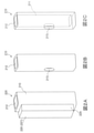
図2A~Cは、実施の形態1に係る検出チップ200の構成を示す模式図である。図2Aは、検出チップ200の斜視図であり、図2Bは、ウェル本体210の斜視図であり、図2Cは、ウェル本体210の斜視透視図である。図3Aおよび図3Bは、検出チップ200に入射する光(励起光α)と検出チップ200から出射する光(蛍光βおよびプラズモン散乱光γ)を示す模式図である。図3Aは、検出チップ200の高さ方向に沿う断面図であり、図3Bは、検出チップ200の水平方向に沿う断面図である。図3Aおよび図3Bでは、収容部211内に液体(例えば測定用緩衝液)が収容されている状態を示している。図4は、図3Aの断面図における反応場226近傍を拡大した部分拡大断面図である。
(Detection chip)
2A to 2C are schematic views showing the configuration of the detection chip 200 according to the first embodiment. 2A is a perspective view of the detection chip 200, FIG. 2B is a perspective view of the well body 210, and FIG. 2C is a perspective perspective view of the well body 210. 3A and 3B are schematic views showing light incident on the detection chip 200 (excitation light α) and light emitted from the detection chip 200 (fluorescent β and plasmon scattered light γ). FIG. 3A is a cross-sectional view taken along the height direction of the detection chip 200, and FIG. 3B is a cross-sectional view taken along the horizontal direction of the detection chip 200. 3A and 3B show a state in which a liquid (for example, a buffer solution for measurement) is contained in the accommodating portion 211. FIG. 4 is a partially enlarged cross-sectional view of the vicinity of the reaction field 226 in the cross-sectional view of FIG. 3A.

図2A、図3Aおよび図3Bに示されるように、検出チップ200は、ウェル本体210および側壁部材220を有する。 As shown in FIGS. 2A, 3A and 3B, the detection tip 200 has a well body 210 and a side wall member 220.

ウェル本体210は、その内部に収容部(ウェル)211を有している。収容部211は、液体を収容できるように構成された有底の凹部であり、上部に設けられた第1開口212および側部に設けられた第2開口213により外部に開放されている。第1開口212は、収容部211内に液体を導入したり収容部211内の液体を除去したりする際に利用される。第2開口213は、この後説明する側壁部材220の捕捉領域227を収容部211内に露出させて反応場226を形成するために形成されている(図4参照)。第2開口213は、収容部211内に液体を収容できるように側壁部材220により閉塞される。本実施の形態では、図2Bおよび図2Cに示されるように、第2開口213は、収容部211を構成する4つの側壁のうちの側壁部材220側の側壁に形成された貫通孔である。 The well body 210 has an accommodating portion (well) 211 inside thereof. The accommodating portion 211 is a bottomed recess configured to accommodate a liquid, and is opened to the outside by a first opening 212 provided at the upper part and a second opening 213 provided at the side portion. The first opening 212 is used when introducing a liquid into the accommodating portion 211 or removing the liquid in the accommodating portion 211. The second opening 213 is formed to expose the capture region 227 of the side wall member 220, which will be described later, into the accommodating portion 211 to form the reaction field 226 (see FIG. 4). The second opening 213 is closed by the side wall member 220 so that the liquid can be accommodated in the accommodating portion 211. In the present embodiment, as shown in FIGS. 2B and 2C, the second opening 213 is a through hole formed in the side wall on the side wall member 220 side of the four side walls constituting the accommodating portion 211.

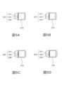
本実施の形態に係る検出チップ200では、反応場226近傍から放出された光(蛍光βおよびプラズモン散乱光γ)が、反応場226と対向する側壁を透過し、後述する検出部125により検出される(図1参照)。したがって、検出されるべき光の屈折を抑制したい場合は、図5Aに示されるように、収容部において反応場226(捕捉領域227)と対向する側壁の内面および外面は、いずれも平面であることが好ましい。一方、検出されるべき光を検出部125に向けて集めたい場合は、図5B~Dに示されるように、収容部において反応場226と対向する側壁の内面および外面の少なくとも一方は、凸曲面であることが好ましい。図5Bに示される例では、側壁の内面のみが凸曲面であり、反応場226と対向する側壁は平凸のシリンドリカルレンズとして機能する。図5Cに示される例では、側壁の外面のみが凸曲面であり、反応場226と対向する側壁は平凸のシリンドリカルレンズとして機能する。図5Dに示される例では、側壁の内面および外面がいずれも凸曲面であり、反応場226と対向する側壁は両凸のシリンドリカルレンズとして機能する。 In the detection chip 200 according to the present embodiment, the light (fluorescent β and plasmon scattered light γ) emitted from the vicinity of the reaction field 226 passes through the side wall facing the reaction field 226 and is detected by the detection unit 125 described later. (See Fig. 1). Therefore, if it is desired to suppress the refraction of light to be detected, as shown in FIG. 5A, the inner and outer surfaces of the side wall facing the reaction field 226 (capture area 227) in the accommodating portion must be both flat. Is preferable. On the other hand, if it is desired to collect the light to be detected toward the detection unit 125, as shown in FIGS. 5B to 5D, at least one of the inner surface and the outer surface of the side wall facing the reaction field 226 in the accommodation unit is a convex curved surface. Is preferable. In the example shown in FIG. 5B, only the inner surface of the side wall is a convex curved surface, and the side wall facing the reaction field 226 functions as a plano-convex cylindrical lens. In the example shown in FIG. 5C, only the outer surface of the side wall is a convex curved surface, and the side wall facing the reaction field 226 functions as a plano-convex cylindrical lens. In the example shown in FIG. 5D, both the inner and outer surfaces of the side wall are convex curved surfaces, and the side wall facing the reaction field 226 functions as a biconvex cylindrical lens.

ウェル本体210の形状は、収容部211、第1開口212および第2開口213を有していれば特に限定されない。図6Aは、第1変形例に係る検出チップ200の斜視図であり、図6Bは、第1変形例に係るウェル本体210の斜視図である。たとえば、図6Aおよび図6Bに示されるように、第2開口213は、側壁部材220側の全面に形成されていてもよく、第1開口212と繋がっていてもよい。この場合も、第2開口213の少なくとも一部は、収容部211内に液体を収容できるように側壁部材220により閉塞される。 The shape of the well body 210 is not particularly limited as long as it has the accommodating portion 211, the first opening 212, and the second opening 213. FIG. 6A is a perspective view of the detection chip 200 according to the first modification, and FIG. 6B is a perspective view of the well body 210 according to the first modification. For example, as shown in FIGS. 6A and 6B, the second opening 213 may be formed on the entire surface on the side wall member 220 side, or may be connected to the first opening 212. Also in this case, at least a part of the second opening 213 is closed by the side wall member 220 so that the liquid can be accommodated in the accommodating portion 211.

図7Aは、第2変形例に係るウェル本体210の斜視図であり、図7Bは、第2変形例に係るウェル本体210の水平方向に沿う断面図であり、図7Cは、第2変形例に係るウェル本体210の底部近傍の高さ方向に沿う断面図である。たとえば、図7Aに示されるように、ウェル本体210は、その上部から側方に突出する保持部214をさらに有していてもよい。このように検出チップ200が保持部214を有している場合、ユーザーおよびシステムは保持部を把持することができるため、検出チップ200の取扱いがより容易になる。また、図7Bに示されるように、収容部211を構成する4つの側壁のうちの、反応場227と対向する側壁以外の側壁の内面の全部または一部は、周方向に曲がった曲面であってもよい。このような構成とすることで、検出チップ200に周方向の回転振動を加えた場合に、収容部211内の液体を効率よく撹拌することができる。なお、検出チップ200に水平方向の往復振動を加える場合は、収容部211の水平方向に沿った断面形状は、略多角形状(例えば略正方形状)であることが好ましい(図3B参照)。また、図7Cに示されるように、収容部211の底部は、下に凸形状(例えば丸底)であってもよい。このような構成とすることで、収容部211内の液体をより確実に除去することが可能となり、検出精度を向上させることができる。 7A is a perspective view of the well body 210 according to the second modification, FIG. 7B is a cross-sectional view of the well body 210 according to the second modification along the horizontal direction, and FIG. 7C is a second modification. It is sectional drawing along the height direction near the bottom of the well main body 210 which concerns on. For example, as shown in FIG. 7A, the well body 210 may further have a holding portion 214 that projects laterally from above. When the detection chip 200 has the holding portion 214 in this way, the user and the system can grip the holding portion, so that the handling of the detection chip 200 becomes easier. Further, as shown in FIG. 7B, of the four side walls constituting the accommodating portion 211, all or a part of the inner surface of the side wall other than the side wall facing the reaction field 227 is a curved surface curved in the circumferential direction. You may. With such a configuration, when the detection chip 200 is subjected to rotational vibration in the circumferential direction, the liquid in the accommodating portion 211 can be efficiently agitated. When horizontal reciprocating vibration is applied to the detection chip 200, the cross-sectional shape of the accommodating portion 211 along the horizontal direction is preferably a substantially polygonal shape (for example, a substantially square shape) (see FIG. 3B). Further, as shown in FIG. 7C, the bottom portion of the accommodating portion 211 may have a downwardly convex shape (for example, a round bottom). With such a configuration, the liquid in the accommodating portion 211 can be removed more reliably, and the detection accuracy can be improved.

ウェル本体210は、光(少なくとも励起光αの波長の光および蛍光βの波長の光)に対して透明な材料で形成されている。ただし、後述の検出方法における光の取り出しの妨げにならない限り、ウェル本体210の一部は光に対して不透明な材料で形成されていてもよい。少なくとも、収容部211を構成する4つの側壁のうちの反応場226と対向する側壁は、光透過性を有している。光に対して透明な材料の例には、樹脂およびガラスが含まれる。 The well body 210 is made of a material that is transparent to light (at least light having a wavelength of excitation light α and light having a wavelength of fluorescence β). However, a part of the well body 210 may be made of a material opaque to light as long as it does not interfere with the extraction of light in the detection method described later. At least, of the four side walls constituting the accommodating portion 211, the side wall facing the reaction field 226 has light transmission. Examples of materials that are transparent to light include resins and glass.

側壁部材220は、光学素子としてのプリズム221、金属膜225および反応場226を有している。ここで「反応場」とは、金属膜225上に配置された捕捉領域227のうち、第2開口213を介して収容部211内に露出している領域を意味する(図4参照)。図2A、図3A、図3Bおよび図4に示されるように、側壁部材220は、捕捉領域227の少なくとも一部が収容部211内に露出して反応場226となり、かつ側壁部材220が第2開口213の少なくとも一部を完全に閉塞するようにウェル本体210に固定されている。本実施の形態では、側壁部材220は、第2開口213の全部を閉塞するように、両面テープなどの接着層(図示せず)を介してウェル本体210に接着されている。側壁部材220は、接着層を用いずに、レーザー溶着、超音波溶着、クランプ部材を用いた圧着などにより、ウェル本体210に接合されていてもよい。 The side wall member 220 has a prism 221 as an optical element, a metal film 225, and a reaction field 226. Here, the “reaction field” means a region of the capture region 227 arranged on the metal film 225 that is exposed in the accommodating portion 211 via the second opening 213 (see FIG. 4). As shown in FIGS. 2A, 3A, 3B and 4, in the side wall member 220, at least a part of the capture region 227 is exposed in the accommodating portion 211 to become a reaction field 226, and the side wall member 220 is the second. It is fixed to the well body 210 so as to completely close at least a part of the opening 213. In the present embodiment, the side wall member 220 is adhered to the well body 210 via an adhesive layer (not shown) such as double-sided tape so as to close the entire second opening 213. The side wall member 220 may be joined to the well body 210 by laser welding, ultrasonic welding, crimping using a clamp member, or the like without using an adhesive layer.

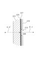
プリズム221は、励起光αに対して透明な誘電体からなる光学素子であり、図3Bに示されるように、入射面222、反射面223および出射面224を有する。プリズム221は、収容部211を構成する側壁としても機能する。入射面222は、励起光照射ユニット110からの励起光αをプリズム221の内部に入射させるための面である。プリズム221の内部に入射した励起光αは、反射面223で反射する。この後説明するように、反射面223上には金属膜225および捕捉領域227が順に配置されている。出射面224は、反射面223で反射した反射光α’をプリズム221の外部に出射させるための面である。 The prism 221 is an optical element made of a dielectric material transparent to the excitation light α, and has an entrance surface 222, a reflection surface 223, and an emission surface 224 as shown in FIG. 3B. The prism 221 also functions as a side wall constituting the accommodating portion 211. The incident surface 222 is a surface for incident the excitation light α from the excitation light irradiation unit 110 into the inside of the prism 221. The excitation light α incident on the inside of the prism 221 is reflected by the reflection surface 223. As will be described later, the metal film 225 and the capture region 227 are sequentially arranged on the reflection surface 223. The emission surface 224 is a surface for emitting the reflected light α'reflected by the reflection surface 223 to the outside of the prism 221.

プリズム221の形状は特に限定されないが、反射面223は平面であることが好ましい。プリズム221の形状の例には、台形を底面とする柱体、三角柱、半円柱が含まれる。本実施の形態では、プリズム221の形状は、台形を底面とする柱体である。台形の一方の底辺に対応する面が反射面223であり、一方の脚に対応する面が入射面222であり、他方の脚に対応する面が出射面224である。 The shape of the prism 221 is not particularly limited, but the reflecting surface 223 is preferably a flat surface. Examples of the shape of the prism 221 include a prism having a trapezoidal bottom surface, a triangular prism, and a semi-cylinder. In the present embodiment, the shape of the prism 221 is a prism whose bottom surface is a trapezoid. The surface corresponding to one bottom of the trapezoid is the reflective surface 223, the surface corresponding to one leg is the incident surface 222, and the surface corresponding to the other leg is the exit surface 224.

入射面222は、励起光αが励起光照射ユニット110に戻らないように形成される。励起光αの光源がレーザーダイオード(以下「LD」ともいう)である場合、励起光αがLDに戻ると、LDの励起状態が乱れてしまい、励起光αの波長や出力が変動してしまう。そこで、理想的な共鳴角または増強角を中心とする走査範囲において、励起光αが入射面222に垂直に入射しないように、入射面222の角度が設定される。ここで「共鳴角」とは、反射面223(金属膜225)に対する励起光αの入射角を走査した場合に、出射面224から出射される反射光α’の光量が最小となるときの、入射角を意味する。また、「増強角」とは、反射面223(金属膜225)に対する励起光αの入射角を走査した場合に、反応場226周辺から収容部211内に放出される励起光αと同一波長の散乱光(プラズモン散乱光)γの光量が最大となるときの、入射角を意味する。本実施の形態では、入射面222と反射面223との角度および反射面223と出射面224との角度は、いずれも約80°である。 The incident surface 222 is formed so that the excitation light α does not return to the excitation light irradiation unit 110. When the light source of the excitation light α is a laser diode (hereinafter, also referred to as “LD”), when the excitation light α returns to the LD, the excited state of the LD is disturbed and the wavelength and output of the excitation light α fluctuate. .. Therefore, the angle of the incident surface 222 is set so that the excitation light α is not incident perpendicularly to the incident surface 222 in the scanning range centered on the ideal resonance angle or augmentation angle. Here, the "resonance angle" means that when the incident angle of the excitation light α with respect to the reflection surface 223 (metal film 225) is scanned, the amount of the reflected light α'emitted from the emission surface 224 is minimized. It means the angle of incidence. Further, the “enhanced angle” is the same wavelength as the excitation light α emitted from the periphery of the reaction field 226 into the accommodating portion 211 when the incident angle of the excitation light α with respect to the reflection surface 223 (metal film 225) is scanned. Scattered light (Plazmon scattered light) It means the incident angle when the amount of light of γ is maximum. In the present embodiment, the angle between the incident surface 222 and the reflecting surface 223 and the angle between the reflecting surface 223 and the emitting surface 224 are both about 80 °.

なお、検出チップ200の設計により、共鳴角(およびその極近傍にある増強角)が概ね決まる。設計要素は、プリズム221の屈折率や、金属膜225の屈折率、金属膜225の膜厚、金属膜225の消衰係数、励起光αの波長などである。金属膜225上の反応場226(捕捉領域227)に捕捉された被検出物質によって共鳴角および増強角がシフトするが、その量は数度未満である。 The resonance angle (and the augmented angle in the immediate vicinity thereof) is largely determined by the design of the detection chip 200. The design elements include the refractive index of the prism 221, the refractive index of the metal film 225, the film thickness of the metal film 225, the extinction coefficient of the metal film 225, the wavelength of the excitation light α, and the like. The substance to be detected that is captured in the reaction field 226 (capture region 227) on the metal film 225 shifts the resonance angle and the enhancement angle, but the amount is less than a few degrees.

プリズム221は、複屈折特性を少なからず有する。プリズム221の材料の例には、樹脂およびガラスが含まれる。プリズム221の材料は、好ましくは、屈折率が1.4~1.6であり、かつ複屈折が小さい樹脂である。 The prism 221 has not a little birefringence characteristic. Examples of materials for prism 221 include resin and glass. The material of the prism 221 is preferably a resin having a refractive index of 1.4 to 1.6 and a small birefringence.

金属膜225は、プリズム221の反射面223上に配置されている。これにより、反射面223に全反射条件で入射した励起光αの光子と、金属膜225中の自由電子との間で相互作用(SPR)が生じ、金属膜225の表面上に局在する増強電場が生じる。 The metal film 225 is arranged on the reflecting surface 223 of the prism 221. As a result, an interaction (SPR) occurs between the photons of the excited light α incident on the reflecting surface 223 under total reflection conditions and the free electrons in the metal film 225, and the enhancement localized on the surface of the metal film 225. An electric field is generated.

金属膜225の材料は、表面プラズモン共鳴を生じさせうる金属であれば特に限定されない。金属膜225の材料の例には、金、銀、銅、アルミニウムおよびこれらの合金が含まれる。金属膜225の形成方法は、特に限定されない。金属膜225の形成方法の例には、スパッタリング、蒸着、めっきが含まれる。金属膜225の厚みは、特に限定されないが、30~70nmの範囲内であることが好ましい。 The material of the metal film 225 is not particularly limited as long as it is a metal capable of causing surface plasmon resonance. Examples of materials for the metal film 225 include gold, silver, copper, aluminum and alloys thereof. The method for forming the metal film 225 is not particularly limited. Examples of methods for forming the metal film 225 include sputtering, vapor deposition, and plating. The thickness of the metal film 225 is not particularly limited, but is preferably in the range of 30 to 70 nm.

反応場226は、収容部211内に露出している、被検出物質を捕捉するための領域である。前述のとおり、反応場226は、金属膜225上に配置された捕捉領域227のうち、第2開口213を介して収容部211内に露出している領域を意味する。図4に示されるように、捕捉領域227の大きさが第2開口213を閉塞することが可能な大きさである場合、反応場226の範囲は、第2開口213により規定される。このような構成とすることで、反応場226の大きさを高精度かつ容易に調整することが可能となる。一方、図6Bに示されるように、第2開口213の大きさが(捕捉領域227よりも)大きい場合は、金属膜225の表面の一部に所定形状の捕捉領域227が形成され、この捕捉領域227がそのまま反応場226となる。 The reaction field 226 is an area for capturing the substance to be detected, which is exposed in the accommodating portion 211. As described above, the reaction field 226 means a region of the capture region 227 arranged on the metal film 225 that is exposed in the accommodating portion 211 via the second opening 213. As shown in FIG. 4, when the size of the capture region 227 is large enough to block the second opening 213, the range of the reaction field 226 is defined by the second opening 213. With such a configuration, the size of the reaction field 226 can be easily adjusted with high accuracy. On the other hand, as shown in FIG. 6B, when the size of the second opening 213 is larger (than the capture region 227), a capture region 227 having a predetermined shape is formed on a part of the surface of the metal film 225, and the capture region 227 has a predetermined shape. The region 227 becomes the reaction field 226 as it is.

反応場226は、収容部211の内側面に配置される。このとき、反応場226は、収容部211の最深部から離れた位置に配置されることが好ましい。このような構成とすることで、収容部211内に検体などを導入したときに反応場226において効率よく反応を生じさせることができる。また、蛍光βの検出時に、収容部211の底部に起因するノイズが検出結果に混じることを抑制することもできる。 The reaction field 226 is arranged on the inner surface of the accommodating portion 211. At this time, it is preferable that the reaction field 226 is arranged at a position away from the deepest portion of the accommodating portion 211. With such a configuration, when a sample or the like is introduced into the accommodating portion 211, a reaction can be efficiently generated in the reaction field 226. Further, when the fluorescent β is detected, it is possible to suppress the noise caused by the bottom of the accommodating portion 211 from being mixed with the detection result.

捕捉領域227は、金属膜225上において被検出物質を捕捉するための第1の捕捉体が固定化されている領域である。第1の捕捉体は、検体中の被検出物質と特異的に結合するための認識部位を有する物質である。反応場226(捕捉領域227)に第1の捕捉体が固定されていると、収容部211内に検体を導入したときに、第1の捕捉体に被検出物質が選択的に結合する。つまり、被検出物質が反応場226に捕捉される。これにより、後述のように被検出物質を検出することが可能となる。第1の捕捉体の種類は、被検出物質に特異的に結合するための認識部位を有していれば特に制限されない。第1の捕捉体の例には、被検出物質に特異的に結合可能な抗体(1次抗体)またはその断片、被検出物質に特異的に結合可能な酵素などが含まれる。 The capture region 227 is a region on the metal film 225 on which the first capture body for capturing the detected substance is immobilized. The first trap is a substance having a recognition site for specifically binding to the substance to be detected in the sample. When the first trap is fixed in the reaction field 226 (capture area 227), the substance to be detected selectively binds to the first trap when the sample is introduced into the accommodating portion 211. That is, the substance to be detected is captured in the reaction field 226. This makes it possible to detect the substance to be detected as described later. The type of the first trap is not particularly limited as long as it has a recognition site for specifically binding to the substance to be detected. Examples of the first trap include an antibody (primary antibody) or a fragment thereof that can specifically bind to the substance to be detected, an enzyme that can specifically bind to the substance to be detected, and the like.

検出精度を向上させる観点からは、反応場226となる領域において捕捉領域227が配置されている面は、平面であることが好ましい。すなわち、本実施の形態のように捕捉領域227が金属膜225上に配置されている場合は、金属膜225の表面は平面であることが好ましい。また、本実施の形態の最後に説明するように、捕捉領域227が反射面223上に配置されている場合は、反射面223は平面であることが好ましい。 From the viewpoint of improving the detection accuracy, it is preferable that the surface on which the capture region 227 is arranged in the region serving as the reaction field 226 is a flat surface. That is, when the capture region 227 is arranged on the metal film 225 as in the present embodiment, it is preferable that the surface of the metal film 225 is flat. Further, as described at the end of the present embodiment, when the capture region 227 is arranged on the reflection surface 223, it is preferable that the reflection surface 223 is a flat surface.

なお、図8A~Cに示されるように、検出チップ200は、収容部211以外にも液体を収容可能な第2収容部230をさらに有していてもよい。第2収容部230の用途は、特に限定されない。たとえば、第2収容部230に、反応工程または検出工程で使用される試薬をあらかじめ収容しておいてもよい。また、反応工程または検出工程において、第2収容部230で2種以上の試薬を混合してもよい。第2収容部230の数および位置は、被検出物質の検出の妨げとならなければ特に限定されない。たとえば、図8Aに示されるように、収容部211を構成する4つの側壁のうちの側壁部材220側の側壁に1つの第2収容部230を付加してもよい。また、図8Bに示されるように、収容部211を構成する4つの側壁のうちの反応場226と対向する側壁に1つの第2収容部230を付加してもよい。また、図8Cに示されるように、収容部211を構成する4つの側壁のうちの1つの側壁に複数の第2収容部230を付加してもよい。これらの図に示されるように、収容部211を構成する4つの側壁のうちの側壁部材220側の側壁または反応場226と対向する側壁に第2収容部230を付加した場合、検出チップ200の平面視形状は略長方形となり、複数の検出チップ200を収納容器内に効率よく収容することができる。 As shown in FIGS. 8A to 8C, the detection chip 200 may further have a second accommodating portion 230 capable of accommodating the liquid in addition to the accommodating portion 211. The use of the second accommodating portion 230 is not particularly limited. For example, the reagent used in the reaction step or the detection step may be stored in advance in the second storage unit 230. Further, in the reaction step or the detection step, two or more kinds of reagents may be mixed in the second storage unit 230. The number and position of the second accommodating portion 230 are not particularly limited as long as they do not interfere with the detection of the substance to be detected. For example, as shown in FIG. 8A, one second accommodating portion 230 may be added to the side wall on the side wall member 220 side of the four side walls constituting the accommodating portion 211. Further, as shown in FIG. 8B, one second accommodating portion 230 may be added to the side wall facing the reaction field 226 among the four side walls constituting the accommodating portion 211. Further, as shown in FIG. 8C, a plurality of second accommodating portions 230 may be added to one side wall of the four side walls constituting the accommodating portion 211. As shown in these figures, when the second accommodating portion 230 is added to the side wall on the side wall member 220 side of the four side walls constituting the accommodating portion 211 or the side wall facing the reaction field 226, the detection chip 200 The plan view shape is substantially rectangular, and a plurality of detection chips 200 can be efficiently housed in the storage container.

(検出システム)
次に、検出システム100の検出チップ200以外の構成要素について説明する。前述のとおり、検出システム100は、検出チップ200以外に、励起光照射ユニット110、蛍光検出ユニット120、送液ユニット130、加振部140、および制御部150を有する(図1参照)。
(Detection system)
Next, components other than the detection chip 200 of the detection system 100 will be described. As described above, the detection system 100 includes an excitation light irradiation unit 110, a fluorescence detection unit 120, a liquid feed unit 130, a vibration vibration unit 140, and a control unit 150 in addition to the detection chip 200 (see FIG. 1).

励起光照射ユニット110は、検出チップ200に励起光αを照射する。蛍光βまたはプラズモン散乱光γの測定時には、励起光照射ユニット110は、プリズム221の反射面223(金属膜225)に対する入射角が金属膜225でSPRを生じさせる角度となるように、反射面223(金属膜225)に対するP波のみをプリズム221の入射面222に向けて出射する。ここで「励起光」とは、蛍光物質を直接または間接的に励起させる光である。たとえば、励起光αは、プリズム221を介して反射面223(金属膜225)に金属膜225でSPRが生じる角度で照射されたときに、蛍光物質を励起させる増強電場を金属膜225の表面上に生じさせる光である。励起光照射ユニット110は、光源ユニット111および第1角度調整部112を含む。 The excitation light irradiation unit 110 irradiates the detection chip 200 with the excitation light α. At the time of measuring fluorescent β or plasmon scattered light γ, the excitation light irradiation unit 110 has a reflecting surface 223 so that the incident angle of the prism 221 with respect to the reflecting surface 223 (metal film 225) is an angle that causes SPR in the metal film 225. Only the P wave with respect to (metal film 225) is emitted toward the incident surface 222 of the prism 221. Here, the "excitation light" is light that directly or indirectly excites a fluorescent substance. For example, the excitation light α applies an enhanced electric field that excites a fluorescent substance on the surface of the metal film 225 when the reflective surface 223 (metal film 225) is irradiated with the reflecting surface 223 (metal film 225) via the prism 221 at an angle at which SPR is generated by the metal film 225. It is the light that is generated in. The excitation light irradiation unit 110 includes a light source unit 111 and a first angle adjusting unit 112.

光源ユニット111は、コリメートされ、かつ波長および光量が一定の励起光αを、反射面223(金属膜225の表面)における照射スポットの形状が略円形となるように出射する。照射スポットの大きさは、検出チップ200の反応場226よりも小さいことが好ましい。光源ユニット111は、例えば、励起光αの光源、ビーム整形光学系、APC機構および温度調整機構(いずれも不図示)を含む。 The light source unit 111 emits excitation light α that is collimated and has a constant wavelength and light amount so that the shape of the irradiation spot on the reflection surface 223 (the surface of the metal film 225) is substantially circular. The size of the irradiation spot is preferably smaller than the reaction field 226 of the detection chip 200. The light source unit 111 includes, for example, a light source for excitation light α, a beam shaping optical system, an APC mechanism, and a temperature adjusting mechanism (all not shown).

光源の種類は、特に限定されず、例えばレーザーダイオード(LD)である。光源の他の例には、発光ダイオード、水銀灯、その他のレーザー光源が含まれる。光源から出射される光がビームでない場合は、光源から出射される光は、レンズや鏡、スリットなどによりビームに変換される。また、光源から出射される光が単色光でない場合は、光源から出射される光は、回折格子などにより単色光に変換される。さらに、光源から出射される光が直線偏光でない場合は、光源から出射される光は、偏光子などにより直線偏光の光に変換される。 The type of the light source is not particularly limited, and is, for example, a laser diode (LD). Other examples of light sources include light emitting diodes, mercury lamps, and other laser light sources. When the light emitted from the light source is not a beam, the light emitted from the light source is converted into a beam by a lens, a mirror, a slit, or the like. When the light emitted from the light source is not monochromatic light, the light emitted from the light source is converted into monochromatic light by a diffraction grating or the like. Further, when the light emitted from the light source is not linearly polarized light, the light emitted from the light source is converted into linearly polarized light by a splitter or the like.

ビーム整形光学系は、例えば、コリメーターやバンドパスフィルター、直線偏光フィルター、半波長板、スリット、ズーム手段などを含む。ビーム整形光学系は、これらのすべてを含んでいてもよいし、一部を含んでいてもよい。コリメーターは、光源から出射された励起光αをコリメートする。バンドパスフィルターは、光源から出射された励起光αを中心波長のみの狭帯域光にする。光源からの励起光αは、若干の波長分布幅を有しているためである。直線偏光フィルターは、光源から出射された励起光αを完全な直線偏光の光にする。半波長板は、反射面223にP波成分が入射するように励起光αの偏光方向を調整する。スリットおよびズーム手段は、反射面223における照射スポットの形状が所定サイズの円形となるように、励起光αのビーム径や輪郭形状などを調整する。 The beam shaping optical system includes, for example, a collimator, a bandpass filter, a linear polarizing filter, a half-wave plate, a slit, a zoom means, and the like. The beam shaping optical system may include all of these, or may include some of them. The collimator collimates the excitation light α emitted from the light source. The bandpass filter converts the excitation light α emitted from the light source into narrow-band light having only a central wavelength. This is because the excitation light α from the light source has a slight wavelength distribution width. The linear polarization filter makes the excitation light α emitted from the light source completely linearly polarized light. The half-wave plate adjusts the polarization direction of the excitation light α so that the P wave component is incident on the reflection surface 223. The slit and the zoom means adjust the beam diameter, contour shape, and the like of the excitation light α so that the shape of the irradiation spot on the reflection surface 223 is a circle of a predetermined size.

APC機構は、光源の出力が一定となるように光源を制御する。より具体的には、APC機構は、励起光αから分岐させた光の光量を不図示のフォトダイオードなどで検出する。そして、APC機構は、回帰回路で投入エネルギーを制御することで、光源の出力を一定に制御する。 The APC mechanism controls the light source so that the output of the light source is constant. More specifically, the APC mechanism detects the amount of light branched from the excitation light α with a photodiode (not shown) or the like. Then, the APC mechanism controls the output of the light source to be constant by controlling the input energy with the regression circuit.

温度調整機構は、例えば、ヒーターやペルチェ素子などである。光源の出射光の波長およびエネルギーは、温度によって変動することがある。このため、温度調整機構で光源の温度を一定に保つことにより、光源の出射光の波長およびエネルギーを一定に制御する。 The temperature control mechanism is, for example, a heater or a Pelche element. The wavelength and energy of the emitted light from the light source may vary with temperature. Therefore, the wavelength and energy of the emitted light of the light source are controlled to be constant by keeping the temperature of the light source constant by the temperature adjusting mechanism.

第1角度調整部112は、反射面223に対する励起光αの入射角を調整する。第1角度調整部112は、プリズム221を介して反射面223の所定の位置に向けて所定の入射角で励起光αを照射するために、励起光αの光軸と検出チップ200とを相対的に回転させる。 The first angle adjusting unit 112 adjusts the incident angle of the excitation light α with respect to the reflecting surface 223. The first angle adjusting unit 112 makes the optical axis of the excitation light α and the detection chip 200 relative to each other in order to irradiate the excitation light α at a predetermined incident angle toward a predetermined position of the reflection surface 223 via the prism 221. Rotate.

たとえば、第1角度調整部112は、光源ユニット111を励起光αの光軸と直交する軸(検出チップ200の高さ方向に沿う軸)を中心として回動させる(図3B参照)。このとき、入射角を走査しても反射面223での照射スポットの位置がほとんど変化しないように、回転軸の位置を設定する。 For example, the first angle adjusting unit 112 rotates the light source unit 111 about an axis orthogonal to the optical axis of the excitation light α (an axis along the height direction of the detection chip 200) (see FIG. 3B). At this time, the position of the rotation axis is set so that the position of the irradiation spot on the reflection surface 223 hardly changes even if the incident angle is scanned.

前述のとおり、反射面223(金属膜225)に対する励起光αの入射角のうち、プラズモン散乱光γの光量が最大となる角度が増強角である。励起光αの入射角を増強角またはその近傍の角度(例えば共鳴角)に設定することで、高強度の蛍光βを測定することが可能となる。検出チップ200のプリズム221の材料および形状、金属膜225の膜厚、収容部211内の液体の屈折率などにより、励起光αの基本的な入射条件が決まるが、使用する蛍光物質の種類および量、プリズム221の形状誤差などにより、最適な入射条件はわずかに変動する。このため、検出ごとに最適な増強角を求めることが好ましい。 As described above, among the angles of incidence of the excitation light α on the reflection surface 223 (metal film 225), the angle at which the amount of plasmon scattered light γ is maximized is the enhancement angle. By setting the incident angle of the excitation light α to an angle at or near the augmented angle (for example, a resonance angle), it is possible to measure high-intensity fluorescence β. The basic incident conditions of the excitation light α are determined by the material and shape of the prism 221 of the detection chip 200, the film thickness of the metal film 225, the refractive index of the liquid in the accommodating portion 211, etc. The optimum incident conditions vary slightly depending on the amount, the shape error of the prism 221 and the like. Therefore, it is preferable to obtain the optimum enhancement angle for each detection.

蛍光検出ユニット120は、反射面223(金属膜225)への励起光αの照射によって生じた蛍光βを検出する。また、必要に応じて、蛍光検出ユニット120は、反射面223(金属膜225)への励起光αの照射によって生じたプラズモン散乱光γも検出する。蛍光検出ユニット120は、第1レンズ121、光学フィルター122、第2レンズ123、位置切替部124および検出部125を含む。 The fluorescence detection unit 120 detects the fluorescence β generated by irradiating the reflective surface 223 (metal film 225) with the excitation light α. If necessary, the fluorescence detection unit 120 also detects the plasmon scattered light γ generated by irradiating the reflective surface 223 (metal film 225) with the excitation light α. The fluorescence detection unit 120 includes a first lens 121, an optical filter 122, a second lens 123, a position switching unit 124, and a detection unit 125.

第1レンズ121は、例えば、集光レンズであり、反応場226近傍から出射される光を集光する。第2レンズ123は、例えば、結像レンズであり、第1レンズ121で集光された光を検出部125の受光面に結像させる。両レンズの間の光路は、略平行な光路になっている。光学フィルター122は、両レンズの間に配置されている。 The first lens 121 is, for example, a condensing lens, and condenses light emitted from the vicinity of the reaction field 226. The second lens 123 is, for example, an imaging lens, and the light collected by the first lens 121 is imaged on the light receiving surface of the detection unit 125. The optical path between the two lenses is a substantially parallel optical path. The optical filter 122 is arranged between both lenses.

光学フィルター122は、蛍光成分のみを検出部125に導き、高いS(シグナル)/N(ノイズ)比で蛍光βを検出するために、励起光成分(プラズモン散乱光γ)を除去する。光学フィルター122の例には、励起光反射フィルター、短波長カットフィルターおよびバンドパスフィルターが含まれる。光学フィルター122は、例えば、所定の光成分を反射する多層膜を含むフィルター、または所定の光成分を吸収する色ガラスフィルターである。 The optical filter 122 guides only the fluorescent component to the detection unit 125, and removes the excitation light component (plasmon scattered light γ) in order to detect the fluorescent β with a high S (signal) / N (noise) ratio. Examples of the optical filter 122 include an excitation light reflection filter, a short wavelength cut filter and a bandpass filter. The optical filter 122 is, for example, a filter including a multilayer film that reflects a predetermined light component, or a colored glass filter that absorbs a predetermined light component.

位置切替部124は、光学フィルター122の位置を、第1レンズ121および第2レンズ123間の光路上または光路外に切り替える。具体的には、検出部125が蛍光βを検出する時には、光学フィルター122を光路上に配置し、検出部125がプラズモン散乱光γを検出する時には、光学フィルター122を光路外に配置する。 The position switching unit 124 switches the position of the optical filter 122 on or out of the optical path between the first lens 121 and the second lens 123. Specifically, when the detection unit 125 detects the fluorescent β, the optical filter 122 is arranged on the optical path, and when the detection unit 125 detects the plasmon scattered light γ, the optical filter 122 is arranged outside the optical path.

検出部125は、蛍光βおよびプラズモン散乱光γを検出する受光センサーである。検出部125は、微小量の被検出物質からの微弱な蛍光βを検出することが可能な、高い感度を有する。検出部125は、例えば、光電子増倍管(PMT)やアバランシェフォトダイオード(APD)などである。 The detection unit 125 is a light receiving sensor that detects fluorescent β and plasmon scattered light γ. The detection unit 125 has high sensitivity capable of detecting weak fluorescence β from a minute amount of the substance to be detected. The detection unit 125 is, for example, a photomultiplier tube (PMT), an avalanche photodiode (APD), or the like.

図1および図3Aに示されるように、本実施の形態では、光源ユニット111からの励起光αは水平方向に進行して、検出チップ200に到達する。また、反応場226近傍から放出され、水平方向に進行した光(蛍光βおよびプラズモン散乱光γ)が検出部125により検出される。したがって、本実施の形態では、光源ユニット111および検出部125は、検出チップ200と同じ高さに配置されている。もちろん、ミラーなどを用いれば光源ユニット111および検出部125の位置は自由に変更可能であるが、小型化の観点からは、光源ユニット111および検出部125は、検出チップ200と同じ高さに配置されていることが好ましい。 As shown in FIGS. 1 and 3A, in the present embodiment, the excitation light α from the light source unit 111 travels in the horizontal direction and reaches the detection chip 200. Further, the light emitted from the vicinity of the reaction field 226 and traveling in the horizontal direction (fluorescent β and plasmon scattered light γ) is detected by the detection unit 125. Therefore, in the present embodiment, the light source unit 111 and the detection unit 125 are arranged at the same height as the detection chip 200. Of course, the positions of the light source unit 111 and the detection unit 125 can be freely changed by using a mirror or the like, but from the viewpoint of miniaturization, the light source unit 111 and the detection unit 125 are arranged at the same height as the detection chip 200. It is preferable that it is.

送液ユニット130は、検出チップ200の収容部211内に各種液体を導入する。また、送液ユニット130は、検出チップ200の収容部211内から各種液体を除去する。本実施の形態では、送液ユニット130は、例えば検体や、蛍光物質で標識された第2の捕捉体を含む標識液(以下「標識液」ともいう)、洗浄液、測定用緩衝液などの注入および吸引を行う。送液ユニット130は、液体チップ131、ピペット132およびピペット制御部136を含む。 The liquid feeding unit 130 introduces various liquids into the accommodating portion 211 of the detection chip 200. Further, the liquid feeding unit 130 removes various liquids from the inside of the accommodating portion 211 of the detection chip 200. In the present embodiment, the liquid feeding unit 130 injects, for example, a sample, a labeling liquid containing a second trap labeled with a fluorescent substance (hereinafter, also referred to as “labeling liquid”), a cleaning liquid, a buffer solution for measurement, or the like. And perform suction. The liquid feeding unit 130 includes a liquid tip 131, a pipette 132, and a pipette control unit 136.

液体チップ131は、検体や標識液、洗浄液、測定用緩衝液などの液体をそれぞれ収容するための容器である。液体チップ131としては、通常、複数の容器が液体の種類に応じて配置されるか、または複数の容器が一体化したチップが配置される。なお、図8A~Cに示されるように、検出チップ200が第2収容部230を有している場合は、第2収容部230は液体チップ131として機能しうる。この場合は、送液ユニット130は、液体チップ131を有していなくてもよい。 The liquid chip 131 is a container for accommodating liquids such as a sample, a labeling liquid, a cleaning liquid, and a buffer solution for measurement. As the liquid chip 131, a plurality of containers are usually arranged according to the type of liquid, or a chip in which a plurality of containers are integrated is arranged. As shown in FIGS. 8A to 8C, when the detection chip 200 has the second accommodating portion 230, the second accommodating portion 230 can function as the liquid chip 131. In this case, the liquid feeding unit 130 does not have to have the liquid tip 131.

ピペット132は、シリンジポンプ133と、シリンジポンプ133に接続されたノズルユニット134と、ノズルユニット134の先端に装着されたピペットチップ135とを有する。シリンジポンプ133内のプランジャーの往復運動によって、ピペットチップ135における液体の吸引および排出が定量的に行われる。 The pipette 132 has a syringe pump 133, a nozzle unit 134 connected to the syringe pump 133, and a pipette tip 135 attached to the tip of the nozzle unit 134. The reciprocating motion of the plunger in the syringe pump 133 quantitatively sucks and drains the liquid in the pipette tip 135.

ピペット制御部136は、シリンジポンプ133の駆動装置、およびノズルユニット134の移動装置を含む。シリンジポンプ133の駆動装置は、シリンジポンプ133のプランジャーを往復運動させるための装置であり、例えば、ステッピングモーターを含む。ノズルユニット134の移動装置は、例えば、ノズルユニット134を、垂直方向と水平方向との二方向に自在に動かす。ノズルユニット134の移動装置は、例えば、ロボットアーム、2軸ステージまたは上下動自在なターンテーブルによって構成される。 The pipette control unit 136 includes a driving device for the syringe pump 133 and a moving device for the nozzle unit 134. The drive device for the syringe pump 133 is a device for reciprocating the plunger of the syringe pump 133, and includes, for example, a stepping motor. The moving device of the nozzle unit 134, for example, freely moves the nozzle unit 134 in two directions, a vertical direction and a horizontal direction. The moving device of the nozzle unit 134 is composed of, for example, a robot arm, a two-axis stage, or a vertically movable turntable.

ピペット制御部136は、シリンジポンプ133を駆動して、液体チップ131から各種液体をピペットチップ135内に吸引させる。そして、ピペット制御部136は、ノズルユニット134を移動させて、検出チップ200の収容部211内に第1開口212からピペットチップ135を挿入させるとともに、シリンジポンプ133を駆動して、ピペットチップ135内の液体を収容部211内に注入させる。また、液体の導入後、ピペット制御部136は、シリンジポンプ133を駆動して、収容部211内の液体をピペットチップ135内に吸引させる。このように収容部211内の液体を順次交換することによって、反応場226において第1の捕捉体と被検出物質を反応させたり(1次反応)、被検出物質と蛍光物質で標識された第2の捕捉体とを反応させたりする(2次反応)。 The pipette control unit 136 drives the syringe pump 133 to suck various liquids from the liquid tip 131 into the pipette tip 135. Then, the pipette control unit 136 moves the nozzle unit 134 to insert the pipette tip 135 into the accommodating unit 211 of the detection tip 200 from the first opening 212, and drives the syringe pump 133 to enter the pipette tip 135. Liquid is injected into the accommodating portion 211. Further, after the introduction of the liquid, the pipette control unit 136 drives the syringe pump 133 to suck the liquid in the accommodating unit 211 into the pipette tip 135. By sequentially exchanging the liquids in the accommodating portion 211 in this way, the first trapped substance and the detected substance are reacted in the reaction field 226 (primary reaction), or the detected substance is labeled with the fluorescent substance. It reacts with the capture body of 2 (secondary reaction).

加振部140は、収容部211内の液体を撹拌するために検出チップ200を振動させる。このように検出チップ200を振動させて収容部211内の液体を撹拌することで、反応場226における1次反応や2次反応、洗浄などを効率的に行うことができる。加振部140は、例えばピエゾ素子や偏芯させた回転体などである。加振部140は、励起光α、蛍光βおよびプラズモン散乱光γの光路を妨げない位置に配置される。 The vibrating unit 140 vibrates the detection chip 200 in order to agitate the liquid in the accommodating unit 211. By vibrating the detection chip 200 in this way and stirring the liquid in the accommodating portion 211, the primary reaction, the secondary reaction, washing, and the like in the reaction field 226 can be efficiently performed. The vibrating unit 140 is, for example, a piezo element, an eccentric rotating body, or the like. The excitation unit 140 is arranged at a position that does not obstruct the optical path of the excitation light α, the fluorescence β, and the plasmon scattered light γ.

加振部140により検出チップ200に加えられる振動の方向は、特に限定されない。振動方向の例には、水平方向や垂直方向(高さ方向)、周方向などが挙げられる。たとえば、加振部140としてのピエゾ素子を検出チップ200の側面に接触させた状態でピエゾ素子を駆動することで、検出チップ200に水平方向の往復振動を加えることができる。また、加振部140としてピエゾ素子を検出チップ200の底面に接触させた状態でピエゾ素子を駆動することで、検出チップ200に垂直方向の往復振動を加えることができる。また、加振部140としての偏芯させた回転体を検出チップ200の底面に接触させた状態で回転体を回転させることで、検出チップ200に周方向の回転振動を加えることができる。収容部211内の液体を効率よく撹拌する観点からは、収容部211内に液体が収容されている状態の検出チップ200の固有振動数、またはその前後の振動周波数で検出チップ200を振動させることが好ましい。また、異なる固有振動数(n次の固有振動数およびm次の固有振動数、nおよびmは正の整数)を順次切り替えながら検出チップ200を振動させてもよい。 The direction of vibration applied to the detection chip 200 by the vibrating unit 140 is not particularly limited. Examples of the vibration direction include a horizontal direction, a vertical direction (height direction), a circumferential direction, and the like. For example, by driving the piezo element in a state where the piezo element as the vibrating portion 140 is in contact with the side surface of the detection chip 200, horizontal reciprocating vibration can be applied to the detection chip 200. Further, by driving the piezo element in a state where the piezo element is in contact with the bottom surface of the detection chip 200 as the vibration boosting unit 140, it is possible to apply vertical reciprocating vibration to the detection chip 200. Further, by rotating the rotating body in a state where the eccentric rotating body as the vibrating portion 140 is in contact with the bottom surface of the detection chip 200, rotational vibration in the circumferential direction can be applied to the detection chip 200. From the viewpoint of efficiently stirring the liquid in the accommodating portion 211, the detection chip 200 is vibrated at the natural frequency of the detection chip 200 in a state where the liquid is accommodating in the accommodating portion 211, or at a vibration frequency before and after that. Is preferable. Further, the detection chip 200 may be vibrated while sequentially switching between different natural frequencies (n-th order natural frequency and m-th order natural frequency, where n and m are positive integers).

制御部150は、光源ユニット111、第1角度調整部112、位置切替部124、検出部125、ピペット制御部136、加振部140を制御する。制御部150は、例えば、演算装置、制御装置、記憶装置、入力装置および出力装置を含む公知のコンピュータやマイコンなどによって構成される。 The control unit 150 controls the light source unit 111, the first angle adjustment unit 112, the position switching unit 124, the detection unit 125, the pipette control unit 136, and the vibration vibration unit 140. The control unit 150 is composed of, for example, a known computer or microcomputer including an arithmetic unit, a control device, a storage device, an input device, and an output device.

なお、本実施の形態では、励起光αを照射されうる位置に配置された検出チップ200に対して、送液ユニット130による液体の導入および除去、ならびに加振部140による振動の印加を行うことができるように、送液ユニット130および加振部140が配置されているが、送液ユニット130および加振部140の位置はこれに限定されない。たとえば、検出チップ200が第1の位置に配置されている場合に、送液ユニット130による液体の導入および除去、ならびに加振部140による振動の印加が行われ、検出チップ200が第2の位置に配置されている場合に、励起光照射ユニット110による励起光αの照射および蛍光検出ユニット120による蛍光βの検出が行われてもよい。この場合は、検出システム100は、検出チップ200を第1の位置および第2の位置に移動させるための搬送ユニットをさらに有する。 In the present embodiment, the liquid feeding unit 130 introduces and removes the liquid, and the vibrating unit 140 applies vibration to the detection chip 200 arranged at a position where the excitation light α can be irradiated. The liquid feeding unit 130 and the vibrating unit 140 are arranged so that the liquid feeding unit 130 and the vibrating unit 140 can be arranged, but the positions of the liquid feeding unit 130 and the vibrating unit 140 are not limited to this. For example, when the detection chip 200 is arranged in the first position, the liquid feeding unit 130 introduces and removes the liquid, and the vibration exciting unit 140 applies vibration, so that the detection chip 200 is in the second position. The excitation light irradiation unit 110 may irradiate the excitation light α and the fluorescence detection unit 120 may detect the fluorescence β. In this case, the detection system 100 further includes a transport unit for moving the detection chip 200 to the first position and the second position.

(検出方法)
次に、検出システム100を用いた被検出物質の検出方法について説明する。図9は、本実施の形態の検出方法を行う際の検出システム100の動作手順の一例を示すフローチャートである。
(Detection method)
Next, a method of detecting the substance to be detected using the detection system 100 will be described. FIG. 9 is a flowchart showing an example of the operation procedure of the detection system 100 when the detection method of the present embodiment is performed.

まず、検出の準備をする(工程S10)。具体的には、検出システム100の所定の位置に検出チップ200を設置する。また、検出チップ200の反応場226上に保湿剤が存在する場合には、収容部211内を洗浄して反応場226上の保湿剤を除去する。この後、制御部150は、ピペット制御部136を制御して、収容部211内に測定用緩衝液を導入させる。 First, preparations for detection are made (step S10). Specifically, the detection chip 200 is installed at a predetermined position of the detection system 100. If a moisturizer is present on the reaction field 226 of the detection chip 200, the inside of the accommodating portion 211 is washed to remove the moisturizer on the reaction field 226. After that, the control unit 150 controls the pipette control unit 136 to introduce the measurement buffer solution into the accommodating unit 211.

次いで、検出チップ200の反射面223(金属膜225)に対する励起光αの入射角を増強角に設定する(工程S20)。具体的には、制御部150は、光源ユニット111および第1角度調整部112を制御して、励起光αを反射面223の反応場226に対応する位置に照射させながら、反射面223に対する励起光αの入射角を走査する。これと同時に、制御部150は、検出部125を制御して、プラズモン散乱光γを検出させる。このとき、制御部150は、位置切替部124を制御して、光学フィルター122を光路外に移動させる。制御部150は、励起光αの入射角とプラズモン散乱光γの強度との関係を含むデータを得る。そして、制御部150は、データを解析して、プラズモン散乱光γの強度が最大となる入射角(増強角)を決定する。最後に、制御部150は、第1角度調整部112を制御して、反射面223に対する励起光αの入射角を増強角に設定する。 Next, the incident angle of the excitation light α with respect to the reflection surface 223 (metal film 225) of the detection chip 200 is set to the enhancement angle (step S20). Specifically, the control unit 150 controls the light source unit 111 and the first angle adjusting unit 112 to irradiate the excitation light α to the position corresponding to the reaction field 226 of the reflection surface 223 while exciting the reflection surface 223. Scan the incident angle of light α. At the same time, the control unit 150 controls the detection unit 125 to detect the plasmon scattered light γ. At this time, the control unit 150 controls the position switching unit 124 to move the optical filter 122 out of the optical path. The control unit 150 obtains data including the relationship between the incident angle of the excitation light α and the intensity of the plasmon scattered light γ. Then, the control unit 150 analyzes the data to determine the incident angle (enhanced angle) at which the intensity of the plasmon scattered light γ is maximized. Finally, the control unit 150 controls the first angle adjustment unit 112 to set the incident angle of the excitation light α with respect to the reflection surface 223 to the enhancement angle.

増強角は、プリズム221の素材および形状、金属膜225の厚み、収容部211内の液体の屈折率などにより決まるが、収容部211内の液体の種類および量、プリズム221の形状誤差などの各種要因によりわずかに変動する。このため、検出を行うたびに増強角を決定することが好ましい。増強角は、0.1°程度のオーダーで決定される。 The augmentation angle is determined by the material and shape of the prism 221, the thickness of the metal film 225, the refractive index of the liquid in the accommodating portion 211, etc., but various types such as the type and amount of the liquid in the accommodating portion 211 and the shape error of the prism 221. It fluctuates slightly depending on the factors. Therefore, it is preferable to determine the augmentation angle each time the detection is performed. The augmentation angle is determined on the order of about 0.1 °.

次いで、光学ブランク値を測定する(工程S30)。具体的には、制御部150は、光源ユニット111を制御して、励起光αを反射面223の反応場226に対応する位置に照射させる。これと同時に、制御部150は、検出部125を制御して、蛍光βと同じ波長の背景光の光量を検出させる。このとき、制御部150は、位置切替部124を制御して、光学フィルター122を光路上に移動させる。制御部150は、測定された背景光の光量をブランク値として記録する。 Next, the optical blank value is measured (step S30). Specifically, the control unit 150 controls the light source unit 111 to irradiate the excitation light α at a position corresponding to the reaction field 226 of the reflection surface 223. At the same time, the control unit 150 controls the detection unit 125 to detect the amount of background light having the same wavelength as the fluorescence β. At this time, the control unit 150 controls the position switching unit 124 to move the optical filter 122 on the optical path. The control unit 150 records the measured amount of background light as a blank value.

次いで、検出チップ200の収容部211内に検体を導入し、反応場226の第1の捕捉体に、検体中に含まれる被検出物質を特異的に結合させる(1次反応(工程S40))。具体的には、制御部150は、ピペット制御部136を制御して、収容部211内の測定緩衝液を除去させるとともに、収容部211内に検体を導入させる。また、制御部150は、加振部140を制御して、検出チップ200を振動させて収容部211内の検体を撹拌させる。このとき、反応を適切に進行させる観点からは、図10Aおよび図10Bに示されるように、反応場226は、収容部211内の液体(検体)の振動している液面240よりも常に下に位置することが好ましい。さらに、反応効率を上げる観点からは、図10Aよりは図10Bに示されるように、反応場226は、振動している液面240に近いことがより好ましい。また、液体(検体)の飛散を防止する観点からは、静置している状態における液面240の高さが、収容部211の深さ(高さ)の2/3以下であることが好ましく、1/2以下であることがより好ましい。この後、制御部150が、ピペット制御部136を制御して、収容部211内の検体を除去させるとともに、収容部211内に洗浄液を導入させて、収容部211内を洗浄する。このときも、制御部150は、加振部140を制御して、検出チップ200を振動させて収容部211内の洗浄液を撹拌させる。 Next, the sample is introduced into the accommodating portion 211 of the detection chip 200, and the substance to be detected contained in the sample is specifically bound to the first trap of the reaction field 226 (primary reaction (step S40)). .. Specifically, the control unit 150 controls the pipette control unit 136 to remove the measurement buffer solution in the storage unit 211 and introduce the sample into the storage unit 211. Further, the control unit 150 controls the vibration unit 140 to vibrate the detection chip 200 to agitate the sample in the accommodating unit 211. At this time, from the viewpoint of appropriately advancing the reaction, as shown in FIGS. 10A and 10B, the reaction field 226 is always below the vibrating liquid level 240 of the liquid (sample) in the accommodating portion 211. It is preferably located at. Further, from the viewpoint of increasing the reaction efficiency, it is more preferable that the reaction field 226 is closer to the vibrating liquid level 240 as shown in FIG. 10B rather than FIG. 10A. Further, from the viewpoint of preventing the liquid (specimen) from scattering, the height of the liquid level 240 in the stationary state is preferably 2/3 or less of the depth (height) of the accommodating portion 211. , 1/2 or less is more preferable. After that, the control unit 150 controls the pipette control unit 136 to remove the sample in the storage unit 211 and introduce the cleaning liquid into the storage unit 211 to clean the inside of the storage unit 211. Also at this time, the control unit 150 controls the vibration boosting unit 140 to vibrate the detection chip 200 to agitate the cleaning liquid in the accommodating unit 211.

検体および被検出物質の種類は、特に限定されない。検体の例には、血液や血清、血漿、脳脊髄液、尿、鼻孔液、唾液、精液などの体液、組織抽出液、およびこれらの希釈液が含まれる。またこれらの検体に含まれる被検出物質の例には、核酸(DNAやRNAなど)、タンパク質(ポリペプチドやオリゴペプチドなど)、アミノ酸、糖質、脂質およびこれらの修飾分子が含まれる。 The type of the sample and the substance to be detected is not particularly limited. Examples of specimens include body fluids such as blood and serum, plasma, cerebrospinal fluid, urine, nasal fluid, saliva, semen, tissue extracts, and dilutions thereof. Examples of substances to be detected contained in these samples include nucleic acids (DNA, RNA, etc.), proteins (polypeptides, oligopeptides, etc.), amino acids, sugars, lipids, and modified molecules thereof.

次いで、金属膜225上の第1の捕捉体に結合した被検出物質に、蛍光物質で標識された第2の捕捉体を結合させる(2次反応(工程S50))。ここで、第2の捕捉体は、被検出物質の、第1の捕捉体が特異的に結合する部位とは異なる部位に、特異的に結合する物質である。また、第2の捕捉体には、蛍光物質が結合している。したがって、標識液を収容部211内に提供すると、第1の捕捉体に結合している被検出物質に第2の捕捉体が特異的に結合し、被検出物質が、間接的に蛍光物質で標識される。第2の捕捉体は、第1の捕捉体が被検出物質に特異的に結合する部位とは異なる部位に、特異的に結合する物質であればよく、被検出物質に特異的な生体分子であってもよく、その断片などであってもよい。また、第2の捕捉体は、1分子からなるものであってもよく、2以上の分子が結合した複合体であってもよい。 Next, the second trapped substance labeled with the fluorescent substance is bound to the substance to be detected bound to the first trapped body on the metal film 225 (secondary reaction (step S50)). Here, the second trap is a substance that specifically binds to a site of the substance to be detected that is different from the site to which the first trap specifically binds. In addition, a fluorescent substance is bound to the second trap. Therefore, when the labeling liquid is provided in the accommodating portion 211, the second trap is specifically bound to the substance to be detected bound to the first trap, and the substance to be detected is indirectly a fluorescent substance. Will be labeled. The second trap may be a substance that specifically binds to a site different from the site where the first trap specifically binds to the substance to be detected, and is a biomolecule specific to the substance to be detected. It may be present, or it may be a fragment thereof. Further, the second trap may be composed of one molecule or may be a complex in which two or more molecules are bound.

具体的には、制御部150は、ピペット制御部136を制御して、収容部211内の洗浄液を除去させるとともに、収容部211内に第2の捕捉体を含む標識液を導入させる。また、制御部150は、加振部140を制御して、検出チップ200を振動させて収容部211内の標識液を撹拌させる。このときも、反応を適切に進行させる観点からは、図10Aおよび図10Bに示されるように、反応場226は、収容部211内の液体(標識液)の振動している液面240よりも常に下に位置することが好ましい。さらに、反応効率を上げる観点からは、図10Aよりは図10Bに示されるように、反応場226は、振動している液面240に近いことがより好ましい。また、液体(標識液)の飛散を防止する観点からは、静置している状態における液面240の高さが、収容部211の深さ(高さ)の2/3以下であることが好ましく、1/2以下であることがより好ましい。この後、制御部150は、ピペット制御部136を制御して、収容部211内の標識液を除去させるとともに、収容部211内に洗浄液を導入させて、収容部211内を洗浄する。このときも、制御部150は、加振部140を制御して、検出チップ200を振動させて収容部211内の洗浄液を撹拌させる。さらに、制御部150は、ピペット制御部136を制御して、収容部211内の洗浄液を除去させるとともに、収容部211内に測定用緩衝液を導入させる。 Specifically, the control unit 150 controls the pipette control unit 136 to remove the cleaning liquid in the storage unit 211 and introduce the labeling liquid containing the second trap into the storage unit 211. Further, the control unit 150 controls the vibration unit 140 to vibrate the detection chip 200 to agitate the labeling liquid in the accommodating unit 211. Also at this time, from the viewpoint of appropriately proceeding the reaction, as shown in FIGS. 10A and 10B, the reaction field 226 is larger than the vibrating liquid level 240 of the liquid (labeling liquid) in the accommodating portion 211. It is preferable that it is always located at the bottom. Further, from the viewpoint of increasing the reaction efficiency, it is more preferable that the reaction field 226 is closer to the vibrating liquid level 240 as shown in FIG. 10B rather than FIG. 10A. Further, from the viewpoint of preventing the liquid (labeling liquid) from scattering, the height of the liquid level 240 in the stationary state is 2/3 or less of the depth (height) of the accommodating portion 211. It is preferably 1/2 or less, and more preferably 1/2 or less. After that, the control unit 150 controls the pipette control unit 136 to remove the labeling liquid in the storage unit 211 and introduce the cleaning liquid into the storage unit 211 to clean the inside of the storage unit 211. Also at this time, the control unit 150 controls the vibration boosting unit 140 to vibrate the detection chip 200 to agitate the cleaning liquid in the accommodating unit 211. Further, the control unit 150 controls the pipette control unit 136 to remove the cleaning solution in the accommodating unit 211 and introduce the measurement buffer solution into the accommodating unit 211.

次いで、被検出物質を標識する蛍光物質からの蛍光値を測定する(工程S60)。具体的には、制御部150は、光源ユニット111を制御して、励起光αを反射面223の反応場226に対応する位置に照射させる。これと同時に、制御部150は、検出部125を制御して、蛍光βと同じ波長の光の光量を検出させる。このとき、制御部150は、位置切替部124を制御して、光学フィルター122を光路上に移動させる。制御部150は、測定された光量を蛍光値として記録する。このときも、蛍光βを適切に検出する観点からは、図10Cおよび図10Dに示されるように、反応場226は、収容部211内の液体(測定用緩衝液)の液面240よりも下に位置することが好ましい。一方で、図10Cに示されるように、反応場226と液面240とが接近していると、液面240で反射または屈折した蛍光βまでも第1レンズ121に到達して、検出部125により検出されてしまうおそれがある。このような液面240の影響を受けた蛍光βを検出することは、検出精度の低下に繋がる。したがって、検出精度を上げる観点からは、図10Cよりは図10Dに示されるように、反応場226は、液面240から遠いことが好ましい。前述のとおり、反応場226において反応させる第1工程(1次反応(工程S40)および2次反応(工程S50))では、反応効率を上げる観点からは、液面240はある程度低いことが好ましいが、一方で、反応場に捕捉されている被検出物質の量に応じて光量が変化する光を検出する第2工程(蛍光値の測定(工程S60))では、検出精度を上げる観点からは、液面240がある程度高いことが好ましい。これらを両立するために、第2工程における収容部211内の液体の量(図10D参照)を、第1工程における収容部211内の液体の量(図10B参照)よりも多くしてもよい。 Next, the fluorescence value from the fluorescent substance that labels the substance to be detected is measured (step S60). Specifically, the control unit 150 controls the light source unit 111 to irradiate the excitation light α at a position corresponding to the reaction field 226 of the reflection surface 223. At the same time, the control unit 150 controls the detection unit 125 to detect the amount of light having the same wavelength as the fluorescence β. At this time, the control unit 150 controls the position switching unit 124 to move the optical filter 122 on the optical path. The control unit 150 records the measured amount of light as a fluorescence value. Also at this time, from the viewpoint of appropriately detecting the fluorescent β, as shown in FIGS. 10C and 10D, the reaction field 226 is below the liquid level 240 of the liquid (buffer solution for measurement) in the accommodating portion 211. It is preferably located at. On the other hand, as shown in FIG. 10C, when the reaction field 226 and the liquid surface 240 are close to each other, even the fluorescent β reflected or refracted by the liquid surface 240 reaches the first lens 121, and the detection unit 125 May be detected by. Detecting the fluorescent β affected by the liquid level 240 leads to a decrease in detection accuracy. Therefore, from the viewpoint of improving the detection accuracy, it is preferable that the reaction field 226 is farther from the liquid level 240 as shown in FIG. 10D rather than FIG. 10C. As described above, in the first step (primary reaction (step S40) and secondary reaction (step S50)) of reacting in the reaction field 226, the liquid level 240 is preferably low to some extent from the viewpoint of increasing the reaction efficiency. On the other hand, in the second step (measurement of fluorescence value (step S60)) of detecting light whose amount of light changes according to the amount of the substance to be detected captured in the reaction field, from the viewpoint of improving the detection accuracy, It is preferable that the liquid level 240 is high to some extent. In order to achieve both of these, the amount of liquid in the accommodating portion 211 in the second step (see FIG. 10D) may be larger than the amount of liquid in the accommodating portion 211 in the first step (see FIG. 10B). ..

最後に、被検出物質の存在または量を算出する(工程S70)。蛍光値は、主として、被検出物質を標識する蛍光物質に由来する蛍光成分(シグナル値)と、光学ブランク値とを含む。したがって、制御部150は、工程S60で得られた蛍光値から工程S30で得られた光学ブランク値を引くことで、被検出物質の量に相関するシグナル値を算出することができる。そして、あらかじめ作成しておいた検量線により、被検出物質の量や濃度などに換算する。 Finally, the presence or amount of the substance to be detected is calculated (step S70). The fluorescence value mainly includes a fluorescence component (signal value) derived from the fluorescence substance that labels the substance to be detected, and an optical blank value. Therefore, the control unit 150 can calculate a signal value that correlates with the amount of the substance to be detected by subtracting the optical blank value obtained in the step S30 from the fluorescence value obtained in the step S60. Then, it is converted into the amount and concentration of the substance to be detected by the calibration curve prepared in advance.

以上の手順により、検体に含まれる被検出物質の存在または量を検出することができる。 By the above procedure, the presence or amount of the substance to be detected contained in the sample can be detected.

なお、上記の説明では、工程S20において励起光αの入射角を増強角に設定したが、工程S20では励起光αの入射角を共鳴角に設定してもよい。この場合は、反射面223に対する励起光αの入射角を走査するとともに、別途設置された反射光検出部により励起光の反射光α’の光量を検出する。そして、反射光α’の光量が最小となったときの励起光αの入射角を共鳴角として決定する。 In the above description, the incident angle of the excitation light α is set to the enhancement angle in the step S20, but the incident angle of the excitation light α may be set to the resonance angle in the step S20. In this case, the incident angle of the excitation light α on the reflection surface 223 is scanned, and the amount of the reflected light α'of the excitation light is detected by a separately installed reflected light detection unit. Then, the incident angle of the excitation light α when the amount of the reflected light α'is minimized is determined as the resonance angle.

(効果)
以上のように、本実施の形態に係る検出チップ200、検出システム100および検出方法によれば、収容部211内の液体の液面を透過させずに蛍光βを検出するため、液面および気泡による検出結果への影響を抑制して、被検出物質を高い信頼性で検出することができる。
(effect)
As described above, according to the detection chip 200, the detection system 100, and the detection method according to the present embodiment, the liquid level and bubbles are detected in order to detect the fluorescent β without allowing the liquid level in the accommodating portion 211 to permeate. It is possible to detect the substance to be detected with high reliability by suppressing the influence of the above on the detection result.

また、本実施の形態に係る検出チップ200、検出システム100および検出方法によれば、反応場226が収容部211の底面ではなく側面に配置されているため、収容部211内の液体を除去するときにピペットチップ135を収容部211の底面に接触させて収容部211内の液体をほぼ完全に除去することができる。これにより、収容部211内における検体や標識液、洗浄液の残液量が低減するため、その次に行われる反応部226における反応、または収容部211内の洗浄を、効率よく行うことができる。これらの観点からも、被検出物質を高い信頼性で検出することができる。 Further, according to the detection chip 200, the detection system 100, and the detection method according to the present embodiment, since the reaction field 226 is arranged on the side surface of the accommodating portion 211 instead of the bottom surface, the liquid in the accommodating portion 211 is removed. Occasionally, the pipette tip 135 can be brought into contact with the bottom surface of the accommodating portion 211 to almost completely remove the liquid in the accommodating portion 211. As a result, the amount of residual liquid of the sample, the labeling liquid, and the cleaning liquid in the storage unit 211 is reduced, so that the subsequent reaction in the reaction unit 226 or the cleaning in the storage unit 211 can be efficiently performed. From these viewpoints as well, the substance to be detected can be detected with high reliability.

なお、本実施の形態では、PC-SPFSを利用した検出チップ、検出システムおよび検出方法について説明したが、本実施の形態に係る検出チップ、検出システムおよび検出方法は、これに限定されない。たとえば、本実施の形態に係る検出チップおよび検出システムは、SPR法を利用した検出方法にも適用できる。この場合、検出部125は、検出チップ200から放出される光であって反応場226に捕捉されている被検出物質の量に応じて光量が変化する光として、蛍光βではなくプリズム221の反射面223で反射した励起光α’を検出する。また、本実施の形態に係る検出チップおよび検出システムは、SPRを利用することなく被検出物質を標識する蛍光物質をエバネッセント光で励起するエバネッセント蛍光法を利用した検出方法にも適用できる。この場合、捕捉領域227(反応場226)は、プリズム221の反射面223上に金属膜を介さずに直接配置される。光源ユニット111が励起光αを反射面223(側壁の内面)の反応場226に対応する位置に照射すると、反射面223においてエバネッセント光が生じ、当該エバネッセント光により反応場226に存在する蛍光物質が励起され、蛍光βを放出する。検出部125は、検出チップ200から放出される光であって反応場226に捕捉されている被検出物質の量に応じて光量が変化する光として、この蛍光βを検出する。 In the present embodiment, the detection chip, the detection system, and the detection method using the PC-SPFS have been described, but the detection chip, the detection system, and the detection method according to the present embodiment are not limited thereto. For example, the detection chip and the detection system according to the present embodiment can also be applied to a detection method using the SPR method. In this case, the detection unit 125 reflects the prism 221 instead of the fluorescent β as the light emitted from the detection chip 200 and whose amount of light changes according to the amount of the substance to be detected captured in the reaction field 226. The excitation light α'reflected by the surface 223 is detected. Further, the detection chip and the detection system according to the present embodiment can also be applied to a detection method using an evanescent fluorescence method in which a fluorescent substance labeling a substance to be detected is excited with evanescent light without using SPR. In this case, the capture region 227 (reaction field 226) is directly arranged on the reflection surface 223 of the prism 221 without a metal film. When the light source unit 111 irradiates the excitation light α to the position corresponding to the reaction field 226 on the reflection surface 223 (inner surface of the side wall), evanescent light is generated on the reflection surface 223, and the fluorescent substance existing in the reaction field 226 is generated by the evanescent light. Excited to emit fluorescent β. The detection unit 125 detects the fluorescent β as light emitted from the detection chip 200 and whose amount of light changes according to the amount of the substance to be detected captured in the reaction field 226.

[実施の形態2]
実施の形態2では、回折格子を利用してSPRを生じさせる回折格子結合型SPFS(GC-SPFS)により被検出物質を検出する検出チップ、検出システムおよび検出方法について説明する。
[Embodiment 2]
In the second embodiment, a detection chip, a detection system, and a detection method for detecting a substance to be detected by a diffraction grating coupled SPFS (GC-SPFS) that generates an SPR by using a diffraction grating will be described.

図11は、実施の形態2に係る検出システム300の構成を示す模式図である。図11に示されるように、検出システム300は、所定の位置に検出チップ400を装着された状態で動作する。検出システム300は、検出チップ400以外に、励起光照射ユニット310、蛍光検出ユニット320、送液ユニット130、加振部140、および制御部350を有する。実施の形態2に係る検出システム300では、所定の位置に検出チップ400を装着した状態で、検出チップ400の回折格子428(金属膜425)で表面プラズモン共鳴が発生するように検出チップ400に励起光αを照射し、回折格子428近傍において表面プラズモン共鳴に基づく増強電場を発生させる。そして、当該増強電場により回折格子428上の反応場426に存在する蛍光物質を励起させ、蛍光物質が発する蛍光βを検出することで、検体中の被検出物質の有無や量を測定する。 FIG. 11 is a schematic diagram showing the configuration of the detection system 300 according to the second embodiment. As shown in FIG. 11, the detection system 300 operates with the detection chip 400 mounted at a predetermined position. In addition to the detection chip 400, the detection system 300 includes an excitation light irradiation unit 310, a fluorescence detection unit 320, a liquid feed unit 130, a vibration vibration unit 140, and a control unit 350. In the detection system 300 according to the second embodiment, with the detection chip 400 mounted at a predetermined position, the detection chip 400 is excited so that surface plasmon resonance occurs on the diffraction grating 428 (metal film 425) of the detection chip 400. Light α is irradiated to generate an enhanced electric field based on surface plasmon resonance in the vicinity of the diffraction grating 428. Then, the fluorescent substance existing in the reaction field 426 on the diffraction grating 428 is excited by the enhanced electric field, and the fluorescent β emitted by the fluorescent substance is detected to measure the presence or absence and the amount of the detected substance in the sample.

実施の形態2に係る検出システム300は、主として、検出チップ400が光学素子として回折格子428を有する点、および励起光照射ユニット310が回折格子428に励起光αを照射することでSPRを生じさせる点で、実施の形態1に係る検出システム100と異なる。そこで、実施の形態1に係る検出システム100と同じ構成要素については同一の符号を付し、説明を省略する。以下では、検出チップ400について先に説明し、その後、検出システム300およびその動作(検出方法)について説明する。 In the detection system 300 according to the second embodiment, SPR is generated mainly by the point where the detection chip 400 has a diffraction grating 428 as an optical element and the excitation light irradiation unit 310 irradiating the diffraction grating 428 with the excitation light α. In that respect, it differs from the detection system 100 according to the first embodiment. Therefore, the same components as those of the detection system 100 according to the first embodiment are designated by the same reference numerals, and the description thereof will be omitted. Hereinafter, the detection chip 400 will be described first, and then the detection system 300 and its operation (detection method) will be described.

(検出チップ)
図12A~Cは、実施の形態2に係る検出チップ400の構成を示す模式図である。図12Aは、検出チップ400の斜視図であり、図12Bは、ウェル本体210の斜視図であり、図12Cは、ウェル本体210の斜視透視図である。図13は、検出チップ400に入射する光(励起光α)と検出チップ400から出射する光(励起光の反射光α’および蛍光β)を示す模式図である。図13は、検出チップ400の高さ方向に沿う断面図であり、収容部211内に液体(例えば測定用緩衝液)が収容されている状態を示している。図14は、図13の断面図における反応場426近傍を拡大した部分拡大断面図である。
(Detection chip)
12A to 12C are schematic views showing the configuration of the detection chip 400 according to the second embodiment. 12A is a perspective view of the detection chip 400, FIG. 12B is a perspective view of the well body 210, and FIG. 12C is a perspective perspective view of the well body 210. FIG. 13 is a schematic diagram showing light incident on the detection chip 400 (excitation light α) and light emitted from the detection chip 400 (reflected light α'and fluorescence β of the excitation light). FIG. 13 is a cross-sectional view taken along the height direction of the detection chip 400, and shows a state in which a liquid (for example, a buffer solution for measurement) is contained in the accommodating portion 211. FIG. 14 is a partially enlarged cross-sectional view in which the vicinity of the reaction field 426 in the cross-sectional view of FIG. 13 is enlarged.

図12A、図13に示されるように、検出チップ400は、ウェル本体210および側壁部材420を有する。 As shown in FIGS. 12A and 13, the detection tip 400 has a well body 210 and a side wall member 420.

ウェル本体210は、実施の形態1に係る検出チップ200のウェル本体210と同一である。ウェル本体210は、その内部に収容部(ウェル)211を有している。収容部211は、液体を収容できるように構成された有底の凹部であり、上部に設けられた第1開口212および側部に設けられた第2開口213により外部に開放されている。 The well body 210 is the same as the well body 210 of the detection chip 200 according to the first embodiment. The well body 210 has an accommodating portion (well) 211 inside thereof. The accommodating portion 211 is a bottomed recess configured to accommodate a liquid, and is opened to the outside by a first opening 212 provided at the upper part and a second opening 213 provided at the side portion.

ウェル本体210は、光(少なくとも励起光αの波長の光および蛍光βの波長の光)に対して透明な材料で形成されている。ただし、後述の検出方法における光の取り出しの妨げにならない限り、ウェル本体210の一部は光に対して不透明な材料で形成されていてもよい。少なくとも、収容部211を構成する側壁の一部は、光透過性を有している。本実施の形態では、少なくとも、収容部211を構成する4つの側壁のうちの反応場426と対向する側壁は、光透過性を有している。光に対して透明な材料の例には、樹脂およびガラスが含まれる。 The well body 210 is made of a material that is transparent to light (at least light having a wavelength of excitation light α and light having a wavelength of fluorescence β). However, a part of the well body 210 may be made of a material opaque to light as long as it does not interfere with the extraction of light in the detection method described later. At least a part of the side wall constituting the accommodating portion 211 has light transmission. In the present embodiment, at least the side wall facing the reaction field 426 among the four side walls constituting the accommodating portion 211 has light transmission. Examples of materials that are transparent to light include resins and glass.

本実施の形態に係る検出チップ400では、励起光照射ユニット310から出射された光(励起光α)と、反応場426近傍から放出され検出部125により検出される光(励起光の反射光α’および蛍光β)が、いずれも反応場426と対向する側壁を透過する(図11参照)。したがって、これらの光の屈折を抑制したい場合は、図13に示されるように、収容部において反応場426(捕捉領域427)と対向する側壁の内面および外面は、いずれも平面であることが好ましい。 In the detection chip 400 according to the present embodiment, the light emitted from the excitation light irradiation unit 310 (excitation light α) and the light emitted from the vicinity of the reaction field 426 and detected by the detection unit 125 (reflected light α of the excitation light α). 'And fluorescent β) permeate the side wall facing the reaction field 426 (see FIG. 11). Therefore, when it is desired to suppress the refraction of these lights, it is preferable that both the inner surface and the outer surface of the side wall facing the reaction field 426 (capture area 427) in the accommodating portion are flat as shown in FIG. ..

側壁部材420は、基板421、金属膜425および反応場426を有している。前述のとおり、「反応場」とは、金属膜425上に配置された捕捉領域427のうち、第2開口213を介して収容部211内に露出している領域を意味する(図14参照)。本実施の形態では、金属膜425の表面において反応場426に対応する部分の少なくとも一部には、光学素子としての回折格子428が形成されている。図12A、図13および図14に示されるように、側壁部材420は、捕捉領域427の少なくとも一部が収容部211内に露出して反応場426となり、かつ側壁部材420が第2開口213の少なくとも一部を完全に閉塞するようにウェル本体210に固定されている。 The side wall member 420 has a substrate 421, a metal film 425, and a reaction field 426. As described above, the “reaction field” means a region of the capture region 427 arranged on the metal film 425 that is exposed in the accommodating portion 211 via the second opening 213 (see FIG. 14). .. In the present embodiment, a diffraction grating 428 as an optical element is formed on at least a part of the surface of the metal film 425 corresponding to the reaction field 426. As shown in FIGS. 12A, 13 and 14, in the side wall member 420, at least a part of the capture region 427 is exposed in the accommodating portion 211 to form a reaction field 426, and the side wall member 420 has a second opening 213. It is fixed to the well body 210 so as to completely block at least a part thereof.

基板421は、金属膜425を支持するとともに、ウェル本体210の第2開口213を閉塞するための部材である。基板421は、収容部211を構成する側壁としても機能する。基板421の形状および材料は、上記機能を実現可能であれば特に限定されない。基板421の材料の例には、樹脂およびガラスが含まれる。本実施の形態では、基板421は、樹脂板である。 The substrate 421 is a member for supporting the metal film 425 and closing the second opening 213 of the well body 210. The substrate 421 also functions as a side wall constituting the accommodating portion 211. The shape and material of the substrate 421 are not particularly limited as long as the above functions can be realized. Examples of materials for substrate 421 include resin and glass. In the present embodiment, the substrate 421 is a resin plate.

金属膜425は、基板421のウェル本体210側の面上に配置されている。前述のとおり、金属膜425には、光学素子としての回折格子428が形成されている。金属膜425は、基板421のウェル本体210側の表面の全体に形成されていてもよいし、一部のみに形成されていてもよい。また、回折格子428は、金属膜425のウェル本体210側の表面の全体に形成されていてもよいし、一部のみに形成されていてもよい。回折格子428は、金属膜425の表面において反応場426に対応する部分の少なくとも一部に形成されている。回折格子428に光を照射すると、金属膜425中に生じる表面プラズモンと、回折格子428により生じるエバネッセント光とが結合してSPRが生じ、金属膜425の表面上に局在する増強電場が生じる。金属膜425の材料は、SPRを生じさせる金属であれば特に限定されない。金属膜425の材料の例には、金、銀、銅、アルミニウムおよびこれらの合金が含まれる。金属膜425の形成方法は、特に限定されない。金属膜425の形成方法の例には、スパッタリング、蒸着、めっきが含まれる。金属膜425の厚みは、特に限定されないが、30~70nmの範囲内であることが好ましい。 The metal film 425 is arranged on the surface of the substrate 421 on the well body 210 side. As described above, the metal film 425 is formed with a diffraction grating 428 as an optical element. The metal film 425 may be formed on the entire surface of the substrate 421 on the well body 210 side, or may be formed only on a part of the surface. Further, the diffraction grating 428 may be formed on the entire surface of the metal film 425 on the well body 210 side, or may be formed only on a part thereof. The diffraction grating 428 is formed on the surface of the metal film 425 at least a part of the portion corresponding to the reaction field 426. When the diffraction grating 428 is irradiated with light, the surface plasmon generated in the metal film 425 and the evanescent light generated by the diffraction grating 428 are combined to generate SPR, and an enhanced electric field localized on the surface of the metal film 425 is generated. The material of the metal film 425 is not particularly limited as long as it is a metal that causes SPR. Examples of materials for the metal film 425 include gold, silver, copper, aluminum and alloys thereof. The method for forming the metal film 425 is not particularly limited. Examples of methods for forming the metal film 425 include sputtering, vapor deposition, and plating. The thickness of the metal film 425 is not particularly limited, but is preferably in the range of 30 to 70 nm.

回折格子428は、金属膜425に光を照射された時に、エバネッセント光を生じさせる。回折格子428の形状は、エバネッセント光を生じさせることができれば特に限定されない。たとえば、回折格子428は、図15Aに示されるように1次元回折格子であってもよいし、図15Bに示されるように2次元回折格子であってもよい。図15Aに示される1次元回折格子では、金属膜425の表面に、互いに平行な複数の凸条が所定の間隔で形成されている。図15Bに示される2次元回折格子では、金属膜425の表面に、所定形状の凸部が周期的に配置されている。凸部の配列の例には、正方格子、三角(六方)格子などが含まれる。回折格子428の断面形状の例には、矩形波形状、正弦波形状、鋸歯形状などが含まれる。回折格子のピッチは、SPRを発生させる観点から、100~2000nmの範囲が好ましい。ここで「回折格子のピッチ」とは、図15A,Bに示されるように、凸部の配列方向における凸部の中心間距離Λをいう。なお、本実施の形態では、凸部の配列方向が収容部211の深さ方向に沿うように、回折格子428が配置される。 The diffraction grating 428 produces evanescent light when the metal film 425 is irradiated with light. The shape of the diffraction grating 428 is not particularly limited as long as it can generate evanescent light. For example, the diffraction grating 428 may be a one-dimensional diffraction grating as shown in FIG. 15A, or may be a two-dimensional diffraction grating as shown in FIG. 15B. In the one-dimensional diffraction grating shown in FIG. 15A, a plurality of ridges parallel to each other are formed at predetermined intervals on the surface of the metal film 425. In the two-dimensional diffraction grating shown in FIG. 15B, convex portions having a predetermined shape are periodically arranged on the surface of the metal film 425. Examples of convex arrangements include square grids, triangular (hexagonal) grids, and the like. Examples of the cross-sectional shape of the diffraction grating 428 include a square wave shape, a sinusoidal shape, a sawtooth shape, and the like. The pitch of the diffraction grating is preferably in the range of 100 to 2000 nm from the viewpoint of generating SPR. Here, the "pitch of the diffraction grating" means the distance Λ between the centers of the convex portions in the arrangement direction of the convex portions, as shown in FIGS. 15A and 15B. In this embodiment, the diffraction grating 428 is arranged so that the arrangement direction of the convex portions is along the depth direction of the accommodating portion 211.

回折格子428の形成方法は、特に限定されない。たとえば、平板状の基板421の上に金属膜425を形成した後、金属膜425に凹凸形状を付与してもよい。また、予め凹凸形状を付与された基板421の上に、金属膜425を形成してもよい。いずれの方法であっても、回折格子428を含む金属膜425を形成することができる。 The method for forming the diffraction grating 428 is not particularly limited. For example, after forming the metal film 425 on the flat plate-shaped substrate 421, the metal film 425 may be provided with an uneven shape. Further, the metal film 425 may be formed on the substrate 421 to which the uneven shape is previously provided. With either method, the metal film 425 including the diffraction grating 428 can be formed.

反応場426は、収容部211内に露出している、被検出物質を捕捉するための領域である。前述のとおり、反応場426は、金属膜425上に配置された捕捉領域427のうち、第2開口213を介して収容部211内に露出している領域を意味する。本実施の形態では、反応場426の少なくとも一部は、回折格子428の上に位置する。 The reaction field 426 is an area for capturing the substance to be detected, which is exposed in the accommodating portion 211. As described above, the reaction field 426 means a region of the capture region 427 arranged on the metal film 425 that is exposed in the accommodating portion 211 via the second opening 213. In this embodiment, at least a part of the reaction field 426 is located on the diffraction grating 428.

反応場426は、収容部211の内側面に配置される。このとき、反応場426は、収容部211の最深部から離れた位置に配置されることが好ましい。このような構成とすることで、収容部211内に検体などを導入したときに反応場426において効率よく反応を生じさせることができる。また、蛍光βの検出時に、収容部211の底部に起因するノイズが検出結果に混じることを抑制することもできる。 The reaction field 426 is arranged on the inner surface of the accommodating portion 211. At this time, it is preferable that the reaction field 426 is arranged at a position away from the deepest portion of the accommodating portion 211. With such a configuration, when a sample or the like is introduced into the accommodating portion 211, a reaction can be efficiently generated in the reaction field 426. Further, when the fluorescent β is detected, it is possible to suppress the noise caused by the bottom of the accommodating portion 211 from being mixed with the detection result.

捕捉領域427は、金属膜425上において被検出物質を捕捉するための第1の捕捉体が固定化されている領域である。第1の捕捉体の種類は、被検出物質に特異的に結合するための認識部位を有していれば特に制限されない。第1の捕捉体の例には、被検出物質に特異的に結合可能な抗体(1次抗体)またはその断片、被検出物質に特異的に結合可能な酵素などが含まれる。 The capture region 427 is an region on which the first capture body for capturing the substance to be detected is immobilized on the metal film 425. The type of the first trap is not particularly limited as long as it has a recognition site for specifically binding to the substance to be detected. Examples of the first trap include an antibody (primary antibody) or a fragment thereof that can specifically bind to the substance to be detected, an enzyme that can specifically bind to the substance to be detected, and the like.

なお、実施の形態1と同様に、検出チップ400は、収容部211以外にも液体を収容可能な第2収容部230をさらに有していてもよい(図8A~C参照)。 As in the first embodiment, the detection chip 400 may further have a second accommodating portion 230 capable of accommodating the liquid in addition to the accommodating portion 211 (see FIGS. 8A to 8C).

(検出システム)
次に、検出システム300の検出チップ400以外の構成要素について説明する。前述のとおり、検出システム300は、検出チップ400以外に、励起光照射ユニット310、蛍光検出ユニット320、送液ユニット130、加振部140、および制御部350を有する(図11参照)。送液ユニット130および加振部140は、実施の形態1に係る検出システム100の送液ユニット130および加振部140と同一である。
(Detection system)
Next, components other than the detection chip 400 of the detection system 300 will be described. As described above, the detection system 300 includes an excitation light irradiation unit 310, a fluorescence detection unit 320, a liquid feed unit 130, a vibration vibration unit 140, and a control unit 350 in addition to the detection chip 400 (see FIG. 11). The liquid feeding unit 130 and the vibrating unit 140 are the same as the liquid feeding unit 130 and the vibrating unit 140 of the detection system 100 according to the first embodiment.

励起光照射ユニット310は、ウェル本体210の側壁および収容部211を介して回折格子428に励起光αを照射する。励起光の反射光α’または蛍光βの測定時には、励起光照射ユニット310は、回折格子428(金属膜425)に対する入射角が回折格子428でSPRを生じさせる角度となるように、回折格子428(金属膜425)に対するP波のみを回折格子428に向けて出射する。このとき、励起光照射ユニット310は、励起光αの光軸および反射光α’の光軸を含む平面が回折格子の凸部の配列方向に沿うように回折格子428に励起光αを照射する。前述のとおり、「励起光」とは、蛍光物質を直接または間接的に励起させる光である。たとえば、励起光αは、回折格子428でSPRが生じる角度で回折格子428に照射されたときに、蛍光物質を励起させる増強電場を回折格子428上に生じさせる光である。励起光照射ユニット310は、光源ユニット111および第1角度調整部112を含む。光源ユニット111および第1角度調整部112は、実施の形態1に係る検出システム100の光源ユニット111および第1角度調整部112と同一である。 The excitation light irradiation unit 310 irradiates the diffraction grating 428 with the excitation light α via the side wall of the well body 210 and the accommodating portion 211. At the time of measuring the reflected light α'or the fluorescence β of the excitation light, the excitation light irradiation unit 310 sets the diffraction grating 428 so that the incident angle with respect to the diffraction grating 428 (metal film 425) is the angle at which the diffraction grating 428 causes SPR. Only the P wave for (metal film 425) is emitted toward the diffraction grating 428. At this time, the excitation light irradiation unit 310 irradiates the diffraction grating 428 with the excitation light α so that the plane including the optical axis of the excitation light α and the optical axis of the reflected light α ′ is along the arrangement direction of the convex portions of the diffraction grating. .. As described above, "excitation light" is light that directly or indirectly excites a fluorescent substance. For example, the excitation light α is light that causes an augmented electric field that excites a fluorescent substance on the diffraction grating 428 when the diffraction grating 428 is irradiated with the diffraction grating 428 at an angle at which SPR is generated in the diffraction grating 428. The excitation light irradiation unit 310 includes a light source unit 111 and a first angle adjusting unit 112. The light source unit 111 and the first angle adjusting unit 112 are the same as the light source unit 111 and the first angle adjusting unit 112 of the detection system 100 according to the first embodiment.

回折格子428に対する励起光αの入射角は、SPRにより形成される増強電場の強度が最も強くなり、その結果として蛍光物質からの蛍光βの強度が最も強くなる角度が好ましい。励起光αの入射角は、回折格子428のピッチΛや励起光αの波長、金属膜425を構成する金属の種類などに応じて適切に選択される。たとえば、励起光αの入射角θは、以下の式(1)を満たすように設定される。

Figure 0006991972000001
:励起光αの波数=2π/(λ/n)
λ:真空中の励起光αの波長
n:回折格子428上の媒質(収容部211内の液体)の屈折率
θ:励起光αの回折格子428に対する入射角
m:整数
Λ:回折格子428のピッチThe angle of incidence of the excitation light α on the diffraction grating 428 is preferably an angle at which the intensity of the enhanced electric field formed by the SPR is the strongest, and as a result, the intensity of the fluorescence β from the fluorescent substance is the strongest. The incident angle of the excitation light α is appropriately selected according to the pitch Λ of the diffraction grating 428, the wavelength of the excitation light α, the type of metal constituting the metal film 425, and the like. For example, the incident angle θ of the excitation light α is set so as to satisfy the following equation (1).
Figure 0006991972000001
k 0 : Wave number of excitation light α = 2π / (λ 0 / n)
λ 0 : Wavelength of excitation light α in vacuum n: Refraction coefficient of medium (liquid in accommodating portion 211) on diffraction grating 428 θ: Incident angle of excitation light α with respect to diffraction grating 428 m: Integer Λ: Diffraction grating 428 Pitch

ここで、kspは、2種類の媒質の界面(金属膜425と収容部211内の液体との界面)において励起されるプラズモンの波数であり、以下の式(2)のように定義される。

Figure 0006991972000002
ω:励起光αの角周波数
c:光速度
ε:回折格子428上の媒質(収容部211内の液体)の誘電率=n
ε:回折格子428を構成する媒質(金属)の誘電率Here, k sp is the wave number of the plasmon excited at the interface between the two types of media (the interface between the metal film 425 and the liquid in the accommodating portion 211), and is defined by the following equation (2). ..
Figure 0006991972000002
ω: Angular frequency of excitation light α c: Light velocity ε 1 : Dielectric constant of medium (liquid in accommodating portion 211) on diffraction grating 428 = n 2
ε 2 : Dielectric constant of the medium (metal) constituting the diffraction grating 428

励起光αの最適な入射角は、各種条件の変更により変わるため、第1角度調整部112は、励起光αの光軸と回折格子428とを相対的に回転させることで入射角を調整する。 Since the optimum incident angle of the excitation light α changes due to changes in various conditions, the first angle adjusting unit 112 adjusts the incident angle by relatively rotating the optical axis of the excitation light α and the diffraction grating 428. ..

蛍光検出ユニット320は、回折格子428への励起光αの照射によって生じ、収容部211およびウェル本体210の側壁を透過した蛍光βを検出する。また、必要に応じて、蛍光検出ユニット320は、回折格子428への励起光αの照射によって生じ、収容部211およびウェル本体210の側壁を透過した励起光の反射光α’も検出する。蛍光検出ユニット320は、光学フィルター122、位置切替部124、検出部125および第2角度調整部326を含む。光学フィルター122、位置切替部124および検出部125は、実施の形態1に係る検出システム100の光学フィルター122、位置切替部124および検出部125と同一である。蛍光検出ユニット320は、検出部125の検出範囲を拡げるために集光レンズをさらに有していてもよいが、バックグラウンドの低減の観点からは集光レンズを含まない方が好ましい。 The fluorescence detection unit 320 detects the fluorescence β generated by irradiating the diffraction grating 428 with the excitation light α and transmitted through the side walls of the accommodating portion 211 and the well body 210. Further, if necessary, the fluorescence detection unit 320 also detects the reflected light α'of the excitation light generated by irradiating the diffraction grating 428 with the excitation light α and transmitted through the side walls of the accommodating portion 211 and the well body 210. The fluorescence detection unit 320 includes an optical filter 122, a position switching unit 124, a detection unit 125, and a second angle adjusting unit 326. The optical filter 122, the position switching unit 124, and the detection unit 125 are the same as the optical filter 122, the position switching unit 124, and the detection unit 125 of the detection system 100 according to the first embodiment. The fluorescence detection unit 320 may further have a condenser lens in order to expand the detection range of the detection unit 125, but it is preferable not to include the condenser lens from the viewpoint of reducing the background.

第2角度調整部326は、蛍光検出ユニット320の光軸と回折格子428とを相対的に回転させることで蛍光検出ユニット320の光軸の角度を調整する。たとえば、第2角度調整部326は、蛍光検出ユニット320の光軸と金属膜425との交点を中心として、検出部125を回転させる。第2角度調整部326が検出部125の位置を適宜調整することで、反応場426(回折格子428)から放出され、収容部211およびウェル本体210の側壁を透過した蛍光βの強度が最大となる角度(蛍光ピーク角)で、蛍光検出ユニット320は蛍光βを検出することができる。また、光源ユニット111を移動させて励起光αの入射角を調整しているときに、光源ユニット111の位置に合わせて検出部125を移動させて反射光α’を検出することができる。 The second angle adjusting unit 326 adjusts the angle of the optical axis of the fluorescence detection unit 320 by relatively rotating the optical axis of the fluorescence detection unit 320 and the diffraction grating 428. For example, the second angle adjusting unit 326 rotates the detection unit 125 around the intersection of the optical axis of the fluorescence detection unit 320 and the metal film 425. By appropriately adjusting the position of the detection unit 125 by the second angle adjustment unit 326, the intensity of the fluorescent β emitted from the reaction field 426 (diffraction grating 428) and transmitted through the side walls of the accommodation unit 211 and the well body 210 is maximized. The fluorescence detection unit 320 can detect the fluorescence β at an angle (fluorescence peak angle). Further, when the light source unit 111 is moved to adjust the incident angle of the excitation light α, the detection unit 125 can be moved according to the position of the light source unit 111 to detect the reflected light α'.

制御部350は、光源ユニット111、第1角度調整部112、位置切替部124、検出部125、第2角度調整部326、ピペット制御部136、加振部140を制御する。制御部350は、例えば、演算装置、制御装置、記憶装置、入力装置および出力装置を含む公知のコンピュータやマイコンなどによって構成される。 The control unit 350 controls the light source unit 111, the first angle adjustment unit 112, the position switching unit 124, the detection unit 125, the second angle adjustment unit 326, the pipette control unit 136, and the vibration vibration unit 140. The control unit 350 is composed of, for example, a known computer or microcomputer including an arithmetic unit, a control device, a storage device, an input device, and an output device.

なお、本実施の形態では、励起光αを照射されうる位置に配置された検出チップ400に対して、送液ユニット130による液体の導入および除去、ならびに加振部140による振動の印加を行うことができるように、送液ユニット130および加振部140が配置されているが、送液ユニット130および加振部140の位置はこれに限定されない。たとえば、検出チップ400が第1の位置に配置されている場合に、送液ユニット130による液体の導入および除去、ならびに加振部140による振動の印加が行われ、検出チップ400が第2の位置に配置されている場合に、励起光照射ユニット310による励起光αの照射および蛍光検出ユニット320による蛍光βの検出が行われてもよい。この場合は、検出システム300は、検出チップ400を第1の位置および第2の位置に移動させるための搬送ユニットをさらに有する。 In the present embodiment, the liquid feeding unit 130 introduces and removes the liquid, and the vibrating unit 140 applies vibration to the detection chip 400 arranged at a position where the excitation light α can be irradiated. The liquid feeding unit 130 and the vibrating unit 140 are arranged so that the liquid feeding unit 130 and the vibrating unit 140 can be arranged, but the positions of the liquid feeding unit 130 and the vibrating unit 140 are not limited to this. For example, when the detection chip 400 is arranged in the first position, the liquid feeding unit 130 introduces and removes the liquid, and the vibration exciting unit 140 applies vibration, so that the detection chip 400 is in the second position. The excitation light irradiation unit 310 may irradiate the excitation light α and the fluorescence detection unit 320 may detect the fluorescence β. In this case, the detection system 300 further has a transport unit for moving the detection chip 400 to the first position and the second position.

(検出方法)
次に、検出システム300を用いた被検出物質の検出方法について説明する。図16は、本実施の形態の検出方法を行う際の検出システム300の動作手順の一例を示すフローチャートである。
(Detection method)
Next, a method of detecting the substance to be detected using the detection system 300 will be described. FIG. 16 is a flowchart showing an example of the operation procedure of the detection system 300 when the detection method of the present embodiment is performed.

まず、検出の準備をする(工程S110)。具体的には、検出システム300の所定の位置に検出チップ400を設置する。また、検出チップ400の反応場426上に保湿剤が存在する場合には、収容部211内を洗浄して反応場426上の保湿剤を除去する。この後、制御部350は、ピペット制御部136を制御して、収容部211内に測定用緩衝液を導入させる。 First, preparations for detection are made (step S110). Specifically, the detection chip 400 is installed at a predetermined position of the detection system 300. If a moisturizer is present on the reaction field 426 of the detection chip 400, the inside of the accommodating portion 211 is washed to remove the moisturizer on the reaction field 426. After that, the control unit 350 controls the pipette control unit 136 to introduce the measurement buffer solution into the accommodating unit 211.

次いで、検出チップ400の回折格子428(金属膜425)に対する励起光αの入射角を共鳴角に設定する(工程S120)。具体的には、制御部350は、光源ユニット111および第1角度調整部112を制御して、励起光αを回折格子428に照射させながら、回折格子428に対する励起光αの入射角を走査する。これと同時に、制御部350は、検出部125および第2角度調整部326を制御して、励起光の反射光α’を検出させる。このとき、制御部350は、位置切替部124を制御して、光学フィルター122を光路外に移動させる。制御部350は、励起光αの入射角と反射光α’の強度との関係を含むデータを得る。そして、制御部350は、データを解析して、反射光α’の強度が最小となる入射角(共鳴角)を決定する。最後に、制御部350は、第1角度調整部112を制御して、回折格子428に対する励起光αの入射角を共鳴角に設定する。 Next, the incident angle of the excitation light α with respect to the diffraction grating 428 (metal film 425) of the detection chip 400 is set to the resonance angle (step S120). Specifically, the control unit 350 controls the light source unit 111 and the first angle adjusting unit 112 to scan the incident angle of the excitation light α with respect to the diffraction grating 428 while irradiating the diffraction grating 428 with the excitation light α. .. At the same time, the control unit 350 controls the detection unit 125 and the second angle adjustment unit 326 to detect the reflected light α'of the excitation light. At this time, the control unit 350 controls the position switching unit 124 to move the optical filter 122 out of the optical path. The control unit 350 obtains data including the relationship between the incident angle of the excitation light α and the intensity of the reflected light α'. Then, the control unit 350 analyzes the data and determines the incident angle (resonance angle) at which the intensity of the reflected light α'is minimized. Finally, the control unit 350 controls the first angle adjustment unit 112 to set the incident angle of the excitation light α with respect to the diffraction grating 428 to the resonance angle.

次いで、光学ブランク値を測定する(工程S130)。具体的には、制御部350は、光源ユニット111を制御して、励起光αを回折格子428に照射させる。これと同時に、制御部350は、検出部125および第2角度調整部326を制御して、蛍光βと同じ波長の背景光の光量を検出させる。このとき、制御部350は、位置切替部124を制御して、光学フィルター122を光路上に移動させる。また、制御部350は、第2角度調整部326を制御して、金属膜425の垂線に対する蛍光検出ユニット320の光軸の角度を適切な角度(好ましくは工程S160における蛍光ピーク角)にする。たとえば、金属膜425の垂線に対する蛍光検出ユニット320の光軸の角度は、金属膜425に対する励起光αの入射角の2倍程度であればよい。制御部350は、測定された背景光の光量をブランク値として記録する。 Next, the optical blank value is measured (step S130). Specifically, the control unit 350 controls the light source unit 111 to irradiate the diffraction grating 428 with the excitation light α. At the same time, the control unit 350 controls the detection unit 125 and the second angle adjustment unit 326 to detect the amount of background light having the same wavelength as the fluorescence β. At this time, the control unit 350 controls the position switching unit 124 to move the optical filter 122 on the optical path. Further, the control unit 350 controls the second angle adjustment unit 326 to set the angle of the optical axis of the fluorescence detection unit 320 with respect to the perpendicular line of the metal film 425 to an appropriate angle (preferably the fluorescence peak angle in step S160). For example, the angle of the optical axis of the fluorescence detection unit 320 with respect to the perpendicular line of the metal film 425 may be about twice the incident angle of the excitation light α with respect to the metal film 425. The control unit 350 records the measured amount of background light as a blank value.

次いで、検出チップ400の収容部211内に検体を導入し、反応場426の第1の捕捉体に、検体中に含まれる被検出物質を特異的に結合させる(1次反応(工程S140))。具体的には、制御部350は、ピペット制御部136を制御して、収容部211内の測定緩衝液を除去させるとともに、収容部211内に検体を導入させる。また、制御部350は、加振部140を制御して、検出チップ400を振動させて収容部211内の検体を撹拌させる。この後、制御部350が、ピペット制御部136を制御して、収容部211内の検体を除去させるとともに、収容部211内に洗浄液を導入させて、収容部211内を洗浄する。このときも、制御部350は、加振部140を制御して、検出チップ400を振動させて収容部211内の洗浄液を撹拌させる。実施の形態1に係る検出システム100と同様に、検体および被検出物質の種類は、特に限定されない。 Next, the sample is introduced into the accommodating portion 211 of the detection chip 400, and the substance to be detected contained in the sample is specifically bound to the first trap of the reaction field 426 (primary reaction (step S140)). .. Specifically, the control unit 350 controls the pipette control unit 136 to remove the measurement buffer solution in the storage unit 211 and introduce the sample into the storage unit 211. Further, the control unit 350 controls the vibration unit 140 to vibrate the detection chip 400 to agitate the sample in the accommodating unit 211. After that, the control unit 350 controls the pipette control unit 136 to remove the sample in the storage unit 211 and introduce the cleaning liquid into the storage unit 211 to clean the inside of the storage unit 211. Also at this time, the control unit 350 controls the vibration excitation unit 140 to vibrate the detection chip 400 to agitate the cleaning liquid in the accommodating unit 211. Similar to the detection system 100 according to the first embodiment, the types of the sample and the substance to be detected are not particularly limited.

次いで、回折格子428上の第1の捕捉体に結合した被検出物質に、蛍光物質で標識された第2の捕捉体を結合させる(2次反応(工程S150))。これにより、被検出物質が間接的に蛍光物質で標識される。具体的には、制御部350は、ピペット制御部136を制御して、収容部211内の洗浄液を除去させるとともに、収容部211内に第2の捕捉体を含む標識液を導入させる。また、制御部350は、加振部140を制御して、検出チップ400を振動させて収容部211内の標識液を撹拌させる。この後、制御部350は、ピペット制御部136を制御して、収容部211内の標識液を除去させるとともに、収容部211内に洗浄液を導入させて、収容部211内を洗浄する。このときも、制御部350は、加振部140を制御して、検出チップ400を振動させて収容部211内の洗浄液を撹拌させる。さらに、制御部350は、ピペット制御部136を制御して、収容部211内の洗浄液を除去させるとともに、収容部211内に測定用緩衝液を導入させる。 Next, the second trapped body labeled with the fluorescent substance is bound to the detected substance bound to the first trapped body on the diffraction grating 428 (secondary reaction (step S150)). As a result, the substance to be detected is indirectly labeled with the fluorescent substance. Specifically, the control unit 350 controls the pipette control unit 136 to remove the cleaning liquid in the storage unit 211 and introduce the labeling liquid containing the second trap into the storage unit 211. Further, the control unit 350 controls the vibration unit 140 to vibrate the detection chip 400 to agitate the labeling liquid in the accommodating unit 211. After that, the control unit 350 controls the pipette control unit 136 to remove the labeling liquid in the storage unit 211 and introduce the cleaning liquid into the storage unit 211 to clean the inside of the storage unit 211. Also at this time, the control unit 350 controls the vibration excitation unit 140 to vibrate the detection chip 400 to agitate the cleaning liquid in the accommodating unit 211. Further, the control unit 350 controls the pipette control unit 136 to remove the cleaning solution in the accommodating unit 211 and introduce the measurement buffer solution into the accommodating unit 211.

次いで、被検出物質を標識する蛍光物質からの蛍光値を測定する(工程S160)。具体的には、制御部350は、光源ユニット111を制御して、励起光αを、ウェル本体210の側壁および収容部211内の測定用緩衝液を介して回折格子428(反応場426)に照射させる。これと同時に、制御部350は、検出部125および第2角度調整部326を制御して、蛍光βと同じ波長の光(その大部分は収容部211内の測定用緩衝液およびウェル本体210の側壁を透過してきた蛍光β)の光量を検出させる。このとき、制御部350は、位置切替部124を制御して、光学フィルター122を光路上に移動させる。また、制御部350は、第2角度調整部326を制御して、金属膜425の垂線に対する蛍光検出ユニット320の光軸の角度を適切な角度(好ましくは蛍光ピーク角)にする。たとえば、金属膜425の垂線に対する蛍光検出ユニット320の光軸の角度は、金属膜425に対する励起光αの入射角の2倍程度であればよい。制御部350は、測定された光量を蛍光値として記録する。 Next, the fluorescence value from the fluorescent substance that labels the substance to be detected is measured (step S160). Specifically, the control unit 350 controls the light source unit 111 to send the excitation light α to the diffraction grating 428 (reaction field 426) via the side wall of the well body 210 and the measurement buffer solution in the accommodating unit 211. Irradiate. At the same time, the control unit 350 controls the detection unit 125 and the second angle adjustment unit 326 to control the light having the same wavelength as the fluorescent β (most of which is the measurement buffer solution in the accommodating unit 211 and the well body 210. The amount of fluorescent β) transmitted through the side wall is detected. At this time, the control unit 350 controls the position switching unit 124 to move the optical filter 122 on the optical path. Further, the control unit 350 controls the second angle adjustment unit 326 to set the angle of the optical axis of the fluorescence detection unit 320 with respect to the perpendicular line of the metal film 425 to an appropriate angle (preferably the fluorescence peak angle). For example, the angle of the optical axis of the fluorescence detection unit 320 with respect to the perpendicular line of the metal film 425 may be about twice the incident angle of the excitation light α with respect to the metal film 425. The control unit 350 records the measured amount of light as a fluorescence value.

最後に、被検出物質の存在または量を算出する(工程S170)。蛍光値は、主として、被検出物質を標識する蛍光物質に由来する蛍光成分(シグナル値)と、光学ブランク値とを含む。したがって、制御部350は、工程S160で得られた蛍光値から工程S130で得られた光学ブランク値を引くことで、被検出物質の量に相関するシグナル値を算出することができる。そして、あらかじめ作成しておいた検量線により、被検出物質の量や濃度などに換算する。 Finally, the presence or amount of the substance to be detected is calculated (step S170). The fluorescence value mainly includes a fluorescence component (signal value) derived from the fluorescence substance that labels the substance to be detected, and an optical blank value. Therefore, the control unit 350 can calculate a signal value that correlates with the amount of the substance to be detected by subtracting the optical blank value obtained in the step S130 from the fluorescence value obtained in the step S160. Then, it is converted into the amount and concentration of the substance to be detected by the calibration curve prepared in advance.

以上の手順により、検体に含まれる被検出物質の存在または量を検出することができる。 By the above procedure, the presence or amount of the substance to be detected contained in the sample can be detected.

(効果)
以上のように、本実施の形態に係る検出チップ400、検出システム300および検出方法によれば、収容部211内の液体の液面を透過させずに蛍光βを検出するため、液面および気泡による検出結果への影響を抑制して、被検出物質を高い信頼性で検出することができる。
(effect)
As described above, according to the detection chip 400, the detection system 300, and the detection method according to the present embodiment, the liquid level and bubbles are detected in order to detect the fluorescent β without allowing the liquid level in the accommodating portion 211 to permeate. It is possible to detect the substance to be detected with high reliability by suppressing the influence of the above on the detection result.

また、本実施の形態に係る検出チップ400、検出システム300および検出方法によれば、反応場426が収容部211の底面ではなく側面に配置されているため、収容部211内の液体を除去するときにピペットチップ135を収容部211の底面に接触させて収容部211内の液体をほぼ完全に除去することができる。これにより、収容部211内における検体や標識液、洗浄液の残液量が低減するため、その次に行われる反応部426における反応、または収容部211内の洗浄を、効率よく行うことができる。これらの観点からも、被検出物質を高い信頼性で検出することができる。 Further, according to the detection chip 400, the detection system 300, and the detection method according to the present embodiment, since the reaction field 426 is arranged not on the bottom surface of the accommodating portion 211 but on the side surface thereof, the liquid in the accommodating portion 211 is removed. Occasionally, the pipette tip 135 can be brought into contact with the bottom surface of the accommodating portion 211 to almost completely remove the liquid in the accommodating portion 211. As a result, the amount of residual liquid of the sample, the labeling liquid, and the cleaning liquid in the storage unit 211 is reduced, so that the subsequent reaction in the reaction unit 426 or the cleaning in the storage unit 211 can be efficiently performed. From these viewpoints as well, the substance to be detected can be detected with high reliability.

なお、本実施の形態では、励起光αの光軸および反射光α’の光軸を含む平面が収容部211の深さ方向に沿うように回折格子428に励起光αを照射する検出チップ、検出システムおよび検出方法について説明したが、本実施の形態に係る検出チップ、検出システムおよび検出方法は、これに限定されない。たとえば、図17Aおよび図17Bに示されるように、本実施の形態に係る検出システムは、励起光αの光軸および反射光α’の光軸を含む平面が水平方向に沿うように回折格子428に励起光αを照射してもよい。この場合、凸部の配列方向が水平方向に沿うように回折格子428が配置され、蛍光βも水平方向に沿って放出される。したがって、光源ユニット111および検出部125は、検出チップ400と同じ高さに配置されうる。また、この場合、収容部211の形状によっては、収容部211を構成する4つの側壁のうちの反応場426が配置されている側の側壁および反応場426と対向する側壁以外の2つの側壁のうちの一方を透過させて励起光αを照射し、他方を透過させて蛍光βを検出することもできる。もちろん、収容部211の形状によっては、収容部211を構成する4つの側壁のうちの反応場426と対向する側壁を透過させて励起光αを照射し、蛍光βを検出することもできる。 In the present embodiment, the detection chip that irradiates the diffraction grating 428 with the excitation light α so that the plane including the optical axis of the excitation light α and the optical axis of the reflected light α'is along the depth direction of the accommodating portion 211. Although the detection system and the detection method have been described, the detection chip, the detection system and the detection method according to the present embodiment are not limited thereto. For example, as shown in FIGS. 17A and 17B, in the detection system according to the present embodiment, the diffraction grating 428 is such that the plane including the optical axis of the excitation light α and the optical axis of the reflected light α'is along the horizontal direction. May be irradiated with the excitation light α. In this case, the diffraction grating 428 is arranged so that the arrangement direction of the convex portions is along the horizontal direction, and the fluorescent β is also emitted along the horizontal direction. Therefore, the light source unit 111 and the detection unit 125 may be arranged at the same height as the detection chip 400. Further, in this case, depending on the shape of the accommodating portion 211, two side walls other than the side wall on the side where the reaction field 426 is arranged and the side wall facing the reaction field 426 among the four side walls constituting the accommodating portion 211. It is also possible to transmit the excitation light α by transmitting one of them and detect the fluorescence β by transmitting the other. Of course, depending on the shape of the accommodating portion 211, the fluorescence β can be detected by irradiating the excitation light α through the side wall facing the reaction field 426 among the four side walls constituting the accommodating portion 211.

また、本実施の形態では、収容部211側から回折格子428に励起光αを照射する検出チップ、検出システムおよび検出方法について説明したが、本実施の形態に係る検出チップ、検出システムおよび検出方法は、これに限定されない。たとえば、図18Aおよび図18Bに示されるように、本実施の形態に係る検出システムは、基板421側から回折格子428に励起光αを照射してもよい(例えば以下の非特許文献1を参照)。このように基板421側から回折格子428に励起光αを照射した場合、励起光αの一部は金属膜425を透過して回折格子428に到達し、SPRを生じさせる。そして、SPRにより増強された電場により蛍光物質が励起され、所定の方向に指向性を持った蛍光βが出射される。したがって、光源ユニット111および検出部125は、検出チップ400と同じ高さに配置されうるが、検出チップ400は、光源ユニット111および検出部125の間に位置することとなる(図1参照)。なお、図18Aおよび図18Bに示される例では、凸部の配列方向が水平方向に沿うように回折格子428が配置され、蛍光βも水平方向に沿って放出される。また、このように基板421側から回折格子428に励起光αを照射する場合、基板421は、励起光αに対して透明な誘電体からなることが好ましく、回折格子428は金属膜425の両面に形成されていることが好ましい。基板421の材料の例には、励起光αに対して透明な樹脂およびガラスが含まれる。たとえば、樹脂からなる基板421の表面にUV樹脂を用いたナノインプリントにより回折格子を形成し、その上に金属膜425を形成することで、金属膜425の両面に回折格子428を形成することができる。また、このように基板421側から回折格子428に励起光αを照射する場合、工程S20では励起光αの入射角を共鳴角に設定してもよいが、励起光αの入射角を増強角に設定してもよい。励起光αの入射角を増強角に設定する場合は、金属膜425に対する励起光αの入射角を走査するとともに、回折格子428から放出されたプラズモン散乱光γの光量を検出部125により検出する。そして、プラズモン散乱光γの光量が最大となったときの励起光αの入射角を増強角として決定する。
非特許文献1:Tawa K., et al., "Zinc Oxide-Coated Plasmonic Chip Modified with a Bispecific Antibody for Sensitive Detection of a Fluorescent Labeled-Antigen", Anal. Chem., Vol. 83, pp. 5944-5948.
Further, in the present embodiment, the detection chip, the detection system, and the detection method for irradiating the diffraction grating 428 with the excitation light α from the accommodating portion 211 side have been described, but the detection chip, the detection system, and the detection method according to the present embodiment have been described. Is not limited to this. For example, as shown in FIGS. 18A and 18B, in the detection system according to the present embodiment, the diffraction grating 428 may be irradiated with the excitation light α from the substrate 421 side (see, for example, Non-Patent Document 1 below). ). When the diffraction grating 428 is irradiated with the excitation light α from the substrate 421 side in this way, a part of the excitation light α passes through the metal film 425 and reaches the diffraction grating 428, causing SPR. Then, the fluorescent substance is excited by the electric field enhanced by the SPR, and the fluorescent β having directivity in a predetermined direction is emitted. Therefore, the light source unit 111 and the detection unit 125 may be arranged at the same height as the detection chip 400, but the detection chip 400 will be located between the light source unit 111 and the detection unit 125 (see FIG. 1). In the example shown in FIGS. 18A and 18B, the diffraction grating 428 is arranged so that the arrangement direction of the convex portions is along the horizontal direction, and the fluorescence β is also emitted along the horizontal direction. Further, when the diffraction grating 428 is irradiated with the excitation light α from the substrate 421 side in this way, the substrate 421 is preferably made of a dielectric material transparent to the excitation light α, and the diffraction grating 428 is formed on both sides of the metal film 425. It is preferably formed in. Examples of the material of the substrate 421 include a resin and glass that are transparent to the excitation light α. For example, by forming a diffraction grating on the surface of a substrate 421 made of resin by nanoimprint using a UV resin and forming a metal film 425 on the diffraction grating, it is possible to form a diffraction grating 428 on both sides of the metal film 425. .. Further, when the diffraction grating 428 is irradiated with the excitation light α from the substrate 421 side in this way, the incident angle of the excitation light α may be set to the resonance angle in step S20, but the incident angle of the excitation light α is increased. May be set to. When the incident angle of the excitation light α is set to the augmentation angle, the incident angle of the excitation light α with respect to the metal film 425 is scanned, and the light amount of the plasmon scattered light γ emitted from the diffraction grating 428 is detected by the detection unit 125. .. Then, the incident angle of the excitation light α when the amount of the plasmon scattered light γ is maximized is determined as the enhancement angle.
Non-Patent Document 1: Tawa K., et al., "Zinc Oxide-Coated Plasmonic Chip Modified with a Bispecific Antibody for Sensitive Detection of a Fluorescent Labeled-Antigen", Anal. Chem., Vol. 83, pp. 5944-5948 ..

[その他の実施の形態]
上記各実施の形態では、側壁部材220が光学素子としてプリズム221を含む検出チップ200または側壁部材220が光学素子として回折格子428を含む検出チップ400を用いた態様について説明したが、検出チップは、他の光学素子を含んでいてもよい。検出チップが含みうる光学素子の例には、プリズム、微細な凸部または凹部が周期的に配列されている部材(例えば、回折格子やナノホールアレイ、ナノ粒子層など)、光導波路(光ファイバーを含む)、光反射部材が含まれる。光学素子の種類に関わらず、反応場は、直接、または他の部材(例えば金属膜)を介して光学素子の上に配置される。
[Other embodiments]
In each of the above embodiments, an embodiment in which the side wall member 220 uses the detection chip 200 including the prism 221 as the optical element or the side wall member 220 uses the detection chip 400 including the diffraction grating 428 as the optical element has been described. Other optical elements may be included. Examples of optical elements that a detection chip may include include prisms, members with periodic arrangements of fine protrusions or recesses (eg, diffraction gratings, nanohole arrays, nanoparticle layers, etc.), optical waveguides (including optical fibers). ), Light reflecting members are included. Regardless of the type of optic, the reaction field is placed on the optic directly or via another member (eg, a metal film).

実施の形態1で説明したように、側壁部材がプリズムを含む場合は、PC-SPFSやSPR法、エバネッセント蛍光法などを利用して被検出物質を検出することができる。この場合、反応場は、金属膜を介して、または金属膜を介さずに、プリズムの反射面上に配置される。 As described in the first embodiment, when the side wall member includes a prism, the substance to be detected can be detected by using PC-SPFS, the SPR method, the evanescent fluorescence method, or the like. In this case, the reaction field is arranged on the reflective surface of the prism with or without the metal film.

また、実施の形態2で説明したように、側壁部材が、微細な凸部または凹部が周期的に配列されており、かつその表面が金属で被覆されている回折格子を含む場合は、GC-SPFSなどを利用して被検出物質を検出することができる。この場合、反応場は、回折格子上に配置される。 Further, as described in the second embodiment, when the side wall member includes a diffraction grating in which fine protrusions or recesses are periodically arranged and the surface thereof is coated with metal, GC- The substance to be detected can be detected by using SPFS or the like. In this case, the reaction field is arranged on the diffraction grating.

一方、側壁部材が、金属膜にナノサイズの貫通孔が所定の間隔で設けられているナノホールアレイを含む場合は、SPRを利用した検出方法などを利用して被検出物質を検出することができる(例えば以下の非特許文献2を参照)。この場合、ナノホールアレイは、第2開口を介して収容部内に露出しており、反応場は、ナノホールアレイ上に配置される。
非特許文献2:De Leebeeck A., et al., "On-Chip Surface-Based Detection with Nanohole Arrays", Anal. Chem., Vol. 79, pp. 4094-4100.
On the other hand, when the side wall member includes a nanohole array in which nano-sized through holes are provided at predetermined intervals in the metal film, the substance to be detected can be detected by using a detection method using SPR or the like. (See, for example, Non-Patent Document 2 below). In this case, the nanohole array is exposed in the containment section through the second opening and the reaction field is arranged on the nanohole array.
Non-Patent Document 2: De Leebeeck A., et al., "On-Chip Surface-Based Detection with Nanohole Arrays", Anal. Chem., Vol. 79, pp. 4094-4100.

また、側壁部材が、金属で被覆されたナノ粒子が配列されているナノ粒子層を含む場合は、局在表面プラズモン共鳴(LSPR)を利用した検出方法などを利用して被検出物質を検出することができる(例えば以下の非特許文献3を参照)。この場合、ナノ粒子層は、第2開口を介して収容部内に露出しており、反応場は、ナノ粒子層上に配置される。
非特許文献3:Kurita M, "Precious Metals for Localized Surface Plasmon Resonance Measurement Applications", J. Surf. Finish. Soc. Jpn., Vol. 62, pp. 306-308.
When the side wall member contains a nanoparticle layer in which nanoparticles coated with metal are arranged, the substance to be detected is detected by using a detection method using localized surface plasmon resonance (LSPR) or the like. (See, for example, Non-Patent Document 3 below). In this case, the nanoparticle layer is exposed in the accommodating portion through the second opening, and the reaction field is arranged on the nanoparticle layer.
Non-Patent Document 3: Kurita M, "Precious Metals for Localized Surface Plasmon Resonance Measurement Applications", J. Surf. Finish. Soc. Jpn., Vol. 62, pp. 306-308.

また、側壁部材が光ファイバーを含む場合は、SPRを利用した検出方法やエバネッセント光を利用した検出方法などを利用して被検出物質を検出することができる(例えば以下の非特許文献4および非特許文献5を参照)。この場合、光ファイバーの側面の少なくとも一部は、第2開口を介して収容部内に露出しており、反応場は、金属膜を介して収容部内に露出している光ファイバーの側面上に配置される。
非特許文献4:Slavik R., et al., "A miniature fiber optic surface plasmon resonance sensor for fast detection of staphylococcal enterotoxin B", Biosensors and
Bioelectronics, Vol. 17, pp. 591-595.
非特許文献5:Tsunoda K., "Waveguide Chemical- and Bio-Sensors Using Evanescent Wave", Kogaku (Japanese Journal of Optics: Publication of the Optical Society of Japan), Vol. 34, pp. 513-517.
Further, when the side wall member includes an optical fiber, the substance to be detected can be detected by using a detection method using SPR, a detection method using evanescent light, or the like (for example, the following Non-Patent Document 4 and Non-Patent). See Document 5). In this case, at least a part of the side surface of the optical fiber is exposed in the accommodating portion through the second opening, and the reaction field is arranged on the side surface of the optical fiber exposed in the accommodating portion via the metal film. ..
Non-Patent Document 4: Slavik R., et al., "A miniature fiber optic surface plasmon resonance sensor for fast detection of staphylococcal enterotoxin B", Biosensors and
Bioelectronics, Vol. 17, pp. 591-595.
Non-Patent Document 5: Tsunoda K., "Waveguide Chemical- and Bio-Sensors Using Evanescent Wave", Kogaku (Japanese Journal of Optics: Publication of the Optical Society of Japan), Vol. 34, pp. 513-517.

また、側壁部材が光導波路を含む場合は、エバネッセント光を利用した検出方法などを利用して被検出物質を検出することができる(例えば以下の非特許文献6を参照)。この場合、光導波路の側面の少なくとも一部は、第2開口を介して収容部内に露出しており、反応場は、収容部内に露出している光導波路の側面上に配置される。
非特許文献6:Higashino I., "光導波路センサを用いた小型臨床検査装置用の簡易定量検査技術", Toshiba Review, Vol. 67, pp. 60-61.
When the side wall member includes an optical waveguide, the substance to be detected can be detected by using a detection method using evanescent light or the like (see, for example, Non-Patent Document 6 below). In this case, at least a part of the side surface of the optical waveguide is exposed in the accommodating portion through the second opening, and the reaction field is arranged on the side surface of the optical waveguide exposed in the accommodating portion.
Non-Patent Document 6: Higashino I., "Simple Quantitative Testing Technology for Small Clinical Testing Devices Using Optical Waveguide Sensors", Toshiba Review, Vol. 67, pp. 60-61.

また、側壁部材が光反射部材を含む場合は、反射干渉分光法(RIfS)を利用した検出方法などを利用して被検出物質を検出することができる(例えば以下の非特許文献7を参照)。この場合、光反射部材は、第2開口を介して収容部内に露出しており、反応場は、光反射部材上に配置される。
非特許文献7:Kurihara Y. et al., "The Promise of Expanding Areas of Application for Reflectometric Interference Spectroscopy", Konica Minolta Technology Report, Vol. 9, pp. 29-35.
When the side wall member includes a light reflection member, the substance to be detected can be detected by using a detection method using reflection interference spectroscopy (RIfS) (see, for example, Non-Patent Document 7 below). .. In this case, the light reflecting member is exposed in the accommodating portion through the second opening, and the reaction field is arranged on the light reflecting member.
Non-Patent Document 7: Kurihara Y. et al., "The Promise of Expanding Areas of Application for Reflectometric Interference Spectroscopy", Konica Minolta Technology Report, Vol. 9, pp. 29-35.

本出願は、2016年7月28日出願の特願2016-148345に基づく優先権を主張する。当該出願明細書および図面に記載された内容は、すべて本願明細書に援用される。 This application claims priority under Japanese Patent Application No. 2016-148345 filed on July 28, 2016. All the contents described in the application specification and drawings are incorporated herein by reference.

本発明に係る検出チップ、検出システムおよび検出方法によれば、反応工程中における収容部内の液体の残存による検出精度の低下を抑制することができ、かつ検出工程中における収容部内の液体の液面による影響を抑制して被検出物質を高い信頼性で検出することができる。したがって、本発明に係る検出チップ、検出システムおよび検出方法は、例えば臨床検査などに有用である。 According to the detection chip, the detection system and the detection method according to the present invention, it is possible to suppress a decrease in detection accuracy due to residual liquid in the accommodating portion during the reaction step, and the liquid level of the liquid in the accommodating portion during the detection step. It is possible to detect the substance to be detected with high reliability by suppressing the influence of. Therefore, the detection chip, detection system and detection method according to the present invention are useful for, for example, clinical examination.

100、300 検出システム
110、310 励起光照射ユニット
111 光源ユニット
112 第1角度調整部
120、320 蛍光検出ユニット
121 第1レンズ
122 光学フィルター
123 第2レンズ
124 位置切替部
125 検出部
130 送液ユニット
131 液体チップ
132 ピペット
133 シリンジポンプ
134 ノズルユニット
135 ピペットチップ
136 ピペット制御部
140 加振部
150、350 制御部
200、400 検出チップ
210 ウェル本体
211 収容部
212 第1開口
213 第2開口
214 保持部
220、420 側壁部材
221 プリズム
222 入射面
223 反射面
224 出射面
225、425 金属膜
226、426 反応場
227、427 捕捉領域
230 第2収容部
240 液面
326 第2角度調整部
421 基板
428 回折格子
α 励起光
α’ 励起光の反射光
β 蛍光
γ プラズモン散乱光
100, 300 Detection system 110, 310 Excitation light irradiation unit 111 Light source unit 112 First angle adjustment unit 120, 320 Fluorescence detection unit 121 First lens 122 Optical filter 123 Second lens 124 Position switching unit 125 Detection unit 130 Liquid transfer unit 131 Liquid tip 132 Pipet 133 Syringe pump 134 Nozzle unit 135 Pipet tip 136 Pipet control unit 140 Vibration unit 150, 350 Control unit 200, 400 Detection chip 210 Well body 211 Accommodation unit 212 First opening 213 Second opening 214 Holding unit 220, 420 Side wall member 221 Prism 222 Incident surface 223 Reflection surface 224 Emission surface 225 425 Metal film 226, 426 Reaction field 227, 427 Capture area 230 Second accommodating part 240 Liquid surface 326 Second angle adjustment part 421 Substrate 428 Diffraction lattice α Excitation Light α'Reflected light of excitation light β Fluorescent γ Plasmon scattered light

Claims (20)

上部および側部に開口を有する収容部を含むウェル本体と、
被検出物質を捕捉するための捕捉領域が配置されている側壁部材と、
を有し、
前記側壁部材は、前記収容部の側部の開口を介して前記捕捉領域の少なくとも一部が前記収容部内に露出し、かつ前記側壁部材が前記収容部の側部の開口の少なくとも一部を閉塞するように、前記ウェル本体に固定されている、
検出チップ。
A well body containing a housing with openings at the top and sides,
A side wall member in which a trapping area for trapping a substance to be detected is arranged, and
Have,
In the side wall member, at least a part of the capture area is exposed in the housing portion through the opening of the side portion of the housing portion, and the side wall member closes at least a part of the opening of the side portion of the housing portion. It is fixed to the well body so as to
Detection chip.
前記側壁部材は、光学素子を含む、請求項1に記載の検出チップ。 The detection chip according to claim 1, wherein the side wall member includes an optical element. 前記光学素子は、プリズム、微細な凸部または凹部が周期的に配列されている部材、光導波路または光反射部材である、請求項2に記載の検出チップ。 The detection chip according to claim 2, wherein the optical element is a prism, a member in which fine protrusions or recesses are periodically arranged, an optical waveguide, or a light reflection member. 前記光学素子は、光を入射させるための入射面と、前記入射面で入射した光を反射させるための反射面とを含むプリズムであり、
前記捕捉領域は、前記反射面上に金属膜を介さずにまたは金属膜を介して配置されている、
請求項3に記載の検出チップ。
The optical element is a prism including an incident surface for incident light and a reflecting surface for reflecting light incident on the incident surface.
The capture region is arranged on the reflective surface without or through a metal film.
The detection chip according to claim 3.
前記側壁部材は、前記反射面上に配置された金属膜を有し、
前記捕捉領域は、前記金属膜上に配置されている、
請求項4に記載の検出チップ。
The side wall member has a metal film arranged on the reflective surface and has a metal film.
The capture region is arranged on the metal film,
The detection chip according to claim 4.
前記ウェル本体の、前記収容部を構成する側壁のうち前記捕捉領域と対向する側壁は、光透過性を有している、請求項1~5のいずれか一項に記載の検出チップ。 The detection chip according to any one of claims 1 to 5, wherein the side wall of the well body, which constitutes the accommodating portion and faces the capture region, has light transmission. 前記光学素子は、微細な凸部または凹部が周期的に配列されており、かつその表面が金属で被覆されている回折格子であり、
前記回折格子は、前記収容部の側部の開口を介して前記収容部内に露出し、
前記捕捉領域は、前記回折格子上に配置されており、
前記ウェル本体の前記収容部を構成する側壁の少なくとも一部は、光透過性を有している、
請求項3に記載の検出チップ。
The optical element is a diffraction grating in which fine protrusions or recesses are periodically arranged and the surface thereof is coated with metal.
The diffraction grating is exposed in the accommodating portion through the opening on the side of the accommodating portion.
The capture region is arranged on the diffraction grating, and the capture region is arranged on the diffraction grating.
At least a part of the side wall constituting the accommodating portion of the well body has light transmission.
The detection chip according to claim 3.
前記捕捉領域のうちの前記収容部内に露出している領域は、前記収容部の最深部から離れた位置に配置されている、請求項1~7のいずれか一項に記載の検出チップ。 The detection chip according to any one of claims 1 to 7, wherein the region of the trapped region exposed in the accommodating portion is arranged at a position away from the deepest portion of the accommodating portion. 前記ウェル本体または前記側壁部材から側方に突出する保持部をさらに有する、請求項1~8のいずれか一項に記載の検出チップ。 The detection chip according to any one of claims 1 to 8, further comprising a holding portion that projects laterally from the well body or the side wall member. 上部および側部に開口を有する収容部を含むウェル本体、被検出物質を捕捉するための捕捉領域とを有し、前記捕捉領域の少なくとも一部は、前記収容部の側部の前記開口を介して前記収容部内に露出している、検出チップと、
記検出チップに光を照射する光源と、
前記光源が前記検出チップに光を照射したときに、前記検出チップから放出される光を検出する検出部と、
を有する、検出システム。
It has a well body including an accommodating portion having openings at the top and sides , and a trapping area for capturing the substance to be detected, and at least a part of the trapping region has the opening on the side portion of the accommodating portion. The detection chip exposed in the housing through the detection chip,
A light source that irradiates the detection chip with light,
A detection unit that detects the light emitted from the detection chip when the light source irradiates the detection chip with light.
Has a detection system.
前記検出チップは、前記捕捉領域の前記開口を介して前記収容部内に露出している部分に対応する位置に配置された金属膜を有し、
前記捕捉領域の少なくとも一部は、前記金属膜上に配置されており、
前記検出チップの、前記収容部を構成する側のうち前記金属膜が配置されている側および前記捕捉領域の少なくとも一部と対向する側は、光透過性を有しており、
前記光源は、前記金属膜においてプラズモン共鳴が生じるように、前記金属膜が配置されている側の内面に光を照射し、
前記検出部は、前記光源が前記金属膜が配置されている側の内面に光を照射したときに、前記捕捉領域の少なくとも一部に捕捉されている被検出物質を標識する蛍光物質から放出され、かつ前記捕捉領域の少なくとも一部と対向する側を透過した蛍光を検出する、
請求項10に記載の検出システム。
The detection chip has a metal film disposed at a position corresponding to a portion exposed in the accommodating portion through the opening of the capture region .
At least a part of the capture region is arranged on the metal film, and the capture area is arranged on the metal film.
Of the side portions constituting the accommodating portion of the detection chip, the side portion on which the metal film is arranged and the side portion facing at least a part of the capture region have light transmittance.
The light source irradiates the inner surface of the side portion on which the metal film is arranged so that plasmon resonance occurs in the metal film.
The detection unit emits light from a fluorescent substance that labels the substance to be detected that is captured in at least a part of the capture region when the light source irradiates the inner surface of the side portion on which the metal film is arranged. Fluorescence transmitted through the side facing at least a part of the capture region is detected.
The detection system according to claim 10.
前記検出チップは、前記捕捉領域の前記開口を介して前記収容部内に露出している部分に対応する位置に配置された、その表面に回折格子が形成されている金属膜を有し、
前記捕捉領域の少なくとも一部は、前記回折格子上に配置されており、
前記検出チップの前記収容部を構成する側の少なくとも一部は、光透過性を有しており、
前記光源は、前記金属膜においてプラズモン共鳴が生じるように、前記回折格子に光を照射し、
前記検出部は、前記光源が前記回折格子に光を照射したときに、前記捕捉領域の少なくとも一部に捕捉されている被検出物質を標識する蛍光物質から放出され、かつ光透過性を有する前記側を透過した蛍光を検出する、
請求項10に記載の検出システム。
The detection chip has a metal film having a diffraction grating formed on its surface, which is arranged at a position corresponding to a portion exposed in the accommodating portion through the opening of the capture region .
At least a part of the capture region is arranged on the diffraction grating.
At least a part of the side portion constituting the accommodating portion of the detection chip has light transmission property.
The light source irradiates the diffraction grating with light so that plasmon resonance occurs in the metal film.
When the light source irradiates the diffraction grating with light, the detection unit is emitted from a fluorescent substance that labels the substance to be detected that is captured in at least a part of the capture region , and has light transmittance. Detects fluorescence transmitted through the side ,
The detection system according to claim 10.
前記収容部内に収容された液体を撹拌するために前記検出チップを振動させる加振部をさらに有する、請求項10~12のいずれか一項に記載の検出システム。 The detection system according to any one of claims 10 to 12, further comprising a vibrating portion that vibrates the detection chip to agitate the liquid contained in the accommodating portion. 上部および側部に開口を有する収容部を含むウェル本体と、その少なくとも一部が前記収容部の側部の前記開口を介して前記収容部内に露出している捕捉領域と、前記捕捉領域の前記開口を介して前記収容部内に露出している部分に対応する位置に配置された金属膜とを有する検出チップの前記捕捉領域の少なくとも一部に被検出物質を捕捉させる第1工程と、
記検出チップに光を照射するとともに、前記検出チップから放出される光を検出する第2工程と、
を有する、検出方法。
A well body including an accommodating portion having openings at the top and sides , a capture region in which at least a part thereof is exposed in the accommodating portion through the opening at the side portion of the accommodating portion, and the capture region of the capture region. A first step of capturing a substance to be detected in at least a part of the capture area of a detection chip having a metal film arranged at a position corresponding to a portion exposed in the accommodating portion through an opening .
The second step of irradiating the detection chip with light and detecting the light emitted from the detection chip, and
The detection method.
記検出チップの、前記収容部を構成する側のうち前記金属膜が配置されている側および前記捕捉領域の少なくとも一部と対向する側は、光透過性を有しており、
前記第1工程では、前記検出チップの前記捕捉領域の少なくとも一部に被検出物質を捕捉させるとともに、前記捕捉領域の少なくとも一部に捕捉されている前記被検出物質を蛍光物質で標識し、
前記第2工程では、前記金属膜においてプラズモン共鳴が生じるように、前記金属膜が配置されている側の内面に光を照射するとともに、前記捕捉領域の少なくとも一部に捕捉されている被検出物質を標識する蛍光物質から放出され、かつ前記捕捉領域の少なくとも一部と対向する側を透過した蛍光を検出する、
請求項14に記載の検出方法。
Of the side portions constituting the accommodating portion of the detection chip, the side portion on which the metal film is arranged and the side portion facing at least a part of the capture region have light transmittance.
In the first step, the substance to be detected is captured in at least a part of the capture area of the detection chip, and the substance to be detected captured in at least a part of the capture area is labeled with a fluorescent substance.
In the second step, light is applied to the inner surface of the side portion on which the metal film is arranged so that plasmon resonance occurs in the metal film, and at least a part of the capture area is captured. Detects fluorescence emitted from a fluorescent substance labeling a substance and transmitted through a side facing at least a portion of the capture region .
The detection method according to claim 14.
前記金属膜の表面には、回折格子が形成されており
前記捕捉領域の少なくとも一部は、前記回折格子上に配置されており、
前記検出チップの前記収容部を構成する側の少なくとも一部は、光透過性を有しており、
前記第1工程では、前記検出チップの前記捕捉領域の少なくとも一部に被検出物質を捕捉させるとともに、前記捕捉領域の少なくとも一部に捕捉されている前記被検出物質を蛍光物質で標識し、
前記第2工程では、前記金属膜においてプラズモン共鳴が生じるように、前記回折格子に光を照射するとともに、前記捕捉領域の少なくとも一部に捕捉されている被検出物質を標識する蛍光物質から放出され、かつ光透過性を有する前記側を透過した蛍光を検出する、
請求項14に記載の検出方法。
A diffraction grating is formed on the surface of the metal film .
At least a part of the capture region is arranged on the diffraction grating.
At least a part of the side portion constituting the accommodating portion of the detection chip has light transmission property.
In the first step, the substance to be detected is captured in at least a part of the capture area of the detection chip, and the substance to be detected captured in at least a part of the capture area is labeled with a fluorescent substance.
In the second step, the diffraction grating is irradiated with light so that plasmon resonance occurs in the metal film, and is emitted from a fluorescent substance that labels the substance to be detected that is captured in at least a part of the capture region. And, the fluorescence transmitted through the side portion having light transmittance is detected.
The detection method according to claim 14.
前記第1工程において、前記収容部内に液体が収容されている状態で前記検出チップを振動させる、請求項14~16のいずれか一項に記載の検出方法。 The detection method according to any one of claims 14 to 16, wherein in the first step, the detection chip is vibrated while the liquid is contained in the accommodating portion. 上部および側部に開口を有する収容部を含むウェル本体と、 A well body containing a housing with openings at the top and sides,
被検出物質を捕捉するための捕捉領域と、 A capture area for capturing the substance to be detected and
を有し、 Have,
前記捕捉領域の少なくとも一部は、前記収容部の側部の前記開口を介して前記収容部内に露出している、 At least a portion of the capture area is exposed within the containment via the opening on the side of the containment.
検出チップ。 Detection chip.
前記収容部の側部の前記開口の少なくとも一部を閉塞する側壁部材を有し、It has a side wall member that closes at least a part of the opening on the side of the accommodating portion.
前記捕捉領域の少なくとも一部は、前記側壁部材の前記収容部の側部の開口の少なくとも一部を閉塞している部分に配置されている、 At least a portion of the capture region is located in a portion of the sidewall member that closes at least a portion of the side opening of the accommodating portion.
請求項18に記載の検出チップ。 The detection chip according to claim 18.
前記側壁部材は、光を入射させるための入射面と前記入射面で入射した光を反射させるための反射面とを含むプリズムと、前記反射面上に配置された金属膜とを有し、 The side wall member has a prism including an incident surface for incident light and a reflecting surface for reflecting light incident on the incident surface, and a metal film arranged on the reflecting surface.
前記捕捉領域は、前記金属膜上に配置されている、 The capture region is arranged on the metal film,
請求項19に記載の検出チップ。 The detection chip according to claim 19.
JP2018529875A 2016-07-28 2017-07-24 Detection chip, detection system and detection method Active JP6991972B2 (en)

Applications Claiming Priority (3)

Application Number Priority Date Filing Date Title
JP2016148345 2016-07-28
PCT/JP2017/026684 WO2018021238A1 (en) 2016-07-28 2017-07-24 Detection chip, detection system, and detection method

Publications (2)

Publication Number Publication Date
JPWO2018021238A1 JPWO2018021238A1 (en) 2019-05-16
JP6991972B2 true JP6991972B2 (en) 2022-01-13

Family

ID=61017085

Family Applications (1)

Application Number Title Priority Date Filing Date
JP2018529875A Active JP6991972B2 (en) 2016-07-28 2017-07-24 Detection chip, detection system and detection method

Country Status (4)

Country Link
US (1) US11408817B2 (en)
EP (1) EP3495802A4 (en)
JP (1) JP6991972B2 (en)
WO (1) WO2018021238A1 (en)

Families Citing this family (6)

* Cited by examiner, † Cited by third party
Publication number Priority date Publication date Assignee Title
US20200386778A1 (en) * 2017-02-15 2020-12-10 Konica Minolta, Inc. Liquid delivery system, inspection system, and liquid delivery method
WO2018150944A1 (en) * 2017-02-15 2018-08-23 コニカミノルタ株式会社 Inspection chip and inspection system
JPWO2019221040A1 (en) * 2018-05-16 2021-07-15 コニカミノルタ株式会社 Specimen detection chip and sample detection device using it
WO2019230222A1 (en) * 2018-06-01 2019-12-05 コニカミノルタ株式会社 Surface plasmon-field enhanced fluorescence spectroscopic method
US20230184676A1 (en) * 2019-07-12 2023-06-15 Otsuka Pharmaceutical Co., Ltd. Detection device and detection method
JP7482887B2 (en) 2019-09-24 2024-05-14 大塚製薬株式会社 Detection method and detection device

Citations (12)

* Cited by examiner, † Cited by third party
Publication number Priority date Publication date Assignee Title
JP2002513936A (en) 1998-05-01 2002-05-14 ジェン−プロウブ インコーポレイテッド Automated diagnostic analyzer and method
JP2004500571A (en) 2000-03-14 2004-01-08 スプリング、システムズ、アクチボラグ Improved imaging surface plasmon resonance device
JP2006090758A (en) 2004-09-21 2006-04-06 Fuji Photo Film Co Ltd Sensor in utilizing attenuated total reflection
JP2002516993A5 (en) 1999-05-25 2007-02-01
JP2007047004A (en) 2005-08-09 2007-02-22 Olympus Corp Reactor and analyzer using it
US20080131939A1 (en) 2006-05-30 2008-06-05 Roper D Keith Simultaneous amplification and detection of ribonucleic acid be an optical method using surface plasmon resonance
WO2012157403A1 (en) 2011-05-19 2012-11-22 コニカミノルタホールディングス株式会社 Surface plasmon-field enhanced fluorescence measurement device and fluorescence detection method using same
JP2013148518A (en) 2012-01-20 2013-08-01 Toshiba Corp Automatic analyzer
WO2015068813A1 (en) 2013-11-07 2015-05-14 コニカミノルタ株式会社 Chip, and method for measuring surface plasmon-enhanced fluorescence
JP2015111063A (en) 2013-12-06 2015-06-18 コニカミノルタ株式会社 Surface plasmon-field enhanced fluorescence measurement method and surface plasmon enhanced fluorescence measurement apparatus
WO2016093037A1 (en) 2014-12-09 2016-06-16 コニカミノルタ株式会社 Detection device and detection method
JP2016121936A (en) 2014-12-25 2016-07-07 株式会社島津製作所 Gas component measurement device

Family Cites Families (8)

* Cited by examiner, † Cited by third party
Publication number Priority date Publication date Assignee Title
US4833087A (en) * 1987-02-27 1989-05-23 Eastman Kodak Company Disposable container configured to produce uniform signal
ES2247820T3 (en) 1998-05-25 2006-03-01 Jennissen, Herbert P. CIRCULATION SHEAR ANALYZER FOR ACTIVE BIOLOGICAL MOLECULES IN LIQUID LAYERS ON SURFACES, PROCEDURE FOR ANALYSIS OF A LIQUID AND PROCEDURE TO DETERMINE A THICKNESS OF A ULTRAFINE LIQUID LAYER.
US7314749B2 (en) 2001-09-13 2008-01-01 Axela Biosensors Inc. Method and apparatus for assay based on light diffraction
JP4098603B2 (en) * 2002-11-11 2008-06-11 東亜ディーケーケー株式会社 Optical sensor
US20160355869A1 (en) * 2005-08-02 2016-12-08 University Of Utah Research Foundation Biosensors including metallic nanocavities
EP2645085A4 (en) * 2010-11-26 2015-07-22 Konica Minolta Inc Prism part of analysis chip, analysis chip including the prism part, and method for producing a prism part of analysis chip
DE102012009314B4 (en) 2012-05-10 2020-01-30 Man Diesel & Turbo, Filial Af Man Diesel & Turbo Se, Tyskland internal combustion engine
WO2016031412A1 (en) * 2014-08-25 2016-03-03 コニカミノルタ株式会社 Reaction method, detection method, and detection device

Patent Citations (12)

* Cited by examiner, † Cited by third party
Publication number Priority date Publication date Assignee Title
JP2002513936A (en) 1998-05-01 2002-05-14 ジェン−プロウブ インコーポレイテッド Automated diagnostic analyzer and method
JP2002516993A5 (en) 1999-05-25 2007-02-01
JP2004500571A (en) 2000-03-14 2004-01-08 スプリング、システムズ、アクチボラグ Improved imaging surface plasmon resonance device
JP2006090758A (en) 2004-09-21 2006-04-06 Fuji Photo Film Co Ltd Sensor in utilizing attenuated total reflection
JP2007047004A (en) 2005-08-09 2007-02-22 Olympus Corp Reactor and analyzer using it
US20080131939A1 (en) 2006-05-30 2008-06-05 Roper D Keith Simultaneous amplification and detection of ribonucleic acid be an optical method using surface plasmon resonance
WO2012157403A1 (en) 2011-05-19 2012-11-22 コニカミノルタホールディングス株式会社 Surface plasmon-field enhanced fluorescence measurement device and fluorescence detection method using same
JP2013148518A (en) 2012-01-20 2013-08-01 Toshiba Corp Automatic analyzer
WO2015068813A1 (en) 2013-11-07 2015-05-14 コニカミノルタ株式会社 Chip, and method for measuring surface plasmon-enhanced fluorescence
JP2015111063A (en) 2013-12-06 2015-06-18 コニカミノルタ株式会社 Surface plasmon-field enhanced fluorescence measurement method and surface plasmon enhanced fluorescence measurement apparatus
WO2016093037A1 (en) 2014-12-09 2016-06-16 コニカミノルタ株式会社 Detection device and detection method
JP2016121936A (en) 2014-12-25 2016-07-07 株式会社島津製作所 Gas component measurement device

Also Published As

Publication number Publication date
US11408817B2 (en) 2022-08-09
US20210356386A1 (en) 2021-11-18
EP3495802A1 (en) 2019-06-12
EP3495802A4 (en) 2019-10-30
WO2018021238A1 (en) 2018-02-01
JPWO2018021238A1 (en) 2019-05-16

Similar Documents

Publication Publication Date Title
JP6991972B2 (en) Detection chip, detection system and detection method
JP6801656B2 (en) Detection device and detection method
WO2017057136A1 (en) Surface plasmon-field enhanced fluorescence spectroscopy and measurement kit
JP6631538B2 (en) Detection chip and detection method
JPWO2018034208A1 (en) Measuring method
JP6838612B2 (en) Inspection chip and inspection system
JP6888548B2 (en) Measuring method
WO2021059859A1 (en) Detection method and detection device
JP6627778B2 (en) Detection device and detection method
JP2015111063A (en) Surface plasmon-field enhanced fluorescence measurement method and surface plasmon enhanced fluorescence measurement apparatus
WO2019221040A1 (en) Specimen detecting chip, and specimen detecting device employing same
JPWO2019230222A1 (en) Surface plasmon excitation enhanced fluorescence measurement method
JP6711285B2 (en) Detection method, detection device and chip
JP6658752B2 (en) Detection chip, detection method, detection device and detection system
JP6717201B2 (en) Detection method and detection device
JP6586884B2 (en) Chip and surface plasmon enhanced fluorescence measurement method
JPWO2018179950A1 (en) Sensor chip for sample detection system
JPWO2018135503A1 (en) Sensor chip position detection method and position detection apparatus in optical specimen detection system

Legal Events

Date Code Title Description
RD02 Notification of acceptance of power of attorney

Free format text: JAPANESE INTERMEDIATE CODE: A7422

Effective date: 20190708

RD04 Notification of resignation of power of attorney

Free format text: JAPANESE INTERMEDIATE CODE: A7424

Effective date: 20191016

A621 Written request for application examination

Free format text: JAPANESE INTERMEDIATE CODE: A621

Effective date: 20200318

A131 Notification of reasons for refusal

Free format text: JAPANESE INTERMEDIATE CODE: A131

Effective date: 20210511

A521 Request for written amendment filed

Free format text: JAPANESE INTERMEDIATE CODE: A523

Effective date: 20210712

A711 Notification of change in applicant

Free format text: JAPANESE INTERMEDIATE CODE: A711

Effective date: 20211015

TRDD Decision of grant or rejection written
A01 Written decision to grant a patent or to grant a registration (utility model)

Free format text: JAPANESE INTERMEDIATE CODE: A01

Effective date: 20211124

A61 First payment of annual fees (during grant procedure)

Free format text: JAPANESE INTERMEDIATE CODE: A61

Effective date: 20211208

R150 Certificate of patent or registration of utility model

Ref document number: 6991972

Country of ref document: JP

Free format text: JAPANESE INTERMEDIATE CODE: R150