JP6920244B2 - Plasma processing method - Google Patents
Plasma processing method Download PDFInfo
- Publication number
- JP6920244B2 JP6920244B2 JP2018082128A JP2018082128A JP6920244B2 JP 6920244 B2 JP6920244 B2 JP 6920244B2 JP 2018082128 A JP2018082128 A JP 2018082128A JP 2018082128 A JP2018082128 A JP 2018082128A JP 6920244 B2 JP6920244 B2 JP 6920244B2
- Authority
- JP
- Japan
- Prior art keywords
- focus ring
- organic film
- plasma processing
- formula
- organic compound
- Prior art date
- Legal status (The legal status is an assumption and is not a legal conclusion. Google has not performed a legal analysis and makes no representation as to the accuracy of the status listed.)
- Active
Links
- 238000003672 processing method Methods 0.000 title claims description 14
- 150000001875 compounds Chemical class 0.000 claims description 88
- 150000002894 organic compounds Chemical class 0.000 claims description 72
- 238000012545 processing Methods 0.000 claims description 56
- 239000000758 substrate Substances 0.000 claims description 56
- 238000006116 polymerization reaction Methods 0.000 claims description 44
- 238000000034 method Methods 0.000 claims description 43
- 238000009832 plasma treatment Methods 0.000 claims description 40
- 150000002500 ions Chemical class 0.000 claims description 30
- 150000001412 amines Chemical class 0.000 claims description 22
- 230000007246 mechanism Effects 0.000 claims description 17
- 125000002887 hydroxy group Chemical group [H]O* 0.000 claims description 16
- 150000001732 carboxylic acid derivatives Chemical class 0.000 claims description 14
- 238000012937 correction Methods 0.000 claims description 14
- 230000008569 process Effects 0.000 claims description 13
- 239000012948 isocyanate Substances 0.000 claims description 12
- 150000002513 isocyanates Chemical class 0.000 claims description 12
- 230000015572 biosynthetic process Effects 0.000 claims description 10
- 230000000379 polymerizing effect Effects 0.000 claims description 3
- 239000007789 gas Substances 0.000 description 97
- 150000002430 hydrocarbons Chemical group 0.000 description 20
- 238000003860 storage Methods 0.000 description 13
- 229910052760 oxygen Inorganic materials 0.000 description 12
- 238000005192 partition Methods 0.000 description 12
- 125000000217 alkyl group Chemical group 0.000 description 10
- 230000001588 bifunctional effect Effects 0.000 description 10
- 125000005842 heteroatom Chemical group 0.000 description 10
- 229930195734 saturated hydrocarbon Natural products 0.000 description 10
- 229910052710 silicon Inorganic materials 0.000 description 10
- 229910052717 sulfur Inorganic materials 0.000 description 10
- 229930195735 unsaturated hydrocarbon Natural products 0.000 description 10
- 150000001244 carboxylic acid anhydrides Chemical class 0.000 description 8
- 239000000178 monomer Substances 0.000 description 8
- NAWXUBYGYWOOIX-SFHVURJKSA-N (2s)-2-[[4-[2-(2,4-diaminoquinazolin-6-yl)ethyl]benzoyl]amino]-4-methylidenepentanedioic acid Chemical compound C1=CC2=NC(N)=NC(N)=C2C=C1CCC1=CC=C(C(=O)N[C@@H](CC(=C)C(O)=O)C(O)=O)C=C1 NAWXUBYGYWOOIX-SFHVURJKSA-N 0.000 description 7
- -1 aliphatic cyclic compound Chemical class 0.000 description 7
- 238000005530 etching Methods 0.000 description 7
- 238000001020 plasma etching Methods 0.000 description 7
- 150000007824 aliphatic compounds Chemical class 0.000 description 6
- 229910052782 aluminium Inorganic materials 0.000 description 6
- XAGFODPZIPBFFR-UHFFFAOYSA-N aluminium Chemical compound [Al] XAGFODPZIPBFFR-UHFFFAOYSA-N 0.000 description 6
- 238000005260 corrosion Methods 0.000 description 6
- 230000007797 corrosion Effects 0.000 description 6
- 229910052731 fluorine Inorganic materials 0.000 description 6
- XLYOFNOQVPJJNP-UHFFFAOYSA-N water Substances O XLYOFNOQVPJJNP-UHFFFAOYSA-N 0.000 description 6
- XUIMIQQOPSSXEZ-UHFFFAOYSA-N Silicon Chemical compound [Si] XUIMIQQOPSSXEZ-UHFFFAOYSA-N 0.000 description 5
- 125000003118 aryl group Chemical group 0.000 description 5
- 239000000919 ceramic Substances 0.000 description 5
- 239000004020 conductor Substances 0.000 description 5
- 125000006165 cyclic alkyl group Chemical group 0.000 description 5
- 239000010703 silicon Substances 0.000 description 5
- 238000009792 diffusion process Methods 0.000 description 4
- 239000000463 material Substances 0.000 description 4
- 230000003647 oxidation Effects 0.000 description 4
- 238000007254 oxidation reaction Methods 0.000 description 4
- SIWVEOZUMHYXCS-UHFFFAOYSA-N oxo(oxoyttriooxy)yttrium Chemical compound O=[Y]O[Y]=O SIWVEOZUMHYXCS-UHFFFAOYSA-N 0.000 description 4
- 229920000642 polymer Polymers 0.000 description 4
- 238000010926 purge Methods 0.000 description 4
- LYCAIKOWRPUZTN-UHFFFAOYSA-N Ethylene glycol Chemical compound OCCO LYCAIKOWRPUZTN-UHFFFAOYSA-N 0.000 description 3
- 230000007423 decrease Effects 0.000 description 3
- 239000011261 inert gas Substances 0.000 description 3
- 230000002427 irreversible effect Effects 0.000 description 3
- 239000010453 quartz Substances 0.000 description 3
- 230000009467 reduction Effects 0.000 description 3
- VYPSYNLAJGMNEJ-UHFFFAOYSA-N silicon dioxide Inorganic materials O=[Si]=O VYPSYNLAJGMNEJ-UHFFFAOYSA-N 0.000 description 3
- IJGRMHOSHXDMSA-UHFFFAOYSA-N Atomic nitrogen Chemical compound N#N IJGRMHOSHXDMSA-UHFFFAOYSA-N 0.000 description 2
- 101000911772 Homo sapiens Hsc70-interacting protein Proteins 0.000 description 2
- QIGBRXMKCJKVMJ-UHFFFAOYSA-N Hydroquinone Chemical compound OC1=CC=C(O)C=C1 QIGBRXMKCJKVMJ-UHFFFAOYSA-N 0.000 description 2
- ISWSIDIOOBJBQZ-UHFFFAOYSA-N Phenol Chemical compound OC1=CC=CC=C1 ISWSIDIOOBJBQZ-UHFFFAOYSA-N 0.000 description 2
- KKEYFWRCBNTPAC-UHFFFAOYSA-N Terephthalic acid Chemical compound OC(=O)C1=CC=C(C(O)=O)C=C1 KKEYFWRCBNTPAC-UHFFFAOYSA-N 0.000 description 2
- 125000001931 aliphatic group Chemical group 0.000 description 2
- 125000003277 amino group Chemical group 0.000 description 2
- 150000001491 aromatic compounds Chemical class 0.000 description 2
- QVGXLLKOCUKJST-UHFFFAOYSA-N atomic oxygen Chemical compound [O] QVGXLLKOCUKJST-UHFFFAOYSA-N 0.000 description 2
- 239000010953 base metal Substances 0.000 description 2
- 239000006227 byproduct Substances 0.000 description 2
- 125000003178 carboxy group Chemical group [H]OC(*)=O 0.000 description 2
- 150000001768 cations Chemical class 0.000 description 2
- 230000008021 deposition Effects 0.000 description 2
- 238000010586 diagram Methods 0.000 description 2
- 229910001873 dinitrogen Inorganic materials 0.000 description 2
- 238000010438 heat treatment Methods 0.000 description 2
- IQPQWNKOIGAROB-UHFFFAOYSA-N isocyanate group Chemical group [N-]=C=O IQPQWNKOIGAROB-UHFFFAOYSA-N 0.000 description 2
- 239000001301 oxygen Substances 0.000 description 2
- 238000006068 polycondensation reaction Methods 0.000 description 2
- 239000003507 refrigerant Substances 0.000 description 2
- 230000001105 regulatory effect Effects 0.000 description 2
- 230000007704 transition Effects 0.000 description 2
- ADEORFBTPGKHRP-UHFFFAOYSA-N 1-[7-(dimethylamino)-4-methyl-2-oxochromen-3-yl]pyrrole-2,5-dione Chemical compound O=C1OC2=CC(N(C)C)=CC=C2C(C)=C1N1C(=O)C=CC1=O ADEORFBTPGKHRP-UHFFFAOYSA-N 0.000 description 1
- XDTMQSROBMDMFD-UHFFFAOYSA-N Cyclohexane Chemical compound C1CCCCC1 XDTMQSROBMDMFD-UHFFFAOYSA-N 0.000 description 1
- MYMOFIZGZYHOMD-UHFFFAOYSA-N Dioxygen Chemical compound O=O MYMOFIZGZYHOMD-UHFFFAOYSA-N 0.000 description 1
- LFQSCWFLJHTTHZ-UHFFFAOYSA-N Ethanol Chemical compound CCO LFQSCWFLJHTTHZ-UHFFFAOYSA-N 0.000 description 1
- 239000005057 Hexamethylene diisocyanate Substances 0.000 description 1
- 101000661807 Homo sapiens Suppressor of tumorigenicity 14 protein Proteins 0.000 description 1
- UFHFLCQGNIYNRP-UHFFFAOYSA-N Hydrogen Chemical compound [H][H] UFHFLCQGNIYNRP-UHFFFAOYSA-N 0.000 description 1
- 239000004952 Polyamide Substances 0.000 description 1
- QLBRROYTTDFLDX-UHFFFAOYSA-N [3-(aminomethyl)cyclohexyl]methanamine Chemical compound NCC1CCCC(CN)C1 QLBRROYTTDFLDX-UHFFFAOYSA-N 0.000 description 1
- 125000003158 alcohol group Chemical group 0.000 description 1
- 239000004202 carbamide Substances 0.000 description 1
- 239000007795 chemical reaction product Substances 0.000 description 1
- KYKAJFCTULSVSH-UHFFFAOYSA-N chloro(fluoro)methane Chemical compound F[C]Cl KYKAJFCTULSVSH-UHFFFAOYSA-N 0.000 description 1
- 239000002131 composite material Substances 0.000 description 1
- 238000009833 condensation Methods 0.000 description 1
- 230000005494 condensation Effects 0.000 description 1
- 230000008878 coupling Effects 0.000 description 1
- 238000010168 coupling process Methods 0.000 description 1
- 238000005859 coupling reaction Methods 0.000 description 1
- 230000006837 decompression Effects 0.000 description 1
- 239000003989 dielectric material Substances 0.000 description 1
- 229910001882 dioxygen Inorganic materials 0.000 description 1
- 238000009826 distribution Methods 0.000 description 1
- QFTYSVGGYOXFRQ-UHFFFAOYSA-N dodecane-1,12-diamine Chemical compound NCCCCCCCCCCCCN QFTYSVGGYOXFRQ-UHFFFAOYSA-N 0.000 description 1
- ANSXAPJVJOKRDJ-UHFFFAOYSA-N furo[3,4-f][2]benzofuran-1,3,5,7-tetrone Chemical compound C1=C2C(=O)OC(=O)C2=CC2=C1C(=O)OC2=O ANSXAPJVJOKRDJ-UHFFFAOYSA-N 0.000 description 1
- RRAMGCGOFNQTLD-UHFFFAOYSA-N hexamethylene diisocyanate Chemical compound O=C=NCCCCCCN=C=O RRAMGCGOFNQTLD-UHFFFAOYSA-N 0.000 description 1
- 238000009616 inductively coupled plasma Methods 0.000 description 1
- 239000011810 insulating material Substances 0.000 description 1
- 239000007788 liquid Substances 0.000 description 1
- 238000004519 manufacturing process Methods 0.000 description 1
- 238000012986 modification Methods 0.000 description 1
- 230000004048 modification Effects 0.000 description 1
- 229910052756 noble gas Inorganic materials 0.000 description 1
- 230000000149 penetrating effect Effects 0.000 description 1
- 230000002093 peripheral effect Effects 0.000 description 1
- 229920002647 polyamide Polymers 0.000 description 1
- 229920000728 polyester Polymers 0.000 description 1
- 125000000467 secondary amino group Chemical class [H]N([*:1])[*:2] 0.000 description 1
- HBMJWWWQQXIZIP-UHFFFAOYSA-N silicon carbide Chemical compound [Si+]#[C-] HBMJWWWQQXIZIP-UHFFFAOYSA-N 0.000 description 1
- 229910010271 silicon carbide Inorganic materials 0.000 description 1
- 238000012546 transfer Methods 0.000 description 1
- 238000009834 vaporization Methods 0.000 description 1
- 230000008016 vaporization Effects 0.000 description 1
Images


Classifications
-
- H—ELECTRICITY
- H01—ELECTRIC ELEMENTS
- H01J—ELECTRIC DISCHARGE TUBES OR DISCHARGE LAMPS
- H01J37/00—Discharge tubes with provision for introducing objects or material to be exposed to the discharge, e.g. for the purpose of examination or processing thereof
- H01J37/32—Gas-filled discharge tubes
- H01J37/32431—Constructional details of the reactor
- H01J37/32623—Mechanical discharge control means
- H01J37/32642—Focus rings
-
- H—ELECTRICITY
- H01—ELECTRIC ELEMENTS
- H01L—SEMICONDUCTOR DEVICES NOT COVERED BY CLASS H10
- H01L21/00—Processes or apparatus adapted for the manufacture or treatment of semiconductor or solid state devices or of parts thereof
- H01L21/02—Manufacture or treatment of semiconductor devices or of parts thereof
- H01L21/04—Manufacture or treatment of semiconductor devices or of parts thereof the devices having potential barriers, e.g. a PN junction, depletion layer or carrier concentration layer
- H01L21/18—Manufacture or treatment of semiconductor devices or of parts thereof the devices having potential barriers, e.g. a PN junction, depletion layer or carrier concentration layer the devices having semiconductor bodies comprising elements of Group IV of the Periodic Table or AIIIBV compounds with or without impurities, e.g. doping materials
- H01L21/30—Treatment of semiconductor bodies using processes or apparatus not provided for in groups H01L21/20 - H01L21/26
- H01L21/302—Treatment of semiconductor bodies using processes or apparatus not provided for in groups H01L21/20 - H01L21/26 to change their surface-physical characteristics or shape, e.g. etching, polishing, cutting
- H01L21/306—Chemical or electrical treatment, e.g. electrolytic etching
- H01L21/3065—Plasma etching; Reactive-ion etching
-
- C—CHEMISTRY; METALLURGY
- C23—COATING METALLIC MATERIAL; COATING MATERIAL WITH METALLIC MATERIAL; CHEMICAL SURFACE TREATMENT; DIFFUSION TREATMENT OF METALLIC MATERIAL; COATING BY VACUUM EVAPORATION, BY SPUTTERING, BY ION IMPLANTATION OR BY CHEMICAL VAPOUR DEPOSITION, IN GENERAL; INHIBITING CORROSION OF METALLIC MATERIAL OR INCRUSTATION IN GENERAL
- C23C—COATING METALLIC MATERIAL; COATING MATERIAL WITH METALLIC MATERIAL; SURFACE TREATMENT OF METALLIC MATERIAL BY DIFFUSION INTO THE SURFACE, BY CHEMICAL CONVERSION OR SUBSTITUTION; COATING BY VACUUM EVAPORATION, BY SPUTTERING, BY ION IMPLANTATION OR BY CHEMICAL VAPOUR DEPOSITION, IN GENERAL
- C23C16/00—Chemical coating by decomposition of gaseous compounds, without leaving reaction products of surface material in the coating, i.e. chemical vapour deposition [CVD] processes
- C23C16/22—Chemical coating by decomposition of gaseous compounds, without leaving reaction products of surface material in the coating, i.e. chemical vapour deposition [CVD] processes characterised by the deposition of inorganic material, other than metallic material
- C23C16/30—Deposition of compounds, mixtures or solid solutions, e.g. borides, carbides, nitrides
-
- C—CHEMISTRY; METALLURGY
- C23—COATING METALLIC MATERIAL; COATING MATERIAL WITH METALLIC MATERIAL; CHEMICAL SURFACE TREATMENT; DIFFUSION TREATMENT OF METALLIC MATERIAL; COATING BY VACUUM EVAPORATION, BY SPUTTERING, BY ION IMPLANTATION OR BY CHEMICAL VAPOUR DEPOSITION, IN GENERAL; INHIBITING CORROSION OF METALLIC MATERIAL OR INCRUSTATION IN GENERAL
- C23C—COATING METALLIC MATERIAL; COATING MATERIAL WITH METALLIC MATERIAL; SURFACE TREATMENT OF METALLIC MATERIAL BY DIFFUSION INTO THE SURFACE, BY CHEMICAL CONVERSION OR SUBSTITUTION; COATING BY VACUUM EVAPORATION, BY SPUTTERING, BY ION IMPLANTATION OR BY CHEMICAL VAPOUR DEPOSITION, IN GENERAL
- C23C16/00—Chemical coating by decomposition of gaseous compounds, without leaving reaction products of surface material in the coating, i.e. chemical vapour deposition [CVD] processes
- C23C16/44—Chemical coating by decomposition of gaseous compounds, without leaving reaction products of surface material in the coating, i.e. chemical vapour deposition [CVD] processes characterised by the method of coating
- C23C16/46—Chemical coating by decomposition of gaseous compounds, without leaving reaction products of surface material in the coating, i.e. chemical vapour deposition [CVD] processes characterised by the method of coating characterised by the method used for heating the substrate
-
- C—CHEMISTRY; METALLURGY
- C23—COATING METALLIC MATERIAL; COATING MATERIAL WITH METALLIC MATERIAL; CHEMICAL SURFACE TREATMENT; DIFFUSION TREATMENT OF METALLIC MATERIAL; COATING BY VACUUM EVAPORATION, BY SPUTTERING, BY ION IMPLANTATION OR BY CHEMICAL VAPOUR DEPOSITION, IN GENERAL; INHIBITING CORROSION OF METALLIC MATERIAL OR INCRUSTATION IN GENERAL
- C23C—COATING METALLIC MATERIAL; COATING MATERIAL WITH METALLIC MATERIAL; SURFACE TREATMENT OF METALLIC MATERIAL BY DIFFUSION INTO THE SURFACE, BY CHEMICAL CONVERSION OR SUBSTITUTION; COATING BY VACUUM EVAPORATION, BY SPUTTERING, BY ION IMPLANTATION OR BY CHEMICAL VAPOUR DEPOSITION, IN GENERAL
- C23C16/00—Chemical coating by decomposition of gaseous compounds, without leaving reaction products of surface material in the coating, i.e. chemical vapour deposition [CVD] processes
- C23C16/56—After-treatment
-
- H—ELECTRICITY
- H01—ELECTRIC ELEMENTS
- H01J—ELECTRIC DISCHARGE TUBES OR DISCHARGE LAMPS
- H01J37/00—Discharge tubes with provision for introducing objects or material to be exposed to the discharge, e.g. for the purpose of examination or processing thereof
- H01J37/32—Gas-filled discharge tubes
- H01J37/32431—Constructional details of the reactor
- H01J37/32458—Vessel
- H01J37/32522—Temperature
-
- H—ELECTRICITY
- H01—ELECTRIC ELEMENTS
- H01J—ELECTRIC DISCHARGE TUBES OR DISCHARGE LAMPS
- H01J37/00—Discharge tubes with provision for introducing objects or material to be exposed to the discharge, e.g. for the purpose of examination or processing thereof
- H01J37/32—Gas-filled discharge tubes
- H01J37/32431—Constructional details of the reactor
- H01J37/32532—Electrodes
-
- H—ELECTRICITY
- H01—ELECTRIC ELEMENTS
- H01J—ELECTRIC DISCHARGE TUBES OR DISCHARGE LAMPS
- H01J37/00—Discharge tubes with provision for introducing objects or material to be exposed to the discharge, e.g. for the purpose of examination or processing thereof
- H01J37/32—Gas-filled discharge tubes
- H01J37/32431—Constructional details of the reactor
- H01J37/32623—Mechanical discharge control means
-
- H—ELECTRICITY
- H01—ELECTRIC ELEMENTS
- H01J—ELECTRIC DISCHARGE TUBES OR DISCHARGE LAMPS
- H01J37/00—Discharge tubes with provision for introducing objects or material to be exposed to the discharge, e.g. for the purpose of examination or processing thereof
- H01J37/32—Gas-filled discharge tubes
- H01J37/32431—Constructional details of the reactor
- H01J37/32715—Workpiece holder
- H01J37/32724—Temperature
-
- H—ELECTRICITY
- H01—ELECTRIC ELEMENTS
- H01J—ELECTRIC DISCHARGE TUBES OR DISCHARGE LAMPS
- H01J37/00—Discharge tubes with provision for introducing objects or material to be exposed to the discharge, e.g. for the purpose of examination or processing thereof
- H01J37/32—Gas-filled discharge tubes
- H01J37/32431—Constructional details of the reactor
- H01J37/32798—Further details of plasma apparatus not provided for in groups H01J37/3244 - H01J37/32788; special provisions for cleaning or maintenance of the apparatus
- H01J37/3288—Maintenance
-
- H—ELECTRICITY
- H01—ELECTRIC ELEMENTS
- H01J—ELECTRIC DISCHARGE TUBES OR DISCHARGE LAMPS
- H01J37/00—Discharge tubes with provision for introducing objects or material to be exposed to the discharge, e.g. for the purpose of examination or processing thereof
- H01J37/32—Gas-filled discharge tubes
- H01J37/32917—Plasma diagnostics
- H01J37/32935—Monitoring and controlling tubes by information coming from the object and/or discharge
-
- H—ELECTRICITY
- H01—ELECTRIC ELEMENTS
- H01L—SEMICONDUCTOR DEVICES NOT COVERED BY CLASS H10
- H01L21/00—Processes or apparatus adapted for the manufacture or treatment of semiconductor or solid state devices or of parts thereof
- H01L21/02—Manufacture or treatment of semiconductor devices or of parts thereof
- H01L21/04—Manufacture or treatment of semiconductor devices or of parts thereof the devices having potential barriers, e.g. a PN junction, depletion layer or carrier concentration layer
- H01L21/18—Manufacture or treatment of semiconductor devices or of parts thereof the devices having potential barriers, e.g. a PN junction, depletion layer or carrier concentration layer the devices having semiconductor bodies comprising elements of Group IV of the Periodic Table or AIIIBV compounds with or without impurities, e.g. doping materials
- H01L21/30—Treatment of semiconductor bodies using processes or apparatus not provided for in groups H01L21/20 - H01L21/26
- H01L21/31—Treatment of semiconductor bodies using processes or apparatus not provided for in groups H01L21/20 - H01L21/26 to form insulating layers thereon, e.g. for masking or by using photolithographic techniques; After treatment of these layers; Selection of materials for these layers
- H01L21/3105—After-treatment
- H01L21/311—Etching the insulating layers by chemical or physical means
- H01L21/31105—Etching inorganic layers
- H01L21/31111—Etching inorganic layers by chemical means
- H01L21/31116—Etching inorganic layers by chemical means by dry-etching
-
- H—ELECTRICITY
- H01—ELECTRIC ELEMENTS
- H01L—SEMICONDUCTOR DEVICES NOT COVERED BY CLASS H10
- H01L21/00—Processes or apparatus adapted for the manufacture or treatment of semiconductor or solid state devices or of parts thereof
- H01L21/02—Manufacture or treatment of semiconductor devices or of parts thereof
- H01L21/04—Manufacture or treatment of semiconductor devices or of parts thereof the devices having potential barriers, e.g. a PN junction, depletion layer or carrier concentration layer
- H01L21/18—Manufacture or treatment of semiconductor devices or of parts thereof the devices having potential barriers, e.g. a PN junction, depletion layer or carrier concentration layer the devices having semiconductor bodies comprising elements of Group IV of the Periodic Table or AIIIBV compounds with or without impurities, e.g. doping materials
- H01L21/30—Treatment of semiconductor bodies using processes or apparatus not provided for in groups H01L21/20 - H01L21/26
- H01L21/31—Treatment of semiconductor bodies using processes or apparatus not provided for in groups H01L21/20 - H01L21/26 to form insulating layers thereon, e.g. for masking or by using photolithographic techniques; After treatment of these layers; Selection of materials for these layers
- H01L21/3205—Deposition of non-insulating-, e.g. conductive- or resistive-, layers on insulating layers; After-treatment of these layers
- H01L21/321—After treatment
- H01L21/3213—Physical or chemical etching of the layers, e.g. to produce a patterned layer from a pre-deposited extensive layer
- H01L21/32133—Physical or chemical etching of the layers, e.g. to produce a patterned layer from a pre-deposited extensive layer by chemical means only
- H01L21/32135—Physical or chemical etching of the layers, e.g. to produce a patterned layer from a pre-deposited extensive layer by chemical means only by vapour etching only
- H01L21/32136—Physical or chemical etching of the layers, e.g. to produce a patterned layer from a pre-deposited extensive layer by chemical means only by vapour etching only using plasmas
-
- H—ELECTRICITY
- H01—ELECTRIC ELEMENTS
- H01L—SEMICONDUCTOR DEVICES NOT COVERED BY CLASS H10
- H01L21/00—Processes or apparatus adapted for the manufacture or treatment of semiconductor or solid state devices or of parts thereof
- H01L21/67—Apparatus specially adapted for handling semiconductor or electric solid state devices during manufacture or treatment thereof; Apparatus specially adapted for handling wafers during manufacture or treatment of semiconductor or electric solid state devices or components ; Apparatus not specifically provided for elsewhere
- H01L21/67005—Apparatus not specifically provided for elsewhere
- H01L21/67011—Apparatus for manufacture or treatment
- H01L21/67017—Apparatus for fluid treatment
- H01L21/67063—Apparatus for fluid treatment for etching
- H01L21/67069—Apparatus for fluid treatment for etching for drying etching
-
- H—ELECTRICITY
- H01—ELECTRIC ELEMENTS
- H01L—SEMICONDUCTOR DEVICES NOT COVERED BY CLASS H10
- H01L21/00—Processes or apparatus adapted for the manufacture or treatment of semiconductor or solid state devices or of parts thereof
- H01L21/67—Apparatus specially adapted for handling semiconductor or electric solid state devices during manufacture or treatment thereof; Apparatus specially adapted for handling wafers during manufacture or treatment of semiconductor or electric solid state devices or components ; Apparatus not specifically provided for elsewhere
- H01L21/67005—Apparatus not specifically provided for elsewhere
- H01L21/67011—Apparatus for manufacture or treatment
- H01L21/67098—Apparatus for thermal treatment
-
- H—ELECTRICITY
- H01—ELECTRIC ELEMENTS
- H01L—SEMICONDUCTOR DEVICES NOT COVERED BY CLASS H10
- H01L21/00—Processes or apparatus adapted for the manufacture or treatment of semiconductor or solid state devices or of parts thereof
- H01L21/67—Apparatus specially adapted for handling semiconductor or electric solid state devices during manufacture or treatment thereof; Apparatus specially adapted for handling wafers during manufacture or treatment of semiconductor or electric solid state devices or components ; Apparatus not specifically provided for elsewhere
- H01L21/683—Apparatus specially adapted for handling semiconductor or electric solid state devices during manufacture or treatment thereof; Apparatus specially adapted for handling wafers during manufacture or treatment of semiconductor or electric solid state devices or components ; Apparatus not specifically provided for elsewhere for supporting or gripping
- H01L21/687—Apparatus specially adapted for handling semiconductor or electric solid state devices during manufacture or treatment thereof; Apparatus specially adapted for handling wafers during manufacture or treatment of semiconductor or electric solid state devices or components ; Apparatus not specifically provided for elsewhere for supporting or gripping using mechanical means, e.g. chucks, clamps or pinches
- H01L21/68714—Apparatus specially adapted for handling semiconductor or electric solid state devices during manufacture or treatment thereof; Apparatus specially adapted for handling wafers during manufacture or treatment of semiconductor or electric solid state devices or components ; Apparatus not specifically provided for elsewhere for supporting or gripping using mechanical means, e.g. chucks, clamps or pinches the wafers being placed on a susceptor, stage or support
- H01L21/68721—Apparatus specially adapted for handling semiconductor or electric solid state devices during manufacture or treatment thereof; Apparatus specially adapted for handling wafers during manufacture or treatment of semiconductor or electric solid state devices or components ; Apparatus not specifically provided for elsewhere for supporting or gripping using mechanical means, e.g. chucks, clamps or pinches the wafers being placed on a susceptor, stage or support characterised by edge clamping, e.g. clamping ring
Landscapes
- Chemical & Material Sciences (AREA)
- Engineering & Computer Science (AREA)
- Physics & Mathematics (AREA)
- Plasma & Fusion (AREA)
- Analytical Chemistry (AREA)
- General Chemical & Material Sciences (AREA)
- Chemical Kinetics & Catalysis (AREA)
- Organic Chemistry (AREA)
- Mechanical Engineering (AREA)
- Metallurgy (AREA)
- Materials Engineering (AREA)
- Condensed Matter Physics & Semiconductors (AREA)
- General Physics & Mathematics (AREA)
- Manufacturing & Machinery (AREA)
- Computer Hardware Design (AREA)
- Microelectronics & Electronic Packaging (AREA)
- Power Engineering (AREA)
- Inorganic Chemistry (AREA)
- Drying Of Semiconductors (AREA)
- Plasma Technology (AREA)
Description
本開示の実施形態は、プラズマ処理方法に関するものである。 Embodiments of the present disclosure relate to plasma processing methods.
電子デバイスの製造においては、基板に対するプラズマ処理が行われる。プラズマ処理が行われる際には、基板はプラズマ処理装置のチャンバ内に配置される。チャンバ内では、処理ガスのプラズマが生成される。基板は、プラズマから供給されるイオンによって処理される。 In the manufacture of electronic devices, plasma treatment is performed on the substrate. When the plasma treatment is performed, the substrate is placed in the chamber of the plasma processing apparatus. In the chamber, a plasma of processing gas is generated. The substrate is treated with ions supplied from the plasma.
プラズマ処理が実行される際には、基板のエッジを囲むようにフォーカスリングが配置される。フォーカスリングが用いられることにより、基板の中央からエッジにわたって垂直にイオンが入射するように、プラズマとシースとの界面の形状が調整される。フォーカスリングについては、例えば下記の特許文献1に記載されている。
When the plasma treatment is performed, the focus ring is arranged so as to surround the edge of the substrate. By using the focus ring, the shape of the interface between the plasma and the sheath is adjusted so that ions are vertically incident from the center of the substrate to the edges. The focus ring is described in, for example,
プラズマ処理に起因する消耗により、フォーカスリングの厚みは減少する。フォーカスリングの厚みが減少すると、基板のエッジの上方の領域で、プラズマとシースとの界面の形状が変化する。その結果、基板のエッジに対して斜めにイオンが入射する。したがって、フォーカスリングの厚みの減少が生じても、基板のエッジに対してイオンが斜めに入射することを抑制することが求められる。 Due to the wear caused by the plasma treatment, the thickness of the focus ring is reduced. As the thickness of the focus ring decreases, the shape of the plasma-sheath interface changes in the region above the edge of the substrate. As a result, the ions are obliquely incident on the edge of the substrate. Therefore, even if the thickness of the focus ring is reduced, it is required to suppress the ions from being obliquely incident on the edge of the substrate.
一態様によれば、プラズマ処理方法が提供される。プラズマ処理方法では、プラズマ処理装置が用いられる。プラズマ処理装置は、チャンバ及び支持台を備える。支持台は、チャンバ内に設けられている。支持台は、その上に載置される基板を支持するように構成されている。プラズマ処理方法は、基板のエッジを囲むように支持台上にフォーカスリングが配置された状態で実行される。プラズマ処理方法は、(i)鉛直方向におけるフォーカスリングの上面の位置と基準位置との間の差を減少させるよう、フォーカスリング上に有機膜を形成する工程と、(ii)有機膜を形成する工程の実行後に基板に対してプラズマ処理を実行する工程と、を含む。 According to one aspect, a plasma processing method is provided. In the plasma processing method, a plasma processing apparatus is used. The plasma processing apparatus includes a chamber and a support. The support base is provided in the chamber. The support base is configured to support the substrate mounted on it. The plasma processing method is performed with the focus ring arranged on the support base so as to surround the edge of the substrate. The plasma treatment method includes (i) a step of forming an organic film on the focus ring and (ii) forming an organic film so as to reduce the difference between the position of the upper surface of the focus ring and the reference position in the vertical direction. It includes a step of performing plasma treatment on the substrate after executing the step.
一態様に係るプラズマ処理方法では、フォーカスリング上に有機膜が形成される。有機膜は、鉛直方向におけるフォーカスリングの上面の位置と基準位置との間の差を減少させるように形成される。基準位置は、基板のエッジに対してイオンが垂直に入射するように定められた鉛直方向におけるフォーカスリングの上面の位置である。一態様に係るプラズマ処理方法によれば、かかる有機膜によってフォーカスリングの上面の位置が補正される。したがって、フォーカスリングの厚みが減少していても、基板のエッジに対するイオンの斜めの入射が抑制される。 In the plasma treatment method according to one aspect, an organic film is formed on the focus ring. The organic film is formed so as to reduce the difference between the position of the upper surface of the focus ring and the reference position in the vertical direction. The reference position is the position of the upper surface of the focus ring in the vertical direction defined so that the ions are vertically incident on the edge of the substrate. According to the plasma treatment method according to one aspect, the position of the upper surface of the focus ring is corrected by the organic film. Therefore, even if the thickness of the focus ring is reduced, the oblique incidence of ions on the edge of the substrate is suppressed.
一実施形態において、プラズマ処理装置は、駆動機構を更に備えていてもよい。駆動機構は、フォーカスリングを上昇させるように構成されている。プラズマ処理方法は、上記の差を反映する目標補正量が駆動機構によるフォーカスリングの最小移動制御量以上である場合に、駆動機構を用いて、目標補正量以下の最大の移動量でフォーカスリングを上昇させる工程を更に含んでいてもよい。有機膜を形成する工程では、目標補正量から最大の移動量を差し引いた量を減少させるように、有機膜が形成されてもよい。 In one embodiment, the plasma processing apparatus may further include a drive mechanism. The drive mechanism is configured to raise the focus ring. In the plasma processing method, when the target correction amount reflecting the above difference is equal to or greater than the minimum movement control amount of the focus ring by the drive mechanism, the drive mechanism is used to move the focus ring with the maximum movement amount equal to or less than the target correction amount. It may further include a step of raising. In the step of forming the organic film, the organic film may be formed so as to reduce the amount obtained by subtracting the maximum movement amount from the target correction amount.
一実施形態において、有機膜を形成する工程とプラズマ処理を実行する工程が繰り返し実行されてもよい。 In one embodiment, the step of forming the organic film and the step of executing the plasma treatment may be repeatedly executed.
有機膜を形成する工程の一実施形態において、第1の有機化合物を含む第1のガス及び第2の有機化合物を含む第2のガスがチャンバ内に供給されてもよい。有機膜は、第1の有機化合物と第2の有機化合物の重合により形成されてもよい。 In one embodiment of the step of forming an organic film, a first gas containing a first organic compound and a second gas containing a second organic compound may be supplied into the chamber. The organic film may be formed by polymerizing the first organic compound and the second organic compound.
一実施形態において、フォーカスリング内にはヒータが設けられていてもよい。有機膜を形成する工程においてフォーカスリング上で選択的に重合が生じるように、ヒータによってフォーカスリングが加熱されてもよい。 In one embodiment, a heater may be provided in the focus ring. The focus ring may be heated by a heater so that polymerization selectively occurs on the focus ring in the step of forming the organic film.
以上説明したように、フォーカスリングの厚みの減少が生じても、基板のエッジに対してイオンが斜めに入射することを抑制することが可能となる。 As described above, even if the thickness of the focus ring is reduced, it is possible to suppress the ions from being obliquely incident on the edge of the substrate.
以下、図面を参照して種々の実施形態について詳細に説明する。なお、各図面において同一又は相当の部分に対しては同一の符号を附すこととする。 Hereinafter, various embodiments will be described in detail with reference to the drawings. In addition, the same reference numerals are given to the same or corresponding parts in each drawing.
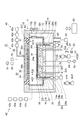
図1は、一実施形態に係るプラズマ処理方法を示す流れ図である。図1に示すプラズマ処理方法(以下、「方法MT」という)では、プラズマ処理装置を用いて基板に対してプラズマ処理が実行される。図2は、図1に示す方法の実行に用いることが可能な例示のプラズマ処理装置を示す図である。図2に示すプラズマ処理装置10は、容量結合型のプラズマ処理装置である。
FIG. 1 is a flow chart showing a plasma processing method according to an embodiment. In the plasma processing method shown in FIG. 1 (hereinafter, referred to as “method MT”), plasma processing is executed on the substrate using a plasma processing apparatus. FIG. 2 is a diagram illustrating an exemplary plasma processing apparatus that can be used to perform the method shown in FIG. The
プラズマ処理装置10は、チャンバ11を備えている。チャンバ11の中には内部空間Sが提供されている。内部空間Sは、第1空間S1及び第2空間S2を含んでいる。チャンバ11は、チャンバ本体12を含んでいる。チャンバ本体12は、略円筒形状を有している。チャンバ本体12の中には、内部空間Sが提供されている。チャンバ本体12は、例えばアルミニウムから構成されている。チャンバ本体12は接地電位に接続されている。チャンバ本体12の内壁面、即ち、内部空間Sを画成するチャンバ本体12の表面には、耐腐食性を有する膜が形成されている。この膜は、陽極酸化処理によって形成された膜、又は、酸化イットリウムから形成された膜といったセラミック製の膜であり得る。
The
チャンバ本体12の側壁には通路12pが形成されている。基板Wは、内部空間Sとチャンバ11の外部との間で搬送されるときに、通路12pを通過する。通路12pは、ゲートバルブ12gによって開閉可能である。ゲートバルブ12gは、チャンバ本体12の側壁に沿って設けられている。
A
内部空間Sの中には、隔壁14が設けられている。隔壁14は、第1空間S1と第2空間S2の境界上で延在している。隔壁14には、第1空間S1と第2空間S2とを互いに連通させるように、複数の貫通孔が形成されている。隔壁14は、母材の表面に耐腐食性を有する膜を形成することにより構成され得る。耐腐食性を有する膜は、極酸化処理によって形成された膜、又は、酸化イットリウムから形成された膜といったセラミック製の膜であり得る。母材は、例えばアルミニウムといった材料から形成される。隔壁14には、通路12pに対面するように開口が形成されている。基板Wは、第1空間S1とチャンバ11の外部との間で搬送されるときに、通路12p及び隔壁14の開口を通過する。隔壁14の開口は、シャッターSHによって開閉可能である。
A
隔壁14は、シールド部14a及びバッフルプレート14bを含み得る。シールド部14aは、略筒形状を有している。シールド部14aは、内部空間Sの中でチャンバ本体12の側壁に沿って鉛直方向に延在している。シールド部14aは、チャンバ本体12の側壁から離間している。シールド部14aの上端は、チャンバ11の上部まで延びており、当該上部に固定されている。プラズマ処理装置10では、第1空間S1内でプラズマエッチングといった基板処理が行われる。基板処理では反応生成物といった副生成物が発生する。シールド部14aにより、チャンバ本体12の表面に付着する副生成物の量が低減される。
The
バッフルプレート14bは、シールド部14aに交差する方向に延びている。バッフルプレート14bは、シールド部14aと後述する支持台との間で延在している。隔壁14の上述の複数の貫通孔は、バッフルプレート14bに形成されている。なお、シールド部14a及びバッフルプレート14bは一体に形成されていてもよく、互いから分離可能であってもよい。
The
内部空間Sの中では、支持部15が、チャンバ本体12の底部から上方に延在している。支持部15は、略円筒形状を有しており、石英といった絶縁材料から形成されている。支持部15上には支持台16が搭載されている。支持台16は、支持部15によって支持されている。支持台16は、第1空間S1の中で基板Wを支持するように構成されている。支持台16は、下部電極18及び静電チャック20を含んでいる。支持台16は、電極プレート21を更に含んでいてもよい。電極プレート21は、アルミニウムといった導電性材料から形成されており、略円盤形状を有している。下部電極18は、電極プレート21上に設けられている。下部電極18は、アルミニウムといった導電性材料から形成されており、略円盤形状を有している。下部電極18は、電極プレート21に電気的に接続されている。
In the internal space S, the
下部電極18内には、流路18fが設けられている。流路18fは、熱交換媒体用の流路である。熱交換媒体としては、例えば、液状の冷媒、又は、その気化によって下部電極18を冷却する冷媒(例えば、フロン)が用いられる。流路18fには、チラーユニットから配管22aを介して熱交換媒体が供給される。チラーユニットは、チャンバ本体12の外部に設けられている。流路18fに供給された熱交換媒体は、配管22bを介してチラーユニットに戻される。即ち、熱交換媒体は、流路18fとチラーユニットとの間で循環するように供給される。
A flow path 18f is provided in the lower electrode 18. The flow path 18f is a flow path for the heat exchange medium. As the heat exchange medium, for example, a liquid refrigerant or a refrigerant (for example, chlorofluorocarbon) that cools the lower electrode 18 by vaporization thereof is used. A heat exchange medium is supplied from the chiller unit to the flow path 18f via the
静電チャック20は、下部電極18上に設けられている。静電チャック20は、本体及び電極を有している。静電チャック20の本体は、誘電体から形成されており、略円盤形状を有している。静電チャック20の電極は、膜状の電極であり、静電チャック20の本体内に設けられている。静電チャック20の電極には、直流電源23がスイッチ24を介して電気的に接続されている。直流電源23から静電チャック20の電極に電圧が印加されると、静電チャック20上に載置された基板Wと静電チャック20との間で静電引力が発生する。発生した静電引力により、基板Wは、静電チャック20に引き付けられ、静電チャック20によって保持される。
The
プラズマ処理装置10には、ガス供給ライン25が設けられている。ガス供給ライン25は、ガス供給機構からの伝熱ガス、例えばHeガスを、静電チャック20の上面と基板Wの裏面(下面)との間に供給する。
The
静電チャック20の中には、一つ以上のヒータHT20(例えば抵抗発熱体)が設けられていてもよい。一つ以上のヒータHT20には、ヒータコントローラHC20から電力が与えられる。一つ以上のヒータHT20とヒータコントローラHC20との間には、ヒータコントローラHC20に高周波電力が流入することを防止するために、高周波フィルタFT20が設けられていてもよい。複数のヒータHT20が静電チャック20の中に設けられている場合には、ヒータコントローラHC20から複数のヒータHT20に与えられる電力を個別に調整することにより、静電チャック20の複数の領域のそれぞれの温度を個別に調整し、静電チャック20の面内(即ち、基板Wの面内)の温度分布を調整することが可能である。
One or more heaters HT20 (for example, a resistance heating element) may be provided in the
静電チャック20の外周領域上には、フォーカスリングFRが配置される。フォーカスリングFRは、略環状板形状を有している。フォーカスリングFRは、シリコン、石英、又は炭化シリコンといったシリコン含有材料から形成されている。フォーカスリングFRは、基板Wのエッジを囲むように配置される。フォーカスリングFRの中には、ヒータHTF(例えば抵抗発熱体)が設けられていてもよい。ヒータHTFは、ヒータコントローラHCFからヒータHTFに電力が与えられることにより、発熱する。ヒータHTFとヒータコントローラHCFとの間には、ヒータコントローラHCFに高周波電力が流入することを防止するために、高周波フィルタFTFが設けられていてもよい。
A focus ring FR is arranged on the outer peripheral region of the
チャンバ本体12の底部からは、筒状部26が上方に延在している。筒状部26は、支持部15の外周に沿って延在している。筒状部26は、導電性材料から形成されており、略円筒形状を有している。筒状部26は、接地電位に接続されている。筒状部26の表面は、耐腐食性を有する膜から形成されていてもよい。耐腐食性を有する膜は、極酸化処理によって形成された膜、又は、酸化イットリウムから形成された膜といったセラミック製の膜であり得る。
A
筒状部26上には、絶縁部28が設けられている。絶縁部28は、絶縁性を有し、石英といったセラミックから形成されている。絶縁部28は、略円筒形状を有しており、電極プレート21の外周、下部電極18の外周、及び静電チャック20の外周に沿って延在している。なお、上述したバッフルプレート14bの縁部は、筒状部26と絶縁部28との間に設けられ、筒状部26と絶縁部28によって挟持されていてもよい。
An insulating
プラズマ処理装置10は、駆動機構29を更に備えている。駆動機構29は、フォーカスリングFRを昇降させるように構成されている。駆動機構29は、一つ以上の駆動ユニット29uを含んでいる。図示された例では、駆動機構29は、二つの駆動ユニット29uを含んでいる。
The
駆動ユニット29uの各々は、ロッド29a、リフタ29b、及び駆動装置29cを含んでいる。ロッド29aは、柱状をなしており、鉛直方向に延在している。ロッド29aは、フォーカスリングFRを支持している。例えば、ロッド29aの先端が、フォーカスリングFRの下面に接続されている。ロッド29aは、内部空間Sの中では、例えば絶縁部28及び筒状部26を貫通する貫通孔を通って延在している。ヒータHTF用の給電ラインは、内部空間Sの中ではロッド29aの中で延在しており、チャンバ11の外側まで延びて高周波フィルタFTFを介してヒータコントローラHCFに接続している。
Each of the
駆動装置29cは、リフタ29bを介してロッド29aを昇降させる。駆動装置29cは、例えばステッピングモータである。駆動機構29は、電源システム29dを更に含む。電源システム29dは、パルス電流を駆動装置29cに供給するように構成されている。パルス電流が電源システム29dから駆動装置29cに供給されると、フォーカスリングFRは、ロッド29aを介して上昇又は下降する。
The
プラズマ処理装置10は、上部電極30を更に備えている。上部電極30は、支持台16の上方に設けられている。上部電極30は、部材32と共にチャンバ本体12の上部開口を閉じている。部材32は、絶縁性を有している。上部電極30は、この部材32を介してチャンバ本体12の上部に支持されている。
The
上部電極30は、天板34及び支持体36を含んでいる。天板34の下面は、内部空間S(又は第1空間S1)を画成している。天板34には、複数のガス吐出孔34aが設けられている。複数のガス吐出孔34aの各々は、天板34を板厚方向(鉛直方向)に貫通している。この天板34は、限定されるものではないが、例えばシリコンから形成されている。或いは、天板34は、母材の表面に耐腐食性を有する膜を設けた構造を有し得る。この膜は、陽極酸化処理によって形成された膜、又は、酸化イットリウムから形成された膜といったセラミック製の膜であり得る。母材は、例えばアルミニウムといった導電性材料から形成される。
The
支持体36は、天板34を着脱自在に支持する部品である。支持体36は、例えばアルミニウムといった導電性材料から形成され得る。支持体36の内部には、ガス拡散室36aが設けられている。ガス拡散室36aからは、複数のガス孔36bが下方に延びている。複数のガス孔36bは、複数のガス吐出孔34aにそれぞれ連通している。支持体36には、ガス導入口36cが形成されている。ガス導入口36cは、ガス拡散室36aに連通している。ガス導入口36cには、ガス供給管38が接続されている。
The
ガス供給管38には、ガス供給部40が接続されている。ガス供給部40は、後述するガス供給部42と共に、ガス供給系を構成している。ガス供給系は、第1空間S1に接続されている。ガス供給部40は、ガスソース群40s、バルブ群40a、流量制御器群40b、及びバルブ群40cを有している。
A
ガスソース群40sは、複数のガスソースを含んでいる。複数のガスソースは、方法MTで用いられる複数のガスのソースを含んでいる。複数のガスソースは、後述する有機膜を形成するための第1のガス及び第2のガスのうち一方のガスのソースを含んでいる。また、複数のガスソースは、基板Wのプラズマ処理に用いられる一つ以上のガスのソースを含んでいる。また、複数のガスソースは、後述するパージにおいて用いられる不活性ガスのソースを含み得る。
The
バルブ群40a及びバルブ群40cの各々は、複数のバルブを含んでいる。流量制御器群40bは、複数の流量制御器を含んでいる。流量制御器群40bの複数の流量制御器の各々は、マスフローコントローラ又は圧力制御式の流量制御器である。ガスソース群40sの複数のガスソースの各々は、バルブ群40aの対応のバルブ、流量制御器群40bの対応の流量制御器、及びバルブ群40cの対応のバルブを介して、ガス供給管38に接続されている。ガス供給部40からのガスは、ガス供給管38、ガス拡散室36a、複数のガス孔36b、及び複数のガス吐出孔34aを介して、第1空間S1に供給される。
Each of the
プラズマ処理装置10は、ガス供給部42を更に備えている。ガス供給部42は、ガスソース42s、バルブ42a、流量制御器42b、及びバルブ42cを有している。ガスソース42sは、第1のガス及び第2のガスのうち他方のガスのソースである。流量制御器42bは、マスフローコントローラ又は圧力制御式の流量制御器である。ガスソース42sは、バルブ42a、流量制御器42b、及びバルブ42cを介して、第1空間S1に接続されている。ガス供給部42からのガスは、第1空間S1に供給される。
The
プラズマ処理装置10のチャンバ本体12の底部には、排気管50が接続されている。排気管50には、排気装置52が接続されている。排気装置52は、排気管50を介して、第2空間S2に接続されている。また、排気装置52は、第2空間S2及び隔壁14の複数の貫通孔を介して第1空間S1に接続されている。排気装置52は、圧力調整弁及び減圧ポンプを含んでいる。減圧ポンプは、圧力調整弁を介して第2空間S2に接続されている。減圧ポンプは、ターボ分子ポンプ及び/又はドライポンプであり得る。
An
プラズマ処理装置10は、第1空間S1に供給されるガスのプラズマを第1空間S1内で生成することが可能である。プラズマ処理装置10は、第1の高周波電源61を更に備えている。第1の高周波電源61は、プラズマ生成用の第1の高周波電力を発生する電源である。第1の高周波電力は、例えば、27〜100MHzの範囲内の周波数を有する。第1の高周波電源61は、整合器63を介して上部電極30に接続されている。整合器63は、第1の高周波電源61の出力インピーダンスと負荷側(上部電極30側)のインピーダンスを整合させるためのマッチング回路を有している。なお、第1の高周波電源61は、整合器63を介して下部電極18に接続されていてもよい。この場合には、上部電極30は電気的に接地される。
The
プラズマ処理装置10は、第2の高周波電源62を更に備え得る。第2の高周波電源62は、基板Wにイオンを引き込むためのバイアス用の第2の高周波電力を発生する電源である。第2の高周波電力の周波数は、第1の高周波電力の周波数よりも低い。第2の高周波電力の周波数は、例えば、400kHz〜13.56MHzの範囲内の周波数である。第2の高周波電源62は、整合器64を介して下部電極18に接続されている。整合器64は、第2の高周波電源62の出力インピーダンスと負荷側(下部電極18側)のインピーダンスを整合させるためのマッチング回路を有している。
The
プラズマ処理装置10では、第1空間S1にガスが供給されている状態で第1の高周波電力が供給されると、当該ガスが励起される。その結果、第1空間S1内でプラズマが生成される。第2の高周波電力が下部電極18に供給されると、プラズマ中のイオンが基板Wに向けて加速される。
In the
プラズマ処理装置10は、直流電源70を更に備えている。直流電源70は、上部電極30に接続されている。直流電源70は負極性の直流電圧を上部電極30に印加するように構成されている。上部電極30に負極性の直流電圧が印加されると、第1空間S1内で生成されたプラズマ中の正イオンが上部電極30の天板34に衝突する。正イオンが天板34に衝突すると、天板34から二次電子が放出される。天板34がシリコンから形成されている場合には、正イオンが天板34に衝突すると、天板34からシリコンが放出され得る。
The
一実施形態では、プラズマ処理装置10は、制御部80を更に備え得る。制御部80は、プラズマ処理装置10の各部を制御するよう構成されている。制御部80は、プロセッサ、メモリといった記憶装置、入力装置、表示装置等を備えるコンピュータであり得る。制御部80は、記憶装置に記憶されている制御プログラムを実行し、当該記憶装置に記憶されているレシピデータに基づいてプラズマ処理装置10の各部を制御する。これにより、プラズマ処理装置10は、レシピデータによって指定されたプロセスを実行する。例えば、制御部80は、方法MTの実行においてプラズマ処理装置10の各部を制御し、且つ、後述する種々の演算及び判定といった処理を実行する。制御部80の記憶装置には、方法MTの実行において利用される各種データが登録されている。
In one embodiment, the
以下、再び図1を参照して、方法MTについて詳細に説明する。以下の説明では、プラズマ処理装置10が用いられる場合を例として、方法MTについて記述する。また、以下の説明では、図3〜図7を参照する。図3〜図7の各々は、フォーカスリングの状態とイオンの入射方向との例示的関係を示す図である。図3〜図7において、円形の図形は、イオンを表している。
Hereinafter, the method MT will be described in detail with reference to FIG. 1 again. In the following description, the method MT will be described by taking the case where the
方法MTでは、支持台16(静電チャック20)上に基板Wが載置される。そして、最初の工程STP(1)において基板Wに対してプラズマ処理P(1)が実行される。「P(i)」は、方法MTにおいてi回目に実行される工程STP(i)のプラズマ処理を表している。「i」は、1以上の整数である。 In the method MT, the substrate W is placed on the support base 16 (electrostatic chuck 20). Then, in the first step STP (1), the plasma processing P (1) is executed on the substrate W. “P (i)” represents the plasma treatment of step STP (i) executed in the i-th time in the method MT. "I" is an integer of 1 or more.
プラズマ処理P(i)の条件は、制御部80の記憶装置に記憶されているレシピデータにおいて指定されている。工程STP(i)の実行時には、シャッターSHが隔壁14の開口を閉じている。工程STP(i)では、プラズマ処理P(i)用の処理ガスが内部空間S(第1空間S1)に供給される。工程STP(i)では、プラズマ処理P(i)のために指定された圧力に内部空間Sの中の圧力を設定するよう、排気装置52が制御される。工程STP(i)では、第1の高周波電力が供給される。第1の高周波電力の電力レベルは、プラズマ処理P(i)のために指定された電力レベルに設定される。工程STP(i)では、第2の高周波電力が更に供給されてもよい。第2の高周波電力の電力レベルは、プラズマ処理P(i)のために指定された電力レベルに設定される。その結果、工程STP(i)では、処理ガスのプラズマが生成される。基板Wは、プラズマからのイオンによって処理される。例えば、基板Wは、プラズマからのイオンによってエッチングされる。
The conditions of the plasma processing P (i) are specified in the recipe data stored in the storage device of the
図3に示すように、新しいフォーカスリングFRが用いられて最初のプラズマ処理P(i)、即ちプラズマ処理P(1)が実行されるときには、鉛直方向におけるフォーカスリングFRの上面の位置は、基準位置RPに一致する。鉛直方向におけるフォーカスリングFRの上面の位置が基準位置RPに略一致している場合には、シースとプラズマとの界面BSの形状は、プラズマからのイオンが基板Wの上面の全体に垂直に入射するような形状となる。例えば、シースとプラズマとの界面BSの形状は、基板の中央の上方の位置からフォーカスリングFRの上方の位置にわたって略平坦な形状となる。プラズマ処理がプラズマエッチングである場合には、プラズマからのイオンが基板Wの上面の全体に垂直に入射すると、垂直に延びる複数の開口が基板Wの全体で形成される。なお、基準位置RPは、例えば、支持台16上に載置された基板Wの上面の鉛直方向における位置であり得る。なお、基準位置RPは、基板Wの全体にわたって、イオンが垂直に入射するように定められた位置であれば、如何なる位置であってもよい。
As shown in FIG. 3, when the first plasma processing P (i), that is, the plasma processing P (1) is executed by using the new focus ring FR, the position of the upper surface of the focus ring FR in the vertical direction is a reference. Matches position RP. When the position of the upper surface of the focus ring FR in the vertical direction substantially coincides with the reference position RP, the shape of the interface BS between the sheath and the plasma is such that ions from the plasma are vertically incident on the entire upper surface of the substrate W. It will be shaped like a plumb bob. For example, the shape of the interface BS between the sheath and the plasma is substantially flat from the position above the center of the substrate to the position above the focus ring FR. When the plasma treatment is plasma etching, when ions from the plasma are vertically incident on the entire upper surface of the substrate W, a plurality of vertically extending openings are formed in the entire substrate W. The reference position RP may be, for example, a position in the vertical direction of the upper surface of the substrate W placed on the
工程STP(i)のプラズマ処理P(i)により、フォーカスリングFRはエッチングされる。即ち、工程STP(i)のプラズマ処理P(i)により、フォーカスリングFRが消耗して、フォーカスリングFRの厚みが減少する。フォーカスリングFRの厚みが減少すると、鉛直方向におけるフォーカスリングFRの上面の位置と基準位置RPとの間に差が生じる。鉛直方向におけるフォーカスリングFRの上面の位置と基準位置RPとの間に差が生じると、図4に示すように、基板Wのエッジの上方の領域において、界面BSの形状が変形する。その結果、プラズマからのイオンは、基板Wのエッジに斜めに入射する。プラズマ処理がプラズマエッチングである場合には、プラズマからのイオンが基板Wのエッジに斜めに入射すると、基板Wのエッジにおいて開口が斜めに形成される。 The focus ring FR is etched by the plasma treatment P (i) in the step STP (i). That is, the plasma treatment P (i) in the step STP (i) consumes the focus ring FR and reduces the thickness of the focus ring FR. When the thickness of the focus ring FR decreases, a difference occurs between the position of the upper surface of the focus ring FR in the vertical direction and the reference position RP. When a difference occurs between the position of the upper surface of the focus ring FR in the vertical direction and the reference position RP, the shape of the interface BS is deformed in the region above the edge of the substrate W as shown in FIG. As a result, the ions from the plasma are obliquely incident on the edge of the substrate W. When the plasma treatment is plasma etching, when ions from the plasma are obliquely incident on the edge of the substrate W, an opening is formed obliquely at the edge of the substrate W.
方法MTでは、基準位置RPと鉛直方向におけるフォーカスリングFRの上面の位置との差を減少させるために、工程ST13が実行され得る。工程ST13では、フォーカスリングFR上に有機膜OFが選択的に形成される。かかる工程ST13の実行後に、工程STP(i)においてプラズマ処理P(i)が実行される。 In the method MT, step ST13 may be performed to reduce the difference between the reference position RP and the position of the top surface of the focus ring FR in the vertical direction. In step ST13, the organic film OF is selectively formed on the focus ring FR. After the execution of the step ST13, the plasma treatment P (i) is executed in the step STP (i).
再び図1を参照する。方法MTでは、2回目以降の工程STP(i)のプラズマ処理P(i)の実行前に、工程ST1が実行される。工程ST1では、プラズマ処理P(i−1)の実行後のフォーカスリングFR上の有機膜OFの残膜の膜厚FOF_Lが、(1)式により制御部80によって算出される。
FOF_L=FOF_CUR−TP(i−1)×EP_OF(P(i−1)) …(1)
なお、プラズマ処理P(i−1)は、(i−1)回目に実行された工程STP(i−1)のプラズマ処理である。
See FIG. 1 again. In the method MT, the step ST1 is executed before the execution of the plasma treatment P (i) of the second and subsequent steps STP (i). In step ST1, the film thickness FOF_L of the residual film of the organic film OF on the focus ring FR after the execution of the plasma treatment P (i-1) is calculated by the
F OF_L = F OF_CUR -T P ( i-1) × E P_OF (P (i-1)) ... (1)
The plasma treatment P (i-1) is the plasma treatment of the step STP (i-1) executed in the (i-1) th time.
(1)式において、FOF_CURは、プラズマ処理P(i−1)の直前に形成された有機膜OFの膜厚である。TP(j)は、j回目に実行される工程STP(j)のプラズマ処理P(j)の実行時間長である。したがって、(1)式におけるTP(i−1)は、プラズマ処理P(i−1)の実行時間長である。EP_OF(P(j))は、プラズマ処理P(j)による有機膜OFのエッチングレートである。したがって、(1)式におけるEP_OF(P(i−1))は、プラズマ処理P(i−1)による有機膜OFのエッチングレートである。実行時間長TP(j)及びエッチングレートEP_OF(P(j))は、制御部80の記憶装置に登録されている。なお、膜厚FOF_Lの下限値は0である。例えば、プラズマ処理P(2)の直前に実行される工程ST1では、その前に有機膜OFが形成されていないので、膜厚FOF_Lは0である。
In the equation (1), F OF_CUR is the film thickness of the organic film OF formed immediately before the plasma treatment P (i-1). T P (j) is the execution time length of the plasma processing P (j) of the step STP (j) executed at the jth time. Therefore, TOP (i-1) in the equation (1) is the execution time length of the plasma processing P (i-1). E P_OF (P (j)) is the etching rate of the organic film OF by the plasma treatment P (j). Therefore, EP_OF (P (i-1)) in the equation (1) is the etching rate of the organic film OF by the plasma treatment P (i-1). The execution time length T P (j) and the etching rate EP_OF (P (j)) are registered in the storage device of the
続く工程ST2では、有機膜OFの残膜が存在するか否かが判定される。即ち、工程ST2では、膜厚FOF_Lが0より大きいか否かが判定される。膜厚FOF_Lが0である場合には、工程ST4に遷移する。一方、膜厚FOF_Lが0より大きい場合には、工程ST3が実行される。 In the subsequent step ST2, it is determined whether or not there is a residual film of the organic film OF. That is, in step ST2, it is determined whether or not the film thickness FOF_L is larger than 0. When the film thickness F OF_L is 0, the process proceeds to step ST4. On the other hand, when the film thickness F OF_L is larger than 0, the step ST3 is executed.
工程ST3では、有機膜OFの残膜が除去される。工程ST3の実行時には、シャッターSHが隔壁14の開口を閉じている。一実施形態において、有機膜OFは、プラズマエッチングによって除去される。プラズマエッチングのために、第1空間S1の中で除去ガスのプラズマが生成される。除去ガスは、酸素含有ガスを含み得る。酸素含有ガスは、酸素ガス(O2ガス)、COガス、又はCO2ガスであり得る。或いは、除去ガスは、水素ガス(H2ガス)及び窒素ガス(N2ガス)の混合ガスを含み得る。別の実施形態では、有機膜OFが解重合し得る場合に、有機膜OFを解重合させるように、フォーカスリングFRがヒータHTFによって加熱されてもよい。解重合によって生成された有機化合物の気体は、排気される。工程ST3において有機膜OFの残膜が除去された後には、工程ST4が実行される。
In step ST3, the residual film of the organic film OF is removed. When the step ST3 is executed, the shutter SH closes the opening of the
工程ST3におけるプラズマエッチングの実行時間長は、TREMであり、以下の(2)式により算出される。
TREM=FOF_L/EREM_OF×M …(2)
(2)式において、EREM_OFは、工程ST3のプラズマエッチングにおける有機膜OFのエッチングレートであり、制御部80の記憶装置に登録されている。(2)式において、Mは、制御部80の記憶装置に登録されている数値であり、1より大きい。したがって、実行時間長TREMは、以下の(3)式で定義されるオーバーエッチングの時間長TOEを含む。
TOE=FOF_L/EREM_OF×(M−1) …(3)
The execution time length of plasma etching in step ST3 is TREM , and is calculated by the following equation (2).
T REM = F OF_L / E REM_OF x M ... (2)
In the equation (2), EREM_OF is the etching rate of the organic film OF in the plasma etching in step ST3, and is registered in the storage device of the
T OE = F OF_L / E REM_OF × (M-1)… (3)
工程ST4では、フォーカスリングFRの厚みの減少量DCURが制御部80によって算出される。減少量DCURは、以下の(4)式により算出される。
DCUR=TFR_ETCH×EP_FR(P(i−1))+TOE×EOE_FR …(4)
In step ST4, the reduction amount D CUR of the thickness of the focus ring FR is calculated by the
D CUR = T FR_ETCH x E P_FR (P (i-1)) + T OE x E OE_FR ... (4)
EP_FR(P(j))は、プラズマ処理P(j)によるフォーカスリングのエッチングレートであり、制御部80の記憶装置に登録されている。(4)式におけるEP_FR(P(i−1))は、プラズマ処理P(i−1)によるフォーカスリングのエッチングレートである。(4)式において、EOE_FRは、工程ST3のオーバーエッチングによるフォーカスリングFRのエッチングレートであり、制御部80の記憶装置に登録されている。(4)式において、TFR_ETCHは、プラズマ処理P(i−1)において、フォーカスリングFR上の有機膜OFが消失した時点からのプラズマ処理P(i−1)の終了時点までの時間長である。時間長TFR_ETCHは、以下の式(5)により求められる。
TFR_ETCH=TP(i−1)−FOF_CUR/EP_OF(P(i−1)) …(5)
EP_FR (P (j)) is the etching rate of the focus ring by the plasma processing P (j), and is registered in the storage device of the
T FR_ETCH = T P (i-1) -F OF_CUR / E P_OF (P (i-1)) ... (5)
工程ST4に続く工程ST5では、減少量DCURの積算量DACMが、制御部80によって算出される。積算量DACMは、以下の式(6)により算出される。
DACM=DACM+DCUR …(6)
In subsequent step ST4 step ST5, the integrated amount D ACM decrease amount D CUR is calculated by the
D ACM = D ACM + D CUR ... (6)
続く工程ST6では、目標補正量CTが制御部80によって算出される。目標補正量CTは、鉛直方向におけるフォーカスリングFRの上面の位置と基準位置RPとの間の差を反映する量である。目標補正量CTは、以下の(7)式により算出される。
CT=DACM−UACM …(7)
(7)式において、UACMは、フォーカスリングFRが初期の位置に対して既に上昇している量(距離)の積算量である。
In the subsequent step ST6, the target correction amount C T is calculated by the
C T = D ACM -U ACM ... (7)
In the equation (7), the UACM is an integrated amount of the amount (distance) that the focus ring FR has already risen with respect to the initial position.
続く工程ST7では、フォーカスリングFRの厚みの減少量の積算量DACMが基準値RTHよりも大きいか否かが判定される。基準値RTHは、制御部80の記憶装置に登録されている。積算量DACMが基準値RTHよりも大きい場合には、工程ST8において、フォーカスリングFRが新しいフォーカスリングFRに交換され、工程STP(i)に遷移する。一方、積算量DACMが基準値RTH以下である場合には、工程ST9に遷移する。
In the subsequent step ST7, whether integrated amount D ACM of reduction of the thickness of the focus ring FR is larger than the reference value R TH is determined. The reference value R TH is registered in the storage device of the
工程ST9では、目標補正量CTが、最小移動制御量UMIN以上であるか否かが判定される。最小移動制御量UMINは、制御部80の記憶装置に登録されている。駆動機構29は、最小移動制御量UMINを最小距離としてフォーカスリングFRを上昇させることができる。即ち、駆動機構29は、最小移動制御量UMINの整数倍の距離で、フォーカスリングFRを上昇させることができる。目標補正量CTが最小移動制御量UMINよりも小さい場合には、工程ST11に遷移する。目標補正量CTが最小移動制御量UMIN以上である場合には、工程ST10において、フォーカスリングFRを上昇させるよう、駆動機構29が制御される。駆動機構29は、目標補正量CT以下の最大の移動量UCURで、フォーカスリングFRを上昇させる。そして、移動量UCURを用いて積算量UACMが更新される。具体的には、以下の式(8)の演算が制御部80によって行われる。
UACM=UACM+UCUR …(8)
しかる後に、工程ST11が実行される。
In step ST9, the target correction amount C T is, whether or not the minimum movement control amount U MIN or not is determined. The minimum movement control amount UMIN is registered in the storage device of the
U ACM = U ACM + U CUR ... (8)
After that, step ST11 is executed.
工程ST11では、目標成膜量FTが制御部80によって算出される。目標成膜量FTは、以下の式(9)により算出される。
FT=CT−UCUR …(9)
In step ST11, the target deposition amount F T is calculated by the
F T = C T -U CUR ... (9)
続く工程ST12では、目標成膜量FTが最小成膜制御量FMIN以上であるか否かが判定される。最小成膜制御量FMINは、制御部80の記憶装置に登録されている。最小成膜制御量FMINは、最小移動制御量UMINよりも小さい量であり得る。後述する工程ST13では、最小成膜制御量FMINを最小の厚みとして有機膜OFを形成することができる。即ち、工程ST13では、最小成膜制御量FMINの整数倍の厚みで、有機膜OFを形成することができる。目標成膜量FTが最小成膜制御量FMINよりも小さい場合には、工程STP(i)に遷移する。一方、目標成膜量FTが最小成膜制御量FMIN以上である場合には、工程ST13が実行される。
In the subsequent step ST12, whether the target film formation amount F T is minimum film forming control amount F MIN or not is determined. The minimum film formation control amount F MIN is registered in the storage device of the
工程ST13では、目標補正量CTから移動量UCURを差し引いた量を減少させるように、フォーカスリングFR上に有機膜OFが形成される。工程ST13において、有機膜OFは、(CT−UCUR)以下、即ち、目標成膜量FT以下、且つ、最小成膜制御量FMIN以上の最大の厚みで、形成される。 In step ST13, so as to reduce the amount obtained by subtracting the amount of movement U CUR from the target correction amount C T, the organic film OF is formed on the focus ring FR. In step ST13, the organic film OF is, (C T -U CUR) below, i.e., below the target deposition amount F T, and a minimum film forming control amount F MIN or more of the maximum thickness is formed.
一実施形態における工程ST13では、有機膜OFを形成するために、第1のガス及び第2のガスが、交互に又は同時に第1空間S1に供給される。第1のガス及び第2のガスは、第1空間S1を介して第2空間S2にも供給される。第1のガス及び第2のガスのうち一方は、ガス供給部40によって供給される。第1のガス及び第2のガスのうち他方は、ガス供給部42によって供給される。工程ST13では、内部空間Sの中の圧力が指定された圧力に設定されるよう、排気装置52が制御される。工程ST13では、内部空間Sの中でプラズマは生成されない。
In step ST13 in one embodiment, the first gas and the second gas are alternately or simultaneously supplied to the first space S1 in order to form the organic film OF. The first gas and the second gas are also supplied to the second space S2 via the first space S1. One of the first gas and the second gas is supplied by the
工程ST13において第1のガス及び第2のガスが交互に第1空間S1に供給される場合には、第1のガスの供給後、第2のガスの供給前に、内部空間Sのパージが実行されてもよい。また、工程ST13において第1のガス及び第2のガスが交互に第1空間S1に供給される場合には、第2のガスの供給後、第1のガスの供給前に、内部空間Sのパージが実行されてもよい。内部空間Sのパージでは、内部空間Sの中のガスが排気装置52によって排気される。加えて、内部空間Sのパージでは、不活性ガスがガス供給部40から内部空間に供給されてもよい。不活性ガスは、例えば希ガス又は窒素ガスである。
When the first gas and the second gas are alternately supplied to the first space S1 in the step ST13, the internal space S is purged after the supply of the first gas and before the supply of the second gas. It may be executed. Further, when the first gas and the second gas are alternately supplied to the first space S1 in the step ST13, the internal space S is supplied after the supply of the second gas and before the supply of the first gas. A purge may be performed. In the purging of the internal space S, the gas in the internal space S is exhausted by the
第1のガスは、第1の有機化合物を含む。第2のガスは、第2の有機化合物を含む。有機膜OFは、第1の有機化合物と第2の有機化合物との重合により形成される。第1の有機化合物と第2の有機化合物との重合は、第1の温度範囲内の温度の環境下で生じる。第1の温度範囲は、例えば0℃以上、150℃以下の温度範囲である。即ち、第1の有機化合物と第2の有機化合物との重合は、第1の温度範囲の下限温度よりも低い第2の温度範囲の温度では生じない。また、第1の有機化合物と第2の有機化合物との重合は、第1の温度範囲の上限温度よりも高い第3の温度範囲では生じない。第3の温度範囲は、例えば250℃以上、400℃以下の温度である。なお、第1の有機化合物と第2の有機化合物との重合により形成される有機化合物は、第3の温度範囲内の温度の環境下では第1の有機化合物と第2の有機化合物に解重合してもよい。 The first gas contains the first organic compound. The second gas contains a second organic compound. The organic film OF is formed by the polymerization of the first organic compound and the second organic compound. The polymerization of the first organic compound and the second organic compound occurs in an environment of a temperature within the first temperature range. The first temperature range is, for example, a temperature range of 0 ° C. or higher and 150 ° C. or lower. That is, the polymerization of the first organic compound and the second organic compound does not occur at a temperature in the second temperature range lower than the lower limit temperature in the first temperature range. Further, the polymerization of the first organic compound and the second organic compound does not occur in the third temperature range higher than the upper limit temperature of the first temperature range. The third temperature range is, for example, a temperature of 250 ° C. or higher and 400 ° C. or lower. The organic compound formed by the polymerization of the first organic compound and the second organic compound is depolymerized into the first organic compound and the second organic compound in an environment of a temperature within the third temperature range. You may.
一実施形態における工程ST13では、ヒータFTHによってフォーカスリングFRが第1の温度範囲の温度に加熱される。フォーカスリングFRとその周囲の部品(例えば支持台16)との接触面積は小さい。したがって、フォーカスリングFRは、その周囲の部品から熱的に分離されている。したがって、フォーカスリングFRが選択的に加熱され、フォーカスリングFR上で選択的に重合が生じる。その結果、フォーカスリングFR上で選択的に有機膜OFが形成される。 In step ST13 of one embodiment, the heater FTH heats the focus ring FR to a temperature in the first temperature range. The contact area between the focus ring FR and the surrounding components (for example, the support 16) is small. Therefore, the focus ring FR is thermally separated from its surrounding components. Therefore, the focus ring FR is selectively heated, and polymerization is selectively generated on the focus ring FR. As a result, the organic film OF is selectively formed on the focus ring FR.
以下、第1の有機化合物及び第2の有機化合物、並びに、第1の有機化合物と第2の有機化合物との重合により生成される有機化合物、即ち有機膜OFを構成する有機化合物について例示する。 Hereinafter, the first organic compound and the second organic compound, and the organic compound produced by the polymerization of the first organic compound and the second organic compound, that is, the organic compound constituting the organic film OF will be exemplified.
第1の有機化合物は、以下の式(1)又は式(2)に示すイソシアネートであることができ、第2の有機化合物は、以下の式(3)又は式(4)に示すアミンであることができる。即ち、第1の有機化合物は、一官能性イソシアネート又は二官能性イソシアネートであることができ、第2の有機化合物は、一官能性アミン又は二官能性アミンであることができる。
![]()
![]()
![]()
![]()
![]()
![]()
![]()
![]()
式(1)及び式(2)において、Rは、アルキル基(直鎖状アルキル基若しくは環状アルキル基)等の飽和炭化水素基、アリール基等の不飽和炭化水素基、又はN、O、S、F、若しくはSi等のヘテロ原子を含む基である。ヘテロ原子を含む基は、その一部の元素がN、O、S、F、若しくはSi等で置換された飽和炭化水素基又は不飽和炭化水素基を含む。第1の有機化合物であるイソシアネートとしては、例えば脂肪族化合物又は芳香族化合物を用いることができる。脂肪族化合物としては、脂肪族鎖式化合物又は脂肪族環式化合物を用いることができる。脂肪族化合物としては、例えばヘキサメチレンジイソシアネートが挙げられる。また、脂肪族環式化合物としては、例えば1,3−ビス(イソシアネートメチル)シクロヘキサン(H6XDI)が挙げられる。 In formulas (1) and (2), R is a saturated hydrocarbon group such as an alkyl group (linear alkyl group or cyclic alkyl group), an unsaturated hydrocarbon group such as an aryl group, or N, O, S. , F, or a group containing a hetero atom such as Si. A group containing a heteroatom includes a saturated hydrocarbon group or an unsaturated hydrocarbon group in which some of its elements are substituted with N, O, S, F, Si or the like. As the isocyanate which is the first organic compound, for example, an aliphatic compound or an aromatic compound can be used. As the aliphatic compound, an aliphatic chain compound or an aliphatic cyclic compound can be used. Examples of the aliphatic compound include hexamethylene diisocyanate. Examples of the aliphatic cyclic compound include 1,3-bis (isocyanatemethyl) cyclohexane (H6XDI).
式(3)及び式(4)において、Rは、アルキル基(直鎖状アルキル基若しくは環状アルキル基)等の飽和炭化水素基、アリール基等の不飽和炭化水素基、又はN、O、S、F、若しくはSi等のヘテロ原子を含む基である。ヘテロ原子を含む基は、その一部の元素がN、O、S、F、若しくはSi等で置換された飽和炭化水素基又は不飽和炭化水素基を含む。なお、式(1)及び式(2)においてRで示される原子団は、式(3)及び式(4)においてRで示される原子団と同一であってもよく、異なっていてもよい。第2の有機化合物であるアミンとしては、例えば脂肪族化合物又は芳香族化合物を用いることができる。脂肪族化合物としては、脂肪族鎖式化合物又は脂肪族環式化合物を用いることができる。脂肪族化合物としては、例えば1,12−ジアミノドデカン(DAD)が挙げられる。脂肪族環式化合物としては、1,3−ビス(アミノメチル)シクロヘキサン(H6XDA)が挙げられる。なお、第2の有機化合物であるアミンは、二級アミンであってもよい。 In formulas (3) and (4), R is a saturated hydrocarbon group such as an alkyl group (linear alkyl group or cyclic alkyl group), an unsaturated hydrocarbon group such as an aryl group, or N, O, S. , F, or a group containing a hetero atom such as Si. A group containing a heteroatom includes a saturated hydrocarbon group or an unsaturated hydrocarbon group in which some of its elements are substituted with N, O, S, F, Si or the like. The atomic group represented by R in the formulas (1) and (2) may be the same as or different from the atomic group represented by R in the formulas (3) and (4). As the amine which is the second organic compound, for example, an aliphatic compound or an aromatic compound can be used. As the aliphatic compound, an aliphatic chain compound or an aliphatic cyclic compound can be used. Aliphatic compounds include, for example, 1,12-diaminododecane (DAD). Examples of the aliphatic cyclic compound include 1,3-bis (aminomethyl) cyclohexane (H6XDA). The amine which is the second organic compound may be a secondary amine.
イソシアネートとアミンとの重合(付加縮合)によって得られる有機化合物としては、以下の式(5)〜式(8)に示す尿素結合を有する化合物が挙げられる。式(5)に示す化合物は、式(1)に示す化合物と式(3)に示す化合物との重合により、生成される。式(6)に示す化合物は、式(1)に示す化合物と式(4)に示す化合物との重合により、生成される。或いは、式(6)に示す化合物は、式(2)に示す化合物と式(3)に示す化合物との重合により、生成される。式(7)に示す化合物は、式(2)に示す化合物と式(4)に示す化合物との重合により、生成される。また、式(8)に示す化合物は、式(7)に示すポリマーの両末端をそれぞれ、イソシアネート基を有するモノマー(例えば式(1)に示す化合物)、アミノ基を有するモノマー(例えば式(3)に示す化合物)で終端させた構造を有する。なお、式(7)及び式(8)において、nは2以上の整数である。

別の例では、第1の有機化合物は、式(1)又は式(2)に示すイソシアネートであることができ、第2の有機化合物は、以下の式(9)又は式(10)に示す水酸基を有する化合物であることができる。即ち、第1の有機化合物は、一官能性イソシアネート又は二官能性イソシアネートであることができ、第2の有機化合物は、水酸基を有する一官能性化合物又は水酸基を有する二官能性化合物であることができる。
![]()
![]()
![]()
![]()
式(9)及び式(10)において、Rは、アルキル基(直鎖状アルキル基若しくは環状アルキル基)等の飽和炭化水素基、アリール基等の不飽和炭化水素基、又はN、O、S、F、若しくはSi等のヘテロ原子を含む基である。ヘテロ原子を含む基は、その一部の元素がN、O、S、F、若しくはSi等で置換された飽和炭化水素基又は不飽和炭化水素基を含む。なお、式(1)及び式(2)においてRで示される原子団は、式(9)及び式(10)においてRで示される原子団と同一であってもよく、異なっていてもよい。水酸基を有する化合物は、アルコール又はフェノールである。第2の有機化合物であるアルコールとしては、例えばエチレングリコールが挙げられる。また、第2の有機化合物であるフェノールとしては、例えばヒドロキノンが挙げられる。 In formulas (9) and (10), R is a saturated hydrocarbon group such as an alkyl group (linear alkyl group or cyclic alkyl group), an unsaturated hydrocarbon group such as an aryl group, or N, O, S. , F, or a group containing a hetero atom such as Si. A group containing a heteroatom includes a saturated hydrocarbon group or an unsaturated hydrocarbon group in which some of its elements are substituted with N, O, S, F, Si or the like. The atomic group represented by R in the formulas (1) and (2) may be the same as or different from the atomic group represented by R in the formulas (9) and (10). The compound having a hydroxyl group is an alcohol or phenol. Examples of the alcohol, which is the second organic compound, include ethylene glycol. Further, as the phenol which is the second organic compound, for example, hydroquinone can be mentioned.
イソシアネートと水酸基を有する化合物との重合(重付加)によって得られる有機化合物としては、以下の式(11)〜式(15)に示すウレタン結合を有する化合物が挙げられる。式(11)に示す化合物は、式(1)に示す化合物と式(9)に示す化合物との重合により、生成される。式(12)に示す化合物は、式(1)に示す化合物と式(10)に示す化合物との重合により、生成される。式(13)に示す化合物は、式(2)に示す化合物と式(9)に示す化合物との重合により、生成される。式(14)に示す化合物は、式(2)に示す化合物と式(10)に示す化合物との重合により、生成される。また、式(15)に示す化合物は、式(14)に示すポリマーの両末端をそれぞれ、イソシアネート基を有するモノマー(例えば式(1)に示す化合物)、水酸基を有するモノマー(例えば式(9)に示す化合物)で終端させた構造を有する。なお、式(14)及び式(15)において、nは2以上の整数である。
更に別の例では、第1の有機化合物は、以下の式(16)又は式(17)に示すカルボン酸であることができ、第2の有機化合物は、式(3)又は式(4)に示すアミンであることができる。即ち、第1の有機化合物は、一官能性カルボン酸又は二官能性カルボン酸であることができ、第2の有機化合物は、一官能性アミン又は二官能性アミンであることができる。
![]()
![]()
![]()
![]()
式(16)及び式(17)において、Rは、アルキル基(直鎖状アルキル基若しくは環状アルキル基)等の飽和炭化水素基、アリール基等の不飽和炭化水素基、又はN、O、S、F、若しくはSi等のヘテロ原子を含む基である。ヘテロ原子を含む基は、その一部の元素がN、O、S、F、若しくはSi等で置換された飽和炭化水素基又は不飽和炭化水素基を含む。なお、式(3)及び式(4)においてRで示される原子団は、式(16)及び式(17)においてRで示される原子団と同一であってもよく、異なっていてもよい。第1の有機化合物であるカルボン酸としては、例えばテレフタル酸が挙げられる。 In formulas (16) and (17), R is a saturated hydrocarbon group such as an alkyl group (linear alkyl group or cyclic alkyl group), an unsaturated hydrocarbon group such as an aryl group, or N, O, S. , F, or a group containing a hetero atom such as Si. A group containing a heteroatom includes a saturated hydrocarbon group or an unsaturated hydrocarbon group in which some of its elements are substituted with N, O, S, F, Si or the like. The atomic group represented by R in the formulas (3) and (4) may be the same as or different from the atomic group represented by R in the formulas (16) and (17). Examples of the carboxylic acid which is the first organic compound include terephthalic acid.
カルボン酸とアミンとの重合(重縮合)によって得られる有機化合物としては、以下の式(18)〜式(22)に示すアミド結合を有する化合物、例えばポリアミドが挙げられる。式(18)に示す化合物は、式(16)に示す化合物と式(3)に示す化合物との重合により、生成される。式(19)に示す化合物は、式(16)に示す化合物と式(4)に示す化合物との重合により、生成される。式(20)に示す化合物は、式(17)に示す化合物と式(3)に示す化合物との重合により、生成される。式(21)に示す化合物は、式(17)に示す化合物と式(4)に示す化合物との重合により、生成される。また、式(22)に示す化合物は、式(21)に示すポリマーの両末端をそれぞれ、カルボキシル基を有するモノマー(例えば式(16)に示す化合物)、アミノ基を有するモノマー(例えば式(3)に示す化合物)で終端させた構造を有する。なお、式(21)及び式(22)において、nは2以上の整数である。カルボン酸とアミンとの重合反応では、水分子も生成される。生成された水分子は、減圧環境下においては処理空間から排気される。したがって、カルボン酸とアミンとの重合反応は、不可逆である。
![]()
![]()
なお、式(3)又は式(4)に示すアミンとの重合に用いられる第1の有機化合物は、以下の式(23)に示すカルボン酸ハロゲン化物であってもよい。式(23)において、Xは、F、Cl、Br、又はIである。また、式(23)においてRで示す原子団は、式(16)及び式(17)においてRで示す原子団と同じ原子団であり得る。
更に別の例では、第1の有機化合物は、式(16)又は式(17)に示すカルボン酸であることができ、第2の有機化合物は、式(9)又は式(10)に示す水酸基を有する化合物であることができる。即ち、第1の有機化合物は、一官能性カルボン酸又は二官能性カルボン酸であることができ、第2の有機化合物は、水酸基を有する一官能性化合物又は水酸基を有する二官能性化合物であることができる。なお、式(16)及び式(17)においてRで示される原子団は、式(9)及び式(10)においてRで示される原子団と同一であってもよく、異なっていてもよい。 In yet another example, the first organic compound can be the carboxylic acid of formula (16) or formula (17) and the second organic compound is of formula (9) or formula (10). It can be a compound having a hydroxyl group. That is, the first organic compound can be a monofunctional carboxylic acid or a bifunctional carboxylic acid, and the second organic compound is a monofunctional compound having a hydroxyl group or a bifunctional compound having a hydroxyl group. be able to. The atomic group represented by R in the formulas (16) and (17) may be the same as or different from the atomic group represented by R in the formulas (9) and (10).
カルボン酸と水酸基を有する化合物との重合(重縮合)によって得られる有機化合物としては、以下の式(24)〜式(28)に示すエステル結合を有する化合物、例えばポリエステルが挙げられる。式(24)に示す化合物は、式(16)に示す化合物と式(9)に示す化合物との重合により、生成される。式(25)に示す化合物は、式(16)に示す化合物と式(10)に示す化合物との重合により、生成される。式(26)に示す化合物は、式(17)に示す化合物と式(9)に示す化合物との重合により、生成される。式(27)に示す化合物は、式(17)に示す化合物と式(10)に示す化合物との重合により、生成される。また、式(28)に示す化合物は、式(27)に示すポリマーの両末端をそれぞれ、カルボキシル基を有するモノマー(例えば式(16)に示す化合物)、水酸基を有するモノマー(例えば式(9)に示す化合物)で終端させた構造を有する。なお、式(27)及び式(28)において、nは2以上の整数である。カルボン酸と水酸基を有する化合物との重合反応では、水分子も生成される。生成された水分子は、減圧環境下においては処理空間から排気される。したがって、カルボン酸と水酸基を有する化合物との重合反応は、不可逆である。
![]()
![]()
![]()
![]()
なお、式(9)又は式(10)に示す水酸基を有する化合物との重合に用いられる第1の有機化合物は、上記の式(23)に示すカルボン酸ハロゲン化物であってもよい。 The first organic compound used for polymerization with the compound having a hydroxyl group represented by the formula (9) or the formula (10) may be a carboxylic acid halide represented by the above formula (23).
更に別の例では、第1の有機化合物は、以下の式(29)又は式(30)に示す無水カルボン酸であることができ、第2の有機化合物は、式(3)又は式(4)に示すアミンであることができる。
式(29)及び式(30)において、Rは、アルキル基(直鎖状アルキル基若しくは環状アルキル基)等の飽和炭化水素基、アリール基等の不飽和炭化水素基、又はN、O、S、F、若しくはSi等のヘテロ原子を含む基である。ヘテロ原子を含む基は、その一部の元素がN、O、S、F、若しくはSi等で置換された飽和炭化水素基又は不飽和炭化水素基を含む。なお、式(29)及び式(30)においてRで示される原子団は、式(3)及び式(4)においてRで示される原子団と同一であってもよく、異なっていてもよい。第1の有機化合物である無水カルボン酸としては、例えば無水ピロメリット酸が挙げられる。 In formulas (29) and (30), R is a saturated hydrocarbon group such as an alkyl group (linear alkyl group or cyclic alkyl group), an unsaturated hydrocarbon group such as an aryl group, or N, O, S. , F, or a group containing a hetero atom such as Si. A group containing a heteroatom includes a saturated hydrocarbon group or an unsaturated hydrocarbon group in which some of its elements are substituted with N, O, S, F, Si or the like. The atomic group represented by R in the formulas (29) and (30) may be the same as or different from the atomic group represented by R in the formulas (3) and (4). Examples of the carboxylic acid anhydride as the first organic compound include pyromellitic anhydride.
無水カルボン酸とアミンとの重合によって得られる有機化合物としては、以下の式(31)又は式(32)に示すイミド化合物が挙げられる。式(31)に示す化合物は、式(29)に示す化合物と式(3)に示す化合物との重合により、生成される。式(32)に示す化合物は、式(30)に示す化合物と式(4)に示す化合物との重合により、生成される。なお、式(31)及び式(32)において、nは2以上の整数である。無水カルボン酸とアミンとの重合反応では、水分子も生成される。生成された水分子は、減圧環境下においては処理空間から排気される。したがって、無水カルボン酸とアミンとの重合反応は、不可逆である。なお、無水カルボン酸とアミンとの重合においては、一官能性無水カルボン酸、二官能性の無水カルボン酸、一官能性アミン、及び二官能性アミンを用いてもよい。
なお、有機膜OFが、第1の有機化合物及び第2の有機化合物として、イソシアネートとアミンとの重合により生成された有機化合物から構成されている場合、又は、イソシアネートと水酸基を有する化合物との重合により生成された有機化合物から構成されている場合には、工程ST3において、解重合により有機膜OFを除去することができる。解重合を生じさせるために、フォーカスリングFRは、ヒータHTFによって第3の温度範囲内の温度に加熱される。 When the organic film OF is composed of an organic compound produced by polymerization of isocyanate and amine as the first organic compound and the second organic compound, or polymerization of isocyanate and a compound having a hydroxyl group. When it is composed of the organic compound produced by the above, the organic film OF can be removed by depolymerization in step ST3. To cause depolymerization, the focus ring FR is heated to a temperature within a third temperature range by the heater HTF.
図1に示すように、方法MTでは、次いで、工程STP(i)のプラズマ処理P(i)が実行される。プラズマ処理P(i)の実行前に、工程ST10及び工程ST13の双方が実行されている場合、又は、工程ST10及び工程ST13のうち工程ST13のみが実行されている場合には、フォーカスリングFRの鉛直方向における上面の位置と基準位置RPとの差が低減されている。具体的には、図5又は図6に示すように、フォーカスリングFRと有機膜OFの複合体の鉛直方向における上面の位置と基準位置RPとの差が低減されている。したがって、プラズマ処理P(i)では、シースとプラズマとの界面BSの形状は、プラズマからのイオンが基板Wの上面の全体に垂直に入射するような形状となる。 As shown in FIG. 1, in the method MT, the plasma treatment P (i) of the step STP (i) is then executed. When both the step ST10 and the step ST13 are executed before the execution of the plasma processing P (i), or when only the process ST13 of the process ST10 and the process ST13 is executed, the focus ring FR The difference between the position of the upper surface in the vertical direction and the reference position RP is reduced. Specifically, as shown in FIG. 5 or 6, the difference between the position of the upper surface of the composite of the focus ring FR and the organic film OF in the vertical direction and the reference position RP is reduced. Therefore, in the plasma treatment P (i), the shape of the interface BS between the sheath and the plasma is such that the ions from the plasma are vertically incident on the entire upper surface of the substrate W.
プラズマ処理P(i)の実行前に、工程ST10及び工程ST13のうち工程ST10のみが実行されている場合には、図7に示すように、フォーカスリングFRの鉛直方向における上面の位置と基準位置RPとの差が低減されている。したがって、プラズマ処理P(i)では、シースとプラズマとの界面BSの形状は、プラズマからのイオンが基板Wの上面の全体に垂直に入射するような形状となる。 When only step ST10 of step ST10 and step ST13 is executed before the execution of the plasma treatment P (i), as shown in FIG. 7, the position of the upper surface and the reference position of the focus ring FR in the vertical direction. The difference with RP is reduced. Therefore, in the plasma treatment P (i), the shape of the interface BS between the sheath and the plasma is such that the ions from the plasma are vertically incident on the entire upper surface of the substrate W.
工程STP(i)に続く工程ST14では、停止条件が満たされるか否かが判定される。停止条件は、例えば、工程STP(i)の実行回数が所定回数に達している場合に満たされるものと判定される。工程ST14において、停止条件が満たされていないと判定されると、工程ST1からの処理が繰り返される。即ち、一実施形態においては、工程ST13及び工程STP(i)が繰り返される。なお、同一の基板Wに対して、工程STP(i)が二回以上実行されてもよい。或いは、工程ST14と工程ST1との間で、処理される基板が交換されてもよい。一方、工程ST14において、停止条件が満たされていると判定されると、方法MTは終了する。 In the step ST14 following the step STP (i), it is determined whether or not the stop condition is satisfied. It is determined that the stop condition is satisfied when, for example, the number of times the process STP (i) is executed reaches a predetermined number of times. If it is determined in step ST14 that the stop condition is not satisfied, the process from step ST1 is repeated. That is, in one embodiment, step ST13 and step STP (i) are repeated. The step STP (i) may be executed twice or more on the same substrate W. Alternatively, the substrate to be processed may be exchanged between the process ST14 and the process ST1. On the other hand, if it is determined in step ST14 that the stop condition is satisfied, the method MT ends.
以上説明した方法MTでは、フォーカスリングFR上に有機膜OFが形成される。有機膜OFは、鉛直方向におけるフォーカスリングFRの上面の位置と基準位置RPとの間の差を減少させるように形成される。基準位置RPは、基板のエッジに対してイオンが垂直に入射するように定められた鉛直方向におけるフォーカスリングFRの上面の位置である。方法MTによれば、かかる有機膜OFによってフォーカスリングFRの上面の位置が補正される。したがって、フォーカスリングFRの厚みが減少していても、基板Wのエッジに対するイオンの斜めの入射が抑制される。 In the method MT described above, the organic film OF is formed on the focus ring FR. The organic film OF is formed so as to reduce the difference between the position of the upper surface of the focus ring FR in the vertical direction and the reference position RP. The reference position RP is the position of the upper surface of the focus ring FR in the vertical direction defined so that the ions are vertically incident on the edge of the substrate. According to the method MT, the position of the upper surface of the focus ring FR is corrected by the organic film OF. Therefore, even if the thickness of the focus ring FR is reduced, the oblique incidence of ions on the edge of the substrate W is suppressed.
以上、種々の実施形態について説明してきたが、上述した実施形態に限定されることなく種々の変形態様を構成可能である。例えば、方法MTは、プラズマ処理装置10以外のプラズマ処理装置を用いて実行されてもよい。そのようなプラズマ処理装置としては、誘導結合型のプラズマ処理装置、又は、マイクロ波といった表面波によりプラズマを生成するプラズマ処理装置が例示される。
Although various embodiments have been described above, various modifications can be configured without being limited to the above-described embodiments. For example, the method MT may be performed using a plasma processing device other than the
10…プラズマ処理装置、11…チャンバ、16…支持台、FR…フォーカスリング、OF…有機膜、MT…方法。 10 ... Plasma processing device, 11 ... Chamber, 16 ... Support stand, FR ... Focus ring, OF ... Organic film, MT ... Method.
Claims (9)
該方法は、
鉛直方向における前記フォーカスリングの上面の位置と基準位置との間の差を算出して、該差を減少させるよう、前記フォーカスリング上に有機膜を形成する工程であり、該基準位置は、前記基板の全体にわたって、イオンが垂直に入射するように予め定められた位置である、該工程と、
前記有機膜の形成後に前記基板に対してプラズマ処理を実行する工程と、
を含み、
有機膜を形成する前記工程では、第1の有機化合物を含む第1のガス及び第2の有機化合物を含む第2のガスが前記チャンバ内に供給され、
前記有機膜は、前記第1の有機化合物と前記第2の有機化合物の重合により形成される、
プラズマ処理方法。 A plasma processing method performed by a plasma processing apparatus in which a focus ring is arranged on a support base so as to surround the edge of a substrate, wherein the plasma processing apparatus is provided in a chamber and the chamber, and is provided on the chamber. A support base configured to support the substrate mounted on the
The method is
It is a step of forming an organic film on the focus ring so as to calculate the difference between the position of the upper surface of the focus ring and the reference position in the vertical direction and reduce the difference, and the reference position is the reference position. The process, which is a predetermined position for the ions to enter vertically throughout the substrate .
A step of performing plasma treatment on the substrate after the formation of the organic film, and
Including
In the step of forming the organic film, a first gas containing the first organic compound and a second gas containing the second organic compound are supplied into the chamber.
The organic film is formed by polymerizing the first organic compound and the second organic compound.
Plasma processing method.
有機膜を形成する前記工程において前記フォーカスリング上で選択的に重合が生じるように、前記ヒータによって前記フォーカスリングが加熱される、
請求項1又は2に記載のプラズマ処理方法。 A heater is provided in the focus ring.
The focus ring is heated by the heater so that polymerization selectively occurs on the focus ring in the step of forming the organic film.
The plasma treatment method according to claim 1 or 2.
該方法は、
鉛直方向における前記フォーカスリングの上面の位置と基準位置との間の差を算出して、該差を減少させるよう、前記フォーカスリング上に有機膜を形成する工程であり、該基準位置は、前記基板の全体にわたって、イオンが垂直に入射するように予め定められた位置である、該工程と、
前記有機膜の形成後に前記基板に対してプラズマ処理を実行する工程と、
を含み、
前記プラズマ処理装置は、前記フォーカスリングを上昇させるように構成された駆動機構を更に備え、
該プラズマ処理方法は、前記差を反映する目標補正量が前記駆動機構による前記フォーカスリングの最小移動制御量以上である場合に、前記駆動機構を用いて、前記目標補正量以下の最大の移動量で前記フォーカスリングを上昇させる工程を更に含み、
有機膜を形成する前記工程では、前記目標補正量から前記最大の移動量を差し引いた量を減少させるように、前記有機膜が形成される、
プラズマ処理方法。 A plasma processing method performed by a plasma processing apparatus in which a focus ring is arranged on a support base so as to surround the edge of a substrate, wherein the plasma processing apparatus is provided in a chamber and the chamber, and is provided on the chamber. A support base configured to support the substrate mounted on the
The method is
It is a step of forming an organic film on the focus ring so as to calculate the difference between the position of the upper surface of the focus ring and the reference position in the vertical direction and reduce the difference, and the reference position is the reference position. The process, which is a predetermined position for the ions to enter vertically throughout the substrate .
A step of performing plasma treatment on the substrate after the formation of the organic film, and
Including
The plasma processing apparatus further includes a drive mechanism configured to raise the focus ring.
In the plasma processing method, when the target correction amount reflecting the difference is equal to or greater than the minimum movement control amount of the focus ring by the drive mechanism, the drive mechanism is used to obtain the maximum movement amount equal to or less than the target correction amount. Further includes a step of raising the focus ring in
In the step of forming the organic film, the organic film is formed so as to reduce the amount obtained by subtracting the maximum movement amount from the target correction amount.
Plasma processing method.
前記有機膜は、前記第1の有機化合物と前記第2の有機化合物の重合により形成される、
請求項4又は5に記載のプラズマ処理方法。 In the step of forming the organic film, a first gas containing the first organic compound and a second gas containing the second organic compound are supplied into the chamber.
The organic film is formed by polymerizing the first organic compound and the second organic compound.
The plasma treatment method according to claim 4 or 5.
有機膜を形成する前記工程において前記フォーカスリング上で選択的に重合が生じるように、前記ヒータによって前記フォーカスリングが加熱される、
請求項4〜6の何れか一項に記載のプラズマ処理方法。 A heater is provided in the focus ring.
The focus ring is heated by the heater so that polymerization selectively occurs on the focus ring in the step of forming the organic film.
The plasma treatment method according to any one of claims 4 to 6.
Priority Applications (4)
| Application Number | Priority Date | Filing Date | Title |
|---|---|---|---|
| JP2018082128A JP6920244B2 (en) | 2018-04-23 | 2018-04-23 | Plasma processing method |
| TW108113148A TWI829684B (en) | 2018-04-23 | 2019-04-16 | Plasma processing method |
| KR1020190045992A KR20190123226A (en) | 2018-04-23 | 2019-04-19 | Plasma processing method |
| US16/391,518 US10923332B2 (en) | 2018-04-23 | 2019-04-23 | Plasma processing method |
Applications Claiming Priority (1)
| Application Number | Priority Date | Filing Date | Title |
|---|---|---|---|
| JP2018082128A JP6920244B2 (en) | 2018-04-23 | 2018-04-23 | Plasma processing method |
Publications (3)
| Publication Number | Publication Date |
|---|---|
| JP2019192726A JP2019192726A (en) | 2019-10-31 |
| JP2019192726A5 JP2019192726A5 (en) | 2021-04-22 |
| JP6920244B2 true JP6920244B2 (en) | 2021-08-18 |
Family
ID=68238111
Family Applications (1)
| Application Number | Title | Priority Date | Filing Date |
|---|---|---|---|
| JP2018082128A Active JP6920244B2 (en) | 2018-04-23 | 2018-04-23 | Plasma processing method |
Country Status (4)
| Country | Link |
|---|---|
| US (1) | US10923332B2 (en) |
| JP (1) | JP6920244B2 (en) |
| KR (1) | KR20190123226A (en) |
| TW (1) | TWI829684B (en) |
Families Citing this family (3)
| Publication number | Priority date | Publication date | Assignee | Title |
|---|---|---|---|---|
| US11127572B2 (en) * | 2018-08-07 | 2021-09-21 | Silfex, Inc. | L-shaped plasma confinement ring for plasma chambers |
| CN111243934B (en) * | 2020-03-03 | 2023-02-03 | 宁波江丰电子材料股份有限公司 | Renovation method of ring connecting part |
| CN111863695A (en) * | 2020-07-31 | 2020-10-30 | 上海华力微电子有限公司 | Electrostatic chuck device and dry etching machine |
Family Cites Families (10)
| Publication number | Priority date | Publication date | Assignee | Title |
|---|---|---|---|---|
| US20020033183A1 (en) * | 1999-05-29 | 2002-03-21 | Sheng Sun | Method and apparatus for enhanced chamber cleaning |
| JP4286025B2 (en) * | 2003-03-03 | 2009-06-24 | 川崎マイクロエレクトロニクス株式会社 | Method of reclaiming quartz jig, method of reusing and using semiconductor device |
| JP2006173223A (en) * | 2004-12-14 | 2006-06-29 | Toshiba Corp | Plasma etching device and plasma etching method using the same |
| JP4701776B2 (en) | 2005-03-25 | 2011-06-15 | 東京エレクトロン株式会社 | Etching method and etching apparatus |
| US7674393B2 (en) | 2005-03-25 | 2010-03-09 | Tokyo Electron Limited | Etching method and apparatus |
| US7578258B2 (en) * | 2006-03-03 | 2009-08-25 | Lam Research Corporation | Methods and apparatus for selective pre-coating of a plasma processing chamber |
| JP5097632B2 (en) * | 2008-07-11 | 2012-12-12 | 株式会社日立ハイテクノロジーズ | Plasma etching processing equipment |
| JP2011151263A (en) * | 2010-01-22 | 2011-08-04 | Tokyo Electron Ltd | Etching method, etching device, and ring member |
| KR101671671B1 (en) * | 2016-05-25 | 2016-11-01 | 주식회사 티씨케이 | Reproducing method of part for semiconductor manufactoring, reproducing apparatus and reproduced part thereof |
| JP2018054500A (en) * | 2016-09-29 | 2018-04-05 | 東京エレクトロン株式会社 | Position detection system and processing device |
-
2018
- 2018-04-23 JP JP2018082128A patent/JP6920244B2/en active Active
-
2019
- 2019-04-16 TW TW108113148A patent/TWI829684B/en active
- 2019-04-19 KR KR1020190045992A patent/KR20190123226A/en not_active Application Discontinuation
- 2019-04-23 US US16/391,518 patent/US10923332B2/en active Active
Also Published As
| Publication number | Publication date |
|---|---|
| TW201944487A (en) | 2019-11-16 |
| US20190326104A1 (en) | 2019-10-24 |
| JP2019192726A (en) | 2019-10-31 |
| US10923332B2 (en) | 2021-02-16 |
| KR20190123226A (en) | 2019-10-31 |
| TWI829684B (en) | 2024-01-21 |
Similar Documents
| Publication | Publication Date | Title |
|---|---|---|
| JP6920244B2 (en) | Plasma processing method | |
| JP6385915B2 (en) | Etching method | |
| CN113327834A (en) | Plasma processing apparatus and plasma processing method | |
| US20210082713A1 (en) | Etching method, plasma processing apparatus, and substrate processing system | |
| TW200952567A (en) | Plasma processing apparatus, plasma processing method, and computer readable storage medium | |
| WO2008016747A2 (en) | Method and system for controlling the uniformity of a ballistic electron beam by rf modulation | |
| CN110010464B (en) | Method for processing substrate | |
| JP3553688B2 (en) | Plasma processing apparatus and plasma processing method | |
| KR20190087322A (en) | Method for cleaning components of plasma processing apparatus | |
| JP6621882B2 (en) | Etching device | |
| TWI809019B (en) | Method of processing substrate | |
| JP2009299129A (en) | Vacuum vapor deposition apparatus, and electronic beam irradiation method of the apparatus | |
| JP2019125685A (en) | Method for cleaning component of plasma processing device | |
| CN111048389A (en) | Plasma processing method and plasma processing apparatus | |
| US20070074741A1 (en) | Method for dry cleaning nickel deposits from a processing system | |
| JP2001057363A (en) | Plasma processing device and method | |
| JP6910319B2 (en) | How to etch the organic region | |
| KR100476903B1 (en) | Neutral particle beam processing apparatus with enhanced conversion performance from plasma ions to neutral particles | |
| TW202025287A (en) | Target object processing method and plasma processing apparatus | |
| CN112509920A (en) | Etching method, plasma processing apparatus, and substrate processing system | |
| CN111146086B (en) | Etching method and plasma processing apparatus | |
| TW201119518A (en) | Plasma generating apparatus and plasma processing apparatus | |
| JP2016225579A (en) | Plasma processing device and plasma processing method | |
| KR20230145913A (en) | Deposition status monitoring method and substrate processing method | |
| JP2004031935A (en) | Method of plasma treatment |
Legal Events
| Date | Code | Title | Description |
|---|---|---|---|
| A521 | Request for written amendment filed |
Free format text: JAPANESE INTERMEDIATE CODE: A523 Effective date: 20210303 |
|
| A621 | Written request for application examination |
Free format text: JAPANESE INTERMEDIATE CODE: A621 Effective date: 20210303 |
|
| A871 | Explanation of circumstances concerning accelerated examination |
Free format text: JAPANESE INTERMEDIATE CODE: A871 Effective date: 20210303 |
|
| A975 | Report on accelerated examination |
Free format text: JAPANESE INTERMEDIATE CODE: A971005 Effective date: 20210322 |
|
| A131 | Notification of reasons for refusal |
Free format text: JAPANESE INTERMEDIATE CODE: A131 Effective date: 20210330 |
|
| A521 | Request for written amendment filed |
Free format text: JAPANESE INTERMEDIATE CODE: A523 Effective date: 20210517 |
|
| TRDD | Decision of grant or rejection written | ||
| A01 | Written decision to grant a patent or to grant a registration (utility model) |
Free format text: JAPANESE INTERMEDIATE CODE: A01 Effective date: 20210629 |
|
| A61 | First payment of annual fees (during grant procedure) |
Free format text: JAPANESE INTERMEDIATE CODE: A61 Effective date: 20210726 |
|
| R150 | Certificate of patent or registration of utility model |
Ref document number: 6920244 Country of ref document: JP Free format text: JAPANESE INTERMEDIATE CODE: R150 |