JP6910319B2 - How to etch the organic region - Google Patents
How to etch the organic region Download PDFInfo
- Publication number
- JP6910319B2 JP6910319B2 JP2018082127A JP2018082127A JP6910319B2 JP 6910319 B2 JP6910319 B2 JP 6910319B2 JP 2018082127 A JP2018082127 A JP 2018082127A JP 2018082127 A JP2018082127 A JP 2018082127A JP 6910319 B2 JP6910319 B2 JP 6910319B2
- Authority
- JP
- Japan
- Prior art keywords
- organic
- gas
- organic film
- chamber
- region
- Prior art date
- Legal status (The legal status is an assumption and is not a legal conclusion. Google has not performed a legal analysis and makes no representation as to the accuracy of the status listed.)
- Active
Links
- 239000007789 gas Substances 0.000 claims description 132
- 150000001875 compounds Chemical class 0.000 claims description 89
- 150000002894 organic compounds Chemical class 0.000 claims description 73
- 239000000758 substrate Substances 0.000 claims description 63
- 238000000034 method Methods 0.000 claims description 58
- 238000006116 polymerization reaction Methods 0.000 claims description 42
- 238000005192 partition Methods 0.000 claims description 28
- 238000005530 etching Methods 0.000 claims description 24
- 150000001412 amines Chemical class 0.000 claims description 23
- 125000002887 hydroxy group Chemical group [H]O* 0.000 claims description 17
- 229910052760 oxygen Inorganic materials 0.000 claims description 15
- 150000001732 carboxylic acid derivatives Chemical class 0.000 claims description 14
- 239000012948 isocyanate Substances 0.000 claims description 13
- 150000002513 isocyanates Chemical class 0.000 claims description 13
- 239000013626 chemical specie Substances 0.000 claims description 12
- 238000004140 cleaning Methods 0.000 claims description 9
- QVGXLLKOCUKJST-UHFFFAOYSA-N atomic oxygen Chemical compound [O] QVGXLLKOCUKJST-UHFFFAOYSA-N 0.000 claims description 5
- 239000001301 oxygen Substances 0.000 claims description 5
- IJGRMHOSHXDMSA-UHFFFAOYSA-N Atomic nitrogen Chemical compound N#N IJGRMHOSHXDMSA-UHFFFAOYSA-N 0.000 claims description 4
- 229910001873 dinitrogen Inorganic materials 0.000 claims description 4
- UFHFLCQGNIYNRP-UHFFFAOYSA-N Hydrogen Chemical compound [H][H] UFHFLCQGNIYNRP-UHFFFAOYSA-N 0.000 claims description 3
- 230000000379 polymerizing effect Effects 0.000 claims description 3
- 230000015572 biosynthetic process Effects 0.000 claims 1
- 150000002430 hydrocarbons Chemical group 0.000 description 20
- 238000001020 plasma etching Methods 0.000 description 16
- 229910052710 silicon Inorganic materials 0.000 description 13
- 125000000217 alkyl group Chemical group 0.000 description 10
- 230000001588 bifunctional effect Effects 0.000 description 10
- 125000005842 heteroatom Chemical group 0.000 description 10
- 229930195734 saturated hydrocarbon Natural products 0.000 description 10
- 229910052717 sulfur Inorganic materials 0.000 description 10
- 229930195735 unsaturated hydrocarbon Natural products 0.000 description 10
- XUIMIQQOPSSXEZ-UHFFFAOYSA-N Silicon Chemical compound [Si] XUIMIQQOPSSXEZ-UHFFFAOYSA-N 0.000 description 8
- 150000001244 carboxylic acid anhydrides Chemical class 0.000 description 8
- 239000000178 monomer Substances 0.000 description 8
- 239000010703 silicon Substances 0.000 description 8
- NAWXUBYGYWOOIX-SFHVURJKSA-N (2s)-2-[[4-[2-(2,4-diaminoquinazolin-6-yl)ethyl]benzoyl]amino]-4-methylidenepentanedioic acid Chemical compound C1=CC2=NC(N)=NC(N)=C2C=C1CCC1=CC=C(C(=O)N[C@@H](CC(=C)C(O)=O)C(O)=O)C=C1 NAWXUBYGYWOOIX-SFHVURJKSA-N 0.000 description 7
- -1 aliphatic cyclic compound Chemical class 0.000 description 7
- 150000007824 aliphatic compounds Chemical class 0.000 description 6
- 229910052782 aluminium Inorganic materials 0.000 description 6
- XAGFODPZIPBFFR-UHFFFAOYSA-N aluminium Chemical compound [Al] XAGFODPZIPBFFR-UHFFFAOYSA-N 0.000 description 6
- 238000005260 corrosion Methods 0.000 description 6
- 230000007797 corrosion Effects 0.000 description 6
- 238000010586 diagram Methods 0.000 description 6
- 229910052731 fluorine Inorganic materials 0.000 description 6
- 238000010438 heat treatment Methods 0.000 description 6
- 150000002500 ions Chemical class 0.000 description 6
- XLYOFNOQVPJJNP-UHFFFAOYSA-N water Substances O XLYOFNOQVPJJNP-UHFFFAOYSA-N 0.000 description 6
- 125000003118 aryl group Chemical group 0.000 description 5
- 239000000919 ceramic Substances 0.000 description 5
- 239000004020 conductor Substances 0.000 description 5
- 125000006165 cyclic alkyl group Chemical group 0.000 description 5
- VYPSYNLAJGMNEJ-UHFFFAOYSA-N Silicium dioxide Chemical compound O=[Si]=O VYPSYNLAJGMNEJ-UHFFFAOYSA-N 0.000 description 4
- 238000009792 diffusion process Methods 0.000 description 4
- 239000000463 material Substances 0.000 description 4
- SIWVEOZUMHYXCS-UHFFFAOYSA-N oxo(oxoyttriooxy)yttrium Chemical compound O=[Y]O[Y]=O SIWVEOZUMHYXCS-UHFFFAOYSA-N 0.000 description 4
- 229920000642 polymer Polymers 0.000 description 4
- 238000010926 purge Methods 0.000 description 4
- LYCAIKOWRPUZTN-UHFFFAOYSA-N Ethylene glycol Chemical compound OCCO LYCAIKOWRPUZTN-UHFFFAOYSA-N 0.000 description 3
- 239000011261 inert gas Substances 0.000 description 3
- 230000002427 irreversible effect Effects 0.000 description 3
- 239000010453 quartz Substances 0.000 description 3
- 239000003507 refrigerant Substances 0.000 description 3
- 238000003860 storage Methods 0.000 description 3
- MYMOFIZGZYHOMD-UHFFFAOYSA-N Dioxygen Chemical compound O=O MYMOFIZGZYHOMD-UHFFFAOYSA-N 0.000 description 2
- QIGBRXMKCJKVMJ-UHFFFAOYSA-N Hydroquinone Chemical compound OC1=CC=C(O)C=C1 QIGBRXMKCJKVMJ-UHFFFAOYSA-N 0.000 description 2
- ISWSIDIOOBJBQZ-UHFFFAOYSA-N Phenol Chemical compound OC1=CC=CC=C1 ISWSIDIOOBJBQZ-UHFFFAOYSA-N 0.000 description 2
- KKEYFWRCBNTPAC-UHFFFAOYSA-N Terephthalic acid Chemical compound OC(=O)C1=CC=C(C(O)=O)C=C1 KKEYFWRCBNTPAC-UHFFFAOYSA-N 0.000 description 2
- 125000001931 aliphatic group Chemical group 0.000 description 2
- 125000003277 amino group Chemical group 0.000 description 2
- 238000007743 anodising Methods 0.000 description 2
- 150000001491 aromatic compounds Chemical class 0.000 description 2
- 239000010953 base metal Substances 0.000 description 2
- 239000006227 byproduct Substances 0.000 description 2
- 125000003178 carboxy group Chemical group [H]OC(*)=O 0.000 description 2
- 229910001882 dioxygen Inorganic materials 0.000 description 2
- IQPQWNKOIGAROB-UHFFFAOYSA-N isocyanate group Chemical group [N-]=C=O IQPQWNKOIGAROB-UHFFFAOYSA-N 0.000 description 2
- 230000003647 oxidation Effects 0.000 description 2
- 238000007254 oxidation reaction Methods 0.000 description 2
- 230000002093 peripheral effect Effects 0.000 description 2
- 238000006068 polycondensation reaction Methods 0.000 description 2
- 230000001105 regulatory effect Effects 0.000 description 2
- 102100034871 C-C motif chemokine 8 Human genes 0.000 description 1
- XDTMQSROBMDMFD-UHFFFAOYSA-N Cyclohexane Chemical compound C1CCCCC1 XDTMQSROBMDMFD-UHFFFAOYSA-N 0.000 description 1
- LFQSCWFLJHTTHZ-UHFFFAOYSA-N Ethanol Chemical compound CCO LFQSCWFLJHTTHZ-UHFFFAOYSA-N 0.000 description 1
- 239000005057 Hexamethylene diisocyanate Substances 0.000 description 1
- 101000946794 Homo sapiens C-C motif chemokine 8 Proteins 0.000 description 1
- 239000004952 Polyamide Substances 0.000 description 1
- QLBRROYTTDFLDX-UHFFFAOYSA-N [3-(aminomethyl)cyclohexyl]methanamine Chemical compound NCC1CCCC(CN)C1 QLBRROYTTDFLDX-UHFFFAOYSA-N 0.000 description 1
- 125000003158 alcohol group Chemical group 0.000 description 1
- 239000004202 carbamide Substances 0.000 description 1
- 239000007795 chemical reaction product Substances 0.000 description 1
- KYKAJFCTULSVSH-UHFFFAOYSA-N chloro(fluoro)methane Chemical compound F[C]Cl KYKAJFCTULSVSH-UHFFFAOYSA-N 0.000 description 1
- 238000009833 condensation Methods 0.000 description 1
- 230000005494 condensation Effects 0.000 description 1
- 230000008878 coupling Effects 0.000 description 1
- 238000010168 coupling process Methods 0.000 description 1
- 238000005859 coupling reaction Methods 0.000 description 1
- 230000006837 decompression Effects 0.000 description 1
- 239000003989 dielectric material Substances 0.000 description 1
- 238000009826 distribution Methods 0.000 description 1
- QFTYSVGGYOXFRQ-UHFFFAOYSA-N dodecane-1,12-diamine Chemical compound NCCCCCCCCCCCCN QFTYSVGGYOXFRQ-UHFFFAOYSA-N 0.000 description 1
- ANSXAPJVJOKRDJ-UHFFFAOYSA-N furo[3,4-f][2]benzofuran-1,3,5,7-tetrone Chemical compound C1=C2C(=O)OC(=O)C2=CC2=C1C(=O)OC2=O ANSXAPJVJOKRDJ-UHFFFAOYSA-N 0.000 description 1
- RRAMGCGOFNQTLD-UHFFFAOYSA-N hexamethylene diisocyanate Chemical compound O=C=NCCCCCCN=C=O RRAMGCGOFNQTLD-UHFFFAOYSA-N 0.000 description 1
- 238000009616 inductively coupled plasma Methods 0.000 description 1
- 239000011810 insulating material Substances 0.000 description 1
- 239000007788 liquid Substances 0.000 description 1
- 238000004519 manufacturing process Methods 0.000 description 1
- 238000012986 modification Methods 0.000 description 1
- 230000004048 modification Effects 0.000 description 1
- 229910052756 noble gas Inorganic materials 0.000 description 1
- 239000011368 organic material Substances 0.000 description 1
- 229920002647 polyamide Polymers 0.000 description 1
- 229920000728 polyester Polymers 0.000 description 1
- 125000000467 secondary amino group Chemical class [H]N([*:1])[*:2] 0.000 description 1
- HBMJWWWQQXIZIP-UHFFFAOYSA-N silicon carbide Chemical compound [Si+]#[C-] HBMJWWWQQXIZIP-UHFFFAOYSA-N 0.000 description 1
- 229910010271 silicon carbide Inorganic materials 0.000 description 1
- 229910052814 silicon oxide Inorganic materials 0.000 description 1
- 239000002356 single layer Substances 0.000 description 1
- 238000009834 vaporization Methods 0.000 description 1
- 230000008016 vaporization Effects 0.000 description 1
Images


Classifications
-
- H—ELECTRICITY
- H01—ELECTRIC ELEMENTS
- H01L—SEMICONDUCTOR DEVICES NOT COVERED BY CLASS H10
- H01L21/00—Processes or apparatus adapted for the manufacture or treatment of semiconductor or solid state devices or of parts thereof
- H01L21/02—Manufacture or treatment of semiconductor devices or of parts thereof
- H01L21/04—Manufacture or treatment of semiconductor devices or of parts thereof the devices having potential barriers, e.g. a PN junction, depletion layer or carrier concentration layer
- H01L21/18—Manufacture or treatment of semiconductor devices or of parts thereof the devices having potential barriers, e.g. a PN junction, depletion layer or carrier concentration layer the devices having semiconductor bodies comprising elements of Group IV of the Periodic Table or AIIIBV compounds with or without impurities, e.g. doping materials
- H01L21/30—Treatment of semiconductor bodies using processes or apparatus not provided for in groups H01L21/20 - H01L21/26
- H01L21/302—Treatment of semiconductor bodies using processes or apparatus not provided for in groups H01L21/20 - H01L21/26 to change their surface-physical characteristics or shape, e.g. etching, polishing, cutting
- H01L21/306—Chemical or electrical treatment, e.g. electrolytic etching
- H01L21/3065—Plasma etching; Reactive-ion etching
-
- C—CHEMISTRY; METALLURGY
- C23—COATING METALLIC MATERIAL; COATING MATERIAL WITH METALLIC MATERIAL; CHEMICAL SURFACE TREATMENT; DIFFUSION TREATMENT OF METALLIC MATERIAL; COATING BY VACUUM EVAPORATION, BY SPUTTERING, BY ION IMPLANTATION OR BY CHEMICAL VAPOUR DEPOSITION, IN GENERAL; INHIBITING CORROSION OF METALLIC MATERIAL OR INCRUSTATION IN GENERAL
- C23C—COATING METALLIC MATERIAL; COATING MATERIAL WITH METALLIC MATERIAL; SURFACE TREATMENT OF METALLIC MATERIAL BY DIFFUSION INTO THE SURFACE, BY CHEMICAL CONVERSION OR SUBSTITUTION; COATING BY VACUUM EVAPORATION, BY SPUTTERING, BY ION IMPLANTATION OR BY CHEMICAL VAPOUR DEPOSITION, IN GENERAL
- C23C16/00—Chemical coating by decomposition of gaseous compounds, without leaving reaction products of surface material in the coating, i.e. chemical vapour deposition [CVD] processes
-
- H—ELECTRICITY
- H01—ELECTRIC ELEMENTS
- H01J—ELECTRIC DISCHARGE TUBES OR DISCHARGE LAMPS
- H01J37/00—Discharge tubes with provision for introducing objects or material to be exposed to the discharge, e.g. for the purpose of examination or processing thereof
- H01J37/32—Gas-filled discharge tubes
- H01J37/32431—Constructional details of the reactor
- H01J37/3244—Gas supply means
- H01J37/32449—Gas control, e.g. control of the gas flow
-
- H—ELECTRICITY
- H01—ELECTRIC ELEMENTS
- H01J—ELECTRIC DISCHARGE TUBES OR DISCHARGE LAMPS
- H01J37/00—Discharge tubes with provision for introducing objects or material to be exposed to the discharge, e.g. for the purpose of examination or processing thereof
- H01J37/32—Gas-filled discharge tubes
- H01J37/32431—Constructional details of the reactor
- H01J37/32798—Further details of plasma apparatus not provided for in groups H01J37/3244 - H01J37/32788; special provisions for cleaning or maintenance of the apparatus
- H01J37/32853—Hygiene
- H01J37/32862—In situ cleaning of vessels and/or internal parts
-
- H—ELECTRICITY
- H01—ELECTRIC ELEMENTS
- H01J—ELECTRIC DISCHARGE TUBES OR DISCHARGE LAMPS
- H01J37/00—Discharge tubes with provision for introducing objects or material to be exposed to the discharge, e.g. for the purpose of examination or processing thereof
- H01J37/32—Gas-filled discharge tubes
- H01J37/32917—Plasma diagnostics
- H01J37/32935—Monitoring and controlling tubes by information coming from the object and/or discharge
- H01J37/32981—Gas analysis
-
- H—ELECTRICITY
- H01—ELECTRIC ELEMENTS
- H01L—SEMICONDUCTOR DEVICES NOT COVERED BY CLASS H10
- H01L21/00—Processes or apparatus adapted for the manufacture or treatment of semiconductor or solid state devices or of parts thereof
- H01L21/02—Manufacture or treatment of semiconductor devices or of parts thereof
- H01L21/02104—Forming layers
- H01L21/02107—Forming insulating materials on a substrate
- H01L21/02109—Forming insulating materials on a substrate characterised by the type of layer, e.g. type of material, porous/non-porous, pre-cursors, mixtures or laminates
- H01L21/02112—Forming insulating materials on a substrate characterised by the type of layer, e.g. type of material, porous/non-porous, pre-cursors, mixtures or laminates characterised by the material of the layer
- H01L21/02118—Forming insulating materials on a substrate characterised by the type of layer, e.g. type of material, porous/non-porous, pre-cursors, mixtures or laminates characterised by the material of the layer carbon based polymeric organic or inorganic material, e.g. polyimides, poly cyclobutene or PVC
-
- H—ELECTRICITY
- H01—ELECTRIC ELEMENTS
- H01L—SEMICONDUCTOR DEVICES NOT COVERED BY CLASS H10
- H01L21/00—Processes or apparatus adapted for the manufacture or treatment of semiconductor or solid state devices or of parts thereof
- H01L21/02—Manufacture or treatment of semiconductor devices or of parts thereof
- H01L21/04—Manufacture or treatment of semiconductor devices or of parts thereof the devices having potential barriers, e.g. a PN junction, depletion layer or carrier concentration layer
- H01L21/18—Manufacture or treatment of semiconductor devices or of parts thereof the devices having potential barriers, e.g. a PN junction, depletion layer or carrier concentration layer the devices having semiconductor bodies comprising elements of Group IV of the Periodic Table or AIIIBV compounds with or without impurities, e.g. doping materials
- H01L21/30—Treatment of semiconductor bodies using processes or apparatus not provided for in groups H01L21/20 - H01L21/26
- H01L21/31—Treatment of semiconductor bodies using processes or apparatus not provided for in groups H01L21/20 - H01L21/26 to form insulating layers thereon, e.g. for masking or by using photolithographic techniques; After treatment of these layers; Selection of materials for these layers
- H01L21/3105—After-treatment
- H01L21/311—Etching the insulating layers by chemical or physical means
- H01L21/31127—Etching organic layers
- H01L21/31133—Etching organic layers by chemical means
- H01L21/31138—Etching organic layers by chemical means by dry-etching
-
- H—ELECTRICITY
- H01—ELECTRIC ELEMENTS
- H01L—SEMICONDUCTOR DEVICES NOT COVERED BY CLASS H10
- H01L21/00—Processes or apparatus adapted for the manufacture or treatment of semiconductor or solid state devices or of parts thereof
- H01L21/67—Apparatus specially adapted for handling semiconductor or electric solid state devices during manufacture or treatment thereof; Apparatus specially adapted for handling wafers during manufacture or treatment of semiconductor or electric solid state devices or components ; Apparatus not specifically provided for elsewhere
- H01L21/67005—Apparatus not specifically provided for elsewhere
- H01L21/67011—Apparatus for manufacture or treatment
- H01L21/67017—Apparatus for fluid treatment
- H01L21/67063—Apparatus for fluid treatment for etching
- H01L21/67069—Apparatus for fluid treatment for etching for drying etching
-
- H—ELECTRICITY
- H01—ELECTRIC ELEMENTS
- H01L—SEMICONDUCTOR DEVICES NOT COVERED BY CLASS H10
- H01L21/00—Processes or apparatus adapted for the manufacture or treatment of semiconductor or solid state devices or of parts thereof
- H01L21/67—Apparatus specially adapted for handling semiconductor or electric solid state devices during manufacture or treatment thereof; Apparatus specially adapted for handling wafers during manufacture or treatment of semiconductor or electric solid state devices or components ; Apparatus not specifically provided for elsewhere
- H01L21/67005—Apparatus not specifically provided for elsewhere
- H01L21/67011—Apparatus for manufacture or treatment
- H01L21/67098—Apparatus for thermal treatment
- H01L21/67103—Apparatus for thermal treatment mainly by conduction
-
- H—ELECTRICITY
- H01—ELECTRIC ELEMENTS
- H01L—SEMICONDUCTOR DEVICES NOT COVERED BY CLASS H10
- H01L21/00—Processes or apparatus adapted for the manufacture or treatment of semiconductor or solid state devices or of parts thereof
- H01L21/67—Apparatus specially adapted for handling semiconductor or electric solid state devices during manufacture or treatment thereof; Apparatus specially adapted for handling wafers during manufacture or treatment of semiconductor or electric solid state devices or components ; Apparatus not specifically provided for elsewhere
- H01L21/67005—Apparatus not specifically provided for elsewhere
- H01L21/67011—Apparatus for manufacture or treatment
- H01L21/67098—Apparatus for thermal treatment
- H01L21/67109—Apparatus for thermal treatment mainly by convection
-
- H—ELECTRICITY
- H01—ELECTRIC ELEMENTS
- H01L—SEMICONDUCTOR DEVICES NOT COVERED BY CLASS H10
- H01L21/00—Processes or apparatus adapted for the manufacture or treatment of semiconductor or solid state devices or of parts thereof
- H01L21/67—Apparatus specially adapted for handling semiconductor or electric solid state devices during manufacture or treatment thereof; Apparatus specially adapted for handling wafers during manufacture or treatment of semiconductor or electric solid state devices or components ; Apparatus not specifically provided for elsewhere
- H01L21/67005—Apparatus not specifically provided for elsewhere
- H01L21/67011—Apparatus for manufacture or treatment
- H01L21/67155—Apparatus for manufacturing or treating in a plurality of work-stations
- H01L21/6719—Apparatus for manufacturing or treating in a plurality of work-stations characterized by the construction of the processing chambers, e.g. modular processing chambers
-
- H—ELECTRICITY
- H01—ELECTRIC ELEMENTS
- H01L—SEMICONDUCTOR DEVICES NOT COVERED BY CLASS H10
- H01L21/00—Processes or apparatus adapted for the manufacture or treatment of semiconductor or solid state devices or of parts thereof
- H01L21/67—Apparatus specially adapted for handling semiconductor or electric solid state devices during manufacture or treatment thereof; Apparatus specially adapted for handling wafers during manufacture or treatment of semiconductor or electric solid state devices or components ; Apparatus not specifically provided for elsewhere
- H01L21/683—Apparatus specially adapted for handling semiconductor or electric solid state devices during manufacture or treatment thereof; Apparatus specially adapted for handling wafers during manufacture or treatment of semiconductor or electric solid state devices or components ; Apparatus not specifically provided for elsewhere for supporting or gripping
- H01L21/6831—Apparatus specially adapted for handling semiconductor or electric solid state devices during manufacture or treatment thereof; Apparatus specially adapted for handling wafers during manufacture or treatment of semiconductor or electric solid state devices or components ; Apparatus not specifically provided for elsewhere for supporting or gripping using electrostatic chucks
-
- H—ELECTRICITY
- H01—ELECTRIC ELEMENTS
- H01L—SEMICONDUCTOR DEVICES NOT COVERED BY CLASS H10
- H01L21/00—Processes or apparatus adapted for the manufacture or treatment of semiconductor or solid state devices or of parts thereof
- H01L21/70—Manufacture or treatment of devices consisting of a plurality of solid state components formed in or on a common substrate or of parts thereof; Manufacture of integrated circuit devices or of parts thereof
- H01L21/77—Manufacture or treatment of devices consisting of a plurality of solid state components or integrated circuits formed in, or on, a common substrate
- H01L21/78—Manufacture or treatment of devices consisting of a plurality of solid state components or integrated circuits formed in, or on, a common substrate with subsequent division of the substrate into plural individual devices
- H01L21/7806—Manufacture or treatment of devices consisting of a plurality of solid state components or integrated circuits formed in, or on, a common substrate with subsequent division of the substrate into plural individual devices involving the separation of the active layers from a substrate
-
- H—ELECTRICITY
- H10—SEMICONDUCTOR DEVICES; ELECTRIC SOLID-STATE DEVICES NOT OTHERWISE PROVIDED FOR
- H10K—ORGANIC ELECTRIC SOLID-STATE DEVICES
- H10K71/00—Manufacture or treatment specially adapted for the organic devices covered by this subclass
- H10K71/20—Changing the shape of the active layer in the devices, e.g. patterning
- H10K71/231—Changing the shape of the active layer in the devices, e.g. patterning by etching of existing layers
Landscapes
- Engineering & Computer Science (AREA)
- Physics & Mathematics (AREA)
- Manufacturing & Machinery (AREA)
- Condensed Matter Physics & Semiconductors (AREA)
- General Physics & Mathematics (AREA)
- Computer Hardware Design (AREA)
- Microelectronics & Electronic Packaging (AREA)
- Power Engineering (AREA)
- Chemical & Material Sciences (AREA)
- Plasma & Fusion (AREA)
- Analytical Chemistry (AREA)
- General Chemical & Material Sciences (AREA)
- Chemical Kinetics & Catalysis (AREA)
- Health & Medical Sciences (AREA)
- Epidemiology (AREA)
- Public Health (AREA)
- Materials Engineering (AREA)
- Mechanical Engineering (AREA)
- Metallurgy (AREA)
- Organic Chemistry (AREA)
- Drying Of Semiconductors (AREA)
- Plasma Technology (AREA)
- Weting (AREA)
Description
本開示の実施形態は、有機領域をエッチングする方法に関するものである。 The embodiments of the present disclosure relate to a method of etching an organic region.
電子デバイスの製造においては、基板に対するプラズマエッチングが行われる。プラズマエッチングが行われる際には、基板はプラズマ処理装置のチャンバ内に配置される。チャンバ内では、処理ガスのプラズマが生成される。基板は、プラズマから供給される化学種によってエッチングされる。 In the manufacture of electronic devices, plasma etching is performed on the substrate. When plasma etching is performed, the substrate is placed in the chamber of the plasma processing apparatus. In the chamber, a plasma of processing gas is generated. The substrate is etched by the chemical species supplied by the plasma.
プラズマエッチングにおいては、基板がその面内において均一にエッチングされることが求められる。即ち、プラズマエッチングには、高い面内均一性が求められる。下記の特許文献1は、プラズマエッチングにおいて高い面内均一性を得るために、基板の中央領域に対するガスの供給量と基板の周辺領域に対するガスの供給量を調整することが開示されている。 In plasma etching, it is required that the substrate is uniformly etched in the plane. That is, high in-plane uniformity is required for plasma etching. Patent Document 1 below discloses that the amount of gas supplied to the central region of the substrate and the amount of gas supplied to the peripheral region of the substrate are adjusted in order to obtain high in-plane uniformity in plasma etching.
プラズマエッチングは、基板の有機領域のエッチングのために実行されることがある。有機領域のプラズマエッチングにおいても、高い面内均一性が求められる。 Plasma etching may be performed for etching the organic regions of the substrate. High in-plane uniformity is also required for plasma etching in the organic region.
一態様によれば、基板の有機領域をエッチングする方法が提供される。この方法は、(i)プラズマ処理装置のチャンバ内において基板が配置される領域の周囲で延在する表面上に有機膜を形成する工程と、(ii)チャンバ内でプラズマからの化学種によって有機領域をエッチングする工程と、を含む。 According to one aspect, a method of etching an organic region of a substrate is provided. This method involves (i) forming an organic film on a surface extending around the area where the substrate is placed in the chamber of the plasma processing apparatus, and (ii) organic by chemical species from the plasma in the chamber. Includes a step of etching the region.
一態様に係る方法では、化学種は、基板の有機領域のプラズマエッチングのみならず、有機膜のエッチングにおいても消費される。有機膜は、基板が配置される領域の周囲で延在する表面上に形成されている。したがって、チャンバ内の位置に依存した化学種の消費量のバラツキが抑制される。その結果、基板上での位置に依存した化学種の密度のバラツキが抑制される。故に、一態様に係る方法によれば、有機領域のプラズマエッチングにおいて高い面内均一性が得られる。 In the method according to one aspect, the chemical species are consumed not only in the plasma etching of the organic region of the substrate but also in the etching of the organic film. The organic film is formed on a surface that extends around the area where the substrate is placed. Therefore, the variation in the consumption of chemical species depending on the position in the chamber is suppressed. As a result, the variation in the density of chemical species depending on the position on the substrate is suppressed. Therefore, according to the method according to one aspect, high in-plane uniformity can be obtained in plasma etching of the organic region.
有機膜を形成する工程の一実施形態では、第1の有機化合物を含む第1のガス及び第2の有機化合物を含む第2のガスがチャンバ内に供給されてもよい。有機膜は、第1の有機化合物と第2の有機化合物の重合により形成されてもよい。一実施形態において、上記表面を提供する部品内にはヒータが設けられていてもよい。有機膜を形成する工程において、当該表面上で選択的に重合が生じるように、ヒータによって部品が加熱されてもよい。 In one embodiment of the step of forming the organic film, a first gas containing the first organic compound and a second gas containing the second organic compound may be supplied into the chamber. The organic film may be formed by polymerizing the first organic compound and the second organic compound. In one embodiment, a heater may be provided in the component that provides the surface. In the step of forming the organic film, the parts may be heated by a heater so that polymerization selectively occurs on the surface.
一実施形態において、有機膜を形成する工程と有機領域をエッチングする工程とを含むシーケンスが繰り返されてもよい。方法は、有機領域をエッチングする工程と有機膜を形成する工程との間において、プラズマクリーニングによって有機膜を除去する工程を更に含んでいてもよい。 In one embodiment, a sequence including a step of forming an organic film and a step of etching an organic region may be repeated. The method may further include a step of removing the organic film by plasma cleaning between the step of etching the organic region and the step of forming the organic film.
一実施形態において、有機膜を形成する工程と有機領域をエッチングする工程とを含むシーケンスが繰り返されてもよい。方法は、有機領域をエッチングする工程と有機膜を形成する工程との間において、有機膜の解重合により有機膜を除去する工程を更に含んでいてもよい。 In one embodiment, a sequence including a step of forming an organic film and a step of etching an organic region may be repeated. The method may further include a step of removing the organic film by depolymerization of the organic film between the step of etching the organic region and the step of forming the organic film.
以上説明したように、基板の有機領域のプラズマエッチングにおいて高い面内均一性が得られる。 As described above, high in-plane uniformity can be obtained in plasma etching of the organic region of the substrate.
以下、図面を参照して種々の実施形態について詳細に説明する。なお、各図面において同一又は相当の部分に対しては同一の符号を附すこととする。 Hereinafter, various embodiments will be described in detail with reference to the drawings. In addition, the same reference numerals are given to the same or corresponding parts in each drawing.
図1は、一実施形態に係る、基板の有機領域をエッチングする方法を示す流れ図である。図1に示す方法MTは、基板の有機領域をエッチングするために実行される。図2は、図1に示す方法を適用可能な例示の基板の一部拡大断面図である。図2に示す基板Wは、略円盤形状を有し得る。基板Wは、有機領域OR及びパターニングされた領域PRを有する。 FIG. 1 is a flow chart showing a method of etching an organic region of a substrate according to an embodiment. The method MT shown in FIG. 1 is performed to etch the organic region of the substrate. FIG. 2 is a partially enlarged cross-sectional view of an exemplary substrate to which the method shown in FIG. 1 can be applied. The substrate W shown in FIG. 2 may have a substantially disk shape. The substrate W has an organic region OR and a patterned region PR.
有機領域ORは、有機材料から形成されている。領域PRは、有機領域OR上に設けられている。領域PRは、有機領域ORのプラズマエッチングのためのマスクとして用いられる。領域PRは、パターニングされている。領域PRは、一つ以上の開口を提供している。領域PRの一つ以上の開口は、有機領域ORを部分的に露出させている。領域PRは、例えばシリコンを含有する反射防止膜から形成される。領域PRは、その上にレジストマスクが設けられた反射防止膜に対してプラズマエッチングを実行することにより、形成される。 The organic region OR is formed from an organic material. The region PR is provided on the organic region OR. The region PR is used as a mask for plasma etching of the organic region OR. The region PR is patterned. The area PR provides one or more openings. One or more openings in the region PR partially expose the organic region OR. The region PR is formed from, for example, an antireflection film containing silicon. The region PR is formed by performing plasma etching on the antireflection film on which the resist mask is provided.
基板Wは、下地領域URを更に有し得る。有機領域ORは、下地領域UR上に設けられている。基板Wは、膜SFを更に有し得る。膜SFは、有機領域ORと下地領域URの間に設けられている。膜SFは、シリコンを含有する単層の膜又は多層膜であり得る。膜SFは、例えば、シリコン酸化膜とシリコン膜を含む積層体である。膜SFは、後述する工程ST2の実行により有機領域ORから形成されたマスクを介して、プラズマエッチングによってエッチングされてもよい。 The substrate W may further have a base region UR. The organic region OR is provided on the base region UR. The substrate W may further have a film SF. The film SF is provided between the organic region OR and the underlying region UR. The film SF can be a single-layer film or a multilayer film containing silicon. The film SF is, for example, a laminate containing a silicon oxide film and a silicon film. The film SF may be etched by plasma etching via a mask formed from the organic region OR by executing the step ST2 described later.
以下、図2に示す基板Wの有機領域ORがエッチングされる場合を例として、方法MTを説明する。しかしながら、方法MTは、有機領域を有する任意の基板に対して適用され得る。方法MTでは、プラズマ処理装置が用いられる。図3は、図1に示す方法の実行に用いることが可能な例示のプラズマ処理装置を示す図である。図3に示すプラズマ処理装置10は、容量結合型のプラズマ処理装置である。
Hereinafter, the method MT will be described by taking the case where the organic region OR of the substrate W shown in FIG. 2 is etched as an example. However, the method MT can be applied to any substrate having an organic region. In the method MT, a plasma processing apparatus is used. FIG. 3 is a diagram illustrating an exemplary plasma processing apparatus that can be used to perform the method shown in FIG. The
プラズマ処理装置10は、チャンバ11を備えている。チャンバ11の中には内部空間Sが提供されている。内部空間Sは、第1空間S1及び第2空間S2を含んでいる。チャンバ11は、チャンバ本体12を含んでいる。チャンバ本体12は、略円筒形状を有している。チャンバ本体12の中には、内部空間Sが提供されている。チャンバ本体12は、例えばアルミニウムから構成されている。チャンバ本体12は接地電位に接続されている。チャンバ本体12の内壁面、即ち、内部空間Sを画成するチャンバ本体12の表面には、耐腐食性を有する膜が形成されている。この膜は、陽極酸化処理によって形成された膜、又は、酸化イットリウムから形成された膜といったセラミック製の膜であり得る。
The
チャンバ本体12の中、例えばチャンバ本体12の側壁の中には、ヒータHT12(例えば抵抗発熱体)が設けられていてもよい。ヒータHT12は、ヒータコントローラHC12からヒータHT12に電力が与えられることにより、発熱する。
A heater HT 12 (for example, a resistance heating element) may be provided in the chamber
チャンバ本体12の側壁には通路12pが形成されている。基板Wは、内部空間Sとチャンバ11の外部との間で搬送されるときに、通路12pを通過する。通路12pは、ゲートバルブ12gによって開閉可能である。ゲートバルブ12gは、チャンバ本体12の側壁に沿って設けられている。
A
内部空間Sの中には、隔壁14が設けられている。隔壁14は、第1空間S1と第2空間S2の境界上で延在している。隔壁14には、第1空間S1と第2空間S2とを互いに連通させるように、複数の貫通孔が形成されている。隔壁14は、母材の表面に耐腐食性を有する膜を形成することにより構成され得る。耐腐食性を有する膜は、極酸化処理によって形成された膜、又は、酸化イットリウムから形成された膜といったセラミック製の膜であり得る。母材は、例えばアルミニウムといった材料から形成される。隔壁14には、通路12pに対面するように開口が形成されている。基板Wは、第1空間S1とチャンバ11の外部との間で搬送されるときに、通路12p及び隔壁14の開口を通過する。隔壁14の開口は、シャッターSHによって開閉可能である。隔壁14の中には、ヒータHT14(例えば抵抗発熱体)が設けられている。ヒータHT14は、ヒータコントローラHC14からヒータHT14に電力が与えられることにより、発熱する。
A
隔壁14は、シールド部14a及びバッフルプレート14bを含み得る。シールド部14aは、略筒形状を有している。シールド部14aは、内部空間Sの中でチャンバ本体12の側壁に沿って鉛直方向に延在している。シールド部14aは、チャンバ本体12の側壁から離間している。シールド部14aの上端は、チャンバ11の上部まで延びており、当該上部に固定されている。プラズマ処理装置10では、第1空間S1内でプラズマエッチングといった基板処理が行われる。基板処理では反応生成物といった副生成物が発生する。シールド部14aにより、チャンバ本体12の表面に付着する副生成物の量が低減される。
The
バッフルプレート14bは、シールド部14aに交差する方向に延びている。バッフルプレート14bは、シールド部14aと後述する支持台との間で延在している。隔壁14の上述の複数の貫通孔は、バッフルプレート14bに形成されている。なお、シールド部14a及びバッフルプレート14bは一体に形成されていてもよく、互いから分離可能であってもよい。
The
内部空間Sの中では、支持部15が、チャンバ本体12の底部から上方に延在している。支持部15は、略円筒形状を有しており、石英といった絶縁材料から形成されている。支持部15上には支持台16が搭載されている。支持台16は、支持部15によって支持されている。支持台16は、第1空間S1の中で基板Wを支持するように構成されている。支持台16は、下部電極18及び静電チャック20を含んでいる。支持台16は、電極プレート21を更に含んでいてもよい。電極プレート21は、アルミニウムといった導電性材料から形成されており、略円盤形状を有している。下部電極18は、電極プレート21上に設けられている。下部電極18は、アルミニウムといった導電性材料から形成されており、略円盤形状を有している。下部電極18は、電極プレート21に電気的に接続されている。
In the internal space S, the
下部電極18内には、流路18fが設けられている。流路18fは、熱交換媒体用の流路である。熱交換媒体としては、例えば、液状の冷媒、又は、その気化によって下部電極18を冷却する冷媒(例えば、フロン)が用いられる。流路18fには、チラーユニットから配管22aを介して熱交換媒体が供給される。チラーユニットは、チャンバ本体12の外部に設けられている。流路18fに供給された熱交換媒体は、配管22bを介してチラーユニットに戻される。即ち、熱交換媒体は、流路18fとチラーユニットとの間で循環するように供給される。
A flow path 18f is provided in the
静電チャック20は、下部電極18上に設けられている。静電チャック20は、本体及び電極を有している。静電チャック20の本体は、誘電体から形成されており、略円盤形状を有している。静電チャック20の電極は、膜状の電極であり、静電チャック20の本体内に設けられている。静電チャック20の電極には、直流電源23がスイッチ24を介して電気的に接続されている。直流電源23から静電チャック20の電極に電圧が印加されると、静電チャック20上に載置された基板Wと静電チャック20との間で静電引力が発生する。発生した静電引力により、基板Wは、静電チャック20に引き付けられ、静電チャック20によって保持される。
The
プラズマ処理装置10には、ガス供給ライン25が設けられている。ガス供給ライン25は、ガス供給機構からの伝熱ガス、例えばHeガスを、静電チャック20の上面と基板Wの裏面(下面)との間に供給する。
The
静電チャック20の中には、一つ以上のヒータHT20(例えば抵抗発熱体)が設けられていてもよい。一つ以上のヒータHT20には、ヒータコントローラHC20から電力が与えられる。一つ以上のヒータHT20とヒータコントローラHC20との間には、ヒータコントローラHC20に高周波電力が流入することを防止するために、高周波フィルタFT20が設けられていてもよい。複数のヒータHT20が静電チャック20の中に設けられている場合には、ヒータコントローラHC20から複数のヒータHT20に与えられる電力を個別に調整することにより、静電チャック20の複数の領域のそれぞれの温度を個別に調整し、静電チャック20の面内(即ち、基板Wの面内)の温度分布を調整することが可能である。
One or more heaters HT20 (for example, a resistance heating element) may be provided in the
静電チャック20の外周領域上には、フォーカスリングFRが配置される。フォーカスリングFRは、略環状板形状を有している。フォーカスリングFRは、シリコン、石英、又は炭化シリコンといったシリコン含有材料から形成されている。フォーカスリングFRは、基板Wのエッジを囲むように配置される。フォーカスリングFRの中には、ヒータHTF(例えば抵抗発熱体)が設けられていてもよい。ヒータHTFは、ヒータコントローラHCFからヒータHTFに電力が与えられることにより、発熱する。ヒータHTFとヒータコントローラHCFとの間には、ヒータコントローラHCFに高周波電力が流入することを防止するために、高周波フィルタFTFが設けられていてもよい。
A focus ring FR is arranged on the outer peripheral region of the
チャンバ本体12の底部からは、筒状部26が上方に延在している。筒状部26は、支持部15の外周に沿って延在している。筒状部26は、導電性材料から形成されており、略円筒形状を有している。筒状部26は、接地電位に接続されている。筒状部26の表面は、耐腐食性を有する膜から形成されていてもよい。耐腐食性を有する膜は、極酸化処理によって形成された膜、又は、酸化イットリウムから形成された膜といったセラミック製の膜であり得る。
A
筒状部26上には、絶縁部28が設けられている。絶縁部28は、絶縁性を有し、石英といったセラミックから形成されている。絶縁部28は、略円筒形状を有しており、電極プレート21の外周、下部電極18の外周、及び静電チャック20の外周に沿って延在している。なお、上述したバッフルプレート14bの縁部は、筒状部26と絶縁部28との間に設けられ、筒状部26と絶縁部28によって挟持されていてもよい。
An insulating
支持部15、支持台16、筒状部26、及び絶縁部28は、支持アセンブリSAを構成している。支持アセンブリSAは、第1空間S1から第2空間S2にわたって延在している。
The
プラズマ処理装置10は、上部電極30を更に備えている。上部電極30は、支持台16の上方に設けられている。上部電極30は、部材32と共にチャンバ本体12の上部開口を閉じている。部材32は、絶縁性を有している。部材32の中には、ヒータHT32(例えば抵抗発熱体)が設けられていてもよい。ヒータHT32は、ヒータコントローラHC32からヒータHT32に電力が与えられると、発熱する。上部電極30は、この部材32を介してチャンバ本体12の上部に支持されている。
The
上部電極30は、天板34及び支持体36を含んでいる。天板34の下面は、内部空間S(又は第1空間S1)を画成している。天板34には、複数のガス吐出孔34aが設けられている。複数のガス吐出孔34aの各々は、天板34を板厚方向(鉛直方向)に貫通している。この天板34は、限定されるものではないが、例えばシリコンから形成されている。或いは、天板34は、母材の表面に耐腐食性を有する膜を設けた構造を有し得る。この膜は、陽極酸化処理によって形成された膜、又は、酸化イットリウムから形成された膜といったセラミック製の膜であり得る。母材は、例えばアルミニウムといった導電性材料から形成される。
The
支持体36は、天板34を着脱自在に支持する部品である。支持体36は、例えばアルミニウムといった導電性材料から形成され得る。上部電極30の中、例えば支持体36の中には、ヒータHT36(例えば抵抗発熱体)が設けられていてもよい。ヒータHT36は、ヒータコントローラHC36からヒータHT36に電力が与えられると、発熱する。ヒータHT36とヒータコントローラHC36との間には、ヒータコントローラHC36に高周波電力が流入することを防止するために、高周波フィルタFT36が設けられていてもよい。
The
支持体36の内部には、ガス拡散室36aが設けられている。ガス拡散室36aからは、複数のガス孔36bが下方に延びている。複数のガス孔36bは、複数のガス吐出孔34aにそれぞれ連通している。支持体36には、ガス導入口36cが形成されている。ガス導入口36cは、ガス拡散室36aに連通している。ガス導入口36cには、ガス供給管38が接続されている。
A
ガス供給管38には、ガス供給部40が接続されている。ガス供給部40は、後述するガス供給部42と共に、ガス供給系を構成している。ガス供給系は、第1空間S1に接続されている。ガス供給部40は、ガスソース群40s、バルブ群40a、流量制御器群40b、及びバルブ群40cを有している。
A
ガスソース群40sは、複数のガスソースを含んでいる。複数のガスソースは、方法MTで用いられる複数のガスのソースを含んでいる。複数のガスソースは、後述する有機膜を形成するための第1のガス及び第2のガスのうち一方のガスのソースを含んでいる。また、複数のガスソースは、基板Wの有機領域ORのエッチングに用いられる一つ以上のガスのソースを含んでいる。また、複数のガスソースは、後述するパージにおいて用いられる不活性ガスのソースを含み得る。
The
バルブ群40a及びバルブ群40cの各々は、複数のバルブを含んでいる。流量制御器群40bは、複数の流量制御器を含んでいる。流量制御器群40bの複数の流量制御器の各々は、マスフローコントローラ又は圧力制御式の流量制御器である。ガスソース群40sの複数のガスソースの各々は、バルブ群40aの対応のバルブ、流量制御器群40bの対応の流量制御器、及びバルブ群40cの対応のバルブを介して、ガス供給管38に接続されている。ガス供給部40からのガスは、ガス供給管38、ガス拡散室36a、複数のガス孔36b、及び複数のガス吐出孔34aを介して、第1空間S1に供給される。
Each of the
プラズマ処理装置10は、ガス供給部42を更に備えている。ガス供給部42は、ガスソース42s、バルブ42a、流量制御器42b、及びバルブ42cを有している。ガスソース42sは、第1のガス及び第2のガスのうち他方のガスのソースである。流量制御器42bは、マスフローコントローラ又は圧力制御式の流量制御器である。ガスソース42sは、バルブ42a、流量制御器42b、及びバルブ42cを介して、第1空間S1に接続されている。ガス供給部42からのガスは、第1空間S1に供給される。
The
プラズマ処理装置10のチャンバ本体12の底部には、排気管50が接続されている。排気管50には、排気装置52が接続されている。排気装置52は、排気管50を介して、第2空間S2に接続されている。また、排気装置52は、第2空間S2及び隔壁14の複数の貫通孔を介して第1空間S1に接続されている。排気装置52は、圧力調整弁及び減圧ポンプを含んでいる。減圧ポンプは、圧力調整弁を介して第2空間S2に接続されている。減圧ポンプは、ターボ分子ポンプ及び/又はドライポンプであり得る。
An
プラズマ処理装置10は、第1空間S1に供給されるガスのプラズマを第1空間S1内で生成することが可能である。プラズマ処理装置10は、第1の高周波電源61を更に備えている。第1の高周波電源61は、プラズマ生成用の第1の高周波電力を発生する電源である。第1の高周波電力は、例えば、27〜100MHzの範囲内の周波数を有する。第1の高周波電源61は、整合器63を介して上部電極30に接続されている。整合器63は、第1の高周波電源61の出力インピーダンスと負荷側(上部電極30側)のインピーダンスを整合させるためのマッチング回路を有している。なお、第1の高周波電源61は、整合器63を介して下部電極18に接続されていてもよい。この場合には、上部電極30は電気的に接地される。
The
プラズマ処理装置10は、第2の高周波電源62を更に備え得る。第2の高周波電源62は、基板Wにイオンを引き込むためのバイアス用の第2の高周波電力を発生する電源である。第2の高周波電力の周波数は、第1の高周波電力の周波数よりも低い。第2の高周波電力の周波数は、例えば、400kHz〜13.56MHzの範囲内の周波数である。第2の高周波電源62は、整合器64を介して下部電極18に接続されている。整合器64は、第2の高周波電源62の出力インピーダンスと負荷側(下部電極18側)のインピーダンスを整合させるためのマッチング回路を有している。
The
プラズマ処理装置10では、第1空間S1にガスが供給されている状態で第1の高周波電力が供給されると、当該ガスが励起される。その結果、第1空間S1内でプラズマが生成される。第2の高周波電力が下部電極18に供給されると、プラズマ中のイオンが基板Wに向けて加速される。
In the
プラズマ処理装置10は、直流電源70を更に備えている。直流電源70は、上部電極30に接続されている。直流電源70は負極性の直流電圧を上部電極30に印加するように構成されている。上部電極30に負極性の直流電圧が印加されると、第1空間S1内で生成されたプラズマ中の正イオンが上部電極30の天板34に衝突する。正イオンが天板34に衝突すると、天板34から二次電子が放出される。天板34がシリコンから形成されている場合には、正イオンが天板34に衝突すると、天板34からシリコンが放出され得る。
The
一実施形態では、プラズマ処理装置10は、制御部80を更に備え得る。制御部80は、プラズマ処理装置10の各部を制御するよう構成されている。制御部80は、プロセッサ、メモリといった記憶装置、入力装置、表示装置等を備えるコンピュータであり得る。制御部80は、記憶装置に記憶されている制御プログラムを実行し、当該記憶装置に記憶されているレシピデータに基づいてプラズマ処理装置10の各部を制御する。これにより、プラズマ処理装置10は、レシピデータによって指定されたプロセスを実行する。例えば、制御部80は、方法MTの実行においてプラズマ処理装置10の各部を制御する。
In one embodiment, the
再び図1を参照して、方法MTについて詳細に説明する。以下の説明では、プラズマ処理装置10が用いられる場合を例として、方法MTについて記述する。また、以下の説明では、図4〜図8を参照する。図4、図6、図7、及び図8は、図1に示す方法の実行中の例示のプラズマ処理装置のチャンバの内部の状態を概略的に示す図である。図5は、図1に示す方法の工程ST2の実行後の状態における例示の基板の一部拡大断面図である。
The method MT will be described in detail with reference to FIG. 1 again. In the following description, the method MT will be described by taking the case where the
方法MTでは、工程ST1が実行される。工程ST1の実行時には、基板Wは、チャンバ11内に配置されておらず、支持台16上に載置されていない。工程ST1の実行時には、シャッターSHは、隔壁14の開口を開いていてもよく、閉じていてもよい。工程ST1では、図4に示すように、有機膜OFが形成される。有機膜OFは、領域WRの周囲で延在する表面上に形成される。領域WRは、そこに基板Wが配置されるチャンバ11内の領域である。一例では、領域WRは、支持台16(静電チャック20)の直上の領域である。即ち、有機膜OFは、少なくとも、基板Wの中心に対する径方向において基板Wの周囲で延在する表面上に形成される。
In the method MT, step ST1 is executed. At the time of executing the step ST1, the substrate W is not arranged in the
プラズマ処理装置10が用いられる場合には、有機膜OFは、第1空間S1を画成する表面上に形成される。具体的に、有機膜OFは、隔壁14の表面14e、上部電極30の表面30e、及び部材32の表面32e上に形成される。表面14eは、隔壁14の全表面のうち第1空間S1を画成する表面である。表面30eは、上部電極30の全表面のうち第1空間S1を画成する表面であり、天板34によって提供されている。表面32eは、部材32の全表面のうち第1空間S1を画成する表面である。有機膜OFは、フォーカスリングFRの表面上に形成されてもよく、形成されなくてもよい。有機膜OFは、絶縁部28の表面上に形成されてもよく、形成されなくてもよい。
When the
一実施形態における工程ST1では、有機膜OFを形成するために、第1のガス及び第2のガスが、交互に又は同時に第1空間S1に供給される。第1のガス及び第2のガスは、第1空間S1を介して第2空間S2にも供給される。第1のガス及び第2のガスのうち一方は、ガス供給部40によって供給される。第1のガス及び第2のガスのうち他方は、ガス供給部42によって供給される。工程ST1では、内部空間Sの中の圧力が指定された圧力に設定されるよう、排気装置52が制御される。工程ST1では、内部空間Sの中でプラズマは生成されない。
In step ST1 of one embodiment, the first gas and the second gas are alternately or simultaneously supplied to the first space S1 in order to form the organic film OF. The first gas and the second gas are also supplied to the second space S2 via the first space S1. One of the first gas and the second gas is supplied by the
工程ST1において第1のガス及び第2のガスが交互に第1空間S1に供給される場合には、第1のガスの供給後、第2のガスの供給前に、内部空間Sのパージが実行されてもよい。また、工程ST1において第1のガス及び第2のガスが交互に第1空間S1に供給される場合には、第2のガスの供給後、第1のガスの供給前に、内部空間Sのパージが実行されてもよい。内部空間Sのパージでは、内部空間Sの中のガスが排気装置52によって排気される。加えて、内部空間Sのパージでは、不活性ガスがガス供給部40から内部空間に供給されてもよい。不活性ガスは、例えば希ガス又は窒素ガスである。
When the first gas and the second gas are alternately supplied to the first space S1 in the step ST1, the internal space S is purged after the supply of the first gas and before the supply of the second gas. It may be executed. Further, when the first gas and the second gas are alternately supplied to the first space S1 in the step ST1, the internal space S of the internal space S is supplied after the supply of the second gas and before the supply of the first gas. A purge may be performed. In the purging of the internal space S, the gas in the internal space S is exhausted by the
第1のガスは、第1の有機化合物を含む。第2のガスは、第2の有機化合物を含む。有機膜OFは、第1の有機化合物と第2の有機化合物との重合により形成される。第1の有機化合物と第2の有機化合物との重合は、第1の温度範囲内の温度の環境下で生じる。第1の温度範囲は、例えば0℃以上、150℃以下の温度範囲である。即ち、第1の有機化合物と第2の有機化合物との重合は、第1の温度範囲の下限温度よりも低い第2の温度範囲の温度では生じない。また、第1の有機化合物と第2の有機化合物との重合は、第1の温度範囲の上限温度よりも高い第3の温度範囲では生じない。第3の温度範囲は、例えば250℃以上、400℃以下の温度である。なお、第1の有機化合物と第2の有機化合物との重合により形成される有機化合物は、第3の温度範囲内の温度の環境下では第1の有機化合物と第2の有機化合物に解重合してもよい。 The first gas contains the first organic compound. The second gas contains a second organic compound. The organic film OF is formed by the polymerization of the first organic compound and the second organic compound. The polymerization of the first organic compound and the second organic compound occurs in an environment of a temperature within the first temperature range. The first temperature range is, for example, a temperature range of 0 ° C. or higher and 150 ° C. or lower. That is, the polymerization of the first organic compound and the second organic compound does not occur at a temperature in the second temperature range lower than the lower limit temperature in the first temperature range. Further, the polymerization of the first organic compound and the second organic compound does not occur in the third temperature range higher than the upper limit temperature of the first temperature range. The third temperature range is, for example, a temperature of 250 ° C. or higher and 400 ° C. or lower. The organic compound formed by the polymerization of the first organic compound and the second organic compound is depolymerized into the first organic compound and the second organic compound in an environment of a temperature within the third temperature range. You may.
一実施形態における工程ST1では、上述した表面上に選択的に有機膜OFを形成するために、当該表面を提供する一つ以上の部品が加熱される。具体的には、当該一つ以上の部品の各々は、その中に設けられたヒータによって第1の温度範囲内の温度に加熱される。例えば、隔壁14、上部電極30、部材32はそれぞれ、ヒータHT14、ヒータHT30、ヒータHT32によって第1の温度範囲内の温度に加熱される。その結果、有機膜OFが、隔壁14の表面14e、部材32の表面32e、及び上部電極30の表面30e上に形成される。また、有機膜OFは、隔壁14の全表面のうち第2空間S2を画成する表面14fにも形成される。
In step ST1 of one embodiment, one or more components that provide the surface are heated in order to selectively form the organic film OF on the surface described above. Specifically, each of the one or more parts is heated to a temperature within the first temperature range by a heater provided therein. For example, the
隔壁14と絶縁部28とが、例えばねじにより互いに締結されている場合には、絶縁部28の温度も第1の温度範囲内の温度になる。この場合に、工程ST1において、有機膜OFは、絶縁部28の表面上にも形成される。また、フォーカスリングFRが、ヒータHTFによって第1の温度範囲内の温度に加熱される場合には、工程ST1において、有機膜OFは、フォーカスリングFRの表面上にも形成される。
When the
一方、工程ST1の実行中には、支持台16の温度は第2の温度範囲内又は第3の温度範囲内の温度に設定される。支持台16の温度が第2の温度範囲内の温度に設定される場合には、流路18fに冷媒が供給される。支持台16の温度が第3の温度範囲内の温度に設定される場合には、ヒータHT20によって静電チャック20が加熱される。なお、フォーカスリングFRと支持台16(静電チャック20)及び絶縁部28の各々との間の接触面積は小さい。したがって、フォーカスリングFRは、支持台16及び絶縁部28から熱的に分離されている。絶縁部28と支持台16との間の接触面積も小さい。したがって、絶縁部28は、支持台16から熱的に分離されている。したがって、フォーカスリングFR、支持台16、及び絶縁部28の温度は、個別に調整され得る。
On the other hand, during the execution of the step ST1, the temperature of the
以下、第1の有機化合物及び第2の有機化合物、並びに、第1の有機化合物と第2の有機化合物との重合により生成される有機化合物、即ち有機膜OFを構成する有機化合物について例示する。 Hereinafter, the first organic compound and the second organic compound, and the organic compound produced by the polymerization of the first organic compound and the second organic compound, that is, the organic compound constituting the organic film OF will be exemplified.
第1の有機化合物は、以下の式(1)又は式(2)に示すイソシアネートであることができ、第2の有機化合物は、以下の式(3)又は式(4)に示すアミンであることができる。即ち、第1の有機化合物は、一官能性イソシアネート又は二官能性イソシアネートであることができ、第2の有機化合物は、一官能性アミン又は二官能性アミンであることができる。
![]()
![]()
![]()
![]()
![]()
![]()
![]()
![]()
式(1)及び式(2)において、Rは、アルキル基(直鎖状アルキル基若しくは環状アルキル基)等の飽和炭化水素基、アリール基等の不飽和炭化水素基、又はN、O、S、F、若しくはSi等のヘテロ原子を含む基である。ヘテロ原子を含む基は、その一部の元素がN、O、S、F、若しくはSi等で置換された飽和炭化水素基又は不飽和炭化水素基を含む。第1の有機化合物であるイソシアネートとしては、例えば脂肪族化合物又は芳香族化合物を用いることができる。脂肪族化合物としては、脂肪族鎖式化合物又は脂肪族環式化合物を用いることができる。脂肪族化合物としては、例えばヘキサメチレンジイソシアネートが挙げられる。また、脂肪族環式化合物としては、例えば1,3−ビス(イソシアネートメチル)シクロヘキサン(H6XDI)が挙げられる。 In formulas (1) and (2), R is a saturated hydrocarbon group such as an alkyl group (linear alkyl group or cyclic alkyl group), an unsaturated hydrocarbon group such as an aryl group, or N, O, S. , F, or a group containing a hetero atom such as Si. A group containing a heteroatom includes a saturated hydrocarbon group or an unsaturated hydrocarbon group in which some of its elements are substituted with N, O, S, F, Si or the like. As the isocyanate which is the first organic compound, for example, an aliphatic compound or an aromatic compound can be used. As the aliphatic compound, an aliphatic chain compound or an aliphatic cyclic compound can be used. Examples of the aliphatic compound include hexamethylene diisocyanate. Examples of the aliphatic cyclic compound include 1,3-bis (isocyanatemethyl) cyclohexane (H6XDI).
式(3)及び式(4)において、Rは、アルキル基(直鎖状アルキル基若しくは環状アルキル基)等の飽和炭化水素基、アリール基等の不飽和炭化水素基、又はN、O、S、F、若しくはSi等のヘテロ原子を含む基である。ヘテロ原子を含む基は、その一部の元素がN、O、S、F、若しくはSi等で置換された飽和炭化水素基又は不飽和炭化水素基を含む。なお、式(1)及び式(2)においてRで示される原子団は、式(3)及び式(4)においてRで示される原子団と同一であってもよく、異なっていてもよい。第2の有機化合物であるアミンとしては、例えば脂肪族化合物又は芳香族化合物を用いることができる。脂肪族化合物としては、脂肪族鎖式化合物又は脂肪族環式化合物を用いることができる。脂肪族化合物としては、例えば1,12−ジアミノドデカン(DAD)が挙げられる。脂肪族環式化合物としては、1,3−ビス(アミノメチル)シクロヘキサン(H6XDA)が挙げられる。なお、第2の有機化合物であるアミンは、二級アミンであってもよい。 In formulas (3) and (4), R is a saturated hydrocarbon group such as an alkyl group (linear alkyl group or cyclic alkyl group), an unsaturated hydrocarbon group such as an aryl group, or N, O, S. , F, or a group containing a hetero atom such as Si. A group containing a heteroatom includes a saturated hydrocarbon group or an unsaturated hydrocarbon group in which some of its elements are substituted with N, O, S, F, Si or the like. The atomic group represented by R in the formulas (1) and (2) may be the same as or different from the atomic group represented by R in the formulas (3) and (4). As the amine which is the second organic compound, for example, an aliphatic compound or an aromatic compound can be used. As the aliphatic compound, an aliphatic chain compound or an aliphatic cyclic compound can be used. Aliphatic compounds include, for example, 1,12-diaminododecane (DAD). Examples of the aliphatic cyclic compound include 1,3-bis (aminomethyl) cyclohexane (H6XDA). The amine which is the second organic compound may be a secondary amine.
イソシアネートとアミンとの重合(付加縮合)によって得られる有機化合物としては、以下の式(5)〜式(8)に示す尿素結合を有する化合物が挙げられる。式(5)に示す化合物は、式(1)に示す化合物と式(3)に示す化合物との重合により、生成される。式(6)に示す化合物は、式(1)に示す化合物と式(4)に示す化合物との重合により、生成される。或いは、式(6)に示す化合物は、式(2)に示す化合物と式(3)に示す化合物との重合により、生成される。式(7)に示す化合物は、式(2)に示す化合物と式(4)に示す化合物との重合により、生成される。また、式(8)に示す化合物は、式(7)に示すポリマーの両末端をそれぞれ、イソシアネート基を有するモノマー(例えば式(1)に示す化合物)、アミノ基を有するモノマー(例えば式(3)に示す化合物)で終端させた構造を有する。なお、式(7)及び式(8)において、nは2以上の整数である。
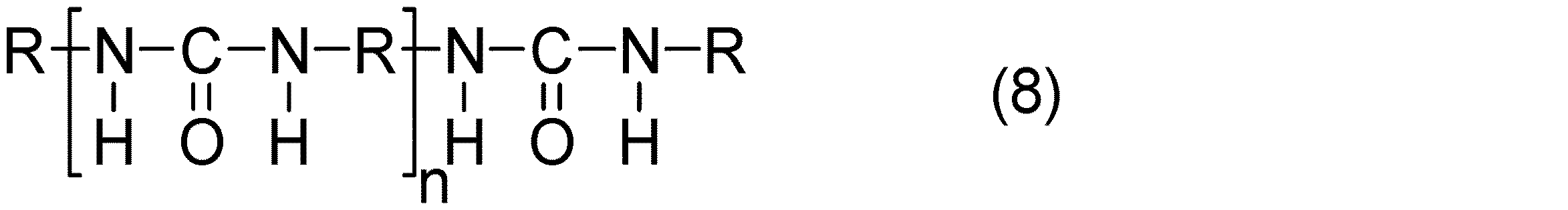
別の例では、第1の有機化合物は、式(1)又は式(2)に示すイソシアネートであることができ、第2の有機化合物は、以下の式(9)又は式(10)に示す水酸基を有する化合物であることができる。即ち、第1の有機化合物は、一官能性イソシアネート又は二官能性イソシアネートであることができ、第2の有機化合物は、水酸基を有する一官能性化合物又は水酸基を有する二官能性化合物であることができる。
![]()
![]()
![]()
![]()
式(9)及び式(10)において、Rは、アルキル基(直鎖状アルキル基若しくは環状アルキル基)等の飽和炭化水素基、アリール基等の不飽和炭化水素基、又はN、O、S、F、若しくはSi等のヘテロ原子を含む基である。ヘテロ原子を含む基は、その一部の元素がN、O、S、F、若しくはSi等で置換された飽和炭化水素基又は不飽和炭化水素基を含む。なお、式(1)及び式(2)においてRで示される原子団は、式(9)及び式(10)においてRで示される原子団と同一であってもよく、異なっていてもよい。水酸基を有する化合物は、アルコール又はフェノールである。第2の有機化合物であるアルコールとしては、例えばエチレングリコールが挙げられる。また、第2の有機化合物であるフェノールとしては、例えばヒドロキノンが挙げられる。 In formulas (9) and (10), R is a saturated hydrocarbon group such as an alkyl group (linear alkyl group or cyclic alkyl group), an unsaturated hydrocarbon group such as an aryl group, or N, O, S. , F, or a group containing a hetero atom such as Si. The group containing a heteroatom includes a saturated hydrocarbon group or an unsaturated hydrocarbon group in which some of the elements are substituted with N, O, S, F, Si or the like. The atomic group represented by R in the formulas (1) and (2) may be the same as or different from the atomic group represented by R in the formulas (9) and (10). The compound having a hydroxyl group is an alcohol or phenol. Examples of the alcohol, which is the second organic compound, include ethylene glycol. Further, as the phenol which is the second organic compound, for example, hydroquinone can be mentioned.
イソシアネートと水酸基を有する化合物との重合(重付加)によって得られる有機化合物としては、以下の式(11)〜式(15)に示すウレタン結合を有する化合物が挙げられる。式(11)に示す化合物は、式(1)に示す化合物と式(9)に示す化合物との重合により、生成される。式(12)に示す化合物は、式(1)に示す化合物と式(10)に示す化合物との重合により、生成される。式(13)に示す化合物は、式(2)に示す化合物と式(9)に示す化合物との重合により、生成される。式(14)に示す化合物は、式(2)に示す化合物と式(10)に示す化合物との重合により、生成される。また、式(15)に示す化合物は、式(14)に示すポリマーの両末端をそれぞれ、イソシアネート基を有するモノマー(例えば式(1)に示す化合物)、水酸基を有するモノマー(例えば式(9)に示す化合物)で終端させた構造を有する。なお、式(14)及び式(15)において、nは2以上の整数である。
更に別の例では、第1の有機化合物は、以下の式(16)又は式(17)に示すカルボン酸であることができ、第2の有機化合物は、式(3)又は式(4)に示すアミンであることができる。即ち、第1の有機化合物は、一官能性カルボン酸又は二官能性カルボン酸であることができ、第2の有機化合物は、一官能性アミン又は二官能性アミンであることができる。
![]()
![]()
![]()
![]()
式(16)及び式(17)において、Rは、アルキル基(直鎖状アルキル基若しくは環状アルキル基)等の飽和炭化水素基、アリール基等の不飽和炭化水素基、又はN、O、S、F、若しくはSi等のヘテロ原子を含む基である。ヘテロ原子を含む基は、その一部の元素がN、O、S、F、若しくはSi等で置換された飽和炭化水素基又は不飽和炭化水素基を含む。なお、式(3)及び式(4)においてRで示される原子団は、式(16)及び式(17)においてRで示される原子団と同一であってもよく、異なっていてもよい。第1の有機化合物であるカルボン酸としては、例えばテレフタル酸が挙げられる。 In formulas (16) and (17), R is a saturated hydrocarbon group such as an alkyl group (linear alkyl group or cyclic alkyl group), an unsaturated hydrocarbon group such as an aryl group, or N, O, S. , F, or a group containing a hetero atom such as Si. A group containing a heteroatom includes a saturated hydrocarbon group or an unsaturated hydrocarbon group in which some of its elements are substituted with N, O, S, F, Si or the like. The atomic group represented by R in the formulas (3) and (4) may be the same as or different from the atomic group represented by R in the formulas (16) and (17). Examples of the carboxylic acid which is the first organic compound include terephthalic acid.
カルボン酸とアミンとの重合(重縮合)によって得られる有機化合物としては、以下の式(18)〜式(22)に示すアミド結合を有する化合物、例えばポリアミドが挙げられる。式(18)に示す化合物は、式(16)に示す化合物と式(3)に示す化合物との重合により、生成される。式(19)に示す化合物は、式(16)に示す化合物と式(4)に示す化合物との重合により、生成される。式(20)に示す化合物は、式(17)に示す化合物と式(3)に示す化合物との重合により、生成される。式(21)に示す化合物は、式(17)に示す化合物と式(4)に示す化合物との重合により、生成される。また、式(22)に示す化合物は、式(21)に示すポリマーの両末端をそれぞれ、カルボキシル基を有するモノマー(例えば式(16)に示す化合物)、アミノ基を有するモノマー(例えば式(3)に示す化合物)で終端させた構造を有する。なお、式(21)及び式(22)において、nは2以上の整数である。カルボン酸とアミンとの重合反応では、水分子も生成される。生成された水分子は、減圧環境下においては処理空間から排気される。したがって、カルボン酸とアミンとの重合反応は、不可逆である。
![]()
![]()
なお、式(3)又は式(4)に示すアミンとの重合に用いられる第1の有機化合物は、以下の式(23)に示すカルボン酸ハロゲン化物であってもよい。式(23)において、Xは、F、Cl、Br、又はIである。また、式(23)においてRで示す原子団は、式(16)及び式(17)においてRで示す原子団と同じ原子団であり得る。
更に別の例では、第1の有機化合物は、式(16)又は式(17)に示すカルボン酸であることができ、第2の有機化合物は、式(9)又は式(10)に示す水酸基を有する化合物であることができる。即ち、第1の有機化合物は、一官能性カルボン酸又は二官能性カルボン酸であることができ、第2の有機化合物は、水酸基を有する一官能性化合物又は水酸基を有する二官能性化合物であることができる。なお、式(16)及び式(17)においてRで示される原子団は、式(9)及び式(10)においてRで示される原子団と同一であってもよく、異なっていてもよい。 In yet another example, the first organic compound can be the carboxylic acid of formula (16) or formula (17) and the second organic compound is of formula (9) or formula (10). It can be a compound having a hydroxyl group. That is, the first organic compound can be a monofunctional carboxylic acid or a bifunctional carboxylic acid, and the second organic compound is a monofunctional compound having a hydroxyl group or a bifunctional compound having a hydroxyl group. be able to. The atomic group represented by R in the formulas (16) and (17) may be the same as or different from the atomic group represented by R in the formulas (9) and (10).
カルボン酸と水酸基を有する化合物との重合(重縮合)によって得られる有機化合物としては、以下の式(24)〜式(28)に示すエステル結合を有する化合物、例えばポリエステルが挙げられる。式(24)に示す化合物は、式(16)に示す化合物と式(9)に示す化合物との重合により、生成される。式(25)に示す化合物は、式(16)に示す化合物と式(10)に示す化合物との重合により、生成される。式(26)に示す化合物は、式(17)に示す化合物と式(9)に示す化合物との重合により、生成される。式(27)に示す化合物は、式(17)に示す化合物と式(10)に示す化合物との重合により、生成される。また、式(28)に示す化合物は、式(27)に示すポリマーの両末端をそれぞれ、カルボキシル基を有するモノマー(例えば式(16)に示す化合物)、水酸基を有するモノマー(例えば式(9)に示す化合物)で終端させた構造を有する。なお、式(27)及び式(28)において、nは2以上の整数である。カルボン酸と水酸基を有する化合物との重合反応では、水分子も生成される。生成された水分子は、減圧環境下においては処理空間から排気される。したがって、カルボン酸と水酸基を有する化合物との重合反応は、不可逆である。
![]()
![]()
![]()
![]()
なお、式(9)又は式(10)に示す水酸基を有する化合物との重合に用いられる第1の有機化合物は、上記の式(23)に示すカルボン酸ハロゲン化物であってもよい。 The first organic compound used for polymerization with the compound having a hydroxyl group represented by the formula (9) or the formula (10) may be a carboxylic acid halide represented by the above formula (23).
更に別の例では、第1の有機化合物は、以下の式(29)又は式(30)に示す無水カルボン酸であることができ、第2の有機化合物は、式(3)又は式(4)に示すアミンであることができる。
式(29)及び式(30)において、Rは、アルキル基(直鎖状アルキル基若しくは環状アルキル基)等の飽和炭化水素基、アリール基等の不飽和炭化水素基、又はN、O、S、F、若しくはSi等のヘテロ原子を含む基である。ヘテロ原子を含む基は、その一部の元素がN、O、S、F、若しくはSi等で置換された飽和炭化水素基又は不飽和炭化水素基を含む。なお、式(29)及び式(30)においてRで示される原子団は、式(3)及び式(4)においてRで示される原子団と同一であってもよく、異なっていてもよい。第1の有機化合物である無水カルボン酸としては、例えば無水ピロメリット酸が挙げられる。 In formulas (29) and (30), R is a saturated hydrocarbon group such as an alkyl group (linear alkyl group or cyclic alkyl group), an unsaturated hydrocarbon group such as an aryl group, or N, O, S. , F, or a group containing a hetero atom such as Si. A group containing a heteroatom includes a saturated hydrocarbon group or an unsaturated hydrocarbon group in which some of its elements are substituted with N, O, S, F, Si or the like. The atomic group represented by R in the formulas (29) and (30) may be the same as or different from the atomic group represented by R in the formulas (3) and (4). Examples of the carboxylic acid anhydride as the first organic compound include pyromellitic anhydride.
無水カルボン酸とアミンとの重合によって得られる有機化合物としては、以下の式(31)又は式(32)に示すイミド化合物が挙げられる。式(31)に示す化合物は、式(29)に示す化合物と式(3)に示す化合物との重合により、生成される。式(32)に示す化合物は、式(30)に示す化合物と式(4)に示す化合物との重合により、生成される。なお、式(31)及び式(32)において、nは2以上の整数である。無水カルボン酸とアミンとの重合反応では、水分子も生成される。生成された水分子は、減圧環境下においては処理空間から排気される。したがって、無水カルボン酸とアミンとの重合反応は、不可逆である。なお、無水カルボン酸とアミンとの重合においては、一官能性無水カルボン酸、二官能性の無水カルボン酸、一官能性アミン、及び二官能性アミンを用いてもよい。
方法MTでは、次いで、基板Wがチャンバ11の中に搬入されて、支持台16上に載置される。基板Wは、静電チャック20によって保持される。
In the method MT, the substrate W is then carried into the
次いで、方法MTでは、工程ST2が実行される。工程ST2の実行時には、シャッターSHは、隔壁14の開口を閉じている。工程ST2では、基板Wの有機領域ORがエッチングされる。有機領域ORは、チャンバ11内(第1空間S1の中)でプラズマからの化学種によってエッチングされる。
Then, in the method MT, step ST2 is executed. When the step ST2 is executed, the shutter SH closes the opening of the
工程ST2では、内部空間S(第1空間S1)に処理ガスが供給される。処理ガスは、有機領域ORをエッチングし得るガスである限り、任意のガスを含み得る。処理ガスは、酸素含有ガスを含み得る。酸素含有ガスは、酸素ガス(O2ガス)、COガス、又はCO2ガスであり得る。或いは、処理ガスは、水素ガス(H2ガス)及び窒素ガス(N2ガス)の混合ガスであり得る。また、工程ST2では、内部空間Sの中の圧力が指定された圧力に設定されるよう、排気装置52が制御される。また、工程ST2では、処理ガスのプラズマを生成するために、第1の高周波電力が供給される。第2の高周波電力は供給されてもよく、供給されなくてもよい。
In step ST2, the processing gas is supplied to the internal space S (first space S1). The treatment gas may include any gas as long as it is a gas capable of etching the organic region OR. The processing gas may include an oxygen-containing gas. The oxygen-containing gas can be oxygen gas (O 2 gas), CO gas, or CO 2 gas. Alternatively, the processing gas may be a mixed gas of hydrogen gas (H 2 gas) and nitrogen gas (N 2 gas). Further, in the step ST2, the
工程ST2では、内部空間S(第1空間S1)の中で処理ガスのプラズマが生成される。工程ST2では、有機領域ORが、処理ガスのプラズマからの化学種により、図5に示すように、エッチングされる。プラズマからの化学種は、主としてラジカルを含み得る。プラズマからの化学種は、ラジカルに加えてイオンを含んでいてもよい。プラズマからの化学種は、基板Wの有機領域ORのプラズマエッチングのみならず、有機膜OFのエッチングにおいても消費される。有機膜OFは、基板Wが配置される領域WRの周囲で延在する表面上に形成されている。したがって、チャンバ11内の位置に依存した化学種の消費量のバラツキが抑制される。その結果、基板W上での位置に依存した化学種の密度のバラツキが抑制される。故に、方法MTによれば、有機領域ORのプラズマエッチングにおいて高い面内均一性が得られる。
In step ST2, plasma of the processing gas is generated in the internal space S (first space S1). In step ST2, the organic region OR is etched by the chemical species from the plasma of the processing gas, as shown in FIG. Species from plasma can contain primarily radicals. Species from the plasma may contain ions in addition to radicals. The chemical species from the plasma are consumed not only in the plasma etching of the organic region OR of the substrate W but also in the etching of the organic film OF. The organic film OF is formed on a surface extending around the region WR in which the substrate W is arranged. Therefore, the variation in the consumption of chemical species depending on the position in the
一実施形態においては、工程ST1及び工程ST2を含むシーケンスが繰り返されてもよい。シーケンスの繰り返しにより、複数の基板の有機領域ORがエッチングされてもよい。工程ST2の終了時には、図6に示すように、有機膜OFが上述した表面上に残される場合がある。一実施形態においては、次に実行されるシーケンスの前に、第1空間S1を画成する表面上の有機膜OFは除去される。このため、方法MTは、図1に示すように、工程ST3を含んでいてもよい。即ち、シーケンスは、工程ST1及び工程ST2に加えて工程ST3を含んでいてもよい。 In one embodiment, the sequence including step ST1 and step ST2 may be repeated. By repeating the sequence, the organic region OR of a plurality of substrates may be etched. At the end of step ST2, as shown in FIG. 6, the organic film OF may be left on the surface described above. In one embodiment, the organic film OF on the surface defining the first space S1 is removed prior to the next sequence performed. Therefore, the method MT may include step ST3 as shown in FIG. That is, the sequence may include step ST3 in addition to step ST1 and step ST2.
一実施形態の工程ST3では、プラズマクリーニングによって、有機膜OFが除去される。具体的には、内部空間S(第1空間S1)にクリーニングガスが供給される。クリーニングガスは、有機膜OFを除去し得るガスである限り、任意のガスを含み得る。クリーニングガスは、酸素含有ガスを含み得る。酸素含有ガスは、酸素ガス(O2ガス)、COガス、又はCO2ガスであり得る。或いは、クリーニングガスは、水素ガス(H2ガス)及び窒素ガス(N2ガス)の混合ガスであり得る。工程ST3では、内部空間Sの中の圧力が指定された圧力に設定されるよう、排気装置52が制御される。また、工程ST3では、クリーニングガスのプラズマを生成するために、第1の高周波電力が供給される。第2の高周波電力は供給されてもよく、供給されなくてもよい。工程ST3の実行時には、シャッターSHは、隔壁14の開口を閉じている。この実施形態の工程ST3では、クリーニングガスのプラズマからの活性種によって、図7に示すように、第1空間S1を画成する表面から有機膜OFが除去される。プラズマからの活性種は、第2空間S2には供給され難いので、第2空間S2を画成する表面上の有機膜OFは残される。なお、この実施形態の工程ST3の実行中には、支持台16(静電チャック20)上にダミー基板DWが載置されていてもよい。或いは、この実施形態の工程ST3の実行中には、支持台16(静電チャック20)上に物体が載置されていなくてもよい。
In step ST3 of one embodiment, the organic film OF is removed by plasma cleaning. Specifically, the cleaning gas is supplied to the internal space S (first space S1). The cleaning gas may contain any gas as long as it can remove the organic film OF. The cleaning gas may include an oxygen-containing gas. The oxygen-containing gas can be oxygen gas (O 2 gas), CO gas, or CO 2 gas. Alternatively, the cleaning gas may be a mixed gas of hydrogen gas (H 2 gas) and nitrogen gas (N 2 gas). In step ST3, the
別の実施形態の工程ST3は、有機膜OFが、イソシアネートとアミンとの重合により生成された有機化合物から構成されている場合、又は、イソシアネートと水酸基を有する化合物との重合により生成された有機化合物から構成されている場合に、適用可能である。この実施形態の工程ST3では、その表面上に有機膜OFが形成されている一つ以上の部品の各々が第3の温度範囲内の温度に加熱される。工程ST3の実行時には、シャッターSHは、隔壁14の開口を閉じている。この実施形態の工程ST3においては、例えば、隔壁14、上部電極30、部材32がそれぞれ、ヒータHT14、ヒータHT30、ヒータHT32によって第3の温度範囲内の温度に加熱される。フォーカスリングFR上にも有機膜OFが形成されている場合には、フォーカスリングFRはヒータHTFによって第3の温度範囲内の温度に加熱される。その結果、有機膜OFを構成する有機化合物の解重合が生じる。解重合によって生成された有機化合物の気体は、排気される。したがって、図8に示すように、内部空間Sを画成する表面から有機膜OFが除去される。
In step ST3 of another embodiment, the organic film OF is composed of an organic compound produced by polymerization of isocyanate and amine, or an organic compound produced by polymerization of isocyanate and a compound having a hydroxyl group. Applicable when composed of. In step ST3 of this embodiment, each of one or more parts having an organic film OF formed on the surface thereof is heated to a temperature within a third temperature range. When the step ST3 is executed, the shutter SH closes the opening of the
続く工程ST4では、停止条件が満たされるか否かが判定される。停止条件は、工程ST1及び工程ST2を含むシーケンスの実行回数が所定回数に達している場合に満たされていると判定される。工程ST4において停止条件が満たされていないと判定された場合には、工程ST1及び工程ST2を含むシーケンスが再び実行される。一方、工程ST4において停止条件が満たされていると判定された場合には、方法MTが終了する。 In the subsequent step ST4, it is determined whether or not the stop condition is satisfied. It is determined that the stop condition is satisfied when the number of executions of the sequence including the steps ST1 and ST2 reaches a predetermined number of times. If it is determined in step ST4 that the stop condition is not satisfied, the sequence including step ST1 and step ST2 is executed again. On the other hand, if it is determined in step ST4 that the stop condition is satisfied, the method MT ends.
以上、種々の実施形態について説明してきたが、上述した実施形態に限定されることなく種々の変形態様を構成可能である。例えば、方法MTは、プラズマ処理装置10以外のプラズマ処理装置を用いて実行されてもよい。そのようなプラズマ処理装置としては、誘導結合型のプラズマ処理装置、又は、マイクロ波といった表面波によりプラズマを生成するプラズマ処理装置が例示される。
Although various embodiments have been described above, various modifications can be configured without being limited to the above-described embodiments. For example, the method MT may be performed using a plasma processing device other than the
10…プラズマ処理装置、11…チャンバ、MT…方法、W…基板、OR…有機領域、OF…有機膜。 10 ... Plasma processing device, 11 ... Chamber, MT ... Method, W ... Substrate, OR ... Organic region, OF ... Organic film.
Claims (16)
プラズマ処理装置のチャンバ内の表面上に有機膜を形成する工程であり、該表面は、前記基板が前記プラズマ処理装置の前記チャンバ内で配置される領域の周囲で延在する、該工程と、
有機膜を形成する前記工程において前記表面上に形成された前記有機膜が存在する状態で、前記チャンバ内でプラズマからの化学種によって前記有機領域をエッチングする工程と、
を含み、
有機膜を形成する前記工程では、第1の有機化合物を含む第1のガス及び第2の有機化合物を含む第2のガスが前記チャンバ内に供給され、
前記有機膜は、前記第1の有機化合物と前記第2の有機化合物の重合により形成され、
前記チャンバはチャンバ本体を含み、該チャンバ本体は第1空間及び第2空間を含む内部空間を有し、該第1空間と該第2空間とは隔壁によって分けられており、
前記隔壁は、前記基板が前記第1空間と前記チャンバの外部との間でそれを介して搬送される開口と、該隔壁の該開口を開閉するシャッターと、を含み、
前記プラズマ処理装置は上部電極及び部材を含み、該上部電極は前記部材と共に前記チャンバ本体の上部開口を閉じており、
有機膜を形成する前記工程において、前記有機膜は、前記隔壁の表面、前記上部電極の表面、及び前記部材の表面の上に形成され、
前記有機膜を形成することは、前記シャッターが前記隔壁の前記開口を開いているときに行われる、
方法。 It is a method of etching the organic region of the substrate.
A step of forming an organic film on a surface in a chamber of a plasma processing apparatus, wherein the surface extends around an area in which the substrate is arranged in the chamber of the plasma processing apparatus.
In the step of forming the organic film, a step of etching the organic region with a chemical species from plasma in the chamber in a state where the organic film formed on the surface is present.
Including
In the step of forming the organic film, a first gas containing the first organic compound and a second gas containing the second organic compound are supplied into the chamber.
The organic film is formed by polymerizing the first organic compound and the second organic compound .
The chamber includes a chamber body, the chamber body has an internal space including a first space and a second space, and the first space and the second space are separated by a partition wall.
The partition wall comprises an opening through which the substrate is conveyed between the first space and the outside of the chamber, and a shutter that opens and closes the opening of the partition wall.
The plasma processing apparatus includes an upper electrode and a member, and the upper electrode closes the upper opening of the chamber body together with the member.
In the step of forming the organic film, the organic film is formed on the surface of the partition wall, the surface of the upper electrode, and the surface of the member.
The formation of the organic film is performed when the shutter opens the opening of the partition wall.
Method.
前記第2の温度範囲は、前記第1の温度範囲の下限よりも低く、前記第3の温度範囲は、前記第1の温度範囲の上限よりも高い、 The second temperature range is lower than the lower limit of the first temperature range, and the third temperature range is higher than the upper limit of the first temperature range.
請求項1に記載の方法。The method according to claim 1.
請求項2に記載の方法。The method according to claim 2.
プラズマ処理装置のチャンバ内の表面上に有機膜を形成する工程であり、該表面は、前記基板が前記プラズマ処理装置の前記チャンバ内で配置される領域の周囲で延在する、該工程と、 A step of forming an organic film on a surface in a chamber of a plasma processing apparatus, wherein the surface extends around an area in which the substrate is arranged in the chamber of the plasma processing apparatus.
有機膜を形成する前記工程において前記表面上に形成された前記有機膜が存在する状態で、前記チャンバ内でプラズマからの化学種によって前記有機領域をエッチングする工程と、 In the step of forming the organic film, a step of etching the organic region with a chemical species from plasma in the chamber in a state where the organic film formed on the surface is present.
を含み、Including
有機膜を形成する前記工程では、第1の有機化合物を含む第1のガス及び第2の有機化合物を含む第2のガスが前記チャンバ内に供給され、 In the step of forming the organic film, a first gas containing the first organic compound and a second gas containing the second organic compound are supplied into the chamber.
前記有機膜は、前記第1の有機化合物と前記第2の有機化合物の重合により形成され、 The organic film is formed by polymerizing the first organic compound and the second organic compound.
有機膜を形成する前記工程において、前記基板が配置される前記領域の周囲で延在する前記表面が、第1の温度範囲内の温度に加熱され、前記基板が配置される前記領域が、第2の温度範囲又は第3の温度範囲内の温度に設定され、 In the step of forming the organic film, the surface extending around the region where the substrate is arranged is heated to a temperature within the first temperature range, and the region where the substrate is arranged is the first. Set to a temperature within the 2nd or 3rd temperature range,
前記第2の温度範囲は、前記第1の温度範囲の下限よりも低く、前記第3の温度範囲は、前記第1の温度範囲の上限よりも高い、 The second temperature range is lower than the lower limit of the first temperature range, and the third temperature range is higher than the upper limit of the first temperature range.
方法。Method.
請求項4に記載の方法。 The first temperature range is 0 ° C. or higher and 150 ° C. or lower, and the third temperature range is 250 ° C. or higher and 400 ° C. or lower.
The method according to claim 4.
有機膜を形成する前記工程において、前記表面上で選択的に前記重合が生じるように、前記ヒータによって前記一つ以上の部品が加熱される、請求項1〜5の何れか一項に記載の方法。 A heater is provided in each of one or more parts that define the surface of the plasma processing apparatus.
The step according to any one of claims 1 to 5, wherein the heater heats the one or more parts so that the polymerization selectively occurs on the surface in the step of forming the organic film. Method.
該方法は、前記有機領域をエッチングする前記工程の後、有機膜を形成する前記工程の前に、プラズマクリーニングによって前記有機膜を除去する工程を更に含む、
請求項1〜6の何れか一項に記載の方法。 The sequence including the step of forming the organic film and the step of etching the organic region is repeated.
The method further comprises the step of removing the organic film by plasma cleaning after the step of etching the organic region and before the step of forming the organic film.
The method according to any one of claims 1 to 6.
該方法は、前記有機領域をエッチングする前記工程の後、有機膜を形成する前記工程の前に、前記有機膜の解重合により前記有機膜を除去する工程を更に含む、
請求項1〜6の何れか一項に記載の方法。 The sequence including the step of forming the organic film and the step of etching the organic region is repeated.
The method further comprises a step of removing the organic film by depolymerization of the organic film after the step of etching the organic region and before the step of forming the organic film.
The method according to any one of claims 1 to 6.
有機膜を形成する前記工程において、前記有機膜は、前記第1空間を画成する表面上に形成される、
請求項1〜9の何れか一項に記載の方法。 The chamber has an internal space including a first space and a second space, and the first space and the second space are separated by a partition wall.
In the step of forming the organic film, the organic film is formed on the surface defining the first space.
The method according to any one of claims 1 to 9.
該方法は、有機膜を形成する前記工程と前記有機領域をエッチングする前記工程との間に、前記基板を前記チャンバ内に搬送する工程を更に含む、
請求項1〜11の何れか一項に記載の方法。 The step of forming the organic film is performed when the substrate is not arranged in the chamber.
The method further comprises the step of transporting the substrate into the chamber between the step of forming the organic film and the step of etching the organic region.
The method according to any one of claims 1 to 11.
Priority Applications (4)
| Application Number | Priority Date | Filing Date | Title |
|---|---|---|---|
| JP2018082127A JP6910319B2 (en) | 2018-04-23 | 2018-04-23 | How to etch the organic region |
| TW108113146A TWI814810B (en) | 2018-04-23 | 2019-04-16 | Method for etching organic region |
| KR1020190045991A KR20190123225A (en) | 2018-04-23 | 2019-04-19 | Method for etching organic region |
| US16/390,326 US10903085B2 (en) | 2018-04-23 | 2019-04-22 | Method for etching organic region |
Applications Claiming Priority (1)
| Application Number | Priority Date | Filing Date | Title |
|---|---|---|---|
| JP2018082127A JP6910319B2 (en) | 2018-04-23 | 2018-04-23 | How to etch the organic region |
Publications (3)
| Publication Number | Publication Date |
|---|---|
| JP2019192725A JP2019192725A (en) | 2019-10-31 |
| JP2019192725A5 JP2019192725A5 (en) | 2021-03-25 |
| JP6910319B2 true JP6910319B2 (en) | 2021-07-28 |
Family
ID=68236572
Family Applications (1)
| Application Number | Title | Priority Date | Filing Date |
|---|---|---|---|
| JP2018082127A Active JP6910319B2 (en) | 2018-04-23 | 2018-04-23 | How to etch the organic region |
Country Status (4)
| Country | Link |
|---|---|
| US (1) | US10903085B2 (en) |
| JP (1) | JP6910319B2 (en) |
| KR (1) | KR20190123225A (en) |
| TW (1) | TWI814810B (en) |
Families Citing this family (1)
| Publication number | Priority date | Publication date | Assignee | Title |
|---|---|---|---|---|
| US20210195726A1 (en) * | 2019-12-12 | 2021-06-24 | James Andrew Leskosek | Linear accelerator using a stacked array of cyclotrons |
Family Cites Families (12)
| Publication number | Priority date | Publication date | Assignee | Title |
|---|---|---|---|---|
| JPH05243167A (en) * | 1992-02-28 | 1993-09-21 | Sony Corp | Manufacture of semiconductor device |
| JP3258240B2 (en) * | 1996-09-10 | 2002-02-18 | 株式会社日立製作所 | Etching method |
| JP2000195841A (en) * | 1998-12-28 | 2000-07-14 | Fujitsu Ltd | Method and apparatus for etching |
| JP4701776B2 (en) | 2005-03-25 | 2011-06-15 | 東京エレクトロン株式会社 | Etching method and etching apparatus |
| US7674393B2 (en) | 2005-03-25 | 2010-03-09 | Tokyo Electron Limited | Etching method and apparatus |
| US7578258B2 (en) * | 2006-03-03 | 2009-08-25 | Lam Research Corporation | Methods and apparatus for selective pre-coating of a plasma processing chamber |
| JP2011151263A (en) * | 2010-01-22 | 2011-08-04 | Tokyo Electron Ltd | Etching method, etching device, and ring member |
| JP5198611B2 (en) * | 2010-08-12 | 2013-05-15 | 株式会社東芝 | Gas supply member, plasma processing apparatus, and method for forming yttria-containing film |
| JP6462477B2 (en) * | 2015-04-27 | 2019-01-30 | 東京エレクトロン株式会社 | Method for processing an object |
| JP6537473B2 (en) * | 2015-10-06 | 2019-07-03 | 東京エレクトロン株式会社 | Method of processing an object |
| JP6697416B2 (en) * | 2016-07-07 | 2020-05-20 | 信越化学工業株式会社 | Resist underlayer film material, pattern forming method, resist underlayer film forming method, and compound for resist underlayer film material |
| JP6465189B2 (en) * | 2016-07-21 | 2019-02-06 | 東京エレクトロン株式会社 | Semiconductor device manufacturing method and vacuum processing apparatus |
-
2018
- 2018-04-23 JP JP2018082127A patent/JP6910319B2/en active Active
-
2019
- 2019-04-16 TW TW108113146A patent/TWI814810B/en active
- 2019-04-19 KR KR1020190045991A patent/KR20190123225A/en not_active Application Discontinuation
- 2019-04-22 US US16/390,326 patent/US10903085B2/en active Active
Also Published As
| Publication number | Publication date |
|---|---|
| TW202002069A (en) | 2020-01-01 |
| US10903085B2 (en) | 2021-01-26 |
| US20190326106A1 (en) | 2019-10-24 |
| KR20190123225A (en) | 2019-10-31 |
| JP2019192725A (en) | 2019-10-31 |
| TWI814810B (en) | 2023-09-11 |
Similar Documents
| Publication | Publication Date | Title |
|---|---|---|
| JP6799550B2 (en) | How to clean parts of plasma processing equipment | |
| CN101410941B (en) | Post-etch treatment system for removing residue on a substrate | |
| CN110010464B (en) | Method for processing substrate | |
| JP6799549B2 (en) | How to clean parts of plasma processing equipment | |
| WO2007117741A2 (en) | A reduced contaminant gas injection system and method of using | |
| US20210082713A1 (en) | Etching method, plasma processing apparatus, and substrate processing system | |
| US10923332B2 (en) | Plasma processing method | |
| US20230010069A1 (en) | Apparatus for substrate processing | |
| JP6910319B2 (en) | How to etch the organic region | |
| CN111048389A (en) | Plasma processing method and plasma processing apparatus | |
| US20200144028A1 (en) | Plasma processing apparatus and plasma processing method | |
| TW202247280A (en) | Chamber and methods of treating a substrate after exposure to radiation | |
| JP7308110B2 (en) | METHOD AND PLASMA PROCESSING APPARATUS FOR ETCHING SILICON OXIDE FILM | |
| CN112509920A (en) | Etching method, plasma processing apparatus, and substrate processing system | |
| JP7493400B2 (en) | Etching method, plasma processing apparatus, and substrate processing system | |
| WO2024054537A1 (en) | Vacuum bake for euv lithography | |
| JP2011049365A (en) | Plasma processing method |
Legal Events
| Date | Code | Title | Description |
|---|---|---|---|
| A521 | Request for written amendment filed |
Free format text: JAPANESE INTERMEDIATE CODE: A523 Effective date: 20210128 |
|
| A621 | Written request for application examination |
Free format text: JAPANESE INTERMEDIATE CODE: A621 Effective date: 20210128 |
|
| A871 | Explanation of circumstances concerning accelerated examination |
Free format text: JAPANESE INTERMEDIATE CODE: A871 Effective date: 20210128 |
|
| A975 | Report on accelerated examination |
Free format text: JAPANESE INTERMEDIATE CODE: A971005 Effective date: 20210329 |
|
| A131 | Notification of reasons for refusal |
Free format text: JAPANESE INTERMEDIATE CODE: A131 Effective date: 20210406 |
|
| A521 | Request for written amendment filed |
Free format text: JAPANESE INTERMEDIATE CODE: A523 Effective date: 20210517 |
|
| TRDD | Decision of grant or rejection written | ||
| A01 | Written decision to grant a patent or to grant a registration (utility model) |
Free format text: JAPANESE INTERMEDIATE CODE: A01 Effective date: 20210608 |
|
| A61 | First payment of annual fees (during grant procedure) |
Free format text: JAPANESE INTERMEDIATE CODE: A61 Effective date: 20210706 |
|
| R150 | Certificate of patent or registration of utility model |
Ref document number: 6910319 Country of ref document: JP Free format text: JAPANESE INTERMEDIATE CODE: R150 |