JP6707808B2 - Antennas, electronic devices and watches - Google Patents
Antennas, electronic devices and watches Download PDFInfo
- Publication number
- JP6707808B2 JP6707808B2 JP2015061212A JP2015061212A JP6707808B2 JP 6707808 B2 JP6707808 B2 JP 6707808B2 JP 2015061212 A JP2015061212 A JP 2015061212A JP 2015061212 A JP2015061212 A JP 2015061212A JP 6707808 B2 JP6707808 B2 JP 6707808B2
- Authority
- JP
- Japan
- Prior art keywords
- ribbon
- radiating element
- antenna
- ground plate
- circuit board
- Prior art date
- Legal status (The legal status is an assumption and is not a legal conclusion. Google has not performed a legal analysis and makes no representation as to the accuracy of the status listed.)
- Active
Links
Images


Classifications
-
- H—ELECTRICITY
- H01—ELECTRIC ELEMENTS
- H01Q—ANTENNAS, i.e. RADIO AERIALS
- H01Q1/00—Details of, or arrangements associated with, antennas
- H01Q1/27—Adaptation for use in or on movable bodies
- H01Q1/273—Adaptation for carrying or wearing by persons or animals
-
- G—PHYSICS
- G04—HOROLOGY
- G04R—RADIO-CONTROLLED TIME-PIECES
- G04R20/00—Setting the time according to the time information carried or implied by the radio signal
- G04R20/02—Setting the time according to the time information carried or implied by the radio signal the radio signal being sent by a satellite, e.g. GPS
- G04R20/04—Tuning or receiving; Circuits therefor
-
- G—PHYSICS
- G04—HOROLOGY
- G04R—RADIO-CONTROLLED TIME-PIECES
- G04R60/00—Constructional details
- G04R60/06—Antennas attached to or integrated in clock or watch bodies
- G04R60/10—Antennas attached to or integrated in clock or watch bodies inside cases
-
- G—PHYSICS
- G04—HOROLOGY
- G04R—RADIO-CONTROLLED TIME-PIECES
- G04R60/00—Constructional details
- G04R60/06—Antennas attached to or integrated in clock or watch bodies
- G04R60/10—Antennas attached to or integrated in clock or watch bodies inside cases
- G04R60/12—Antennas attached to or integrated in clock or watch bodies inside cases inside metal cases
-
- H—ELECTRICITY
- H01—ELECTRIC ELEMENTS
- H01Q—ANTENNAS, i.e. RADIO AERIALS
- H01Q1/00—Details of, or arrangements associated with, antennas
- H01Q1/48—Earthing means; Earth screens; Counterpoises
-
- H—ELECTRICITY
- H01—ELECTRIC ELEMENTS
- H01Q—ANTENNAS, i.e. RADIO AERIALS
- H01Q9/00—Electrically-short antennas having dimensions not more than twice the operating wavelength and consisting of conductive active radiating elements
- H01Q9/04—Resonant antennas
- H01Q9/30—Resonant antennas with feed to end of elongated active element, e.g. unipole
- H01Q9/42—Resonant antennas with feed to end of elongated active element, e.g. unipole with folded element, the folded parts being spaced apart a small fraction of the operating wavelength
Landscapes
- Physics & Mathematics (AREA)
- General Physics & Mathematics (AREA)
- Engineering & Computer Science (AREA)
- Radar, Positioning & Navigation (AREA)
- Remote Sensing (AREA)
- Electric Clocks (AREA)
- Aerials With Secondary Devices (AREA)
- Details Of Aerials (AREA)
Description
本発明は、アンテナ及びアンテナを備える電子機器に関する。 The present invention relates to an antenna and an electronic device including the antenna.
腕時計など小型の筐体にGPS(Global Positioning System)受信機を組込む場合、当該受信機に用いられるアンテナについても体積を極力小さくする必要がある。したがって、回路基板をGND(グラウンド)として使用したグラウンドプレーンアンテナが各社製品にて採用されている。しかしながら、グラウンドプレーンアンテナは、例えば腕時計を腕に装着した時に、電波が腕で吸収され、腕に装着しない状態と比較して感度が低下し易い。そこで、平面部と、前記回路基板を保持する保持部とを有する導電性の保持部材によって前記回路基板を保持し、GNDを実質的に大きくする手法が採用されている(例えば、特許文献1)。 When a GPS (Global Positioning System) receiver is incorporated in a small case such as a wristwatch, it is necessary to make the volume of the antenna used in the receiver as small as possible. Therefore, the ground plane antenna using the circuit board as GND (ground) is adopted in each company's product. However, when the wristwatch is worn on the wrist, radio waves are absorbed by the ground plane antenna, and the sensitivity of the ground plane antenna is likely to be lower than that when the wristplane is not worn on the wrist. Therefore, a method is adopted in which the circuit board is held by a conductive holding member having a flat surface portion and a holding portion that holds the circuit board, and the GND is substantially increased (for example, Patent Document 1). .
しかしながら、特許文献1の前記保持部材は、前記回路基板だけでなく、前記回路基板の周囲の部材を取り囲むようにして取り付けられるため、構造的に採用し得ない場合がある。
本発明は上述した事情に鑑みてなされたものであり、腕等に近い場所で使用される場合でも感度の低下が少ないアンテナ及び当該アンテナを備えた電子機器を提供することを解決課題とする。
However, since the holding member of
The present invention has been made in view of the above-mentioned circumstances, and an object of the present invention is to provide an antenna and an electronic device including the antenna, in which the sensitivity is not significantly reduced even when the antenna is used near an arm or the like.
本発明は、上述の課題の少なくとも一部を解決するためになされたものであり、以下の形態または適用例として実現することが可能である。 The present invention has been made to solve at least a part of the problems described above, and can be realized as the following modes or application examples.
[適用例1]本適用例に係るアンテナは、第1の放射素子と、前記第1の放射素子が接地する接地点を有するグラウンド板と、接地点においてグラウンド板に接地された第1の放射素子と、前記接地点を電気的に共有する位置において前記グラウンド板に接地された第2の放射素子と、を含み、前記第2の放射素子の配置は、前記第1の放射素子による前記グラウンド板における電流の方向に沿った配置となっている。 Application Example 1 An antenna according to this application example includes a first radiating element, a ground plate having a ground point at which the first radiating element is grounded, and a first radiation grounded to the ground plate at the ground point. An element and a second radiating element that is grounded to the ground plate at a position that electrically shares the ground point, and the second radiating element is arranged by the first radiating element. The arrangement is along the direction of current flow in the plate.
本適用例によれば、アンテナは、グラウンド板において接地点を電気的に共有する第1の放射素子と第2の放射素子とを含み、第2の放射素子の配置は、第1の放射素子によるグラウンド板における電流の方向に沿った配置となっている。したがって、グラウンド板を十分に大きくできない場合であっても、実際のグラウンド板よりも大きいグラウンド板における第1の放射素子による電流分布が、第2の放射素子によって再現されることになる。したがって、アンテナの指向性がグラウンドプレーンアンテナの指向性、つまり、グラウンド板に平行な方向の指向性に近づくので、アンテナが腕等に近い場所に位置する場合であっても、腕等によって吸収される電力を減少させ、アンテナの感度の低下を防ぐことができる。 According to this application example, the antenna includes the first radiating element and the second radiating element that electrically share the ground point on the ground plate, and the arrangement of the second radiating element is the first radiating element. Is arranged along the direction of the current in the ground plate. Therefore, even if the ground plate cannot be made sufficiently large, the current distribution by the first radiating element in the ground plate larger than the actual ground plate is reproduced by the second radiating element. Therefore, the directivity of the antenna approaches the directivity of the ground plane antenna, that is, the directivity in the direction parallel to the ground plate, so even if the antenna is located near the arm, it is absorbed by the arm. Power can be reduced and the antenna sensitivity can be prevented from lowering.
[適用例2]上記適用例のアンテナにおいて、前記第2の放射素子は、前記グウランド板に対して前記第1の放射素子と対称な位置にあってもよい。 Application Example 2 In the antenna of the above application example, the second radiating element may be positioned symmetrically with respect to the first radiating element with respect to the gourland plate.
上記適用例によれば、グラウンド板を十分に大きくできない場合であっても、十分に大きいグラウンド板に対して第1の放射素子と対称の位置に作られる影像が、第2の放射素子として実際に存在することになる。したがって、十分に大きいグラウンド板上の第1の放射素子による電流分布が、第2の放射素子によって再現されることになる。したがって、アンテナの指向性がグラウンドプレーンアンテナの指向性、つまり、グラウンド板に平行な方向の指向性に近づくので、アンテナが腕等に近い場所に位置する場合であっても、腕等によって吸収される電力を減少させ、アンテナの感度の低下を防ぐ。 According to the above application example, even when the ground plate cannot be made sufficiently large, the image formed at a position symmetrical to the first radiating element with respect to the sufficiently large ground plate is actually used as the second radiating element. Will exist in. Therefore, the sufficiently large current distribution by the first radiating element on the ground plate is reproduced by the second radiating element. Therefore, the directivity of the antenna approaches the directivity of the ground plane antenna, that is, the directivity in the direction parallel to the ground plate, so even if the antenna is located near the arm, it is absorbed by the arm. The power consumption is reduced and the antenna sensitivity is prevented from decreasing.
[適用例3]上記適用例のアンテナにおいて、前記第2の放射素子と前記第1の放射素子とは、前記グウランド板の同じ面側の位置にあってもよい。 Application Example 3 In the antenna of the application example described above, the second radiating element and the first radiating element may be located on the same surface side of the Guland plate.
上記適用例によれば、グラウンド板を十分に大きくできない場合であっても、十分に大きいグラウンド板上の第1の放射素子による電流分布が、第2の放射素子によって再現されることになる。したがって、アンテナの指向性がグラウンドプレーンアンテナの指向性に近づき、アンテナが腕等に近い場所に位置する場合であっても、腕等によって吸収される電力を減少させ、アンテナの感度の低下を防ぐ。 According to the application example described above, even when the ground plate cannot be made sufficiently large, the current distribution due to the first radiating element on the ground plate which is sufficiently large is reproduced by the second radiating element. Therefore, even when the directivity of the antenna approaches the directivity of the ground plane antenna and the antenna is located near the arm or the like, the power absorbed by the arm or the like is reduced and the antenna sensitivity is prevented from lowering. ..
[適用例4]上記適用例のアンテナにおいて、前記第1の放射素子および前記第2の放射素子は、前記グラウンド板に対する平面視(グラウンド板の平面に対し垂直な方向から見た状態)において円弧状であってもよい。 Application Example 4 In the antenna of the above application example, the first radiating element and the second radiating element are circles in a plan view with respect to the ground plate (a state viewed from a direction perpendicular to the plane of the ground plate). It may be arcuate.
上記適用例によれば、いずれの放射素子も円弧状なので、例えば円筒形状の筐体にアンテナを収納する場合等に、アンテナを筐体の形状に合わせて配置しやすくかつ、第2の放射素子によってアンテナの感度の低下を防ぐことができる。 According to the application example described above, since all the radiating elements are arcuate, it is easy to arrange the antenna in conformity with the shape of the housing when, for example, housing the antenna in a cylindrical housing. This can prevent the sensitivity of the antenna from decreasing.
[適用例5]上記適用例のアンテナにおいて、前記第2の放射素子は、屈曲部を含んでいてもよい。 Application Example 5 In the antenna of the above application example, the second radiating element may include a bent portion.
上記適用例によれば、第2の放射素子が屈曲部を含んでいても、接地点に接続された第2の放射素子の一端部から見た第2の放射素子の他端部の位置が、グラウンド板における第1の放射素子による電流の方向に沿っていれば、第2の放射素子全体として、十分に大きいグラウンド板上の第1の放射素子による電流分布を再現する。したがって、第2の放射素子の配置箇所における形状的な制約がある場合でも、アンテナの感度の低下を防ぐ。 According to the application example described above, even if the second radiating element includes the bent portion, the position of the other end of the second radiating element seen from one end of the second radiating element connected to the ground point is If the second radiating element as a whole is arranged along the direction of the current of the first radiating element on the ground plate, a sufficiently large current distribution by the first radiating element on the ground plate is reproduced. Therefore, even if there is a shape restriction in the location where the second radiating element is arranged, the antenna sensitivity is prevented from being lowered.
[適用例6]上記適用例のアンテナにおいて、前記第1の放射素子及び前記第2の放射素子の等価電気長は1/4波長であることが好ましい。 Application Example 6 In the antenna of the above application example, it is preferable that the equivalent electrical lengths of the first radiating element and the second radiating element are ¼ wavelength.
上記適用例によれば、第1の放射素子と第2の放射素子とを合わせた等価電気長が1/2波長となり、本発明のアンテナを1/2波長で動作させることができる。 According to the application example described above, the equivalent electrical length of the first radiating element and the second radiating element combined is ½ wavelength, and the antenna of the present invention can be operated at ½ wavelength.
[適用例7]本適用例に係る電子機器は、第1の放射素子と、前記第1の放射素子が接地する接地点を有するグラウンド板と、前記接地点を電気的に共有する位置において前記グラウンド板に接地された第2の放射素子と、を含み、第2の放射素子の配置は、前記第1の放射素子による前記グラウンド板を流れる電流の方向に沿った配置となっている。 Application Example 7 An electronic device according to this application example is configured such that the first radiating element, a ground plate having a ground point at which the first radiating element is grounded, and the ground point electrically share the ground point. A second radiating element grounded to the ground plate, and the second radiating element is arranged along the direction of the current flowing through the ground plate by the first radiating element.
上記適用例によれば、グラウンド板を十分に大きくできない場合であっても、十分に大きいグラウンド板に対して第1の放射素子と対称の位置に作られる影像が、第2の放射素子として実際に存在することになる。したがって、十分に大きいグラウンド板上の第1の放射素子による電流分布が、第2の放射素子によって再現されることになる。したがって、アンテナの指向性がグラウンドプレーンアンテナの指向性、つまり、グラウンド板に平行な方向の指向性に近づくので、アンテナが腕等に近い場所に位置する場合であっても、腕等によって吸収される電力を減少させ、アンテナの感度の低下を防ぎ、良好な動作を行う。なお、電子機器は、腕時計型の電子時計、ランニングウォッチ、腕時計型の心拍計等の腕時計型の電子機器の他、イヤホン型のGPS機器、スマートフォン等の電子端末、及びヘッドマウントディスプレイ等の各種電子機器を含む概念である。 According to the above application example, even when the ground plate cannot be made sufficiently large, the image formed at the position symmetrical to the first radiating element with respect to the sufficiently large ground plate is actually used as the second radiating element. Will exist in. Therefore, the sufficiently large current distribution by the first radiating element on the ground plate is reproduced by the second radiating element. Therefore, the directivity of the antenna approaches the directivity of the ground plane antenna, that is, the directivity in the direction parallel to the ground plate, so even if the antenna is located near the arm, it is absorbed by the arm. The power consumption is reduced, the sensitivity of the antenna is prevented from decreasing, and good operation is performed. The electronic devices include wristwatch-type electronic devices such as wristwatch-type electronic timepieces, running watches, wristwatch-type heart rate monitors, earphone-type GPS devices, electronic terminals such as smartphones, and various electronic devices such as head-mounted displays. It is a concept that includes equipment.
[適用例8]本適用例の電子機器において、表示部と、前記表示部および前記アンテナを収容し、裏蓋を含むケースと、金属を含む無給電素子と、を含み、前記無給電素子の位置は、前記表示部に対して前記裏蓋とは反対側であり、前記第1の放射素子の位置は、前記無給電子前記裏蓋との間であるようにしてもよい。 Application Example 8 In the electronic device of this application example, a display unit, a case that houses the display unit and the antenna, and includes a case back, and a parasitic element that includes a metal are provided. The position may be on the opposite side of the display unit from the back cover, and the position of the first radiating element may be between the unpaid electron and the back cover.
上記適用例によれば、無給電素子と第1の放射素子とを電磁界的に結合させることにより、グラウンド板から受信面までの間隔を大きくすることができ、アンテナの放射効率が改善される。また、無給電素子をアンテナの一部として利用するため、無給電素子が無い場合と比較して第1の放射素子の体積を小さくできる。 According to the application example described above, the parasitic element and the first radiating element are electromagnetically coupled to each other, so that the distance from the ground plate to the receiving surface can be increased, and the radiation efficiency of the antenna is improved. . Further, since the parasitic element is used as a part of the antenna, the volume of the first radiating element can be reduced as compared with the case where there is no parasitic element.
[適用例9] 本適用例の電子機器において、前記グラウンド板は電子機器の回路基板であってもよい。 Application Example 9 In the electronic device of the application example, the ground plate may be a circuit board of the electronic device.
上記適用例によれば、電子機器に用いられる回路基板をアンテナの構成要素であるグラウンド板として用いるので、回路基板の他にグラウンド板を設ける場合と比較して、構成部品の点数を少なくすることができる。 According to the above application example, since the circuit board used in the electronic device is used as the ground plate which is a component of the antenna, the number of constituent parts can be reduced as compared with the case where the ground plate is provided in addition to the circuit board. You can
以下、添付の図面を参照しながら本発明に係る好適な実施の形態を説明する。図面において、各部の寸法及び縮尺は、実際のものと適宜に異なる。また、以下に述べる実施の形態は、本発明の好適な具体例であるから、技術的に好ましい種々の限定が付されているが、本発明の範囲は、以下の説明において特に本発明を限定する旨の記載がない限り、これらの形態に限られるものではない。 Hereinafter, preferred embodiments of the present invention will be described with reference to the accompanying drawings. In the drawings, the size and scale of each part may be different from the actual one. Further, the embodiment described below is a preferred specific example of the present invention, so various technically preferable limitations are attached, but the scope of the present invention particularly limits the present invention in the following description. Unless stated to the effect, it is not limited to these forms.
<第1実施形態>
A:アンテナ内蔵式電子機器の機構的な構成
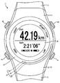
図1に示すように、本実施形態の電子機器1は、ユーザの手首に装着される腕時計型のランニングウォッチであり、上空にある数個のGPS衛星100から送信される衛星信号(GPS信号)をGPS受信機で受信し、現在の位置を算出することが可能なGPS機能を内蔵する。電子機器1は、GPS信号を用いて算出される位置情報と時刻情報により、例えばランニング時に走った距離・速度や経路を測定することができ、ユーザの運動を支援できる。
<First Embodiment>
A: Mechanical Configuration of Electronic Device with Built-in Antenna As shown in FIG. 1, the
電子機器1は、図2ないし図4にも示すように、外装ケース2と、バンド3とを備える。なお、電子機器1において、時刻や測定データをユーザが視認する側を表面側、腕に装着される側を裏面側とする。また、電子機器1において、表示された文字または数字の上方向を12時側、下方向を6時側とする。これは、腕時計型の電子機器1を一般的なアナログ式の腕時計に見立て、アナログ式の腕時計における時刻表示に合わせた表現である。そして、電子機器1の裏面側および表面側を結ぶ方向(図3に示す矢印A1の方向)を電子機器1の厚さ方向A1とする。
The
外装ケース2は、ケース本体11と裏蓋12とを備える。ケース本体11は、ポリカーボネート樹脂などのプラスチック製であり、略円筒状に形成されている。裏蓋12は、ケース本体11において、電子機器1が装着される腕側である裏面側に取り付けられ、当該裏面側の開口を塞いでいる。裏蓋12は、ケース本体11と同様のプラスチック製でもよいし、ステンレススチールなどの金属製でもよい。
また、外装ケースとしては、ケース本体11と裏蓋12とを一体に形成したワンピース タイプのものを利用してもよい。ケース本体11と裏蓋12とが一体である場合も、別体である場合にケース本体11に相当する部分をケース本体、裏蓋12に相当する部分を裏蓋と称する。
The
Further, as the exterior case, a one-piece type in which the
ケース本体11つまり外装ケース2の表面側の開口には、透光性部材であるガラス(風防)13が取り付けられている。なお、ガラス13はITO(indium tin oxide、酸化インジウムスズ)で形成されていてもよいし、ITOがパターニングされていてもよい。ガラス13を支持するため、図3に示すように、ケース本体11の表面側の開口の内周面には、開口内側に突出する突起部111が形成されている。さらに、ケース本体11の表面には、前記開口の内周面に連続する内周面を有し、電子機器1の表面側に向かって突出する円周状の突条部112が形成されている。
突起部111の表面側には、ガラス13の支持リング14が係止されている。支持リング14の表面側には、前記ガラス13が載置されている。ガラス13と突条部112との間には、リング状のパッキン15が配置されている。
ケース本体11の突起部111に支持リング14を配置した後、パッキン15を介してガラス13を突条部112内に圧入することで、ガラス13がケース本体11 に取り付けられる。
なお、透光性部材としては、ガラス製に限らず、プラスチック製でもよく、ユーザが透光性部材の表面側から裏面側(後述する表示部20)を視認できる板状の部材であればよい。
A glass (windshield) 13, which is a translucent member, is attached to the case
The
The
The translucent member is not limited to glass and may be made of plastic, and may be a plate-shaped member that allows the user to visually recognize the translucent member from the front surface side to the back surface side (
ケース本体11の表面側には、ベゼル16が取り付けられている。ベゼル16は、ステンレススチール、チタン、アルミニウム、銅、銀などの金属製であり、リング状に形成されている。ベゼル16には、メッキを施した部材も使用可能である。さらに、ベゼル16は、ITOを含むようにしてもよい。また、ベゼル16の裏面には、前記突条部112の外周面に圧入される溝部161が形成されている。
溝部161の内周面の直径は、前記突条部112の外周面の直径とほぼ同じ寸法とされている。ガラス13を圧入することで、突条部112が外周側に変形しようとした場合でも、金属製のベゼル16を予め突条部112に圧入して装着しておくことで、突条部112の変形を防止できる。すなわち、ベゼル16は、ガラス13をケース本体11に圧入固定することを補強する機能も有する。そして、ベゼル16によって突条部112が外周側に変形することを防止できるので、前記パッキン15は、ガラス13および突条部112間に隙間無く配置され、必要な防水性を確保できる。
A
The diameter of the inner peripheral surface of the
ケース本体11および裏蓋12間の内部空間(外装ケース2の内部空間)には、図4に示すように、ガラス13側(表面側)から裏蓋12側(裏面側)に向かって順に、表示部20、スペーサ25、回路基板26、回路ケース27が配置されている。
As shown in FIG. 4, in the internal space between the
また、外装ケース2の内部空間において、表示部20の側方には、第1リボン31が配置されている。第1リボン31は、図4に示すように、電子機器1の表面中心に位置する表示部20に対し、一方のバンド3側(腕時計における6時側)に配置されている。第1リボン31は、リボン部32と、給電部33と、アンテナ電極34とを備えている。図3に示すように、給電部33とアンテナ電極34は回路基板26と接続されている。給電部33は回路基板26の信号パターンに接続され、アンテナ電極34は回路基板26のGNDパターンに接続されている。
Further, in the internal space of the
さらに、図3に示すように、回路基板26を挟んで第1リボン31と対称の位置には、第2リボン35が配置されている。第2リボン35は、リボン部36と、アンテナ電極37とを備えている。アンテナ電極37は回路基板26のGNDパターンに接続されている。
本実施形態においては、第1リボン31と、回路基板26と、第2リボン35とからアンテナ30が構成されている。アンテナ30の詳しい構成については後述する。
Further, as shown in FIG. 3, the
In the present embodiment, the
表示部20は、バックライト付きの液晶パネル21と、液晶パネル21を保持するパネル枠22とを備えている。液晶パネル21は、フレキシブル基板23を介して回路基板26に接続されている。パネル枠22は、プラスチックなどの非導電性部材で構成されている。
The
スペーサ25は、プラスチックなどの非導電性部材で構成され、パネル枠22と回路基板26との間に配置されている。スペーサ25の表面(ガラス13側の面)には複数のフック251が突出して形成され、フック251によって前記表示部20のパネル 枠22を保持している。
The
回路基板26は、表示部20の表示を制御したり、アンテナ30で受信した衛星信号を処理する各種IC等が実装されている。また、本実施形態においては、回路基板26は、グラウンド(GND)板としても機能する。
回路ケース27は、プラスチックなどの非導電性部材で構成され、二次電池28や振動モータ29等を保持している。また、回路ケース27の上面には、複数のフック271が突出して形成されている。そして、スペーサ25および回路ケース27間に回路基板26を挟んだ状態で、前記フック271を前記スペーサ25に係合することで、スペーサ25、回路基板26、回路ケース27は一体化されている。
The
The
B:アンテナ内蔵式電子機器の回路構成
次に、本実施形態の電子機器1における回路構成について図5を参照して説明する。本実施形態の電子機器1は、GPS衛星からの電波による測位用信号等を受信して利用するように構成されている。
B: Circuit Configuration of Electronic Device with Built-in Antenna Next, the circuit configuration of the
図1に示すGPS衛星100は、地球の上空の所定の軌道上を周回している位置情報衛星であり、例えば1.57542GHzのマイクロ波に航法メッセージ等を重畳させた、衛星信号を地上に送信している。GPS衛星100は原子時計を搭載しており、衛星信号には原子時計で計時された極めて正確な時刻情報であるGPS時刻情報が含まれている。したがって、GPS受信機としての機能を備えた電子機器1は、少なくとも1つの衛星信号を受信して、内部時刻の進み又は遅れを修正することにより、正確な時刻を表示することができる。当該修正は、測時モードとして行われる。
The
また、衛星信号にはGPS衛星100の軌道上の位置を示す軌道情報等も含まれている。つまり、電子機器1は、測位計算を行うこともでき、通常、4つ以上のGPS衛星からそれぞれ送信された衛星信号を受信することによって、それら中に含まれる軌道情報及びGPS時刻情報を使用して測位計算を行う機能等を有している。測位計算により、電子機器1は、現在位置に合わせて時差を修正すること等が容易にでき、当該修正は、測位モードとして行われる。GPS衛星の発する電波は右旋円偏波であり、受信アンテナの姿勢による受信感度の変動や、ビルの谷間などにおけるマルチパスの影響による測時や測位の誤差を最小にする。
The satellite signal also includes orbit information indicating the position of the
以上に加え、衛星信号を利用すれば、現在位置表示、移動距離測定、移動速度計測を行う等の各種応用が可能であり、電子機器1では、これらの情報を、表示部20の液晶パネル21によりデジタル表示することが可能である。図1及び図2に示すように、電子機器1は押しボタン40、41、42、43を備えており、これらの押しボタン40、41、42、43を操作して液晶パネル21に表示する情報の切り替えや他の様々な制御を行う。
In addition to the above, if satellite signals are used, various applications such as current position display, moving distance measurement, moving speed measurement, etc. are possible. In the
次に、GPS受信機能を備えた電子腕時計である電子機器1の回路構成について説明する。図5は本実施形態に係る電子機器1を説明するブロック図である。図5に示すように、電子機器1は、アンテナ部910と、受信モジュール(受信部)940と、制御部(処理部)955を含む表示部950と、二次電池28と、を含んで構成されている。
Next, a circuit configuration of the
受信モジュール940は、アンテナ部910が接続されており、SAW(Surface Acoustic Wave:表面弾性波)フィルター921と、RF(Radio Frequency:無線周波数)部920と、ベースバンド部930と、を含んで構成されている。SAWフィルター921は、アンテナ部910が受信した電波から衛星信号を抽出する処理を行う。RF部920は、LNA(Low Noise Amplifier)922と、ミキサー923と、VCO(Voltage Controlled Oscillator)927と、PLL(Phase Locked Loop)制御回路928と、IF(Intermediate Frequency:中間周波数)アンプ924と、IFフィルター925と、ADC(A/D変換器)926と、を含んで構成されている。
The receiving
SAWフィルター921が抽出した衛星信号は、LNA922で増幅され、ミキサー923でVCO927が出力する局所信号とミキシングされて中間周波数帯の信号にダウンコンバートされる。PLL制御回路928とVCO927とは位相固定ループを形成し、VCO927の出力する局所信号を分周した信号と安定な基準クロック信号とを位相比較しフィードバックにより局所信号と基準クロック信号を同期させて、正確な周波数の局所信号の発生と安定化を図る。ミキサー923でミキシングされた信号は、IFアンプ924で増幅され、IFフィルター925で不要信号が除去される。IFフィルター925を通過した信号は、ADC(A/D変換器)926でデジタル信号に変換される。
The satellite signal extracted by the
ベースバンド部930は、DSP(Digital Signal Processor)931と、CPU(Central Processing Unit)932と、SRAM(Static Random Access Memory)934と、RTC(Real Time Clock)933と、を含んで構成されている。また、ベースバンド部930には、温度補償回路付き水晶発振回路(TCXO:Temperature Compensated Crystal Oscillator)935やフラッシュメモリ936等が接続されている。
The
温度補償回路付き水晶発振回路(TCXO)935は、温度に関係なくほぼ一定の周波数の基準クロック信号を生成し、フラッシュメモリ936には、現在位置情報や時差情報等が記憶されている。ベースバンド部930は、測時モードや測位モードに設定されると、RF部920のADC926が変換したデジタル信号からベースバンド信号を復調する処理を行う。また、ベースバンド部930は、捕捉したGPS衛星100の航法メッセージに含まれる軌道情報やGPS時刻情報等の衛星情報を取得してSRAM934に記憶する。
A crystal oscillator circuit (TCXO) 935 with a temperature compensation circuit generates a reference clock signal having a substantially constant frequency regardless of temperature, and a
表示部950は、制御部955及び水晶振動子951等を含んで構成されている。制御部955は、記憶部953と、発振回路952と、駆動回路954とを備え、各種制御を行う。制御部955は、受信モジュール940を制御し、制御信号を受信モジュール940に送り、受信モジュール940の受信動作を制御するとともに、制御部955内の駆動回路954を介して液晶パネル21の表示を制御する。記憶部953には内部時刻情報をはじめ各種情報が記憶されている。二次電池28は、回路の動作や表示に必要なエネルギーを供給する。
The
制御部955、CPU932、DSP931は、協働して測時や測位情報を算出し、それらの情報に基づいて時刻、現在位置、移動距離、移動速度などの情報を割り出す。また制御部955は、これらの情報の液晶パネル21への表示の制御や、図1及び図2に示す押しボタン40,41,42,43の操作にしたがって電子機器1の動作モードや表示モードの設定等の制御を行う。現在位置を地図上に表示するナビゲーションなどの高度な機能を持たせることも可能である。
The
C:アンテナの詳細な構成
次に、本実施形態の電子機器1におけるアンテナ30の構成について添付図面を参照して詳細に説明する。
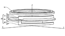
図6及び図7は本実施形態におけるアンテナ30の構成を説明するための模式図である。図6に示すように、本実施形態のアンテナ30は、第1の放射素子としての円弧状の第1リボン31と、第2の放射素子としての円弧状の第2リボン35と、グラウンド板としての回路基板26とを備えている。
第1リボン31は、円弧状のリボン部32と、直線状の給電部33と、直線状のアンテナ電極34とを備えている。
第1リボン31のリボン部32、給電部33、及びアンテナ電極34は、銅線、アルミニウム、銀等のパイプ等を用いて容易に構成できる。抵抗の少ない金属を用いることが好ましい。銅線やアルミニウム等の薄板を用いてもよい。適当な形状の基台に導電性の箔の貼付やエッチング、印刷等によって形成してもよい。ケース本体11の内壁にメッキを施すことによって形成してもよい。また、プラスチック等のコア材にリボンを這わせるような構造も可能である。
リボン部32の一端には、給電部33及びアンテナ電極34が接続され、リボン部32の他の一端は開放されている。給電部33とアンテナ電極34とは回路基板26に接続されている。給電部33は回路基板26の信号パターンに接続され、アンテナ電極34は回路基板26のGNDパターンに接続されている。
C: Detailed Configuration of Antenna Next, the configuration of the
6 and 7 are schematic diagrams for explaining the configuration of the
The
The
The feeding
第1リボン31は、図4に示すように、外装ケース2の内部空間において、表示部20の側方の位置であって、腕時計における6時側に配置されている。外装ケース2を構成するケース本体11の内側には、例えば図示しない溝が形成されており、第1リボン31は当該溝内に収容され保持される。なお、第1リボン31を保持する方法は、溝を用いる方法だけでなく、例えばケース本体11の内側に第1リボン31を案内する凸部を複数個所に設け、これらの凸部によって保持する方法を用いてもよい。
As shown in FIG. 4, the
なお、ベゼル16は、ステンレススチール、チタン、アルミニウム、銅、銀などの金属製であり、切欠きのないリング状(O字形状)に形成されている。ベゼル16としては、金属製のベゼル以外にも、樹脂等にメッキを施すことにより形成したベゼルも使用可能である。
The
本実施形態のアンテナ30における第1リボン31は、長さが1λよりも十分に短いダイポールアンテナを折り曲げて、円弧状のループ素子(磁流素子)としてのリボン部32と、直線素子(電流素子)としてのアンテナ電極34とを形成し、給電部33によりリボン部32とアンテナ電極34に給電を行った場合と同様の構成となっている。
第1リボン31は、図2に示すように、平面視においてベゼル16と重なる位置に配置されており、上下方向(図2の平面方向に垂直な方向、表示部20の表示方向)においてベゼル16よりも下方に配置され、無給電素子としてのベゼル16と所定の間隔を有している。
上述のような構成により、ベゼル16を第1リボン31に電磁界結合させることが可能になる。本実施形態では、後述するように、電磁界結合させたベゼル16を直線素子(電流素子)の延長として利用している。
第1リボン31には、給電点を移動させるための給電部33が接続されている。アンテナ電極34は回路基板26のGNDパターンに接続され、給電部33は回路基板26の信号パターンに接続されている。当該構成においては、アンテナ電極34とベゼル16が電流ベクトルを発する電流素子として動作し、リボン部32が磁流ベクトルを発する磁流素子として動作する。つまり、回路基板26はGND板として機能し、回路基板26は前記上下方向において第1リボン31の下方に配置されている。
The
As shown in FIG. 2, the
With the configuration as described above, the
A
本実施形態では、腕時計としての電子機器1は、表示部の視認性および時計の携帯性を満足するために、腕時計を平面視したときの外装ケースの外形形状が、直径が約20mm以上50mm以内で以下に構成するのか好ましい。ベゼル16は、第1リボン31とは異なり切欠きが設けられておらず、閉じたO字形状のリングである。本実施形態では、一例として、直径30mmのベゼル16が用いられている。したがって、ベゼル16の周長は約90mmとなっている。
但し、ベゼル16は、切欠きのないO字形状のリングなので、ベゼル16に流れる電流には対称性があり、ループ素子としては機能しない。つまり、仮にベゼル16の1点に給電したとしても、電流は、当該給電点から双方向に流れることになる。したがって、ベゼル16は、等価的に一本の直線素子として考えられ、等価電気長は、ベゼル16の周長ではなく、直径に近い長さとなる。
本実施形態の電子機器1は、上述したように約1.5GHz、1波長(1λ)が約200mmのGPS電波を受信する。したがって、ベゼル16の等価電気長は、1λよりも十分に短くなっている。本実施形態のアンテナ30においては、ベゼル16の等価電気長と、第1リボン31の等価電気長と、アンテナ電極34の等価電気長とを加えた等価電気長が、1/4λとなるように設定されている。
In the present embodiment, in the
However, since the
As described above, the
第2リボン35は、円弧状のリボン部36と、直線状のアンテナ電極37とを備えている。
第2リボン35のリボン部36及びアンテナ電極37は、第1リボン31と同様に、銅線、アルミニウム、銀等のパイプを用いて容易に構成できる。抵抗の少ない金属を用いることが好ましい。銅線やアルミニウム等の薄板を用いてもよい。適当な形状の基台に導電性の箔の貼付やエッチング、印刷等によって形成してもよい。ケース本体11の内壁にメッキを施すことによって形成してもよい。また、プラスチック等のコア材にリボンを這わせるような構造も可能である。
リボン部36の一端には、アンテナ電極37が接続され、リボン部36の他の一端は開放されている。アンテナ電極37は回路基板26のGNDパターンに接続されている。
The
Like the
The
第2リボン35は、図6に示すように、回路基板26に対して第1リボン31と対称の位置であって、第1リボン31の電気影像の位置に設けられている。つまり、第2リボン35は、第1リボン31による回路基板26における電流の方向に沿った配置となっている。なお、第2リボン35の配置は、回路基板26における電流の方向に沿った配置に限定されるものではなくも、回路基板26の外側に理論上流れる電流の方向に沿った配置でもよい。また、第2リボン35は、電流分布のうち電流が強い部分の方向に概ね沿っていれば良い。
第2リボン35のアンテナ電極37は回路基板26のGNDパターンに接続されており、第1リボン31のアンテナ電極34の接地点を電気的に共有する位置に接続されている。第1リボン31には給電部33が設けられており給電が行われるが、第2リボン35には給電を行う必要がないため、給電部は設けられていない。したがって、L字型のリボンとなる。
なお、外装ケース2を構成するケース本体11の内側には、例えば図示しない溝が形成されており、第2リボン35は当該溝内に収容され保持される。第2リボン35を保持する方法は、溝を用いる方法だけでなく、例えばケース本体11の内側に第2リボン35を案内する凸部を複数個所に設け、これらの凸部によって保持する方法を用いてもよい。
As shown in FIG. 6, the
The
In addition, for example, a groove (not shown) is formed inside the
GND板としての回路基板26が十分に大きい場合には、回路基板26に対して第1リボン31と対称の位置には、影像アンテナが形成されることになる。つまり、第2リボン35は、アンテナ電極37が第1リボン31のアンテナ電極34の接地点を電気的に共有する位置に接続されており、回路基板26に対して第1リボン31と対称の位置に設けられているため、実際に存在する影像アンテナとして機能することになる。
また、本実施形態においては、ベゼル16の等価電気長と第1リボン31の等価電気長を加えた等価電気長が1/4λとなるように設定されており、第2リボン35の等価電気長も1/4λとなるように設定されている。したがって、本実施形態のアンテナ30は、グランドプレーンアンテナのように、等価電気長が1/2λのアンテナとして動作することになる。
以上のように、本実施形態においては、表示部20とアンテナ30が外装ケース2の内部にあり、外装ケース2は裏蓋12を含む。そして、無給電素子としてのベゼル16の位置は、表示部20に対して裏蓋12とは反対側の位置となっている。さらに、第1の放射素子としての第1リボン31の位置は、ベゼル16と裏蓋12との間の位置となっている。 なお、ベゼル16の代わりとして、無給電素子として機能する金属を含む部材を、表示部20上に設けるようにしてもよい。無給電素子として機能する金属を含む部材を表示部20上に設ける場合も、無給電素子の位置は、表示部20に対して裏蓋12とは反対側の位置である。さらに、第1の放射素子としての第1リボン31の位置は、無給電素子と裏蓋12との間の位置となっている。
When the
In addition, in the present embodiment, the equivalent electrical length of the
As described above, in the present embodiment, the
次に、本実施形態のアンテナ30の指向性について説明する。まず、第1リボン31のみを用いた場合の指向性について説明する。なお、アンテナの送信と受信は同じ現象の+−符号を変えただけなので、ここでは説明の簡略化のため送信で説明する。図18Bに示すように第1リボン31に対してGND板としての回路基板26が十分に大きい場合には、アンテナとして第1リボン31のみを用いた電子機器1を腕に装着したとしても、指向性は図18Aに示すように理想的な水平なドーナッツ型に近い指向性を示す。つまり、腕方向の指向性が小さくなり、腕によって吸収される電力は少なく、感度劣化は生じない。なお、図18Bの例では、GND板として直径90mmの回路基板26を想定している。また、図18Bに示す直方体50は腕を疑似的に示している。
Next, the directivity of the
一方、図19Bに示すように、GND板が例えば腕時計に用いられる回路基板26のように直径40mm程度の場合には、アンテナとして第1リボン31のみを用いて電子機器1を腕に装着すると、図19Aに示すように指向性が腕の方向を向いてしまい、腕の方向に向いた電力が腕に吸収されアンテナの放射効率を劣化させる。
On the other hand, as shown in FIG. 19B, when the GND plate has a diameter of about 40 mm like the
GND板が十分に大きい場合には、図20に矢印Cで示す方向、すなわち、腕に水平な方向に第1リボン31を流れる電流は、矢印C’で示す方向に回路基板26を流れる電流でキャンセルされる。したがって、矢印Bで示す上下方向に流れる電流のみが存在し、回路基板26に対して第1リボン31と対称な影像アンテナが現れる。したがって、アンテナの指向性は、図18Aに示すように、理想的な水平なドーナッツ型に近くなる。
しかし、GND板が十分には大きくない場合には、図21に矢印D及び矢印Eで示すように第1リボン31の片側(回路基板26の内側)に電流分布が偏るため、GND板が十分に大きい場合のように腕に水平な電流がキャンセルされなくなる。したがって、第1リボン31のみの場合には影像アンテナの形が崩れると考えられ、グランドプレーンアンテナではなく、腕に水平な方向に置いたダイポールアンテナの動作に近づいてしまう。したがって、図19Aに示すようにアンテナの指向性が腕の方向を向いてしまい、腕の方向に向いた電力が腕に吸収され感度劣化が生じることになる。
When the GND plate is sufficiently large, the current flowing through the
However, when the GND plate is not sufficiently large, the current distribution is biased to one side of the first ribbon 31 (inside the circuit board 26) as shown by arrows D and E in FIG. The horizontal current in the arm is not canceled as in the case of a large size. Therefore, when only the
そこで、本実施形態では、図6に示すように、影像アンテナに相当する位置に第2リボン35を実際に設け、GND板が小さい場合でも、GND板が十分に大きい場合の動作モードに近づけている。影像アンテナに相当する位置に第2リボン35が設けられていることにより、図8に示すように指向性は水平に近づくように傾き、腕によって吸収される電力が減少し、感度劣化を防ぐことができる。
Therefore, in the present embodiment, as shown in FIG. 6, the
次に、本実施形態のアンテナ30の大きさについて説明する。約1.5GHzのGPS電波は、1λが約200mmであり、アンテナ30の等価的電気長である1/4λは約50mmとなる。但し、λは自由空間波長であり、実際には周囲の部材の影響等により、所定内の範囲に設定されている。例えば、本実施形態では、一例として、0.8×(1/4λ)〜1.3×(1/4λ)の範囲、つまり、40mm〜65mmの範囲に設定される。
第1リボン31は、図9に示すように、一例として、リボン部32の幅が2mm、リボン部32の長さが35.5mm、アンテナ電極34の長さが7mmのものを使用している。当該長さは、1/4λを約50mmとした場合に、1/4λ×0.85の長さとなる。厚さは100μmとなっている。
ベゼル16の等価電気長は、原則的にベゼル16の直径を通る所定の線に対称に電流が流れるため、ベゼル16の円周の約半分の長さである45mmである。しかし、ベゼル16は、腕時計の平面視で第1リボン31と重なる位置に配置されている。当該配置により、腕時計の平面視で第1リボン31と重なるベゼル16部分(以下、重複部と称する)はアンテナ30の等価電気長として第1リボン31とベゼル16とで重複して機能する。本実施形態では、重複部の長さは約35mmであるので、ベゼル16の実質的な等価電気長は、約10mmとなっている。
したがって、本実施形態では、ベゼル16の等価電気長と第1リボン31のリボン部32の長さとアンテナ電極34の長さとを足した長さが約52.5mmで1.15×(1/4λ)となるように設定されている。
Next, the size of the
As shown in FIG. 9, the
The equivalent electrical length of the
Therefore, in this embodiment, the equivalent electrical length of the
また、第2リボン35は、図9に示すように、一例として、リボン部36の幅2mm、リボン部36の長さが35.2mm、アンテナ電極37の長さが3mmのものを使用している。厚さは100μmとなっている。当該長さは、1/4λを約50mmとした場合に、1/4λ×0.76の長さとなる。
As the
回路基板26とリボン部32,36との距離、すなわち、アンテナ電極34,37の長さと、放射効率との間には、図10に示す関係がある。第1リボン31及び第2リボン35の全長は決まった長さ(波長の約1/4)なので、第1リボン31及び第2リボン35の水平部分であるリボン部32,36が短いほど垂直部分であるアンテナ電極34,37は長くなる。そして水平部分であるリボン部32,36が無くなったときがアンテナ電極34,37の長さ、つまり、回路基板26とリボン部32,36との距離の上限値となる。そして、図10に示すように、放射効率は当該上限値まで単調増加する。
第1リボン31及び第2リボン35の垂直部分であるアンテナ電極34,37による電界と、水平部分であるリボン部32,36による電界が概略等しいときに、原理上円偏波が最も強くなる。したがって、垂直部分であるアンテナ電極34,37の長さと水平部分であるリボン部32,36の長さが等しいときが最も放射効率が高くなる。例えば、1/4λを約50mmとした時に、リボン部32,36の長さが25mmで、アンテナ電極34,37が25mmの時に最も放射効率が高くなる。
しかしながら、例えば腕時計型の電子機器の場合には、電子機器の高さは10mm程度なので、アンテナ電極34,37が25mmに設定することはできない。そこで、本実施形態のように、アンテナ電極34,37の長さ、つまり、回路基板26とリボン部32,36との距離として、3〜7mm程度を採用している。
なお、これらの長さは、モメント法などのシミュレーションによって決めることができる。
The distance between the
In principle, the circularly polarized wave becomes the strongest when the electric fields due to the
However, for example, in the case of a wristwatch type electronic device, the height of the electronic device is about 10 mm, and therefore the
Note that these lengths can be determined by a simulation such as the Moment method.
また、第2リボン35のリボン部36の長さと放射効率と指向性との間には、図11に示すような関係がある。図11に示すように、第2リボン35のリボン部36の長さを変えると指向性が変化し、腕に電子機器1を装着した場合には、リボン部36の長さが36mmの場合に最も放射効率が高くなる。また、指向性は最も水平方向に近づき、腕方向の指向性が最少となる。つまり、腕方向の指向性が最少となるため、腕により吸収される電力が最少となり、最も放射効率が高くなる。
本実施形態では、上述したように、第2リボン35のリボン部36の長さ35.2mm程度に設定しているため、第1リボン31だけでは30%であった放射効率を、50%まで大幅に改善することができた。
Further, the length of the
In the present embodiment, as described above, since the length of the
以上のように本実施形態によれば、逆F型のアンテナとしての第1リボン31に対して、影像のアンテナである第2リボン35を実際に設けた構成としたので、GND板としての回路基板26を十分に大きくすることができない場合でも、腕方向の指向性を減少させて放射効率を向上させ、感度低下を防ぐことができる。
As described above, according to the present embodiment, the
なお、本実施形態においては、図2に示すように、第1リボン31及び第2リボン35の中心位置が5時位置付近となるように配置されているが、本発明は当該構成に限定されるものではない。例えば、第1リボン31及び第2リボン35の中心位置が6時位置付近となるように配置してもよい。
In addition, in the present embodiment, as shown in FIG. 2, the
<第2実施形態>
次に、本発明の第2実施形態について図12を参照しつつ説明する。以下の説明において、第1実施形態と共通の構成については、同一の符号を使用し、重複する説明は省略する。第1実施形態においては、第2リボン35を第1リボン31の影像の位置、つまり、回路基板26に対して第1リボン31と対称な位置に設けた構成について説明した。しかしながら、本実施形態においては、第2リボン35を第1リボン31と同じ側に設ける。
<Second Embodiment>
Next, a second embodiment of the present invention will be described with reference to FIG. In the following description, the same components as those in the first embodiment will be designated by the same reference numerals, and overlapping description will be omitted. In the first embodiment, the configuration in which the
図12に点線で示すように回路基板26が十分に大きい場合には、電流は矢印で示すように回路基板26上に分布する。しかし、図12に実線で示すように回路基板26が小さくなると、矢印で示した電流の一部は実線で示した回路基板26の内側に分布するが、矢印で示した電流の他の一部は実線で示した回路基板26の外側に位置することになる。つまり、回路基板26の外側に位置するように示した前記他の一部の電流は、実線で示した回路基板26上を流れる電流としては存在しないことになる。
そこで、本実施形態においては、回路基板26を十分に大きくできない場合に欠落することになる電流分布を、第1リボン31と同じ面側に設けた第2リボン35により補っている。
第2リボン35の長さは、第1実施形態と同様に1/4λ付近に設定し、アンテナの周波数と共振させる。したがって、有限長の第2リボン35に最大限電流を流すことができる。本実施形態においては、上述したように回路基板26の外側に位置することになる電流の分布を、第2リボン35に流れる電流によって再現している。
したがって、回路基板26が十分に大きい場合と同様に、腕方向の指向性を減少させることができ、腕で消費される電力を減少させて感度低下を防止することができる。
When the
Therefore, in the present embodiment, the current distribution that would otherwise be missing if the
The length of the
Therefore, as in the case where the
また、第1実施形態においては、第2リボン35の位置は、平面視において第1リボン31とほぼ同じ位置に設けていたが、本実施形態のように、第2リボン35の位置は、平面視において第1リボン31の位置と一致していなくてもよい。これは、回路基板26が小さいために、回路基板26の外側に位置することになる電流分布を第2リボン35によって再現できればよいからである。
さらに、第2リボン35の位置は、平面視において第1リボン31よりも内側に位置していてもよい。第1リボン31よりも内側に位置した場合には、回路基板26の位置することになる電流分布を回路基板26の内側に位置に発生させることになり、同様の効果が得られる。
また、図12におけるZ方向上の位置が、第1リボン31よりも高い位置であってもよい。第1リボン31よりも高い位置場合には、回路基板26の位置することになる電流分布を回路基板26の上方の位置に発生させることになり、同様の効果が得られる。
Further, in the first embodiment, the position of the
Furthermore, the position of the
Further, the position in the Z direction in FIG. 12 may be higher than the
なお、本実施形態においても、第1実施形態と同様に、第2リボン35を回路基板26に対して第1リボン31と対称の位置に設けるようにしてもよい。第1リボン31と対称の位置に設ける場合でも、第2リボン35は平面視において回路基板26よりも外側の位置にあってもよく、第1リボン31よりも内側に位置していてもよい。
いずれの場合も、第2の放射素子としての第2リボン35を、理論上流れる電流の密度の高い場所に配置することが好ましい。本実施形態においては、第1放射素子としての第1リボン31による回路基板26上の電流の方向に沿って配置している。なお、第2リボン35の配置は、回路基板26における電流の方向に沿った配置に限定されるものではなくも、回路基板26の外側に理論上流れる電流の方向に沿った配置でもよい。また、第2リボン35は、電流分布のうち電流が強い部分の方向に概ね沿っていれば良い。 第1リボン31と第2リボン35の接地点は、第1の実施形態と同様に、電気的に共有される位置に設けることが重要である。例えば、本実施形態のように、回路基板26の縁部付近に接地点を設けることにより、それぞれの接地点が距離的に近くなり、電気的に共有されることになる。
In the present embodiment as well, as in the first embodiment, the
In either case, it is preferable to dispose the
<第3実施形態>
次に、本発明の第3実施形態について図13を参照しつつ説明する。以下の説明において、第1実施形態及び第2実施形態と共通の構成については、同一の符号を使用し、重複する説明は省略する。上述の実施形態においては、金属製のベゼル16を用いる構成について説明したが、本実施形態は金属製のベゼル16を用いない構成となっている。
金属製のベゼル16を用いる場合には、厳密にはベゼル16の影像として回路基板26に対して対称なエレメントが必要になる。したがって、図13に示すように、金属製のベゼルを用いない構成の方が本発明の効果を顕著に発揮することができる。例えば、金属製のベゼル16と第2リボン35を用いた場合には、放射効率は−3.3dB(46%)であるのに対し、金属製のベゼル16を用いずに第2リボン35を用いた場合には、放射効率は−3.1dB(48%)であった。なお、金属製のベゼル16を用いて第2リボン35を用いない場合には、放射効率は−4.5dB(35%)であるのに対し、金属製のベゼル16も第2リボン35も用いない場合には、放射効率は−4.8dB(33%)であった。
図13に示す例は、第1実施形態の図6に対応する図であり、金属製のベゼル16が備えられていない点が第1実施形態と異なっている。
金属製のベゼルを用いない場合とは、プラスチック製のベゼルを用いる場合、あるいは、ベゼルそのものを用いない構成が含まれる。
本実施形態によれば、逆F型のアンテナとしての第1リボン31に対して、影像のアンテナである第2リボン35を実際に設けた構成としたので、GND板としての回路基板26を十分に大きくすることができない場合でも、腕方向の指向性を減少させて放射効率を向上させ、感度低下を防ぐことができる。
<Third Embodiment>
Next, a third embodiment of the present invention will be described with reference to FIG. In the following description, the same components as those in the first and second embodiments are designated by the same reference numerals, and the duplicated description will be omitted. Although the configuration using the
When the
The example shown in FIG. 13 is a diagram corresponding to FIG. 6 of the first embodiment, and differs from the first embodiment in that the
The case where the metal bezel is not used includes the case where the plastic bezel is used or the configuration where the bezel itself is not used.
According to the present embodiment, since the
<第4実施形態>
次に、本発明の第4実施形態について図14を参照しつつ説明する。以下の説明において、第1実施形態ないし第3実施形態と共通の構成については、同一の符号を使用し、重複する説明は省略する。上述の実施形態においては、板状のリボンを用いる構成について説明したが、本実施形態では、針金状のリボンを用いる構成である。
上述した実施形態においては、製造状の利便性を重視して、薄い板状金属を用いて第1リボン31と第2リボン35を形成していた。これらのリボンは大きな金属版をプレス等で当該形に切り抜くことにより低コストで寸法精度良く製造できる。また面積をとることで表皮効果によって流れる電流の面積を広くし、これによってリボンの単位長さあたりの抵抗を小さくし放射効率を0.1〜0.3dB程度改善することもできる。
<Fourth Embodiment>
Next, a fourth embodiment of the present invention will be described with reference to FIG. In the following description, the same components as those in the first to third embodiments are designated by the same reference numerals, and the duplicate description will be omitted. In the above-described embodiment, the configuration using the plate-shaped ribbon has been described, but in the present embodiment, the wire-shaped ribbon is used.
In the embodiment described above, the
一方、筐体の形状によってはリボンの幅を確保できない場合もある。当該場合には、図14に示すように板状ではなく断面が正方形や円やなどの針金を用いて第1リボン31と第2リボン35を形成することも可能である。図14に示す構成の場合には、上記表皮効果により電流が流れる面積は狭くなるため、若干感度劣化を起こすが、十分実用に供することができる。リボンを針金で形成する場合には、材質としては抵抗の少ない金属がよい。例えば、銅、アルミ、銀等が挙げられる。
なお、本実施形態においても、第3実施形態のように金属製のベゼル16を用いない構成としてもよい。
On the other hand, the width of the ribbon may not be secured depending on the shape of the housing. In this case, as shown in FIG. 14, it is possible to form the
Note that, also in the present embodiment, a configuration in which the
<第5実施形態>
次に、本発明の第5実施形態について図15を参照しつつ説明する。以下の説明において、第1実施形態ないし第4実施形態と共通の構成については、同一の符号を使用し、重複する説明は省略する。上述の実施形態においては、円弧状の第2リボン35を用いる構成について説明したが、本実施形態では、一部が屈曲した形状の第2リボン35を用いる。
図15は本実施形態におけるアンテナ30の概略構成を示す斜視図である。図15に示すように、本実施形態の第2の放射素子としての第2リボン35は、一部に屈曲部36aを備えている。第2リボン35の一部に屈曲部36aが形成されていても、接地点に接続された第2リボン35のアンテナ電極37の端部から、第2リボン35の開放された端部36bまでの方向が、第1リボン31による回路基板26上の電流の方向に沿って配置されていれば、上述の実施形態と同様の効果を奏することができる。なお、第2リボン35の配置は、回路基板26における電流の方向に沿った配置に限定されるものではなくも、回路基板26の外側に理論上流れる電流の方向に沿った配置でもよい。また、第2リボン35は、電流分布のうち電流が強い部分の方向に概ね沿っていれば良い。本実施形態においても、第2リボン35は、理論上流れる電流の密度の高い場所に配置することが好ましい。 本実施形態によれば、第2リボン35の一部に屈曲部36aを設けたので、円弧状の第2リボン35を配置することが困難な場合であっても本発明のアンテナの構成を実現することができる。
<Fifth Embodiment>
Next, a fifth embodiment of the present invention will be described with reference to FIG. In the following description, the same components as those in the first to fourth embodiments are designated by the same reference numerals, and the duplicate description will be omitted. Although the configuration using the arc-shaped
FIG. 15 is a perspective view showing a schematic configuration of the
<第6実施形態>
次に、本発明の第6実施形態について図16を参照しつつ説明する。以下の説明において、第1実施形態ないし第5実施形態と共通の構成については、同一の符号を使用し、重複する説明は省略する。第1実施形態においては、電子機器の一例として、デジタル式のランニングウォッチに本発明を適用した。本実施形態は、電子機器の一例として、アナログ式のGPSウォッチに本発明を適用する。
<Sixth Embodiment>
Next, a sixth embodiment of the present invention will be described with reference to FIG. In the following description, the same components as those in the first to fifth embodiments are designated by the same reference numerals, and the duplicate description will be omitted. In the first embodiment, the present invention is applied to a digital running watch as an example of an electronic device. The present embodiment applies the present invention to an analog GPS watch as an example of an electronic device.
図16に示す本実施形態の電子機器1aは、ソーラーパネルで発電した電力により駆動され、GPS信号を受信することにより時刻修正を行うソーラー駆動の電波修正時計である。電子機器1aは、外装ケース80を備えている。外装ケース80は、金属で形成された円筒状のケースである。外装ケース80には、金属で形成されたベゼル16が嵌合されて構成されている。
The
ベゼル16の内周側に、プラスチックで形成されたリング状のダイヤルリング83を介して、円盤状の文字板81が時刻表示部分として配置され、文字板81上には、時刻や日付等を表示する指針17が配置されている。指針17は、時針17aと、分針17bと、秒針17cとから構成される。文字板81には日付視認窓18aが開口形成されており、日車18に表示された日付が日付視認窓18aから視認可能となっている。
外装ケース80の表面側の開口は、ベゼル16を介してカバーガラス84で塞がれており、カバーガラス84を通じて、内部の文字板81、指針17(時針17a、分針17b、秒針17c)が視認可能となっている。
A disc-shaped
The opening on the surface side of the
電子機器1aは、竜頭86を手動操作することにより、手動の時刻修正が可能であり、また、操作ボタン87を手動操作することにより、通常時刻表示モードと時差修正モードとを切り替えることが可能に構成されている。なお、本実施形態の電子機器1aは、毎日、自動的にGPS信号を受信して、時刻を修正する時刻修正機能を有している。操作ボタン87を手動操作することにより、GPS信号を強制的に受信させることも可能となっている。
The
本実施形態においても、アンテナ30は、円弧状の第1リボン31と、回路基板26(図16には図示せず)と、円弧状の第2リボン35(図16には図示せず)を備えている。第1リボン31は、円弧状のリボン部32と、直線状の給電部33と、直線状のアンテナ電極34とを備えている。また、図示を省略するが、第2リボン35は、円弧状のリボン部36と、直線状のアンテナ電極37とを備えている。他のアンテナ30に関する構成についても第1実施形態と同様である。
Also in this embodiment, the
本実施形態の第1リボン31及び第2リボン35は、接地点から延びる方向が、第1実施形態と異なり、平面視で左周りとなっている。第1リボン31及び第2リボン35の延びる方向が左周りであっても、周辺にある部品の影響で、第1実施形態と同様に、腕に装着した際の感度低下を防止することができる。
Unlike the first embodiment, the
以上のように、本発明のアンテナ30は、指針式のGPSウォッチにも適用することができる。また、第1リボン31及び第2リボン35の延びる方向は左周りとすることもできる。
なお、上述した第2実施形態から第5実施形態の構成を指針式のGPSウォッチに適用してもよい。
As described above, the
The configurations of the second to fifth embodiments described above may be applied to a pointer-type GPS watch.
<変形例>
本発明は、上述した実施形態に限定されるものではなく、例えば次に述べるような各種の変形が可能である。また、次に述べる変形の態様は、任意に選択された一または複数を、適宜に組み合わせることもできる。
<Modification>
The present invention is not limited to the above-described embodiment, and various modifications such as those described below are possible. In addition, one or more arbitrarily selected aspects of the modifications described below can be appropriately combined.
(変形例1)
上述した各実施形態では、第1リボン31及び第2リボン35として、円弧状のリボンを採用した例について説明した。しかし、本発明は当該例に限定される訳ではなく、例えば、四角形状であってもよい。
図17は、第1リボン31a及び第2リボン35aとして、四角形状(口の字形状)のリボンを採用した場合のアンテナ30aの構成を説明するための模式図である。表示部の表示面に垂直な方向から平面視したとき、外装ケースが円筒形ではなく、矩形の筒形であるウォッチ等の電子機器の場合には、外装ケースに合わせて第1リボン31a及び第2リボン35aも四角形状に形成することができる。
第1リボン31aは、リボン部32aを備えており、リボン部32aの一端に矩形のアンテナ電極34aと給電部33aとを接続する。同様に、第2リボン35aは、リボン部36bを備えており、リボン部36bの一端に矩形のアンテナ電極37aを接続する。第2リボン35aは、回路基板26aに対して、対称の位置に設けられている。第1リボン31aと第2リボン35aの接地点は、電気的に共有される位置に設定されている。
(Modification 1)
In each of the above-described embodiments, an example in which arc-shaped ribbons are used as the
FIG. 17 is a schematic diagram for explaining the configuration of the
The
第1リボン31aと第2リボン35aは、以上のように四角形状のリボンであってもよく、L字形状であってもよい。
なお、本変形例においてベゼルを用いる場合には、ベゼルも四角枠形状にすればよい。また、いずれの場合も、リボンの一部に屈曲部が形成されていてもよい。
The
When the bezel is used in this modification, the bezel may also have a rectangular frame shape. In any case, a bent portion may be formed on a part of the ribbon.
(変形例2)
上述した各実施形態及び各変形例においては、本発明のアンテナにおいて1.5GHzのGPS電波を受信する場合について説明したが、本発明は当該構成に限定されるものではない。本発明のアンテナは、例えば、周波数が100MHzから30GHzの電波を受信に好適である。
本発明を腕時計のサイズの電子機器に適用する場合には、GPSの1.5GHz、あるいは無線LANの2.4GHz付近が最適である。また、本発明を携帯電話のサイズの電子機器に適用する場合には、携帯電話で使っている700MHzあるいは900MHzが最適になる。
利用可能な測位用衛星の信号としては、GPSの他に、GLONASS(GLObal NAvigation Satellite System)、GALILEO、BeiDou(BeiDou Navigation Satellite System)、WAAS(Wide Area Augmentation System)、QZSS(Quasi Zenith Satellite System)等が挙げられる。
(Modification 2)
In each of the embodiments and the modifications described above, the case where the antenna of the present invention receives the GPS radio wave of 1.5 GHz has been described, but the present invention is not limited to the configuration. The antenna of the present invention is suitable for receiving radio waves having a frequency of 100 MHz to 30 GHz, for example.
When the present invention is applied to a wristwatch-sized electronic device, GPS of 1.5 GHz or wireless LAN of 2.4 GHz is optimal. When the present invention is applied to an electronic device of the size of a mobile phone, 700 MHz or 900 MHz used in the mobile phone is optimal.
Examples of usable positioning satellite signals include GLONASS (GLObal NAvigation Satellite System), GALILEO, BeiDou (BeiDou Navigation Satellite System), WAAS (Wide Area Augmentation System), QZSS (Quasi Zenith Satellite System), etc. in addition to GPS. Is mentioned.
また、Bluetooth(登録商標)、あるいは、Wi−Fi(登録商標)等の規格に対応した電波を受信するようにしてもよい。 Further, it may be configured to receive a radio wave corresponding to a standard such as Bluetooth (registered trademark) or Wi-Fi (registered trademark).
(変形例3)
上述した各実施形態及び各変形例においては、第1の放射素子としての第1リボンと、第2の放射素子としての第2リボンとの等価電気長がそれぞれ1/4波長の場合について説明したが、本発明は当該構成に限定されるものではない。例えば、前記等価電気長は、1/4波長の整数倍であればよい。
(Modification 3)
In each of the above-described embodiments and modified examples, the case where the equivalent electrical lengths of the first ribbon as the first radiating element and the second ribbon as the second radiating element are each 1/4 wavelength has been described. However, the present invention is not limited to this configuration. For example, the equivalent electrical length may be an integral multiple of 1/4 wavelength.
(変形例4)
上述した各実施形態及び各変形例においては、本発明の電子機器の例として、ランニングウォッチ、及びGPSウォッチを挙げたが、本発明はこれらに限定されるものではない。本発明は、アンテナにより電波を受信して情報を表示する種々の電気機器に適用可能である。例えば、腕時計型の心拍計、イヤホン型のGPS機器、スマートフォン等の電子機器(電子端末)、ヘッドマウントディスプレイ等のウェアラブルな電子機器にも適用可能である。
(Modification 4)
Although the running watch and the GPS watch are given as examples of the electronic device of the invention in the above-described embodiments and modifications, the invention is not limited thereto. INDUSTRIAL APPLICABILITY The present invention can be applied to various electric devices that receive radio waves by an antenna and display information. For example, the present invention can be applied to wristwatch type heart rate monitors, earphone type GPS devices, electronic devices (electronic terminals) such as smartphones, and wearable electronic devices such as head mounted displays.
1,1a……電子機器、2……外装ケース、3……バンド、11……ケース本体、12……裏蓋、13……ガラス、14……支持リング、15……パッキン、16,16a……ベゼル、20……表示部、21……液晶パネル、22……パネル枠、26……回路基板、30,30a……アンテナ、31,31a……第1リボン、32,32a……リボン部、33,33a……給電部、34,34a……アンテナ電極、35,35a……第2リボン、36……リボン部、36a……屈曲部、36b……リボン部、37,37a……アンテナ電極、80……外装ケース、81……文字板、83……ダイヤルリング、84……カバーガラス。
1, 1a...Electronic device, 2...Exterior case, 3...Band, 11...Case body, 12...Back cover, 13...Glass, 14...Support ring, 15...Packing, 16,16a ...Bezel, 20...display section, 21...liquid crystal panel, 22...panel frame, 26...circuit board, 30,30a...antenna, 31,31a...first ribbon, 32,32a...ribbon Part, 33, 33a... Feed part, 34, 34a... Antenna electrode, 35, 35a... Second ribbon, 36... Ribbon part, 36a... Bent part, 36b... Ribbon part, 37, 37a. Antenna electrode, 80... Exterior case, 81... Dial, 83... Dial ring, 84... Cover glass.
Claims (9)
前記第1の放射素子が接地する接地点を有するグラウンド板と、
前記接地点を電気的に共有する位置において前記グラウンド板に接地された第2の放射素子と、を含み、
前記第1の放射素子は、前記グラウンド板に垂直な方向から見た平面視において、前記グラウンド板と重なり、
前記第2の放射素子は、前記グラウンド板を挟んで前記第1の放射素子の反対側にあり、前記平面視において、前記グラウンド板と重なる、
ことを特徴とするアンテナ。 A first radiating element,
A ground plate having a ground point at which the first radiating element is grounded;
A second radiating element grounded to the ground plate at a position electrically sharing the ground point,
The first radiating element is overlapped with the ground plate in a plan view seen from a direction perpendicular to the ground plate,
Said second radiating element, Ri opposite near the across the grayed round plate first radiating element, in the plan view, overlaps with the ground plate,
An antenna characterized by that.
ことを特徴とする請求項1に記載のアンテナ。 The first radiating element and the second radiating element are arc-shaped in a plan view seen from a direction perpendicular to the ground plate,
The antenna according to claim 1, wherein:
ことを特徴とする請求項1または請求項2に記載のアンテナ。 The second radiating element includes a bent portion,
The antenna according to claim 1 or 2, characterized in that.
ことを特徴とする請求項1ないし請求項3のいずれか1項に記載のアンテナ。 The equivalent electrical length of the first radiating element and the second radiating element is 1/4 wavelength,
The antenna according to any one of claims 1 to 3, wherein:
前記第1の放射素子が接地する接地点を有するグラウンド板と、
前記接地点を電気的に共有する位置において前記グラウンド板に接地された第2の放射素子と、を含むアンテナを有し、
前記第1の放射素子は、前記グラウンド板に垂直な方向から見た平面視において、前記グラウンド板と重なり、
前記第2の放射素子は、前記グラウンド板を挟んで前記第1の放射素子の反対側にあり、前記平面視において、前記グラウンド板と重なる、
ことを特徴とする電子機器。 A first radiating element,
A ground plate having a ground point at which the first radiating element is grounded;
A second radiating element that is grounded to the ground plate at a position that electrically shares the ground point;
The first radiating element is overlapped with the ground plate in a plan view seen from a direction perpendicular to the ground plate,
It said second radiating element, across the grayed round plate located opposite said first radiating element, in the plan view, overlaps with the ground plate,
An electronic device characterized in that
前記表示部および前記アンテナを収容し、裏蓋を含むケースと、
金属を含む無給電素子と、を含み、
前記無給電素子の位置は、前記表示部に対して前記裏蓋とは反対側であり、
前記第1の放射素子の位置は、前記無給電素子と前記裏蓋との間である、
ことを特徴とする請求項5に記載の電子機器。 Display part,
A case that houses the display unit and the antenna and includes a back cover;
And a parasitic element containing metal,
The position of the parasitic element is opposite to the back cover with respect to the display unit,
The position of the first radiating element is between the parasitic element and the back cover,
The electronic device according to claim 5, wherein:
ことを特徴とする請求項5または請求項6に記載の電子機器。 The ground plate is a circuit board of the electronic device,
7. The electronic device according to claim 5 or 6, characterized in that.
前記アンテナは、
第1の放射素子と、
前記第1の放射素子が接地する接地点を有するグラウンド板と、
前記接地点を電気的に共有する位置において前記グラウンド板に接地された第2の放射素子と、
を含み、
前記第2の放射素子は、前記グラウンド板を挟んで前記第1の放射素子の反対側にある、
ことを特徴とするアンテナ。 An antenna provided on a wristwatch for receiving GPS signals,
The antenna is
A first radiating element,
A ground plate having a ground point at which the first radiating element is grounded;
A second radiating element grounded to the ground plate at a position electrically sharing the ground point;
Including,
Said second radiating element, it is on the opposite side of the across the grayed round plate first radiating element,
An antenna characterized by that.
前記アンテナは、
第1の放射素子と、
前記第1の放射素子が接地する接地点を有するグラウンド板と、
前記接地点を電気的に共有する位置において前記グラウンド板に接地された第2の放射素子と、
を含み、
前記第2の放射素子は、前記グラウンド板を挟んで前記第1の放射素子の反対側にある、
ことを特徴とする腕時計。 Has an antenna for receiving GPS signals,
The antenna is
A first radiating element,
A ground plate having a ground point at which the first radiating element is grounded;
A second radiating element grounded to the ground plate at a position electrically sharing the ground point;
Including,
Said second radiating element, it is on the opposite side of the across the grayed round plate first radiating element,
A watch characterized by that.
Priority Applications (2)
| Application Number | Priority Date | Filing Date | Title |
|---|---|---|---|
| JP2015061212A JP6707808B2 (en) | 2015-03-24 | 2015-03-24 | Antennas, electronic devices and watches |
| US15/073,917 US10128565B2 (en) | 2015-03-24 | 2016-03-18 | Antenna and electronic apparatus |
Applications Claiming Priority (1)
| Application Number | Priority Date | Filing Date | Title |
|---|---|---|---|
| JP2015061212A JP6707808B2 (en) | 2015-03-24 | 2015-03-24 | Antennas, electronic devices and watches |
Publications (3)
| Publication Number | Publication Date |
|---|---|
| JP2016181816A JP2016181816A (en) | 2016-10-13 |
| JP2016181816A5 JP2016181816A5 (en) | 2018-04-05 |
| JP6707808B2 true JP6707808B2 (en) | 2020-06-10 |
Family
ID=56974373
Family Applications (1)
| Application Number | Title | Priority Date | Filing Date |
|---|---|---|---|
| JP2015061212A Active JP6707808B2 (en) | 2015-03-24 | 2015-03-24 | Antennas, electronic devices and watches |
Country Status (2)
| Country | Link |
|---|---|
| US (1) | US10128565B2 (en) |
| JP (1) | JP6707808B2 (en) |
Families Citing this family (5)
| Publication number | Priority date | Publication date | Assignee | Title |
|---|---|---|---|---|
| US10164322B2 (en) * | 2014-08-27 | 2018-12-25 | Apple Inc. | Signal transmission system for electronic devices |
| JP6740893B2 (en) | 2016-12-26 | 2020-08-19 | カシオ計算機株式会社 | Electronics |
| JP7230408B2 (en) * | 2018-10-02 | 2023-03-01 | カシオ計算機株式会社 | Antenna device and wristwatch type electronic device |
| US11431373B2 (en) | 2019-09-04 | 2022-08-30 | Verily Life Sciences Llc | Vertically polarized field enhancer for wearable devices |
| CN115693105A (en) * | 2022-10-31 | 2023-02-03 | 维沃移动通信有限公司 | Watch (watch) |
Family Cites Families (23)
| Publication number | Priority date | Publication date | Assignee | Title |
|---|---|---|---|---|
| FR2739200B1 (en) * | 1995-09-26 | 1997-10-31 | Asulab Sa | WATCHMAKING PIECE WITH AN ANTENNA |
| JP2002237711A (en) * | 2000-12-08 | 2002-08-23 | Matsushita Electric Ind Co Ltd | Antenna device and communication system |
| US6904296B2 (en) * | 2001-02-09 | 2005-06-07 | Nokia Mobile Phones Limited | Internal antenna for mobile communications device |
| DE10319093B3 (en) * | 2003-04-28 | 2004-11-04 | Fraunhofer-Gesellschaft zur Förderung der angewandten Forschung e.V. | antenna device |
| EP1489471A1 (en) * | 2003-06-18 | 2004-12-22 | Asulab S.A. | Ground connection of a printed circuit board placed in a wristwatch-type electronic device |
| JP4191669B2 (en) * | 2004-11-26 | 2008-12-03 | カシオ計算機株式会社 | Antenna, wristwatch, and antenna manufacturing method |
| US7828697B1 (en) * | 2005-09-23 | 2010-11-09 | Garmin Switzerland Gmbh | Portable personal training device |
| US20070182636A1 (en) * | 2006-02-06 | 2007-08-09 | Nokia Corporation | Dual band trace antenna for WLAN frequencies in a mobile phone |
| JP4734204B2 (en) * | 2006-09-14 | 2011-07-27 | シャープ株式会社 | mobile phone |
| US7612725B2 (en) * | 2007-06-21 | 2009-11-03 | Apple Inc. | Antennas for handheld electronic devices with conductive bezels |
| JP2010187336A (en) * | 2009-02-13 | 2010-08-26 | Furukawa Electric Co Ltd:The | On-vehicle compound antenna |
| BRPI1015314A2 (en) * | 2009-04-26 | 2016-04-19 | Nike International Ltd | device for monitoring a user's athletic performance |
| JP5058274B2 (en) | 2010-02-16 | 2012-10-24 | 株式会社東芝 | Antenna device and portable terminal |
| JP5764013B2 (en) * | 2010-08-30 | 2015-08-12 | 学校法人智香寺学園 | Small electronic device |
| JP5817344B2 (en) * | 2011-08-30 | 2015-11-18 | セイコーエプソン株式会社 | Electronic clock with built-in antenna |
| US8698680B2 (en) | 2012-01-17 | 2014-04-15 | Garmin Switzerland Gmbh | Watch with improved ground plane |
| JP6018853B2 (en) * | 2012-03-05 | 2016-11-02 | 日本アンテナ株式会社 | Circularly polarized antenna |
| US9172148B2 (en) * | 2013-02-08 | 2015-10-27 | Garmin Switzerland Gmbh | Watch with bezel antenna configuration |
| US9647338B2 (en) * | 2013-03-11 | 2017-05-09 | Pulse Finland Oy | Coupled antenna structure and methods |
| US9461674B2 (en) * | 2013-10-09 | 2016-10-04 | Apple Inc. | Electronic device with antennas isolated using phase shifter |
| CN106575347B (en) * | 2014-06-10 | 2020-09-25 | 标记与寻找无线解决方案有限公司 | Radio frequency identification reader and antenna system for locating an item using a mobile device |
| US9548525B2 (en) * | 2015-01-13 | 2017-01-17 | Futurewei Technologies, Inc. | Multi-band antenna on the surface of wireless communication devices |
| US9653785B2 (en) * | 2015-01-23 | 2017-05-16 | Sony Corporation | Antennas for body-worn wireless electronic devices |
-
2015
- 2015-03-24 JP JP2015061212A patent/JP6707808B2/en active Active
-
2016
- 2016-03-18 US US15/073,917 patent/US10128565B2/en active Active
Also Published As
| Publication number | Publication date |
|---|---|
| US10128565B2 (en) | 2018-11-13 |
| US20160285157A1 (en) | 2016-09-29 |
| JP2016181816A (en) | 2016-10-13 |
Similar Documents
| Publication | Publication Date | Title |
|---|---|---|
| US10651547B2 (en) | Electronic apparatus | |
| JP5866860B2 (en) | Clock with wireless function | |
| JP5493527B2 (en) | Clock with wireless function | |
| JP6179123B2 (en) | Electronic clock with built-in antenna | |
| US10446924B2 (en) | Electronic timepiece | |
| JP5082870B2 (en) | Wristwatch with wireless function | |
| JP6707808B2 (en) | Antennas, electronic devices and watches | |
| US8917213B2 (en) | Antenna device and electronic timepiece | |
| US8562207B2 (en) | Electronic timepiece | |
| JP6610245B2 (en) | Electronics | |
| JP6593202B2 (en) | Electronic components and watches | |
| JP5741734B2 (en) | Clock with wireless function | |
| JP2013050349A (en) | Electronic timepiece with built-in antenna | |
| JP6232729B2 (en) | Electronic clock with built-in antenna | |
| JP5344072B2 (en) | Wristwatch with wireless function | |
| US20230195051A1 (en) | Electronic Watch | |
| US20210091471A1 (en) | Electronic watch with built-in antenna | |
| JP5574036B2 (en) | Electronic clock |
Legal Events
| Date | Code | Title | Description |
|---|---|---|---|
| A521 | Written amendment |
Free format text: JAPANESE INTERMEDIATE CODE: A523 Effective date: 20180219 |
|
| A621 | Written request for application examination |
Free format text: JAPANESE INTERMEDIATE CODE: A621 Effective date: 20180219 |
|
| A977 | Report on retrieval |
Free format text: JAPANESE INTERMEDIATE CODE: A971007 Effective date: 20190221 |
|
| A131 | Notification of reasons for refusal |
Free format text: JAPANESE INTERMEDIATE CODE: A131 Effective date: 20190226 |
|
| A521 | Written amendment |
Free format text: JAPANESE INTERMEDIATE CODE: A523 Effective date: 20190422 |
|
| A131 | Notification of reasons for refusal |
Free format text: JAPANESE INTERMEDIATE CODE: A131 Effective date: 20190611 |
|
| A521 | Written amendment |
Free format text: JAPANESE INTERMEDIATE CODE: A523 Effective date: 20190801 |
|
| A02 | Decision of refusal |
Free format text: JAPANESE INTERMEDIATE CODE: A02 Effective date: 20200107 |
|
| A521 | Written amendment |
Free format text: JAPANESE INTERMEDIATE CODE: A523 Effective date: 20200227 |
|
| A911 | Transfer of reconsideration by examiner before appeal (zenchi) |
Free format text: JAPANESE INTERMEDIATE CODE: A911 Effective date: 20200309 |
|
| TRDD | Decision of grant or rejection written | ||
| A01 | Written decision to grant a patent or to grant a registration (utility model) |
Free format text: JAPANESE INTERMEDIATE CODE: A01 Effective date: 20200421 |
|
| A61 | First payment of annual fees (during grant procedure) |
Free format text: JAPANESE INTERMEDIATE CODE: A61 Effective date: 20200504 |
|
| R150 | Certificate of patent or registration of utility model |
Ref document number: 6707808 Country of ref document: JP Free format text: JAPANESE INTERMEDIATE CODE: R150 |