JP6679971B2 - Storage device, liquid container and host device - Google Patents
Storage device, liquid container and host device Download PDFInfo
- Publication number
- JP6679971B2 JP6679971B2 JP2016026519A JP2016026519A JP6679971B2 JP 6679971 B2 JP6679971 B2 JP 6679971B2 JP 2016026519 A JP2016026519 A JP 2016026519A JP 2016026519 A JP2016026519 A JP 2016026519A JP 6679971 B2 JP6679971 B2 JP 6679971B2
- Authority
- JP
- Japan
- Prior art keywords
- data
- write
- write data
- control unit
- storage device
- Prior art date
- Legal status (The legal status is an assumption and is not a legal conclusion. Google has not performed a legal analysis and makes no representation as to the accuracy of the status listed.)
- Active
Links
Images


Classifications
-
- G—PHYSICS
- G06—COMPUTING; CALCULATING OR COUNTING
- G06F—ELECTRIC DIGITAL DATA PROCESSING
- G06F3/00—Input arrangements for transferring data to be processed into a form capable of being handled by the computer; Output arrangements for transferring data from processing unit to output unit, e.g. interface arrangements
- G06F3/06—Digital input from, or digital output to, record carriers, e.g. RAID, emulated record carriers or networked record carriers
- G06F3/0601—Interfaces specially adapted for storage systems
- G06F3/0602—Interfaces specially adapted for storage systems specifically adapted to achieve a particular effect
- G06F3/061—Improving I/O performance
- G06F3/0611—Improving I/O performance in relation to response time
-
- B—PERFORMING OPERATIONS; TRANSPORTING
- B41—PRINTING; LINING MACHINES; TYPEWRITERS; STAMPS
- B41J—TYPEWRITERS; SELECTIVE PRINTING MECHANISMS, i.e. MECHANISMS PRINTING OTHERWISE THAN FROM A FORME; CORRECTION OF TYPOGRAPHICAL ERRORS
- B41J2/00—Typewriters or selective printing mechanisms characterised by the printing or marking process for which they are designed
- B41J2/005—Typewriters or selective printing mechanisms characterised by the printing or marking process for which they are designed characterised by bringing liquid or particles selectively into contact with a printing material
- B41J2/01—Ink jet
- B41J2/17—Ink jet characterised by ink handling
- B41J2/175—Ink supply systems ; Circuit parts therefor
- B41J2/17503—Ink cartridges
- B41J2/17543—Cartridge presence detection or type identification
- B41J2/17546—Cartridge presence detection or type identification electronically
-
- B—PERFORMING OPERATIONS; TRANSPORTING
- B41—PRINTING; LINING MACHINES; TYPEWRITERS; STAMPS
- B41J—TYPEWRITERS; SELECTIVE PRINTING MECHANISMS, i.e. MECHANISMS PRINTING OTHERWISE THAN FROM A FORME; CORRECTION OF TYPOGRAPHICAL ERRORS
- B41J5/00—Devices or arrangements for controlling character selection
-
- G—PHYSICS
- G06—COMPUTING; CALCULATING OR COUNTING
- G06F—ELECTRIC DIGITAL DATA PROCESSING
- G06F11/00—Error detection; Error correction; Monitoring
- G06F11/07—Responding to the occurrence of a fault, e.g. fault tolerance
- G06F11/08—Error detection or correction by redundancy in data representation, e.g. by using checking codes
- G06F11/10—Adding special bits or symbols to the coded information, e.g. parity check, casting out 9's or 11's
- G06F11/1004—Adding special bits or symbols to the coded information, e.g. parity check, casting out 9's or 11's to protect a block of data words, e.g. CRC or checksum
-
- G—PHYSICS
- G06—COMPUTING; CALCULATING OR COUNTING
- G06F—ELECTRIC DIGITAL DATA PROCESSING
- G06F3/00—Input arrangements for transferring data to be processed into a form capable of being handled by the computer; Output arrangements for transferring data from processing unit to output unit, e.g. interface arrangements
- G06F3/06—Digital input from, or digital output to, record carriers, e.g. RAID, emulated record carriers or networked record carriers
- G06F3/0601—Interfaces specially adapted for storage systems
- G06F3/0602—Interfaces specially adapted for storage systems specifically adapted to achieve a particular effect
- G06F3/0614—Improving the reliability of storage systems
- G06F3/0619—Improving the reliability of storage systems in relation to data integrity, e.g. data losses, bit errors
-
- G—PHYSICS
- G06—COMPUTING; CALCULATING OR COUNTING
- G06F—ELECTRIC DIGITAL DATA PROCESSING
- G06F3/00—Input arrangements for transferring data to be processed into a form capable of being handled by the computer; Output arrangements for transferring data from processing unit to output unit, e.g. interface arrangements
- G06F3/06—Digital input from, or digital output to, record carriers, e.g. RAID, emulated record carriers or networked record carriers
- G06F3/0601—Interfaces specially adapted for storage systems
- G06F3/0628—Interfaces specially adapted for storage systems making use of a particular technique
- G06F3/0638—Organizing or formatting or addressing of data
- G06F3/064—Management of blocks
-
- G—PHYSICS
- G06—COMPUTING; CALCULATING OR COUNTING
- G06F—ELECTRIC DIGITAL DATA PROCESSING
- G06F3/00—Input arrangements for transferring data to be processed into a form capable of being handled by the computer; Output arrangements for transferring data from processing unit to output unit, e.g. interface arrangements
- G06F3/06—Digital input from, or digital output to, record carriers, e.g. RAID, emulated record carriers or networked record carriers
- G06F3/0601—Interfaces specially adapted for storage systems
- G06F3/0628—Interfaces specially adapted for storage systems making use of a particular technique
- G06F3/0655—Vertical data movement, i.e. input-output transfer; data movement between one or more hosts and one or more storage devices
- G06F3/0659—Command handling arrangements, e.g. command buffers, queues, command scheduling
-
- G—PHYSICS
- G06—COMPUTING; CALCULATING OR COUNTING
- G06F—ELECTRIC DIGITAL DATA PROCESSING
- G06F3/00—Input arrangements for transferring data to be processed into a form capable of being handled by the computer; Output arrangements for transferring data from processing unit to output unit, e.g. interface arrangements
- G06F3/06—Digital input from, or digital output to, record carriers, e.g. RAID, emulated record carriers or networked record carriers
- G06F3/0601—Interfaces specially adapted for storage systems
- G06F3/0668—Interfaces specially adapted for storage systems adopting a particular infrastructure
- G06F3/0671—In-line storage system
- G06F3/0673—Single storage device
-
- G—PHYSICS
- G06—COMPUTING; CALCULATING OR COUNTING
- G06F—ELECTRIC DIGITAL DATA PROCESSING
- G06F3/00—Input arrangements for transferring data to be processed into a form capable of being handled by the computer; Output arrangements for transferring data from processing unit to output unit, e.g. interface arrangements
- G06F3/12—Digital output to print unit, e.g. line printer, chain printer
- G06F3/1201—Dedicated interfaces to print systems
- G06F3/1202—Dedicated interfaces to print systems specifically adapted to achieve a particular effect
- G06F3/1211—Improving printing performance
-
- G—PHYSICS
- G06—COMPUTING; CALCULATING OR COUNTING
- G06F—ELECTRIC DIGITAL DATA PROCESSING
- G06F3/00—Input arrangements for transferring data to be processed into a form capable of being handled by the computer; Output arrangements for transferring data from processing unit to output unit, e.g. interface arrangements
- G06F3/12—Digital output to print unit, e.g. line printer, chain printer
- G06F3/1201—Dedicated interfaces to print systems
- G06F3/1223—Dedicated interfaces to print systems specifically adapted to use a particular technique
- G06F3/1229—Printer resources management or printer maintenance, e.g. device status, power levels
- G06F3/1234—Errors handling and recovery, e.g. reprinting
-
- H—ELECTRICITY
- H04—ELECTRIC COMMUNICATION TECHNIQUE
- H04N—PICTORIAL COMMUNICATION, e.g. TELEVISION
- H04N1/00—Scanning, transmission or reproduction of documents or the like, e.g. facsimile transmission; Details thereof
- H04N1/32—Circuits or arrangements for control or supervision between transmitter and receiver or between image input and image output device, e.g. between a still-image camera and its memory or between a still-image camera and a printer device
- H04N1/32101—Display, printing, storage or transmission of additional information, e.g. ID code, date and time or title
- H04N1/32106—Display, printing, storage or transmission of additional information, e.g. ID code, date and time or title separate from the image data, e.g. in a different computer file
- H04N1/32122—Display, printing, storage or transmission of additional information, e.g. ID code, date and time or title separate from the image data, e.g. in a different computer file in a separate device, e.g. in a memory or on a display separate from image data
-
- H—ELECTRICITY
- H04—ELECTRIC COMMUNICATION TECHNIQUE
- H04N—PICTORIAL COMMUNICATION, e.g. TELEVISION
- H04N2201/00—Indexing scheme relating to scanning, transmission or reproduction of documents or the like, and to details thereof
- H04N2201/0077—Types of the still picture apparatus
- H04N2201/0082—Image hardcopy reproducer
Landscapes
- Engineering & Computer Science (AREA)
- Theoretical Computer Science (AREA)
- General Engineering & Computer Science (AREA)
- Physics & Mathematics (AREA)
- General Physics & Mathematics (AREA)
- Human Computer Interaction (AREA)
- Computer Security & Cryptography (AREA)
- Multimedia (AREA)
- Signal Processing (AREA)
- Quality & Reliability (AREA)
- Techniques For Improving Reliability Of Storages (AREA)
- Accessory Devices And Overall Control Thereof (AREA)
Description
本発明は、記憶装置、液体容器及びホスト装置に関する。 The present invention relates to a storage device, a liquid container, and a host device.
従来、ホスト装置から送信されるデータをシーケンシャルに記憶する記憶装置が知られている。このような記憶装置は、所望の論理アドレスに対応するデータの書き込み処理を実行するために、当該所望の論理アドレスよりも前にアクセスされる論理アドレスのデータに対する処理が必要となる場合がある。例えば、第1〜第k(kは2以上の整数)の書き込みデータパケットがホスト装置から順次送信される場合、記憶装置で第kの書き込みデータパケットの書き込み処理を行うためには、第1〜第k−1の書き込みデータパケットも受信しておく必要がある。この際、記憶装置が第1〜第k−1の書き込みデータパケットの書き込み処理を実行すると、書き込み時間が増大してしまう。 Conventionally, a storage device is known that sequentially stores data transmitted from a host device. In such a storage device, in order to execute the writing process of the data corresponding to the desired logical address, it may be necessary to perform the process for the data of the logical address accessed before the desired logical address. For example, when the first to kth (k is an integer of 2 or more) write data packets are sequentially transmitted from the host device, in order to perform the write process of the kth write data packet in the storage device, It is also necessary to receive the (k-1) th write data packet. At this time, if the storage device executes the write processing of the first to k−1th write data packets, the write time will increase.
これに対して、書き込み不要なデータパケットを非書き込みとする記憶装置やホスト装置が開示されている。 On the other hand, a storage device or a host device that does not write a data packet that does not need to be written is disclosed.
特許文献1には、書き込みデータパケットにデータパリティービットを付加して、記憶装置に送信するホスト装置と、誤り検出オペレーションデコーダーがパリティーをチェックし、誤りがあるときには書き込みイネーブルとしない記憶装置が開示されている。特許文献1の手法では、書き込み不要のアドレスについては、ホスト装置が誤りのあるデータ(送り用符号化データ)を生成して記憶装置に送信することで、記憶装置は書き込み処理を省略できる。
また特許文献2には、書き込みイネーブルビットWEを含むデータパケットを記憶装置に送信するホスト装置と、書き込みイネーブルビットWEが、書き込み非許可のときには、アドレスのみ更新し、書き込みは実行しない記憶装置が開示されている。特許文献2の手法では、ホスト装置が書き込みイネーブルビットWEを書き込み非許可に設定して記憶装置に送信することで、記憶装置は書き込み処理を省略できる。
Further,
特許文献1の手法では、誤りを検出した場合に、記憶装置は、本当にエラーが発生したのか、ホスト装置が送り用符号化データを送信したのかを判別することができない。また、特許文献2の手法では、ホスト装置は、送信するデータパケットに書き込みイネーブルビットWEを含めなくてはいけない。そのため、データパケットのサイズが大きくなってしまう、或いはデータパケットに含まれる書き込み用のデータのサイズが小さくなってしまう。
In the method of
本発明の幾つかの態様によれば、効率的なデータ構成により適切に書き込みと非書き込みを制御する記憶装置、液体容器及びホスト装置を提供できる。 According to some aspects of the present invention, it is possible to provide a storage device, a liquid container, and a host device that appropriately control writing and non-writing by an efficient data structure.
本発明の一態様は、ホスト装置との通信処理を行う制御部と、前記ホスト装置から送信された書き込みデータパケットに含まれる書き込みデータが書き込まれる記憶部と、前記記憶部のアクセス制御を行う記憶制御部と、を含み、前記制御部は、前記ホスト装置から、前記書込みデータパケットを受信し、前記書き込みデータパケットに含まれる前記書き込みデータと付加データとによって構成されるデータパターンが、特定パターンと一致しないと判定された場合は、前記記憶制御部に対して、アドレス情報の更新指示を行うとともに、前記書き込みデータの書き込み指示を行い、前記書き込みデータと前記付加データとによって構成される前記データパターンが、前記特定パターンと一致すると判定された場合は、前記記憶制御部に対して、前記アドレス情報の更新指示を行う一方で、前記書き込みデータの書き込み指示を行わない記憶装置に関係する。 According to one aspect of the present invention, a control unit that performs communication processing with a host device, a storage unit in which write data included in a write data packet transmitted from the host device is written, and a storage that performs access control of the storage unit. A control unit, wherein the control unit receives the write data packet from the host device, and the data pattern configured by the write data and the additional data included in the write data packet is a specific pattern. If it is determined that they do not match, the storage controller is instructed to update the address information and the write data is instructed, and the data pattern composed of the write data and the additional data is issued. However, if it is determined that it matches the specific pattern, While performing the update instruction of the address information, relating to the storage device does not write instruction of the write data.
本発明の一態様では、記憶装置の制御部は、書き込みデータと付加データにより構成されるデータパターンと、特定パターンとの一致判定の結果に基づいて、書き込みデータの書き込み指示を行うか否かを決定する。これにより、書き込み判定専用のデータ(ビット)を用いる必要がないため、効率的なデータ構成により書き込み処理のスキップを行う記憶装置の実現が可能となる。 In one aspect of the present invention, the control unit of the storage device determines whether or not to instruct to write the write data based on the result of the matching determination between the data pattern configured by the write data and the additional data and the specific pattern. decide. As a result, it is not necessary to use data (bits) dedicated to write determination, so that it is possible to realize a storage device that skips write processing with an efficient data configuration.
また、本発明の一態様では、前記付加データは、前記書き込みデータのエラーチェック用のデータであってもよい。 Further, according to an aspect of the present invention, the additional data may be data for error check of the write data.
これにより、エラーチェック用のデータが、書き込みを行うか否かの判定(スキップ判定)用データとしても用いられるため、効率的なデータ構成により書き込み処理のスキップを行う記憶装置の実現が可能となる。 As a result, the data for error checking is also used as the data for determining whether to write (skip determination), so that it is possible to realize a storage device that skips the writing process with an efficient data structure. .
また、本発明の一態様では、前記制御部は、前記書き込みデータパケットと前記付加データに基づく前記エラーチェックにおいてエラーと判定され、且つ、前記データパターンが前記特定パターンと一致しないと判定した場合は、前記ホスト装置に対してデータエラーを表す情報を送信してもよい。 Further, in one aspect of the present invention, when the control unit determines that an error is found in the error check based on the write data packet and the additional data, and the data pattern does not match the specific pattern, Information indicating a data error may be transmitted to the host device.
これにより、エラーチェック処理と、スキップ判定処理の両方を行うことで、データエラーを適切に判定することが可能になる。 Accordingly, it is possible to appropriately determine the data error by performing both the error check process and the skip determination process.
また、本発明の一態様では、前記特定パターンは、前記エラーチェックにおいてエラーと判定されるデータであってもよい。 In the aspect of the invention, the specific pattern may be data determined to be an error in the error check.
これにより、書き込み対象である書き込みデータを非書き込みと誤判定する可能性を抑止できる。 As a result, it is possible to suppress the possibility that the write data to be written may be erroneously determined as non-write.
また、本発明の一態様では、前記書き込みデータパケットは、前記付加データとしてパリティーデータを含み、前記制御部は、前記書き込みデータと前記パリティーデータにより構成される前記データパターンが前記特定パターンと一致しないと判定され、且つ、前記書き込みデータと前記パリティーデータの関係が肯定されている場合は、前記記憶制御部に対して、前記アドレス情報の更新指示を行うとともに、前記書き込みデータの書き込み指示を行い、前記書き込みデータと前記パリティーデータとによって構成される前記データパターンが、前記特定パターンと一致すると判定された場合は、前記記憶制御部に対して、前記アドレス情報の更新指示を行う一方で、前記書き込みデータの書き込み指示を行わなくてもよい。 Further, in one aspect of the present invention, the write data packet includes parity data as the additional data, and the controller is configured such that the data pattern configured by the write data and the parity data does not match the specific pattern. If the relationship between the write data and the parity data is affirmed, the storage controller is instructed to update the address information and the write data is instructed. When it is determined that the data pattern formed by the write data and the parity data matches the specific pattern, the storage controller is instructed to update the address information while the write data is written. It is not necessary to give a data write instruction.
これにより、付加データとしてパリティーデータを用いることが可能になる。 This makes it possible to use parity data as additional data.
また、本発明の一態様では、前記書き込みデータパケットは、前記付加データとして前記書き込みデータの反転データを含み、前記制御部は、前記書き込みデータと前記反転データにより構成される前記データパターンが前記特定パターンと一致しないと判定された場合は、前記記憶制御部に対して、前記アドレス情報の更新指示を行うとともに、前記書き込みデータの書き込み指示を行い、前記書き込みデータと前記反転データとによって構成される前記データパターンが、前記特定パターンと一致すると判定された場合は、前記記憶制御部に対して、前記アドレス情報の更新指示を行う一方で、前記書き込みデータの書き込み指示を行わなくてもよい。 Further, in an aspect of the present invention, the write data packet includes inverted data of the write data as the additional data, and the control unit determines that the data pattern configured by the write data and the inverted data is the specific data. If it is determined that the pattern does not match the pattern, the storage controller is instructed to update the address information and the write data is instructed to be composed of the write data and the inverted data. When it is determined that the data pattern matches the specific pattern, the storage control unit may be instructed to update the address information but not to be instructed to write the write data.
これにより、付加データとして反転データを用いることが可能になる。 This makes it possible to use inverted data as the additional data.
また、本発明の一態様では、前記特定パターンは、第1のデータと、前記第1のデータの反転データではない第2のデータにより構成されるパターンであってもよい。 Further, according to an aspect of the present invention, the specific pattern may be a pattern including first data and second data that is not inverted data of the first data.
これにより、書き込み対象である書き込みデータを非書き込みと誤判定する可能性を抑止できる。 As a result, it is possible to suppress the possibility that the write data to be written may be erroneously determined as non-write.
また、本発明の一態様では、前記書き込みデータパケットは、前記付加データとしてパリティーデータ及び前記書き込みデータの反転データを含み、前記制御部は、前記書き込みデータ、前記パリティーデータ及び前記反転データにより構成される前記データパターンが前記特定パターンと一致しないと判定され、且つ、前記書き込みデータと前記パリティーデータの関係が肯定されている場合は、前記記憶制御部に対して、前記アドレス情報の更新指示を行うとともに、前記書き込みデータの書き込み指示を行い、前記書き込みデータ、前記パリティーデータ及び前記反転データによって構成される前記データパターンが、前記特定パターンと一致すると判定された場合は、前記記憶制御部に対して、前記アドレス情報の更新指示を行う一方で、前記書き込みデータの書き込み指示を行わなくてもよい。 Further, in one aspect of the present invention, the write data packet includes parity data and inverted data of the write data as the additional data, and the control unit includes the write data, the parity data, and the inverted data. When it is determined that the data pattern does not match the specific pattern and the relationship between the write data and the parity data is affirmative, the storage controller is instructed to update the address information. At the same time, a write instruction is issued to the write data, and if it is determined that the data pattern composed of the write data, the parity data, and the inverted data matches the specific pattern, the storage control unit is instructed. , An instruction to update the address information In may not perform the write instruction of the write data.
これにより、付加データとしてパリティーデータ及び反転データを用いることが可能になる。 This makes it possible to use parity data and inverted data as the additional data.
また、本発明の一態様では、前記制御部は、コマンドパケットに対する前記書き込みデータパケットとして、第1〜第m(mは2以上の整数)の書込みデータパケットを受信し、前記第1〜第mの書込みデータパケットのうち、第i(iは1≦i≦mを満たす整数)の書込みデータパケットは、第iの書き込みデータと、第iの付加データを含み、前記第iの書き込みデータと前記第iの付加データにより構成される前記データパターンが前記特定パターンと一致しないと判定された場合は、前記記憶制御部に対して、前記アドレス情報の更新指示を行うとともに、前記第iの書き込みデータの書き込み指示を行い、前記第iの書き込みデータと前記第iの付加データとによって構成される前記データパターンが、前記特定パターンと一致すると判定された場合は、前記記憶制御部に対して、前記アドレス情報の更新指示を行う一方で、前記第iの書き込みデータの書き込み指示を行わなくてもよい。 Further, in an aspect of the present invention, the control unit receives first to mth (m is an integer of 2 or more) write data packets as the write data packets for the command packet, and the first to mth Of the write data packets, the i-th (i is an integer satisfying 1 ≦ i ≦ m) write data packet includes the i-th write data and the i-th additional data. When it is determined that the data pattern formed by the i-th additional data does not match the specific pattern, the storage controller is instructed to update the address information, and the i-th write data is written. Write instruction, and the data pattern composed of the i-th write data and the i-th additional data matches the specific pattern. And when it is determined, based on the storage control unit, while updating instruction of the address information may not perform the write instruction of writing data of the second i.
これにより、ホスト装置から複数の書き込みデータパケットを受信する場合に、制御部は、記憶制御部に対する書き込み指示を行うか否かを、各書き込みデータパケットについて決定することが可能になる。 Thus, when receiving a plurality of write data packets from the host device, the control unit can determine for each write data packet whether to issue a write instruction to the storage control unit.
また、本発明の一態様では、前記制御部は、前記データパターンと前記特定パターンとを比較する比較部と、前記付加データに基づくエラーチェックを行うエラー検出部と、を含んでもよい。 Further, in one aspect of the present invention, the control unit may include a comparison unit that compares the data pattern with the specific pattern, and an error detection unit that performs an error check based on the additional data.
これにより、制御部は、スキップ判定と、エラーチェック処理を行うことが可能になる。 As a result, the control unit can perform skip determination and error check processing.
また、本発明の他の態様は、上記の記憶装置を含む液体容器に関係する。 Further, another aspect of the present invention relates to a liquid container including the above storage device.
また、本発明の他の態様は、第1の記憶装置〜第n(nは2以上の整数)の記憶装置との通信処理を行う通信処理部と、前記通信処理部を制御する制御部と、を含み、前記通信処理部は、前記第1の記憶装置〜前記第nの記憶装置のうちの第j(jは1≦j≦nを満たす整数)の記憶装置に対して、コマンドパケットと、前記コマンドパケットに対応する複数の書き込みデータパケットを送信する場合に、前記複数の書き込みデータパケットの各書き込みデータパケットは、書き込みデータと付加データを含み、前記第jの記憶装置の記憶部に前記書き込みデータを書き込まない前記書き込みデータパケットは、前記書き込みデータと前記付加データとによって構成されるデータパターンが、特定パターンと一致するように設定し、前記第jの記憶装置の前記記憶部に前記書き込みデータを書き込む前記書き込みデータパケットは、前記書き込みデータと前記付加データとによって構成される前記データパターンが、前記特定パターンと一致しないように設定するホスト装置に関係する。 Another aspect of the present invention is a communication processing unit that performs communication processing with the first storage device to the n-th (n is an integer of 2 or more) storage device, and a control unit that controls the communication processing unit. And the communication processing unit sends a command packet to the j-th (j is an integer satisfying 1 ≦ j ≦ n) storage device among the first storage device to the n-th storage device. When transmitting a plurality of write data packets corresponding to the command packet, each write data packet of the plurality of write data packets includes write data and additional data, and is stored in the storage unit of the j-th storage device. The write data packet in which write data is not written is set such that the data pattern formed by the write data and the additional data matches a specific pattern, The write data packet for writing the write data in the storage unit of the storage device relates to a host device that sets the data pattern configured by the write data and the additional data so as not to match the specific pattern. .
本発明の他の態様では、ホスト装置は、記憶装置の記憶部に書き込みデータを書き込むか否かに応じて、書き込みデータと付加データとにより構成されるデータパターンの設定を行う。これにより、ホスト装置は、記憶装置に対して効率的なデータ構成により書き込み処理のスキップを行わせるための情報を送信することが可能になる。 In another aspect of the present invention, the host device sets a data pattern composed of the write data and the additional data depending on whether or not the write data is written in the storage unit of the storage device. As a result, the host device can transmit information for causing the storage device to skip the writing process with an efficient data structure.
以下、本実施形態について説明する。なお、以下に説明する本実施形態は、特許請求の範囲に記載された本発明の内容を不当に限定するものではない。また本実施形態で説明される構成の全てが、本発明の必須構成要件であるとは限らない。 The present embodiment will be described below. The present embodiment described below does not unreasonably limit the content of the present invention described in the claims. Moreover, not all of the configurations described in the present embodiment are indispensable constituent features of the invention.
1.本実施形態の手法
まず本実施形態の手法について説明する。ホスト装置との間でシーケンシャルにデータの通信を行う記憶装置では、データの書き込み/非書き込みを制御することで、書き込み処理を高速化することが可能である。
1. Method of this Embodiment First, the method of this embodiment will be described. In a storage device that sequentially communicates data with a host device, it is possible to speed up the writing process by controlling writing / non-writing of data.
ホスト装置と記憶装置との間で送受信される通信パケットは、例えば図3を用いて後述する従来手法のように、IDパケットIDPKと、コマンドパケットCMPKと、m個のデータパケットDPK1〜DPKmを含む。このデータパケットのうち、第k(kは1<k≦mを満たす整数)のデータパケットDPKkのみを書き込み、その他のデータパケットについては書き込む必要が無い場合がある。例えば、ホスト装置側の処理により、データパケットDPKkに対応するデータの値が更新されたが、他のデータは非更新で現在の値を保持すればよい場合には、データパケットDPKkのみの書き込みを行えば充分である。 The communication packet transmitted / received between the host device and the storage device includes an ID packet IDPK, a command packet CMPK, and m data packets DPK1 to DPKm, for example, as in a conventional method described later with reference to FIG. . Of the data packets, only the k-th (k is an integer satisfying 1 <k ≦ m) data packet DPKk may be written, and other data packets may not be written. For example, when the value of the data corresponding to the data packet DPKk is updated by the processing on the host device side, but other data is not updated and the current value may be held, only the data packet DPKk is written. It is enough to do.
しかし、シーケンシャルアクセスの記憶装置にデータを書き込む場合、ホスト装置は、データパケットを先頭から順次送信する。そのため、ホスト装置はコマンドパケットCMPKに続けて第kのデータパケットDPKkを送信することはできず、第1〜第k−1のデータパケットDPK1〜DPKk−1を含んだ通信パケットを記憶装置に送信する。その際、記憶装置が第1〜第k−1のデータパケットDPK1〜DPKk−1の全てについて書き込み処理を行うと、処理に要する時間が長くなり非効率的である。また、ホスト装置の電源異常により限られた時間の中で必要なデータを記憶装置に退避する場合のように、重要なデータを高速で書き込むことに対する要求がある。 However, when writing data to the sequential access storage device, the host device sequentially transmits data packets from the beginning. Therefore, the host device cannot transmit the kth data packet DPKk subsequent to the command packet CMPK, and the communication packet including the first to k− 1th data packets DPK1 to DPK k−1 is stored in the storage device. Send. At that time, if the storage device performs the writing process for all of the first to (k−1) th data packets DPK1 to DPK k−1 , the time required for the process becomes long, which is inefficient. There is also a demand for writing important data at high speed, such as when saving necessary data in a storage device within a limited time due to a power failure of a host device.
特許文献1や特許文献2では、書き込み不要のデータパケットを、非書き込みとする手法が開示されている。しかし特許文献1の手法では、ホスト装置でパリティーエラーとなるように非書き込み用のデータパケット(送り用符号化データ)を生成、送信し、記憶装置はパリティーエラーを検出した場合に書き込み処理を省略する。そのため、パリティーエラーが検出された場合に、記憶装置では本当にデータエラーが発生しているのか、送り用符号化データであるかを判別できず、パリティービットによるエラー検出ができなくなる。
また、特許文献2の手法では、記憶装置は書き込みイネーブルビットWEを用いて非書き込みを判定する。後述する図3が特許文献2の手法を説明する図であるが、図3の例であれば、D0〜D7の8ビットのデータを送信する際に、ホスト装置はD0〜D7と、書き込みイネーブルビットWEと、パリティービットDPの10ビットのデータパケットを送信する。そのため、データパケットのサイズが増えてしまう。また、D0〜D7のいずれかのビットを書き込みイネーブルビットWEとして利用することでデータパケットのサイズを抑えた場合、データ部分が7ビットに減ってしまう。
Further, in the method of
本実施形態に係る記憶装置100は、図1に示したようにホスト装置400との通信処理を行う制御部110と、ホスト装置400から送信された書き込みデータパケットに含まれる書き込みデータが書き込まれる記憶部120と、記憶部120のアクセス制御を行う記憶制御部130を含む。そして制御部110は、ホスト装置400から、書込みデータパケットを受信し、書き込みデータパケットに含まれる書き込みデータと付加データとによって構成されるデータパターンが、特定パターンと一致しないと判定された場合は、記憶制御部130に対して、アドレス情報の更新指示を行うとともに、書き込みデータの書き込み指示を行う。一方、制御部110は、書き込みデータと付加データとによって構成されるデータパターンが、特定パターンと一致すると判定された場合は、記憶制御部130に対して、アドレス情報の更新指示を行う一方で、書き込みデータの書き込み指示を行わない。
The
ここで書き込みデータパケットとは、gビットの書き込みデータと、hビットの付加データとを含むデータである。gは正の整数であり例えばg=8となる。hは正の整数であり、パリティービットの場合h=1となる。図16を用いて後述する変形例のように、付加データはパリティービットに限定されない。なお、データパターンが特定パターンと一致した場合、その書き込みデータパケットに含まれるデータは記憶部120への書き込み対象とならないが、その場合も書き込みデータパケットのうちのgビットを書き込みデータ、hビットを付加データと表記する。
Here, the write data packet is data including g-bit write data and h-bit additional data. g is a positive integer, and g = 8, for example. h is a positive integer, and h = 1 when the parity bit is used. The additional data is not limited to the parity bit as in the modified example described later with reference to FIG. When the data pattern matches the specific pattern, the data included in the write data packet is not the target of writing to the
また、データパターンとは、書き込みデータと付加データに含まれるビットの値の配列(並び)を表す。ホスト装置400から書き込みデータが8ビット送信され、書き込みデータの後に1ビットの付加データが送信される例であれば、0又は1の値が9個組み合わされた情報がデータパターンとなる。この例ではデータパターンは29通りのパターンを取り得る。
Further, the data pattern represents an array (arrangement) of the values of bits included in the write data and the additional data. In the example in which the write data is transmitted from the
また、特定パターンとは、書き込みデータと付加データから構成されるデータパターンとの比較対象となるパターンである。そのため、特定パターンの形式は書き込みデータと付加データから構成されるデータパターンと同様になり、上記の例であれば特定パターンは、0又は1の値が9個組み合わされた情報となる。 The specific pattern is a pattern to be compared with a data pattern composed of write data and additional data. Therefore, the format of the specific pattern is the same as the data pattern composed of the write data and the additional data, and in the above example, the specific pattern is information in which 9 values of 0 or 1 are combined.
本実施形態の手法によれば、書き込みデータと付加データとによって構成されるデータパターンが、固定の特定パターンと一致するか否かに基づいて、記憶装置100(制御部110)は書き込み/非書き込みを判定することができる。 According to the method of this embodiment, the storage device 100 (control unit 110) writes / non-writes based on whether or not the data pattern formed by the write data and the additional data matches the fixed specific pattern. Can be determined.
固定の特定パターンを用いるため、非書き込みを意図していないにもかかわらず、データパターンがエラーにより偶発的に特定パターンと一致してしまう可能性を抑止できる。言い換えれば、本実施形態の記憶装置100は、エラー状態と非書き込み状態とを混同してしまう可能性を抑止できる。例えば付加データが奇数パリティーによるパリティービットであり、特定パターンとしてFFh+‘0’(‘111111110’)を用いた場合を考える。この場合、エラーによりデータパターンが特定パターンと一致するのは、書き込みデータがFFh(‘11111111’)であって、パリティーエラーにより本来‘1’となるべきパリティービットが‘0’となった場合等、特定の場合に限定される。さらに、図16を用いて後述する変形例の場合であれば、多数のビットにエラーが生じない限り、書き込みを意図している書き込みデータパケットのデータパターンが特定パターンと一致してしまうことがなく、記憶装置100がエラー状態と非書き込み状態とを誤判定する可能性を抑止できる。
Since the fixed specific pattern is used, it is possible to suppress the possibility that the data pattern accidentally matches the specific pattern due to an error, even though the non-writing is not intended. In other words, the
また、本実施形態の記憶装置100は、書き込みデータと付加データとにより書き込みか非書き込みかの判定(スキップ判定)を行えるため、特許文献2の書き込みイネーブルビットWEのようなスキップ判定専用のビットを用いる必要がない。そのため、書き込みデータパケットのサイズが増えたり、書き込みデータのサイズが減ることがなく、効率的なデータ構成により非書き込み状態を判定できる。
Further, since the
なお、付加データとはスキップ判定以外の何らかの用途のために付加されるデータであり、書き込みデータパケットに付加データを含めることによるサイズの増大は問題とならない。具体的には、付加データは、書き込みデータのエラーチェック用のデータである。つまり付加データをエラーチェックとスキップ判定の両方に用いることができ、データを無駄なく利用できる。スキップ判定に用いたとしても、付加データがエラーチェック機能を喪失する可能性が低いことは、上述したとおりである。 The additional data is data added for some purpose other than the skip determination, and the increase in size due to inclusion of the additional data in the write data packet does not pose a problem. Specifically, the additional data is data for error checking the write data. That is, the additional data can be used for both the error check and the skip determination, and the data can be used without waste. As described above, the additional data is unlikely to lose the error check function even when used for skip determination.
以下、本実施形態に係る記憶装置100とホスト装置400の構成例を説明し、その後、ホスト装置400から記憶装置100に送信される通信パケットの構造例、及び記憶装置100で記憶されるデータの構造例(メモリーマップの例)を説明する。さらに、本実施形態でのデータの書き込み処理の流れを説明した後、ホスト装置400、記憶装置100を含むシステム(印刷システム、印刷装置及び液体容器を含むシステム)の例を説明する。最後に、データ構成の変形例を説明する。
Hereinafter, a configuration example of the
なお、以下では特定パターンは‘111111110’であるものとして説明を行い、異なる実施形態については変形例として後述する。 Note that the following description will be given assuming that the specific pattern is '111111110', and different embodiments will be described later as modification examples.
2.記憶装置及びホスト装置
図1に本実施形態の記憶装置及びホスト装置の基本的な構成例を示す。本実施形態の記憶装置100は、制御部110、記憶部120、記憶制御部130、クロック端子TCK、データ端子TDA、リセット端子TRSTを含む。また、本実施形態のホスト装置400は、通信処理部410、制御部420、クロック端子HCK、データ端子HDA、リセット端子HRSTを含む。なお、本実施形態の記憶装置及びホスト装置は、図1の構成に限定されず、その構成要素の一部を省略したり、他の構成要素に置き換えたり、他の構成要素を追加するなどの種々の変形実施が可能である。
2. Storage Device and Host Device FIG. 1 shows a basic configuration example of the storage device and the host device of this embodiment. The
記憶装置100(100−1〜100−n(nは2以上の整数))は、バスBSを介してホスト装置400と接続される。バスBSは、例えば図1に示すように、クロック信号線SCK、データ信号線SDA、リセット信号線XRSTを含む。クロック信号線SCKを介して、ホスト装置400は、複数の記憶装置100−1〜100−nに対してクロックを供給する。また、データ信号線SDAを介して、ホスト装置400と各記憶装置100との間でデータ等のやり取りが行われる。また、リセット信号線XRSTを介して、ホスト装置400は、複数の記憶装置100−1〜100−nに対してリセット信号を出力する。
The storage device 100 (100-1 to 100-n (n is an integer of 2 or more)) is connected to the
複数の記憶装置100−1〜100−nは各々ID情報を有し、ホスト装置400は、このID情報を指定することで、複数の記憶装置100−1〜100−nのうちの1つの記憶装置に対してコマンドやデータを送信することができる。例えば図1では、第1の記憶装置100−1のID情報はID=1であり、第2の記憶装置100−2のID情報はID=2である。
The plurality of storage devices 100-1 to 100-n each have ID information, and the
記憶装置100は、クロック端子TCK(広義には第1の端子)、データ端子TDA(広義には第2の端子)及びリセット端子TRST(広義には第3の端子)を含む。クロック端子TCKにはクロック信号線SCKが接続され、データ端子TDAにはデータ信号線SDAが接続され、リセット端子TRSTにはリセット信号線XRSTが接続される。
The
記憶装置100の制御部110は、バスBSを介して接続されるホスト装置400との通信処理を行う。具体的には、図1に示すように、ホスト装置400からのクロック及びリセット信号に基づいて、データ信号線SDAを介してホスト装置400から送信されるコマンド(コマンドパケット)や書き込みデータ(書き込みデータパケット)などを受信し、またデータ信号線SDAを介してホスト装置400に対して記憶部120から読み出されたデータや後述するアクノリッジ(Acknowledge)などを送信する。
The
記憶部120は、不揮発性メモリー装置であって、ホスト装置400からのデータが書き込まれる。記憶部120は、MONOS(Metal-Oxide-Nitride-Oxide-Silicon)型メモリーにより実現される。ただし、記憶部120は例えばMONOS型ではないEEPROMや強誘電体メモリーなどにより実現することも可能である。記憶制御部130は、記憶部120のアクセス制御を行う。
The
制御部110は、例えばIDコンパレーターID_COMP、I/OコントローラーI/O_CNTL、オペレーションコードデコーダーOPCDEC、アドレスカウンターADDR_COUNTを含む。IDコンパレーターID_COMPは、ホスト装置400から送信されたID情報が自分自身のID情報と一致するか否かを比較する。一致する場合には、オペレーションコードデコーダーOPCDECに対してイネーブル信号を出力し、オペレーションコードデコーダーOPCDECはホスト装置400から送信されたコマンド(オペレーションコード)をデコードする。一方、ホスト装置400から送信されたID情報が自分自身のID情報と一致しない場合には、制御部110は次のアクティブなリセット信号が入力されるまで自身をディスエイブル状態とする。
The
オペレーションコードデコーダーOPCDECがホスト装置400から送信されたコマンド(オペレーションコード)をデコードした結果、ホスト装置400から送信されたコマンドが書き込みコマンドである場合には、I/OコントローラーI/O_CNTLは、ホスト装置400からの書き込みデータを受信する。記憶制御部130は、オペレーションコードデコーダーOPCDECからの書き込み命令wrに基づいて、受信した書き込みデータをメモリーデータm_dataとして記憶部120に書き込む。この書き込む際のアドレス情報addrは、ホスト装置400からのクロックに基づいてアドレスカウンターADDR_COUNTにより生成され、書き込みデータはシーケンシャルに、すなわち送信された順番に記憶部120に書き込まれる。書き込みデータが記憶部120に正常に書き込まれた場合には、記憶制御部130は、内部アクノリッジ(Acknowledge)i_ackをI/OコントローラーI/O_CNTLに出力する。
If the operation code decoder OPCDEC decodes the command (operation code) transmitted from the
また、制御部110は、データパターンと特定パターンとを比較する比較部COMPと、付加データに基づくエラーチェックを行うエラー検出部ERR_DETを含む。図2に比較部COMPと、エラー検出部ERR_DETの構成例を示す。図2に示したように、比較部COMPには書き込みデータパケット(書き込みデータ及び付加データ)と、特定パターンが入力され、比較部COMPはこの2つを比較する。エラー検出部ERR_DETには書き込みデータ及び付加データが入力され、エラー検出部ERR_DETは、付加データに基づく書き込みデータのエラーチェックを行う。
The
ホスト装置400から送信されたコマンドが読み出しコマンドである場合には、記憶制御部130は、オペレーションコードデコーダーOPCDECからの読み出し命令rdに基づいて、記憶部120からメモリーデータm_dataを読み出す。この読み出す際のアドレス情報addrもホスト装置400からのクロックに基づいてアドレスカウンターADDR_COUNTにより生成され、シーケンシャルに読み出される。
When the command transmitted from the
本実施形態の記憶装置100では、受信した書き込みデータパケットのデータパターンと特定パターンとの比較処理により、その書き込みデータパケットのデータを書き込むか否かを制御部110が判断することができる。すなわち、制御部110は、ホスト装置400からコマンドパケット及びコマンドパケットに対応する書き込みデータパケットを受信した場合に、データパターンと特定パターンが一致しない場合には、アドレス情報addrの更新指示を記憶制御部130に対して行うと共に、書き込みデータパケットのデータの書き込み指示wrを記憶制御部130に対して行う。一方、データパターンと特定パターンが一致している場合には、アドレス情報addrの更新指示を記憶制御部130に対して行う一方で、書き込みデータパケットのデータの書き込み指示wrを記憶制御部130に対して行わない。こうすることで、記憶装置100は、データパターンに基づいて、書き込みの許可又は非許可を判断し、書き込み非許可の書き込みデータパケットについては書き込みを行わずに、次の書き込みデータパケットの受信処理及び書き込み処理に移行することができる。その結果、記憶装置100に対するデータ書き込み処理の時間を短縮することができる。なお、データ書き込み処理の詳細については、後述する。
In the
ホスト装置400の通信処理部410は、第1の記憶装置〜第nの記憶装置のうちの第j(jは1≦j≦nを満たす整数)の記憶装置に対して、コマンドパケットと、コマンドパケットに対応する複数の書き込みデータパケットを送信する場合に、複数の書き込みデータパケットの各書き込みデータパケットには、書き込みデータと付加データを含ませる。記憶部120に書き込まない書き込みデータパケットには、書き込みデータと付加データとによって構成されるデータパターンが、特定パターンと一致するように(例えば‘111111110’)設定する。これにより、通信処理部410は、その書き込みデータパケットのデータの書き込みを非許可にすることができる。
The
また通信処理部410は、第jの記憶装置100−jの記憶部120に書き込みデータを書き込まない書き込みデータパケットは、書き込みデータと付加データとによって構成されるデータパターンが、特定パターンと一致しないように設定する。これにより、通信処理部410は、その書き込みデータパケットのデータの書き込みを許可にすることができる。
Further, the
具体的には、本実施形態における特定パターンは、前記エラーチェックにおいてエラーと判定されるデータである。特定パターン(‘111111110’)をパリティーエラーと判定される情報とした場合、書き込みデータに対して正常なパリティービットを付加すれば、データパターンは特定パターンと一致しない。 Specifically, the specific pattern in this embodiment is data determined to be an error in the error check. When the specific pattern ('111111110') is used as the information determined to be the parity error, if the normal parity bit is added to the write data, the data pattern does not match the specific pattern.
このようにすることで、書き込みデータパケットを受信した記憶装置100は、データパターンと特定パターンとの比較処理に基づいて、書き込む必要がない書き込みデータパケットについては書き込みを行わずに、次の書き込みデータパケットの受信処理及び書き込み処理に移行することができる。その結果、記憶装置100に対するデータ書き込み処理の時間を短縮することができる。
By doing so, the
また通信処理部410は、データを書き込まない書き込みデータパケットを第jの記憶装置100−jに送信した後、第jの記憶装置100−jから、通信エラーが無いことを通知するアクノリッジACKが返信された場合に、次の書き込みデータパケットを送信してもよい。こうすることで、ホスト装置400は、通信エラーが生じなかったことを確認してから、次のデータパケットの送信処理に移行することができる。
Further, the
3.データ構成の例
図3、図4は、ホスト装置400から記憶装置100に送信されるIDパケット、コマンドパケット及び書き込みデータパケットを説明する図である。図3は、比較例として、特許文献2に開示された書き込みイネーブルビットWEを含むデータパケットを示し、図4は、本実施形態の記憶装置100及びホスト装置400で用いられる、書き込みデータパケットを示す。
3. Example of Data Structure FIGS. 3 and 4 are diagrams for explaining an ID packet, a command packet, and a write data packet transmitted from the
図3、図4に示すように、IDパケットIDPKは、記憶装置100のID情報に関するパケットであって、例えばID0〜ID7の8ビットで構成され、これにパリティービットIPが付加される。またコマンドパケットCMPKは、例えばC0〜C7の8ビットで構成され、これにパリティービットCPが付加される。また書き込みデータパケットDPKは、D0〜D7の8ビットで構成されるデータ部分(書き込みデータ)とパリティービットDPを含む。パリティービットIP、CP、DPは、パリティーチェックのために付加されるビットであって、1の個数が常に偶数若しくは奇数のいずれかとなるように付加されるビットである。本明細書では、1の個数が奇数となる奇数パリティーを例にとって説明する。
As shown in FIGS. 3 and 4, the ID packet IDPK is a packet relating to the ID information of the
図3に示したように、特許文献2の手法では、各データパケットDPKは、書き込みデータD0〜D7の他に、書き込みイネーブルビットWEを含み、さらにパリティービットDPが付加される。それに対して、本実施形態では図4に示したように、書き込みデータD0〜D7とパリティービットDPにより構成されるデータパターンにより書き込み/非書き込みを判定するため、書き込みイネーブルビットWEが不要である。なお、特許文献2の手法を図4に示したデータ構成により実現することも可能であるが、その場合、D0〜D7のいずれかのビットが書き込みイネーブルビットWEとして用いられることになり、実質的な書き込みデータが7ビットに減ってしまう。
As shown in FIG. 3, in the method of
各パケットはクロックSCKに同期して、IDパケットIDPK、コマンドパケットCMPK、データパケットDPKの順に、ホスト装置400から記憶装置100へ送信される。複数のデータパケットを送信する場合は、ホスト装置400による第1のデータパケットDPK1の送信後に、記憶装置100がホスト装置400へアクノリッジACKを返信するための期間を設けて、その後にホスト装置400から記憶装置100へ第2のデータパケットDPK2が送信される。
Each packet is transmitted from the
なお、本実施形態の記憶装置100及びホスト装置400における各パケットの構成は、図4に示した構成に限定されず、その構成要素の一部を省略したり、他の構成要素に置き換えたり、他の構成要素を追加するなどの種々の変形実施が可能である。例えば、各パケットのビット数を増減してもよい。
The configuration of each packet in the
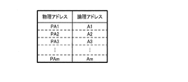
図5、図6、図7は、記憶部120に記憶されるデータの構成(メモリーマップ)を説明する図である。図5は、論理アドレスと、各論理アドレスに対応するデータの構造を表す図であり、図6は論理アドレスと物理アドレスの対応関係を示す図であり、図7は論理ページと論理アドレスの対応関係を示す図である。
5, 6 and 7 are diagrams for explaining the structure (memory map) of data stored in the
図5に示すように、例えば記憶部120は第1〜第m(mは2以上の整数)の論理アドレスA1〜Amを有し、各アドレスに対して32ビットのデータを記憶することができる。A1に示すように、1つの論理アドレスには8ビットのデータが格納されるとともに、他の24ビットを用いて付加的なデータを記憶する。なお、データのビット数は8ビットに限定されず増減が可能である。
As shown in FIG. 5, for example, the
ここでの付加的なデータとは、例えば誤り訂正符号(ECC)である。また、付加的なデータは、ライトロックビットWLCKを含むことができる。ライトロックビットWLCKは、各アドレスに設けられ、そのアドレスに対する書き込み禁止(ライトロック)を設定するためのビットである。例えばアドレスA1のライトロックビットWLCKが1に設定されている場合には、記憶制御部130により、アドレスA1に対する書き込みが禁止される。通常は、ライトロックビットWLCKは工場出荷時に設定され、その後はライトロックビットWLCKを書き換えることはできない。またライトロックビットWLCKを1ビットではなく、複数のビットで構成してもよい。また、付加的なデータとしてECCやライトロックビットWLCK以外のビットを設けてもよい。また、必ず値が‘1’或いは‘0’で固定されるビットを設けてもよい。
The additional data here is, for example, an error correction code (ECC). Also, the additional data may include a write lock bit WLCK. The write lock bit WLCK is provided at each address and is a bit for setting write inhibition (write lock) for the address. For example, when the write lock bit WLCK of the address A1 is set to 1, the
記憶装置100が受信した第1〜第mのデータパケットDPK1〜DPKmは、受信した順番に(シーケンシャルに)、アドレスカウンターADDR_COUNTにより論理アドレスが割り振られる。すなわち第1のデータパケットDPK1は、第1の論理アドレスA1が割り振られ、第2のデータパケットDPK2は、第2の論理アドレスA2が割り振られ、同様にして第3〜第mのデータパケットDPK3〜DPKmは、それぞれ第3〜第mの論理アドレスA3〜Amが割り振られる。この論理アドレスは図1のアドレス情報addrに対応するものであり、制御部110がアドレスカウンターADDR_COUNTに更新指示を行うことで、データパケットを受信する毎にアドレス情報addrが更新(インクリメント)される。
The first to mth data packets DPK1 to DPKm received by the
上述したように、本実施形態の記憶装置及びホスト装置では、書き込みデータパケットDPKのデータパターンが特定パターンと一致している場合には、アドレス情報addrの更新指示(インクリメント)を行うが、書き込みデータの書き込みは行わない。 As described above, in the storage device and the host device of the present embodiment, when the data pattern of the write data packet DPK matches the specific pattern, the update instruction (increment) of the address information addr is issued, but the write data Is not written.
具体的には、制御部110は、コマンドパケットCMPKに対応する第1〜第mのデータパケットDPK1〜DPKmを受信する。第1〜第mの書込みデータパケットDPK1〜DPKmのうち、第i(iは1≦i≦mを満たす整数)の書込みデータパケットは、第iの書き込みデータと、第iの付加データを含む。そして制御部110は、第iの書き込みデータと第iの付加データにより構成されるデータパターンが特定パターンと一致しないと判定された場合は、記憶制御部130に対して、アドレス情報addrの更新指示(例えばインクリメント)を行うとともに、第iの書き込みデータの書き込み指示を行う。第iの書き込みデータと第iの付加データとによって構成されるデータパターンが、特定パターンと一致すると判定された場合は、制御部110は、記憶制御部130に対して、アドレス情報addrの更新指示を行う一方で、第iの書き込みデータの書き込み指示を行わない。
Specifically, the
このようにすることで、記憶装置100は、書き込み非許可に設定されたDPKiのデータの書き込み処理を行わずに、次のデータパケットDPKi+1の受信処理に移行することができ、DPKi+1が書き込み許可である場合には、次の論理アドレスAi+1に対応する物理アドレスに、DPKi+1の書き込みデータD0〜D7を書き込むことができる。
By doing so, the
図6に示した例では、1つの論理アドレスAiが1つの物理アドレスPAiに対応するため、DPKiが書き込み許可である場合には、論理アドレスAiに対応する物理アドレスPAiに、DPKiの書き込みデータD0〜D7を書き込む。図6では、記憶制御部130(狭義には不図示の物理アドレス生成部)は、1つの論理アドレスを1つの物理アドレスに変換する例を説明したがこれには限定されない。記憶制御部130は、1つの論理アドレスに対して、1又は複数の物理アドレスを割り当ててもよい。このようにすれば、所与の論理アドレスに対応付けられたデータを、複数の物理アドレスのうち、あらかじめ決められたルールにより選択された1つの物理アドレスに書き込むことが可能になる。
In the example shown in FIG. 6, one logical address Ai corresponds to one physical address PAi. Therefore, when the DPKi is write-enabled, the write data D0 of the DPKi is written to the physical address PAi corresponding to the logical address Ai. Write ~ D7. In FIG. 6, the storage control unit 130 (a physical address generation unit not shown in a narrow sense) describes an example of converting one logical address into one physical address, but the present invention is not limited to this. The
或いは、記憶制御部130は、図7に示したようにページを単位として、1つの論理ページPに対して複数の論理アドレスを割り当ててもよい。図7の例では、4つの論理アドレスが1つの論理ページに対応付けられる。
Alternatively, the
なお、本実施形態の記憶部の構成は、図5、図6、図7に示した構成に限定されず、その構成要素の一部を省略したり、他の構成要素に置き換えたり、他の構成要素を追加するなどの種々の変形実施が可能である。例えば、1アドレスに記憶されるビット数を増減してもよい。 Note that the configuration of the storage unit of the present embodiment is not limited to the configurations shown in FIGS. 5, 6, and 7, and some of the components may be omitted, replaced with other components, or other components. Various modifications such as addition of components are possible. For example, the number of bits stored in one address may be increased or decreased.
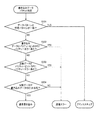
4.書き込み処理
図8は、本実施形態に係る記憶装置100での書き込み処理を説明するフローチャートである。図8の各ステップの処理は、記憶装置100の記憶制御部130により行われる。記憶装置100は、1ページ単位での書き込みを行う不揮発性メモリーであり、図8は1ページ分の書き込み制御を説明する図である。なお、ここでの1ページは、例えば4アドレスに対応する128ビットの領域である。
4. Write Process FIG. 8 is a flowchart illustrating a write process in the
この処理が開始されると、まず記憶制御部130は、通信エラーフラグ及びスキップフラグを初期化する(ステップS101,S102)。通信エラーフラグとは、通信エラーが発生したか否かを表すフラグであり、ステップS101の初期化により通信エラーが発生していないことを表す状態となる。また、スキップフラグとは、各論理アドレスに対応して設けられるフラグであり、対応する論理アドレスが割り当てられる書き込みデータの書き込みをスキップするか(非書き込みとするか)否かを表すフラグである。ステップS102の初期化により、1ページ分の全アドレスについて、書き込みをスキップしない状態が初期状態として設定される。
When this process is started, the
記憶制御部130は、対象としている1ページ分のデータを一時バッファーにコピーする(ステップS103)。
The
そして、記憶制御部130は、制御部110から1アドレス分の書き込みデータパケットの受信結果を取得する(ステップS104)。この際、制御部110では、ホスト装置から受信した書き込みデータパケットDPKに対して、スキップ判定及びエラーチェック(通信エラー判定)を行っている。
Then, the
図9は、制御部110におけるスキップ判定及び通信エラー判定を説明するフローチャートである。この処理が開始されると、制御部110(狭義には比較部COMP)は、書き込みデータD0〜D7と付加データ(パリティービットDP)から構成されるデータパターンが、特定パターン(FFh+‘0’)と一致するかを判定する(ステップS201)。一致する場合には、制御部110は、“アドレススキップ”であると判定して処理を終了する。
FIG. 9 is a flowchart illustrating skip determination and communication error determination in
データパターンと特定パターンが一致しない場合(ステップS201でNoの場合)は、制御部110(狭義にはエラー検出部ERR_DET)は、パリティーエラーであるか否かを判定する(ステップS202)。パリティーエラーが検出された場合は、制御部110は、“通信エラー”であると判定して処理を終了する。
When the data pattern and the specific pattern do not match (No in step S201), the control unit 110 (error detection unit ERR_DET in a narrow sense) determines whether or not there is a parity error (step S202). When the parity error is detected, the
パリティーエラーが検出されない場合(ステップS202でNoの場合)は、制御部110は、“通常書き込み”と判定して処理を終了する。
When the parity error is not detected (No in step S202), the
記憶制御部130は、ステップS104において書き込みデータD0〜D7(data)を受信するとともに、図9に示した処理の判定結果を制御部110から受信する。すなわち、記憶制御部130は、“アドレススキップ”、“通信エラー”、“通常書き込み”のいずれであるかの判定結果を取得する。
The
記憶制御部130は、“アドレススキップ”であるかを判定し(ステップS105)、Noの場合には“通信エラー”であるかを判定する(ステップS106)。“通信エラー”でもない、すなわち“通常書き込み”の場合には、記憶制御部130は、ステップS103で一時バッファーにコピーしておいたデータのうち、対象としているアドレスのデータを受信した書き込みデータにより更新する(ステップS107)。
The
“通信エラー”である場合には、記憶制御部130は、通信エラーフラグを、通信エラーが発生していることを表す状態にセットする(ステップS108)。一方、“アドレススキップ”の場合(ステップS105でYesの場合)は、ステップS107、S108のいずれの処理も行わずに、ステップS109に移行する。これにより、“アクセススキップ”の場合には、制御部110は、一時バッファーの更新なしに、次の書き込みデータパケットの受信を行うことが可能になる。具体的な動作例は、図10のタイミングチャートを用いて後述する。
In the case of "communication error", the
そして、記憶制御部130は全アドレスに対する処理が終了したかを判定し(ステップS109)、終了していない場合には、ステップS104に戻り、処理を継続する。全アドレスに対する処理が終了したら、通信エラーフラグの状態を判定する(ステップS110)。
Then, the
通信エラーフラグがセットされている(通信エラーが発生している)場合は、記憶制御部130は、1ページ分の書き込みが異常終了したと判定する。この場合、制御部110は、ホスト装置に対して通信エラーを通知する。
If the communication error flag is set (a communication error has occurred), the
通信エラーフラグがセットされていない場合(ステップS110でNoの場合)は、記憶制御部130は、スキップフラグを参照し、1ページ分の全アドレスについてスキップフラグがセットされているか否かを判定する(ステップS111)。ステップS111でYesの場合、すなわち全アドレスで非書き込みと判定された場合は、書き込み自体を行う必要がないため、そのまま1ページ分の書き込みを正常終了する。ステップS111でNoの場合は、更新が必要なデータがあるため、対象の1ページのデータを消去し、ステップS107で更新した一時バッファーのデータをメモリーセルアレイ部120の対応する領域に書き込む(S112)。ステップS112の処理後も、記憶制御部130は1ページ分の書き込みを正常終了する。
If the communication error flag is not set (No in step S110), the
図8、図9に示したように、書き込み処理をスキップする場合は、データパターンと特定パターンが一致したことを条件とすればよいが、書き込み処理を実行する場合は、データパターンと特定パターンが不一致であることだけでなく、通信エラーが無いことも条件となる。具体的には、制御部110は、書き込みデータとパリティーデータにより構成されるデータパターンが特定パターンと一致しないと判定され、且つ、書き込みデータとパリティーデータの関係が肯定されている場合は、記憶制御部130に対して、アドレス情報の更新指示を行うとともに、書き込みデータの書き込み指示を行う。また制御部110は、書き込みデータとパリティーデータとによって構成されるデータパターンが、特定パターンと一致すると判定された場合は、記憶制御部130に対して、アドレス情報の更新指示を行う一方で、書き込みデータの書き込み指示を行わない。
As shown in FIGS. 8 and 9, when the writing process is skipped, it is only necessary that the data pattern and the specific pattern match, but when the writing process is executed, the data pattern and the specific pattern are Not only do they not match, but there is no communication error. Specifically, the
このようにすれば、図9に示したように、制御部110において書き込み処理のスキップ判定と、通信エラー判定の両方を実行することが可能になる。
By doing so, as shown in FIG. 9, it becomes possible for the
また、特定パターンはエラーチェックにおいてエラーと判定されるようなデータ構成を用いるため、制御部110は、付加データに基づきエラーを検出したとしても、それだけでは本当に通信エラーなのか、特定パターンとなる書き込みデータパケットを受信したかを判別できない。よって制御部110は、書き込みデータパケットと付加データに基づくエラーチェックにおいてエラーと判定され、且つ、データパターンが特定パターンと一致しないと判定した場合は、ホスト装置400に対してデータエラーを表す情報を送信する。これは、図9で言えば、ステップS201でNo且つステップS202でYesの場合に、“通信エラー”と判定する処理フローに対応する。
In addition, since the specific pattern uses a data structure that is determined to be an error in the error check, the
このようにすれば、“アドレススキップ”と“通信エラー”を適切に判別することが可能になる。 By doing so, it becomes possible to properly discriminate between “address skip” and “communication error”.
図10に、本実施形態の記憶装置100、ホスト装置400の書き込み処理のタイミングチャートを示す。図10には、リセット信号XRST、クロック信号SCK及びデータ信号SDAの各信号波形と、記憶装置100における制御部110、記憶部120の動作状態及び内部信号wr、i_ackの信号波形とを示す。
FIG. 10 shows a timing chart of the write processing of the
図10において、Iはアイドル期間、IDCはID認識期間、CMDはコマンド認識期間、DATはデータ受信期間、IAKWは内部アクノリッジ待ち期間、MWRTはメモリー書き込み期間、AKSはアクノリッジ返信期間、NWは、受信したデータパケットが書き込み非許可に設定されている場合で、書き込み処理を行わずに、通信エラーの有無を判断する期間である。なお、ここでは図7を用いて上述したように、1ページが4つの論理アドレスに対応する例を説明する。また、図8のフローチャートを用いて上述したように、書き込みスキップを行うか否かは、書き込み単位である1ページ分のデータを用いて判定する例を説明する。 In FIG. 10, I is an idle period, IDC is an ID recognition period, CMD is a command recognition period, DAT is a data reception period, IAKW is an internal acknowledge wait period, MWRT is a memory write period, AKS is an acknowledge reply period, and NW is a reception period. This is a period in which the presence or absence of a communication error is determined without performing the writing process when the writing data packet is set to write-disabled. Note that, here, as described above with reference to FIG. 7, an example in which one page corresponds to four logical addresses will be described. Further, as described above with reference to the flowchart of FIG. 8, an example will be described in which whether or not to perform the write skip is determined using the data of one page which is the write unit.
図10の例では、第1〜第4のデータパケットDPK1〜DPK4、及び第9〜第12のデータパケットDPK9〜DPK12の全ての書き込みデータがFFh(‘11111111’)、パリティービットDPが‘0’に設定される。すなわち、第1〜第4のデータパケットDPK1〜DPK4、及び第9〜第12のデータパケットDPK9〜DPK12はデータパターンが特定パターンと一致するように設定される。一方、第5〜第8のデータパケットDPK5〜DPK8及び第13〜第16のデータパケットDPK13〜DPK16では、4つのデータパケットのうちの少なくとも1つのデータパケットのデータパターンは、特定パターンと一致しないように設定されている。 In the example of FIG. 10, all the write data of the first to fourth data packets DPK1 to DPK4 and the ninth to twelfth data packets DPK9 to DPK12 are FFh ('11111111') and the parity bit DP is '0'. Is set to. That is, the first to fourth data packets DPK1 to DPK4 and the ninth to twelfth data packets DPK9 to DPK12 are set so that the data pattern matches the specific pattern. On the other hand, in the fifth to eighth data packets DPK5 to DPK8 and the thirteenth to sixteenth data packets DPK13 to DPK16, the data pattern of at least one of the four data packets does not match the specific pattern. Is set to.
最初に、ホスト装置400は、リセット信号XRSTをLレベル(低電位レベル、広義には第2の論理レベル)からHレベル(高電位レベル、広義には第1の論理レベル)に設定して記憶装置のリセットを解除する。そして制御部110は、アイドル状態になる。
First, the
次にホスト装置400は、記憶装置100に対してIDパケットIDPK、コマンドパケットCMPK及びデータパケットDPK1〜DPK4を送信し、その後に記憶装置100からのアクノリッジACK返信を待つステートに移行する。
Next, the
記憶装置100のIDコンパレーターID_COMPは、ID認識期間IDCにおいて、受信したID情報と自身のID情報とが一致することを認識する。続くコマンド認識期間CMDにおいて、オペレーションコードデコーダーOPCDECは、受信したコマンドが書き込みコマンドであることを認識する。次のデータ受信期間DATにおいて、I/OコントローラーI/O_CNTLは、書き込みデータパケットDPK1〜DPK4を受信し、比較部COMPは、書き込みデータパケットのデータパターンが特定パターンと一致するか否かを判断する。具体的には、第1〜第4のデータパケットDPK1〜DPK4のそれぞれについて、データパターンが特定パターンと一致するか否かを判断する。
The ID comparator ID_COMP of the
図10に示すように、DPK1〜DPK4の全てのデータパケットについて、データパターンと特定パターンが一致する場合には、制御部110は書き込み指示を記憶制御部130に対して行わない。そして制御部110は、通信エラーの有無をチェックして、通信エラーが無いと判断された場合にはホスト装置400に対してアクノリッジACKを返信する。ホスト装置400は、通信エラーが無いことを通知するアクノリッジACKを受け取った後、第2のページに対応するデータパケット(第5〜第8のデータパケットDPK5〜DPK8)を送信する。
As shown in FIG. 10, when the data pattern and the specific pattern match for all the data packets of DPK1 to DPK4, the
制御部110は、第1〜第4のデータパケットDPK1〜DPK4(広義には第iのページに対応するデータパケット)が書き込み非許可状態に設定されている場合には、記憶制御部130からの内部アクノリッジi_ackを待たずに次のページのデータパケットDPK5〜DPK8(広義には第i+1のページに対応するデータパケット)の受信処理を行う。
When the first to fourth data packets DPK1 to DPK4 (data packets corresponding to the i-th page in a broad sense) are set in the write non-permission state, the
第5〜第8のデータパケットDPK5〜DPK8は、少なくとも1つのデータパケットのデータパターンが特定パターンと一致しないように設定されているから、制御部110は、DPK5〜DPK8の受信後に書き込み指示wrを記憶制御部130に対して行う。記憶部120は、書き込み指示wrに基づいて、メモリー書き込み期間MWRTにおいて、データを書き込む。このメモリー書き込み期間MWRTにおいて、制御部110は内部アクノリッジ待ち期間IAKWとなり、記憶制御部130から内部アクノリッジ信号i_ackが出力されるのを待つ。データが正常に書き込まれた場合には、記憶制御部130は、内部アクノリッジ信号i_ackを制御部110に出力する。制御部110は、内部アクノリッジ信号i_ackを受け取ると、ホスト装置400に対してアクノリッジACKを返信する。ホスト装置400は、アクノリッジACKを受け取った後、第3のページに対応するデータパケット(DPK9〜DPK12)を送信する。
Since the fifth to eighth data packets DPK5 to DPK8 are set so that the data pattern of at least one data packet does not match the specific pattern, the
図10の例では、DPK9〜DPK12の全てのデータパケットが書き込み非許可状態に設定されているから、制御部110は、DPK9〜DPK12の受信後、通信エラーの有無をチェックして、通信エラーが無いと判断された場合にはホスト装置400に対してアクノリッジACKを返信する。ホスト装置400は、通信エラーが無いことを通知するアクノリッジACKを受け取った後、第4のページに対応するデータパケット(DPK13〜DPK16)を送信する。
In the example of FIG. 10, since all the data packets of DPK9 to DPK12 are set to the write non-permission state, the
DPK13〜DPK16のうちの少なくとも1つのデータパケットは書き込み許可状態に設定されているから、制御部110は、DPK13〜DPK16の受信後に書き込み指示wrを記憶制御部130に対して行う。記憶部120は、書き込み指示wrに基づいて、メモリー書き込み期間MWRTにおいて、データを書き込む。データが正常に書き込まれた場合には、記憶制御部130は、内部アクノリッジ信号i_ackを制御部110に出力する。制御部110は、内部アクノリッジ信号i_ackを受け取ると、ホスト装置400に対してアクノリッジACKを返信する。
Since at least one data packet of the DPK13 to DPK16 is set to the write enable state, the
図11に、比較例として、書き込みスキップを行わない場合の、書き込み処理のタイミングチャートを示す。図11の比較例では、m個のページに対応するデータパケット(DPK1〜DPK4、DPK5〜DPK8、…、DPK4m−3〜DPK4m)のそれぞれについてメモリー書き込み期間MWRTが必要である。データパケットの送信に要する時間は、例えば約100μs程度であるのに対して、メモリー書き込み期間MWRTの長さTM(書き込み必要時間)は、約5msである。従って、mページのデータパケットDPK1〜DPK4mを書き込む場合の書き込み処理時間は少なくともm×TMとなる。 As a comparative example, FIG. 11 shows a timing chart of the writing process when the writing skip is not performed. In the comparative example of FIG. 11, the memory write period MWRT is required for each of the data packets (DPK1 to DPK4, DPK5 to DPK8, ..., DPK4m-3 to DPK4m) corresponding to m pages. The time required for transmitting the data packet is, for example, about 100 μs, while the length TM (writing required time) of the memory writing period MWRT is about 5 ms. Therefore, the write processing time when writing the data packets DPK1 to DPK4m of m pages is at least m × TM.
一方、本実施形態の記憶装置100、ホスト装置400によれば、書き込む必要のあるデータパケットを選択して書き込むことができる。すなわち、データパターンと特定パターンが一致しないように設定した書き込みデータパケット(具体的には当該書き込みデータパケットを含む1ページ分のデータ)に限定してデータを書き込むことができるから、書き込み処理時間を短縮することができる。
On the other hand, according to the
5.システム、液体装置及び回路基板
図12に本実施形態のシステムの基本的な構成例を示す。本実施形態のシステムは、例えばインクジェット方式のプリンターなどであって、第1の記憶装置100−1〜第n(nは2以上の整数)の記憶装置100−n、記憶装置が実装されるn個の回路基板200−1〜200−n、回路基板を備えるn個の液体容器300−1〜300−n及びホスト装置400を含む。なお、本実施形態のシステムは図12の構成に限定されず、その構成要素の一部を省略したり、他の構成要素に置き換えたり、他の構成要素を追加するなどの種々の変形実施が可能である。
5. System, Liquid Device, and Circuit Board FIG. 12 shows a basic configuration example of the system of this embodiment. The system according to the present embodiment is, for example, an inkjet printer, and includes the first storage device 100-1 to the n-th storage device 100-n (n is an integer of 2 or more), and the storage device is mounted n. The circuit boards 200-1 to 200-n, the n liquid containers 300-1 to 300-n including the circuit boards, and the
以下では、ホスト装置400がインクジェット方式のプリンター本体であり、液体容器300がインクカートリッジであり、回路基板200がインクカートリッジに設けられた回路基板である場合を例に説明する。但し、本実施形態では、ホスト装置、液体容器、回路基板は、他の装置、容器、回路基板であってもよい。例えば、ホスト装置はメモリーカードのリーダー/ライターであってもよく、回路基板はメモリーカードに設けられた回路基板であってもよい。
Hereinafter, a case where the
第1の記憶装置100−1〜第nの記憶装置100−nは、それぞれリセット端子TRST、クロック端子TCK、データ端子TDA、第1の電源端子VDD及び第2の電源端子VSSを含む。これらn個の記憶装置100−1〜100−nの各々は、記憶部120(例えば不揮発性メモリー等)を含み、それぞれの記憶部120にはn個の液体容器(例えばインクカートリッジ等)300−1〜300−nを識別するためのID(Identification)情報(例えばID=1、ID=2、ID=3など)が記憶されている。IDは、液体容器が収容する液体の色などの種類毎に異なるものが付与される。また記憶部120には、液体容器のインク残量(又はインク消費量)などのデータが、ホスト装置400により書き込まれる。
Each of the first memory device 100-1 to the nth memory device 100-n includes a reset terminal TRST, a clock terminal TCK, a data terminal TDA, a first power supply terminal VDD, and a second power supply terminal VSS. Each of the n storage devices 100-1 to 100-n includes a storage unit 120 (for example, a non-volatile memory or the like), and each
ホスト装置400は、例えばプリンター本体などであって、ホスト側リセット端子HRST、ホスト側クロック端子HCK、ホスト側データ端子HDA、第1の電源端子VDD及び第2の電源端子VSSを含む。
The
上述したように、本実施形態の記憶装置100、ホスト装置400及びシステムによれば、ホスト装置400から記憶装置100に対して送信される書き込みデータパケットのデータパターンを用いて、書き込みデータの書き込み許可状態又は非許可状態を設定することができる。
As described above, according to the
そして記憶装置100は、受信した書き込みデータパケットのデータパターンと特定パターンの比較処理に基づいて、そのデータを記憶部120に書き込むか否かを判断し、書き込み非許可の場合にはデータを書き込まずに、次のデータパケットの受信処理及び書き込み処理に移行することができる。すなわち、書き込む必要のない書き込みデータパケットについてはデータの書き込みをスキップして、次の書き込みデータパケットの処理に移行することができる。その結果、記憶装置100に対するデータ書き込み処理の時間を短縮することができる。また書き込む必要のないデータについては、書き込み処理を行わないから、既に記憶されているデータを書き込み時のエラー等により破壊するおそれを低減することができる。
Then, the
図13に、本実施形態の液体容器(インクカートリッジ)300の詳細な構成例を示す。液体容器300の内部には、インクを収容するための図示しないインク室が形成される。また、液体容器300には、インク室に連通するインク供給口340が設けられる。このインク供給口340は、液体容器300がプリンターに装着された時に、印刷ヘッドユニットにインクを供給するためのものである。
FIG. 13 shows a detailed configuration example of the liquid container (ink cartridge) 300 of this embodiment. An ink chamber (not shown) for containing ink is formed inside the
液体容器300は、回路基板200を含む。回路基板200には、本実施形態の記憶装置100が設けられ、インク消費量などのデータの記憶やホスト装置400とのデータ送受信を行う。回路基板200は、例えばプリント基板により実現され、液体容器300の表面に設けられる。回路基板200には、第1の電源端子VDD等の端子が設けられる。そして、液体容器300がプリンターに装着された時に、それらの端子とプリンター側の端子が接触(電気的に接続)することで、電源やデータのやり取りが行われる。
The
図14、図15に、本実施形態の記憶装置100が設けられた回路基板200の詳細な構成例を示す。図14に示すように、回路基板200の表面(プリンターと接続される面)には、複数の端子を有する端子群が設けられる。この端子群は、第1の電源端子VDD、第2の電源端子VSS、リセット端子TRST、クロック端子TCK、データ端子TDAを含む。各端子は、例えば矩形状(略矩形状)に形成された金属端子により実現される。そして、各端子は、回路基板200に設けられた図示しない配線パターン層やスルーホールを介して、記憶装置100に接続される。
14 and 15 show detailed configuration examples of the
図15に示すように、回路基板200の裏面(プリンターと接続される面の裏側の面)には、本実施形態の記憶装置100が設けられる。記憶装置100は、例えば、MONOS型メモリーを有する半導体記憶装置により実現できる。この記憶装置100には、インク又は液体容器300に関連する種々のデータが格納され、例えば、液体容器300を識別するためのID情報やインクの消費量等のデータが格納される。インク消費量のデータは、液体容器300内に収容されたインクについて、印刷の実行等に伴い消費されるインク量の累計を示すデータである。このインク消費量のデータは、液体容器300内のインク量を示す情報であってもよく、消費したインク量の割合を示す情報であってもよい。
As shown in FIG. 15, the
6.変形例
以上では、書き込みデータパケットが8ビットの書き込みデータと1ビットのパリティービットである付加データとにより構成されるものとしたが、これには限定されない。図16に通信パケットの変形例を示す。
6. Modifications In the above description, the write data packet is composed of write data of 8 bits and additional data of 1 bit of parity bit, but the present invention is not limited to this. FIG. 16 shows a modification of the communication packet.
図16に示したように、書き込みデータパケットは、付加データとして書き込みデータの反転データを含んでもよい。D0〜D7が書き込みデータであり、/D0〜/D7が反転データである。ここでの反転データとは、各ビットの値の0と1とが反転したデータであり、書き込みデータで‘1’であるビットは反転データでは‘0’となり、書き込みデータで‘0’であるビットは反転データでは‘1’となる。例えば、書き込みデータがFFh(‘11111111’)であれば、反転データは00h(‘00000000’)となる。
As shown in FIG. 16, the write data packet may include inverted data of the write data as additional data. D0 to D7 are write data, and / D0 to / D7 are inverted data. The inverted data here is data in which the
反転データは、書き込みデータのエラーチェックに用いられる情報である。具体的には、制御部110は、書き込みデータと反転データを取得し、反転データが、書き込みデータがビット反転されたデータであるか否かを判定する。例えば、制御部110(エラー検出部ERR_DET)は、書き込みデータと反転データのXOR(排他的論理和)と、FFh(‘11111111’)が一致するか否かを判定する。正常状態では、書き込みデータと反転データのXORと、FFhが一致するため、制御部110は、一致した場合は通信エラーでないと判定し、一致しない場合は通信エラーであると判定する。
The inverted data is information used for error check of the write data. Specifically, the
この場合、書き込みデータと付加データ(反転データ)により構成されるデータパターンは16ビットとなるため、特定パターンも16ビットとなる。また、書き込みを意図しているデータと特定パターンとが一致することは好ましくないため、特定パターンはエラーチェックによりエラーと判定されるデータとする。 In this case, since the data pattern composed of the write data and the additional data (inverted data) has 16 bits, the specific pattern also has 16 bits. Further, since it is not preferable that the data intended for writing and the specific pattern match, the specific pattern is data determined to be an error by an error check.
具体的には、特定パターンは、第1のデータと、第1のデータの反転データではない第2のデータにより構成されるパターンとする。例えばFFh+FFh(‘1111111111111111’)を特定パターンとすればよい。 Specifically, the specific pattern is a pattern composed of the first data and the second data that is not the inverted data of the first data. For example, FFh + FFh ('11111111111111111') may be used as the specific pattern.
ホスト装置400は、書き込み処理を行う書き込みデータパケットは、書き込みデータとその反転データを含むように設定し、書き込み処理を行わない書き込みデータパケットは、FFh+FFhとなるように設定する。
The
記憶装置100では、受信した書き込みデータパケットのデータパターンと、特定パターン(FFh+FFh)を比較する。具体的には、制御部110は、書き込みデータと反転データにより構成されるデータパターンが特定パターンと一致しないと判定された場合は、記憶制御部130に対して、アドレス情報の更新指示を行うとともに、書き込みデータの書き込み指示を行い、書き込みデータと反転データとによって構成されるデータパターンが、特定パターンと一致すると判定された場合は、記憶制御部130に対して、アドレス情報の更新指示を行う一方で、書き込みデータの書き込み指示を行わない。
The
この場合も、制御部110は、書き込みイネーブルビットWEを用いることなく、書き込み/非書き込みを判定できる。また、多数のビットに通信エラーが発生しない限り、書き込みを意図した書き込みデータパケットのデータパターンが、特定パターンと一致することはない。例えば、書き込みデータがFFhの場合、反転データは00hとなるため、これが通信エラーによりFFh+FFhと一致する場合には、8ビットにエラーが発生していることになる。多数のビットに通信エラーが発生する可能性は非常に低いため、記憶装置100では、書き込み処理の対象の書き込みデータパケットを誤って非書き込みとしてしまう可能性を抑止できる。
Also in this case, the
なお、図16に示したように、書き込みデータパケットは、付加データとしてパリティーデータ及び書き込みデータの反転データを含んでもよい。図16の例では、書き込みデータパケットは、書き込みデータD0〜D7と、書き込みデータのパリティービットDPと、反転データ/D0〜/D7と、反転データのパリティービット/DPを含む。 As shown in FIG. 16, the write data packet may include parity data and inverted data of the write data as additional data. In the example of FIG. 16, the write data packet includes write data D0 to D7, write data parity bits DP, inverted data / D0 to / D7, and inverted data parity bits / DP.
ここでパリティービットDPは、書き込みデータD0〜D7とパリティービットDPの9ビットにおいて、‘1’となるビット数が奇数(奇数パリティーの場合)となるように設定されるビットである。また、パリティービット/DPは、反転データ/D0〜/D7とパリティービット/DPの9ビットにおいて、‘1’となるビット数が奇数となるように設定されるビットである。つまり、/DPはDPがビット反転されたデータではない。 Here, the parity bit DP is a bit that is set so that the number of bits that become “1” in the 9 bits of the write data D0 to D7 and the parity bit DP is odd (in the case of odd parity). Further, the parity bit / DP is a bit set so that the number of bits of "1" in the 9 bits of the inverted data / D0 to / D7 and the parity bit / DP is an odd number. That is, / DP is not the bit-inverted data of DP.
この場合、書き込みデータと付加データ(反転データ及びパリティービット)により構成されるデータパターンは18ビットとなるため、特定パターンも18ビットとなる。特定パターンは、第1のデータと、第1のデータの反転データではない第2のデータと、エラーチェックによりパリティーエラーと判定されるビットと、により構成されるパターンとする。例えばFFh+‘0’+FFh+‘0’(‘111111110111111110’)を特定パターンとすればよい。 In this case, since the data pattern formed by the write data and the additional data (inversion data and parity bit) has 18 bits, the specific pattern also has 18 bits. The specific pattern is a pattern composed of the first data, the second data that is not the inverted data of the first data, and the bit determined to be the parity error by the error check. For example, FFh + '0' + FFh + '0' ('111111110111111110') may be set as the specific pattern.
記憶装置100では、受信した書き込みデータパケットのデータパターンと、特定パターン(FFh+‘0’+FFh+‘0’)を比較する。具体的には、制御部110は、書き込みデータ、パリティーデータ及び反転データにより構成されるデータパターンが特定パターンと一致しないと判定され、且つ、書き込みデータとパリティーデータの関係が肯定されている場合は、記憶制御部130に対して、アドレス情報の更新指示を行うとともに、書き込みデータの書き込み指示を行う。また制御部110は、書き込みデータ、パリティーデータ及び反転データによって構成されるデータパターンが、特定パターンと一致すると判定された場合は、記憶制御部130に対して、アドレス情報の更新指示を行う一方で、書き込みデータの書き込み指示を行わない。
The
このようにすれば、制御部110は、反転データとパリティービットの両方をエラーチェックに用いるため、精度よく通信エラーを検出できる。また、通信エラーにより偶発的に書き込みデータパケットのデータパターンが特定パターンと一致してしまう可能性を抑止できるため、書き込み対象である書き込みデータパケットを非書き込みであると誤判定する可能性を抑止できる。
With this configuration, the
図16のデータを用いる場合の、制御部110でのエラーチェック、スキップ判定を説明するフローチャートを図17に示す。この処理が開始されると、制御部110(比較部COMP)は、データパターンと特定パターンが一致するかを判定する(ステップS301)。一致する場合には、制御部110は、“アドレススキップ”と判定する。
FIG. 17 shows a flowchart for explaining the error check and skip determination in the
一致しない場合には、制御部110(エラー検出部ERR_DET)は、書き込みデータD0〜D7と、パリティービットDPを用いたパリティーチェックを行いエラーがないかを判定する(ステップS302)。エラーが検出された場合には、制御部110は、“通信エラー”であると判定する。
If they do not match, the control unit 110 (error detection unit ERR_DET) determines whether or not there is an error by performing a parity check using the write data D0 to D7 and the parity bit DP (step S302). When an error is detected,
ステップS302でパリティーエラーでない場合には、反転データ/D0〜/D7と、パリティービット/DPを用いたパリティーチェックを行いエラーがないかを判定する(ステップS303)。エラーが検出された場合には、制御部110は、“通信エラー”であると判定する。
If no parity error is found in step S302, a parity check using inverted data / D0 to / D7 and parity bit / DP is performed to determine whether there is an error (step S303). When an error is detected,
ステップS302でパリティーエラーでない場合には、制御部110は、反転データが書き込みデータのビット反転であるかを判定する(ステップS304)。例えば上述したように、書き込みデータと反転データのXORと、FFhとの比較処理を行えばよい。反転データが書き込みデータのビット反転でない場合は、制御部110は、“通信エラー”であると判定する。反転データが書き込みデータのビット反転である場合(ステップS304でYesの場合)は、制御部110は、“通常書き込み”であると判定する。
When the parity error is not generated in step S302, the
なお、この場合、図9に示した処理を図17に示した処理に置き換えればよく、記憶制御部130で行われる処理の流れは、図8と同様である。
In this case, the process shown in FIG. 9 may be replaced with the process shown in FIG. 17, and the flow of the process performed by the
また、以上では特定パターンのうち、書き込みデータに対応するビット(第1のデータ)の値がFFhであるものとしたがこれには限定されず、00h〜FFhの任意の値を第1のデータとして用いることが可能である。その場合、特定パターンのうちの付加データに対応するビット(第2のデータ)の値は、書き込みデータに対応するビットの値に応じて決定すればよい。 Further, in the above description, the value of the bit (first data) corresponding to the write data in the specific pattern is FFh, but the value is not limited to this, and any value from 00h to FFh can be used as the first data. Can be used as In that case, the value of the bit (second data) corresponding to the additional data in the specific pattern may be determined according to the value of the bit corresponding to the write data.
付加データが奇数パリティーのパリティービットである場合、第1のデータが00hであれば、第2のデータはパリティーエラーと判定されるビット、すなわち‘0’とすればよく、特定パターンは00h+‘0’となる。同様に第1のデータが01h(‘00000001’)であれば、第2のデータを‘1’とし、特定パターンは01h+‘1’(‘000000011’)となる。その他、第1のデータがどのような値であっても、対応する特定パターンを設定可能である。 When the additional data is a parity bit of odd parity, if the first data is 00h, the second data may be a bit determined as a parity error, that is, "0", and the specific pattern is 00h + '0. 'Becomes. Similarly, if the first data is 01h ('00000001'), the second data is '1' and the specific pattern is 01h + '1' ('000000011'). In addition, the corresponding specific pattern can be set regardless of the value of the first data.
また、付加データが書き込みデータの反転データである場合、第1のデータが00hであれば、第2のデータはビット反転でないデータ、例えば00hとすればよく、特定パターンは00h+00hとなる。同様に第1のデータが01hであれば、第2のデータを01hとし、特定パターンは01h+01hとなる。この場合も、第1のデータがどのような値であっても、対応する特定パターンを設定可能である。また、付加データが書き込みデータの反転データとパリティービットである場合も同様である。 When the additional data is the inverted data of the write data, if the first data is 00h, the second data may be non-bit-inverted data, for example, 00h, and the specific pattern is 00h + 00h. Similarly, if the first data is 01h, the second data is 01h and the specific pattern is 01h + 01h. Also in this case, the corresponding specific pattern can be set regardless of the value of the first data. The same applies when the additional data is the inverted data of the write data and the parity bit.
また、特定パターンは1つの固定値に限定されず、複数の固定の特定パターンを用いることが可能である。その場合、制御部110は、複数の特定パターンを同時に用いてもよい。具体的には、制御部110は、データパターンが複数の特定パターンのいずれかに一致する場合に、書き込みデータパケットの書き込み処理をスキップする。ただし、同時に用いる特定パターンの数を増やすことで、書き込み処理を行う書き込みデータパケットを誤って非書き込みとしてしまう可能性が増してしまう。よって、制御部110では、複数の特定パターンを用意しておき、そのうちの少数(狭義には1つ)を選択して用いてもよい。
The specific pattern is not limited to one fixed value, and a plurality of fixed specific patterns can be used. In that case, the
なお、書き込み処理のスキップとは直接関係しないが、図16に示したように、通信パケットに含まれるIDパケットIDPK及びコマンドパケットCMPKについても、反転データを含む構成とすることが可能である。このようにすれば、記憶装置100の制御部110では、IDパケットIDPK及びコマンドパケットCMPKに関する通信エラーも精度よく検出することが可能になる。
Although not directly related to the skip of the writing process, as shown in FIG. 16, the ID packet IDPK and the command packet CMPK included in the communication packet can also be configured to include inverted data. With this configuration, the
なお、以上のように本実施形態及び変形例について詳細に説明したが、本発明の新規事項および効果から実体的に逸脱しない多くの変形が可能であることは当業者には容易に理解できるであろう。従って、このような変形例はすべて本発明の範囲に含まれるものとする。例えば、明細書又は図面において、少なくとも一度、より広義または同義な異なる用語と共に記載された用語は、明細書又は図面のいかなる箇所においても、その異なる用語に置き換えることができる。また記憶装置、ホスト装置の構成、動作も本実施形態で説明したものに限定されず、種々の変形実施が可能である。 Although the present embodiment and the modified examples have been described above in detail, those skilled in the art can easily understand that many modifications can be made without departing from the novel matters and effects of the present invention. Ah Therefore, all such modifications are included in the scope of the present invention. For example, a term described in the specification or the drawings at least once together with a different term having a broader meaning or the same meaning can be replaced with the different term anywhere in the specification or the drawing. Further, the configurations and operations of the storage device and the host device are not limited to those described in this embodiment, and various modifications can be made.
ADDR_COUNT…アドレスカウンター、BS…バス、
CMPK…コマンドパケット、COMP…比較部、DPK…データパケット、
ERR_DET…エラー検出部、HCK…クロック端子、HDA…データ端子、
HRST…リセット端子、I/O_CNTL…I/Oコントローラー、
ID_COMP…IDコンパレーター、IDPK…IDパケット、
OPCDEC…オペレーションコードデコーダー、SCK…クロック信号線、
SDA…データ信号線、TCK…クロック端子、TDA…データ端子、
TRST…リセット端子、XRST…リセット信号線、100…記憶装置、
110…制御部、120…記憶部、130…記憶制御部、200…回路基板、
300…液体容器、340…インク供給口、400…ホスト装置、410…通信処理部、
420…制御部
ADDR_COUNT ... address counter, BS ... bus,
CMPK ... command packet, COMP ... comparison unit, DPK ... data packet,
ERR_DET ... error detector, HCK ... clock terminal, HDA ... data terminal,
HRST ... Reset terminal, I / O_CNTL ... I / O controller,
ID_COMP ... ID comparator, IDPK ... ID packet,
OPCDEC ... Operation code decoder, SCK ... Clock signal line,
SDA ... data signal line, TCK ... clock terminal, TDA ... data terminal,
TRST ... Reset terminal, XRST ... Reset signal line, 100 ... Storage device,
110 ... Control unit, 120 ... Storage unit, 130 ... Storage control unit, 200 ... Circuit board,
300 ... Liquid container, 340 ... Ink supply port, 400 ... Host device, 410 ... Communication processing unit,
420 ... Control unit
Claims (10)
前記ホスト装置から送信された書き込みデータパケットに含まれる書き込みデータが書き込まれる記憶部と、
前記記憶部のアクセス制御を行う記憶制御部と、
を含み、
前記制御部は、
前記ホスト装置から、前記書き込みデータパケットを受信し、
前記書き込みデータパケットに含まれる前記書き込みデータと付加データとによって構成されるデータパターンが、特定パターンと一致しないと判定された場合は、前記記憶制御部に対して、前記書き込みデータを前記記憶部に書き込む際のアドレスを特定する情報であるアドレス情報の更新指示を行うとともに、前記書き込みデータの書き込み指示を行い、
前記書き込みデータと前記付加データとによって構成される前記データパターンが、前記特定パターンと一致すると判定された場合は、前記記憶制御部に対して、前記アドレス情報の更新指示を行う一方で、前記書き込みデータの書き込み指示を行わず、
前記付加データは、前記書き込みデータのエラーチェック用のデータであり、
前記特定パターンは、前記エラーチェックにおいてエラーと判定されるデータであることを特徴とする記憶装置。 A control unit that performs communication processing with the host device,
A storage unit in which write data included in the write data packet transmitted from the host device is written,
A storage control unit that controls access to the storage unit;
Including,
The control unit is
Receiving the write data packet from the host device,
When it is determined that the data pattern configured by the write data and the additional data included in the write data packet does not match the specific pattern, the write control unit writes the write data to the storage unit. In addition to giving an instruction to update the address information, which is the information for specifying the address at the time of writing, the writing instruction of the write data
When it is determined that the data pattern formed by the write data and the additional data matches the specific pattern, the storage controller is instructed to update the address information while the write data is written. Without instructing to write data,
The additional data is data for error check of the write data,
The storage device, wherein the specific pattern is data determined to be an error in the error check.
前記制御部は、
前記書き込みデータパケットと前記付加データに基づく前記エラーチェックにおいてエラーと判定され、且つ、前記データパターンが前記特定パターンと一致しないと判定した場合は、前記ホスト装置に対してデータエラーを表す情報を送信することを特徴とする記憶装置。 In claim 1,
The control unit is
When it is determined that an error has occurred in the error check based on the write data packet and the additional data, and it is determined that the data pattern does not match the specific pattern, information indicating a data error is transmitted to the host device. A storage device characterized by:
前記書き込みデータパケットは、前記付加データとしてパリティーデータを含み、
前記制御部は、
前記書き込みデータと前記パリティーデータにより構成される前記データパターンが前記特定パターンと一致しないと判定され、且つ、前記書き込みデータと前記パリティーデータの関係が肯定されている場合は、前記記憶制御部に対して、前記アドレス情報の更新指示を行うとともに、前記書き込みデータの書き込み指示を行い、
前記書き込みデータと前記パリティーデータとによって構成される前記データパターンが、前記特定パターンと一致すると判定された場合は、前記記憶制御部に対して、前記アドレス情報の更新指示を行う一方で、前記書き込みデータの書き込み指示を行わないことを特徴とする記憶装置。 In claim 1 or 2,
The write data packet includes parity data as the additional data,
The control unit is
When it is determined that the data pattern configured by the write data and the parity data does not match the specific pattern, and the relationship between the write data and the parity data is affirmed, the storage controller is notified. The update instruction of the address information and the write instruction of the write data,
When it is determined that the data pattern formed by the write data and the parity data matches the specific pattern, the storage controller is instructed to update the address information while the write data is written. A storage device characterized by not giving a data write instruction.
前記書き込みデータパケットは、前記付加データとして前記書き込みデータの反転データを含み、
前記制御部は、
前記書き込みデータと前記反転データにより構成される前記データパターンが前記特定パターンと一致しないと判定された場合は、前記記憶制御部に対して、前記アドレス情報の更新指示を行うとともに、前記書き込みデータの書き込み指示を行い、
前記書き込みデータと前記反転データとによって構成される前記データパターンが、前記特定パターンと一致すると判定された場合は、前記記憶制御部に対して、前記アドレス情報の更新指示を行う一方で、前記書き込みデータの書き込み指示を行わないことを特徴とする記憶装置。 In claim 1 or 2,
The write data packet includes inverted data of the write data as the additional data,
The control unit is
When it is determined that the data pattern formed by the write data and the inverted data does not match the specific pattern, the storage controller is instructed to update the address information and the write data Write instructions,
When it is determined that the data pattern composed of the write data and the inverted data matches the specific pattern, the storage controller is instructed to update the address information while the write data is written. A storage device characterized by not giving a data write instruction.
前記特定パターンは、第1のデータと、前記第1のデータの反転データではない第2のデータにより構成されるパターンであることを特徴とする記憶装置。 In claim 4,
The storage device, wherein the specific pattern is a pattern composed of first data and second data that is not inverted data of the first data.
前記書き込みデータパケットは、前記付加データとしてパリティーデータ及び前記書き込みデータの反転データを含み、
前記制御部は、
前記書き込みデータ、前記パリティーデータ及び前記反転データにより構成される前記データパターンが前記特定パターンと一致しないと判定され、且つ、前記書き込みデータと前記パリティーデータの関係が肯定されている場合は、前記記憶制御部に対して、前記アドレス情報の更新指示を行うとともに、前記書き込みデータの書き込み指示を行い、
前記書き込みデータ、前記パリティーデータ及び前記反転データによって構成される前記データパターンが、前記特定パターンと一致すると判定された場合は、前記記憶制御部に対して、前記アドレス情報の更新指示を行う一方で、前記書き込みデータの書き込み指示を行わないことを特徴とする記憶装置。 In claim 1 or 2,
The write data packet includes parity data and inverted data of the write data as the additional data,
The control unit is
If it is determined that the data pattern composed of the write data, the parity data, and the inversion data does not match the specific pattern, and the relationship between the write data and the parity data is affirmed, the storage The controller is instructed to update the address information and the write data is instructed,
When it is determined that the data pattern composed of the write data, the parity data, and the inverted data matches the specific pattern, the storage controller is instructed to update the address information. A storage device which does not issue a write instruction of the write data.
前記制御部は、
コマンドパケットに対する前記書き込みデータパケットとして、第1〜第m(mは2以上の整数)の書込みデータパケットを受信し、
前記第1〜第mの書込みデータパケットのうち、第i(iは1≦i≦mを満たす整数)の書込みデータパケットは、第iの書き込みデータと、第iの付加データを含み、
前記第iの書き込みデータと前記第iの付加データにより構成される前記データパターンが前記特定パターンと一致しないと判定された場合は、前記記憶制御部に対して、前記アドレス情報の更新指示を行うとともに、前記第iの書き込みデータの書き込み指示を行い、
前記第iの書き込みデータと前記第iの付加データとによって構成される前記データパターンが、前記特定パターンと一致すると判定された場合は、前記記憶制御部に対して、前記アドレス情報の更新指示を行う一方で、前記第iの書き込みデータの書き込み指示を
行わないことを特徴とする記憶装置。 In any one of Claim 1 thru | or 6,
The control unit is
The first to mth (m is an integer of 2 or more) write data packets are received as the write data packets for the command packet,
Of the first to m-th write data packets, the i-th (i is an integer satisfying 1 ≦ i ≦ m) write data packet includes the i-th write data and the i-th additional data.
When it is determined that the data pattern formed by the i-th write data and the i-th additional data does not match the specific pattern, the storage controller is instructed to update the address information. At the same time, the write instruction of the i-th write data is given,
When it is determined that the data pattern composed of the i-th write data and the i-th additional data matches the specific pattern, the storage controller is instructed to update the address information. A storage device, characterized in that the write instruction of the i-th write data is not issued while performing the write operation.
前記制御部は、
前記データパターンと前記特定パターンとを比較する比較部と、
前記付加データに基づくエラーチェックを行うエラー検出部と、
を含むことを特徴とする記憶装置。 In any one of Claim 1 thru | or 7,
The control unit is
A comparison unit that compares the data pattern with the specific pattern,
An error detection unit that performs an error check based on the additional data,
A storage device comprising:
前記通信処理部を制御する制御部と、
を含み、
前記通信処理部は、
前記第1の記憶装置〜前記第nの記憶装置のうちの第j(jは1≦j≦nを満たす整数)の記憶装置に対して、コマンドパケットと、前記コマンドパケットに対応する複数の書き込みデータパケットを送信する場合に、
前記複数の書き込みデータパケットの各書き込みデータパケットは、書き込みデータと付加データを含み、
前記第jの記憶装置の記憶部に前記書き込みデータを書き込まない前記書き込みデータパケットは、前記書き込みデータと前記付加データとによって構成されるデータパターンが、特定パターンと一致するように設定し、
前記第jの記憶装置の前記記憶部に前記書き込みデータを書き込む前記書き込みデータパケットは、前記書き込みデータと前記付加データとによって構成される前記データパターンが、前記特定パターンと一致しないように設定し、
前記付加データは、前記書き込みデータのエラーチェック用のデータであり、
前記特定パターンは、前記エラーチェックにおいてエラーと判定されるデータであることを特徴とするホスト装置。 A communication processing unit that performs communication processing with the first storage device to the n-th storage device (n is an integer of 2 or more);
A control unit for controlling the communication processing unit,
Including,
The communication processing unit,
A command packet and a plurality of writes corresponding to the command packet to the j-th (j is an integer satisfying 1 ≦ j ≦ n) storage device among the first storage device to the n-th storage device. When sending data packets,
Each write data packet of the plurality of write data packets includes write data and additional data,
The write data packet in which the write data is not written in the storage unit of the j-th storage device is set such that the data pattern formed by the write data and the additional data matches a specific pattern,
The write data packet for writing the write data in the storage unit of the j-th storage device is set such that the data pattern formed by the write data and the additional data does not match the specific pattern,
The additional data is data for error check of the write data,
The host device, wherein the specific pattern is data determined to be an error in the error check.
Priority Applications (3)
| Application Number | Priority Date | Filing Date | Title |
|---|---|---|---|
| JP2016026519A JP6679971B2 (en) | 2016-02-16 | 2016-02-16 | Storage device, liquid container and host device |
| CN201710040570.7A CN107081964B (en) | 2016-02-16 | 2017-01-19 | Storage device, liquid container, and host device |
| US15/413,583 US10055141B2 (en) | 2016-02-16 | 2017-01-24 | Storage device, liquid container, and host device |
Applications Claiming Priority (1)
| Application Number | Priority Date | Filing Date | Title |
|---|---|---|---|
| JP2016026519A JP6679971B2 (en) | 2016-02-16 | 2016-02-16 | Storage device, liquid container and host device |
Publications (3)
| Publication Number | Publication Date |
|---|---|
| JP2017146687A JP2017146687A (en) | 2017-08-24 |
| JP2017146687A5 JP2017146687A5 (en) | 2019-03-22 |
| JP6679971B2 true JP6679971B2 (en) | 2020-04-15 |
Family
ID=59560297
Family Applications (1)
| Application Number | Title | Priority Date | Filing Date |
|---|---|---|---|
| JP2016026519A Active JP6679971B2 (en) | 2016-02-16 | 2016-02-16 | Storage device, liquid container and host device |
Country Status (3)
| Country | Link |
|---|---|
| US (1) | US10055141B2 (en) |
| JP (1) | JP6679971B2 (en) |
| CN (1) | CN107081964B (en) |
Families Citing this family (1)
| Publication number | Priority date | Publication date | Assignee | Title |
|---|---|---|---|---|
| US11436080B2 (en) * | 2017-11-21 | 2022-09-06 | Sony Semiconductor Solutions Corporation | Memory controller, memory, memory system, information processing system, and method of control thereof |
Family Cites Families (12)
| Publication number | Priority date | Publication date | Assignee | Title |
|---|---|---|---|---|
| JPS5916196A (en) * | 1982-06-23 | 1984-01-27 | Technical Design Rabu Kk | Device for writing large quantity of information onto prom in short time |
| US7296864B2 (en) * | 2002-08-01 | 2007-11-20 | Canon Kabushiki Kaisha | Control method for printing apparatus |
| JP4144523B2 (en) * | 2003-12-26 | 2008-09-03 | セイコーエプソン株式会社 | Consumable container with storage device that suppresses unexpected writing |
| JP2009259225A (en) * | 2008-03-18 | 2009-11-05 | Seiko Epson Corp | Liquid container |
| US20100174850A1 (en) * | 2009-01-08 | 2010-07-08 | Chin-Huo Chu | Data moving method and system utilizing the same |
| JP5445072B2 (en) * | 2009-11-27 | 2014-03-19 | セイコーエプソン株式会社 | System comprising a plurality of storage devices and data transfer method therefor |
| US20120173795A1 (en) * | 2010-05-25 | 2012-07-05 | Ocz Technology Group, Inc. | Solid state drive with low write amplification |
| JP5621496B2 (en) * | 2010-10-15 | 2014-11-12 | セイコーエプソン株式会社 | Storage device, circuit board, liquid container and system |
| US8738848B2 (en) * | 2010-12-28 | 2014-05-27 | OCZ Storage Solutions Inc. | Methods, storage devices, and systems for promoting the endurance of non-volatile solid-state memory components |
| US20160246537A1 (en) * | 2013-09-27 | 2016-08-25 | Inha-Industry Partnership Institute | Deduplication of parity data in ssd based raid systems |
| EP2871625B1 (en) * | 2013-11-08 | 2019-03-27 | EchoStar Technologies L.L.C. | A method and system for configuring a remote control device |
| US9792069B2 (en) * | 2014-09-29 | 2017-10-17 | Western Digital Technologies, Inc. | Offline deduplication for solid-state storage devices |
-
2016
- 2016-02-16 JP JP2016026519A patent/JP6679971B2/en active Active
-
2017
- 2017-01-19 CN CN201710040570.7A patent/CN107081964B/en active Active
- 2017-01-24 US US15/413,583 patent/US10055141B2/en active Active
Also Published As
| Publication number | Publication date |
|---|---|
| US10055141B2 (en) | 2018-08-21 |
| JP2017146687A (en) | 2017-08-24 |
| US20170235523A1 (en) | 2017-08-17 |
| CN107081964A (en) | 2017-08-22 |
| CN107081964B (en) | 2020-08-07 |
Similar Documents
| Publication | Publication Date | Title |
|---|---|---|
| JP5621496B2 (en) | Storage device, circuit board, liquid container and system | |
| US8335978B2 (en) | Liquid container | |
| US8897092B2 (en) | Memory storage device, memory controller and controlling method | |
| JP2009259225A (en) | Liquid container | |
| WO2006059772A2 (en) | Memory system, memory system controller, and a data processing method in a host apparatus | |
| US8959294B2 (en) | Storage device, host device, circuit board, liquid container, and system | |
| US7543104B2 (en) | Non-volatile semiconductor device for use in memory card and memory system | |
| JP4066980B2 (en) | Printing recording material container | |
| US9266342B2 (en) | Storage device, host apparatus, circuit substrate, liquid container, and system | |
| US9490022B2 (en) | Data storage device and data maintenance method | |
| JP6679971B2 (en) | Storage device, liquid container and host device | |
| JP5678516B2 (en) | Storage device, circuit board, liquid container and system | |
| JP5609490B2 (en) | Storage device, host device, circuit board, liquid container and system | |
| JP2006171930A (en) | Storage device and print recording material container equipped with storage device | |
| US8625386B2 (en) | Non-volatile memory device, circuit board, printing material container and printer | |
| JP2017146686A (en) | Storage device and liquid container | |
| JP2013051017A (en) | Storage device and printing device | |
| JP2013198986A (en) | Printing apparatus | |
| JP2013186931A (en) | Storage device, printing material accommodating body and printer |
Legal Events
| Date | Code | Title | Description |
|---|---|---|---|
| A521 | Request for written amendment filed |
Free format text: JAPANESE INTERMEDIATE CODE: A523 Effective date: 20190206 |
|
| A621 | Written request for application examination |
Free format text: JAPANESE INTERMEDIATE CODE: A621 Effective date: 20190206 |
|
| A977 | Report on retrieval |
Free format text: JAPANESE INTERMEDIATE CODE: A971007 Effective date: 20191029 |
|
| A131 | Notification of reasons for refusal |
Free format text: JAPANESE INTERMEDIATE CODE: A131 Effective date: 20191203 |
|
| A521 | Request for written amendment filed |
Free format text: JAPANESE INTERMEDIATE CODE: A523 Effective date: 20200131 |
|
| TRDD | Decision of grant or rejection written | ||
| A01 | Written decision to grant a patent or to grant a registration (utility model) |
Free format text: JAPANESE INTERMEDIATE CODE: A01 Effective date: 20200218 |
|
| A61 | First payment of annual fees (during grant procedure) |
Free format text: JAPANESE INTERMEDIATE CODE: A61 Effective date: 20200302 |
|
| R150 | Certificate of patent or registration of utility model |
Ref document number: 6679971 Country of ref document: JP Free format text: JAPANESE INTERMEDIATE CODE: R150 |