JP6668238B2 - Power receiver having magnetic signature and method of operating the power receiver - Google Patents
Power receiver having magnetic signature and method of operating the power receiver Download PDFInfo
- Publication number
- JP6668238B2 JP6668238B2 JP2016529995A JP2016529995A JP6668238B2 JP 6668238 B2 JP6668238 B2 JP 6668238B2 JP 2016529995 A JP2016529995 A JP 2016529995A JP 2016529995 A JP2016529995 A JP 2016529995A JP 6668238 B2 JP6668238 B2 JP 6668238B2
- Authority
- JP
- Japan
- Prior art keywords
- power
- preload
- circuit
- receiver
- power receiver
- Prior art date
- Legal status (The legal status is an assumption and is not a legal conclusion. Google has not performed a legal analysis and makes no representation as to the accuracy of the status listed.)
- Expired - Fee Related
Links
- 238000000034 method Methods 0.000 title claims description 6
- 230000036316 preload Effects 0.000 claims description 98
- 239000003990 capacitor Substances 0.000 claims description 12
- 230000005540 biological transmission Effects 0.000 claims description 11
- 230000008878 coupling Effects 0.000 claims description 9
- 238000010168 coupling process Methods 0.000 claims description 9
- 238000005859 coupling reaction Methods 0.000 claims description 9
- 230000004044 response Effects 0.000 claims description 8
- 238000001514 detection method Methods 0.000 description 10
- 238000010586 diagram Methods 0.000 description 5
- 239000004065 semiconductor Substances 0.000 description 3
- 238000012546 transfer Methods 0.000 description 3
- 238000012795 verification Methods 0.000 description 3
- 230000008859 change Effects 0.000 description 2
- 238000004891 communication Methods 0.000 description 1
- 238000013480 data collection Methods 0.000 description 1
- 238000007599 discharging Methods 0.000 description 1
- 230000005669 field effect Effects 0.000 description 1
- 238000010438 heat treatment Methods 0.000 description 1
- 230000000977 initiatory effect Effects 0.000 description 1
- 230000007246 mechanism Effects 0.000 description 1
- 229910044991 metal oxide Inorganic materials 0.000 description 1
- 150000004706 metal oxides Chemical class 0.000 description 1
- 238000012986 modification Methods 0.000 description 1
- 230000004048 modification Effects 0.000 description 1
Images


Classifications
-
- H—ELECTRICITY
- H02—GENERATION; CONVERSION OR DISTRIBUTION OF ELECTRIC POWER
- H02J—CIRCUIT ARRANGEMENTS OR SYSTEMS FOR SUPPLYING OR DISTRIBUTING ELECTRIC POWER; SYSTEMS FOR STORING ELECTRIC ENERGY
- H02J50/00—Circuit arrangements or systems for wireless supply or distribution of electric power
- H02J50/10—Circuit arrangements or systems for wireless supply or distribution of electric power using inductive coupling
- H02J50/12—Circuit arrangements or systems for wireless supply or distribution of electric power using inductive coupling of the resonant type
-
- H—ELECTRICITY
- H02—GENERATION; CONVERSION OR DISTRIBUTION OF ELECTRIC POWER
- H02J—CIRCUIT ARRANGEMENTS OR SYSTEMS FOR SUPPLYING OR DISTRIBUTING ELECTRIC POWER; SYSTEMS FOR STORING ELECTRIC ENERGY
- H02J50/00—Circuit arrangements or systems for wireless supply or distribution of electric power
- H02J50/60—Circuit arrangements or systems for wireless supply or distribution of electric power responsive to the presence of foreign objects, e.g. detection of living beings
-
- H—ELECTRICITY
- H02—GENERATION; CONVERSION OR DISTRIBUTION OF ELECTRIC POWER
- H02J—CIRCUIT ARRANGEMENTS OR SYSTEMS FOR SUPPLYING OR DISTRIBUTING ELECTRIC POWER; SYSTEMS FOR STORING ELECTRIC ENERGY
- H02J50/00—Circuit arrangements or systems for wireless supply or distribution of electric power
- H02J50/80—Circuit arrangements or systems for wireless supply or distribution of electric power involving the exchange of data, concerning supply or distribution of electric power, between transmitting devices and receiving devices
-
- H—ELECTRICITY
- H02—GENERATION; CONVERSION OR DISTRIBUTION OF ELECTRIC POWER
- H02J—CIRCUIT ARRANGEMENTS OR SYSTEMS FOR SUPPLYING OR DISTRIBUTING ELECTRIC POWER; SYSTEMS FOR STORING ELECTRIC ENERGY
- H02J7/00—Circuit arrangements for charging or depolarising batteries or for supplying loads from batteries
- H02J7/007—Regulation of charging or discharging current or voltage
- H02J7/0071—Regulation of charging or discharging current or voltage with a programmable schedule
-
- H—ELECTRICITY
- H04—ELECTRIC COMMUNICATION TECHNIQUE
- H04B—TRANSMISSION
- H04B5/00—Near-field transmission systems, e.g. inductive or capacitive transmission systems
- H04B5/20—Near-field transmission systems, e.g. inductive or capacitive transmission systems characterised by the transmission technique; characterised by the transmission medium
- H04B5/24—Inductive coupling
-
- H—ELECTRICITY
- H04—ELECTRIC COMMUNICATION TECHNIQUE
- H04B—TRANSMISSION
- H04B5/00—Near-field transmission systems, e.g. inductive or capacitive transmission systems
- H04B5/70—Near-field transmission systems, e.g. inductive or capacitive transmission systems specially adapted for specific purposes
- H04B5/79—Near-field transmission systems, e.g. inductive or capacitive transmission systems specially adapted for specific purposes for data transfer in combination with power transfer
-
- H—ELECTRICITY
- H02—GENERATION; CONVERSION OR DISTRIBUTION OF ELECTRIC POWER
- H02J—CIRCUIT ARRANGEMENTS OR SYSTEMS FOR SUPPLYING OR DISTRIBUTING ELECTRIC POWER; SYSTEMS FOR STORING ELECTRIC ENERGY
- H02J50/00—Circuit arrangements or systems for wireless supply or distribution of electric power
- H02J50/90—Circuit arrangements or systems for wireless supply or distribution of electric power involving detection or optimisation of position, e.g. alignment
-
- H—ELECTRICITY
- H02—GENERATION; CONVERSION OR DISTRIBUTION OF ELECTRIC POWER
- H02J—CIRCUIT ARRANGEMENTS OR SYSTEMS FOR SUPPLYING OR DISTRIBUTING ELECTRIC POWER; SYSTEMS FOR STORING ELECTRIC ENERGY
- H02J7/00—Circuit arrangements for charging or depolarising batteries or for supplying loads from batteries
- H02J7/00032—Circuit arrangements for charging or depolarising batteries or for supplying loads from batteries characterised by data exchange
- H02J7/00045—Authentication, i.e. circuits for checking compatibility between one component, e.g. a battery or a battery charger, and another component, e.g. a power source
-
- H—ELECTRICITY
- H02—GENERATION; CONVERSION OR DISTRIBUTION OF ELECTRIC POWER
- H02J—CIRCUIT ARRANGEMENTS OR SYSTEMS FOR SUPPLYING OR DISTRIBUTING ELECTRIC POWER; SYSTEMS FOR STORING ELECTRIC ENERGY
- H02J7/00—Circuit arrangements for charging or depolarising batteries or for supplying loads from batteries
- H02J7/34—Parallel operation in networks using both storage and other dc sources, e.g. providing buffering
- H02J7/345—Parallel operation in networks using both storage and other dc sources, e.g. providing buffering using capacitors as storage or buffering devices
Landscapes
- Engineering & Computer Science (AREA)
- Computer Networks & Wireless Communication (AREA)
- Power Engineering (AREA)
- Signal Processing (AREA)
- Charge And Discharge Circuits For Batteries Or The Like (AREA)
- Near-Field Transmission Systems (AREA)
Description
本発明は、非接触の誘導結合型電力伝送(ICPT)システムの技術分野のものである。より具体的には、排他的ではなく、本発明は磁気シグネチャ(magnetic signature)を提供するための予負荷回路(preload circuit)を有する受電器に関するものである。 The present invention is in the technical field of contactless inductively coupled power transfer (ICPT) systems. More specifically, but not exclusively, the invention relates to a power receiver having a preload circuit for providing a magnetic signature.
非接触電力システムは、典型的には、交流磁界を生成する送電器と、局所電源を提供するよう、生成された磁界と結合される1つ以上の受電器とで構成される。このような非接触受電器は、送電器に近接した範囲内にあるが、送電器から電気的に絶縁されている。非接触受電器は、送電器によって生成された磁界によって電流が誘導される受電コイルを備え、電気負荷へ電力を供給する。 A contactless power system typically consists of a power transmitter that produces an alternating magnetic field, and one or more power receivers that are combined with the generated magnetic field to provide local power. Such a non-contact power receiver is in a range close to the power transmitter, but is electrically insulated from the power transmitter. The non-contact power receiver includes a power receiving coil whose current is induced by a magnetic field generated by the power transmitter, and supplies power to an electric load.
従来、送電器側と受電器側とが結合されるとすぐに受電器側負荷へ直接、電力が送信されている。2012年11月5日に出願された(そして、2013年11月5日の国際出願日を有するPCTパンフレット番号2014/070026として公開された)「誘導結合型電力伝送方法及びシステム(Inductively Coupled Power Transfer Method and Systems)」との表題の出願人の米国仮出願番号61/722,564は、そのコンテンツ全体が本明細書で援用され、低電力スタンバイ状態を有する送電器について記載しており、当該低電力スタンバイ状態では、送電器は受電器の結合を検出可能であり、そのような結合が検出された場合にのみ、送電器は低電力スタンバイ状態からウェイクアップするかまたは「アクティブ化」され、そのような結合が終わった場合に送電器は当該低電力スタンバイ状態に入る。種々の検出回路及び方法が記載されており、それらは一般に、送信コイルを介した低エネルギーパルスの送信と、送電器側回路内の電気条件の何らかの変化の検出とを伴う。 Conventionally, power is transmitted directly to a load on the power receiver side as soon as the power transmitter side and the power receiver side are connected. "Inductively Coupled Power Transfer Method and System, filed November 5, 2012 (and published as PCT Pamphlet No. 2014/070026 with international filing date November 5, 2013) Applicant's U.S. Provisional Application No. 61 / 722,564, entitled "Method and Systems," describes a transmitter having a low power standby state, the entire contents of which are incorporated herein by reference. In the power standby state, the transmitter can detect receiver coupling, and only when such coupling is detected, will the transmitter wake or `` activate '' from the low power standby state and When such coupling is over, the transmitter enters the low power standby state. Various detection circuits and methods have been described, which generally involve transmitting a low energy pulse via a transmit coil and detecting any change in electrical conditions within the transmitter side circuit.
しかし、多くのICPTシステムでは、受電器側負荷へ電力が送られる前に、送電器と受電器との間の互換性を確保することは更に有利であろう。 However, in many ICPT systems, it may be further advantageous to ensure compatibility between the transmitter and the receiver before power is delivered to the receiver-side load.
例示的な実施形態によれば、送信コイルを有する送電器と、受信コイルを有する受電器とを備える非接触電力システムであって、受電器は、それぞれのコイルの非接触電磁結合を介して送電器によって送信される電力パルスを受信するよう構成されており、受電器は、電力パルスの受信に応じて固有の磁気信号を送信コイルへ反射する予負荷回路を備えることを特徴とする非接触電力システムが提供される。 According to an exemplary embodiment, a non-contact power system comprising a power transmitter having a transmission coil and a power receiver having a reception coil, wherein the power receiver transmits via a non-contact electromagnetic coupling of the respective coils. Non-contact power, wherein the power receiver is configured to receive a power pulse transmitted by the electric appliance, and the power receiver includes a preload circuit that reflects a unique magnetic signal to the transmission coil in response to the reception of the electric power pulse. A system is provided.
受電器の予負荷回路は、所定時間、受信された電力パルスによって受電器に生じる、固有の磁気信号を提供する量のエネルギーをシンクするスイッチング可能負荷を備えてもよい。 The receiver preload circuit may include a switchable load that sinks an amount of energy that provides a unique magnetic signal generated by the received power pulse to the receiver for a predetermined period of time.
スイッチング可能負荷は、受信された電力パルスによって受電器に生じる、選択された量のエネルギーをシンクするように選択された抵抗値を有することで、選択された磁気信号を生じさせる1つ以上の抵抗素子を備えてもよい。 The switchable load has one or more resistors that have a resistance value selected to sink a selected amount of energy generated at the receiver by the received power pulse, thereby producing a selected magnetic signal. An element may be provided.
受電器の予負荷回路は、電力パルスの受信に応じて第1期間にわたって充電されるとともに、第1期間の終わりにスイッチング可能負荷のスイッチングを生じさせるよう構成された第1容量性素子を備えてもよい。 The receiver preload circuit includes a first capacitive element that is charged over a first period in response to receiving the power pulse and configured to cause switching of a switchable load at the end of the first period. Is also good.
スイッチング可能負荷は、第1期間の終わりにオフになることでスイッチング可能負荷によるエネルギーのシンクを停止させるよう構成されてもよい。第1容量性素子の容量値は、第1期間が、受信された電力パルスによって受電器内に生じる、選択された量のエネルギーをスイッチング可能負荷にシンクさせるように選択される。 The switchable load may be configured to turn off at the end of the first time period to stop sinking energy by the switchable load. The capacitance value of the first capacitive element is selected such that the first time period sinks a selected amount of energy generated in the receiver by the received power pulse to the switchable load.
受電器の予負荷回路は、電力パルスの受信に応じて充電されるとともに、電力パルスの停止に応じて放電するように構成された第2容量性素子を備えてもよく、充電と放電との間の経過時間は第2期間を提供し、第2容量性素子は、第2期間の終わりに第1容量性素子の放電を生じさせるために第1容量性素子に接続されている。 The preload circuit of the power receiver may include a second capacitive element configured to be charged in response to the reception of the power pulse and to be discharged in response to the stop of the power pulse. The elapsed time provides a second period, the second capacitive element being connected to the first capacitive element to cause a discharge of the first capacitive element at the end of the second period.
本明細書に組み込まれ、本明細書の一部を構成する添付の図面は、本発明の実施形態を示しており、また、上記で与えられた本発明の概要、及び以下で与えられる実施形態の詳細な説明とともに、本発明の原理を説明するのに貢献する。 BRIEF DESCRIPTION OF THE DRAWINGS The accompanying drawings, which are incorporated in and constitute a part of this specification, illustrate embodiments of the invention and, together with the general description of the invention provided above, and the embodiments provided below. Together with the detailed description of the present invention.
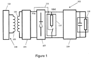
図1に示される典型的な非接触または誘導結合型(ICPT)システムは、送電器100及び受電器101を備える。送電器100は、磁界を生成するように電力送信(送電)コイル103を駆動するコントローラ102を備える。送信コイル103は、交流磁界を生成するように駆動されうる。受電器101は、電力受信(受電)コイル105、同調回路106、整流器107、負荷108、及び電力フロー制御回路109を備える。受信コイル105及び同調回路106は、共振回路を表現する。送電器100は、同調コンポーネントを有するかまたは有しない同様の共振回路を備える。
A typical contactless or inductively coupled (ICPT) system shown in FIG. 1 includes a
受信コイル105が送信コイル103にごく近接している場合、送電器100の磁界が受信コイル105内に電流を誘導する。磁界が交流であるため、誘導された交流電流は整流器107によって整流されて直流電流に変換され、それによりDC電力が負荷108へ送られる。これを実現するために、整流器107は、ハーフブリッジまたはフルブリッジの整流器であってもよいが、他の実装も可能である。更に、本発明には、AC電力を受電器側負荷へ送る実装を適用可能である。負荷108は、例えばコンシューマデバイスの充電可能バッテリーを表現してもよく、容量性素子及び抵抗素子を含むように描かれているが、これは例示にすぎず、より複雑な負荷でもよい。
When the
受信電力のレベルは、同調回路106によって受電器101の共振回路が共振させられる周波数に依存する。送電器及び受電器の共振回路の共振周波数のマッチングによって、最大電力伝送が可能になる。受電器側負荷へ送られる電力の制御は、様々な方法で提供される。例えば、送電器側の動作周波数を同調させるか、受電器側の共振周波数を同調させるか、またはその両方によって、制御が適用されうる。更に、負荷108への電力フロー制御は、負荷電力の要求条件を満たすように、負荷108へ送られる電力を調整する制御回路109によって提供される。例えば、制御回路109は、受電器負荷の要求条件に依存して、バック(Buck)、ブースト(boost)等のような構成を有する電力変換器であってもよい。
The level of the received power depends on the frequency at which the
従来、使用される電力フロー制御レジーム(regime)に関係なく、送電器側と受電器側とが結合されるとすぐに受電器側負荷へ直接、電力が送信されている。本発明は、受電器側回路内に予負荷回路を含めることで、上記の援用した米国仮出願番号61/722,564に記載の検出レジームの機能を拡張することによって、電力が受電器側へ送られる前に、送電器と受電器との間の互換性を確保する。 Conventionally, power is transmitted directly to the receiver-side load as soon as the transmitter and receiver are coupled, regardless of the power flow control regime used. The present invention extends the functionality of the detection regime described in the incorporated US provisional application Ser. No. 61 / 722,564 by including a preload circuit in the receiver-side circuit, whereby power is transferred to the receiver side. Before transmission, ensure compatibility between transmitter and receiver.
図1を再び参照すると、本発明のICPTシステムには、整流器107及び制御回路109によって提供される整流ステージと電力フロー制御ステージとの間に、予負荷回路110が更に設けられている。予負荷回路110は、ライン111を介して受信される送電器検出信号によって受電器側の共振回路内に誘導される非整流受信電力Pinを用いて操作されるスイッチング回路の制御下で、整流器107から出力される整流電圧Vintを受信するスイッチング可能負荷を表現する。予負荷回路110の目的は、固有の受電器検出信号を送電器に提供するように、送電器側検出信号によって提供されるエネルギーを、所定時間、シンクする(sink)ことである。以下では、予負荷回路のこの態様及び他の態様について、図2及び図3を参照して説明する。
Referring again to FIG. 1, the ICPT system of the present invention further includes a
図2は、例示的な予負荷回路210をブロック図として示し、図3は、予負荷回路210を例示的なフル回路図として示す。図2及び図3に示される予負荷回路の同様のエレメントには、同様の参照番号が付けられている。以下では、本発明の予負荷回路の構成及び例示的な動作について説明する。
FIG. 2 illustrates an
予負荷回路210は、整流電圧Vintを受信する予負荷211と、受電回路に対して予負荷211を接続/切断するための予負荷スイッチ212と、動作のための受信電力Pinをそれぞれ受信し、かつ、予負荷スイッチ212の動作のタイミング制御を一緒に提供する予負荷セット/リセット回路213及び予負荷切断回路214と、予負荷回路210をリセットするよう動作する予負荷リセットスイッチ215と、を有する。セット/リセット回路213とリセットスイッチ215との間のゲートスイッチ216、及び切断回路214と予負荷スイッチ212との間のゲートスイッチ217とが、更に設けられており、それらは予負荷電源218からの予備電力Pauxの制御下で動作する。
The
使用中には、送電器検出信号からの受信AC電力Pinが、予負荷回路210をアクティブ化するために入力される一方で、受電器101の整流ステージと調整ステージとの中間であるために本明細書で「中間電圧」と称される整流電圧Vintが、予負荷電源218をアクティブ化するために入力され、それにより予負荷スイッチ212及びリセットスイッチ215がオンになる。これは、予負荷211が、中間電圧Vintによって提供されるエネルギーを消散(dissipating)することでエネルギー「ダンプ(dump)」または電力「シンク(sink)」として動作することを可能にする。このエネルギーダンプは、送電器100へ逆に反射する急な電流突入を生じさせる。上記の援用した米国仮出願番号61/722,564に記載のように、このような反射突入信号は、受電器に対する結合を検出するために送電器によって使用される。しかし、これまでの受電器構成と異なり、本発明の受電器における予負荷回路の追加によって、受電器の結合の検出だけでなく、特定の受電器タイプの識別も可能になる。以下では、この識別について説明する。
In use, the received AC power Pin from the power transmitter detection signal is input to activate the
予負荷211は、中間電圧Vintに対するインピーダンスとして構成され、例えば図3において、予負荷211は抵抗素子を含むように描かれている。このため、種々の値の、及び/または種々の組み合わせで、抵抗、キャパシタ及び/またはインダクタで予負荷を構成することによって、予負荷211によって「ダンプされる」エネルギーの量が変化しうるとともに、その結果として、関連する反射突入信号の特性が変化しうる。したがって、固有に構成された予負荷回路を受電器に設けることで、特定の受電器を識別及び区別するために送電器によって使用可能な、受電器の固有の磁気信号または磁気シグネチャが提供される。これには多くの利点がある。
The
例えば、電力伝送を開始するための条件として、送電器によって送信された電力を本来的に受信できる受電器の結合にただ依存するのではなく、本発明のICPTシステムは、電力伝送前に送電器による受電器の検証を可能にする。この初期検証(またはハンドシェイク)は、個別にまたは種々の組み合わせで非網羅的に含む、以下の数々の理由で有利である。
1)安全性の増加:金属性の物体のような電気的に導電性の物体が送信コイルの近くにある場合に送信コイルには電力が供給されないことで、物体の望ましくない発熱を防がれ、その結果として、いわゆる異物検出(FOD:foreign object detection)の改善をもたらす。
2)ロバスト性の増加:互換性のない受電器に送電器によって電力が供給されることに起因する、受電器及び/または送電器の故障が防止される。
3)効率の増加:送電器の動作周波数が、検証された互換性のある受電器の共振周波数に対して動的かつ精密に同調されうる。
4)消費電力の減少:互換性のない受電器または異物が送電器の電力アップをトリガすることがないため、送電器は、互換性のある受電器が検出されるまで低電力スタンバイまたはスリープモードに維持されうる
5):互換性の増加:種々の互換性のある受電器を固有に識別する能力は、単一の送電器が多くの異なるタイプの受電器に電力供給するために使用可能となるように、例えば、ある範囲の電力レベルを送るように構成された送電器が、伝送の有効性を妥協することなく、7.5Wを要求するスマートフォンを充電するとともに15Wを要求するタブレットを充電するために使用可能となるように、適切な量の電力を送れることを意味する。
6)データ収集:送信コイルと受信コイルとの間のミスアライメントのような重要情報を集めることも可能である。
For example, rather than relying solely on coupling receivers that can inherently receive the power transmitted by the transmitter as a condition for initiating power transmission, the ICPT system of the present invention provides a means for transmitting power prior to power transmission. Enables verification of the receiver. This initial verification (or handshake) is advantageous for a number of reasons, including but not exhaustively individually or in various combinations.
1) Increased safety: when an electrically conductive object, such as a metallic object, is near the transmitting coil, no power is supplied to the transmitting coil, thereby preventing undesirable heating of the object. As a result, the so-called foreign object detection (FOD) is improved.
2) Increased robustness: Prevents failure of power receivers and / or power transmitters due to power supplied by power transmitters to incompatible power receivers.
3) Increased efficiency: the operating frequency of the transmitter can be dynamically and precisely tuned to the resonance frequency of a verified compatible receiver.
4) Reduced power consumption: the transmitter will remain in low power standby or sleep mode until a compatible receiver is detected, since incompatible receivers or foreign objects will not trigger the transmitter to power up. 5): Increased compatibility: The ability to uniquely identify various compatible power receivers allows a single transmitter to be used to power many different types of receivers. Thus, for example, a transmitter configured to send a range of power levels charges a smartphone that requires 7.5 W and a tablet that requires 15 W without compromising transmission effectiveness Means that an appropriate amount of power can be sent so that it can be used to
6) Data collection: It is also possible to collect important information such as misalignment between the transmitting and receiving coils.
本発明の予負荷回路210は、更に、広範囲の送電器‐受電器検出レジームをサポートするように構成される。即ち、受電器を検出するために、連続して素早く複数のエネルギーパルスを送信するように構成されうる。例えば、送電器は、エネルギーパルスを200マイクロ秒の長さで送信し、その後、最初のパルスと同じタイプ(周期及び周波数)であってもなくてもよい次のエネルギーパルスの感知前に、50マイクロ秒の期間、待機してもよい。予負荷回路210は、エネルギーパルスが受信されたら固有の磁気シグネチャが素早く通信されるとともに、後続のエネルギーパルスの受信前に当該回路に残っているあらゆるエネルギーを消散させるために当該回路が素早くリセットされるように、構成される。これは、予負荷スイッチ212及びリセットスイッチ215の動作によって達成され、それらのスイッチは、送電器エネルギーパルスの受信に応じて最初はオンにされ、その後、セット/リセット回路213及び切断回路214の動作によって設定される所定時間の後にオフにされる。当該所定時間は、予負荷回路210の切断及びリセットが、受電器の検出のために送電器によって送信される短周期エネルギーパルス間のタイミングまでに生じるように設定される。予負荷回路の切断は、後続するエネルギーパルス予負荷回路によってダンプされることを可能にするか、または、送電器からの通常の電力送信に応じて制御回路109を介した負荷108への通常の電力フローを可能にする。予負荷回路のセット及びリセットのタイミングは、後述するように達成される。
The
再び図3を参照して、以下では予負荷回路のフル回路例について説明する。セット/リセット回路213及び切断回路214のそれぞれは、電力変換器として構成された容量性素子及び抵抗素子を備え、それにより、入力AC電力Pinが、容量値及び抵抗値にそれぞれ依存する個別のDC信号へ変換される。ゲートスイッチ216,217は、半導体スイッチ、即ち、npn型のバイポーラ結合トランジスタとして構成され、ベースが、各DC信号を受信し、エミッタが、グランドに接続され、コレクタが、ゲートスイッチ216については予負荷リセットスイッチ215に接続され、ゲートスイッチ217については予負荷スイッチ212に接続されている。このように、セット/リセット回路213及び切断回路214からのDC信号が、ゲートスイッチ216,217を動作させる。
Referring to FIG. 3 again, a full circuit example of the preload circuit will be described below. Each of the set /
予負荷スイッチ212及び予負荷リセットスイッチ215も半導体スイッチとして構成されるが、n型の金属酸化膜半導体電界効果トランジスタ(nMOSFET)として構成され、ゲートが、プルアップ抵抗素子219,220をそれぞれ介して予負荷電源218からの予備電力Pauxを受信し、ソースが、グラウンド(図2も参照)に接続され、ドレインが、予負荷スイッチ212については予負荷211に接続され、予負荷リセットスイッチ215についてはゲートスイッチ217のベースに接続される。予負荷電源218は、容量性素子を備え、当該容量性素子は中間電圧Vintの受信に応じて充電され、それにより、予備電力Pauxを予負荷スイッチ212及び予負荷リセットスイッチ215のゲートへ供給して当該スイッチ212,215をデフォルトでオンにする。予負荷スイッチ212及び予負荷リセットスイッチ215の各ゲートは、ゲート‐ソース電圧が、nMOSFETに許容される最大定格を超えないことを確保にするために、それぞれのゲート電圧保護(ツェナー)ダイオード221,222にも接続される。
The
予負荷211によるエネルギー・ダンピングを停止するために、予負荷スイッチ212は、第1期間の後に、切断回路214によってオフにされる。予負荷回路210はその後リセットされる。当該リセットは、送電器100からの信号がセット/リセット回路213によって受信された際に予負荷リセットスイッチ215がまずオフにされ、その後、送電器100からの信号が停止した時点で予負荷リセットスイッチ215がオンにされることによって達成される。これは、第2期間を提供する。
To stop energy dumping by the
具体的には、AC電力Pinの受信は、セット/リセット回路213の容量性素子を充電させ、それにより、ゲートスイッチ216がオンになる。これは、予負荷リセットスイッチ215のトランジスタ・ゲートを、上述のデフォルトのハイ(high)状態からロー(low)にし、それにより予負荷リセットスイッチ215がオフになる。これは、第1及び第2期間の始まりを設定する。リセットスイッチ215がオフにされた時点で、切断回路214の容量性素子が充電され、それによりゲートスイッチ217がオンになる。これは、予負荷スイッチ212のトランジスタ・ゲートを、上述のデフォルトのハイ状態からローにし、それにより予負荷スイッチ212がオフになる。これは、第1期間の終わりを設定する。第1期間は、予負荷スイッチ212が短い時間オンを維持するように、ゲートスイッチ217がアクティブ化される前にAC電力Pinの受信から遅延を生じさせ、それにより、予負荷211が、固有の磁気シグネチャを作るために送電器エネルギーパルスからエネルギーをダンプすることが可能になる。
Specifically, reception of the AC power Pin causes the capacitive element of the set /
セット/リセット回路213及び切断回路214の相対的な構成は、予負荷リセットスイッチ215が素早くオフにされるとともに切断回路214内の電圧が上昇できるように、抵抗素子/容量素子の抵抗値/容量値を適切に選ぶことによって選択される。例えば、より大きいまたはより小さい抵抗値/容量値を有する抵抗素子及び/または容量性素子を選択することによって、切断回路214によって提供される第1期間の選択は、固有の異なる磁気シグネチャを作るように磁気シグネチャを変更する他の仕組みを提供する。
The relative configuration of the set /
AC電力が取り除かれた場合、即ち、送電器エネルギーパルスが停止した場合、セット/リセット回路213の容量性素子が放電し、それにより、予備電力Paux及びプルアップ抵抗素子220の影響下で、ゲートスイッチ216がオフになるとともに予負荷リセットスイッチ215のゲートが再びハイになる。その結果として、当該リセットスイッチ215がオンに戻り、それにより第2期間の終わりが設定される。これは、切断回路214に対する電圧をショートさせ、それにより、切断回路214の容量性素子が放電するとともに予負荷回路210がリセットされる。例えば抵抗素子/容量素子の抵抗値/容量値を適切に選ぶことによって、ゲートスイッチ216の動作のために可能性のある最小時間を設定するようにセット/リセット回路213を構成することで、切断回路214ができるだけ素早く放電されることが可能になる。したがって、予負荷回路210は、送電器からの後続するあらゆるエネルギーパルスに間に合うように、素早くリセットされる。
When the AC power is removed, ie, when the transmitter energy pulse stops, the capacitive element of the set /
図3に含まれる回路素子及びそのそれぞれの値が例示にすぎず、本発明のICPTシステムの動作及び利点を提供したまま他の構成及び/または値を選択できることを、当業者は理解する。同様に、本明細書に記載のあらゆる値も例示にすぎない。更に、本発明の予負荷回路は、ICPT受電器の、整流ステージと電力フロー制御ステージとの間の「中間」(または「整流された」)ステージに位置付けられるように記載されている。本発明のICPTシステムの動作及び利点を提供したまま、受電器内で予負荷回路について他の及び/または異なる位置を使用可能であることを、当業者は理解する。更には、本発明のICPTシステムの動作及び利点を提供したまま、送電器の検証のために送電器へ通信信号を送信するよう構成される場合には、受電器の代わりに、または受電器に加えて、送電器内に予負荷回路を位置付けることも可能である。 Those skilled in the art will understand that the circuit elements and their respective values included in FIG. 3 are merely exemplary, and that other configurations and / or values may be selected while still providing the operation and advantages of the ICPT system of the present invention. Similarly, any values set forth herein are merely exemplary. Further, the preload circuit of the present invention is described as being located at an "intermediate" (or "rectified") stage of the ICPT receiver between the rectification stage and the power flow control stage. One skilled in the art will appreciate that other and / or different locations for the preload circuit can be used in the receiver while still providing the operation and advantages of the ICPT system of the present invention. Furthermore, if it is configured to transmit a communication signal to a power transmitter for verification of the power transmitter while providing the operation and advantages of the ICPT system of the present invention, instead of the power receiver or to the power receiver. In addition, it is possible to locate the preload circuit in the power transmitter.
以下では、図4を参照して、図3の回路例との関連で予負荷回路の例示的な動作について説明する。本例では、送電器100によって受電器101へ送信される初期「ping」電力信号中で、受電器101が、図4の図(a)に示されるような送電器100からのAC電力を受信した場合、予負荷スイッチ212のゲートが十分な電圧となるまで(図4の図(b)のポイントB)、中間電圧Vintは急速に上昇する(図(c)領域A)。このポイントにおいて、予負荷211がグラウンドにショートされるため、予負荷スイッチ212は「オン」になって実質的に中間電圧の瞬時の急減が生じる(図4の図(c)のポイントC)。予負荷スイッチ212のゲートは一定期間(例えば、約200マイクロ秒から500マイクロ秒)、「ハイ」を維持し(図4の図(c)の期間ton)、その後、切断回路214によって「ロー」に切り替えられる(図4の図(b)のポイントD)。これは、中間電圧Vintを、受電器100の通常動作の典型レベルに戻させる(図4の図(c)のポイントE)。これは、予負荷スイッチ212のゲート電圧が「ロー」を維持し、かつ、予負荷スイッチ212がオフを維持する定常状態動作に、予負荷回路210が入るポイントである(図4の図(b)及び(c)のポイントF)。
In the following, with reference to FIG. 4, an exemplary operation of the preload circuit in connection with the example circuit of FIG. 3 will be described. In this example, in the initial “ping” power signal transmitted by
送電器100が電力の送信を停止した場合、受電器100(及び予負荷回路210)へのAC入力が停止する(図4の図(a)のポイントG)。これは、予負荷スイッチ212のゲート電圧を「ハイ」にプルさせる(図4の図(b)の領域H)。これにより、予負荷スイッチ212がオンになり、中間電圧が予負荷211を通じてグラウンドへショートされる(図4の図(c)の領域I)。受電器101に蓄積された全てのエネルギーは消散され、予負荷リセットスイッチ215の動作を介して予負荷回路210全体が素早く(約50マイクロ秒以内で)リセットされる(図4の図(b)の期間toffの後)。予負荷回路210は、送電器からの次のACパルスに応答できるようになる。
When the
本発明の実施形態の記述によって本発明を説明してきたが、また、実施形態を詳細に説明してきたが、添付の請求項の範囲を多少なりともそのような詳細に限定することは意図していない。更なる利点及び変更が、当業者には容易に見える。したがって、より広い態様の発明が、図示及び記述されている具体的な詳細、代表的な装置及び方法、並びに例示的な例に限定されることはない。このため、全体的な発明概念の精神または範囲から逸脱することなく、そのような詳細からの逸脱がなされてもよい。 Having described the invention with the description of the embodiments of the invention, and also described the embodiments in detail, it is intended that the scope of the appended claims be limited to such details in any way. Absent. Further advantages and modifications will be readily apparent to those skilled in the art. Accordingly, the invention in its broader aspects is not limited to the specific details, representative devices and methods, and illustrative examples shown and described. Thus, departures may be made from such details without departing from the spirit or scope of the general inventive concept.
Claims (7)
前記受電器は、前記電力パルスの受信に応じて固有の磁気信号を送信コイルへ反射する予負荷回路を備え、
前記受電器の前記予負荷回路は、1つ以上の抵抗器と、1つ以上のキャパシタと、スイッチング可能負荷と、スイッチとを備え、前記スイッチング可能負荷は、1つ以上の抵抗器の抵抗値及び1つ以上のキャパシタの容量値に依存するDC信号を使用して、スイッチングを生じて、前記磁気信号を提供するために、ある時間、前記受信された電力パルスによって前記受電器に生じる、ある量のエネルギーをシンクするように、構成されており、
前記1つ以上のキャパシタが、第1のキャパシタを有し、該第1のキャパシタが、前記ある時間に渡って前記電力パルスの受信の際に、充電して、前記ある時間の終りに前記スイッチのスイッチングを生じるDC信号を提供するように構成されている、ことを特徴とする受電器。 A power receiver for a non-contact power system, wherein the power receiver has a power receiving coil and is transmitted by the power transmitter via a non-contact electromagnetic coupling with a power transmission coil of the power transmitter. Configured to receive a power pulse;
The power receiver includes a preload circuit that reflects a unique magnetic signal to a transmission coil in response to receiving the power pulse,
The preload circuit of the power receiver includes one or more resistors, one or more capacitors, a switchable load, and a switch, wherein the switchable load has a resistance value of the one or more resistors. And using the DC signal that depends on the capacitance value of one or more capacitors to cause switching and provide the magnetic signal with the received power pulse at the receiver for a period of time. Is configured to sink an amount of energy,
The one or more capacitors include a first capacitor, the first capacitor charging upon receipt of the power pulse over the period of time, and switching the switch at the end of the period of time. A power receiver configured to provide a DC signal that causes switching of the power receiver.
前記電力パルスの受信に続く前記ある時間の始まりと、
前記電力パルスの受信に続く前記ある時間の終わりと、
のうちの1つ又は両方を設定するように構成された、抵抗器及びキャパシタを備えることを特徴とする請求項1に記載の受電器。 The one or more resistors and the one or more capacitors are:
Beginning of said certain time period following receipt of said power pulse;
At the end of the period of time following receipt of the power pulse;
One or configured to set both, resistors and the power receiver according to claim 1, characterized in that it comprises a capacitor of.
Applications Claiming Priority (5)
| Application Number | Priority Date | Filing Date | Title |
|---|---|---|---|
| NZ61760413 | 2013-11-11 | ||
| NZ617604 | 2013-11-11 | ||
| NZ628597 | 2014-08-12 | ||
| NZ62859714 | 2014-08-12 | ||
| PCT/NZ2014/000228 WO2015069121A1 (en) | 2013-11-11 | 2014-11-07 | Power receiver having magnetic signature and method for operating same |
Publications (3)
| Publication Number | Publication Date |
|---|---|
| JP2016536962A JP2016536962A (en) | 2016-11-24 |
| JP2016536962A5 JP2016536962A5 (en) | 2017-12-21 |
| JP6668238B2 true JP6668238B2 (en) | 2020-03-18 |
Family
ID=53041789
Family Applications (1)
| Application Number | Title | Priority Date | Filing Date |
|---|---|---|---|
| JP2016529995A Expired - Fee Related JP6668238B2 (en) | 2013-11-11 | 2014-11-07 | Power receiver having magnetic signature and method of operating the power receiver |
Country Status (6)
| Country | Link |
|---|---|
| US (1) | US10270280B2 (en) |
| EP (1) | EP3069452A4 (en) |
| JP (1) | JP6668238B2 (en) |
| KR (1) | KR102309240B1 (en) |
| CN (1) | CN105765874B (en) |
| WO (1) | WO2015069121A1 (en) |
Families Citing this family (2)
| Publication number | Priority date | Publication date | Assignee | Title |
|---|---|---|---|---|
| EP3544147A1 (en) * | 2018-03-20 | 2019-09-25 | Koninklijke Philips N.V. | Wireless power transfer system |
| DE102018120779B3 (en) | 2018-08-24 | 2019-12-12 | Phoenix Contact Gmbh & Co. Kg | Contactless PoE connection system |
Family Cites Families (14)
| Publication number | Priority date | Publication date | Assignee | Title |
|---|---|---|---|---|
| JP3392016B2 (en) * | 1996-09-13 | 2003-03-31 | 株式会社日立製作所 | Power transmission system and power transmission and information communication system |
| EP2266123B1 (en) | 2008-03-17 | 2018-10-10 | Powermat Technologies Ltd. | Inductive transmission system |
| JP4725611B2 (en) * | 2008-07-16 | 2011-07-13 | セイコーエプソン株式会社 | Power transmission control device, power transmission device, power reception control device, power reception device, and electronic device |
| US8712324B2 (en) * | 2008-09-26 | 2014-04-29 | Qualcomm Incorporated | Inductive signal transfer system for computing devices |
| US9130395B2 (en) * | 2008-12-12 | 2015-09-08 | Hanrim Postech Co., Ltd. | Non-contact charging station with planar spiral power transmission coil and method for controlling the same |
| JP5372537B2 (en) * | 2009-01-28 | 2013-12-18 | パナソニック株式会社 | Electronic device charging system, charger, and electronic device |
| JP5554937B2 (en) * | 2009-04-22 | 2014-07-23 | パナソニック株式会社 | Contactless power supply system |
| FI20095973A0 (en) * | 2009-09-22 | 2009-09-22 | Powerkiss Oy | Inductive power supply |
| JP5763675B2 (en) * | 2010-01-05 | 2015-08-12 | アクセス ビジネス グループ インターナショナル リミテッド ライアビリティ カンパニー | Inductive charging system for electric vehicles |
| JP2011229265A (en) | 2010-04-19 | 2011-11-10 | Panasonic Electric Works Co Ltd | Non-contacting power transmitter |
| JP5756925B2 (en) | 2011-05-19 | 2015-07-29 | パナソニックIpマネジメント株式会社 | Power receiving device provided in electrical equipment |
| US20120311363A1 (en) * | 2011-05-31 | 2012-12-06 | Nam Yun Kim | Wireless power transmission and charging system, and communication method of wireless power transmission and charging system |
| KR101811292B1 (en) * | 2011-07-06 | 2017-12-26 | 엘지전자 주식회사 | Wireless power transmitter and wireless power receiver having fuction of resonance frequency control |
| EP2915233A1 (en) | 2012-11-05 | 2015-09-09 | Powerbyproxi Limited | Inductively coupled power transfer systems |
-
2014
- 2014-11-07 EP EP14860279.0A patent/EP3069452A4/en not_active Withdrawn
- 2014-11-07 KR KR1020167015271A patent/KR102309240B1/en active IP Right Grant
- 2014-11-07 US US15/035,804 patent/US10270280B2/en active Active
- 2014-11-07 JP JP2016529995A patent/JP6668238B2/en not_active Expired - Fee Related
- 2014-11-07 WO PCT/NZ2014/000228 patent/WO2015069121A1/en active Application Filing
- 2014-11-07 CN CN201480061800.2A patent/CN105765874B/en active Active
Also Published As
| Publication number | Publication date |
|---|---|
| KR20160085827A (en) | 2016-07-18 |
| US20160301245A1 (en) | 2016-10-13 |
| US10270280B2 (en) | 2019-04-23 |
| CN105765874B (en) | 2021-10-22 |
| CN105765874A (en) | 2016-07-13 |
| JP2016536962A (en) | 2016-11-24 |
| EP3069452A4 (en) | 2017-07-12 |
| EP3069452A1 (en) | 2016-09-21 |
| WO2015069121A1 (en) | 2015-05-14 |
| KR102309240B1 (en) | 2021-10-06 |
Similar Documents
| Publication | Publication Date | Title |
|---|---|---|
| US10270277B2 (en) | System and method for prevention of wireless charging cross connection | |
| US7565204B2 (en) | Implantable device for controlling received power by a power receiving unit therein | |
| US10069346B2 (en) | Wireless power receiver and control method thereof | |
| US20220224161A1 (en) | Wireless charging device, a receiver device, and a method of operating the same | |
| JP5901636B2 (en) | Overvoltage protection for AC power supply | |
| KR101987315B1 (en) | Wireless power transfer device and energy charging device | |
| JPWO2017145602A1 (en) | Wireless power transmission apparatus, control method therefor, power transmission control circuit, charger | |
| KR20140090669A (en) | A method for controlling a converter | |
| JP6668238B2 (en) | Power receiver having magnetic signature and method of operating the power receiver | |
| WO2013015208A1 (en) | Device with built-in battery, and charging station and device with built-in battery | |
| CN109756006B (en) | System and method for electric vehicle wireless charger output protection | |
| KR20160142524A (en) | Wireless charging device | |
| JP2007336787A (en) | Contactless power supply system, power supply device, and power receiving device | |
| KR101999520B1 (en) | Integrated system of wireless power charging and short distance wireless communication and integrated controller for the same | |
| US10705130B2 (en) | Adaptive transmitter present detection | |
| JP2018046637A (en) | Wireless power supply system | |
| Huang et al. | A wireless power transfer system with enhanced response and efficiency by fully-integrated fast-tracking wireless constant-idle-time control for implants | |
| KR20220008916A (en) | Wireless power transmitter with multiple primary and adjacent coil muting capabilities | |
| KR20160144124A (en) | Gateway for internet of things | |
| CN108123429A (en) | Excess voltage protection | |
| Ansah | Design and Implementation of a GSM Based Wireless Power Transfer for AC or DC Load | |
| CN108123422A (en) | Excess voltage protection | |
| WO2016097476A1 (en) | Switched-mode power supply |
Legal Events
| Date | Code | Title | Description |
|---|---|---|---|
| A521 | Request for written amendment filed |
Free format text: JAPANESE INTERMEDIATE CODE: A523 Effective date: 20171106 |
|
| A621 | Written request for application examination |
Free format text: JAPANESE INTERMEDIATE CODE: A621 Effective date: 20171106 |
|
| A711 | Notification of change in applicant |
Free format text: JAPANESE INTERMEDIATE CODE: A711 Effective date: 20180227 |
|
| A131 | Notification of reasons for refusal |
Free format text: JAPANESE INTERMEDIATE CODE: A131 Effective date: 20180827 |
|
| A521 | Request for written amendment filed |
Free format text: JAPANESE INTERMEDIATE CODE: A523 Effective date: 20181126 |
|
| A131 | Notification of reasons for refusal |
Free format text: JAPANESE INTERMEDIATE CODE: A131 Effective date: 20190401 |
|
| A521 | Request for written amendment filed |
Free format text: JAPANESE INTERMEDIATE CODE: A523 Effective date: 20190624 |
|
| A02 | Decision of refusal |
Free format text: JAPANESE INTERMEDIATE CODE: A02 Effective date: 20191007 |
|
| A521 | Request for written amendment filed |
Free format text: JAPANESE INTERMEDIATE CODE: A523 Effective date: 20200116 |
|
| A911 | Transfer to examiner for re-examination before appeal (zenchi) |
Free format text: JAPANESE INTERMEDIATE CODE: A911 Effective date: 20200124 |
|
| TRDD | Decision of grant or rejection written | ||
| A01 | Written decision to grant a patent or to grant a registration (utility model) |
Free format text: JAPANESE INTERMEDIATE CODE: A01 Effective date: 20200210 |
|
| A61 | First payment of annual fees (during grant procedure) |
Free format text: JAPANESE INTERMEDIATE CODE: A61 Effective date: 20200226 |
|
| R150 | Certificate of patent or registration of utility model |
Ref document number: 6668238 Country of ref document: JP Free format text: JAPANESE INTERMEDIATE CODE: R150 |
|
| LAPS | Cancellation because of no payment of annual fees |