JP6500845B2 - Method of manufacturing bonded wafer - Google Patents
Method of manufacturing bonded wafer Download PDFInfo
- Publication number
- JP6500845B2 JP6500845B2 JP2016118094A JP2016118094A JP6500845B2 JP 6500845 B2 JP6500845 B2 JP 6500845B2 JP 2016118094 A JP2016118094 A JP 2016118094A JP 2016118094 A JP2016118094 A JP 2016118094A JP 6500845 B2 JP6500845 B2 JP 6500845B2
- Authority
- JP
- Japan
- Prior art keywords
- wafer
- temperature
- heat treatment
- bonded
- peeling
- Prior art date
- Legal status (The legal status is an assumption and is not a legal conclusion. Google has not performed a legal analysis and makes no representation as to the accuracy of the status listed.)
- Active
Links
- 238000004519 manufacturing process Methods 0.000 title claims description 28
- 238000010438 heat treatment Methods 0.000 claims description 112
- 238000000034 method Methods 0.000 claims description 15
- 150000002500 ions Chemical class 0.000 claims description 12
- 238000005468 ion implantation Methods 0.000 claims description 10
- 239000007789 gas Substances 0.000 claims description 9
- XLYOFNOQVPJJNP-UHFFFAOYSA-N water Substances O XLYOFNOQVPJJNP-UHFFFAOYSA-N 0.000 claims description 9
- XUIMIQQOPSSXEZ-UHFFFAOYSA-N Silicon Chemical compound [Si] XUIMIQQOPSSXEZ-UHFFFAOYSA-N 0.000 claims description 8
- 239000001257 hydrogen Substances 0.000 claims description 8
- 229910052739 hydrogen Inorganic materials 0.000 claims description 8
- 229910052710 silicon Inorganic materials 0.000 claims description 8
- 239000010703 silicon Substances 0.000 claims description 8
- -1 hydrogen ions Chemical class 0.000 claims description 6
- 238000012545 processing Methods 0.000 claims description 6
- 239000013078 crystal Substances 0.000 claims description 4
- 235000012431 wafers Nutrition 0.000 description 160
- 230000003746 surface roughness Effects 0.000 description 35
- 239000010408 film Substances 0.000 description 21
- 230000003647 oxidation Effects 0.000 description 8
- 238000007254 oxidation reaction Methods 0.000 description 8
- 238000005498 polishing Methods 0.000 description 8
- 239000010409 thin film Substances 0.000 description 7
- 238000004140 cleaning Methods 0.000 description 5
- 230000000052 comparative effect Effects 0.000 description 5
- UFHFLCQGNIYNRP-UHFFFAOYSA-N Hydrogen Chemical compound [H][H] UFHFLCQGNIYNRP-UHFFFAOYSA-N 0.000 description 3
- 238000002513 implantation Methods 0.000 description 3
- 238000000137 annealing Methods 0.000 description 2
- 230000007547 defect Effects 0.000 description 2
- 238000009792 diffusion process Methods 0.000 description 2
- 230000000694 effects Effects 0.000 description 2
- 239000011261 inert gas Substances 0.000 description 2
- 230000001590 oxidative effect Effects 0.000 description 2
- 239000002245 particle Substances 0.000 description 2
- VHUUQVKOLVNVRT-UHFFFAOYSA-N Ammonium hydroxide Chemical compound [NH4+].[OH-] VHUUQVKOLVNVRT-UHFFFAOYSA-N 0.000 description 1
- 235000011114 ammonium hydroxide Nutrition 0.000 description 1
- QVGXLLKOCUKJST-UHFFFAOYSA-N atomic oxygen Chemical compound [O] QVGXLLKOCUKJST-UHFFFAOYSA-N 0.000 description 1
- 238000003776 cleavage reaction Methods 0.000 description 1
- 238000007796 conventional method Methods 0.000 description 1
- 238000001816 cooling Methods 0.000 description 1
- 238000009826 distribution Methods 0.000 description 1
- 238000005538 encapsulation Methods 0.000 description 1
- 238000005516 engineering process Methods 0.000 description 1
- 230000002708 enhancing effect Effects 0.000 description 1
- 150000002431 hydrogen Chemical class 0.000 description 1
- QOSATHPSBFQAML-UHFFFAOYSA-N hydrogen peroxide;hydrate Chemical compound O.OO QOSATHPSBFQAML-UHFFFAOYSA-N 0.000 description 1
- 239000007943 implant Substances 0.000 description 1
- 238000003754 machining Methods 0.000 description 1
- 238000012423 maintenance Methods 0.000 description 1
- 238000005259 measurement Methods 0.000 description 1
- 238000013508 migration Methods 0.000 description 1
- 230000005012 migration Effects 0.000 description 1
- 239000011259 mixed solution Substances 0.000 description 1
- 239000001301 oxygen Substances 0.000 description 1
- 229910052760 oxygen Inorganic materials 0.000 description 1
- 238000009832 plasma treatment Methods 0.000 description 1
- 229910052761 rare earth metal Inorganic materials 0.000 description 1
- 230000000630 rising effect Effects 0.000 description 1
- 230000007017 scission Effects 0.000 description 1
- 238000000926 separation method Methods 0.000 description 1
- 239000000243 solution Substances 0.000 description 1
- 239000011800 void material Substances 0.000 description 1
Images

Classifications
-
- H—ELECTRICITY
- H01—ELECTRIC ELEMENTS
- H01L—SEMICONDUCTOR DEVICES NOT COVERED BY CLASS H10
- H01L21/00—Processes or apparatus adapted for the manufacture or treatment of semiconductor or solid state devices or of parts thereof
- H01L21/02—Manufacture or treatment of semiconductor devices or of parts thereof
- H01L21/04—Manufacture or treatment of semiconductor devices or of parts thereof the devices having at least one potential-jump barrier or surface barrier, e.g. PN junction, depletion layer or carrier concentration layer
- H01L21/18—Manufacture or treatment of semiconductor devices or of parts thereof the devices having at least one potential-jump barrier or surface barrier, e.g. PN junction, depletion layer or carrier concentration layer the devices having semiconductor bodies comprising elements of Group IV of the Periodic System or AIIIBV compounds with or without impurities, e.g. doping materials
- H01L21/26—Bombardment with radiation
- H01L21/263—Bombardment with radiation with high-energy radiation
- H01L21/265—Bombardment with radiation with high-energy radiation producing ion implantation
-
- H—ELECTRICITY
- H01—ELECTRIC ELEMENTS
- H01L—SEMICONDUCTOR DEVICES NOT COVERED BY CLASS H10
- H01L27/00—Devices consisting of a plurality of semiconductor or other solid-state components formed in or on a common substrate
- H01L27/02—Devices consisting of a plurality of semiconductor or other solid-state components formed in or on a common substrate including semiconductor components specially adapted for rectifying, oscillating, amplifying or switching and having at least one potential-jump barrier or surface barrier; including integrated passive circuit elements with at least one potential-jump barrier or surface barrier
- H01L27/12—Devices consisting of a plurality of semiconductor or other solid-state components formed in or on a common substrate including semiconductor components specially adapted for rectifying, oscillating, amplifying or switching and having at least one potential-jump barrier or surface barrier; including integrated passive circuit elements with at least one potential-jump barrier or surface barrier the substrate being other than a semiconductor body, e.g. an insulating body
Description
本発明は、貼り合わせウェーハの製造方法に関する。 The present invention relates to a method of manufacturing a bonded wafer.
近年、貼り合わせウェーハの製造方法として、イオン注入したウェーハを他のウェーハと接合して剥離することで貼り合わせウェーハを製造する方法(イオン注入剥離法:スマートカット法(登録商標)とも呼ばれる技術)が新たに注目され始めている。 In recent years, as a method of manufacturing bonded wafers, a method of manufacturing bonded wafers by bonding and peeling an ion-implanted wafer with another wafer (ion-implant peeling method: technology also referred to as smart cut method (registered trademark)) Is beginning to attract new attention.
このようなイオン注入剥離法によりSOIウェーハを製造する方法としては、2枚のシリコンウェーハのうち、少なくとも一方に酸化膜を形成するとともに、一方のシリコンウェーハ(ボンドウェーハ)の上面から水素イオンや希ガスイオン等のガスイオンを注入し、該ボンドウェーハ内部に微小気泡層(封入層)を形成させる。そして、イオン注入した側の面を酸化膜を介して他方のシリコンウェーハ(ベースウェーハ)と密着させ、その後熱処理(剥離熱処理)を加えて微小気泡層を劈開面として一方のウェーハ(ボンドウェーハ)を薄膜状に剥離し、さらに熱処理(結合熱処理)を加えて強固に結合してSOIウェーハとする(特許文献1参照)。この方法では、劈開面(剥離面)が良好な鏡面で、膜厚の均一性が高いSOI層を有するSOIウェーハが比較的容易に得られる。 As a method of manufacturing an SOI wafer by such an ion implantation peeling method, an oxide film is formed on at least one of two silicon wafers, and hydrogen ions or a rare earth ion are generated from the upper surface of one silicon wafer (bond wafer). Gas ions such as gas ions are implanted to form a microbubble layer (encapsulation layer) inside the bond wafer. Then, the surface on the ion-implanted side is brought into close contact with the other silicon wafer (base wafer) through the oxide film, and then heat treatment (peeling heat treatment) is applied to make one wafer (bond wafer) A thin film is peeled off, and a heat treatment (bonding heat treatment) is further added to bond firmly to form an SOI wafer (see Patent Document 1). In this method, an SOI wafer having an SOI layer with a mirror surface with a good cleavage surface (peeling surface) and a high uniformity of film thickness can be obtained relatively easily.
しかし、イオン注入剥離法により貼り合わせウェーハを作製する場合においては、剥離後の貼り合わせウェーハ表面にイオン注入によるダメージ層が存在し、また通常の製品レベルのシリコンウェーハの鏡面に比べて表面粗さが大きなものとなる。従って、イオン注入剥離法による製造では、このようなダメージ層及び表面粗さを除去することが必要になる。 However, in the case of producing a bonded wafer by the ion implantation peeling method, a damaged layer due to ion implantation exists on the bonded wafer surface after peeling, and the surface roughness as compared to the mirror surface of a normal product level silicon wafer. Is a big thing. Therefore, in the manufacture by the ion implantation peeling method, it is necessary to remove such a damage layer and surface roughness.
従来、このダメージ層等を除去するために、結合熱処理後の最終工程において、タッチポリッシュと呼ばれる研磨代の極めて少ない鏡面研磨(取り代:100nm程度)が行われていた。 Conventionally, in order to remove the damaged layer and the like, mirror polishing (removal: about 100 nm) with a very small amount of polishing allowance called touch polishing has been performed in the final step after the bonding heat treatment.
ところが、貼り合わせウェーハの薄膜(SOI層)に機械加工的要素を含む研磨を施すと、研磨の取り代が面内で均一でないために、水素イオン等の注入、剥離によって達成された薄膜の膜厚均一性が悪化してしまうという問題が生じる。 However, when the thin film (SOI layer) of the bonded wafer is subjected to polishing including a machining element, the film of the thin film achieved by implanting and peeling of hydrogen ions or the like because the removal of polishing is not uniform in the plane. There is a problem that the thickness uniformity is deteriorated.
このような問題点を解決する方法として、前記タッチポリッシュの代わりに高温熱処理を行って表面粗さを改善する平坦化熱処理が行われるようになってきている。 As a method of solving such problems, a flattening heat treatment has been performed to improve the surface roughness by performing a high temperature heat treatment instead of the touch polishing.
特に、特許文献2では、表面粗さの短周期粗さと長周期粗さに注目し、平坦化熱処理において、急速加熱・急速冷却装置(RTA装置)とヒータ加熱式熱処理炉(バッチ式炉)による2段階の熱処理を行うことによって、表面粗さの短周期粗さと長周期粗さの両者を低減する方法が提案されている。
In particular,
また、特許文献3では、剥離面を直接酸化する際に発生しやすいOSF(酸化誘起積層欠陥)を回避するため、不活性ガス、水素ガス、あるいはこれらの混合ガス雰囲気下での平坦化熱処理の後に犠牲酸化処理を行うことにより、剥離面の平坦化とOSFの回避を同時に達成している。また、犠牲酸化の前に70nm以下の取り代の研磨を実施することで、表面粗さの長周期成分を一層低減することを提案している。
Further, in
また、特許文献4では、剥離後の貼り合わせウェーハの結合強度を高めるための結合熱処理を酸化性雰囲気で行う際、剥離面に発生しやすいOSFを確実に回避するため、結合熱処理として、950℃未満の温度で酸化熱処理を行った後に、5%以下の酸素を含む不活性ガス雰囲気で、1000℃以上の温度で熱処理を行うことが開示されている。 Further, in Patent Document 4, when performing bonding heat treatment for enhancing the bonding strength of the bonded wafer after peeling in an oxidizing atmosphere, 950 ° C. is used as the bonding heat treatment in order to reliably avoid OSF that tends to occur on the peeling surface. It is disclosed that the heat treatment is performed at a temperature of 1000 ° C. or more in an inert gas atmosphere containing 5% or less of oxygen after the oxidation heat treatment is performed at a temperature lower than that.
剥離面の平坦化処理として研磨を行うことなく高温の熱処理のみを行う場合、熱処理温度が高い方が平坦度を高めることができる。特許文献2によれば、短周期成分を改善するためのRTA装置による熱処理温度としては、1200〜1350℃の温度範囲とするのがより効果的であるとしており、また、長周期成分を改善するためのバッチ式炉による熱処理温度としても同様に、1200〜1350℃の温度範囲とするのがより効果的であるとしている。そして、実施例においては、いずれの熱処理も1200℃以上の熱処理が行われている。また、特許文献3でも同様に、平坦化熱処理のArアニールとして、1200℃の熱処理温度のみが開示されている。
When only heat treatment at high temperature is performed without polishing as planarization treatment of the peeled surface, the flatness can be increased as the heat treatment temperature is higher. According to
これらの記載からも明らかなように、熱処理のみの平坦化処理でデバイスプロセスに十分に適用できる表面粗さを得るためには、1200℃以上の熱処理温度が必要であるとされており、実際の量産でも1200℃以上の温度が採用されていた。 As apparent from these descriptions, in order to obtain surface roughness that can be sufficiently applied to a device process by planarization treatment of only heat treatment, a heat treatment temperature of 1200 ° C. or more is considered to be necessary, and Even in mass production, temperatures of 1200 ° C. or higher were adopted.
しかしながら、1200℃以上の温度で熱処理を行うとスリップ転位が発生する確率が高まるため、製品歩留まりの低下をもたらし、結果として製造コストの増加を招いていた。 However, when the heat treatment is performed at a temperature of 1200 ° C. or higher, the probability of occurrence of slip dislocations is increased, which results in a decrease in product yield, resulting in an increase in manufacturing cost.
そこで、剥離熱処理後の剥離面の表面粗さを小さくできれば、その後の工程で、表面粗さを低減させるための平坦化熱処理に負荷をかけないように処理できる。 Therefore, if the surface roughness of the peeling surface after the peeling heat treatment can be made smaller, it can be treated so as not to load the flattening heat treatment for reducing the surface roughness in the subsequent steps.
例えばArアニールによるマイグレーションを利用する場合、剥離面の表面粗さの小さな貼り合わせウェーハは低温で処理することが可能となり、スリップ転位の発生は少なくなり、パーティクルの増加も少なくなる。しかし、剥離面の表面粗さの大きな貼り合わせウェーハでは、表面粗さを小さくするため、より高温での処理が必要となる。従って、スリップ、パーティクル等の対策が必要となる。また、剥離熱処理後の剥離面の表面粗さが大きい場合、その貼り合わせウェーハの剥離起因の欠陥が多く存在し、その欠陥を消滅させるためより厚い酸化膜厚の犠牲酸化が必要となる。 For example, when migration by Ar annealing is used, a bonded wafer having a small surface roughness of the separation surface can be processed at a low temperature, the occurrence of slip dislocations is reduced, and the increase of particles is also reduced. However, in the case of a bonded wafer having a large surface roughness of the peeling surface, treatment at a higher temperature is required to reduce the surface roughness. Therefore, measures such as slip and particles are required. Further, when the surface roughness of the peeling surface after the peeling heat treatment is large, many defects caused by peeling of the bonded wafer exist, and in order to eliminate the defects, sacrificial oxidation of a thicker oxide film thickness is required.
本発明は、上記事情に鑑みなされたもので、例えばSOIウェーハのような貼り合わせウェーハの剥離後の剥離面の表面粗さを低減させることで、より低い温度での平坦化熱処理により最終的な貼り合わせウェーハの表面の表面粗さを低下させることができる貼り合わせウェーハの製造方法を提供することを目的とする。 The present invention has been made in view of the above-mentioned circumstances, and for example, by reducing the surface roughness of the peeling surface after peeling of a bonded wafer such as an SOI wafer, the final heat treatment is performed by flattening heat treatment at a lower temperature. An object of the present invention is to provide a method for producing a bonded wafer which can reduce the surface roughness of the surface of the bonded wafer.
上記課題を解決するために、本発明では、シリコン単結晶ウェーハからなるボンドウェーハの表面から水素イオン、希ガスイオンの少なくとも一種類のガスイオンをイオン注入して前記ボンドウェーハの内部にイオン注入層を形成し、前記ボンドウェーハのイオン注入した表面とベースウェーハの表面とを直接又は絶縁膜を介して貼り合わせた後、剥離熱処理を行うことによって前記イオン注入層で前記ボンドウェーハを剥離させて貼り合わせウェーハを製造する貼り合わせウェーハの製造方法において、前記ボンドウェーハと前記ベースウェーハとを貼り合わせた後、前記剥離熱処理を行うまで、貼り合わせた前記ボンドウェーハと前記ベースウェーハとの貼り合わせ界面が水分子の寄与によって結合している状態で前記貼り合わせたボンドウェーハとベースウェーハを室温で12時間以上保持し、前記剥離熱処理は、炉内温度が400℃以上500℃以下の一定温度に設定された熱処理炉内に前記貼り合わせたボンドウェーハとベースウェーハを昇温工程なしで直接投入し、前記一定温度で熱処理するか、又は、前記一定温度から+50℃以内の所定温度に昇温したのち該所定温度で熱処理する貼り合わせウェーハの製造方法を提供する。 In order to solve the above problems, in the present invention, at least one kind of gas ions of hydrogen ions and rare gas ions are implanted from the surface of a bond wafer made of a silicon single crystal wafer, and the ion implanted layer is formed inside the bond wafer. And bonding the ion-implanted surface of the bond wafer and the surface of the base wafer directly or through an insulating film, and then performing a peeling heat treatment to peel and bond the bond wafer with the ion-implanted layer. In a method of manufacturing a bonded wafer for manufacturing a laminated wafer, after bonding the bond wafer and the base wafer, a bonding interface between the bonded wafer and the base wafer is bonded until the peeling heat treatment is performed. The bonded bon in the bound state by the contribution of water molecules The wafer and the base wafer are held at room temperature for 12 hours or more, and the peeling heat treatment is performed by raising the bonded wafer and the base wafer in a heat treatment furnace in which the temperature in the furnace is set to a constant temperature of 400 ° C. to 500 ° C. There is provided a method for producing a bonded wafer which is directly charged without a heating step, heat-treated at the constant temperature, or heated to a predetermined temperature within + 50 ° C. from the constant temperature and heat-treated at the predetermined temperature.
このような貼り合わせウェーハの製造方法であれば、例えばSOIウェーハのような貼り合わせウェーハの剥離後の剥離面の表面粗さを低減させることができるので、より低い温度での平坦化熱処理により最終的な貼り合わせウェーハの表面(SOI層の表面)の表面粗さを低下させることができる。また、貼り合わせたウェーハを室温で12時間以上保持することによって、熱処理炉に投入する際のボンドウェーハとベースウェーハとの貼り合わせ強度を高めておくことができ、これによりボイドの発生を抑制できる。 If it is a manufacturing method of such a bonded wafer, for example, the surface roughness of the peeling surface after peeling of the bonded wafer such as an SOI wafer can be reduced, so that the final treatment is performed by the flattening heat treatment at a lower temperature. Surface roughness of the surface of the bonded wafer (surface of the SOI layer) can be reduced. Further, by holding the bonded wafer at room temperature for 12 hours or more, the bonding strength between the bond wafer and the base wafer at the time of being introduced into the heat treatment furnace can be enhanced, thereby suppressing the generation of voids. .
このとき、前記一定温度又は前記所定温度で熱処理した後に、前記熱処理炉から前記貼り合わせウェーハを取り出す際の温度を、前記剥離熱処理の際の温度と同一温度とすることが好ましい。 At this time, it is preferable that the temperature at the time of taking out the bonded wafer from the heat treatment furnace after heat treatment at the constant temperature or the predetermined temperature be the same temperature as the temperature in the peeling heat treatment.
熱処理炉から貼り合わせウェーハを取り出す際の温度を、剥離熱処理の際の温度と同一温度とすれば、降温工程を省略することができるので効率的であり、製造コストを低減させることができる。 If the temperature at the time of taking out the bonded wafer from the heat treatment furnace is the same temperature as the temperature at the peeling heat treatment, the temperature lowering step can be omitted, which is efficient and can reduce the manufacturing cost.
またこのとき、前記室温で保持する時間を48時間以上とすることが好ましい。 At this time, it is preferable to set the holding time at room temperature to 48 hours or more.
このようにすれば、ボンドウェーハとベースウェーハとの貼り合わせ強度をより一層高めることができる。 By so doing, the bonding strength between the bond wafer and the base wafer can be further enhanced.
またこのとき、前記剥離熱処理の後に、前記ボンドウェーハを剥離した貼り合わせウェーハの剥離面を平坦化する熱処理を行い、該平坦化する熱処理の温度を1100℃〜1175℃の温度範囲内で行うことが好ましい。 At this time, after the peeling heat treatment, a heat treatment for flattening the peeling surface of the bonded wafer from which the bond wafer is peeled is performed, and the temperature of the heat treatment for flattening is performed within a temperature range of 1100 ° C to 1175 ° C. Is preferred.
このような温度範囲で平坦化熱処理を行えば、スリップ転位が発生する確率が低下するため、製品歩留まりが向上し、結果として製造コストを低下させることができる。 If the planarization heat treatment is performed in such a temperature range, the probability of the occurrence of slip dislocation is reduced, so that the product yield can be improved, and as a result, the manufacturing cost can be reduced.
またこのとき、前記ボンドウェーハと前記ベースウェーハとを貼り合わせる前に、前記ボンドウェーハ及び前記ベースウェーハを洗浄することが好ましい。 At this time, it is preferable to clean the bond wafer and the base wafer before bonding the bond wafer and the base wafer.
このように、本発明では、ボンドウェーハとベースウェーハとを貼り合わせる前に、ボンドウェーハ及びベースウェーハを洗浄することで、ボンドウェーハ及びベースウェーハの表面に水分子を十分に残すことができ、また、ボンドウェーハとベースウェーハとを貼り合わせた際に、貼り合わせたウェーハの貼り合わせ界面が水分子の寄与によって結合している状態とすることができる。 As described above, according to the present invention, by cleaning the bond wafer and the base wafer before bonding the bond wafer and the base wafer, sufficient water molecules can be left on the surfaces of the bond wafer and the base wafer. When bonding the bond wafer and the base wafer, the bonded interface of the bonded wafers can be in a state of being bonded by the contribution of water molecules.
本発明の貼り合わせウェーハの製造方法であれば、例えばSOIウェーハのような貼り合わせウェーハの剥離後の剥離面の表面粗さを低減させることができるので、より低い温度での平坦化熱処理により最終的な貼り合わせウェーハの表面(SOI層の表面)の表面粗さを低下させることができる。また、貼り合わせたウェーハを室温で12時間以上保持することによって、熱処理炉に投入する際のボンドウェーハとベースウェーハとの貼り合わせ強度を高めておくことができ、これによりボイドの発生を抑制できる。 With the method for producing a bonded wafer according to the present invention, for example, the surface roughness of the peeling surface after peeling of a bonded wafer such as an SOI wafer can be reduced, so the final treatment by planarization heat treatment at a lower temperature Surface roughness of the surface of the bonded wafer (surface of the SOI layer) can be reduced. Further, by holding the bonded wafer at room temperature for 12 hours or more, the bonding strength between the bond wafer and the base wafer at the time of being introduced into the heat treatment furnace can be enhanced, thereby suppressing the generation of voids. .
以下、本発明について、より具体的に説明する。
上述のように、例えばSOIウェーハあるいは絶縁膜を介さないダイレクトボンドウェーハのような貼り合わせウェーハの剥離後の剥離面の表面粗さを低減させることで、より低い温度での平坦化熱処理により最終的な貼り合わせウェーハの表面(SOI層の表面)の表面粗さを低下させることができる貼り合わせウェーハの製造方法が求められていた。
Hereinafter, the present invention will be described more specifically.
As described above, for example, by reducing the surface roughness of the peeling surface after peeling of a bonded wafer such as an SOI wafer or a direct bond wafer not via an insulating film, the final heat treatment is performed by planarization heat treatment at a lower temperature. There has been a demand for a method for producing a bonded wafer which can reduce the surface roughness of the surface of the bonded wafer (the surface of the SOI layer).
通常、イオン注入剥離法で剥離熱処理を行う際には、例えば特開2003−347526号等に記載されているように、350℃程度の低温に保持された熱処理炉に貼り合わせたウェーハを投入して一定時間保持した後、500℃以上の温度に昇温して所定時間保持する方法が行われる。しかしながら、このような熱処理を行うと、剥離が生じる500℃に達するまでの間に、イオン注入された水素の拡散がわずかながら進行し、注入層の水素濃度分布が広がってしまう。その状態で剥離が生じると、剥離領域の幅(深さ方向の幅)が広くなり、結果として剥離面の表面粗さは大きくなる。 Usually, when performing the peeling heat treatment by the ion implantation peeling method, for example, as described in JP-A 2003-347526 etc., the bonded wafer is put into a heat treatment furnace maintained at a low temperature of about 350 ° C. After holding for a predetermined time, the temperature is raised to 500 ° C. or higher and held for a predetermined time. However, when such a heat treatment is performed, diffusion of ion-implanted hydrogen progresses slightly while reaching the temperature of 500 ° C. where peeling occurs, and the hydrogen concentration distribution of the implanted layer is broadened. If peeling occurs in that state, the width of the peeled area (the width in the depth direction) widens, and as a result, the surface roughness of the peeled surface increases.
そこで、本発明者らは、水素の拡散を抑えるために、剥離が可能な温度に、昇温工程なしで直接投入するか、又は、一定温度から+50℃以内の所定温度に昇温したのちこの所定温度で熱処理することにより、剥離後の剥離面の表面粗さを低減することができることを見出した。ただし、このように従来よりも高温で熱処理炉に投入する場合、投入時の結合力が弱いと完全な剥離が得られずに、ボイドの発生を伴ってしまう。本発明者らは、その対策として、ボンドウェーハとベースウェーハとを貼り合わせた後、剥離熱処理を行うまで、貼り合わせ界面が水分子の寄与によって結合している状態で貼り合わせたウェーハを室温で長時間保持することによって、熱処理炉に投入する際のボンドウェーハとベースウェーハとの貼り合わせ強度を高めておくことにより、上記課題を解決できることを見出し、本発明を完成させた。 Therefore, in order to suppress the diffusion of hydrogen, the present inventors directly charge the temperature at which peeling is possible without a temperature raising step, or raise the temperature from a certain temperature to a predetermined temperature within + 50 ° C. It has been found that the surface roughness of the peeled surface after peeling can be reduced by heat treatment at a predetermined temperature. However, when the heat treatment furnace is charged at a temperature higher than that of the prior art as described above, if the bond strength at the time of the charge is weak, complete peeling can not be obtained, and a void is accompanied. As a countermeasure, after bonding a bond wafer and a base wafer as the countermeasure, until a peeling heat treatment is performed, the bonded wafer is bonded at a room temperature with the bonding interface bonded by the contribution of water molecules. By maintaining the bonding strength between the bond wafer and the base wafer at the time of being put into the heat treatment furnace by holding for a long time, it is found that the above problem can be solved, and the present invention has been completed.
以下、本発明について、図面を参照しながら詳細に説明するが、本発明はこれらに限定されるものではない。 Hereinafter, the present invention will be described in detail with reference to the drawings, but the present invention is not limited thereto.
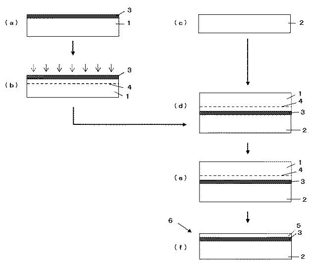
図1は、本発明の貼り合わせウェーハの製造方法の一例を示す概略図である。
図1の貼り合わせウェーハの製造方法では、まず、ボンドウェーハ1とベースウェーハ2として例えばシリコン単結晶ウェーハ2枚を準備する(図1(a),(c))。
ここで、図1では、ボンドウェーハ1の貼り合わせ面にだけ埋め込み酸化膜層となる絶縁膜(例えば、酸化膜)3が形成されているが、絶縁膜3はベースウェーハ2にだけ形成されていてもよいし、両ウェーハに形成されていてもよい。また、両ウェーハともに絶縁膜を形成することなく、直接貼り合わせてもよい。
このとき形成させる絶縁膜としては、例えば熱酸化膜、CVD酸化膜等を形成させることができる。なお、絶縁膜は、貼り合わせ面のみに形成されていてもよいし、裏面も含めたウェーハの全体に形成されていてもよい。
FIG. 1 is a schematic view showing an example of the method for producing a bonded wafer of the present invention.
In the bonded wafer manufacturing method of FIG. 1, first, for example, two silicon single crystal wafers are prepared as the
Here, in FIG. 1, the insulating film (for example, oxide film) 3 to be the buried oxide film layer is formed only on the bonding surface of the
As an insulating film formed at this time, for example, a thermal oxide film, a CVD oxide film, or the like can be formed. The insulating film may be formed only on the bonding surface, or may be formed on the entire wafer including the back surface.
次に、ボンドウェーハ1の絶縁膜3の表面から水素イオン、希ガスイオンの少なくとも一種類のガスイオンをイオン注入してボンドウェーハ1の内部にイオン注入層4を形成する(図1(b))。この際、注入エネルギー、注入線量、注入温度等のイオン注入条件は、所定の厚さの薄膜を得ることができるように適宜選択することができる。
Next, at least one kind of gas ions of hydrogen ions and rare gas ions are implanted from the surface of the insulating
次に、ボンドウェーハ1のイオン注入された側の表面とベースウェーハ2の表面とを密着させて、18〜30℃程度の室温で貼り合わせる(図1(d))。
Next, the surface on the ion-implanted side of the
この際、貼り合わせを行う表面の少なくとも一方にプラズマ処理を施しておくことが好ましい。これによって、後述する室温での保持による貼り合わせ強度の向上効果をより一層高めることができる。 At this time, it is preferable to perform plasma treatment on at least one of the surfaces to be bonded. By this, the improvement effect of the bonding strength by holding | maintenance in the room temperature mentioned later can be heightened further.
また、ボンドウェーハ1とベースウェーハ2とを貼り合わせる前に、ボンドウェーハ1及びベースウェーハ2を洗浄することが好ましい。このように、本発明では、ボンドウェーハとベースウェーハとを貼り合わせる前に、ボンドウェーハ及びベースウェーハを洗浄することで、ボンドウェーハ及びベースウェーハの表面に水分子を十分に残すことができ、また、ボンドウェーハとベースウェーハとを貼り合わせた際に、貼り合わせたウェーハの貼り合わせ界面が水分子の寄与によって結合している状態とすることができる。この洗浄に用いる洗浄液としては、特に限定されないが、例えばアンモニア水と過酸化水素水との混合溶液を挙げることができる。
Further, it is preferable to clean the
ボンドウェーハ1とベースウェーハ2とを貼り合わせた後、この貼り合わせたウェーハを、後述の剥離熱処理を行うまで、貼り合わせたウェーハの貼り合わせ界面が水分子の寄与によって結合している状態で室温で12時間以上保持する(図1(e))。ボンドウェーハとベースウェーハとを貼り合わせた後、直ちに剥離熱処理を行わず、貼り合わせた状態でしばらく放置することで、貼り合わせ界面の水分子の方向を整列させ、貼り合わせ界面の強度を高めることができる。室温で保持する時間が12時間未満では、ボンドウェーハとベースウェーハとの貼り合わせ強度を十分に高めることができない。
After bonding the
室温で保持する時間としては、12時間以上であればよく、好ましくは48時間以上である。室温で48時間以上保持することで、ボンドウェーハとベースウェーハとの貼り合わせ強度をより一層高めることができる。また、室温で保持する時間の上限としては、100時間程度までは貼り合わせ強度が上がるが、100時間を超えると貼り合わせ強度のこれ以上の上昇が見られなくなるため、生産性の観点から上限を100時間とすることが好ましい。室温で保持する時間は、製品仕様に合わせて、歩留まりが確保できる範囲で調整することができる。 The holding time at room temperature may be 12 hours or more, preferably 48 hours or more. By holding at room temperature for 48 hours or more, the bonding strength between the bond wafer and the base wafer can be further enhanced. In addition, as the upper limit of the holding time at room temperature, the bonding strength is increased up to about 100 hours, but when it exceeds 100 hours, no further increase in bonding strength is observed, so the upper limit is selected from the viewpoint of productivity. It is preferable to set it as 100 hours. The holding time at room temperature can be adjusted according to the product specification within the range in which the yield can be secured.
その後、貼り合わせたウェーハに対して、イオン注入層4に微小気泡層を発生させる熱処理(剥離熱処理)を施し、イオン注入層4(微小気泡層)でボンドウェーハ1を剥離させて、ベースウェーハ2上に絶縁膜3を介して薄膜(SOI層)5が形成された貼り合わせウェーハ6を得る(図1(f))。
Thereafter, the bonded wafer is subjected to a heat treatment (peeling heat treatment) to generate a micro bubble layer in the ion implantation layer 4, and the
この剥離熱処理は、炉内温度が400℃以上500℃以下の一定温度に設定された熱処理炉内に貼り合わせたボンドウェーハとベースウェーハを昇温工程なしで直接投入し、一定温度で熱処理するか、又は、一定温度から+50℃以内の所定温度に昇温したのちこの所定温度で熱処理することで行われる。このような熱処理条件で剥離熱処理を行うことで、剥離面の表面粗さを低減することができる。 In this peeling heat treatment, the bond wafer and the base wafer bonded together in a heat treatment furnace in which the temperature in the furnace is set at a constant temperature of 400 ° C. to 500 ° C. are directly introduced without a temperature raising step and heat treated at a constant temperature Alternatively, the temperature is raised to a predetermined temperature within + 50 ° C. from a predetermined temperature, and then heat treatment is performed at the predetermined temperature. By performing the peeling heat treatment under such heat treatment conditions, the surface roughness of the peeling surface can be reduced.
ここで、一定温度又は所定温度で熱処理した後に、熱処理炉から貼り合わせウェーハを取り出す際の温度を、剥離熱処理の際の温度と同一温度とすることが好ましい。熱処理炉から貼り合わせウェーハを取り出す際の温度を、剥離熱処理の際の温度と同一温度とすれば、降温工程を省略することができるので効率的であり、製造コストを低減させることができる。 Here, after heat treatment at a constant temperature or a predetermined temperature, it is preferable to set the temperature when taking out the bonded wafer from the heat treatment furnace to the same temperature as the temperature at the time of the peeling heat treatment. If the temperature at the time of taking out the bonded wafer from the heat treatment furnace is the same temperature as the temperature at the peeling heat treatment, the temperature lowering step can be omitted, which is efficient and can reduce the manufacturing cost.
上記のように作製した貼り合わせウェーハに対し、必要に応じて、貼り合わせ界面の結合強度を高めるための結合熱処理、ボンドウェーハを剥離した貼り合わせウェーハの剥離面を平坦化するための平坦化熱処理、薄膜の膜厚を調整するための犠牲酸化処理等のような熱処理を行うことができる。 Bonding heat treatment to increase bonding strength at the bonding interface, and flattening heat treatment to planarize the peeling surface of the bonding wafer from which the bond wafer has been peeled, as necessary, with respect to the bonding wafer produced as described above A heat treatment such as a sacrificial oxidation treatment for adjusting the film thickness of the thin film can be performed.
特に、本発明では、平坦化熱処理の温度を1100℃〜1175℃の温度範囲内で行うことが好ましい。このような温度範囲で平坦化熱処理を行えば、スリップ転位が発生する確率が低下するため、製品歩留まりが向上し、結果として製造コストを低下させることができる。 In particular, in the present invention, it is preferable to carry out the temperature of the planarization heat treatment within a temperature range of 1100 ° C. to 1175 ° C. If the planarization heat treatment is performed in such a temperature range, the probability of the occurrence of slip dislocation is reduced, so that the product yield can be improved, and as a result, the manufacturing cost can be reduced.
以上説明したような本発明の貼り合わせウェーハの製造方法であれば、例えばSOIウェーハのような貼り合わせウェーハの剥離後の剥離面の表面粗さを低減させることができるので、より低い温度での平坦化熱処理により最終的な貼り合わせウェーハの表面(SOI層の表面)の表面粗さを低下させることができる。 With the method of manufacturing a bonded wafer according to the present invention as described above, for example, the surface roughness of the peeling surface after peeling of the bonded wafer such as an SOI wafer can be reduced, so The surface roughness of the surface of the final bonded wafer (the surface of the SOI layer) can be reduced by the planarization heat treatment.
以下、実施例及び比較例を用いて本発明を具体的に説明するが、本発明はこれらに限定されるものではない。 EXAMPLES The present invention will be specifically described below using Examples and Comparative Examples, but the present invention is not limited to these.
(実施例1)
まず、シリコン単結晶からなるボンドウェーハ及びベースウェーハとしてそれぞれ表1に記載のウェーハを複数枚用い、表1に記載の条件で洗浄、貼り合わせ、室温保持、及び剥離熱処理を行ってSOIウェーハを作製した。なお、室温保持時間は12時間とした。また、剥離熱処理は、450℃の一定温度で、熱処理時間を3時間として行った。
Example 1
First, using a plurality of wafers listed in Table 1 as a bond wafer and a base wafer made of silicon single crystal, respectively, cleaning, bonding, holding at room temperature, and peeling heat treatment are performed under the conditions described in Table 1 to produce an SOI wafer. did. The room temperature holding time was 12 hours. Moreover, peeling heat processing performed the heat processing time as 3 hours at a fixed temperature of 450 degreeC.
得られたSOIウェーハに対し、さらに、結合熱処理を兼ねた犠牲酸化処理、平坦化熱処理、SOI層の膜厚調整のための犠牲酸化処理を行って、SOI層の膜厚が90nmの貼り合わせSOIウェーハを作製した。なお、平坦化熱処理は、表2に示すように、1100℃、1150℃、1175℃の温度条件で、得られたSOIウェーハに対し別個に2時間行った。 The obtained SOI wafer is further subjected to a sacrificial oxidation process serving also as a bonding heat treatment, a planarization heat treatment, and a sacrificial oxidation process for adjusting the film thickness of the SOI layer, so that the SOI layer has a thickness of 90 nm. A wafer was made. Incidentally, as shown in Table 2, the planarization heat treatment was separately performed for two hours on the obtained SOI wafer under the temperature conditions of 1100 ° C., 1150 ° C. and 1175 ° C.
得られた貼り合わせSOIウェーハのSOI層(最終的なSOI層)の表面の表面粗さ(1μm角のRMS)をAFM(原子間力顕微鏡)で測定し、表2に示した。なお、剥離直後の剥離面の表面粗さを測定すると、測定ポイントによるバラツキが大きく、比較が困難なので、ここでは、最終的なSOI層(即ち、平坦化熱処理を行った後)の表面の表面粗さを測定し、比較した。 The surface roughness (RMS of 1 μm square) of the surface of the SOI layer (final SOI layer) of the obtained bonded SOI wafer was measured by AFM (atomic force microscope) and is shown in Table 2. In addition, when the surface roughness of the peeling surface immediately after peeling is measured, the variation depending on the measurement point is large and comparison is difficult. Here, the surface surface of the final SOI layer (that is, after the flattening heat treatment is performed) The roughness was measured and compared.
(実施例2)
実施例1と同様にして貼り合わせSOIウェーハの作製を行った。ただし、室温保持時間は48時間とした。また、剥離熱処理は、450℃の一定温度から500℃の所定温度(+50℃)まで昇温し(昇温速度10℃/min)、熱処理時間を0.5時間として行った。
また、実施例1と同様にして、最終的なSOI層の表面の表面粗さの測定を行い、結果を表2に示した。
(Example 2)
The bonded SOI wafer was manufactured in the same manner as in Example 1. However, the room temperature holding time was 48 hours. Further, the peeling heat treatment was performed by raising the temperature from a constant temperature of 450 ° C. to a predetermined temperature (+ 50 ° C.) of 500 ° C. (heating rate 10 ° C./min), and the heat treatment time was 0.5 hours.
Further, in the same manner as in Example 1, the final surface roughness of the SOI layer was measured, and the results are shown in Table 2.
(実施例3)
実施例1と同様にして貼り合わせSOIウェーハの作製を行った。ただし、室温保持時間は96時間とした。また、剥離熱処理は、400℃の一定温度から450℃の所定温度(+50℃)まで昇温し(昇温速度10℃/min)、熱処理時間を3時間として行った。
また、実施例1と同様にして、最終的なSOI層の表面の表面粗さの測定を行い、結果を表2に示した。
(Example 3)
The bonded SOI wafer was manufactured in the same manner as in Example 1. However, the room temperature holding time was 96 hours. Further, the peeling heat treatment was performed by raising the temperature from a constant temperature of 400 ° C. to a predetermined temperature (+ 50 ° C.) of 450 ° C. (heating rate 10 ° C./min), and the heat treatment time was 3 hours.
Further, in the same manner as in Example 1, the final surface roughness of the SOI layer was measured, and the results are shown in Table 2.
(比較例1)
実施例1と同様にして貼り合わせSOIウェーハの作製を行った。ただし、室温保持時間は1時間とした。また、剥離熱処理は、450℃の一定温度で、熱処理時間を3時間として行った。さらに、平坦化熱処理は、表2に示すように、1100℃、1150℃、1175℃、1200℃の温度条件で、熱処理時間をそれぞれ2時間、2時間、2時間、1時間として、得られたSOIウェーハに対し別個に行った。
また、実施例1と同様にして、最終的なSOI層の表面の表面粗さの測定を行い、結果を表2に示した。
(Comparative example 1)
The bonded SOI wafer was manufactured in the same manner as in Example 1. However, the room temperature holding time was 1 hour. Moreover, peeling heat processing performed the heat processing time as 3 hours at a fixed temperature of 450 degreeC. Furthermore, as shown in Table 2, the planarization heat treatment was obtained at temperature conditions of 1100 ° C., 1150 ° C., 1175 ° C. and 1200 ° C., and the heat treatment times were 2 hours, 2 hours, 2 hours and 1 hour, respectively. This was done separately for SOI wafers.
Further, in the same manner as in Example 1, the final surface roughness of the SOI layer was measured, and the results are shown in Table 2.
(比較例2)
実施例1と同様にして貼り合わせSOIウェーハの作製を行った。ただし、室温保持時間は96時間とし、剥離熱処理は、350℃の一定温度から500℃の所定温度(+150℃)まで昇温し(昇温速度10℃/min)、熱処理時間は0.5時間として行った。さらに、平坦化熱処理は、表2に示すように、1100℃、1150℃、1175℃、1200℃の温度条件で、熱処理時間をそれぞれ2時間、2時間、2時間、1時間として、得られたSOIウェーハに対し別個に行った。
また、実施例1と同様にして、最終的なSOI層の表面の表面粗さの測定を行い、結果を表2に示した。
(Comparative example 2)
The bonded SOI wafer was manufactured in the same manner as in Example 1. However, room temperature holding time is 96 hours, peeling heat treatment temperature rising from a constant temperature of 350 ° C to a predetermined temperature (+ 150 ° C) of 500 ° C (heating rate 10 ° C / min), heat treatment time is 0.5 hour Went as. Furthermore, as shown in Table 2, the planarization heat treatment was obtained at temperature conditions of 1100 ° C., 1150 ° C., 1175 ° C. and 1200 ° C., and the heat treatment times were 2 hours, 2 hours, 2 hours and 1 hour, respectively. This was done separately for SOI wafers.
Further, in the same manner as in Example 1, the final surface roughness of the SOI layer was measured, and the results are shown in Table 2.
(結果)
表2に示されるように、本発明の貼り合わせウェーハの製造方法で貼り合わせSOIウェーハを製造した実施例1〜3では、1100〜1175℃の比較的低温の平坦化熱処理により、比較例2の従来法(平坦化熱処理温度:1200℃)における表面粗さと同等以上の良好な表面粗さが得られることが分かった。
また、実施例1〜3における平坦化熱処理は1175℃以下で行われているため、1200℃の場合に比べて熱処理によるスリップ転位の発生が抑制されていることも確認できた。
(result)
As shown in Table 2, in Examples 1 to 3 in which the bonded SOI wafer was manufactured by the method for manufacturing a bonded wafer according to the present invention, the flattening heat treatment at a relatively low temperature of 1100 to 1175 ° C. It was found that a good surface roughness equal to or higher than the surface roughness in the conventional method (planarizing heat treatment temperature: 1200 ° C.) was obtained.
In addition, since the flattening heat treatment in Examples 1 to 3 is performed at 1175 ° C. or lower, it was also confirmed that the occurrence of slip dislocation due to the heat treatment is suppressed as compared with the case of 1200 ° C.
一方、室温保持時間が12時間未満(1時間)であった比較例1や一定温度から+50℃を超えた所定温度(+150℃)まで昇温した比較例2では、1100〜1175℃の比較的低温の平坦化熱処理では、最終的なSOI層の表面の表面粗さは実施例1〜3と比べて悪かった。 On the other hand, in Comparative Example 1 in which the room temperature holding time was less than 12 hours (1 hour), and in Comparative Example 2 in which the temperature was raised from a certain temperature to a predetermined temperature (+ 150 ° C.) exceeding + 50 ° C. In the low temperature planarization heat treatment, the surface roughness of the surface of the final SOI layer was worse as compared with Examples 1 to 3.
なお、本発明は、上記実施形態に限定されるものではない。上記実施形態は例示であり、本発明の特許請求の範囲に記載された技術的思想と実質的に同一な構成を有し、同様な作用効果を奏するものは、いかなるものであっても本発明の技術的範囲に包含される。 The present invention is not limited to the above embodiment. The above-described embodiment is an exemplification, and the present invention has the substantially same constitution as the technical idea described in the claims of the present invention, and the same effects can be exhibited by any invention. It is included in the technical scope of
1…ボンドウェーハ、 2…ベースウェーハ、 3…絶縁膜、
4…イオン注入層、 5…薄膜、 6…貼り合わせウェーハ。
1 ... bond wafer, 2 ... base wafer, 3 ... insulating film,
4
Claims (4)
前記ボンドウェーハと前記ベースウェーハとを貼り合わせた後、前記剥離熱処理を行うまで、貼り合わせた前記ボンドウェーハと前記ベースウェーハとの貼り合わせ界面が水分子の寄与によって結合している状態で前記貼り合わせたボンドウェーハとベースウェーハを室温で12時間以上保持し、
前記剥離熱処理は、炉内温度が400℃以上500℃以下の一定温度に設定された熱処理炉内に前記貼り合わせたボンドウェーハとベースウェーハを昇温工程なしで直接投入し、前記一定温度で熱処理するか、又は、前記一定温度から+50℃以内の所定温度に昇温したのち該所定温度で熱処理することとし、
前記剥離熱処理の後に、前記ボンドウェーハを剥離した貼り合わせウェーハの剥離面を平坦化する熱処理を1回だけ行い、該平坦化する熱処理の温度を1100℃〜1175℃の温度範囲内で行うこと
を特徴とする貼り合わせウェーハの製造方法。 At least one kind of gas ions of hydrogen ions and rare gas ions are implanted from the surface of a bond wafer made of a silicon single crystal wafer to form an ion implanted layer inside the bond wafer, and the ion implanted surface of the bond wafer And bonding the surface of the base wafer directly or through an insulating film, and then performing a peeling heat treatment to peel off the bond wafer with the ion implantation layer to produce a bonded wafer. ,
After bonding the bond wafer and the base wafer, the bonding is performed in a state where the bonding interface of the bonded bond wafer and the base wafer is bonded by the contribution of water molecules until the peeling heat treatment is performed. Hold the combined bond wafer and base wafer at room temperature for over 12 hours,
The peeling heat treatment is performed by directly charging the bonded wafer and base wafer bonded together in a heat treatment furnace in which the temperature in the furnace is set to a constant temperature of 400 ° C. to 500 ° C. without a temperature raising step, and heat treatment at the constant temperature Heat treatment at the predetermined temperature after raising the temperature to a predetermined temperature within + 50 ° C. from the predetermined temperature ,
After the peeling heat treatment, the heat treatment for flattening the peeling surface of the bonded wafer from which the bond wafer is peeled is performed only once, and the temperature of the heat treatment for flattening is performed within a temperature range of 1100 ° C. to 1175 ° C. A method of manufacturing a bonded wafer characterized by the present invention.
Priority Applications (3)
| Application Number | Priority Date | Filing Date | Title |
|---|---|---|---|
| JP2016118094A JP6500845B2 (en) | 2016-06-14 | 2016-06-14 | Method of manufacturing bonded wafer |
| PCT/JP2017/017184 WO2017217129A1 (en) | 2016-06-14 | 2017-05-01 | Bonded wafer manufacturing method |
| TW106114824A TW201743367A (en) | 2016-06-14 | 2017-05-04 | Bonded wafer manufacturing method |
Applications Claiming Priority (1)
| Application Number | Priority Date | Filing Date | Title |
|---|---|---|---|
| JP2016118094A JP6500845B2 (en) | 2016-06-14 | 2016-06-14 | Method of manufacturing bonded wafer |
Publications (2)
| Publication Number | Publication Date |
|---|---|
| JP2017224680A JP2017224680A (en) | 2017-12-21 |
| JP6500845B2 true JP6500845B2 (en) | 2019-04-17 |
Family
ID=60664018
Family Applications (1)
| Application Number | Title | Priority Date | Filing Date |
|---|---|---|---|
| JP2016118094A Active JP6500845B2 (en) | 2016-06-14 | 2016-06-14 | Method of manufacturing bonded wafer |
Country Status (3)
| Country | Link |
|---|---|
| JP (1) | JP6500845B2 (en) |
| TW (1) | TW201743367A (en) |
| WO (1) | WO2017217129A1 (en) |
Families Citing this family (2)
| Publication number | Priority date | Publication date | Assignee | Title |
|---|---|---|---|---|
| CN111696858A (en) * | 2019-03-13 | 2020-09-22 | 东京毅力科创株式会社 | Joining system and joining method |
| CN110767541A (en) * | 2019-10-28 | 2020-02-07 | 苏师大半导体材料与设备研究院(邳州)有限公司 | Wafer bonding method |
Family Cites Families (7)
| Publication number | Priority date | Publication date | Assignee | Title |
|---|---|---|---|---|
| FR2681472B1 (en) * | 1991-09-18 | 1993-10-29 | Commissariat Energie Atomique | PROCESS FOR PRODUCING THIN FILMS OF SEMICONDUCTOR MATERIAL. |
| KR100730806B1 (en) * | 1999-10-14 | 2007-06-20 | 신에쯔 한도타이 가부시키가이샤 | Method for manufacturing soi wafer, and soi wafer |
| US6884696B2 (en) * | 2001-07-17 | 2005-04-26 | Shin-Etsu Handotai Co., Ltd. | Method for producing bonding wafer |
| JP5339785B2 (en) * | 2008-06-03 | 2013-11-13 | 信越半導体株式会社 | Manufacturing method of bonded wafer |
| JP5263509B2 (en) * | 2008-09-19 | 2013-08-14 | 信越半導体株式会社 | Manufacturing method of bonded wafer |
| JP2010098167A (en) * | 2008-10-17 | 2010-04-30 | Shin Etsu Handotai Co Ltd | Method of manufacturing laminated wafer |
| JP5673180B2 (en) * | 2011-02-14 | 2015-02-18 | 信越半導体株式会社 | Manufacturing method of bonded wafer |
-
2016
- 2016-06-14 JP JP2016118094A patent/JP6500845B2/en active Active
-
2017
- 2017-05-01 WO PCT/JP2017/017184 patent/WO2017217129A1/en active Application Filing
- 2017-05-04 TW TW106114824A patent/TW201743367A/en unknown
Also Published As
| Publication number | Publication date |
|---|---|
| TW201743367A (en) | 2017-12-16 |
| JP2017224680A (en) | 2017-12-21 |
| WO2017217129A1 (en) | 2017-12-21 |
Similar Documents
| Publication | Publication Date | Title |
|---|---|---|
| WO2013102968A1 (en) | Method for manufacturing bonded silicon-on-insulator (soi) wafer | |
| US9093497B2 (en) | Method for manufacturing bonded SOI wafer | |
| JP4552856B2 (en) | Manufacturing method of SOI wafer | |
| JP6107709B2 (en) | Manufacturing method of bonded SOI wafer | |
| JP2015177150A (en) | Method for manufacturing laminated wafer | |
| US10204824B2 (en) | Method for producing SOI wafer | |
| WO2009031392A1 (en) | Bonding wafer manufacturing method | |
| JP4285244B2 (en) | Manufacturing method of SOI wafer | |
| JP6500845B2 (en) | Method of manufacturing bonded wafer | |
| JP4624812B2 (en) | Manufacturing method of SOI wafer | |
| KR20150112968A (en) | Production method of soi wafer, and soi wafer | |
| WO2018061523A1 (en) | Bonded soi wafer manufacturing method | |
| JP4720164B2 (en) | Manufacturing method of SOI wafer | |
| JP6513041B2 (en) | Heat treatment method of semiconductor wafer | |
| JP5541136B2 (en) | Method for manufacturing bonded SOI wafer | |
| WO2016059748A1 (en) | Method for manufacturing bonded wafer | |
| TWI549192B (en) | Method of manufacturing wafers | |
| JP5710429B2 (en) | Manufacturing method of bonded wafer | |
| JP2009289948A (en) | Laminated wafer manufacturing method | |
| JP2010129839A (en) | Method of manufacturing laminated wafer | |
| JP2014212172A (en) | Method of manufacturing laminated wafer |
Legal Events
| Date | Code | Title | Description |
|---|---|---|---|
| A621 | Written request for application examination |
Free format text: JAPANESE INTERMEDIATE CODE: A621 Effective date: 20180516 |
|
| A131 | Notification of reasons for refusal |
Free format text: JAPANESE INTERMEDIATE CODE: A131 Effective date: 20181023 |
|
| A521 | Request for written amendment filed |
Free format text: JAPANESE INTERMEDIATE CODE: A523 Effective date: 20181212 |
|
| TRDD | Decision of grant or rejection written | ||
| A01 | Written decision to grant a patent or to grant a registration (utility model) |
Free format text: JAPANESE INTERMEDIATE CODE: A01 Effective date: 20190219 |
|
| A61 | First payment of annual fees (during grant procedure) |
Free format text: JAPANESE INTERMEDIATE CODE: A61 Effective date: 20190304 |
|
| R150 | Certificate of patent or registration of utility model |
Ref document number: 6500845 Country of ref document: JP Free format text: JAPANESE INTERMEDIATE CODE: R150 |
|
| R250 | Receipt of annual fees |
Free format text: JAPANESE INTERMEDIATE CODE: R250 |
|
| R250 | Receipt of annual fees |
Free format text: JAPANESE INTERMEDIATE CODE: R250 |
|
| R250 | Receipt of annual fees |
Free format text: JAPANESE INTERMEDIATE CODE: R250 |