JP6459593B2 - Antenna device and electronic timepiece - Google Patents
Antenna device and electronic timepiece Download PDFInfo
- Publication number
- JP6459593B2 JP6459593B2 JP2015026181A JP2015026181A JP6459593B2 JP 6459593 B2 JP6459593 B2 JP 6459593B2 JP 2015026181 A JP2015026181 A JP 2015026181A JP 2015026181 A JP2015026181 A JP 2015026181A JP 6459593 B2 JP6459593 B2 JP 6459593B2
- Authority
- JP
- Japan
- Prior art keywords
- substrate
- antenna
- antenna device
- movement
- ground pattern
- Prior art date
- Legal status (The legal status is an assumption and is not a legal conclusion. Google has not performed a legal analysis and makes no representation as to the accuracy of the status listed.)
- Active
Links
Images


Classifications
-
- H—ELECTRICITY
- H01—ELECTRIC ELEMENTS
- H01Q—ANTENNAS, i.e. RADIO AERIALS
- H01Q1/00—Details of, or arrangements associated with, antennas
- H01Q1/27—Adaptation for use in or on movable bodies
- H01Q1/273—Adaptation for carrying or wearing by persons or animals
-
- G—PHYSICS
- G04—HOROLOGY
- G04R—RADIO-CONTROLLED TIME-PIECES
- G04R60/00—Constructional details
- G04R60/06—Antennas attached to or integrated in clock or watch bodies
- G04R60/10—Antennas attached to or integrated in clock or watch bodies inside cases
- G04R60/12—Antennas attached to or integrated in clock or watch bodies inside cases inside metal cases
-
- H—ELECTRICITY
- H01—ELECTRIC ELEMENTS
- H01Q—ANTENNAS, i.e. RADIO AERIALS
- H01Q1/00—Details of, or arrangements associated with, antennas
- H01Q1/12—Supports; Mounting means
-
- H—ELECTRICITY
- H01—ELECTRIC ELEMENTS
- H01Q—ANTENNAS, i.e. RADIO AERIALS
- H01Q1/00—Details of, or arrangements associated with, antennas
- H01Q1/12—Supports; Mounting means
- H01Q1/22—Supports; Mounting means by structural association with other equipment or articles
- H01Q1/2283—Supports; Mounting means by structural association with other equipment or articles mounted in or on the surface of a semiconductor substrate as a chip-type antenna or integrated with other components into an IC package
-
- H—ELECTRICITY
- H01—ELECTRIC ELEMENTS
- H01Q—ANTENNAS, i.e. RADIO AERIALS
- H01Q9/00—Electrically-short antennas having dimensions not more than twice the operating wavelength and consisting of conductive active radiating elements
- H01Q9/04—Resonant antennas
- H01Q9/30—Resonant antennas with feed to end of elongated active element, e.g. unipole
Description
本発明は、アンテナ装置及び電子時計に関する。 The present invention relates to an antenna device and an electronic timepiece.
電子機器間の近距離無線通信技術としては、Bluetooth(登録商標)が知られている。例えば、電子機器と時計との間でBluetooth(登録商標)の規格に従った無線通信を行う電子時計が開示されている(特許文献1)。 As a short-range wireless communication technology between electronic devices, Bluetooth (registered trademark) is known. For example, an electronic timepiece that performs wireless communication in accordance with the Bluetooth (registered trademark) standard between an electronic device and a timepiece is disclosed (Patent Document 1).
しかしながら、特許文献1の技術では、チップアンテナを回路基板とは異なる位置に配置しているため、小型化することが困難であり、構造が複雑なものとなる。また、特許文献1の技術では、ケーシングを非導電部材で形成しており、金属製のケースを使用することが想定されていない。このように、アンテナが金属製のケース内に配置され、周囲を金属で囲まれることによるアンテナ特性の劣化、アンテナと電池との近接、アンテナとケースとの接触・近接等による特性劣化に対して十分な対策がとれるかどうかという点において、いまだ構成上の課題が解決しているとは言い難い。
However, in the technique of
本発明は、上述した事情に鑑みてなされたものであり、金属ケース及び指針を有する電子時計において、内蔵可能なアンテナ装置、特に2.4GHz帯(Bluetooth(登録商標)、WiFi(登録商標)などの利用領域において良好な特性を有するアンテナ装置、及びそれを備えた電子時計を提供することを解決課題としている。 The present invention has been made in view of the above-described circumstances. In an electronic timepiece having a metal case and a pointer, an antenna device that can be incorporated, particularly a 2.4 GHz band (Bluetooth (registered trademark), WiFi (registered trademark), etc.). An object of the present invention is to provide an antenna device having good characteristics in the use area of the present invention and an electronic timepiece having the antenna device.
以上の課題を解決するため、本発明に係るアンテナ装置は、電子時計の金属製ケース内に収納されるアンテナ装置であって、前記電子時計のムーブメントに対して前記金属製ケースの裏蓋側に設けられ、グランドパターン及び給電回路が形成された第1基板と、前記ムーブメントに取り付けられ、前記第1基板と前記電子時計のムーブメントを挟む位置に配置され、アンテナエレメントが形成された第2基板と、前記ムーブメント内に配置され、一端が前記給電回路に接続され、他端が前記アンテナエレメントに接続される導通電極と、を備えることを特徴とする。 In order to solve the above problems, an antenna device according to the present invention is an antenna device housed in a metal case of an electronic timepiece, on the back cover side of the metal case with respect to the movement of the electronic timepiece. A first substrate provided with a ground pattern and a power supply circuit, and a second substrate attached to the movement and disposed at a position sandwiching the movement of the first substrate and the electronic timepiece, and having an antenna element formed thereon And a conducting electrode having one end connected to the power feeding circuit and the other end connected to the antenna element.
本発明のアンテナ装置は、第2基板のアンテナエレメントと、導通電極と、第1基板のグランドパターンにより、アンテナが立体的に構成されるので、周囲を金属製ケースで囲まれていても、アンテナ特性の劣化、ゲインの劣化が低減される。また、アンテナエレメントが形成された第2基板は、第1基板及びムーブメントの厚さの分だけ金属製ケースの裏蓋から遠ざかる配置となり、比較的面積の大きな金属製ケースの裏蓋からの影響を低減でき、アンテナゲインの劣化が低減される。さらに、アンテナエレメントが形成される第2基板は、ムーブメントに取り付けられるので、アンテナ位置のばらつきが低減され、その結果、ゲインのばらつきを低減される。 In the antenna device of the present invention, since the antenna is three-dimensionally constituted by the antenna element of the second substrate, the conductive electrode, and the ground pattern of the first substrate, the antenna can be used even if the periphery is surrounded by a metal case. Degradation of characteristics and gain are reduced. In addition, the second substrate on which the antenna element is formed is disposed away from the back cover of the metal case by the thickness of the first substrate and the movement, and the influence from the back cover of the metal case having a relatively large area is affected. It is possible to reduce the deterioration of the antenna gain. Furthermore, since the second substrate on which the antenna element is formed is attached to the movement, variations in antenna position are reduced, and as a result, variations in gain are reduced.
上述したアンテナ装置において、前記第2基板には、前記アンテナエレメントと所定の距離を保ってグランドパターンが形成されており、前記第2基板の前記グランドパターンは、前記第1基板の前記グランドパターンと電気的に導通されていてもよい。この場合には、第2基板にもグランドパターンが形成されているので、アンテナの良好な指向性の特性が得られる。 In the antenna device described above, a ground pattern is formed on the second substrate at a predetermined distance from the antenna element, and the ground pattern of the second substrate is the same as the ground pattern of the first substrate. It may be electrically connected. In this case, since the ground pattern is also formed on the second substrate, a good directivity characteristic of the antenna can be obtained.
上述したアンテナ装置において、前記第1基板は複数の層を有し、前記第1基板のグランドパターンは前記第1基板の少なくとも一つの層に形成され、前記少なくとも一つの層に形成された前記グランドパターンは、前記給電回路及び前記給電回路と前記導通電極との接続箇所を除く基板の全域に形成されていてもよい。この場合には、各層にグランドパターンが形成されているので、アンテナの良好な指向性の特性が得られる。 In the antenna device described above, the first substrate has a plurality of layers, and a ground pattern of the first substrate is formed on at least one layer of the first substrate, and the ground formed on the at least one layer. The pattern may be formed on the entire area of the substrate except for the feeding circuit and the connection point between the feeding circuit and the conductive electrode. In this case, since the ground pattern is formed in each layer, a good directivity characteristic of the antenna can be obtained.
上述したアンテナ装置において、前記グランドパターンは前記電子時計の電池のプラス電位またはマイナス電位と同電位であってもよい。この場合には、一般的な電子時計の構成を利用することにより、アンテナ特性の劣化が低減される。
なお、この態様において、「全域」とは、ほぼ全域を含む概念である。
In the antenna device described above, the ground pattern may have the same potential as a positive potential or a negative potential of the battery of the electronic timepiece. In this case, the deterioration of antenna characteristics is reduced by using a general electronic timepiece configuration.
In this aspect, “entire area” is a concept including almost the entire area.
上述したアンテナ装置においては、前記ムーブメントは中枠を介して前記金属製ケースに取り付けられていてもよい。この場合には、ムーブメントが中枠によって金属製ケースに対して一定のクリアランスを設けて取り付けられるので、ムーブメントに取り付けられたアンテナエレメントについても金属製ケースに対して一定のクリアランスを設けて配置されることになる。その結果、アンテナゲインばらつきが抑制され、組み立て性もまた向上する。 In the antenna device described above, the movement may be attached to the metal case via an inner frame. In this case, since the movement is attached to the metal case with a certain clearance by the middle frame, the antenna element attached to the movement is also arranged with a certain clearance to the metal case. It will be. As a result, variations in antenna gain are suppressed, and assemblability is also improved.
上述したアンテナ装置において、前記中枠はダイヤルリングにより位置決めがなされるようにしてもよい。この場合には、ダイヤルリングによって、中枠が金属製ケースの厚さ方向に対して一定のクリアランスを設けて取り付けられるので、ムーブメントに取り付けられたアンテナエレメントについても金属製ケースの厚さ方向に対して一定のクリアランスを設けて配置されることになる。その結果、アンテナゲインばらつきが抑制され、組み立て性もまた向上する。 In the antenna device described above, the middle frame may be positioned by a dial ring. In this case, since the inner frame is attached with a certain clearance with respect to the thickness direction of the metal case by the dial ring, the antenna element attached to the movement is also relative to the thickness direction of the metal case. Therefore, it is arranged with a certain clearance. As a result, variations in antenna gain are suppressed, and assemblability is also improved.
上述したアンテナ装置において、前記アンテナエレメントはチップアンテナであってもよい。この場合には、構成が容易な基本的なアンテナエレメントを用いることができる。 In the antenna device described above, the antenna element may be a chip antenna. In this case, a basic antenna element that is easy to configure can be used.
上述したアンテナ装置において、前記アンテナエレメントはプリントパターンであってもよい。この場合には、構成が容易な基本的なアンテナエレメントを用いることができる。 In the antenna device described above, the antenna element may be a printed pattern. In this case, a basic antenna element that is easy to configure can be used.
本発明は、上述したアンテナ装置を備えた電子時計としても把握することができる。この電子時計は、金属製ケースを用いたとしても、アンテナ特性の劣化、ゲインの劣化が少ない電子時計として提供される。 The present invention can also be grasped as an electronic timepiece including the above-described antenna device. This electronic timepiece is provided as an electronic timepiece having little deterioration of antenna characteristics and gain even when a metal case is used.
以下、この発明の好適な実施の形態を、添付図面等を参照しながら詳細に説明する。ただし、各図において、各部の寸法及び縮尺は、実際のものと適宜に異ならせてある。また、以下に述べる実施の形態は、本発明の好適な具体例であるから、技術的に好ましい種々の限定が付されているが、本発明の範囲は、以下の説明において特に本発明を限定する旨の記載がない限り、これらの形態に限られるものではない。 Preferred embodiments of the present invention will be described below in detail with reference to the accompanying drawings. However, in each figure, the size and scale of each part are appropriately changed from the actual ones. Further, since the embodiments described below are preferable specific examples of the present invention, various technically preferable limitations are attached thereto. However, the scope of the present invention is particularly limited in the following description. Unless otherwise stated, the present invention is not limited to these forms.
<第1実施形態>
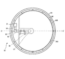
本発明の第1実施形態について図1及び図2を参照しつつ説明する。図1は、本実施形態の電子時計の外観を示す平面図である。図2は電子時計の概略を示す部分断面図である。
<A:電子時計の概要>
図1に示す電子時計100は、2.4GHz帯(ISM帯)を用いた近距離無線(Bluetooth(登録商標)など)による通信が可能な電子時計である。
図1及び図2に示すように、電子時計100は、外装ケース80を備えている。外装ケース80は、金属で形成された円筒状のケース胴81に、セラミックまたは金属で形成されたベゼル82が嵌合されて構成されている。なお、本実施形態では、外装ケースを2部品で構成したが、1部品で構成するようにしてもよい。
<First Embodiment>
A first embodiment of the present invention will be described with reference to FIGS. 1 and 2. FIG. 1 is a plan view showing the appearance of the electronic timepiece of the present embodiment. FIG. 2 is a partial sectional view showing an outline of the electronic timepiece.
<A: Outline of electronic watch>
An
As shown in FIGS. 1 and 2, the
ベゼル82の内周側に、リング状のダイヤルリング83を介して、円盤状の文字板11が配置され、この文字板11上には、時刻を表示する指針13やカレンダー等が配置されている。指針13は、時針13aと、分針13bと、秒針13cとから構成される。
外装ケース80の表面側の開口は、ベゼル82を介してカバーガラス84で塞がれており、カバーガラス84を通じて、内部の文字板11、指針13(時針13a、分針13b、秒針13c)が視認可能となっている。
A disc-shaped
The opening on the surface side of the
電子時計100は、リュウズ16を手動操作することにより、手動の時刻修正が可能であり、また、操作ボタン17を手動操作することにより、通常の時刻表示モードと通信モードとを切り替えることが可能に構成されている。
The
図2に示すように、電子時計100は、金属製の外装ケース80の2つの開口のうち、表面側の開口は、ベゼル82を介してカバーガラス84で塞がれており、裏面側の開口は金属で形成された裏蓋85で塞がれている。
As shown in FIG. 2, in the
ダイヤルリング83は、外周端が、ベゼル82の内周面に接触しているとともに、一面がカバーガラス84と平行な平板部分と、内周端が文字板11に接触するように、文字板11側へ傾斜した傾斜部分を備えている。ダイヤルリング83は、平面視においてはリング形状となっており、断面視においてはすり鉢形状となっている。
The
文字板11と、駆動機構140が取り付けられているムーブメント125との間には、第2基板135が備えられている。第2基板135には、アンテナエレメントとしてのチップアンテナ91、給電パターン94、及び接続点95が備えられている(図5C、図5D参照)。第2基板135はネジ(図示せず)等によりムーブメント125に取り付けられている。
A
ムーブメント125は、プラスチック部品で構成されており、内部には駆動機構140が設けられている。駆動機構140は、ステップモーターと歯車などの輪列とを有し、当該ステップモーターが当該輪列を介して指針軸14を回転させることにより、指針13が駆動する。
本実施形態においては、ムーブメント125の外周に固定リング状の中枠86を取り付け、中枠86とケース胴81により半径方向の位置決めを行い、中枠86とダイヤルリング83により上下方向の位置決めを行っている。
The
In the present embodiment, a fixed ring-shaped
ムーブメント125の裏面には、第1基板145がネジ(図示せず)等によりムーブメント125に取り付けられている。第1基板145は、通信部122、制御部150、及び電池130を備えている。また、第1基板145は、接続点95、給電パターン96、マッチング素子98、及び給電点97を備えている(図5D参照)。
A
上述した第2基板135と、ムーブメント125と、第1基板の一部には、貫通孔が形成されており、この貫通孔には、導通電極92が配置されている。導通電極92は、第2基板135上の接続点93及び給電パターン94を介してチップアンテナ91に接続されると共に、第1基板上の接続点95及び給電パターン96を介して給電点97に接続されている。詳しくは後述する。
A through hole is formed in a part of the
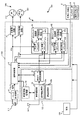
<B:電子時計の電気的構成>
本実施形態の電子時計100は、図2に示すように、Bluetooth(登録商標)の規格に従った無線通信を行う通信部122と、指針の駆動を制御する制御部150と、指針を駆動する駆動機構140と、電池130と、リュウズ16や操作ボタン17などの外部入力装置8とを備えて構成されている。
<B: Electrical configuration of electronic watch>
As shown in FIG. 2, the
通信部122は、アンテナ装置90と、時刻情報管理部22と、無線通信部23と、時刻データ記憶回路部24とを備えて構成されている。本実施形態では、通信部122は、Bluetooth(登録商標)の規格に従った無線通信を行うので、周波数としては2.4GHz帯を用いる。
アンテナ装置90は、アンテナエレメントとしてのチップアンテナ91、導通電極92、及び給電点97等により構成される。詳しくは後述する。
時刻情報管理部22は、CPU等により実現され、外部の電子機器との無線通信により取得した時刻情報に基づいて、現在の時刻を時刻情報に基づく時刻に修正する処理を行う。また、時刻情報管理部22は、電子機器との無線通信により電子時計100の現在の時刻を携帯機器に送信するための処理を行う。詳しくは後述する。
無線通信部23は、Bluetooth(登録商標)の規格に従った無線通信を行う専用のIC(集積回路装置)により実現される。無線通信部23は、コンデンサ等で構成された同調部及びパワーアンプ等で構成された送受信部を含む送受信回路部23aと、リンク層部及び制御処理部を含む通信処理部23bとを備える。送受信回路部23aは、電子機器との無線による情報の送受信を行う。通信処理部23bのリンク層部は、リンク層の処理、すなわち、機器同士の論理的な接続に関する処理を行う。通信処理部23bの制御処理部の機能は、CPU等の各種プロセッサやASIC等のハードウェア回路や、このハードウェア回路上で動作するプログラムなどにより実現できる。
時刻データ記憶回路部24は、メモリ等で構成され、無線通信部23で処理された時刻データを記憶する。
The
The
The time
The wireless communication unit 23 is realized by a dedicated IC (integrated circuit device) that performs wireless communication in accordance with the Bluetooth (registered trademark) standard. The wireless communication unit 23 includes a transmission / reception circuit unit 23a including a tuning unit configured by a capacitor and the like and a transmission / reception unit configured by a power amplifier and the like, and a
The time data
制御部150を構成する運針制御部3は、図3に示すように、パルス合成回路31からのパルス信号が入力される。パルス合成回路31は、水晶振動子などの基準振動子311からの基準パルスを分周してクロックパルスを生成し、また、基準パルスからパルス幅やタイミングの異なるパルス信号を発生させる。運針制御部3は、通常モード時においては、時刻情報管理部22から出力される時刻情報並びに前記クロックパルス及びパルス信号に基づいて、通常の時刻表示のために指針の駆動を制御する。
As shown in FIG. 3, the hand movement control unit 3 constituting the
運針制御部3は、通常モード時においては、一秒に一回出力され秒針を駆動させる秒駆動パルス信号と、一分間に一回出力され時分針を駆動させる時分駆動パルス信号とを、秒駆動回路41、時分駆動回路42に出力して、指針の駆動を制御する。すなわち、各駆動回路41,42は、各駆動回路41、42からのパルス信号によって駆動されるステッピングモータからなる秒モータ411,時分モータ421を駆動し、これにより各モータ411,421に接続された秒針13cと、分針13b及び時針13aとを駆動する。そして、各指針、モータ411,421、駆動回路41,42によって時刻を表示する時刻表示部が構成されている。なお、時刻表示部としては、1つのモータで、時針、分針、秒針を駆動するものでもよい。
In the normal mode, the hand movement control unit 3 outputs a second drive pulse signal that is output once per second to drive the second hand and an hour / minute drive pulse signal that is output once per minute to drive the hour / minute hand. Output to the
制御部150を構成するカウンタ部6は、秒をカウントする秒カウンタ回路部61と、時分をカウントする時分カウンタ回路部62とを備えて構成されている。
秒カウンタ回路部61は、秒位置カウンタ611と、秒時刻カウンタ612と、一致検出回路613とを備えて構成されている。秒位置カウンタ611及び秒時刻カウンタ612はともに60カウント、つまり1Hzの信号が入力された場合には60秒でループするカウンタである。秒位置カウンタ611は、運針制御部3から秒駆動回路41に供給される駆動パルス信号(秒駆動パルス信号PS1)をカウントしている。つまり、秒針を駆動させる駆動パルス信号をカウントすることによって、秒針が示している秒針の位置をカウントしている。
秒時刻カウンタ612は、通常は、運針制御部3から出力される1Hzの基準パルス信号(クロックパルス)をカウントする。また、時刻情報管理部22から時刻修正指示が出力された場合には、運針制御部3は、時刻データ記憶回路部24から時刻データを読み取り、この時刻データのうちの秒データに合わせてカウンタ値が修正される。
The
The second
The second time counter 612 normally counts a 1 Hz reference pulse signal (clock pulse) output from the hand movement control unit 3. When a time correction instruction is output from the time
同様に、時分カウンタ回路部62は、時分位置カウンタ621と、時分時刻カウンタ622と、一致検出回路623とを備えて構成されている。時分位置カウンタ621および時分時刻カウンタ622はともに24時間分の信号が入力されるとループするカウンタである。時分位置カウンタ621は、運針制御部3から時分駆動回路42に供給される駆動パルス信号(時分駆動パルス信号PS2)をカウントし、時針、分針が示している時分針の位置をカウントしている。
時分時刻カウンタ622は、通常は、運針制御部3から出力される1Hzのパルス(クロックパルス)をカウントする(正確には1Hzを60回計数したところで1カウントとする)。また、時刻情報管理部22から時刻修正指示が出力された場合には、運針制御部3は、時刻データ記憶回路部24から時刻データを読み取り、この時刻データのうちの時分データに合わせてカウンタ値が修正される。
Similarly, the hour / minute
The hour /
各一致検出回路613,623は、各位置カウンタ611,621と各時刻カウンタ612,622とのカウント値の一致を検出し、一致しているか否かを示す検出信号を運針制御部3に出力する。
運針制御部3は、各一致検出回路613,623から不一致信号が入力されると、一致信号が入力されるまで各駆動パルス信号を出力し続ける。このため、通常運針時は、運針制御部3から1Hzの基準信号によって各時刻カウンタ612,622のカウンタ値が変化して位置カウンタ611,621と不一致となると、各駆動パルス信号が出力されて各指針が動くとともに、各位置カウンタ611,621が時刻カウンタ612,622と一致することになり、この動作を繰り返すことで、通常の運針制御が行われる。
また、時刻データ記憶回路部24から読み取った時刻データで各時刻カウンタ612,622が修正されると、そのカウンタ値に各位置カウンタ611,621のカウンタ値が一致するまで、各駆動パルス信号が出力され続け、指針が早送りされて正しい時刻に修正される。
The
When a mismatch signal is input from each of the
When the time counters 612 and 622 are corrected with the time data read from the time data
電池130は、通信部122及び制御部150に電力を供給する。電池130は、銀電池等の一次電池を用いてもよいし、リチウムイオン電池のような二次電池を用いてもよい。
外部入力装置8は、リュウズ16、操作ボタン17を備え、受信動作や時刻合わせなどを行うために利用される。また、通常モードと通信モードの切り替えは、操作ボタン17を押下することにより行う。
The
The external input device 8 includes a
<C:電子時計におけるアンテナ装置の構成>
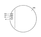
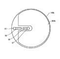
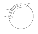
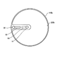
次に、電子時計100におけるアンテナ装置90の構成について図4Aないし図6を参照しつつ説明する。
図4Aは、カバーガラス84側からアンテナ装置90を見た場合の平面図であり、図4Bは、図4AのA―A’線断面図である。図5Aは第2基板135の表面側を示す平面図であり、図5Bは裏面側を示す平面図である。図5Cは第1基板145の表面側を示す平面図であり、図5Dは裏面側を示す平面図である。図6はアンテナ装置90の特性例を示す図である。なお、本実施形態においては、第2基板135、ムーブメント125、及び第1基板145を図4Bのようにケース胴81に収納した際に、第2基板135、ムーブメント125、及び第1基板145の面のうち、カバーガラス84側の面を表面、裏蓋85側の面を裏面とする。
<C: Configuration of antenna device in electronic timepiece>
Next, the configuration of the
4A is a plan view when the
本実施形態のアンテナ装置90は、金属製のケース胴81に取り付けられる金属製の裏蓋85側に設けられた第1基板145と、第1基板145に対してムーブメント125を挟んで配置された第2基板135とを備えている。
第1基板145は、図5以下の説明においては、アンテナ装置にかかわる部分のみ両面基板(2層基板)として説明してあり、ムーブメント125の裏面側に接する第1基板145の表面145aには、図5Cに示すように、グランドパターン200を構成する表面側グランドパターン200aと、導通電極92が取り付けられる接続点95が形成されている。接続点95は、導電性材料から形成されるパターンであり、導通電極92が貫通する貫通孔の内面側に導通パターンを形成してもよいし、導通電極92の端面が接触する平面の導通パターンとしてもよい。
The
In the description of FIG. 5 and the subsequent drawings, the
裏蓋85と対向する第1基板145の裏面145bには、図5Dに示すように、接続点95と、給電パターン96と、給電点97と、グランドパターン200を構成する裏面側グランドパターン200bとが形成されている。接続点95は、導電性の材料から形成されるパターンであり、第1基板145の表面145aの接続点95と電気的に導通している。第1基板145の裏面145bの接続点95についても、導通電極92が貫通する貫通孔の内面側に導通パターンを形成してもよいし、平面の導通パターンとしてもよい。給電パターン96は導電性材料から形成されるパターンであり、接続点95と給電点97にそれぞれ接続される。給電パターン96には、図4Aに示すように、π型3素子構成のマッチング素子98が接続される。給電点97は、アンテナに接続される回路の入出力点であり給電回路としての通電部122(図4A、図5Dにおいては図示を省略している)に接続される。また、裏面側グランドパターン200bと表面側グランドパターン200aは電気的に導通されている。
As shown in FIG. 5D, the
カバーガラス84と対向する第2基板135の表面135aには、図5Aに示すように、チップアンテナ取り付けパターン91a,91bと、給電パターン94と、接続点93とが形成されている。チップアンテナ取り付けパターン91a,91bは導電性材料から形成され、チップアンテナ取り付けパターン91a,91bには図4Aに示すように、チップアンテナ91が接続される。接続点93は、導電性材料から形成されるパターンであり、導通電極92が貫通する貫通孔の内面側に導通パターンを形成してもよいし、導通電極92の端面が接触する平面の導通パターンとしてもよい。給電パターン94は導電性材料から形成されるパターンであり、チップアンテナ取り付けパターン91bと接続点93にそれぞれ接続される。
As shown in FIG. 5A, chip
ムーブメント125の表面側に接する第2基板135の裏面135bには接続点93が形成されている。接続点93は、第2基板135の表面135aの接続点93と電気的に導通している。第2基板135の裏面135bの接続点93についても、導通電極92が貫通する貫通孔の内面側に導通パターンを形成してもよいし、平面の導通パターンとしてもよい。
A
上述した第1基板145及び第2基板135をムーブメント125にネジ(図示せず)等により取り付け、第1基板145及び第2基板135によりムーブメント125を挟むように構成する。そして、図4Bに示すように、第1基板145及び第2基板135並びにムーブメント125を貫通する導通電極92を配置し、導通電極92の一端部を第2基板135の接続点93に接続し、導通電極92の他端部を第1基板145の接続点95に接続する。
The
したがって、チップアンテナ91、給電パターン94、接続点93、導通電極92、接続点95、給電パターン96、マッチング素子98、及び給電点97は電気的に導通することになる。また、給電パターン96、マッチング素子98、及び給電点97の周囲は、グランドパターン200(表面側グランドパターン200a,裏面側グランドパターン200b)により囲まれており、これらにより、本発明のアンテナ装置90が構成される。
Therefore, the
つまり、本発明のアンテナ装置90は、電子時計100の金属製のケース胴81内に収納されるアンテナ装置であって、金属製のケース胴81の裏蓋85側に設けられ、グランドパターン200及び給電回路としての通電部122が形成された第1基板145と、電子時計100のムーブメント125を挟んで配置され、アンテナエレメントとしてのチップアンテナ91が形成された第2基板135と、ムーブメント125内に配置され、一端が給電点97を介して給電回路としての通電部122に接続されると共に、他端がアンテナエレメントとしてのチップアンテナ91に接続される導通電極92とを備え、グランドパターン200に対して、91〜96がモノポールを形成することを特徴とするアンテナ装置である。
In other words, the
以上のような構成により、本発明のアンテナ装置90は、グランドパターン200と給電回路としての通電部122を含む第1基板145を裏蓋85側に配置し、アンテナエレメントとしてのチップアンテナ91を第2基板135に配置し、両方の基板を貫通する導通電極92によって通電部122とチップアンテナ91を導通させるので、電子時計100のケース胴81という限られた空間内において、アンテナ装置を立体的に構成することができる。
With the configuration as described above, the
この立体構成は電子時計100に用いられている機械部品や、金属製のケース胴81に大きな構造上の変更を加えることなく実現することができ、本発明は、小型の金属製のケース胴81内に配置可能な新しいアンテナ装置90を提供する。まず、アンテナエレメントとしてのチップアンテナ91がカバーガラス84側に配置されることになり、面積の大きな金属製の裏蓋85から遠ざかることとなり、また、ムーブメント125内の機械部品の上面にアンテナエレメントとしてチップアンテナ91が配置されることになり、金属製の部材の影響を低減することができ、アンテナゲインの劣化が低減される。
This three-dimensional configuration can be realized without major structural changes to the mechanical parts used in the
また、導通電極92が、第1基板145、第2基板135、及びグランドパターン200に対して直立した立体構造となっているので、良好なアンテナ特性が得られ、ムーブメント125と金属製の裏蓋85が近接する構造においても、ゲインの劣化の少ない構造を提供することができる。さらに、給電回路としての通電部122を電池130側に設けることができるので、回路構成が容易となる。また、アンテナエレメントとしてのチップアンテナ91は第2基板135上に形成され、第2基板135はムーブメント125に固定されることにより、さらには、導通電極92についてもムーブメント125に内包されることにより、アンテナ位置のばらつきを低減できる。その結果、アンテナゲインのばらつきを低減することができる。
さらに、金属製のケース胴81内にアンテナ装置90を構成するにあたっては、アンテナエレメントとしてのチップアンテナ91またはプリントアンテナ99と金属製のケース胴81との位置関係によって、アンテナゲインが敏感に変化するため、両者間には一定のクリアランスを安定的に設けることが望ましい。本実施形態においては、ムーブメント125と金属製のケース胴81との間に固定リング状の中枠86を配置し、中枠86にムーブメントを125固定する。つまり、ムーブメント125は中枠86を介して金属製のケース胴81に取り付けられる。これにより、第2基板135に形成されたアンテナエレメントとしてのチップアンテナ91またはプリントアンテナ99はケース外周に対して、一定のクリアランスを設けて固定されることになる。したがって、アンテナゲインばらつきが抑制され、組み立て性を向上させることができる。
Further, since the
Furthermore, when the
図6に本発明のアンテナ装置90の特性例を示す。図6において、レーダーチャート軸の標記はアンテナゲインの相対値のデシベル表示であり、値が大きいほどアンテナゲインが大きいことを示す。
図6には。金属製の裏蓋85を装着した本発明のアンテナ装置90の特性例、金属製の裏蓋85を装着しない本発明のアンテナ装置90の特性例、及び、図11A、図11Bに示すプラスチックケースを用いた比較例の電子時計におけるアンテナ装置の特性例を示している。
FIG. 6 shows a characteristic example of the
In FIG. The characteristic example of the
図11A、図11Bに示す比較例は、ケースとしてプラスチック製のケース500を用いており、単一の回路基板501上に、チップアンテナ91、マッチング素子98、給電パターン96、給電点97が形成されている。
11A and 11B uses a
図6に示すように、本発明のアンテナ装置90は金属製の裏蓋85を装着しない場合には、比較例のプラスチック製のケース500内の回路基板501上のアンテナ装置に対して、特性を示すレーダーチャート図の面積が大きくなり、良好な特性を有していることがわかる。
また、金属製の裏蓋85を装着すると、裏蓋85を装着しない場合に比較して特性は劣化するものの、比較例のアンテナ装置の特性に対し、ほぼ同等の面積を有しているといえる。つまり、本発明のアンテナ装置90は、金属製の裏蓋85を用いているにも拘わらず、金属製の裏蓋85を用いない比較例のアンテナ装置と同等の特性が得られることがわかる。
As shown in FIG. 6, when the
Further, when the
また、本発明のアンテナ装置90には、次のような利点がある。つまり、本発明においては、グランドパターン200と、給電回路としての通電部122を第1基板145上に形成し、第2基板135にはアンテナエレメントとしてのチップアンテナ91を配置することにより、立体的なアンテナ装置が構成できるため、第2基板135に構成されるアンテナエレメントとして、チップアンテナ91という基本的なアンテナエレメントを用いることができる。
The
また、金属製のケース胴81内にアンテナ装置90を構成するにあたって、アンテナエレメントとしてのチップアンテナ91と金属製のケース胴81及び裏蓋85との位置関係によって、アンテナゲインが敏感に変化するが、両者間には一定のクリアランスを安定的に設けることが望ましい。本発明においては、ムーブメント125を挟むように第1基板145と第2基板135を取り付け、ムーブメント125をケース胴81に中枠86を介して位置決めするようにしたので、第2基板135に配置されたアンテナエレメントとしてのチップアンテナ91はケース胴81に対して、一定のクリアランスを設けて固定されることになる。これにより、アンテナゲインのばらつきが抑制され、組み立て性もまた向上する。
Further, when the
なお、本実施形態においては、第2基板135上にグランドパターンを設けていないため、第2基板135上のレイアウトの自由度を向上させることができる。すなわち第2基板135上にアンテナエレメントとしてチップアンテナ91、給電パターン94、及び接続点93のみを配置してもよいし、また、第2基板135のチップアンテナ91等以外の部分に他の回路パターンを形成してもよい。あるいは第2基板135のチップアンテナ91等以外の部分に金属板等の他の部品を配置しても、アンテナ特性に大きな劣化をもたらさず、良好なアンテナ装置を提供できる。
In this embodiment, since the ground pattern is not provided on the
<第2実施形態>
次に、本発明の第2実施形態について図7Aないし図7Dを参照しつつ説明する。本実施形態においては、図7A及び図7Bに示すように、第2基板135にグランドパターン201(表面側グランドパターン201a,裏面側グランドパターン201a)を形成している。
表面側グランドパターン201aは、アンテナエレメントとしてのチップアンテナ91と所定の距離を保って形成されている。
また、第1基板145においては、グランドパターン200(表面側グランドパターン200a,裏面側グランドパターン200a)の面積を第1実施形態よりも大きくしている。なお、第2基板135にグランドパターン201と第1基板145のグランドパターン200は電気的に導通している。
つまり、多層基板としての第1基板145において、グランドパターン200は第1基板145の各層に形成され、各層に形成されたグランドパターン200は、給電回路としての通電部122及び給電回路としての通電部122と導通電極92との接続箇所である給電点97を除く基板のほぼ全域にわたって形成されている。
Second Embodiment
Next, a second embodiment of the present invention will be described with reference to FIGS. 7A to 7D. In the present embodiment, as shown in FIGS. 7A and 7B, the ground pattern 201 (the front-
The front-
In the
That is, in the
本実施形態によれば、第2基板135のアンテナエレメントとしてチップアンテナ91及び導通電極92が、立体的に構成された第1基板145のグランドパターン200と第2基板135のグランドパターン201上に、立体的に構成される配置となり、立体的なモノポールアンテナとして動作することになる。したがって、金属製の裏蓋85の影響がより一層低減されることになる。
また、グランドパターンの面積が第1実施形態よりも大きくなるため、アンテナの指向性を理想的な指向性に近づけることができる。
According to the present embodiment, the
In addition, since the area of the ground pattern is larger than that of the first embodiment, the antenna directivity can be made closer to the ideal directivity.
<第3実施形態>
次に、本発明の第3実施形態について図8Aないし図10を参照しつつ説明する。本実施形態においては、図8Aないし図8D、及び図9Aないし図9Dに示すように、アンテナエレメントとして、4分の1波長のプリントアンテナ99を用いている。プリントアンテナ99は、導電性の材料により形成したパターンであり、容易に製造することができる。
プリントアンテナ99を用いる場合でも、図8A及び図8Bに示すように、第2基板135にグランドパターンを設けない構成としてもよいし、図9A及び図9Bに示すように、第2基板135にグランドパターン201を設ける構成としてもよい。
<Third Embodiment>
Next, a third embodiment of the present invention will be described with reference to FIGS. 8A to 10. In this embodiment, as shown in FIGS. 8A to 8D and FIGS. 9A to 9D, a quarter-wavelength printed
Even when the printed
図10に、図9A及び図9Bに示すように第2基板135にグランドパターン201を設けた場合のアンテナ装置90の特性例を示す。図10に示すように、プリントアンテナ99を用いた場合であっても、金属製の裏蓋85の有無に関して、第1実施形態と同様の変化があるものの、比較例におけるプラスチック製のケース500内のアンテナ装置に対し、ほぼ同等の特性を有していることがわかる。
FIG. 10 shows a characteristic example of the
つまり、本発明のアンテナ装置を用いることで、電子時計100において、金属製のケース胴81、金属製の裏蓋85、歯車などを構成する金属製の機械部品などが存在する場合においても、プラスチック製のケース500を有する比較例と同様に、アンテナゲインの劣化の少ない良好なアンテナ特性を得ることができる。
In other words, by using the antenna device of the present invention, the
<変形例>
本発明は、上述した実施形態に限定されるものではなく、例えば次に述べるような各種の変形が可能である。また、次に述べる変形の態様は、任意に選択された一または複数を、適宜に組み合わせることもできる。
<Modification>
The present invention is not limited to the above-described embodiments, and various modifications as described below are possible, for example. Moreover, the aspect of the deformation | transformation described below can also combine suitably arbitrarily selected 1 or several.
(変形例1)
上述した各実施形態におけるグランドパターン200,201は電子時計100の電池130のプラス電位またはマイナス電位と同電位とすればよい。このようにすれば、簡単な構成で、電子時計100の回路内のグランド電位を安定させることができる。
(Modification 1)
The
(変形例2)
上述した実施形態及び変形例においては、本発明をアナログ式の電子時計に適用したが、本発明は、置き時計型、もしくは、掛け時計型等の電子時計に適用可能である。
(Modification 2)
In the above-described embodiments and modifications, the present invention is applied to an analog electronic timepiece, but the present invention is applicable to an electronic timepiece such as a table clock type or a wall clock type.
上述した本発明の各機能は、例えば、CPU(中央処理装置)、メモリ(記憶装置)等を備えたコンピュータにプログラムを組み込んで実現させてもよい。なお、このプログラムは、インターネット等の通信手段や、CD−ROM、メモリカード等の記録媒体を介してインストールされてもよい。 Each function of the present invention described above may be realized by incorporating a program into a computer including a CPU (Central Processing Unit), a memory (storage device), and the like. This program may be installed via a communication means such as the Internet or a recording medium such as a CD-ROM or a memory card.
上述した実施形態及び各変形例においては、近距離無線通信の例として、Blooth(登録商標)の規格に従った無線通信を用いたが、本発明はこのような構成に限定されるものではなく、Wi―Fi(登録商標)他の近距離無線通信を用いた場合にも適用可能である。 In the embodiment and each modification described above, wireless communication in accordance with the Bluetooth (registered trademark) standard is used as an example of short-range wireless communication, but the present invention is not limited to such a configuration. Wi-Fi (registered trademark) and other short-range wireless communications are also applicable.
13…指針、13a…時針、13b…分針、13c…秒針、16…リュウズ、17…操作ボタン、80…外装ケース、81…ケース胴、82…ベゼル、83…ダイヤルリング、84…カバーガラス、85…裏蓋、86…中枠、90…アンテナ装置、91…チップアンテナ、92…導通電極、93…接続点、94…給電パターン、95…接続点、96…給電パターン、97…給電点、98…マッチング素子、100…電子時計、122…通信部、125…ムーブメント、200…グランドパターン、201…グランドパターン。
DESCRIPTION OF
Claims (9)
前記金属製ケース内に配置される前記電子時計のムーブメントと、前記金属製ケースの裏蓋との間に配置され、グランドパターン及び給電回路が設けられた第1基板と、
前記ムーブメントに取り付けられ、前記第1基板と前記電子時計のムーブメントを挟む位置に配置され、前記ムーブメントが向かい合う面と反対の面にアンテナエレメントが設けられた第2基板と、
前記第1基板と前記ムーブメントと前記第2基板とを貫通して配置され、一端が前記給電回路に接続され、他端が前記アンテナエレメントに接続される導通電極と、を備える、
ことを特徴とするアンテナ装置。 An antenna device housed in a metal case of an electronic watch,
A first substrate disposed between the movement of the electronic timepiece disposed in the metal case and the back cover of the metal case, and provided with a ground pattern and a power feeding circuit;
A second substrate attached to the movement, disposed at a position sandwiching the movement of the first substrate and the electronic timepiece, and having an antenna element on a surface opposite to a surface facing the movement ;
A conductive electrode disposed through the first substrate, the movement, and the second substrate, having one end connected to the feeder circuit and the other end connected to the antenna element;
An antenna device characterized by that.
Priority Applications (3)
| Application Number | Priority Date | Filing Date | Title |
|---|---|---|---|
| JP2015026181A JP6459593B2 (en) | 2015-02-13 | 2015-02-13 | Antenna device and electronic timepiece |
| CN201610080628.6A CN105892281A (en) | 2015-02-13 | 2016-02-04 | Antenna device and electronic timepiece |
| US15/040,261 US9979075B2 (en) | 2015-02-13 | 2016-02-10 | Antenna device and electronic timepiece |
Applications Claiming Priority (1)
| Application Number | Priority Date | Filing Date | Title |
|---|---|---|---|
| JP2015026181A JP6459593B2 (en) | 2015-02-13 | 2015-02-13 | Antenna device and electronic timepiece |
Publications (3)
| Publication Number | Publication Date |
|---|---|
| JP2016148611A JP2016148611A (en) | 2016-08-18 |
| JP2016148611A5 JP2016148611A5 (en) | 2017-11-30 |
| JP6459593B2 true JP6459593B2 (en) | 2019-01-30 |
Family
ID=56621405
Family Applications (1)
| Application Number | Title | Priority Date | Filing Date |
|---|---|---|---|
| JP2015026181A Active JP6459593B2 (en) | 2015-02-13 | 2015-02-13 | Antenna device and electronic timepiece |
Country Status (3)
| Country | Link |
|---|---|
| US (1) | US9979075B2 (en) |
| JP (1) | JP6459593B2 (en) |
| CN (1) | CN105892281A (en) |
Families Citing this family (4)
| Publication number | Priority date | Publication date | Assignee | Title |
|---|---|---|---|---|
| JP7283596B2 (en) * | 2017-02-27 | 2023-05-30 | カシオ計算機株式会社 | Electronic device manufacturing method and watch manufacturing method |
| JP6843663B2 (en) * | 2017-03-23 | 2021-03-17 | シチズン時計株式会社 | clock |
| JP7055038B2 (en) * | 2018-03-07 | 2022-04-15 | セイコーインスツル株式会社 | clock |
| JP7160066B2 (en) | 2020-05-28 | 2022-10-25 | カシオ計算機株式会社 | Antenna receiving device and electronic clock |
Family Cites Families (22)
| Publication number | Priority date | Publication date | Assignee | Title |
|---|---|---|---|---|
| JPS52150732U (en) * | 1976-05-11 | 1977-11-15 | ||
| JP3982918B2 (en) | 1998-08-07 | 2007-09-26 | 日本アンテナ株式会社 | Small receiver |
| US6531988B1 (en) * | 1999-09-28 | 2003-03-11 | Seiko Epson Corporation | Antenna device for high-frequency radio apparatus, high-frequency radio apparatus, and watch-shaped radio apparatus |
| US6762728B2 (en) * | 2000-03-29 | 2004-07-13 | Seiko Epson Corporation | Antenna device for high-frequency radio apparatus and wrist watch-type radio apparatus |
| JP2003152582A (en) | 2001-11-13 | 2003-05-23 | Seiko Epson Corp | Arm-worn electronic equipment with radio function |
| JP5082870B2 (en) | 2008-01-17 | 2012-11-28 | セイコーエプソン株式会社 | Wristwatch with wireless function |
| JP2010048605A (en) * | 2008-08-20 | 2010-03-04 | Seiko Epson Corp | Built-in antenna-type electronic timepiece |
| US8456949B2 (en) | 2008-12-03 | 2013-06-04 | Pgs Geophysical As | Method for determining signal quality in dual sensor seismic streamer signals |
| JP5251610B2 (en) * | 2009-03-03 | 2013-07-31 | Tdk株式会社 | ANTENNA DEVICE AND ANTENNA ELEMENT USED FOR THE SAME |
| JP5493527B2 (en) | 2009-07-14 | 2014-05-14 | セイコーエプソン株式会社 | Clock with wireless function |
| JP5610041B2 (en) | 2009-09-01 | 2014-10-22 | セイコーエプソン株式会社 | Antenna built-in clock |
| JP5609310B2 (en) | 2009-09-01 | 2014-10-22 | セイコーエプソン株式会社 | Antenna built-in clock |
| JP2011066648A (en) | 2009-09-17 | 2011-03-31 | Casio Computer Co Ltd | Antenna device and radio wave receiving device |
| JP2012093211A (en) | 2010-10-27 | 2012-05-17 | Seiko Epson Corp | Antenna built-in electronic timepiece |
| JP2012107955A (en) * | 2010-11-16 | 2012-06-07 | Seiko Epson Corp | Antenna built-in electronic timepiece |
| JP5866860B2 (en) * | 2011-01-05 | 2016-02-24 | セイコーエプソン株式会社 | Clock with wireless function |
| US9367043B2 (en) * | 2011-01-20 | 2016-06-14 | Seiko Epson Corporation | Satellite signal receiving device, method of controlling satellite signal receiving device, and electronic device |
| JP5715527B2 (en) | 2011-08-11 | 2015-05-07 | シチズンホールディングス株式会社 | Radio wave watch |
| JP5799703B2 (en) * | 2011-09-22 | 2015-10-28 | セイコーエプソン株式会社 | Electronic clock and secondary battery unit |
| JP5912763B2 (en) | 2012-03-29 | 2016-04-27 | シチズンホールディングス株式会社 | Clock with communication function |
| JP5344072B2 (en) * | 2012-09-05 | 2013-11-20 | セイコーエプソン株式会社 | Wristwatch with wireless function |
| JP6136380B2 (en) * | 2013-03-07 | 2017-05-31 | セイコーエプソン株式会社 | Electronic clock |
-
2015
- 2015-02-13 JP JP2015026181A patent/JP6459593B2/en active Active
-
2016
- 2016-02-04 CN CN201610080628.6A patent/CN105892281A/en active Pending
- 2016-02-10 US US15/040,261 patent/US9979075B2/en active Active
Also Published As
| Publication number | Publication date |
|---|---|
| US9979075B2 (en) | 2018-05-22 |
| CN105892281A (en) | 2016-08-24 |
| JP2016148611A (en) | 2016-08-18 |
| US20160240913A1 (en) | 2016-08-18 |
Similar Documents
| Publication | Publication Date | Title |
|---|---|---|
| JP5912763B2 (en) | Clock with communication function | |
| CN105676630B (en) | Electronic clock | |
| JP6459593B2 (en) | Antenna device and electronic timepiece | |
| JP6420794B2 (en) | Smart watch structure | |
| JP2017037057A (en) | Electronic watch | |
| JP2003152582A (en) | Arm-worn electronic equipment with radio function | |
| US11221591B2 (en) | Electronic timepiece having a conductive member spaced apart from a planar antenna | |
| JP6122261B2 (en) | Electronic device with communication function and electronic watch | |
| JP2019086415A (en) | Electronic timepiece | |
| JP5741734B2 (en) | Clock with wireless function | |
| WO2005119836A1 (en) | Portable electronic device | |
| JP2018169189A (en) | Radio-controlled timepiece | |
| JP5678972B2 (en) | Electronics | |
| JP2019056616A (en) | Portable radio-wave watch | |
| US20180299837A1 (en) | Antenna arrangement for an electronic device and an electronic device including same | |
| JP2020016563A (en) | Electronic watch | |
| US20190302703A1 (en) | Timepiece with Enhanced Antenna Arrangement | |
| US20230198566A1 (en) | Portable electronic object | |
| US20220269224A1 (en) | Electronic Timepiece | |
| JP7437287B2 (en) | Electronic clocks, electronic devices | |
| JP7414773B2 (en) | clock with solar panel | |
| JP2018109533A (en) | Radio-controlled clock | |
| US20210091471A1 (en) | Electronic watch with built-in antenna | |
| JP6821474B2 (en) | Radio clock | |
| JP2019039889A (en) | Portable atomic watch |
Legal Events
| Date | Code | Title | Description |
|---|---|---|---|
| A521 | Written amendment |
Free format text: JAPANESE INTERMEDIATE CODE: A523 Effective date: 20171017 |
|
| A621 | Written request for application examination |
Free format text: JAPANESE INTERMEDIATE CODE: A621 Effective date: 20171017 |
|
| A131 | Notification of reasons for refusal |
Free format text: JAPANESE INTERMEDIATE CODE: A131 Effective date: 20180904 |
|
| A977 | Report on retrieval |
Free format text: JAPANESE INTERMEDIATE CODE: A971007 Effective date: 20180831 |
|
| RD05 | Notification of revocation of power of attorney |
Free format text: JAPANESE INTERMEDIATE CODE: A7425 Effective date: 20180905 |
|
| A521 | Written amendment |
Free format text: JAPANESE INTERMEDIATE CODE: A523 Effective date: 20181012 |
|
| RD03 | Notification of appointment of power of attorney |
Free format text: JAPANESE INTERMEDIATE CODE: A7423 Effective date: 20181107 |
|
| TRDD | Decision of grant or rejection written | ||
| A01 | Written decision to grant a patent or to grant a registration (utility model) |
Free format text: JAPANESE INTERMEDIATE CODE: A01 Effective date: 20181204 |
|
| A61 | First payment of annual fees (during grant procedure) |
Free format text: JAPANESE INTERMEDIATE CODE: A61 Effective date: 20181217 |
|
| R150 | Certificate of patent or registration of utility model |
Ref document number: 6459593 Country of ref document: JP Free format text: JAPANESE INTERMEDIATE CODE: R150 |