JP6378515B2 - VLIW processor - Google Patents
VLIW processor Download PDFInfo
- Publication number
- JP6378515B2 JP6378515B2 JP2014063125A JP2014063125A JP6378515B2 JP 6378515 B2 JP6378515 B2 JP 6378515B2 JP 2014063125 A JP2014063125 A JP 2014063125A JP 2014063125 A JP2014063125 A JP 2014063125A JP 6378515 B2 JP6378515 B2 JP 6378515B2
- Authority
- JP
- Japan
- Prior art keywords
- data
- unit
- slot
- output
- bit data
- Prior art date
- Legal status (The legal status is an assumption and is not a legal conclusion. Google has not performed a legal analysis and makes no representation as to the accuracy of the status listed.)
- Active
Links
- 238000012545 processing Methods 0.000 claims description 169
- 238000000034 method Methods 0.000 claims description 87
- 101150099461 CTL2 gene Proteins 0.000 description 37
- 101150116431 Slc44a2 gene Proteins 0.000 description 37
- 238000010586 diagram Methods 0.000 description 31
- 230000001186 cumulative effect Effects 0.000 description 7
- 101100494773 Caenorhabditis elegans ctl-2 gene Proteins 0.000 description 4
- 238000012546 transfer Methods 0.000 description 4
- 101150050114 CTL1 gene Proteins 0.000 description 3
- 101100490488 Mus musculus Add3 gene Proteins 0.000 description 3
- 101150052401 slc44a1 gene Proteins 0.000 description 3
- 238000010977 unit operation Methods 0.000 description 3
- 230000005540 biological transmission Effects 0.000 description 2
- 238000005516 engineering process Methods 0.000 description 2
- 101100326920 Caenorhabditis elegans ctl-1 gene Proteins 0.000 description 1
- 238000007796 conventional method Methods 0.000 description 1
- 230000006870 function Effects 0.000 description 1
- 238000012986 modification Methods 0.000 description 1
- 230000004048 modification Effects 0.000 description 1
- 238000003672 processing method Methods 0.000 description 1
Images


Classifications
-
- G—PHYSICS
- G06—COMPUTING; CALCULATING OR COUNTING
- G06F—ELECTRIC DIGITAL DATA PROCESSING
- G06F9/00—Arrangements for program control, e.g. control units
- G06F9/06—Arrangements for program control, e.g. control units using stored programs, i.e. using an internal store of processing equipment to receive or retain programs
- G06F9/30—Arrangements for executing machine instructions, e.g. instruction decode
- G06F9/38—Concurrent instruction execution, e.g. pipeline or look ahead
- G06F9/3824—Operand accessing
- G06F9/3826—Bypassing or forwarding of data results, e.g. locally between pipeline stages or within a pipeline stage
-
- G—PHYSICS
- G06—COMPUTING; CALCULATING OR COUNTING
- G06F—ELECTRIC DIGITAL DATA PROCESSING
- G06F15/00—Digital computers in general; Data processing equipment in general
- G06F15/76—Architectures of general purpose stored program computers
-
- G—PHYSICS
- G06—COMPUTING; CALCULATING OR COUNTING
- G06F—ELECTRIC DIGITAL DATA PROCESSING
- G06F15/00—Digital computers in general; Data processing equipment in general
- G06F15/76—Architectures of general purpose stored program computers
- G06F15/82—Architectures of general purpose stored program computers data or demand driven
-
- G—PHYSICS
- G06—COMPUTING; CALCULATING OR COUNTING
- G06F—ELECTRIC DIGITAL DATA PROCESSING
- G06F9/00—Arrangements for program control, e.g. control units
- G06F9/06—Arrangements for program control, e.g. control units using stored programs, i.e. using an internal store of processing equipment to receive or retain programs
- G06F9/30—Arrangements for executing machine instructions, e.g. instruction decode
- G06F9/30003—Arrangements for executing specific machine instructions
- G06F9/30007—Arrangements for executing specific machine instructions to perform operations on data operands
- G06F9/3001—Arithmetic instructions
-
- G—PHYSICS
- G06—COMPUTING; CALCULATING OR COUNTING
- G06F—ELECTRIC DIGITAL DATA PROCESSING
- G06F9/00—Arrangements for program control, e.g. control units
- G06F9/06—Arrangements for program control, e.g. control units using stored programs, i.e. using an internal store of processing equipment to receive or retain programs
- G06F9/30—Arrangements for executing machine instructions, e.g. instruction decode
- G06F9/30098—Register arrangements
- G06F9/3012—Organisation of register space, e.g. banked or distributed register file
-
- G—PHYSICS
- G06—COMPUTING; CALCULATING OR COUNTING
- G06F—ELECTRIC DIGITAL DATA PROCESSING
- G06F9/00—Arrangements for program control, e.g. control units
- G06F9/06—Arrangements for program control, e.g. control units using stored programs, i.e. using an internal store of processing equipment to receive or retain programs
- G06F9/30—Arrangements for executing machine instructions, e.g. instruction decode
- G06F9/38—Concurrent instruction execution, e.g. pipeline or look ahead
- G06F9/3824—Operand accessing
-
- G—PHYSICS
- G06—COMPUTING; CALCULATING OR COUNTING
- G06F—ELECTRIC DIGITAL DATA PROCESSING
- G06F9/00—Arrangements for program control, e.g. control units
- G06F9/06—Arrangements for program control, e.g. control units using stored programs, i.e. using an internal store of processing equipment to receive or retain programs
- G06F9/30—Arrangements for executing machine instructions, e.g. instruction decode
- G06F9/38—Concurrent instruction execution, e.g. pipeline or look ahead
- G06F9/3836—Instruction issuing, e.g. dynamic instruction scheduling or out of order instruction execution
- G06F9/3853—Instruction issuing, e.g. dynamic instruction scheduling or out of order instruction execution of compound instructions
-
- G—PHYSICS
- G06—COMPUTING; CALCULATING OR COUNTING
- G06F—ELECTRIC DIGITAL DATA PROCESSING
- G06F9/00—Arrangements for program control, e.g. control units
- G06F9/06—Arrangements for program control, e.g. control units using stored programs, i.e. using an internal store of processing equipment to receive or retain programs
- G06F9/30—Arrangements for executing machine instructions, e.g. instruction decode
- G06F9/38—Concurrent instruction execution, e.g. pipeline or look ahead
- G06F9/3885—Concurrent instruction execution, e.g. pipeline or look ahead using a plurality of independent parallel functional units
- G06F9/3889—Concurrent instruction execution, e.g. pipeline or look ahead using a plurality of independent parallel functional units controlled by multiple instructions, e.g. MIMD, decoupled access or execute
Landscapes
- Engineering & Computer Science (AREA)
- Theoretical Computer Science (AREA)
- Software Systems (AREA)
- Physics & Mathematics (AREA)
- General Physics & Mathematics (AREA)
- General Engineering & Computer Science (AREA)
- Computer Hardware Design (AREA)
- Computational Mathematics (AREA)
- Mathematical Analysis (AREA)
- Mathematical Optimization (AREA)
- Pure & Applied Mathematics (AREA)
- Executing Machine-Instructions (AREA)
- Advance Control (AREA)
Description
本発明は、VLIW(Very long instruction word)アーキテクチャを採用するプロセッサ(VLIWプロセッサ)に関する。 The present invention relates to a processor (VLIW processor) that adopts a VLIW (Very Long Instruction Word) architecture.
画像データのような大容量データに対して効率良く演算処理を行うために、多様なプロセッサ技術が開発されている。 Various processor technologies have been developed in order to efficiently perform arithmetic processing on large-capacity data such as image data.
例えば、特許文献1には、グラフィックス処理用の画像処理プロセッサであって、ロード/ストアユニットと、複数の演算ユニットと、複数の演算ユニットの間において、ある演算ユニットの演算結果を、他の演算ユニットに入力させるための切り替えチャネルとを備える画像処理プロセッサの開示がある。 For example, Patent Document 1 discloses an image processing processor for graphics processing, in which a calculation result of a certain calculation unit is transferred to another load / store unit, a plurality of calculation units, and a plurality of calculation units. There is a disclosure of an image processor that includes a switching channel for input to an arithmetic unit.
ところで、従来のプロセッサにおいて、画像処理や画像認識処理を実行する場合、主として、8ビットあるいは16ビット単位での演算が実行されていた。近年、画像処理や画像認識処理の高度化・複雑化に伴い、画像処理や画像認識処理を実行するためのプロセッサでは、32ビット単位の演算を実行する割合が大幅に増えてきている。 By the way, in the conventional processor, when image processing or image recognition processing is executed, operations in units of 8 bits or 16 bits are mainly executed. In recent years, with the sophistication and complexity of image processing and image recognition processing, the ratio of executing arithmetic operations in units of 32 bits has greatly increased in processors for executing image processing and image recognition processing.
これに伴い、8ビットあるいは16ビット単位での演算だけでなく、32ビット単位の演算にも対応可能なプロセッサ(VLIWプロセッサ)が求められている。 Accordingly, there is a demand for a processor (VLIW processor) that can handle not only operations in units of 8 bits or 16 bits but also operations in units of 32 bits.
例えば、特許文献1の技術を用いて、16ビット単位での演算だけでなく、32ビット単位の演算にも対応可能なプロセッサを構成する場合、図13に示すような構成が考えられる。 For example, in the case of configuring a processor that can handle not only operations in 16-bit units but also operations in 32-bit units using the technique of Patent Document 1, a configuration as shown in FIG. 13 can be considered.
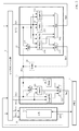
図13は、従来技術を用いて構成した32ビット単位の演算にも対応可能なプロセッサ900の概略構成図である。
FIG. 13 is a schematic configuration diagram of a
図13に示すように、プロセッサ900は、命令制御部91と、切替チャネル92と、命令実行部93と、命令メモリM91と、データメモリM92とを備える。
As illustrated in FIG. 13, the
命令制御部91は、命令メモリM91から命令を読み出し(命令フェッチ処理を行い)、読み出した命令をデコードする(命令デコード処理を行う)。そして、命令制御部91は、命令デコード処理の結果に基づいて、切替チャネル92および命令実行部93に対する制御を行う。
The
命令実行部93は、1サイクル(1クロックサイクル)で複数の命令を同時実行するために、1サイクルで同時に演算可能な複数の命令スロットを備える。命令実行部93は、図13に示すように、3つのスロット、すなわち、第1スロット931、第2スロット932、および、第3スロット933を有している。
The
第1スロット931は、データメモリM92に対してデータのロード/ストアを行うロード/ストアユニットを有している。
The
第2スロット932は、32ビット演算を行う加算ユニット(図13に「Add32」で示したユニット)と、16ビット演算を行う論理演算ユニット(図13に「Logic16」で示したユニット)と、32ビット演算を行うシフト演算ユニット(図13に「Shift32」で示したユニット)とを有している。
The
第3スロット933は、16ビット演算を行う加算ユニット(図13に「Add16」で示したユニット)と、16ビット演算を行う論理演算ユニット(図13に「Logic16」で示したユニット)と、16ビット演算を行う乗算ユニット(図13に「Mul16」で示したユニット)とを有している。
The
命令メモリM91は、プロセッサ900で、演算を実行するための命令等を記憶する記憶装置である。
The instruction memory M91 is a storage device that stores instructions and the like for executing operations in the
データメモリM92は、プロセッサ900で、演算を実行するためのデータ等を記憶することができる記憶装置である。
The data memory M92 is a storage device that can store data or the like for executing calculations in the
図13から分かるように、プロセッサ900では、第2スロット932に、32ビット演算を行うユニットを設けたので、切替チャネル92から、第2スロット932に、32ビットのデータを2つ分送信する必要がある。例えば、加算ユニットAdd16にて、32ビットデータの加算演算を行う場合、2つの32ビットデータが必要となる。このため、プロセッサ900では、図13に示すように、切替チャネル92と第2スロット932との間に16ビットデータの転送用パスが4つ(データパスDi92〜Di95)必要となる。つまり、プロセッサ900において、切替チャネル92と第2スロット932との間に、64ビット分のデータパスが必要となる。
As can be seen from FIG. 13, the
また、第2スロット932で32ビット演算が実行された場合、その出力結果は、32ビットデータとなるため、当該出力結果を、第2スロット932から切替チャネル92に送信するために、32ビット分のデータパスが必要となる。図13では、16ビットのデータ転送用のデータパスDo92、Do93により、第2スロット932から切替チャネル92に送信するために、32ビット分のデータパスを確保している。
Further, when a 32-bit operation is executed in the
また、プロセッサ900では、第3スロット933に、出力結果が32ビットとなる16ビットデータの乗算を行う乗算ユニットMul16を設けたので、当該出力結果を、第3スロット933から切替チャネル92に送信するために、32ビット分のデータパスが必要となる。図13では、16ビットのデータ転送用のデータパスDo94、Do95により、第3スロット933から切替チャネル92に送信するために、32ビット分のデータパスを確保している。
In the
このように、従来技術を用いて、32ビット単位の演算にも対応可能なプロセッサ900を構成した場合、切替チャネル92と命令実行部93との間に設置しなければならない入出力ポート数が多くなり、回路規模の増大を招く。また、切替チャネル92を、例えば、汎用レジスタファイルに置換する構成も考えられるが、この場合であっても、汎用レジスタファイルと命令実行部93との間に設置しなければならない入出力ポート数が多くなり、回路規模の増大を招く。
As described above, when the
そこで、本発明は、上記問題点に鑑み、回路規模の増大を抑えつつ、画像処理、画像認識処理等で多用される命令フローのようにビット拡張された演算を含む場合であっても、効率良く処理を実行することができるVLIWプロセッサを実現することを目的とする。 Therefore, in view of the above problems, the present invention is efficient even if it includes a bit-extended operation such as an instruction flow frequently used in image processing, image recognition processing, etc. while suppressing an increase in circuit scale. It is an object to realize a VLIW processor that can execute processing well.
上記課題を解決するために、第1の発明は、レジスタファイル部と、命令実行部と、を備えるVLIWプロセッサである。 In order to solve the above problems, a first invention is a VLIW processor including a register file unit and an instruction execution unit.
命令実行部は、第1スロットと、Nビット分(N:自然数)のデータを格納することができるステートレジスタと、を含む。 The instruction execution unit includes a first slot and a state register that can store data of N bits (N: natural number).
第1スロットは、レジスタファイル部からの出力データを入力するためのN×2ビット(N:自然数)の入力ポートと、レジスタファイル部にデータを出力するためのNビットの第1出力ポートと、ステートレジスタにデータを出力するためのNビットの第2出力ポートと、を含む。また、第1スロットは、Nビットデータに対して演算処理を行うことで、2×Nビットデータの出力データを取得する第1スロット用第1拡張演算ユニットを含む。 The first slot has an N × 2 bit (N: natural number) input port for inputting output data from the register file unit, an N-bit first output port for outputting data to the register file unit, And an N-bit second output port for outputting data to the state register. The first slot includes a first extended arithmetic unit for the first slot that obtains output data of 2 × N-bit data by performing arithmetic processing on the N-bit data.
そして、第1スロットは、第1スロット用第1拡張演算ユニットにより取得された2×Nビットデータの出力データのうちのNビット分のデータを、第1データとして、第1出力ポートからレジスタファイル部に出力し、第1スロット用第1拡張演算ユニットにより取得された2×Nビットデータの出力データのうちの第1データを除くNビット分のデータを、第2データとして、前記ステートレジスタに出力する。 The first slot uses the register file from the first output port as N-bit data out of the output data of 2 × N-bit data acquired by the first extended arithmetic unit for the first slot as the first data. N-bit data excluding the first data out of the output data of 2 × N-bit data obtained by the first extended arithmetic unit for the first slot is output to the state register as second data. Output.
このVLIWプロセッサでは、第1スロットが、第1スロット用第1拡張演算ユニットにより取得された2×Nビットデータを、Nビットずつに分けた2つのデータとして、レジスタファイル部およびステートレジスタに出力する。つまり、このVLIWプロセッサでは、処理対象が2×Nビットデータとなる2×Nビット演算を実行する場合であっても、当該2×NビットデータのうちのNビットデータが、ステートレジスタにより、保持され、例えば、次のサイクル(クロックサイクル)において、所定の演算ユニットにより利用することができる。 In this VLIW processor, the first slot outputs the 2 × N-bit data acquired by the first extended arithmetic unit for the first slot to the register file unit and the state register as two data divided into N bits. . In other words, in this VLIW processor, even when a 2 × N-bit operation in which the processing target is 2 × N-bit data is executed, the N-bit data of the 2 × N-bit data is held by the state register. For example, in the next cycle (clock cycle), it can be used by a predetermined arithmetic unit.
また、このVLIWプロセッサでは、第1スロットにおいて、レジスタファイル部からの入力ポートは、N×2ビット(N×2ビット分の入力ポート)であり、レジスタファイル部への出力ポートは、Nビット(Nビット分の出力ポート)であるため、VLIWプロセッサが、Nビット演算のみを実行する場合に比べて、入出力ポート数を増やす必要がない。 In the VLIW processor, in the first slot, the input port from the register file unit is N × 2 bits (input port for N × 2 bits), and the output port to the register file unit is N bits ( Therefore, it is not necessary for the VLIW processor to increase the number of input / output ports as compared with the case where the VLIW processor executes only N-bit operations.
このように、VLIWプロセッサでは、上記の通り、レジスタファイル部の入出力ポート数を増加させることなく、2×Nビットの演算をサポートすることが可能となる。 As described above, the VLIW processor can support a 2 × N-bit operation without increasing the number of input / output ports of the register file unit.
したがって、VLIWプロセッサでは、回路規模の増大を抑えつつ、画像処理、画像認識処理等で多用される命令フローのようにビット拡張された演算(N×2ビット演算)を含む場合であっても、効率良く処理を実行することができる。 Therefore, even if the VLIW processor includes an operation (N × 2 bit operation) that is bit-extended like an instruction flow frequently used in image processing, image recognition processing, etc. while suppressing an increase in circuit scale, Processing can be executed efficiently.
第2の発明は、第1の発明であって、第1スロットは、第1スロットからステートレジスタに出力され、ステートレジスタにより保持されている第2データを入力する。 2nd invention is 1st invention, Comprising: The 1st slot outputs the 2nd data currently output to the state register from the 1st slot, and is hold | maintained by the state register.
これにより、このVLIWプロセッサでは、例えば、1つ前のサイクルにおいて、第1スロットから出力されたNビットデータを、現在のサイクルにおいて、ステートレジスタから第1スロットに入力させ、第1スロットでの演算に用いることができる。 Thereby, in this VLIW processor, for example, the N-bit data output from the first slot in the previous cycle is input from the state register to the first slot in the current cycle, and the operation in the first slot is performed. Can be used.
第3の発明は、第1の発明であって、命令実行部は、第2スロットをさらに備える。 The third invention is the first invention, wherein the instruction execution unit further comprises a second slot.
第2スロットは、レジスタファイル部からの出力データを入力するためのN×2ビット(N:自然数)の入力ポートと、レジスタファイル部にデータを出力するためのNビットの出力ポートと、Nビットデータに対して処理の演算を行う第2スロット用第1演算ユニットと、
を含む。
The second slot has an N × 2 bit (N: natural number) input port for inputting output data from the register file unit, an N bit output port for outputting data to the register file unit, and N bits A first arithmetic unit for a second slot that performs processing operations on data;
including.
そして、第1スロットは、第1スロットから前記レジスタファイル部に出力され、レジスタファイル部により保持されている前記第1データを入力する。 The first slot receives the first data output from the first slot to the register file unit and held by the register file unit.
ステートレジスタは、第1スロットから出力された第2データを、第2スロットに出力する。 The state register outputs the second data output from the first slot to the second slot.
これにより、このVLIWプロセッサでは、例えば、1つ前のサイクルにおいて、第1スロットから出力されたNビットデータを、現在のサイクルにおいて、ステートレジスタから第2スロットに入力させ、第2スロットでの演算に用いることができる。 As a result, in this VLIW processor, for example, the N-bit data output from the first slot in the previous cycle is input from the state register to the second slot in the current cycle, and the operation in the second slot is performed. Can be used.
第4の発明は、第3の発明であって、第2スロットは、Nビットデータを読み出す読み出し部をさらに含む。 4th invention is 3rd invention, Comprising: The 2nd slot further contains the read-out part which reads N bit data.
第2スロットの読み出し部は、ステートレジスタから出力されるデータを読み出し、読み出したデータを、レジスタファイル部に出力する。 The reading unit of the second slot reads the data output from the state register, and outputs the read data to the register file unit.
このVLIWプロセッサでは、第2スロットの読み出し部により、ステートレジスタに保持されているNビットデータを読み出し、所定のタイミングで、レジスタファイル部に出力することができるため、2×Nビットデータを扱う演算が存在していても効率良くレジスタファイル部に所定のデータを出力し、レジスタファイル部において、必要なデータを保持させることができる。 In this VLIW processor, N-bit data held in the state register can be read out by the reading unit in the second slot and output to the register file unit at a predetermined timing. Even if the data exists, predetermined data can be efficiently output to the register file unit, and necessary data can be held in the register file unit.
第5の発明は、第3または第4の発明であって、第2スロットは、レジスタファイル部から出力されるデータ、および、ステートレジスタから出力されるデータのいずれか一方のデータを選択し、選択したデータを第2スロット用第1演算ユニットに入力させる第2スロット用選択部をさらに含む。 5th invention is 3rd or 4th invention, 2nd slot selects either one of the data output from a register file part, and the data output from a state register, It further includes a second slot selector for inputting the selected data to the second slot first arithmetic unit.
これにより、このVLIWプロセッサでは、第2スロット用第1演算ユニットに、レジスタファイル部から出力されるデータ、および、ステートレジスタから出力されるデータのいずれか一方を選択して入力させることができるので、必要なデータを、第2スロット用第1演算ユニットに、入力することができる。例えば、第2スロット用第1演算ユニットが加減算処理を行う演算ユニットである場合、当該演算ユニットをNビットデータの加減算処理に用いる場合、第1選択部により、レジスタファイル部から出力される2つのNビットデータが入力されるようにすることができる。一方、上記演算ユニットを2×Nビットデータの加減算処理の上位Nビット分の加減算処理に用いる場合、ステートレジスタに2×Nビットデータのうちの上位Nビット分のデータ(例えば、第1スロットの加算演算ユニットで取得されたNビット分のデータ)を保持し、第2スロット用選択部により、ステートレジスタの出力が上記演算ユニットに入力されるようにし、さらに、当該上位Nビット分のデータと加算する2×Nビットデータの上位Nビットデータをレジスタファイル部から入力されるようにすればよい。これにより、当該演算ユニットにおいて、2×Nビットデータの加減算処理の上位Nビットデータの加減算処理を実行することができる。 As a result, in this VLIW processor, the first arithmetic unit for the second slot can select and input either the data output from the register file unit or the data output from the state register. Necessary data can be input to the first arithmetic unit for the second slot. For example, when the first arithmetic unit for the second slot is an arithmetic unit that performs addition / subtraction processing, when the arithmetic unit is used for addition / subtraction processing of N-bit data, the first selection unit outputs two data output from the register file unit. N-bit data can be input. On the other hand, when the above arithmetic unit is used for addition / subtraction processing of upper N bits of addition / subtraction processing of 2 × N-bit data, data of upper N bits of 2 × N-bit data (for example, in the first slot) N-bit data acquired by the addition arithmetic unit) is held, and the output of the state register is input to the arithmetic unit by the second slot selection unit. The upper N bit data of the 2 × N bit data to be added may be input from the register file unit. Thereby, in the said arithmetic unit, the addition / subtraction process of the high-order N bit data of the addition / subtraction process of 2xN bit data can be performed.
第6の発明は、第5の発明であって、第1スロットは、Nビットデータに対して処理の演算を行う第1スロット用第1演算ユニットをさらに含む。 6th invention is 5th invention, Comprising: The 1st slot further contains the 1st operation unit for 1st slots which performs the calculation of a process with respect to N bit data.
第1スロット用第1拡張演算ユニットは、2つのNビットデータに対して、乗算処理を行う第1スロット用乗算ユニットである。 The first extended arithmetic unit for the first slot is a first slot multiplication unit that performs multiplication processing on two N-bit data.
第1データは、第1スロット用乗算ユニットが乗算処理により取得した2×Nビットデータのうちの下位Nビットのデータである。 The first data is lower N bits of the 2 × N bit data obtained by the multiplication process by the first slot multiplication unit.
第2データは、第1スロット用乗算ユニットが乗算処理により取得した2×Nビットデータのうちの上位Nビットのデータである。 The second data is the upper N bits of the 2 × N bit data obtained by the multiplication processing by the first slot multiplication unit.
第1スロット用第1演算ユニットは、2つのNビットデータに対して、加減算処理を行う第1スロット用加減算ユニットである。 First arithmetic unit for the first slot, for the two N-bit data, a first slot for pressurized decrease calculation unit that performs addition and subtraction processing.
第2スロット用第1演算ユニットは、2つのNビットデータに対して、加減算処理を行う第2スロット用加減算ユニットである。 First arithmetic unit for the second slot, for the two N-bit data, a second slot for pressurized decrease calculation unit that performs addition and subtraction processing.
これにより、第1スロットに、Nビットの乗算を行うユニット(乗算ユニット)と、Nビットの加減算処理を行うユニット(下位Nビットデータの加算ユニット)を割り当て、第2スロットに、Nビットの加減算処理を行うユニット(上位Nビットデータの加算ユニット)を割り当てることができる。 As a result, a unit that performs N-bit multiplication (multiplication unit) and a unit that performs N-bit addition / subtraction processing (lower N-bit data addition unit) are assigned to the first slot, and N-bit addition / subtraction is assigned to the second slot. A unit for processing (upper N-bit data addition unit) can be assigned.
第7の発明は、第3から第6のいずれかの発明であって、ステートレジスタは、保持しているNビットデータを、第1スロットに出力する。 The seventh invention is any one of the third to sixth inventions, wherein the state register outputs the N-bit data held therein to the first slot.
第1スロットは、第1スロット用第2拡張演算ユニットと、第1スロット用第1演算ユニットと、第1スロット用選択部と、をさらに含む。 The first slot further includes a second extended arithmetic unit for the first slot, a first arithmetic unit for the first slot, and a selection unit for the first slot.
第1スロット用第2拡張演算ユニットは、Nビットデータに対して演算処理を行うことで、2×Nビットデータの出力データを取得する。 The second extended arithmetic unit for the first slot obtains output data of 2 × N bit data by performing arithmetic processing on the N bit data.
第1スロット用第1演算ユニットは、Nビットデータに対して処理の演算を行う。 The first arithmetic unit for the first slot performs processing arithmetic on N-bit data.
第1スロット用選択部は、レジスタファイル部から出力されるデータ、および、ステートレジスタから出力されるデータのいずれか一方のデータを選択し、選択したデータを第1スロット用第2拡張演算ユニットに入力させる。 The selection unit for the first slot selects one of the data output from the register file unit and the data output from the state register, and the selected data is used as the second extended arithmetic unit for the first slot. Let them enter.
これにより、このVLIWプロセッサでは、例えば、1つ前のサイクルにおいて、第1スロットから出力されたNビットデータを、現在のサイクルにおいて、ステートレジスタから第1スロットの第1スロット用第2拡張演算ユニットに入力させ、当該演算ユニットでの演算に用いることができる。 Thereby, in this VLIW processor, for example, the N-bit data output from the first slot in the previous cycle is changed from the state register to the second extended arithmetic unit for the first slot in the first slot in the current cycle. And can be used for computation in the computation unit.
第8の発明は、第7の発明であって、第1スロット用第2拡張演算ユニットは、2つのNビットデータに対して、シフト演算を行い、2×Nビットデータの出力データを取得する第1スロット用シフト演算ユニットである。 The eighth invention is the seventh invention, wherein the second extended arithmetic unit for the first slot performs a shift operation on two N-bit data and obtains output data of 2 × N-bit data This is a shift operation unit for the first slot.
これにより、このVLIWプロセッサでは、第1スロット用シフト演算ユニットにより、例えば、ステートレジスタから出力されたNビットデータと、レジスタファイル部から出力されたNビットデータとを用いて、シフト演算処理を実行することができる。 As a result, in this VLIW processor, the shift operation unit for the first slot executes, for example, shift operation processing using N-bit data output from the state register and N-bit data output from the register file unit. can do.
第9の発明は、第8の発明であって、第1スロット用シフト演算ユニットは、シフト演算の処理対象のデータの上位Nビットデータを、第1スロット用選択部から出力されるデータとして、シフト演算を行う。 A ninth invention is the eighth invention, wherein the shift operation unit for the first slot uses the upper N bit data of the data to be processed for the shift operation as data output from the selection unit for the first slot, Perform a shift operation.
これにより、このVLIWプロセッサでは、第1スロット用シフト演算ユニットにより、例えば、ステートレジスタから出力されたNビットデータを上位Nビットデータとし、レジスタファイル部から出力されたNビットデータを下位Nビットデータとして、シフト演算処理を実行することができる。 Thus, in this VLIW processor, for example, the N-bit data output from the state register is converted into the upper N-bit data and the N-bit data output from the register file unit is converted into the lower N-bit data by the first slot shift operation unit. As a result, a shift calculation process can be executed.
第10の発明は、第6の発明であって、レジスタファイル部は、第1スロット用加減算ユニットの加減算処理により取得されるキャリーフラグを格納する領域を有している。 A tenth invention is the invention of the sixth register file unit has an area for storing a carry flag which is obtained by addition and subtraction of the pressure decrease calculation unit for the first slot.
第2スロット用加減算ユニットは、レジスタファイル部に格納されているキャリーフラグを用いて、2つのNビットデータに対して、加減算処理を行う。 Second slot for pressurized decrease calculation unit, by using the carry flag stored in the register file unit, for two N-bit data, performs addition and subtraction processing.
これにより、このVLIWプロセッサでは、例えば、第1スロットの演算ユニットでの加減算処理により生成されたキャリーフラグであって、レジスタファイル部に格納されたキャリーフラグを用いて、第2スロット用加減算ユニットが、2つのNビットデータに対する加減算処理を実行することができる。 Thus, in this VLIW processor, for example, a carry flag generated by the subtraction processing in the arithmetic units of the first slot, with the carry flag stored in the register file unit, down pressure for the second slot calculation The unit can perform addition / subtraction processing on two N-bit data.
第11の発明は、第6の発明であって、第2スロット用加減算ユニットは、加減算処理の処理対象の一方のNビットデータを、第2スロット用選択部から出力されるデータとして、加減算処理を行う。 An eleventh invention is the invention of the sixth, the second slot for pressurized decrease calculation unit, the one of the N-bit data to be processed in the subtraction process, as data that is output from the second slot selection unit, Addition / subtraction processing is performed.
これにより、第2スロットにおいても、ステートレジスタに保持されているデータを利用することが可能となり、Nビットデータの演算処理(例えば、Nビットデータの加減算処理)および2×Nビットの演算処理(拡張演算処理(例えば、2×Nビットデータの加減算処理))を効率良く実行することが可能となる。 As a result, even in the second slot, the data held in the state register can be used, and N-bit data arithmetic processing (for example, N-bit data addition / subtraction processing) and 2 × N-bit arithmetic processing ( It is possible to efficiently execute the extended arithmetic processing (for example, 2 × N-bit data addition / subtraction processing).
第12の発明は、第1から第11のいずれかの発明であって、命令実行部は、第3スロットをさらに備える。 The twelfth invention is any one of the first to eleventh inventions, wherein the instruction execution unit further includes a third slot.
第3スロットは、レジスタファイル部からの出力データを入力するためのN×2ビット(N:自然数)の入力ポートと、レジスタファイル部にデータを出力するためのNビットの出力ポートと、所定のメモリからデータを取得するロード処理、および、前記所定のメモリにデータを格納するストア処理の少なくとも一方の処理を行うロード/ストアユニットと、を含む。 The third slot has an N × 2 bit (N: natural number) input port for inputting output data from the register file part, an N bit output port for outputting data to the register file part, A load / store unit that performs at least one of a load process for acquiring data from the memory and a store process for storing data in the predetermined memory.
これにより、ロード/ストアユニットを含む第3スロットを備えるVLIWプロセッサを実現することができる。 As a result, a VLIW processor including the third slot including the load / store unit can be realized.
第13の発明は、第1から第12のいずれかの発明であって、第1データは、第1スロット用第1拡張演算ユニットにより取得された2×Nビットデータの出力データのうちの下位Nビット分のデータである。 A thirteenth aspect of the invention is any one of the first to twelfth aspects of the invention, wherein the first data is a lower order of the output data of 2 × N-bit data obtained by the first extended arithmetic unit for the first slot. N bits of data.
第2データは、第1スロット用第1拡張演算ユニットにより取得された2×Nビットデータの出力データのうちの上位Nビット分のデータである。 The second data is data for the upper N bits of the output data of 2 × N bit data acquired by the first extended arithmetic unit for the first slot .
これにより、このVLIWプロセッサでは、第1データ(レジスタファイル部に出力するデータ)を下位Nビットデータとし、第2データ(ステートレジスタに出力するデータ)を上位Nビットデータとして、効率良く演算処理を実行することができる。 As a result, in this VLIW processor, the first data (data to be output to the register file unit) is the lower N-bit data, and the second data (data to be output to the state register) is the upper N-bit data for efficient arithmetic processing. Can be executed.
本発明によれば、回路規模の増大を抑えつつ、画像処理、画像認識処理等で多用される命令フローのようにビット拡張された演算を含む場合であっても、効率良く処理を実行することができるVLIWプロセッサを実現することができる。 According to the present invention, while suppressing an increase in circuit scale, even when a bit-extended operation such as an instruction flow frequently used in image processing, image recognition processing, or the like is included, processing can be executed efficiently. It is possible to realize a VLIW processor capable of
[第1実施形態]
第1実施形態について、図面を参照しながら、以下、説明する。
[First Embodiment]
The first embodiment will be described below with reference to the drawings.
<1.1:VLIWプロセッサの構成>
図1は、第1実施形態に係るVLIWプロセッサ1000の概略構成図である。
<1.1: Configuration of VLIW processor>
FIG. 1 is a schematic configuration diagram of a
VLIWプロセッサ1000は、Nビット(N:自然数)単位の演算、および、2×Nビット単位の演算を行うVLIWプロセッサである。
The
なお、以下では、説明便宜のため、N=16、つまり、VLIWプロセッサ1000が、16ビット単位の演算および32ビット単位の演算を行うVLIWプロセッサである場合について、説明する。
In the following, for convenience of explanation, a case will be described in which N = 16, that is, the
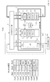
VLIWプロセッサ1000は、図1に示すように、命令制御部1と、レジスタファイル部2と、命令実行部3と、命令メモリM1と、データメモリM2とを備える。
As shown in FIG. 1, the
命令制御部1は、命令メモリM1から命令を読み出し(命令フェッチ処理を行い)、読み出した命令をデコードする(命令デコード処理を行う)。そして、命令制御部1は、命令デコード処理の結果に基づいて、レジスタファイル部2を制御するための制御信号Ctl1を生成し、生成した制御信号Ctl1をレジスタファイル部2に出力する。
The instruction control unit 1 reads an instruction from the instruction memory M1 (performs an instruction fetch process), and decodes the read instruction (performs an instruction decode process). Then, the instruction control unit 1 generates a control signal Ctl1 for controlling the
また、命令制御部1は、命令デコード処理の結果に基づいて、命令実行部3を制御するための制御信号Ctl2を生成し、生成した制御信号Ctl2を命令実行部3に出力する。
Further, the instruction control unit 1 generates a control signal Ctl2 for controlling the
レジスタファイル部2は、複数のレジスタを有しており、命令制御部1からの制御信号Ctl1に基づいて、所定のレジスタのデータを命令実行部3の所定のスロットに出力する。また、レジスタファイル部2は、制御信号Ctl1に基づいて、命令実行部3から出力されるデータを、所定のレジスタに入力されるように制御する。
The
命令実行部3は、1サイクル(1クロックサイクル)で複数の命令を実行するために、1サイクルで同時に演算可能な複数の命令スロットを備える。以下では、説明便宜のため、命令スロット数が「3」である場合について説明する。
In order to execute a plurality of instructions in one cycle (one clock cycle), the
命令実行部3は、図1に示すように、3つのスロット、すなわち、第1スロット31、第2スロット32、および、第3スロット33を有している。また、命令実行部3は、ステートレジスタ34を備える。
As shown in FIG. 1, the
第1スロット31は、データメモリM2に対して16ビットのデータのロード/ストアを行うロード/ストアユニット311を備える。
The
第2スロット32は、16ビットデータの加算処理を行う加算ユニット321と、16ビットデータに対して論理演算を行う論理演算ユニット322と、ステートレジスタ34から16ビットデータを読み出すステート読み出しユニット323と、を備える。なお、「加算処理」は、減算処理を含んでもよい。つまり、「加算処理」は、加減算処理であってもよい(以下、同様)。
The
第3スロット33は、16ビットデータの加算処理を行う加算ユニット331と、16ビットデータに対して論理演算を行う論理演算ユニット332と、16ビットデータの乗算を行う乗算ユニット333と、32ビットデータに対してビットシフト処理を行うシフト演算ユニット334と、を備える。
The
ステートレジスタ34は、第3スロット33から出力される16ビットデータを入力し、入力された16ビットデータを記憶保持する。ステートレジスタ34は、保持している16ビットデータを第2スロット32および第3スロット33に出力する。
The
ここで、命令実行部3の構成例(一例)について、図2を用いて説明する。
Here, a configuration example (one example) of the
図2は、命令実行部3の構成例(一例)の概略図である。
FIG. 2 is a schematic diagram of a configuration example (one example) of the
図2に示すように、命令実行部3の第2スロット32は、加算ユニット321と、論理演算ユニット322と、ステート読み出しユニット323と、第1切替部324と、第2切替部325と、を備える。
As shown in FIG. 2, the
第1切替部324は、レジスタファイル部2から出力される16ビットデータDi21と、ステートレジスタ34から出力される16ビットデータDsoとを入力とする。第1切替部324は、命令制御部1の指令(制御信号Ctl2)に従い、16ビットデータDi21および16ビットデータDsoのいずれか一方のデータを加算ユニット321に出力する。
The
加算ユニット321は、レジスタファイル部2から出力される16ビットデータDi22と、第1切替部324から出力される16ビットデータとを入力とし、入力された2つの16ビットデータに対して加算処理を行う。そして、加算ユニット321は、加算処理後のデータを第2切替部325に出力する。
The
また、加算ユニット321は、32ビット加算処理の上位16ビットの加算処理を実行する場合、16ビットデータDi22と第1切替部324から出力される16ビットデータと、例えば、第3スロットの加算ユニット331が生成しレジスタファイル部2のキャリーレジスタ(不図示)に格納されているキャリーフラグ(キャリービット(1ビットデータ))とを入力とし、入力された3つのデータに対して加算処理を行う。そして、加算ユニット321は、加算処理後のデータを第2切替部325に出力する。
When the
論理演算ユニット322は、レジスタファイル部2から出力される2つの16ビットデータDi21、Di22を入力とし、入力された2つの16ビットデータに対して所定の論理演算処理を行う。そして、論理演算ユニット322は、論理演算処理後のデータを第2切替部325に出力する。
The
ステート読み出しユニット323は、ステートレジスタ34で保持されている16ビットデータを読み出す。そして、ステート読み出しユニット323は、ステートレジスタ34から読み出したデータを第2切替部325に出力する。
The state read
第2切替部325は、加算ユニット321からの出力、論理演算ユニット322からの出力、および、ステート読み出しユニット323からの出力を入力とする。そして、第2切替部325は、命令制御部1の指令(制御信号Ctl2)に従い、加算ユニット321からの出力、論理演算ユニット322からの出力、および、ステート読み出しユニット323からの出力のいずれかをデータDo2として、レジスタファイル部2に出力する。なお、第2切替部325は、加算ユニット321からの出力を選択して、レジスタファイル部2に出力する場合、加算演算のキャリーフラグをデータDo2に含めて、レジスタファイル部2に出力するようにしてもよいし、また、別のパスを用いて、加算演算のキャリーフラグを、レジスタファイル部2に出力するようにしてもよい。
The
図2に示すように、命令実行部3の第3スロット33は、加算ユニット331と、論理演算ユニット332と、乗算ユニット333と、シフト演算ユニット334と、第3切替部335と、第4切替部336と、第5切替部337とを備える。
As shown in FIG. 2, the
第3切替部335は、レジスタファイル部2から出力される16ビットデータDi32と、ステートレジスタ34から出力される16ビットデータDsoとを入力とする。第3切替部335は、命令制御部1の指令(制御信号Ctl2)に従い、16ビットデータDi32および16ビットデータDsoのいずれか一方のデータをシフト演算ユニット334に出力する。
The
加算ユニット331は、レジスタファイル部2から出力される2つの16ビットデータDi31とDi32とを入力とし、入力された2つの16ビットデータに対して加算処理を行う。そして、加算ユニット331は、加算処理後のデータを第4切替部336に出力する。
The
また、加算ユニット331は、32ビット加算処理の下位16ビットの加算処理を実行する場合、16ビットデータDi31と16ビットデータDi32との加算処理により取得されるキャリーフラグ(キャリービット(1ビットデータ))を、レジスタファイル部2に出力し、例えば、レジスタファイル部2のキャリーレジスタに格納する(出力パスについて不図示)。
Further, when the
論理演算ユニット332は、レジスタファイル部2から出力される2つの16ビットデータDi31と、Di32とを入力とし、入力された2つの16ビットデータに対して所定の論理演算処理を行う。そして、論理演算ユニット332は、論理演算処理後のデータを第4切替部336に出力する。
The
乗算ユニット333は、レジスタファイル部2から出力される2つの16ビットデータDi31、Di32を入力とし、入力された2つの16ビットデータに対して乗算処理を行う。そして、乗算ユニット333は、乗算処理後の32ビットデータのうち、下位16ビットデータを第4切替部336に出力し、上位16ビットのデータを第5切替部337に出力する。
The
シフト演算ユニット334は、レジスタファイル部2から出力される16ビットデータDi31と、第3切替部335から出力される16ビットデータとを入力とし、入力された2つの16ビットデータに対してシフト演算処理(32ビットシフト演算処理)を行う。そして、シフト演算ユニット334は、シフト演算処理後の32ビットデータのうち、下位16ビットデータを第4切替部336に出力し、上位16ビットのデータを第5切替部337に出力する。
The
第4切替部336は、加算ユニット331からの出力、論理演算ユニット332からの出力、乗算ユニット333から出力される乗算結果データの下位16ビットデータ、および、シフト演算ユニット334から出力されるシフト演算結果データの下位16ビットデータを入力とする。そして、第4切替部336は、命令制御部1の指令(制御信号Ctl2)に従い、上記4つのユニットからの出力のいずれかを選択して、データDo3として、レジスタファイル部2に出力する。
The
なお、第4切替部336は、加算ユニット331の加算処理で取得されたキャリーフラグをデータDo3に含めて、出力するようにしてもよいし、また、別のパスを用いて、当該キャリーフラグを、レジスタファイル部2に出力するようにしてもよい。
Note that the
第5切替部337は、乗算ユニット333から出力される乗算結果データの上位16ビットデータ、および、シフト演算ユニット334から出力されるシフト演算結果データの上位16ビットデータを入力とする。そして、第5切替部337は、命令制御部1の指令(制御信号Ctl2)に従い、上記2つのユニットからの出力のいずれかを選択して、データDs3として、ステートレジスタ34に出力する。
The
ステートレジスタ34は、第3スロット33の第5切替部337から出力される16ビットデータを入力し、入力された16ビットデータを記憶保持する。ステートレジスタ34は、保持している16ビットデータを第2スロット32のステート読み出しユニット323および第1切替部324と、第3スロット33の第3切替部335に出力する。
The
命令メモリM1は、VLIWプロセッサ1000で、演算を実行するための命令等を記憶することができる記憶装置である。命令メモリM1は、命令制御部1によりアクセス可能なメモリである。
The instruction memory M1 is a storage device that can store instructions and the like for executing operations in the
データメモリM2は、VLIWプロセッサ1000で、演算を実行するためのデータ等を記憶することができる記憶装置である。データメモリM2は、命令実行部3の第1スロット31のロード/ストアユニット311によりアクセス可能なメモリである。
The data memory M2 is a storage device that can store data and the like for executing calculations in the
なお、命令メモリM1およびデータメモリM2は、1つのメモリ(記憶装置)に実現されるものであってもよい。 Note that the instruction memory M1 and the data memory M2 may be realized in one memory (storage device).
<1.2:VLIWプロセッサの動作>
以上のように構成されたVLIWプロセッサ1000の動作について、以下、図面を参照しながら、説明する。
<1.2: Operation of VLIW processor>
The operation of the
以下では、
(1)乗算処理を実行し、乗算結果に対してシフト演算処理を実行する場合(MulShift処理)、
(2)乗算処理を実行し、乗算結果に対して、加算処理を実行する場合(MulAdd処理)、
(3)乗算処理を実行し、乗算結果に対して、シフト演算処理を実行し、シフト演算結果に対して加算処理を実行する場合(MulShiftAdd処理)、および、
(4)シフト演算処理を実行し、シフト演算結果に対して、加算処理を実行する場合(ShiftAdd処理)、
について、説明する。
Below,
(1) When performing a multiplication process and performing a shift operation process on the multiplication result (MulShift process),
(2) When a multiplication process is executed and an addition process is executed on the multiplication result (MulAdd process),
(3) When a multiplication process is executed, a shift calculation process is executed on the multiplication result, and an addition process is executed on the shift calculation result (MulShiftAdd process), and
(4) When a shift operation process is performed and an addition process is performed on the shift operation result (ShiftAdd process),
Will be described.
(1.2.1:MulShift処理)
VLIWプロセッサ1000において、2つの16ビットデータに対して乗算処理を実行し、その乗算結果である32ビットデータを、32ビットシフトする場合(この場合の処理を「MulShift処理」という。)について、説明する。
(1.2.1: MulShift process)
In the
図3の左図は、VLIWプロセッサ1000がMulShift処理を実行する場合において、各スロット(第1スロット31、第2スロット32および第3スロット33)に割り当てられる演算処理を、サイクル毎に示した図である。また、図3の右図は、サイクル2(Cyc2)においてアクティブになっている部分を明示した図である。なお、アクティブになっている部分は、太線で示している(以下、同様)。
The left diagram of FIG. 3 is a diagram showing, for each cycle, the arithmetic processing assigned to each slot (
図4、図5も、図3と同様の図である。 4 and 5 are also similar to FIG.
図4の右図は、サイクル3(Cyc3)においてアクティブになっている部分を明示した図である。 The right diagram of FIG. 4 is a diagram clearly showing a portion that is active in cycle 3 (Cyc3).
図5の右図は、サイクル4(Cyc4)においてアクティブになっている部分を明示した図である。 The right diagram of FIG. 5 is a diagram clearly showing a portion that is active in cycle 4 (Cyc4).
MulShift処理は、例えば、2つの16ビットデータを乗算し、固定小数点位置を合わせる処理に相当する。 The MulShift process corresponds to, for example, a process of multiplying two 16-bit data and matching the fixed point position.
(Cyc0):
サイクル0(Cyc0)において、命令制御部1は、命令実行部3に対して、制御信号Ctl2により、ロード/ストア命令を発行し、第1スロット31のロード/ストアユニット311は、当該ロード/ストア命令に基づいて、第3スロット33の乗算ユニット333による乗算処理(Mul16)に必要な2つの16ビットデータ(ソースオペランド)のうちの1つを、データメモリM2から読み出す。そして、第1スロット31は、読み出した16ビットデータをレジスタファイル部2に出力する。
(Cyc0):
In cycle 0 (Cyc0), the instruction control unit 1 issues a load / store instruction to the
レジスタファイル部2は、第1スロット31から読み出された16ビットデータを所定のレジスタに格納する。
The
(Cyc1):
サイクル1(Cyc1)において、命令制御部1は、命令実行部3に対して、制御信号Ctl2により、ロード/ストア命令を発行し、第1スロット31のロード/ストアユニット311は、当該ロード/ストア命令に基づいて、第3スロット33の乗算ユニット333による乗算処理(Mul16)に必要な2つの16ビットデータ(ソースオペランド)のうちのもう1つのデータを、データメモリM2から読み出す。そして、第1スロット31は、読み出した16ビットデータをレジスタファイル部2に出力する。
(Cyc1):
In cycle 1 (Cyc1), the instruction control unit 1 issues a load / store instruction to the
レジスタファイル部2は、第1スロット31から読み出された16ビットデータを所定のレジスタに格納する。
The
(Cyc2):
サイクル2(Cyc2)において、命令制御部1は、命令実行部3に対して、制御信号Ctl2により、乗算命令を発行し、第3スロット33の乗算ユニット333が実行可能な状態となる。また、レジスタファイル部2は、命令制御部1からの制御信号Ctl2に基づいて、サイクル0、1で、所定のレジスタに格納された乗算処理対象の2つの16ビットデータを、データパスDi31、Di32を介して、第3スロット33に出力する。
(Cyc2):
In cycle 2 (Cyc2), the instruction control unit 1 issues a multiplication instruction to the
第3スロット33の乗算ユニット333は、データパスDi31、Di32を介して、入力された2つの16ビットデータに対して乗算処理を実行する。そして、乗算ユニット333は、乗算結果の32ビットデータのうち上位16ビットのデータを16ビットデータDs3として、第5切替部337を介して、ステートレジスタ34に出力する。そして、ステートレジスタ34は、第3スロット33から出力された16ビットデータDs3を格納する。
The
また、乗算ユニット333は、乗算結果の32ビットデータのうち下位16ビットのデータを16ビットデータDo3として、第4切替部336を介して、レジスタファイル部2に出力する。レジスタファイル部2は、受信した当該16ビットデータDo3を所定のレジスタに格納する。
Further, the
(Cyc3):
サイクル3(Cyc3)において、命令制御部1は、命令実行部3に対して、制御信号Ctl2により、シフト演算命令を発行し、第3スロット33のシフト演算ユニット334が実行可能な状態となる。また、レジスタファイル部2は、命令制御部1からの制御信号Ctl2に基づいて、サイクル2で、所定のレジスタに格納されたシフト演算対象の16ビットデータ(乗算結果の下位16ビットデータ)を、データパスDi31を介して、第3スロット33に出力する。
(Cyc3):
In cycle 3 (Cyc3), the instruction control unit 1 issues a shift operation instruction to the
シフト演算ユニット334は、レジスタファイル部2から、データパスDi31を介して入力された16ビットデータと、ステートレジスタ34から出力された16ビットデータ(乗算結果の上位16ビットデータ)とを取得する。なお、このとき、第3切替部335は、命令制御部1からの指令により、ステートレジスタ34からの出力を選択して、シフト演算ユニット334に出力するように制御されている。
The
シフト演算ユニット334は、上記のようにして入力された、2つの16ビットデータからなる32ビットデータに対して、シフト演算処理を実行する。そして、シフト演算ユニット334は、シフト演算処理結果の32ビットデータのうち上位16ビットのデータを16ビットデータDs3として、第5切替部337を介して、ステートレジスタ34に出力する。そして、ステートレジスタ34は、第3スロット33から出力された16ビットデータDs3を格納する。
The
また、シフト演算ユニット334は、シフト演算処理結果の32ビットデータのうち下位16ビットのデータを16ビットデータDo3として、第4切替部336を介して、レジスタファイル部2に出力する。レジスタファイル部2は、受信した当該16ビットデータDo3を所定のレジスタに格納する。
Further, the
(Cyc4):
サイクル4(Cyc4)において、命令制御部1は、命令実行部3に対して、制御信号Ctl2により、読み出し命令を発行し、第2スロット32のステート読み出しユニット323が実行可能な状態となる。ステート読み出しユニット323は、サイクル3でのシフト演算結果の上位16ビットデータを、第2切替部325を介して、16ビットデータDo2として、レジスタファイル部2に出力する。なお、このとき、第2切替部325は、制御信号Ctl2により、ステート読み出しユニット323からの出力を選択し、出力するように制御されている。
(Cyc4):
In cycle 4 (Cyc4), the instruction control unit 1 issues a read instruction to the
レジスタファイル部2は、受信した上記の16ビットデータDo2を所定のレジスタに格納する。
The
また、別のデータに対する乗算処理(第3スロットの乗算ユニット333による乗算処理)が、上記と同様にして、実行される。なお、この乗算処理の処理対象となる2つの16ビットデータは、図5の右図に示すように、サイクル2、3において、第1スロット31のロード/ストアユニット311により、データメモリM2から読み出され、レジスタファイル部2の所定のレジスタに格納されている。
Further, multiplication processing for another data (multiplication processing by the
以上により、VLIWプロセッサ1000において、2つの16ビットデータに対して乗算処理を実行し、その乗算結果である32ビットデータを、32ビットシフトする処理(MulShift処理)を実行することができる。
As described above, the
(1.2.2:MulAdd処理)
次に、VLIWプロセッサ1000において、2つの16ビットデータに対して乗算処理を実行し、その乗算結果である32ビットデータを、他の32ビットデータと加算する場合(この場合の処理を「MulAdd処理」という。)について、図6、図7を用いて説明する。このMulAdd処理の一例として、2つの16ビットデータの乗算結果の累積加算処理がある。このような処理は、画像処理や画像認識処理等において多用される。
(1.2.2: MulAdd processing)
Next, in the
図6の左図は、VLIWプロセッサ1000がMulAdd処理を実行する場合において、各スロット(第1スロット31、第2スロット32および第3スロット33)に割り当てられる演算処理を、サイクル毎に示した図である。また、図6の右図は、サイクル3(Cyc3)においてアクティブになっている部分を明示した図である。
The left figure of FIG. 6 is a diagram showing, for each cycle, arithmetic processing assigned to each slot (
図7は、図6と同様の図である。 FIG. 7 is a view similar to FIG.
図7の右図は、サイクル4(Cyc4)においてアクティブになっている部分を明示した図である。 The right diagram of FIG. 7 is a diagram clearly showing a portion that is active in cycle 4 (Cyc4).
(Cyc0〜2):
サイクル0〜2(Cyc0〜2)の処理は、「1.2.1:MulShift処理」におけるサイクル0〜2の処理と同様であるので、詳細な説明を省略する。
(Cyc0-2):
The processes in cycles 0 to 2 (Cyc0 to 2) are the same as the processes in cycles 0 to 2 in “1.2.1: MulShift process”, and thus detailed description thereof is omitted.
(Cyc3):
サイクル3(Cyc3)において、命令制御部1は、命令実行部3に対して、制御信号Ctl2により、加算命令(AddL命令)を発行し、第3スロット33の加算ユニット331が実行可能な状態となる。また、レジスタファイル部2は、命令制御部1からの制御信号Ctl2に基づいて、サイクル2で、所定のレジスタに格納した乗算結果の下位16ビットデータを、データパスDi31を介して、第3スロット33に出力する。また、レジスタファイル部2は、命令制御部1からの制御信号Ctl2に基づいて、加算される32ビットデータ(例えば、累積加算値(32ビットデータ))の下位16ビットデータを、データパスDi32を介して、第3スロット33に出力する。
(Cyc3):
In cycle 3 (Cyc3), the instruction control unit 1 issues an addition instruction (AddL instruction) to the
第3スロット33の加算ユニット331は、データパスDi31、Di32を介して、入力された2つの16ビットデータに対して加算処理を実行する。そして、加算ユニット331は、加算結果の16ビットデータを、16ビットデータDo3として、レジスタファイル部2に出力する。レジスタファイル部2は、受信した当該16ビットデータDo3を所定のレジスタに格納する。なお、加算ユニット331での加算処理により取得されたキャリービットも、レジスタファイル部2に出力され、所定のレジスタ(例えば、キャリーレジスタ)に格納される。なお、キャリービットのデータパスについては、図示を省略している。
The
(Cyc4):
サイクル4(Cyc4)において、命令制御部1は、命令実行部3に対して、制御信号Ctl2により、加算命令(AddH命令)を発行し、第2スロット32の加算ユニット321が実行可能な状態となる。また、レジスタファイル部2は、命令制御部1からの制御信号Ctl2に基づいて、加算される32ビットデータ(例えば、累積加算値(32ビットデータ))の上位16ビットデータを、データパスDi22を介して、第2スロット32に出力する。
(Cyc4):
In cycle 4 (Cyc4), the instruction control unit 1 issues an addition instruction (AddH instruction) to the
また、ステートレジスタ34は、サイクル2で格納した乗算結果(乗算ユニット333による乗算結果の上位16ビットデータ)を、第1切替部324を介して、加算ユニット321に出力する。このとき、第1切替部324は、制御信号Ctl2により、ステートレジスタ34の出力が、加算ユニット321に出力されるように制御されている。
Further, the
第2スロット32の加算ユニット321は、データパスDi22を介して、入力された16ビットデータと、第1切替部324から出力される16ビットデータ(乗算ユニット333による乗算結果の上位16ビットデータ)と、加算ユニット331での加算処理により取得されたキャリービット(キャリービットの入力パスについては不図示)とに対して、加算処理を実行する。そして、加算ユニット321は、加算結果の16ビットデータを、第2切替部325を介して、16ビットデータDo2として、レジスタファイル部2に出力する。なお、このとき、第2切替部325は、制御信号Ctl2により、加算ユニット321の出力が、レジスタファイル部2に出力されるように制御されている。
The
レジスタファイル部2は、受信した当該16ビットデータDo2を所定のレジスタに格納する。なお、加算ユニット321での加算処理により取得されたキャリービットも、レジスタファイル部2に出力され、所定のレジスタ(例えば、キャリーレジスタ)に格納される。なお、キャリービットのデータパスについては、図示を省略している。
The
また、サイクル4において、命令制御部1は、命令実行部3に対して、制御信号Ctl2により、乗算命令を発行し、第3スロット33の乗算ユニット333が実行可能な状態となる。そして、サイクル2の第3スロット33の乗算ユニット333の処理と同様の処理が実行される。つまり、別のデータに対する乗算処理(第3スロットの乗算ユニット333による乗算処理)が、上記と同様にして、実行される。なお、この乗算処理の処理対象は、サイクル2、3において、第1スロット31のロード/ストアユニット311により、データメモリM2から読み出され、レジスタファイル部2の所定のレジスタに格納されている。
Further, in
以上により、VLIWプロセッサ1000において、2つの16ビットデータに対して乗算処理を実行し、その乗算結果である32ビットデータを、他の32ビットデータと加算する処理(MulAdd処理)を実行することができる。
As described above, in the
(1.2.3:MulShiftAdd処理)
次に、VLIWプロセッサ1000において、2つの16ビットデータに対して乗算処理を実行し、その乗算結果である32ビットデータに対してシフト演算を行い、そのシフト演算結果を、他の32ビットデータと加算する場合(この場合の処理を「MulShiftAdd処理」という。)について、図8、図9を用いて説明する。このMulShiftAdd処理の一例として、2つの16ビットデータの乗算結果データに対して固定小数点位置を合わせた後、累積加算する処理がある。このような処理は、画像処理や画像認識処理等において多用される。
(1.2.3: MulShiftAdd process)
Next, in the
図8の左図は、VLIWプロセッサ1000がMulShiftAdd処理を実行する場合において、各スロット(第1スロット31、第2スロット32および第3スロット33)に割り当てられる演算処理を、サイクル毎に示した図である。また、図8の右図は、サイクル4(Cyc4)においてアクティブになっている部分を明示した図である。
The left figure of FIG. 8 is a diagram showing, for each cycle, the arithmetic processing assigned to each slot (the
図9は、図8と同様の図である。 FIG. 9 is a view similar to FIG.
図9の右図は、サイクル5(Cyc5)においてアクティブになっている部分を明示した図である。 The right figure of FIG. 9 is a diagram clearly showing a part that is active in cycle 5 (Cyc5).
(Cyc0〜3):
サイクル0〜3(Cyc0〜3)の処理は、「1.2.1:MulShift処理」におけるサイクル0〜3の処理と同様であるので、詳細な説明を省略する。
(Cyc0-3):
The processing in cycles 0 to 3 (Cyc0 to 3) is the same as the processing in cycles 0 to 3 in “1.2.1: MulShift processing”, and thus detailed description thereof is omitted.
(Cyc4):
サイクル4(Cyc4)において、命令制御部1は、命令実行部3に対して、制御信号Ctl2により、加算命令(AddL命令)を発行し、第3スロット33の加算ユニット331が実行可能な状態となる。また、レジスタファイル部2は、命令制御部1からの制御信号Ctl2に基づいて、サイクル3で、所定のレジスタに格納したシフト演算処理結果の下位16ビットデータを、データパスDi31を介して、第3スロット33に出力する。また、レジスタファイル部2は、命令制御部1からの制御信号Ctl2に基づいて、加算される32ビットデータ(例えば、累積加算値(32ビットデータ))の下位16ビットデータを、データパスDi32を介して、第3スロット33に出力する。
(Cyc4):
In cycle 4 (Cyc4), the instruction control unit 1 issues an addition instruction (AddL instruction) to the
第3スロット33の加算ユニット331は、データパスDi31、Di32を介して、入力された2つの16ビットデータに対して加算処理を実行する。そして、加算ユニット331は、加算結果の16ビットデータを、16ビットデータDo3として、レジスタファイル部2に出力する。レジスタファイル部2は、受信した当該16ビットデータDo3を所定のレジスタに格納する。なお、加算ユニット331での加算処理により取得されたキャリービットも、レジスタファイル部2に出力され、所定のレジスタ(例えば、キャリーレジスタ)に格納される。なお、キャリービットのデータパスについては、図示を省略している。
The
(Cyc5):
サイクル5(Cyc5)において、命令制御部1は、命令実行部3に対して、制御信号Ctl2により、加算命令(AddH命令)を発行し、第2スロット32の加算ユニット321が実行可能な状態となる。また、レジスタファイル部2は、命令制御部1からの制御信号Ctl2に基づいて、加算される32ビットデータ(例えば、累積加算値(32ビットデータ))の上位16ビットデータを、データパスDi22を介して、第2スロット32に出力する。
(Cyc5):
In cycle 5 (Cyc5), the instruction control unit 1 issues an addition instruction (AddH instruction) to the
また、ステートレジスタ34は、サイクル3で格納したシフト演算処理結果(シフト演算ユニット334によるシフト演算処理結果の上位16ビットデータ)を、第1切替部324を介して、加算ユニット321に出力する。このとき、第1切替部324は、制御信号Ctl2により、ステートレジスタ34の出力が、加算ユニット321に出力されるように制御されている。
In addition, the
第2スロット32の加算ユニット321は、データパスDi22を介して、入力された16ビットデータと、第1切替部324から出力される16ビットデータ(シフト演算ユニット334によるシフト演算処理結果の上位16ビットデータ)と、加算ユニット331での加算処理により取得されたキャリービット(キャリービットの入力パスについては不図示)とに対して、加算処理を実行する。そして、加算ユニット321は、加算結果の16ビットデータを、第2切替部325を介して、16ビットデータDo2として、レジスタファイル部2に出力する。なお、このとき、第2切替部325は、制御信号Ctl2により、加算ユニット321の出力が、レジスタファイル部2に出力されるように制御されている。
The
レジスタファイル部2は、受信した当該16ビットデータDo2を所定のレジスタに格納する。なお、加算ユニット321での加算処理により取得されたキャリービットも、レジスタファイル部2に出力され、所定のレジスタ(例えば、キャリーレジスタ)に格納される。なお、キャリービットのデータパスについては、図示を省略している。
The
また、サイクル5において、命令制御部1は、命令実行部3に対して、制御信号Ctl2により、乗算命令を発行し、第3スロット33の乗算ユニット333が実行可能な状態となる。そして、サイクル2の第3スロット33の乗算ユニット333の処理と同様の処理が実行される。つまり、別のデータに対する乗算処理(第3スロットの乗算ユニット333による乗算処理)が、上記と同様にして、実行される。なお、この乗算処理の処理対象は、サイクル3、4において、第1スロット31のロード/ストアユニット311により、データメモリM2から読み出され、レジスタファイル部2の所定のレジスタに格納されている。
In cycle 5, the instruction control unit 1 issues a multiplication instruction to the
以上により、VLIWプロセッサ1000において、2つの16ビットデータに対して乗算処理を実行し、その乗算結果である32ビットデータに対してシフト演算を行い、そのシフト演算結果を、他の32ビットデータと加算する処理(MulShiftAdd処理)を実行することができる。
As described above, in the
(1.2.4:ShiftAdd処理)
次に、VLIWプロセッサ1000において、32ビットデータに対してシフト演算処理を実行し、そのシフト演算処理結果である32ビットデータと、他の32ビットデータと加算する場合(この場合の処理を「ShiftAdd処理」という。)について、図10〜12を用いて説明する。このShiftAdd処理の一例として、固定小数点位置を合わせた累積加算処理がある。このような処理は、画像処理や画像認識処理等において多用される。
(1.2.4: ShiftAdd process)
Next, in the
図10の左図は、VLIWプロセッサ1000がShiftAdd処理を実行する場合において、各スロット(第1スロット31、第2スロット32および第3スロット33)に割り当てられる演算処理を、サイクル毎に示した図である。また、図10の右図は、サイクル2(Cyc2)においてアクティブになっている部分を明示した図である。
The left diagram of FIG. 10 is a diagram showing, for each cycle, arithmetic processing allocated to each slot (
図11、図12は、図10と同様の図である。 11 and 12 are similar to FIG.
図11の右図は、サイクル3(Cyc3)においてアクティブになっている部分を明示した図である。 The right diagram in FIG. 11 clearly shows the portion that is active in cycle 3 (Cyc3).
図12の右図は、サイクル4(Cyc4)においてアクティブになっている部分を明示した図である。 The right diagram of FIG. 12 is a diagram clearly showing a portion that is active in cycle 4 (Cyc4).
(Cyc0〜1):
サイクル0〜1(Cyc0〜1)の処理は、「1.2.1:MulShift処理」におけるサイクル0〜1の処理と同様であるので、詳細な説明を省略する。
(Cyc0-1):
Since the processing in cycles 0 to 1 (Cyc 0 to 1) is the same as the processing in cycles 0 to 1 in “1.2.1: MulShift processing”, detailed description thereof is omitted.
(Cyc2):
サイクル2(Cyc2)において、命令制御部1は、命令実行部3に対して、制御信号Ctl2により、シフト演算命令(Shift32命令)を発行し、第3スロット33のシフト演算ユニット334が実行可能な状態となる。また、レジスタファイル部2は、命令制御部1からの制御信号Ctl2に基づいて、サイクル0、1で、所定のレジスタに格納したシフト演算処理対象の32ビットデータの下位16ビットデータを、データパスDi31を介して、当該データの上位16ビットデータを、データパスDi32を介して、第3スロット33に出力する。
(Cyc2):
In cycle 2 (Cyc2), the instruction control unit 1 issues a shift operation instruction (Shift32 instruction) to the
第3スロット33のシフト演算ユニット334は、データパスDi31を介して入力された16ビットデータと、データパスDi32および第3切替部335を介して入力された16ビットデータの2つの16ビットデータに対してシフト演算処理を実行する。そして、シフト演算ユニット334は、シフト演算処理結果の32ビットデータの上位16ビットデータを、第5切替部337を介して、16ビットデータDs3として、ステートレジスタ34に出力する。
The
ステートレジスタ34は、受信した16ビットデータDs3を格納する。 The state register 34 stores the received 16-bit data Ds3.
また、シフト演算ユニット334は、シフト演算処理結果の32ビットデータの下位16ビットデータを、16ビットデータDo3として、第4切替部336を介して、レジスタファイル部2に出力する。レジスタファイル部2は、受信した当該16ビットデータDo3を所定のレジスタに格納する。
Further, the
(Cyc3):
サイクル3(Cyc3)において、命令制御部1は、命令実行部3に対して、制御信号Ctl2により、加算命令(AddL命令)を発行し、第3スロット33の加算ユニット331が実行可能な状態となる。また、レジスタファイル部2は、命令制御部1からの制御信号Ctl2に基づいて、サイクル2で、所定のレジスタに格納したシフト演算処理結果の下位16ビットデータを、データパスDi31を介して、第3スロット33に出力する。また、レジスタファイル部2は、命令制御部1からの制御信号Ctl2に基づいて、加算される32ビットデータ(例えば、累積加算値(32ビットデータ))の下位16ビットデータを、データパスDi32を介して、第3スロット33に出力する。
(Cyc3):
In cycle 3 (Cyc3), the instruction control unit 1 issues an addition instruction (AddL instruction) to the
第3スロット33の加算ユニット331は、データパスDi31、Di32を介して、入力された2つの16ビットデータに対して加算処理を実行する。そして、加算ユニット331は、加算結果の16ビットデータを、16ビットデータDo3として、レジスタファイル部2に出力する。レジスタファイル部2は、受信した当該16ビットデータDo3を所定のレジスタに格納する。なお、加算ユニット331での加算処理により取得されたキャリービットも、レジスタファイル部2に出力され、所定のレジスタ(例えば、キャリーレジスタ)に格納される。なお、キャリービットのデータパスについては、図示を省略している。
The
(Cyc4):
サイクル4(Cyc4)において、命令制御部1は、命令実行部3に対して、制御信号Ctl2により、加算命令(AddH命令)を発行し、第2スロット32の加算ユニット321が実行可能な状態となる。また、レジスタファイル部2は、命令制御部1からの制御信号Ctl2に基づいて、加算される32ビットデータ(例えば、累積加算値(32ビットデータ))の上位16ビットデータを、データパスDi22を介して、第2スロット32に出力する。
(Cyc4):
In cycle 4 (Cyc4), the instruction control unit 1 issues an addition instruction (AddH instruction) to the
また、ステートレジスタ34は、サイクル2で格納したシフト演算処理結果(シフト演算ユニット334によるシフト演算処理結果の上位16ビットデータ)を、第1切替部324を介して、加算ユニット321に出力する。このとき、第1切替部324は、制御信号Ctl2により、ステートレジスタ34の出力が、加算ユニット321に出力されるように制御されている。
Further, the
第2スロット32の加算ユニット321は、データパスDi22を介して、入力された16ビットデータと、第1切替部324から出力される16ビットデータ(シフト演算ユニット334によるシフト演算処理結果の上位16ビットデータ)とに対して、加算処理を実行する。そして、加算ユニット321は、加算結果の16ビットデータを、第2切替部325を介して、16ビットデータDo2として、レジスタファイル部2に出力する。なお、このとき、第2切替部325は、制御信号Ctl2により、加算ユニット321の出力が、レジスタファイル部2に出力されるように制御されている。
The
レジスタファイル部2は、受信した当該16ビットデータDo2を所定のレジスタに格納する。なお、加算ユニット321での加算処理により取得されたキャリービットも、レジスタファイル部2に出力され、所定のレジスタ(例えば、キャリーレジスタ)に格納される。なお、キャリービットのデータパスについては、図示を省略している。
The
また、サイクル4において、命令制御部1は、命令実行部3に対して、制御信号Ctl2により、シフト演算命令(Shift32命令)を発行し、第3スロット33のシフト演算ユニット334が実行可能な状態となる。そして、サイクル2の第3スロット33のシフト演算ユニット334の処理と同様の処理が実行される。つまり、別のデータに対するシフト演算処理が、上記と同様にして、実行される。なお、このシフト演算処理の処理対象は、サイクル2、3において、第1スロット31のロード/ストアユニット311により、データメモリM2から読み出され、レジスタファイル部2の所定のレジスタに格納されている。
In
以上により、VLIWプロセッサ1000において、32ビットデータに対してシフト演算処理を実行し、そのシフト演算処理結果である32ビットデータと、他の32ビットデータと加算する処理(ShiftAdd処理)を実行することができる。
As described above, in the
以上のように、VLIWプロセッサ1000では、処理対象が32ビットデータとなる32ビット演算を実行する場合であっても、当該32ビットデータの上位16ビットデータが、ステートレジスタ34により、保持され、次のサイクルにおいて、所定の演算ユニットにより利用することができる。
As described above, in the
また、上記の通り、VLIWプロセッサ1000では、ステートレジスタ34が、第3スロット33から出力される32ビットデータの上位16ビットデータを格納保持し、格納したデータを第2スロット32または第3スロット33に出力することができる。したがって、VLIWプロセッサ1000では、第3スロット33から32ビットデータをレジスタファイル部2に出力する必要がなく、また、レジスタファイル部2から第3スロット33に32ビットデータを出力する必要もない。つまり、VLIWプロセッサ1000では、レジスタファイル部2と命令実行部3との間において、16ビットデータのみが入出力されることが保証されるので、レジスタファイル部2と命令実行部3との間の入出力ポートを、16ビット演算のみを実行する場合に比べて、増やす必要がない。
As described above, in the
すなわち、VLIWプロセッサ1000では、上記の通り、レジスタファイル部2の入出力ポート数を増加させることなく、Nビット演算(N:自然数)を各スロットに割り当てながら、2×Nビットの演算をサポートすることが可能となる。
In other words, as described above, the
このように、VLIWプロセッサ1000では、回路規模の増大を抑えつつ、画像処理、画像認識処理等で多用される命令フローのようにビット拡張された演算(上記では、32ビット演算)を含む場合であっても、効率良く処理を実行することができる。
[他の実施形態]
上記実施形態において、第3スロット33から出力される32ビットデータの上位16ビットデータをステートレジスタ34に出力し、下位16ビットデータをレジスタファイル部2に出力する場合について説明したが、これに限定されることはない。VLIWプロセッサ1000において、例えば、第3スロット33から出力される32ビットデータの下位16ビットデータをステートレジスタ34に出力し、上位16ビットデータをレジスタファイル部2に出力するようにしてもよい。
As described above, the
[Other Embodiments]
In the above embodiment, the case has been described in which the upper 16-bit data of the 32-bit data output from the
また、上記実施形態では、第2スロット32の加算ユニット321と、第3スロット33の加算ユニット331とは、32ビット加算処理に使用される場合について説明したが、これに限定されることはない。例えば、第2スロット32の加算ユニット321および第3スロット33の加算ユニット331を、それぞれ、16ビットデータの加算処理を実行する演算処理ユニットとして機能させてもよい。これにより、VLIWプロセッサ1000において、16ビットデータの加算処理を、同一サイクルにおいて、第2スロット32と、第3スロット33とに割り当てることも可能となる。
In the above embodiment, the
上記実施形態では、VLIWプロセッサ1000において、命令実行部3のスロット数が「3」の場合について説明したが、これに限定されることはなく、命令実行部3は、他の数のスロットを有するものであってもよい。
In the above embodiment, the case where the number of slots of the
また、上記実施形態の一部または全部を組み合わせるようにしてもよい。 Moreover, you may make it combine the one part or all part of the said embodiment.
また、上記実施形態における処理方法の実行順序は、必ずしも、上記実施形態の記載に制限されるものではなく、発明の要旨を逸脱しない範囲で、実行順序を入れ替えることができるものである。 Moreover, the execution order of the processing method in the said embodiment is not necessarily restricted to description of the said embodiment, The execution order can be changed in the range which does not deviate from the summary of invention.
なお、本発明の具体的な構成は、前述の実施形態に限られるものではなく、発明の要旨を逸脱しない範囲で種々の変更および修正が可能である。 The specific configuration of the present invention is not limited to the above-described embodiment, and various changes and modifications can be made without departing from the scope of the invention.
1000 VLIWプロセッサ
1 命令制御部
2 レジスタファイル部
3 命令実行部
31 第1スロット
32 第2スロット
33 第3スロット
311 ロード/ストアユニット
321、331 加算ユニット
322、332 論理演算ユニット
323 ステート読み出しユニット
333 乗算ユニット
334 シフト演算ユニット
324 第1切替部
325 第2切替部
335 第3切替部
336 第4切替部
34 ステートレジスタ
1000 VLIW processor 1
Claims (10)
第1スロットと、Nビット分(N:自然数)のデータを格納することができるステートレジスタと、を含む命令実行部と、
を備え、
前記第1スロットは、
前記レジスタファイル部からの出力データを入力するためのN×2ビット(N:自然数)の入力ポートと、
前記レジスタファイル部にデータを出力するためのNビットの第1出力ポートと、
前記ステートレジスタにデータを出力するためのNビットの第2出力ポートと、
Nビットデータに対して演算処理を行うことで、2×Nビットデータの出力データを取得する第1スロット用第1拡張演算ユニットと、
を含み、
前記第1スロット用第1拡張演算ユニットにより取得された2×Nビットデータの前記出力データのうちのNビット分のデータを、第1データとして、前記第1出力ポートから前記レジスタファイル部に出力し、
前記第1スロット用第1拡張演算ユニットにより取得された2×Nビットデータの前記出力データのうちの前記第1データを除くNビット分のデータを、第2データとして、前記ステートレジスタに出力し、
前記命令実行部は、
前記レジスタファイル部からの出力データを入力するためのN×2ビット(N:自然数)の入力ポートと、
前記レジスタファイル部にデータを出力するためのNビットの出力ポートと、
Nビットデータに対して処理の演算を行う第2スロット用第1演算ユニットと、
を含む第2スロットをさらに備え、
前記第1スロットは、
前記第1スロットから前記レジスタファイル部に出力され、前記レジスタファイル部により保持されている前記第1データを入力し、
前記ステートレジスタは、
前記第1スロットから出力された前記第2データを、前記第2スロットに出力し、
前記第2スロットは、
前記レジスタファイル部から出力されるデータ、および、前記ステートレジスタから出力されるデータのいずれか一方のデータを選択し、選択したデータを前記第2スロット用第1演算ユニットに入力させる第2スロット用選択部をさらに含み、
前記第1スロットは、Nビットデータに対して処理の演算を行う第1スロット用第1演算ユニットをさらに含み、
前記第1スロット用第1拡張演算ユニットは、2つのNビットデータに対して、乗算処理を行う第1スロット用乗算ユニットであり、
前記第1データは、前記第1スロット用乗算ユニットが乗算処理により取得した2×Nビットデータのうちの下位Nビットのデータであり、
前記第2データは、前記第1スロット用乗算ユニットが乗算処理により取得した2×Nビットデータのうちの上位Nビットのデータであり、
前記第1スロット用第1演算ユニットは、2つのNビットデータに対して、加減算処理を行う第1スロット用加減算ユニットであり、
前記第2スロット用第1演算ユニットは、2つのNビットデータに対して、加減算処理を行う第2スロット用加減算ユニットである、
VLIWプロセッサ。 A register file section including a plurality of registers;
An instruction execution unit including a first slot and a state register capable of storing data of N bits (N: natural number);
With
The first slot is
An input port of N × 2 bits (N: natural number) for inputting output data from the register file unit;
An N-bit first output port for outputting data to the register file unit;
An N-bit second output port for outputting data to the state register;
A first extended arithmetic unit for the first slot that obtains output data of 2 × N-bit data by performing arithmetic processing on the N-bit data;
Including
Output N bits of the output data of 2 × N bit data acquired by the first extended arithmetic unit for the first slot from the first output port to the register file unit as the first data And
N bits of data excluding the first data out of the output data of 2 × N bit data acquired by the first extended arithmetic unit for the first slot is output to the state register as second data. ,
The instruction execution unit is
An input port of N × 2 bits (N: natural number) for inputting output data from the register file unit;
An N-bit output port for outputting data to the register file section;
A first arithmetic unit for a second slot that performs processing operations on N-bit data;
A second slot including
The first slot is
The first data that is output from the first slot to the register file unit and held by the register file unit is input,
The state register is
Outputting the second data output from the first slot to the second slot;
The second slot is
For the second slot, one of the data output from the register file section and the data output from the state register is selected, and the selected data is input to the first arithmetic unit for the second slot. And further includes a selection unit,
The first slot further includes a first operation unit for a first slot that performs an operation of processing on N-bit data.
The first extension arithmetic unit for the first slot is a first slot multiplication unit that performs multiplication processing on two N-bit data.
The first data is low-order N-bit data of 2 × N-bit data acquired by the multiplication processing by the first slot multiplication unit,
The second data is data of upper N bits of 2 × N bit data acquired by the multiplication process by the first slot multiplication unit,
The first calculation unit for the first slot is a first slot addition / subtraction unit that performs addition / subtraction processing on two N-bit data,
The second slot first arithmetic unit is a second slot addition / subtraction unit that performs addition / subtraction processing on two N-bit data.
VLIW processor.
第1スロットと、Nビット分(N:自然数)のデータを格納することができるステートレジスタと、を含む命令実行部と、
を備え、
前記第1スロットは、
前記レジスタファイル部からの出力データを入力するためのN×2ビット(N:自然数)の入力ポートと、
前記レジスタファイル部にデータを出力するためのNビットの第1出力ポートと、
前記ステートレジスタにデータを出力するためのNビットの第2出力ポートと、
Nビットデータに対して演算処理を行うことで、2×Nビットデータの出力データを取得する第1スロット用第1拡張演算ユニットと、
を含み、
前記第1スロット用第1拡張演算ユニットにより取得された2×Nビットデータの前記出力データのうちのNビット分のデータを、第1データとして、前記第1出力ポートから前記レジスタファイル部に出力し、
前記第1スロット用第1拡張演算ユニットにより取得された2×Nビットデータの前記出力データのうちの前記第1データを除くNビット分のデータを、第2データとして、前記ステートレジスタに出力し、
前記命令実行部は、
前記レジスタファイル部からの出力データを入力するためのN×2ビット(N:自然数)の入力ポートと、
前記レジスタファイル部にデータを出力するためのNビットの出力ポートと、
所定のメモリからデータを取得するロード処理、および、前記所定のメモリにデータを格納するストア処理の少なくとも一方の処理を行うロード/ストアユニットと、
を含む第3スロットをさらに含む、
VLIWプロセッサ。 A register file section including a plurality of registers;
An instruction execution unit including a first slot and a state register capable of storing data of N bits (N: natural number);
With
The first slot is
An input port of N × 2 bits (N: natural number) for inputting output data from the register file unit;
An N-bit first output port for outputting data to the register file unit;
An N-bit second output port for outputting data to the state register;
A first extended arithmetic unit for the first slot that obtains output data of 2 × N-bit data by performing arithmetic processing on the N-bit data;
Including
Output N bits of the output data of 2 × N bit data acquired by the first extended arithmetic unit for the first slot from the first output port to the register file unit as the first data And
N bits of data excluding the first data out of the output data of 2 × N bit data acquired by the first extended arithmetic unit for the first slot is output to the state register as second data. ,
The instruction execution unit is
An input port of N × 2 bits (N: natural number) for inputting output data from the register file unit;
An N-bit output port for outputting data to the register file section;
A load / store unit that performs at least one of a load process for acquiring data from a predetermined memory and a store process for storing data in the predetermined memory;
A third slot including
VLIW processor.
前記第1スロットから前記ステートレジスタに出力され、前記ステートレジスタにより保持されている前記第2データを入力するNビットの入力ポートをさらに含む、
請求項1または2に記載のVLIWプロセッサ。 The first slot is
An N-bit input port for inputting the second data output from the first slot to the state register and held by the state register;
The VLIW processor according to claim 1 or 2 .
前記第2スロットの前記読み出し部は、前記ステートレジスタから出力されるデータを読み出し、読み出したデータを、前記レジスタファイル部に出力する、
請求項1に記載のVLIWプロセッサ。 The second slot further includes a read unit for reading N-bit data,
The reading unit of the second slot reads data output from the state register, and outputs the read data to the register file unit.
The VLIW processor according to claim 1 .
前記第1スロットは、
Nビットデータに対して演算処理を行うことで、2×Nビットデータの出力データを取得する第1スロット用第2拡張演算ユニットと、
Nビットデータに対して処理の演算を行う第1スロット用第1演算ユニットと、
前記レジスタファイル部から出力されるデータ、および、前記ステートレジスタから出力されるデータのいずれか一方のデータを選択し、選択したデータを前記第1スロット用第2拡張演算ユニットに入力させる第1スロット用選択部と、
をさらに含む、
請求項1から3のいずれかに記載のVLIWプロセッサ。 The state register outputs the held N-bit data to the first slot,
The first slot is
A second extended arithmetic unit for the first slot that obtains output data of 2 × N-bit data by performing arithmetic processing on the N-bit data;
A first arithmetic unit for the first slot that performs processing arithmetic on N-bit data;
A first slot that selects one of data output from the register file unit and data output from the state register, and inputs the selected data to the second extended arithmetic unit for the first slot For selecting part,
Further including
The VLIW processor according to any one of claims 1 to 3 .
請求項5に記載のVLIWプロセッサ。 The second extended arithmetic unit for the first slot is a shift arithmetic unit for the first slot that performs a shift operation on two N-bit data and obtains output data of 2 × N-bit data.
The VLIW processor according to claim 5 .
シフト演算の処理対象のデータの上位Nビットデータを、前記第1スロット用選択部から出力されるデータとして、シフト演算を行う、
請求項6に記載のVLIWプロセッサ。 The shift operation unit for the first slot is
The shift operation is performed using the upper N-bit data of the data subject to the shift operation as data output from the first slot selection unit.
The VLIW processor according to claim 6 .
前記第1スロット用加減算ユニットの加減算処理により取得されるキャリーフラグを格納する領域を有しており、
前記第2スロット用加減算ユニットは、前記レジスタファイル部に格納されている前記キャリーフラグを用いて、2つのNビットデータに対して、加減算処理を行う、
請求項1に記載のVLIWプロセッサ。 The register file part is
An area for storing a carry flag acquired by the addition / subtraction process of the first slot addition / subtraction unit;
The second slot addition / subtraction unit performs addition / subtraction processing on two N-bit data using the carry flag stored in the register file unit.
The VLIW processor according to claim 1 .
加減算処理の処理対象の一方のNビットデータを、前記第2スロット用選択部から出力されるデータとして、加減算処理を行う、
請求項1に記載のVLIWプロセッサ。 The second slot addition / subtraction unit comprises:
Addition / subtraction processing is performed using one N-bit data to be subjected to addition / subtraction processing as data output from the second slot selection unit.
The VLIW processor according to claim 1 .
前記第2データは、前記第1スロット用第1拡張演算ユニットにより取得された2×Nビットデータの前記出力データのうちの上位Nビット分のデータである、
請求項1から9のいずれかに記載のVLIWプロセッサ。 The first data is data of lower N bits of the output data of 2 × N bit data acquired by the first extended arithmetic unit for the first slot,
The second data is data of upper N bits of the output data of 2 × N bit data acquired by the first extended arithmetic unit for the first slot.
VLIW processor according to any of claims 1 to 9.
Priority Applications (3)
| Application Number | Priority Date | Filing Date | Title |
|---|---|---|---|
| JP2014063125A JP6378515B2 (en) | 2014-03-26 | 2014-03-26 | VLIW processor |
| CN201510010671.0A CN104951280B (en) | 2014-03-26 | 2015-01-09 | Vliw processor |
| US14/660,057 US9798547B2 (en) | 2014-03-26 | 2015-03-17 | VLIW processor including a state register for inter-slot data transfer and extended bits operations |
Applications Claiming Priority (1)
| Application Number | Priority Date | Filing Date | Title |
|---|---|---|---|
| JP2014063125A JP6378515B2 (en) | 2014-03-26 | 2014-03-26 | VLIW processor |
Publications (3)
| Publication Number | Publication Date |
|---|---|
| JP2015185076A JP2015185076A (en) | 2015-10-22 |
| JP2015185076A5 JP2015185076A5 (en) | 2017-03-30 |
| JP6378515B2 true JP6378515B2 (en) | 2018-08-22 |
Family
ID=54165955
Family Applications (1)
| Application Number | Title | Priority Date | Filing Date |
|---|---|---|---|
| JP2014063125A Active JP6378515B2 (en) | 2014-03-26 | 2014-03-26 | VLIW processor |
Country Status (3)
| Country | Link |
|---|---|
| US (1) | US9798547B2 (en) |
| JP (1) | JP6378515B2 (en) |
| CN (1) | CN104951280B (en) |
Cited By (1)
| Publication number | Priority date | Publication date | Assignee | Title |
|---|---|---|---|---|
| JP7390570B2 (en) | 2019-05-24 | 2023-12-04 | パナソニックIpマネジメント株式会社 | Manufacturing method of solid electrolytic capacitor |
Families Citing this family (1)
| Publication number | Priority date | Publication date | Assignee | Title |
|---|---|---|---|---|
| JP7159696B2 (en) * | 2018-08-28 | 2022-10-25 | 富士通株式会社 | Information processing device, parallel computer system and control method |
Family Cites Families (11)
| Publication number | Priority date | Publication date | Assignee | Title |
|---|---|---|---|---|
| US4238833A (en) * | 1979-03-28 | 1980-12-09 | Monolithic Memories, Inc. | High-speed digital bus-organized multiplier/divider system |
| JP2806171B2 (en) * | 1992-08-31 | 1998-09-30 | 日本電気株式会社 | Data arithmetic unit |
| JP3658072B2 (en) * | 1996-02-07 | 2005-06-08 | 株式会社ルネサステクノロジ | Data processing apparatus and data processing method |
| JP2003216943A (en) | 2002-01-22 | 2003-07-31 | Toshiba Corp | Image processing device, compiler used therein and image processing method |
| US20060224652A1 (en) * | 2005-04-05 | 2006-10-05 | Nokia Corporation | Instruction set processor enhancement for computing a fast fourier transform |
| JP2006338684A (en) * | 2006-08-01 | 2006-12-14 | Matsushita Electric Ind Co Ltd | Processor |
| US20080071851A1 (en) * | 2006-09-20 | 2008-03-20 | Ronen Zohar | Instruction and logic for performing a dot-product operation |
| JP2008310693A (en) * | 2007-06-15 | 2008-12-25 | Panasonic Corp | Information processor |
| KR101645001B1 (en) * | 2009-02-18 | 2016-08-02 | 삼성전자주식회사 | Apparatus and method for generating VLIW instruction and VLIW processor and method for processing VLIW instruction |
| US10095516B2 (en) * | 2012-06-29 | 2018-10-09 | Intel Corporation | Vector multiplication with accumulation in large register space |
| US9600235B2 (en) * | 2013-09-13 | 2017-03-21 | Nvidia Corporation | Technique for performing arbitrary width integer arithmetic operations using fixed width elements |
-
2014
- 2014-03-26 JP JP2014063125A patent/JP6378515B2/en active Active
-
2015
- 2015-01-09 CN CN201510010671.0A patent/CN104951280B/en active Active
- 2015-03-17 US US14/660,057 patent/US9798547B2/en active Active
Cited By (1)
| Publication number | Priority date | Publication date | Assignee | Title |
|---|---|---|---|---|
| JP7390570B2 (en) | 2019-05-24 | 2023-12-04 | パナソニックIpマネジメント株式会社 | Manufacturing method of solid electrolytic capacitor |
Also Published As
| Publication number | Publication date |
|---|---|
| CN104951280A (en) | 2015-09-30 |
| US20150277909A1 (en) | 2015-10-01 |
| US9798547B2 (en) | 2017-10-24 |
| CN104951280B (en) | 2018-10-12 |
| JP2015185076A (en) | 2015-10-22 |
Similar Documents
| Publication | Publication Date | Title |
|---|---|---|
| JP2008083795A (en) | Bit field operation circuit | |
| JP2015527642A5 (en) | ||
| US11907158B2 (en) | Vector processor with vector first and multiple lane configuration | |
| JP2010271818A (en) | Device and method of instruction fusion calculation | |
| US7558816B2 (en) | Methods and apparatus for performing pixel average operations | |
| JP6378515B2 (en) | VLIW processor | |
| US10754652B2 (en) | Processor and control method of processor for address generating and address displacement | |
| JP5231949B2 (en) | Semiconductor device and data processing method using semiconductor device | |
| JP4255475B2 (en) | Data-driven information processing device | |
| JP2000322235A (en) | Information processor | |
| JP6130058B2 (en) | An array of reconfigurable instruction cells with conditional channel routing and in-place functionality | |
| KR100960148B1 (en) | Data processing circuit | |
| JP4444305B2 (en) | Semiconductor device | |
| JP5145659B2 (en) | Vector renaming method and vector computer | |
| JP2014164659A (en) | Processor | |
| JP2008102715A (en) | Arithmetic device | |
| JP4901891B2 (en) | Image processor | |
| JP4896839B2 (en) | Microprocessor and data processing method | |
| JP2015185076A5 (en) | ||
| JP5786719B2 (en) | Vector processor | |
| Tanaka et al. | The Ultrasmall soft processor | |
| US20060271610A1 (en) | Digital signal processor having reconfigurable data paths | |
| JP5375114B2 (en) | Processor | |
| JP2011145886A (en) | Information processing device | |
| KR20080052194A (en) | Method and apparatus for arithmetic of configurable processor |
Legal Events
| Date | Code | Title | Description |
|---|---|---|---|
| A521 | Request for written amendment filed |
Free format text: JAPANESE INTERMEDIATE CODE: A523 Effective date: 20170224 |
|
| A621 | Written request for application examination |
Free format text: JAPANESE INTERMEDIATE CODE: A621 Effective date: 20170224 |
|
| A977 | Report on retrieval |
Free format text: JAPANESE INTERMEDIATE CODE: A971007 Effective date: 20180315 |
|
| A131 | Notification of reasons for refusal |
Free format text: JAPANESE INTERMEDIATE CODE: A131 Effective date: 20180508 |
|
| A521 | Request for written amendment filed |
Free format text: JAPANESE INTERMEDIATE CODE: A523 Effective date: 20180709 |
|
| TRDD | Decision of grant or rejection written | ||
| A01 | Written decision to grant a patent or to grant a registration (utility model) |
Free format text: JAPANESE INTERMEDIATE CODE: A01 Effective date: 20180717 |
|
| A61 | First payment of annual fees (during grant procedure) |
Free format text: JAPANESE INTERMEDIATE CODE: A61 Effective date: 20180727 |
|
| R150 | Certificate of patent or registration of utility model |
Ref document number: 6378515 Country of ref document: JP Free format text: JAPANESE INTERMEDIATE CODE: R150 |
|
| R250 | Receipt of annual fees |
Free format text: JAPANESE INTERMEDIATE CODE: R250 |
|
| R250 | Receipt of annual fees |
Free format text: JAPANESE INTERMEDIATE CODE: R250 |
|
| R250 | Receipt of annual fees |
Free format text: JAPANESE INTERMEDIATE CODE: R250 |