JP6375618B2 - Electrostatic protection circuit and semiconductor integrated circuit device - Google Patents
Electrostatic protection circuit and semiconductor integrated circuit device Download PDFInfo
- Publication number
- JP6375618B2 JP6375618B2 JP2013253931A JP2013253931A JP6375618B2 JP 6375618 B2 JP6375618 B2 JP 6375618B2 JP 2013253931 A JP2013253931 A JP 2013253931A JP 2013253931 A JP2013253931 A JP 2013253931A JP 6375618 B2 JP6375618 B2 JP 6375618B2
- Authority
- JP
- Japan
- Prior art keywords
- node
- voltage
- transistor
- circuit
- electrostatic protection
- Prior art date
- Legal status (The legal status is an assumption and is not a legal conclusion. Google has not performed a legal analysis and makes no representation as to the accuracy of the status listed.)
- Expired - Fee Related
Links
- 239000004065 semiconductor Substances 0.000 title claims description 38
- 238000001514 detection method Methods 0.000 claims description 58
- 239000003990 capacitor Substances 0.000 claims description 26
- 230000005611 electricity Effects 0.000 claims description 10
- 230000003068 static effect Effects 0.000 claims description 10
- 238000010586 diagram Methods 0.000 description 30
- 230000007423 decrease Effects 0.000 description 24
- 230000007704 transition Effects 0.000 description 17
- 230000015556 catabolic process Effects 0.000 description 11
- 230000000052 comparative effect Effects 0.000 description 8
- 230000007257 malfunction Effects 0.000 description 7
- 230000001681 protective effect Effects 0.000 description 6
- 238000004519 manufacturing process Methods 0.000 description 5
- 230000005669 field effect Effects 0.000 description 3
- 238000000034 method Methods 0.000 description 3
- 230000000694 effects Effects 0.000 description 2
- 239000002184 metal Substances 0.000 description 2
- 229910044991 metal oxide Inorganic materials 0.000 description 2
- 150000004706 metal oxides Chemical class 0.000 description 2
- 230000008569 process Effects 0.000 description 2
- 230000000630 rising effect Effects 0.000 description 2
- 238000004088 simulation Methods 0.000 description 2
- 239000000758 substrate Substances 0.000 description 2
- NAWXUBYGYWOOIX-SFHVURJKSA-N (2s)-2-[[4-[2-(2,4-diaminoquinazolin-6-yl)ethyl]benzoyl]amino]-4-methylidenepentanedioic acid Chemical compound C1=CC2=NC(N)=NC(N)=C2C=C1CCC1=CC=C(C(=O)N[C@@H](CC(=C)C(O)=O)C(O)=O)C=C1 NAWXUBYGYWOOIX-SFHVURJKSA-N 0.000 description 1
- 230000008859 change Effects 0.000 description 1
- 230000006378 damage Effects 0.000 description 1
- 230000007246 mechanism Effects 0.000 description 1
- 230000004048 modification Effects 0.000 description 1
- 238000012986 modification Methods 0.000 description 1
- 230000004044 response Effects 0.000 description 1
Images
Classifications
-
- H—ELECTRICITY
- H02—GENERATION; CONVERSION OR DISTRIBUTION OF ELECTRIC POWER
- H02H—EMERGENCY PROTECTIVE CIRCUIT ARRANGEMENTS
- H02H9/00—Emergency protective circuit arrangements for limiting excess current or voltage without disconnection
- H02H9/04—Emergency protective circuit arrangements for limiting excess current or voltage without disconnection responsive to excess voltage
- H02H9/045—Emergency protective circuit arrangements for limiting excess current or voltage without disconnection responsive to excess voltage adapted to a particular application and not provided for elsewhere
- H02H9/046—Emergency protective circuit arrangements for limiting excess current or voltage without disconnection responsive to excess voltage adapted to a particular application and not provided for elsewhere responsive to excess voltage appearing at terminals of integrated circuits
Landscapes
- Engineering & Computer Science (AREA)
- Microelectronics & Electronic Packaging (AREA)
- Semiconductor Integrated Circuits (AREA)
Description
本発明は、半導体集積回路装置をESD(Electro-Static Discharge:静電気の放電)から保護する静電気保護回路に関する。さらに、本発明は、そのような静電気保護回路を内蔵した半導体集積回路装置に関する。 The present invention relates to an electrostatic protection circuit that protects a semiconductor integrated circuit device from ESD (Electro-Static Discharge). Furthermore, the present invention relates to a semiconductor integrated circuit device incorporating such an electrostatic protection circuit.
半導体集積回路装置において、静電気による内部回路の破壊を防止するために、静電気保護回路を設けることが行われている。一般に、静電気保護回路は、高電位側の電位が供給される第1の端子と低電位側の電位が供給される第2の端子との間に接続される。例えば、静電気の放電によって第1の端子に正の電荷が印加されると、正の電荷が静電気保護回路を介して第2の端子に放出されるので、内部回路に過大な電圧が印加されることがなく、内部回路の破壊を防止することができる。 In a semiconductor integrated circuit device, an electrostatic protection circuit is provided in order to prevent destruction of an internal circuit due to static electricity. Generally, the electrostatic protection circuit is connected between a first terminal to which a high potential side potential is supplied and a second terminal to which a low potential side potential is supplied. For example, when a positive charge is applied to the first terminal due to electrostatic discharge, the positive charge is released to the second terminal via the electrostatic protection circuit, so that an excessive voltage is applied to the internal circuit. Without destroying the internal circuit.
関連する技術として、特許文献1には、静電気放電による電荷を十分に放電させると共に、通常動作時においてノイズを除去することを目的とする静電気放電保護回路が開示されている。この静電気放電保護回路は、直流電源が接続されることにより第1の電位となる第1の電源ライン及び第1の電位よりも低い第2の電位となる第2の電源ラインと、第1の電源ラインと第2の電源ラインとの間に直列に接続されたキャパシター及び負の閾値電圧を有する第1のNチャネルトランジスターからなる時定数回路と、入力側がキャパシターと第1のNチャネルトランジスターとの接続ノードに接続され、出力側が第1のNチャネルトランジスターのゲートに接続されたインバーターと、第1の電源ラインと第2の電源ラインとの間に接続され、ゲートがキャパシターと第1のNチャネルトランジスターとの接続ノードに間接的に接続されて、その接続ノードの電位の上昇によるゲートの電位上昇を受けて導通する第2のNチャネルトランジスターとを備えている。
As a related technique,
この静電気放電保護回路において、ESDイベントの発生を受けた場合には、キャパシターと第1のNチャネルトランジスターとの接続ノードの電位が急上昇し、インバーターからローレベルの信号が出力される。このローレベルの信号は、第1のNチャネルトランジスターのゲートに入力される。このため、第1のNチャネルトランジスターのオン抵抗の値は大きく、従って、第1のNチャネルトランジスターは、キャパシターと共にCR時定数回路を構成する高抵抗の役割りを担うこととなる。また、このローレベルの信号は、間接的に第2のNチャネルトランジスターのゲートに入力されて、第2のNチャネルトランジスターがオン状態になり、ESDイベントによるサージ電流を逃がすことができる。 In the electrostatic discharge protection circuit, when an ESD event occurs, the potential of the connection node between the capacitor and the first N-channel transistor rises rapidly, and a low level signal is output from the inverter. This low level signal is input to the gate of the first N-channel transistor. For this reason, the value of the on-resistance of the first N-channel transistor is large, and therefore the first N-channel transistor plays a role of a high resistance that constitutes a CR time constant circuit together with the capacitor. This low level signal is indirectly input to the gate of the second N-channel transistor, the second N-channel transistor is turned on, and a surge current due to an ESD event can be released.
このように、特許文献1の発明では、キャパシターが有する容量値と第1のNチャネルトランジスターが有するオン抵抗の値(ローレベルの信号の入力により、例えば、数MΩのオーダーの値)との積で決定される時定数CRの値に対応する時間だけ第2のNチャネルトランジスターがオン状態になり、この間、ESDイベントによるサージ電流を放電する。
Thus, in the invention of
しかしながら、特許文献1の図1に示されている静電気放電保護回路において、保護動作が開始されるか否かは、時定数回路11に印加される電圧の大きさではなく、時定数回路11に印加される電圧の立ち上がりの急峻さのみによって決定される。従って、静電気の放電に対して十分な保護特性が得られるように時定数を設定すると、通常動作時においても電源電圧が急峻に立ち上がると保護動作を開始するおそれがある。
However, in the electrostatic discharge protection circuit shown in FIG. 1 of
また、電源ライン間に接続されたNチャネルトランジスター14のオン時間は、時定数回路11の時定数によって定められている。従って、例えば、短時間に連続して複数のESDイベントが発生した場合には、時定数回路11のキャパシター11aが充電された状態で再度の静電気の放電によって半導体集積回路装置に電荷がさらに蓄積されることになるので、蓄積された電荷が十分放電されない時点でNチャネルトランジスター14がオフ状態となり、内部回路が破壊に至る可能性がある。
The on-time of the N-channel transistor 14 connected between the power supply lines is determined by the time constant of the time
さらに、時定数回路11において負の閾値電圧を有するNチャネルトランジスター11bが用いられるが、そのような特殊なトランジスターを形成するためには半導体集積回路装置の製造工程が複雑となり、コストアップは避けられない。
Further, the N-channel transistor 11b having a negative threshold voltage is used in the time
そこで、上記の点に鑑み、本発明の目的の1つは、簡単な回路構成で、通常動作時において誤動作することなく、静電気の放電に対して十分な保護特性が得られる静電気保護回路を提供することである。 Accordingly, in view of the above points, one of the objects of the present invention is to provide an electrostatic protection circuit capable of obtaining sufficient protection characteristics against electrostatic discharge with a simple circuit configuration and without malfunctioning during normal operation. It is to be.
以上の課題を解決するために、本発明の第1の観点に係る静電気保護回路は、半導体集積回路装置において、高電位側の電位が供給される第1の端子に第1のノードを介して接続されると共に、低電位側の電位が供給される第2の端子に第2のノードを介して接続された静電気保護回路であって、第3のノードにおいて互いに接続された第1のインピーダンス素子及びクランプ素子を含み、第1のノードと第2のノードとの間に接続された直列回路と、第1及び第2のノードの内の一方と第4のノードとの間に接続され、第1のインピーダンス素子に発生する電圧の上昇に従ってオンする第1のトランジスターと、第4のノードと第1及び第2のノードの内の他方との間に接続され、第2のインピーダンス素子を含む少なくとも1つのインピーダンス素子と、第2のインピーダンス素子に発生する電圧の上昇に従ってオンし、第1のインピーダンス素子に流れる電流を増加させる第2のトランジスターと、第2のトランジスターがオン状態であるときに第1のノードから第2のノードに電流を流す放電回路とを具備する。 In order to solve the above problems, an electrostatic protection circuit according to a first aspect of the present invention is a semiconductor integrated circuit device in which a first terminal to which a high-potential side potential is supplied is connected via a first node. A first impedance element which is connected to a second terminal to which a low potential side potential is supplied via a second node and which is connected to each other at a third node A series circuit connected between the first node and the second node, and connected between one of the first and second nodes and the fourth node, and A first transistor that is turned on according to a rise in voltage generated in one impedance element, and is connected between the fourth node and the other of the first and second nodes, and includes at least a second impedance element. One impi The second element that is turned on in accordance with the increase in the voltage generated in the dance element, the second impedance element, and increases the current flowing in the first impedance element; and the first transistor when the second transistor is in the on state. A discharge circuit for passing a current from the node to the second node.
本発明の第1の観点によれば、第1及び第2のトランジスターがオフ状態からオン状態に遷移する際には、第1のノードと第2のノードとの間の電圧が動作開始電圧以上であるか否かによって遷移条件が決定される。一方、第1及び第2のトランジスターが一旦オン状態になると、第1のノードと第2のノードとの間の電圧が動作開始電圧より小さくなっても、第1及び第2のトランジスターがオン状態を保ち続ける。 According to the first aspect of the present invention, when the first and second transistors transition from the off state to the on state, the voltage between the first node and the second node is equal to or higher than the operation start voltage. Transition conditions are determined depending on whether or not. On the other hand, once the first and second transistors are turned on, the first and second transistors are turned on even if the voltage between the first node and the second node is lower than the operation start voltage. Keep on.
従って、通常使用時に電源投入によって電源電圧が急峻に立ち上がっても、第1のノードと第2のノードとの間との間の電圧が動作開始電圧よりも小さければ、静電気保護回路が保護動作を開始するおそれがない。また、静電気の放電により静電気保護回路が保護動作を一旦開始すると、第1のノードと第2のノードとの間の電圧が十分小さくなるまで、静電気保護回路が保護動作を継続する。このように、本発明の第1の観点によれば、簡単な回路構成で、通常動作時において誤動作することなく、静電気の放電に対して十分な保護特性が得られる静電気保護回路を提供することができる。 Therefore, even if the power supply voltage rises sharply when the power is turned on during normal use, if the voltage between the first node and the second node is smaller than the operation start voltage, the electrostatic protection circuit performs the protective operation. There is no risk of starting. In addition, once the electrostatic protection circuit starts the protection operation due to electrostatic discharge, the electrostatic protection circuit continues the protection operation until the voltage between the first node and the second node becomes sufficiently small. As described above, according to the first aspect of the present invention, there is provided an electrostatic protection circuit capable of obtaining sufficient protection characteristics against electrostatic discharge with a simple circuit configuration and without malfunction during normal operation. Can do.
ここで、クランプ素子が、ダイオードと、ゲートがドレイン又はソースに接続されたPチャネルトランジスター又はNチャネルトランジスターとの内の少なくとも1つを含むようにしても良い。これらのデバイスの内から適切なデバイスを選択し、又は、複数のデバイスを組み合わせることにより、動作開始電圧を自由に設定することができる。 Here, the clamp element may include at least one of a diode and a P-channel transistor or an N-channel transistor whose gate is connected to the drain or source. The operation start voltage can be freely set by selecting an appropriate device from these devices or combining a plurality of devices.
本発明の第2の観点に係る静電気保護回路は、本発明の第1の観点に係る静電気保護回路において、第2のトランジスターがオン状態であることを検出したときに出力信号を活性化する検出回路をさらに具備し、放電回路が、検出回路の出力信号が活性化されたときに第1のノードから第2のノードに電流を流す。本発明の第2の観点によっても、本発明の第1の観点と同様の効果を奏することができる。 A static electricity protection circuit according to a second aspect of the present invention is a detection that activates an output signal when detecting that the second transistor is in an on state in the static electricity protection circuit according to the first aspect of the present invention. The circuit further includes a discharge circuit that causes a current to flow from the first node to the second node when the output signal of the detection circuit is activated. According to the second aspect of the present invention, the same effect as that of the first aspect of the present invention can be obtained.
本発明の第3の観点に係る静電気保護回路は、本発明の第2の観点に係る静電気保護回路において、第4のノードと第5のノードとの間に接続され、第3のインピーダンス素子を含む少なくとも1つのインピーダンス素子をさらに具備し、第2のインピーダンス素子が、第5のノードと第1及び第2のノードの内の他方との間に接続されており、第3のインピーダンス素子を含む少なくとも1つのインピーダンス素子及び第2のインピーダンス素子が、第4のノードと第1及び第2のノードの内の他方との間の電圧を分圧する分圧回路を構成する。本発明の第3の観点によれば、静電気の放電により静電気保護回路が保護動作を行っている間において、第1のノードと第2のノードとの間の電圧を所定の値に保持することができる。 An electrostatic protection circuit according to a third aspect of the present invention is an electrostatic protection circuit according to the second aspect of the present invention. The electrostatic protection circuit is connected between a fourth node and a fifth node, and includes a third impedance element. At least one impedance element including a second impedance element connected between the fifth node and the other of the first and second nodes and including a third impedance element. The at least one impedance element and the second impedance element constitute a voltage dividing circuit that divides the voltage between the fourth node and the other of the first and second nodes. According to the third aspect of the present invention, the voltage between the first node and the second node is maintained at a predetermined value while the electrostatic protection circuit performs a protection operation due to electrostatic discharge. Can do.
本発明の第3の観点に係る静電気保護回路は、クランプ素子と並列に接続されたキャパシターをさらに具備するようにしても良い。これにより、急峻なESDイベントに対して静電気保護回路が迅速に保護動作を開始するので、確実にサージ電流を逃がすことができる。また、低い周波数のノイズ等で電源電圧が上昇しても、静電気保護回路が確実に保護動作を開始して、電源電圧の上昇を抑えることができる。一方、キャパシターは、ノイズフィルターとしても機能するので、通常動作時において外部からノイズ等を受けた場合でも、静電気保護回路が過剰に動作して電源電圧が落ちることがない。 The electrostatic protection circuit according to the third aspect of the present invention may further include a capacitor connected in parallel with the clamp element. As a result, the electrostatic protection circuit starts the protection operation quickly against a steep ESD event, so that the surge current can be surely released. Further, even if the power supply voltage rises due to low frequency noise or the like, the electrostatic protection circuit can reliably start the protection operation, and the rise of the power supply voltage can be suppressed. On the other hand, since the capacitor also functions as a noise filter, the electrostatic protection circuit does not operate excessively and the power supply voltage does not drop even when receiving noise or the like from the outside during normal operation.
本発明の第3の観点に係る静電気保護回路において、分圧回路が、第3のインピーダンス素子と並列に接続され、検出回路の出力信号が活性化されたときにオンする第3のトランジスターをさらに含むようにしても良い。これにより、静電気の放電により静電気保護回路が保護動作を一旦開始すると、分圧回路における分圧比が上昇するので、第1のノードと第2のノードとの間の電圧が低下し、半導体集積回路装置の内部回路が破壊に至る電圧に対するマージンが増えて静電気耐量が向上する。 In the electrostatic protection circuit according to the third aspect of the present invention, the voltage dividing circuit is further connected to the third impedance element in parallel, and further includes a third transistor that is turned on when the output signal of the detection circuit is activated. It may be included. Thus, once the electrostatic protection circuit starts the protective operation due to electrostatic discharge, the voltage dividing ratio in the voltage dividing circuit increases, so that the voltage between the first node and the second node decreases, and the semiconductor integrated circuit The margin for the voltage that destroys the internal circuit of the device is increased, and the electrostatic resistance is improved.
あるいは、分圧回路が、第4のノードと第5のノードとの間に直列に接続された複数のインピーダンス素子と、それらのインピーダンス素子の内の少なくとも1つと並列に接続され、検出回路の出力信号が活性化されたときにオンする少なくとも1つのトランジスターとを含むようにしても良い。これにより、上記の効果に加えて、静電気保護回路の電流−電圧特性をきめ細やかに自由に設定することができる。 Alternatively, the voltage dividing circuit is connected in parallel with a plurality of impedance elements connected in series between the fourth node and the fifth node and at least one of the impedance elements, and the output of the detection circuit And at least one transistor that turns on when the signal is activated. Thereby, in addition to the above effects, the current-voltage characteristics of the electrostatic protection circuit can be set finely and freely.
また、第3のインピーダンス素子、又は、複数のインピーダンス素子の各々が、抵抗素子と、ダイオードと、ゲートがドレイン又はソースに接続されたPチャネルトランジスター又はNチャネルトランジスターとの内の少なくとも1つを含むようにしても良い。これらのデバイスの内から適切なデバイスを選択し、又は、複数のデバイスを組み合わせることにより、静電気保護回路の両端間の電圧を自由に設定することができると共に、プロセスばらつきの影響を受けにくい静電気保護回路を提供することができる。 Each of the third impedance element or the plurality of impedance elements includes at least one of a resistance element, a diode, and a P-channel transistor or an N-channel transistor whose gate is connected to the drain or source. You may make it. By selecting an appropriate device from these devices, or by combining multiple devices, the voltage between both ends of the electrostatic protection circuit can be set freely, and electrostatic protection is less susceptible to process variations. A circuit can be provided.
さらに、第1のインピーダンス素子が、第1のノードと第3のノードとの間に接続された抵抗素子と、第1のノードに接続されたソース、第3のノードに接続されたドレイン、及び、第2のノードに接続されたゲートを有するPチャネルトランジスターとの内の1つを含み、第2のインピーダンス素子が、第5のノードと第2のノードとの間に接続された抵抗素子と、第5のノードに接続されたドレイン、第2のノードに接続されたソース、及び、第1のノードに接続されたゲートを有するNチャネルトランジスターとの内の1つを含むようにしても良い。 A first impedance element comprising: a resistance element connected between the first node and the third node; a source connected to the first node; a drain connected to the third node; A resistance element connected between the fifth node and the second node, wherein the second impedance element includes one of a P-channel transistor having a gate connected to the second node, , A drain connected to the fifth node, a source connected to the second node, and an N-channel transistor having a gate connected to the first node.
第1又は第2のインピーダンス素子として抵抗素子を用いる場合には、抵抗素子の抵抗値が一定であるので、第1又は第2のトランジスターのオン条件の設定が容易になる。一方、第1又は第2のインピーダンス素子としてトランジスターを用いる場合には、第1のノードと第2のノードとの間の電圧が減少した際にトランジスターのオン抵抗が増加するので、保護動作の途中で第1又は第2のトランジスターがオフすることを防止できる。 When a resistance element is used as the first or second impedance element, since the resistance value of the resistance element is constant, it becomes easy to set the ON condition of the first or second transistor. On the other hand, when a transistor is used as the first or second impedance element, the on-resistance of the transistor increases when the voltage between the first node and the second node decreases. Thus, the first or second transistor can be prevented from being turned off.
その場合に、第1のトランジスターが、第1のノードに接続されたソース、第4のノードに接続されたドレイン、及び、第3のノードに接続されたゲートを有するPチャネルトランジスターを含み、第1のノードと第3のノードとの間の電圧の上昇に従ってPチャネルトランジスターがオンすることにより、分圧回路に電圧が印加されるようにしても良い。これにより、第1のノードと第2のノードとの間に動作開始電圧以上の電圧が印加されて、第1のノードと第3のノードとの間の電圧がPチャネルトランジスターの閾値電圧以上になると、Pチャネルトランジスターがオンして、第1のノードと第2のノードとの間の電圧が分圧回路に印加される。 In that case, the first transistor includes a P-channel transistor having a source connected to the first node, a drain connected to the fourth node, and a gate connected to the third node, A voltage may be applied to the voltage dividing circuit by turning on the P-channel transistor in accordance with a rise in voltage between the first node and the third node. As a result, a voltage higher than the operation start voltage is applied between the first node and the second node, and the voltage between the first node and the third node becomes equal to or higher than the threshold voltage of the P-channel transistor. Then, the P-channel transistor is turned on, and a voltage between the first node and the second node is applied to the voltage dividing circuit.
また、第2のトランジスターが、第3のノードに接続されたドレイン、第2のノードに接続されたソース、及び、第5のノードに接続されたゲートを有するNチャネルトランジスターを含み、第5のノードと第2のノードとの間の電圧の上昇に従ってNチャネルトランジスターがオンすることにより、検出回路の出力信号が活性化されるようにしても良い。これにより、分圧回路によって分圧された電圧がNチャネルトランジスターの閾値電圧以上になると、Nチャネルトランジスターがオンして、検出回路の出力信号が活性化されるので、静電気保護回路による保護動作が開始される。 The second transistor includes an N-channel transistor having a drain connected to the third node, a source connected to the second node, and a gate connected to the fifth node, The output signal of the detection circuit may be activated by turning on the N-channel transistor as the voltage between the node and the second node increases. As a result, when the voltage divided by the voltage dividing circuit becomes equal to or higher than the threshold voltage of the N-channel transistor, the N-channel transistor is turned on and the output signal of the detection circuit is activated. Be started.
本発明の第2又は第3の観点に係る静電気保護回路において、検出回路が、第3のノードの電位が供給される入力端子を有するインバーターを含み、第1のインピーダンス素子に発生する電圧が第1のノードと第2のノードとの間の電圧に対して所定の割合よりも大きくなったときに出力信号を活性化するようにしても良い。検出回路においてインバーターを用いることにより、簡単な回路構成で、第3のノードの電位がハイレベルであるかローレベルであるかを検出することができる。 In the electrostatic protection circuit according to the second or third aspect of the present invention, the detection circuit includes an inverter having an input terminal to which the potential of the third node is supplied, and the voltage generated in the first impedance element is the first voltage. The output signal may be activated when the voltage between the first node and the second node becomes larger than a predetermined ratio. By using an inverter in the detection circuit, it is possible to detect whether the potential of the third node is high level or low level with a simple circuit configuration.
また、放電回路が、第1のノードに接続されたドレイン、第2のノードに接続されたソース、及び、検出回路の出力信号が供給されるゲートを有するNチャネルトランジスターと、第1のノードに接続されたコレクター、第2のノードに接続されたエミッター、及び、検出回路の出力信号が供給されるベースを有するNPNトランジスターとの内の1つを含むようにしても良い。Nチャネルトランジスター又はNPNトランジスターは、P型半導体基板にウエルを介さずに形成することが可能であり、特性的にも優れている。 The discharge circuit includes an N-channel transistor having a drain connected to the first node, a source connected to the second node, and a gate to which an output signal of the detection circuit is supplied, and a first node It may include one of a connected collector, an emitter connected to the second node, and an NPN transistor having a base to which the output signal of the detection circuit is supplied. An N-channel transistor or an NPN transistor can be formed on a P-type semiconductor substrate without a well, and is excellent in characteristics.
さらに、本発明の1つの観点に係る半導体集積回路装置は、本発明のいずれかの観点に係る静電気保護回路を具備する。これにより、各種の半導体集積回路装置において、静電気の放電による内部回路の破壊を防止することができる。 Furthermore, a semiconductor integrated circuit device according to one aspect of the present invention includes the electrostatic protection circuit according to any one of the aspects of the present invention. As a result, in various semiconductor integrated circuit devices, it is possible to prevent internal circuits from being damaged due to electrostatic discharge.
以下に、本発明の実施形態について、図面を参照しながら詳細に説明する。なお、同一の構成要素には同一の参照番号を付して、重複する説明を省略する。
本発明の各実施形態に係る静電気保護回路は、半導体集積回路装置において、高電位側の電位が供給される第1の端子と低電位側の電位が供給される第2の端子との間に接続される。ここで、第1の端子が、高電位側の電源電位が供給される電源端子で、第2の端子が、低電位側の電源電位が供給される電源端子であっても良い。また、第1の端子が、高電位側の電源電位が供給される電源端子で、第2の端子が、信号電位が供給される信号端子であっても良い。あるいは、第1の端子が、信号電位が供給される信号端子で、第2の端子が、低電位側の電源電位が供給される電源端子であっても良い。
Embodiments of the present invention will be described below in detail with reference to the drawings. In addition, the same reference number is attached | subjected to the same component and the overlapping description is abbreviate | omitted.
In the semiconductor integrated circuit device, the electrostatic protection circuit according to each embodiment of the present invention is provided between a first terminal to which a high potential side potential is supplied and a second terminal to which a low potential side potential is supplied. Connected. Here, the first terminal may be a power supply terminal to which a high potential side power supply potential is supplied, and the second terminal may be a power supply terminal to which a low potential side power supply potential is supplied. Alternatively, the first terminal may be a power supply terminal to which a high-potential power supply potential is supplied, and the second terminal may be a signal terminal to which a signal potential is supplied. Alternatively, the first terminal may be a signal terminal to which a signal potential is supplied, and the second terminal may be a power supply terminal to which a low-potential power supply potential is supplied.
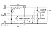
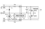
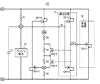
図1及び図2は、本発明の各実施形態に係る静電気保護回路を内蔵する半導体集積回路装置の構成例を示す回路図である。この半導体集積回路装置は、電源端子P1及びP2と、信号端子P3と、ダイオード1及び2と、電源配線3及び4と、静電気保護回路10と、内部回路20とを含んでいる。電源配線3及び4の各々は、抵抗成分を有している。また、内部回路20は、PチャネルMOSトランジスターQP20と、NチャネルMOSトランジスターQN20とを含んでいる。
1 and 2 are circuit diagrams showing a configuration example of a semiconductor integrated circuit device incorporating a static electricity protection circuit according to each embodiment of the present invention. The semiconductor integrated circuit device includes power supply terminals P1 and P2, a signal terminal P3,
図1及び図2においては、一例として、静電気保護回路10が、高電位側の電源電位VDDが供給される電源端子P1にノードN1を介して接続されると共に、低電位側の電源電位VSSが供給される電源端子P2にノードN2を介して接続される場合が示されている。以下、この場合について説明する。
In FIG. 1 and FIG. 2, as an example, the
例えば、静電気の放電によって電源端子P2に正の電荷が印加されると、正の電荷がダイオード2を介して信号端子P3に放出され、又は、ダイオード2及び1を介して電源端子P1に放出されるので、内部回路20に過大な電圧が印加されることがなく、内部回路20の破壊を防止することができる。従って、問題となるのは、ダイオード1及び2の内の少なくとも一方に逆電圧が印加される場合である。
For example, when a positive charge is applied to the power supply terminal P2 due to electrostatic discharge, the positive charge is released to the signal terminal P3 through the
図1には、静電気の放電によって信号端子P3に正の電荷が印加される一方、電源端子P2が接地されている場合の放電経路が示されている。静電気の放電によって、サージ電流IESDが、ダイオード1、電源配線3、静電気保護回路10、及び、電源配線4の経路で流れる。
FIG. 1 shows a discharge path when a positive charge is applied to the signal terminal P3 due to electrostatic discharge while the power supply terminal P2 is grounded. A surge current I ESD flows through a path of the
放電動作において、逆電圧が印加されるダイオード2と並列に接続されたトランジスターQN20のドレイン・ソース間電圧が、トランジスターQN20が破壊に至る電圧VDMGよりも小さければ、静電気保護回路10が内部回路20を保護することができる。そのためには、次式(1)を満たす必要がある。
VF+VW+VPC<VDMG ・・・(1)
ここで、VFはダイオード1の順方向電圧であり、VWは電源配線3の抵抗成分にサージ電流IESDが流れた際に発生する電圧であり、VPCは静電気保護回路10にサージ電流IESDが流れた際に発生する電圧である。
In the discharge operation, if the drain-source voltage of the transistor QN20 connected in parallel with the
V F + V W + V PC <V DMG (1)
Here, V F is the forward voltage of the
また、図2には、静電気の放電によって信号端子P3に負の電荷が印加される一方、電源端子P1が接地されている場合の放電経路が示されている。静電気の放電によって、サージ電流IESDが、電源配線3、静電気保護回路10、電源配線4、及び、ダイオード2の経路で流れる。
Further, FIG. 2 shows a discharge path when a negative charge is applied to the signal terminal P3 due to electrostatic discharge while the power supply terminal P1 is grounded. The surge current I ESD flows through the path of the
放電動作において、逆電圧が印加されるダイオード1と並列に接続されたトランジスターQP20のソース・ドレイン間電圧が、トランジスターQP20が破壊に至る電圧VDMGよりも小さければ、静電気保護回路10が内部回路20を保護することができる。そのためには、次式(2)を満たす必要がある。
VF+VW+VPC<VDMG ・・・(2)
ここで、VFはダイオード2の順方向電圧であり、VWは電源配線4の抵抗成分にサージ電流IESDが流れた際に発生する電圧であり、VPCは静電気保護回路10にサージ電流IESDが流れた際に発生する電圧である。
In the discharge operation, if the voltage between the source and the drain of the transistor QP20 connected in parallel with the
V F + V W + V PC <V DMG (2)
Here, V F is the forward voltage of the
式(1)及び式(2)から分かるように、図1に示す場合と図2に示す場合とにおいて、内部回路20を保護するための条件は、同じ式で表すことができる。即ち、放電経路上のデバイスに発生する電圧の総和が、内部回路20の素子が破壊に至る電圧VDMGよりも小さいことが、内部回路20を保護するための条件となる。
As can be seen from the equations (1) and (2), the conditions for protecting the
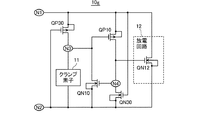
<第1の実施形態>
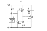
図3は、本発明の第1の実施形態に係る静電気保護回路の構成例を示す回路図である。図3に示すように、静電気保護回路10は、第1及び第2のインピーダンス素子としての抵抗素子R1及びR2と、クランプ素子11と、第1のトランジスターとしてのPチャネルMOSトランジスターQP10と、第2のトランジスターとしてのNチャネルMOSトランジスターQN10と、放電回路12とを含んでいる。
<First Embodiment>
FIG. 3 is a circuit diagram showing a configuration example of the electrostatic protection circuit according to the first embodiment of the present invention. As shown in FIG. 3, the
静電気保護回路10は、高電位側の電位が供給される第1の端子にノードN1を介して接続されると共に、低電位側の電位が供給される第2の端子にノードN2を介して接続される。ノードN3において互いに接続された抵抗素子R1及びクランプ素子11を含む直列回路が、ノードN1とノードN2との間に接続されている。本実施形態においては、抵抗素子R1が、ノードN1とノードN3との間に接続されており、クランプ素子11が、ノードN3とノードN2との間に接続されている。
The
クランプ素子11は、例えば、ダイオードと、ゲートがドレイン又はソースに接続されたPチャネルトランジスター又はNチャネルトランジスターとの内の少なくとも1つを含んでいる。ノードN1とノードN2との間に正の高電圧が印加されると、抵抗素子R1を介してクランプ素子11に電流が流れ、クランプ素子11は、その両端間の電圧を略一定の値(以下においては、「クランプ電圧」ともいう)に保つ。
The
トランジスターQP10は、ノードN1とノードN4との間に接続され、抵抗素子R1に発生する電圧の上昇に従ってオンする。即ち、トランジスターQP10は、ノードN1に接続されたソースと、ノードN4に接続されたドレインと、ノードN3に接続されたゲートとを有しており、ノードN1とノードN3との間の電圧が閾値電圧以上になるとオンする。 The transistor QP10 is connected between the node N1 and the node N4, and is turned on as the voltage generated in the resistance element R1 increases. That is, the transistor QP10 has a source connected to the node N1, a drain connected to the node N4, and a gate connected to the node N3, and the voltage between the node N1 and the node N3 is a threshold value. Turns on when the voltage is exceeded.
抵抗素子R2は、ノードN4とノードN2との間に接続されている。トランジスターQN10は、抵抗素子R2に発生する電圧の上昇に従ってオンし、抵抗素子R1に流れる電流を増加させる。即ち、トランジスターQN10は、ノードN3に接続されたドレインと、ノードN2に接続されたソースと、ノードN4に接続されたゲートとを有しており、ノードN4とノードN2との間の電圧が閾値電圧以上になるとオンする。 Resistance element R2 is connected between nodes N4 and N2. The transistor QN10 is turned on as the voltage generated in the resistance element R2 increases, and increases the current flowing through the resistance element R1. That is, the transistor QN10 has a drain connected to the node N3, a source connected to the node N2, and a gate connected to the node N4, and the voltage between the node N4 and the node N2 is a threshold value. Turns on when the voltage is exceeded.
放電回路12は、例えば、NチャネルMOSトランジスターQN12を含んでいる。トランジスターQN12は、ノードN1に接続されたドレインと、ノードN2に接続されたソースと、ノードN4に接続されたゲートとを有している。放電回路12は、トランジスターQN10がオン状態であるときに、抵抗素子R2に発生する電圧に従って、ノードN1からノードN2に電流を流す。
The
ここで、図3に示す静電気保護回路10の動作について説明する。
通常動作時において、ノードN1とノードN2との間に印加される正の電圧(ノードN1の電位>ノードN2の電位)がクランプ電圧よりも小さい場合には、抵抗素子R1及びクランプ素子11に殆ど電流が流れないので、ノードN1とノードN3との間の電圧がトランジスターQP10の閾値電圧よりも小さいままとなり、トランジスターQP10がオフ状態を維持する。
Here, the operation of the
In a normal operation, when the positive voltage applied between the node N1 and the node N2 (the potential of the node N1> the potential of the node N2) is smaller than the clamp voltage, the resistance element R1 and the
一方、静電気の放電によって、ノードN1とノードN2との間にクランプ電圧以上の電圧が印加されると、ノードN1から抵抗素子R1及びクランプ素子11を介してノードN2に電流が流れる。ノードN1とノードN2との間の電圧がさらに上昇して、ノードN1とノードN3との間の電圧がトランジスターQP10の閾値電圧以上になると、トランジスターQP10がオンすることにより、抵抗素子R2に電流が流れて、ノードN4とノードN2との間の電圧が0Vから上昇する。
On the other hand, when a voltage equal to or higher than the clamp voltage is applied between the node N1 and the node N2 due to electrostatic discharge, a current flows from the node N1 to the node N2 via the resistance element R1 and the
ノードN4とノードN2との間の電圧がトランジスターQN10の閾値電圧以上になると、トランジスターQN10がオンして、抵抗素子R1に流れる電流が増加し、ノードN1とノードN3との間の電圧が上昇するので、トランジスターQP10に流れる電流が増加する(正帰還)。また、ノードN4とノードN2との間の電圧が放電回路12のトランジスターQN12の閾値電圧以上になると、トランジスターQN12が、ノードN1からノードN2に電流を流し始める。
When the voltage between the node N4 and the node N2 becomes equal to or higher than the threshold voltage of the transistor QN10, the transistor QN10 is turned on, the current flowing through the resistance element R1 increases, and the voltage between the node N1 and the node N3 increases. Therefore, the current flowing through the transistor QP10 increases (positive feedback). When the voltage between the node N4 and the node N2 becomes equal to or higher than the threshold voltage of the transistor QN12 of the
トランジスターQP10に流れる電流が増加することにより、抵抗素子R2に流れる電流も増加するので、ノードN4とノードN2との間の電圧が上昇する。その結果、トランジスターQN10に流れる電流が増加して(正帰還)、ノードN3の電位がノードN2の電位まで低下する。同時に、放電回路12のトランジスターQN12に流れる電流も増加する。
As the current flowing through the transistor QP10 increases, the current flowing through the resistance element R2 also increases, so that the voltage between the node N4 and the node N2 rises. As a result, the current flowing through the transistor QN10 increases (positive feedback), and the potential of the node N3 decreases to the potential of the node N2. At the same time, the current flowing through the transistor QN12 of the
放電回路12のトランジスターQN12に電流が流れ続けると、半導体集積回路装置に蓄積された電荷が放電されて、ノードN1とノードN2との間の電圧が低下する。これにより、抵抗素子R1及びR2に流れる電流が減少するので、トランジスターQP10及びQN10のオン抵抗が増加する。
When the current continues to flow through the transistor QN12 of the
ノードN1とノードN3との間の電圧がトランジスターQP10の閾値電圧よりも小さくなると、トランジスターQP10がオフする。また、ノードN4とノードN2との間の電圧がトランジスターQN10の閾値電圧よりも小さくなると、トランジスターQN10がオフする。同様に、ノードN4とノードN2との間の電圧が放電回路12のトランジスターQN12の閾値電圧よりも小さくなると、トランジスターQN12がオフする。
When the voltage between the node N1 and the node N3 becomes smaller than the threshold voltage of the transistor QP10, the transistor QP10 is turned off. Further, when the voltage between the node N4 and the node N2 becomes lower than the threshold voltage of the transistor QN10, the transistor QN10 is turned off. Similarly, when the voltage between the node N4 and the node N2 becomes smaller than the threshold voltage of the transistor QN12 of the
このように、トランジスターQP10及びQN10がオフ状態からオン状態に遷移する際には、ノードN1とノードN2との間の電圧が動作開始電圧以上であるか否かによって遷移条件が決定される。ここで、動作開始電圧は、クランプ素子11のクランプ電圧とトランジスターQP10の閾値電圧との和になる。一方、トランジスターQP10及びQN10が一旦オン状態になると、ノードN1とノードN2との間の電圧が動作開始電圧より小さくなっても、トランジスターQP10及びQN10がオン状態を保ち続ける。
Thus, when the transistors QP10 and QN10 transition from the off state to the on state, the transition condition is determined depending on whether or not the voltage between the node N1 and the node N2 is equal to or higher than the operation start voltage. Here, the operation start voltage is the sum of the clamp voltage of the
従って、通常使用時に電源投入によって電源電圧が急峻に立ち上がっても、ノードN1とノードN2との間の電圧が動作開始電圧よりも小さければ、静電気保護回路10が保護動作を開始するおそれがない。また、静電気の放電により静電気保護回路10が保護動作を一旦開始すると、ノードN1とノードN2との間の電圧が十分小さくなるまで、静電気保護回路10が保護動作を継続する。このように、本実施形態によれば、簡単な回路構成で、通常動作時において誤動作することなく、静電気の放電に対して十分な保護特性が得られる静電気保護回路10を提供することができる。
Therefore, even if the power supply voltage rises sharply when the power is turned on during normal use, if the voltage between the node N1 and the node N2 is smaller than the operation start voltage, there is no possibility that the
<第2の実施形態>
図4は、本発明の第2の実施形態に係る静電気保護回路の構成例を示す回路図である。第2の実施形態に係る静電気保護回路10aにおいては、図3に示す第1の実施形態に係る静電気保護回路10における放電回路12の替りに、放電回路12aが用いられる。その他の点に関し、図4に示す静電気保護回路10aは、図3に示す静電気保護回路10と同様である。
<Second Embodiment>
FIG. 4 is a circuit diagram showing a configuration example of the electrostatic protection circuit according to the second embodiment of the present invention. In the
放電回路12aは、例えば、PチャネルMOSトランジスターQP12を含んでいる。トランジスターQP12は、ノードN1に接続されたソースと、ノードN2に接続されたドレインと、ノードN3に接続されたゲートとを有している。放電回路12aは、トランジスターQN10がオン状態であるときに、抵抗素子R1に発生する電圧に従って、ノードN1からノードN2に電流を流す。
The
ここで、図4に示す静電気保護回路10aの動作について説明する。
通常動作時において、ノードN1とノードN2との間に印加される正の電圧(ノードN1の電位>ノードN2の電位)がクランプ電圧よりも小さい場合には、抵抗素子R1及びクランプ素子11に殆ど電流が流れないので、ノードN1とノードN3との間の電圧がトランジスターQP10の閾値電圧よりも小さいままとなり、トランジスターQP10がオフ状態を維持する。
Here, the operation of the
In a normal operation, when the positive voltage applied between the node N1 and the node N2 (the potential of the node N1> the potential of the node N2) is smaller than the clamp voltage, the resistance element R1 and the
一方、静電気の放電によって、ノードN1とノードN2との間にクランプ電圧以上の電圧が印加されると、ノードN1から抵抗素子R1及びクランプ素子11を介してノードN2に電流が流れる。ノードN1とノードN2との間の電圧がさらに上昇して、ノードN1とノードN3との間の電圧がトランジスターQP10の閾値電圧以上になると、トランジスターQP10がオンすることにより、抵抗素子R2に電流が流れて、ノードN4とノードN2との間の電圧が0Vから上昇する。
On the other hand, when a voltage equal to or higher than the clamp voltage is applied between the node N1 and the node N2 due to electrostatic discharge, a current flows from the node N1 to the node N2 via the resistance element R1 and the
ノードN4とノードN2との間の電圧がトランジスターQN10の閾値電圧以上になると、トランジスターQN10がオンして、抵抗素子R1に流れる電流が増加し、ノードN1とノードN3との間の電圧が上昇するので、トランジスターQP10に流れる電流が増加する(正帰還)。また、ノードN1とノードN3との間の電圧が放電回路12aのトランジスターQP12の閾値電圧以上になると、トランジスターQP12が、ノードN1からノードN2に電流を流し始める。
When the voltage between the node N4 and the node N2 becomes equal to or higher than the threshold voltage of the transistor QN10, the transistor QN10 is turned on, the current flowing through the resistance element R1 increases, and the voltage between the node N1 and the node N3 increases. Therefore, the current flowing through the transistor QP10 increases (positive feedback). When the voltage between the node N1 and the node N3 becomes equal to or higher than the threshold voltage of the transistor QP12 of the
トランジスターQP10に流れる電流が増加することにより、抵抗素子R2に流れる電流も増加するので、ノードN4とノードN2との間の電圧が上昇する。その結果、トランジスターQN10に流れる電流が増加して(正帰還)、ノードN3の電位がノードN2の電位まで低下する。同時に、放電回路12aのトランジスターQP12に流れる電流も増加する。
As the current flowing through the transistor QP10 increases, the current flowing through the resistance element R2 also increases, so that the voltage between the node N4 and the node N2 rises. As a result, the current flowing through the transistor QN10 increases (positive feedback), and the potential of the node N3 decreases to the potential of the node N2. At the same time, the current flowing through the transistor QP12 of the
放電回路12aのトランジスターQP12に電流が流れ続けると、半導体集積回路装置に蓄積された電荷が放電されて、ノードN1とノードN2との間の電圧が低下する。これにより、抵抗素子R1及びR2に流れる電流が減少するので、トランジスターQP10及びQN10のオン抵抗が増加する。
When the current continues to flow through the transistor QP12 of the
ノードN1とノードN3との間の電圧がトランジスターQP10の閾値電圧よりも小さくなると、トランジスターQP10がオフする。また、ノードN4とノードN2との間の電圧がトランジスターQN10の閾値電圧よりも小さくなると、トランジスターQN10がオフする。同様に、ノードN1とノードN3との間の電圧が放電回路12aのトランジスターQP12の閾値電圧よりも小さくなると、トランジスターQP12がオフする。
When the voltage between the node N1 and the node N3 becomes smaller than the threshold voltage of the transistor QP10, the transistor QP10 is turned off. Further, when the voltage between the node N4 and the node N2 becomes lower than the threshold voltage of the transistor QN10, the transistor QN10 is turned off. Similarly, when the voltage between the node N1 and the node N3 becomes smaller than the threshold voltage of the transistor QP12 of the
このように、トランジスターQP10及びQN10がオフ状態からオン状態に遷移する際には、ノードN1とノードN2との間の電圧が動作開始電圧以上であるか否かによって遷移条件が決定される。ここで、動作開始電圧は、クランプ素子11のクランプ電圧とトランジスターQP10の閾値電圧との和になる。一方、トランジスターQP10及びQN10が一旦オン状態になると、ノードN1とノードN2との間の電圧が動作開始電圧より小さくなっても、トランジスターQP10及びQN10がオン状態を保ち続ける。
Thus, when the transistors QP10 and QN10 transition from the off state to the on state, the transition condition is determined depending on whether or not the voltage between the node N1 and the node N2 is equal to or higher than the operation start voltage. Here, the operation start voltage is the sum of the clamp voltage of the
従って、通常使用時に電源投入によって電源電圧が急峻に立ち上がっても、ノードN1とノードN2との間の電圧が動作開始電圧よりも小さければ、静電気保護回路10aが保護動作を開始するおそれがない。また、静電気の放電により静電気保護回路10aが保護動作を一旦開始すると、ノードN1とノードN2との間の電圧が十分小さくなるまで、静電気保護回路10aが保護動作を継続する。このように、本実施形態によれば、簡単な回路構成で、通常動作時において誤動作することなく、静電気の放電に対して十分な保護特性が得られる静電気保護回路10aを提供することができる。
Therefore, even if the power supply voltage rises sharply when the power is turned on during normal use, if the voltage between the node N1 and the node N2 is smaller than the operation start voltage, there is no possibility that the
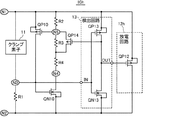
<第3の実施形態>
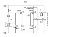
図5は、本発明の第3の実施形態に係る静電気保護回路の構成例を示す回路図である。第3の実施形態に係る静電気保護回路10bにおいては、図3に示す第1の実施形態に係る静電気保護回路10に対して、検出回路13が追加されている。その他の点に関し、図5に示す静電気保護回路10bは、図3に示す静電気保護回路10と同様である。
<Third Embodiment>
FIG. 5 is a circuit diagram showing a configuration example of an electrostatic protection circuit according to the third embodiment of the present invention. In the
検出回路13は、トランジスターQN10がオン状態であることを検出したときに出力信号を活性化する。例えば、検出回路13は、PチャネルMOSトランジスターQP13とNチャネルMOSトランジスターQN13とによって構成されるインバーターを含んでいる。トランジスターQP13は、ノードN1に接続されたソースと、出力端子OUTに接続されたドレインと、入力端子INに接続されたゲートとを有している。また、トランジスターQN13は、出力端子OUTに接続されたドレインと、ノードN2に接続されたソースと、入力端子INに接続されたゲートとを有している。
The
インバーターは、入力端子INに供給されるノードN3の電位がハイレベルであるかローレベルであるかを検出し、そのレベルを反転して、反転されたレベルを有する出力信号を出力端子OUTから出力する。これにより、検出回路13は、抵抗素子R1に発生する電圧がノードN1とノードN2との間の電圧に対して所定の割合(例えば、50%)よりも大きくなったときに出力信号をハイレベルに活性化する。検出回路13としては、インバーター以外にも、コンパレーター等を用いることができる。
The inverter detects whether the potential of the node N3 supplied to the input terminal IN is high level or low level, inverts the level, and outputs an output signal having the inverted level from the output terminal OUT To do. Thereby, the
検出回路13の出力信号は、放電回路12のトランジスターQN12のゲートに供給される。放電回路12は、トランジスターQN10がオン状態となって、検出回路13の出力信号がハイレベルに活性化されたときに、ノードN1からノードN2に電流を流す。
The output signal of the
ここで、図5に示す静電気保護回路10bの動作について説明する。
通常動作時において、ノードN1とノードN2との間に印加される正の電圧(ノードN1の電位>ノードN2の電位)がクランプ電圧よりも小さい場合には、抵抗素子R1及びクランプ素子11に殆ど電流が流れないので、ノードN1とノードN3との間の電圧がトランジスターQP10の閾値電圧よりも小さいままとなり、トランジスターQP10がオフ状態を維持する。
Here, the operation of the
In a normal operation, when the positive voltage applied between the node N1 and the node N2 (the potential of the node N1> the potential of the node N2) is smaller than the clamp voltage, the resistance element R1 and the
一方、静電気の放電によって、ノードN1とノードN2との間にクランプ電圧以上の電圧が印加されると、ノードN1から抵抗素子R1及びクランプ素子11を介してノードN2に電流が流れる。ノードN1とノードN2との間の電圧がさらに上昇して、ノードN1とノードN3との間の電圧がトランジスターQP10の閾値電圧以上になると、トランジスターQP10がオンする。ただし、この時点においては、検出回路13の入力端子INの電位はハイレベルとなっている。
On the other hand, when a voltage equal to or higher than the clamp voltage is applied between the node N1 and the node N2 due to electrostatic discharge, a current flows from the node N1 to the node N2 via the resistance element R1 and the
トランジスターQP10がオンすることにより、抵抗素子R2に電流が流れて、ノードN4とノードN2との間の電圧が0Vから上昇する。ノードN4とノードN2との間の電圧がトランジスターQN10の閾値電圧以上になると、トランジスターQN10がオンする。 When the transistor QP10 is turned on, a current flows through the resistance element R2, and the voltage between the node N4 and the node N2 rises from 0V. When the voltage between the node N4 and the node N2 becomes equal to or higher than the threshold voltage of the transistor QN10, the transistor QN10 is turned on.
トランジスターQN10がオンすることにより、抵抗素子R1に流れる電流が増加して、ノードN1とノードN3との間の電圧が上昇するので、トランジスターQP10に流れる電流が増加する(正帰還)。同時に、検出回路13の入力端子INの電位がローレベルとなり、検出回路13の出力信号がハイレベルに活性化される。これにより、放電回路12のトランジスターQN12が、ノードN1からノードN2に電流を流し始める。
When the transistor QN10 is turned on, the current flowing through the resistance element R1 increases and the voltage between the node N1 and the node N3 increases, so that the current flowing through the transistor QP10 increases (positive feedback). At the same time, the potential of the input terminal IN of the
また、トランジスターQP10に流れる電流が増加することにより、抵抗素子R2に流れる電流が増加する。その結果、ノードN4とノードN2との間の電圧が上昇するので、トランジスターQN10に流れる電流が増加する(正帰還)。同時に、放電回路12のトランジスターQN12に流れる電流も増加する。
Further, as the current flowing through the transistor QP10 increases, the current flowing through the resistance element R2 increases. As a result, the voltage between the node N4 and the node N2 increases, so that the current flowing through the transistor QN10 increases (positive feedback). At the same time, the current flowing through the transistor QN12 of the
放電回路12のトランジスターQN12に電流が流れ続けると、半導体集積回路装置に蓄積された電荷が放電されて、ノードN1とノードN2との間の電圧が低下する。これにより、抵抗素子R1及びR2に流れる電流が減少するので、トランジスターQP10及びQN10のオン抵抗が増加する。
When the current continues to flow through the transistor QN12 of the
ノードN1とノードN3との間の電圧がトランジスターQP10の閾値電圧よりも小さくなると、トランジスターQP10がオフする。また、ノードN4とノードN2との間の電圧がトランジスターQN10の閾値電圧よりも小さくなると、トランジスターQN10がオフする。これにより、検出回路13の出力信号がローレベルに非活性化されて、放電回路12のトランジスターQN12がオン状態からオフ状態に遷移する。
When the voltage between the node N1 and the node N3 becomes smaller than the threshold voltage of the transistor QP10, the transistor QP10 is turned off. Further, when the voltage between the node N4 and the node N2 becomes lower than the threshold voltage of the transistor QN10, the transistor QN10 is turned off. As a result, the output signal of the
このように、トランジスターQP10及びQN10がオフ状態からオン状態に遷移する際には、ノードN1とノードN2との間の電圧が動作開始電圧以上であるか否かによって遷移条件が決定される。ここで、動作開始電圧は、クランプ素子11のクランプ電圧とトランジスターQP10の閾値電圧との和になる。一方、トランジスターQP10及びQN10が一旦オン状態になると、ノードN1とノードN2との間の電圧が動作開始電圧より小さくなっても、トランジスターQP10及びQN10がオン状態を保ち続ける。
Thus, when the transistors QP10 and QN10 transition from the off state to the on state, the transition condition is determined depending on whether or not the voltage between the node N1 and the node N2 is equal to or higher than the operation start voltage. Here, the operation start voltage is the sum of the clamp voltage of the
従って、通常使用時に電源投入によって電源電圧が急峻に立ち上がっても、ノードN1とノードN2との間の電圧が動作開始電圧よりも小さければ、静電気保護回路10bが保護動作を開始するおそれがない。また、静電気の放電により静電気保護回路10bが保護動作を一旦開始すると、ノードN1とノードN2との間の電圧が十分小さくなるまで、静電気保護回路10bが保護動作を継続する。このように、本実施形態によれば、簡単な回路構成で、通常動作時において誤動作することなく、静電気の放電に対して十分な保護特性が得られる静電気保護回路10bを提供することができる。
Therefore, even if the power supply voltage rises sharply when the power is turned on during normal use, if the voltage between the node N1 and the node N2 is smaller than the operation start voltage, there is no possibility that the
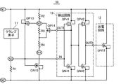
<第4の実施形態>
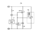
図6は、本発明の第4の実施形態に係る静電気保護回路の構成例を示す回路図である。第4の実施形態に係る静電気保護回路10cは、図5に示す第3の実施形態に係る静電気保護回路10bに対して抵抗素子R3が追加されている。その他の点に関し、図6に示す静電気保護回路10cは、図5に示す静電気保護回路10bと同様である。
<Fourth Embodiment>
FIG. 6 is a circuit diagram showing a configuration example of an electrostatic protection circuit according to the fourth embodiment of the present invention. In the
抵抗素子R3は、ノードN4とノードN5との間に接続されている。また、抵抗素子R2は、ノードN5とノードN2との間に接続されている。ここで、抵抗素子R3及びR2は、ノードN4とノードN2との間の電圧を分圧する分圧回路を構成している。 Resistance element R3 is connected between nodes N4 and N5. The resistance element R2 is connected between the node N5 and the node N2. Here, the resistance elements R3 and R2 constitute a voltage dividing circuit that divides the voltage between the node N4 and the node N2.
トランジスターQN10は、分圧回路によって分圧された電圧の上昇に従ってオンし、抵抗素子R1に流れる電流を増加させる。即ち、トランジスターQN10は、ノードN3に接続されたドレインと、ノードN2に接続されたソースと、ノードN5に接続されたゲートとを有しており、ノードN5とノードN2との間の電圧が閾値電圧以上になるとオンする。 The transistor QN10 is turned on as the voltage divided by the voltage dividing circuit increases, and increases the current flowing through the resistance element R1. That is, the transistor QN10 has a drain connected to the node N3, a source connected to the node N2, and a gate connected to the node N5, and the voltage between the node N5 and the node N2 is a threshold value. Turns on when the voltage is exceeded.
ここで、図6に示す静電気保護回路10cの動作について説明する。
通常動作時において、ノードN1とノードN2との間に印加される正の電圧(ノードN1の電位>ノードN2の電位)がクランプ電圧よりも小さい場合には、抵抗素子R1及びクランプ素子11に殆ど電流が流れないので、ノードN1とノードN3との間の電圧がトランジスターQP10の閾値電圧よりも小さいままとなり、トランジスターQP10がオフ状態を維持する。
Here, the operation of the
In a normal operation, when the positive voltage applied between the node N1 and the node N2 (the potential of the node N1> the potential of the node N2) is smaller than the clamp voltage, the resistance element R1 and the
一方、静電気の放電によって、ノードN1とノードN2との間にクランプ電圧以上の電圧が印加されると、ノードN1から抵抗素子R1及びクランプ素子11を介してノードN2に電流が流れる。ノードN1とノードN2との間の電圧がさらに上昇して、ノードN1とノードN3との間の電圧がトランジスターQP10の閾値電圧以上になると、トランジスターQP10がオンする。ただし、この時点においては、検出回路13の入力端子INの電位はハイレベルとなっている。
On the other hand, when a voltage equal to or higher than the clamp voltage is applied between the node N1 and the node N2 due to electrostatic discharge, a current flows from the node N1 to the node N2 via the resistance element R1 and the
トランジスターQP10がオンすることにより、抵抗素子R3及びR2によって構成される分圧回路に電圧が印加されて、ノードN5とノードN2との間の電圧が0Vから上昇する。ここで、ノードN1とノードN2との間の電圧が所定の値以上であれば、ノードN5とノードN2との間の電圧がトランジスターQN10の閾値電圧以上になって、トランジスターQN10がオンする。 When the transistor QP10 is turned on, a voltage is applied to the voltage dividing circuit constituted by the resistance elements R3 and R2, and the voltage between the node N5 and the node N2 rises from 0V. If the voltage between the node N1 and the node N2 is equal to or higher than a predetermined value, the voltage between the node N5 and the node N2 becomes equal to or higher than the threshold voltage of the transistor QN10, and the transistor QN10 is turned on.
トランジスターQN10がオンすることにより、抵抗素子R1に流れる電流が増加して、ノードN1とノードN3との間の電圧が上昇するので、トランジスターQP10に流れる電流が増加する(正帰還)。同時に、検出回路13の入力端子INの電位がローレベルとなり、検出回路13の出力信号がハイレベルに活性化される。これにより、放電回路12のトランジスターQN12が、ノードN1からノードN2に電流を流し始める。
When the transistor QN10 is turned on, the current flowing through the resistance element R1 increases and the voltage between the node N1 and the node N3 increases, so that the current flowing through the transistor QP10 increases (positive feedback). At the same time, the potential of the input terminal IN of the
また、トランジスターQP10に流れる電流が増加することにより、抵抗素子R3及びR2に流れる電流が増加する。その結果、ノードN5とノードN2との間の電圧が上昇するので、トランジスターQN10に流れる電流が増加する(正帰還)。同時に、放電回路12のトランジスターQN12に流れる電流も増加する。
Further, as the current flowing through the transistor QP10 increases, the current flowing through the resistance elements R3 and R2 increases. As a result, since the voltage between the node N5 and the node N2 increases, the current flowing through the transistor QN10 increases (positive feedback). At the same time, the current flowing through the transistor QN12 of the
放電回路12のトランジスターQN12に流れる電流が増加すると、ノードN1とノードN2との間の電圧が所定の値よりも低下する。これにより、ノードN5とノードN2との間の電圧がトランジスターQN10の閾値電圧よりも低下するので、トランジスターQN10がオン状態からオフ状態に遷移する。その結果、抵抗素子R1に流れる電流が減少するので、検出回路13の出力信号がローレベルに非活性化され、放電回路12のトランジスターQN12がオン状態からオフ状態に遷移して、ノードN1とノードN2との間の電圧が略一定に保持される。
When the current flowing through the transistor QN12 of the
このように、トランジスターQP10及びQN10がオフ状態からオン状態に遷移する際には、ノードN1とノードN2との間の電圧が動作開始電圧以上であるか否かによって遷移条件が決定される。ここで、動作開始電圧は、クランプ素子11のクランプ電圧とトランジスターQP10の閾値電圧との和になる。一方、トランジスターQP10及びQN10が一旦オン状態になると、ノードN1とノードN2との間の電圧が動作開始電圧より小さくなっても、トランジスターQP10及びQN10がオン状態を保ち続ける。
Thus, when the transistors QP10 and QN10 transition from the off state to the on state, the transition condition is determined depending on whether or not the voltage between the node N1 and the node N2 is equal to or higher than the operation start voltage. Here, the operation start voltage is the sum of the clamp voltage of the
従って、通常使用時に電源投入によって電源電圧が急峻に立ち上がっても、ノードN1とノードN2との間の電圧が動作開始電圧よりも小さければ、静電気保護回路10cが保護動作を開始するおそれがない。また、静電気の放電により静電気保護回路10cが保護動作を一旦開始すると、ノードN1とノードN2との間の電圧が所定の値に減少するまで、静電気保護回路10cが保護動作を継続する。このように、本実施形態によれば、静電気の放電により静電気保護回路10cが保護動作を行っている間において、ノードN1とノードN2との間の電圧を所定の値に保持することができる。
Therefore, even if the power supply voltage rises sharply when the power is turned on during normal use, if the voltage between the node N1 and the node N2 is smaller than the operation start voltage, there is no possibility that the
以上の動作メカニズムにより、静電気保護回路10cの両端間の電圧が所定の値に保持されながら、放電経路に電流が流れる。以下においては、静電気保護回路10cの両端間に保持される電圧を「保持電圧」ともいう。本実施形態においては、保持電圧が略一定値となる。
With the above operation mechanism, a current flows through the discharge path while the voltage across the
保持電圧VHは、トランジスターQN10がオン状態からオフ状態に遷移するときのノードN1とノードN2との間の電圧であり、次式(3)によって近似できる。
VH≒VthQN10×(R2+R3)/R2 ・・・(3)
ここで、VthQN10はトランジスターQN10の閾値電圧であり、R2は抵抗素子R2の抵抗値であり、R3は抵抗素子R3の抵抗値である。ただし、抵抗値R2及びR3は、トランジスターQP10のオン抵抗よりも十分大きい値であるものとする。式(3)に従って抵抗素子R2及びR3の抵抗値を選択することにより、所望の保持電圧VHを設定することができる。
The holding voltage V H is a voltage between the node N1 and the node N2 when the transistor QN10 transitions from the on state to the off state, and can be approximated by the following equation (3).
V H ≈Vth QN10 × (R 2 + R 3 ) / R 2 (3)
Here, Vth QN10 is the threshold voltage of the transistor QN10, R 2 is the resistance value of the resistance element R2, R 3 is a resistance of the resistor R3. However, it is assumed that the resistance values R 2 and R 3 are sufficiently larger than the on-resistance of the transistor QP10. By selecting the resistance value of the resistance element R2 and R3 according to formula (3), it is possible to set a desired holding voltage V H.
第1又は第2のインピーダンス素子として抵抗素子を用いる場合には、抵抗素子の抵抗値が一定であるので、トランジスターQP10又はQN10のオン条件の設定が容易になる。インピーダンス素子として抵抗素子以外のデバイスを用いることも可能であるが、それについては後で詳しく説明する。 When a resistance element is used as the first or second impedance element, since the resistance value of the resistance element is constant, it is easy to set the ON condition of the transistor QP10 or QN10. It is possible to use a device other than the resistance element as the impedance element, which will be described in detail later.
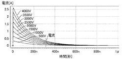
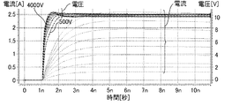
図7は、ヒューマンボディモデルにおける静電気放電の電流波形を示す図である。図7において、横軸は、時間[秒]を表しており、縦軸は、電流[A]を表している。例えば、2000Vの静電気が人体から半導体集積回路装置に印加された場合には、ピーク電流が約1.3Aとなり、約1μ秒の期間においてサージ電流が流れ続ける。 FIG. 7 is a diagram showing a current waveform of electrostatic discharge in the human body model. In FIG. 7, the horizontal axis represents time [seconds], and the vertical axis represents current [A]. For example, when 2000V static electricity is applied from the human body to the semiconductor integrated circuit device, the peak current is about 1.3 A, and the surge current continues to flow for a period of about 1 μsec.
図8及び図9は、図7に示すヒューマンボディモデルを適用した場合の図6に示す静電気保護回路における電流波形及び電圧波形のシミュレーション結果を示す図である。一方、図10及び図11は、図7に示すヒューマンボディモデルを適用した場合の比較例の静電気保護回路における電流波形及び電圧波形のシミュレーション結果を示す図である。図8〜図11において、横軸は、時間[秒]を表しており、縦軸は、電流[A]又は電圧[V]を表している。 8 and 9 are diagrams showing simulation results of current waveforms and voltage waveforms in the electrostatic protection circuit shown in FIG. 6 when the human body model shown in FIG. 7 is applied. On the other hand, FIGS. 10 and 11 are diagrams showing simulation results of current waveforms and voltage waveforms in the electrostatic protection circuit of the comparative example when the human body model shown in FIG. 7 is applied. 8 to 11, the horizontal axis represents time [second], and the vertical axis represents current [A] or voltage [V].
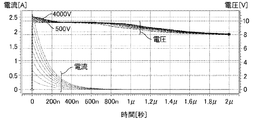
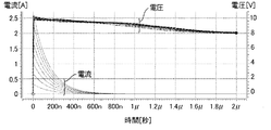
比較例の静電気保護回路は、図6に示す静電気保護回路10cにおいて、クランプ素子11の替りにキャパシターを用いたものである。また、図6に示す静電気保護回路10c及び比較例の静電気保護回路において、保持電圧は約10Vに設定されている。図8に示すように、静電気保護回路10cは、電流が流れている期間において、約10Vの電圧を保持し続けている。図10に示す比較例の静電気保護回路の保持電圧も、ほぼ同様に見える。
The electrostatic protection circuit of the comparative example uses a capacitor in place of the
図9及び図11は、図8及び図10の時間軸における0〜10n秒の期間を拡大して示している。図11に示すように、比較例の静電気保護回路においては、短い期間ではあるが、保持電圧が約10Vよりも降下している。これは、急峻なESDイベントに対し、静電気保護回路が確実にサージ電流を逃がしていることを示す一方、通常動作時において外部からノイズ等を受けた場合には、静電気保護回路が過剰に動作して電源電圧が落ちるおそれがあることを意味している。 9 and 11 show an enlarged period of 0 to 10 ns on the time axis of FIGS. 8 and 10. As shown in FIG. 11, in the electrostatic protection circuit of the comparative example, the holding voltage drops below about 10 V for a short period. This indicates that the ESD protection circuit is surely releasing the surge current against a sudden ESD event. On the other hand, if it receives external noise during normal operation, the ESD protection circuit will operate excessively. This means that the power supply voltage may drop.
通常動作時において電源電圧が落ちると、半導体集積回路装置が誤動作するおそれがある。そこで、比較例の静電気保護回路において、通常動作時における誤動作を回避するために、キャパシターの容量値を小さくすることも考えられる。しかしながら、キャパシターの容量値を小さくし過ぎると保護機能が低下する可能性があり、低周波のノイズに対して静電気保護回路が保護動作を行わない可能性が生じる。 If the power supply voltage drops during normal operation, the semiconductor integrated circuit device may malfunction. Therefore, in the electrostatic protection circuit of the comparative example, it is conceivable to reduce the capacitance value of the capacitor in order to avoid malfunction during normal operation. However, if the capacitance value of the capacitor is too small, the protection function may be reduced, and the electrostatic protection circuit may not perform a protection operation against low-frequency noise.
一方、図9に示すように、図6に示す静電気保護回路10cにおいては、保持電圧が降下することなく放電動作が行われている。これは、通常動作時において外部からノイズ等を受けた場合においても、静電気保護回路10cが過剰に動作して電源電圧が落ちるおそれがないことを意味している。また、クランプ素子11は、印加される電圧がクランプ電圧に達すると動作を開始するので、低周波のノイズに対しても確実に保護動作を行うことができる。
On the other hand, as shown in FIG. 9, in the
<第5の実施形態>
図12は、本発明の第5の実施形態に係る静電気保護回路の構成例を示す回路図である。第5の実施形態に係る静電気保護回路10dは、図6に示す第4の実施形態に係る静電気保護回路10cに対してキャパシターC1が追加されている。その他の点に関し、図12に示す静電気保護回路10dは、図6に示す静電気保護回路10cと同様である。
<Fifth Embodiment>
FIG. 12 is a circuit diagram showing a configuration example of an electrostatic protection circuit according to the fifth embodiment of the present invention. In the
キャパシターC1は、複数の配線層にそれぞれ形成された複数の電極を用いて構成されても良いし、少なくとも1つのMOSトランジスターを用いて構成されても良い。例えば、NチャネルMOSトランジスターのドレイン、ソース、及び、バックゲートを第1の電極とし、ゲートを第2の電極とすることにより、キャパシターC1を構成することができる。 The capacitor C1 may be configured using a plurality of electrodes respectively formed on a plurality of wiring layers, or may be configured using at least one MOS transistor. For example, the capacitor C1 can be formed by using the drain, source, and back gate of an N-channel MOS transistor as the first electrode and the gate as the second electrode.
図12に示すように、キャパシターC1は、ノードN3とノードN2との間に、クランプ素子11と並列に接続される。これにより、ノードN1とノードN2との間に正の電圧(ノードN1の電位>ノードN2の電位)が印加されると、抵抗素子R1とキャパシターC1との時定数に従って、ノードN1から抵抗素子R1及びキャパシターC1を介してノードN2に電流が流れ、キャパシターC1の充電が行われる。
As shown in FIG. 12, the capacitor C1 is connected in parallel with the
これにより、ノードN1とノードN2との間に印加される電圧がクランプ素子11のクランプ電圧より小さくても、ノードN3の電位は、抵抗素子R1とキャパシターC1との時定数に従って、ノードN2の電位に対して上昇する。ノードN1とノードN2との間に印加される電圧が急峻に上昇する場合には、ノードN1とノードN3との間の電圧がトランジスターQP10の閾値電圧以上となり、トランジスターQP10がオンする。
Thereby, even if the voltage applied between the node N1 and the node N2 is smaller than the clamp voltage of the
本実施形態によれば、急峻なESDイベントに対して静電気保護回路10dが迅速に保護動作を開始するので、確実にサージ電流を逃がすことができる。また、低い周波数のノイズ等で電源電圧が上昇しても、静電気保護回路10dが確実に保護動作を開始して、電源電圧の上昇を抑えることができる。一方、キャパシターC1は、ノイズフィルターとしても機能するので、通常動作時において外部からノイズ等を受けた場合でも、静電気保護回路10dが過剰に動作して電源電圧が落ちることがない。
According to the present embodiment, since the
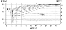
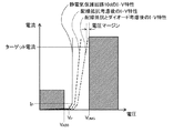
図13は、図1に示す半導体集積回路装置に図12に示す静電気保護回路を適用した場合のI−V特性を示す図であり、図14は、図1に示す半導体集積回路装置に従来の静電気保護回路を適用した場合のI−V特性を示す図である。図13及び図14において、横軸は、放電経路における静電気保護回路等の両端間の電圧を表しており、縦軸は、放電経路に流れる電流を表している。 FIG. 13 is a diagram showing IV characteristics when the electrostatic protection circuit shown in FIG. 12 is applied to the semiconductor integrated circuit device shown in FIG. 1, and FIG. 14 shows a conventional circuit for the semiconductor integrated circuit device shown in FIG. It is a figure which shows the IV characteristic at the time of applying an electrostatic protection circuit. 13 and 14, the horizontal axis represents the voltage across the electrostatic protection circuit in the discharge path, and the vertical axis represents the current flowing through the discharge path.
図13に示すように、本発明の第5の実施形態に係る静電気保護回路10dは、両端間の電圧が絶対最大定格電圧VABS以下の領域においては動作しないので、放電経路に電流が流れない。一方、両端間の電圧が所定の電圧VPを超えると、静電気保護回路10dが動作を開始して、放電経路に電流が流れ始める。放電経路に流れる電流が所定の電流IPを超えると、静電気保護回路10dが両端間の電圧を略一定値に保つ。配線抵抗やダイオードに発生する電圧を考慮しても、放電経路に流れる電流がターゲット電流に達したときに、半導体集積回路装置の端子間の電圧と内部回路20の素子が破壊に至る電圧VDMGとの間には、電圧マージンが存在する。
As shown in FIG. 13, the
一方、特許文献1の図1に示されている従来の静電気保護回路の場合には、図14に示すように、静電気保護回路の両端間の電圧が絶対最大定格電圧VABSよりも低い領域において静電気保護回路が保護動作を開始して、放電経路に電流が流れ始めている。これでは、通常動作時においても、電源投入による電源電圧の急峻な立ち上がりによって静電気保護回路が保護動作を開始して電流が流れ、半導体集積回路装置が誤動作する可能性がある。従って、従来の静電気保護回路を用いる場合には、電源投入時における電源電圧の立ち上がり特性に制限を設ける必要がある。
On the other hand, in the case of the conventional electrostatic protection circuit shown in FIG. 1 of
<第6の実施形態>
図15は、本発明の第6の実施形態に係る静電気保護回路の構成例を示す回路図である。第6の実施形態に係る静電気保護回路10eは、図6に示す第4の実施形態に係る静電気保護回路10cに対して、抵抗素子R3と並列に接続された第3のトランジスターとしてNチャネルMOSトランジスターQN14が追加されており、抵抗素子R4及び/又はキャパシターC1をさらに含んでも良い。その他の点に関し、図15に示す静電気保護回路10eは、図6に示す静電気保護回路10cと同様である。
<Sixth Embodiment>
FIG. 15 is a circuit diagram showing a configuration example of an electrostatic protection circuit according to the sixth embodiment of the present invention. The
トランジスターQN14は、抵抗素子R3の一端に接続されたドレインと、抵抗素子R3の他端に接続されたソースと、検出回路13の出力端子OUTに接続されたゲートとを有し、検出回路13の出力信号がハイレベルに活性化されたときにオンする。また、抵抗素子R4は、ノードN4とノードN5との間に、抵抗素子R3と直列に接続されている。
The transistor QN14 has a drain connected to one end of the resistance element R3, a source connected to the other end of the resistance element R3, and a gate connected to the output terminal OUT of the
トランジスターQN14は、抵抗素子R2〜R4と共に、分圧回路を構成している。静電気の放電により、検出回路13の出力信号がハイレベルに活性化されて、静電気保護回路10eが保護動作を一旦開始すると、トランジスターQN14がオンして、分圧回路における分圧比が上昇する。その結果、ノードN1とノードN2との間の電圧が低下し、半導体集積回路装置の内部回路が破壊に至る電圧に対するマージンが増えて静電気耐量が向上する。
The transistor QN14 forms a voltage dividing circuit together with the resistance elements R2 to R4. Due to the discharge of static electricity, the output signal of the
保持電圧VHは、トランジスターQN10がオン状態からオフ状態に遷移するときのノードN1とノードN2との間の電圧であり、次式(4)によって近似できる。
VH≒VthQN10×(R2+αR3+R4)/R2 ・・・(4)
ここで、VthQN10はトランジスターQN10の閾値電圧であり、αは0〜1の範囲内の係数であり、R2は抵抗素子R2の抵抗値であり、R3は抵抗素子R3の抵抗値であり、R4は抵抗素子R4の抵抗値である。ただし、抵抗値R2及びR3は、トランジスターQP10のオン抵抗よりも十分大きい値であるものとする。また、抵抗素子R4を設けない場合には、R4=0となる。
The holding voltage V H is a voltage between the node N1 and the node N2 when the transistor QN10 transitions from the on state to the off state, and can be approximated by the following equation (4).
V H ≈Vth QN10 × (R 2 + αR 3 + R 4 ) / R 2 (4)
Here, Vth QN10 is the threshold voltage of the transistor QN10, alpha is a coefficient within a range of 0 to 1, R 2 is the resistance value of the resistance element R2, R 3 is a resistor value of the resistor element R3 , R 4 is the resistance of the resistance element R4. However, it is assumed that the resistance values R 2 and R 3 are sufficiently larger than the on-resistance of the transistor QP10. Further, when the resistance element R4 is not provided, R 4 = 0.
ここで、放電回路12のトランジスターQN12に流れる電流が大きくなるほど、トランジスターQN14のオン抵抗が小さくなるので、係数αの値も小さくなる。従って、式(4)において、放電回路12のトランジスターQN12に流れる電流が大きくなるほど、保持電圧VHが小さくなる。
Here, as the current flowing through the transistor QN12 of the
即ち、放電回路12のトランジスターQN12に流れる電流が小さいときには、α=1として、保持電圧VHは、次式(5)によって近似される。
VH≒VthQN10×(R2+R3+R4)/R2 ・・・(5)
一方、放電回路12のトランジスターQN12に流れる電流が大きいときには、α=0として、保持電圧VHは、次式(6)によって近似される。
VH≒VthQN10×(R2+R4)/R2 ・・・(6)
式(5)及び式(6)に従って、抵抗素子R2〜R4の抵抗値を設定することにより、所望の電圧範囲で保持電圧VHを変化させることができる。
That is, when the current flowing through the transistor QN12 of the
V H ≈Vth QN10 × (R 2 + R 3 + R 4 ) / R 2 (5)
On the other hand, when the current flowing through the transistor QN12 of the
V H ≈Vth QN10 × (R 2 + R 4 ) / R 2 (6)
According to equation (5) and (6), by setting the resistance value of the resistance element R2 to R4, it is possible to change the holding voltage V H in a desired voltage range.
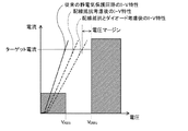
図16は、図1に示す半導体集積回路装置に図15に示す静電気保護回路を適用した場合のI−V特性を示す図である。図16において、横軸は、放電経路における静電気保護回路等の両端間の電圧を表しており、縦軸は、放電経路に流れる電流を表している。 16 is a diagram showing IV characteristics when the electrostatic protection circuit shown in FIG. 15 is applied to the semiconductor integrated circuit device shown in FIG. In FIG. 16, the horizontal axis represents the voltage between both ends of the electrostatic protection circuit or the like in the discharge path, and the vertical axis represents the current flowing in the discharge path.
図16に示すように、本発明の第6の実施形態に係る静電気保護回路10eは、両端間の電圧が絶対最大定格電圧VABS以下の領域においては保護動作を開始しないので、放電経路に電流が流れない。一方、端子間の電圧が所定の電圧VP1を超えると、静電気保護回路10eが保護動作を開始して、放電経路に電流が流れ始める。
As shown in FIG. 16, the
放電経路に流れる電流が第1の所定の電流IP1〜第2の所定の電流IP2である第1の動作領域においては、放電経路に流れる電流が大きくなるほど、静電気保護回路10eの両端間の電圧が低下する。放電経路に流れる電流が第2の所定の電流IP2を超える第2の動作領域においては、静電気保護回路10eが両端間の電圧を略一定に保つ。
In the first operation region in which the current flowing through the discharge path is the first predetermined current I P1 to the second predetermined current I P2 , the larger the current flowing through the discharge path, the greater the distance between both ends of the
これにより、配線抵抗やダイオードに発生する電圧を考慮しても、放電経路に流れる電流がターゲット電流に達したときに、半導体集積回路装置の端子間の電圧と内部回路20の素子が破壊に至る電圧VDMGとの間には、第4の実施形態におけるよりも大きい電圧マージンが存在する。
Thus, even when the wiring resistance and the voltage generated in the diode are taken into account, when the current flowing through the discharge path reaches the target current, the voltage between the terminals of the semiconductor integrated circuit device and the element of the
<第7の実施形態>
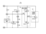
図17は、本発明の第7の実施形態に係る静電気保護回路の構成例を示す回路図である。第7の実施形態に係る静電気保護回路10fは、図6に示す第4の実施形態に係る静電気保護回路10cにおいて、ノードN4とノードN5との間に複数の抵抗素子が直列に接続され、それらの抵抗素子の内の少なくとも1つと並列に接続された少なくとも1つのNチャネルトランジスターが追加されており、キャパシターC1をさらに含んでも良い。その他の点に関し、図17に示す静電気保護回路10fは、図6に示す静電気保護回路10cと同様である。
<Seventh Embodiment>
FIG. 17 is a circuit diagram showing a configuration example of an electrostatic protection circuit according to the seventh embodiment of the present invention. The
図17においては、一例として、ノードN4とノードN5との間に直列に接続された抵抗素子R3〜R5と、抵抗素子R3及びR4にそれぞれ並列に接続されたNチャネルMOSトランジスターQN14及びQN15とが示されている。このように、分圧回路を構成する複数の抵抗素子にそれぞれ並列に接続された複数のトランジスターを設けても良い。 In FIG. 17, as an example, resistance elements R3 to R5 connected in series between node N4 and node N5, and N channel MOS transistors QN14 and QN15 connected in parallel to resistance elements R3 and R4, respectively. It is shown. As described above, a plurality of transistors connected in parallel to the plurality of resistance elements constituting the voltage dividing circuit may be provided.
トランジスターQN14は、抵抗素子R3の一端に接続されたドレインと、抵抗素子R3の他端に接続されたソースと、検出回路13の出力端子OUTに接続されたゲートとを有し、検出回路13の出力信号がハイレベルに活性化されたときにオンする。また、トランジスターQN15は、抵抗素子R4の一端に接続されたドレインと、抵抗素子R4の他端に接続されたソースと、検出回路13の出力端子OUTに接続されたゲートとを有し、検出回路13の出力信号がハイレベルに活性化されたときにオンする。
The transistor QN14 has a drain connected to one end of the resistance element R3, a source connected to the other end of the resistance element R3, and a gate connected to the output terminal OUT of the
トランジスターQN14及びQN15は、抵抗素子R2〜R5と共に、分圧回路を構成している。静電気の放電により、検出回路13の出力信号がハイレベルに活性化されて、静電気保護回路10fが保護動作を一旦開始すると、トランジスターQN14及びQN15がオンして、分圧回路における分圧比が上昇する。その結果、ノードN1とノードN2との間の電圧が低下し、半導体集積回路装置の内部回路が破壊に至る電圧に対するマージンが増えて静電気耐量が向上する。従って、第7の実施形態に係る静電気保護回路10fも、第6の実施形態に係る静電気保護回路10eのI−V特性と同様のI−V特性を有するが、第6の実施形態におけるよりもI−V特性をきめ細やかに自由に設定することができる。
Transistors QN14 and QN15 together with resistance elements R2 to R5 form a voltage dividing circuit. Due to the discharge of static electricity, the output signal of the
<第8の実施形態>
図18は、本発明の第8の実施形態に係る静電気保護回路の構成例を示す回路図である。本発明の第1〜第7の実施形態において、第1のインピーダンス素子として、抵抗素子R1(図3等)の替りにPチャネルMOSトランジスターを用いても良い。また、第2のインピーダンス素子として、抵抗素子R2(図3等)の替りにNチャネルMOSトランジスターを用いても良い。
<Eighth Embodiment>
FIG. 18 is a circuit diagram showing a configuration example of an electrostatic protection circuit according to the eighth embodiment of the present invention. In the first to seventh embodiments of the present invention, a P-channel MOS transistor may be used as the first impedance element instead of the resistance element R1 (FIG. 3 and the like). Further, as the second impedance element, an N-channel MOS transistor may be used instead of the resistance element R2 (FIG. 3 and the like).
図18においては、一例として、図3に示す第1の実施形態に係る静電気保護回路10において、第1のインピーダンス素子としてPチャネルMOSトランジスターQP30を用いると共に、第2のインピーダンス素子としてNチャネルMOSトランジスターQN30を用いた静電気保護回路10gが示されている。その他の点に関し、図18に示す静電気保護回路10gは、図3に示す静電気保護回路10と同様である。
18, as an example, in the
トランジスターQP30は、ノードN1に接続されたソースと、ノードN3に接続されたドレインと、ノードN2に接続されたゲートとを有している。ノードN1とノードN2との間にトランジスターQP30の閾値電圧よりも大きい正の電圧が印加されると、トランジスターQP30がオンする。 Transistor QP30 has a source connected to node N1, a drain connected to node N3, and a gate connected to node N2. When a positive voltage larger than the threshold voltage of the transistor QP30 is applied between the node N1 and the node N2, the transistor QP30 is turned on.
トランジスターQP30のオン抵抗は、ノードN1とノードN2との間の電圧に依存する。放電回路12がノードN1からノードN2に電流を流すと、ノードN1とノードN2との間の電圧が減少するが、トランジスターQP30のオン抵抗が増加するので、ノードN1とノードN3との間の電圧の減少が抑えられる。従って、保護動作の途中でトランジスターQP10がオフすることを防止できる。
The on-resistance of the transistor QP30 depends on the voltage between the node N1 and the node N2. When the
また、製造工程におけるPチャネルMOSトランジスターのばらつきに対して、トランジスターQP10の特性変動とトランジスターQP30の特性変動とが相殺するので、全体として特性変動が小さい静電気保護回路を提供することができる。さらに、抵抗素子をPチャネルMOSトランジスターに置き換えることにより、半導体集積回路装置のコストを低減することができる。 In addition, since the characteristic variation of the transistor QP10 and the characteristic variation of the transistor QP30 cancel each other with respect to the variation of the P-channel MOS transistor in the manufacturing process, an electrostatic protection circuit with small characteristic variation as a whole can be provided. Furthermore, the cost of the semiconductor integrated circuit device can be reduced by replacing the resistance element with a P-channel MOS transistor.
トランジスターQN30は、ノードN4に接続されたドレインと、ノードN2に接続されたソースと、ノードN1に接続されたゲートとを有している。ノードN1とノードN2との間にトランジスターQN30の閾値電圧よりも大きい正の電圧が印加されると、トランジスターQN30がオンする。 Transistor QN30 has a drain connected to node N4, a source connected to node N2, and a gate connected to node N1. When a positive voltage larger than the threshold voltage of the transistor QN30 is applied between the node N1 and the node N2, the transistor QN30 is turned on.
トランジスターQN30のオン抵抗は、ノードN1とノードN2との間の電圧に依存する。放電回路12がノードN1からノードN2に電流を流すと、ノードN1とノードN2との間の電圧が減少するが、トランジスターQN30のオン抵抗が増加するので、ノードN4とノードN2との間の電圧の減少が抑えられる。従って、保護動作の途中でトランジスターQN10がオフすることを防止できる。
The on-resistance of the transistor QN30 depends on the voltage between the node N1 and the node N2. When the
また、製造工程におけるNチャネルMOSトランジスターのばらつきに対して、トランジスターQN10の特性変動とトランジスターQN30の特性変動とが相殺するので、全体として特性変動が小さい静電気保護回路を提供することができる。さらに、抵抗素子をNチャネルMOSトランジスターに置き換えることにより、半導体集積回路装置のコストを低減することができる。 In addition, since the characteristic variation of the transistor QN10 and the characteristic variation of the transistor QN30 cancel each other with respect to variations in the N-channel MOS transistor in the manufacturing process, an electrostatic protection circuit with small characteristic variation as a whole can be provided. Furthermore, the cost of the semiconductor integrated circuit device can be reduced by replacing the resistance element with an N-channel MOS transistor.
<第9の実施形態>
図19は、本発明の第9の実施形態に係る静電気保護回路の構成例を示す回路図である。本発明の第1〜第7の実施形態において、第1のトランジスターとしてNチャネルMOSトランジスターを用い、第2のトランジスターとしてPチャネルMOSトランジスターを用いて、それに応じて各素子の接続を変更しても良い。
<Ninth Embodiment>
FIG. 19 is a circuit diagram showing a configuration example of an electrostatic protection circuit according to the ninth embodiment of the present invention. In the first to seventh embodiments of the present invention, an N-channel MOS transistor is used as the first transistor and a P-channel MOS transistor is used as the second transistor, and the connection of each element is changed accordingly. good.
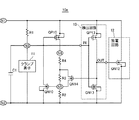
図19においては、一例として、図15に示す第6の実施形態に係る静電気保護回路10eにおいて、第1のトランジスターとしてNチャネルMOSトランジスターQN10を用い、第2のトランジスターとしてPチャネルMOSトランジスターQP10を用い、第3のトランジスターとしてPチャネルMOSトランジスターQP14を用いた静電気保護回路10hが示されている。
In FIG. 19, as an example, in the
静電気保護回路10hは、クランプ素子11と、抵抗素子R1〜R3と、NチャネルMOSトランジスターQN10と、PチャネルMOSトランジスターQP10及びQP14と、検出回路13と、放電回路12hとを含んでいる。また、静電気保護回路10hは、抵抗素子R4、及び/又は、クランプ素子11と並列に接続されたキャパシターをさらに含んでも良い。
The
ノードN3において互いに接続されたクランプ素子11及び抵抗素子R1を含む直列回路が、ノードN1とノードN2との間に接続されている。本実施形態においては、クランプ素子11が、ノードN1とノードN3との間に接続されており、抵抗素子R1が、ノードN3とノードN2との間に接続されている。
A series circuit including the
トランジスターQN10は、ノードN4とノードN2との間に接続され、抵抗素子R1に発生する電圧の上昇に従ってオンする。即ち、トランジスターQN10は、ノードN4に接続されたドレインと、ノードN2に接続されたソースと、ノードN3に接続されたゲートとを有しており、ノードN3とノードN2との間の電圧が閾値電圧を超えるとオンする。 The transistor QN10 is connected between the node N4 and the node N2, and is turned on as the voltage generated in the resistance element R1 increases. That is, the transistor QN10 has a drain connected to the node N4, a source connected to the node N2, and a gate connected to the node N3, and the voltage between the node N3 and the node N2 is a threshold value. Turns on when the voltage is exceeded.
抵抗素子R3及びR4は、ノードN4とノードN5との間に直列に接続されており、抵抗素子R2は、ノードN5とノードN1との間に接続されている。また、トランジスターQP14は、抵抗素子R3と並列に接続されている。即ち、トランジスターQP14は、抵抗素子R3の一端に接続されたソースと、抵抗素子R3の他端に接続されたドレインと、検出回路13の出力端子OUTに接続されたゲートとを有している。抵抗素子R2〜R4及びトランジスターQP14は、ノードN1とノードN4との間の電圧を分圧する分圧回路を構成している。
The resistance elements R3 and R4 are connected in series between the node N4 and the node N5, and the resistance element R2 is connected between the node N5 and the node N1. The transistor QP14 is connected in parallel with the resistance element R3. That is, the transistor QP14 has a source connected to one end of the resistance element R3, a drain connected to the other end of the resistance element R3, and a gate connected to the output terminal OUT of the
トランジスターQP10は、分圧回路によって分圧された電圧の上昇に従ってオンし、抵抗素子R1に流れる電流を増加させる。即ち、トランジスターQP10は、ノードN1に接続されたソースと、ノードN3に接続されたドレインと、ノードN5に接続されたゲートとを有しており、ノードN1とノードN5との間の電圧が閾値電圧を超えるとオンする。 The transistor QP10 turns on as the voltage divided by the voltage dividing circuit increases, and increases the current flowing through the resistance element R1. That is, the transistor QP10 has a source connected to the node N1, a drain connected to the node N3, and a gate connected to the node N5, and the voltage between the node N1 and the node N5 is a threshold value. Turns on when the voltage is exceeded.
検出回路13は、トランジスターQP10がオン状態であることを検出したときに出力信号を活性化する。例えば、検出回路13は、PチャネルMOSトランジスターQP13とNチャネルMOSトランジスターQN13とによって構成されるインバーターを含んでいる。その場合に、検出回路13は、抵抗素子R1に発生する電圧がノードN1とノードN2との間の電圧に対して所定の割合(例えば、50%)よりも大きくなったときに出力信号をローレベルに活性化する。
The
放電回路12hは、例えば、PチャネルMOSトランジスターQP12を含んでいる。トランジスターQP12は、ノードN1に接続されたソースと、ノードN2に接続されたドレインと、検出回路13の出力信号が供給されるゲートとを有している。放電回路12hは、検出回路13の出力信号がローレベルに活性化されたときに、ノードN1からノードN2に電流を流す。
The
ここで、図19に示す静電気保護回路10hの動作について説明する。
通常動作時において、ノードN1とノードN2との間に印加される正の電圧(ノードN1の電位>ノードN2の電位)がクランプ電圧よりも小さい場合には、クランプ素子11及び抵抗素子R1に殆ど電流が流れないので、ノードN3とノードN2との間の電圧がトランジスターQN10の閾値電圧よりも小さいままとなり、トランジスターQN10がオフ状態を維持する。
Here, the operation of the
In a normal operation, when the positive voltage applied between the node N1 and the node N2 (the potential of the node N1> the potential of the node N2) is smaller than the clamp voltage, the
一方、静電気の放電によって、ノードN1とノードN2との間にクランプ電圧以上の電圧が印加されると、ノードN1からクランプ素子11及び抵抗素子R1を介してノードN2に電流が流れる。ノードN1とノードN2との間の電圧がさらに上昇して、ノードN3とノードN2との間の電圧がトランジスターQN10の閾値電圧以上になると、トランジスターQN10がオンする。ただし、この時点においては、検出回路13の入力端子INの電位はローレベルとなっている。
On the other hand, when a voltage equal to or higher than the clamp voltage is applied between the node N1 and the node N2 due to electrostatic discharge, a current flows from the node N1 to the node N2 via the
トランジスターQN10がオンすることにより、抵抗素子R2〜R4等によって構成される分圧回路に電圧が印加されて、ノードN1とノードN5との間の電圧が0Vから上昇する。ここで、ノードN1とノードN2との間の電圧が所定の値以上であれば、ノードN1とノードN5との間の電圧がトランジスターQP10の閾値電圧以上になって、トランジスターQP10がオンする。 When transistor QN10 is turned on, a voltage is applied to the voltage dividing circuit constituted by resistance elements R2 to R4 and the like, and the voltage between nodes N1 and N5 rises from 0V. If the voltage between the node N1 and the node N2 is equal to or higher than a predetermined value, the voltage between the node N1 and the node N5 becomes equal to or higher than the threshold voltage of the transistor QP10, and the transistor QP10 is turned on.
トランジスターQP10がオンすることにより、抵抗素子R1に流れる電流が増加して、ノードN3とノードN2との間の電圧が上昇するので、トランジスターQN10に流れる電流が増加する(正帰還)。同時に、検出回路13の入力端子INの電位がハイレベルとなり、検出回路13の出力信号がローレベルに活性化される。これにより、放電回路12hのトランジスターQP12が、ノードN1からノードN2に電流を流し始める。
When the transistor QP10 is turned on, the current flowing through the resistance element R1 increases and the voltage between the node N3 and the node N2 increases, so that the current flowing through the transistor QN10 increases (positive feedback). At the same time, the potential of the input terminal IN of the
検出回路13の出力信号がローレベルに活性化されて、静電気保護回路10hが保護動作を一旦開始すると、トランジスターQP14がオンして、分圧回路における分圧比が上昇する。その結果、ノードN1とノードN2との間の電圧が低下し、半導体集積回路装置の内部回路が破壊に至る電圧に対するマージンが増えて静電気耐量が向上する。
When the output signal of the
放電回路12hのトランジスターQP12に流れる電流によって、ノードN1とノードN2との間の電圧がさらに低下すると、ノードN1とノードN5との間の電圧がトランジスターQP10の閾値電圧よりも低下するので、トランジスターQP10がオン状態からオフ状態に遷移する。その結果、抵抗素子R1に流れる電流が減少するので、検出回路13の出力信号がハイレベルに非活性化され、放電回路12hのトランジスターQP12がオン状態からオフ状態に遷移して、ノードN1とノードN2との間の電圧が略一定に保持される。
When the voltage between the node N1 and the node N2 is further reduced by the current flowing through the transistor QP12 of the
本実施形態において、第1のインピーダンス素子として、抵抗素子R1の替りにNチャネルMOSトランジスターを用いても良い。その場合に、NチャネルMOSトランジスターは、ノードN3に接続されたドレインと、ノードN2に接続されたソースと、ノードN1に接続されたゲートを有する。 In the present embodiment, an N-channel MOS transistor may be used as the first impedance element instead of the resistance element R1. In that case, the N-channel MOS transistor has a drain connected to node N3, a source connected to node N2, and a gate connected to node N1.
このNチャネルMOSトランジスターのオン抵抗は、ノードN1とノードN2との間の電圧に依存する。放電回路12hがノードN1からノードN2に電流を流すと、ノードN1とノードN2との間の電圧が減少するが、NチャネルMOSトランジスターのオン抵抗が増加するので、ノードN3とノードN2との間の電圧の減少が抑えられる。従って、保護動作の途中でトランジスターQN10がオフすることを防止できる。
The on-resistance of the N channel MOS transistor depends on the voltage between the node N1 and the node N2. When the
また、第2のインピーダンス素子として、抵抗素子R2の替りにPチャネルMOSトランジスターを用いても良い。その場合に、PチャネルMOSトランジスターは、ノードN1に接続されたソースと、ノードN5に接続されたドレインと、ノードN2に接続されたゲートとを有する。 Further, as the second impedance element, a P-channel MOS transistor may be used instead of the resistance element R2. In that case, the P-channel MOS transistor has a source connected to node N1, a drain connected to node N5, and a gate connected to node N2.
このPチャネルMOSトランジスターのオン抵抗は、ノードN1とノードN2との間の電圧に依存する。放電回路12hがノードN1からノードN2に電流を流すと、ノードN1とノードN2との間の電圧が減少するが、PチャネルMOSトランジスターのオン抵抗が増加するので、ノードN1とノードN5との間の電圧の減少が抑えられる。従って、保護動作の途中でトランジスターQP10がオフすることを防止できる。
The on-resistance of the P channel MOS transistor depends on the voltage between the node N1 and the node N2. When
<第10の実施形態>
図20は、本発明の第10の実施形態に係る静電気保護回路の構成例を示す回路図である。第10の実施形態に係る静電気保護回路10iにおいては、図19に示す第9の実施形態における検出回路13の替りに検出回路13iが用いられ、放電回路12hの替りに放電回路12が用いられる。その他の点に関し、図20に示す静電気保護回路10iは、図19に示す静電気保護回路10hと同様である。
<Tenth Embodiment>
FIG. 20 is a circuit diagram showing a configuration example of the electrostatic protection circuit according to the tenth embodiment of the present invention. In the
検出回路13iは、トランジスターQP10がオン状態であることを検出したときに出力信号を活性化する。例えば、検出回路13iは、直列に接続された第1のインバーター及び第2のインバーターを含んでいる。第1のインバーターは、PチャネルMOSトランジスターQP41とNチャネルMOSトランジスターQN41とによって構成される、また、第2のインバーターは、PチャネルMOSトランジスターQP42とNチャネルMOSトランジスターQN42とによって構成される。 The detection circuit 13i activates the output signal when detecting that the transistor QP10 is in the ON state. For example, the detection circuit 13i includes a first inverter and a second inverter connected in series. The first inverter is composed of a P-channel MOS transistor QP41 and an N-channel MOS transistor QN41, and the second inverter is composed of a P-channel MOS transistor QP42 and an N-channel MOS transistor QN42.
第1のインバーターは、入力端子INに供給されるノードN3の電位がハイレベルであるかローレベルであるかを検出し、そのレベルを反転して、反転されたレベルを有する第1の出力信号を出力端子OUT1から出力する。また、第2のインバーターは、第1の出力信号がハイレベルであるかローレベルであるかを検出し、そのレベルを反転して、反転されたレベルを有する第2の出力信号を出力端子OUT2から出力する。 The first inverter detects whether the potential of the node N3 supplied to the input terminal IN is high level or low level, inverts the level, and outputs the first output signal having the inverted level Is output from the output terminal OUT1. The second inverter detects whether the first output signal is at a high level or a low level, inverts the level, and outputs the second output signal having the inverted level to the output terminal OUT2. Output from.
これにより、検出回路13iは、抵抗素子R1に発生する電圧がノードN1とノードN2との間の電圧に対して所定の割合(例えば、50%)よりも大きくなったときに、第1の出力信号をローレベルに活性化すると共に、第2の出力信号をハイレベルに活性化する。検出回路13iの第1の出力信号は、分圧回路のトランジスターQP14のゲートに供給される。また、検出回路13iの第2の出力信号は、放電回路12のトランジスターQN12のゲートに供給される。
Thereby, the detection circuit 13i outputs the first output when the voltage generated in the resistance element R1 becomes larger than a predetermined ratio (for example, 50%) with respect to the voltage between the nodes N1 and N2. The signal is activated to a low level, and the second output signal is activated to a high level. The first output signal of the detection circuit 13i is supplied to the gate of the transistor QP14 of the voltage dividing circuit. The second output signal of the detection circuit 13i is supplied to the gate of the transistor QN12 of the
本実施形態によれば、放電回路12において、NチャネルMOSトランジスター又はNPNバイポーラトランジスターを用いることができる。NチャネルMOSトランジスター又はNPNバイポーラトランジスターは、P型半導体基板にウエルを介さずに形成することが可能であり、特性的にも優れている。
According to the present embodiment, an N-channel MOS transistor or an NPN bipolar transistor can be used in the
<インピーダンス素子の例>
図21は、本発明の各実施形態において抵抗素子以外に使用可能なインピーダンス素子の例を示す図である。本発明の各実施形態においては、抵抗素子R3〜R5のいずれかの替りに、図21の(a)〜(h)に示すインピーダンス素子を用いることができる。なお、図21において、「N+」は、高電位側のノードを表しており、「N−」は、低電位側のノードを表している。
<Example of impedance element>
FIG. 21 is a diagram illustrating examples of impedance elements that can be used in addition to the resistance elements in the embodiments of the present invention. In each embodiment of the present invention, impedance elements shown in FIGS. 21A to 21H can be used instead of any of the resistance elements R3 to R5. In FIG. 21, “N +” represents a node on the high potential side, and “N−” represents a node on the low potential side.
図21(a)は、高電位側のノードN+に接続されたカソードと、低電位側のノードN−に接続されたアノードとを有するダイオードD1を示している。このダイオードD1を、例えば、図6に示す第4の実施形態に係る静電気保護回路10cにおいて、抵抗素子R3の替りに用いることができる。
FIG. 21A shows a diode D1 having a cathode connected to the node N + on the high potential side and an anode connected to the node N− on the low potential side. This diode D1 can be used in place of the resistance element R3 in the
図6において、ノードN1とノードN2との間に高電圧が印加されて、ノードN1とノードN3との間の電圧が上昇してトランジスターQP10の閾値電圧以上になると、トランジスターQP10がオンする。トランジスターQP10から印加される電圧によってダイオードD1がブレークダウンすると、抵抗素子R2に電流が流れて、ノードN5とノードN2との間の電圧が0Vから上昇する。 In FIG. 6, when a high voltage is applied between the node N1 and the node N2 and the voltage between the node N1 and the node N3 increases and becomes equal to or higher than the threshold voltage of the transistor QP10, the transistor QP10 is turned on. When the diode D1 breaks down due to the voltage applied from the transistor QP10, a current flows through the resistance element R2, and the voltage between the node N5 and the node N2 rises from 0V.
抵抗素子R3の替りにダイオードD1を用いる場合の静電気保護回路10cの保持電圧VHは、次式(7)によって近似される。
VH≒VthQN10+VBD1 ・・・(7)
ここで、VthQN10はトランジスターQN10の閾値電圧であり、VBD1はダイオードD1のブレークダウン電圧である。
Holding voltage V H of the
V H ≈Vth QN10 + V BD1 (7)
Here, Vth QN10 is the threshold voltage of the transistor QN10, V BD1 is the breakdown voltage of the diode D1.
式(3)においては、保持電圧VHが、トランジスターQN10の閾値電圧VthQN10のばらつきに対して(R2+R3)/R2倍のばらつきを有する。これに対し、ダイオードD1のブレークダウン電圧VBD1のばらつきはトランジスターQN10の閾値電圧VthQN10のばらつきと比較して小さいので、式(7)における保持電圧VHのばらつきは、トランジスターQN10の閾値電圧VthQN10のばらつきに略依存する。従って、トランジスターQN10の閾値電圧VthQN10のばらつきに対して保持電圧VHの変動が少ない静電気保護回路を提供することができる。 In Expression (3), the holding voltage V H has a variation of (R 2 + R 3 ) / R 2 times the variation of the threshold voltage Vth QN10 of the transistor QN10. Since contrast, variation in the breakdown voltage V BD1 of the diode D1 is small compared to the variation in the threshold voltage Vth QN10 transistors QN10, variations in the holding voltage V H in the formula (7), the threshold voltage Vth of the transistor QN10 It depends substantially on the variation of QN10 . Therefore, it is possible to provide an electrostatic protection circuit with less fluctuation of the holding voltage V H for variations in the threshold voltage Vth QN10 transistors QN10.
図21(b)は、高電位側のノードN+に接続されたアノードと、低電位側のノードN−に接続されたカソードとを有するダイオードD2を示している。このダイオードD2を、例えば、図6に示す第4の実施形態に係る静電気保護回路10cにおいて、抵抗素子R3の替りに用いることができる。
FIG. 21B shows a diode D2 having an anode connected to the node N + on the high potential side and a cathode connected to the node N− on the low potential side. This diode D2 can be used in place of the resistance element R3 in the
図6において、ノードN1とノードN2との間に高電圧が印加されて、ノードN1とノードN3との間の電圧が上昇してトランジスターQP10の閾値電圧以上になると、トランジスターQP10がオンする。トランジスターQP10から印加される電圧によってダイオードD2に順方向電流が流れると、抵抗素子R2にも電流が流れて、ノードN5とノードN2との間の電圧が0Vから上昇する。 In FIG. 6, when a high voltage is applied between the node N1 and the node N2 and the voltage between the node N1 and the node N3 increases and becomes equal to or higher than the threshold voltage of the transistor QP10, the transistor QP10 is turned on. When a forward current flows through the diode D2 due to the voltage applied from the transistor QP10, a current also flows through the resistance element R2, and the voltage between the node N5 and the node N2 rises from 0V.
抵抗素子R3の替りにダイオードD2を用いる場合の静電気保護回路10cの保持電圧VHは、次式(8)によって近似される。
VH≒VthQN10+VFD2 ・・・(8)
ここで、VthQN10はトランジスターQN10の閾値電圧であり、VFD2はダイオードD2の順方向電圧である。
Holding voltage V H of the
V H ≈Vth QN10 + V FD2 (8)
Here, Vth QN10 is the threshold voltage of the transistor QN10, V FD2 is the forward voltage of the diode D2.
式(3)においては、保持電圧VHが、トランジスターQN10の閾値電圧VthQN10のばらつきに対して(R2+R3)/R2倍のばらつきを有する。これに対し、式(8)における保持電圧VHのばらつきは、トランジスターQN10の閾値電圧VthQN10のばらつきとダイオードD2の順方向電圧VFD2のばらつきとの和であり、ダイオードD2の順方向電圧VFD2の量産ばらつきは小さい。従って、トランジスターQN10の閾値電圧VthQN10のばらつきに対して保持電圧VHの変動が少ない静電気保護回路を提供することができる。また、ダイオードD2の順方向電圧VFD2は比較的小さいので、保持電圧VHを低く設定することができる。 In Expression (3), the holding voltage V H has a variation of (R 2 + R 3 ) / R 2 times the variation of the threshold voltage Vth QN10 of the transistor QN10. On the other hand, the variation in the holding voltage V H in the equation (8) is the sum of the variation in the threshold voltage Vth QN10 of the transistor QN10 and the variation in the forward voltage V FD2 of the diode D2, and the forward voltage V of the diode D2. Variation in mass production of FD2 is small. Therefore, it is possible to provide an electrostatic protection circuit with less fluctuation of the holding voltage V H for variations in the threshold voltage Vth QN10 transistors QN10. Further, since the forward voltage V FD2 of the diode D2 is relatively small, the holding voltage V H can be set low.
図21(c)は、高電位側のノードN+に接続されたソースと、低電位側のノードN−に接続されたドレイン及びゲートとを有するPチャネルMOSトランジスターQP1を示している。このトランジスターQP1を、例えば、図6に示す第4の実施形態に係る静電気保護回路10cにおいて、抵抗素子R3の替りに用いることができる。
FIG. 21C shows a P-channel MOS transistor QP1 having a source connected to the node N + on the high potential side, and a drain and a gate connected to the node N− on the low potential side. This transistor QP1 can be used, for example, in place of the resistance element R3 in the
図6において、ノードN1とノードN2との間に高電圧が印加されて、ノードN1とノードN3との間の電圧が上昇してトランジスターQP10の閾値電圧以上になると、トランジスターQP10がオンする。トランジスターQP10から印加される電圧によってトランジスターQP1に電流が流れると、抵抗素子R2にも電流が流れて、ノードN5とノードN2との間の電圧が0Vから上昇する。ここで、トランジスターQP1のゲートはドレインに接続されているので、トランジスターQP1は飽和領域で動作する。従って、ドレイン電流が十分小さい範囲において、トランジスターQP1のソース・ドレイン間電圧は、閾値電圧VthQP1に略等しくなる。 In FIG. 6, when a high voltage is applied between the node N1 and the node N2 and the voltage between the node N1 and the node N3 increases and becomes equal to or higher than the threshold voltage of the transistor QP10, the transistor QP10 is turned on. When a current flows through the transistor QP1 due to the voltage applied from the transistor QP10, a current also flows through the resistance element R2, and the voltage between the node N5 and the node N2 rises from 0V. Here, since the gate of the transistor QP1 is connected to the drain, the transistor QP1 operates in the saturation region. Therefore, in the range where the drain current is sufficiently small, the source-drain voltage of the transistor QP1 is substantially equal to the threshold voltage Vth QP1 .
抵抗素子R3の替りにトランジスターQP1を用いる場合の静電気保護回路10cの保持電圧VHは、次式(9)によって近似される。
VH≒VthQN10+VthQP1 ・・・(9)
ここで、VthQN10はトランジスターQN10の閾値電圧であり、VthQP1はトランジスターQP1の閾値電圧である。
Holding voltage V H of the
V H ≈Vth QN10 + Vth QP1 (9)
Here, Vth QN10 is a threshold voltage of the transistor QN10, and Vth QP1 is a threshold voltage of the transistor QP1.
式(3)においては、保持電圧VHが、トランジスターQN10の閾値電圧VthQN10のばらつきに対して(R2+R3)/R2倍のばらつきを有する。これに対し、式(9)における保持電圧VHのばらつきは、トランジスターQN10の閾値電圧VthQN10のばらつきとトランジスターQP1の閾値電圧VthQP1のばらつきとの和となる。従って、トランジスターQN10の閾値電圧VthQN10のばらつきに対して保持電圧VHの変動が少ない静電気保護回路を提供することができる。また、トランジスターQP1の閾値電圧VthQP1は比較的小さいので、保持電圧VHを低く設定することができる。 In Expression (3), the holding voltage V H has a variation of (R 2 + R 3 ) / R 2 times the variation of the threshold voltage Vth QN10 of the transistor QN10. In contrast, variations in the holding voltage V H in Equation (9) is the sum of the variation in the threshold voltage Vth QP1 variation and transistor QP1 threshold voltage Vth QN10 transistors QN10. Therefore, it is possible to provide an electrostatic protection circuit with less fluctuation of the holding voltage V H for variations in the threshold voltage Vth QN10 transistors QN10. Further, since the threshold voltage Vth QP1 of the transistor QP1 is relatively small, it is possible to set a low holding voltage V H.
図21(d)は、高電位側のノードN+に接続されたソース及びゲートと、低電位側のノードN−に接続されたドレインとを有するPチャネルMOSトランジスターQP2を示している。このトランジスターQP2を、例えば、図6に示す第4の実施形態に係る静電気保護回路10cにおいて、抵抗素子R3の替りに用いることができる。
FIG. 21D shows a P-channel MOS transistor QP2 having a source and a gate connected to the node N + on the high potential side, and a drain connected to the node N− on the low potential side. This transistor QP2 can be used in place of the resistance element R3 in the
図6において、ノードN1とノードN2との間に高電圧が印加されて、ノードN1とノードN3との間の電圧が上昇してトランジスターQP10の閾値電圧以上になると、トランジスターQP10がオンする。トランジスターQP10から印加される電圧によってトランジスターQP2がブレークダウンすると、抵抗素子R2に電流が流れて、ノードN5とノードN2との間の電圧が0Vから上昇する。 In FIG. 6, when a high voltage is applied between the node N1 and the node N2 and the voltage between the node N1 and the node N3 increases and becomes equal to or higher than the threshold voltage of the transistor QP10, the transistor QP10 is turned on. When the transistor QP2 breaks down due to the voltage applied from the transistor QP10, a current flows through the resistance element R2, and the voltage between the node N5 and the node N2 rises from 0V.
抵抗素子R3の替りにトランジスターQP2を用いる場合の静電気保護回路10cの保持電圧VHは、次式(10)によって近似される。
VH≒VthQN10+VBQP2 ・・・(10)
ここで、VthQN10はトランジスターQN10の閾値電圧であり、VBQP2はトランジスターQP2のブレークダウン電圧である。
Holding voltage V H of the
V H ≈Vth QN10 + V BQP2 (10)
Here, Vth QN10 is a threshold voltage of the transistor QN10, and VBQP2 is a breakdown voltage of the transistor QP2.
式(3)においては、保持電圧VHが、トランジスターQN10の閾値電圧VthQN10のばらつきに対して(R2+R3)/R2倍のばらつきを有する。これに対し、式(10)における保持電圧VHのばらつきは、トランジスターQN10の閾値電圧VthQN10のばらつきとトランジスターQP2のブレークダウン電圧VBQP2のばらつきとの和となる。従って、トランジスターQN10の閾値電圧VthQN10のばらつきに対して保持電圧VHの変動が少ない静電気保護回路を提供することができる。 In Expression (3), the holding voltage V H has a variation of (R 2 + R 3 ) / R 2 times the variation of the threshold voltage Vth QN10 of the transistor QN10. In contrast, variations in the holding voltage V H in the formula (10) is the sum of the variation in the breakdown voltage V BQP2 variation and transistor QP2 threshold voltage Vth QN10 transistors QN10. Therefore, it is possible to provide an electrostatic protection circuit with less fluctuation of the holding voltage V H for variations in the threshold voltage Vth QN10 transistors QN10.
図21(e)は、高電位側のノードN+に接続されたドレイン及びゲートと、低電位側のノードN−に接続されたソースとを有するNチャネルMOSトランジスターQN1を示している。このトランジスターQN1を、例えば、図6に示す第4の実施形態に係る静電気保護回路10cにおいて、抵抗素子R3の替りに用いることができる。
FIG. 21E shows an N-channel MOS transistor QN1 having a drain and a gate connected to the node N + on the high potential side and a source connected to the node N− on the low potential side. This transistor QN1 can be used, for example, in place of the resistance element R3 in the
図6において、ノードN1とノードN2との間に高電圧が印加されて、ノードN1とノードN3との間の電圧が上昇してトランジスターQP10の閾値電圧以上になると、トランジスターQP10がオンする。トランジスターQP10から印加される電圧によってトランジスターQN1に電流が流れると、抵抗素子R2にも電流が流れて、ノードN5とノードN2との間の電圧が0Vから上昇する。ここで、トランジスターQN1のゲートはドレインに接続されているので、トランジスターQN1は飽和領域で動作する。従って、ドレイン電流が十分小さい範囲において、トランジスターQN1のドレイン・ソース間電圧は、閾値電圧VthQN1に略等しくなる。 In FIG. 6, when a high voltage is applied between the node N1 and the node N2 and the voltage between the node N1 and the node N3 increases and becomes equal to or higher than the threshold voltage of the transistor QP10, the transistor QP10 is turned on. When a current flows through the transistor QN1 due to the voltage applied from the transistor QP10, a current also flows through the resistance element R2, and the voltage between the node N5 and the node N2 rises from 0V. Here, since the gate of the transistor QN1 is connected to the drain, the transistor QN1 operates in the saturation region. Therefore, the drain-source voltage of the transistor QN1 is substantially equal to the threshold voltage Vth QN1 in a range where the drain current is sufficiently small.
抵抗素子R3の替りにトランジスターQN1を用いる場合の静電気保護回路10cの保持電圧VHは、次式(11)によって近似される。
VH≒VthQN10+VthQN1 ・・・(11)
ここで、VthQN10はトランジスターQN10の閾値電圧であり、VthQN1はトランジスターQN1の閾値電圧である。
Holding voltage V H of the
V H ≈Vth QN10 + Vth QN1 (11)
Here, Vth QN10 is a threshold voltage of the transistor QN10, and Vth QN1 is a threshold voltage of the transistor QN1.
式(3)においては、保持電圧VHが、トランジスターQN10の閾値電圧VthQN10のばらつきに対して(R2+R3)/R2倍のばらつきを有する。これに対し、式(11)における保持電圧VHのばらつきは、トランジスターQN10の閾値電圧VthQN10のばらつきとトランジスターQN1の閾値電圧VthQN1のばらつきとの和となる。従って、トランジスターQN10の閾値電圧VthQN10のばらつきに対して保持電圧VHの変動が少ない静電気保護回路を提供することができる。また、トランジスターQN1の閾値電圧VthQN1は比較的小さいので、保持電圧VHを低く設定することができる。 In Expression (3), the holding voltage V H has a variation of (R 2 + R 3 ) / R 2 times the variation of the threshold voltage Vth QN10 of the transistor QN10. In contrast, variations in the holding voltage V H in the formula (11) is the sum of the variation in the threshold voltage Vth QN1 variation and transistor QN1 of the threshold voltage Vth QN10 transistors QN10. Therefore, it is possible to provide an electrostatic protection circuit with less fluctuation of the holding voltage V H for variations in the threshold voltage Vth QN10 transistors QN10. Further, since the threshold voltage Vth QN1 of the transistor QN1 is relatively small, it is possible to set a low holding voltage V H.
図21(f)は、高電位側のノードN+に接続されたドレインと、低電位側のノードN−に接続されたソース及びゲートとを有するNチャネルMOSトランジスターQN2を示している。このトランジスターQN2を、例えば、図6に示す第4の実施形態に係る静電気保護回路10cにおいて、抵抗素子R3の替りに用いることができる。
FIG. 21F shows an N-channel MOS transistor QN2 having a drain connected to the high potential side node N + and a source and gate connected to the low potential side node N−. For example, the transistor QN2 can be used in place of the resistance element R3 in the
図6において、ノードN1とノードN2との間に高電圧が印加されて、ノードN1とノードN3との間の電圧が上昇してトランジスターQP10の閾値電圧以上になると、トランジスターQP10がオンする。トランジスターQP10から印加される電圧によってトランジスターQN2がブレークダウンすると、抵抗素子R2に電流が流れて、ノードN5とノードN2との間の電圧が0Vから上昇する。 In FIG. 6, when a high voltage is applied between the node N1 and the node N2 and the voltage between the node N1 and the node N3 increases and becomes equal to or higher than the threshold voltage of the transistor QP10, the transistor QP10 is turned on. When the transistor QN2 breaks down due to the voltage applied from the transistor QP10, a current flows through the resistance element R2, and the voltage between the node N5 and the node N2 rises from 0V.
抵抗素子R3の替りにトランジスターQN2を用いる場合の静電気保護回路10cの保持電圧VHは、次式(12)によって近似される。
VH≒VthQN10+VBQN2 ・・・(12)
ここで、VthQN10はトランジスターQN10の閾値電圧であり、VBQN2はトランジスターQN2のブレークダウン電圧である。
Holding voltage V H of the
V H ≈Vth QN10 + V BQN2 (12)
Here, Vth QN10 is a threshold voltage of the transistor QN10, and V BQN2 is a breakdown voltage of the transistor QN2.
式(3)においては、保持電圧VHが、トランジスターQN10の閾値電圧VthQN10のばらつきに対して(R2+R3)/R2倍のばらつきを有する。これに対し、式(12)における保持電圧VHのばらつきは、トランジスターQN10の閾値電圧VthQN10のばらつきとトランジスターQN2のブレークダウン電圧VBQN2のばらつきとの和となる。従って、トランジスターQN10の閾値電圧VthQN10のばらつきに対して保持電圧VHの変動が少ない静電気保護回路を提供することができる。 In Expression (3), the holding voltage V H has a variation of (R 2 + R 3 ) / R 2 times the variation of the threshold voltage Vth QN10 of the transistor QN10. On the other hand, the variation in the holding voltage V H in the equation (12) is the sum of the variation in the threshold voltage Vth QN10 of the transistor QN10 and the variation in the breakdown voltage V BQN2 of the transistor QN2. Therefore, it is possible to provide an electrostatic protection circuit with less fluctuation of the holding voltage V H for variations in the threshold voltage Vth QN10 transistors QN10.
図21(g)は、インピーダンス素子が複数の同じデバイスを含む例を示している。このインピーダンス素子は、3つのダイオードD3〜D5を直列に接続したものであり、ダイオードD3のアノードが高電位側のノードN+に接続され、ダイオードD5のカソードが低電位側のノードN−に接続されている。これらのダイオードD3〜D5を、例えば、図6に示す第4の実施形態に係る静電気保護回路10cにおいて、抵抗素子R3の替りに用いることができる。
FIG. 21G shows an example in which the impedance element includes a plurality of the same devices. In this impedance element, three diodes D3 to D5 are connected in series. The anode of the diode D3 is connected to the node N + on the high potential side, and the cathode of the diode D5 is connected to the node N− on the low potential side. ing. These diodes D3 to D5 can be used in place of the resistance element R3 in the
図6において、ノードN1とノードN2との間に高電圧が印加されて、ノードN1とノードN3との間の電圧が上昇してトランジスターQP10の閾値電圧以上になると、トランジスターQP10がオンする。トランジスターQP10から印加される電圧によってダイオードD3〜D5に順方向電流が流れると、抵抗素子R2にも電流が流れて、ノードN5とノードN2との間の電圧が0Vから上昇する。 In FIG. 6, when a high voltage is applied between the node N1 and the node N2 and the voltage between the node N1 and the node N3 increases and becomes equal to or higher than the threshold voltage of the transistor QP10, the transistor QP10 is turned on. When a forward current flows through the diodes D3 to D5 due to the voltage applied from the transistor QP10, a current also flows through the resistance element R2, and the voltage between the node N5 and the node N2 rises from 0V.
抵抗素子R3の替りにダイオードD3〜D5を用いる場合の静電気保護回路10cの保持電圧VHは、次式(13)によって近似される。
VH≒VthQN10+VFD3+VFD4+VFD5 ・・・(13)
ここで、VthQN10はトランジスターQN10の閾値電圧であり、VFD3はダイオードD3の順方向電圧であり、VFD4はダイオードD4の順方向電圧であり、VFD5はダイオードD5の順方向電圧である。式(13)に示すように、静電気保護回路10cの保持電圧VHは、直列に接続されるダイオードの数によって自由に設定することができる。また、ダイオードD2の順方向電圧VFD2の量産ばらつきは小さいので、トランジスターQN10の閾値電圧VthQN10のばらつきに対して保持電圧VHの変動が少ない静電気保護回路を提供することができる。
Holding voltage V H of the
V H ≒ Vth QN10 + V FD3 + V FD4 + V FD5 ··· (13)
Here, Vth QN10 is the threshold voltage of the transistor QN10, V FD3 is the forward voltage of the diode D3, V FD4 is the forward voltage of the diode D4, V FD 5 is the forward voltage of the diode D5. As shown in Expression (13), the holding voltage V H of the
図21(h)は、インピーダンス素子が複数の異なるデバイスを含む例を示している。このインピーダンス素子は、ダイオードD6と抵抗素子R7とを直列に接続したものであり、ダイオードD6のカソードが高電位側のノードN+に接続され、抵抗素子R7の一端が低電位側のノードN−に接続されている。このダイオードD6及び抵抗素子R7を、例えば、図6に示す第4の実施形態に係る静電気保護回路10cにおいて、抵抗素子R3の替りに用いることができる。
FIG. 21H illustrates an example in which the impedance element includes a plurality of different devices. In this impedance element, a diode D6 and a resistance element R7 are connected in series, the cathode of the diode D6 is connected to the node N + on the high potential side, and one end of the resistance element R7 is connected to the node N− on the low potential side. It is connected. For example, the diode D6 and the resistor element R7 can be used in place of the resistor element R3 in the
図6において、ノードN1とノードN2との間に高電圧が印加されて、ノードN1とノードN3との間の電圧が上昇してトランジスターQP10の閾値電圧以上になると、トランジスターQP10がオンする。トランジスターQP10から印加される電圧によってダイオードD6がブレークダウンすると、抵抗素子R7及び抵抗素子R2に電流が流れて、ノードN5とノードN2との間の電圧が0Vから上昇する。 In FIG. 6, when a high voltage is applied between the node N1 and the node N2 and the voltage between the node N1 and the node N3 increases and becomes equal to or higher than the threshold voltage of the transistor QP10, the transistor QP10 is turned on. When the diode D6 breaks down due to the voltage applied from the transistor QP10, a current flows through the resistance element R7 and the resistance element R2, and the voltage between the node N5 and the node N2 rises from 0V.
抵抗素子R3の替りにダイオードD6及び抵抗素子R7を用いる場合の静電気保護回路10cの保持電圧VHは、次式(14)によって近似される。
VH≒VthQN10(R2+R7)/R2+VBD6 ・・・(14)
ここで、VthQN10はトランジスターQN10の閾値電圧であり、R2は抵抗素子R2の抵抗値であり、R7は抵抗素子R7の抵抗値であり、VBD6はダイオードD6のブレークダウン電圧である。式(14)に示すように、抵抗素子R2及びR7の抵抗値を選択することにより、所望の保持電圧VHを設定することができる。また、ダイオードD6のブレークダウン電圧VBD6のばらつきはトランジスターQN10の閾値電圧VthQN10のばらつきと比較して小さいので、抵抗素子のみを用いるよりも保持電圧VHの変動が少ない静電気保護回路を提供することができる。
Holding voltage V H of the
V H ≈Vth QN10 (R 2 + R 7 ) / R 2 + V BD6 (14)
Here, Vth QN10 is the threshold voltage of the transistor QN10, R 2 is the resistance value of the resistance element R2, R 7 is the resistance of resistor elements R7, V BD6 is the breakdown voltage of the diode D6. As shown in Expression (14), a desired holding voltage V H can be set by selecting the resistance values of the resistance elements R2 and R7. Further, variation in the breakdown voltage V BD6 of diode D6 is small compared to the variation in the threshold voltage Vth QN10 transistors QN10, provides electrostatic protection circuit with less fluctuation of the holding voltage V H than using only the resistor element be able to.
このように、抵抗素子やダイオードやトランジスターの内から適切なデバイスを選択し、又は、複数のデバイスを組み合わせることにより、静電気保護回路の両端間の電圧を自由に設定することができると共に、プロセスばらつきの影響を受けにくい静電気保護回路を提供することができる。 In this way, by selecting an appropriate device from among resistive elements, diodes, and transistors, or by combining multiple devices, the voltage across the electrostatic protection circuit can be set freely and process variations It is possible to provide an electrostatic protection circuit which is not easily affected by the above.
<クランプ素子の例>
図21の(a)〜(g)に示す素子は、本発明の各実施形態において、クランプ素子11としても用いることができる。
<Example of clamp element>
The elements shown in FIGS. 21A to 21G can also be used as the
図21(a)に示すダイオードD1をクランプ素子11として用いる場合に、クランプ電圧は、ダイオードD1のブレークダウン電圧VBD1となる。また、図21(b)に示すダイオードD2をクランプ素子11として用いる場合に、クランプ電圧は、ダイオードD2の順方向電圧VFD2となる。
When the diode D1 shown in FIG. 21A is used as the
図21(c)に示すPチャネルMOSトランジスターQP1をクランプ素子11として用いる場合に、クランプ電圧は、トランジスターQP1の閾値電圧VthQP1となる。また、図21(d)に示すPチャネルMOSトランジスターQP2をクランプ素子11として用いる場合に、クランプ電圧は、トランジスターQP2のブレークダウン電圧VBQP2となる。
When the P-channel MOS transistor QP1 shown in FIG. 21C is used as the
図21(e)に示すNチャネルMOSトランジスターQN1をクランプ素子11として用いる場合に、クランプ電圧は、トランジスターQN1の閾値電圧VthQN1となる。また、図21(f)に示すNチャネルMOSトランジスターQN2をクランプ素子11として用いる場合に、クランプ電圧は、トランジスターQN2のブレークダウン電圧VBQN2となる。
When the N-channel MOS transistor QN1 shown in FIG. 21E is used as the
図21(g)に示すように、クランプ素子が、複数の同じデバイスを含んでも良い。図21(g)に示すダイオードD3〜D5をクランプ素子11として用いる場合に、クランプ電圧は、ダイオードD3の順方向電圧VFD3とダイオードD4の順方向電圧VFD4とダイオードD5の順方向電圧VFD5との和になる。あるいは、クランプ素子が、複数の異なるデバイスを含んでも良い。このように、ダイオードやトランジスターの内から適切なデバイスを選択し、又は、複数のデバイスを組み合わせることにより、動作開始電圧を自由に設定することができる。
As shown in FIG. 21G, the clamp element may include a plurality of the same devices. When using a diode D3~D5 shown in FIG. 21 (g) as the
<放電回路の例>
本発明の各実施形態に係る静電気保護回路の放電回路において、MOSトランジスター(Metal Oxide Semiconductor FET:金属酸化膜型電界効果トランジスター)の他にも、電流を流す機能を有すると共に電流をオン/オフ制御する端子を有する3端子素子や回路等を用いることができる。
<Example of discharge circuit>
In the discharge circuit of the electrostatic protection circuit according to each embodiment of the present invention, in addition to the MOS transistor (Metal Oxide Semiconductor FET: metal oxide film type field effect transistor), it has a function of flowing a current and controls the current on / off. A three-terminal element or a circuit having a terminal to be used can be used.
3端子素子としては、接合形電界効果トランジスター(Junction FET)、金属半導体形電界効果トランジスター(Metal Semiconductor FET)、バイポーラトランジスター、及び、サイリスター等が挙げられる。これらの3端子素子は、放電回路としてのみならず、他のMOSトランジスターの替りとしても用いることができる。 Examples of the three-terminal element include a junction field effect transistor (Junction FET), a metal semiconductor field effect transistor (Metal Semiconductor FET), a bipolar transistor, and a thyristor. These three terminal elements can be used not only as a discharge circuit but also as a substitute for other MOS transistors.
図22は、放電回路においてMOSトランジスター以外に使用可能な3端子素子の例を示す図である。なお、図22において、「NS」は、電流をオン/オフ制御する信号が供給されるノードを表している。 FIG. 22 is a diagram illustrating an example of a three-terminal element that can be used in a discharge circuit other than a MOS transistor. In FIG. 22, “NS” represents a node to which a signal for controlling on / off of current is supplied.
本発明の第1、第3〜第8、及び、第10の実施形態においては、放電回路12のNチャネルMOSトランジスターQN12の替りに、図22(a)に示すNPNバイポーラトランジスターを用いることができる。このNPNバイポーラトランジスターは、ノードN1に接続されたコレクターと、ノードN2に接続されたエミッターと、ノードNSに接続されたベースとを有している。
In the first, third to eighth, and tenth embodiments of the present invention, an NPN bipolar transistor shown in FIG. 22A can be used instead of the N-channel MOS transistor QN12 of the
本発明の第2及び第9の実施形態においては、放電回路12a又は12hのPチャネルMOSトランジスターQP12の替りに、図22(b)に示すPNPバイポーラトランジスターを用いることができる。このPNPバイポーラトランジスターは、ノードN1に接続されたエミッターと、ノードN2に接続されたコレクターと、ノードNSに接続されたベースとを有している。
In the second and ninth embodiments of the present invention, a PNP bipolar transistor shown in FIG. 22B can be used instead of the P-channel MOS transistor QP12 of the
本発明は、以上説明した実施形態に限定されるものではなく、当該技術分野において通常の知識を有する者によって、本発明の技術的思想内で多くの変形が可能である。 The present invention is not limited to the embodiments described above, and many modifications can be made within the technical idea of the present invention by those having ordinary knowledge in the technical field.
1、2…ダイオード、3、4…電源配線、10、10a〜10i…静電気保護回路、11…クランプ素子、12、12a、12h…放電回路、13、13i…検出回路、20…内部回路、P1、P2…電源端子、P3…信号端子、R1〜R7…抵抗素子、C1…キャパシター、QP1〜QP42…PチャネルMOSトランジスター、QN1〜QN42…NチャネルMOSトランジスター、D1〜D6…ダイオード
DESCRIPTION OF
Claims (13)
第3のノードにおいて互いに接続された第1のインピーダンス素子及びクランプ素子を含み、前記第1のノードと前記第2のノードとの間に接続された直列回路と、
前記第1及び第2のノードの内の一方と第4のノードとの間に接続され、前記第1のインピーダンス素子に発生する電圧の上昇に従ってオンする第1のトランジスターと、
前記第4のノードと前記第1及び第2のノードの内の他方との間に接続され、第2のインピーダンス素子を含む少なくとも1つのインピーダンス素子と、
前記第3のノードと前記第2のノードとの間に接続され、前記第2のインピーダンス素子に発生する電圧の上昇に従ってオンし、前記第1のインピーダンス素子に流れる電流を増加させる第2のトランジスターと、
前記第2のトランジスターがオン状態であるときに前記第1のノードから前記第2のノードに電流を流す放電回路と、
前記第2のトランジスターがオン状態であることを検出したときに出力信号を活性化する検出回路と、を具備し、
前記放電回路が、前記検出回路の出力信号が活性化されたときに前記第1のノードから前記第2のノードに電流を流す、静電気保護回路。 In a semiconductor integrated circuit device, a second node is connected to a first terminal to which a high-potential side potential is supplied via a first node and to a second terminal to which a low-potential side potential is supplied. An electrostatic protection circuit connected through
A series circuit including a first impedance element and a clamp element connected to each other at a third node and connected between the first node and the second node;
A first transistor connected between one of the first and second nodes and a fourth node and turned on in accordance with an increase in voltage generated in the first impedance element;
At least one impedance element connected between the fourth node and the other of the first and second nodes and including a second impedance element;
A second transistor connected between the third node and the second node, which is turned on in accordance with a rise in voltage generated in the second impedance element and increases a current flowing through the first impedance element; When,
A discharge circuit for passing a current from the first node to the second node when the second transistor is in an on state;
A detection circuit that activates an output signal when detecting that the second transistor is in an ON state;
An electrostatic protection circuit , wherein the discharge circuit causes a current to flow from the first node to the second node when an output signal of the detection circuit is activated .
前記第2のインピーダンス素子が、前記第5のノードと前記第1及び第2のノードの内の他方との間に接続されており、前記第3のインピーダンス素子を含む少なくとも1つのインピーダンス素子及び前記第2のインピーダンス素子が、前記第4のノードと前記第1及び第2のノードの内の他方との間の電圧を分圧する分圧回路を構成する、請求項1又は2記載の静電気保護回路。 At least one impedance element including a third impedance element connected between the fourth node and the fifth node;
The second impedance element is connected between the fifth node and the other of the first and second nodes, and includes at least one impedance element including the third impedance element; second impedance elements, the fourth constitute a voltage dividing circuit for dividing the voltage between the node and the other of the first and second nodes, according to claim 1 or 2 electrostatic protection circuit according .
前記第2のインピーダンス素子が、前記第5のノードと前記第2のノードとの間に接続された抵抗素子と、前記第5のノードに接続されたドレイン、前記第2のノードに接続されたソース、及び、前記第1のノードに接続されたゲートを有するNチャネルトランジスターとの内の1つを含む、
請求項3〜7のいずれか1項記載の静電気保護回路。 The first impedance element is connected to the resistance element connected between the first node and the third node, the source connected to the first node, and the third node. One of a drain and a P-channel transistor having a gate connected to the second node;
The second impedance element is connected to a resistance element connected between the fifth node and the second node, a drain connected to the fifth node, and connected to the second node Including one of a source and an N-channel transistor having a gate connected to the first node;
The static electricity protection circuit of any one of Claims 3-7 .
Priority Applications (3)
| Application Number | Priority Date | Filing Date | Title |
|---|---|---|---|
| JP2013253931A JP6375618B2 (en) | 2013-12-09 | 2013-12-09 | Electrostatic protection circuit and semiconductor integrated circuit device |
| US14/562,011 US9716382B2 (en) | 2013-12-09 | 2014-12-05 | Electrostatic protection circuit and semiconductor integrated circuit apparatus |
| CN201410751405.9A CN104701312B (en) | 2013-12-09 | 2014-12-09 | Electrostatic discharge protective circuit and conductor integrated circuit device |
Applications Claiming Priority (1)
| Application Number | Priority Date | Filing Date | Title |
|---|---|---|---|
| JP2013253931A JP6375618B2 (en) | 2013-12-09 | 2013-12-09 | Electrostatic protection circuit and semiconductor integrated circuit device |
Related Child Applications (1)
| Application Number | Title | Priority Date | Filing Date |
|---|---|---|---|
| JP2018092784A Division JP6714878B2 (en) | 2018-05-14 | 2018-05-14 | Electrostatic protection circuit and semiconductor integrated circuit device |
Publications (3)
| Publication Number | Publication Date |
|---|---|
| JP2015115339A JP2015115339A (en) | 2015-06-22 |
| JP2015115339A5 JP2015115339A5 (en) | 2016-12-22 |
| JP6375618B2 true JP6375618B2 (en) | 2018-08-22 |
Family
ID=53272149
Family Applications (1)
| Application Number | Title | Priority Date | Filing Date |
|---|---|---|---|
| JP2013253931A Expired - Fee Related JP6375618B2 (en) | 2013-12-09 | 2013-12-09 | Electrostatic protection circuit and semiconductor integrated circuit device |
Country Status (3)
| Country | Link |
|---|---|
| US (1) | US9716382B2 (en) |
| JP (1) | JP6375618B2 (en) |
| CN (1) | CN104701312B (en) |
Families Citing this family (18)
| Publication number | Priority date | Publication date | Assignee | Title |
|---|---|---|---|---|
| US9979184B2 (en) * | 2015-07-30 | 2018-05-22 | Taiwan Semiconductor Manufacturing Co., Ltd. | Protection circuit for output device |
| JP6627333B2 (en) | 2015-09-01 | 2020-01-08 | セイコーエプソン株式会社 | Electrostatic protection circuit, semiconductor integrated circuit device, and electronic device |
| US10535647B2 (en) * | 2015-12-11 | 2020-01-14 | Mediatek Inc. | Electrostatic discharge (ESD) protection circuit |
| JP2017112478A (en) | 2015-12-16 | 2017-06-22 | セイコーエプソン株式会社 | Electrostatic protection circuit, semiconductor integrated circuit device, and electronic apparatus |
| JP6714824B2 (en) | 2016-02-23 | 2020-07-01 | セイコーエプソン株式会社 | Electrostatic protection circuit, semiconductor integrated circuit device, and electronic device |
| JP6714825B2 (en) * | 2016-02-23 | 2020-07-01 | セイコーエプソン株式会社 | Electrostatic protection circuit, semiconductor integrated circuit device, and electronic device |
| TWI591795B (en) * | 2016-05-09 | 2017-07-11 | 瑞昱半導體股份有限公司 | Electro-static discharge protection circuit |
| CN107786195B (en) * | 2017-12-01 | 2021-04-13 | 珠海亿智电子科技有限公司 | High-voltage-resistant high-speed IO circuit realized by using low-voltage device |
| US10965118B2 (en) * | 2018-02-07 | 2021-03-30 | Mediatek Inc. | Over voltage/energy protection apparatus |
| US11114432B2 (en) * | 2018-03-16 | 2021-09-07 | Semtech Corporation | Protection circuit with a FET device coupled from a protected bus to ground |
| JP7089463B2 (en) * | 2018-12-11 | 2022-06-22 | ルネサスエレクトロニクス株式会社 | Semiconductor devices and semiconductor device systems |
| CN111193249B (en) * | 2020-01-06 | 2022-02-22 | 西安理工大学 | Clamping circuit capable of being used for electrostatic discharge and surge protection simultaneously |
| KR102161796B1 (en) * | 2020-03-02 | 2020-10-05 | 주식회사 아나패스 | Electrical stress protection circuit and electrical device comprising the same |
| CN113394762A (en) * | 2020-03-12 | 2021-09-14 | 长鑫存储技术有限公司 | Electrostatic protection circuit, integrated circuit and electrostatic discharge method |
| CN114447895A (en) * | 2020-11-05 | 2022-05-06 | 长鑫存储技术有限公司 | Electrostatic protection circuit, integrated circuit and electrostatic discharge method |
| US11929610B2 (en) * | 2020-11-05 | 2024-03-12 | Changxin Memory Technologies, Inc. | Electrostatic discharge (ESD) protection circuit, integrated circuit, and electrostatic discharge method |
| KR20220073008A (en) * | 2020-11-26 | 2022-06-03 | 삼성전자주식회사 | Modeling circuit of field effect transistor for symmetric modeling of electrostatic discharge characteristic and method of designing integrated circuit including the same |
| US11557896B1 (en) * | 2021-08-24 | 2023-01-17 | Winbond Electronics Corp. | Electrostatic discharge protection circuit |
Family Cites Families (20)
| Publication number | Priority date | Publication date | Assignee | Title |
|---|---|---|---|---|
| US5978192A (en) * | 1997-11-05 | 1999-11-02 | Harris Corporation | Schmitt trigger-configured ESD protection circuit |
| US5946177A (en) * | 1998-08-17 | 1999-08-31 | Motorola, Inc. | Circuit for electrostatic discharge protection |
| US7589944B2 (en) * | 2001-03-16 | 2009-09-15 | Sofics Bvba | Electrostatic discharge protection structures for high speed technologies with mixed and ultra-low voltage supplies |
| JP4176481B2 (en) * | 2001-03-16 | 2008-11-05 | サーノフ コーポレーション | Electrostatic discharge protection structure for high speed technology with hybrid ultra-low voltage power supply |
| JP2003086700A (en) * | 2001-09-14 | 2003-03-20 | Mitsubishi Electric Corp | Semiconductor device |
| US6927957B1 (en) * | 2002-07-18 | 2005-08-09 | Newport Fab, Llc | Electrostatic discharge clamp |
| US7027275B2 (en) * | 2003-01-10 | 2006-04-11 | Texas Instruments Incorporated | Electrostatic discharge protection circuit with feedback enhanced triggering |
| TW594969B (en) * | 2003-07-02 | 2004-06-21 | Realtek Semiconductor Corp | ESD clamp circuit |
| US7570468B2 (en) * | 2006-07-05 | 2009-08-04 | Atmel Corporation | Noise immune RC trigger for ESD protection |
| JP5214263B2 (en) * | 2008-01-30 | 2013-06-19 | 川崎マイクロエレクトロニクス株式会社 | ESD protection circuit |
| US8009396B2 (en) * | 2008-02-13 | 2011-08-30 | Atmel Rousset S.A.S. | Method and apparatus for ESD protection |
| TWI379398B (en) * | 2009-05-20 | 2012-12-11 | Ind Tech Res Inst | Electrostatic discharge clamp circuit |
| US8649137B2 (en) * | 2011-10-20 | 2014-02-11 | Semiconductor Components Industries, Llc | Semiconductor device and method of forming same for ESD protection |
| US8879222B2 (en) * | 2011-12-28 | 2014-11-04 | Stmicroelectronics International N.V. | Trigger circuit and method of using same |
| US8830641B2 (en) * | 2012-03-02 | 2014-09-09 | Sofics Bvba | Electrostatic discharge protection for high voltage domains |
| US8760828B2 (en) * | 2012-03-08 | 2014-06-24 | Taiwan Semiconductor Manufacturing Co., Ltd. | Electro-static discharge clamp (ESD) for NxVDD power rail |
| JP2014132717A (en) | 2013-01-07 | 2014-07-17 | Seiko Epson Corp | Electrostatic discharge protection circuit and semiconductor circuit device |
| CN103248033B (en) * | 2013-05-09 | 2015-07-22 | 北京大学 | Transient and DC synchronous triggering type power supply clamping ESD protection circuit |
| US20150084702A1 (en) * | 2013-09-26 | 2015-03-26 | Triquint Semiconductor, Inc. | Electrostatic discharge (esd) circuitry |
| JP6398649B2 (en) * | 2014-11-25 | 2018-10-03 | セイコーエプソン株式会社 | Electrostatic protection circuit and semiconductor integrated circuit device |
-
2013
- 2013-12-09 JP JP2013253931A patent/JP6375618B2/en not_active Expired - Fee Related
-
2014
- 2014-12-05 US US14/562,011 patent/US9716382B2/en active Active
- 2014-12-09 CN CN201410751405.9A patent/CN104701312B/en active Active
Also Published As
| Publication number | Publication date |
|---|---|
| CN104701312B (en) | 2018-08-31 |
| US20150162746A1 (en) | 2015-06-11 |
| CN104701312A (en) | 2015-06-10 |
| JP2015115339A (en) | 2015-06-22 |
| US9716382B2 (en) | 2017-07-25 |
Similar Documents
| Publication | Publication Date | Title |
|---|---|---|
| JP6375618B2 (en) | Electrostatic protection circuit and semiconductor integrated circuit device | |
| JP6237183B2 (en) | Electrostatic protection circuit and semiconductor integrated circuit device | |
| JP6398649B2 (en) | Electrostatic protection circuit and semiconductor integrated circuit device | |
| JP5753255B2 (en) | Overvoltage protection circuit for integrated circuits | |
| US9337651B2 (en) | Electrostatic discharge protection circuit | |
| US8867183B2 (en) | ESD protection techniques | |
| JP5486962B2 (en) | Semiconductor integrated circuit | |
| JP2018064082A (en) | Electrostatic discharge circuit | |
| JP2014132717A (en) | Electrostatic discharge protection circuit and semiconductor circuit device | |
| JP2014241537A (en) | Electrostatic protection circuit | |
| JP2014207412A (en) | ESD protection circuit | |
| JP2014187288A (en) | Electrostatic protective circuit | |
| JP2014026996A (en) | Esd protection circuit | |
| JP2010003982A (en) | Electrical circuit | |
| JP2014155222A (en) | Electrostatic discharge circuit | |
| US20180082992A1 (en) | Integrated circuit with protection from transient electrical stress events and method therefor | |
| JP2016167516A (en) | Electrostatic protection circuit | |
| JP5404343B2 (en) | ESD protection circuit | |
| JP6398696B2 (en) | Electrostatic protection circuit and semiconductor integrated circuit device | |
| JP6714878B2 (en) | Electrostatic protection circuit and semiconductor integrated circuit device | |
| JP6088894B2 (en) | Overvoltage protection circuit | |
| JP6405986B2 (en) | Electrostatic protection circuit and semiconductor integrated circuit device | |
| JP2012028507A (en) | Overvoltage protection circuit | |
| TW201513514A (en) | ESD protection circuit | |
| JP6012361B2 (en) | Overvoltage protection circuit |
Legal Events
| Date | Code | Title | Description |
|---|---|---|---|
| RD04 | Notification of resignation of power of attorney |
Free format text: JAPANESE INTERMEDIATE CODE: A7424 Effective date: 20160617 |
|
| RD03 | Notification of appointment of power of attorney |
Free format text: JAPANESE INTERMEDIATE CODE: A7423 Effective date: 20160627 |
|
| A521 | Request for written amendment filed |
Free format text: JAPANESE INTERMEDIATE CODE: A523 Effective date: 20161107 |
|
| A621 | Written request for application examination |
Free format text: JAPANESE INTERMEDIATE CODE: A621 Effective date: 20161107 |
|
| A977 | Report on retrieval |
Free format text: JAPANESE INTERMEDIATE CODE: A971007 Effective date: 20170808 |
|
| A131 | Notification of reasons for refusal |
Free format text: JAPANESE INTERMEDIATE CODE: A131 Effective date: 20171003 |
|
| A521 | Request for written amendment filed |
Free format text: JAPANESE INTERMEDIATE CODE: A523 Effective date: 20171129 |
|
| A131 | Notification of reasons for refusal |
Free format text: JAPANESE INTERMEDIATE CODE: A131 Effective date: 20180403 |
|
| A521 | Request for written amendment filed |
Free format text: JAPANESE INTERMEDIATE CODE: A523 Effective date: 20180511 |
|
| TRDD | Decision of grant or rejection written | ||
| A01 | Written decision to grant a patent or to grant a registration (utility model) |
Free format text: JAPANESE INTERMEDIATE CODE: A01 Effective date: 20180626 |
|
| A61 | First payment of annual fees (during grant procedure) |
Free format text: JAPANESE INTERMEDIATE CODE: A61 Effective date: 20180709 |
|
| R150 | Certificate of patent or registration of utility model |
Ref document number: 6375618 Country of ref document: JP Free format text: JAPANESE INTERMEDIATE CODE: R150 |
|
| LAPS | Cancellation because of no payment of annual fees |