JP6293114B2 - Structured optical film - Google Patents
Structured optical film Download PDFInfo
- Publication number
- JP6293114B2 JP6293114B2 JP2015501711A JP2015501711A JP6293114B2 JP 6293114 B2 JP6293114 B2 JP 6293114B2 JP 2015501711 A JP2015501711 A JP 2015501711A JP 2015501711 A JP2015501711 A JP 2015501711A JP 6293114 B2 JP6293114 B2 JP 6293114B2
- Authority
- JP
- Japan
- Prior art keywords
- item
- optical film
- microlenses
- less
- structured
- Prior art date
- Legal status (The legal status is an assumption and is not a legal conclusion. Google has not performed a legal analysis and makes no representation as to the accuracy of the status listed.)
- Active
Links
- 239000012788 optical film Substances 0.000 title claims description 230
- 230000003287 optical effect Effects 0.000 description 74
- 239000010408 film Substances 0.000 description 39
- 239000010410 layer Substances 0.000 description 39
- 238000002834 transmittance Methods 0.000 description 17
- 230000010287 polarization Effects 0.000 description 15
- 230000001186 cumulative effect Effects 0.000 description 12
- 238000009826 distribution Methods 0.000 description 12
- 239000000463 material Substances 0.000 description 10
- 239000004973 liquid crystal related substance Substances 0.000 description 8
- 239000000758 substrate Substances 0.000 description 7
- 239000000835 fiber Substances 0.000 description 6
- 238000000034 method Methods 0.000 description 6
- 230000003098 cholesteric effect Effects 0.000 description 4
- 230000007547 defect Effects 0.000 description 4
- 238000010521 absorption reaction Methods 0.000 description 2
- 230000005540 biological transmission Effects 0.000 description 2
- 230000008859 change Effects 0.000 description 2
- 230000008878 coupling Effects 0.000 description 2
- 238000010168 coupling process Methods 0.000 description 2
- 238000005859 coupling reaction Methods 0.000 description 2
- 238000005520 cutting process Methods 0.000 description 2
- 229910003460 diamond Inorganic materials 0.000 description 2
- 239000010432 diamond Substances 0.000 description 2
- 239000013307 optical fiber Substances 0.000 description 2
- 229920000139 polyethylene terephthalate Polymers 0.000 description 2
- 239000005020 polyethylene terephthalate Substances 0.000 description 2
- 239000004986 Cholesteric liquid crystals (ChLC) Substances 0.000 description 1
- 206010067482 No adverse event Diseases 0.000 description 1
- BQCADISMDOOEFD-UHFFFAOYSA-N Silver Chemical compound [Ag] BQCADISMDOOEFD-UHFFFAOYSA-N 0.000 description 1
- 239000004809 Teflon Substances 0.000 description 1
- 229920006362 Teflon® Polymers 0.000 description 1
- 230000002411 adverse Effects 0.000 description 1
- XAGFODPZIPBFFR-UHFFFAOYSA-N aluminium Chemical compound [Al] XAGFODPZIPBFFR-UHFFFAOYSA-N 0.000 description 1
- 229910052782 aluminium Inorganic materials 0.000 description 1
- 239000011230 binding agent Substances 0.000 description 1
- 239000011248 coating agent Substances 0.000 description 1
- 238000000576 coating method Methods 0.000 description 1
- 210000002858 crystal cell Anatomy 0.000 description 1
- 239000006185 dispersion Substances 0.000 description 1
- 230000000694 effects Effects 0.000 description 1
- 230000004313 glare Effects 0.000 description 1
- 238000005286 illumination Methods 0.000 description 1
- 230000003993 interaction Effects 0.000 description 1
- 230000001788 irregular Effects 0.000 description 1
- 230000031700 light absorption Effects 0.000 description 1
- 238000004519 manufacturing process Methods 0.000 description 1
- 239000011159 matrix material Substances 0.000 description 1
- 239000002245 particle Substances 0.000 description 1
- -1 polyethylene terephthalate Polymers 0.000 description 1
- 229920000642 polymer Polymers 0.000 description 1
- 230000008569 process Effects 0.000 description 1
- 238000003672 processing method Methods 0.000 description 1
- 238000002310 reflectometry Methods 0.000 description 1
- 229910052709 silver Inorganic materials 0.000 description 1
- 239000004332 silver Substances 0.000 description 1
- 239000002356 single layer Substances 0.000 description 1
- 230000000007 visual effect Effects 0.000 description 1
Images


Classifications
-
- G—PHYSICS
- G02—OPTICS
- G02B—OPTICAL ELEMENTS, SYSTEMS OR APPARATUS
- G02B3/00—Simple or compound lenses
- G02B3/0006—Arrays
- G02B3/0037—Arrays characterized by the distribution or form of lenses
- G02B3/0043—Inhomogeneous or irregular arrays, e.g. varying shape, size, height
-
- G—PHYSICS
- G02—OPTICS
- G02B—OPTICAL ELEMENTS, SYSTEMS OR APPARATUS
- G02B5/00—Optical elements other than lenses
- G02B5/02—Diffusing elements; Afocal elements
- G02B5/0205—Diffusing elements; Afocal elements characterised by the diffusing properties
- G02B5/021—Diffusing elements; Afocal elements characterised by the diffusing properties the diffusion taking place at the element's surface, e.g. by means of surface roughening or microprismatic structures
- G02B5/0231—Diffusing elements; Afocal elements characterised by the diffusing properties the diffusion taking place at the element's surface, e.g. by means of surface roughening or microprismatic structures the surface having microprismatic or micropyramidal shape
-
- G—PHYSICS
- G02—OPTICS
- G02B—OPTICAL ELEMENTS, SYSTEMS OR APPARATUS
- G02B5/00—Optical elements other than lenses
- G02B5/02—Diffusing elements; Afocal elements
- G02B5/0273—Diffusing elements; Afocal elements characterized by the use
- G02B5/0278—Diffusing elements; Afocal elements characterized by the use used in transmission
-
- G—PHYSICS
- G02—OPTICS
- G02B—OPTICAL ELEMENTS, SYSTEMS OR APPARATUS
- G02B6/00—Light guides; Structural details of arrangements comprising light guides and other optical elements, e.g. couplings
- G02B6/0001—Light guides; Structural details of arrangements comprising light guides and other optical elements, e.g. couplings specially adapted for lighting devices or systems
- G02B6/0011—Light guides; Structural details of arrangements comprising light guides and other optical elements, e.g. couplings specially adapted for lighting devices or systems the light guides being planar or of plate-like form
- G02B6/0033—Means for improving the coupling-out of light from the light guide
- G02B6/005—Means for improving the coupling-out of light from the light guide provided by one optical element, or plurality thereof, placed on the light output side of the light guide
- G02B6/0051—Diffusing sheet or layer
-
- G—PHYSICS
- G02—OPTICS
- G02B—OPTICAL ELEMENTS, SYSTEMS OR APPARATUS
- G02B5/00—Optical elements other than lenses
- G02B5/02—Diffusing elements; Afocal elements
- G02B5/0205—Diffusing elements; Afocal elements characterised by the diffusing properties
- G02B5/021—Diffusing elements; Afocal elements characterised by the diffusing properties the diffusion taking place at the element's surface, e.g. by means of surface roughening or microprismatic structures
- G02B5/0221—Diffusing elements; Afocal elements characterised by the diffusing properties the diffusion taking place at the element's surface, e.g. by means of surface roughening or microprismatic structures the surface having an irregular structure
-
- G—PHYSICS
- G02—OPTICS
- G02B—OPTICAL ELEMENTS, SYSTEMS OR APPARATUS
- G02B6/00—Light guides; Structural details of arrangements comprising light guides and other optical elements, e.g. couplings
- G02B6/0001—Light guides; Structural details of arrangements comprising light guides and other optical elements, e.g. couplings specially adapted for lighting devices or systems
- G02B6/0011—Light guides; Structural details of arrangements comprising light guides and other optical elements, e.g. couplings specially adapted for lighting devices or systems the light guides being planar or of plate-like form
- G02B6/0033—Means for improving the coupling-out of light from the light guide
- G02B6/005—Means for improving the coupling-out of light from the light guide provided by one optical element, or plurality thereof, placed on the light output side of the light guide
- G02B6/0053—Prismatic sheet or layer; Brightness enhancement element, sheet or layer
Landscapes
- Physics & Mathematics (AREA)
- General Physics & Mathematics (AREA)
- Optics & Photonics (AREA)
- Optical Elements Other Than Lenses (AREA)
- Planar Illumination Modules (AREA)
Description
本開示は、構造化光学フィルム、特に、高い光学的均一性を有する構造化光学フィルムに関する。 The present disclosure relates to structured optical films, particularly structured optical films having high optical uniformity.
液晶ディスプレイ(LCD)システムなどのディスプレイシステムは、例えば、コンピュータ用モニター、携帯情報端末(PDA)、携帯電話、小型音楽プレーヤー、及び薄型LCDテレビなどの市販の装置などの様々な用途で用いられている。大部分のLCDは、液晶パネルと、液晶パネルを照射するためのバックライトと呼ばれることが多い拡張された面積の光源とを含む。バックライトは、典型的には、1つ以上のランプと、多数の光管理フィルム(例えば、ライトガイド、ミラーフィルム、再導光フィルム、リターダーフィルム、偏光フィルム、及び拡散体フィルム)とを備える。拡散体フィルムは、典型的には、光学的欠陥を隠し、バックライトによって放射される光の輝度均一性を向上させるために含まれる。 Display systems such as liquid crystal display (LCD) systems are used in a variety of applications such as commercially available devices such as computer monitors, personal digital assistants (PDAs), mobile phones, small music players, and thin LCD televisions. Yes. Most LCDs include a liquid crystal panel and an extended area light source often referred to as a backlight for illuminating the liquid crystal panel. The backlight typically comprises one or more lamps and a number of light management films (eg, light guides, mirror films, re-light guide films, retarder films, polarizing films, and diffuser films). A diffuser film is typically included to conceal optical defects and improve the brightness uniformity of the light emitted by the backlight.
本開示は、構造化光学フィルム、特に、他の態様の内で高い光学的均一性及び減少したスパークルを有する構造化光学フィルムに関する。光学フィルムは、同一の第1の方向に沿って延在する複数のリニアプリズムを備える第1の構造化主表面及び複数の密充填された微小レンズを備える対向する第2の構造化主表面を備える。第2の構造化主表面は、約3%〜約25%の範囲の光学ヘーズを有する。光学フィルムは、高い光学的均一性及び減少したスパークルを有する。 The present disclosure relates to structured optical films, particularly structured optical films having high optical uniformity and reduced sparkle, among other aspects. The optical film has a first structured main surface comprising a plurality of linear prisms extending along the same first direction and an opposing second structured main surface comprising a plurality of closely packed microlenses. Prepare. The second structured major surface has an optical haze in the range of about 3% to about 25%. The optical film has high optical uniformity and reduced sparkle.
多数の実施形態では、光学フィルムは、同一の第1の方向に沿って延在する複数のリニアプリズムを備える第1の構造化主表面及び複数の密充填された微小レンズを備える対向する第2の構造化主表面を備える。各微小レンズは、最大の横方向寸法D、円相当径ECD及び焦点に対応する有限の焦点の長さfを有する。複数の密充填された微小レンズは、平均の最大の横方向寸法Davg、平均の円相当径ECDavg及び平均の焦点の長さfavgを有し、ECDavg/favgは約0.05〜約0.20の範囲にあり、Davgは約50μm未満であり、第2の構造化主表面の約30%未満は約5度よりも大きい勾配の大きさを有する。 In many embodiments, the optical film has a first structured major surface comprising a plurality of linear prisms extending along the same first direction and an opposing second comprising a plurality of closely packed microlenses. With a structured main surface. Each microlens has a maximum lateral dimension D, an equivalent circle diameter ECD, and a finite focal length f corresponding to the focal point. The plurality of closely packed microlenses have an average maximum lateral dimension D avg , an average equivalent circle diameter ECD avg and an average focal length f avg , where ECD avg / f avg is about 0.05 Is in the range of ~ 0.20, D avg is less than about 50 μm, and less than about 30% of the second structured major surface has a gradient magnitude greater than about 5 degrees.
更なる実施形態では、光学フィルムは、同一の第1の方向に沿って延在する複数のリニアプリズムを備える第1の構造化主表面及び複数の密充填された微小レンズを備える対向する第2の構造化主表面を備える。各微小レンズは、最大の横方向寸法D、円相当径ECD及び焦点に対応する有限の焦点の長さfを有する。複数の密充填された微小レンズは、平均の円相当径ECDavg及び平均の焦点の長さfavgを有し、ECDavg/favgは約0.05〜約0.20の範囲にあり、Davgは約50μm未満であり、複数の密充填された微小レンズ中の微小レンズの少なくとも90%は約30μm未満の最近隣の焦点距離を有し、第2の構造化主表面の約30%未満は約5度よりも大きい勾配の大きさを有する。 In a further embodiment, the optical film comprises a first structured major surface comprising a plurality of linear prisms extending along the same first direction and an opposing second comprising a plurality of closely packed microlenses. With a structured main surface. Each microlens has a maximum lateral dimension D, an equivalent circle diameter ECD, and a finite focal length f corresponding to the focal point. The plurality of closely packed microlenses have an average equivalent circle diameter ECD avg and an average focal length f avg , wherein ECD avg / f avg ranges from about 0.05 to about 0.20; D avg is less than about 50 μm, at least 90% of the microlenses in the plurality of closely packed microlenses have a nearest focal length of less than about 30 μm, and about 30% of the second structured major surface Less than has a gradient magnitude greater than about 5 degrees.
一部の実施形態では、光学フィルムは、同一の第1の方向に沿って延在する複数のリニアプリズムを備える第1の構造化主表面及び複数の密充填された微小レンズを備える対向する第2の構造化主表面を備える。各微小レンズは最大の横方向寸法Dを有し、複数の密充填された微小レンズは、最大の横方向寸法Davgを有し、Davgは約50μm未満であり、複数の密充填された微小レンズ中の前記微小レンズの少なくとも90%は約30μm未満の最近隣の焦点距離を有し、第2の構造化主表面の約30%未満が約5度よりも大きい勾配の大きさを有する。 In some embodiments, the optical film has a first structured major surface comprising a plurality of linear prisms extending along the same first direction and an opposing first comprising a plurality of closely packed microlenses. With two structured major surfaces. Each microlens has a maximum lateral dimension D, and a plurality of closely packed microlenses have a maximum lateral dimension D avg , where D avg is less than about 50 μm and a plurality of closely packed At least 90% of the microlenses in the microlens have a nearest focal length of less than about 30 μm, and less than about 30% of the second structured major surface has a gradient magnitude greater than about 5 degrees. .
本発明の1つ又は2つ以上の実施形態の詳細を添付の図面及び以下の説明文に記載する。本発明の他の特徴、目的、及び利点は、説明及び図面、並びに特許請求の範囲から明らかとなるであろう。 The details of one or more embodiments of the invention are set forth in the accompanying drawings and the description below. Other features, objects, and advantages of the invention will be apparent from the description and drawings, and from the claims.
本開示の様々な実施形態の以下の詳細な説明を、添付の図面と合せて考慮することで、本開示のより完全な理解が可能である。
本明細書で提示される概略図は必ずしも縮尺通りではない。図面で用いた類似の番号は、類似の構成要素及び工程等を表す。しかし、所与の図中の構成要素を指す数字の使用は、同一数字を付された別の図中の構成要素を限定するものではないことは理解されよう。加えて、要素について言及するための異なる数字の使用は、異なる番号が付された要素が同一又は同様であり得ないことを意図するものではない。 The schematics presented herein are not necessarily to scale. Similar numbers used in the drawings represent similar components and processes. However, it will be understood that the use of numbers to refer to components in a given figure does not limit components in another figure that are numbered identically. In addition, the use of different numbers to refer to elements is not intended to imply that different numbered elements may not be the same or similar.
以下の発明を実施するための形態では、その一部を構成する添付図面を参照し、図中には、装置、システム、及び方法のいくつかの特定の実施形態が実例として示されている。他の実施形態が、本開示の範囲及び趣旨から逸脱することなく、想起され、実施されうる点は理解されるはずである。したがって、以下の詳細な説明は、限定的な意味で解釈されるべきではない。 In the following detailed description, reference is made to the accompanying drawings that form a part hereof, and in which are shown by way of illustration several specific embodiments of apparatuses, systems, and methods. It is to be understood that other embodiments can be devised and practiced without departing from the scope and spirit of the present disclosure. The following detailed description is, therefore, not to be construed in a limiting sense.
本明細書において使用されるすべての科学用語及び技術用語は、特に示されない限りは、当該技術分野において一般的に用いられている意味を有するものである。本明細書において与えられる用語の定義は、本明細書において頻繁に使用される特定の用語の理解を容易にするためのものであって、本開示の範囲を限定しようとするものではない。 All scientific and technical terms used herein have meanings commonly used in the art unless otherwise specified. Definitions of terms provided herein are for ease of understanding certain terms frequently used herein and are not intended to limit the scope of the present disclosure.
本明細書及び添付の「特許請求の範囲」で使用されるとき、単数形「a」、「an」、及び「the」は、その内容が明らかにそうでないことが示さないかぎりは複数の指示物を有する実施形態を包含する。 As used herein and in the appended claims, the singular forms “a”, “an”, and “the” include plural referents unless the content clearly dictates otherwise. Embodiments having objects are included.
本明細書及び付属の特許請求の範囲において使用される「又は」なる語は、そうでないことが内容により明らかに示されない限りは、その「及び/又は」を含む意味で一般的に用いられる。 As used herein and in the appended claims, the term “or” is generally employed in its sense including “and / or” unless the content clearly dictates otherwise.
本明細書で使用するとき、「有する(have)」、「有する(having)」、「含む(include)」、「含む(including)」、「備える(comprise)」、「備える(comprising)」等は、制限のない意味で使用されており、一般に、「含むがそれに限らない」ことを意味する。「からなる」及び「から本質的になる」という用語は、「含む(comprising)」等の用語に包含されることが理解されよう。 As used herein, “have”, “having”, “include”, “including”, “comprise”, “comprising”, etc. Is used in an unrestricted sense and generally means “including but not limited to”. It will be understood that the terms “consisting of” and “consisting essentially of” are encompassed by terms such as “comprising”.
本明細書において参照されるあらゆる方向、例えば「最上部」、「最下部」、「左」、「右」、「上側」、「下側」、「上方」、「下方」など並びにその他の方向及び向きは、図を参照して明確にするために本明細書において記載され、実際の装置若しくはシステム、又は装置若しくはシステムの使用を限定するものではない。本明細書に記載される装置、物品、又はシステムの多くは、多数の方向及び向きで使用されてもよい。 Any direction referred to herein, for example, “top”, “bottom”, “left”, “right”, “upper”, “lower”, “upward”, “downward”, and other directions And the orientation is described herein for clarity with reference to the figures and is not intended to limit the actual apparatus or system or use of the apparatus or system. Many of the devices, articles, or systems described herein may be used in a number of directions and orientations.
本開示は、構造化光学フィルム、特に他の態様の内高い光学的均一性及び減少したスパークルを有する構造化光学フィルムを記述する。光学フィルムは、同一の第1の方向に沿って延在する複数のリニアプリズムを備える第1の構造化主表面及び複数の密充填された微小レンズを備える対向する第2の構造化主表面を備える。第2の構造化主表面は、約3%〜約25%の範囲の光学ヘーズを有する。光学フィルムは、その下のプリズムフィルムと一緒に使用されるとき、高い光学的均一性及び減少したスパークルを呈する。このヘーズ範囲は、微小レンズの集合を特定の大きさの範囲及び形状内で使用してスパークルを最小化する一方で創出可能であるということが判った。本開示はそのように限定されるものではないが、以下に示す例の考察を通じて本開示の様々な態様の認識が得られるであろう。 The present disclosure describes structured optical films, particularly structured optical films having high optical uniformity and reduced sparkle, among other aspects. The optical film has a first structured main surface comprising a plurality of linear prisms extending along the same first direction and an opposing second structured main surface comprising a plurality of closely packed microlenses. Prepare. The second structured major surface has an optical haze in the range of about 3% to about 25%. The optical film exhibits high optical uniformity and reduced sparkle when used with the underlying prism film. It has been found that this haze range can be created while using a collection of microlenses within a specific size range and shape to minimize sparkle. While the present disclosure is not so limited, recognition of various aspects of the disclosure will be gained through a discussion of the examples set forth below.
本明細書で述べられる構造化光学フィルムは、複数のリニアプリズム及び構造化光学フィルムの対向する面上のマット構造を備えることができる。マット構造は、例えば、微小複製により形成可能な複数の密充填された微小レンズであることができる。マット構造は、「スパークル」として知られる光学的なアーチファクトを減少させるか、又は無くするように構成される。 The structured optical film described herein can comprise a plurality of linear prisms and a mat structure on opposing surfaces of the structured optical film. The mat structure can be, for example, a plurality of closely packed microlenses that can be formed by microreplication. The mat structure is configured to reduce or eliminate optical artifacts known as “sparkles”.
マット表面(すなわち、密充填された微小レンズ)の1つの目的は、概ね、LCDバックライトシステムの照明の空間及び角度均一性を改善することである。このマット表面は、例えばモアレを含む様々な光学物品を減少させ、又は無くす一助となることができる。マット表面は、下基板表面から反射されるプリズム分散から生じる色の不均一性も隠蔽する。しかしながら、特定のマット表面は、スパークルなどの光学的な欠陥を導入する可能性があるということが判明した。「スパークル」は、ランダムパターンと見えるものの中で明輝度及び暗輝度の小領域からなる粒状のテクスチュア(テクスチュアむら)に見える光学的なアーチファクトを指す。明及び暗領域の位置は、視角の変化と共に変化する可能性があり、テクスチュアを観察者にとって目につき、不快なものとする。 One purpose of the matte surface (ie, closely packed microlenses) is generally to improve the illumination space and angular uniformity of the LCD backlight system. This mat surface can help reduce or eliminate various optical articles including, for example, moire. The matte surface also masks color non-uniformities resulting from prism dispersion reflected from the lower substrate surface. However, it has been found that certain mat surfaces can introduce optical defects such as sparkles. "Sparkle" refers to an optical artifact that appears as a granular texture (texture unevenness) consisting of small areas of bright and dark brightness in what appears to be a random pattern. The position of the light and dark areas can change with changes in viewing angle, making the textures noticeable and uncomfortable for the observer.
スパークルは、マット構造と本明細書では物体と呼称される、下の別の構造との間の光学的な相互作用の結果として出現する。例えば、物体はLCDの通常の画素の組であってもよく、マット構造はディスプレイのグレアを低減するためにその直上に置かれたフィルムであってもよい。マット表面はLCDカラーフィルターマトリックスと相互作用するので、このようなスパークルは多色となることが多い。本明細書で記述される、マット表面又は密充填された微小レンズの配置は、スパークルを減少させるか又は無くするということが見出された。 Sparkles appear as a result of optical interactions between the mat structure and another underlying structure, referred to herein as an object. For example, the object may be a normal set of pixels of an LCD, and the mat structure may be a film placed directly thereon to reduce display glare. Such sparkles are often multicolored because the matte surface interacts with the LCD color filter matrix. It has been found that the arrangement of mat surfaces or close-packed microlenses described herein reduces or eliminates sparkles.
図1は構造化光学フィルム100の概略側面図である。構造化光学フィルム100は、輝度を改善するための直線的な微小構造物150のアレイ及びディスプレイの外観を改善するためのマット表面160を備える。マット表面の光学ヘーズは、輝度を維持するために、25%未満であるか又は3〜25%の範囲にあるか、又は5〜20%の範囲にあり、密充填された微小レンズの大きさ/配置はスパークルを減少させるか又は無くするような大きさとされる。
FIG. 1 is a schematic side view of a structured
構造化光学フィルム100は、y方向に沿って延在する複数の微小構造物又はリニアプリズム150を包含する第1の主表面又は構造化表面110を備える。構造化光学フィルム100は、対向する第1の主表面又は構造化表面110であり、かつ複数の微小構造物又は微小レンズ160を包含する第2の主表面又は構造化表面120を備える。
The structured
また、構造化光学フィルム100は、第1の主表面110と第2の主表面120との間に配置された基材層170を含むことができ、第1の主表面172及び対向する第2の主表面174を含む。構造化光学フィルム100は、基板層の第1の主表面172上に配置され、構造化光学フィルム100の第1の主表面110を包含するプリズム層130、及び基板層の2の主表面174上に配置されたマット層140を含むことができ、構造化光学フィルム100の第2の主表面120を包含する。艶消層140は主表面120の対向側に主表面142を有している。
The structured
代表的な構造化光学フィルム100は3つの層130、170及び140を備える。一般に、構造化光学フィルム100は1つ以上の層を有することができる。例えば、一部の場合には、構造化光学フィルム100は、第1の主表面並びに第2の主表面110及び120を包含する単一の層を有することができる。別の例として、一部の場合には、構造化光学フィルム100は多数の層を有することができる。例えば、このような場合において、基材170は多数の層を有してよい。
A typical structured
正のz方向に沿うなど、所望の方向に沿って構造化光学フィルム100の主表面120に入射する光の光路を変更するように微細構造150を設計することができる。代表的な構造化光学フィルム100では、微小構造150はプリズム状の直線的な構造である。一般に、微小構造150は、例えば、入射光線の一部を屈折させ、入射光線の別の一部を再利用することによって光を導光できる任意の種類の微小構造であってよい。例えば、微小構造150の断面形状は、湾曲かつ/又は区分的に直線的な部分であるか、これを含んだものとすることができる。例えば、特定の場合では、微小構造150を、y方向に沿って延びる直線的な円筒形レンズとすることができる。
The
各直線的なプリズム状の微小構造150は、頂角152と、例えば主平面172などの共通基準面から測定された高さ154とを含む。光結合若しくはウェットアウトを低減させること、及び/又は再導光フィルムの耐久性を向上させることが望ましいなど幾つかの場合において、プリズム状の微小構造150の高さは、y方向に沿って変化してよい。例えば、プリズム状の直線的な微小構造151のプリズム高さは、y方向に沿って変化する。そのような場合、プリズム状の微小構造151は、y方向に沿って変化する局所的な高さ、最大高さ155、及び平均高さを有する。一部の場合では、直線的な微小構造153などプリズム状の直線的な微小構造は、y方向に沿って一定高さを有する。このような場合、微小構造は、最大高さ及び平均高さと等しい、一定の局所的な高さを有する。
Each linear
光結合又はウェットアウトを減少させることが望ましい場合などの一部の場合、直線的な微小構造一部は低く、直線的な微小構造の一部は高い。例えば、直線的な微小構造153の高さ156は、直線的な微小構造157の高さ158よりも小さい。
In some cases, such as when it is desirable to reduce optical coupling or wet-out, the linear microstructure portion is low and the linear microstructure portion is high. For example, the
頂角又は2面角152は、用途において望ましい可能性がある任意の値を有することができる。例えば、一部の場合、頂角152は、約70度〜約110度、又は約80度〜約100度、又は約85度〜約95度の範囲であることができる。一部の場合には、微細構造150は、例えば、90度など、約88度又は89度〜約92度又は91度の範囲であることができる、等しい頂角を有する。
The apex angle or
プリズム層130は、用途において望ましい可能性がある任意の屈折率を有することができる。例えば、一部の場合、プリズム層の屈折率は、約1.4〜約1.8、又は約1.5〜約1.8、又は約1.5〜約1.7の範囲である。一部の場合、プリズム層の屈折率は、約1.5以上、又は約1.55以上、又は約1.6以上、又は約1.65以上、又は約1.7以上である。
The
構造化光学フィルム100が液晶ディスプレイシステムで用いられる場合などの一部の場合では、構造化光学フィルム100は、ディスプレイの輝度を増大又は向上させることができる。このような場合、再導光フィルムは、1よりも大きな有効透過率又は相対利得を有する。本明細書で用いるとき、有効透過率とは、ディスプレイシステム中で所定のフィルム無しのディスプレイの輝度に対する、所定のフィルムを有するディスプレイシステムの輝度の比のことである。
In some cases, such as when the structured
有効透過率(ET)は、光軸上で中心を合わせた光学系を用いて測定可能であり、放射面又は出射面からランベルト光を放射する中空のランベルトライトボックス、光吸収型直線偏光板、及び光検出器を備えている。ライトボックスは、光ファイバー経由でライトボックスの内部と接続された、安定化された広帯域光源によって照明される。光学システムによりETを測定する試験サンプルを、ライトボックスと吸収型直線偏光子との間の位置に配置する。 The effective transmittance (ET) can be measured using an optical system centered on the optical axis, and is a hollow Lambertian light box that emits Lambertian light from the emission surface or the emission surface, a light absorption linear polarizing plate, And a photodetector. The light box is illuminated by a stabilized broadband light source connected to the interior of the light box via an optical fiber. A test sample for measuring ET with an optical system is placed between the light box and the absorbing linear polarizer.
リニアプリズム150が光検出器に面し、微小構造物160がライトッボックスに面するようにして、構造化光学フィルム100をライトッボックスと吸収型直線偏光子との間の位置に置くことにより、構造化光学フィルム100のETを測定することができる。次に、スペクトル的に重み付けされた軸上輝度I1(光学軸に沿った輝度)を吸収型直線偏光子を通し光検出器により測定する。次いで、構造化光学フィルム100を取り外し、スペクトル的に重み付けされた輝度I2を構造化光学フィルム100無しで測定する。ETは比I1/I2である。ET0は、リニアプリズム150が吸収型直線偏光子の偏光軸と平行の方向に沿って延在する場合の実効透過率であり、ET90は、リニアプリズム150が吸収型直線偏光子の偏光軸に対して垂直の方向に沿って延在する場合の実効透過率である。平均実効透過率(ETA)は、ET0とET90との平均である。
By placing the structured
本明細書で開示される有効透過率の値は、光検出器としてSpectraScan(商標)PR−650 SpectraColorimeter(Photo Research,Inc.(Chatsworth,CA)より入手可能)を使用して測定したものである。ライトボックスは全反射率が約85%のテフロン立方体である。 The effective transmittance values disclosed herein were measured using a SpectraScan ™ PR-650 SpectraColorimeter (available from Photo Research, Inc. (Chatsworth, CA)) as a photodetector. . The light box is a Teflon cube with a total reflectance of about 85%.
構造化光学フィルム100が輝度を増加させるためにディスプレイシステムで使用され、リニアプリズムが少なくとも約1.6である屈折率を有する場合などの一部の場合には、再導光フィルム平均の有効透過率(ETA)は、少なくとも約1.3、又は少なくとも1.5、又は少なくとも1.7、又は少なくとも1.9、又は少なくとも2.1である。
In some cases, such as when the structured
図2は、密充填された微小レンズ160の概略上面図であり、ここで、密充填されたとは、主表面174の少なくとも90%、又は少なくとも92%、又は少なくとも94%,又は少なくとも96%,又は少なくとも98%、又は少なくとも99%が微小レンズにより覆われているという意味である。密充填された微小レンズ160は、再導光フィルムの再導光及び輝度を増強する能力に及ぼす悪影響を皆無、又は極小に保って、スパークルを減少させるか又は最小化するように構成される。例えば、構造化光学フィルム100の平均の有効透過率は、第2の主表面が密充填された微小レンズ160により構造化されていないことを除いて同一の構成を有する光学フィルムと比べて、同じか高い、又は低く、その差は約10%以下、又は8%、又は6%、又は5%、又は4%又は3%である。
FIG. 2 is a schematic top view of a closely
再導光フィルムの再導光及び輝度を増強する能力に及ぼす悪影響を皆無、又は極小に保って、スパークルを低減又は最小化する密充填された微小レンズ160の構成は、多数の方法で記述可能であり、方法としては、最大の横方向寸法D、平均の最大の横方向寸法Davg、有限の焦点の長さf、平均の焦点の長さfavg、D/f、Davg/favg、円相当径ECD、平均の円相当径ECDavg、ECDavg/favg、ピーク高さ、最近隣の焦点距離、及び勾配の大きさが挙げられる。
The configuration of the tightly packed
第2の主表面120は3〜25%、又は5〜20%の範囲の光学ヘーズを有する。本明細書で使用されるとき、光学ヘーズは、垂直方向から4度を超えて偏っている透過光と全透過光との比として定義される。本明細書で開示するヘイズ値は、ASTMD 1003に述べられている方法にしたがって、Haze−Gard Plusヘーズメーター(BYK−Gardiner(Silver Springs,Md.))を使用して測定されたものである。本明細書で用られるとき、光学的透明度とは、(T1−T2)/(T1+T2)の比を指し、ここで、T1は垂直方向から1.6〜2度だけ偏っている透過光、T2は垂直方向から0〜0.7度の透過光である。本明細書で開示する透明度値は、BYK−GardinerからのHaze−Gard Plusヘーズメーターを使用して測定されたものである。
Second
密充填された微小レンズ160は凸である。多数の実施形態では、密充填された微小レンズ160は基板170から遠ざかって延在する凸の突起である。一部の場合には、密充填された微小レンズ160は規則的なパターンを形成する。一部の場合には、密充填された微小レンズ160は、図2に示すような不規則なパターンを形成する。一部の場合には、密充填された微小レンズ160は、ランダムであるように見える疑ランダムパターンを形成する。
The closely
密充填された微小レンズ160は、約50μm未満、又は約45μm未満、又は約40μm未満、又は約35μm未満、又は約30μm未満、又は約25μm未満、又は約20μm未満の平均の横方向寸法Davgを有することができる。多数の実施形態では、密充填された微小レンズ160の少なくとも80%は、約50μm未満である最大の横方向寸法Dを有し、又は密充填された微小レンズの少なくとも80%は、約45μm未満である最大の横方向寸法Dを有し、又は密充填された微小レンズの少なくとも80%は、約40μm未満である最大の横方向寸法Dを有し、又は密充填された微小レンズの少なくとも40%は、約32μm未満である最大の横方向寸法Dを有し、又は密充填された微小レンズ160の少なくとも20%は、約24μm未満である最大の横方向寸法Dを有する。
The closely
密充填された微小レンズ160は、約250μm未満、又は約225μm未満、又は約200μm未満である、平均焦点距離に相当する平均の焦点の長さfを有することができる。
The closely
密充填された微小レンズ160は円相当径ECDを有することができる。多数の実施形態では、密充填された微小レンズの少なくとも80%は、約27μm未満である円相当径ECDを有し、又は密充填された微小レンズの少なくとも40%は、約20μm未満である円相当径ECDを有し、又は密充填された微小レンズの少なくとも20%は、約14μm未満である円相当径ECDを有する。
The close-packed
密充填された微小レンズ160は、約0.05〜約0.20、又は約0.05〜約0.19、又は約0.06〜約0.19、又は約0.06〜約0.18、又は約0.07〜約0.18の範囲のECDavg/favgを有することができる。
Close-packed
密充填された微小レンズ160は、約1.5μm未満、又は約1.2μm未満、又は約0.7μm未満である、ピーク高さを有することができる。
Close-packed
密充填された微小レンズ160は最近隣の焦点距離を有する。多数の実施形態では、密充填された微小レンズの少なくとも90%は約30μm未満の最近隣の焦点距離を有し、又は密充填された微小レンズの少なくとも90%は約25μm未満の最近隣の焦点距離を有し、又は密充填された微小レンズの少なくとも40%は約18μm未満の最近隣の焦点距離を有し、又は密充填された微小レンズの少なくとも20%は約15μm未満の最近隣の焦点距離を有する。
The closely
密充填された微小レンズ160又は第2の主表面120は、第1の方向に第1の視角AHをもって及び第1の方向と直交する第2の方向にAHに実質的に等しい第2の視角AVをもって光を散乱する。多数の実施形態では、AVとAHとの差異は10度未満又は5度未満である。他の実施形態では、密充填された微小レンズ160又は第2の主表面120は、第1の方向に第1の視角AHをもって及び第1の方向と直交する第2の方向にAHに実質的に異なる第2の視角AVをもって光を散乱する。これらの実施形態では、AVとAHとの差異は15度超又は20度超又は25度である。
Densely packed
密充填された微小レンズ160又は第2の構造化表面160は勾配の大きさを有すると記述可能である。ほぼ200μm×200μmの試料に適用した原子間力顕微鏡(AFM)を用いて勾配の大きさを求めた。x−及びy方向に沿った勾配Sx及びSyを以下の2つの式より計算した。
The closely

図12は、代表的な実施形態に対する%累積勾配分布Sc(θ)を示し、Sc(θ)を次の式から計算した: FIG. 12 shows the% cumulative gradient distribution S c (θ) for a representative embodiment, and S c (θ) was calculated from the following equation:
多数の実施形態では、第2の構造化表面の30%未満は約5度よりも大きい勾配の大きさを有し、又は第2の構造化表面の20%未満は約5度よりも大きい勾配の大きさを有し、又は第2の構造化表面の15%未満は約5度よりも大きい勾配の大きさを有し、又は第2の構造化表面の10%未満は約5度よりも大きい勾配の大きさを有し、又は第2の構造化表面の40%未満は約4度よりも大きい勾配の大きさを有し、又は第2の構造化表面の30%未満は約4度よりも大きい勾配の大きさを有し、又は第2の構造化表面の25%未満は約4度よりも大きい勾配の大きさを有し、又は第2の構造化表面の50%未満は約3度よりも大きい勾配の大きさを有し、又は第2の構造化表面の45%未満は約3度よりも大きい勾配の大きさを有し、又は第2の構造化表面の40%未満は約3度よりも大きい勾配の大きさを有し、又は第2の構造化表面の80%未満は約2度よりも大きい勾配の大きさを有し、又は第2の構造化表面の70%未満は約2度よりも大きい勾配の大きさを有し、又は第2の構造化表面の65%未満は約2度よりも大きい勾配の大きさを有する。 In many embodiments, less than 30% of the second structured surface has a gradient magnitude greater than about 5 degrees, or less than 20% of the second structured surface has a gradient greater than about 5 degrees. Or less than 15% of the second structured surface has a gradient magnitude greater than about 5 degrees, or less than 10% of the second structured surface is greater than about 5 degrees. Have a large gradient magnitude, or less than 40% of the second structured surface has a gradient magnitude greater than about 4 degrees, or less than 30% of the second structured surface is about 4 degrees Or less than 25% of the second structured surface has a gradient magnitude greater than about 4 degrees, or less than 50% of the second structured surface is about Have a slope magnitude greater than 3 degrees, or less than 45% of the second structured surface has a slope magnitude greater than about 3 degrees, and Less than 40% of the second structured surface has a slope magnitude greater than about 3 degrees, or less than 80% of the second structured surface has a slope magnitude greater than about 2 degrees. Or less than 70% of the second structured surface has a slope magnitude greater than about 2 degrees, or less than 65% of the second structured surface has a slope magnitude greater than about 2 degrees. Have.
微小構造物又は密充填された微小レンズ160は、用途で望ましい任意の加工方法を用いて作製することができる。例えば、密充填された微小レンズ160は、工具から微小複製によって製造することが可能であり、こうした工具は彫刻又はダイヤモンド旋盤の使用などの任意の利用可能な製造方法によって製造することができる。代表的なダイヤモンド切削システム及び同方法は、その開示が参照によって本明細書に全体が組み込まれている、PCT国際特許公開出願第00/48037号並びに米国特許第7,350,442号及び同第7,328,638号に記載されている高速工具サーボ(FTS)を含み、及び利用することができる。
Microstructures or closely
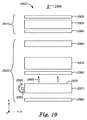
図10は、観察者2999に情報を表示するためのディスプレイシステム2900の概略的側面図である。ディスプレイシステムは、バックライト2920上に配置され、バックライト2920によって照射される、液晶パネル2910を含む。液晶パネル2910は、光吸収型直線偏光子2935と2940との間に配置された液晶セル2930を含む。ディスプレイシステム2900が観測者2999に対して画像を表示する場合のような特定の場合では、液晶パネル2910をピクセル化することができる。
FIG. 10 is a schematic side view of a
バックライト2920は、側方反射体2995内に収容されたランプ2990からライトガイドのエッジを通じて光を受光するライトガイド2970、後方反射体に入射する光を観測者2999の方向に反射するための後方反射体2980、ライトガイドの発光面2975から出射する光2985を均質化するための光学拡散体2960、及び光学拡散体と反射偏光板2950との間に配置された光学積層体2800を備えている。
The
光学積層体2800は1つ以上の構造化光学フィルム100を包含することができる。一部の場合には、2つの構造化光学フィルム100のリニアプリズム構造が相互に直交して配向されている、2つの構造化光学フィルム100が使用される。例えば,図11は、最下部フィルム1120上に配置されたフィルム100に類似の、フィルム100にも類似した最上部フィルム1110の概略側面図である。一部の場合には、フィルム1120の最下部主表面は平滑であってもよい。密充填された微小レンズ160はライトガイド2970と面することができ、プリズム状微小構造物はライトガイドからみて外方に向くことができる。
The
光学積層体2800は、ディスプレイシステムの軸上輝度など輝度を向上させることができる。同時に、光学積層体の密充填された微小レンズ160は、引っ掻き傷などの物理的な欠陥を遮蔽するのに充分に低い光学的透明度を有し、モアレ及び色むらなどの光学的な欠陥を隠蔽するか及び/又は無くし、同時にスパークルを減少させ、又は無くす。
The optical
反射偏光子2950は、第1の偏光状態を有する光を実質的に反射し、第2の偏光状態を有する光を実質的に透過し、この2つの偏光状態は、相互に直交する。例えば、反射偏光子2950によって実質的に反射される偏光状態の可視部における反射偏光子の平均反射率は、少なくとも約50%、又は少なくとも約60%、又は少なくとも約70%、又は少なくとも約80%、又は少なくとも約90%、又は少なくとも約95%である。別の例として、反射偏光子2950によって実質的に透過される偏光状態の可視部における反射偏光子の平均透過率は、少なくとも約50%、又は少なくとも約60%、又は少なくとも約70%、又は少なくとも約80%、又は少なくとも約90%、又は少なくとも約95%、又は少なくとも約97%、又は少なくとも約98%、又は少なくとも約99%である。一部の場合、反射偏光子2950は、第1の直線偏光状態を有する光を(例えば、x方向に沿って)実質的に反射し、第2の直線偏光状態を有する光を(例えば、y方向に沿って)実質的に透過する。
The
反射偏光層2950には、任意の好適な種類の反射偏光子、例えば、多層光学フィルム(MOF)反射偏光子、3M Company(St.Paul,Minnesota)から入手可能なVikuiti(商標)などの拡散反射性偏光子フィルム(「DRPF」)などの連続相及び分散相を有する拡散反射偏光フィルム(DRPF)、例えば米国特許第6,719,426号に記載されるワイヤグリッド反射偏光子、又はコレステリック反射偏光子などを用いてもよい。
The reflective
例えば、一部の場合、反射偏光子2950は、異なるポリマー材料の交互層で形成されるMOF反射偏光子であるか、これを含んでよく、一連の交互層のうちの1つは複屈折材料で形成され、異なる材料の屈折率は、1つの直線偏光状態で偏光された光に一致し、直交する直線偏光状態の光には一致しない。このような場合、一致した偏光状態の入射光線は、反射偏光子2950を実質的に透過し、一致しない偏光状態の入射光線は、反射偏光子2950によって実質的に反射される。一部の場合、MOF反射偏光子2950は、無機誘電体層の積層体を含んでよい。
For example, in some cases, the
別の例として、反射偏光子2950は、通過状態で中間軸上平均反射率を有する部分反射層であるか、これを含んでよい。例えば、部分反射層は、xy平面などの第1の平面にて偏光された可視光に対して、少なくとも約90%の軸上平均反射率を、また第1の平面に垂直な、xz平面などの第2の平面にて偏光された可視光に対して、約25%〜約90%の範囲の軸上平均反射率を有することができる。このような部分反射層は、例えば、その開示は参照によりその全てが本明細書に組み込まれる、米国特許出願第2008/064133号に記載されている。
As another example, the
一部の場合、反射偏光子2950は、円反射偏光子であるか、これを含んでよく、一方向(時計回り又は反時計回りの方向であってもよく、右円偏光又は左円偏光とも呼ばれる)に円偏光された光が優先的に透過され、反対の方向に偏光された光は優先的に反射される。円偏光子の1つのタイプは、コレステリック液晶偏光子を含む。
In some cases, the
一部の場合、反射偏光板2950は、例えば、いずれも全体で本明細書に組み込まれている、2009年11月19日出願の米国仮特許出願第61/116132号、2008年11月19日出願の米国仮特許出願第61/116291号、2008年11月19日出願の米国仮特許出願第61/116294号、2008年11月19日出願の米国仮特許出願第61/116295号、2008年11月19日出願の米国仮特許出願第61/116295号、及び、200年4月15日(April 15, 200)出願の米国仮特許出願第60/939085号に基づく優先権を主張する2008年5月19日出願の国際特許出願第PCT/US 2008/060311号に述べられるものなどの、光学的干渉によって光を反射又は透過する多層光学フィルムであってよい。
In some cases, reflective
光学拡散体2960は、ランプ2990を隠蔽又は遮蔽し、光ガイド2970から放射される光2985を均質化するという主要機能を有する。光学拡散体2960は、高い光学ヘーズ及び/又は高い光学拡散反射率及び/又は透過率有する。例えば、一部の場合、光学拡散体の光学ヘーズは、約40%以上、又は約50%以上、又は約60%以上、又は約70%以上、又は約80%以上、又は約85%以上、又は約90%以上、又は約95%以上である。別の例として、光学拡散体の散乱光反射率は、約30%以上、又は約40%以上、又は約50%以上、又は約60%以上である。
The
光学拡散体2960は、用途において望ましい可能性のある、及び/又は使用可能である光学拡散体であるか、これを含んでよい。例えば、光学拡散体2960は、表面拡散体、体積拡散体、又はこれらの組み合わせであるか、これを含んでよい。例えば、光学拡散体2960は、結合剤中に分散された第1の屈折率n1を有する複数の粒子、又は異なる屈折率n2を有するホスト媒質を含んでよく、2つの屈折率の差は、少なくとも約0.01、又は少なくとも約0.02、又は少なくとも約0.03、又は少なくとも約0.04、又は少なくとも約0.05である。
The
後方反射体2980は、負のz方向に沿って観察者2999から離れる方向に光ガイドによって放射される光を受け取り、受け取った光を観察者に向けて反射する。ランプ2990が光ガイドのエッジに沿って配置されたディスプレイシステム2900などのディスプレイシステムは、一般に、エッジライト又はバックライトディスプレイ又は光学システムと呼ばれる。一部の場合、後方反射体は部分的に反射性であり、部分的に透過性であってよい。特定の場合では、後方反射体は例えば構造化表面を有するように構造化することができる。
The back reflector 2980 receives light emitted by the light guide in a direction away from the
後方反射体2980は、用途において望ましい及び/又は実用的である可能性がある任意の種類の反射体であってよい。例えば、後方反射体は、いずれも参照として全体で本明細書に組み込まれている、2007年5月20日出願の米国特許仮出願第60/939085号からの優先権を主張している、2008年5月19日出願の国際特許出願第PCT/US 2008/064115号に開示されているものなどの、鏡面反射体、半鏡面又は半拡散反射体又は拡散反射体であることができる。例えば、反射体は、アルミ被覆したフィルム又は増強された鏡面反射体(ESR)フィルム(3M Company(St.Paul,MN)から入手可能)などの多層ポリマー反射性フィルムであることができる。別の例としては、後方反射体2980は、白色の外観を有する拡散反射体とすることができる。 The back reflector 2980 may be any type of reflector that may be desirable and / or practical in the application. For example, the back reflector claims priority from US Provisional Application No. 60/939085, filed May 20, 2007, both of which are hereby incorporated by reference in their entirety. 2008 It can be a specular reflector, a semi-specular or a semi-diffuse reflector or a diffuse reflector, such as those disclosed in International Patent Application No. PCT / US 2008/064115 filed 19 May. For example, the reflector can be a multilayer polymer reflective film, such as an aluminum coated film or an enhanced specular reflector (ESR) film (available from 3M Company (St. Paul, MN)). As another example, the back reflector 2980 can be a diffuse reflector having a white appearance.
本明細書で使用するところの「垂直」、「水平」、「上方」、「下方」、「左」、「右」、「上側」及び「下側」、「時計回り」及び「反時計回り」などの用語、並びに他の同様の用語は、図に示される相対的な位置を示す。広くは、物理的実施形態は異なる配向を有することができ、その場合、用語は、装置の実際の配向に修正された相対位置を意味するように意図されている。例えば、図1の画像が図の配向と比べて反転していても、第1の主表面110は、最上部の主表面であると見なされる。
As used herein, “vertical”, “horizontal”, “upper”, “lower”, “left”, “right”, “upper” and “lower”, “clockwise” and “counterclockwise” As well as other similar terms indicate the relative positions shown in the figures. Broadly speaking, the physical embodiments can have different orientations, in which case the term is intended to mean a relative position modified to the actual orientation of the device. For example, even if the image of FIG. 1 is inverted compared to the orientation of the figure, the first
開示されたシステム及び構造物の利点の幾つかは、以下の実施例によって更に説明される。この実施例で列挙される特定の材料、量及び寸法、並びに他の条件及び詳細は、本発明を不当に制限するものと解釈されるべきではない。 Some of the advantages of the disclosed systems and structures are further illustrated by the following examples. The specific materials, amounts and dimensions listed in this example, as well as other conditions and details, should not be construed to unduly limit the present invention.
5.4μmのマシンピッチを使用して国際特許出願第PCT/US 2010/036018号で以前に記述されたカッティングツールシステムにより作製したパターンを付けたロールを用いて、50μm厚のポリエチレンテレフタレート(PET)基板上で微小複製することにより、マットコーティング付きフィルム(実施例A)を作製した。フィルム(ほぼ400μm×400μm)からの試料(実施例A)の顕微鏡写真を図3に示す。 50 μm thick polyethylene terephthalate (PET) using a patterned roll made with a cutting tool system previously described in International Patent Application No. PCT / US 2010/036018 using a machine pitch of 5.4 μm A film with a mat coating (Example A) was produced by micro-replication on a substrate. A photomicrograph of a sample (Example A) from a film (approximately 400 μm × 400 μm) is shown in FIG.
次いで、図1に示す表面(密充填された微小レンズ)のキャラクタリゼーションを行った。最初に、原子間力顕微鏡(AFM)を使用して、試料の高さマップを作製した。同定した各ピーク領域に対して、面積、横方向寸法及び高さを、MATLAB画像解析ソフトウエア(The MathWorks Inc.(Natick MA)から入手可能)を用いて測定した。この試料のピーク領域に対する平均面積は約331平方μmであった。平均の最大の横方向寸法は約29μmであり、平均の最小の横方向寸法は約16μmであった。試料(実施例A)に対する最大の横方向寸法の累積分布を図4に示す。 Next, the surface (closely packed microlens) shown in FIG. 1 was characterized. First, an atomic force microscope (AFM) was used to create a sample height map. For each identified peak region, the area, lateral dimensions and height were measured using MATLAB image analysis software (available from The MathWorks Inc. (Natick MA)). The average area with respect to the peak region of this sample was about 331 square μm. The average maximum lateral dimension was about 29 μm and the average minimum lateral dimension was about 16 μm. The cumulative distribution of the maximum lateral dimension for the sample (Example A) is shown in FIG.
実施例Aに対して最小及び最大ピーク高さも測定した。最大ピーク高さをピーク領域内の最大z値からマイナスピーク領域の周辺上の最小z値として計算した。最小ピーク高さをピーク領域中の最大z値マイナスピーク領域の周辺上の最大z値として計算した。次いで、平均ピーク高さは、ピーク領域中の最大z値マイナスピーク領域の周辺上の平均z値であった。平均ピーク高さの最大は約0.7μmであり、平均ピーク高さの最小は約0.1μmであった。実施例Aに対する平均ピーク高さの累積分布を図5に示し、実施例Aに対する最大ピーク高さの累積分布を図6に示す。 Minimum and maximum peak heights were also measured for Example A. The maximum peak height was calculated as the minimum z value on the periphery of the minus peak region from the maximum z value in the peak region. The minimum peak height was calculated as the maximum z value in the peak area minus the maximum z value on the periphery of the peak area. The average peak height was then the maximum z value in the peak region minus the average z value on the periphery of the peak region. The maximum average peak height was about 0.7 μm and the minimum average peak height was about 0.1 μm. The cumulative distribution of average peak height for Example A is shown in FIG. 5, and the cumulative distribution of maximum peak height for Example A is shown in FIG.
実施例Aに対するピーク領域の円相当径(ECD)を、与えられた領域と同一の面積を有する円の直径として求めた。示される試料(実施例A)に対しては、試料のピーク領域の平均ECDはほぼ19μmであった。試料(実施例A)に対するECDの累積分布を図7に示す。 The equivalent circle diameter (ECD) of the peak region for Example A was determined as the diameter of a circle having the same area as the given region. For the sample shown (Example A), the average ECD of the sample peak area was approximately 19 μm. The cumulative distribution of ECD for the sample (Example A) is shown in FIG.
ピーク領域により定義される微小レンズの代表的な集合に対して光学顕微鏡を用いて焦点距離を測定した。手順は、各微小レンズ中に遠い点源を描き、次いで微小レンズの焦点と微小レンズ表面との間の距離を測定した。最初に、顕微鏡を、広い光源開口を用いて、全微小レンズを照明して微小レンズのエッジ上に焦点を合わせた。次いで、狭い光源開口に切り替えて、微小レンズの焦点が見えるまで顕微鏡ステージを持ち上げた。焦点の長さはステージを持ち上げた距離であった。この試料(実施例A)に対しては、焦点の長さはほぼ184μmであった。 The focal length was measured using an optical microscope for a representative set of microlenses defined by the peak area. The procedure drew a distant point source in each microlens and then measured the distance between the microlens focus and the microlens surface. Initially, the microscope was focused on the edge of the microlens by illuminating the entire microlens using a wide light source aperture. Next, the microscope stage was lifted until the focus of the microlens was visible by switching to a narrow light source aperture. The focal length was the distance the stage was lifted. For this sample (Example A), the focal length was approximately 184 μm.
次に、実質的にコリメートした光を用いて試料を照明して、図8に示す画像を生成させた。MATLAB画像解析ソフトウエアを用いて、焦点(図8中の最高強度の点)の間の距離を測定して、各焦点に対して最近隣までの距離を求めた。最近隣の焦点距離の累積分布を図9に示す。平均の最近隣の焦点距離は約18μmであった。 Next, the sample was illuminated with substantially collimated light to generate the image shown in FIG. Using MATLAB image analysis software, the distance between the focal points (the highest intensity points in FIG. 8) was measured to determine the distance to the nearest neighbor for each focal point. FIG. 9 shows the cumulative distribution of the nearest focal lengths. The average nearest focal length was about 18 μm.
次いで、BYK−GardinerからのHaze−Gard Plusヘーズメーターを用いて、フィルムのヘーズを測定し、6%であることを見出した。 The haze of the film was then measured using a Haze-Gard Plus haze meter from BYK-Gardiner and found to be 6%.
このように、構造化光学フィルムの実施形態を開示する。当業者は、本明細書に記載される光学フィルム及びフィルム物品は、開示の実施形態以外の実施形態と共に実施され得ることを認識するであろう。開示された実施形態は、例証するために提示されるもので、制限するためのものではない。 Thus, an embodiment of a structured optical film is disclosed. Those skilled in the art will recognize that the optical films and film articles described herein can be implemented with embodiments other than those disclosed. The disclosed embodiments are presented for purposes of illustration and not limitation.
次は、本開示による代表的な実施形態である。
項目1.光学フィルムであって、
同一の第1の方向に沿って延在する複数のリニアプリズムを備える第1の構造化主表面;及び
複数の密充填された微小レンズを備える対向する第2の構造化主表面を備え、各微小レンズが、最大の横方向寸法D、円相当径ECD及び焦点に対応する有限の焦点の長さfを有し、複数の密充填された微小レンズが、平均の最大の横方向寸法Davg、平均の円相当径ECDavg及び平均の焦点の長さfavgを有し、ECDavg/favgが約0.05〜約0.20の範囲にあり、Davgが約50μm未満であり、前記第2の構造化主表面の約30%未満が約5度よりも大きい勾配の大きさを有する、光学フィルム。
The following are representative embodiments according to the present disclosure.
A first structured major surface comprising a plurality of linear prisms extending along the same first direction; and an opposing second structured major surface comprising a plurality of closely packed microlenses, each The microlenses have a maximum lateral dimension D, an equivalent circle diameter ECD and a finite focal length f corresponding to the focal point, and a plurality of closely packed microlenses have an average maximum lateral dimension D avg. Having an average equivalent circle diameter ECD avg and an average focal length f avg , ECD avg / f avg being in the range of about 0.05 to about 0.20, and D avg being less than about 50 μm; An optical film wherein less than about 30% of the second structured major surface has a gradient magnitude greater than about 5 degrees.
項目2.第2の構造化主表面の少なくとも90%が、前記微小レンズにより覆われている、項目1に記載の光学フィルム。
項目3.第2の構造化主表面の少なくとも94%が、前記微小レンズにより覆われている、項目1に記載の光学フィルム。
項目4.第2の構造化主表面の少なくとも98%が、前記微小レンズにより覆われている、項目1に記載の光学フィルム。
項目5.第2の構造化主表面の少なくとも99%が、前記微小レンズにより覆われている、項目1に記載の光学フィルム。
項目6.ECDavg/favgが、約0.05〜約0.19の範囲にある、項目1に記載の光学フィルム。
項目7.ECDavg/favgが、約0.06〜約0.19の範囲にある、項目1に記載の光学フィルム。
Item 7. ECD avg / f avg is in the range of about 0.06 to about 0.19, an optical film of
項目8.ECDavg/favgが、約0.06〜約0.18の範囲にある、項目1に記載の光学フィルム。
項目9.ECDavg/favgが、約0.07〜約0.18の範囲にある、項目1に記載の光学フィルム。
Item 9. ECD avg / f avg is in the range of about 0.07 to about 0.18, an optical film of
項目10.Davgが、約45μm未満である、項目1に記載の光学フィルム。
項目11.Davgが、約40μm未満である、項目1に記載の光学フィルム。
Item 11. 2. The optical film of
項目12.複数の密充填された微小レンズ中の前記微小レンズの少なくとも80%が、約50μm未満の最大の横方向寸法Dを有する、項目1に記載の光学フィルム。
項目13.複数の密充填された微小レンズ中の前記微小レンズの少なくとも80%が、約45μm未満の最大の横方向寸法Dを有する、項目1に記載の光学フィルム。
Item 13. 2. The optical film of
項目14.複数の密充填された微小レンズ中の前記微小レンズの少なくとも80%が、約40μm未満の最大の横方向寸法Dを有する、項目1に記載の光学フィルム。
項目15.複数の密充填された微小レンズ中の前記微小レンズの少なくとも40%が、約32μm未満の最大の横方向寸法Dを有する、項目1に記載の光学フィルム。
Item 15. The optical film of
項目16.複数の密充填された微小レンズ中の前記微小レンズの少なくとも20%が、約24μm未満の最大の横方向寸法Dを有する、項目1に記載の光学フィルム。
Item 16. The optical film of
項目17.前記第2の構造化主表面の約20%未満が、約5度よりも大きい勾配の大きさを有する、項目1に記載の光学フィルム。
Item 17. The optical film of
項目18.前記第2の構造化主表面の約15%未満が、約5度よりも大きい勾配の大きさを有する、項目1に記載の光学フィルム。
Item 18. The optical film of
項目19.前記第2の構造化主表面の約10%未満が、約5度よりも大きい勾配の大きさを有する、項目1に記載の光学フィルム。
Item 19. The optical film of
項目20.前記第2の構造化主表面の約40%未満が、約4度よりも大きい勾配の大きさを有する、項目1に記載の光学フィルム。
項目21前記第2の構造化主表面の約30%未満が、約4度よりも大きい勾配の大きさを有する、項目1に記載の光学フィルム。
Item 21. The optical film of
項目22.前記第2の構造化主表面の約25%未満が、約4度よりも大きい勾配の大きさを有する、項目1に記載の光学フィルム。
Item 22. The optical film of
項目24.前記第2の構造化主表面の約50%未満が、約3度よりも大きい勾配の大きさを有する、項目1に記載の光学フィルム。
Item 24. The optical film of
項目25.前記第2の構造化主表面の約45%未満が、約3度よりも大きい勾配の大きさを有する、項目1に記載の光学フィルム。
Item 25. The optical film of
項目26前記第2の構造化主表面の約40%未満が、約3度よりも大きい勾配の大きさを有する、項目1に記載の光学フィルム。
Item 26. The optical film of
項目27.前記第2の構造化主表面の約80%未満が、約2度よりも大きい勾配の大きさを有する、項目1に記載の光学フィルム。
Item 27. The optical film of
項目28.前記第2の構造化主表面の約70%未満が、約2度よりも大きい勾配の大きさを有する、項目1に記載の光学フィルム。
Item 28. 2. The optical film of
項目29.前記第2の構造化主表面の約65%未満が、約2度よりも大きい勾配の大きさを有する、項目1に記載の光学フィルム。
Item 29. The optical film of
項目30.複数の微小レンズ中の前記微小レンズの少なくとも80%が、約27μm未満である円相当径ECDを有する、項目1に記載の光学フィルム。
項目31.複数の微小レンズ中の前記微小レンズの少なくとも40%が、約20μm未満である円相当径ECDを有する、項目1に記載の光学フィルム。
Item 31.
項目32.複数の微小レンズ中の前記微小レンズの少なくとも20%が、約14μm未満である円相当径ECDを有する、項目1に記載の光学フィルム。
Item 32.
項目33.複数の微小レンズ中の前記微小レンズの少なくとも90%が、約1.5μm未満であるピーク高さを有する、項目1に記載の光学フィルム。
Item 33. 2. The optical film of
項目34.複数の微小レンズ中の前記微小レンズの少なくとも80%が、約1.2μm未満であるピーク高さを有する、項目1に記載の光学フィルム。
Item 34. The optical film of
項目35.複数の微小レンズ中の前記微小レンズの少なくとも40%が、約0.7μm未満であるピーク高さを有する、項目1に記載の光学フィルム。
Item 35. The optical film of
項目36.複数の微小レンズ中の前記微小レンズの少なくとも90%が、約30μm未満である最近隣の焦点距離を有する、項目1に記載の光学フィルム。
Item 36. 2. The optical film of
項目37.複数の微小レンズ中の前記微小レンズの少なくとも90%が、約25μm未満である最近隣の焦点距離を有する、項目1に記載の光学フィルム。
Item 37. The optical film of
項目38.複数の微小レンズ中の前記微小レンズの少なくとも40%が、約18μm未満である最近隣の焦点距離を有する、項目1に記載の光学フィルム。
Item 38. 2. The optical film of
項目39.複数の微小レンズ中の前記微小レンズの少なくとも20%が、約15μm未満である最近隣の焦点距離を有する、項目1に記載の光学フィルム。
Item 39. The optical film of
項目40.前記第2の構造化主表面が、約3%〜約25%の範囲の光学ヘーズを有する、項目1に記載の光学フィルム。
項目41.前記第2の構造化主表面が、約5%〜約20%の範囲の光学ヘーズを有する、項目1に記載の光学フィルム。
Item 41. The optical film of
項目42.favgが、約250μm未満である、項目1に記載の光学フィルム。
Item 42.
項目43.favgが、約225μm未満である、項目1に記載の光学フィルム。
Item 43.
項目44.favgが、約200μm未満である、項目1に記載の光学フィルム。
Item 44. Item 5. The optical film of
項目45.前記光学フィルムの平均の有効透過率が、前記第2の主表面が構造化されていないことを除いて同一の構成を有する光学フィルムと比べて、同じか高い、又は低く、その差は約10%以下である、項目1に記載の光学フィルム。
Item 45. The average effective transmittance of the optical film is the same or higher or lower than that of the optical film having the same configuration except that the second main surface is not structured, and the difference is about 10
項目46.少なくとも1.3の平均の有効透過率を有する、項目1に記載の光学フィルム。
Item 46.
項目47.前記第2の構造化主表面が、第1の方向に第1の視角AHをもって及び第1の方向と直交する第2の方向にAHに実質的に等しい第2の視角AVをもって光を散乱する、項目1に記載の光学フィルム。
Item 47. Said second structured major surface, with a substantially equal second viewing angle A V in the second direction to the A H orthogonal to the first direction with a first viewing angle A H and a first direction the
項目48.AVとAHとの差異が、10度未満である、項目47に記載の光学フィルム。 Item 48. Difference between A V and A H is less than 10 degrees, the optical film of claim 47.
項目49.前記第2の構造化主表面が、第1の方向に第1の視角AHをもって及び第1の方向と直交する第2の方向にAHに実質的に等しい第2の視角AVをもって光を散乱する、項目1に記載の光学フィルム。
Item 49. Said second structured major surface, with a substantially equal second viewing angle A V in the second direction to the A H orthogonal to the first direction with a first viewing angle A H and a first direction the
項目50.AVとAHとの差異が、15度超である、項目49に記載の光学フィルム。
項目51.第1の方向と異なる同一の第2の方向に沿って延在する複数のを含む導光フィルム上に配置された項目1に記載の光学フィルムを含む光学積層体。
Item 51. The optical laminated body containing the optical film of the
項目52.反射型偏光子を更に含み、項目1に記載の光学フィルムが、前記反射型偏光子と前記導光フィルムとの間に配置される、項目51に記載の光学積層体。
Item 52. Item 52. The optical laminate according to Item 51, further comprising a reflective polarizer, wherein the optical film according to
項目53.前記反射型偏光子層が、交互層を備え、前記交互層の少なくとも1つが複屈折材料を備える、項目52に記載の光学積層体。 Item 53. 53. The optical stack of item 52, wherein the reflective polarizer layer comprises alternating layers and at least one of the alternating layers comprises a birefringent material.
項目54.前記反射型偏光子層が、ワイヤグリッド反射型偏光子を備える、項目52に記載の光学積層体。 Item 54. 53. The optical laminate according to item 52, wherein the reflective polarizer layer comprises a wire grid reflective polarizer.
項目55.前記反射型偏光子層が、コレステリック反射型偏光子を備える、項目52に記載の光学積層体。 Item 55. 53. The optical laminate according to item 52, wherein the reflective polarizer layer comprises a cholesteric reflective polarizer.
項目56.前記反射型偏光子層が、複数の実質的に平行な繊維を備え、前記繊維が複屈折材料を備える、項目52に記載の光学積層体。 Item 56. 53. The optical laminate of item 52, wherein the reflective polarizer layer comprises a plurality of substantially parallel fibers, and the fibers comprise a birefringent material.
項目57.前記反射型偏光子層が、拡散反射偏光フィルム(DRPF)を備える、項目52に記載の光学積層体。 Item 57. Item 53. The optical laminate according to Item 52, wherein the reflective polarizer layer comprises a diffuse reflection polarizing film (DRPF).
項目58.光学フィルムであって、
同一の第1の方向に沿って延在する複数のリニアプリズムを備える第1の構造化主表面;及び
複数の密充填された微小レンズを備える対向する第2の構造化主表面を備え、各微小レンズが、円相当径ECD及び焦点に対応する有限の焦点の長さfを有し、複数の密充填された微小レンズが平均の円相当径ECDavg及び平均の焦点の長さfavgを有し、ECDavg/favgが、約0.05〜約0.20の範囲にあり、複数の密充填された微小レンズ中の前記微小レンズの少なくとも90%が、約30μm未満の最近隣の焦点距離を有し、前記第2の構造化主表面の約30%未満が、約5度よりも大きい勾配の大きさを有する、光学フィルム。
Item 58. An optical film,
A first structured major surface comprising a plurality of linear prisms extending along the same first direction; and an opposing second structured major surface comprising a plurality of closely packed microlenses, each The microlenses have an equivalent circle diameter ECD and a finite focal length f corresponding to the focal point, and a plurality of closely packed microlenses have an average equivalent circle diameter ECDavg and an average focal length favg . And ECD avg / f avg is in the range of about 0.05 to about 0.20, and at least 90% of the microlenses in the plurality of closely packed microlenses are adjacent to less than about 30 μm An optical film having a focal length, wherein less than about 30% of the second structured major surface has a gradient magnitude greater than about 5 degrees.
項目59.第2の構造化主表面の少なくとも90%が、前記微小レンズにより覆われている、項目58に記載の光学フィルム。 Item 59. 59. The optical film of item 58, wherein at least 90% of the second structured main surface is covered with the microlenses.
項目60.第2の構造化主表面の少なくとも94%が、前記微小レンズにより覆われている、項目58に記載の光学フィルム。
項目61.第2の構造化主表面の少なくとも98%が、前記微小レンズにより覆われている、項目58に記載の光学フィルム。 Item 61. 59. The optical film of item 58, wherein at least 98% of the second structured main surface is covered with the microlenses.
項目62.第2の構造化主表面の少なくとも99%が、前記微小レンズにより覆われている、項目58に記載の光学フィルム。 Item 62. 59. The optical film of item 58, wherein at least 99% of the second structured main surface is covered with the microlenses.
項目63.ECDavg/favgが、約0.05〜約0.19の範囲にある、項目58に記載の光学フィルム。 Item 63. 59. The optical film of item 58, wherein ECDavg / favg is in the range of about 0.05 to about 0.19.
項目64.ECDavg/favgが、約0.06〜約0.19の範囲にある、項目58に記載の光学フィルム。 Item 64. ECD avg / f avg is in the range of about 0.06 to about 0.19, an optical film of claim 58.
項目65.ECDavg/favgが、約0.06〜約0.18の範囲にある、項目58に記載の光学フィルム。 Item 65. ECD avg / f avg is in the range of about 0.06 to about 0.18, an optical film of claim 58.
項目66.ECDavg/favgが、約0.07〜約0.18の範囲にある、項目58に記載の光学フィルム。 Item 66. ECD avg / f avg is in the range of about 0.07 to about 0.18, an optical film of claim 58.
項目67.Davgが、約50μm未満である、項目58に記載の光学フィルム。 Item 67. 59. The optical film of item 58, wherein D avg is less than about 50 μm.
項目68.Davgが、約45μm未満である、項目58に記載の光学フィルム。 Item 68. 59. The optical film of item 58, wherein D avg is less than about 45 μm.
項目69.Davgが、約40μm未満である、項目58に記載の光学フィルム。 Item 69. 59. The optical film of item 58, wherein D avg is less than about 40 μm.
項目70.複数の微小レンズ中の前記微小レンズの少なくとも80%が、約50μm未満の最大の横方向寸法Dを有する、項目58に記載の光学フィルム。
項目71.複数の微小レンズ中の前記微小レンズの少なくとも80%が、約45μm未満の最大の横方向寸法Dを有する、項目58に記載の光学フィルム。 Item 71. 59. The optical film of item 58, wherein at least 80% of the microlenses in the plurality of microlenses have a maximum lateral dimension D of less than about 45 [mu] m.
項目72.複数の微小レンズ中の前記微小レンズの少なくとも80%が、約40μm未満の最大の横方向寸法Dを有する、項目58に記載の光学フィルム。 Item 72. 59. The optical film of item 58, wherein at least 80% of the microlenses in the plurality of microlenses have a maximum lateral dimension D of less than about 40 [mu] m.
項目73.複数の微小レンズ中の前記微小レンズの少なくとも40%が、約32μm未満の最大の横方向寸法Dを有する、項目58に記載の光学フィルム。 Item 73. 59. The optical film of item 58, wherein at least 40% of the microlenses in the plurality of microlenses have a maximum lateral dimension D of less than about 32 [mu] m.
項目74.複数の微小レンズ中の前記微小レンズの少なくとも20%が、約24μm未満の最大の横方向寸法Dを有する、項目58に記載の光学フィルム。 Item 74. 59. The optical film of item 58, wherein at least 20% of the microlenses in the plurality of microlenses have a maximum lateral dimension D of less than about 24 [mu] m.
項目75.前記第2の構造化主表面の約20%未満が、約5度よりも大きい勾配の大きさを有する、項目58に記載の光学フィルム。 Item 75. 59. The optical film of item 58, wherein less than about 20% of the second structured major surface has a gradient magnitude greater than about 5 degrees.
項目76.前記第2の構造化主表面の約15%未満が、約5度よりも大きい勾配の大きさを有する、項目58に記載の光学フィルム。 Item 76. 59. The optical film of item 58, wherein less than about 15% of the second structured major surface has a gradient magnitude greater than about 5 degrees.
項目77.前記第2の構造化主表面の約10%未満が、約5度よりも大きい勾配の大きさを有する、項目58に記載の光学フィルム。 Item 77. 59. The optical film of item 58, wherein less than about 10% of the second structured major surface has a gradient magnitude greater than about 5 degrees.
項目78.前記第2の構造化主表面の約40%未満が、約4度よりも大きい勾配の大きさを有する、項目58に記載の光学フィルム。 Item 78. 59. The optical film of item 58, wherein less than about 40% of the second structured major surface has a gradient magnitude greater than about 4 degrees.
項目79.前記第2の構造化主表面の約30%未満が、約4度よりも大きい勾配の大きさを有する、項目58に記載の光学フィルム。 Item 79. 59. The optical film of item 58, wherein less than about 30% of the second structured major surface has a gradient magnitude greater than about 4 degrees.
項目80.前記第2の構造化主表面の約25%未満が、約4度よりも大きい勾配の大きさを有する、項目58に記載の光学フィルム。
項目81.前記第2の構造化主表面の約50%未満が、約3度よりも大きい勾配の大きさを有する、項目58に記載の光学フィルム。 Item 81. 59. The optical film of item 58, wherein less than about 50% of the second structured major surface has a gradient magnitude greater than about 3 degrees.
項目82.前記第2の構造化主表面の約45%未満が、約3度よりも大きい勾配の大きさを有する、項目58に記載の光学フィルム。 Item 82. 59. The optical film of item 58, wherein less than about 45% of the second structured major surface has a gradient magnitude greater than about 3 degrees.
項目83.前記第2の構造化主表面の約40%未満が、約3度よりも大きい勾配の大きさを有する、項目58に記載の光学フィルム。 Item 83. 59. The optical film of item 58, wherein less than about 40% of the second structured major surface has a gradient magnitude greater than about 3 degrees.
項目84.前記第2の構造化主表面の約80%未満が、約2度よりも大きい勾配の大きさを有する、項目58に記載の光学フィルム。 Item 84. 59. The optical film of item 58, wherein less than about 80% of the second structured major surface has a gradient magnitude greater than about 2 degrees.
項目85.前記第2の構造化主表面の約70%未満が、約2度よりも大きい勾配の大きさを有する、項目58に記載の光学フィルム。 Item 85. 59. The optical film of item 58, wherein less than about 70% of the second structured major surface has a gradient magnitude greater than about 2 degrees.
項目86.前記第2の構造化主表面の約65%未満が、約2度よりも大きい勾配の大きさを有する、項目58に記載の光学フィルム。 Item 86. 59. The optical film of item 58, wherein less than about 65% of the second structured major surface has a gradient magnitude greater than about 2 degrees.
項目87.複数の微小レンズ中の前記微小レンズの少なくとも80%が、約27μm未満である円相当径ECDを有する、項目58に記載の光学フィルム。 Item 87. 59. The optical film of item 58, wherein at least 80% of the microlenses in the plurality of microlenses have an equivalent circular diameter ECD that is less than about 27 μm.
項目88.複数の微小レンズ中の前記微小レンズの少なくとも40%が、約20μm未満である円相当径ECDを有する、項目58に記載の光学フィルム。 Item 88. 59. The optical film of item 58, wherein at least 40% of the microlenses in the plurality of microlenses have an equivalent circle diameter ECD that is less than about 20 [mu] m.
項目89.複数の微小レンズ中の前記微小レンズの少なくとも20%が、約14μm未満である円相当径ECDを有する、項目58に記載の光学フィルム。 Item 89. 59. The optical film of item 58, wherein at least 20% of the microlenses in the plurality of microlenses have an equivalent circular diameter ECD that is less than about 14 μm.
項目90.複数の微小レンズ中の前記微小レンズの少なくとも90%が、約1.5μm未満であるピーク高さを有する、項目58に記載の光学フィルム。 Item 90. 59. The optical film of item 58, wherein at least 90% of the microlenses in the plurality of microlenses have a peak height that is less than about 1.5 μm.
項目91.複数の微小レンズ中の前記微小レンズの少なくとも80%が、約1.2μm未満であるピーク高さを有する、項目58に記載の光学フィルム。 Item 91. 59. The optical film of item 58, wherein at least 80% of the microlenses in the plurality of microlenses have a peak height that is less than about 1.2 μm.
項目92.複数の微小レンズ中の前記微小レンズの少なくとも40%が、約0.7μm未満であるピーク高さを有する、項目58に記載の光学フィルム。 Item 92. 59. The optical film of item 58, wherein at least 40% of the microlenses in the plurality of microlenses have a peak height that is less than about 0.7 μm.
項目93.複数の微小レンズ中の前記微小レンズの少なくとも90%が、約25μm未満である最近隣の焦点距離を有する、項目58に記載の光学フィルム。 Item 93. 59. The optical film of item 58, wherein at least 90% of the microlenses in the plurality of microlenses have a nearest focal length that is less than about 25 μm.
項目94.複数の微小レンズ中の前記微小レンズの少なくとも40%が、約18μm未満である最近隣の焦点距離を有する、項目58に記載の光学フィルム。 Item 94. 59. The optical film of item 58, wherein at least 40% of the microlenses in the plurality of microlenses have a nearest focal length that is less than about 18 [mu] m.
項目95.複数の微小レンズ中の前記微小レンズの少なくとも20%が、約15μm未満である最近隣の焦点距離を有する、項目58に記載の光学フィルム。 Item 95. 59. The optical film of item 58, wherein at least 20% of the microlenses in the plurality of microlenses have a nearest focal length that is less than about 15 μm.
項目96.前記第2の構造化主表面が、約3%〜約25%の範囲の光学ヘーズを有する、項目58に記載の光学フィルム。 Item 96. 59. The optical film of item 58, wherein the second structured major surface has an optical haze in the range of about 3% to about 25%.
項目97.前記第2の構造化主表面が、約5%〜約20%の範囲の光学ヘーズを有する、項目58に記載の光学フィルム。 Item 97. 59. The optical film of item 58, wherein the second structured major surface has an optical haze in the range of about 5% to about 20%.
項目98.favgが、約250μm未満である、項目58に記載の光学フィルム。 Item 98. 59. The optical film of item 58, wherein f avg is less than about 250 μm.
項目99.favgが、約225μm未満である、項目58に記載の光学フィルム。 Item 99. 59. The optical film of item 58, wherein f avg is less than about 225 μm.
項目100.favgが、約200μm未満である、項目58に記載の光学フィルム。
項目101.前記光学フィルムの平均の有効透過率が、前記第2の主表面が構造化されていないことを除いて同一の構成を有する光学フィルムと比べて、同じか高い、又は低く、その差は約10%以下である、項目58に記載の光学フィルム。 Item 101. The average effective transmittance of the optical film is the same or higher or lower than that of the optical film having the same configuration except that the second main surface is not structured, and the difference is about 10 59. The optical film according to Item 58, which is% or less.
項目102.少なくとも1.3の平均の有効透過率を有する、項目58に記載の光学フィルム。 Item 102. 59. The optical film of item 58, having an average effective transmittance of at least 1.3.
項目103.前記第2の構造化主表面が、第1の方向に第1の視角AHをもって及び第1の方向と直交する第2の方向にAHに実質的に等しい第2の視角AVをもって光を散乱する、項目58に記載の光学フィルム。 Item 103. Said second structured major surface, with a substantially equal second viewing angle A V in the second direction to the A H orthogonal to the first direction with a first viewing angle A H and a first direction the light 59. The optical film according to Item 58, which scatters light.
項目104.AVとAHとの差異が、10度未満である、項目103に記載の光学フィルム。 Item 104. Difference between A V and A H is less than 10 degrees, the optical film of claim 103.
項目105.前記第2の構造化主表面が、第1の方向に第1の視角AHをもって及び第1の方向と直交する第2の方向にAHに実質的に等しい第2の視角AVをもって光を散乱する、項目58に記載の光学フィルム。 Item 105. Said second structured major surface, with a substantially equal second viewing angle A V in the second direction to the A H orthogonal to the first direction with a first viewing angle A H and a first direction the light 59. The optical film according to Item 58, which scatters light.
項目106.AVとAHとの差異が、15度超である、項目105に記載の光学フィルム。 Item 106. Difference between A V and A H is 15 degrees greater than the optical film of claim 105.
項目107.第1の方向と異なる同一の第2の方向に沿って延在する複数のを含む導光フィルム上に配置された項目58に記載の光学フィルムを含む光学積層体。 Item 107. 59. An optical laminate including the optical film according to item 58, which is disposed on a light guide film including a plurality extending along the same second direction different from the first direction.
項目108.反射型偏光子を更に含み、項目58に記載の光学フィルムが、前記反射型偏光子と前記導光フィルムとの間に配置される、項目107に記載の光学積層体。 Item 108. 108. The optical laminate according to item 107, further including a reflective polarizer, wherein the optical film according to item 58 is disposed between the reflective polarizer and the light guide film.
項目109.前記反射型偏光子層が、交互層を備え、前記交互層の少なくとも1つが複屈折材料を備える、項目107に記載の光学積層体。 Item 109. 108. The optical stack of item 107, wherein the reflective polarizer layer comprises alternating layers, and at least one of the alternating layers comprises a birefringent material.
項目110.前記反射型偏光子層が、ワイヤグリッド反射型偏光子を備える、項目107に記載の光学積層体。
項目111.前記反射型偏光子層が、コレステリック反射型偏光子を備える、項目107に記載の光学積層体。 Item 111. 108. The optical laminate according to item 107, wherein the reflective polarizer layer comprises a cholesteric reflective polarizer.
項目112.前記反射型偏光子層が、複数の実質的に平行な繊維を備え、前記繊維が複屈折材料を備える、項目107に記載の光学積層体。 Item 112. 108. The optical laminate of item 107, wherein the reflective polarizer layer comprises a plurality of substantially parallel fibers, and the fibers comprise a birefringent material.
項目113.前記反射型偏光子層が、拡散反射偏光フィルム(DRPF)を備える、項目107に記載の光学積層体。 Item 113. 108. The optical laminate according to item 107, wherein the reflective polarizer layer comprises a diffuse reflection polarizing film (DRPF).
項目114.光学フィルムであって、
同一の第1の方向に沿って延在する複数のリニアプリズムを備える第1の構造化主表面;及び
複数の密充填された微小レンズを備える、対向する第2の構造化主表面と、を備え、各微小レンズが、最大の横方向寸法Dを有し、前記複数の密充填された微小レンズが、平均の最大の横方向寸法Davgを有し、Davgが、約50μm未満であり、前記複数の密充填された微小レンズ中の前記微小レンズの少なくとも90%が、約30μm未満の最近隣の焦点距離を有し、前記第2の構造化主表面の約30%未満が約5度よりも大きい勾配の大きさを有する、光学フィルム。
Item 114. An optical film,
A first structured major surface comprising a plurality of linear prisms extending along the same first direction; and an opposing second structured major surface comprising a plurality of closely packed microlenses. Each microlens has a maximum lateral dimension D, the plurality of closely packed microlenses have an average maximum lateral dimension D avg , and D avg is less than about 50 μm , At least 90% of the microlenses in the plurality of closely packed microlenses have a nearest focal length of less than about 30 μm, and less than about 30% of the second structured major surface is about 5 An optical film having a gradient magnitude greater than degrees.
項目115.第2の構造化主表面の少なくとも90%が、前記微小レンズにより覆われている、項目114に記載の光学フィルム。 Item 115. 115. The optical film of item 114, wherein at least 90% of the second structured main surface is covered by the microlenses.
項目116.第2の構造化主表面の少なくとも94%が、前記微小レンズにより覆われている、項目114に記載の光学フィルム。 Item 116. 115. The optical film of item 114, wherein at least 94% of the second structured main surface is covered by the microlenses.
項目117.第2の構造化主表面の少なくとも98%が、前記微小レンズにより覆われている、項目114に記載の光学フィルム。 Item 117. 115. The optical film of item 114, wherein at least 98% of the second structured main surface is covered by the microlenses.
項目118.第2の構造化主表面の少なくとも99%が、前記微小レンズにより覆われている、項目114に記載の光学フィルム。 Item 118. 115. The optical film of item 114, wherein at least 99% of the second structured main surface is covered by the microlenses.
項目119.Davgが、約45μm未満である、項目114に記載の光学フィルム。 Item 119. 115. The optical film of item 114, wherein D avg is less than about 45 μm.
項目120.Davgが、約40μm未満である、項目114に記載の光学フィルム。
項目121.複数の微小レンズ中の前記微小レンズの少なくとも80%が、約50μm未満の最大の横方向寸法Dを有する、項目114に記載の光学フィルム。 Item 121. 115. The optical film of item 114, wherein at least 80% of the microlenses in the plurality of microlenses have a maximum lateral dimension D of less than about 50 μm.
項目122.複数の微小レンズ中の前記微小レンズの少なくとも80%が、約45μm未満の最大の横方向寸法Dを有する、項目114に記載の光学フィルム。 Item 122. 115. The optical film of item 114, wherein at least 80% of the microlenses in the plurality of microlenses have a maximum lateral dimension D of less than about 45 μm.
項目123.複数の微小レンズ中の前記微小レンズの少なくとも80%が、約40μm未満の最大の横方向寸法Dを有する、項目114に記載の光学フィルム。 Item 123. 115. The optical film of item 114, wherein at least 80% of the microlenses in the plurality of microlenses have a maximum lateral dimension D of less than about 40 μm.
項目124.複数の微小レンズ中の前記微小レンズの少なくとも40%が、約32μm未満の最大の横方向寸法Dを有する、項目114に記載の光学フィルム。 Item 124. 115. The optical film of item 114, wherein at least 40% of the microlenses in the plurality of microlenses have a maximum lateral dimension D of less than about 32 μm.
項目125.複数の微小レンズ中の前記微小レンズの少なくとも20%が、約24μm未満の最大の横方向寸法Dを有する、項目114に記載の光学フィルム。 Item 125. 115. The optical film of item 114, wherein at least 20% of the microlenses in the plurality of microlenses have a maximum lateral dimension D of less than about 24 μm.
項目126.前記第2の構造化主表面の約20%未満が、約5度よりも大きい勾配の大きさを有する、項目114に記載の光学フィルム。 Item 126. 115. The optical film of item 114, wherein less than about 20% of the second structured major surface has a gradient magnitude greater than about 5 degrees.
項目127.前記第2の構造化主表面の約15%未満が、約5度よりも大きい勾配の大きさを有する、項目114に記載の光学フィルム。 Item 127. 115. The optical film of item 114, wherein less than about 15% of the second structured major surface has a gradient magnitude greater than about 5 degrees.
項目128.前記第2の構造化主表面の約10%未満が、約5度よりも大きい勾配の大きさを有する、項目114に記載の光学フィルム。 Item 128. 115. The optical film of item 114, wherein less than about 10% of the second structured major surface has a gradient magnitude greater than about 5 degrees.
項目129.前記第2の構造化主表面の約40%未満が、約4度よりも大きい勾配の大きさを有する、項目114に記載の光学フィルム。 Item 129. 115. The optical film of item 114, wherein less than about 40% of the second structured major surface has a gradient magnitude greater than about 4 degrees.
項目130.前記第2の構造化主表面の約30%未満が、約4度よりも大きい勾配の大きさを有する、項目114に記載の光学フィルム。
項目131.前記第2の構造化主表面の約25%未満が、約4度よりも大きい勾配の大きさを有する、項目114に記載の光学フィルム。 Item 131. 115. The optical film of item 114, wherein less than about 25% of the second structured major surface has a gradient magnitude greater than about 4 degrees.
項目132.前記第2の構造化主表面の約50%未満が、約3度よりも大きい勾配の大きさを有する、項目114に記載の光学フィルム。 Item 132. 115. The optical film of item 114, wherein less than about 50% of the second structured major surface has a gradient magnitude greater than about 3 degrees.
項目133.前記第2の構造化主表面の約45%未満が、約3度よりも大きい勾配の大きさを有する、項目114に記載の光学フィルム。 Item 133. 115. The optical film of item 114, wherein less than about 45% of the second structured major surface has a gradient magnitude greater than about 3 degrees.
項目134.前記第2の構造化主表面の約40%未満が、約3度よりも大きい勾配の大きさを有する、項目114に記載の光学フィルム。 Item 134. 115. The optical film of item 114, wherein less than about 40% of the second structured major surface has a gradient magnitude greater than about 3 degrees.
項目135.前記第2の構造化主表面の約80%未満が、約2度よりも大きい勾配の大きさを有する、項目114に記載の光学フィルム。 Item 135. 115. The optical film of item 114, wherein less than about 80% of the second structured major surface has a gradient magnitude greater than about 2 degrees.
項目136.前記第2の構造化主表面の約70%未満が、約2度よりも大きい勾配の大きさを有する、項目114に記載の光学フィルム。 Item 136. 115. The optical film of item 114, wherein less than about 70% of the second structured major surface has a gradient magnitude greater than about 2 degrees.
項目137.前記第2の構造化主表面の約65%未満が、約2度よりも大きい勾配の大きさを有する、項目114に記載の光学フィルム。 Item 137. 115. The optical film of item 114, wherein less than about 65% of the second structured major surface has a gradient magnitude greater than about 2 degrees.
項目138.複数の微小レンズ中の前記微小レンズの少なくとも90%が、約25μm未満である最近隣の焦点距離を有する、項目114に記載の光学フィルム。 Item 138. 115. The optical film of item 114, wherein at least 90% of the microlenses in the plurality of microlenses have a nearest focal length that is less than about 25 μm.
項目139.複数の微小レンズ中の前記微小レンズの少なくとも40%が、約18μm未満である最近隣の焦点距離を有する、項目114に記載の光学フィルム。 Item 139. 115. The optical film of item 114, wherein at least 40% of the microlenses in the plurality of microlenses have a nearest focal length that is less than about 18 μm.
項目140.複数の微小レンズ中の前記微小レンズの少なくとも20%が、約15μm未満である最近隣の焦点距離を有する、項目114に記載の光学フィルム。
項目141.各微小レンズが、円相当径ECD及び焦点に対応する有限の焦点の長さfを有し、複数の密充填された微小レンズが、平均の円相当径ECDavg及び平均の焦点の長さfavgを有し、ECDavg/favgが、約0.05〜約0.20の範囲にある、項目114に記載の光学フィルム。 Item 141. Each microlens has an equivalent circular diameter ECD and a finite focal length f corresponding to the focal point, and a plurality of closely packed microlenses have an average equivalent circular diameter ECD avg and an average focal length f. 115. The optical film of item 114, having avg and having an ECD avg / f avg in the range of about 0.05 to about 0.20.
項目142.ECDavg/favgが、約0.05〜約0.19の範囲にある、項目141に記載の光学フィルム。
項目143.ECDavg/favgが、約0.06〜約0.19の範囲にある、項目141に記載の光学フィルム。 Item 143. ECD avg / f avg is in the range of about 0.06 to about 0.19, an optical film of claim 141.
項目144.ECDavg/favgが、約0.06〜約0.18の範囲にある、項目141に記載の光学フィルム。 Item 144. ECD avg / f avg is in the range of about 0.06 to about 0.18, an optical film of claim 141.
項目145.ECDavg/favgが、約0.07〜約0.18の範囲にある、項目141に記載の光学フィルム。 Item 145. ECD avg / f avg is in the range of about 0.07 to about 0.18, an optical film of claim 141.
項目145.複数の微小レンズ中の前記微小レンズの少なくとも80%が、約27μm未満である円相当径ECDを有する、項目141に記載の光学フィルム。 Item 145. 142. The optical film of item 141, wherein at least 80% of the microlenses in the plurality of microlenses have an equivalent circle diameter ECD that is less than about 27 μm.
項目146.複数の微小レンズ中の前記微小レンズの少なくとも40%が、約20μm未満である円相当径ECDを有する、項目141に記載の光学フィルム。 Item 146. 142. The optical film of item 141, wherein at least 40% of the microlenses in the plurality of microlenses have a circle-equivalent diameter ECD that is less than about 20 μm.
項目147.複数の微小レンズ中の前記微小レンズの少なくとも20%が、約14μm未満である円相当径ECDを有する、項目141に記載の光学フィルム。 Item 147. 142. The optical film of item 141, wherein at least 20% of the microlenses in the plurality of microlenses have an equivalent circle diameter ECD that is less than about 14 μm.
項目148.複数の微小レンズ中の前記微小レンズの少なくとも90%が、約1.5μm未満であるピーク高さを有する、項目114に記載の光学フィルム。 Item 148. 115. The optical film of item 114, wherein at least 90% of the microlenses in the plurality of microlenses have a peak height that is less than about 1.5 μm.
項目149.複数の微小レンズ中の前記微小レンズの少なくとも80%が、約1.2μm未満であるピーク高さを有する、項目114に記載の光学フィルム。 Item 149. 115. The optical film of item 114, wherein at least 80% of the microlenses in the plurality of microlenses have a peak height that is less than about 1.2 μm.
項目150.複数の微小レンズ中の前記微小レンズの少なくとも40%が、約0.7μm未満であるピーク高さを有する、項目114に記載の光学フィルム。
項目151.前記第2の構造化主表面が、約3%〜約25%の範囲の光学ヘーズを有する、項目114に記載の光学フィルム。
項目152.前記第2の構造化主表面が、約5%〜約20%の範囲の光学ヘーズを有する、項目114に記載の光学フィルム。
項目153.favgが、約250μm未満である、項目141に記載の光学フィルム。
項目154favgが、約225μm未満である、項目141に記載の光学フィルム。 142. The optical film of item 141, wherein item 154f avg is less than about 225 μm.
項目155.favgが、約200μm未満である、項目141に記載の光学フィルム。
項目156.前記光学フィルムの平均の有効透過率が、前記第2の主表面が構造化されていないことを除いて同一の構成を有する光学フィルムと比べて、同じか高い、又は低く、その差は約10%以下である、項目114に記載の光学フィルム。
項目157.少なくとも1.3の平均の有効透過率を有する、項目114に記載の光学フィルム。
項目158.前記第2の構造化主表面が、第1の方向に第1の視角AHをもって及び第1の方向と直交する第2の方向にAHに実質的に等しい第2の視角AVをもって光を散乱する、項目114に記載の光学フィルム。
項目159.AVとAHとの差異が、10度未満である、項目158に記載の光学フィルム。
Item 159. Difference between A V and A H is less than 10 degrees, the optical film of
項目160.前記第2の構造化主表面が、第1の方向に第1の視角AHをもって及び第1の方向と直交する第2の方向にAHに実質的に等しい第2の視角AVをもって光を散乱する、項目114に記載の光学フィルム。
項目161.AVとAHとの差異が、15度超である、項目160に記載の光学フィルム。
Item 161. Difference between A V and A H is 15 degrees greater than the optical film of
項目162.第1の方向と異なる同一の第2の方向に沿って延在する複数のを含む導光フィルム上に配置された項目114に記載の光学フィルムを含む光学積層体。 Item 162. 115. An optical laminate including the optical film according to item 114, which is disposed on a light guide film including a plurality extending along the same second direction different from the first direction.
項目163.反射型偏光子を更に含み、項目114に記載の光学フィルムが、前記反射型偏光子と前記導光フィルムとの間に配置される、項目162に記載の光学積層体。 Item 163. 163. The optical laminate according to item 162, further including a reflective polarizer, wherein the optical film according to item 114 is disposed between the reflective polarizer and the light guide film.
項目164.前記反射型偏光子層が、交互層を備え、前記交互層の少なくとも1つが複屈折材料を備える、項目162に記載の光学積層体。 Item 164. 163. The optical stack of item 162, wherein the reflective polarizer layer comprises alternating layers and at least one of the alternating layers comprises a birefringent material.
項目165.前記反射型偏光子層が、ワイヤグリッド反射型偏光子を備える、項目162に記載の光学積層体。 Item 165. 163. An optical laminate according to item 162, wherein the reflective polarizer layer comprises a wire grid reflective polarizer.
項目166.前記反射型偏光子層が、コレステリック反射型偏光子を備える、項目162に記載の光学積層体。 Item 166. 163. An optical laminate according to item 162, wherein the reflective polarizer layer comprises a cholesteric reflective polarizer.
項目167.前記反射型偏光子層が、複数の実質的に平行繊維を備え、前記繊維が複屈折材料を備える、項目162に記載の光学積層体。 Item 167. 163. An optical laminate according to item 162, wherein the reflective polarizer layer comprises a plurality of substantially parallel fibers, and the fibers comprise a birefringent material.
項目168.前記反射型偏光子層が、拡散反射偏光フィルム(DRPF)を備える、項目162に記載の光学積層体。本発明の実施態様の一部を以下の項目[1]−[10]に記載する。
[1]
光学フィルムであって、
同一の第1の方向に沿って延在する複数のリニアプリズムを備える第1の構造化主表面と、
複数の密充填された微小レンズを備える、対向する第2の構造化主表面と、を備え、各微小レンズが、最大の横方向寸法D、円相当径ECD及び焦点に対応する有限の焦点の長さfを有し、前記複数の密充填された微小レンズが、平均の最大の横方向寸法D avg 、平均の円相当径ECD avg 及び平均の焦点の長さf avg を有し、ECD avg /f avg が約0.05〜約0.20の範囲にあり、D avg が約50μm未満であり、前記第2の構造化主表面の約30%未満が、約5度よりも大きい勾配の大きさを有する、光学フィルム。
[2]
光学フィルムであって、
同一の第1の方向に沿って延在する複数のリニアプリズムを備える第1の構造化主表面と、
複数の密充填された微小レンズを備える、対向する第2の構造化主表面と、を備え、各微小レンズが、円相当径ECD及び焦点に対応する有限の焦点の長さfを有し、前記複数の密充填された微小レンズが平均の円相当径ECD avg 及び平均の焦点の長さf avg を有し、ECD avg /f avg が約0.05〜約0.20の範囲にあり、前記複数の密充填された微小レンズ中の前記微小レンズの少なくとも90%が、約30μm未満の最近隣の焦点距離を有し、前記第2の構造化主表面の約30%未満が、約5度よりも大きい勾配の大きさを有する、光学フィルム。
[3]
光学フィルムであって、
同一の第1の方向に沿って延在する複数のリニアプリズムを備える第1の構造化主表面と、
複数の密充填された微小レンズを備える、対向する第2の構造化主表面と、を備え、各微小レンズが、最大の横方向寸法Dを有し、前記複数の密充填された微小レンズが、平均の最大の横方向寸法D avg を有し、D avg が、約50μm未満であり、前記複数の密充填された微小レンズ中の前記微小レンズの少なくとも90%が、約30μm未満の最近隣の焦点距離を有し、前記第2の構造化主表面の約30%未満が約5度よりも大きい勾配の大きさを有する、光学フィルム。
[4]
第2の構造化主表面の少なくとも90%が、前記微小レンズにより覆われている、項目1〜3のいずれか一項に記載の光学フィルム。
[5]
前記第2の構造化主表面の約20%未満が、約5度よりも大きい勾配の大きさを有する、項目1〜4のいずれか一項に記載の光学フィルム。
[6]
前記複数の微小レンズ中の前記微小レンズの少なくとも80%が、約27μm未満の円相当径ECDを有する、項目1〜5のいずれか一項に記載の光学フィルム。
[7]
前記複数の微小レンズ中の前記微小レンズの少なくとも90%が、約25μm未満の最近隣の焦点距離を有する、項目1〜6のいずれか一項に記載の光学フィルム。
[8]
前記第2の構造化主表面が、約3%〜約25%の範囲の光学ヘーズを有する、項目1〜7のいずれか一項に記載の光学フィルム。
[9]
前記光学フィルムの平均の有効透過率が、前記第2の主表面が構造化されていないことを除いて同一の構成を有する光学フィルムと比べて、同じか高い、又は低く、その差は約10%以下である、項目1〜8のいずれか一項に記載の光学フィルム。
[10]
少なくとも1.3の平均の有効透過率を有する、項目1〜9のいずれか一項に記載の光学フィルム。
Item 168. 163. An optical laminate according to item 162, wherein the reflective polarizer layer comprises a diffuse reflection polarizing film (DRPF). A part of the embodiment of the present invention is described in the following items [1] to [10].
[1]
An optical film,
A first structured main surface comprising a plurality of linear prisms extending along the same first direction;
An opposing second structured major surface comprising a plurality of closely packed microlenses, each microlens having a finite focal point corresponding to the largest lateral dimension D, equivalent circle diameter ECD and focal point A plurality of closely packed microlenses having a length f, having an average maximum lateral dimension D avg , an average equivalent circle diameter ECD avg and an average focal length f avg , and ECD avg / F avg is in the range of about 0.05 to about 0.20, D avg is less than about 50 μm, and less than about 30% of the second structured major surface has a slope greater than about 5 degrees An optical film having a size.
[2]
An optical film,
A first structured main surface comprising a plurality of linear prisms extending along the same first direction;
An opposing second structured main surface comprising a plurality of closely packed microlenses, each microlens having an equivalent circular diameter ECD and a finite focal length f corresponding to the focal point; The plurality of closely packed microlenses have an average equivalent circular diameter ECD avg and an average focal length f avg , wherein ECD avg / f avg is in the range of about 0.05 to about 0.20; At least 90% of the microlenses in the plurality of closely packed microlenses have a nearest focal length of less than about 30 μm, and less than about 30% of the second structured major surface is about 5%. An optical film having a gradient magnitude greater than degrees.
[3]
An optical film,
A first structured main surface comprising a plurality of linear prisms extending along the same first direction;
An opposing second structured main surface comprising a plurality of closely packed microlenses, each microlens having a maximum lateral dimension D, wherein the plurality of closely packed microlenses are Having a mean maximum lateral dimension D avg , where D avg is less than about 50 μm, and at least 90% of the microlenses in the plurality of closely packed microlenses are less than about 30 μm An optical film having a focal length of less than about 30% of the second structured major surface and having a gradient magnitude greater than about 5 degrees.
[4]
[5]
[6]
[7]
Item 7. The optical film of any one of Items 1-6, wherein at least 90% of the microlenses in the plurality of microlenses have a nearest focal length of less than about 25 μm.
[8]
8. The optical film according to any one of
[9]
The average effective transmittance of the optical film is the same or higher or lower than that of the optical film having the same configuration except that the second main surface is not structured, and the difference is about 10 % Or less, The optical film as described in any one of the items 1-8.
[10]
Claims (3)
同一の第1の方向に沿って延在する複数のリニアプリズムを備える第1の構造化主表面と、
複数の密充填された微小レンズを備える、対向する第2の構造化主表面と、を備え、各微小レンズが、最大の横方向寸法D、円相当径ECD及び焦点に対応する有限の焦点の長さfを有し、前記複数の密充填された微小レンズが、平均の最大の横方向寸法Davg、平均の円相当径ECDavg及び平均の焦点の長さfavgを有し、ECDavg/favg が0.05〜0.20の範囲にあり、Davg が50μm未満であり、前記第2の構造化主表面の30%未満が、5度よりも大きい勾配の大きさを有する、光学フィルム。 An optical film,
A first structured main surface comprising a plurality of linear prisms extending along the same first direction;
An opposing second structured major surface comprising a plurality of closely packed microlenses, each microlens having a finite focal point corresponding to the largest lateral dimension D, equivalent circle diameter ECD and focal point A plurality of closely packed microlenses having a length f, having an average maximum lateral dimension D avg , an average equivalent circle diameter ECD avg and an average focal length f avg , and ECD avg / F avg is 0 . 05-0. An optical film in the range of 20, D avg is less than 50 μm, and less than 30 % of the second structured main surface has a gradient magnitude greater than 5 degrees.
同一の第1の方向に沿って延在する複数のリニアプリズムを備える第1の構造化主表面と、
複数の密充填された微小レンズを備える、対向する第2の構造化主表面と、を備え、各微小レンズが、円相当径ECD及び焦点に対応する有限の焦点の長さfを有し、前記複数
の密充填された微小レンズが平均の円相当径ECDavg及び平均の焦点の長さfavgを有し、ECDavg/favg が0.05〜0.20の範囲にあり、前記複数の密充填された微小レンズ中の前記微小レンズの少なくとも90%が、30μm未満の最近隣の焦点距離を有し、前記第2の構造化主表面の30%未満が、5度よりも大きい勾配の大きさを有する、光学フィルム。 An optical film,
A first structured main surface comprising a plurality of linear prisms extending along the same first direction;
An opposing second structured main surface comprising a plurality of closely packed microlenses, each microlens having an equivalent circular diameter ECD and a finite focal length f corresponding to the focal point; The plurality of closely packed microlenses have an average equivalent circular diameter ECD avg and an average focal length f avg , and ECD avg / f avg is 0 . 05-0. In the range of 20, at least 90% of the microlenses in the plurality of closely packed microlenses have a nearest focal length of less than 30 μm , and 30 of the second structured major surface . An optical film having a gradient magnitude of less than 5 % greater than 5 degrees.
同一の第1の方向に沿って延在する複数のリニアプリズムを備える第1の構造化主表面と、
複数の密充填された微小レンズを備える、対向する第2の構造化主表面と、を備え、各微小レンズが、最大の横方向寸法Dを有し、前記複数の密充填された微小レンズが、平均の最大の横方向寸法Davgを有し、Davgが、50μm未満であり、前記複数の密充填された微小レンズ中の前記微小レンズの少なくとも90%が、30μm未満の最近隣の焦点距離を有し、前記第2の構造化主表面の30%未満が5度よりも大きい勾配の大きさを有する、光学フィルム。 An optical film,
A first structured main surface comprising a plurality of linear prisms extending along the same first direction;
An opposing second structured main surface comprising a plurality of closely packed microlenses, each microlens having a maximum lateral dimension D, wherein the plurality of closely packed microlenses are has a maximum transverse dimension D avg average, D avg is less than 5 0 .mu.m, at least 90% of the micro lens in the plurality of tightly packed micro lenses, nearest neighbor less than 3 0 .mu.m An optical film having a focal length of less than 30 % of the second structured main surface and having a gradient magnitude greater than 5 degrees.
Applications Claiming Priority (3)
| Application Number | Priority Date | Filing Date | Title |
|---|---|---|---|
| US201261613143P | 2012-03-20 | 2012-03-20 | |
| US61/613,143 | 2012-03-20 | ||
| PCT/US2013/029654 WO2013142084A1 (en) | 2012-03-20 | 2013-03-07 | Structured optical film |
Publications (3)
| Publication Number | Publication Date |
|---|---|
| JP2015519589A JP2015519589A (en) | 2015-07-09 |
| JP2015519589A5 JP2015519589A5 (en) | 2016-04-21 |
| JP6293114B2 true JP6293114B2 (en) | 2018-03-14 |
Family
ID=47989381
Family Applications (1)
| Application Number | Title | Priority Date | Filing Date |
|---|---|---|---|
| JP2015501711A Active JP6293114B2 (en) | 2012-03-20 | 2013-03-07 | Structured optical film |
Country Status (6)
| Country | Link |
|---|---|
| US (1) | US9389355B2 (en) |
| JP (1) | JP6293114B2 (en) |
| KR (1) | KR20140144217A (en) |
| CN (1) | CN104379993B (en) |
| TW (1) | TWI601983B (en) |
| WO (1) | WO2013142084A1 (en) |
Families Citing this family (25)
| Publication number | Priority date | Publication date | Assignee | Title |
|---|---|---|---|---|
| KR102159604B1 (en) | 2012-11-21 | 2020-09-25 | 쓰리엠 이노베이티브 프로퍼티즈 컴파니 | Optical diffusing films and methods of making same |
| WO2015050862A1 (en) | 2013-10-02 | 2015-04-09 | 3M Innovative Properties Company | Article comprising polyacrylate pressure sensitive primer and adhesive comprising polyacrylate component |
| WO2015050750A1 (en) | 2013-10-02 | 2015-04-09 | 3M Innovative Properties Company | Microstuctured diffuser comprising first microstructured layer and coating, optical stacks, and method |
| WO2015050751A1 (en) | 2013-10-02 | 2015-04-09 | 3M Innovative Properties Company | Articles and methods comprising polyacrylate primer with nitrogen-containing polymer |
| TWI646361B (en) * | 2013-12-06 | 2019-01-01 | 光峰科技股份有限公司 | Optical module for generating a uniform linear light source and method for generating a uniform linear light source |
| CN105137644B (en) * | 2015-09-23 | 2018-08-10 | 宁波激智科技股份有限公司 | One kind subtracting interferometric optical brightness enhancement film |
| CN106199773B (en) * | 2016-06-21 | 2018-06-01 | 宁波激智科技股份有限公司 | A kind of optical film stack of high mechanical stability and preparation method thereof |
| US11254101B2 (en) | 2016-07-22 | 2022-02-22 | 3M Innovative Properties Company | Structured film and articles thereof |
| JP7253382B2 (en) * | 2016-12-12 | 2023-04-06 | 日本電気硝子株式会社 | transparent goods |
| CN106526727B (en) * | 2016-12-23 | 2019-08-27 | 合肥乐凯科技产业有限公司 | A kind of high luminance haze complex optics plate |
| CN110168443B (en) * | 2017-01-04 | 2022-09-23 | 3M创新有限公司 | Light control film for display module |
| WO2018129034A1 (en) * | 2017-01-04 | 2018-07-12 | 3M Innovative Properties Company | Asymmetric turning film with top-hat light output distributions |
| KR102482762B1 (en) * | 2017-01-10 | 2022-12-29 | 서울바이오시스 주식회사 | Insect trap |
| CN113589412B (en) * | 2017-01-16 | 2024-02-13 | 3M创新有限公司 | Faceted microstructured surface, optical film, and method |
| DE102017003362A1 (en) | 2017-04-06 | 2018-10-11 | Carl Freudenberg Kg | Element for light manipulation |
| WO2018226711A1 (en) * | 2017-06-06 | 2018-12-13 | 3M Innovative Properties Company | Backlight including wide-web turning film and reflective polarizer with quarter-wave retarder |
| CN110799336A (en) | 2017-06-26 | 2020-02-14 | 3M创新有限公司 | Structured films and articles thereof |
| CN110831760A (en) | 2017-06-26 | 2020-02-21 | 3M创新有限公司 | Structured films and articles thereof |
| US20200216950A1 (en) | 2017-06-26 | 2020-07-09 | 3M Innovative Properties Company | Structured film and articles thereof |
| US10670778B2 (en) | 2017-07-20 | 2020-06-02 | Htc Corporation | Optical lens, optical system and method of manufacturing optical lens |
| TWI648570B (en) * | 2017-07-20 | 2019-01-21 | 宏達國際電子股份有限公司 | Optical lens, optical system and method of making optical lens |
| JP2020027218A (en) * | 2018-08-16 | 2020-02-20 | 楷威電子股▲分▼有限公司 | Optical film, and backlight module applying the same |
| TWI725446B (en) * | 2019-06-12 | 2021-04-21 | 微采視像科技股份有限公司 | Optical film for a visible side of a display |
| TWI792544B (en) * | 2021-09-08 | 2023-02-11 | 占暉光學股份有限公司 | Optical lens device having a polarization miniature structure layer and method thereof |
| US20230194926A1 (en) * | 2021-12-16 | 2023-06-22 | 3M Innovative Properties Company | Integral multilayer optical film |
Family Cites Families (26)
| Publication number | Priority date | Publication date | Assignee | Title |
|---|---|---|---|---|
| US6322236B1 (en) | 1999-02-09 | 2001-11-27 | 3M Innovative Properties Company | Optical film with defect-reducing surface and method for making same |
| WO2003075076A1 (en) | 2002-02-28 | 2003-09-12 | 3M Innovative Properties Company | Compound polarization beam splitters |
| JP4262113B2 (en) * | 2004-02-13 | 2009-05-13 | シチズン電子株式会社 | Backlight |
| KR100576870B1 (en) | 2004-08-11 | 2006-05-10 | 삼성전기주식회사 | Nitride semiconductor light emitting diode and method of producing the same |
| CN100585270C (en) * | 2005-08-12 | 2010-01-27 | 夏普株式会社 | Backlight unit and liquid crystal display device |
| US7350442B2 (en) | 2005-11-15 | 2008-04-01 | 3M Innovative Properties Company | Cutting tool having variable movement in a z-direction laterally along a work piece for making microstructures |
| US7328638B2 (en) | 2005-12-27 | 2008-02-12 | 3M Innovative Properties Company | Cutting tool using interrupted cut fast tool servo |
| CN101004461B (en) * | 2007-01-22 | 2010-10-06 | 长兴光学材料(苏州)有限公司 | Anti scraping thin film, and liquid crystal display |
| TWI411819B (en) * | 2007-04-03 | 2013-10-11 | Optivision Technology Inc | An optical film having a surface structure |
| JP5336474B2 (en) | 2007-05-20 | 2013-11-06 | スリーエム イノベイティブ プロパティズ カンパニー | Recyclable backlight with semi-specular components |
| US20100214762A1 (en) | 2007-05-20 | 2010-08-26 | Nevitt Timothy J | Lamp-hiding assembly for a direct lit backlight |
| TWI417609B (en) * | 2007-11-09 | 2013-12-01 | Eternal Chemical Co Ltd | Optical film |
| KR100817768B1 (en) * | 2008-02-29 | 2008-03-31 | 주식회사 엘지에스 | Optical film, liquid crystal display device having the same |
| WO2010059579A1 (en) | 2008-11-19 | 2010-05-27 | 3M Innovative Properties Company | High transmission flux leveling multilayer optical film and related constructions |
| KR101696492B1 (en) | 2008-11-19 | 2017-01-13 | 쓰리엠 이노베이티브 프로퍼티즈 컴파니 | Multilayer Optical Film With Output Confinement in Both Polar and Azimuthal Directions and Related Constructions |
| WO2010059614A1 (en) | 2008-11-19 | 2010-05-27 | 3M Innovative Properties Company | Brewster angle film for light management in luminaires and other lighting systems |
| US8917448B2 (en) | 2008-11-19 | 2014-12-23 | 3M Innovative Properties Company | Reflective film combinations with output confinement in both polar and azimuthal directions and related constructions |
| JP5498027B2 (en) * | 2009-01-30 | 2014-05-21 | 株式会社ジロオコーポレートプラン | Optical sheet for liquid crystal display device and backlight unit using the same |
| JP5823958B2 (en) * | 2009-06-02 | 2015-11-25 | スリーエム イノベイティブ プロパティズ カンパニー | Light re-deflecting film and display using the film |
| KR101332054B1 (en) | 2009-06-09 | 2013-11-22 | 엘지디스플레이 주식회사 | Liquid crystal display device |
| US20110045311A1 (en) * | 2009-08-24 | 2011-02-24 | Dai Nippon Printing Co., Ltd. | Optical film |
| WO2011028373A1 (en) * | 2009-08-25 | 2011-03-10 | 3M Innovative Properties Company | Light redirecting film and display system incorporating same |
| CA2934791C (en) | 2014-01-09 | 2021-01-12 | Flooring Industries Limited, Sarl | Floor panel for forming a floor covering |
| FR3066491B1 (en) | 2017-05-18 | 2019-07-12 | Technip France | PROCESS FOR RECOVERING A C2 + HYDROCARBON CURRENT IN A REFINERY RESIDUAL GAS AND ASSOCIATED INSTALLATION |
| CN110959312A (en) | 2017-08-14 | 2020-04-03 | 株式会社国际电气 | Plasma generating apparatus, substrate processing apparatus, and method for manufacturing semiconductor device |
| US11613208B2 (en) | 2019-07-30 | 2023-03-28 | Magna Electronics Inc. | Trailer hitching assist system with trailer coupler detection |
-
2013
- 2013-03-07 KR KR1020147028852A patent/KR20140144217A/en active IP Right Grant
- 2013-03-07 JP JP2015501711A patent/JP6293114B2/en active Active
- 2013-03-07 CN CN201380014634.6A patent/CN104379993B/en active Active
- 2013-03-07 US US14/377,204 patent/US9389355B2/en active Active
- 2013-03-07 WO PCT/US2013/029654 patent/WO2013142084A1/en active Application Filing
- 2013-03-19 TW TW102109747A patent/TWI601983B/en not_active IP Right Cessation
Also Published As
| Publication number | Publication date |
|---|---|
| TWI601983B (en) | 2017-10-11 |
| CN104379993A (en) | 2015-02-25 |
| KR20140144217A (en) | 2014-12-18 |
| JP2015519589A (en) | 2015-07-09 |
| US9389355B2 (en) | 2016-07-12 |
| US20160025919A1 (en) | 2016-01-28 |
| CN104379993B (en) | 2018-04-06 |
| WO2013142084A1 (en) | 2013-09-26 |
| TW201344253A (en) | 2013-11-01 |
Similar Documents
| Publication | Publication Date | Title |
|---|---|---|
| JP6293114B2 (en) | Structured optical film | |
| US9625640B2 (en) | Optical film and display system incorporating same | |
| JP5837495B2 (en) | Light redirecting film and display system incorporating the same | |
| CN101535879B (en) | Back-lit displays with high illumination uniformity | |
| US10288796B2 (en) | Optical film | |
| JP2017509931A (en) | Optical film with collimating reflective polarizer | |
| KR20140103172A (en) | Optical film stack | |
| KR101989207B1 (en) | Optical stack with asymmetric diffuser | |
| JP2018509653A (en) | Optical film comprising a collimating reflective polarizer and a structured layer | |
| JP2015180952A (en) | Prism sheet, surface light source device, video source unit, and liquid crystal display device | |
| JP2016212191A (en) | Prism sheet, surface light source device, image source unit, and liquid crystal display device | |
| US20070297728A1 (en) | Anti-reflective optical film | |
| TW202227752A (en) | Self-aligning backlight reflector |
Legal Events
| Date | Code | Title | Description |
|---|---|---|---|
| A521 | Request for written amendment filed |
Free format text: JAPANESE INTERMEDIATE CODE: A523 Effective date: 20160304 |
|
| A621 | Written request for application examination |
Free format text: JAPANESE INTERMEDIATE CODE: A621 Effective date: 20160304 |
|
| A977 | Report on retrieval |
Free format text: JAPANESE INTERMEDIATE CODE: A971007 Effective date: 20161130 |
|
| A131 | Notification of reasons for refusal |
Free format text: JAPANESE INTERMEDIATE CODE: A131 Effective date: 20161220 |
|
| RD03 | Notification of appointment of power of attorney |
Free format text: JAPANESE INTERMEDIATE CODE: A7423 Effective date: 20170228 |
|
| A521 | Request for written amendment filed |
Free format text: JAPANESE INTERMEDIATE CODE: A523 Effective date: 20170316 |
|
| RD04 | Notification of resignation of power of attorney |
Free format text: JAPANESE INTERMEDIATE CODE: A7424 Effective date: 20170302 |
|
| A131 | Notification of reasons for refusal |
Free format text: JAPANESE INTERMEDIATE CODE: A131 Effective date: 20170905 |
|
| TRDD | Decision of grant or rejection written | ||
| A01 | Written decision to grant a patent or to grant a registration (utility model) |
Free format text: JAPANESE INTERMEDIATE CODE: A01 Effective date: 20180116 |
|
| A61 | First payment of annual fees (during grant procedure) |
Free format text: JAPANESE INTERMEDIATE CODE: A61 Effective date: 20180213 |
|
| R150 | Certificate of patent or registration of utility model |
Ref document number: 6293114 Country of ref document: JP Free format text: JAPANESE INTERMEDIATE CODE: R150 |
|
| R250 | Receipt of annual fees |
Free format text: JAPANESE INTERMEDIATE CODE: R250 |
|
| R250 | Receipt of annual fees |
Free format text: JAPANESE INTERMEDIATE CODE: R250 |
|
| R250 | Receipt of annual fees |
Free format text: JAPANESE INTERMEDIATE CODE: R250 |
|
| R250 | Receipt of annual fees |
Free format text: JAPANESE INTERMEDIATE CODE: R250 |