JP6257245B2 - Imaging apparatus and control method thereof - Google Patents
Imaging apparatus and control method thereof Download PDFInfo
- Publication number
- JP6257245B2 JP6257245B2 JP2013202233A JP2013202233A JP6257245B2 JP 6257245 B2 JP6257245 B2 JP 6257245B2 JP 2013202233 A JP2013202233 A JP 2013202233A JP 2013202233 A JP2013202233 A JP 2013202233A JP 6257245 B2 JP6257245 B2 JP 6257245B2
- Authority
- JP
- Japan
- Prior art keywords
- focus detection
- charge accumulation
- accumulation time
- pixels
- image
- Prior art date
- Legal status (The legal status is an assumption and is not a legal conclusion. Google has not performed a legal analysis and makes no representation as to the accuracy of the status listed.)
- Active
Links
Images


Classifications
-
- H—ELECTRICITY
- H04—ELECTRIC COMMUNICATION TECHNIQUE
- H04N—PICTORIAL COMMUNICATION, e.g. TELEVISION
- H04N23/00—Cameras or camera modules comprising electronic image sensors; Control thereof
- H04N23/60—Control of cameras or camera modules
- H04N23/67—Focus control based on electronic image sensor signals
- H04N23/672—Focus control based on electronic image sensor signals based on the phase difference signals
-
- H—ELECTRICITY
- H04—ELECTRIC COMMUNICATION TECHNIQUE
- H04N—PICTORIAL COMMUNICATION, e.g. TELEVISION
- H04N23/00—Cameras or camera modules comprising electronic image sensors; Control thereof
- H04N23/60—Control of cameras or camera modules
- H04N23/67—Focus control based on electronic image sensor signals
- H04N23/673—Focus control based on electronic image sensor signals based on contrast or high frequency components of image signals, e.g. hill climbing method
-
- H—ELECTRICITY
- H04—ELECTRIC COMMUNICATION TECHNIQUE
- H04N—PICTORIAL COMMUNICATION, e.g. TELEVISION
- H04N23/00—Cameras or camera modules comprising electronic image sensors; Control thereof
- H04N23/70—Circuitry for compensating brightness variation in the scene
- H04N23/72—Combination of two or more compensation controls
Landscapes
- Engineering & Computer Science (AREA)
- Multimedia (AREA)
- Signal Processing (AREA)
- Studio Devices (AREA)
- Focusing (AREA)
- Automatic Focus Adjustment (AREA)
- Transforming Light Signals Into Electric Signals (AREA)
Description
本発明は、撮像装置及びその制御方法に関し、更に詳しくは、自動焦点調整を行う撮像装置及びその制御方法に関するものである。 The present invention relates to an imaging apparatus and a control method thereof, and more particularly to an imaging apparatus that performs automatic focus adjustment and a control method thereof.
従来、焦点検出用画素が離散的に配置された撮像素子を有する撮像装置における様々な自動焦点調整方法が提案されている。例えば特許文献1には、焦点検出用画素が離散的に配置された撮像素子を有する撮像装置において、撮像素子から画素信号を間引き読み出しする際に、焦点検出用画素に起因する画質の劣化を抑制するための技術が開示されている。具体的には、間引き読み出しをする際に、間引き率と間引き位相の少なくとも一方を変えることで、焦点検出用画素を読み出す読み出し方法と、焦点検出用画素を読み出さない読み出し方法のいずれかを選択的に用いて読み出すことが開示されている。
Conventionally, various automatic focus adjustment methods have been proposed in an imaging apparatus having an imaging element in which focus detection pixels are discretely arranged. For example, in
しかしながら特許文献1では、読み出し方法を撮像装置の状態に応じて選択する構成のため、それぞれの読み出し方法において最適の露出にすることは可能であるが、モードの切り替え及び切り替えに伴う露出の変更に時間を要するという問題点がある。
However, in
本発明は上記問題点を鑑みてなされたものであり、表示用の読み出し方法と焦点検出用の読み出し方法の切り替えを行うこと無く、より正確な焦点検出を行い、且つ、表示装置に表示される画像の露出量を適正にすることを目的とする。 The present invention has been made in view of the above problems, and performs more accurate focus detection without switching between a display readout method and a focus detection readout method, and is displayed on a display device. The purpose is to optimize the exposure amount of the image.
上記目的を達成するために、本発明の撮像装置は、複数の画素により構成され、撮像光学系の異なる射出瞳領域を通過する一対の光をそれぞれ光電変換して画像信号を出力する焦点検出用画素を含む行と、前記焦点検出用画素を含まない、撮像用画素からなる行とを有する撮像素子と、測光手段と、前記測光手段による測光結果に基づいて、前記撮像用画素のための第1の電荷蓄積時間と、前記焦点検出用画素のための第2の電荷蓄積時間とを演算する演算手段と、前記焦点検出用画素を含まない予め決められた数の行を前記第1の電荷蓄積時間で駆動し、前記焦点検出用画素を含む行を含む予め決められた数の行を前記第2の電荷蓄積時間で駆動する駆動手段と、前記第1の電荷蓄積時間で駆動された行の前記撮像用画素から得られた画像信号を周期的に更新して表示する表示手段と、前記第2の電荷蓄積時間で駆動された行の前記焦点検出用画素から得られた画像信号に基づいて、位相差方式の焦点検出処理を行う第1の焦点検出手段、前記第1の焦点検出手段による焦点検出ができなかった場合に、前記焦点検出用画素を含まない予め決められた数の行の前記撮像用画素から得られた画像信号の高周波成分に基づいて焦点検出処理を行う第2の焦点検出手段と、を有し、前記第2の電荷蓄積時間は、前記第1の電荷蓄積時間より長く、前記第1の焦点検出手段による焦点検出ができなかった場合に、前記焦点調節手段を光軸方向に駆動しながら、前記駆動手段は、前記焦点検出用画素を含まない予め決められた数の行を、前記第1の電荷蓄積時間の代わりに、第3の電荷蓄積時間で駆動することを特徴とする。 In order to achieve the above object, an imaging apparatus according to the present invention includes a plurality of pixels, and is used for focus detection that photoelectrically converts a pair of lights passing through different exit pupil regions of an imaging optical system and outputs an image signal. An image sensor having a row including pixels and a row of imaging pixels that does not include the focus detection pixels; a photometric unit; and a photometric unit for the imaging pixel based on a photometric result of the photometric unit. Computing means for computing one charge accumulation time and a second charge accumulation time for the focus detection pixel, and a predetermined number of rows not including the focus detection pixel as the first charge Drive means for driving with a second charge storage time and driving with a predetermined number of rows including a row including the focus detection pixels, and a row driven with the first charge storage time. Images obtained from the imaging pixels A phase difference type focus detection process on the basis of an image signal obtained from display means for periodically updating and displaying a signal, and the focus detection pixels in a row driven with the second charge accumulation time First focus detection means to be performed, and image obtained from the imaging pixels in a predetermined number of rows not including the focus detection pixels when focus detection by the first focus detection means is not possible and a second focus detection means for performing focus detection process based on the high-frequency component of the signal, wherein the second charge accumulation time, the first rather longer than the charge accumulation time, the first focus detection When the focus detection by the means cannot be performed, the drive means drives the focus adjustment means in the optical axis direction while the predetermined number of rows not including the focus detection pixels are 3rd charge accumulation instead of charge accumulation time And drives between.
本発明によれば、表示用の読み出し方法と焦点検出用の読み出し方法の切り替えを行うこと無く、より正確な焦点検出を行い、且つ、表示装置に表示される画像の露出量を適正にすることができる。 According to the present invention, more accurate focus detection is performed without switching between the display readout method and the focus detection readout method, and the exposure amount of the image displayed on the display device is made appropriate. Can do.
以下、添付図面を参照して本発明を実施するための最良の形態を詳細に説明する。 The best mode for carrying out the present invention will be described below in detail with reference to the accompanying drawings.
<第1の実施形態>
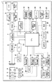
図1は、本発明の第1の実施形態における撮像装置1の構成を示すブロック図である。図1において、撮影レンズ鏡筒31は、ズームレンズ群2、フォーカスレンズ群3、更に、ズームレンズ群2及びフォーカスレンズ群3等の撮像光学系を透過した光束の量を制御するである絞り4等からなる。撮像光学系を透過し、絞り4によって光量調節された被写体像光は、撮像素子5の受光面に結像され、撮像素子5はこの結像した被写体像光を光電変換して電気的な画像信号を出力する。
<First Embodiment>
FIG. 1 is a block diagram showing the configuration of the
撮像回路6は撮像素子5から出力された画像信号を受けて各種の画像処理を施すことにより所定のフォーマットの画像信号を生成し、A/D変換回路7は撮像回路6により生成されたアナログ画像信号をデジタル画像信号(画像データ)に変換する。A/D変換回路7から出力された画像データは、バッファメモリ等のメモリ(VRAM)8に一時的に記憶される。D/A変換回路9はVRAM8に記憶された画像データを読み出してアナログ画像信号に変換すると共に、再生表示に適する形態の画像信号に変換し、液晶表示装置(LCD)等の画像表示装置(以下、「LCD」と呼ぶ。)10はこのアナログ画像信号を表示する。また、撮像素子5により周期的に得られた画像を上記手順を経て順次表示することにより、電子ビューファインダ(EVF)として用いることができる。
The imaging circuit 6 receives the image signal output from the
圧縮伸長回路11は圧縮回路と伸長回路とからなり、圧縮回路は、VRAM8に一時記憶された画像データを読み出し、記憶用メモリ12への記憶に適した形態に変換するために圧縮処理や符号化処理等を施す。また、伸長回路は、記憶用メモリ12に記憶された画像データを、再生表示等をする為に適した形態に変換するための復号化処理や伸長処理等を施す。記憶用メモリ12は半導体メモリ等からなり、画像データを記憶する。記憶用メモリ12としては、フラッシュメモリ等の半導体メモリや、カード形状やスティック形状をし、撮像装置1に対して着脱自在に形成されるカード型フラッシュメモリ等の半導体メモリが用いられる。他にも、ハードディスクやフロッピー(登録商標)ディスク等の磁気記憶媒体等、様々な形態のものが適用される。
The compression /
例えば、後述する操作スイッチ24のうち、不図示のモード切替スイッチが操作されて撮影モードになり、更にレリーズスイッチが操作されて露光記録動作が指示されると、以下の処理が行われる。まず、上述したようにしてVRAM8に一時記憶された画像データは圧縮伸長回路11の圧縮回路により圧縮及び符号化された後、記憶用メモリ12に記憶される。また、再生モードになると再生動作が開始され、以下の処理が行われる。まず、記憶用メモリ12に圧縮された形で記憶された画像データは圧縮伸長回路11の伸長回路において復号化処理や伸長処理等が施された後、VRAM8に一時的に記憶される。VRAM8に一時的に記憶された画像データはD/A変換回路9を介して上述した処理により表示に適したフォーマットのアナログ信号に変換され、LCD10に画像として再生表示される。
For example, among the
CPU15は演算用のメモリを内蔵し、撮像装置1全体の制御を行う。AE処理回路13は、A/D変換回路7から出力される画像データに基づいて自動露出(AE)処理を行う。より具体的には、AE処理回路13は、A/D変換回路7によってデジタル化された一画面分の画像データの輝度値に対して累積加算等の演算処理を行って、被写体の明るさに応じたAE評価値(測光結果)を算出する。このAE評価値はCPU15に出力される。
The
スキャンAF処理回路14は、A/D変換回路7から出力される画像データに基づいて自動焦点調節(AF)処理を行う。より具体的には、A/D変換回路7によってデジタル化された一画面分の画像データの内、AF領域として指定された画面の一部分の領域に相当する画像データの高周波成分をハイパスフィルタ(HPF)等を介して抽出する。更に、累積加算等の演算処理を行って、高域側の輪郭成分量等に対応するAF評価値(焦点評価値)を算出する。なお、AF領域は、例えば、中央部分あるいは画面上の任意の部分の一箇所である場合や、中央部分あるいは画面上の任意の部分とそれに隣接する複数箇所である場合、離散的に分布する複数箇所である場合などがある。
The scan
タイミングジェネレータ(TG)16は所定のタイミング信号を発生する。センサードライバー17は撮像素子5を駆動する。TG16は、所定のタイミング信号をCPU15、撮像回路6、センサードライバー17へ出力し、CPU15はこのタイミング信号に同期させて各種の制御を行う。また撮像回路6は、TG16からのタイミング信号を受け、これに同期させて色信号の分離等の各種画像処理を行う。さらにセンサードライバー17は、TG16のタイミング信号を受け、これに同期して撮像素子5を駆動する。
A timing generator (TG) 16 generates a predetermined timing signal. The
また、絞り駆動モータ21は絞り4を駆動し、第1モータ駆動回路18は絞り駆動モータ21を駆動制御する。フォーカス駆動モータ22はフォーカスレンズ群3を駆動し、第2モータ駆動回路19はフォーカス駆動モータ22を駆動制御する。ズーム駆動モータ23はズームレンズ群2を駆動し、第3モータ駆動回路20はズーム駆動モータ23を駆動制御する。
The
CPU15は、第1モータ駆動回路18、第2モータ駆動回路19、第3モータ駆動回路20をそれぞれ制御する。これにより、絞り駆動モータ21、フォーカス駆動モータ22、ズーム駆動モータ23を介して、絞り4、フォーカスレンズ群3、ズームレンズ群2をそれぞれ駆動制御する。CPU15はAE処理回路13において算出されたAE評価値等に基づき適正な露光量になる電荷蓄積時間及び絞り値を求め、第1モータ駆動回路18を制御して絞り駆動モータ21を駆動し、絞り4の絞り量が適正になるように調整するAE制御を行う。
The
またCPU15はスキャンAF処理回路14において算出されるAF評価値もしくは後述する位相差AF処理回路37で求められた二像の位相差に基づき第2モータ駆動回路19を制御してフォーカス駆動モータ22を駆動する。これにより、フォーカスレンズ群3を合焦位置に移動させるAF制御を行う。また操作スイッチ24のうち不図示のズームスイッチが操作された場合、CPU15は、第3モータ駆動回路20を制御してズーム駆動モータ23を駆動制御することによりズームレンズ群2を移動させ、撮像光学系の変倍動作(ズーム動作)を行う。
Further, the
操作スイッチ24は各種のスイッチ群からなり、例えば、以下のものがある。まず、撮像装置1を起動させて電源供給を行うための主電源スイッチや撮影動作(記憶動作)等を開始させるレリーズスイッチ、再生動作を開始させる再生スイッチ、ズーム倍率の変更、すなわち、ズームレンズ群2の移動を指示するズームスイッチ等である。他に、光学式ファインダー(OVF)電子ビューファインダー(EVF)切り替えスイッチ等がある。本実施の形態では、レリーズスイッチは、第1ストローク(以下、「SW1」と呼ぶ。)と、第2ストローク(以下、「SW2」と呼ぶ。)との二段スイッチにより構成される。SW1がオンになると撮像動作に先立ってAE処理及びAF処理を開始させる指示信号を発生する。また、SW2がオンになると画像を撮影して記録する露光記録動作を開始させる指示信号を発生する。
The
EEPROM25は各種制御等を行うプログラムや各種動作を行わせるために使用するデータ等が予め記憶されている電気的に書き換え可能な読み出し専用メモリである。26は電池、28はフラッシュ発光部、27はフラッシュ発光部28の閃光発光を制御するスイッチング回路、29は警告表示などを行うLEDなどの表示素子、30は音声によるガイダンスや警告などを行うためのスピーカーである。
The
AF補助光発光部33はAF評価値を取得する際に被写体の全部または一部を照明するLEDなどの光源で構成され、AF補助光駆動回路32はAF補助光発光部33を駆動する。
The AF auxiliary
振れ検出センサー35は手振れなどを検出し、振れ検出回路34は振れ検出センサー35の信号を処理する。顔検出回路36はA/D変換回路7からの出力を受けて画面上での顔位置や顔の大きさなどを検出する。顔検出回路36においては、A/D変換回路7から出力される画像データから、目、眉などの顔を特徴付ける部分を画像上で探索し、人物の顔の画像上での位置を求める。更に顔の大きさや傾きなどを、顔を特徴付ける部分の間隔などの位置関係から求める。
The shake detection sensor 35 detects camera shake and the like, and the
位相差AF処理回路37は、位相差方式による焦点検出処理(位相差AF)用の信号の像修正を行った後、基準画像(A像)と参照画像(B像)の相関演算を行い、二像の信号が一致する像ずれ量(二像の位相差)を計算する。本実施形態では、撮像面に、位相差AFを行うための画素を配置している。
The phase difference
そしてCPU15において、位相差AF処理回路37で求められた二像の位相差からデフォーカス量及び合焦させるためのフォーカスレンズ群3の駆動量を求めることで位相差AFが行われる。
Then, the
次に撮像素子5に含まれる画素の構成について図2及び図3を参照して説明する。図2は、画素の構成の一例を示す回路図である。画素部201はフォトダイオード202、転送トランジスタ203、信号増幅アンプ204、リセット用トランジスタ205を1単位(画素)として構成されている。転送トランジスタ203及び、リセット用トランジスタ205は、垂直走査回路206からの信号によって動作する。垂直走査回路206にはシフトレジスタや、転送トランジスタ203等の各画素を駆動させる信号生成回路等が含まれる。そして、生成されたタイミング信号(TX1〜4、RS1〜4等)により転送トランジスタ203及びリセット用トランジスタ205を制御することによって、フォトダイオード202の電荷をリセットしたり、読み出したりして電荷蓄積時間を制御する。図2では4画素分のみを表しているが、実際には画素部201と同様の画素を単位として、多数の画素が二次元的に配置されている。
Next, the configuration of the pixels included in the
本実施形態では、このように二次元的に配置される画素は、通常の撮像用画素と位相差AF用の画素(焦点検出用画素)を含む。撮像面で位相差AFを行うために、図3(a)に示すように、位相差AF用画素はAL1層において、開口を通常の撮像用画素に比べて制限し、マイクロレンズを通して見る射出瞳を偏らせるようにしている。これにより、位相差AF用画素は、撮影レンズ鏡筒31に含まれるレンズの異なる射出瞳領域を通過した一対の光を受光することになる。図3(b)は、撮像素子5の受光面における開口に対応する受光領域(開口を介して光が入射する領域)の一例を示す図である。基準画像(A像)と参照画像(B像)を得るために、それぞれ反対方向に開口が配置されている。位相差AF用画素の開口率は、撮像用画素の開口率の4分の1程度まで低下する場合があり、LCD10に表示する画像の輝度が適正(予め決められた範囲)になるような露光条件にした場合には、位相差AF用画素の露光量は大幅に不足することになる。
In the present embodiment, the pixels arranged two-dimensionally in this manner include normal imaging pixels and phase difference AF pixels (focus detection pixels). In order to perform the phase difference AF on the imaging surface, as shown in FIG. 3A, the phase difference AF pixel has an aperture limited in the AL1 layer as compared with a normal imaging pixel, and the exit pupil viewed through the microlens. Is biased. As a result, the phase difference AF pixel receives a pair of lights that have passed through different exit pupil regions of the lenses included in the
209は水平走査回路であり、シフトレジスタ(不図示)、列アンプ回路210、信号出力選択スイッチ211及び外部への出力回路(不図示)等が含まれる。列アンプ回路210の設定を、センサードライバー17からの信号によって変化させることによって、画素から読み出された信号を増幅することができる。
A
位相差AF用画素と撮影用画素は例えば、図4のように配置されている。図4において「A」と記載された画素は位相差AF用画素のうち基準画像を形成する画素、「B」と記載された画素は位相差AF用画素のうち参照画像を形成する画素、その他の画素は撮像用画素である。 For example, the phase difference AF pixel and the imaging pixel are arranged as shown in FIG. In FIG. 4, a pixel described as “A” is a pixel that forms a reference image among the pixels for phase difference AF, a pixel that is described as “B” is a pixel that forms a reference image among pixels for phase difference AF, and the like These pixels are imaging pixels.
次に、上記構成を有する撮像装置1を用いて通常の撮影を行う際の動作について説明する。図5は、第1の実施形態における通常画像を取得する際に、垂直走査回路206から生成される信号を示したタイミングチャートである。
Next, an operation when performing normal shooting using the
まず、TX1信号及びRS1信号が共に立ち上がることによって、転送トランジスタ203及びリセット用トランジスタ205が導通し、フォトダイオード202の電荷がリセットされる。リセット後、TX1信号がローになると電荷蓄積が開始される。その後所定時間の経過後に、TX1信号が再度立ち上がり、フォトダイオード202に蓄積された電荷を転送トランジスタ203を介して信号増幅アンプ204に読み出す。TX1信号がローになってから、TX1信号が立ち上がるまでの時間が電荷蓄積時間(シャッタースピード)となる。この動作は、TG16によって設定された条件で、所定の順番(図5に示す例では、TX1からTX4、RS1からRS4の順番)で順次行われる。そして、信号増幅アンプ204からの信号から画像信号を生成し、水平走査回路209を通して出力される。この動作も、TG16によって設定された条件で行われる。
First, when both the TX1 signal and the RS1 signal rise, the
本実施形態において、撮像装置1に搭載されている撮像素子5はCMOS型の撮像素子である。そのため、垂直走査回路206のシフトレジスタの設定によって、どの行の転送トランジスタ203をどのような順序で駆動させるかを選択することができ、また、同一行を繰り返し選択して信号を読み出すこともできる。また、水平走査回路209のシフトレジスタの設定によって、どの列の選択スイッチ211を動作させるかによって、読み出された行の信号の内、どの列の信号から出力するかを選択することができる。これによって、画面内のどの画素からどのような順番で読みだすかを指定することができる。
In the present embodiment, the
図6は、電荷蓄積時間と、蓄積された電荷が画像として読み出されるタイミングを示す。TG16及びセンサードライバー17が生成する垂直同期信号によって、露光及び信号読み出しが行われる。
FIG. 6 shows the charge accumulation time and the timing at which the accumulated charge is read out as an image. Exposure and signal readout are performed by a vertical synchronization signal generated by the
次に、上記構成を有する撮像装置1における本第1の実施形態における撮影動作について、図7〜図12を参照して説明する。図7は、撮影動作のメインフローを示すフローチャートであり、撮像装置1の主電源スイッチがオン状態であり、かつ撮像装置1の動作モードが撮影(録画)モードにあるときに、撮像素子5等への電源供給などを行って撮影を可能にして、撮影動作が行われる。
Next, the photographing operation in the first embodiment in the
まずS1においてCPU15は、LCD10に表示するEVF表示と、位相差AFとを並行して行うための撮像素子5の駆動モードの設定を行う。この駆動モードのタイミングチャートを図8に示す。この駆動モードでは、EVF用の画像信号も位相差AF用の画像信号も、撮像素子5からの読み出しレートは最大で60fps程度になるよう設定される。
First, in S <b> 1, the
上述したように、位相差AF用画素の開口率は撮像用画素より低い。そのため、本第1の実施形態では位相差AF用画素と撮像用画素とを異なる露光条件で露光し、位相差AF用画素からの画像信号と撮像用画素からの画像信号とをほぼ同時に読み出すようにする。より具体的には、図8に示すように、EVF用の画像信号を得るための電荷蓄積時間よりも、位相差AF用の画像信号を得るための電荷蓄積時間を長くする。これに伴い、位相差AF動作を行うための信号の読み出しレートが遅くなる。そのために、EVF用の画像信号と位相差AF用の画像信号のそれぞれを得るために露出条件を2行毎に設定し、撮像素子5のリセット、出力転送のタイミングを異ならせる。実際の露光条件の設定は、S2のAE処理において設定される。
As described above, the aperture ratio of the phase difference AF pixel is lower than that of the imaging pixel. Therefore, in the first embodiment, the phase difference AF pixel and the imaging pixel are exposed under different exposure conditions so that the image signal from the phase difference AF pixel and the image signal from the imaging pixel are read out almost simultaneously. To. More specifically, as shown in FIG. 8, the charge accumulation time for obtaining the image signal for phase difference AF is made longer than the charge accumulation time for obtaining the image signal for EVF. Along with this, the signal reading rate for performing the phase difference AF operation becomes slow. For this purpose, exposure conditions are set for every two rows in order to obtain each of the EVF image signal and the phase difference AF image signal, and the reset timing of the
EVF画像用の露光条件は、撮影者による被写体の視認に適した最適な露光量、パンニングや被写体の移動に対する追従性等を考慮して決める必要がある。一方、位相差AF用の画像信号の露光条件は、位相差AFに最適な露光量、AF時間、AF時間内の被写体の移動及び手振れによるAFへの影響等を考慮して、特に電荷蓄積時間を決める。図3に示したように撮像用画素と位相差AF用画素とでは開口率が異なると共に、撮像素子5の中心から離れた位置では撮影レンズ鏡筒31の射出瞳から入射する光束が斜めになるために入射光量が減少する。よって、位相差AF用画素は撮像用画素に比べて開口率の比以上(例えば4倍程度以上)の露光量を必要とする。
The exposure condition for the EVF image needs to be determined in consideration of the optimal exposure amount suitable for the photographer's visual recognition of the subject, panning, followability to the movement of the subject, and the like. On the other hand, the exposure conditions of the image signal for phase difference AF are particularly determined in consideration of the exposure amount optimal for phase difference AF, the AF time, the movement of the subject within the AF time, the influence on AF due to camera shake, and the like. Decide. As shown in FIG. 3, the aperture ratio differs between the imaging pixel and the phase difference AF pixel, and the light beam incident from the exit pupil of the
ここで、S2で行われる本第1の実施形態におけるAE処理の詳細について図9を用いて説明する。まずS21において、撮影して得られた画像データに基づいてAE処理回路13において算出されるAE評価値を参照し、EVF画像用の露光条件として、絞り、増幅率及び電荷蓄積時間を組み合わせて適正な露光量になるように決定する。この際、EVF画像用の電荷蓄積時間は、8分の1秒を長秒時側の限度、撮像素子5の性能等で決まる最短電荷蓄積時間を短秒時側の限度とする。増幅率は列アンプ回路210の値を調整して設定する。各値の決め方はプログラム線図と呼ばれる、被写体輝度が測定された場合に、絞り、増幅率及び電荷蓄積時間を一律に決める手法を用いて行われている。その詳細は例えば、特開2000−78461、特開平4−70632等に記載されており公知であるため、ここでの説明は割愛する。
Here, details of the AE process in the first embodiment performed in S2 will be described with reference to FIG. First, in S21, referring to the AE evaluation value calculated in the
次いでS22において、設定された露光条件を用いて得られた画像データに基づいて、再度AE処理回路13によりAE評価値を算出し、算出したAE評価値に基づいてS23において適正な露光条件を再度決定する。そしてS24で再度決定された露光条件と、前回設定された露光条件との差が予め決められた範囲内であるかどうかを判定する。予め決められた範囲内でない場合はS22に戻って、予め決められた範囲内となるまで、露光条件を決定する処理を繰り返す。
Next, in S22, an AE evaluation value is calculated again by the
露光条件の差が予め決められた範囲内であれば(S24でYES)、S25以降で行われる位相差AF用の露光条件を決定する処理に移る。ただし、位相差AF用の露光条件における絞りはEVF用の露光条件における絞りと同じなので、電荷蓄積時間と増幅率を決定していく。 If the difference in exposure conditions is within a predetermined range (YES in S24), the process proceeds to processing for determining the exposure conditions for phase difference AF performed in S25 and thereafter. However, since the diaphragm in the exposure condition for phase difference AF is the same as the diaphragm in the exposure condition for EVF, the charge accumulation time and the amplification factor are determined.
まずS25において、位相差AF用の電荷蓄積時間及び増幅率を求める。AE処理回路13において求められるAE評価値は開口率の高い撮像用画素から出力される画像信号、すなわちEVF用の画像データを基に行われる。よってEVF画像に最適な電荷蓄積時間が求められたならば、その値を、開口率の比率に、中心画素に対する像高による入射光量の減光量の比を掛けた値の逆数倍すれば良い。例えば開口率が3分の1、減光量が0.8倍なら露光量は3.75倍とし、開口率が4分の1、減光量が0.8倍なら露光量は5倍とすれば良い。
First, in S25, the charge accumulation time and amplification factor for phase difference AF are obtained. The AE evaluation value obtained in the
この減光量は入射光束の像高による入射角度に依存するため、撮影レンズ鏡筒31の射出瞳距離と像高及び位相差AFを行う際の絞り値の関数となる。よって画面全体で位相差AFを行う場合はその平均値を用いるが、撮影者により焦点検出を行うための画面上の位置(AF点)の選択が行われた場合など、位相差AFを行う領域(焦点検出領域)が画面上の一部に限定される場合は、その領域の減光量を計算する。
Since this light reduction amount depends on the incident angle depending on the image height of the incident light beam, it becomes a function of the exit pupil distance of the photographing
そして、上述したように、開口率の割合と計算した減光量とに基づいて、電荷蓄積時間の変更と増幅率の設定を行う。電荷蓄積時間は位相差AFに要する時間が必要以上に長くならないように、EVF画像表示の更新時間(周期)を長秒時側の限度とする。また撮像素子5の性能等で決まる最短電荷蓄積時間を短秒時側の限度とする。更に手振れによるAF精度の劣化を考える必要があるので、焦点距離が所定値より長い場合は、上限値を焦点距離に応じて小さくする。
As described above, the charge accumulation time is changed and the amplification factor is set based on the ratio of the aperture ratio and the calculated light reduction amount. The charge accumulation time has an EVF image display update time (cycle) as a limit on the long second side so that the time required for the phase difference AF does not become longer than necessary. In addition, the shortest charge accumulation time determined by the performance of the
EVF画像に最適な電荷蓄積時間を逆数倍して決めた電荷蓄積時間が上限値より長くなった場合は、EVF画像表示の更新時間を電荷蓄積時間とし、不足する露光量は信号を増幅することで補う。例えば、EVF画像表示の更新時間が8分の1秒、計算された電荷蓄積時間が4分の1秒となった場合は、電荷蓄積時間を8分の1秒として、2倍の信号増幅を行う。上述したように、増幅率は列アンプ回路210の値を調整して設定する。但し、信号のSN比の観点から増幅率の設定にも上限があるので、EVF画像表示の更新時間を電荷蓄積時間とし増幅率を上限に設定してもなお露光量が不足する場合は、上記の上限値より長くなっても構わないので、電荷蓄積時間を延ばして対応する。
When the charge accumulation time determined by reciprocally multiplying the optimum charge accumulation time for the EVF image becomes longer than the upper limit, the EVF image display update time is set as the charge accumulation time, and the insufficient exposure amount amplifies the signal. Make up for it. For example, if the EVF image display update time is 1/8 second and the calculated charge accumulation time is 1/4 second, the charge accumulation time is 1/8 second and the signal amplification is doubled. Do. As described above, the amplification factor is set by adjusting the value of the
次いでS26において、S25で求めた露光条件で撮影をした場合に、位相差AF用画素に飽和画素が生じるかを調べる。飽和は位相差AFに悪影響を及ぼすため、位相差AF用の画素が飽和しないように露光条件を微調整していく必要がある。飽和する画素が生じない場合は、S23で求めた露光条件をEVF用の露光条件とし、S25で求めた電荷蓄積時間及び増幅率、そしてS23で求めた絞りを位相差AF用の露光条件として、図7の処理に戻る。 Next, in S26, it is checked whether or not a saturated pixel is generated in the phase difference AF pixel when photographing is performed under the exposure condition obtained in S25. Since saturation adversely affects the phase difference AF, it is necessary to finely adjust the exposure conditions so that the pixels for the phase difference AF are not saturated. When the saturated pixel does not occur, the exposure condition obtained in S23 is used as the EVF exposure condition, the charge accumulation time and amplification factor obtained in S25, and the aperture obtained in S23 is used as the exposure condition for phase difference AF. Returning to the process of FIG.
飽和する画素が生じるか否かは、AE評価値を得た時点で位相差AF用画素からの出力信号と開口率の比率から判定することができる。まず、AE評価値を得た時点で位相差AF用画素の出力信号の最大値を調べ、その値を上述したように逆数倍する。逆数倍した値が飽和値を超えるようであれば、これまでの手順で決めた露光条件では位相差AF用画素の出力信号に飽和が生じると予測できる。これは、EVF用の露光条件にてAE評価値を算出し、その値を上述したように逆数倍して位相差AF用の露光条件としているからである。飽和画素が生じる場合は、S27において、電荷蓄積時間及び増幅率の調整を行う。まず、
係数1=(飽和値)÷(EVF用の露光条件での位相差AF用の画像信号の最大値)
により求められた係数1を、S23で求められたEVF用の電荷蓄積時間に掛けたものを、位相差AF用の電荷蓄積時間とする。もし求めた電荷蓄積時間が上限値より長くなった場合は、EVF画像表示の更新時間を電荷蓄積時間とし、不足する露光量は信号を増幅することで補う。例えば、EVF画像表示の更新時間が8分の1秒、計算された電荷蓄積時間が4分の1秒となった場合は、電荷蓄積時間を8分の1秒として、2倍の信号増幅を行う。増幅率は列アンプ回路210の値を調整して設定する。但し、信号のSN比の観点から増幅率の設定にも上限があるので、EVF画像表示の更新時間を電荷蓄積時間とし増幅率を上限に設定してもなお露光量が不足する場合は、上記の上限値より長くなっても構わないので、電荷蓄積時間を延ばして対応する。
Whether or not a saturated pixel occurs can be determined from the ratio between the output signal from the phase difference AF pixel and the aperture ratio when the AE evaluation value is obtained. First, when the AE evaluation value is obtained, the maximum value of the output signal of the phase difference AF pixel is checked, and the value is reciprocally multiplied as described above. If the reciprocal value exceeds the saturation value, it can be predicted that saturation will occur in the output signal of the phase difference AF pixel under the exposure conditions determined in the procedure so far. This is because the AE evaluation value is calculated under EVF exposure conditions, and the value is reciprocally multiplied as described above to obtain the exposure conditions for phase difference AF. If a saturated pixel occurs, the charge accumulation time and the amplification factor are adjusted in S27. First,
The value obtained by multiplying the
なお、上述した様にして位相差AF用の電荷蓄積時間を決めるのは通常被写体の場合であり、イルミネーション、天体、夕日、朝日などの点光源と称される被写体に対してAFを行う場合は、逆数倍して電荷蓄積時間を求める必要はない。これらの被写体では飽和が起きるので、公知の方法(例えば、特開2011−150281等に記載された方法)で点光源被写体が存在すると判定された場合は、EVF用の画像の露光条件と同じ露光条件とする。この露光条件で飽和画素があるかを調べ、飽和画素がある場合はS27において、電荷蓄積時間及び増幅率の調整を行う。その後、図7のS3に進み、S27で調整した電荷蓄積時間及び増幅率、そしてS23で求めた絞りを位相差AF用の露光条件とする。 Note that the charge accumulation time for phase difference AF is determined in the case of a normal subject as described above, and when AF is performed on a subject called a point light source such as illumination, celestial object, sunset, and sunrise. It is not necessary to obtain the charge accumulation time by reciprocal multiplication. Since saturation occurs in these subjects, if it is determined that a point light source subject is present by a known method (for example, a method described in Japanese Patent Application Laid-Open No. 2011-150281), the same exposure as the EVF image exposure condition is performed. Condition. It is checked whether there is a saturated pixel under this exposure condition. If there is a saturated pixel, the charge accumulation time and amplification factor are adjusted in S27. Thereafter, the process proceeds to S3 in FIG. 7, and the charge accumulation time and amplification factor adjusted in S27, and the diaphragm obtained in S23 are set as exposure conditions for phase difference AF.
露光条件が決まったならば、S3において、決定した露光条件で撮影を行い、撮像用画素に結像した像をLCD10に画像として表示する。ここでは、TX信号及びRS信号を図8のように制御する。図8はEVF用の画像信号及び位相差AF用の画像信号を得るための垂直走査回路206から生成される信号を示したタイミングチャートである。
If the exposure conditions are determined, shooting is performed under the determined exposure conditions in S3, and an image formed on the imaging pixels is displayed on the
図8に示すタイミングチャートに示すタイミングで撮像素子5を駆動することで、EVF用の画像信号と位相差AF用の画像信号とを異なる露光条件、且つ異なる読み出しレートで、ほぼ同時に得ることができる。そのために、EVF用の画像と位相差AF用の信号のそれぞれの露出条件を2行毎に設定し、撮像素子5のリセット及び出力転送のタイミングを異ならせる。
By driving the
すなわちEVF用の信号及び位相差AF用の信号は、TX信号及びRS信号が立ち上がることによって、各画素のフォトダイオード202の電荷がリセットされ露光が開始される。この動作はTG16によって設定された条件で、画素部201から所定の順番で順次行われる。その後、EVF用の画像を取得するための行において、S2で決められたEVF用の電荷蓄積時間の経過後に、TX1及びTX2信号が順次立ち上がり、フォトダイオード202の電荷を信号増幅アンプ204に読み出す。読み出した信号は、水平走査回路209を通して出力され、EVF用の画像信号を取得する。
That is, for the EVF signal and the phase difference AF signal, when the TX signal and the RS signal rise, the charge of the
その後、再度TX1,RS1信号及びTX2,RS2信号が順次立ち上がり、EVF用の行をリセットする。EVF用の画像信号を取得するためこの動作を繰り返す。なお、図8に示す例では、1垂直同期期間に、EVF用の画像信号を3回、位相差AF用の画像信号を1回、読み出している。この場合、3回読み出したEVF用の画像信号の内、2回分のEVF用の画像信号を読み捨てる。EVF用の画像信号と位相差AF用の画像信号をほぼ同時に得るためには、最後に読み出したEVF用の画像信号をLCD10へのEVF表示に用いれば良い。また、1垂直同期期間にEVF用の画像信号を1回のみ読み出すように、TX1、TX2、RS1、RS2信号のタイミングを制御してもよい。このようにして得られた画像信号に基づくEVF画像は、LCD10に表示される。
After that, the TX1, RS1 and TX2, RS2 signals sequentially rise again to reset the EVF row. This operation is repeated in order to acquire an image signal for EVF. In the example shown in FIG. 8, the EVF image signal is read out three times and the phase difference AF image signal is read out once in one vertical synchronization period. In this case, among the EVF image signals read out three times, two EVF image signals are read out and discarded. In order to obtain the image signal for EVF and the image signal for phase difference AF almost simultaneously, the image signal for EVF read last may be used for EVF display on the
同様に、位相差AF用の画像信号を取得するために、S2で決められた位相差AF用の電荷蓄積時間の経過後に、TX3及びTX4信号が順次立ち上がり、フォトダイオード202の電荷を信号増幅アンプ204に読み出す。読み出した画像信号は、水平走査回路209を通して出力され、位相差AF用の画像信号を取得する。
Similarly, in order to obtain an image signal for phase difference AF, after the charge accumulation time for phase difference AF determined in S2, the TX3 and TX4 signals sequentially rise and the charge of the
次いでS4において、レリーズスイッチの状態を確認する。撮影者によってレリーズスイッチが操作され、SW1がオン状態になったことをCPU15が確認すると、次のS5に進み、位相差AF処理を行う。この処理については後述する。
Next, in S4, the state of the release switch is confirmed. When the release switch is operated by the photographer and the
位相差AF処理の結果、S6で合焦可能と判断されればS9に進み、AFOK表示を行う。ここでは例えば、LED29を点灯したり、LCD10上に例えば緑の枠を表示するなどの処理を行う。一方、S6において、合焦可能と判断されなかった場合には、S7に進んで撮像素子5の駆動タイミングを図11に示すように変更する。なお、絞りは変更しない。
If it is determined in S6 that focusing is possible as a result of the phase difference AF process, the process proceeds to S9, and AFOK display is performed. Here, for example, processing such as turning on the
S7では、後述するS8で行うスキャンAF処理の高速化のため、スキャンAF用の画素信号を得るためのフレームレートを速く設定する。フレームレートを速く設定すると電荷蓄積時間が短くなるため、その分増幅率を大きくして信号のレベルを確保する。しかしながら、増幅率が大きすぎると良好なスキャンAF結果が期待できないので、増幅率の上限を定めておき、それを超える場合は上限の増幅率とし、電荷蓄積時間を調整して適正な露光量を確保する。この場合でも図8に示す駆動タイミングに比べて、電荷蓄積時間は短くなる。 In S7, the frame rate for obtaining the pixel signal for scan AF is set fast in order to speed up the scan AF process performed in S8 described later. If the frame rate is set fast, the charge accumulation time is shortened, so the amplification level is increased correspondingly to ensure the signal level. However, since a good scan AF result cannot be expected if the amplification factor is too large, an upper limit is set for the amplification factor, and if it exceeds that, the upper limit amplification factor is set, and an appropriate exposure amount is adjusted by adjusting the charge accumulation time. Secure. Even in this case, the charge accumulation time is shorter than the drive timing shown in FIG.
例えば、増幅率の上限が5段、EVF画像に最適な電荷蓄積時間が30分の1秒、増幅率が0であれば、増幅率を2段とすると、スキャンAF用の電荷蓄積時間は120分の1秒となる。しかし、低照度になりEVF用画像に最適な電荷蓄積時間が30分の1秒、増幅率が4段の場合、増幅率を上限の5段とすると、スキャンAF用の電荷蓄積時間は60分の1秒となる。なお、スキャンAF処理中は、EVF用の画素をスキャンAF用の画素として用いる。 For example, if the upper limit of the amplification factor is five, the charge accumulation time optimal for EVF images is 1/30 second, and the amplification factor is 0, the charge accumulation time for scan AF is 120 when the amplification factor is two. One second of a minute. However, if the charge accumulation time is 1/30 second optimal for an EVF image due to low illuminance and the amplification factor is four stages, the charge accumulation time for scan AF is 60 minutes if the amplification factor is the upper limit of five stages. 1 second. Note that during the scan AF process, the EVF pixels are used as the scan AF pixels.
S8においてスキャンAF処理を行う。なお、スキャンAFの処理については、図11及び図12を参照して詳細に後述する。また、スキャンAF処理の最後に撮像素子5の駆動タイミングを図8に示す駆動タイミングに戻す。スキャンAF処理の結果、合焦可能と判断されれば、S9に進みAFOK表示を行う。
In S8, scan AF processing is performed. The scan AF process will be described later in detail with reference to FIGS. At the end of the scan AF process, the drive timing of the
またS8において、合焦可能と判断されなかった場合には、S9に進みAFNG表示を行う。これはLED29を点滅表示することなどにより行うと同時にLCD上に黄色の枠を表示するなどの処理を行う。
If it is not determined in S8 that focusing is possible, the process proceeds to S9 and AFNG display is performed. This is performed by, for example, blinking the
CPU15はS10においてSW2の確認を行い、SW2がオンになっていたならばS11に進み、撮影を行い、撮影が終了すると一連の撮像動作を終了する。
The
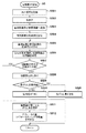
次に、S5で行う合焦位置を検出するための位相差AF処理の概略について、図10を用いて説明する。上述したように、EVF用の画像信号と位相差AF用の画像信号は異なる露光条件で取得するように、EVF用と位相差AF用それぞれの露出条件を2行毎に設定する。これにより、位相差AF処理中もEVF用の画像信号を取得できるので、取得したEVF用の画像信号の画像をLCD10に表示する。
Next, an outline of the phase difference AF process for detecting the focus position performed in S5 will be described with reference to FIG. As described above, the exposure conditions for EVF and phase difference AF are set every two rows so that the EVF image signal and the phase difference AF image signal are acquired under different exposure conditions. Thus, since the EVF image signal can be acquired even during the phase difference AF process, the acquired image of the EVF image signal is displayed on the
まずS501において、A/D変換回路7より出力される位相差AF用の画像信号を位相差AF処理回路37の所定の記録領域に記録する。次いでS502において、記録された像の修正を行う。上述したように本実施形態では、撮像面に位相差AFを行う画素を配置している。そのため、外部位相差AFのように、像高による光束の違いにより生じる像の歪みを修正するフィールドレンズや、位相差AF用センサーへ入射する光束の瞳位置を制限するための絞り、不要な光束を遮断するためのマスクを結像面とセンサーの間に配置できない。そのため、位相差AF用の信号は画素毎にシェーディング・オフセットが異なるため、その補正が必要である。よって位相差AF処理回路37は像修正機能と、相関演算を行いデフォーカス量を求める機能を担っている。
First, in S 501, the phase difference AF image signal output from the A /
このシェーディングは光軸中心からの画素の位置(像高)、撮影レンズの射出瞳位置、絞り、画素内の開口部の位置によって異なるため、それぞれの要因に関して像修正量を持ち、要因に応じて位相差AF用の画素毎に像修正を行っていく。また、オフセットは位相差AF用画素の増幅率及び画素内の開口部の位置、更に位相差AF用画素の列アンプの特性によって異なるため、それぞれの要因に関して像修正量を持ち、要因に応じて位相差AF用画素毎に像修正を行っていく。なお、像修正方法の詳細に関しては、例えば、特開2012−252280等で公知なので、説明は割愛する。 This shading varies depending on the pixel position (image height) from the center of the optical axis, the exit pupil position of the taking lens, the aperture, and the position of the aperture in the pixel. Image correction is performed for each pixel for phase difference AF. In addition, since the offset differs depending on the amplification factor of the phase difference AF pixel, the position of the opening in the pixel, and the characteristics of the column amplifier of the phase difference AF pixel, each factor has an image correction amount. Image correction is performed for each pixel for phase difference AF. The details of the image correction method are well known in, for example, Japanese Patent Application Laid-Open No. 2012-252280, and will not be described.
そして、S503において、像修正された位相差AF用の画像信号の並び替えを行い、基準画像と参照画像を生成する。位相差AF用画素は例えば、図4のように配置されている。 In step S503, the image signals for phase difference AF whose images have been corrected are rearranged to generate a standard image and a reference image. For example, the phase difference AF pixels are arranged as shown in FIG.
位相差AF処理回路37に記録されているのは、図に示す「A」と「B」の位相差AF用の画素の出力であり、読み出しの順序は「A」→「B」→「A」→「B」→…→「A」→「B」となっている。S502での像修正後も同じ順序で位相差AF処理回路37の所定の記録領域に記録されている。そこで「A」と記載された基準画像を構成する画素から出力された画像信号だけを抽出して、抽出した順序に並べ基準画像(A像)とする。同様に「B」と記載された参照画像を構成する画素から出力された画像信号だけを抽出して、抽出した順序に並べ参照画像(B像)とする。
What is recorded in the phase difference
その後S504において相関演算を行う際の初期値を設定する。そして、S505において、初期値を設定された位相差AF処理回路37は式(1)に従い相関演算を行い、基準画像(A像)と参照画像(B像)との相関値を求める。
Uk=Σmax(aj+1,bj+k)-Σmax(aj,bj+k+1) …(1)
ここで、max(X,Y)はX,Yのうち大きい方をとるという意味である。またkは相関演算を行う像ずらし量、jは相関演算を行う画素数であり、S504で初期化されている。
Thereafter, in S504, an initial value for performing the correlation calculation is set. In step S <b> 505, the phase difference
Uk = Σmax (aj + 1, bj + k) −Σmax (aj, bj + k + 1) (1)
Here, max (X, Y) means the larger of X and Y. Further, k is an image shift amount for performing the correlation calculation, and j is the number of pixels for performing the correlation calculation, and is initialized in S504.
そして、S506において、CPU15は基準画像(A像)と参照画像(B像)の相関値を位相差AF処理回路37から取得する。そして、S507において既に一時記録されている相関値があれば、その相関値と符号が等しいか調べ、符号が反転した場合、また、取得された相関量が零である場合は、S507からS511へ進む。
In step S <b> 506, the
一方、符号が等しい場合にはS508において取得した相関値を一時記録されていた相関値と差し替える。一時記録された相関値が無い場合は、取得した相関値を一時記録する。そして、S509において、ずらし量が相関値を求める演算の終端の値になったか否かを調べる。終端の値になっていなければS520へ進み、ずらし量kをk←k+1と更新してS505に戻る。終端の値になっていたならばS510へ進み、位相差AFがNGと判定し、処理を終了する。 On the other hand, if the signs are equal, the correlation value acquired in S508 is replaced with the temporarily recorded correlation value. If there is no temporarily recorded correlation value, the acquired correlation value is temporarily recorded. In step S509, it is checked whether the shift amount has reached the end value of the calculation for obtaining the correlation value. If it is not the end value, the process proceeds to S520, the shift amount k is updated as k ← k + 1, and the process returns to S505. If the end value has been reached, the process proceeds to S510, the phase difference AF is determined to be NG, and the process ends.
S511では、相関量が零になるずらし量を演算する。相関値の演算は1画素づつずらして行われているため、位相差AF処理回路37において演算された相関量が零になることは稀である。そこで符号が異なる2つの相関量と、その相関量を与えるずらし量とから、相関量が零となるずらし量を求める。
In step S511, a shift amount at which the correlation amount becomes zero is calculated. Since the correlation value is calculated by shifting one pixel at a time, the correlation amount calculated in the phase difference
式(1)で相関量を計算した結果、K=lとK=l+1の間で相関量Ukの符号が反転したとすると、直線補間により相関量が零となる像ずらし量δは
δ=l+|Ul|÷[|Ul|+|Ul+1|] …(2)
となる。但し、|z|はzの絶対値を意味する。
Result of calculating the amount of correlation in Equation (1), K = the sign of the correlation quantity Uk between l and K = l + 1 is the inverted, amount to shifted image volume correlation is zero by linear interpolation δ is δ = l + | Ul | ÷ [| Ul | + | Ul + 1 |] (2)
It becomes. However, | z | means the absolute value of z.
次いでS511において、像ずれ量δから、プレディクション量Pを
P=δ―Δ …(3)
により求める。但し、Δは合焦時の像ずれ量である。そして、S512において撮影レンズ鏡筒31の特性から決まる基線長を用いることで、プレディクション量Pからデフォーカス量d(フォーカスレンズ群の移動量と方向)を
d=K・P …(4)
により求め、処理を終了する。但し、Kはフォーカスに関する敏感度で、撮影レンズ鏡筒31の焦点距離、絞り4の値、像高に依存する値なので、EEPROM25内にこれらをパラメータとするテーブルを用意しておき、そのテーブルを参照して値を求めている。S512でデフォーカス量を求めると、図7の処理に戻る。
Next, in S511, from the image shift amount δ, the prediction amount P is changed to P = δ−Δ (3)
Ask for. However, Δ is an image shift amount at the time of focusing. Then, by using the base line length determined from the characteristics of the photographing
To finish the process. However, K is a sensitivity related to the focus, and is a value depending on the focal length of the photographing
次に、図7のS8で合焦位置を検出するためのスキャンAF処理について、図11及び図12を用いて説明する。 Next, the scan AF process for detecting the focus position in S8 of FIG. 7 will be described with reference to FIGS.
なお以降の説明においては、フォーカスレンズ群3を駆動しながらAF評価値を取得する動作をスキャン、AF評価値を取得するフォーカスレンズ群3の位置をスキャン位置、スキャン位置の間隔をスキャン間隔と呼ぶ。また、AF評価値を取得する範囲(すなわち、フォーカスレンズ群3を駆動する範囲)をスキャン範囲と呼ぶものとする。
In the following description, the operation for acquiring the AF evaluation value while driving the
S8において定められた露光条件でスキャンAFを行った結果、焦点調整が可能な場合は合焦位置へフォーカスレンズ群3を制御する。逆に焦点調整が不可能な場合は、過焦点位置と呼ばれる、無限遠を被写界深度の遠側に含む、被写界深度の最も近距離のフォーカスレンズ位置へフォーカスレンズ群3を制御する。
If the focus adjustment is possible as a result of performing the scan AF under the exposure conditions determined in S8, the
スキャンAF処理中は、図11に示すタイミングチャートに示すタイミングで撮像素子5を駆動し、EVF用の画像信号の代わりに、スキャンAF用の画像信号を取得する。また、位相差AF用の画像信号は、S5の位相差AF処理時と同じ露光条件で取得し、異なる読み出しレートで、スキャンAF用の画像信号と並行して得られるようにする。そのために、スキャンAF用の画像信号と位相差AF用の画像信号のそれぞれを得るための露出条件を2行毎に設定し、撮像素子5のリセット、出力転送のタイミングを異ならせる。但し、スキャンAF処理においては位相差AF用の画像信号は使用しない。
During the scan AF process, the
スキャンAF用の電荷蓄積時間は、32分の1秒を長秒時側の限度、撮像素子5の性能等で決まる最短電荷蓄積時間を短秒時側の限度とし、絞り、列アンプ回路210の値を調整して、S3のAE処理結果を参照し、露光量が適正となるように決める。EVF表示に関してはスキャンAF中は適正にならない可能性があるが、スキャンAF用の画像信号を加算及び増幅した信号を用いることによりEVF表示に適した画像を作成するができる。なお、本処理においては、EVF表示が適正にならないとしても、スキャンAF性能を優先することとする。
The charge accumulation time for scan AF is set to 1/32 seconds on the long second time limit, and the shortest charge accumulation time determined by the performance of the
スキャンAF用の電荷蓄積時間が位相差AF用の電荷蓄積時間より短くなると、それに伴いスキャンAF用の読み出しレートが速くなる。一例として、スキャンAF用の電荷蓄積時間は128分の1秒、読み出しレートは128FPS、位相差AF用の画像の電荷蓄積時間は8分の1秒、読み出しレートは8FPSとなる。絞り4の値は変更せずそのままとする。
When the charge accumulation time for scan AF becomes shorter than the charge accumulation time for phase difference AF, the scan AF read rate increases accordingly. As an example, the charge accumulation time for scan AF is 1/128 second, the readout rate is 128 FPS, the charge accumulation time for an image for phase difference AF is 1/8 second, and the readout rate is 8 FPS. The value of the
露光条件(電荷蓄積時間)が決まったならば、TX信号及びRS信号を図11に示すように制御する。すなわちスキャンAFに用いる撮像用画素、及び位相差AF用画素において、TX信号及びRS信号が共に立ち上がることによって、各画素のフォトダイオード202の電荷がリセットされ、TX1信号がローになると電荷蓄積が開始される。この動作はTG16により設定された条件で、所定の順番で順次行われる。その後、スキャンAF用の行において、所定の電荷蓄積時間の経過後に、TX1信号及びTX2信号が順次立ち上がり、フォトダイオード202の電荷を信号増幅アンプ204に読み出し、水平走査回路209を通して出力し、スキャンAF用の画像信号を取得する。その後、再度TX1, RS1信号及びTX2, RS2信号が順次立ち上がり、スキャンAF用の行をリセットする。同様の動作をスキャンAF用の画像信号を取得するために繰り返す。そして、位相差AF用の電荷蓄積時間の経過後に、TX3信号及びTX4信号が順次立ち上がり、フォトダイオード202の電荷を信号増幅アンプ204に読み出し、水平走査回路209を通して出力し、位相差AF用の画像信号を取得する。但し、上述したように、スキャンAF処理中は取得した位相差AF用の画像信号は使用しない。
When the exposure condition (charge accumulation time) is determined, the TX signal and the RS signal are controlled as shown in FIG. That is, in both the imaging pixel used for scan AF and the phase difference AF pixel, the charge of the
この動作を、フォーカスレンズ群3を所定の位置へ駆動した後行い、取得した画像信号をスキャンAF処理回路14で処理して、AF評価値を算出する。AF評価値を取得したならば、次のスキャン位置へフォーカスレンズ群3を駆動し、同様の動作を行ってAF評価値を取得する。
This operation is performed after the
ここでAFスキャン動作について図12を用いて説明する。スキャンAFは上記のようにして、撮像素子5において2行毎に設定されたスキャンAF用の画素から出力される画像信号から抽出される高周波成分が最も多くなるフォーカスレンズ群3の位置を求めることにより行われる。
Here, the AF scanning operation will be described with reference to FIG. In the scan AF, as described above, the position of the
CPU15はフォーカス駆動モータ22を駆動制御する第2モータ駆動回路19を介してフォーカス駆動モータ22を制御する。これにより、フォーカスレンズ群3を無限遠に相当する位置(図12における「A」)から各々の撮影モードにおいて設定される至近距離に相当する位置(図12における「B」)まで駆動する。そして駆動しながらスキャンAF処理回路14の出力(AF評価値信号)を取得する。フォーカスレンズ群3の駆動が終了した時点で取得したAF評価値信号から、それが最大になる位置(図12における「C」)を求め、その位置にフォーカスレンズ群3を駆動する。
The
このスキャンAF処理回路14の出力の取得はスキャンAFの高速化のために、全てのフォーカスレンズ群3が停止可能な停止位置については行わず、所定のスキャン間隔毎に行う。この場合、図12に示すa1、a2、a3点においてAF評価値信号を取得することがあり得る。このような場合はAF評価値信号が最大値となった点とその前後の点とから合焦位置Cを補間演算にて求める。このように補間演算を行い、AF評価値信号が最大値となる点(図12のC)を求める前にAF評価値信号の信頼性を評価する。具体的な方法は特許文献特登録04235422や特登録04185741に記載されているので、ここでの説明は割愛する。
The acquisition of the output of the scan
AF評価値の信頼性が十分であれば、AF評価値信号が最大値となる点を求め、図7のS9においてAFOK表示を行う。信頼性が十分でない場合はAF評価値信号が最大値となる点を求める処理は行わず、図7のS9においてAFNG表示を行う。 If the reliability of the AF evaluation value is sufficient, the point at which the AF evaluation value signal becomes the maximum value is obtained, and AFOK display is performed in S9 of FIG. When the reliability is not sufficient, the process for obtaining the point at which the AF evaluation value signal becomes the maximum value is not performed, and AFNG display is performed in S9 of FIG.
なお、長秒時側の限界秒時は、本実施形態における一例を表わしたものであり、撮像素子5の特性や撮像光学系の特性が異なれば、異なる値になる。
The limit time on the long second side represents an example in the present embodiment, and becomes a different value if the characteristics of the
本第1の実施形態においては、一つのAF領域(焦点検出領域)が設定されている場合について説明したが、複数のAF領域が設定された場合は同様の処理をAF領域数分繰り返すことで対応が可能である。 In the first embodiment, the case where one AF area (focus detection area) is set has been described. However, when a plurality of AF areas are set, the same processing is repeated for the number of AF areas. Correspondence is possible.
また、上述した第1の実施形態の説明では、SW1オン直後に読み出される信号を位相差AF処理に使用したが、S3でLCD表示を行う際に取得した位相差AF用信号を常に記録しておき、SW1直前に取得した信号を位相差AF処理に使用しても良い。 In the description of the first embodiment described above, the signal read immediately after the SW1 is turned on is used for the phase difference AF processing. However, the phase difference AF signal acquired when performing the LCD display in S3 is always recorded. Alternatively, the signal acquired immediately before SW1 may be used for the phase difference AF process.
また、撮影者により、合焦位置の検出を行う画面上に位置(AF点)の選択が行われた場合など位相差AFを行う領域が画面上の一部に限定される場合は、その領域の位相差AF用の画像信号のみを読み出すようにしてもよい。これにより、位相差AFを行うための画像信号の取得時間を短縮することができる。更に、その領域の画像信号のみを読み出し終了後に、一定期間、撮像素子5の駆動を休止し、省電力化を行っても良い。
In addition, when the area where the phase difference AF is performed is limited to a part on the screen, such as when the photographer selects a position (AF point) on the screen where the focus position is detected, the area Only the image signal for phase difference AF may be read out. Thereby, the acquisition time of the image signal for performing phase difference AF can be shortened. Further, after reading out only the image signal in that region, the driving of the
上記の通り本第1の実施形態によれば、撮像用画素に比べて開口率の小さい位相差AF用の画素の露光量を適正にすることで、より正確な焦点調節と、表示装置に表示される画像の露出量を適正にすることによる被写体の視認性向上の両立が可能となる。 As described above, according to the first embodiment, more accurate focus adjustment and display on the display device are achieved by making the exposure amount of the pixel for phase difference AF having a smaller aperture ratio than that of the imaging pixel appropriate. It is possible to improve the visibility of the subject by optimizing the exposure amount of the image to be displayed.
また、従来は位相差AF用の画素の露光量不足を補うために複数フレームの出力を加算していたが、一つのフレームで得られる情報で正確な焦点調節が可能になるため、位相差AF情報を取得する時間を短縮することができる。 Conventionally, the output of a plurality of frames has been added to compensate for the insufficient exposure amount of pixels for phase difference AF. However, since accurate focus adjustment is possible using information obtained in one frame, phase difference AF The time for acquiring information can be shortened.
<第2の実施形態>
次に、本発明の第2の実施形態について説明する。第2の実施形態では、LCD10に表示するEVF用の画像信号と、スキャンAF用の画像信号と、位相差AF用の画像信号の3つの信号を異なる露光条件で取得し、異なる読み出しレートで得られるようにしている。この点が、EVF用の画像信号またはスキャンAF用の画像信号と、位相差AF用の画像信号の2つの信号を異なる露光条件で取得し、ほぼ同時に得られるようにした第1の実施形態と異なる。
<Second Embodiment>
Next, a second embodiment of the present invention will be described. In the second embodiment, three signals of an EVF image signal to be displayed on the
そのために、本第2の実施形態では、EVF用の画像信号とスキャンAF用の画像信号と位相差AF用の画像信号のそれぞれ露出条件を2行毎に設定し、撮像素子5のリセット、出力転送のタイミングを異ならせる。
Therefore, in the second embodiment, the exposure conditions of the EVF image signal, the scan AF image signal, and the phase difference AF image signal are set every two rows, and the
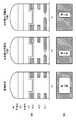
本第2の実施形態における画素の配置は、例えば図13に示すようにする。図13において、「A」と記載された画素は位相差AF用画素のうち基準画像(A像)を形成する画素、「B」と記載された画素は位相差AF画素のうち参照画像(B像)を形成する画素、その他の画素は撮像用画素である。撮像用画素のうち、上の2行はスキャンAFに用い、下の2行はEVF用に用いるものとする。 The pixel arrangement in the second embodiment is, for example, as shown in FIG. In FIG. 13, a pixel described as “A” is a pixel forming a standard image (A image) among the pixels for phase difference AF, and a pixel described as “B” is a reference image (B The image forming pixels and other pixels are imaging pixels. Of the imaging pixels, the upper two rows are used for scan AF, and the lower two rows are used for EVF.
なお、画素の配置を除く撮像装置の構成は、第1の実施形態で説明したものと同様であるので、ここでは説明を省略する。 Note that the configuration of the imaging apparatus excluding the pixel arrangement is the same as that described in the first embodiment, and a description thereof will be omitted here.
本第2の実施形態においては、図14に示すタイミングチャートに示すタイミングで撮像素子5を駆動する。まず、EVF用の画素、スキャンAF用の画素、位相差AF用画素は、TX信号及びRS信号が共に立ち上がることによって、フォトダイオード202の電荷がリセットされ、TX信号がローになると電荷蓄積が開始される。この動作はTG16によって設定された条件で順次行われる。
In the second embodiment, the
その後、スキャンAF用の行において、所定の電荷蓄積時間の経過後に、TX5信号及びTX6信号が順次立ち上がり、フォトダイオード202に蓄積された電荷を転送トランジスタ203を介して信号増幅アンプ204に読み出す。読み出した電荷は、水平走査回路209を通して出力され、スキャンAF用の画像信号を取得する。その後、再度TX5, RS5信号及びTX6, RS6信号が順次立ち上がり、スキャンAF用の行をリセットする。スキャンAF用の画像信号を取得するため、この動作を繰り返す。
Thereafter, in a row for scan AF, after a predetermined charge accumulation time elapses, the TX5 signal and the TX6 signal sequentially rise, and the charge accumulated in the
同様に、EVF用の電荷蓄積時間の経過後に、TX1信号及びTX2信号が順次立ち上がり、フォトダイオード202の電荷を転送トランジスタ203を介して信号増幅アンプ204に読み出す。読み出した電荷は、水平走査回路209を通して出力され、EVF用の画像信号を取得する。その後、再度TX1, RS1信号及びTX2, RS2信号が順次立ち上がり、EVF用の行をリセットする。EVF用の画像信号を取得するためこの動作を繰り返す。なお、図14に示す例では、第1の実施形態と同様に、1垂直同期期間にEVF用の画像信号を3回読み出しているが、そのうち1回の画像信号をLCD10に表示し、それ以外は読み捨てる。
Similarly, after the EVF charge accumulation time has elapsed, the TX1 signal and the TX2 signal sequentially rise, and the charge of the
同様に、位相差AF用の電荷蓄積時間の経過後に、TX3信号及びTX4信号が順次立ち上がり、フォトダイオード202の電荷を転送トランジスタ203を介して信号増幅アンプ204に読み出し、水平走査回路209を通して出力する。こうして、位相差AF用の画像信号を取得する。
Similarly, after the charge accumulation time for phase difference AF elapses, the TX3 signal and the TX4 signal sequentially rise, read the charge of the
このように駆動された撮像素子5からの出力信号を用いた動作は第1の実施形態と同様に図7に示す手順で行われる。但し、第2の実施形態では、スキャンAF用の画素を有するため、S7(センサー駆動タイミングの変更)の処理は行われない。また、各信号を得るための露出条件の決めた方も第1の実施形態と同様である。そして定められた露光条件で位相差AF処理及びスキャンAF処理を行い合焦位置を求める。具体的な処理の内容は第1の実施形態と同様である。
The operation using the output signal from the
上記の通り本第2の実施形態によれば、第1の実施形態と同様の効果を得ることができると共に、EVF用、スキャンAF用、位相差AF用の画像信号を並行して得ることができるため、駆動方法の切替えが不要になり、より高速に焦点調節を行うことができる。 As described above, according to the second embodiment, the same effects as those of the first embodiment can be obtained, and image signals for EVF, scan AF, and phase difference AF can be obtained in parallel. Therefore, it is not necessary to switch the driving method, and the focus adjustment can be performed at a higher speed.
また、スキャンAFを行い、SW1前に概略の合焦位置を得ることにより、SW1後に撮影準備に係る時間を短縮することができる。 Further, by performing scan AF and obtaining an approximate in-focus position before SW1, the time required for shooting preparation after SW1 can be shortened.
第1の実施形態及び第2の実施形態ではコンパクトタイプのデジタルカメラを例に説明したが、本発明は、デジタルビデオカメラやデジタル一眼レフのライブビュー時、携帯端末のカメラ機能を用いた際等のAFにも適用可能である。 In the first and second embodiments, a compact digital camera has been described as an example. However, the present invention can be applied to a digital video camera or a digital SLR live view, when a camera function of a mobile terminal is used, or the like. It can also be applied to AF.
<第3の実施形態>
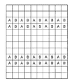
次に、本発明の第3の実施形態について説明する。第3の実施形態と第1及び第2の実施形態との違いは、撮像素子5において、位相差AF用画素が、図15に示すように配置されている点である。第3の実施形態においては、位相差AF用画素が1行に1画素置きに配置され、かつ位相差AF用画素が配置された行が連続していない。図15において、「A」と記載された画素は位相差AF用画素のうち基準画像(A像)を形成する画素、「B」と記載された画素は位相差AF画素のうち参照画像(B像)を形成する画素、その他の画素は撮像用画素である。なお、画素の配置を除く撮像装置の構成は、第1の実施形態で説明したものと同様であるので、ここでは説明を省略する。
<Third Embodiment>
Next, a third embodiment of the present invention will be described. The difference between the third embodiment and the first and second embodiments is that the phase difference AF pixels are arranged as shown in FIG. In the third embodiment, every other pixel for phase difference AF is arranged in one row, and the rows in which the pixels for phase difference AF are arranged are not continuous. In FIG. 15, a pixel described as “A” is a pixel forming a standard image (A image) among the pixels for phase difference AF, and a pixel described as “B” is a reference image (B The image forming pixels and other pixels are imaging pixels. Note that the configuration of the imaging apparatus excluding the pixel arrangement is the same as that described in the first embodiment, and a description thereof will be omitted here.
本第3の実施形態では、上記構成を有する撮像素子5を図8に示すタイミングチャートに示すタイミングで駆動する。その際に、位相差AF用画素を含む行が、図8のRS3、TX3、RS4、TX4信号により駆動されるようにする。このように駆動することで、EVF用の行と位相差AF用の行とが、交互に設定されることになる。
In the third embodiment, the
また、本第3の実施形態における撮像動作は、第1の実施形態で説明したものと比較して、図10のS503における処理が異なる以外は同様であるため、ここでは当該処理について説明する。 Further, the imaging operation in the third embodiment is the same as that described in the first embodiment except that the processing in S503 in FIG. 10 is different, and thus the processing will be described here.
S502において記録された位相差AF用の画像信号の修正を行った後、S503において、図15で「A」と記載された画素からの画像信号だけを抽出し、抽出した順序に並べて基準画像(A像)とする。同様に、「B」と記載された画素からの画像信号だけを抽出し、抽出した順序に並べて参照画像(B像)とする。このようにして得られた基準画像(A像)及び参照画像(B像)に基づいて、位相差AF処理を行う。 After correcting the image signal for phase difference AF recorded in S502, in S503, only the image signal from the pixel described as “A” in FIG. 15 is extracted, and arranged in the extracted order to display the reference image ( A image). Similarly, only the image signal from the pixel described as “B” is extracted and arranged in the extracted order as a reference image (B image). Based on the standard image (A image) and the reference image (B image) thus obtained, the phase difference AF process is performed.
第3の実施形態でEVF表示に用いるのは、EVF用の行から読み出された画像信号のみである。位相差AF用の行の撮像用画素から出力された画像信号は、露光量がEVF用としては適正でなく過露光であるが、EVF表示には用いられないので問題はない。 In the third embodiment, only the image signal read from the EVF row is used for EVF display. The image signal output from the imaging pixels in the row for phase difference AF is not appropriate for EVF and is overexposed, but there is no problem because it is not used for EVF display.
上記の通り本第3の実施形態によれば、第1の実施形態と同様の効果を得ることができる。 As described above, according to the third embodiment, the same effect as that of the first embodiment can be obtained.
なお、本発明における位相差AF用画素の配置は、第1〜第3の実施形態で説明したものに限るものではなく、位相差AF用画素を含む行と含まない行とを設けてあればよい。その場合、少なくとも位相差AF用画素を含む行を含む行を、図8のRS3、TX3、RS4、TX4信号が示す位相差AF用のタイミングで駆動し、それ以外の位相差AF用画素を含まない行は、図8のRS1、TX1、RS2、TX2信号が示すEVF用のタイミングで駆動する。そして、位相差AF用のタイミングで駆動された位相差AF用画素を含む行から出力された画像信号のうち、位相差AF用画素から出力された画像信号を抽出して位相差AFを行う。また、EVF用のタイミングで駆動された位相差AF用画素を含まない行から出力された画像信号をEVF表示に用いる。 Note that the arrangement of the phase difference AF pixels in the present invention is not limited to that described in the first to third embodiments, provided that a row including the phase difference AF pixels and a row not including the phase difference AF pixels are provided. Good. In that case, at least the row including the row including the phase difference AF pixel is driven at the timing for phase difference AF indicated by the RS3, TX3, RS4, and TX4 signals in FIG. 8, and the other phase difference AF pixels are included. The non-row rows are driven at the EVF timing indicated by the RS1, TX1, RS2, and TX2 signals in FIG. Then, the phase difference AF is performed by extracting the image signal output from the phase difference AF pixel from the image signal output from the row including the phase difference AF pixel driven at the phase difference AF timing. Further, an image signal output from a row that does not include the phase difference AF pixels driven at the EVF timing is used for EVF display.
また、上述した第1〜第3の実施形態では、フォーカスレンズ群3を駆動して焦点調節を行うものとして説明したが、撮像素子5を光軸方向に移動することにより焦点調節を行うものも、本発明の範疇に含まれる。
In the first to third embodiments described above, the
Claims (12)
測光手段と、
前記測光手段による測光結果に基づいて、前記撮像用画素のための第1の電荷蓄積時間と、前記焦点検出用画素のための第2の電荷蓄積時間とを演算する演算手段と、
前記焦点検出用画素を含まない予め決められた数の行を前記第1の電荷蓄積時間で駆動し、前記焦点検出用画素を含む行を含む予め決められた数の行を前記第2の電荷蓄積時間で駆動する駆動手段と、
前記第1の電荷蓄積時間で駆動された行の前記撮像用画素から得られた画像信号を周期的に更新して表示する表示手段と、
前記第2の電荷蓄積時間で駆動された行の前記焦点検出用画素から得られた画像信号に基づいて、位相差方式の焦点検出処理を行う第1の焦点検出手段と、
前記第1の焦点検出手段による焦点検出ができなかった場合に、前記焦点検出用画素を含まない予め決められた数の行の前記撮像用画素から得られた画像信号の高周波成分に基づいて焦点検出処理を行う第2の焦点検出手段と、を有し、
前記第2の電荷蓄積時間は、前記第1の電荷蓄積時間より長く、
前記第1の焦点検出手段による焦点検出ができなかった場合に、前記焦点調節手段を光軸方向に駆動しながら、前記駆動手段は、前記焦点検出用画素を含まない予め決められた数の行を、前記第1の電荷蓄積時間の代わりに、第3の電荷蓄積時間で駆動することを特徴とする撮像装置。 A row including a focus detection pixel that photoelectrically converts a pair of lights that pass through different exit pupil regions of the imaging optical system and outputs an image signal, and does not include the focus detection pixel. An imaging device having a row of imaging pixels;
Photometric means;
An arithmetic means for calculating a first charge accumulation time for the imaging pixel and a second charge accumulation time for the focus detection pixel based on a photometric result by the photometry means;
A predetermined number of rows not including the focus detection pixels are driven with the first charge accumulation time, and a predetermined number of rows including the focus detection pixels are included in the second charge. Driving means for driving in the accumulation time;
Display means for periodically updating and displaying an image signal obtained from the imaging pixels in a row driven by the first charge accumulation time;
First focus detection means for performing a phase difference type focus detection process based on an image signal obtained from the focus detection pixels in a row driven in the second charge accumulation time ;
When focus detection cannot be performed by the first focus detection means, the focus is based on the high-frequency component of the image signal obtained from the imaging pixels in a predetermined number of rows not including the focus detection pixels. Second focus detection means for performing detection processing ,
The second charge accumulation time is rather longer than the first charge accumulation time,
When the focus detection by the first focus detection unit cannot be performed, the drive unit drives the focus adjustment unit in the optical axis direction, and the drive unit includes a predetermined number of rows not including the focus detection pixels. Is driven with a third charge accumulation time instead of the first charge accumulation time .
前記測光手段による測光結果に基づいて、前記撮像用画素から予め決められた範囲の輝度の信号が得られる前記第1の電荷蓄積時間を求める第1の演算手段と、
前記第1の演算手段により求めた前記第1の電荷蓄積時間から、前記焦点検出用画素が前記一対の光のいずれかを受光する受光領域の開口率及び前記焦点検出用画素の像高による減光量の少なくともいずれか一方に基づいて、前記焦点検出用画素のための前記第2の電荷蓄積時間を求める第2の演算手段と
を有することを特徴とする請求項1に記載の撮像装置。 The computing means is
First computing means for obtaining the first charge accumulation time for obtaining a signal of a luminance in a predetermined range from the imaging pixels based on a photometric result by the photometric means;
From the first charge accumulation time obtained by the first computing means, the aperture detection ratio of the light receiving area where the focus detection pixel receives one of the pair of light and the image height of the focus detection pixel are reduced. The imaging apparatus according to claim 1, further comprising: a second calculation unit that obtains the second charge accumulation time for the focus detection pixel based on at least one of the light amounts.
前記第2の演算手段は、前記求めた第2の電荷蓄積時間が、前記表示手段により前記画像信号を更新して表示する周期よりも長いかどうかを判断し、長い場合に、前記第2の電荷蓄積時間を前記周期に制限し、
前記増幅手段は、前記制限により短縮された時間に対応する増幅率を、前記焦点検出用画素から得られた画像信号にかけることを特徴とする請求項2または3に記載の撮像装置。 A further amplifying means;
The second calculation means determines whether or not the obtained second charge accumulation time is longer than a period for updating and displaying the image signal by the display means. Limit the charge accumulation time to the period,
The imaging apparatus according to claim 2, wherein the amplifying unit applies an amplification factor corresponding to the time shortened by the limitation to the image signal obtained from the focus detection pixel.
前記増幅手段は、前記制限により短縮された時間に対応する増幅率を、前記焦点検出用画素から得られた画像信号にかけることを特徴とする請求項4に記載の撮像装置。 The second calculation means determines whether or not the obtained second charge accumulation time is longer than an upper limit time determined in advance according to a focal length of the imaging optical system. Limiting the second charge accumulation time to the upper limit time;
The imaging apparatus according to claim 4, wherein the amplifying unit applies an amplification factor corresponding to the time shortened by the restriction to the image signal obtained from the focus detection pixel.
前記増幅手段は、前記制限により短縮された時間に対応する増幅率を、前記焦点検出用画素から得られた画像信号にかけることを特徴とする請求項4または5に記載の撮像装置。 The second calculation means determines whether or not there is a focus detection pixel that saturates when driven by the obtained second charge storage time, and if it is determined that there is, the second charge storage Limit time to the time when focus detection pixels are not saturated,
The imaging apparatus according to claim 4, wherein the amplifying unit applies an amplification factor corresponding to the time shortened by the limitation to the image signal obtained from the focus detection pixel.
前記設定された焦点検出領域に点光源被写体が存在するかどうかを判定する手段とを更に有し、
前記設定された焦点検出領域に前記点光源被写体が存在すると判定された場合に、前記第2の演算手段は、前記求めた第2の電荷蓄積時間を焦点検出用画素が飽和しない時間に調整し、
前記増幅手段は、前記調整により短縮された時間に対応する増幅率を、前記焦点検出用画素から得られた画像信号にかけることを特徴とする請求項4乃至6のいずれか1項に記載の撮像装置。 Means for setting a focus detection area;
Means for determining whether a point light source subject is present in the set focus detection area;
When it is determined that the point light source subject is present in the set focus detection area, the second calculation means adjusts the obtained second charge accumulation time to a time at which the focus detection pixels are not saturated. ,
7. The amplifier according to claim 4, wherein the amplifying unit applies an amplification factor corresponding to the time shortened by the adjustment to the image signal obtained from the focus detection pixel. 8. Imaging device.
前記駆動手段は、前記第2の電荷蓄積時間で駆動された行のうち、前記設定された焦点検出領域に含まれる画素から画像信号を読み出すことを特徴とする請求項1乃至9のいずれか1項に記載の撮像装置。 A means for setting a focus detection area;
The drive means of the rows driven by the second charge accumulation time, any one of claims 1 to 9, characterized in that reading the image signals from the pixels included in the set focus detection area was 1 The imaging device according to item.
測光手段により測光を行う測光工程と、
演算手段が、前記測光工程の測光結果に基づいて、前記撮像用画素のための第1の電荷蓄積時間と、前記焦点検出用画素のための第2の電荷蓄積時間とを演算する演算工程と、
駆動手段が、前記焦点検出用画素を含まない予め決められた数の行を前記第1の電荷蓄積時間で駆動し、前記焦点検出用画素を含む行を含む予め決められた数の行を前記第2の電荷蓄積時間で駆動する駆動工程と、
表示手段が、前記第1の電荷蓄積時間で駆動された行の前記撮像用画素から得られた画像信号を周期的に更新して表示する表示工程と、
第1の焦点検出手段が、前記第2の電荷蓄積時間で駆動された行の前記焦点検出用画素から得られた画像信号に基づいて、位相差方式の焦点検出処理を行う第1の焦点検出工程と、
前記第1の焦点検出手段による焦点検出ができなかった場合に、前記焦点検出用画素を含まない予め決められた数の行の前記撮像用画素から得られた画像信号の高周波成分に基づいて焦点検出処理を行う第2の焦点検出工程と、を有し、
前記第2の電荷蓄積時間は、前記第1の電荷蓄積時間より長く、
前記駆動工程において、前記第1の焦点検出手段による焦点検出ができなかった場合に、前記焦点調節手段を光軸方向に駆動しながら、前記焦点検出用画素を含まない予め決められた数の行を、前記第1の電荷蓄積時間の代わりに、第3の電荷蓄積時間で駆動することを特徴とする撮像装置の制御方法。 A row including a focus detection pixel that photoelectrically converts a pair of lights that pass through different exit pupil regions of the imaging optical system and outputs an image signal, and does not include the focus detection pixel. A method for controlling an imaging apparatus having an imaging element having a row of imaging pixels,
A photometric process for performing photometry with a photometric means;
A calculating step for calculating a first charge accumulation time for the imaging pixel and a second charge accumulation time for the focus detection pixel based on the photometric result of the photometry step; ,
The driving means drives a predetermined number of rows not including the focus detection pixels with the first charge accumulation time, and determines a predetermined number of rows including the rows including the focus detection pixels. A driving step of driving with a second charge accumulation time;
A display step in which the display means periodically updates and displays the image signal obtained from the imaging pixels in the row driven by the first charge accumulation time;
The first focus detection unit, based on an image signal obtained from the focus detection pixels of rows driven by the second charge accumulation time, a first focus detection performing focus detection processing of the phase difference method Process ,
When focus detection cannot be performed by the first focus detection means, the focus is based on the high-frequency component of the image signal obtained from the imaging pixels in a predetermined number of rows not including the focus detection pixels. A second focus detection step for performing a detection process ,
The second charge accumulation time is rather longer than the first charge accumulation time,
In the driving step, when focus detection cannot be performed by the first focus detection unit, a predetermined number of rows not including the focus detection pixels are driven while driving the focus adjustment unit in the optical axis direction. Is driven with a third charge accumulation time instead of the first charge accumulation time .
Priority Applications (3)
| Application Number | Priority Date | Filing Date | Title |
|---|---|---|---|
| JP2013202233A JP6257245B2 (en) | 2013-09-27 | 2013-09-27 | Imaging apparatus and control method thereof |
| US14/495,187 US9426350B2 (en) | 2013-09-27 | 2014-09-24 | Image capturing apparatus and control method thereof |
| CN201410509770.9A CN104519276B (en) | 2013-09-27 | 2014-09-28 | The control method of picture pick-up device and picture pick-up device |
Applications Claiming Priority (1)
| Application Number | Priority Date | Filing Date | Title |
|---|---|---|---|
| JP2013202233A JP6257245B2 (en) | 2013-09-27 | 2013-09-27 | Imaging apparatus and control method thereof |
Publications (3)
| Publication Number | Publication Date |
|---|---|
| JP2015068959A JP2015068959A (en) | 2015-04-13 |
| JP2015068959A5 JP2015068959A5 (en) | 2016-11-10 |
| JP6257245B2 true JP6257245B2 (en) | 2018-01-10 |
Family
ID=52739803
Family Applications (1)
| Application Number | Title | Priority Date | Filing Date |
|---|---|---|---|
| JP2013202233A Active JP6257245B2 (en) | 2013-09-27 | 2013-09-27 | Imaging apparatus and control method thereof |
Country Status (3)
| Country | Link |
|---|---|
| US (1) | US9426350B2 (en) |
| JP (1) | JP6257245B2 (en) |
| CN (1) | CN104519276B (en) |
Families Citing this family (30)
| Publication number | Priority date | Publication date | Assignee | Title |
|---|---|---|---|---|
| WO2015016085A1 (en) * | 2013-08-01 | 2015-02-05 | 富士フイルム株式会社 | Photographing method and apparatus |
| KR102124598B1 (en) * | 2013-09-30 | 2020-06-19 | 삼성전자주식회사 | Image acquisition method and apparatus |
| EP3054667A4 (en) * | 2013-10-01 | 2017-11-15 | Nikon Corporation | Electronic apparatus |
| JP6146293B2 (en) * | 2013-12-25 | 2017-06-14 | ソニー株式会社 | Control device, control method, and control system |
| JP6214421B2 (en) * | 2014-02-18 | 2017-10-18 | オリンパス株式会社 | Imaging apparatus and imaging method |
| JP2016038414A (en) * | 2014-08-05 | 2016-03-22 | キヤノン株式会社 | Focus detection device, control method thereof, and imaging apparatus |
| JP6218799B2 (en) | 2015-01-05 | 2017-10-25 | キヤノン株式会社 | Imaging device and imaging apparatus |
| US10070088B2 (en) | 2015-01-05 | 2018-09-04 | Canon Kabushiki Kaisha | Image sensor and image capturing apparatus for simultaneously performing focus detection and image generation |
| JP6494333B2 (en) * | 2015-03-04 | 2019-04-03 | キヤノン株式会社 | Image processing apparatus, image processing method, and imaging apparatus |
| JP6595797B2 (en) * | 2015-05-12 | 2019-10-23 | キヤノン株式会社 | Imaging apparatus and control method thereof |
| JP6476065B2 (en) * | 2015-05-14 | 2019-02-27 | オリンパス株式会社 | IMAGING DEVICE AND IMAGING DEVICE CONTROL METHOD |
| JP6504969B2 (en) * | 2015-08-19 | 2019-04-24 | キヤノン株式会社 | Imaging system, imaging apparatus, lens apparatus, control method of imaging system |
| WO2017039038A1 (en) * | 2015-09-04 | 2017-03-09 | 재단법인 다차원 스마트 아이티 융합시스템 연구단 | Image sensor to which multiple fill factors are applied |
| WO2017047010A1 (en) * | 2015-09-16 | 2017-03-23 | Canon Kabushiki Kaisha | Image sensor and image capturing apparatus |
| DE112016004211T5 (en) | 2015-09-16 | 2018-06-14 | Canon Kabushiki Kaisha | Image sensor and image pickup device |
| JP2017118296A (en) * | 2015-12-24 | 2017-06-29 | キヤノン株式会社 | Imaging apparatus, image processing apparatus, image processing method, image processing program, and storage medium |
| JP6748454B2 (en) | 2016-03-10 | 2020-09-02 | キヤノン株式会社 | Imaging device, control method thereof, program, and storage medium |
| JP6723774B2 (en) * | 2016-03-15 | 2020-07-15 | キヤノン株式会社 | Imaging device, imaging device, distance measuring device, and moving body |
| US9930243B2 (en) | 2016-05-02 | 2018-03-27 | Mitutoyo Corporation | Variable focal length imaging system |
| US9736355B1 (en) * | 2016-05-03 | 2017-08-15 | Mitutoyo Corporation | Phase difference calibration in a variable focal length lens system |
| CN109937382B (en) | 2016-08-26 | 2020-12-18 | 华为技术有限公司 | Image forming apparatus and image forming method |
| WO2018088119A1 (en) * | 2016-11-09 | 2018-05-17 | 富士フイルム株式会社 | Imaging device, imaging method, and imaging program |
| JP2018081224A (en) * | 2016-11-17 | 2018-05-24 | キヤノン株式会社 | Imaging device and control method thereof |
| JP6265253B1 (en) * | 2016-12-15 | 2018-01-24 | オムロン株式会社 | Inspection apparatus and inspection method |
| JP2018152696A (en) * | 2017-03-13 | 2018-09-27 | ソニーセミコンダクタソリューションズ株式会社 | Solid state image sensor, driving method thereof and electronic equipment |
| JP6929106B2 (en) | 2017-04-07 | 2021-09-01 | キヤノン株式会社 | Imaging device and control method of imaging device |
| JP6643291B2 (en) * | 2017-09-22 | 2020-02-12 | キヤノン株式会社 | Imaging device and driving method thereof |
| CN109698902B (en) * | 2017-10-24 | 2020-09-11 | 华为技术有限公司 | Synchronous focusing method and device |
| CN113329146B (en) * | 2021-04-25 | 2022-06-03 | 北京大学 | Pulse camera simulation method and device |
| JP2023051391A (en) | 2021-09-30 | 2023-04-11 | 富士フイルム株式会社 | Imaging device, imaging control method, and imaging control program |
Family Cites Families (44)
| Publication number | Priority date | Publication date | Assignee | Title |
|---|---|---|---|---|
| JP2620235B2 (en) | 1987-04-24 | 1997-06-11 | キヤノン株式会社 | Signal forming device |
| JP2883691B2 (en) | 1990-07-06 | 1999-04-19 | オリンパス光学工業株式会社 | Camera automatic exposure control device |
| JP3105334B2 (en) | 1992-03-11 | 2000-10-30 | 三菱電機株式会社 | Automatic focusing device |
| JPH08265631A (en) | 1995-03-27 | 1996-10-11 | Canon Inc | Automatic focus adjustment device |
| JP2000078461A (en) | 1998-08-28 | 2000-03-14 | Casio Comput Co Ltd | Device and method for controlling exposure |
| JP2001021792A (en) * | 1999-07-09 | 2001-01-26 | Olympus Optical Co Ltd | Focus detection system |
| JP2001305423A (en) * | 2000-04-19 | 2001-10-31 | Nikon Corp | Range finder |
| JP4565370B2 (en) | 2000-12-22 | 2010-10-20 | 富士フイルム株式会社 | Electronic camera and autofocus control method |
| EP1294069B2 (en) | 2001-09-18 | 2015-04-01 | ABB Technology AG | Electronic circuit breaker |
| JP4235422B2 (en) | 2002-09-06 | 2009-03-11 | キヤノン株式会社 | FOCUS DETECTION METHOD, FOCUS DETECTION DEVICE, AND IMAGING DEVICE |
| JP4266726B2 (en) * | 2003-05-30 | 2009-05-20 | キヤノン株式会社 | Imaging device |
| JP4259998B2 (en) | 2003-12-19 | 2009-04-30 | 三洋電機株式会社 | Flicker detection device and imaging device |
| JP2006184320A (en) * | 2004-12-24 | 2006-07-13 | Canon Inc | Focus detecting device and focus detecting method |
| JP4377840B2 (en) | 2005-03-31 | 2009-12-02 | イーストマン コダック カンパニー | Digital camera |
| JP4588583B2 (en) | 2005-08-29 | 2010-12-01 | 富士フイルム株式会社 | Imaging apparatus and focus control method |
| JP4872277B2 (en) | 2005-09-05 | 2012-02-08 | ソニー株式会社 | Imaging apparatus and imaging method |
| JP4742242B2 (en) | 2005-09-30 | 2011-08-10 | カシオ計算機株式会社 | Imaging apparatus and program thereof |
| JP4801960B2 (en) | 2005-10-05 | 2011-10-26 | 株式会社リコー | Autofocus control device, image forming apparatus using the autofocus control device, and autofocus control method |
| JP2007212723A (en) | 2006-02-09 | 2007-08-23 | Fujifilm Corp | Focusing position determination method and device |
| JP2007212745A (en) | 2006-02-09 | 2007-08-23 | Canon Inc | Light control filter |
| JP4946313B2 (en) * | 2006-09-27 | 2012-06-06 | 株式会社ニコン | Imaging device |
| JP2008130531A (en) | 2006-11-27 | 2008-06-05 | Matsushita Electric Works Ltd | Push button structure, and wall remote control using it for toilet |
| US7859588B2 (en) | 2007-03-09 | 2010-12-28 | Eastman Kodak Company | Method and apparatus for operating a dual lens camera to augment an image |
| JP5098405B2 (en) * | 2007-04-11 | 2012-12-12 | 株式会社ニコン | Imaging device, focus detection device, and imaging device |
| JP4936534B2 (en) | 2007-06-11 | 2012-05-23 | キヤノン株式会社 | Imaging apparatus and focus control method |
| US7809260B2 (en) | 2007-08-02 | 2010-10-05 | Canon Kabushiki Kaisha | Image capturing apparatus and method for controlling same |
| JP2009049858A (en) * | 2007-08-22 | 2009-03-05 | Canon Inc | Imaging apparatus |
| JP2010091943A (en) * | 2008-10-10 | 2010-04-22 | Canon Inc | Imaging apparatus |
| JP2010122301A (en) * | 2008-11-17 | 2010-06-03 | Hitachi Ltd | Focus control device and focus control method |
| JP5400406B2 (en) * | 2009-02-06 | 2014-01-29 | キヤノン株式会社 | Imaging device |
| JP5319347B2 (en) * | 2009-03-17 | 2013-10-16 | キヤノン株式会社 | Imaging apparatus and control method thereof |
| JP5704851B2 (en) | 2009-12-25 | 2015-04-22 | キヤノン株式会社 | IMAGING DEVICE, IMAGING DEVICE CONTROL METHOD, AND COMPUTER PROGRAM |
| US20120120277A1 (en) | 2010-11-16 | 2012-05-17 | Apple Inc. | Multi-point Touch Focus |
| JP2012113189A (en) * | 2010-11-26 | 2012-06-14 | Nikon Corp | Imaging apparatus |
| JP5901246B2 (en) * | 2010-12-13 | 2016-04-06 | キヤノン株式会社 | Imaging device |
| KR20120081514A (en) | 2011-01-11 | 2012-07-19 | 삼성전자주식회사 | Moving picture photographing control method and apparatus |
| JP5791285B2 (en) | 2011-02-02 | 2015-10-07 | キヤノン株式会社 | Imaging apparatus, focus adjustment method, program |
| JP5850648B2 (en) | 2011-06-06 | 2016-02-03 | キヤノン株式会社 | Imaging device |
| JP2013068819A (en) * | 2011-09-22 | 2013-04-18 | Olympus Imaging Corp | Imaging apparatus and light quantity control device |
| JP5959829B2 (en) * | 2011-11-09 | 2016-08-02 | キヤノン株式会社 | Solid-state imaging device |
| JP5932474B2 (en) | 2012-05-09 | 2016-06-08 | キヤノン株式会社 | Imaging apparatus and control method thereof |
| JP6149369B2 (en) | 2012-09-27 | 2017-06-21 | 株式会社ニコン | Image sensor |
| EP2782331A1 (en) * | 2013-03-22 | 2014-09-24 | Harvest Imaging bvba | Image sensor with focus-detection pixel, and method for reading focus-information |
| JP6234261B2 (en) | 2014-02-10 | 2017-11-22 | オリンパス株式会社 | Focus adjustment apparatus and control method |
-
2013
- 2013-09-27 JP JP2013202233A patent/JP6257245B2/en active Active
-
2014
- 2014-09-24 US US14/495,187 patent/US9426350B2/en active Active
- 2014-09-28 CN CN201410509770.9A patent/CN104519276B/en not_active Expired - Fee Related
Also Published As
| Publication number | Publication date |
|---|---|
| CN104519276A (en) | 2015-04-15 |
| US9426350B2 (en) | 2016-08-23 |
| CN104519276B (en) | 2018-05-11 |
| US20150092098A1 (en) | 2015-04-02 |
| JP2015068959A (en) | 2015-04-13 |
Similar Documents
| Publication | Publication Date | Title |
|---|---|---|
| JP6257245B2 (en) | Imaging apparatus and control method thereof | |
| JP6539015B2 (en) | Image pickup apparatus and control method thereof | |
| US8175447B2 (en) | Image pickup apparatus and control method therefor | |
| JP6555857B2 (en) | Imaging apparatus and control method thereof | |
| US9197809B2 (en) | Image pickup apparatus, method of controlling image pickup apparatus, and non-transitory computer-readable storage medium | |
| JP6116277B2 (en) | Imaging apparatus and control method thereof | |
| JP6518452B2 (en) | Imaging apparatus and imaging method | |
| JP6944846B2 (en) | Imaging device, control method of imaging device | |
| US9654680B2 (en) | Image capturing apparatus and control method therefor | |
| JP2012063396A (en) | Focus adjustment device | |
| JP2009124313A (en) | Electronic camera | |
| JP5100410B2 (en) | Imaging apparatus and control method thereof | |
| JP2015111252A (en) | Imaging device, imaging device control method, program, and storage medium | |
| JP2015031743A (en) | Exposure control device, control method for the same, and control program, and imaging device | |
| JP2013113857A (en) | Imaging device, and control method therefor | |
| JP6727933B2 (en) | Imaging device and control method | |
| JP2016213757A (en) | Imaging apparatus and control method of the same | |
| JP2015152742A (en) | Imaging device and control method thereof | |
| JP2018006828A (en) | Imaging apparatus, control method therefor and program | |
| US20200412966A1 (en) | Focus adjustment device and focus adjustment method | |
| JP2014171145A (en) | Image pickup device, image pickup method, and program therefor | |
| JP6305016B2 (en) | FOCUS CONTROL DEVICE, FOCUS CONTROL DEVICE CONTROL METHOD, AND IMAGING DEVICE | |
| JP2008283477A (en) | Image processor, and image processing method | |
| JP2015152830A (en) | Imaging device and control method thereof, program, and storage medium | |
| JP2016006940A (en) | Camera with contrast af function |
Legal Events
| Date | Code | Title | Description |
|---|---|---|---|
| A521 | Request for written amendment filed |
Free format text: JAPANESE INTERMEDIATE CODE: A523 Effective date: 20160916 |
|
| A621 | Written request for application examination |
Free format text: JAPANESE INTERMEDIATE CODE: A621 Effective date: 20160916 |
|
| A977 | Report on retrieval |
Free format text: JAPANESE INTERMEDIATE CODE: A971007 Effective date: 20170419 |
|
| A131 | Notification of reasons for refusal |
Free format text: JAPANESE INTERMEDIATE CODE: A131 Effective date: 20170602 |
|
| A521 | Request for written amendment filed |
Free format text: JAPANESE INTERMEDIATE CODE: A523 Effective date: 20170728 |
|
| TRDD | Decision of grant or rejection written | ||
| A01 | Written decision to grant a patent or to grant a registration (utility model) |
Free format text: JAPANESE INTERMEDIATE CODE: A01 Effective date: 20171106 |
|
| A61 | First payment of annual fees (during grant procedure) |
Free format text: JAPANESE INTERMEDIATE CODE: A61 Effective date: 20171205 |
|
| R151 | Written notification of patent or utility model registration |
Ref document number: 6257245 Country of ref document: JP Free format text: JAPANESE INTERMEDIATE CODE: R151 |