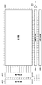
JP5319347B2 - Imaging apparatus and control method thereof - Google Patents
Imaging apparatus and control method thereof Download PDFInfo
- Publication number
- JP5319347B2 JP5319347B2 JP2009065221A JP2009065221A JP5319347B2 JP 5319347 B2 JP5319347 B2 JP 5319347B2 JP 2009065221 A JP2009065221 A JP 2009065221A JP 2009065221 A JP2009065221 A JP 2009065221A JP 5319347 B2 JP5319347 B2 JP 5319347B2
- Authority
- JP
- Japan
- Prior art keywords
- imaging
- focus detection
- pixels
- image
- row
- Prior art date
- Legal status (The legal status is an assumption and is not a legal conclusion. Google has not performed a legal analysis and makes no representation as to the accuracy of the status listed.)
- Active
Links
- 238000003384 imaging method Methods 0.000 title claims abstract description 94
- 238000000034 method Methods 0.000 title claims description 19
- 238000001514 detection method Methods 0.000 claims abstract description 126
- 238000009825 accumulation Methods 0.000 claims abstract description 35
- 210000001747 pupil Anatomy 0.000 claims abstract description 27
- 230000003287 optical effect Effects 0.000 description 19
- 238000005096 rolling process Methods 0.000 description 17
- 238000010586 diagram Methods 0.000 description 16
- 238000006243 chemical reaction Methods 0.000 description 8
- 230000006870 function Effects 0.000 description 6
- 230000035945 sensitivity Effects 0.000 description 6
- 230000007423 decrease Effects 0.000 description 3
- 238000009792 diffusion process Methods 0.000 description 3
- 238000011156 evaluation Methods 0.000 description 3
- 238000007667 floating Methods 0.000 description 3
- 238000012546 transfer Methods 0.000 description 3
- 239000003990 capacitor Substances 0.000 description 2
- 230000015556 catabolic process Effects 0.000 description 2
- 230000002950 deficient Effects 0.000 description 2
- 238000006731 degradation reaction Methods 0.000 description 2
- 230000006866 deterioration Effects 0.000 description 2
- 238000005286 illumination Methods 0.000 description 2
- 238000012545 processing Methods 0.000 description 2
- 230000011514 reflex Effects 0.000 description 2
- 230000003595 spectral effect Effects 0.000 description 2
- 238000003491 array Methods 0.000 description 1
- 230000008901 benefit Effects 0.000 description 1
- 238000004364 calculation method Methods 0.000 description 1
- 239000003086 colorant Substances 0.000 description 1
- 238000004891 communication Methods 0.000 description 1
- 230000006835 compression Effects 0.000 description 1
- 238000007906 compression Methods 0.000 description 1
- 238000012790 confirmation Methods 0.000 description 1
- 238000012937 correction Methods 0.000 description 1
- 230000007547 defect Effects 0.000 description 1
- 238000005516 engineering process Methods 0.000 description 1
- 230000004907 flux Effects 0.000 description 1
- 238000007429 general method Methods 0.000 description 1
- 238000005259 measurement Methods 0.000 description 1
- 238000012986 modification Methods 0.000 description 1
- 230000004048 modification Effects 0.000 description 1
- 230000002093 peripheral effect Effects 0.000 description 1
- 230000008569 process Effects 0.000 description 1
- 238000000926 separation method Methods 0.000 description 1
- GGCZERPQGJTIQP-UHFFFAOYSA-N sodium;9,10-dioxoanthracene-2-sulfonic acid Chemical compound [Na+].C1=CC=C2C(=O)C3=CC(S(=O)(=O)O)=CC=C3C(=O)C2=C1 GGCZERPQGJTIQP-UHFFFAOYSA-N 0.000 description 1
- 229910052724 xenon Inorganic materials 0.000 description 1
- FHNFHKCVQCLJFQ-UHFFFAOYSA-N xenon atom Chemical compound [Xe] FHNFHKCVQCLJFQ-UHFFFAOYSA-N 0.000 description 1
Images


Classifications
-
- H—ELECTRICITY
- H01—ELECTRIC ELEMENTS
- H01L—SEMICONDUCTOR DEVICES NOT COVERED BY CLASS H10
- H01L27/00—Devices consisting of a plurality of semiconductor or other solid-state components formed in or on a common substrate
- H01L27/14—Devices consisting of a plurality of semiconductor or other solid-state components formed in or on a common substrate including semiconductor components sensitive to infrared radiation, light, electromagnetic radiation of shorter wavelength or corpuscular radiation and specially adapted either for the conversion of the energy of such radiation into electrical energy or for the control of electrical energy by such radiation
- H01L27/144—Devices controlled by radiation
- H01L27/146—Imager structures
- H01L27/14601—Structural or functional details thereof
- H01L27/1462—Coatings
- H01L27/14621—Colour filter arrangements
-
- H—ELECTRICITY
- H01—ELECTRIC ELEMENTS
- H01L—SEMICONDUCTOR DEVICES NOT COVERED BY CLASS H10
- H01L27/00—Devices consisting of a plurality of semiconductor or other solid-state components formed in or on a common substrate
- H01L27/14—Devices consisting of a plurality of semiconductor or other solid-state components formed in or on a common substrate including semiconductor components sensitive to infrared radiation, light, electromagnetic radiation of shorter wavelength or corpuscular radiation and specially adapted either for the conversion of the energy of such radiation into electrical energy or for the control of electrical energy by such radiation
- H01L27/144—Devices controlled by radiation
- H01L27/146—Imager structures
- H01L27/14601—Structural or functional details thereof
- H01L27/14625—Optical elements or arrangements associated with the device
- H01L27/14627—Microlenses
-
- H—ELECTRICITY
- H04—ELECTRIC COMMUNICATION TECHNIQUE
- H04N—PICTORIAL COMMUNICATION, e.g. TELEVISION
- H04N23/00—Cameras or camera modules comprising electronic image sensors; Control thereof
- H04N23/60—Control of cameras or camera modules
- H04N23/67—Focus control based on electronic image sensor signals
- H04N23/672—Focus control based on electronic image sensor signals based on the phase difference signals
-
- H—ELECTRICITY
- H04—ELECTRIC COMMUNICATION TECHNIQUE
- H04N—PICTORIAL COMMUNICATION, e.g. TELEVISION
- H04N25/00—Circuitry of solid-state image sensors [SSIS]; Control thereof
- H04N25/10—Circuitry of solid-state image sensors [SSIS]; Control thereof for transforming different wavelengths into image signals
- H04N25/11—Arrangement of colour filter arrays [CFA]; Filter mosaics
- H04N25/13—Arrangement of colour filter arrays [CFA]; Filter mosaics characterised by the spectral characteristics of the filter elements
- H04N25/134—Arrangement of colour filter arrays [CFA]; Filter mosaics characterised by the spectral characteristics of the filter elements based on three different wavelength filter elements
-
- H—ELECTRICITY
- H04—ELECTRIC COMMUNICATION TECHNIQUE
- H04N—PICTORIAL COMMUNICATION, e.g. TELEVISION
- H04N25/00—Circuitry of solid-state image sensors [SSIS]; Control thereof
- H04N25/50—Control of the SSIS exposure
- H04N25/53—Control of the integration time
- H04N25/531—Control of the integration time by controlling rolling shutters in CMOS SSIS
-
- H—ELECTRICITY
- H04—ELECTRIC COMMUNICATION TECHNIQUE
- H04N—PICTORIAL COMMUNICATION, e.g. TELEVISION
- H04N25/00—Circuitry of solid-state image sensors [SSIS]; Control thereof
- H04N25/70—SSIS architectures; Circuits associated therewith
- H04N25/703—SSIS architectures incorporating pixels for producing signals other than image signals
- H04N25/704—Pixels specially adapted for focusing, e.g. phase difference pixel sets
-
- H—ELECTRICITY
- H04—ELECTRIC COMMUNICATION TECHNIQUE
- H04N—PICTORIAL COMMUNICATION, e.g. TELEVISION
- H04N25/00—Circuitry of solid-state image sensors [SSIS]; Control thereof
- H04N25/70—SSIS architectures; Circuits associated therewith
- H04N25/76—Addressed sensors, e.g. MOS or CMOS sensors
-
- H—ELECTRICITY
- H01—ELECTRIC ELEMENTS
- H01L—SEMICONDUCTOR DEVICES NOT COVERED BY CLASS H10
- H01L27/00—Devices consisting of a plurality of semiconductor or other solid-state components formed in or on a common substrate
- H01L27/14—Devices consisting of a plurality of semiconductor or other solid-state components formed in or on a common substrate including semiconductor components sensitive to infrared radiation, light, electromagnetic radiation of shorter wavelength or corpuscular radiation and specially adapted either for the conversion of the energy of such radiation into electrical energy or for the control of electrical energy by such radiation
- H01L27/144—Devices controlled by radiation
- H01L27/146—Imager structures
- H01L27/14643—Photodiode arrays; MOS imagers
-
- H—ELECTRICITY
- H04—ELECTRIC COMMUNICATION TECHNIQUE
- H04N—PICTORIAL COMMUNICATION, e.g. TELEVISION
- H04N23/00—Cameras or camera modules comprising electronic image sensors; Control thereof
- H04N23/60—Control of cameras or camera modules
- H04N23/63—Control of cameras or camera modules by using electronic viewfinders
Landscapes
- Engineering & Computer Science (AREA)
- Physics & Mathematics (AREA)
- Multimedia (AREA)
- Signal Processing (AREA)
- Power Engineering (AREA)
- Microelectronics & Electronic Packaging (AREA)
- Electromagnetism (AREA)
- Condensed Matter Physics & Semiconductors (AREA)
- General Physics & Mathematics (AREA)
- Computer Hardware Design (AREA)
- Spectroscopy & Molecular Physics (AREA)
- Studio Devices (AREA)
- Automatic Focus Adjustment (AREA)
- Transforming Light Signals Into Electric Signals (AREA)
- Focusing (AREA)
- Solid State Image Pick-Up Elements (AREA)
Abstract
Description
本発明は、2次元状に配置された多数の画素を有する撮像素子を備えた撮像装置に関するものである。 The present invention relates to an image pickup apparatus including an image pickup element having a large number of pixels arranged two-dimensionally.
撮像装置の自動焦点検出・調節方法で撮影レンズを通過した光束を用いる一般的な方式として、コントラスト検出方式(ぼけ方式と呼ばれる)と位相差検出方式(ずれ方式と呼ばれる)とがある。コントラスト検出方式は動画撮影用ビデオムービー機器(カムコーダー)や電子スチルカメラで多く用いられる方式で、撮像素子が焦点検出用センサーとして用いられるものである。撮像素子の出力信号、特に高周波成分の情報(コントラスト情報)に着目し、その評価値が最も大きくなる撮影レンズの位置を合焦位置とする方式である。しかし山登り方式とも言われるように、撮影レンズを微少量動かしながら評価値を求め、その評価値が結果的に最大であったとわかるまで動かすことが必要であるため、高速な焦点調節動作には不向きとされている。 There are a contrast detection method (called a blur method) and a phase difference detection method (called a shift method) as a general method using a light beam that has passed through a photographing lens in an automatic focus detection / adjustment method of an imaging apparatus. The contrast detection method is a method often used in video movie equipment (camcorder) for video recording and electronic still cameras, and an image sensor is used as a focus detection sensor. Focusing on the output signal of the image sensor, particularly information on high-frequency components (contrast information), the position of the photographing lens with the largest evaluation value is used as the in-focus position. However, as it is said to be a hill-climbing method, it is necessary to calculate the evaluation value while moving the photographic lens by a small amount and move it until it is determined that the evaluation value is the maximum as a result, so it is not suitable for high-speed focus adjustment operation. It is said that.
もう一方の位相差検出方式は、銀塩フィルムによる一眼レフカメラに多く用いられ、自動焦点検出(Auto Focus:AF)一眼レフカメラの実用化に最も貢献した技術である。位相差検出方式では、撮影レンズの射出瞳を通過した光束を2分割し、2分割した光束を一組の焦点検出用センサーによりそれぞれ受光し、その受光量に応じて出力される信号のずれ量、すなわち、光束の分割方向の相対的位置ずれ量を検出する。これにより、撮影レンズのピント方向のずれ量を直接求めるものである。従って、焦点検出用センサーにより一度蓄積動作を行なえばピントずれの量と方向が得られ、高速な焦点調節動作が可能となっている。但し、撮影レンズの射出瞳を通過した光束を2分割し、それぞれの光束に対応する信号を得るためには、撮像光路中にクイックリターンミラーやハーフミラー等の光路分割手段を設け、その先に焦点検出用光学系とAFセンサを設けるのが一般的である。そのため、装置が大型、かつ高価となる欠点がある。 The other phase difference detection method is often used in a single-lens reflex camera using a silver salt film, and is the technology most contributing to the practical application of an auto focus (AF) single-lens reflex camera. In the phase difference detection method, the light beam that has passed through the exit pupil of the photographic lens is divided into two, and the divided light beam is received by a pair of focus detection sensors, and the amount of deviation of the signal that is output according to the amount of received light That is, the relative positional deviation amount in the beam splitting direction is detected. As a result, the amount of shift of the photographing lens in the focus direction is directly obtained. Therefore, once the accumulation operation is performed by the focus detection sensor, the amount and direction of the focus shift can be obtained, and high-speed focus adjustment operation is possible. However, in order to divide the light beam that has passed through the exit pupil of the photographic lens into two and obtain a signal corresponding to each light beam, optical path dividing means such as a quick return mirror or a half mirror is provided in the imaging optical path, and beyond that In general, a focus detection optical system and an AF sensor are provided. Therefore, there is a drawback that the apparatus is large and expensive.
以上の欠点を解消するために、撮像素子に位相差検出機能を付与し、専用のAFセンサを不要とし、かつ高速の位相差AFを実現するための技術が提案されている。 In order to eliminate the above drawbacks, a technique has been proposed for providing a phase difference detection function to an image sensor, eliminating the need for a dedicated AF sensor, and realizing high-speed phase difference AF.
例えば特開2000−156823号公報(特許文献1)では、撮像素子の一部の受光素子(画素)において、オンチップマイクロレンズの光軸に対して受光部の感度領域を偏心させることで瞳分割機能を付与している。そしてこれらの画素を焦点検出用画素とし、撮像用画素群の間に所定の間隔で配置することで、位相差式焦点検出を行なう構成になっている。焦点検出用画素が配置された箇所は撮像画素の欠損部に相当するため、周辺の撮像画素情報から補間して画像情報を創生している。また、動画撮影時には、撮像素子は、間引き読み出しされるが、動画のようにフレームレートを要求される場合には、焦点検出用画素の欠陥補正の画像の創生が間に合わないため、焦点検出用画素は、間引き読み出し時には、読み出されない行に配置している。 For example, in Japanese Patent Laid-Open No. 2000-156823 (Patent Document 1), pupil division is performed by decentering the sensitivity region of the light receiving unit with respect to the optical axis of the on-chip microlens in a part of the light receiving elements (pixels) of the image sensor. A function has been granted. These pixels are used as focus detection pixels, and are arranged at a predetermined interval between the imaging pixel groups, so that phase difference focus detection is performed. Since the location where the focus detection pixels are arranged corresponds to a defective portion of the imaging pixel, image information is created by interpolation from surrounding imaging pixel information. In addition, during moving image shooting, the image sensor is thinned and read out, but when a frame rate is required as in moving images, the creation of a defect correction image of the focus detection pixel is not in time, so focus detection The pixels are arranged in rows that are not read out during thinning out reading.
また、特開2003−189183号公報(特許文献2)では、動画時の画質向上および低輝度の感度向上を目的として、間引き読み出しモードおよび加算読み出しモードを切り替えて出力可能な撮像装置が提案されている。即ち、被写体の空間周波数が高くモアレが予想されるときは、加算モードで読み出してモアレを低減し、あるいは、高輝度でスミアの発生が予想される場合には、間引き読み出しモードにするなどして、動画の画質を向上させることが提案されている。 Japanese Patent Application Laid-Open No. 2003-189183 (Patent Document 2) proposes an imaging device capable of switching between a thinning readout mode and an addition readout mode for the purpose of improving image quality during moving images and improving sensitivity of low luminance. Yes. In other words, when the subject's spatial frequency is high and moire is expected, read out in the addition mode to reduce moire, or when high brightness and smear are expected, use the thinning-out readout mode. It has been proposed to improve the quality of moving images.
また、特開2008−85535号公報(特許文献3)では、特許文献1と同様に撮像素子の一部受光素子(画素)のオンチップマイクロレンズの光軸に対して受光部の感度領域を偏心させることで瞳分割機能を付与している。そして、これらの画素を焦点検出用画素とし、撮像用画素群の間に所定の間隔で配置することで、位相差式焦点検出を行なう構成になっている。また、撮像用画素群と焦点検出用画素群の蓄積制御信号を独立させ、両画素群の蓄積時間を異ならしめ、撮像画像のフレームレートと焦点検出用画素群の低輝度被写体に対する性能を向上させることが提案されている。
In Japanese Patent Application Laid-Open No. 2008-85535 (Patent Document 3), as in
しかしながら上述の公知技術には、以下のような欠点があった。 However, the above known techniques have the following drawbacks.
特許文献1において開示された技術では、全画素を読み出す静止画モード、撮像用画素群のみが含まれる行を間引いて読み出す間引き読み出しモード、焦点検出用画素群のみを読み出す測距読み出しモードの3種類の読み出しモードを有している。そのため、電子ビューファインダーや動画モードにおいては、焦点検出用画素が読み出されず、動画のフレームレートを向上させることが可能である反面、動画像の表示中は、位相差方式による高速な焦点検出が不可能になるという問題点がある。
In the technique disclosed in
特許文献2に記載の発明は、動画時の読み出しに関して、間引き読み出しと加算読み出しモードをシーンに応じて切り替えるものである。そして、撮像素子には、焦点検出用画素は配置されておらず、撮像素子の一部画素を使って位相差式焦点検出を行なうといったことは、そもそも考慮されていない。もし仮に、焦点検出用画素を持っていたとしても、前述の理由により、焦点検出用画素は、画像情報として使用することはできないため、加算読み出しモード時には、焦点検出用画素を撮像用画素に加算することはできない。また、焦点検出用画素を使って焦点検出を行なおうとすれば、焦点検出用画素は、加算読み出しモードにおいても単独で読み出しを行なう必要がある。 The invention described in Patent Document 2 switches between thinning readout and addition readout modes according to the scene for readout during moving images. The image sensor is not provided with focus detection pixels, and the fact that phase difference focus detection is performed using a part of the pixels of the image sensor is not considered in the first place. Even if there is a focus detection pixel, the focus detection pixel cannot be used as image information for the above-described reason. Therefore, in the addition reading mode, the focus detection pixel is added to the imaging pixel. I can't do it. If focus detection is to be performed using focus detection pixels, the focus detection pixels need to be read out independently even in the addition readout mode.
特許文献3に記載の発明は、撮像用画素群と焦点検出用画素群の蓄積制御信号を独立させて、両者の画素群の蓄積時間をそれぞれの画素群に最適に設定可能に構成され、画像表示のリフレッシュと低輝度被写体の測距性能を両立させたものである。しかし、画素間に配線される信号線の本数が増加して、画素の開口率が低下して、感度が低下するという問題点がある。また、特許文献3に記載の発明の変形例として、蓄積制御信号を撮像用画素および焦点検出用画素で共通化するものが記載されている。この場合、撮像用画素および焦点検出用画素の配線本数は削減され、開口率が向上する利点がある。しかしながら、蓄積制御は、撮像用画素および焦点検出用画素で同一に制御される。そのため、焦点検出用画素のSN向上には、焦点検出用画素群の出力を複数回加算することが記載されている。しかし、読み出し後に加算しても、画素アンプや読み出しのゲインアンプなどのノイズが複数回加算されるため、蓄積時間制御ほどにはSNが向上しないという問題点がある。 The invention described in Patent Document 3 is configured such that the accumulation control signals of the imaging pixel group and the focus detection pixel group are made independent, and the accumulation time of both pixel groups can be optimally set in each pixel group. It combines display refreshment and low-luminance subject ranging performance. However, there is a problem that the number of signal lines wired between the pixels increases, the aperture ratio of the pixels decreases, and the sensitivity decreases. Further, as a modification of the invention described in Patent Document 3, there is described a method in which an accumulation control signal is shared by imaging pixels and focus detection pixels. In this case, there is an advantage that the number of wirings for the imaging pixel and the focus detection pixel is reduced and the aperture ratio is improved. However, the accumulation control is controlled in the same way for the imaging pixels and the focus detection pixels. Therefore, to improve the SN of the focus detection pixel, it is described that the output of the focus detection pixel group is added a plurality of times. However, even if addition is performed after readout, noise such as a pixel amplifier or readout gain amplifier is added a plurality of times, so that there is a problem that SN is not improved as much as accumulation time control.
本発明は上述した課題に鑑みてなされたものであり、その目的は、動画像の表示中に位相差方式による焦点検出を行う場合に、焦点検出用画素のSNを向上させることである。 The present invention has been made in view of the above-described problems, and an object thereof is to improve the SN of a focus detection pixel when performing focus detection by a phase difference method during display of a moving image.
上述した課題を解決し、目的を達成するために、本発明に係わる撮像装置は、複数の画素が2次元的に配列された撮像素子であって、撮影レンズにより結像される被写体像を光電変換して画像生成用の信号を生成する撮像用画素と、複数の前記撮像用画素の間に配置され、前記撮影レンズの瞳領域を分割して、分割された瞳領域からの被写体像を光電変換して位相差検出用の信号を生成する焦点検出用画素とを有する撮像素子と、前記撮像素子からの出力信号から、静止画用の画像信号を生成する静止画モードまたは動画用に複数のフレームの画像信号を生成する動画モードのいずれかを選択するモード選択手段と、前記モード選択手段により前記動画モードが選択された場合に、画像生成のために用いられる撮像行と前記焦点検出用画素を有する焦点検出行とを1フレーム内で独立して電荷の蓄積制御を行う制御手段と、を備えることを特徴とする。 In order to solve the above-described problems and achieve the object, an imaging apparatus according to the present invention is an imaging device in which a plurality of pixels are two-dimensionally arranged, and photoelectrically captures an object image formed by a photographing lens. and imaging pixels for generating a signal for image generation by conversion, is placed between a plurality of the image pickup pixels divides the pupil area of the photographing lens, a subject image from the divided pupil areas An image sensor having a focus detection pixel that generates a signal for phase difference detection by photoelectric conversion, and a plurality of still image modes or moving images that generate an image signal for a still image from an output signal from the image sensor mode selection means for selecting one of the video mode for generating an image signal of the frame, when the moving image mode is selected by said mode selecting means, the image pickup lines to be used for image generation and the previous SL focus detection Pixels for And control means for storing control independently charge the focus detection line within a frame, characterized in that it comprises a.
本発明によれば、動画像の表示中に位相差方式による焦点検出を行う場合に、焦点検出用画素のSNを向上させることが可能となる。 According to the present invention, it is possible to improve the SN of focus detection pixels when performing focus detection by the phase difference method during display of a moving image.
(第1の実施形態)
図1は、本発明の第1の実施形態に係わるカメラ(撮像装置)の構成図で、撮像素子を有したカメラ本体と撮影レンズが一体となった電子カメラを示している。図1において、101は撮影光学系(結像光学系)の先端に配置された第1レンズ群で、光軸方向に進退可能に保持される。102は絞り兼用シャッタで、その開口径を調節することで撮影時の光量調節を行なうほか、静止画撮影時には露光秒時調節用シャッタとしての機能も備える。103は第2レンズ群である。そして絞り兼用シャッタ102及び第2レンズ群103は一体となって光軸方向に進退し、第1レンズ群101の進退動作との連動により、変倍作用(ズーム機能)をなす。
(First embodiment)
FIG. 1 is a configuration diagram of a camera (imaging apparatus) according to the first embodiment of the present invention, and shows an electronic camera in which a camera body having an imaging element and a photographing lens are integrated. In FIG. 1,
105は第3レンズ群で、光軸方向の進退により、焦点調節を行なう。106は光学的ローパスフィルターで、撮影画像の偽色やモアレを軽減するための光学素子である。107はCMOSセンサーとその周辺回路で構成された撮像素子(CMOS型の撮像素子)である。撮像素子107には、横方向m画素、縦方向n画素の2次元的に配列された受光ピクセル上に、ベイヤー配列の原色カラーモザイクフィルタがオンチップで形成された、2次元単板カラーセンサが用いられる。111はズームアクチュエータで、不図示のカム筒を回動することで、第1レンズ群101乃至第3レンズ群103を光軸方向に進退駆動し、変倍操作を行なう。112は絞りシャッタアクチュエータで、絞り兼用シャッタ102の開口径を制御して撮影光量を調節すると共に、静止画撮影時の露光時間制御を行なう。114はフォーカスアクチュエータで、第3レンズ群105を光軸方向に進退駆動して焦点調節を行なう。
115は撮影時の被写体照明用の電子フラッシュで、キセノン管を用いた閃光照明装置が好適であるが、連続発光するLEDを備えた照明装置を用いても良い。116はAF補助光で、所定の開口パターンを有したマスクの像を、投光レンズを介して被写界に投影し、暗い被写体あるいは低コントラスト被写体に対する焦点検出能力を向上させる。121はCPUで、カメラ本体の種々の制御を司るカメラ内CPUである。CPU121は、演算部、ROM、RAM、A/Dコンバータ、D/Aコンバータ、通信インターフェイス回路等を有し、ROMに記憶された所定のプログラムに基づいてカメラが有する各種回路を駆動し、AF、撮影、画像処理、記録等の一連の動作を実行する。
122は電子フラッシュ制御回路で、撮影動作に同期して電子フラッシュ115を点灯制御する。123は補助光駆動回路で、焦点検出動作に同期してAF補助光116を点灯制御する。124は撮像素子駆動回路で、撮像素子107の撮像動作を制御するとともに、取得した画像信号をA/D変換してCPU121に送信する。125は画像処理回路で、撮像素子107が取得した画像のγ変換、カラー補間、JPEG圧縮等の処理を行なう。126はフォーカス駆動回路で、焦点検出結果に基づいてフォーカスアクチュエータ114を駆動制御し、第3レンズ群105を光軸方向に進退駆動して焦点調節を行なう。128は絞りシャッタ駆動回路で、絞りシャッタアクチュエータ112を駆動制御して絞り兼用シャッタ102の開口を制御する。129はズーム駆動回路で、撮影者のズーム操作に応じてズームアクチュエータ111を駆動する。
An electronic
131はLCD等の表示器で、カメラの撮影モードに関する情報、撮影前のプレビュー画像と撮影後の確認用画像、焦点検出時の合焦状態表示画像等を表示する。132は操作スイッチ群で、電源スイッチ、レリーズ(撮影トリガ)スイッチ、ズーム操作スイッチ、撮影モード選択スイッチ等で構成される。133は着脱可能なフラッシュメモリで、撮影済み画像を記録する。
図2、図3は、本実施形態の撮像素子に用いられる画像生成用の撮像用画素と位相差検出用の焦点検出用画素の構造を説明する図である。本実施形態においては、2×2の4画素うち、対角2画素にG(緑色)の分光感度を有する画素を配置し、他の2画素にR(赤色)とB(青色)の分光感度を有する画素を各1個配置した、ベイヤー配列を採用している。そして、ベイヤー配列の間に、後述する構造の焦点検出用画素が所定の規則にて分散配置される。 FIG. 2 and FIG. 3 are diagrams for explaining the structures of image generation pixels for image generation and focus detection pixels for phase difference detection used in the image sensor of the present embodiment. In the present embodiment, out of the 4 pixels of 2 × 2, pixels having G (green) spectral sensitivity are arranged in two diagonal pixels, and R (red) and B (blue) spectral sensitivity are arranged in the other two pixels. A Bayer arrangement is employed in which one pixel having each is arranged. In addition, focus detection pixels having a structure to be described later are distributed and arranged in a predetermined rule between the Bayer arrays.
図2に撮像用画素の配置と構造を示す。図2(a)は2×2の撮像用画素の平面図である。周知のごとく、ベイヤー配列では対角方向にG画素が、他の2画素にRとBの画素が配置される。そしてこの2行×2列の構造が繰り返し配置される。図2(a)の断面A−Aを図2(b)に示す。MLは各画素の最前面に配置されたオンチップマイクロレンズ、CFRはR(赤色)のカラーフィルター、CFGはG(緑色)のカラーフィルターである。PDは撮像素子の光電変換部を模式的に示したものであり、CLはCMOSセンサー内の各種信号を伝達する信号線を形成するための配線層である。TLは撮影光学系を模式的に示したものである。 FIG. 2 shows the arrangement and structure of the imaging pixels. FIG. 2A is a plan view of a 2 × 2 imaging pixel. As is well known, in the Bayer array, G pixels are arranged diagonally, and R and B pixels are arranged in the other two pixels. The 2 rows × 2 columns structure is repeatedly arranged. FIG. 2B shows a cross section AA of FIG. ML is an on-chip microlens disposed on the forefront of each pixel, CFR is an R (red) color filter, and CFG is a G (green) color filter. PD schematically shows a photoelectric conversion unit of the image sensor, and CL is a wiring layer for forming signal lines for transmitting various signals in the CMOS sensor. TL schematically shows the photographing optical system.
ここで、撮像用画素のオンチップマイクロレンズMLと光電変換部PDは、撮影光学系MLを通過した光束を可能な限り有効に取り込むように構成されている。換言すると、撮影光学系TLの射出瞳EPと光電変換部PDは、マイクロレンズMLにより共役関係にあり、かつ光電変換部の有効面積は大面積に設計される。また、図2(b)ではR画素の入射光束について説明したが、G画素及びB画素も同一の構造となっている。従って、撮像用のRGB各画素に対応した射出瞳EPは大径となり、被写体からの光束を効率よく取り込んで画像信号のS/Nを向上させている。 Here, the on-chip microlens ML and the photoelectric conversion unit PD of the imaging pixel are configured to capture the light beam that has passed through the photographing optical system ML as effectively as possible. In other words, the exit pupil EP of the photographing optical system TL and the photoelectric conversion unit PD are conjugated with each other by the microlens ML, and the effective area of the photoelectric conversion unit is designed to be large. Moreover, although the incident light beam of the R pixel has been described in FIG. 2B, the G pixel and the B pixel have the same structure. Accordingly, the exit pupil EP corresponding to each of the RGB pixels for imaging has a large diameter, and the S / N of the image signal is improved by efficiently capturing the light flux from the subject.
図3は、撮影レンズの水平方向(横方向)に瞳領域の分割を行なうための焦点検出用画素の配置と構造を示す。図3(a)は、焦点検出用画素を含む2行×2列の画素の平面図である。撮像信号を得る場合、G画素は輝度情報の主成分をなす。そして人間の画像認識特性は輝度情報に敏感であるため、G画素が欠損すると画質劣化が認められやすい。一方でRもしくはB画素は、色情報を取得する画素であるが、人間は色情報には鈍感であるため、色情報を取得する画素は多少の欠損が生じても画質劣化に気づきにくい。そこで本実施形態においては、2行×2列の画素のうち、G画素は撮像用画素として残し、R画素とB画素を焦点検出用画素に置き換えている。これを図3(a)においてSA及びSBで示す。 FIG. 3 shows the arrangement and structure of focus detection pixels for dividing the pupil region in the horizontal direction (lateral direction) of the photographic lens. FIG. 3A is a plan view of pixels of 2 rows × 2 columns including focus detection pixels. When obtaining an imaging signal, the G pixel is a main component of luminance information. Since human image recognition characteristics are sensitive to luminance information, image quality degradation is likely to be recognized if G pixels are lost. On the other hand, the R or B pixel is a pixel that acquires color information. However, since humans are insensitive to color information, pixels that acquire color information are less likely to notice deterioration in image quality even if some loss occurs. Therefore, in the present embodiment, among the pixels of 2 rows × 2 columns, the G pixel is left as an imaging pixel, and the R pixel and the B pixel are replaced with focus detection pixels. This is indicated by SA and SB in FIG.
図3(a)の断面A−Aを図3(b)に示す。マイクロレンズMLと、光電変換部PDは図2(b)に示した撮像用画素と同一構造である。本実施形態においては、焦点検出用画素の信号は画像創生には用いないため、色分離用カラーフィルターの代わりに透明膜CFW(白色)、あるいはCFGが配置される。また、撮像素子で瞳分割を行なうため、配線層CLの開口部はマイクロレンズMLの中心線に対して一方向に偏倚している。具体的には、画素SAおよび、その開口部OPHAは右側に偏倚しているため、撮影レンズTLの左側の射出瞳EPHAを通過した光束を受光する。同様に、画素SBの開口部OPHBは左側に偏倚しているため、撮影レンズTLの右側の射出瞳EPHBを通過した光束を受光する。よって、画素SAを水平方向に規則的に配列し、これらの画素群で取得した被写体像をA像とする。また、画素SBも水平方向に規則的に配列し、これらの画素群で取得した被写体像をB像とすると、A像とB像の相対位置を検出することで、被写体像のピントずれ量(デフォーカス量)が検出できる。 FIG. 3B shows a cross section AA of FIG. The microlens ML and the photoelectric conversion unit PD have the same structure as that of the imaging pixel shown in FIG. In the present embodiment, since the signal of the focus detection pixel is not used for image creation, a transparent film CFW (white) or CFG is disposed instead of the color separation color filter. Moreover, since pupil division is performed by the image sensor, the opening of the wiring layer CL is biased in one direction with respect to the center line of the microlens ML. Specifically, since the pixel SA and its opening OPHA are biased to the right side, the light beam that has passed through the exit pupil EPHA on the left side of the photographic lens TL is received. Similarly, since the opening OPHB of the pixel SB is biased to the left side, the light beam that has passed through the right exit pupil EPHB of the photographic lens TL is received. Therefore, the pixels SA are regularly arranged in the horizontal direction, and a subject image acquired by these pixel groups is defined as an A image. Further, the pixels SB are also regularly arranged in the horizontal direction, and assuming that the subject image acquired by these pixel groups is a B image, by detecting the relative position of the A image and the B image, the amount of focus shift ( Defocus amount) can be detected.
また、垂直方向(縦方向)のピントずれ量を検出したい場合には、SAおよび、その開口部OPHAを上側に、SBおよび、その開口部OPHBを下側に偏倚させて構成すればよい。その場合、OPHAおよびOPHBの開口形状は、90度回転させることはいうまでもない。 Further, when it is desired to detect the amount of defocus in the vertical direction (vertical direction), the SA and its opening OPHA may be biased upward and the SB and its opening OPHB may be biased downward. In that case, it goes without saying that the opening shapes of OPHA and OPHB are rotated by 90 degrees.
図4は、本実施形態の撮像素子の画素配置の一例を説明する図である。近年の撮像素子は、数百万画素から一千万画素を超える高画素数の撮像素子が実用化されているが、説明を簡略化するため、本実施形態では、24画素x12画素の配置で説明する。また、撮像素子には、通常、画素出力の基準となる遮光されたオプティカルブラック画素(以下、OB画素と省略する)が、適宜配置されるが、これも説明の簡略化のため、図中からは省略している。 FIG. 4 is a diagram illustrating an example of a pixel arrangement of the image sensor according to the present embodiment. In recent years, an image sensor having a high pixel count exceeding several million to 10 million pixels has been put into practical use. However, in order to simplify the description, in the present embodiment, an arrangement of 24 pixels × 12 pixels is used. explain. In addition, a light-shielded optical black pixel (hereinafter abbreviated as an OB pixel), which is a reference for pixel output, is appropriately arranged in the image sensor, but this is also shown in FIG. Is omitted.
本実施形態の画素配列は、2x2のベイヤー配列を基本としている。図中に記載されたG、R、Bの記号は、それぞれグリーン、レッド、ブルーのカラーフィルターを示している。さらにベイヤー配列された撮像素子の一部分に焦点検出用画素であるSAおよびSB画素が所定の割合で規則的に混入されている。焦点検出用画素は、図4において、V4行に位相差AF用の基準画素であるSA画素が、瞳分割方向に12画素離れて離散的に配置され、V5行に位相差AF用の参照画素であるSB画素が、瞳分割方向に12画素離れて離散的に配置されている。V4、V5行のSA、SB画素の像ずれ量を求めることにより、撮影レンズのデフォーカス量を得ることができる。また、V10、V11行にも、同様の規則でSA、SB画素が配置される構成になっている。 The pixel array of this embodiment is based on a 2 × 2 Bayer array. The symbols G, R, and B described in the figure indicate green, red, and blue color filters, respectively. Further, SA and SB pixels, which are focus detection pixels, are regularly mixed at a predetermined ratio in a part of the image pickup device arranged in the Bayer array. In FIG. 4, the focus detection pixels are arranged such that SA pixels, which are reference pixels for phase difference AF, are arranged discretely 12 pixels apart in the pupil division direction in the V4 row, and reference pixels for phase difference AF in the V5 row. These SB pixels are discretely arranged 12 pixels apart in the pupil division direction. By obtaining the image shift amount of the SA and SB pixels in the V4 and V5 rows, the defocus amount of the photographing lens can be obtained. Further, the SA and SB pixels are arranged in the same manner in the V10 and V11 rows.
SA、SB画素を離散的に配置する目的は、焦点検出用画素が、欠陥画素とみなされ、周辺の通常画素の情報を用いて補間されるので、焦点検出用画素の周囲に補間用の通常画素を配置すること、および、この補間による画像の劣化を抑制するためである。したがって、瞳分割方向に離散的に配置するとともに、瞳分割と垂直方向、本実施形態では、行方向にも離散的に配置される。V4、V5の基準及び参照画素ペアと、V10、V11の基準及び参照画素ペアは、5行離されて配置されている。なお、本実施形態の配置は、配置の一例を示したものであり、この配置に限定されるものではない。 The purpose of discretely arranging the SA and SB pixels is that the focus detection pixel is regarded as a defective pixel and is interpolated using information on the surrounding normal pixels, so that normal interpolation is performed around the focus detection pixels. This is because the pixels are arranged and image deterioration due to this interpolation is suppressed. Therefore, it is discretely arranged in the pupil division direction, and is also discretely arranged in the pupil division and the vertical direction, in the present embodiment, in the row direction. The V4 and V5 standard and reference pixel pairs and the V10 and V11 standard and reference pixel pairs are arranged separated by five rows. The arrangement of the present embodiment shows an example of the arrangement, and is not limited to this arrangement.
次に、本実施形態に用いられるCMOSセンサーの動作を図5を用いて簡単に説明する。 Next, the operation of the CMOS sensor used in this embodiment will be briefly described with reference to FIG.
図5は、CMOSセンサーの1画素の回路構成を示している。図5において、501は、フォトダイオード(以下、PDと略す)、502、503は、前述のPD501に蓄積された信号電荷を電圧に変換するためのフローティングディフュージョンアンプである。そして、502はフローティングディフュージョン容量(以下、FDと略す)、503はMOSトランジスタのアンプである。504はPD501の信号電荷をフローティングディフュージョン容量に転送するための転送ゲート(以下、TXと略す)、505はPD501およびFD502をリセットするためのリセットゲート(以下、RESと略す)である。506は、画素の選択用MOSトランジスタ(以下、SELと略す)である。507はTXを制御するための共通信号線、508はRESを制御するための共通信号線、509はFDアンプの電圧出力を出力するための垂直出力線である。また、510はSELを制御するための信号線、511は垂直出力線に接続されるFDアンプの負荷用電流源である。
FIG. 5 shows a circuit configuration of one pixel of the CMOS sensor. In FIG. 5,
図6は、CMOSセンサーの全体構成を示したブロック図である。601は画素部であり、図4で示したように各画素が配置されている。各画素の構成要素は、図5で説明した構成になっている。602は垂直走査部であり、φV0、φV1、φV2、…、φV11のように順次走査信号を出力することにより、行ごとに蓄積読み出しを制御することができる。603は信号選択部であり、図示しないタイミングジェネレータ回路(以下、TGと略す)より、所望のタイミングで出力されるリセット信号RES、転送信号TX、および、選択信号SELが入力され、垂直操作部602から出力される垂直走査信号で指定される行に適宜出力される。604は信号保持部であり、信号読み出し時にSEL信号により選択された1行分の画素出力を図示しないサンプルホールド信号により、一時記憶するものである。605は水平走査部であり、φH0、φH1、φH2、…、φH23のように順次走査信号を出力することにより、信号保持部604に一時記憶された画素信号を順次出力アンプ606に入力させ、CMOSセンサーから出力する。
FIG. 6 is a block diagram showing the overall configuration of the CMOS sensor.
図7は、CMOSセンサーの蓄積および読み出しを説明するための図で、全画素読み出しモードでの動作を示す図ある。そして、公知のローリングシャッターによる制御を模式的に示したものである。公知の技術であるため、簡単に説明する。 FIG. 7 is a diagram for explaining the accumulation and readout of the CMOS sensor, and shows the operation in the all-pixel readout mode. Then, control by a known rolling shutter is schematically shown. Since it is a known technique, it will be briefly described.
まず、横軸は、時間経過を表現しており、ローリングシャッター動作により、24x12画素のすべての画素信号を、連続的に取り込んでいる様子を表している。また、上下方向は、垂直走査の順番であり、V0からV12行まで1行ごとに順次走査されている様子を表わしている。図中の斜めの破線は、読み出しに先立って実行されるローリングリセット動作、斜めの実線は、ローリング読み出しを示している。ローリング読み出しには、PDからFDへの電荷転送、信号保持部での一時記憶および水平走査による外部出力動作が含まれる。蓄積時間は、ローリングリセットとローリング読み出しの時間間隔で定義され、ローリングリセットのタイミングを変更することにより、変更可能である。また、図で示された蓄積時間よりも長く蓄積したい場合には、ローリング読み出しの間隔を長く設定すればよい。 First, the horizontal axis represents the passage of time, and represents a state in which all pixel signals of 24 × 12 pixels are continuously captured by a rolling shutter operation. Further, the vertical direction is the order of vertical scanning, and represents a state in which scanning is sequentially performed row by row from V0 to V12. The diagonal broken line in the figure indicates a rolling reset operation executed prior to reading, and the diagonal solid line indicates rolling reading. The rolling readout includes charge transfer from PD to FD, temporary storage in the signal holding unit, and external output operation by horizontal scanning. The accumulation time is defined by the time interval between rolling reset and rolling reading, and can be changed by changing the timing of the rolling reset. Further, when it is desired to store for longer than the storage time shown in the figure, the rolling read interval may be set longer.
また、この場合、通常画素と焦点検出用画素は、同一の蓄積時間で制御されるため、開口の一部が遮光された焦点検出用画素は、信号レベルが通常画素に対して少なくなっている。特許文献3に記載されているように、必要なSNが得られないということが発生し、SNを得るために焦点検出用画素の加算などが必要になる。しかしながら、後述するが、焦点検出の必要なライブビューモードや動画記録撮影時においては、このような全画素を取り込むようなローリング蓄積が行われることは無いのが一般的である。 In this case, since the normal pixel and the focus detection pixel are controlled with the same accumulation time, the signal level of the focus detection pixel in which a part of the opening is shielded is lower than that of the normal pixel. . As described in Patent Document 3, a necessary SN cannot be obtained, and addition of focus detection pixels or the like is necessary to obtain the SN. However, as will be described later, in a live view mode that requires focus detection or during moving image recording and shooting, such rolling accumulation that captures all the pixels is generally not performed.
近年、デジタルカメラにおいては、ライブビューモードや動画記録撮影といった仕様が搭載されることが、一般化しており、その場合は、30フレーム/秒とったフレームレートで画像表示を更新して、滑らかな動画像を得る必要がある。そのため、画素数を間引いて読み出すことが行われる。また、焦点検出動作は、ライブビューや動画記録撮影中には、検出動作を行い、このとき検出された焦点検出結果に基づいて、静止画撮影が行われる。したがって、全画素が読み出される静止画の場合には、焦点検出の必要がない。また、ローリング制御では、画面の上下で蓄積タイミングが異なるため、静止画撮影では、一般的にメカニカルシャッタが使われ、この場合ローリングモードで制御されることは無いのが、一般的である。 In recent years, it has become common for digital cameras to be equipped with specifications such as live view mode and video recording and shooting. In this case, the image display is updated at a frame rate of 30 frames / second, and smoothness is achieved. It is necessary to obtain a moving image. Therefore, reading is performed by thinning out the number of pixels. The focus detection operation is performed during live view or moving image recording and shooting, and still image shooting is performed based on the focus detection result detected at this time. Therefore, in the case of a still image from which all pixels are read out, focus detection is not necessary. In rolling control, the accumulation timing differs between the upper and lower portions of the screen. Therefore, in still image shooting, a mechanical shutter is generally used, and in this case, it is generally not controlled in the rolling mode.
図8は、間引き動作時の蓄積、読み出しを模式的に示した図である。間引き動作時のローリング蓄積、読み出し動作は、基本的に図7と同様である。図7と同様に、横軸は時間経過、上下は、垂直方向に走査される行を表している。図中に示したように、飛び越し走査の行数は、滑らかな動画に見えるように、たとえば、30フレームの動画像が表示可能なように、1/30秒以内で読み出せるということで決定される。ただし、30フレームに限定されるものではないのはいうまでもない。少なくとも、20フレーム程度以上あれば、ある程度の滑らかさは得られる。 FIG. 8 is a diagram schematically showing accumulation and reading during the thinning-out operation. The rolling accumulation and reading operations during the thinning operation are basically the same as those in FIG. As in FIG. 7, the horizontal axis represents time, and the top and bottom represent rows that are scanned in the vertical direction. As shown in the figure, the number of interlaced scanning lines is determined by being able to be read out within 1/30 seconds so that a moving image of 30 frames can be displayed, for example, so that it appears as a smooth moving image. The However, it is needless to say that it is not limited to 30 frames. If there are at least about 20 frames or more, a certain level of smoothness can be obtained.
本実施形態では、垂直走査が3行ごとの飛び越し走査で、30フレーム読み出しされる例で記載している。したがって、図中では、垂直行は、間引かれ4行分の読み出しが実行されており、図中に記載された時間Tが、0以上であれば、30フレームの動画像が表示できることになる。また、動画表示に用いる行は、V0、V3、V6、V9の焦点検出用画素が配置されていない行を読み出しているので、画像の劣化が生じることはない。 In the present embodiment, an example is described in which vertical scanning is interlaced scanning every three rows and 30 frames are read out. Therefore, in the figure, the vertical lines are thinned out and four lines are read out, and if the time T described in the figure is 0 or more, 30 frames of moving images can be displayed. . In addition, since the rows used for moving image display read out the rows in which the focus detection pixels V0, V3, V6, and V9 are not arranged, image degradation does not occur.
図9は、焦点検出動作を実施している場合の、間引き動作時の蓄積、読み出しを模式的に示した図である。間引き動作時のローリング蓄積、読み出し動作は、基本的に図8と同様である。図8と同様に、横軸は時間経過、上下は、垂直方向に走査される行を表している。 FIG. 9 is a diagram schematically illustrating accumulation and reading during the thinning operation when the focus detection operation is performed. The rolling accumulation and reading operations during the thinning operation are basically the same as those in FIG. As in FIG. 8, the horizontal axis represents the passage of time, and the top and bottom represent the rows scanned in the vertical direction.
図9に示したように、焦点検出時の間引き動作は、まず、図8で説明した、ライブビュー、動画記録撮影用のV0、V3、V6、V9行を垂直走査部により走査する。その後、シリアルに焦点検出用のV4、V5を垂直走査することで、蓄積および読み出し制御を行う。図中の斜めの実線は、ローリング読み出し動作を表わしており、垂直出力線が、各行で共用されているため、垂直方向に走査して、行ごとに順次読み出しを実行する必要がある。図中の斜めの破線は、読み出しに先立って実行されるローリングリセット動作をあらわしており、ライブビュー、動画記録に使用される行と焦点検出に使用される行で、RES、TX制御線は、行ごとに存在するため、パラレル制御可能である。したがって、撮像行、焦点検出行で、図中のように、別々に独立してローリングリセットをかけることが可能であるので、撮像行と焦点検出行のリセットタイミングを異ならせることで蓄積時間を異ならせることができる。そのため、両者を同時に適正露出に蓄積制御することが可能である。本実施形態のような構成であれば、制御信号線が増加して、画素の開口面積が減少するといった不具合を生じさせること無く、焦点検出用画素のSNを向上させることができる。また、フレーム加算のように画素アンプや読み出しアンプのノイズが、複数回加算されることがないので、SN的にはさらに有利である。 As shown in FIG. 9, the thinning-out operation at the time of focus detection first scans the V0, V3, V6, and V9 rows for live view and moving image recording and shooting described with reference to FIG. Thereafter, accumulation and readout control are performed by serially scanning V4 and V5 for focus detection serially. An oblique solid line in the drawing represents a rolling read operation, and since a vertical output line is shared by each row, it is necessary to scan in the vertical direction and sequentially read out each row. Diagonal broken lines in the figure represent a rolling reset operation that is executed prior to reading. The lines used for live view and moving image recording and the lines used for focus detection are RES and TX control lines. Since each line exists, parallel control is possible. Therefore, as shown in the figure, it is possible to independently perform rolling reset separately in the imaging row and focus detection row. Therefore, if the accumulation time differs by changing the reset timing of the imaging row and focus detection row. Can be made. Therefore, it is possible to control the accumulation of both at the same time. With the configuration as in the present embodiment, the SN of the focus detection pixel can be improved without causing a problem that the control signal line increases and the aperture area of the pixel decreases. Further, since the noise of the pixel amplifier and the readout amplifier is not added a plurality of times as in the case of frame addition, it is further advantageous in terms of SN.
また、本実施形態では、30フレームの余裕時間Tの期間に読み出せる行を、仮に2行分として、V4、V5行を読み出している。追加して読み出される焦点検出用画素の行数は、余裕時間T、あるいは、余裕時間Tが無い場合でも、許容可能な動画像のフレームレートから適宜決定すればよい。 Further, in the present embodiment, rows V4 and V5 are read, assuming that the rows that can be read in the period of the margin time T of 30 frames are two rows. The number of rows of focus detection pixels that are additionally read out may be determined as appropriate from the frame rate of an allowable moving image even when there is no margin time T or no margin time T.
(第2の実施形態)
図10は、第2の実施形態の動作を示す図であり、図9を変形した例である。本実施形態では、焦点検出行の読み出し周期を異ならせることにより、図9よりもさらに焦点検出用画素の蓄積時間を延ばしたものである。図中では、動画2フレームに対して、1回焦点検出行の読み出しを行う例を記載した。焦点検出用画素の読み出し周期は、焦点検出用画素の出力結果を参照しながら、適宜決定すればよい。
(Second Embodiment)
FIG. 10 is a diagram illustrating the operation of the second embodiment, which is an example in which FIG. 9 is modified. In the present embodiment, the accumulation period of the focus detection pixels is further extended as compared with FIG. 9 by changing the readout cycle of the focus detection rows. In the figure, an example is described in which the focus detection row is read once for two frames of moving images. The readout cycle of the focus detection pixel may be determined as appropriate with reference to the output result of the focus detection pixel.
(第3の実施形態)
図11は、第3の実施形態の動作を示す図であり、図9をさらに変形した例である。本実施形態は、ライブビュー、動画記録撮影時に余裕時間Tが、不足している場合の例であり、フレーム単位で、読み出しを行う焦点検出行を切り替えるものである。図11では、V4、V5行の焦点検出行を読み出していたものを、図11の3フレーム目から、V10、V11行に切り替えて読み出しを行うことで、読み出し時間を増加させるこなく、焦点検出行を移動させることが可能である。
(Third embodiment)
FIG. 11 is a diagram illustrating the operation of the third embodiment, and is an example in which FIG. 9 is further modified. This embodiment is an example of a case where the margin time T is insufficient during live view and moving image recording and shooting, and switches focus detection rows to be read out in units of frames. In FIG. 11, focus detection is performed without increasing the readout time by switching the V4 and V5 focus detection rows from the third frame in FIG. 11 to the V10 and V11 rows. It is possible to move lines.
Claims (19)
前記撮像素子からの出力信号から、静止画用の画像信号を生成する静止画モードまたは動画用に複数のフレームの画像信号を生成する動画モードのいずれかを選択するモード選択手段と、
前記モード選択手段により前記動画モードが選択された場合に、画像生成のために用いられる撮像行と前記焦点検出用画素を有する焦点検出行とを1フレーム内で独立して電荷の蓄積制御を行う制御手段と、
を備えることを特徴とする撮像装置。 An imaging element in which a plurality of pixels are two-dimensionally arranged, and an imaging pixel that photoelectrically converts a subject image formed by a photographing lens to generate an image generation signal; and the plurality of imaging pixels It is placed between the divided pupil areas of the imaging lens, divided imaging device having a focus detection pixels photoelectrically converting generating a signal for detecting the phase difference of an object image from the pupil region When,
Mode selection means for selecting either a still image mode for generating an image signal for a still image or a moving image mode for generating an image signal of a plurality of frames for a moving image from an output signal from the image sensor ;
When the video mode is selected by said mode selecting means, the independently accumulation control charge and focus detection lines in a frame having an imaging rows and the SL focus detection pixels used for imaging Control means to perform,
An imaging apparatus comprising:
画像生成のために用いられる撮像行と前記焦点検出用画素を有する焦点検出行とを1フレーム内で分けて、前記撮像行をそれぞれ順次読み出すように制御すると共に前記焦点検出行をそれぞれ順次読み出すように制御する制御手段と、An imaging row used for image generation and a focus detection row having the focus detection pixels are divided within one frame, and the imaging rows are controlled to be read sequentially, and the focus detection rows are read sequentially. Control means to control,
前記撮像行を読み出した信号を用いて1フレームの表示用画像を生成する生成手段と、Generating means for generating a one-frame display image using a signal obtained by reading the imaging row;
を備えることを特徴とする撮像装置。An imaging apparatus comprising:
前記制御手段は、前記モード選択手段により前記動画モードが選択された場合に、画像生成のために用いられる撮像行と前記焦点検出用画素を有する焦点検出行とを1フレーム内で独立して電荷の蓄積制御を行うことを特徴とする請求項9乃至15のいずれか1項に記載の撮像装置。When the moving image mode is selected by the mode selection unit, the control unit charges the imaging row used for image generation and the focus detection row having the focus detection pixels independently within one frame. The image pickup apparatus according to claim 9, wherein accumulation control is performed.
前記撮像素子からの出力信号から、静止画用の画像信号を生成する静止画モードまたは動画用に複数のフレームの画像信号を生成する動画モードのいずれかを選択し、From the output signal from the image sensor, select either a still image mode for generating an image signal for a still image or a moving image mode for generating an image signal of a plurality of frames for a moving image,
前記動画モードが選択された場合に、画像生成のために用いられる撮像行と、前記焦点検出用画素を有する焦点検出行とを1フレーム内で、独立して電荷の蓄積制御を行うことを特徴とする撮像装置の制御方法。When the moving image mode is selected, charge accumulation control is independently performed within one frame for an imaging row used for image generation and a focus detection row having the focus detection pixels. A method for controlling the imaging apparatus.
画像生成のために用いられる撮像行と前記焦点検出用画素を有する焦点検出行とを1フレーム内で分けて、前記撮像行をそれぞれ順次読み出すように制御すると共に前記焦点検出行をそれぞれ順次読み出すように制御し、An imaging row used for image generation and a focus detection row having the focus detection pixels are divided within one frame, and the imaging rows are controlled to be read sequentially, and the focus detection rows are read sequentially. Control to
前記撮像行を読み出した信号を用いて1フレームの表示用画像を生成することを特徴とする撮像装置の制御方法。A control method for an imaging apparatus, wherein a display image of one frame is generated using a signal obtained by reading the imaging row.
Priority Applications (6)
| Application Number | Priority Date | Filing Date | Title |
|---|---|---|---|
| JP2009065221A JP5319347B2 (en) | 2009-03-17 | 2009-03-17 | Imaging apparatus and control method thereof |
| CN201080005180.2A CN102292974B (en) | 2009-03-17 | 2010-02-01 | Image capturing apparatus |
| CN201310363404.2A CN103501405B (en) | 2009-03-17 | 2010-02-01 | Picture pick-up device |
| PCT/JP2010/051727 WO2010106846A1 (en) | 2009-03-17 | 2010-02-01 | Image capturing apparatus |
| US13/123,821 US9270911B2 (en) | 2009-03-17 | 2010-02-01 | Image capturing apparatus |
| EP10753341.6A EP2409487B1 (en) | 2009-03-17 | 2010-02-01 | Image capturing apparatus and method of controlling an image capturing apparatus |
Applications Claiming Priority (1)
| Application Number | Priority Date | Filing Date | Title |
|---|---|---|---|
| JP2009065221A JP5319347B2 (en) | 2009-03-17 | 2009-03-17 | Imaging apparatus and control method thereof |
Publications (3)
| Publication Number | Publication Date |
|---|---|
| JP2010219958A JP2010219958A (en) | 2010-09-30 |
| JP2010219958A5 JP2010219958A5 (en) | 2012-04-26 |
| JP5319347B2 true JP5319347B2 (en) | 2013-10-16 |
Family
ID=42739512
Family Applications (1)
| Application Number | Title | Priority Date | Filing Date |
|---|---|---|---|
| JP2009065221A Active JP5319347B2 (en) | 2009-03-17 | 2009-03-17 | Imaging apparatus and control method thereof |
Country Status (5)
| Country | Link |
|---|---|
| US (1) | US9270911B2 (en) |
| EP (1) | EP2409487B1 (en) |
| JP (1) | JP5319347B2 (en) |
| CN (2) | CN103501405B (en) |
| WO (1) | WO2010106846A1 (en) |
Cited By (2)
| Publication number | Priority date | Publication date | Assignee | Title |
|---|---|---|---|---|
| KR20160140597A (en) * | 2014-03-31 | 2016-12-07 | 소니 주식회사 | Solid-state imaging element, electronic device, and imaging method |
| US9979876B2 (en) | 2015-06-04 | 2018-05-22 | Olympus Corporation | Imaging apparatus, imaging method, and storage medium |
Families Citing this family (47)
| Publication number | Priority date | Publication date | Assignee | Title |
|---|---|---|---|---|
| JP5803095B2 (en) * | 2010-12-10 | 2015-11-04 | ソニー株式会社 | Imaging device and imaging apparatus |
| JP5179605B2 (en) * | 2011-02-09 | 2013-04-10 | 富士フイルム株式会社 | Radiation image detection apparatus and radiation irradiation start detection method |
| WO2012132122A1 (en) * | 2011-03-31 | 2012-10-04 | 富士フイルム株式会社 | Imaging device, and focus control method therefor |
| JP5744599B2 (en) | 2011-03-31 | 2015-07-08 | キヤノン株式会社 | Imaging device and imaging apparatus |
| US20130075590A1 (en) * | 2011-09-28 | 2013-03-28 | Truesense Imaging, Inc. | Image sensors having multiple row-specific integration times |
| JP2013083772A (en) * | 2011-10-07 | 2013-05-09 | Nikon Corp | Camera |
| EP2800382B1 (en) * | 2011-12-27 | 2016-06-29 | Fujifilm Corporation | Imaging device, method for controlling imaging device, and control program |
| JP5963448B2 (en) * | 2012-01-13 | 2016-08-03 | キヤノン株式会社 | Imaging device |
| JP2013157883A (en) * | 2012-01-31 | 2013-08-15 | Sony Corp | Solid-state imaging device and camera system |
| JP5860952B2 (en) * | 2012-03-28 | 2016-02-16 | 富士フイルム株式会社 | Imaging device and endoscope apparatus provided with the same |
| JP6066593B2 (en) * | 2012-06-13 | 2017-01-25 | キヤノン株式会社 | Imaging system and driving method of imaging system |
| JP6172967B2 (en) * | 2013-02-20 | 2017-08-02 | キヤノン株式会社 | Imaging apparatus and control method thereof |
| EP2782331A1 (en) * | 2013-03-22 | 2014-09-24 | Harvest Imaging bvba | Image sensor with focus-detection pixel, and method for reading focus-information |
| JP6220148B2 (en) * | 2013-04-26 | 2017-10-25 | キヤノン株式会社 | Imaging apparatus and control method thereof |
| JP6263035B2 (en) * | 2013-05-17 | 2018-01-17 | キヤノン株式会社 | Imaging device |
| TWI471522B (en) * | 2013-07-25 | 2015-02-01 | Nat Univ Tsing Hua | The system and method for measuring the surface topography of transparent materials with phase-shifting shadow moire method |
| JP6257245B2 (en) * | 2013-09-27 | 2018-01-10 | キヤノン株式会社 | Imaging apparatus and control method thereof |
| JP6539015B2 (en) | 2013-12-05 | 2019-07-03 | キヤノン株式会社 | Image pickup apparatus and control method thereof |
| KR102121531B1 (en) | 2013-12-10 | 2020-06-10 | 삼성전자주식회사 | Apparatus and Method for Controlling a Focus Detectable Image Sensor |
| JP6338436B2 (en) | 2014-04-25 | 2018-06-06 | キヤノン株式会社 | Imaging apparatus and control method thereof |
| JP6609113B2 (en) * | 2014-06-18 | 2019-11-20 | キヤノン株式会社 | Imaging apparatus and control method thereof |
| KR102346622B1 (en) * | 2014-08-04 | 2022-01-04 | 엘지이노텍 주식회사 | Image sensor and image pick-up apparatus including the same |
| CA2902675C (en) * | 2014-08-29 | 2021-07-27 | Farnoud Kazemzadeh | Imaging system and method for concurrent multiview multispectral polarimetric light-field high dynamic range imaging |
| JP6584059B2 (en) | 2014-09-26 | 2019-10-02 | キヤノン株式会社 | Imaging apparatus, control method therefor, program, and storage medium |
| JP6362511B2 (en) * | 2014-11-04 | 2018-07-25 | キヤノン株式会社 | Imaging apparatus and control method thereof |
| JP6600458B2 (en) * | 2014-12-25 | 2019-10-30 | オリンパス株式会社 | Image sensor, focus detection apparatus, and focus detection method |
| JP6476065B2 (en) * | 2015-05-14 | 2019-02-27 | オリンパス株式会社 | IMAGING DEVICE AND IMAGING DEVICE CONTROL METHOD |
| US20160381274A1 (en) * | 2015-06-25 | 2016-12-29 | Novatek Microelectronics Corp. | Image Sensing Module |
| CN108028898B (en) | 2015-09-16 | 2020-09-04 | 佳能株式会社 | Image sensor and image pickup apparatus |
| GB2596030B (en) * | 2015-09-16 | 2022-04-20 | Canon Kk | Image sensor and image capturing apparatus |
| JP6632357B2 (en) | 2015-12-11 | 2020-01-22 | キヤノン株式会社 | Driving method of imaging apparatus, imaging apparatus, imaging system |
| JP6762710B2 (en) | 2015-12-14 | 2020-09-30 | キヤノン株式会社 | Imaging device and its control method |
| JP6643101B2 (en) | 2016-01-21 | 2020-02-12 | キヤノン株式会社 | Imaging device |
| US10783652B2 (en) * | 2016-05-06 | 2020-09-22 | Arizona Board Of Regents On Behalf Of The University Of Arizona | Plenoptic imaging apparatus, method, and applications |
| JP6729080B2 (en) * | 2016-06-30 | 2020-07-22 | リコーイメージング株式会社 | Signal processor |
| JP6808420B2 (en) * | 2016-09-27 | 2021-01-06 | キヤノン株式会社 | Image sensor and image sensor |
| JP6569015B2 (en) * | 2016-11-14 | 2019-08-28 | 富士フイルム株式会社 | Imaging apparatus, imaging method, and imaging program |
| JP6904772B2 (en) | 2017-04-26 | 2021-07-21 | キヤノン株式会社 | Solid-state image sensor and its driving method |
| CN108401118B (en) * | 2018-03-05 | 2020-10-23 | 北京中科虹霸科技有限公司 | Iris acquisition device and method for controlling lamp-on time of infrared lamp |
| JP7050569B2 (en) | 2018-05-10 | 2022-04-08 | キヤノン株式会社 | Imaging device and its control method |
| JP6807348B2 (en) * | 2018-05-16 | 2021-01-06 | シャープ株式会社 | Radiation detector and radiation transmission image acquisition system |
| JP7321685B2 (en) | 2018-08-22 | 2023-08-07 | キヤノン株式会社 | Imaging device |
| US11818462B2 (en) * | 2019-08-30 | 2023-11-14 | Qualcomm Incorporated | Phase detection autofocus sensor apparatus and method for depth sensing |
| US11314150B2 (en) * | 2020-01-08 | 2022-04-26 | Qualcomm Incorporated | Phase detection autofocus (PDAF) optical system |
| JP7047858B2 (en) * | 2020-03-26 | 2022-04-05 | ソニーグループ株式会社 | Imaging device and imaging method |
| WO2022070941A1 (en) * | 2020-09-29 | 2022-04-07 | 富士フイルム株式会社 | Imaging device, driving method for imaging device, and program |
| JP2023051391A (en) | 2021-09-30 | 2023-04-11 | 富士フイルム株式会社 | Imaging device, imaging control method, and imaging control program |
Family Cites Families (23)
| Publication number | Priority date | Publication date | Assignee | Title |
|---|---|---|---|---|
| JP3592147B2 (en) * | 1998-08-20 | 2004-11-24 | キヤノン株式会社 | Solid-state imaging device |
| JP3968122B2 (en) | 2001-12-13 | 2007-08-29 | イーストマン コダック カンパニー | Imaging device |
| KR100900485B1 (en) * | 2002-10-26 | 2009-06-03 | 삼성디지털이미징 주식회사 | Improved image sensing means for digital camera and digital camera adopting the same |
| JP4348118B2 (en) * | 2003-06-04 | 2009-10-21 | 富士フイルム株式会社 | Solid-state imaging device and imaging device |
| JP4458236B2 (en) * | 2003-09-30 | 2010-04-28 | パナソニック株式会社 | Solid-state imaging device |
| JP2006184320A (en) * | 2004-12-24 | 2006-07-13 | Canon Inc | Focus detecting device and focus detecting method |
| JP2007150643A (en) * | 2005-11-28 | 2007-06-14 | Sony Corp | Solid state imaging element, driving method therefor, and imaging apparatus |
| JP4807131B2 (en) * | 2006-04-05 | 2011-11-02 | 株式会社ニコン | Imaging device and imaging apparatus |
| JP4946313B2 (en) * | 2006-09-27 | 2012-06-06 | 株式会社ニコン | Imaging device |
| JP4838175B2 (en) * | 2007-03-01 | 2011-12-14 | オリンパスイメージング株式会社 | Focus detection device |
| JP5458475B2 (en) * | 2007-04-18 | 2014-04-02 | 株式会社ニコン | Focus detection apparatus and imaging apparatus |
| JP4979507B2 (en) | 2007-07-05 | 2012-07-18 | 株式会社リコー | Imaging apparatus and imaging method |
| JP2009049858A (en) * | 2007-08-22 | 2009-03-05 | Canon Inc | Imaging apparatus |
| US7989745B2 (en) * | 2007-10-01 | 2011-08-02 | Nikon Corporation | Solid-state imaging device with focus detection and electronic camera with focus adjustment |
| JP5034840B2 (en) * | 2007-10-01 | 2012-09-26 | 株式会社ニコン | Solid-state imaging device and electronic camera using the same |
| JP5194688B2 (en) * | 2007-10-01 | 2013-05-08 | 株式会社ニコン | Solid-state imaging device |
| JP5169144B2 (en) * | 2007-10-29 | 2013-03-27 | ソニー株式会社 | Imaging device |
| JP4978449B2 (en) * | 2007-12-10 | 2012-07-18 | ソニー株式会社 | Imaging device |
| JP5163409B2 (en) * | 2008-10-03 | 2013-03-13 | ソニー株式会社 | Imaging apparatus, imaging method, and program |
| JP6019692B2 (en) * | 2012-04-16 | 2016-11-02 | ソニー株式会社 | Image pickup device, image pickup device control method, and image pickup apparatus |
| WO2013183381A1 (en) * | 2012-06-07 | 2013-12-12 | 富士フイルム株式会社 | Image pickup device and image pickup method |
| JP5942757B2 (en) * | 2012-09-28 | 2016-06-29 | 株式会社ニコン | Focus detection apparatus and imaging apparatus |
| JP6176062B2 (en) * | 2013-11-06 | 2017-08-09 | ソニー株式会社 | Solid-state imaging device, driving method thereof, and electronic apparatus |
-
2009
- 2009-03-17 JP JP2009065221A patent/JP5319347B2/en active Active
-
2010
- 2010-02-01 WO PCT/JP2010/051727 patent/WO2010106846A1/en active Application Filing
- 2010-02-01 US US13/123,821 patent/US9270911B2/en active Active
- 2010-02-01 EP EP10753341.6A patent/EP2409487B1/en not_active Not-in-force
- 2010-02-01 CN CN201310363404.2A patent/CN103501405B/en active Active
- 2010-02-01 CN CN201080005180.2A patent/CN102292974B/en not_active Expired - Fee Related
Cited By (3)
| Publication number | Priority date | Publication date | Assignee | Title |
|---|---|---|---|---|
| KR20160140597A (en) * | 2014-03-31 | 2016-12-07 | 소니 주식회사 | Solid-state imaging element, electronic device, and imaging method |
| KR102429308B1 (en) * | 2014-03-31 | 2022-08-04 | 소니그룹주식회사 | Solid-state imaging element, electronic device, and imaging method |
| US9979876B2 (en) | 2015-06-04 | 2018-05-22 | Olympus Corporation | Imaging apparatus, imaging method, and storage medium |
Also Published As
| Publication number | Publication date |
|---|---|
| CN103501405A (en) | 2014-01-08 |
| CN102292974B (en) | 2014-02-26 |
| CN102292974A (en) | 2011-12-21 |
| EP2409487B1 (en) | 2016-01-27 |
| US20120038810A1 (en) | 2012-02-16 |
| WO2010106846A1 (en) | 2010-09-23 |
| EP2409487A1 (en) | 2012-01-25 |
| CN103501405B (en) | 2017-03-01 |
| EP2409487A4 (en) | 2013-03-20 |
| JP2010219958A (en) | 2010-09-30 |
| US9270911B2 (en) | 2016-02-23 |
Similar Documents
| Publication | Publication Date | Title |
|---|---|---|
| JP5319347B2 (en) | Imaging apparatus and control method thereof | |
| JP5400406B2 (en) | Imaging device | |
| JP5241355B2 (en) | Imaging apparatus and control method thereof | |
| US8525917B2 (en) | Image sensing apparatus with plural focus detection pixel groups | |
| JP5276371B2 (en) | Imaging device | |
| US8817165B2 (en) | Image capturing apparatus | |
| JP5746496B2 (en) | Imaging device | |
| JP5276374B2 (en) | Focus detection device | |
| US20100073527A1 (en) | Imaging apparatus | |
| JP5739653B2 (en) | Imaging device | |
| JP2010020015A (en) | Image pick up apparatus | |
| US9357121B2 (en) | Image capturing apparatus and control method thereof | |
| JP5279638B2 (en) | Imaging device | |
| JP5864989B2 (en) | Imaging device and imaging apparatus | |
| JP6254780B2 (en) | Focus detection apparatus and method, and imaging apparatus |
Legal Events
| Date | Code | Title | Description |
|---|---|---|---|
| A521 | Request for written amendment filed |
Free format text: JAPANESE INTERMEDIATE CODE: A523 Effective date: 20120313 |
|
| A621 | Written request for application examination |
Free format text: JAPANESE INTERMEDIATE CODE: A621 Effective date: 20120313 |
|
| A131 | Notification of reasons for refusal |
Free format text: JAPANESE INTERMEDIATE CODE: A131 Effective date: 20130329 |
|
| A521 | Request for written amendment filed |
Free format text: JAPANESE INTERMEDIATE CODE: A523 Effective date: 20130527 |
|
| TRDD | Decision of grant or rejection written | ||
| A01 | Written decision to grant a patent or to grant a registration (utility model) |
Free format text: JAPANESE INTERMEDIATE CODE: A01 Effective date: 20130614 |
|
| A61 | First payment of annual fees (during grant procedure) |
Free format text: JAPANESE INTERMEDIATE CODE: A61 Effective date: 20130711 |
|
| R151 | Written notification of patent or utility model registration |
Ref document number: 5319347 Country of ref document: JP Free format text: JAPANESE INTERMEDIATE CODE: R151 |