JP6136464B2 - ULTRASONIC TRANSDUCER DEVICE AND PROBE, ELECTRONIC DEVICE, AND ULTRASONIC IMAGING DEVICE - Google Patents
ULTRASONIC TRANSDUCER DEVICE AND PROBE, ELECTRONIC DEVICE, AND ULTRASONIC IMAGING DEVICE Download PDFInfo
- Publication number
- JP6136464B2 JP6136464B2 JP2013071582A JP2013071582A JP6136464B2 JP 6136464 B2 JP6136464 B2 JP 6136464B2 JP 2013071582 A JP2013071582 A JP 2013071582A JP 2013071582 A JP2013071582 A JP 2013071582A JP 6136464 B2 JP6136464 B2 JP 6136464B2
- Authority
- JP
- Japan
- Prior art keywords
- film
- electrode
- piezoelectric
- conductive
- ultrasonic transducer
- Prior art date
- Legal status (The legal status is an assumption and is not a legal conclusion. Google has not performed a legal analysis and makes no representation as to the accuracy of the status listed.)
- Active
Links
- 238000003384 imaging method Methods 0.000 title claims description 6
- 239000004020 conductor Substances 0.000 claims description 76
- 239000000463 material Substances 0.000 claims description 55
- 238000000034 method Methods 0.000 claims description 29
- 239000000523 sample Substances 0.000 claims description 19
- 238000012545 processing Methods 0.000 claims description 18
- 238000005530 etching Methods 0.000 claims description 15
- 238000004519 manufacturing process Methods 0.000 claims description 15
- 239000000758 substrate Substances 0.000 claims description 15
- 239000012528 membrane Substances 0.000 claims description 11
- 238000000059 patterning Methods 0.000 claims description 4
- 238000000926 separation method Methods 0.000 description 26
- 230000005540 biological transmission Effects 0.000 description 14
- 230000003014 reinforcing effect Effects 0.000 description 8
- 238000001514 detection method Methods 0.000 description 7
- 238000005192 partition Methods 0.000 description 6
- 230000001681 protective effect Effects 0.000 description 6
- 230000035945 sensitivity Effects 0.000 description 6
- VYPSYNLAJGMNEJ-UHFFFAOYSA-N Silicium dioxide Chemical compound O=[Si]=O VYPSYNLAJGMNEJ-UHFFFAOYSA-N 0.000 description 5
- 229910052814 silicon oxide Inorganic materials 0.000 description 5
- 239000011810 insulating material Substances 0.000 description 4
- 239000010936 titanium Substances 0.000 description 4
- 230000007423 decrease Effects 0.000 description 3
- 239000011159 matrix material Substances 0.000 description 3
- 238000012986 modification Methods 0.000 description 3
- 230000004048 modification Effects 0.000 description 3
- 229920002120 photoresistant polymer Polymers 0.000 description 3
- BASFCYQUMIYNBI-UHFFFAOYSA-N platinum Chemical compound [Pt] BASFCYQUMIYNBI-UHFFFAOYSA-N 0.000 description 3
- 230000004044 response Effects 0.000 description 3
- 229910004298 SiO 2 Inorganic materials 0.000 description 2
- RTAQQCXQSZGOHL-UHFFFAOYSA-N Titanium Chemical compound [Ti] RTAQQCXQSZGOHL-UHFFFAOYSA-N 0.000 description 2
- PNEYBMLMFCGWSK-UHFFFAOYSA-N aluminium oxide Inorganic materials [O-2].[O-2].[O-2].[Al+3].[Al+3] PNEYBMLMFCGWSK-UHFFFAOYSA-N 0.000 description 2
- 230000006870 function Effects 0.000 description 2
- 229910052741 iridium Inorganic materials 0.000 description 2
- GKOZUEZYRPOHIO-UHFFFAOYSA-N iridium atom Chemical compound [Ir] GKOZUEZYRPOHIO-UHFFFAOYSA-N 0.000 description 2
- 229910052451 lead zirconate titanate Inorganic materials 0.000 description 2
- 229910052719 titanium Inorganic materials 0.000 description 2
- 229910018072 Al 2 O 3 Inorganic materials 0.000 description 1
- XUIMIQQOPSSXEZ-UHFFFAOYSA-N Silicon Chemical compound [Si] XUIMIQQOPSSXEZ-UHFFFAOYSA-N 0.000 description 1
- 239000000853 adhesive Substances 0.000 description 1
- 230000001070 adhesive effect Effects 0.000 description 1
- 238000003491 array Methods 0.000 description 1
- 230000015572 biosynthetic process Effects 0.000 description 1
- 238000010586 diagram Methods 0.000 description 1
- 238000006073 displacement reaction Methods 0.000 description 1
- 230000000694 effects Effects 0.000 description 1
- 238000007429 general method Methods 0.000 description 1
- HFGPZNIAWCZYJU-UHFFFAOYSA-N lead zirconate titanate Chemical compound [O-2].[O-2].[O-2].[O-2].[O-2].[Ti+4].[Zr+4].[Pb+2] HFGPZNIAWCZYJU-UHFFFAOYSA-N 0.000 description 1
- RVTZCBVAJQQJTK-UHFFFAOYSA-N oxygen(2-);zirconium(4+) Chemical compound [O-2].[O-2].[Zr+4] RVTZCBVAJQQJTK-UHFFFAOYSA-N 0.000 description 1
- 238000000206 photolithography Methods 0.000 description 1
- 229910052697 platinum Inorganic materials 0.000 description 1
- 229910052710 silicon Inorganic materials 0.000 description 1
- 239000010703 silicon Substances 0.000 description 1
- 229920002050 silicone resin Polymers 0.000 description 1
- 239000007787 solid Substances 0.000 description 1
- 239000011343 solid material Substances 0.000 description 1
- 238000002604 ultrasonography Methods 0.000 description 1
- 229910001928 zirconium oxide Inorganic materials 0.000 description 1
Images


Classifications
-
- A—HUMAN NECESSITIES
- A61—MEDICAL OR VETERINARY SCIENCE; HYGIENE
- A61B—DIAGNOSIS; SURGERY; IDENTIFICATION
- A61B8/00—Diagnosis using ultrasonic, sonic or infrasonic waves
- A61B8/44—Constructional features of the ultrasonic, sonic or infrasonic diagnostic device
- A61B8/4483—Constructional features of the ultrasonic, sonic or infrasonic diagnostic device characterised by features of the ultrasound transducer
- A61B8/4494—Constructional features of the ultrasonic, sonic or infrasonic diagnostic device characterised by features of the ultrasound transducer characterised by the arrangement of the transducer elements
-
- A—HUMAN NECESSITIES
- A61—MEDICAL OR VETERINARY SCIENCE; HYGIENE
- A61B—DIAGNOSIS; SURGERY; IDENTIFICATION
- A61B8/00—Diagnosis using ultrasonic, sonic or infrasonic waves
- A61B8/44—Constructional features of the ultrasonic, sonic or infrasonic diagnostic device
- A61B8/4427—Device being portable or laptop-like
-
- A—HUMAN NECESSITIES
- A61—MEDICAL OR VETERINARY SCIENCE; HYGIENE
- A61B—DIAGNOSIS; SURGERY; IDENTIFICATION
- A61B8/00—Diagnosis using ultrasonic, sonic or infrasonic waves
- A61B8/52—Devices using data or image processing specially adapted for diagnosis using ultrasonic, sonic or infrasonic waves
- A61B8/5207—Devices using data or image processing specially adapted for diagnosis using ultrasonic, sonic or infrasonic waves involving processing of raw data to produce diagnostic data, e.g. for generating an image
-
- B—PERFORMING OPERATIONS; TRANSPORTING
- B06—GENERATING OR TRANSMITTING MECHANICAL VIBRATIONS IN GENERAL
- B06B—METHODS OR APPARATUS FOR GENERATING OR TRANSMITTING MECHANICAL VIBRATIONS OF INFRASONIC, SONIC, OR ULTRASONIC FREQUENCY, e.g. FOR PERFORMING MECHANICAL WORK IN GENERAL
- B06B1/00—Methods or apparatus for generating mechanical vibrations of infrasonic, sonic, or ultrasonic frequency
- B06B1/02—Methods or apparatus for generating mechanical vibrations of infrasonic, sonic, or ultrasonic frequency making use of electrical energy
- B06B1/06—Methods or apparatus for generating mechanical vibrations of infrasonic, sonic, or ultrasonic frequency making use of electrical energy operating with piezoelectric effect or with electrostriction
- B06B1/0607—Methods or apparatus for generating mechanical vibrations of infrasonic, sonic, or ultrasonic frequency making use of electrical energy operating with piezoelectric effect or with electrostriction using multiple elements
- B06B1/0622—Methods or apparatus for generating mechanical vibrations of infrasonic, sonic, or ultrasonic frequency making use of electrical energy operating with piezoelectric effect or with electrostriction using multiple elements on one surface
- B06B1/0629—Square array
-
- B—PERFORMING OPERATIONS; TRANSPORTING
- B06—GENERATING OR TRANSMITTING MECHANICAL VIBRATIONS IN GENERAL
- B06B—METHODS OR APPARATUS FOR GENERATING OR TRANSMITTING MECHANICAL VIBRATIONS OF INFRASONIC, SONIC, OR ULTRASONIC FREQUENCY, e.g. FOR PERFORMING MECHANICAL WORK IN GENERAL
- B06B1/00—Methods or apparatus for generating mechanical vibrations of infrasonic, sonic, or ultrasonic frequency
- B06B1/02—Methods or apparatus for generating mechanical vibrations of infrasonic, sonic, or ultrasonic frequency making use of electrical energy
- B06B1/06—Methods or apparatus for generating mechanical vibrations of infrasonic, sonic, or ultrasonic frequency making use of electrical energy operating with piezoelectric effect or with electrostriction
- B06B1/0688—Methods or apparatus for generating mechanical vibrations of infrasonic, sonic, or ultrasonic frequency making use of electrical energy operating with piezoelectric effect or with electrostriction with foil-type piezoelectric elements, e.g. PVDF
-
- H—ELECTRICITY
- H10—SEMICONDUCTOR DEVICES; ELECTRIC SOLID-STATE DEVICES NOT OTHERWISE PROVIDED FOR
- H10N—ELECTRIC SOLID-STATE DEVICES NOT OTHERWISE PROVIDED FOR
- H10N30/00—Piezoelectric or electrostrictive devices
- H10N30/01—Manufacture or treatment
- H10N30/08—Shaping or machining of piezoelectric or electrostrictive bodies
- H10N30/082—Shaping or machining of piezoelectric or electrostrictive bodies by etching, e.g. lithography
-
- H10N30/704—
-
- H—ELECTRICITY
- H10—SEMICONDUCTOR DEVICES; ELECTRIC SOLID-STATE DEVICES NOT OTHERWISE PROVIDED FOR
- H10N—ELECTRIC SOLID-STATE DEVICES NOT OTHERWISE PROVIDED FOR
- H10N30/00—Piezoelectric or electrostrictive devices
- H10N30/80—Constructional details
- H10N30/87—Electrodes or interconnections, e.g. leads or terminals
-
- H—ELECTRICITY
- H10—SEMICONDUCTOR DEVICES; ELECTRIC SOLID-STATE DEVICES NOT OTHERWISE PROVIDED FOR
- H10N—ELECTRIC SOLID-STATE DEVICES NOT OTHERWISE PROVIDED FOR
- H10N39/00—Integrated devices, or assemblies of multiple devices, comprising at least one piezoelectric, electrostrictive or magnetostrictive element covered by groups H10N30/00 – H10N35/00
-
- Y—GENERAL TAGGING OF NEW TECHNOLOGICAL DEVELOPMENTS; GENERAL TAGGING OF CROSS-SECTIONAL TECHNOLOGIES SPANNING OVER SEVERAL SECTIONS OF THE IPC; TECHNICAL SUBJECTS COVERED BY FORMER USPC CROSS-REFERENCE ART COLLECTIONS [XRACs] AND DIGESTS
- Y10—TECHNICAL SUBJECTS COVERED BY FORMER USPC
- Y10T—TECHNICAL SUBJECTS COVERED BY FORMER US CLASSIFICATION
- Y10T29/00—Metal working
- Y10T29/42—Piezoelectric device making
Description
本発明は、超音波トランスデューサー装置、並びに、それを利用したプローブ、電子機器および超音波画像装置等に関する。 The present invention relates to an ultrasonic transducer device, and a probe, an electronic device, an ultrasonic imaging device, and the like using the ultrasonic transducer device.
超音波トランスデューサー装置は一般に知られる。例えば、特許文献1に記載の超音波トランスデューサー装置では複数の振動膜がアレイ状に配置される。振動膜上に下部電極が形成される。下部電極には配線が接続される。下部電極および配線は圧電膜で覆われる。圧電膜上に上部電極が形成される。 Ultrasonic transducer devices are generally known. For example, in the ultrasonic transducer device described in Patent Document 1, a plurality of vibrating membranes are arranged in an array. A lower electrode is formed on the vibration film. A wiring is connected to the lower electrode. The lower electrode and the wiring are covered with a piezoelectric film. An upper electrode is formed on the piezoelectric film.
圧電膜は振動膜ごとに仕切られることが望まれる。例えば特許文献1に記載のべたの圧電膜に代えて個々の振動膜ごとに圧電素子が形成されることが考えられる。この場合には、一般の手法に従えば、べたの素材膜からエッチング処理で圧電素子用の圧電体が形成される。配線はエッチング処理に曝される。配線の膜厚は減少する。さらに上部電極が形成される際に配線はエッチング処理に曝される。こうした膜厚の減少に応じて配線の電気抵抗は高まってしまう。 It is desirable that the piezoelectric film be partitioned for each vibration film. For example, instead of the solid piezoelectric film described in Patent Document 1, it is conceivable that a piezoelectric element is formed for each vibration film. In this case, according to a general method, a piezoelectric body for a piezoelectric element is formed from a solid material film by etching. The wiring is exposed to an etching process. The thickness of the wiring decreases. Further, the wiring is exposed to an etching process when the upper electrode is formed. As the film thickness decreases, the electrical resistance of the wiring increases.
本発明の少なくとも1つの態様によれば、振動膜ごとに圧電体膜を有しながら配線抵抗の上昇を回避した超音波トランスデューサー装置は提供されることができる。 According to at least one aspect of the present invention, an ultrasonic transducer device that has a piezoelectric film for each vibration film and avoids an increase in wiring resistance can be provided.
(1)本発明の一態様は、複数の振動膜がアレイ状に配置された基体と、前記振動膜上に形成される第1電極膜と、前記第1電極膜上に形成される圧電体膜と、前記圧電体膜上に形成される第2電極膜と、前記第1電極膜の膜厚よりも大きい膜厚で形成されて前記第1電極膜に接続される第1導電膜とを備える超音波トランスデューサー装置に関する。 (1) One embodiment of the present invention is a substrate in which a plurality of vibration films are arranged in an array, a first electrode film formed on the vibration film, and a piezoelectric body formed on the first electrode film A film, a second electrode film formed on the piezoelectric film, and a first conductive film formed with a film thickness larger than the film thickness of the first electrode film and connected to the first electrode film The present invention relates to an ultrasonic transducer device.
振動膜には超音波が作用する。超音波は振動膜の超音波振動を引き起こす。振動膜の超音波振動に応じて圧電素子から電流が出力される。こうして超音波トランスデューサー装置は超音波を検出する。ここで、第1導電膜は第1電極膜の配線膜として機能する。第1導電膜には十分な膜厚が確保されることから、配線抵抗の増加は回避されることができる。したがって、超音波の検出感度は十分に確保されることができる。 Ultrasonic waves act on the vibrating membrane. Ultrasound causes ultrasonic vibration of the vibrating membrane. A current is output from the piezoelectric element in response to the ultrasonic vibration of the vibrating membrane. Thus, the ultrasonic transducer device detects ultrasonic waves. Here, the first conductive film functions as a wiring film for the first electrode film. Since a sufficient film thickness is secured for the first conductive film, an increase in wiring resistance can be avoided. Therefore, sufficient ultrasonic detection sensitivity can be ensured.
(2)超音波トランスデューサー装置は、前記第2電極膜から離隔され、かつ、前記第1導電膜に接続されて前記圧電体膜の少なくとも一部を覆うように形成される第2導電膜を備えることができる。 (2) The ultrasonic transducer device includes a second conductive film that is separated from the second electrode film and connected to the first conductive film so as to cover at least a part of the piezoelectric film. Can be provided.
(3)前記圧電体膜上で前記第2電極膜および前記第2導電膜の間には絶縁膜が形成されることができる。第2導電膜は第2電極膜から離間されることから、第2導電膜と第2電極膜との間には隙間が形成される。絶縁膜は隙間に対する湿気の浸入を阻止する。その結果、超音波トランスデューサー装置が湿気に曝されても、第2電極膜と第2導電膜との間で電気的短絡は回避されることができる。 (3) An insulating film may be formed on the piezoelectric film between the second electrode film and the second conductive film. Since the second conductive film is separated from the second electrode film, a gap is formed between the second conductive film and the second electrode film. The insulating film prevents moisture from entering the gap. As a result, even when the ultrasonic transducer device is exposed to moisture, an electrical short circuit between the second electrode film and the second conductive film can be avoided.
(4)超音波トランスデューサー装置では前記第2電極膜の膜厚と前記第2導電膜の膜厚とは等しくてもよい。第2電極膜および第2導電膜は1層の導電膜から形成されることができる。したがって、第2電極膜および第2導電膜は共通の製造工程で形成されることができる。製造工程は簡素化されることができる。 (4) In the ultrasonic transducer device, the film thickness of the second electrode film and the film thickness of the second conductive film may be equal. The second electrode film and the second conductive film can be formed from a single conductive film. Therefore, the second electrode film and the second conductive film can be formed in a common manufacturing process. The manufacturing process can be simplified.
(5)前記第1導電膜は、前記基体の厚み方向からの平面視で前記第1電極膜と前記振動板の第1方向端部との間に形成される第1方向導電体部と、前記第1電極膜と前記振動板の前記第1方向端部とは前記第1電極膜を挟んで反対側の第2方向端部との間に形成される第2方向導電体部とを有することができ、前記第2導電膜は、前記第1方向導電体部に接続されて前記圧電体膜上で前記第2電極膜から離隔される第1上層導電体部と、前記第2方向導電体部に接続されて前記圧電体膜上で前記第2電極膜から離隔される第2上層導電体部とを有することができ、前記圧電体膜上で前記第2電極膜と前記第1上層導電体部との間に第1絶縁膜が形成され、前記圧電体膜上で前記第2電極膜と前記第2上層導電体部との間に第2絶縁膜が形成され、前記第1絶縁膜と第2絶縁膜とは前記第2電極膜上で離隔していることができる。 (5) The first conductive film includes a first direction conductor formed between the first electrode film and the first direction end of the diaphragm in a plan view from the thickness direction of the base; The first electrode film and the first direction end of the diaphragm have a second direction conductor formed between the first electrode film and a second direction end opposite to the first electrode film. The second conductive film is connected to the first directional conductor part and is separated from the second electrode film on the piezoelectric film and the second directional conductive part. A second upper conductor portion connected to a body portion and spaced apart from the second electrode film on the piezoelectric film, wherein the second electrode film and the first upper layer are formed on the piezoelectric film. A first insulating film is formed between the conductor portion, and a second insulating film is formed between the second electrode film and the second upper conductor portion on the piezoelectric film. It is, wherein the first insulating film and the second insulating film can be spaced apart on the second electrode layer.
第1絶縁膜および第2絶縁膜は第1上層導電体部と第2電極膜との隙間や第2上層導電体部と第2電極膜との隙間に対する湿気の浸入を阻止する。その結果、超音波トランスデューサー装置が湿気に曝されても、第2電極膜と第1上層導電体部との間や第2電極膜と第2上層導電体部との間で電気的短絡は回避されることができる。しかも、第2電極膜上では第1絶縁膜および第2絶縁膜の広がりは抑制されることから、振動膜の可撓性は良好に維持される。したがって、超音波の検出感度は維持されることができる。 The first insulating film and the second insulating film prevent moisture from entering the gap between the first upper conductor portion and the second electrode film and the gap between the second upper conductor portion and the second electrode film. As a result, even when the ultrasonic transducer device is exposed to moisture, an electrical short circuit is not caused between the second electrode film and the first upper conductor part or between the second electrode film and the second upper conductor part. Can be avoided. In addition, since the spread of the first insulating film and the second insulating film is suppressed on the second electrode film, the flexibility of the vibration film is maintained well. Therefore, ultrasonic detection sensitivity can be maintained.
(6)いずれの超音波トランスデューサー装置もプローブに組み込まれて利用されることができる。プローブは、超音波トランスデューサー装置と、前記超音波トランスデューサー装置を支持する筐体とを備えることができる。 (6) Any ultrasonic transducer device can be used by being incorporated in a probe. The probe may include an ultrasonic transducer device and a housing that supports the ultrasonic transducer device.
(7)超音波トランスデューサー装置は電子機器に組み込まれて利用されることができる。電子機器は、超音波トランスデューサー装置と、前記超音波トランスデューサー装置に接続されて、前記超音波トランスデューサー装置の出力を処理する処理部とを備えることができる。 (7) The ultrasonic transducer device can be used by being incorporated in an electronic device. The electronic device may include an ultrasonic transducer device and a processing unit that is connected to the ultrasonic transducer device and processes an output of the ultrasonic transducer device.
(8)超音波トランスデューサー装置は超音波画像装置に組み込まれて利用されることができる。超音波画像装置は、超音波トランスデューサー装置と、前記超音波トランスデューサー装置に接続されて、前記超音波トランスデューサー装置の出力を処理し、画像を生成する処理部と、前記画像を表示する表示装置とを備えることができる。 (8) The ultrasonic transducer device can be used by being incorporated in an ultrasonic imaging device. The ultrasonic imaging device includes an ultrasonic transducer device, a processing unit that is connected to the ultrasonic transducer device, processes an output of the ultrasonic transducer device, and generates an image; and a display that displays the image Apparatus.
(9)本発明の他の態様は、基体に形成されてアレイ状に配置される複数の振動膜の表面上に導電材料を含む第1素材膜を形成する工程と、前記第1素材膜から、第1電極膜、および、前記第1電極膜から連続する第1導電膜を形成する工程と、圧電体材料を含む第2素材膜を形成し、前記第2素材膜をエッチング処理を含むパターニング処理により前記第1電極膜上に圧電体膜を形成する工程と、少なくとも前記第1導電膜および前記圧電体膜の表面を覆うように導電材料を含む第3素材膜を形成する工程と、前記第3素材膜をエッチング処理を含むパターニング処理により、前記圧電体膜上に第2電極膜を形成し、かつ前記圧電体膜上で前記第2電極膜と離隔し前記第1導電膜に接続する第2導電膜を形成する工程とを備える超音波トランスデューサー装置の製造方法に関する。 (9) According to another aspect of the present invention, there is provided a step of forming a first material film including a conductive material on the surfaces of a plurality of vibration films formed on a substrate and arranged in an array, and from the first material film Forming a first electrode film and a first conductive film continuous from the first electrode film; forming a second material film containing a piezoelectric material; and patterning the second material film including an etching process. Forming a piezoelectric film on the first electrode film by treatment, forming a third material film including a conductive material so as to cover at least the surfaces of the first conductive film and the piezoelectric film, and A second electrode film is formed on the piezoelectric film by a patterning process including an etching process for the third material film, and is separated from the second electrode film on the piezoelectric film and connected to the first conductive film. Forming a second conductive film. A method of manufacturing a Sudeyusa equipment.
圧電体膜の形成にあたってエッチング処理が施される。このとき、圧電体膜の周囲では第1導電膜がエッチング処理に曝される。その結果、第1導電膜の膜厚は第1電極膜に比べて減少する。その後、第1導電膜には第3素材膜が積層される。こうして第1導電膜の膜厚は増加する。第1電極膜に接続される配線膜には十分な膜厚が確保されることができる。配線抵抗の増加は回避されることができる。したがって、超音波の検出感度は十分に確保されることができる。 Etching is performed when forming the piezoelectric film. At this time, the first conductive film is exposed to the etching process around the piezoelectric film. As a result, the film thickness of the first conductive film is reduced as compared with the first electrode film. Thereafter, a third material film is laminated on the first conductive film. Thus, the film thickness of the first conductive film increases. A sufficient film thickness can be secured for the wiring film connected to the first electrode film. An increase in wiring resistance can be avoided. Therefore, sufficient ultrasonic detection sensitivity can be ensured.
以下、添付図面を参照しつつ本発明の一実施形態を説明する。なお、以下に説明する本実施形態は、特許請求の範囲に記載された本発明の内容を不当に限定するものではなく、本実施形態で説明される構成の全てが本発明の解決手段として必須であるとは限らない。 Hereinafter, an embodiment of the present invention will be described with reference to the accompanying drawings. The present embodiment described below does not unduly limit the contents of the present invention described in the claims, and all the configurations described in the present embodiment are essential as means for solving the present invention. Not necessarily.
(1)超音波診断装置の全体構成
図1は本発明の一実施形態に係る電子機器の一具体例すなわち超音波診断装置11の構成を概略的に示す。超音波診断装置11は装置端末12と超音波プローブ(プローブ)13とを備える。装置端末12と超音波プローブ13とはケーブル14で相互に接続される。装置端末12と超音波プローブ13とはケーブル14を通じて電気信号をやりとりする。装置端末12にはディスプレイパネル(表示装置)15が組み込まれる。ディスプレイパネル15の画面は装置端末12の表面で露出する。装置端末12では、後述されるように、超音波プローブ13で検出された超音波に基づき画像が生成される。画像化された検出結果がディスプレイパネル15の画面に表示される。
(1) Overall Configuration of Ultrasonic Diagnostic Apparatus FIG. 1 schematically shows a specific example of an electronic apparatus according to an embodiment of the present invention, that is, a configuration of an ultrasonic
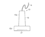
図2に示されるように、超音波プローブ13は筐体16を有する。筐体16内には超音波トランスデューサー素子ユニット(以下「素子ユニット」という)17が収容される。素子ユニット17の表面は筐体16の表面で露出することができる。素子ユニット17は表面から超音波を出力するとともに超音波の反射波を受信する。その他、超音波プローブ13は、プローブ本体13aに着脱自在に連結されるプローブヘッド13bを備えることができる。このとき、素子ユニット17はプローブヘッド13bの筐体16内に組み込まれることができる。
As shown in FIG. 2, the
図3は一実施形態に係る素子ユニット17の平面図を概略的に示す。素子ユニット17は基体21を備える。基体21には素子アレイ22が形成される。素子アレイ22は超音波トランスデューサー素子(以下「素子」という)23の配列で構成される。配列は複数行複数列のマトリクスで形成される。その他、配列では千鳥配置が確立されてもよい。千鳥配置では偶数列の素子23群は奇数列の素子23群に対して行ピッチの2分の1でずらされればよい。奇数列および偶数列の一方の素子数は他方の素子数に比べて1つ少なくてもよい。
FIG. 3 schematically shows a plan view of the
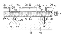
個々の素子23は振動膜(振動板)24を備える。振動膜24の詳細は後述される。図3では振動膜24の膜面に直交する方向の平面視(基板の厚み方向からの平面視)で振動膜24の輪郭が点線で描かれる。輪郭の内側は振動膜24の領域内に相当する。輪郭の外側は振動膜24の領域外に相当する。振動膜24上には圧電素子25が形成される。圧電素子25では、後述されるように、上電極(第2電極膜)26および下電極(第1電極膜)27の間に圧電体膜(図示されず)が挟まれる。これらは順番に重ねられる。素子ユニット17は1枚の超音波トランスデューサー素子チップとして構成される。
Each
基体21の表面には複数本の第1導電体28が形成される。第1導電体28は配列の列方向に相互に平行に延びる。1列の素子23ごとに1本の第1導電体28が割り当てられる。1本の第1導電体28は配列の列方向に並ぶ素子23に共通に配置される。第1導電体28は個々の素子23ごとに下電極27を形成する。このように第1導電体28は振動膜24の領域内および領域外に配置される。第1導電体28には例えばチタン(Ti)、イリジウム(Ir)、白金(Pt)およびチタン(Ti)の積層膜が用いられることができる。ただし、第1導電体28にはその他の導電材が利用されてもよい。
A plurality of
基体21の表面には複数本の第2導電体31が形成される。第2導電体31は配列の行方向に相互に平行に延びる。1行の素子23ごとに1本の第2導電体31が割り当てられる。1本の第2導電体31は配列の行方向に並ぶ素子23に共通に接続される。第2導電体31は個々の素子23ごとに上電極26を形成する。第2導電体31の両端は1対の引き出し配線32にそれぞれ接続される。引き出し配線32は配列の列方向に相互に平行に延びる。したがって、全ての第2導電体31は同一長さを有する。こうしてマトリクス全体の素子23に共通に上電極26は接続される。このように第2導電体31は振動膜24の領域内および領域外に配置される。第2導電体31は例えばイリジウム(Ir)で形成されることができる。ただし、第2導電体31にはその他の導電材が利用されてもよい。
A plurality of
列ごとに素子23の通電は切り替えられる。こうした通電の切り替えに応じてリニアスキャンやセクタースキャンは実現される。1列の素子23は同時に超音波を出力することから、1列の個数すなわち配列の行数は超音波の出力レベルに応じて決定されることができる。行数は例えば10〜15行程度に設定されればよい。図中では省略されて5行が描かれる。配列の列数はスキャンの範囲の広がりに応じて決定されることができる。列数は例えば128列や256列に設定されればよい。図中では省略されて8列が描かれる。上電極26および下電極27の役割は入れ替えられてもよい。すなわち、マトリクス全体の素子23に共通に下電極が接続される一方で、配列の列ごとに共通に上電極が接続されてもよい。
Energization of the
基体21の輪郭は、相互に平行な1対の直線で仕切られて対向する第1辺21aおよび第2辺21bを有する。第1辺21aと素子アレイ22の輪郭との間に1ラインの第1端子アレイ33aが配置される。第2辺21bと素子アレイ22の輪郭との間に1ラインの第2端子アレイ33bが配置される。第1端子アレイ33aは第1辺21aに平行に1ラインを形成することができる。第2端子アレイ33bは第2辺21bに平行に1ラインを形成することができる。第1端子アレイ33aは1対の上電極端子34および複数の下電極端子35で構成される。同様に、第2端子アレイ33bは1対の上電極端子36および複数の下電極端子37で構成される。1本の引き出し配線32の両端にそれぞれ上電極端子34、36は接続される。引き出し配線32および上電極端子34、36は素子アレイ22を二等分する垂直面で面対称に形成されればよい。1本の第2導電体31の両端にそれぞれ下電極端子35、37は接続される。第2導電体31および下電極端子35、37は素子アレイ22を二等分する垂直面で面対称に形成されればよい。ここでは、基体21の輪郭は矩形に形成される。基体21の輪郭は正方形であってもよく台形であってもよい。
The outline of the
基体21には第1フレキシブルプリント配線板(以下「第1配線板」という)38が連結される。第1配線板38は第1端子アレイ33aに覆い被さる。第1配線板38の一端には上電極端子34および下電極端子35に個別に対応して導電線すなわち第1信号線39が形成される。第1信号線39は上電極端子34および下電極端子35に個別に向き合わせられ個別に接合される。同様に、基体21には第2フレキシブルプリント配線板(以下「第2配線板」という)41が覆い被さる。第2配線板41は第2端子アレイ33bに覆い被さる。第2配線板41の一端には上電極端子36および下電極端子37に個別に対応して導電線すなわち第2信号線42が形成される。第2信号線42は上電極端子36および下電極端子37に個別に向き合わせられ個別に接合される。
A first flexible printed wiring board (hereinafter referred to as “first wiring board”) 38 is connected to the
振動膜24上では第2導電体31に並列に電極分離膜43が配置される。電極分離膜43は第2導電体31の長手方向に帯状に延びる。電極分離膜43は絶縁性および防湿性を有する。電極分離膜43は例えばアルミナ(Al2O3)や酸化シリコン(SiO2)といった防湿性絶縁材から形成される。電極分離膜43は個々の第2導電体31を挟んで第2導電体31の両側に分離して形成される。第2導電体31は振動膜24上で第1導電体28に交差することから、電極分離膜43は振動膜24上で第1導電体28上を横切る。
An
基体21上で振動膜24の領域外には絶縁膜44が形成される。絶縁膜44は第1導電体28の長手方向に帯状に延びる。絶縁膜44は第1導電体28に並列に配置される。絶縁膜44は例えばアルミナや酸化シリコンといった防湿性の絶縁材から形成される。絶縁膜44の素材は電極分離膜43の素材と一致すればよい。絶縁膜44は第2導電体31上を横切る。こうして絶縁膜44は第2導電体31上に形成される。絶縁膜44は電極分離膜43に連続する。絶縁膜44は、第2導電体31を挟んで第2導電体31の両側に配置される電極分離膜43に接続される。
An insulating
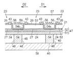
図4に示されるように、基体21は基板46および可撓膜47を備える。基板46の表面に可撓膜47が一面に形成される。基板46には個々の素子23ごとに開口48が形成される。開口48は基板46に対してアレイ状に配置される。開口48が配置される領域の輪郭は素子アレイ22の輪郭に相当する。隣接する2つの開口48の間には仕切り壁49が区画される。隣接する開口48は仕切り壁49で仕切られる。仕切り壁49の壁厚みは開口48の間隔に相当する。仕切り壁49は相互に平行に広がる平面内に2つの壁面を規定する。壁厚みは2つの壁面の距離に相当する。すなわち、壁厚みは壁面に直交して壁面の間に挟まれる垂線の長さで規定されることができる。
As shown in FIG. 4, the
可撓膜47は、基板46の表面に積層される酸化シリコン(SiO2)層51と、酸化シリコン層51の表面に積層される酸化ジルコニウム(ZrO2)層52とで構成される。可撓膜47は開口48に接する。こうして開口48の輪郭に対応して可撓膜47の一部が振動膜24を形成する。振動膜24は、可撓膜47のうち、開口48に臨むことから基板46の厚み方向に膜振動することができる部分である。酸化シリコン層51の膜厚は共振周波数に基づき決定されることができる。
The
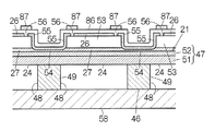
振動膜24の表面に下電極27、圧電体膜53および上電極26が順番に積層される。圧電体膜53は例えばジルコン酸チタン酸鉛(PZT)で形成されることができる。圧電体膜53にはその他の圧電材料が用いられてもよい。ここで、第1導電体28は下電極27および第1導電膜54を有する。第1導電膜54は下電極27に接続される。第1導電膜54は下電極27に連続する。第1導電膜54の膜厚は下電極27の膜厚よりも大きい。第1導電膜54には第2導電膜55が接続される。第2導電膜55は、第1導電膜54から分岐し圧電体膜53上に延び、上電極26から離隔した位置で途切れる。1つの下電極27に関し、第1導電膜54は、基体21の厚み方向からの平面視で下電極27と振動膜24の第1方向D1の端部(以下「第1方向端部」という)との間に形成される第1方向導電体部54aと、下電極27と第1方向端部とは下電極27と挟んで反対側の第2方向D2の端部(以下「第2方向端部」という)との間に形成される第2方向導電体部54bとを有する。第2導電膜55は、第1方向導電体部54aに接続されて、圧電体膜53上で上電極26から離隔される第1上層導電体部55aと、第2方向導電体部54bに接続されて、圧電体膜53上で上電極26から離隔される第2上層導電体部55bとを有する。圧電体膜53の頂上面には、上電極26と第1上層導電体部55aとの間に隙間56が形成され、上電極26と第2上層導電体部55bとの間に隙間56が形成される。
A
図4に示されるように、上電極26と第1上層導電体部55aとの間に電極分離膜43は形成される。同様に、上電極26と第2上層導電体部55bとの間に電極分離膜43は形成される。電極分離膜43は圧電体膜53の頂上面で隙間56を塞ぐ。電極分離膜43は隙間56に充填される。こうして上電極26および第2導電膜55の間で圧電体膜53の表面は電極分離膜43で覆われる。ここでは、第1導電体28の長手方向に電極分離膜43は振動膜24の領域内に留まる。電極分離膜43は振動膜24の縁に係らない。
As shown in FIG. 4, the
基体21の表面には保護膜57が積層される。保護膜57は例えば全面にわたって基体21の表面に覆い被さる。その結果、素子アレイ22や第1および第2端子アレイ33a、33b、第1および第2配線板38、41は保護膜57で覆われる。保護膜57には例えばシリコーン樹脂膜が用いられることができる。保護膜57は、素子アレイ22の構造や、第1端子アレイ33aおよび第1配線板38の接合、第2端子アレイ33bおよび第2配線板41の接合を保護する。
A
基体21の裏面には補強板58が固定される。補強板58の表面に基体21の裏面が重ねられる。補強板58は素子ユニット17の裏面で開口48を閉じる。補強板58はリジッドな基材を備えることができる。補強板58は例えばシリコン基板から形成されることができる。基体21の板厚は例えば100μm程度に設定され、補強板58の板厚は例えば100〜150μm程度に設定される。ここでは、仕切り壁49は補強板58に結合される。補強板58は個々の仕切り壁49に少なくとも1カ所の接合域で接合される。接合にあたって接着剤は用いられることができる。
A reinforcing
(2)超音波診断装置の回路構成
図5に示されるように、超音波診断装置11は素子ユニット17に電気的に接続される集積回路チップ59を備える。集積回路チップ59はマルチプレクサー60および送受信回路61を備える。マルチプレクサー60は素子ユニット17側のポート群60aと送受信回路61側のポート群60bとを備える。素子ユニット17側のポート群60aには配線62経由で第1信号線38および第2信号線42が接続される。こうしてポート群60aは素子アレイ22に繋がる。ここでは、送受信回路61側のポート群60bには集積回路チップ55内の規定数の信号線63が接続される。規定数はスキャンにあたって同時に出力される素子23の列数に相当する。マルチプレクサー60はケーブル14側のポートと素子ユニット17側のポートとの間で相互接続を管理する。
(2) Circuit Configuration of Ultrasonic Diagnostic Device As shown in FIG. 5, the ultrasonic
送受信回路61は規定数の切り替えスイッチ64を備える。個々の切り替えスイッチ64はそれぞれ個別に対応の信号線63に接続される。送受信回路61は個々の切り替えスイッチ64ごとに送信経路65および受信経路66を備える。切り替えスイッチ64には送信経路65と受信経路66とが並列に接続される。切り替えスイッチ64はマルチプレクサー60に選択的に送信経路65または受信経路66を接続する。送信経路65にはパルサー67が組み込まれる。パルサー67は振動膜52の共振周波数に応じた周波数でパルス信号を出力する。受信経路66にはアンプ68、ローパスフィルター(LPF)69およびアナログデジタル変換器(ADC)71が組み込まれる。個々の素子23の出力信号は増幅されてデジタル信号に変換される。
The transmission /
送受信回路61は駆動/受信回路72を備える。送信経路65および受信経路66は駆動/受信回路72に接続される。駆動/受信回路72はスキャンの形態に応じて同時にパルサー67を制御する。駆動/受信回路72はスキャンの形態に応じて出力信号のデジタル信号を受信する。駆動/受信回路72は制御線73でマルチプレクサー60に接続される。マルチプレクサー60は駆動/受信回路72から供給される制御信号に基づき相互接続の管理を実施する。
The transmission /
装置端末12には処理回路(処理部)74が組み込まれる。処理回路74は例えば中央演算処理装置(CPU)やメモリーを備えることができる。超音波診断装置11の全体動作は処理回路74の処理に従って制御される。ユーザーから入力される指示に応じて処理回路74は駆動/受信回路72を制御する。処理回路74は素子23の出力信号に応じて画像を生成する。画像は描画データで特定される。
A processing circuit (processing unit) 74 is incorporated in the
装置端末12には描画回路75が組み込まれる。描画回路75は処理回路74に接続される。描画回路75にはディスプレイパネル15が接続される。描画回路75は処理回路74で生成された描画データに応じて駆動信号を生成する。駆動信号はディスプレイパネル15に送り込まれる。その結果、ディスプレイパネル15に画像が映し出される。
A
(3)超音波診断装置の動作
次に超音波診断装置11の動作を簡単に説明する。処理回路74は駆動/受信回路72に超音波の送信および受信を指示する。駆動/受信回路72はマルチプレクサー60に制御信号を供給するとともに個々のパルサー67に駆動信号を供給する。パルサー67は駆動信号の供給に応じてパルス信号を出力する。マルチプレクサー60は制御信号の指示に従ってポート群60bのポートにポート群60aのポートを接続する。パルス信号はポートの選択に応じて上電極端子34、36および下電極端子35、37を通じて列ごとに素子23に供給される。パルス信号の供給に応じて振動膜24は振動する。その結果、対象物(例えば人体の内部)に向けて所望の超音波ビームは発せられる。
(3) Operation of Ultrasonic Diagnostic Device Next, the operation of the ultrasonic
超音波の送信後、切り替えスイッチ64は切り替えられる。マルチプレクサー60はポートの接続関係を維持する。切り替えスイッチ64は送信経路65および信号線63の接続に代えて受信経路66および信号線63の接続を確立する。超音波の反射波は振動膜24を振動させる。その結果、素子23から出力信号が出力される。出力信号はデジタル信号に変換されて駆動/受信回路72に送り込まれる。
After transmission of the ultrasonic wave, the
超音波の送信および受信は繰り返される。繰り返しにあたってマルチプレクサー60はポートの接続関係を変更する。その結果、リニアスキャンやセクタースキャンは実現される。スキャンが完了すると、処理回路74は出力信号のデジタル信号に基づき画像を形成する。形成された画像はディスプレイパネル15の画面に表示される。
Transmission and reception of ultrasonic waves are repeated. In the repetition, the
振動膜24には超音波が作用する。超音波は振動膜24の超音波振動を引き起こす。振動膜24の超音波振動に応じて圧電素子25から電流が出力される。こうして個々の素子23は超音波を検出する。ここで、第1導電膜54は下電極27の配線膜として機能する。第1導電膜54には十分な膜厚が確保されることができる。配線抵抗の増加は回避されることができる。したがって、超音波の検出感度は十分に確保されることができる。
Ultrasonic waves act on the
前述のように、第2導電膜55は上電極26から離間されることから、第2導電膜55と上電極26との間には隙間56が形成される。電極分離膜43は隙間56に対する湿気の浸入を阻止する。その結果、素子ユニット17が湿気に曝されても、上電極26と第2導電膜55との間で電気的短絡は回避されることができる。しかも、電極分離膜43は振動膜24の縁に係らないことから、振動膜24の可撓性は良好に維持される。したがって、超音波の検出感度は維持されることができる。
As described above, since the second
上電極26の膜厚と第2導電膜55の膜厚とは等しい。したがって、上電極26および第2導電膜55は1層の導電膜から形成されることができる。後述されるように、上電極26および第2導電膜55は共通の製造工程で形成されることができる。製造工程は簡素化されることができる。
The film thickness of the
絶縁膜44は、第2導電体31を挟んで第2導電体31の両側に配置される2つの電極分離膜43が相互に離れる方向に変位することを規制することから、電極分離膜43の接合強度は高められることができる。加えて、絶縁膜44は基体21の表面に形成されることから、絶縁膜44の接合強度は高められることができる。その結果、電極分離膜43の接合強度は高められる。
The insulating
(4)素子ユニットの製造方法
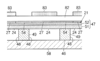
次に素子ユニット17の製造方法を簡単に説明する。図6に示されるように、基体21が用意される。基体21ではアレイ状に振動膜24が配置される。基体21の表面に一面に第1素材膜81が形成される。第1素材膜81は均一な膜厚を有する。第1素材膜81は導電材から形成される。第1素材膜81は振動膜24の表面に被さる。
(4) Method for Manufacturing Element Unit Next, a method for manufacturing the
第1素材膜81から下電極27および第1導電膜54が形成される。形成にあたってフォトリソグラフィ技術が用いられればよい。下電極27および第1導電膜54は基体21の表面で連続する。この時点では下電極27の膜厚と第1導電膜54の膜厚とは一致する。
The
続いて振動膜24上では圧電体膜53が形成される。圧電体膜53の形成にあたって、図7に示されるように、基体21の表面に一面に第2素材膜82が形成される。第2素材膜82は均一な膜厚を有する。第2素材膜82は圧電体材料から形成される。第2素材膜82上には所定のパターンに従ってレジスト膜83が形成される。レジスト膜83の形成にあたって例えばフォトレジスト技術が用いられればよい。レジスト膜83は圧電体膜53の形状を象る。
Subsequently, a
図8に示されるように、第2素材膜82には所定のパターンに従ってエッチング処理が施される。レジスト膜83から外れた位置で第2素材膜82は除去されていく。こうして圧電体膜53は第2素材膜82から形成される。このとき、レジスト膜83から外れた位置で第1導電膜54は表面から削られる。第1導電膜54の膜厚は減少する。こうして第1導電膜54の膜厚は下電極27の膜厚よりも小さくなる。エッチング処理が終了すると、レジスト膜83は除去される。
As shown in FIG. 8, the
続いて振動膜24上では上電極26が形成される。上電極26の形成にあたって、図9に示されるように、基体21の表面に一面に第3素材膜84が形成される。第3素材膜84は均一な膜厚を有する。第3素材膜84は導電材料から形成される。こうして第3素材膜84は少なくとも第1導電膜54および圧電体膜53の露出面に被さる。第1導電膜54の膜厚は増大する。第3素材膜84上には所定のパターンに従ってレジスト膜85が形成される。レジスト膜85の形成にあたって例えばフォトレジスト技術が用いられればよい。レジスト膜85は上電極27および第2導電膜55の形状を象る。
Subsequently, the
図10に示されるように、第3素材膜84には所定のパターンに従ってエッチング処理が施される。レジスト膜85から外れた位置で第3素材膜84は除去されていく。こうして上電極26および第2導電膜55は第3素材膜84から形成される。圧電体膜53上で上電極26の輪郭は仕切られる。圧電体膜53上では、上電極26から隔てられて第2導電膜55が形成される。こうして第3素材膜84には隙間56が形成される。隙間56で第2導電膜55は上電極26から分離される。エッチング処理が終了すると、レジスト膜85は除去される。
As shown in FIG. 10, the
続いて振動膜24上では電極分離膜43が形成される。電極分離膜43の形成にあたって、図11に示されるように、基体21の表面に一面に第4素材膜86が形成される。第4素材膜86は均一な膜厚を有する。第4素材膜86は絶縁材料から形成される。絶縁材料は防湿性を有する。第4素材膜86は少なくとも隙間56に充填される。第4素材膜86上には所定のパターンに従ってレジスト膜87が形成される。レジスト膜87の形成にあたって例えばフォトレジスト技術が用いられればよい。レジスト膜87は電極分離膜43の形状を象る。
Subsequently, an
第4素材膜86には所定のパターンに従ってエッチング処理が施される。レジスト膜87から外れた位置で第4素材膜86は除去されていく。こうして電極分離膜43は第4素材膜86から形成される。エッチング処理が終了すると、レジスト膜87は除去される。その後、基体21の表面には保護膜57が形成される。こうして素子ユニット17は製造される。
The
本実施形態に係る製造方法によれば、圧電体膜53の形成にあたってエッチング処理が施される。このとき、圧電体膜53の周囲では第1導電膜54がエッチング処理に曝される。その結果、第1導電膜54の膜厚は下電極27に比べて減少する。その後、第1導電膜54には第3素材膜84が積層される。こうして第1導電膜54の膜厚は増加する。下電極27に接続される配線膜には十分な膜厚が確保されることができる。配線抵抗の増加は回避されることができる。したがって、超音波の検出感度は十分に確保されることができる。
According to the manufacturing method according to the present embodiment, the etching process is performed when the
なお、上記のように本実施形態について詳細に説明したが、本発明の新規事項および効果から実体的に逸脱しない多くの変形が可能であることは当業者には容易に理解できるであろう。したがって、このような変形例はすべて本発明の範囲に含まれる。例えば、明細書または図面において、少なくとも一度、より広義または同義な異なる用語とともに記載された用語は、明細書または図面のいかなる箇所においても、その異なる用語に置き換えられることができる。また、超音波診断装置11、超音波プローブ13、プローブヘッド13b、素子ユニット17、素子23等の構成および動作も本実施形態で説明したものに限定されず、種々の変形が可能である。
Although the present embodiment has been described in detail as described above, it will be easily understood by those skilled in the art that many modifications can be made without departing from the novel matters and effects of the present invention. Therefore, all such modifications are included in the scope of the present invention. For example, a term described with a different term having a broader meaning or the same meaning at least once in the specification or the drawings can be replaced with the different term in any part of the specification or the drawings. Further, the configurations and operations of the ultrasonic
11 電子機器および超音波画像装置としての超音波診断装置、13 プローブ(超音波プローブ)、15 表示装置(ディスプレイパネル)、16 筐体、17 超音波トランスデューサー装置の一部を構成する超音波トランスデューサー素子ユニット、21 基体、24 子dの得板(振動膜)、26 第2電極膜(上電極)、27 第1電極膜(下電極)、43 (第1および第2)絶縁膜(電極分離膜)、53 圧電体膜、54 第1導電膜、54a 第1方向導電体部、54b 第2方向導電体部、55 第2導電膜、55a 第1上層導電体部、55b 第2上層導電体部、74 処理部(処理回路)、81 第1素材膜、82 第2素材膜、84 第3素材膜、D1 第1方向、D2 第2方向。
DESCRIPTION OF
Claims (5)
前記振動膜上に形成される第1電極膜と、
前記第1電極膜上に形成される圧電体膜と、
前記圧電体膜上に形成される第2電極膜と、
前記第1電極膜の膜厚よりも大きい膜厚で形成されて前記第1電極膜に接続される第1導電膜と、
前記第2電極膜から離隔され、かつ、前記第1導電膜に接続されて前記圧電体膜の少なくとも一部を覆うように形成される第2導電膜と、
を備え、
前記第1導電膜は、前記基体の厚み方向からの平面視で前記第1電極膜と前記振動膜の第1方向端部との間に形成される第1方向導電体部と、前記第1電極膜と前記振動膜の前記第1方向端部とは前記第1電極膜を挟んで反対側の第2方向端部との間に形成される第2方向導電体部とを有し、
前記第2導電膜は、前記第1方向導電体部に接続されて前記圧電体膜上で前記第2電極膜から離隔される第1上層導電体部と、前記第2方向導電体部に接続されて前記圧電体膜上で前記第2電極膜から離隔される第2上層導電体部とを有し、
前記圧電体膜上で前記第2電極膜と前記第1上層導電体部との間に第1絶縁膜が形成され、前記圧電体膜上で前記第2電極膜と前記第2上層導電体部との間に第2絶縁膜が形成され、前記第1絶縁膜と第2絶縁膜とは前記第2電極膜上で離隔していることを特徴とする超音波トランスデューサー装置。 A substrate on which a vibrating membrane is disposed;
A first electrode film formed on the vibration film;
A piezoelectric film formed on the first electrode film;
A second electrode film formed on the piezoelectric film;
A first conductive film formed with a film thickness larger than the film thickness of the first electrode film and connected to the first electrode film;
A second conductive film that is spaced apart from the second electrode film and connected to the first conductive film so as to cover at least a part of the piezoelectric film;
With
The first conductive film includes a first direction conductor formed between the first electrode film and a first direction end of the vibration film in a plan view from the thickness direction of the base, and the first The electrode film and the first direction end portion of the vibration film have a second direction conductor portion formed between the second direction end portion on the opposite side across the first electrode film,
The second conductive film is connected to the first directional conductor portion and connected to the first directional conductor portion on the piezoelectric film and separated from the second electrode film on the piezoelectric film. And a second upper layer conductor portion separated from the second electrode film on the piezoelectric film,
A first insulating film is formed on the piezoelectric film between the second electrode film and the first upper conductor part, and the second electrode film and the second upper conductor part are formed on the piezoelectric film. The ultrasonic transducer device is characterized in that a second insulating film is formed between the first and second insulating films, and the first insulating film and the second insulating film are separated from each other on the second electrode film.
前記第1素材膜から、第1電極膜、および、前記第1電極膜から連続する第1導電膜を形成する工程と、
圧電体材料を含む第2素材膜を形成し、前記第2素材膜をエッチング処理を含むパターニング処理により前記第1電極膜上に圧電体膜を形成する工程と、
少なくとも前記第1導電膜および前記圧電体膜を覆うように導電材料を含む第3素材膜を形成する工程と、
前記第3素材膜をエッチング処理を含むパターニング処理により、前記圧電体膜上に第2電極膜を形成し、かつ前記圧電体膜上で前記第2電極膜と離隔し前記第1導電膜に接続する第2導電膜を形成する工程と、
を備えることを特徴とする超音波トランスデューサー装置の製造方法。
Forming a first material film containing a conductive material on a vibration film disposed on a substrate;
Forming a first electrode film and a first conductive film continuous from the first electrode film from the first material film;
Forming a second material film containing a piezoelectric material, and forming the piezoelectric material film on the first electrode film by a patterning process including an etching process on the second material film;
Forming a third material film containing a conductive material so as to cover at least the first conductive film and the piezoelectric film;
A second electrode film is formed on the piezoelectric film by a patterning process including an etching process on the third material film, and is separated from the second electrode film on the piezoelectric film and connected to the first conductive film. Forming a second conductive film to be formed;
A method of manufacturing an ultrasonic transducer device comprising:
Priority Applications (7)
| Application Number | Priority Date | Filing Date | Title |
|---|---|---|---|
| JP2013071582A JP6136464B2 (en) | 2013-03-29 | 2013-03-29 | ULTRASONIC TRANSDUCER DEVICE AND PROBE, ELECTRONIC DEVICE, AND ULTRASONIC IMAGING DEVICE |
| TW103111139A TWI632710B (en) | 2013-03-29 | 2014-03-25 | Ultrasonic transducer device, ultrasonic probe, electronic instrument, and ultrasonic diagnostic device |
| KR1020140035299A KR102106653B1 (en) | 2013-03-29 | 2014-03-26 | Ultrasonic transducer device, probe, electronic instrument, and ultrasonic image device |
| CN201410120672.6A CN104068893B (en) | 2013-03-29 | 2014-03-27 | Ultrasound transducer apparatus and its manufacturing method, detector, electronic equipment |
| US14/227,558 US9592031B2 (en) | 2013-03-29 | 2014-03-27 | Ultrasonic transducer device, probe, electronic instrument, and ultrasonic diagnostic device |
| EP14162330.6A EP2783759A3 (en) | 2013-03-29 | 2014-03-28 | Ultrasonic transducer device, probe, electronic instrument, and ultrasonic diagnostic device |
| US15/417,875 US9782150B2 (en) | 2013-03-29 | 2017-01-27 | Ultrasonic transducer device, probe, electronic instrument, and ultrasonic diagnostic device |
Applications Claiming Priority (1)
| Application Number | Priority Date | Filing Date | Title |
|---|---|---|---|
| JP2013071582A JP6136464B2 (en) | 2013-03-29 | 2013-03-29 | ULTRASONIC TRANSDUCER DEVICE AND PROBE, ELECTRONIC DEVICE, AND ULTRASONIC IMAGING DEVICE |
Related Child Applications (1)
| Application Number | Title | Priority Date | Filing Date |
|---|---|---|---|
| JP2017089381A Division JP6365726B2 (en) | 2017-04-28 | 2017-04-28 | Ultrasonic transducer device and electronic equipment |
Publications (3)
| Publication Number | Publication Date |
|---|---|
| JP2014195494A JP2014195494A (en) | 2014-10-16 |
| JP2014195494A5 JP2014195494A5 (en) | 2016-03-24 |
| JP6136464B2 true JP6136464B2 (en) | 2017-05-31 |
Family
ID=50389918
Family Applications (1)
| Application Number | Title | Priority Date | Filing Date |
|---|---|---|---|
| JP2013071582A Active JP6136464B2 (en) | 2013-03-29 | 2013-03-29 | ULTRASONIC TRANSDUCER DEVICE AND PROBE, ELECTRONIC DEVICE, AND ULTRASONIC IMAGING DEVICE |
Country Status (6)
| Country | Link |
|---|---|
| US (2) | US9592031B2 (en) |
| EP (1) | EP2783759A3 (en) |
| JP (1) | JP6136464B2 (en) |
| KR (1) | KR102106653B1 (en) |
| CN (1) | CN104068893B (en) |
| TW (1) | TWI632710B (en) |
Families Citing this family (8)
| Publication number | Priority date | Publication date | Assignee | Title |
|---|---|---|---|---|
| WO2016121765A1 (en) * | 2015-01-29 | 2016-08-04 | 富士フイルム株式会社 | Electroacoustic conversion film and method for manufacturing electroacoustic conversion film |
| JP6809094B2 (en) | 2016-09-29 | 2021-01-06 | セイコーエプソン株式会社 | Piezoelectric elements, piezoelectric actuators, ultrasonic probes, ultrasonic devices, electronic devices, liquid injection heads, and liquid injection devices |
| JP6862820B2 (en) | 2016-12-26 | 2021-04-21 | セイコーエプソン株式会社 | Ultrasonic devices and ultrasonic devices |
| JP6891506B2 (en) | 2017-01-17 | 2021-06-18 | セイコーエプソン株式会社 | Piezoelectric elements, piezoelectric actuators, ultrasonic probes, ultrasonic devices, electronic devices, liquid injection heads, and liquid injection devices |
| JP2018157125A (en) | 2017-03-21 | 2018-10-04 | セイコーエプソン株式会社 | Piezoelectric element, ultrasonic sensor, discharge head, ultrasonic device, liquid discharge device and manufacturing method of piezoelectric element |
| JP7047253B2 (en) * | 2017-03-22 | 2022-04-05 | セイコーエプソン株式会社 | Ultrasonic device unit, ultrasonic probe, and ultrasonic device |
| JP2018164039A (en) | 2017-03-27 | 2018-10-18 | セイコーエプソン株式会社 | Piezoelectric element, piezoelectric device, ultrasonic probe, and electronic apparatus |
| JP6874463B2 (en) * | 2017-03-27 | 2021-05-19 | セイコーエプソン株式会社 | Piezoelectric elements, piezoelectric actuators, ultrasonic probes, ultrasonic devices, electronic devices, liquid injection heads, and liquid injection devices |
Family Cites Families (18)
| Publication number | Priority date | Publication date | Assignee | Title |
|---|---|---|---|---|
| JPS61144565A (en) * | 1984-12-18 | 1986-07-02 | Toshiba Corp | High-polymer piezo-electric type ultrasonic probe |
| JP2745147B2 (en) | 1989-03-27 | 1998-04-28 | 三菱マテリアル 株式会社 | Piezoelectric transducer |
| JPH0835954A (en) | 1994-07-22 | 1996-02-06 | Hitachi Constr Mach Co Ltd | Ultrasonic probe |
| JPH0888899A (en) | 1994-09-19 | 1996-04-02 | Daishinku Co | Ultrasonic vibrator |
| DE69714909T2 (en) * | 1996-05-27 | 2003-04-30 | Ngk Insulators Ltd | Piezoelectric element of the thin film type |
| JP2001291907A (en) | 2000-04-06 | 2001-10-19 | Matsushita Electric Ind Co Ltd | Flexible piezoelectric element |
| JP2005051688A (en) | 2003-07-31 | 2005-02-24 | Matsushita Electric Works Ltd | Ultrasonic array sensor and manufacturing method thereof |
| EP1671794A4 (en) | 2003-09-24 | 2009-04-08 | Seiko Epson Corp | Liquid injection head and method of producing the same and liquid injection device |
| JP4744849B2 (en) * | 2004-11-11 | 2011-08-10 | 株式会社東芝 | Semiconductor device |
| JP4614068B2 (en) | 2005-01-24 | 2011-01-19 | セイコーエプソン株式会社 | Liquid ejecting head, manufacturing method thereof, and liquid ejecting apparatus |
| JP2006231909A (en) | 2005-01-26 | 2006-09-07 | Seiko Epson Corp | Liquid jetting head and liquid jetting apparatus |
| JP4844717B2 (en) | 2005-12-27 | 2011-12-28 | セイコーエプソン株式会社 | Method for manufacturing liquid jet head |
| WO2007091311A1 (en) * | 2006-02-08 | 2007-08-16 | Tohoku Pioneer Corporation | Method of manufacturing display having saw touch sensor |
| US8508103B2 (en) * | 2009-03-23 | 2013-08-13 | Sonavation, Inc. | Piezoelectric identification device and applications thereof |
| WO2010148398A2 (en) * | 2009-06-19 | 2010-12-23 | The Regents Of The University Of Michigan | A thin-film device and method of fabricating the same |
| JP5671876B2 (en) * | 2009-11-16 | 2015-02-18 | セイコーエプソン株式会社 | Ultrasonic transducer, ultrasonic sensor, method for manufacturing ultrasonic transducer, and method for manufacturing ultrasonic sensor |
| JP5754129B2 (en) * | 2010-03-11 | 2015-07-29 | セイコーエプソン株式会社 | Piezoelectric element, piezoelectric sensor, electronic device, and method of manufacturing piezoelectric element |
| JP5708364B2 (en) * | 2011-08-22 | 2015-04-30 | セイコーエプソン株式会社 | Ultrasonic array sensor and manufacturing method thereof |
-
2013
- 2013-03-29 JP JP2013071582A patent/JP6136464B2/en active Active
-
2014
- 2014-03-25 TW TW103111139A patent/TWI632710B/en active
- 2014-03-26 KR KR1020140035299A patent/KR102106653B1/en active IP Right Grant
- 2014-03-27 CN CN201410120672.6A patent/CN104068893B/en active Active
- 2014-03-27 US US14/227,558 patent/US9592031B2/en active Active
- 2014-03-28 EP EP14162330.6A patent/EP2783759A3/en not_active Withdrawn
-
2017
- 2017-01-27 US US15/417,875 patent/US9782150B2/en active Active
Also Published As
| Publication number | Publication date |
|---|---|
| KR20140118856A (en) | 2014-10-08 |
| US20140296716A1 (en) | 2014-10-02 |
| EP2783759A3 (en) | 2015-10-28 |
| CN104068893A (en) | 2014-10-01 |
| JP2014195494A (en) | 2014-10-16 |
| US9782150B2 (en) | 2017-10-10 |
| US20170128047A1 (en) | 2017-05-11 |
| US9592031B2 (en) | 2017-03-14 |
| CN104068893B (en) | 2018-10-19 |
| TW201438477A (en) | 2014-10-01 |
| KR102106653B1 (en) | 2020-05-04 |
| EP2783759A2 (en) | 2014-10-01 |
| TWI632710B (en) | 2018-08-11 |
Similar Documents
| Publication | Publication Date | Title |
|---|---|---|
| JP5990930B2 (en) | Ultrasonic transducer element chip and probe, electronic device and ultrasonic diagnostic apparatus | |
| JP6136464B2 (en) | ULTRASONIC TRANSDUCER DEVICE AND PROBE, ELECTRONIC DEVICE, AND ULTRASONIC IMAGING DEVICE | |
| JP6078994B2 (en) | Ultrasonic transducer element unit, probe, probe head, electronic device, and ultrasonic diagnostic apparatus | |
| JP5990929B2 (en) | Ultrasonic transducer device and probe, electronic device and ultrasonic diagnostic device | |
| JP6089499B2 (en) | Ultrasonic transducer device and probe, electronic device and ultrasonic diagnostic device | |
| JP6102075B2 (en) | Ultrasonic transducer element chip and probe, electronic device and ultrasonic diagnostic apparatus | |
| JP6442821B2 (en) | Ultrasonic device and electronic equipment | |
| JP6252279B2 (en) | ULTRASONIC TRANSDUCER DEVICE AND PROBE, ELECTRONIC DEVICE, AND ULTRASONIC IMAGING DEVICE | |
| JP2015195351A (en) | Piezoelectric element, piezoelectric device and probe, and electronic device and ultrasonic image device | |
| US10042044B2 (en) | Ultrasonic device, probe, electronic device, and ultrasonic imaging apparatus | |
| JP2013211604A (en) | Ultrasonic transducer element chip, probe, electronic apparatus and ultrasonic diagnostic device | |
| JP6273743B2 (en) | Ultrasonic device and probe, electronic apparatus and ultrasonic imaging apparatus | |
| JP2014195495A (en) | Ultrasonic transducer device, probe, electronic device, and ultrasonic image device | |
| JP2015130994A (en) | Ultrasonic device, ultrasonic transducer device, electronic apparatus and ultrasonic imaging device | |
| JP6365726B2 (en) | Ultrasonic transducer device and electronic equipment | |
| JP2017000792A (en) | Ultrasonic transducer element chip, probe, electronic device, and ultrasonic diagnostic device | |
| JP6311815B2 (en) | Ultrasonic transducer element chip and probe, electronic device and ultrasonic diagnostic apparatus | |
| JP6222259B2 (en) | Ultrasonic transducer element chip and probe, electronic device and ultrasonic diagnostic apparatus |
Legal Events
| Date | Code | Title | Description |
|---|---|---|---|
| RD04 | Notification of resignation of power of attorney |
Free format text: JAPANESE INTERMEDIATE CODE: A7424 Effective date: 20150113 |
|
| A521 | Request for written amendment filed |
Free format text: JAPANESE INTERMEDIATE CODE: A523 Effective date: 20160205 |
|
| A621 | Written request for application examination |
Free format text: JAPANESE INTERMEDIATE CODE: A621 Effective date: 20160205 |
|
| RD02 | Notification of acceptance of power of attorney |
Free format text: JAPANESE INTERMEDIATE CODE: A7422 Effective date: 20160205 |
|
| RD03 | Notification of appointment of power of attorney |
Free format text: JAPANESE INTERMEDIATE CODE: A7423 Effective date: 20160205 |
|
| RD04 | Notification of resignation of power of attorney |
Free format text: JAPANESE INTERMEDIATE CODE: A7424 Effective date: 20160610 |
|
| A977 | Report on retrieval |
Free format text: JAPANESE INTERMEDIATE CODE: A971007 Effective date: 20161227 |
|
| A131 | Notification of reasons for refusal |
Free format text: JAPANESE INTERMEDIATE CODE: A131 Effective date: 20170124 |
|
| A521 | Request for written amendment filed |
Free format text: JAPANESE INTERMEDIATE CODE: A523 Effective date: 20170322 |
|
| TRDD | Decision of grant or rejection written | ||
| A01 | Written decision to grant a patent or to grant a registration (utility model) |
Free format text: JAPANESE INTERMEDIATE CODE: A01 Effective date: 20170404 |
|
| A61 | First payment of annual fees (during grant procedure) |
Free format text: JAPANESE INTERMEDIATE CODE: A61 Effective date: 20170417 |
|
| R150 | Certificate of patent or registration of utility model |
Ref document number: 6136464 Country of ref document: JP Free format text: JAPANESE INTERMEDIATE CODE: R150 |