JP5671876B2 - Ultrasonic transducer, ultrasonic sensor, method for manufacturing ultrasonic transducer, and method for manufacturing ultrasonic sensor - Google Patents
Ultrasonic transducer, ultrasonic sensor, method for manufacturing ultrasonic transducer, and method for manufacturing ultrasonic sensor Download PDFInfo
- Publication number
- JP5671876B2 JP5671876B2 JP2010182113A JP2010182113A JP5671876B2 JP 5671876 B2 JP5671876 B2 JP 5671876B2 JP 2010182113 A JP2010182113 A JP 2010182113A JP 2010182113 A JP2010182113 A JP 2010182113A JP 5671876 B2 JP5671876 B2 JP 5671876B2
- Authority
- JP
- Japan
- Prior art keywords
- ultrasonic
- diaphragm
- piezoelectric body
- ultrasonic transducer
- forming
- Prior art date
- Legal status (The legal status is an assumption and is not a legal conclusion. Google has not performed a legal analysis and makes no representation as to the accuracy of the status listed.)
- Active
Links
- 238000000034 method Methods 0.000 title claims description 67
- 238000004519 manufacturing process Methods 0.000 title claims description 61
- 239000000758 substrate Substances 0.000 claims description 130
- 238000004891 communication Methods 0.000 claims description 34
- 238000005530 etching Methods 0.000 claims description 17
- 238000010030 laminating Methods 0.000 claims description 15
- 238000006073 displacement reaction Methods 0.000 claims description 13
- 230000015572 biosynthetic process Effects 0.000 claims description 8
- 239000010408 film Substances 0.000 description 61
- 230000008569 process Effects 0.000 description 50
- 230000005540 biological transmission Effects 0.000 description 36
- 230000002093 peripheral effect Effects 0.000 description 25
- 229910004298 SiO 2 Inorganic materials 0.000 description 21
- 238000005452 bending Methods 0.000 description 17
- 230000008602 contraction Effects 0.000 description 16
- HFGPZNIAWCZYJU-UHFFFAOYSA-N lead zirconate titanate Chemical compound [O-2].[O-2].[O-2].[O-2].[O-2].[Ti+4].[Zr+4].[Pb+2] HFGPZNIAWCZYJU-UHFFFAOYSA-N 0.000 description 15
- 229910052451 lead zirconate titanate Inorganic materials 0.000 description 15
- 239000000463 material Substances 0.000 description 12
- 238000003491 array Methods 0.000 description 10
- 101100123718 Neurospora crassa (strain ATCC 24698 / 74-OR23-1A / CBS 708.71 / DSM 1257 / FGSC 987) pda-1 gene Proteins 0.000 description 9
- 230000004048 modification Effects 0.000 description 8
- 238000012986 modification Methods 0.000 description 8
- 239000011159 matrix material Substances 0.000 description 7
- 238000001020 plasma etching Methods 0.000 description 6
- 239000010409 thin film Substances 0.000 description 6
- 238000001514 detection method Methods 0.000 description 5
- 238000012545 processing Methods 0.000 description 5
- 239000000919 ceramic Substances 0.000 description 4
- 238000010586 diagram Methods 0.000 description 4
- 229910052746 lanthanum Inorganic materials 0.000 description 4
- 238000004544 sputter deposition Methods 0.000 description 4
- 238000004140 cleaning Methods 0.000 description 3
- 238000003475 lamination Methods 0.000 description 3
- 230000000149 penetrating effect Effects 0.000 description 3
- 230000035945 sensitivity Effects 0.000 description 3
- XUIMIQQOPSSXEZ-UHFFFAOYSA-N Silicon Chemical compound [Si] XUIMIQQOPSSXEZ-UHFFFAOYSA-N 0.000 description 2
- RTAQQCXQSZGOHL-UHFFFAOYSA-N Titanium Chemical compound [Ti] RTAQQCXQSZGOHL-UHFFFAOYSA-N 0.000 description 2
- 238000005229 chemical vapour deposition Methods 0.000 description 2
- 230000007423 decrease Effects 0.000 description 2
- NKZSPGSOXYXWQA-UHFFFAOYSA-N dioxido(oxo)titanium;lead(2+) Chemical compound [Pb+2].[O-][Ti]([O-])=O NKZSPGSOXYXWQA-UHFFFAOYSA-N 0.000 description 2
- 238000001312 dry etching Methods 0.000 description 2
- 230000000694 effects Effects 0.000 description 2
- 238000010304 firing Methods 0.000 description 2
- FZLIPJUXYLNCLC-UHFFFAOYSA-N lanthanum atom Chemical compound [La] FZLIPJUXYLNCLC-UHFFFAOYSA-N 0.000 description 2
- 229910052745 lead Inorganic materials 0.000 description 2
- 229910021421 monocrystalline silicon Inorganic materials 0.000 description 2
- 229910052710 silicon Inorganic materials 0.000 description 2
- 239000010703 silicon Substances 0.000 description 2
- 238000007740 vapor deposition Methods 0.000 description 2
- 230000008859 change Effects 0.000 description 1
- 238000000354 decomposition reaction Methods 0.000 description 1
- 230000001066 destructive effect Effects 0.000 description 1
- 230000001939 inductive effect Effects 0.000 description 1
- 238000007689 inspection Methods 0.000 description 1
- 238000005304 joining Methods 0.000 description 1
- 238000003698 laser cutting Methods 0.000 description 1
- 239000004973 liquid crystal related substance Substances 0.000 description 1
- 238000005259 measurement Methods 0.000 description 1
- 230000008018 melting Effects 0.000 description 1
- 238000002844 melting Methods 0.000 description 1
- 239000002184 metal Substances 0.000 description 1
- 229910052751 metal Inorganic materials 0.000 description 1
- 230000003647 oxidation Effects 0.000 description 1
- 238000007254 oxidation reaction Methods 0.000 description 1
- 238000005498 polishing Methods 0.000 description 1
- 238000004151 rapid thermal annealing Methods 0.000 description 1
- 239000004065 semiconductor Substances 0.000 description 1
- 238000009751 slip forming Methods 0.000 description 1
- 239000000126 substance Substances 0.000 description 1
- 238000002604 ultrasonography Methods 0.000 description 1
Images


Classifications
-
- H—ELECTRICITY
- H10—SEMICONDUCTOR DEVICES; ELECTRIC SOLID-STATE DEVICES NOT OTHERWISE PROVIDED FOR
- H10N—ELECTRIC SOLID-STATE DEVICES NOT OTHERWISE PROVIDED FOR
- H10N30/00—Piezoelectric or electrostrictive devices
- H10N30/20—Piezoelectric or electrostrictive devices with electrical input and mechanical output, e.g. functioning as actuators or vibrators
- H10N30/204—Piezoelectric or electrostrictive devices with electrical input and mechanical output, e.g. functioning as actuators or vibrators using bending displacement, e.g. unimorph, bimorph or multimorph cantilever or membrane benders
-
- G—PHYSICS
- G10—MUSICAL INSTRUMENTS; ACOUSTICS
- G10K—SOUND-PRODUCING DEVICES; METHODS OR DEVICES FOR PROTECTING AGAINST, OR FOR DAMPING, NOISE OR OTHER ACOUSTIC WAVES IN GENERAL; ACOUSTICS NOT OTHERWISE PROVIDED FOR
- G10K9/00—Devices in which sound is produced by vibrating a diaphragm or analogous element, e.g. fog horns, vehicle hooters or buzzers
- G10K9/12—Devices in which sound is produced by vibrating a diaphragm or analogous element, e.g. fog horns, vehicle hooters or buzzers electrically operated
- G10K9/122—Devices in which sound is produced by vibrating a diaphragm or analogous element, e.g. fog horns, vehicle hooters or buzzers electrically operated using piezoelectric driving means
-
- H—ELECTRICITY
- H10—SEMICONDUCTOR DEVICES; ELECTRIC SOLID-STATE DEVICES NOT OTHERWISE PROVIDED FOR
- H10N—ELECTRIC SOLID-STATE DEVICES NOT OTHERWISE PROVIDED FOR
- H10N30/00—Piezoelectric or electrostrictive devices
- H10N30/20—Piezoelectric or electrostrictive devices with electrical input and mechanical output, e.g. functioning as actuators or vibrators
- H10N30/204—Piezoelectric or electrostrictive devices with electrical input and mechanical output, e.g. functioning as actuators or vibrators using bending displacement, e.g. unimorph, bimorph or multimorph cantilever or membrane benders
- H10N30/2047—Membrane type
-
- Y—GENERAL TAGGING OF NEW TECHNOLOGICAL DEVELOPMENTS; GENERAL TAGGING OF CROSS-SECTIONAL TECHNOLOGIES SPANNING OVER SEVERAL SECTIONS OF THE IPC; TECHNICAL SUBJECTS COVERED BY FORMER USPC CROSS-REFERENCE ART COLLECTIONS [XRACs] AND DIGESTS
- Y10—TECHNICAL SUBJECTS COVERED BY FORMER USPC
- Y10T—TECHNICAL SUBJECTS COVERED BY FORMER US CLASSIFICATION
- Y10T29/00—Metal working
- Y10T29/42—Piezoelectric device making
Landscapes
- Physics & Mathematics (AREA)
- Engineering & Computer Science (AREA)
- Acoustics & Sound (AREA)
- Multimedia (AREA)
- Transducers For Ultrasonic Waves (AREA)
Description
本発明は、電圧信号を超音波に変換する超音波トランスデューサー、超音波センサー、超音波トランスデューサーの製造方法、および超音波センサーの製造方法に関する。 The present invention relates to an ultrasonic transducer that converts a voltage signal into ultrasonic waves, an ultrasonic sensor, a method for manufacturing an ultrasonic transducer, and a method for manufacturing an ultrasonic sensor.
従来、超音波を出力する超音波トランスデューサーを備えたMEMS(Micro Electro Mechanical Systems)が知られている。このようなMEMSに設けられる超音波トランスデューサーは、極めて小さく形成されるものであるため、超音波の発信源としては、薄膜圧電体が用いられ、この薄膜圧電体の振動によりダイアフラムを変位させることで超音波を出力する構成が一般的である(例えば、特許文献1参照)。
この特許文献1に記載のダイアフラム型超音波センサー素子は、多層膜構造のダイアフラムと、ダイアフラムの一方の面側に形成され、上下電極により挟持されるPZTセラミックス薄膜層と、を備えている。このようなダイアフラム型超音波センサー素子では、上下の電極からPZTセラミックス薄膜層に所定の電圧を印加すると、PZTセラミックス薄膜層が面内方向に対して伸縮し、これに伴ってダイアフラムが面方向に直交する方向に撓んで振動して、超音波が出力される。
Conventionally, MEMS (Micro Electro Mechanical Systems) including an ultrasonic transducer that outputs ultrasonic waves are known. Since the ultrasonic transducer provided in such a MEMS is extremely small, a thin film piezoelectric body is used as an ultrasonic wave transmission source, and the diaphragm is displaced by the vibration of the thin film piezoelectric body. Is generally configured to output ultrasonic waves (see, for example, Patent Document 1).
The diaphragm type ultrasonic sensor element described in
ところで、上記のような特許文献1では、ダイアフラムの振動の振幅は、PZTセラミックス薄膜層の面内方向への伸縮量となり、大きな変位量とはならない。したがって、超音波の音圧が小さいという問題がある。
By the way, in
本発明は、上記のような問題に鑑みて、膜状の圧電体を用いた場合でも、大音圧の超音波を出力可能な超音波トランスデューサー、この超音波トランスデューサーを備えた超音波センサー、超音波トランスデューサーの製造方法、および超音波センサーの製造方法を提供することを目的とする。 In view of the above-described problems, the present invention provides an ultrasonic transducer capable of outputting an ultrasonic wave having a high sound pressure even when a film-like piezoelectric body is used, and an ultrasonic sensor including the ultrasonic transducer. Another object is to provide a method for manufacturing an ultrasonic transducer and a method for manufacturing an ultrasonic sensor.
本発明の超音波トランスデューサーは、開口部を有する支持体と、前記開口部を閉塞するダイアフラムと、前記ダイアフラムに設けられるとともに、電圧の印加により面内方向に伸縮する圧電体と、を備え、前記ダイアフラムは、前記開口部に臨む一面側とは反対側の面に、凹状に形成される凹溝部を備え、前記圧電体は、前記ダイアフラムにおける前記凹溝部の外側に固定されて、前記凹溝部を覆って配置され、前記凹溝部の底面との間に空間を介して対向配置されることを特徴とする。 An ultrasonic transducer of the present invention includes a support having an opening, a diaphragm that closes the opening, and a piezoelectric body that is provided in the diaphragm and expands and contracts in an in-plane direction when a voltage is applied. The diaphragm includes a concave groove portion formed in a concave shape on a surface opposite to the one surface facing the opening, and the piezoelectric body is fixed to the outer side of the concave groove portion in the diaphragm, and the concave groove portion And is disposed opposite to the bottom surface of the concave groove portion through a space.
この発明では、ダイアフラムに凹溝部が形成され、この凹溝部により圧電体とダイアフラムの間に空間が設けられる。そして、この超音波トランスデューサーでは、圧電体に電圧を印加して面内方向に収縮させると、ダイアフラムにおける凹溝部の縁部分の内周壁面が凹溝部の内側方向に変位する。これにより、凹溝部の底面が、ダイアフラムの面方向に対して直交する方向に変位し、振動する。 In the present invention, a concave groove is formed in the diaphragm, and a space is provided between the piezoelectric body and the diaphragm by the concave groove. In this ultrasonic transducer, when a voltage is applied to the piezoelectric body and contracted in the in-plane direction, the inner peripheral wall surface of the edge portion of the concave groove portion of the diaphragm is displaced inward of the concave groove portion. As a result, the bottom surface of the groove portion is displaced in a direction orthogonal to the surface direction of the diaphragm and vibrates.
ここで、ダイアフラム上の圧電体が積層される従来の構成では、ダイアフラムに圧電体の一面側が密着して形成されているため、圧電体に電圧を印加すると、圧電体のダイアフラムに密着されていない他面側のみが収縮し、これによりダイアフラムに反りが生じて撓み、超音波が出力される。この場合、ダイアフラムと圧電素子との密着面が抵抗となるため、圧電素子の収縮量が小さくなり、ダイアフラムの撓み量が小さくなる。また、圧電体の撓み量がそのままダイアフラムの撓み量となり、圧電体の収縮量が小さい場合、ダイアフラムの撓み量も小さくなってしまう。
これに対して、本発明では、ダイアフラムに凹溝部が形成され、圧電体は、この凹溝部の底面と圧電体との間に空間を介在させた状態で凹溝部を覆って設けられている。つまり、圧電体は、凹溝部の底面に対向する領域においてダイアフラムに密着固定されておらず、凹溝部の外周縁において固定されている。このような構成では、凹溝部に対向する領域がダイアフラムに密着されていないため、圧電体が面内方向に対して収縮し、これにより凹溝部の壁部が凹溝部の内側方向に引っ張られ、凹溝部の底面がダイアフラムの面方向に対して直交する方向に撓んで超音波が出力される。この時、圧電体の凹溝部に対向する領域がダイアフラムに密着されていないため、収縮時における抵抗が小さく、圧電体の収縮量も大きくなる。
さらに、本発明では、圧電体の面内方向の収縮量と同寸法だけ、凹溝部の外周縁の内周壁を内側方向に変位させ、これに伴って、凹溝部の底面がダイアフラムの面内方向に対して直交する方向に撓む。このような構成では、ダイアフラムの凹溝部の外周縁自体が凹溝部の内周側に変位するため、凹溝部の底面の変位量も大きくなる。つまり、圧電体の収縮量が小さい場合でも、凹溝部の底面の変位量を大きくすることができる。
したがって、本発明の超音波トランスデューサーでは、例えば従来の圧電量の一面側全体をダイアフラムに密着させる構成に比べて、圧電量の収縮量を大きくでき、圧電量の収縮量に対して凹溝部の底面の変位量も大きくすることができるので、より音圧の大きい大音圧の超音波を出力することができる。
Here, in the conventional configuration in which the piezoelectric bodies on the diaphragm are laminated, since one surface side of the piezoelectric body is in close contact with the diaphragm, when the voltage is applied to the piezoelectric body, the piezoelectric body is not in close contact with the diaphragm. Only the other surface side contracts, whereby the diaphragm warps and bends, and ultrasonic waves are output. In this case, since the contact surface between the diaphragm and the piezoelectric element becomes a resistance, the amount of contraction of the piezoelectric element is reduced, and the amount of deflection of the diaphragm is reduced. Further, the amount of bending of the piezoelectric body becomes the amount of bending of the diaphragm as it is, and when the amount of contraction of the piezoelectric body is small, the amount of bending of the diaphragm is also small.
On the other hand, in the present invention, a groove is formed in the diaphragm, and the piezoelectric body is provided so as to cover the groove with a space interposed between the bottom surface of the groove and the piezoelectric body. That is, the piezoelectric body is not tightly fixed to the diaphragm in the region facing the bottom surface of the groove portion, but is fixed at the outer peripheral edge of the groove portion. In such a configuration, since the region facing the groove portion is not in close contact with the diaphragm, the piezoelectric body contracts in the in-plane direction, whereby the wall portion of the groove portion is pulled inward of the groove portion, Ultrasonic waves are output by bending the bottom surface of the concave groove portion in a direction perpendicular to the surface direction of the diaphragm. At this time, since the region facing the concave groove portion of the piezoelectric body is not in close contact with the diaphragm, the resistance during contraction is small, and the contraction amount of the piezoelectric body is also large.
Furthermore, in the present invention, the inner peripheral wall of the outer peripheral edge of the groove is displaced inward by the same size as the amount of contraction in the in-plane direction of the piezoelectric body, and accordingly, the bottom surface of the groove is in the in-plane direction of the diaphragm. It bends in the direction orthogonal to. In such a configuration, since the outer peripheral edge of the concave groove portion of the diaphragm is displaced toward the inner peripheral side of the concave groove portion, the amount of displacement of the bottom surface of the concave groove portion is also increased. That is, even when the contraction amount of the piezoelectric body is small, the displacement amount of the bottom surface of the groove portion can be increased.
Therefore, in the ultrasonic transducer according to the present invention, for example, the amount of contraction of the piezoelectric amount can be increased as compared with the conventional configuration in which one entire surface of the piezoelectric amount is in close contact with the diaphragm, and the groove portion of the groove portion is smaller than the amount of contraction of the piezoelectric amount. Since the amount of displacement of the bottom surface can be increased, it is possible to output an ultrasonic wave with a higher sound pressure and a higher sound pressure.
本発明の超音波トランスデューサーでは、前記圧電体は、前記凹溝部に対向する位置に、前記空間および外部空間を連通する少なくとも1つ以上の連通部を有することが好ましい。
ここで、連通部としては、超音波トランスデューサーの外部空間と、ダイアフラムおよび圧電体の間の空間とを連通させる構成であればいかなる形状であってもよく、例えば、圧電体の一部に形成される孔部であってもよく、圧電体の一部の外周を切り欠いた切欠部であってもよい。
In the ultrasonic transducer according to the aspect of the invention, it is preferable that the piezoelectric body has at least one communication portion that communicates the space and the external space at a position facing the concave groove portion.
Here, the communication portion may have any shape as long as it is configured to communicate the external space of the ultrasonic transducer and the space between the diaphragm and the piezoelectric body. For example, it is formed on a part of the piezoelectric body. It may be a hole portion, or may be a cutout portion in which a part of the outer periphery of the piezoelectric body is cut out.
この発明では、圧電体に連通部が形成されているため、超音波トランスデューサーの製造が容易となる。すなわち、圧電体とダイアフラムとの間に空間を設けるためには、ダイアフラムに凹溝部を形成した後、その凹溝部に犠牲層を形成し、ダイアフラムと犠牲層とにより連続する平面が形成される状態とする。そして、これらダイアフラムおよび犠牲層の表面に圧電体を形成する。ここで、上記のような連通部が設けられた圧電体であれば、この連通部から等方性ドライエッチングなどを実施することで犠牲層を容易に除去することができ、凹溝部を覆い、凹溝部の底面との間に空間が設けられる圧電体を容易に形成することができる。 In the present invention, since the communicating portion is formed in the piezoelectric body, the ultrasonic transducer can be easily manufactured. That is, in order to provide a space between the piezoelectric body and the diaphragm, a concave groove is formed in the diaphragm, then a sacrificial layer is formed in the concave groove, and a continuous plane is formed by the diaphragm and the sacrificial layer. And Then, a piezoelectric body is formed on the surfaces of the diaphragm and the sacrificial layer. Here, if the piezoelectric body is provided with the communication portion as described above, the sacrificial layer can be easily removed from the communication portion by performing isotropic dry etching or the like, covering the groove portion, A piezoelectric body in which a space is provided between the bottom surface of the concave groove portion can be easily formed.
本発明の超音波センサーは、上述したような超音波トランスデューサーと、第二開口部を有する第二支持体、前記第二開口部を閉塞する第二ダイアフラム、および前記第二ダイアフラム上に積層され、前記第二ダイアフラムの変位を電気信号に変換して出力する第二圧電体を備えた第二超音波トランスデューサーと、を備えることを特徴とする。 The ultrasonic sensor of the present invention is laminated on the ultrasonic transducer as described above, a second support having a second opening, a second diaphragm for closing the second opening, and the second diaphragm. And a second ultrasonic transducer including a second piezoelectric body that converts the displacement of the second diaphragm into an electric signal and outputs the electric signal.
この発明の超音波センサーでは、超音波トランスデューサーにより超音波を発信(出力)させ、第二超音波トランスデューサーにより、超音波を受信させる。超音波トランスデューサーは、圧電体の収縮量をダイアフラムの面方向に対する撓み方向に変位量に変換して、大音圧の超音波を出力することができるが、超音波の受信では、ダイアフラムと圧電体とが密着していないため、受信感度が悪化する。これに対して、本発明の超音波センサーでは、ダイアフラムに圧電体を積層した第二超音波トランスデューサーを別途備えている。この第二超音波トランスデューサーは、ダイアフラムと圧電体とが密着しているため、ダイアフラムの変位量を圧電体に直接伝達させることができ、受信感度が良好となる。このような超音波センサーにより、超音波の出入力を実施することで、超音波の大音圧化および超音波の受信感度の向上を同時に実現することができ、超音波センサーの高品質化を図ることができる。 In the ultrasonic sensor of the present invention, ultrasonic waves are transmitted (output) by the ultrasonic transducer, and ultrasonic waves are received by the second ultrasonic transducer. The ultrasonic transducer can convert the amount of contraction of the piezoelectric body into a displacement amount in the bending direction with respect to the surface direction of the diaphragm, and can output a high sound pressure ultrasonic wave. Since the body is not in close contact, the reception sensitivity is deteriorated. On the other hand, the ultrasonic sensor according to the present invention further includes a second ultrasonic transducer in which a piezoelectric material is laminated on a diaphragm. In the second ultrasonic transducer, since the diaphragm and the piezoelectric body are in close contact with each other, the displacement amount of the diaphragm can be directly transmitted to the piezoelectric body, and the reception sensitivity is improved. By inputting and outputting ultrasonic waves with such an ultrasonic sensor, it is possible to simultaneously increase the ultrasonic sound pressure and improve the reception sensitivity of ultrasonic waves, and improve the quality of ultrasonic sensors. Can be planned.
本発明の超音波センサーでは、前記超音波トランスデューサーおよび前記第二超音波トランスデューサーは、複数設けられ、二次元アレイ構造に配置されることが好ましい。 In the ultrasonic sensor of the present invention, it is preferable that a plurality of the ultrasonic transducers and the second ultrasonic transducers are provided and arranged in a two-dimensional array structure.
この発明では、上述したような超音波トランスデューサーや第二超音波トランスデューサーがアレイ構造として配置されている。ここで、超音波センサーは、例えば超音波トランスデューサーと第二超音波トランスデューサーとが、所定方向に沿って交互に配置された二次元アレイ構造に形成される構成であってもよく、超音波トランスデューサーの二次元アレイ構造体と、第二超音波トランスデューサーの二次元アレイ構造体とがそれぞれ設けられる構成であってもよい。
このように、超音波トランスデューサーを二次元アレイ構造として配置することで、例えば、各超音波トランスデューサーから出力される超音波の出力タイミングを変更などすることで、所望の位置に向かって超音波を集束させたりすることができ、利用の拡大を図ることができる。また、第二超音波トランスデューサーを二次元アレイ構造にすることで、各第二超音波トランスデューサーで受信した超音波の強度や、位相差などにより、超音波の発信源や、反射点などを適切に算出することができる。したがって、このような超音波センサーを用いることで、超音波を用いた検出処理、洗浄処理の各種処理の精度を向上させることができる。例えば超音波により対象物の位置を測定する場合などでは、大音圧の超音波を所定位置に向かって出力させ、その反射超音波により適切に対象物の位置や形状を正確に測定することができる。
In the present invention, the ultrasonic transducer and the second ultrasonic transducer as described above are arranged as an array structure. Here, the ultrasonic sensor may be configured to have a two-dimensional array structure in which, for example, an ultrasonic transducer and a second ultrasonic transducer are alternately arranged along a predetermined direction. The two-dimensional array structure of the transducer and the two-dimensional array structure of the second ultrasonic transducer may be provided.
In this way, by arranging the ultrasonic transducers as a two-dimensional array structure, for example, by changing the output timing of the ultrasonic waves output from each ultrasonic transducer, the ultrasonic waves toward a desired position can be obtained. Can be focused, and the use can be expanded. Also, by making the second ultrasonic transducer into a two-dimensional array structure, the ultrasonic transmission source, reflection point, etc. can be changed according to the intensity and phase difference of the ultrasonic waves received by each second ultrasonic transducer. It can be calculated appropriately. Therefore, by using such an ultrasonic sensor, it is possible to improve the accuracy of various processes of detection processing and cleaning processing using ultrasonic waves. For example, when measuring the position of an object using ultrasonic waves, it is possible to output a high sound pressure ultrasonic wave toward a predetermined position and accurately measure the position and shape of the object appropriately using the reflected ultrasonic waves. it can.
本発明の超音波センサーでは、前記超音波トランスデューサーは、前記二次元アレイ構造における中央領域に設けられており、前記第二超音波トランスデューサーは、前記中央領域の周辺において三箇所以上の領域に設けられており、前記超音波トランスデューサーと前記第二超音波トランスデューサーとの間の領域に定電位と接続された定電位配線が設けられていることが好ましい。 In the ultrasonic sensor of the present invention, the ultrasonic transducer is provided in a central region in the two-dimensional array structure, and the second ultrasonic transducer is provided in three or more regions around the central region. It is preferable that a constant potential wiring connected to a constant potential is provided in a region between the ultrasonic transducer and the second ultrasonic transducer.
この構成によれば、超音波トランスデューサーと第二超音波トランスデューサーとの間に定電位配線が設けられているので、超音波トランスデューサーと第二超音波トランスデューサーとの間に電気ノイズが発生することを防ぐことができる。 According to this configuration, since the constant potential wiring is provided between the ultrasonic transducer and the second ultrasonic transducer, electrical noise is generated between the ultrasonic transducer and the second ultrasonic transducer. Can be prevented.
本発明の超音波センサーは、前記超音波トランスデューサーの前記支持体、および前記第二超音波トランスデューサーの前記第二支持体を構成するセンサーアレイ基板を備えることが好ましい。 The ultrasonic sensor according to the present invention preferably includes a sensor array substrate that constitutes the support of the ultrasonic transducer and the second support of the second ultrasonic transducer.
この発明では、1つのセンサーアレイ基板を支持体、および第二支持体として用いるため、超音波トランスデューサー用の支持体を有する基板と、第二超音波トランスデューサー用の第二支持体を有する基板とをそれぞれ別途に用意する必要がない。したがって、超音波センサーの構成をより簡単にできるとともに、製造に係る手間やコストをも削減することができる。 In this invention, since one sensor array substrate is used as the support and the second support, the substrate having the support for the ultrasonic transducer and the substrate having the second support for the second ultrasonic transducer. There is no need to prepare each separately. Therefore, the configuration of the ultrasonic sensor can be simplified, and the labor and cost for manufacturing can be reduced.
本発明の超音波トランスデューサーの製造方法は、基板上にダイアフラム形成用膜を形成するダイアフラム積層工程と、前記ダイアフラム形成用膜の表面の一部をエッチングにより除去し、前記凹溝部を形成する凹溝形成工程と、前記凹溝部に、表面が前記ダイアフラム形成用膜の表面と同一平面となる犠牲層を埋める犠牲層埋め込み工程と、前記凹溝部を覆う前記圧電体を形成する圧電体形成工程と、前記圧電体に外部空間と前記犠牲層とを連通する連通部を形成する連通部形成工程と、前記連通部から前記犠牲層を除去する犠牲層除去工程と、前記基板をエッチングして前記開口部を形成し、前記支持体を形成する支持体形成工程と、を備えることを特徴とする。 The ultrasonic transducer manufacturing method of the present invention includes a diaphragm laminating process for forming a diaphragm forming film on a substrate, a part of the surface of the diaphragm forming film is removed by etching, and a recess for forming the recessed groove portion. A groove forming step, a sacrificial layer embedding step in which a sacrificial layer whose surface is flush with the surface of the diaphragm forming film is embedded in the concave groove portion, and a piezoelectric body forming step of forming the piezoelectric body covering the concave groove portion A communication portion forming step for forming a communication portion for communicating the external space and the sacrificial layer in the piezoelectric body; a sacrificial layer removing step for removing the sacrificial layer from the communication portion; and etching the substrate to form the opening. And forming a support, and forming the support.
この発明では、ダイアフラムに形成される凹溝部に犠牲層を埋め込み、ダイアフラムおよび犠牲層の表面に圧電体を形成する。この時、ダイアフラムの上部表面と犠牲層の表面とが同一平面となるように、犠牲層を形成する。したがって、圧電体形成工程において、犠牲層の表面を覆うようにダイアフラム形成用膜の表面に圧電体を形成することで、凹溝部の外周縁間を架橋する平面状の圧電体を容易に形成することができる。そして、連通部形成工程および犠牲層除去工程により、圧電体に連通部を形成し、この連通部から犠牲層を例えば等方性ドライエッチングなどの手法により除去することで、圧電体と、凹溝部の底面とを略平行に形成することができるとともに、圧電体と凹溝部の底面との間に空間を介在させた状態で、圧電体を保持することができる。
また、圧電体に撓みが生じている場合、圧電体を収縮させた際、圧電体の撓みを補正した後凹溝部の壁部を内側方向に引っ張るため、圧電体の撓みの補正分だけ、凹溝部の底面の変位量も少なくなり、出力される超音波も弱くなってしまう。これに対して、上記のような製造方法では、圧電体に撓みが生じないので、圧電体に電圧を印加した際、圧電体の収縮量をそのまま凹溝部の底面の変位量に変換することができ、大音圧の超音波を出力させることができる。
In the present invention, the sacrificial layer is embedded in the groove formed in the diaphragm, and the piezoelectric body is formed on the surface of the diaphragm and the sacrificial layer. At this time, the sacrificial layer is formed so that the upper surface of the diaphragm and the surface of the sacrificial layer are flush with each other. Accordingly, in the piezoelectric body forming step, a piezoelectric body is formed on the surface of the diaphragm forming film so as to cover the surface of the sacrificial layer, thereby easily forming a planar piezoelectric body that bridges between the outer peripheral edges of the groove portions. be able to. Then, a communicating portion is formed in the piezoelectric body by the communicating portion forming step and the sacrificial layer removing step, and the sacrificial layer is removed from the communicating portion by a technique such as isotropic dry etching, so that the piezoelectric body and the groove portion Can be formed substantially in parallel with each other, and the piezoelectric body can be held in a state where a space is interposed between the piezoelectric body and the bottom surface of the recessed groove portion.
In addition, when the piezoelectric body is bent, when the piezoelectric body is contracted, the wall portion of the recessed groove is pulled inward after correcting the bending of the piezoelectric body. The amount of displacement of the bottom surface of the groove is also reduced, and the output ultrasonic wave is weakened. On the other hand, in the manufacturing method as described above, since the piezoelectric body does not bend, when a voltage is applied to the piezoelectric body, the contraction amount of the piezoelectric body can be directly converted into the displacement amount of the bottom surface of the concave groove portion. It is possible to output a high sound pressure ultrasonic wave.
そして、本発明の超音波センサーの製造方法は、上述したような超音波トランスデューサーの製造方法により前記超音波トランスデューサーを製造する第一製造工程と、基板上に前記第二ダイアフラムを形成する第二ダイアフラム積層工程、前記第二ダイアフラム上に前記第二圧電体を積層形成する第二圧電体形成工程、および、前記基板をエッチングして前記第二開口部を形成し、前記第二支持体を形成する第二支持体形成工程、を備える第二製造工程と、を具備したことを特徴とする。 The ultrasonic sensor manufacturing method according to the present invention includes a first manufacturing step of manufacturing the ultrasonic transducer by the ultrasonic transducer manufacturing method as described above, and a first method of forming the second diaphragm on a substrate. A second diaphragm stacking step, a second piezoelectric body forming step of stacking the second piezoelectric body on the second diaphragm, and forming the second opening by etching the substrate; And a second manufacturing step including a second support forming step to be formed.
この発明では、超音波センサーは、上記した超音波トランスデューサーの製造方法と同様の第一製造工程と、第二ダイアフラム積層工程、第二圧電体形成工程、および第二支持体形成工程を備える第二製造工程と、により製造される。
このような発明では、第一製造工程により、上記発明と同様に容易に、かつ大音圧の超音波が出力可能な超音波トランスデューサーを製造することができ、第二製造工程により、ダイアフラムに圧電体を積層しただけの簡単な構成の第二超音波トランスデューサーを容易に製造することができる。
In the present invention, the ultrasonic sensor includes a first manufacturing step, a second diaphragm laminating step, a second piezoelectric body forming step, and a second support body forming step similar to the above-described ultrasonic transducer manufacturing method. And two manufacturing processes.
In such an invention, an ultrasonic transducer capable of outputting a high sound pressure ultrasonic wave can be manufactured easily and in the same way as the above invention by the first manufacturing process. A second ultrasonic transducer having a simple configuration in which piezoelectric bodies are simply laminated can be easily manufactured.
この時、本発明では、前記ダイアフラム積層工程および前記第二ダイアフラム積層工程、前記圧電体形成工程および前記第二圧電体形成工程、前記支持体形成工程および前記第二支持体形成工程は、それぞれ同一工程であることが好ましい。
この発明では、ダイアフラム積層工程および第二ダイアフラム積層工程が同一工程であり、基板上に、同一方法により一度にダイアフラム形成用膜が形成される。そして、超音波トランスデューサーに対してのみ、凹溝形成工程および犠牲層埋め込み工程を実施した後、圧電体形成工程および第二圧電体形成工程を同工程により実施する。これにより、一度に超音波トランスデューサーの圧電体と第二超音波トランスデューサーの第二圧電体とを形成することができる。そして、超音波トランスデューサーの犠牲層を除去した後、支持体形成工程および第二支持体形成工程を同工程で実施することで、支持体および第二支持体を一度に形成する。これにより、超音波トランスデューサーおよび第二超音波トランスデューサーをそれぞれ別々に製造する製造方法に比べて、製造時間や手間の大幅な短縮を図れ、製造効率を向上させることができる。
At this time, in the present invention, the diaphragm laminating step and the second diaphragm laminating step, the piezoelectric body forming step and the second piezoelectric body forming step, the support body forming step and the second support body forming step are the same. It is preferable that it is a process.
In this invention, the diaphragm laminating step and the second diaphragm laminating step are the same step, and the diaphragm forming film is formed on the substrate at once by the same method. Then, after performing the concave groove forming process and the sacrificial layer embedding process only for the ultrasonic transducer, the piezoelectric body forming process and the second piezoelectric body forming process are performed in the same process. Thereby, the piezoelectric body of the ultrasonic transducer and the second piezoelectric body of the second ultrasonic transducer can be formed at a time. And after removing the sacrificial layer of an ultrasonic transducer, a support body and a 2nd support body are formed at a time by carrying out a support body formation process and a 2nd support body formation process at the same process. Thereby, compared with the manufacturing method which manufactures an ultrasonic transducer and a 2nd ultrasonic transducer separately, respectively, manufacturing time and a labor can be shortened significantly, and manufacturing efficiency can be improved.
〔第一実施形態〕
以下、本発明に係る第一実施形態について、図面に基づいて説明する。なお、以下の各図面では、各層や各部材を図面上で認識可能な程度の大きさとするため、各層や各部材毎に縮尺を適宜変更している。なお、以下の説明では、本発明の超音波トランスデューサーが組み込まれた超音波センサーを備えるPDA(Personal Data Assistance)を例示するが、これに限定されるものではなく、例えば超音波により対象物を洗浄する洗浄装置や、対象物体までの距離の測定、流速の測定、配管の非破壊検査などの測定を実施する測定センサーなど、超音波を出力して各種処理を実施するいかなる装置にも適用することができる。
[First embodiment]
Hereinafter, a first embodiment according to the present invention will be described with reference to the drawings. In the following drawings, the scale is appropriately changed for each layer and each member so that each layer and each member can be recognized on the drawing. In the following description, a PDA (Personal Data Assistance) including an ultrasonic sensor incorporating the ultrasonic transducer of the present invention is illustrated, but the present invention is not limited to this. For example, an object is detected by ultrasonic waves. Applicable to any device that performs various processes by outputting ultrasonic waves, such as a cleaning device for cleaning, a measurement sensor for measuring the distance to the target object, measuring the flow velocity, non-destructive inspection of piping, etc. be able to.
(1.PDAの構成)
図1は、本発明に係る第一実施形態のPDA1の構成を模式的に示す斜視図である。図2は、前記第一実施形態のPDA1が備える超音波センサー10の構成を模式的に示す斜視図である。
(1. Configuration of PDA)
FIG. 1 is a perspective view schematically showing the configuration of the
図1において、PDA1は、装置本体2と、表示部3とを備えている。表示部3は、例えば液晶パネルや有機パネルなどにより構成され、装置本体2の内部に収容された演算制御部に接続され、この演算制御部により、種々の操作画像やその他の情報を表示するように構成されている。また、装置本体2の外周には、超音波センサー10が配置されている。超音波センサー10は、例えば人間の手、指または入力用のペンの形状や動作を検出してPDA1への入力とする入力装置として機能する。
In FIG. 1, the
(2.超音波センサーの構成)
そして、図2に示すように、この超音波センサー10は、複数の超音波トランスデューサー100と、複数の第二超音波トランスデューサーである受信トランスデューサー200と、これらの超音波トランスデューサー100および受信トランスデューサー200が配置されるセンサーアレイ基板11と、を備えている。
(2. Configuration of ultrasonic sensor)
As shown in FIG. 2, the
超音波トランスデューサー100は、演算制御部からの信号に基づいて超音波を発信する素子であり、受信トランスデューサー200は、超音波を受信して電気信号に変換し、演算制御部に出力する素子である。なお、これらの超音波トランスデューサー100および受信トランスデューサーの詳細な構成については後述する。
The
センサーアレイ基板11は、本発明の支持体である支持部110(図5参照)および第二支持体である第二支持部210(図7参照)を備える基板であり、例えばシリコン(Si)などの半導体形成素材により形成される。具体的には、支持部110は、超音波トランスデューサー100の配置位置に設けられ、第二支持部210は、受信トランスデューサー200の位置に設けられる。そして、このセンサーアレイ基板11は、フレキシブル基板12を介してPDA1の内部に設けられる演算制御部を構成する制御基板13に接続されている。
The
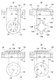
図3は、センサーアレイ基板11に設けられる超音波トランスデューサー100および受信トランスデューサー200のアレイ配置構造の例を示す図である。
図3に示すように、センサーアレイ基板11の基板面に対して直交する方向から当該センサーアレイ基板11を見た平面視(センサー平面視)において、センサーアレイ基板11には、超音波トランスデューサー100および受信トランスデューサー200が、それぞれX方向およびX方向に直交するY方向に沿って、均等間隔で配置されている。
より具体的には、X方向に沿って互いに隣接する2つの超音波トランスデューサー100、およびこれらの2つの超音波トランスデューサーに対して+Y方向に隣接する2つの超音波トランスデューサー100の間に受信トランスデューサー200が配置されている。つまり、センサーアレイ基板11上の各トランスデューサー100,200の配置領域に、X軸座標およびY軸座標を設定した場合、超音波トランスデューサー100は(2n+1,2m+1)(n,mは自然数)の位置にそれぞれ配置され、受信トランスデューサー200は、(2n,2m)(n,mは自然数)の位置にそれぞれ配置される。
FIG. 3 is a diagram illustrating an example of an array arrangement structure of the
As shown in FIG. 3, when the
More specifically, reception is performed between two
このように、超音波トランスデューサー100をセンサーアレイ基板11にアレイ状均等配置することで、超音波を効率的にPDA1の表示部3上に発信することができ、また、各超音波トランスデューサー100における超音波発信タイミングを制御することで、所定位置に超音波を集束させることが可能となる。また、センサーアレイ基板11上に、アレイ状に受信トランスデューサー200を均等配置することで、例えばPDA1の表示部3上で手や指、ペンなどにより反射された超音波を効率よく受信することができる。すなわち、1つの受信トランスデューサーのみを設ける構成とした場合、この1つの受信トランスデューサーに超音波が戻ってこなかった場合、受信される超音波が弱くなる。これに対して、センサーアレイ基板11にアレイ状に受信トランスデューサー200を設けることで、センサーアレイ基板11上のどの位置に超音波が入力されても、その超音波を適切に受信することができ、超音波が反射された位置をも把握することが可能となる。
In this way, by arranging the
なお、超音波トランスデューサー100および受信トランスデューサー200の配置位置としては、上記に限られず、例えば図4に示すような配置構造としてもよい。図4は、センサーアレイ基板11上の超音波トランスデューサー100および受信トランスデューサー200を配置したアレイ構造の他の例を示す図である。この図4の例では、超音波トランスデューサー100および受信トランスデューサー200は、それぞれ、複数の同心円上に沿って配置される。具体的には、超音波トランスデューサー100は、中心からの半径RがR=R2n-1となる円周上に沿って均等間隔に配置され、受信トランスデューサー200は、中心からの半径RがR=R2nとなる円周上に沿って均等間隔に配置されている。このようなアレイ配置構造であっても、上記図3のアレイ構造と同様に、超音波トランスデューサー100における超音波の発信、および受信トランスデューサー200における超音波の受信を効率よく実施することができる。
Note that the arrangement positions of the
(3.超音波トランスデューサーの構成)
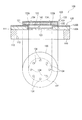
次に、超音波トランスデューサー100の具体的な構造について、図面に基づいて説明する。図5は、超音波トランスデューサー100をセンサーアレイ基板11の厚み方向に沿って断面した状態を模式的に示す断面図、および超音波トランスデューサー100を構成する圧電体の概略構成を示す平面図である。なお、図5の上側に図示した断面図において、図面上側が超音波トランスデューサー100の裏側であり、図面下側が超音波の出力方向となる表側となる。図6は、超音波トランスデューサー100を駆動させた状態を示す断面図である。
(3. Configuration of ultrasonic transducer)
Next, a specific structure of the
図5に示すように、超音波トランスデューサー100は、支持部110と、ダイアフラム120と、圧電体130とを備えている。
支持部110は、上記したように、センサーアレイ基板11の超音波トランスデューサー100の配置位置に形成される部分である。ここで、以降の説明において、センサーアレイ基板11のダイアフラム120が積層される面をダイアフラム形成面111と称し、ダイアフラム形成面111とは反対側となる超音波の出力方向側の面を出力側面112と称す。
この支持部110には、超音波を出力する内周円筒形状の開口部113が形成されている。この開口部113は、例えばセンサー平面視において略円形に形成され、ダイアフラム形成面111から出力側面112を貫通する形状に形成されている。
As shown in FIG. 5, the
As described above, the
The
ダイアフラム120は、ダイアフラム形成面111に形成され、開口部113を閉塞する。このダイアフラム120は、厚み寸法が例えば1μmとなる膜状部材であり、例えばスパッタリングや蒸着などの手法によりセンサーアレイ基板11(支持部110)上に成膜される。また、本実施形態では、このダイアフラム120は、2層構成により形成され、例えば支持部110上にSiO2層120Aを成膜し、このSiO2層120AにZrO2層120Bを成膜することで形成されている。ここで、ZrO2層120Bは、後述する圧電体130の圧電膜131の焼成形成時の圧電膜131の剥離を防止するための層である。すなわち、圧電膜131(例えばPZT)の焼成時、ZrO2層120Bが形成されていない場合、PbがSiO2層120Aに拡散することで、SiO2層120Aの融点が下がり、SiO2層120Aの表面に気泡が生じて、この気泡によりPZTが剥離してしまう。また、ZrO2層120Bがない場合、圧電膜131の歪みに対する撓み効率が低下するなどの問題もある。これに対して、ZrO2層120BがSiO2層120A上に形成される場合、圧電膜131の剥離や、撓み効率の低下などの不都合を回避することが可能となる。
The
このダイアフラム120は、支持部110に形成される開口部113から、超音波トランスデューサー100の超音波出力方向の空間に露出している。また、ダイアフラム120の支持部110と接しない面(以降、圧電体対向面121と称す)には、凹溝部122が形成されている。この凹溝部122は、センサー平面視において、開口部113と同心円となる円形に形成される凹溝である。そして、この凹溝部122の底部123の厚み寸法、すなわち凹溝部122の底面からダイアフラム120の開口部113に臨む面までの寸法は、0.3μm〜0.6μmに形成される。この厚み寸法としては、出力させる超音波の振幅により適宜設定される値であるが、厚み寸法が0.3μmよりも小さくなる場合は、底部123の強度が維持できず、破損するおそれがあり、0.6μmよりも大きくなる場合は、底部123の撓み量が減少し、超音波の振幅が小さくなる。
The
圧電体130は、センサー平面視において、開口部113および凹溝部122と同心円に形成される膜状部材であり、凹溝部122の径寸法より大きく、開口部113の径寸法よりも小さく形成されている。この圧電体130は、圧電膜131と、圧電膜131に電圧を印加する電極(下部電極132および上部電極133)と、を備えている。
圧電膜131は、例えばPZT(ジルコン酸チタン酸鉛:lead zirconate titanate)を膜状に形成することで形成される。なお、本実施形態では、圧電膜131としてPZTを用いるが、電圧を印加することで、面内方向に収縮することが可能な素材であれば、いかなる素材を用いてもよく、例えばチタン酸鉛(PbTiO3)、ジルコン酸鉛(PbZrO3)、チタン酸鉛ランタン((Pb、La)TiO3)などを用いてもよい。
The
The
下部電極132および上部電極133は、圧電膜131を挟んで形成される電極であり、下部電極132は、圧電膜131のダイアフラム120に対向する面に形成され、上部電極133は、圧電膜131のダイアフラム120に対向する面とは反対側の裏面側に形成されている。これらの上部電極133および下部電極132は、それぞれダイアフラム120の裏面側に形成される図示しない引出部により引き出されて、フレキシブル基板12に接続されており、演算制御部から入力される電圧信号により圧電膜131に所定の電圧を印加する。
The
上記のような圧電体130は、ダイアフラム120の凹溝部122を覆う状態に形成される。
具体的には、圧電体130は、図5に示すように、支持部110の開口部113の内周側で、かつダイアフラム120の凹溝部122の外周側の領域に密着固定されている。これにより、圧電体130は、凹溝部122に対向する面が撓むことなく、凹溝部122の底部123から所定の隙間寸法の空間140を介して配置される。
また、圧電体130には、図5の平面図にも示すように、本発明の連通部である複数の平面視円形の連通孔134が、凹溝部122の外周縁に対向する位置に均等に形成されている。この連通孔134は、圧電体130の厚み方向に沿って貫通形成され、ダイアフラム120および圧電体130の間に形成される空間140と、外部空間とを連通している。
The
Specifically, as shown in FIG. 5, the
Further, as shown in the plan view of FIG. 5, the
そして、上記のような超音波トランスデューサー100では、演算制御部から圧電体130の電極132,133間に所定の駆動電圧が印加されると、図6に示すように、圧電膜131が面内方向に収縮する。これにより、圧電体130が固定されるダイアフラム120の凹溝部122の外側領域が凹溝部122の内周側に引っ張られる。これにより、凹溝部122の内周壁122Aも凹溝部122の中心軸方向に変位し、凹溝部122の底部123は、図6に示すように、超音波出力方向に向かって撓む。また、圧電膜131への電圧が切られたり、負電圧が印加されたりすると、圧電膜131は、図5に示すような初期状態に戻る。すなわち、駆動電圧として交流電圧を印加することで、圧電体130が面方向に対して伸縮し、これにより凹溝部122の底部123が前記面方向に対して直交する方向に振動するため、底部123の振動量に応じた超音波が連続的に出力方向に対して出力される。この時、圧電体130は、凹溝部122に対向する領域において、空間140を介して配置され、ダイアフラム120に密着固定されていないため、抵抗がなく、収縮量が大きくなる。また、圧電体130の収縮量を底部123の面方向に直交する方向への変位に変換するので、圧電体130の収縮量に対して、底部123の変位量が大きくなる。以上により、底部123の変位量が増幅されることで、大音圧の超音波を出力することが可能となる。
In the
(4.受信トランスデューサーの構成)
次に、センサーアレイ基板11の形成される受信トランスデューサー200の構成について、説明する。図7は、受信トランスデューサーの概略構成を示す断面図である。
受信トランスデューサー200は、図7に示すように、第二支持部210と、第二ダイアフラム220と、第二圧電体230とを備えている。なお、本実施の形態では、この受信トランスデューサー200は、図2〜図4に示すように、センサー平面視において、超音波トランスデューサー100の径寸法よりも小さい径寸法に形成されているが、これに限定されるものではなく、例えば超音波トランスデューサー100と同程度の大きさや、より大きい径寸法に形成される構成としてもよい。
第二支持部210は、上記したように、センサーアレイ基板11の受信トランスデューサー200の配置位置に形成される部分である。この第二支持部210には、超音波が入力される第二開口部213が形成されている。この第二開口部213は、例えばセンサー平面視において略円形に形成され、この第二開口部213には、入力された超音波により変位する第二ダイアフラム220が臨んで設けられている。
(4. Configuration of receiving transducer)
Next, the configuration of the receiving
As shown in FIG. 7, the receiving
As described above, the
第二ダイアフラム220は、第二支持部210の裏面(ダイアフラム形成面111)側に形成される。この第二ダイアフラム220は、ダイアフラム120と同様に、厚み寸法が例えば1μmとなる膜状部材であり、例えばスパッタリングや蒸着などの手法により、ダイアフラム120の形成時に同時に形成される。すなわち、第二ダイアフラム220は、ダイアフラム120と同様、2層構成により形成され、例えばセンサーアレイ基板11上にSiO2層120Aを成膜し、このSiO2層120AにZrO2層120Bを成膜することで形成されている。本実施形態では、ダイアフラム120および第二ダイアフラム220がセンサーアレイ基板11の基板上で連続して形成されている。なお、これに限定されず、これらのダイアフラム120および第二ダイアフラム220が、センサーアレイ基板11の基板上で連続せず、それぞれ別部材として形成される構成であってもよい。
また、受信トランスデューサー200における第二ダイアフラム220は、裏面が平面状に形成され、凹溝部122は形成されない。
The
Further, the
第二圧電体230は、第二ダイアフラム220上に密接して形成されており、第二ダイアフラム220が撓むと、第二圧電体230も同一撓み量だけ撓む。この第二圧電体230は、第二圧電膜231と、第二圧電膜231に電圧を印加する電極(下部電極232および上部電極233)と、を備えている。
第二圧電膜231は、超音波トランスデューサー100の圧電膜131と同様に、膜状のPZTにより形成される。なお、第二圧電膜231においても、上記PZTに限らず、例えばチタン酸鉛(PbTiO3)、ジルコン酸鉛(PbZrO3)、チタン酸鉛ランタン((Pb、La)TiO3)などを用いてもよい。
下部電極232および上部電極233は、第二圧電膜231を挟んで形成される電極であり、下部電極232は、第二圧電膜231の第二ダイアフラム220に対向する面に形成され、上部電極233は、第二圧電膜231の下部電極232が形成される面とは反対側となる裏面側に形成されている。これらの上部電極233および下部電極232は、それぞれ第二ダイアフラム220の裏面側に形成される図示しない引出部により引き出されて、フレキシブル基板12に接続されている。
The second
Similar to the
The
そして、上記のような受信トランスデューサー200では、第二開口部213から超音波が入力されると、その超音波の強さに応じて第二ダイアフラム220が振動し、第二ダイアフラム220に密着固定される第二圧電体230も振動する。そして、第二圧電膜231は、第二圧電体230の振動により撓み、その撓み量に応じた電気信号を、上部電極233および下部電極232からフレキシブル基板12を介して、演算制御部に出力する。
In the receiving
(5.超音波センサーの製造)
次に、上述したような超音波センサー10の製造方法について、図面に基づいて説明する。
図8から図12は、超音波センサー10の製造工程を示す図であり、各図における左側に各工程における超音波トランスデューサー100の断面、右側に各工程における受信トランスデューサー200の断面を示す。
本実施形態では、超音波センサー10は、センサーアレイ基板11上に、超音波トランスデューサー100および受信トランスデューサー200を同時に形成することで、製造効率の向上が図られている。すなわち、超音波センサー10の製造では、センサーアレイ基板11上にダイアフラム120および第二ダイアフラム220を形成するダイアフラム形成工程を実施する。
(5. Production of ultrasonic sensors)
Next, a method for manufacturing the
FIG. 8 to FIG. 12 are diagrams showing the manufacturing process of the
In this embodiment, the
これには、まず、図8(A)に示すように、開口部113および第二開口部213が形成されていない平板状のセンサーアレイ基板11の表面に、ダイアフラム形成用のSiO2層120Aを成膜する(ダイアフラム積層工程,第二ダイアフラム積層工程)。このSiO2層120Aは、基板面全体(出力方向側の面、ダイアフラム形成側の面、および側面)に形成される。
そして、図8(B)に示すように、このSiO2層120A上に、超音波トランスデューサー100の凹溝部122を形成するためのレジスト150Aを成膜する。すなわち、凹溝部122の形成位置以外をレジスト150Aによりマスクする。
この後、図8(C)に示すように、ICP(Inductive Coupled Plasma)エッチング装置を用いたRIE(Reactive Ion Etching)により、レジスト150Aが成膜されていない範囲のSiO2層をエッチングし、凹溝部122を形成する(凹溝形成工程)。なお、本実施形態では、成膜されたSiO2層120Aを高精度によりエッチングして凹溝部122を形成する必要があるため、ICPエッチング装置によるRIE(ICP−RIE)を用いることが好ましいが、他のエッチング方法を用いてもよい。この時、凹溝部122の深さ寸法が、例えば0.5μmとなるように、このSiO2層のエッチングを実施する。なお、溝深さが0.5μmである凹溝部122を形成したが、上述したように、凹溝部122の深さ寸法としては、0.3〜0.6μmの間で適宜設定されればよい。
この後、図8(D)に示すように、凹溝部122形成用のレジスト150Aを除去し、図9(A)に示すように、SiO2層120A上にZrO2層120Bを形成する。このZrO2層は、例えば0.26μmのZrを成膜し、RTA酸化(Rapid Thermal Annealing)により、0.4μmのZrO2層120Bを成膜する。
以上により、超音波トランスデューサー100のダイアフラム120および受信トランスデューサー200の第二ダイアフラム220が製造される。
First, as shown in FIG. 8A, a diaphragm forming SiO 2 layer 120A is formed on the surface of the flat
Then, as shown in FIG. 8B, a resist 150A for forming the
Thereafter, as shown in FIG. 8C, the SiO 2 layer where the resist 150A is not formed is etched by RIE (Reactive Ion Etching) using an ICP (Inductive Coupled Plasma) etching apparatus.
Thereafter, as shown in FIG. 8D, the resist 150A for forming the
Thus, the
このダイアフラム形成工程の後、ダイアフラム120の凹溝部122に犠牲層151を埋め込む犠牲層埋め込み工程を実施する。
これには、図9(B)に示すように、ダイアフラム120および第二ダイアフラム220のZrO2層120B上に、犠牲層151を形成する。この犠牲層151としては、例えばシリコン(Si)を用いる。また、犠牲層151の形成には、凹凸面がある表面に対しても一様な厚みで成膜が可能な成膜方法が好ましく、本実施形態では、CVD(Chemical Vapor Deposition:化学気相蒸着)を用いる。この時、凹溝部122の深さ寸法以上となるように、犠牲層151を形成し、凹溝部122を犠牲層151で充填させる。
そして、図9(C)に示すように、センサーアレイ基板11上の犠牲層151を、ZrO2層120Bまで研磨することで、凹溝部122に充填された犠牲層151以外を除去する。この時、犠牲層151は、CMP(Chemical Mechanical Polishing:化学機械研磨)により除去することが好ましく、CMPにより、凹溝部122以外に積層される犠牲層151のみを高速に除去することができ、かつ凹溝部122の犠牲層151の表面を平滑にすることが可能となる。
After this diaphragm forming step, a sacrificial layer embedding step for embedding the
To this end, as shown in FIG. 9B, a
Then, as shown in FIG. 9C, the
そして、犠牲層埋め込み工程の後、圧電体130および第二圧電体230を形成するための膜を積層する圧電体積層工程を実施する。
この圧電体積層工程では、まず、図9(D)に示すように、上記犠牲層埋め込み工程の後のダイアフラム120(第二ダイアフラム220)上に、下部電極132,232形成用の導電性膜152をスパッタリングにより形成する。本実施形態では、この導電性膜152として、例えばTi/Ir/Pt/Tiの積層構造膜を用い、膜厚さは圧電膜131(第二圧電膜231)の焼成後で0.2μmとなるように形成する。
この後、図10(A)に示すように、導電性膜152の表面に圧電膜131および第二圧電体230を形成するためのPZT膜153を成膜する。このPZT膜153は、MOD(Metal Organic Decomposition)法を用い、12層の膜により、例えばトータル厚み寸法が1.4μmとなるように形成する。
そして、図10(B)に示すように、上記のように形成されたPZT膜153上に、上部電極133,233形成用の導電性膜154をスパッタリングにより形成する。この上部電極133,233形成用の導電性膜154としては、例えばIr膜を用い、厚み寸法が例えば50nmとなるように形成する。
Then, after the sacrificial layer embedding step, a piezoelectric layer stacking step is performed in which films for forming the
In this piezoelectric layer stacking step, first, as shown in FIG. 9D, the
Thereafter, as shown in FIG. 10A, a
Then, as shown in FIG. 10B, a
次に、この圧電体積層工程の後、圧電体130(第二圧電体230)を形成するための圧電体形成工程(第二圧電体形成工程)を実施する。この圧電体形成工程において、本発明の連通部形成工程も同時に実施される。
すなわち、圧電体形成工程(第二圧電体形成工程)では、図10(C)に示すように、上部電極形成用の導電性膜154上に、圧電体130および第二圧電体230の形成位置にそれぞれレジスト150Bを形成する。この時、超音波トランスデューサー100の圧電体130を形成するためのレジスト150Bには、連通孔134を形成するための孔部150Cを形成する。この後、図11(A)に示すように、ICP−RIEにより、レジスト150Bの成膜部分以外をドライエッチングし、図11(B)に示すように、レジスト150Bを除去する。これにより、圧電体130、第二圧電体230、および圧電体130を貫通する連通孔134が形成される。
Next, after this piezoelectric material lamination step, a piezoelectric material forming step (second piezoelectric material forming step) for forming the piezoelectric material 130 (second piezoelectric material 230) is performed. In this piezoelectric body forming step, the communication portion forming step of the present invention is also performed at the same time.
That is, in the piezoelectric body forming step (second piezoelectric body forming step), as shown in FIG. 10C, the formation positions of the
そして、この圧電体130、第二圧電体230、および連通孔134の形成後、超音波トランスデューサー100の凹溝部122に充填された犠牲層151を除去する犠牲層除去工程を実施する。
この犠牲層除去工程では、連通孔134より例えばXeF2などのエッチングガスを流入させることで、凹溝部122内の犠牲層151(Si)のみを等方性エッチングし、図11(C)に示すように、圧電体130および凹溝部122の底部123との間に空間140を形成する。
なお、この時、センサーアレイ基板11の外周面にダイアフラム形成用のSiO2層120Aが成膜されている場合、センサーアレイ基板11の超音波出力方向側の面のSi基板がエッチングされることはない。一方、センサーアレイ基板11のダイアフラム形成面111にのみSiO2層120Aを形成した場合、センサーアレイ基板11の側面および出力側面112をマスクする必要がある。
Then, after the formation of the
In this sacrificial layer removal step, an etching gas such as XeF 2 is introduced from the
At this time, if the diaphragm forming SiO 2 layer 120A is formed on the outer peripheral surface of the
犠牲層除去工程の後、センサーアレイ基板11を加工して、支持部110および第二支持部210を形成する、本発明の支持体形成工程および第二支持体形成工程である基板加工工程を実施する。
これには、まず、センサーアレイ基板11の厚み寸法を調節する。すなわち、支持部110および第二支持部210における開口部113および第二開口部213を形成する際、エッチング量の深さを浅くするために、センサーアレイ基板11の出力側面112上に形成されたSiO2層120A、およびセンサーアレイ基板11の出力側面112を研削する。ここで、開口部113および第二開口部213は、ICP装置によりエッチング形成するが、エッチングする深さ寸法、膜応力反りに対する剛性、およびハンドリングに対する強度を考慮し、センサーアレイ基板11のSi厚み寸法が200μmとなるように研削することが好ましい。
開口部113および第二開口部213の形成では、図示は省略するが、センサーアレイ基板11の出力側面112に開口部113および第二開口部213の形成位置以外にレジストを形成する。このレジストは、センサーアレイ基板11の200μm深さのエッチングに耐えられるように、例えば10μm程度の厚みに形成する。この後、図12に示すように、ICP装置を用いて、センサーアレイ基板11を、出力側面112からダイアフラム120のSiO2層120Aまでエッチングする。
以上により、超音波トランスデューサー100及び受信トランスデューサー200が複数配置されるセンサーアレイ基板11が製造される。
After the sacrificial layer removing step, the
For this, first, the thickness dimension of the
In the formation of the
Thus, the
なお、本実施形態では、センサーアレイ基板11が支持部110および第二支持部210を構成し、ダイアフラム120および第二ダイアフラム220が一体に形成される例を示したが、例えば、センサーアレイ基板上の所定位置に、それぞれ別体として製造される超音波トランスデューサー100、およびそれぞれ別体として製造される受信トランスデューサー200を組み込む構成としてもよい。この場合、上記製造方法において、センサーアレイ基板11を、超音波トランスデューサー100の支持部110、受信トランスデューサー200の第二支持部210を構成するSi基板に置き換える。そして、上記製造方法に示すように、超音波トランスデューサー100および受信トランスデューサー200を製造した後、これらの超音波トランスデューサー100、受信トランスデューサー200を、例えばレーザーカットなどにより切断する。これにより、それぞれ別体となる超音波トランスデューサー100および受信トランスデューサー200を製造することができる。
In the present embodiment, the
(6.第一実施形態の作用効果)
上述したように、第一実施形態の超音波センサー10を構成する超音波トランスデューサー100は、支持部110の開口部113にダイアフラム120が形成され、このダイアフラム120の圧電体対向面121に凹溝部122が形成されている。そして、圧電体130は、ダイアフラム120の凹溝部122の外周側に密着固定されることで、この凹溝部122を覆う状態に設けられている。
このような構成の超音波トランスデューサー100では、圧電体130に電圧が印加され、面方内向に収縮すると、凹溝部122の外周壁面が内側に変位され、凹溝部122の底部123が超音波の出力方向に撓み、超音波が出力される。このような構成では、圧電体130の収縮量を増幅させて底部123が変位するため、底部123の撓み量が大きくなる。また、圧電体130と底部123との間に空間140が形成されるため、圧電体130の収縮時の抵抗が小さく、収縮量が大きくなる。
以上により、例えば圧電体130の一面側の全面をダイアフラム上に密着固定するような構成に比べて、凹溝部122の底部123の撓み量を大きくすることができ、大音圧の超音波を出力することができる。
(6. Effects of First Embodiment)
As described above, in the
In the
As described above, for example, compared with a configuration in which the entire surface on one side of the
また、圧電体130に連通孔134が形成されているので、圧電体130とダイアフラム120の凹溝部122との間に上述なような空間を容易に設けることが可能となる。すなわち、超音波トランスデューサー100の一部を構成する圧電体130は、膜状の下部電極132、上部電極、および圧電膜131により形成される。このような膜状の圧電体130をダイアフラム120の凹溝部122の底部123との間に空間を介した状態で形成することは、単にダイアフラム120上に圧電体130を積層するだけでは困難であり、例えば圧電体130が凹溝部122側に撓むなどの問題が発生する。したがって、凹溝部122に犠牲層151を埋め込み、犠牲層151の上から圧電体130を積層することになるが、この場合では、犠牲層の除去が困難となる。これに対して、本実施形態では、圧電体130は、厚み方向を貫通する連通孔134が設けられているため、この連通孔134を通してエッチングガスを流入させるだけで、凹溝部122に形成された犠牲層151を容易に除去することができる。
Further, since the
そして、本実施形態の超音波センサー10は、センサーアレイ基板11上に、超音波トランスデューサー100および受信トランスデューサー200が設けられている。このため、超音波トランスデューサー100で出力した超音波を、受信トランスデューサー200で受信することができる。したがって、1つの基板で超音波の出力および入力の双方を実施することができ、PDA1における部品点数の削減、コストダウンを図ることができる。
In the
また、この超音波センサー10は、センサーアレイ基板11上に、超音波トランスデューサー100および受信トランスデューサー200が2次元アレイ構造に配列されている。超音波トランスデューサー100を2次元アレイ構造に配置することで、大音圧の超音波を所望の位置に向かって出力することができる。また、受信トランスデューサー200を2次元アレイ構造に配置することで、利用者の指やペンなどのより反射された超音波がセンサーアレイ基板11上のどの位置に入力されても、適切にその超音波を捉え、受信することができる。また、受信された超音波の大きさ、位相差などに基づいて、超音波トランスデューサー100により出力された超音波がどの位置で反射されたかを、演算により容易に把握することができる。
In the
そして、本実施形態の超音波トランスデューサー100は、ダイアフラム積層工程、凹溝形成工程、犠牲層埋め込み工程、圧電体形成工程、連通部形成工程、犠牲層除去工程、支持体形成工程である基板加工工程を実施することで製造される。すなわち、超音波トランスデューサー100は、センサーアレイ基板11上のダイアフラム120に凹溝部122を形成し、この凹溝部122に犠牲層151を埋め込む。そして、これらダイアフラム120および犠牲層151の上から、連通孔134を備える圧電体130を形成し、この連通孔134から犠牲層151を除去している。
このような製造方法により、上述したように、凹溝部122に形成された犠牲層151を、連通孔134からエッチングガスを流入させるだけで、容易に除去することができ、圧電体130と凹溝部122の底部123との間に空間140を形成することができる。また、圧電体130の凹溝部122側への撓みも防止することができる。
The
According to such a manufacturing method, as described above, the
また、本実施形態では、超音波センサー10は、超音波トランスデューサー100および受信トランスデューサー200の双方を同時に形成することができる。すなわち、センサーアレイ基板11上にSiO2層120AおよびZrO2層120Bを形成することで、ダイアフラム120および第二ダイアフラム220を同時に形成することができる。また、センサーアレイ基板11のダイアフラム対向面側に圧電体130および第二圧電体230の形成用の下部電極形成用の導電性膜152、PZT膜153、上部電極形成用の導電性膜154を成膜し、レジスト150Bを形成してICP−RIEによりエッチングすることで、圧電体130および第二圧電体230を同時に形成することができる。さらに、センサーアレイ基板11の出力側面112にレジストを形成してICPエッチングすることで、開口部113および第二開口部213を同時に形成することができ、支持部110および第二支持部210を同時に形成することができる。すなわち、本発明のダイアフラム形成工程および第二ダイアフラム形成工程、圧電体形成工程および第二圧電体形成工程、支持体形成工程および第二支持体形成工程を共通に実施することができる。このような製造方法では、受信トランスデューサー200の製造のために、別途製造装置を設け、別の製造工程を実施する必要がなく、超音波トランスデューサー100の製造と同時に、受信トランスデューサー200をも製造することができる。したがって、超音波センサー10の製造を容易にでき、製造コストの低減をも図ることができる。
In the present embodiment, the
〔第二実施形態〕
次に、本発明に係る第二実施形態の超音波センサーについて、図面に基づいて説明する。
第二実施形態の超音波センサーは、第一実施形態のPDA1の超音波センサー10のセンサーアレイ構造を変更したものであり、超音波トランスデューサー100および第二超音波トランスデューサーである受信トランスデューサー200の具体的な構成は同一である。したがって、以下、第二実施形態の超音波センサー10Aのアレイ構造について説明する。
[Second Embodiment]
Next, an ultrasonic sensor according to a second embodiment of the present invention will be described based on the drawings.
The ultrasonic sensor of the second embodiment is obtained by changing the sensor array structure of the
第二実施形態の超音波センサー10Aは、図13(A)に示すように、2枚のセンサーアレイ基板、すなわち超音波送信用センサーアレイ基板11Aと、超音波受信用センサーアレイ基板11Bと、を備えている。
As shown in FIG. 13A, the
超音波送信用センサーアレイ基板11Aは、例えば単結晶シリコン基板などにより形成されている。この超音波送信用センサーアレイ基板11Aには、図13(B)に示すように、複数の超音波トランスデューサー100が、マトリクス状に均等間隔で配置されている。ここで、この超音波送信用センサーアレイ基板11Aは、本発明の支持体を構成している。すなわち、超音波送信用センサーアレイ基板11Aには、超音波トランスデューサー100の配置位置に支持部110および開口部113が設けられている。
また、超音波送信用センサーアレイ基板11Aには、貫通孔11A1がマトリクス状に均等間隔で配置されている。具体的には、この貫通孔11A1は、超音波トランスデューサー100の配置位置に対して、千鳥状に超音波送信用センサーアレイ基板11Aに形成されている。
The ultrasonic transmission
In addition, through holes 11A1 are arranged in a matrix at equal intervals in the ultrasonic transmission
超音波受信用センサーアレイ基板11Bは、例えば単結晶シリコン基板などに形成されている。この超音波受信用センサーアレイ基板11Bには、図13(C)に示すように、複数の受信トランスデューサー200が、マトリクス状に均等間隔で配置されている。より具体的には、図13(A)に示すように、超音波送信用センサーアレイ基板11Aと超音波受信用センサーアレイ基板11Bとを重ね合わせて超音波センサー10Aを形成した際に、超音波送信用センサーアレイ基板11Aの貫通孔11A1から、超音波受信用センサーアレイ基板11Bの受信トランスデューサー200が露出されるように、超音波受信用センサーアレイ基板11Bに受信トランスデューサー200が配置されている。
また、この超音波受信用センサーアレイ基板11Bは、本発明の第二支持体を構成している。すなわち、超音波受信用センサーアレイ基板11Bには、受信トランスデューサー200の配置位置に対応して、第二支持部210および第二開口部213が設けられている。
The ultrasonic reception
Further, the ultrasonic receiving
このような第二実施形態の超音波センサー10Aでは、超音波送信用センサーアレイ基板11Aと、超音波受信用センサーアレイ基板11Bとは、それぞれ別体として製造される。すなわち、図8から図12における左側に示される各工程に従い、ダイアフラム形成工程(ダイアフラム積層工程、凹溝形成工程、ZrO2層120Bの積層工程)、犠牲層埋め込み工程、圧電体積層工程、連通部形成工程を含む圧電体形成工程、犠牲層除去工程、基板加工工程により、超音波トランスデューサー100を備えた超音波送信用センサーアレイ基板11Aを製造する(第一製造工程)。また、図8から図12における右側に示される各工程に従い、ダイアフラム形成工程(第二ダイアフラム積層工程、ZrO2層120Bの積層工程)、圧電体積層工程、第二圧電体形成工程、基板加工工程により、受信トランスデューサー200を備えた超音波受信用センサーアレイ基板11Bを製造する(第二製造工程)。そして、これらの第一製造工程、および第二製造工程においてそれぞれ製造された超音波送信用センサーアレイ基板11Aおよび超音波受信用センサーアレイ基板11Bを重ね合わせて接合することで、超音波センサー10Aが製造される。
In the
上述のような第二実施形態の超音波センサー10Aにおいても、第一実施形態と同様の構成の超音波トランスデューサー100が設けられるため、上記第一実施形態と同様の作用効果が得られる。すなわち、超音波トランスデューサー100の底部123の撓み量が大きくでき、大音圧の超音波を出力することができる。
Also in the
また、第二実施形態の超音波センサー10Aでは、超音波送信用センサーアレイ基板11Aと、超音波受信用センサーアレイ基板11Bとが別体として製造され、これらの基板を重ね合わせることで、超音波センサー10Aが形成される。このような構成では、例えば超音波送信用センサーアレイ基板11Aや、超音波受信用センサーアレイ基板11Bを単体で用いるセンサーにも適用することができる。
さらに、各基板11A,11Bには、各トランスデューサー100,200の電極132,133,232,233と演算制御部とを接続する配線パターンを形成する必要がある。ここで、第一実施形態のように、1つのセンサーアレイ基板11に超音波トランスデューサー100用の配線パターン、および受信トランスデューサー200用の配線パターンを設ける場合、各配線パターン間の間隔が小さく、製造が困難となる場合もある。これに対して、第二実施形態のように、超音波センサー10Aを、超音波送信用センサーアレイ基板11Aと、超音波受信用センサーアレイ基板11Bとに分けることで、各基板11A,11Bに形成する配線パターンの間隔も大きく採れ、より容易に製造することが可能となる。
Further, in the
Furthermore, it is necessary to form wiring patterns for connecting the
〔変形例〕
なお、本発明は前述の実施形態に限定されるものではなく、本発明の目的を達成できる範囲での変形、改良等は本発明に含まれるものである。
[Modification]
It should be noted that the present invention is not limited to the above-described embodiments, and modifications, improvements, and the like within the scope that can achieve the object of the present invention are included in the present invention.
例えば、上記実施形態では、圧電体130は、凹溝部122の外周縁に沿って円形状の連通孔134が形成される例を示したが、これに限定されず、例えば、図14に示すような形状であってもよい。なお、図14、および以降に説明する図15、図16では、各構成をより簡略化して示したものであり、ダイアフラム120のSiO2層120A,ZrO2層120Bの図示、圧電体130の圧電膜131、下部電極132、および上部電極133の図示を省略する。
すなわち、図14に示すように、連通孔134の形状としては、例えば図14(A)に示すように、センサー平面視において、矩形状に形成され、これらの矩形状の連通孔134が放射状に配置されるものであってもよく、図14(D)に示すように、扇状の連通孔134が配置されるものであってもよい。
For example, in the above-described embodiment, the
That is, as shown in FIG. 14, the shape of the
また、図14(B)に示すように、圧電体130が、凹溝部122の外周径寸法より小さい円形状の圧電本体部130Aと、この圧電本体部130Aから外周方向に延びる複数の接続部130Bと、を備え、接続部130Bがダイアフラム120の凹溝部122の外側領域に密着固定される構成としてもよい。なお、接続部130Bとしては、図14(B)には、4つの接続部130Bが十字方向に延出するものを示すが、3つ以下の接続部130Bが例えば120度間隔で配置される構成としてもよく、5つ以上の接続部130Bが均等角度間隔で放射状に延出する構成であってもよい。このような構成では、各接続部130B間において、圧電本体部130Aの外周縁と凹溝部122の外周縁との間に隙間130Cが形成され、この隙間130Cが本発明の連通部を構成する。
また、連通孔134が形成される位置としては、凹溝部122の外周縁に沿って形成される構成に限らず、図14(C)に示すように、圧電体130の中心位置に形成される構成であってもよい。
Further, as shown in FIG. 14B, the
Further, the position where the
さらに、凹溝部122として、センサー平面視において、円形状のものに限られず、その他いかなる形状であってもよい。例えば、図15に示すように、センサー平面視において、正方形状に形成される構成であってもよい。この場合、圧電体130の形状としては、凹溝部122の形状に対応して、正方形状に形成してもよい。また、連通孔134の形成位置としては、上記実施形態や、図14の例と同様に形成することができる。すなわち、図15(A)(B)に示すように、凹溝部122の外周縁に沿って連通孔134が形成される構成であってもよく、各連通孔134の形状も正方形状、長方形状の他、円形状などとしてもよい。さらに、図14(B)と同様に、図15(c)に示すように、圧電体130は、正方形状の凹溝部122よりも小さい面積の圧電本体部130A、およびこの圧電本体部130Aから外周方向に延びる接続部130Bとを備える構成としてもよく、この場合は、上述したように、圧電本体部130Aの外周縁と凹溝部122の外周縁との隙間130Cを連通部とすることができる。さらに、図14(C)と同様に、図15(D)に示すように、圧電体130の中心部に連通孔134を形成する構成などとしてもよい。
さらには、図16に示すように、円形状の凹溝部122に対して、正方形状など多角形状の圧電体130を設ける構成としてもよく、正方形状など、多角形状の凹溝部122に対して、円形状の圧電体130を設ける構成などとしてもよい。
Further, the
Furthermore, as shown in FIG. 16, it is good also as a structure which provides the polygonal-shaped
また、上記実施形態では、超音波トランスデューサー100および受信トランスデューサー200を同時に製造可能な製造方法により、超音波センサー10を製造したが、超音波トランスデューサー100および受信トランスデューサー200をそれぞれ別工程で、製造してもよい。
また、上述したように、実施形態の製造方法により、所定の基板上に超音波トランスデューサー100および受信トランスデューサー200を製造し、これらの超音波トランスデューサー100および受信トランスデューサー200をレーザーカットなどにより切断して、それぞれ単体のトランスデューサーとして用いてもよい。このような場合でも、超音波トランスデューサー100および受信トランスデューサー200を同時に製造することができ、製造効率を向上させることができるとともに、例えば、センサーアレイ基板11上で、各トランスデューサー100,200のアレイ配置位置を変更したい場合など、適宜取り外しが可能であり、利用の拡大を図ることができる。
Further, in the above-described embodiment, the
In addition, as described above, the
また、上記実施形態では、受信トランスデューサー200は、跳ね返った超音波を受信するセンサー素子としてセンサーアレイ基板11上に配置されているが、例えば受信トランスデューサー200に電圧を印加することで、超音波を出力させることもできる。この場合、例えば超音波トランスデューサー100により出力される超音波と、受信トランスデューサー200により出力される超音波とで、異なる音圧を出力させることができ、それぞれ異なる用途に用いることもできる。
In the above embodiment, the receiving
また、上記実施形態では、超音波トランスデューサー100と受信トランスデューサー200との配置関係を、千鳥状に配置したり同心円状に配置したりしているが、例えば、図17及び図18に示すように、センサーアレイ基板11における略中央領域に複数の超音波トランスデューサーを有する送信アレイを配置し、中央領域の周辺の少なくとも3箇所以上の領域(例えば4箇所)に複数の受信トランスデューサーを有する受信アレイを配置するようにしてもよい。図17及び図18は、超音波センサーの構成の変形例を示す模式平面図である。
In the above embodiment, the
まず、図17に示す超音波センサー10Bの構造について説明する。超音波センサー10Bは、センサーアレイ基板11における略中央の領域に送信アレイ301が配置されている。また、中央領域の周辺の四方に受信アレイ302(第1受信アレイ302a、第2受信アレイ302b、第3受信アレイ302c、第4受信アレイ302d)が配置されている。
First, the structure of the
送信アレイ301には、複数の超音波トランスデューサー100が、マトリクス状に設けられている。各受信アレイ302a,302b,302c,302dには、複数の受信トランスデューサー200が、マトリクス状に設けられている。
The
送信アレイ301に設けられた超音波トランスデューサー100は、図示しない外部の制御回路と接続された送信駆動電極線303と電気的に接続されている。また、各受信アレイ302a,302b,302c,302dに設けられた受信トランスデューサー200も同様に、図示しない外部の制御回路と接続された受信検出電極線304と接続されている。これら、複数の送信駆動電極線303、及び複数の受信検出電極線304は、その一端がセンサーアレイ基板11の一辺に集まるように延在している。
The
また、受信アレイ302a,302dと送信アレイ301の間、及び、受信アレイ302b,302cと送信アレイ301との間には、一端がGNDと接続された定電位配線305が設けられている。つまり、定電位配線305を挟んで送信アレイ301と受信アレイ302とが配置されている。
A constant
これにより、送信アレイ301に設けられた超音波トランスデューサー100と、受信アレイ302に設けられた受信トランスデューサー200との間に、電気ノイズが発生することを防ぐことができる。具体的には、超音波トランスデューサー100が超音波を送信した際に発生した電気ノイズを、定電位配線305によって除去することができる。加えて、定電位配線305が設けられていることにより、受信トランスデューサー200に振動ノイズが伝わることを抑えることができる。
Thereby, it is possible to prevent electrical noise from being generated between the
次に、図18に示す超音波センサー10Cの構造について説明する。超音波センサー10Cは、図17に示す超音波センサー10Bと略同様に、センサーアレイ基板11における略中央の領域に送信アレイ401が配置されている。また、中央領域の周辺の四方に受信アレイ402(第1受信アレイ402a、第2受信アレイ402b、第3受信アレイ402c、第4受信アレイ402d)が配置されている。
Next, the structure of the
図17に示す超音波センサー10Bと同様に、送信アレイ401には、複数の超音波トランスデューサー100が、マトリクス状に設けられている。各受信アレイ402a,402b,402c,402dには、複数の受信トランスデューサー200が、マトリクス状に設けられている。
Similar to the
送信アレイ401に設けられた超音波トランスデューサー100は、図示しない外部の制御回路と接続された送信駆動電極線403と電気的に接続されている。また、各受信アレイ402a,402b,402c,402dに設けられた受信トランスデューサー200は、図示しない外部の制御回路と接続された受信検出電極線404と接続されている。
The
送信駆動電極線403は、例えば、送信アレイ401を構成する4つの辺からその辺に対して略垂直方向に向かって延在している。受信検出電極線404は、例えば、受信アレイ402を構成する4つの辺のうち2つの辺からその辺に対して略垂直方向に向かって延在している。
For example, the transmission
なお、図17に示す超音波センサー10Bと同様に、各受信アレイ402a,402b,402c,402dと送信アレイ401との間に、一端がGNDと接続された定電位配線405が設けられている。
Similarly to the
また、図17に示す超音波センサー10B、及び図18に示す超音波センサー10Cのように、センサーアレイ基板11(共通基板)に送信アレイ301,401及び受信アレイ302,402を設けることに限定されず、それぞれ別々の基板に送信アレイ301,401や受信アレイ302,402を形成し、これらを組み合わせて使用するようにしてもよい。
Moreover, it is limited to providing the
その他、本発明の実施の際の具体的な構造および手順は、本発明の目的を達成できる範囲で他の構造などに適宜変更できる。 In addition, the specific structure and procedure for carrying out the present invention can be appropriately changed to other structures and the like within a range in which the object of the present invention can be achieved.
10,10A,10B,10C…超音波センサー、11…センサーアレイ基板、100…超音波トランスデューサー、110…支持体である支持部、120…ダイアフラム、130…圧電体、130C…連通部である隙間、134…連通孔、140…空間、151…犠牲層、200…第二超音波トランスデューサーである受信トランスデューサー、210…第二支持体である第二支持部、220…第二ダイアフラム、230…第二圧電体、305,405…定電位配線。
DESCRIPTION OF
Claims (9)
前記開口部を閉塞するダイアフラムと、
前記ダイアフラムに設けられるとともに、電圧の印加により面内方向に伸縮する圧電体と、を備え、
前記ダイアフラムは、前記開口部に臨む一面側とは反対側の面に、凹状に形成される凹溝部を備え、
前記圧電体は、前記ダイアフラムにおける前記凹溝部の外側に固定されて、前記凹溝部を覆って配置され、前記凹溝部の底面との間に空間を介して対向配置されることを特徴とする超音波トランスデューサー。 A support having an opening;
A diaphragm for closing the opening;
A piezoelectric body that is provided on the diaphragm and expands and contracts in the in-plane direction when a voltage is applied;
The diaphragm includes a concave groove formed in a concave shape on a surface opposite to the one surface facing the opening,
The piezoelectric body is fixed to the outside of the concave groove portion of the diaphragm, is disposed so as to cover the concave groove portion, and is disposed to face the bottom surface of the concave groove portion via a space. Sonic transducer.
前記圧電体は、前記凹溝部に対向する位置に、前記空間および外部空間を連通する少なくとも1つ以上の連通部を有することを特徴とする超音波トランスデューサー。 The ultrasonic transducer according to claim 1.
The ultrasonic transducer according to claim 1, wherein the piezoelectric body has at least one communicating portion that communicates the space and the external space at a position facing the concave groove portion.
第二開口部を有する第二支持体、前記第二開口部を閉塞する第二ダイアフラム、および前記第二ダイアフラム上に積層され、前記第二ダイアフラムの変位を電気信号に変換して出力する第二圧電体を備えた第二超音波トランスデューサーと、
を備えることを特徴とする超音波センサー。 The ultrasonic transducer according to claim 1 or 2,
A second support having a second opening, a second diaphragm for closing the second opening, and a second diaphragm stacked on the second diaphragm, and converting the displacement of the second diaphragm into an electrical signal for output. A second ultrasonic transducer with a piezoelectric body;
An ultrasonic sensor comprising:
前記超音波トランスデューサーおよび前記第二超音波トランスデューサーは、複数設けられ、二次元アレイ構造に配置されることを特徴とする超音波センサー。 The ultrasonic sensor according to claim 3.
A plurality of the ultrasonic transducers and the second ultrasonic transducers are provided and arranged in a two-dimensional array structure.
前記超音波トランスデューサーは、前記二次元アレイ構造における中央領域に設けられており、
前記第二超音波トランスデューサーは、前記中央領域の周辺において三箇所以上の領域に設けられており、
前記超音波トランスデューサーと前記第二超音波トランスデューサーとの間の領域に定電位と接続された定電位配線が設けられていることを特徴とする超音波センサー。 The ultrasonic sensor according to claim 4,
The ultrasonic transducer is provided in a central region of the two-dimensional array structure,
The second ultrasonic transducer is provided in three or more areas around the central area,
An ultrasonic sensor, wherein a constant potential wiring connected to a constant potential is provided in a region between the ultrasonic transducer and the second ultrasonic transducer.
前記超音波トランスデューサーの前記支持体、および前記第二超音波トランスデューサーの前記第二支持体を構成するセンサーアレイ基板を備えることを特徴とする超音波センサー。 The ultrasonic sensor according to claim 3 or claim 5,
An ultrasonic sensor comprising: a sensor array substrate constituting the support of the ultrasonic transducer and the second support of the second ultrasonic transducer.
基板上にダイアフラム形成用膜を形成するダイアフラム積層工程と、
前記ダイアフラム形成用膜の表面の一部をエッチングにより除去し、凹溝部を形成する凹溝形成工程と、
前記凹溝部に、表面が前記ダイアフラム形成用膜の表面と同一平面となる犠牲層を埋める犠牲層埋め込み工程と、
前記凹溝部を覆う圧電体を形成する圧電体形成工程と、
前記圧電体に外部空間と前記犠牲層とを連通する連通部を形成する連通部形成工程と、
前記連通部から前記犠牲層を除去する犠牲層除去工程と、
前記基板をエッチングして開口部を形成し、支持体を形成する支持体形成工程と、
を備えたことを特徴とする超音波トランスデューサーの製造方法。 An ultrasonic transducer manufacturing method comprising:
A diaphragm laminating step of forming a diaphragm forming film on the substrate;
A part of the surface of the diaphragm forming film is removed by etching to form a concave groove part , and
A sacrificial layer embedding step of burying a sacrificial layer whose surface is flush with the surface of the diaphragm forming film in the concave groove portion;
A piezoelectric body forming step of forming a piezoelectric body covering the concave groove portion;
A communication part forming step of forming a communication part for communicating the external space and the sacrificial layer in the piezoelectric body;
A sacrificial layer removing step of removing the sacrificial layer from the communicating portion;
A support forming step of forming the opening, to form a support for the substrate by etching,
A method for manufacturing an ultrasonic transducer, comprising:
請求項7に記載の超音波トランスデューサーの製造方法により前記超音波トランスデューサーを製造する第一製造工程と、
基板上に第二ダイアフラムを形成する第二ダイアフラム積層工程、
前記第二ダイアフラム上に第二圧電体を積層形成する第二圧電体形成工程、
および、前記基板をエッチングして第二開口部を形成し、第二支持体を形成する第二支持体形成工程、を備える第二製造工程と、
を具備したことを特徴とする超音波センサーの製造方法。 A method of manufacturing an ultrasonic sensor,
A first manufacturing step of manufacturing the ultrasonic transducer by the method of manufacturing an ultrasonic transducer according to claim 7;
Second diaphragm laminating step of forming a second diaphragm on the substrate,
A second piezoelectric body forming step of laminating and forming a second piezoelectric body on the second diaphragm;
And, a second manufacturing process having a second support formation step, of the substrate to form a second opening is etched to form a second support member,
A method of manufacturing an ultrasonic sensor, comprising:
前記ダイアフラム積層工程および前記第二ダイアフラム積層工程、前記圧電体形成工程および前記第二圧電体形成工程、前記支持体形成工程および前記第二支持体形成工程は、それぞれ同一工程であることを特徴とする超音波センサーの製造方法。 In the manufacturing method of the ultrasonic sensor according to claim 8,
The diaphragm laminating step and the second diaphragm laminating step, the piezoelectric body forming step and the second piezoelectric body forming step, the support body forming step and the second support body forming step are the same steps, respectively. Of manufacturing an ultrasonic sensor.
Priority Applications (2)
| Application Number | Priority Date | Filing Date | Title |
|---|---|---|---|
| JP2010182113A JP5671876B2 (en) | 2009-11-16 | 2010-08-17 | Ultrasonic transducer, ultrasonic sensor, method for manufacturing ultrasonic transducer, and method for manufacturing ultrasonic sensor |
| US12/946,061 US8536763B2 (en) | 2009-11-16 | 2010-11-15 | Ultrasonic transducer, ultrasonic sensor, method of manufacturing ultrasonic transducer, and method of manufacturing ultrasonic sensor |
Applications Claiming Priority (3)
| Application Number | Priority Date | Filing Date | Title |
|---|---|---|---|
| JP2009260679 | 2009-11-16 | ||
| JP2009260679 | 2009-11-16 | ||
| JP2010182113A JP5671876B2 (en) | 2009-11-16 | 2010-08-17 | Ultrasonic transducer, ultrasonic sensor, method for manufacturing ultrasonic transducer, and method for manufacturing ultrasonic sensor |
Publications (3)
| Publication Number | Publication Date |
|---|---|
| JP2011124973A JP2011124973A (en) | 2011-06-23 |
| JP2011124973A5 JP2011124973A5 (en) | 2013-09-12 |
| JP5671876B2 true JP5671876B2 (en) | 2015-02-18 |
Family
ID=44010784
Family Applications (1)
| Application Number | Title | Priority Date | Filing Date |
|---|---|---|---|
| JP2010182113A Active JP5671876B2 (en) | 2009-11-16 | 2010-08-17 | Ultrasonic transducer, ultrasonic sensor, method for manufacturing ultrasonic transducer, and method for manufacturing ultrasonic sensor |
Country Status (2)
| Country | Link |
|---|---|
| US (1) | US8536763B2 (en) |
| JP (1) | JP5671876B2 (en) |
Families Citing this family (43)
| Publication number | Priority date | Publication date | Assignee | Title |
|---|---|---|---|---|
| CN103181194A (en) * | 2010-11-01 | 2013-06-26 | Nec卡西欧移动通信株式会社 | Electronic equipment |
| DE102011076430A1 (en) * | 2011-05-25 | 2012-11-29 | Robert Bosch Gmbh | Sound wave based sensor |
| US8861752B2 (en) | 2011-08-16 | 2014-10-14 | Empire Technology Development Llc | Techniques for generating audio signals |
| JP5834679B2 (en) * | 2011-09-20 | 2015-12-24 | セイコーエプソン株式会社 | Ultrasonic probe and ultrasonic diagnostic imaging apparatus |
| US8723399B2 (en) * | 2011-12-27 | 2014-05-13 | Massachusetts Institute Of Technology | Tunable ultrasound transducers |
| JP5990929B2 (en) | 2012-02-24 | 2016-09-14 | セイコーエプソン株式会社 | Ultrasonic transducer device and probe, electronic device and ultrasonic diagnostic device |
| JP5990930B2 (en) | 2012-02-24 | 2016-09-14 | セイコーエプソン株式会社 | Ultrasonic transducer element chip and probe, electronic device and ultrasonic diagnostic apparatus |
| JP5982868B2 (en) * | 2012-02-28 | 2016-08-31 | セイコーエプソン株式会社 | Ultrasonic sensor, ultrasonic array sensor, and method of manufacturing ultrasonic sensor |
| JP5900107B2 (en) | 2012-03-30 | 2016-04-06 | セイコーエプソン株式会社 | Ultrasonic transducer element chip and probe, electronic device and ultrasonic diagnostic apparatus |
| JP6102075B2 (en) | 2012-03-30 | 2017-03-29 | セイコーエプソン株式会社 | Ultrasonic transducer element chip and probe, electronic device and ultrasonic diagnostic apparatus |
| JP6123171B2 (en) * | 2012-05-21 | 2017-05-10 | セイコーエプソン株式会社 | Ultrasonic transducer, ultrasonic probe and ultrasonic inspection equipment |
| JP6065421B2 (en) | 2012-06-15 | 2017-01-25 | セイコーエプソン株式会社 | Ultrasonic probe and ultrasonic inspection device |
| JP6089499B2 (en) * | 2012-08-28 | 2017-03-08 | セイコーエプソン株式会社 | Ultrasonic transducer device and probe, electronic device and ultrasonic diagnostic device |
| JP6186696B2 (en) * | 2012-10-25 | 2017-08-30 | セイコーエプソン株式会社 | Ultrasonic measuring device, head unit, probe and diagnostic device |
| US20140180117A1 (en) * | 2012-12-21 | 2014-06-26 | Volcano Corporation | Preparation and Application of a Piezoelectric Film for an Ultrasound Transducer |
| JP6175780B2 (en) * | 2013-01-28 | 2017-08-09 | セイコーエプソン株式会社 | Ultrasonic device, ultrasonic probe, electronic device and ultrasonic imaging apparatus |
| KR20150113177A (en) * | 2013-02-02 | 2015-10-07 | 아크리온 시스템즈 엘엘씨 | System for processing substrates using acoustic energy |
| JP6136464B2 (en) * | 2013-03-29 | 2017-05-31 | セイコーエプソン株式会社 | ULTRASONIC TRANSDUCER DEVICE AND PROBE, ELECTRONIC DEVICE, AND ULTRASONIC IMAGING DEVICE |
| WO2015042263A1 (en) * | 2013-09-18 | 2015-03-26 | Akrion Systems Llc | System, apparatus, and method for processing substrates using acoustic energy |
| JP6273743B2 (en) * | 2013-09-30 | 2018-02-07 | セイコーエプソン株式会社 | Ultrasonic device and probe, electronic apparatus and ultrasonic imaging apparatus |
| JP6381195B2 (en) * | 2013-10-22 | 2018-08-29 | キヤノン株式会社 | Capacitance type transducer and manufacturing method thereof |
| JP6221679B2 (en) * | 2013-11-20 | 2017-11-01 | セイコーエプソン株式会社 | Ultrasonic device and probe, electronic apparatus and ultrasonic imaging apparatus |
| JP6265758B2 (en) * | 2014-01-27 | 2018-01-24 | キヤノン株式会社 | Capacitive transducer |
| WO2015119629A2 (en) | 2014-02-08 | 2015-08-13 | Empire Technology Development Llc | Mems dual comb drive |
| WO2015119626A1 (en) * | 2014-02-08 | 2015-08-13 | Empire Technology Development Llc | Mems-based structure for pico speaker |
| WO2015119627A2 (en) | 2014-02-08 | 2015-08-13 | Empire Technology Development Llc | Mems-based audio speaker system with modulation element |
| US10123126B2 (en) | 2014-02-08 | 2018-11-06 | Empire Technology Development Llc | MEMS-based audio speaker system using single sideband modulation |
| JP6314777B2 (en) | 2014-09-30 | 2018-04-25 | セイコーエプソン株式会社 | Ultrasonic sensor and probe and electronic equipment |
| CN104540078A (en) | 2014-12-16 | 2015-04-22 | 歌尔声学股份有限公司 | Micro loudspeaker |
| JP6422792B2 (en) * | 2015-02-06 | 2018-11-14 | 株式会社ダイセル | Ultrasonic transceiver |
| WO2016125702A1 (en) * | 2015-02-06 | 2016-08-11 | 株式会社ダイセル | Ultrasonic-wave transmitting-and-receiving device |
| JP6536792B2 (en) * | 2015-03-25 | 2019-07-03 | セイコーエプソン株式会社 | Ultrasonic sensor and method of manufacturing the same |
| US10367430B2 (en) | 2016-01-11 | 2019-07-30 | Infineon Technologies Ag | System and method for a variable flow transducer |
| CN105843446B (en) * | 2016-03-18 | 2019-10-25 | 京东方科技集团股份有限公司 | Detection components, touch control display apparatus, touch localization method and pressure detection method |
| JP6724502B2 (en) * | 2016-04-06 | 2020-07-15 | セイコーエプソン株式会社 | Ultrasonic device |
| CN107920313A (en) * | 2016-08-27 | 2018-04-17 | 深圳市诺维创科技有限公司 | A kind of miniature piezoelectric ultrasonic transducer and preparation method thereof |
| IT201700010342A1 (en) * | 2017-01-31 | 2018-07-31 | St Microelectronics Srl | MEMS DEVICE INCLUDING A PIEZOELECTRIC ACTUATOR WITH A REDUCED VOLUME |
| CN109160485B (en) * | 2018-08-09 | 2020-09-15 | 南京邮电大学 | Acoustic grating-reflecting surface piezoelectric ultrasonic energy collector and preparation method thereof |
| US11818957B2 (en) | 2019-01-21 | 2023-11-14 | Stmicroelectronics S.R.L. | Piezoelectrically actuated MEMS optical device having a protected chamber and manufacturing process thereof |
| US11275057B2 (en) | 2019-04-03 | 2022-03-15 | Infineon Technologies Ag | Photoacoustic sensor valve |
| CN110366084A (en) * | 2019-06-06 | 2019-10-22 | 七色堇电子科技(上海)有限公司 | A kind of semiconductor devices and preparation method thereof and electronic device |
| TWI793447B (en) * | 2019-09-12 | 2023-02-21 | 美商艾克索影像股份有限公司 | Increased mut coupling efficiency and bandwidth via edge groove, virtual pivots, and free boundaries |
| US11984863B2 (en) | 2020-07-08 | 2024-05-14 | Kampanics, L.L.C. | Sensor with resonator supported on a substrate |
Family Cites Families (11)
| Publication number | Priority date | Publication date | Assignee | Title |
|---|---|---|---|---|
| DE3407980A1 (en) * | 1983-04-20 | 1984-10-25 | Tadashi Tokio/Tokyo Sawafuji | CRYSTAL SOUND GENERATOR |
| JPS6273900A (en) * | 1985-09-26 | 1987-04-04 | Yokogawa Electric Corp | Ultrasonic wave transmission and reception device |
| JPS6386998A (en) * | 1986-09-30 | 1988-04-18 | Matsushita Electric Ind Co Ltd | Piezoelectric sound emitting body |
| JPH06105396A (en) * | 1992-09-22 | 1994-04-15 | Hitachi Constr Mach Co Ltd | Ultrasonic wave probe |
| JPH06233386A (en) * | 1993-02-03 | 1994-08-19 | Nippon Chemicon Corp | Fixed structure for piezoelectric sounder |
| JP2000217195A (en) * | 1999-01-22 | 2000-08-04 | Aiphone Co Ltd | Speaker |
| US6894425B1 (en) * | 1999-03-31 | 2005-05-17 | Koninklijke Philips Electronics N.V. | Two-dimensional ultrasound phased array transducer |
| JP4513596B2 (en) * | 2004-08-25 | 2010-07-28 | 株式会社デンソー | Ultrasonic sensor |
| JP2006319945A (en) * | 2005-04-12 | 2006-11-24 | Osaka Industrial Promotion Organization | Diaphragm sensor element and its manufacturing method |
| KR100781467B1 (en) * | 2006-07-13 | 2007-12-03 | 학교법인 포항공과대학교 | Mems based multiple resonances type ultrasonic transducer for ranging measurement with high directionality using parametric transmitting array in air |
| JP2009260723A (en) * | 2008-04-17 | 2009-11-05 | Asahi Kasei Electronics Co Ltd | Transducer |
-
2010
- 2010-08-17 JP JP2010182113A patent/JP5671876B2/en active Active
- 2010-11-15 US US12/946,061 patent/US8536763B2/en active Active
Also Published As
| Publication number | Publication date |
|---|---|
| US20110115337A1 (en) | 2011-05-19 |
| JP2011124973A (en) | 2011-06-23 |
| US8536763B2 (en) | 2013-09-17 |
Similar Documents
| Publication | Publication Date | Title |
|---|---|---|
| JP5671876B2 (en) | Ultrasonic transducer, ultrasonic sensor, method for manufacturing ultrasonic transducer, and method for manufacturing ultrasonic sensor | |
| US10864553B2 (en) | Piezoelectric transducers and methods of making and using the same | |
| JP5834657B2 (en) | Ultrasonic probe and ultrasonic diagnostic imaging apparatus | |
| JP5754129B2 (en) | Piezoelectric element, piezoelectric sensor, electronic device, and method of manufacturing piezoelectric element | |
| JP5751026B2 (en) | Ultrasonic transducer, biosensor, and method for manufacturing ultrasonic transducer | |
| KR102193843B1 (en) | Acoustic transducer with gap-controlling geometry and method of manufacturing an acoustic transducer | |
| JP6065421B2 (en) | Ultrasonic probe and ultrasonic inspection device | |
| WO2018155276A1 (en) | Ultrasonic sensor | |
| CN107394036A (en) | The electrode configuration of pMUT and pMUT transducer arrays | |
| JP2013539254A (en) | Thin film ultrasonic transducer | |
| WO2017188072A1 (en) | Ultrasonic device, ultrasonic module, and ultrasonic measuring device | |
| JP2019146020A (en) | Ultrasonic sensor, ultrasonic device, and method for manufacturing ultrasonic sensor | |
| WO2018163963A1 (en) | Ultrasound sensor and ultrasound sensor device | |
| Sadeghpour et al. | Bendable piezoelectric micromachined ultrasound transducer (PMUT) arrays based on silicon-on-insulator (SOI) technology | |
| JP2011099675A (en) | Pressure sensor, sensor array, and method of manufacturing pressure sensor | |
| WO2020222212A1 (en) | Actuation of piezoelectric structures with ferroelectric thin films having multiple elements | |
| JP6752727B2 (en) | Ultrasound Transducer and Ultrasound Imaging Device | |
| JP6056905B2 (en) | Piezoelectric element, piezoelectric sensor, and electronic device | |
| JP5673005B2 (en) | Ultrasonic sensor and electronic equipment | |
| JP2019165307A (en) | Ultrasonic sensor | |
| WO2022219717A1 (en) | Ultrasound transducer, distance measurement device, and ultrasound transducer manufacturing method | |
| JP6288235B2 (en) | Ultrasonic probe and ultrasonic inspection device | |
| Sadeghpour et al. | Klik hier als u tekst wilt invoeren. Bendable Piezoele | |
| Luo | High-Performance Micromachined Ultrasonic Transducers |
Legal Events
| Date | Code | Title | Description |
|---|---|---|---|
| A521 | Request for written amendment filed |
Free format text: JAPANESE INTERMEDIATE CODE: A523 Effective date: 20130725 |
|
| A621 | Written request for application examination |
Free format text: JAPANESE INTERMEDIATE CODE: A621 Effective date: 20130725 |
|
| A977 | Report on retrieval |
Free format text: JAPANESE INTERMEDIATE CODE: A971007 Effective date: 20140221 |
|
| A131 | Notification of reasons for refusal |
Free format text: JAPANESE INTERMEDIATE CODE: A131 Effective date: 20140408 |
|
| A521 | Request for written amendment filed |
Free format text: JAPANESE INTERMEDIATE CODE: A523 Effective date: 20140605 |
|
| TRDD | Decision of grant or rejection written | ||
| A01 | Written decision to grant a patent or to grant a registration (utility model) |
Free format text: JAPANESE INTERMEDIATE CODE: A01 Effective date: 20141125 |
|
| A61 | First payment of annual fees (during grant procedure) |
Free format text: JAPANESE INTERMEDIATE CODE: A61 Effective date: 20141208 |
|
| R150 | Certificate of patent or registration of utility model |
Ref document number: 5671876 Country of ref document: JP Free format text: JAPANESE INTERMEDIATE CODE: R150 |
|
| S531 | Written request for registration of change of domicile |
Free format text: JAPANESE INTERMEDIATE CODE: R313531 |
|
| R350 | Written notification of registration of transfer |
Free format text: JAPANESE INTERMEDIATE CODE: R350 |