JP5955537B2 - Tileable sensor array - Google Patents
Tileable sensor array Download PDFInfo
- Publication number
- JP5955537B2 JP5955537B2 JP2011252145A JP2011252145A JP5955537B2 JP 5955537 B2 JP5955537 B2 JP 5955537B2 JP 2011252145 A JP2011252145 A JP 2011252145A JP 2011252145 A JP2011252145 A JP 2011252145A JP 5955537 B2 JP5955537 B2 JP 5955537B2
- Authority
- JP
- Japan
- Prior art keywords
- sensor
- array
- contact pads
- substrate
- sensor array
- Prior art date
- Legal status (The legal status is an assumption and is not a legal conclusion. Google has not performed a legal analysis and makes no representation as to the accuracy of the status listed.)
- Active
Links
- 239000000758 substrate Substances 0.000 claims description 95
- 238000000034 method Methods 0.000 claims description 67
- 229910000679 solder Inorganic materials 0.000 claims description 48
- 230000008878 coupling Effects 0.000 claims description 45
- 238000010168 coupling process Methods 0.000 claims description 45
- 238000005859 coupling reaction Methods 0.000 claims description 45
- 230000008569 process Effects 0.000 claims description 39
- 238000012545 processing Methods 0.000 claims description 28
- 229910052751 metal Inorganic materials 0.000 description 44
- 239000002184 metal Substances 0.000 description 44
- 238000003384 imaging method Methods 0.000 description 27
- 239000000463 material Substances 0.000 description 22
- 238000010586 diagram Methods 0.000 description 19
- XUIMIQQOPSSXEZ-UHFFFAOYSA-N Silicon Chemical compound [Si] XUIMIQQOPSSXEZ-UHFFFAOYSA-N 0.000 description 16
- 229910052710 silicon Inorganic materials 0.000 description 16
- 239000010703 silicon Substances 0.000 description 16
- RYGMFSIKBFXOCR-UHFFFAOYSA-N Copper Chemical compound [Cu] RYGMFSIKBFXOCR-UHFFFAOYSA-N 0.000 description 12
- 229910052802 copper Inorganic materials 0.000 description 12
- 239000010949 copper Substances 0.000 description 12
- 238000003491 array Methods 0.000 description 11
- 239000000853 adhesive Substances 0.000 description 10
- 230000001070 adhesive effect Effects 0.000 description 10
- 238000002604 ultrasonography Methods 0.000 description 10
- 229910045601 alloy Inorganic materials 0.000 description 8
- 239000000956 alloy Substances 0.000 description 8
- 230000008018 melting Effects 0.000 description 8
- 238000002844 melting Methods 0.000 description 8
- 230000002787 reinforcement Effects 0.000 description 8
- 238000012285 ultrasound imaging Methods 0.000 description 8
- 238000005516 engineering process Methods 0.000 description 7
- 239000012071 phase Substances 0.000 description 7
- 230000006870 function Effects 0.000 description 6
- 230000005540 biological transmission Effects 0.000 description 5
- 238000002591 computed tomography Methods 0.000 description 5
- 239000010931 gold Substances 0.000 description 5
- 230000000149 penetrating effect Effects 0.000 description 5
- 239000012779 reinforcing material Substances 0.000 description 5
- 239000000523 sample Substances 0.000 description 5
- 239000000919 ceramic Substances 0.000 description 4
- 238000002059 diagnostic imaging Methods 0.000 description 4
- 238000009792 diffusion process Methods 0.000 description 4
- 229910052737 gold Inorganic materials 0.000 description 4
- 239000007791 liquid phase Substances 0.000 description 4
- 238000004519 manufacturing process Methods 0.000 description 4
- 238000009659 non-destructive testing Methods 0.000 description 4
- 230000003287 optical effect Effects 0.000 description 4
- 239000010935 stainless steel Substances 0.000 description 4
- 229910001220 stainless steel Inorganic materials 0.000 description 4
- 239000004593 Epoxy Substances 0.000 description 3
- 239000004642 Polyimide Substances 0.000 description 3
- 230000015572 biosynthetic process Effects 0.000 description 3
- 229910010293 ceramic material Inorganic materials 0.000 description 3
- 238000013461 design Methods 0.000 description 3
- PCHJSUWPFVWCPO-UHFFFAOYSA-N gold Chemical compound [Au] PCHJSUWPFVWCPO-UHFFFAOYSA-N 0.000 description 3
- 238000007689 inspection Methods 0.000 description 3
- 239000000155 melt Substances 0.000 description 3
- 239000011368 organic material Substances 0.000 description 3
- 229920001721 polyimide Polymers 0.000 description 3
- 230000003014 reinforcing effect Effects 0.000 description 3
- 239000003351 stiffener Substances 0.000 description 3
- 238000003325 tomography Methods 0.000 description 3
- 229920006362 Teflon® Polymers 0.000 description 2
- 230000009471 action Effects 0.000 description 2
- 238000013459 approach Methods 0.000 description 2
- 238000006243 chemical reaction Methods 0.000 description 2
- 238000004891 communication Methods 0.000 description 2
- 230000003750 conditioning effect Effects 0.000 description 2
- 238000003745 diagnosis Methods 0.000 description 2
- 238000011156 evaluation Methods 0.000 description 2
- 239000010408 film Substances 0.000 description 2
- 239000011521 glass Substances 0.000 description 2
- 229910052451 lead zirconate titanate Inorganic materials 0.000 description 2
- 238000012986 modification Methods 0.000 description 2
- 230000004048 modification Effects 0.000 description 2
- 238000007747 plating Methods 0.000 description 2
- 229920003223 poly(pyromellitimide-1,4-diphenyl ether) Polymers 0.000 description 2
- 229920001343 polytetrafluoroethylene Polymers 0.000 description 2
- 239000004810 polytetrafluoroethylene Substances 0.000 description 2
- 238000007639 printing Methods 0.000 description 2
- 238000007650 screen-printing Methods 0.000 description 2
- 238000002603 single-photon emission computed tomography Methods 0.000 description 2
- 238000005476 soldering Methods 0.000 description 2
- 239000010409 thin film Substances 0.000 description 2
- UONOETXJSWQNOL-UHFFFAOYSA-N tungsten carbide Chemical compound [W+]#[C-] UONOETXJSWQNOL-UHFFFAOYSA-N 0.000 description 2
- 229910017980 Ag—Sn Inorganic materials 0.000 description 1
- 229910001374 Invar Inorganic materials 0.000 description 1
- 206010028980 Neoplasm Diseases 0.000 description 1
- 229910000978 Pb alloy Inorganic materials 0.000 description 1
- 229910020830 Sn-Bi Inorganic materials 0.000 description 1
- 229910018728 Sn—Bi Inorganic materials 0.000 description 1
- 239000004809 Teflon Substances 0.000 description 1
- 230000003187 abdominal effect Effects 0.000 description 1
- 238000012550 audit Methods 0.000 description 1
- 230000000740 bleeding effect Effects 0.000 description 1
- 239000008280 blood Substances 0.000 description 1
- 210000004369 blood Anatomy 0.000 description 1
- 230000000747 cardiac effect Effects 0.000 description 1
- 238000000576 coating method Methods 0.000 description 1
- 238000013170 computed tomography imaging Methods 0.000 description 1
- 238000010276 construction Methods 0.000 description 1
- 238000005520 cutting process Methods 0.000 description 1
- 230000002950 deficient Effects 0.000 description 1
- 230000008021 deposition Effects 0.000 description 1
- 230000001066 destructive effect Effects 0.000 description 1
- 239000003814 drug Substances 0.000 description 1
- 239000000428 dust Substances 0.000 description 1
- 230000005670 electromagnetic radiation Effects 0.000 description 1
- 238000009713 electroplating Methods 0.000 description 1
- 229920006334 epoxy coating Polymers 0.000 description 1
- 125000003700 epoxy group Chemical group 0.000 description 1
- 230000005496 eutectics Effects 0.000 description 1
- 238000001914 filtration Methods 0.000 description 1
- 150000002343 gold Chemical class 0.000 description 1
- 238000010438 heat treatment Methods 0.000 description 1
- 238000001746 injection moulding Methods 0.000 description 1
- HFGPZNIAWCZYJU-UHFFFAOYSA-N lead zirconate titanate Chemical compound [O-2].[O-2].[O-2].[O-2].[O-2].[Ti+4].[Zr+4].[Pb+2] HFGPZNIAWCZYJU-UHFFFAOYSA-N 0.000 description 1
- 238000009607 mammography Methods 0.000 description 1
- 229910001092 metal group alloy Inorganic materials 0.000 description 1
- 238000004377 microelectronic Methods 0.000 description 1
- 239000000203 mixture Substances 0.000 description 1
- 239000002245 particle Substances 0.000 description 1
- 229920000647 polyepoxide Polymers 0.000 description 1
- -1 polytetrafluoroethylene Polymers 0.000 description 1
- 230000005855 radiation Effects 0.000 description 1
- 230000008439 repair process Effects 0.000 description 1
- 239000004065 semiconductor Substances 0.000 description 1
- 239000000243 solution Substances 0.000 description 1
- 230000003595 spectral effect Effects 0.000 description 1
- 238000003860 storage Methods 0.000 description 1
- 238000007740 vapor deposition Methods 0.000 description 1
- 229910052727 yttrium Inorganic materials 0.000 description 1
Images


Classifications
-
- A—HUMAN NECESSITIES
- A61—MEDICAL OR VETERINARY SCIENCE; HYGIENE
- A61B—DIAGNOSIS; SURGERY; IDENTIFICATION
- A61B8/00—Diagnosis using ultrasonic, sonic or infrasonic waves
- A61B8/44—Constructional features of the ultrasonic, sonic or infrasonic diagnostic device
- A61B8/4483—Constructional features of the ultrasonic, sonic or infrasonic diagnostic device characterised by features of the ultrasound transducer
-
- H—ELECTRICITY
- H10—SEMICONDUCTOR DEVICES; ELECTRIC SOLID-STATE DEVICES NOT OTHERWISE PROVIDED FOR
- H10N—ELECTRIC SOLID-STATE DEVICES NOT OTHERWISE PROVIDED FOR
- H10N39/00—Integrated devices, or assemblies of multiple devices, comprising at least one piezoelectric, electrostrictive or magnetostrictive element covered by groups H10N30/00 – H10N35/00
-
- H—ELECTRICITY
- H01—ELECTRIC ELEMENTS
- H01L—SEMICONDUCTOR DEVICES NOT COVERED BY CLASS H10
- H01L2224/00—Indexing scheme for arrangements for connecting or disconnecting semiconductor or solid-state bodies and methods related thereto as covered by H01L24/00
- H01L2224/01—Means for bonding being attached to, or being formed on, the surface to be connected, e.g. chip-to-package, die-attach, "first-level" interconnects; Manufacturing methods related thereto
- H01L2224/10—Bump connectors; Manufacturing methods related thereto
- H01L2224/15—Structure, shape, material or disposition of the bump connectors after the connecting process
- H01L2224/16—Structure, shape, material or disposition of the bump connectors after the connecting process of an individual bump connector
- H01L2224/161—Disposition
- H01L2224/16151—Disposition the bump connector connecting between a semiconductor or solid-state body and an item not being a semiconductor or solid-state body, e.g. chip-to-substrate, chip-to-passive
- H01L2224/16221—Disposition the bump connector connecting between a semiconductor or solid-state body and an item not being a semiconductor or solid-state body, e.g. chip-to-substrate, chip-to-passive the body and the item being stacked
- H01L2224/16225—Disposition the bump connector connecting between a semiconductor or solid-state body and an item not being a semiconductor or solid-state body, e.g. chip-to-substrate, chip-to-passive the body and the item being stacked the item being non-metallic, e.g. insulating substrate with or without metallisation
-
- H—ELECTRICITY
- H01—ELECTRIC ELEMENTS
- H01L—SEMICONDUCTOR DEVICES NOT COVERED BY CLASS H10
- H01L27/00—Devices consisting of a plurality of semiconductor or other solid-state components formed in or on a common substrate
- H01L27/14—Devices consisting of a plurality of semiconductor or other solid-state components formed in or on a common substrate including semiconductor components sensitive to infrared radiation, light, electromagnetic radiation of shorter wavelength or corpuscular radiation and specially adapted either for the conversion of the energy of such radiation into electrical energy or for the control of electrical energy by such radiation
- H01L27/144—Devices controlled by radiation
- H01L27/146—Imager structures
- H01L27/14601—Structural or functional details thereof
- H01L27/14634—Assemblies, i.e. Hybrid structures
-
- H—ELECTRICITY
- H01—ELECTRIC ELEMENTS
- H01L—SEMICONDUCTOR DEVICES NOT COVERED BY CLASS H10
- H01L27/00—Devices consisting of a plurality of semiconductor or other solid-state components formed in or on a common substrate
- H01L27/14—Devices consisting of a plurality of semiconductor or other solid-state components formed in or on a common substrate including semiconductor components sensitive to infrared radiation, light, electromagnetic radiation of shorter wavelength or corpuscular radiation and specially adapted either for the conversion of the energy of such radiation into electrical energy or for the control of electrical energy by such radiation
- H01L27/144—Devices controlled by radiation
- H01L27/146—Imager structures
- H01L27/14643—Photodiode arrays; MOS imagers
- H01L27/14658—X-ray, gamma-ray or corpuscular radiation imagers
-
- H—ELECTRICITY
- H01—ELECTRIC ELEMENTS
- H01L—SEMICONDUCTOR DEVICES NOT COVERED BY CLASS H10
- H01L2924/00—Indexing scheme for arrangements or methods for connecting or disconnecting semiconductor or solid-state bodies as covered by H01L24/00
- H01L2924/013—Alloys
- H01L2924/0132—Binary Alloys
- H01L2924/01322—Eutectic Alloys, i.e. obtained by a liquid transforming into two solid phases
-
- H—ELECTRICITY
- H01—ELECTRIC ELEMENTS
- H01L—SEMICONDUCTOR DEVICES NOT COVERED BY CLASS H10
- H01L2924/00—Indexing scheme for arrangements or methods for connecting or disconnecting semiconductor or solid-state bodies as covered by H01L24/00
- H01L2924/10—Details of semiconductor or other solid state devices to be connected
- H01L2924/146—Mixed devices
- H01L2924/1461—MEMS
Landscapes
- Health & Medical Sciences (AREA)
- Life Sciences & Earth Sciences (AREA)
- Heart & Thoracic Surgery (AREA)
- Surgery (AREA)
- Biophysics (AREA)
- Nuclear Medicine, Radiotherapy & Molecular Imaging (AREA)
- Pathology (AREA)
- Radiology & Medical Imaging (AREA)
- Engineering & Computer Science (AREA)
- Biomedical Technology (AREA)
- Gynecology & Obstetrics (AREA)
- Medical Informatics (AREA)
- Molecular Biology (AREA)
- Physics & Mathematics (AREA)
- Animal Behavior & Ethology (AREA)
- General Health & Medical Sciences (AREA)
- Public Health (AREA)
- Veterinary Medicine (AREA)
- Measurement Of Radiation (AREA)
- Apparatus For Radiation Diagnosis (AREA)
- Solid State Image Pick-Up Elements (AREA)
- Light Receiving Elements (AREA)
- Micromachines (AREA)
Description
本発明は、センサアレイに関し、特にモジュラーセンサアレイに関する。 The present invention relates to sensor arrays, and more particularly to modular sensor arrays.
センサ又はトランスデューサは、1つの形態の入力信号を別の形態の出力信号に変換する装置である。一般に使用されているトランスデューサには、光センサ、熱センサ、及び音響センサなどがある。音響センサの例には、超音波トランスデューサがある。超音波装置では、トランスデューサは電気エネルギ信号を音響エネルギに変換し、又は吸収された音波から電気信号を生成する。 A sensor or transducer is a device that converts an input signal in one form into an output signal in another form. Commonly used transducers include optical sensors, thermal sensors, and acoustic sensors. An example of an acoustic sensor is an ultrasonic transducer. In an ultrasonic device, a transducer converts an electrical energy signal into acoustic energy or generates an electrical signal from absorbed sound waves.
生物医学の非侵襲的診断及び材料の非破壊検査(NDT)などの様々な用途にはセンサアレイを使用する必要があり、センサは二次元(すなわちX−Y面)で構成されることが多い。例えば、医用画像、非破壊評価(NDE)及びその他の用途に超音波トランスデューサアレイが使用される。 Various applications, such as biomedical non-invasive diagnostics and non-destructive testing of materials (NDT) require the use of sensor arrays, and sensors are often configured in two dimensions (ie, the XY plane). . For example, ultrasonic transducer arrays are used for medical imaging, non-destructive evaluation (NDE) and other applications.
医用撮像及び産業用撮像、非破壊検査(NDT)、セキュリティ、手荷物検査、天体物理学、及び医学などの用途には、広い面積を網羅するセンサを必要とすることがある。X線スキャナ及び単一光子放射断層撮像(SPECT)システムにおいて、大面積センサには心撮像用に面積が約20cmx20cmのセンサ、及び胸部X線撮像用に面積が約42cmx42cmのセンサが含まれ得ることに留意されたい。更に、コンピュータ断層(CT)撮像システムでは、大面積センサには面積が約16cmx90cmのセンサが含まれる。それらに限定されないが、X線、CT、超音波及びマンモグラフィーなどの医療診断の分野では、広い面積を網羅するセンサを使用することが望ましい。例えば、X線撮像システムでは、X線検出器の面積を網羅するために、大面積トランスデューサが必要になる。更に、内出血や腫瘍の監査には、典型的には300cm2程度のより大型のセンサアレイを使用する必要がある。更に、非医療用の用途では、更に大型のアレイが必要になることがある。 Applications such as medical and industrial imaging, non-destructive testing (NDT), security, baggage inspection, astrophysics, and medicine may require sensors that cover a large area. In X-ray scanners and single photon emission tomography (SPECT) systems, large area sensors can include sensors with an area of about 20 cm x 20 cm for cardiac imaging and sensors with an area of about 42 cm x 42 cm for chest x-ray imaging. Please note that. Further, in a computed tomography (CT) imaging system, the large area sensor includes a sensor having an area of about 16 cm × 90 cm. Although not limited thereto, in the field of medical diagnosis such as X-ray, CT, ultrasound, and mammography, it is desirable to use a sensor that covers a large area. For example, an X-ray imaging system requires a large area transducer to cover the area of the X-ray detector. Furthermore, larger internal sensor arrays, typically on the order of 300 cm 2, need to be used for internal bleeding and tumor audits. In addition, non-medical applications may require larger arrays.
現在利用できる技術は典型的に、インターポーザなどの接続手段の片側に多数のトランスデューサモジュールを行と列で配置し、対応する数の接続手段の別の側に集積回路を配置することによって、このような大型のアレイを形成する。そのためには残念なことに、特にセンサと集積回路の両方のピッチが狭まるほど、回路の負荷に対処するためインターポーザの配線密度を高める必要がある。モジュール間の間隔に大幅な変動があると、このような大面積トランスデューサの性能は著しく低下する。 Currently available technologies typically do this by placing multiple transducer modules in rows and columns on one side of a connection means such as an interposer and an integrated circuit on the other side of the corresponding number of connection means. Large arrays are formed. Unfortunately, this requires a higher interposer wiring density to handle circuit loads, especially as the pitch of both the sensor and the integrated circuit is reduced. Large variations in the spacing between modules significantly degrades the performance of such large area transducers.
その上、様々な大面積の用途には、サイズと形状が異なる大面積センサを使用する必要がある。大面積を網羅する単一のトランスデューサの構成に伴う複雑さとコストは、極めて膨大になる可能性がある。更に、採算が採れるように、製造可能な大面積センサの最大サイズに関しては、製造技術上の制約がある。また、大面積センサの修理中にかかる費用は相当なものになることがある。 Moreover, it is necessary to use large area sensors of different sizes and shapes for various large area applications. The complexity and cost associated with the construction of a single transducer covering a large area can be enormous. Furthermore, there is a limitation in manufacturing technology regarding the maximum size of a large area sensor that can be manufactured so as to be profitable. Also, the cost of repairing large area sensors can be substantial.
従って、単一の大面積センサの製造と修理に関連する複雑さやコストなどに関連する問題点を回避するために大面積センサのアレイの組立てを可能にするセンサモジュールの設計を開発することが望まれよう。更に、システムのサイズ、複雑さ、相互接続の長さを最小限にし、センサアレイの性能を高めるために、センサモジュールを効率的にタイリングして高密度の大面積センサアレイを形成することが望まれよう。 It is therefore desirable to develop a sensor module design that allows assembly of an array of large area sensors to avoid the problems associated with the complexity and cost associated with the manufacture and repair of a single large area sensor. Rarely. In addition, sensor modules can be efficiently tiled to form a high density, large area sensor array in order to minimize system size, complexity, interconnect length, and enhance sensor array performance. I want it.
本発明の態様によれば、タイリング可能な検出器アレイを形成する方法が提供される。この方法は、検出器モジュールを形成するステップであって、第1の面と第2の面とを有し、センサアレイの第2の面上に配置された第1の複数の接触パッドを含むセンサアレイを設けるステップと、第1の面と第2の面とを有し、再配線層の第1の面上に配置された第2の複数の接触パッドを含む再配線層と、集積回路の第1の面が再配線層の第2の面に作用的に結合されていて、複数の貫通ビアが貫設されている集積回路とを含む相互接続層上にセンサアレイを配置するステップであって、センサアレイの第2の面上の第1の複数の接触パッドが、再配線層の第1の面上の第2の複数の接触パッドと位置合わせされるように、センサアレイを相互接続層上に配置するステップと、センサアレイの第2の面上の第1の複数の接触パッドを、再配線層の第1の面上の第2の複数の接触パッドに作用的に結合して、センサ積層体を形成するステップと、センサ積層体を第1の基板に結合して検出器モジュールを形成するステップと、第2の基板上に複数の検出器モジュールをタイリングして、タイリング可能な検出器アレイを形成するステップとを含む。 In accordance with aspects of the present invention, a method is provided for forming a tileable detector array. The method includes forming a detector module comprising a first plurality of contact pads having a first surface and a second surface and disposed on the second surface of the sensor array. Providing a sensor array; a redistribution layer having a first surface and a second surface and including a second plurality of contact pads disposed on the first surface of the redistribution layer; and an integrated circuit Placing the sensor array on an interconnect layer including an integrated circuit having a first surface of the integrated circuit operatively coupled to the second surface of the redistribution layer and having a plurality of through vias therethrough. Wherein the sensor arrays are mutually aligned such that the first plurality of contact pads on the second surface of the sensor array are aligned with the second plurality of contact pads on the first surface of the redistribution layer. Placing on the connection layer; and a first plurality of contact pads on the second side of the sensor array; Operatively coupling to a second plurality of contact pads on the first surface of the wiring layer to form a sensor stack; and bonding the sensor stack to the first substrate to form a detector module. And tiling a plurality of detector modules on the second substrate to form a tiling-enabled detector array.
本発明の別の態様によれば、タイリング可能な検出器アレイが提供される。タイリング可能な検出器アレイは、第1の面と第2の面とを有する第1の基板と、第1の基板の第1の面上に配置された複数の検出器モジュールであって、複数の検出器モジュールの各々が、第1の面と第2の面とを有していて、第1の複数の接触パッドがセンサアレイの第2の面上に配置されているセンサアレイと、相互接続層であって、第1の面と第2の面とを有し、再配線層の第1の面上に配置された第2の複数の接触パッドを備える再配線層と、集積回路の第1の面が再配線層の第2の面に作用的に結合され、複数の貫通ビアが貫設されている集積回路と、を含み、センサアレイの第2の面上の第1の複数の接触パッドが、再配線層の第1の面上の第2の複数の接触パッドと位置合わせされるようにセンサアレイが相互接続層上に配置され、センサアレイの第2の面上の第1の複数の接触パッドが、再配線層の第2の複数の接触パッドに作用的に結合され、且つ、集積回路の第2の面上に配置された結合手段を備える相互接続層と、を含む検出器モジュールとを含み、複数の検出器モジュールが、集積回路の第2の面上に配置された結合手段を介して第1の基板の第1の面に結合される。 In accordance with another aspect of the present invention, a tilingable detector array is provided. A tiling-capable detector array includes a first substrate having a first surface and a second surface, and a plurality of detector modules disposed on the first surface of the first substrate, A sensor array, each of the plurality of detector modules having a first surface and a second surface, wherein the first plurality of contact pads are disposed on the second surface of the sensor array; An interconnect layer, a redistribution layer having a first surface and a second surface, and comprising a second plurality of contact pads disposed on the first surface of the redistribution layer; and an integrated circuit An integrated circuit operatively coupled to a second surface of the redistribution layer and having a plurality of through vias therethrough, the first surface on the second surface of the sensor array The sensor array is disposed on the interconnect layer such that the plurality of contact pads are aligned with the second plurality of contact pads on the first surface of the redistribution layer. And the first plurality of contact pads on the second surface of the sensor array are operatively coupled to the second plurality of contact pads of the redistribution layer and disposed on the second surface of the integrated circuit An interconnect layer comprising coupled coupling means, wherein the plurality of detector modules are coupled to the first substrate of the first substrate via coupling means disposed on the second surface of the integrated circuit. Combined with one face.
本発明の更に別の態様によれば、検出器モジュールを形成する方法が提供される。この方法は、第1の面と第2の面とを有し、センサアレイの第2の面上に配置された第1の複数の接触パッドを備えるセンサアレイを設けるステップと、第1の面と第2の面とを有し、インターポーザの第1の面上に配置された第1組の接触パッドと、インターポーザの第2の面上に配置された第2組の接触パッドとを備えるインターポーザを設けるステップと、第1の支持構造をインターポーザの第2の面に固定するステップと、センサアレイの第2の面上に配置された第1の複数の接触パッドをインターポーザの第1の面上に配置された第1組の接触パッドに固定することによって、センサアレイをインターポーザの第1の面に結合してセンサアレイとインターポーザとの積層体を形成するステップと、第2の支持構造をインターポーザの第1の面に固定するステップと、第1の支持構造を切断するステップと、センサアレイとインターポーザとの積層体を相互接続層に固定してセンサ積層体を形成するステップと、センサ積層体を基板に結合して検出器モジュールを形成するステップと、を含む。 According to yet another aspect of the invention, a method for forming a detector module is provided. The method includes providing a sensor array having a first surface and a second surface, the sensor array comprising a first plurality of contact pads disposed on the second surface of the sensor array; And a second surface, and comprising a first set of contact pads disposed on the first surface of the interposer and a second set of contact pads disposed on the second surface of the interposer Providing a first support structure to the second surface of the interposer; and a first plurality of contact pads disposed on the second surface of the sensor array on the first surface of the interposer. Bonding the sensor array to the first surface of the interposer to form a laminate of the sensor array and the interposer by securing to a first set of contact pads disposed on the interposer; and Fixing the first surface; cutting the first support structure; fixing the sensor array / interposer stack to the interconnect layer to form a sensor stack; Bonding to a substrate to form a detector module.
本発明の上記及びその他の特徴、態様並びに利点は、添付図面を参照して以下の詳細な説明を読めばより良く理解されるようになるであろう。全ての図面を通して同様の符号が同様の部分を表す。 The above and other features, aspects and advantages of the present invention will become better understood when the following detailed description is read with reference to the accompanying drawings, in which: Like reference numerals refer to like parts throughout the drawings.
以下に詳細に記載するように、検出器モジュールの形成方法、及び検出器モジュールの様々な実施形態が提供される。以下に記載の検出器モジュールの形成方法、及び検出器モジュールを使用することによって、二次元(2D)の高密度タイリング可能な大面積検出器アレイを形成し得る。 As described in detail below, methods of forming a detector module and various embodiments of the detector module are provided. By using the detector module formation method described below and the detector module, a two-dimensional (2D) high density tiling capable large area detector array can be formed.
以下に示す例示的実施形態は、超音波撮像システムなどの医用撮像システムについて記載するが、それらに限定されないが、X線撮像システム、コンピュータ断層(CT)撮像システム、磁気共鳴(MR)撮像システム、ポジトロン断層(PET)撮像システム、SPECT撮像システム、光音響トモグラフィ撮像システムなどの別の撮像システムも本発明に関連して考えられることを理解されたい。更に、装置の診断や検査、手荷物検査、セキュリティの用途などの別の用途に検出器モジュールを使用することも考えられる。 The exemplary embodiments described below describe a medical imaging system, such as, but not limited to, an ultrasound imaging system, including, but not limited to, an x-ray imaging system, a computed tomography (CT) imaging system, a magnetic resonance (MR) imaging system, It should be understood that other imaging systems such as positron tomography (PET) imaging systems, SPECT imaging systems, photoacoustic tomography imaging systems are also contemplated in connection with the present invention. Further, it is conceivable to use the detector module for other purposes such as device diagnosis and inspection, baggage inspection, and security purposes.
次に図面の図1を参照すると、それらに限定されないが、超音波スキャナ、X線検出器、又はCT撮像システムなどのシステムで使用されるセンサモジュールの形成方法を図示した例10が示されている。このように形成されたセンサモジュールは複数の入力信号を検出するために利用し得る。本明細書で用いる「センサモジュール」という用語は、相互接続層に結合されるセンサアレイの積層体を意味する。更に、本明細書で用いる「センサアレイ」という用語は、1つ又は複数のセンサ又はセンサ素子の配列を意味する。 Referring now to FIG. 1 of the drawings, there is shown an example 10 illustrating how to form a sensor module for use in a system such as, but not limited to, an ultrasound scanner, an x-ray detector, or a CT imaging system. Yes. The sensor module thus formed can be used to detect a plurality of input signals. As used herein, the term “sensor module” refers to a stack of sensor arrays coupled to an interconnect layer. Furthermore, as used herein, the term “sensor array” means an array of one or more sensors or sensor elements.
図1に示すように、方法は、図1(a)に示すようにセンサアレイ14を設けるステップを含む。このセンサアレイ14は、複数のセンサ(図示せず)を含み得る。センサは、音響、温度、圧力、光、又はその他の信号を電子信号に変換し、又はこれらを電子信号から変換するために一般に使用されるデバイスである。図1に示す例示的実施形態では、センサアレイ14は、複数の入力信号を検出するように構成された複数の個々のセンサ(図示せず)を含む。例えば、センサアレイ14を構成するセンサには、それらに限定されないが、フォトダイオード、背面照射型フォトダイオード、音響センサ、温度センサ、又は電磁放射センサなどの複数のセンサデバイスが含まれる。また、センサには、限定されないが静電容量型微細加工超音波トランスデューサ(cMUT)などの微小電気機械システム(MEM)が含まれても良い。
As shown in FIG. 1, the method includes providing a
更に、センサアレイ14は、第1の面16と第2の面18とを有する。一実施形態では、センサアレイ14の第1の面16は、入力信号を受信するように構成される。一例として、超音波撮像システムでは、センサアレイ14の第1の面16は入力音響信号を受信するように構成される。また、第1の複数の接触パッド20が、センサアレイ14の第2の面18上に配置される。これらの接触パッド20は、センサアレイ14を他の電子素子に結合し易くするように構成される。センサアレイ14の長さは、約3mm〜約12cmの範囲にあることにも留意されたい。また、センサアレイ14の厚さは、約50μm〜約1mmである。
Further, the
更に、ステップ12で、センサアレイ14が相互接続層22に隣接して配置される。本発明の態様によれば、相互接続層22は互いに作用的に結合された再配線層24と集積回路26とを含む。再配線層24は、センサアレイ14のインターフェースを集積回路26のインターフェースと適合させるように構成される。特に、再配線層24は、集積回路26のセルアレイをセンサアレイ14のセンサ配列に接続する外部接続端子(ファンアウト)を設ける。
Further, at step 12, the
更に、再配線層24は、第1の面と第2の面とを有する。また、再配線層24は、再配線層24の第1の面上に配置された第2の複数の接触パッド28を含む。具体的には、第2の複数の接触パッド28は、第2の複数の接触パッド28の配置がセンサアレイ14の第2の面上に配置された第1の複数の接触パッド20の配置と適合するように、再配線層24の第1の面上に配置される。これらの接触パッド28は、集積回路26に入力を提供するように構成される。一例として、第2の複数の接触パッド28は、センサアレイ14の出力を処理するために、集積回路26への入力として通信し易くするように構成される。薄膜技術、又は厚膜技術を用いて再配線層24を形成しても良いことに留意されたい。薄膜技術を用いて製造された再配線層24の厚さは、約0.1μm〜約2.0μmの範囲である。あるいは、厚膜技術を用いて製造された再配線層24の厚さは、約2.0μm〜約25μmである。また、再配線層24の長さは、センサ及び特定用途向け集積回路(ASIC)コンポーネントの幅に適合するように、約10mm〜約50mmである。
Furthermore, the
ある実施形態では、集積回路26には特定用途向け集積回路(ASIC)が含まれる。ASIC26は、ASICの機能性を促進する処理回路(図示せず)を含んでも良い。また、本発明の態様によれば、集積回路26は貫設された1つ又は複数の貫通ビア30を含む。更に、一実施形態では、貫通ビア30には貫通シリコンビア(TSV)が含まれる。理解されるように、貫通シリコンビアは、シリコンウェーハ又はダイを完全に貫通し、パッケージの底面積を縮減しつつパッケージ内のデバイス間の結合を補助するように構成された垂直の接続部である。本実施形態では、集積回路26内のTSV30によって、電力信号、接地信号、アナログ信号、及び/又はデジタル信号を、センサアレイ14からTSV30を経てダイの真下まで直接送ることが可能になる。ある実施形態では更に、集積回路26内のTSV30の数は32〜512の範囲である。更に、第3の複数の接触パッド32が、集積回路26の第1の面上に配置される。これらの接触パッド32は集積回路26への入力である。ある実施形態では、接触パッド32には金属パッドが含まれる。
In some embodiments, integrated
前述のように、第2の複数の接触パッド28は、第1の複数の接触パッド20と第3の複数の接触パッド32との間の接続の配線をし易くする。一例として、第1の複数の接触パッド20は、ピッチが約0.150mmの(32x32)の電極アレイで配置される。同様に、第3の複数の接触パッド32は、例えばピッチが約0.125mmの(32x32)のASICセルアレイなどの定められたパターンで配置されても良い。従って、第2の複数の接触パッド28は、第1の複数の接触パッド20のパターンを第3の複数の接触パッド32のパターンに適合させるインターフェースを設けるように構成される。また、金属線34が、第2の複数の接触パッド28を第3の複数の接触パッド32に作用的に結合する。具体的には、これらの金属線34は、センサアレイ14と集積回路26内の処理回路との間で、電圧及び/又は電流を伝送するように構成される。
As described above, the second plurality of
ステップ12を引き続き参照すると、センサアレイ14は、センサアレイ14の第2の面18上の第1の複数の接触パッド20が再配線層24の第1の面上の第2の複数の接触パッド28と位置合わせされるように相互接続層22に隣接して配置される。その後、センサアレイ14が相互接続層22に作用的に結合され、センサ積層体40が形成される。本発明の態様によれば、センサアレイ14は、高温接着工程を用いて相互接続層22に作用的に結合される。本明細書で用いる「高温接着工程」という用語は、約160℃〜約230℃の温度範囲で動作中に、センサアレイ14と相互接続層22とを接合する接合工程を意味する。従って、高融点のはんだ合金が使用される。このはんだ合金を使用することで、後のはんだ組み立て工程中に、センサアレイのこのような相互接続のリフローが確実になくなる。一例として、この結合には約217℃で融解する従来のSn−3.0Ag−0.5Cu(305SAC)合金が使用される。あるいは、エポキシなどの高温接着材中に分散された導電性粒子として配合された異方性の導電性接着材の使用を高温接着工程に組み込んでも良く、この場合、導通は一方向のみで達成される。
With continued reference to step 12, the
更に、一実施形態では、センサアレイ14を相互接続層22に作用的に結合するために、高温はんだフリップチップ接合工程が用いられる。理解されるように、フリップチップ工程は、チップ接合パッド上の導電性バンプによって基板、回路板又はその他の担体へのフェースダウン型電子部品を電気的に直接接続し易くなる。そのため、センサアレイ14を相互接続層22に作用的に結合し易くするように構成された接着手段36が、第1の複数の接触パッド20の各々の上に、且つ/又は第2の複数の接触パッド28の各々の上に配置される。一実施形態では、接着手段36には導電性バンプが含まれ、この導電性バンプには、融点が比較的高い金属合金を用いて形成されたはんだバンプが含まれる。例えば、はんだバンプは、融点が約250℃〜320℃の範囲にある高融点の鉛(Pb)含有率が高いはんだ合金を用いて形成される。別のある実施形態では、約320℃で融解する組成がPb97%−Sn3%であるPb含有率が高いはんだバンプを使用する。そのため、例えば第2の複数の接触パッド28上に合金を堆積し、次いでリフローしてPb含有率が高いバンプ構成を生成する、標準的なめっき工程が用いられる。そして、Pb含有率が高いバンプ付き相互接続層22がセンサアレイ14上の接触パッド20と接触して配置され、リフローされる。あるいは、SnAgCu又はAg−Sn合金などの鉛を含まないバンプを使用しても良い。また、別のある実施形態では、蒸着、ステンシル印刷、射出成形、電気めっき、スクリーン印刷、はんだペースト、又はニードル堆積法を用いて、導電性バンプ36を接触パッド20又は接触パッド28上に堆積する。
Further, in one embodiment, a high temperature solder flip chip bonding process is used to operatively couple the
一例として、一実施形態では、はんだバンプ36を接触パッド28上に堆積して、バンプ付き相互接続層を形成する。その後、はんだバンプ36を用いて接触パッド20を接触パッド28に接着し、アセンブリを加熱してはんだ接続によって接合することによって、バンプ付き相互接続層がセンサ層14に作用的に結合される。このアセンブリは、センサ積層体40と呼ばれる。
As an example, in one embodiment, solder bumps 36 are deposited on
更に、用途に応じて、接着手段36には、めっきバンプ又は接着バンプも含まれる。更に、別のある実施形態では、接着手段36には銅ピラーが含まれる。更に別の実施形態では、液相拡散接合(TLP)法による接合工程を用いて、センサアレイ14を相互接続層22に作用的に結合する。
Furthermore, depending on the application, the bonding means 36 includes a plating bump or an adhesive bump. Further, in another embodiment, the bonding means 36 includes a copper pillar. In yet another embodiment, the
センサ積層体40が形成されると、本発明の態様によれば、センサ積層体40は基板42に作用的に結合され、図1(b)に示すようにセンサモジュールが形成される。基板42は、セラミックなどの剛性の安定材料、又はテフロン(商標)(ポリテトラフルオロエチレン(PTFE))などの有機材料を用いて形成される。一実施形態では、基板42は、両側にロジャース2800テフロン(商標)がビルドアップ積層された、銅・インバー・銅メタルコアを有するニューヨーク州エンディコットのエンディコットインターコネクト株式会社製の低い熱膨張率(CTE)で処理されたインターポーザを含む。定格CTEが11ppm/℃の11層基板が作製され、これが標準のFR4基板に組み立てられると極めて信頼性の高いフリップチップとBGAはんだとの相互接続がなされることが実証されている。この基板には、エンディコットインターコネクト社によりHyperBGAの商標が付されている。センサ積層体40を基板42に結合するため、1つ又は複数の金属パッド44が相互接続層22の第2の面上に堆積される。次いで、はんだバンプ46又はその他の接着手段が1つ又は複数の金属パッド44の各々の上に堆積される。更に、1組の金属パッド48が基板42上に堆積される。はんだバンプ48は、センサ積層体40を基板42に結合することを補助する。具体的には、これらの金属パッド48は、金属パッド48のパターンが相互接続層22上の金属パッド44のパターンに適合するように基板42上に配置される。はんだバンプ48が形成されると、本発明の態様によれば、低温接着工程を用いてセンサ積層体40が基板42に結合され、図1(c)に示すようなセンサモジュール52が形成される。一実施形態では、約130℃〜約200℃の範囲の温度で動作中に、センサ積層体40を基板42上に接着するためにフリップチップはんだ工程を用いる。具体的には、センサ積層体40を基板42に結合するために、融点温度がセンサアレイ14を相互接続層22に結合するために用いられる合金の融点温度よりも低いPb合金が用いられる。一例として、相互接続層22上のはんだバンプ46を基板42上に結合するために、約138℃で融解する低融点の共晶Sn−Bi合金が用いられる。
When the
また、高温接着工程を用いて、センサ積層体40を基板42に結合するために使用される接着手段46の融点よりも融点が高い接着手段36を使用して、センサアレイ14を相互接続層22に結合することで、センサ積層体40が基板42に接着される際の二次リフローが有利に避けられる。
Also, the
図1に示すセンサモジュール52の実施形態では、センサアレイ14は相互接続層22に直接接着される。本発明の更に別の態様によれば、代わりにセンサアレイ14を相互接続層22に間接的に接着する。そのため、間接的な結合をし易くするためインターポーザを使用しても良い。次に図2を参照すると、センサモジュールの別の実施形態60が示されている。図2に示す実施形態では、センサアレイ62はインターポーザ64に作用的に結合される。理解されるように、インターポーザは一方の接続と他方の接続との間をルーティングする電気的インターフェースである。具体的には、インターポーザの目的は、接続を別の異なるピッチに広げ、又は接続を別の接続へとリルートすることである。ある実施形態では、インターポーザ64は剛性インターポーザを含み、一方、ある別の実施形態では、インターポーザ64は可撓性インターポーザを含むことに留意されたい。一例として、剛性インターポーザにはFR4材料が含まれ、一方、可撓性インターポーザにはポリイミドが含まれる。また、インターポーザ64には、セラミック材料又は有機材料が含まれる。
In the embodiment of the
現在考えられている構成では、センサアレイ62の第2の面はインターポーザ64の第1の面に結合され、センサアレイとインターポーザとの積層体63を形成する。また、第1の複数の接触パッド66がインターポーザ64の第2の面上に配置され、接触パッド66は、センサアレイとインターポーザとの積層体63を他の電子素子に結合し易くするように構成される。例えば、センサアレイとインターポーザとの積層体63は、相互接続層68に結合される。本発明の態様によれば、相互接続層68は互いに作用的に結合された再配線層70と集積回路72とを含む。図2の実施形態では、再配線層70は、センサアレイとインターポーザとの積層体63のインターフェースを集積回路72のインターフェースに適合させるように構成される。具体的には、再配線層70は、再配線層70の第1の面上に配置された第2の複数の接触パッド74を含む。第2の複数の接触パッド74は、第2の複数の接触パッド74の配置がインターポーザ64の第2の面上に配置された第1の複数の接触パッド66の配置と適合するように、再配線層70の第1の面上に配置される。
In the presently contemplated configuration, the second surface of the
集積回路72は、貫設された1つ又は複数の貫通ビア76を含む。電力信号、接地信号、アナログ信号、及び/又はデジタル信号がセンサアレイ62からTSV76を経てダイの真下まで直接送られる。更に、第3の複数の接触パッド78が集積回路72の第1の面上に配置される。また、金属線80が第2の複数の接触パッド74を第3の複数の接触パッド78に作用的に結合し、この金属線はセンサアレイ62と集積回路72の処理回路との間で電圧及び/又は電流を伝送する。
The
更に、センサアレイとインターポーザとの積層体63は相互接続層68に作用的に結合され、センサ積層体81を形成する。具体的には、センサアレイとインターポーザとの積層体63は高温接着工程を用いて相互接続層68に作用的に結合され、センサ積層体81を形成する。一実施形態では、センサアレイとインターポーザとの積層体63を相互接続層68に作用的に結合するため、高温はんだフリップチップ接着工程が用いられる。そのため、センサアレイとインターポーザとの積層体63を相互接続層68に作用的に結合し易くするように構成された接着手段82が、第1の複数の接触パッド66の各々の上に、且つ/又は第2の複数の接触パッド74の各々の上に配置される。前述の通り、接着手段82は、はんだ球、銅ピラー、又は液相拡散接合(TLP)材料を含んでも良い。
Further, the sensor array and
その後、センサ積層体81が基板84に作用的に結合され、センサモジュール60を形成する。この結合を達成するため、1つ又は複数の金属パッド86が相互接続層72の第2の面上に配置される。その後、はんだバンプ88が1つ又は複数の金属パッド86上に配置される。更に、基板84を相互接続層68の第2の面に結合し易くするために1組の金属パッド90が基板84上に配置される。具体的には、本発明の態様によれば、基板84は、低温接着工程を用いて相互接続層68の第2の面に結合され、センサモジュール60を形成する。
Thereafter, the
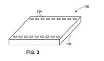
図3〜6は、図1の集積回路26などの集積回路の様々な実施形態を示す。具体的には、図3に示す第1の実施形態100では、貫設された2面TSV104を有する集積回路102が示されている。図1の貫通シリコンビア(TSV)30などの複数の貫通ビア104が、集積回路102の第1の面と第2の面の上に配置される。ある実施形態では、集積回路102の第1の面上のTSVの配置は、集積回路102の第2の面上のTSVの配置とは異なることに留意されたい。しかし、ある別の実施形態では、集積回路102の第1の側面と第2の側面の両方へのTSVの配置は概ね同じで良い。次に図4を参照すると、集積回路112上に部分アレイで配置された複数のTSV114を有する集積回路112の実施形態110が示されている。図5に示す実施形態120も、集積回路122の周囲に沿って配置されたTSV124の配置を示す。本明細書で用いる「部分アレイ」とは、ダイの全領域にTSVの二次元(2D)アレイをタイリングしないTSVのアレイを意味する。また、集積回路132上にフルアレイで配置された複数のTSV134を有する集積回路132の実施形態130が、図6に示されている。本明細書で用いる「フルアレイ」とは、ダイの全領域にTSVの2DアレイをタイリングするTSVのアレイを意味する。
3-6 illustrate various embodiments of an integrated circuit, such as
前述の通り、従来のパッケージ技術を用いて大型のセンサアレイを作製することは困難である。従って、大面積の検出器モジュールを構築することができるセンサ積層体の設計を開発することが望まれる。タイリングは、大面積センサモジュールの構築に関連する問題に対する魅力的な解決策をもたらすアプローチである。本発明によれば、センサ積層体40(図1を参照)などの個々のセンサモジュールをタイリングして、大面積の(X、Y)検出器モジュールを形成することによって例示的な検出器モジュールを構築しても良い。 As described above, it is difficult to produce a large sensor array using conventional package technology. Accordingly, it is desirable to develop a sensor stack design that can build a large area detector module. Tiling is an approach that provides an attractive solution to the problems associated with building large area sensor modules. In accordance with the present invention, an exemplary detector module by tiling individual sensor modules such as sensor stack 40 (see FIG. 1) to form a large area (X, Y) detector module. May be built.
本発明の一実施形態によれば、複数のセンサ積層体40が製造される。一例として、複数のセンサ積層体40を有するウェーハを製造しても良い。次いで、ウェーハはダイシングされ、個々のセンサ積層体が形成される。そして、個々のセンサ積層体が検査され、大面積の検出器モジュールを構築するために有利に使用される、良好であると判明したセンサ積層体が特定される。 According to one embodiment of the present invention, a plurality of sensor stacks 40 are manufactured. As an example, a wafer having a plurality of sensor stacks 40 may be manufactured. The wafer is then diced to form individual sensor stacks. Individual sensor stacks are then inspected to identify sensor stacks that have been found to be good for use in constructing large area detector modules.
次に図7を参照すると、例示的な検出器モジュールの一実施形態150が示されている。複数のセンサ積層体40(図1を参照)が基板152の第1の面上に定められたパターンで配置され、検出器モジュールを形成する。典型的に、基板152はシリコンなどの半導体材料、又はポリイミドなどの可撓性材料を含み得るが、同様の特性を有する別の種類の材料を用いても良い。基板152は更に、それに限定されないが個別電子部品などの別のコンポーネントを含んでも良い。
Referring now to FIG. 7, one
本発明の態様によれば、フリップチップはんだ接着工程を用いて高密度のタイリング可能な検出器積層体40を作製するために、複数のセンサ積層体40が基板152に接着される。より具体的には、フリップチップはんだ接着工程を用いることで、基板152上にセンサ積層体40を正確に配置し、極めて密なチップ間の間隔で極めて高密度の検出器モジュール150を形成することが可能になる。具体的には、本発明の態様により、センサ積層体40間の間隙が大幅に小さくなるように複数のセンサ積層体40を配置し得る。一例として、隣接して配置されたセンサ積層体40間の間隙は、約5μm〜約5200μmの範囲である。ある実施形態では、隣接して配置されたセンサ積層体40間の間隙は、約5μm〜約50μmの範囲である。
In accordance with an aspect of the present invention, a plurality of sensor stacks 40 are bonded to a
更に、プラグ接続可能な検出器モジュールを形成するため、基板152は検出器モジュール150の第2の面上に配置されたピンを有する。従って、結合手段154が基板152の第2の面上に配置され、この結合手段154は検出器モジュール150を別の電子素子に結合し易くする。そのため、複数の金属パッド156が、基板152の第2の面上に配置される。結合手段154は、金属パッド156の上に配置される。現在考えられている構成では、結合手段154は1つ又は複数の銅ピラーを含む。従って、銅ピラー154は各々の金属パッド156の上に配置される。複数のセンサ積層体40と、基板152の第2の面上に配置された結合手段154を有する基板152との組み合わせが、プラグ接続可能な検出器モジュール150を形成する。
Further, the
図8は、例示的な大面積の検出器モジュールの別の実施形態160を示す。図7を参照して前述した通り、複数のセンサ積層体40が定められたパターンで基板162の第1の面上に配置され、大面積の検出器モジュールを形成する。より具体的には、複数のセンサ積層体40は、基板162に接着されて極めて密なチップ間の間隔を有する極めて高密度の検出器モジュール160を形成するフリップチップはんだである。この場合も、結合手段164は基板162の第2の面上に配置され、結合手段164は検出器モジュール160を別の電子素子に結合し易くする。具体的には、複数の金属パッド166が基板162の第2の面上に配置される。結合手段164は金属パッド166上に配置される。また、図8の構成では、結合手段164はボールグリッドアレイ(BGA)を含む。一実施形態では、ボールグリッドアレイ164は、検出器モジュール160を次のレベルのパッケージにはんだ付けし易くする複数のはんだボールを含む。具体的には、ボールグリッドアレイ内のはんだボールを各々の金属パッド166上に配置して、パッケージ内の別の電子素子にはんだ付け可能な検出器モジュール160を形成しても良い。
FIG. 8 shows another
本発明の更に別の態様によれば、図7のプラグ接続可能な個々の検出器モジュール150をタイリングして、より大型のタイリング可能な検出器アレイを形成する。次に図9を参照すると、このような大面積検出器アレイの実施形態170が示されている。現在考えられている構成では、プラグ接続可能な複数の検出器モジュール150が定められたパターンで配置され、より大型の検出器アレイを形成する。具体的には、プラグ接続可能な個々の検出器モジュール150をマザーボード172にプラグ接続して、図9に示すような大型の(MxN)タイリング可能なアレイを作製しても良い。理解されるように、マザーボード172は、それらに限定されないが、高電圧のフィールドプログラマブルグリッドアレイ(FPGA)、電力調整回路、調整器、直流(DC)電源などの別のコンポーネントを含んでも良い。参照番号174は全体として、プラグ接続可能な検出器モジュール150をマザーボード172に結合し易くする、マザーボード172上に配置されたソケットを表している。また、図8の検出器モジュール160を用いて大型(MxN)のタイリング可能なアレイが形成される場合は、個々の検出器モジュール160はソケット174を介してマザーボード172にはんだ付けされることに留意されたい。大面積検出器アレイ170の設計によって各々の検出器モジュールが交換可能になり、それによって、不良の検出器モジュールを容易に取り外して交換できる現場交換可能ユニット(FRU)が作製される。
In accordance with yet another aspect of the present invention, the individual
また、本発明の更に別の態様によれば、デジタル及びアナログ信号がローカル処理されるタイリングされた大面積アレイを実現し得る。図10は、タイリングされた大面積検出器アレイの断面図180を示す。具体的には、図10に示す実施形態では、検出器モジュール160(図8を参照)などの複数のタイリング可能な検出器モジュールが定められたパターンで並置され、大面積検出器アレイを形成する。具体的には、複数の検出器モジュール160が第2の基板182上に配置され、図10に示すような大型(MxN)のタイリング可能なアレイが作製される。第2の基板182は、一般に共通システム基板と呼ばれる。
In accordance with yet another aspect of the present invention, a tiled large area array in which digital and analog signals are processed locally can be implemented. FIG. 10 shows a
図8を参照して前述したように、各々のタイリング可能な検出器モジュール160は、第1の基板162(図8を参照)上に配置された一連のタイリングされたセンサ積層体40から構成される。本発明の態様によれば、検出器モジュール160は付加的に、基板162の第2の面上に配置された処理回路を含む。処理回路は、制御電子素子184及び/又はその他のフロントエンド電子素子188を含む。制御電子素子184は、ある実施形態では、はんだバンプ186を使用することにより第1の基板162の第2の面に作用的に結合される。同様に、フロントエンド電子素子188も、はんだバンプ190を使用することにより、第1の基板162の第2の面に作用的に結合される。
As described above with reference to FIG. 8, each tiling-
制御電子素子184及び/又はフロントエンド電子素子188を含む処理回路は、信号のローカル処理及び制御機能を実行するために使用される。ある実施形態では、信号のローカル処理及び制御機能には、それらに限定されないがそれぞれのセンサ積層体の構成データの記憶、それぞれのセンサ積層体内のASICのプログラミング及び動作のタイミング及び制御、センサ積層体から受信した信号を処理するための振幅、可変利得制御、及びアナログ‐デジタル変換器、電圧調整器、電源デカップリング、並びに受信したデータを更なる処理のためにシステムバスにバッファするために、適宜の信号調整及び送信/受信手段が含まれる。送信/受信手段の性質は、電子素子(例えば低電圧差分信号処理(LVDS)、光通信、又は無線周波数(RF)である。
Processing circuitry including
更に、第2の基板182は標準的なプリント基板材料(例えばFR4)、シリコン基板、セラミック基板、剛性の支持基板を有する可撓性回路(例えばカプトン)、ガラス、又はその他の材料を含む。第2の基板182は平坦でも良く、又は別の形状のものでも良い。一例として、第2の基板182は湾曲していることで、腹部撮像用に使用する湾曲したアレイの形成を補助する。また、第2の基板182は、電力及び接地を提供するための、且つタイリング可能な個々のモジュール160に、又は個々のモジュール160から信号送信するための適宜の信号ルーティングを含む。更に、第2の基板182は、タイリング可能なモジュール160の物理的な支持体としての役割を果たし、タイリング可能なモジュール160間の相互接続は、コネクタを介して各々のタイリング可能なモジュール160に取り付けられる可撓性回路などの補助手段で達成されても良い。更に、はんだボール、スタッドバンプ、又はポストを用いて、タイリング可能なモジュール160を第2の基板182に接着しても良い。
Further, the
更に、タイリング可能な検出器アレイの平面図200が図11に示されている。具体的には、図11に示すように、タイリング可能な検出器モジュール160(図8を参照)などの複数のタイリング可能な検出器モジュールを、相互間の空隙を最小限にして(2xN)の構成でタイリングする。参照番号201及び202は、第1のタイリング可能な検出器モジュールと第2のタイリング可能な検出器モジュールとをそれぞれ表している。図11の実施形態では、図示のようにアレイ203の能動領域の上下でタイリング可能なモジュール201と202との間の信号接続を達成する。参照番号204は全体として信号接続を表している。また、フルにタイリングされた2Dアレイでは、図10の断面図に示すように信号接続の経路をアレイの真後ろにルーティングしても良い。
Further, a
図12は、センサモジュールの別の実施形態206の概略図である。図12に示す実施形態では、センサアレイ207はインターポーザ208を介して間接的に集積回路214に結合される。従って、センサアレイ207はインターポーザ208に作用的に結合される。前述のように、インターポーザ208は、1つの接続から別の接続へとルーティングする電気インターフェースである。ある実施形態では、インターポーザ208は剛性インターポーザを含み、一方、別のある実施形態では、インターポーザ208は可撓性インターポーザを含む。一例として、剛性インターポーザにはFR4材料が含まれ、一方、可撓性インターポーザにはポリイミドが含まれる。また、インターポーザ208には、セラミック材料又は有機材料が含まれていても良い。
FIG. 12 is a schematic diagram of another
現在考えられている構成では、センサアレイ207の第2の面はインターポーザ208の第1の面に結合され、センサアレイとインターポーザとの積層体を形成する。この結合を行い易くするため、第1の複数の接触パッド209がセンサアレイ207の第2の面上に配置され、この接触パッド209は、センサアレイ207をインターポーザ208に結合し易くするように構成される。また、第2の複数の接触パッド211がインターポーザ208の第1の面上に配置され、一方、第3の複数の接触パッド212がインターポーザ208の第2の面上に配置される。第2の複数の接触パッド211は、センサアレイ207のインターポーザ208への結合を補助する。具体的には、インターポーザ208の第1の面上に配置された第2の複数の接触パッド211は、一実施形態では、第2の複数の接触パッド211の配置がセンサアレイ207の第2の面上に配置された第1の複数の接触パッド209の配置と適合するようにインターポーザ208の第1の面上に配置される。また、金属線213は、第2の複数の接触パッド211を第3の複数の接触パッド212に作用的に結合し、この金属線は、電圧及び/又は電流をセンサアレイ207と集積回路214内の処理回路との間で伝送するように構成される。
In the presently contemplated configuration, the second surface of
更に、本発明の態様によれば、センサアレイ207は高温接着工程を用いてインターポーザ208に作用的に結合される。一実施形態では、センサアレイ207をインターポーザ208に作用的に結合するために、高温はんだフリップチップ接着工程が用いられる。そのため、センサアレイ207をインターポーザ208に作用的に結合し易くするように構成された接着手段210は、各々の第1の複数の接触パッド209、又は各々の第2の複数の接触パッド211上に配置される。前述の通り、接着手段210には、はんだボール、銅ピラー、又は液相拡散接合(TLP)材料が含まれていても良い。
Further in accordance with aspects of the present invention,
本発明の更に別の態様によれば、集積回路214はインターポーザ208の第2の面に作用的に結合される。この結合を達成するため、1つ又は複数の接触パッド215が集積回路214の第1の面上に配置される。具体的には、一実施形態では、集積回路214の第1の面上に配置される1つ又は複数の接触パッド215は、1つ又は複数の接触パッド215の配置がインターポーザ208の第2の面上に配置された第3の複数の接触パッド212の配置と適合するように集積回路214の第1の面上に配置される。また、結合手段216が、インターポーザ208の第2の面上の第3の複数の接触パッド212上に、又は集積回路214の第1の面上の1つ又は複数の接触パッド215上に配置される。結合手段216は、集積回路214をインターポーザ208に作用的に結合することを補助するように構成される。この場合も、接着手段216には、はんだボール、銅ピラー、又は液相拡散接合(TLP)材料が含まれる。更に、高温接着工程を用いて集積回路214をインターポーザ208に結合しても良い。
In accordance with yet another aspect of the present invention, integrated
更に、1組の金属パッド217がインターポーザ208の第2の面上に配置される。これらの金属パッド217は、センサアレイ207、インターポーザ208、及び集積回路214を含む積層体を基板220に結合することを補助する。具体的には、基板220はインターポーザ208の第2の面上に配置される。また、金属パッド219が基板220の第1の面上に配置される。結合手段218は、金属パッド217又は金属パッド219上に配置される。結合手段218は、基板220をインターポーザ208の第2の面に結合することを補助する。具体的には、本発明の態様によれば、基板220は、低温接着工程を用いてインターポーザ208の第2の面上に結合され、センサモジュール206を形成する。
In addition, a set of
次に図13を参照すると、タイリングされた大面積検出器アレイの断面図222が示されている。具体的には、図13に示す実施形態では、タイリング可能な複数の検出器モジュール223が定められたパターンで配置され、大面積検出器アレイが形成される。具体的には、図13に示すように、複数の検出器モジュール223が第2の基板226上に配置され、大型の(MxN)タイリング可能なアレイが作製される。第2の基板226は、一般に共通システム基板と呼ばれる。
Referring now to FIG. 13, a
各々のタイリング可能な検出器モジュール223は、第1の基板220上に配置された一連のタイリングされたセンサ積層体206から構成される(図12を参照)。本発明の態様によれば、検出器モジュール223は、付加的に基板220の第2の面上に配置された処理回路を含んでも良い。処理回路は、制御電子素子227及び/又はその他のフロントエンド電子素子229を含む。制御電子素子227は、ある実施形態では、はんだバンプ228を使用することにより、第1の基板220の第2の面に作用的に結合される。同様に、フロントエンド電子素子229も、はんだバンプ231を使用することにより、第1の基板220の第2の面に作用的に結合される。
Each tiling-
前述のように、制御電子素子227及び/又はフロントエンド電子素子229を含む処理回路は、信号のローカル処理及び制御機能を実行するために使用される。また、第2の基板226は、標準的なプリント基板材料(例えばFR4)、シリコン基板、セラミック基板、剛性の支持基板を有する可撓性回路(例えばカプトン)、ガラス、又はその他の材料を含む。第2の基板226は平坦でも良く、又は別の形状のものでも良い。更に、結合手段225を用いて、タイリング可能な検出器モジュール223を第2の基板226上に接着する。結合手段225には、はんだボール、スタッドバンプ、又はポストが含まれる。参照番号224は全体として、基板220の第2の面上に配置される金属パッドを表している。タイリング可能な複数の検出器モジュール223を第2の基板226に結合することを補助するため、結合手段225をこれらの金属パッド224上に配置しても良い。本発明の態様によれば、タイリング可能な複数の検出器モジュール223は、低温接着工程を用いて第2の基板226に結合される。
As described above, processing circuitry including
更に、図2に示すように、インターポーザを使用してセンサアレイを間接的に相互接続相に結合しても良い。図14は、図2のセンサモジュール60を形成する方法の概略図230を示している。図14(a)に示すように、この方法には、図2のインターポーザ64のようなインターポーザ232を設けるステップが含まれる。インターポーザ232は、第1の面234と第2の面236とを有する。現在考えられている構成では、インターポーザ232は有機インターポーザが含まれる。同様の特性を有する別の材料を用いてインターポーザを形成しても良いことに留意されたい。更に、本発明の態様によれば、インターポーザ232は1つ又は複数の貫通ビア238を含み、1つ又は複数の貫通ビア238にはセンサアレイの性能を最適化するように構成されたエポキシが充填される。また、第1組の接触パッド240がインターポーザ232の第1の面234に沿って貫通ビア238上に配置され、一方、第2組の接触パッド242はインターポーザ232の第2の面236に沿って貫通ビア238上に配置される。第1組の接触パッド240は、センサアレイをインターポーザ232の第1の面234に結合するために役立ち、一方、第2組の接触パッド242は、インターポーザ232、又はASICなどの別の電子素子の第2の面に結合するために役立つ。
Further, as shown in FIG. 2, the sensor array may be indirectly coupled to the interconnect phase using an interposer. FIG. 14 shows a schematic diagram 230 of a method of forming the
また、第1の補強材244がインターポーザ232の第2の面236上に配置される。また、一実施形態では、第1の補強材をインターポーザ232の第2の面236の一部に接着する。一例として、一実施形態では、第1の補強材244をインターポーザ232の第2の面236の周囲に沿って取り付ける。第1の補強材244は、インターポーザ232の剛性と平坦さを保つために、インターポーザ232を支持するように構成される。ステンレス鋼又はセラミック部材を用いて第1の補強材244を形成しても良い。ステンレス鋼のCTE値は11ppm/℃であり、これは基板のCTE値と概ね一致するので、第1の補強材244を形成するためにステンレス鋼が使用されることに留意されたい。更に、第1の補強材244は、リング形、ボックス形、円形、方形などの形状のもので良い。
A first reinforcing
その後、図14(b)に示すように、センサ層246が設けられる。具体的には、センサ層246はインターポーザ232の第1の面234上に配置され、センサアレイとインターポーザとの積層体256を形成する。このセンサ層246は、センサアレイと支持層250とを含む。また、センサアレイ248の厚さは、約50μm〜約3000μmの範囲である。ある実施形態では、支持層250はセンサアレイ248を支持するように構成される。更に、センサアレイ248が超音波トランスデューサアレイを含む場合は、超音波反射板として機能するように支持層250を構成しても良い。一例として、超音波プローブのように、支持層250は炭化タングステン(WC)によって形成され、超音波エネルギを外向き方向に推進する役割を果たす。
Thereafter, as shown in FIG. 14B, a
更に、図14(b)に示されるように、センサアレイ248をダイシングして、センサアレイとインターポーザとの積層体256を別の電子素子に取り付ける前に、複数のセンサ素子252を形成しても良い。参照番号254は、全体として切り口を表している。センサアレイとインターポーザとの積層体256を形成した後であるが、センサアレイとインターポーザとの積層体256を別の電子素子に結合する前に、センサアレイ248をダイシングしてセンサ素子252を形成することで、ASICなどの敏感な電子素子が激しい振動に晒され、ダイシング工程中に粉塵が発生することが回避される。また、インターポーザ232を使用することで、センサアレイ形成工程がセンサアレイとインターポーザとの積層体256を、ASICに取り付けるために用いられるより清浄なマイクロエレクトロニクス取り付け工程と分離することが可能になる。
Further, as shown in FIG. 14B, a plurality of
センサアレイ248が超音波トランスデューサを含む場合、一実施形態では、超音波トランスデューサアレイ248はcMUTを含んでも良いことに留意されたい。このような場合、複数のセンサ素子を形成するための図14(b)のダイシングステップを省いても良い。
Note that if the
更に、図14(c)に示すように、第2の補強材258がインターポーザ232の第1の面234上に配置される。第2の補強材258は、ステンレス鋼又はセラミック材料を用いて形成される。具体的には、第2の補強材258は高弾性率の材料を用いて形成される。更に、第2の補強材258は、典型的には弾性率が比較的低い材料を用いて形成されるインターポーザ232を支持するように構成される。また、第2の補強材258は、第1の面234上のインターポーザ232の構造的に強固な支持体を提供することによって、スクリーン印刷やその他の工程を可能にする平坦な遮られない表面を備えるように構成される。一実施形態では、第2の補強材258をインターポーザ232の第1の面234に取り付けるために、低温工程が用いられる。また、図14(d)に示すように、第1の補強材244は切断され、その結果、接点242への微細ピッチの低温エポキシ堆積層をステンシル印刷することを可能にするセンサ積層体の構成が得られる。この場合、センサ層246の製造中に構造を支えるために第1の補強材244が用いられる。しかし、接触パッド242上で別の動作を実行できるようにするため、第1の補強材244は次いで除去される。更に、図14(e)に示すように、センサ積層体260が形成される。このセンサ積層体260は、1つ又は複数のASICを含み得る相互接続層の第1の面に取り付けられる。
Further, as shown in FIG. 14C, the second reinforcing
図15は、図2のセンサモジュール60などのセンサモジュールの一実施形態270を示す。図15では、センサ積層体(図14を参照)は相互接続層272に作用的に結合される。前述のように、相互接続層272は、再配線層274と、ASICなどの集積回路276を含む。具体的には、センサ積層体246を相互接続層272に結合するため、一実施形態では、複数のスタッドバンプ278を第2組の金属パッド242(図14を参照)上に配置する。ある実施形態では、スタッドバンプ278には金(Au)のスタッドバンプが含まれる。金のスタッドバンプを第2組の金属パッド242に取り付けるために、エポキシ塗布工程が用いられる。この金のスタッドバンプ278は、センサ積層体246と相互接続層272との間の均一の高さを保つことを補助する。低温工程を用いてセンサ積層体272を相互接続層272に取り付けて、センサモジュール270を形成しても良い。
FIG. 15 illustrates one
第2の補強材258をインターポーザ232の第1の面234に取り付ける工程と、センサアレイとインターポーザとの積層体256を相互接続層232に取り付ける工程の両方の工程とも比較的低温(例えば100℃未満)で実行されるため、センサモジュール270は損傷を受けない。例えば、超音波トランスデューサ材料を低温で処理することは、材料の圧電特性を確保するために材料をリポールする必要がないことを意味する。また、放射線検出器の場合、材料は高い抵抗性と良好な電荷収集効率を保つ。更に、ある種のセンサモジュールは温度に敏感である。具体的には、一般に使用されているチタン酸ジルコン酸鉛(PZT)は、温度が特性温度Tc、すなわちキュリー温度に近付くとその圧電特性を失う。1つの共通式PZT−5Hの場合、キュリー温度は190℃である。T≪Tcで相互接続層を処理できることは、材料の圧電作用を再生するために必要とされる追加の処理ステップが回避されるので有利である。理解されるように、この工程はリポールである。
Both the process of attaching the
本発明の態様によれば、図15の金のスタッドバンプ278の代わりに、又はこれと組み合わせて、銅ピラーを用いてセンサ積層体246を相互接続層272に作用的に結合しても良い。図16は、図2のセンサモジュール60などのセンサモジュールの別の実施形態280を示している。具体的には、図16では、センサモジュール(図15を参照)は銅ピラー282を使用して相互接続層272(図15を参照)などの相互接続層に作用的に結合される。従って、センサ積層体246を相互接続層272に結合することを補助するため、銅ピラー282が第2組の金属パッド242上に配置される。
In accordance with an aspect of the present invention, the
本発明の態様によれば、上述の検出器モジュールの様々な実施形態を超音波撮像システムなどの医用撮像システムに使用できる。図17は、超音波撮像システム290の実施形態のブロック図である。更に、超音波撮像システム290は収集サブシステム292と処理サブシステム294とを含むものとして図示されている。収集サブシステム292は、トランスデューサアセンブリ306を含んでも良い。また、収集サブシステム292は、送信/受信(T/R)切り換え回路308、送信機310、受信機312、及びビームフォーマ314を含む。
In accordance with aspects of the present invention, various embodiments of the detector modules described above can be used in medical imaging systems such as ultrasound imaging systems. FIG. 17 is a block diagram of an embodiment of an
一実施形態では、トランスデューサアセンブリ306を超音波プローブなどの画像収集装置内に配置する。また、ある実施形態では、トランスデューサアセンブリ306は典型的に、例えば一次元又は二次元トランスデューサアレイなどのトランスデューサアレイを形成するために間隔を隔てて配置される複数のトランスデューサ素子(図示せず)を含む。現在考えられている構成では、検出器モジュール150、160、170、及び180をトランスデューサアセンブリ306内で使用しても良い。また、トランスデューサアセンブリ306は、トランスデューサアレイを、それに限定されないがケーブルアセンブリ又は関連する電子素子などの外部装置(図示せず)に作用的に結合し易くするように構成された相互接続構造(図示せず)を含む。相互接続構造は、トランスデューサアレイをT/R切り換え回路308に結合するように構成される。
In one embodiment, the
処理サブシステム294は、制御プロセッサ316、復調器318、撮像モードプロセッサ320、スキャンコンバータ322、及びディスプレープロセッサ324を含む。ディスプレープロセッサ324は更に、画像を表示するためにディスプレーモニタ300に結合される。ユーザーインターフェース302は、制御プロセッサ316及びディスプレー300と相互作用する。制御プロセッサ316を、ウェブサーバ328及びリモート接続インターフェース330を含むリモート接続サブシステム326に結合しても良い。処理サブシステム294を更に、超音波画像データを受けるように構成されたデータリポジトリ298に結合しても良い。データリポジトリ298は、画像ワークステーション334と相互作用する。
The
前述のコンポーネントは、デジタル信号プロセッサを有する回路板などの専用ハードウェア素子でも良く、又は商用オフザシェルフパーソナルコンピュータ(PC)などの汎用コンピュータ又はプロセッサで実行されるソフトウェアであっても良い。本発明の様々な実施形態に応じて、様々なコンポーネントを組み合わせたり分離したりしても良い。従って、超音波撮像システムは例示的に提示されたものであり、本発明は特定のシステム構成に決して限定されないことが当業者には理解されよう。 The aforementioned components may be dedicated hardware elements such as circuit boards with digital signal processors, or may be software executed on a general purpose computer or processor such as a commercial off-the-shelf personal computer (PC). Various components may be combined or separated according to various embodiments of the present invention. Accordingly, those skilled in the art will appreciate that the ultrasound imaging system is presented by way of example and that the present invention is in no way limited to a particular system configuration.
収集サブシステム292で、トランスデューサアセンブリ306は患者332と接触する。トランスデューサアセンブリ306は、送信/受信(T/R)切り換え回路308に結合される。また、T/R切り換え回路308は、送信機310の出力及び受信機312の入力と作用に関連する。受信機312の出力は、ビームフォーマ314の入力である。また、ビームフォーマ314は更に、送信機310の入力、及び復調器318の入力に結合される。ビームフォーマ314はまた、図17に示すように制御プロセッサ316に作用的に結合される。
At the
処理サブシステム294で、復調器318の出力は撮像モードプロセッサ320の入力と作用的に関連する。また、制御プロセッサ316は撮像モードプロセッサ320、スキャンコンバータ322、及びディスプレープロセッサ324と相互作用する。撮像モードプロセッサ320の出力は、スキャンコンバータ322の入力に結合される。また、スキャンコンバータ322の出力は、ディスプレープロセッサ324の入力に作用的に結合される。ディスプレープロセッサ324の出力は、ディスプレー300に結合される。
In
超音波システム290は、超音波エネルギを患者332に伝送し、患者332からの後方散乱超音波信号を受信し、且つ処理して画像を生成し、表示する。超音波エネルギの透過ビームを生成するため、制御プロセッサ316はコマンドデータをビームフォーマ314に送り、送信パラメータを作成して、所望の操舵角でトランスデューサアセンブリ306の表面のあるポイントから発する所望の形状のビームを生成する。送信パラメータは、ビームフォーマ314から送信機310に送られる。送信機310は、送信パラメータを利用して、T/R切り換え回路308を経てトランスデューサアセンブリ306に送られる予定の送信信号を適切にエンコードする。送信信号は、相互にあるレベル及び位相に設定され、トランスデューサアセンブリ306の個々のトランスデューサ素子に提供される。送信信号はトランスデューサ素子を励起して、同じ位相及びレベル関係で超音波を投射させる。その結果、トランスデューサアセンブリ306が、例えば超音波ゲルを用いて患者332に音響結合されると、走査線に沿って超音波エネルギの透過ビームが患者332の体内に形成される。この工程は電子スキャンとして知られている。
The
一実施形態では、トランスデューサアセンブリ306は2方向トランスデューサである。超音波が患者332の体内に透過されると、超音波は患者332の組織及び血液サンプルから後方散乱する。トランスデューサアセンブリ306は、後方散乱波がそこから戻るまでの距離、及びトランスデューサアセンブリ306の表面に対する角度に応じて異なるタイミングで後方散乱波を受信する。トランスデューサ素子は、後方散乱波からの超音波エネルギを電気信号に変換する。
In one embodiment,
次いで、電気信号は、T/R切り換え回路308を経て受信機312に送られる。受信機312は、受信した信号を増幅し、且つデジタル化し、利得補償などの別の機能を提供する。異なるタイミングで各々のトランスデューサ素子によって受信された後方散乱波に対応するデジタル化された受信信号は、組織を通る音響経路の長さによって左右される。また、デジタル化された受信信号は後方散乱波の振幅及び位相の情報を保存する。
The electrical signal is then sent to the
デジタル化された信号はビームフォーマ314に送られる。制御プロセッサ316は、コマンドデータをビームフォーマ314に送る。ビームフォーマ314はコマンドデータを利用して、典型的には走査線に沿って透過された以前の超音波ビームのポイントと操舵角とに対応する操舵角でトランスデューサアセンブリ306の表面上のポイントから発された受信ビームを形成する。ビームフォーマ314は、制御プロセッサ316からのコマンドデータの命令に従って時間遅延及び集束を行うことによって、適宜の受信信号で動作して、患者322の体内の走査線に沿ったサンプル値に対応する受信ビーム信号を生成する。受信ビーム信号を生成するため、様々なトランスデューサ素子から受信した信号の位相、振幅、及びタイミング情報が利用される。
The digitized signal is sent to the
受信ビーム信号は処理サブシステム294に送られる。復調器318は受信ビーム信号を復調して、走査線に沿ったサンプル値に対応する一対のI及びQ復調データ値を生成する。復調は、受信ビーム信号の位相及び振幅を基準周波数と比較することによって達成される。I及びQ復調データ値は、受信信号の位相及び振幅情報を保存する。
The receive beam signal is sent to the
復調データは撮像モードプロセッサ320に伝送される。撮像モードプロセッサ320はパラメータ評価技術を用いて、復調データから走査シーケンスフォーマットで撮像パラメータ値を生成する。撮像パラメータには、例えばBモード、カラー音速モード、スペクトルドップラーモード、及び組織速度撮像モードなどの可能な様々な撮像モードに対応するパラメータが含まれていても良い。撮像パラメータ値はスキャンコンバータ322に送られる。スキャンコンバータ322は、走査シーケンスフォーマットからディスプレーフォーマットへの変換を行うことによって、パラメータデータを処理する。変換には、パラメータデータに補間動作を行ってディスプレーフォーマットでディスプレー・ピクセルデータを生成することも含まれる。
The demodulated data is transmitted to the
走査変換ピクセルデータはディスプレープロセッサ324に送られ、これは走査変換ピクセルデータにいずれかの最終的又は暫定的なフィルタリングを行って、走査変換ピクセルデータにグレースケール又はカラーを指定し、且つディスプレー300に表示するためにデジタルピクセルデータをアナログデータに変換する。ディスプレー300に表示されたデータに基づいて、ユーザーが超音波撮像システム290とインターフェース連絡できるように、ユーザーインターフェース302が制御プロセッサ316に結合される。
The scan converted pixel data is sent to the
更に、撮像システム290、収集サブシステム292、及び/又は処理サブシステム294によって実行し得るような前述の実施例、説明内容及び工程ステップを、汎用又は専用コンピュータなどのプロセッサベースシステムで適宜のコードにより実施しても良い。更に、本発明の異なる実装形態が、本明細書に記載のステップの一部又は全部を異なる順序で、又は概ね同時に、すなわち並行して実行しても良いことにも留意されたい。更に、諸機能は、それらに限定されないがC++又はJava(商標)を含む多様なプログラミング言語で実装される。このようなコードは、プロセッサベースのシステムによりアクセスして保存されたコードを実行し得る、データレジストリチップ、ローカル又はリモートハードディスク、光ディスク(すなわちCD又はDVD)、メモリ、又はその他の媒体などの1つ又は複数の有形の機械読取り可能媒体に保存され、又は格納されるように構成される。有形媒体は命令がプリントされた紙、又はその他の適宜の媒体であっても良いことに留意されたい。例えば、命令を紙又はその他の媒体の光学走査により電子的に取り込み、次いでコンパイル、解読、又は必要ならば適宜の方法で処理し、その後データレジストリ298又はメモリに保存する。
Further, the foregoing embodiments, descriptions and process steps as may be performed by
上述の検出器モジュール形成方法、及び検出器モジュールの様々な実施形態は、二次元高密度のタイリング可能なセンサアレイを形成する能力を劇的に高める。具体的には、ASIC内に貫通シリコンビア(TSV)を使用することで、電力信号、接地信号、アナログ信号、及び/又はデジタル信号をダイの真下にルーティングすることが可能になる。また、上述の方法によって、高温接着工程を用いてASICの上部にセンサアレイを接着し、センサ積層体を形成することが可能になる。また、貫設されたTSVを有するASICの上部にセンサを直接積層することで、フリップチップダイと同様に取り扱い可能なタイリング可能な素子を形成することが可能になる。 The above-described detector module formation methods and various embodiments of detector modules dramatically increase the ability to form a two-dimensional high density tiling-capable sensor array. Specifically, using through silicon vias (TSVs) within the ASIC allows power signals, ground signals, analog signals, and / or digital signals to be routed directly under the die. Further, by the above-described method, it is possible to bond the sensor array to the upper part of the ASIC using a high temperature bonding process to form a sensor laminate. In addition, by directly stacking the sensor on the top of the ASIC having the TSVs that are provided through, it is possible to form a tiling-able element that can be handled in the same manner as a flip chip die.
更に、複数のセンサ積層体は、基板に接着してチップ間の間隔が極めて密な超高密度検出器モジュールを製造するためのフリップチップはんだであっても良い。また、これらの検出器モジュールをプラグ接続可能な検出器モジュールとして形成することができる。そしてこれらのプラグ接続可能な検出器モジュールを、より大型のタイリング可能なアレイを作製するために使用できる。このパッケージ概念により、積層体全体が取り付けられる場合に相互接続がリフローしないように高密度検出器アレイを作製可能になる。また、検出器モジュールを基板にプラグ接続するか、又ははんだ付けすることによって、FRU検出器モジュールを形成可能である。また、この方法はセンサ積層体をインターポーザ上に作製し、この積層体をASIC上に結合するのに役立つ。更に、携帯システムで使用する輪郭が極めて小さい小型パッケージを作製するためにこのパッケージ概念を利用できる。 Further, the plurality of sensor stacks may be flip chip solder for manufacturing an ultra-high density detector module that is bonded to a substrate and has a very close spacing between chips. Moreover, these detector modules can be formed as detector modules that can be plugged. These pluggable detector modules can then be used to make larger tilingable arrays. This package concept allows a high density detector array to be made so that the interconnect does not reflow when the entire stack is attached. Also, the FRU detector module can be formed by plugging or soldering the detector module to the substrate. This method also helps to make the sensor stack on the interposer and bond the stack onto the ASIC. In addition, this package concept can be used to produce small packages with very small profiles for use in portable systems.
本明細書では、本発明のある特定の特徴を図示し、記載したが、当業者には多くの修正や変更が考えられよう。従って、このような修正や変更は、本発明の真の趣旨に含まれることを意図するものである。 While certain features of the invention have been illustrated and described herein, many modifications and changes will occur to those skilled in the art. Accordingly, such modifications and changes are intended to be included in the true spirit of the present invention.
10 センサモジュールの形成方法のフローチャート
12 センサアレイを配置するステップ
16 センサアレイの第1の面
18 センサアレイの第2の面
20 接触パッド
22 相互接続層
24 再配線層
26 集積回路
28 接触パッド
30 貫通ビア
32 接触パッド
34 金属線
36 接着手段
38 センサ積層体を形成するステップ
40 センサ積層体
42 基板
44 金属パッド
46 はんだバンプ
48 金属パッド
50 形成されたセンサモジュールを示すステップ
52 センサモジュール
60 センサモジュール
62 センサアレイ
63 センサアレイとインターポーザとの積層体
64 インターポーザ
66 接触パッド
68 相互接続層
70 再配線層
72 集積回路
74 接触パッド
76 貫通ビア
78 接触パッド
80 金属線
81 センサ積層体
82 接着手段
84 基板
86 金属パッド
88 はんだバンプ
90 金属パッド
100 貫通シリコンビア(TSV)を有する集積回路
102 集積回路
104 TSV
110 貫通シリコンビア(TSV)を有する集積回路
112 集積回路
114 TSV
120 貫通シリコンビア(TSV)を有する集積回路
122 集積回路
124 TSV
130 貫通シリコンビア(TSV)を有する集積回路
132 集積回路
134 TSV
150 検出器モジュール
152 基板
154 結合手段
156 金属パッド
160 検出器モジュール
162 基板
164 結合手段
166 金属パッド
170 大面積検出器アレイ
172 マザーボード
174 ソケット
180 大面積検出器アレイ
182 共通システム基板
184 制御電子素子
186 はんだバンプ
188 フロントエンド電子素子
190 はんだバンプ
200 大面積検出器アレイの平面図
201 第1のタイリング可能な検出器モジュール
202 第2のタイリング可能な検出器モジュール
203 能動アレイ
204 信号接続
206 センサ積層体
207 センサアレイ
208 インターポーザ
209 接触パッド
210 はんだバンプ
211 接触パッド
212 接触パッド
213 金属線
214 集積回路
215 接触パッド
216 はんだバンプ
217 金属パッド
218 はんだバンプ
219 金属パッド
220 基板
222 大面積検出器アレイ
223 検出器モジュール
224 接触パッド
225 はんだバンプ
226 共通システム基板
227 制御電子素子
228 はんだバンプ
229 フロントエンド電子素子
230 インターポーザを有するセンサモジュールを形成する方法
231 はんだバンプ
232 インターポーザ
234 インターポーザの第1の面
236 インターポーザの第2の面
238 貫通ビア
240 接触パッド
242 接触パッド
244 第1の補強材
246 センサ層
248 センサアレイ
250 支持層
252 センサ素子
254 切り口
256 センサアレイとインターポーザとの積層体
258 第2の補強材
260 センサ積層体
270 検出器モジュール
272 相互接続層
274 再配線層
276 集積回路
278 スタッドバンプ
280 検出器モジュール
282 銅ピラー
290 医用撮像システム
292 収集サブシステム
294 処理サブシステム
298 データリポジトリ
300 ディスプレー
302 ユーザーインターフェース
306 トランスデューサアセンブリ
308 送信/受信(T/R)切り換え回路
310 送信機
312 受信機
314 ビームフォーマ
316 制御プロセッサ
318 復調器
320 撮像モードプロセッサ
322 スキャンコンバータ
324 ディスプレープロセッサ
326 リモート接続サブシステム
328 ウェブサーバ
330 インターフェース
332 患者
334 画像ワークステーション
DESCRIPTION OF
110 Integrated Circuit with Through Silicon Via (TSV) 112
120 Integrated Circuit with Through Silicon Via (TSV) 122
130 Integrated Circuit with Through Silicon Via (TSV) 132
150 detector module 152 substrate 154 coupling means 156 metal pad 160 detector module 162 substrate 164 coupling means 166 metal pad 170 large area detector array 172 motherboard 174 socket 180 large area detector array 182 common system substrate 184 control electronics 186 solder Bump 188 Front-end electronics 190 Solder bump 200 Plan view of large area detector array 201 First tiling-capable detector module 202 Second tiling-capable detector module 203 Active array 204 Signal connection 206 Sensor stack 207 Sensor array 208 Interposer 209 Contact pad 210 Solder bump 211 Contact pad 212 Contact pad 213 Metal wire 214 Integrated circuit 215 Contact pad 2 16 Solder bump 217 Metal pad 218 Solder bump 219 Metal pad 220 Substrate 222 Large area detector array 223 Detector module 224 Contact pad 225 Solder bump 226 Common system substrate 227 Control electronics 228 Solder bump 229 Front end electronics 230 With interposer Method of Forming Sensor Module 231 Solder Bump 232 Interposer 234 Interposer First Surface 236 Interposer Second Surface 238 Through Via 240 Contact Pad 242 Contact Pad 244 First Stiffener 246 Sensor Layer 248 Sensor Array 250 Support Layer 252 Sensor element 254 Cut end 256 Laminated body of sensor array and interposer 258 Second reinforcing material 260 Sensor laminated body 270 Detector Module 272 Interconnect layer 274 Redistribution layer 276 Integrated circuit 278 Stud bump 280 Detector module 282 Copper pillar 290 Medical imaging system 292 Acquisition subsystem 294 Processing subsystem 298 Data repository 300 Display 302 User interface 306 Transducer assembly 308 Transmit / receive ( T / R) switching circuit 310 transmitter 312 receiver 314 beamformer 316 control processor 318 demodulator 320 imaging mode processor 322 scan converter 324 display processor 326 remote connection subsystem 328 web server 330 interface 332 patient 334 image workstation
Claims (9)
検出器モジュールを形成するステップであって、
第1の面と第2の面とを有し、センサアレイの第2の面上に配置された第1の複数の接触パッドを備える前記センサアレイを設けるステップと、
第1の面と第2の面とを有し、再配線層の第1の面上に配置された第2の複数の接触パッドを備える前記再配線層と、
複数の貫通ビアが貫設されている集積回路であって、該集積回路の第1の面が前記再配線層の第2の面に作用的に結合され、前記集積回路が、前記集積回路の前記第1の面と第2の面においてパターン配列で配置された複数の貫通ビアを有し、前記第1の面の前記貫通ビアのパターン配列が、前記第2の面の前記貫通ビアのパターン配列と異なっている、前記集積回路と、を備える相互接続層上にセンサアレイを配置するステップであって、
前記センサアレイの前記第2の面上の第1の複数の接触パッドが、前記再配線層の前記第1の面上の第2の複数の接触パッドと位置合わせされるように、前記センサアレイを前記相互接続層上に配置するステップと、
前記センサアレイの前記第2の面上の第1の複数の接触パッドを、前記再配線層の前記第1の面上の第2の複数の接触パッドに作用的に結合して、センサ積層体を形成するステップと、
前記センサ積層体を第1の基板に結合して、前記検出器モジュールを形成するステップと、
第2の基板上に複数の前記検出器モジュールをタイリングして、前記タイリング可能な検出器アレイを形成するステップとを含む方法。 In a method of forming a tileable detector array,
Forming a detector module comprising:
Providing the sensor array comprising a first plurality of contact pads having a first surface and a second surface and disposed on the second surface of the sensor array;
The redistribution layer having a first surface and a second surface, and comprising a second plurality of contact pads disposed on the first surface of the redistribution layer;
An integrated circuit having a plurality of through vias, wherein the first surface of the integrated circuit is operatively coupled to the second surface of the redistribution layer; A plurality of through vias arranged in a pattern arrangement on the first surface and the second surface, wherein the pattern arrangement of the through vias on the first surface is a pattern of the through vias on the second surface; Disposing a sensor array on an interconnect layer comprising an integrated circuit different from the array comprising:
The sensor array such that a first plurality of contact pads on the second surface of the sensor array are aligned with a second plurality of contact pads on the first surface of the redistribution layer. Placing on the interconnect layer;
A first plurality of contact pads on the second surface of the sensor array are operatively coupled to a second plurality of contact pads on the first surface of the redistribution layer to provide a sensor stack. Forming a step;
Bonding the sensor stack to a first substrate to form the detector module;
Tiling a plurality of the detector modules on a second substrate to form the tileable detector array.
第1の面と第2の面とを有する第1の基板(162)と、
前記第1の基板(162)の第1の面上に配置された複数の検出器モジュール(160)であって、複数の検出器モジュール(160)の各々が、
第1の面と第2の面とを有していて、第1の複数の接触パッド(20)がセンサアレイ(14)の第2の面上に配置されている前記センサアレイ(14)と、
相互接続層(22)であって、
第1の面と第2の面とを有し、再配線層(24)の前記第1の面上に配置された第2の複数の接触パッド(28)を備える前記再配線層(24)と、
集積回路(26)の第1の面が前記再配線層(24)の前記第2の面に作用的に結合され、複数の貫通ビア(30)が貫設されており、前記集積回路が、前記集積回路の前記第1の面と第2の面においてパターン配列で配置された複数の貫通ビアを有し、前記第1の面の前記貫通ビアのパターン配列が、前記第2の面の前記貫通ビアのパターン配列と異なっている前記集積回路(26)と、を備え、
前記センサアレイ(14)の前記第2の面上の前記第1の複数の接触パッド(20)が、前記再配線層(24)の前記第1の面上の前記第2の複数の接触パッド(28)と位置合わせされるように、前記センサアレイ(14)が前記相互接続層(22)上に配置され、前記センサアレイ(14)の前記第2の面上の前記第1の複数の接触パッド(20)が、前記再配線層(24)の前記第2の複数の接触パッド(28)に作用的に結合され、且つ、
前記集積回路(26)の第2の面上に配置された結合手段(154)を備える前記相互接続層(22)と、を備える前記複数の検出器モジュール(160)とを備え、
前記複数の検出器モジュール(160)が、前記集積回路(26)の前記第2の面上に配置された前記結合手段(154)を介して前記第1の基板(162)の前記第1の面に結合される、タイリング可能な検出器アレイ。 In the tilingable detector array (170),
A first substrate (162) having a first surface and a second surface;
A plurality of detector modules (160) disposed on a first surface of the first substrate (162), each of the plurality of detector modules (160) being
The sensor array (14) having a first surface and a second surface, wherein the first plurality of contact pads (20) are disposed on the second surface of the sensor array (14); ,
An interconnect layer (22),
The redistribution layer (24) comprising a second plurality of contact pads (28) having a first surface and a second surface and disposed on the first surface of the redistribution layer (24). When,
A first surface of the integrated circuit (26) is operatively coupled to the second surface of the redistribution layer (24), and a plurality of through vias (30) are provided through the integrated circuit. A plurality of through vias arranged in a pattern arrangement on the first surface and the second surface of the integrated circuit, wherein the pattern arrangement of the through vias on the first surface is the second surface of the integrated circuit; The integrated circuit (26) different from the pattern arrangement of through vias , and
The first plurality of contact pads (20) on the second surface of the sensor array (14) is the second plurality of contact pads on the first surface of the redistribution layer (24). (28), the sensor array (14) is disposed on the interconnect layer (22), and the first plurality of the first array on the second surface of the sensor array (14). A contact pad (20) is operatively coupled to the second plurality of contact pads (28) of the redistribution layer (24); and
A plurality of detector modules (160) comprising: an interconnection layer (22) comprising coupling means (154) disposed on a second surface of the integrated circuit (26);
The plurality of detector modules (160) are arranged on the first surface of the first substrate (162) via the coupling means (154) disposed on the second surface of the integrated circuit (26). A tilingable detector array coupled to a surface.
9. The tilingable detector array of claim 7 or 8 , further comprising a second substrate operatively coupled to the one or more pluggable detector modules to form a field replaceable unit. (170).
Applications Claiming Priority (2)
| Application Number | Priority Date | Filing Date | Title |
|---|---|---|---|
| US12/956,194 | 2010-11-30 | ||
| US12/956,194 US8659148B2 (en) | 2010-11-30 | 2010-11-30 | Tileable sensor array |
Publications (3)
| Publication Number | Publication Date |
|---|---|
| JP2012118060A JP2012118060A (en) | 2012-06-21 |
| JP2012118060A5 JP2012118060A5 (en) | 2014-12-25 |
| JP5955537B2 true JP5955537B2 (en) | 2016-07-20 |
Family
ID=46052454
Family Applications (1)
| Application Number | Title | Priority Date | Filing Date |
|---|---|---|---|
| JP2011252145A Active JP5955537B2 (en) | 2010-11-30 | 2011-11-18 | Tileable sensor array |
Country Status (3)
| Country | Link |
|---|---|
| US (1) | US8659148B2 (en) |
| JP (1) | JP5955537B2 (en) |
| FR (1) | FR2968124A1 (en) |
Families Citing this family (66)
| Publication number | Priority date | Publication date | Assignee | Title |
|---|---|---|---|---|
| US9177926B2 (en) | 2011-12-30 | 2015-11-03 | Deca Technologies Inc | Semiconductor device and method comprising thickened redistribution layers |
| US10373870B2 (en) | 2010-02-16 | 2019-08-06 | Deca Technologies Inc. | Semiconductor device and method of packaging |
| US9576919B2 (en) | 2011-12-30 | 2017-02-21 | Deca Technologies Inc. | Semiconductor device and method comprising redistribution layers |
| US8922021B2 (en) | 2011-12-30 | 2014-12-30 | Deca Technologies Inc. | Die up fully molded fan-out wafer level packaging |
| DE102011012989B4 (en) * | 2011-03-03 | 2019-05-02 | Ketek Gmbh | Sensor head for an x-ray detector |
| TW201320266A (en) * | 2011-11-11 | 2013-05-16 | Xintec Inc | Semiconductor package and method of fabricating the same |
| US10050004B2 (en) | 2015-11-20 | 2018-08-14 | Deca Technologies Inc. | Fully molded peripheral package on package device |
| US10672624B2 (en) | 2011-12-30 | 2020-06-02 | Deca Technologies Inc. | Method of making fully molded peripheral package on package device |
| WO2013102146A1 (en) | 2011-12-30 | 2013-07-04 | Deca Technologies, Inc. | Die up fully molded fan-out wafer level packaging |
| US9613830B2 (en) | 2011-12-30 | 2017-04-04 | Deca Technologies Inc. | Fully molded peripheral package on package device |
| US9831170B2 (en) | 2011-12-30 | 2017-11-28 | Deca Technologies, Inc. | Fully molded miniaturized semiconductor module |
| US20140005527A1 (en) * | 2012-06-29 | 2014-01-02 | General Electric Company | Method and system for dynamic referencing and registration used with surgical and interventional procedures |
| US9237648B2 (en) | 2013-02-25 | 2016-01-12 | Invensas Corporation | Carrier-less silicon interposer |
| US9354186B2 (en) * | 2013-03-13 | 2016-05-31 | Texas Instruments Incorporated | X-ray sensor and signal processing assembly for an X-ray computed tomography machine |
| US9327965B2 (en) * | 2013-03-15 | 2016-05-03 | Versana Micro Inc | Transportation device having a monolithically integrated multi-sensor device on a semiconductor substrate and method therefor |
| US20140321601A1 (en) * | 2013-04-26 | 2014-10-30 | Texas Instruments Incorporated | Active shield for x-ray computed tomography machine |
| JP5424371B1 (en) * | 2013-05-08 | 2014-02-26 | 誠 雫石 | Solid-state imaging device and imaging apparatus |
| JP2014236183A (en) * | 2013-06-05 | 2014-12-15 | 株式会社東芝 | Image sensor device and method of manufacturing the same |
| CN105556673B (en) | 2013-07-26 | 2018-11-30 | 模拟技术公司 | The detector cells of detector array for radiant image mode |
| GB2516872A (en) | 2013-08-02 | 2015-02-11 | Ibm | A method for a logging process in a data storage system |
| JP6177663B2 (en) * | 2013-10-30 | 2017-08-09 | 株式会社日立製作所 | X-ray transmission imaging device |
| EP2950345A1 (en) * | 2014-05-28 | 2015-12-02 | ams AG | Large-area image sensor module and method of producing a large-area image sensor |
| KR101993743B1 (en) | 2014-07-10 | 2019-06-27 | 삼성전자주식회사 | Ultrasound Probe and ultrasound imaging apparatus using the same |
| DE102014213734B4 (en) * | 2014-07-15 | 2021-01-21 | Siemens Healthcare Gmbh | Imaging device for electromagnetic radiation |
| EP3049829B1 (en) | 2014-09-26 | 2017-03-22 | Koninklijke Philips N.V. | Radiation detector with heating device |
| CN106662661B (en) * | 2014-10-31 | 2019-06-25 | 皇家飞利浦有限公司 | For detecting the sensor device and imaging system of radiation signal |
| US9360318B1 (en) * | 2014-12-23 | 2016-06-07 | Compass Technology Company Limited | Gyro MEMS sensor package |
| JP6693068B2 (en) * | 2015-03-12 | 2020-05-13 | ソニー株式会社 | Solid-state imaging device, manufacturing method, and electronic device |
| SG11201707508PA (en) | 2015-04-07 | 2017-10-30 | Shenzhen Xpectvision Tech Co Ltd | Semiconductor x-ray detector |
| KR102403444B1 (en) | 2015-04-07 | 2022-05-30 | 선전 엑스펙트비전 테크놀로지 컴퍼니, 리미티드 | How to make a semiconductor X-ray detector |
| US9437536B1 (en) | 2015-05-08 | 2016-09-06 | Invensas Corporation | Reversed build-up substrate for 2.5D |
| WO2017014798A1 (en) * | 2015-07-17 | 2017-01-26 | Analogic Corporation | Detector unit for detector array of radiation imaging modality |
| US9751108B2 (en) * | 2015-07-31 | 2017-09-05 | Texas Instruments Incorporated | Extended range ultrasound transducer |
| US10211160B2 (en) * | 2015-09-08 | 2019-02-19 | Invensas Corporation | Microelectronic assembly with redistribution structure formed on carrier |
| US11018180B2 (en) * | 2015-10-09 | 2021-05-25 | Shenzhen Xpectvision Technology Co., Ltd. | Packaging methods of semiconductor x-ray detectors |
| KR20170086886A (en) * | 2016-01-19 | 2017-07-27 | 삼성메디슨 주식회사 | Ultrasonic probe and the method of manufacturing the ultrasonic probe |
| DE102016201808A1 (en) * | 2016-02-05 | 2017-08-10 | Siemens Healthcare Gmbh | X-ray detector |
| US11924573B2 (en) * | 2016-03-15 | 2024-03-05 | Trustees Of Dartmouth College | Stacked backside-illuminated quanta image sensor with cluster-parallel readout |
| JP7026111B2 (en) * | 2016-06-20 | 2022-02-25 | バタフライ ネットワーク,インコーポレイテッド | Electrical Contact Devices Arrangement for Micromachined Ultrasonic Transducers |
| JP6712917B2 (en) * | 2016-07-14 | 2020-06-24 | 株式会社日立製作所 | Semiconductor sensor chip array and ultrasonic diagnostic apparatus |
| TWI800487B (en) * | 2016-09-09 | 2023-05-01 | 日商索尼半導體解決方案公司 | Solid-state imaging device, manufacturing method, and electronic device |
| DE102016221481B4 (en) | 2016-11-02 | 2021-09-16 | Siemens Healthcare Gmbh | Radiation detector with an intermediate layer |
| JP2018078274A (en) | 2016-11-10 | 2018-05-17 | サムソン エレクトロ−メカニックス カンパニーリミテッド. | Image sensor device and image sensor module including image sensor device |
| MY191543A (en) * | 2016-12-29 | 2022-06-30 | Intel Corp | Programmable redistribution die |
| EP3571529B1 (en) * | 2017-01-23 | 2023-03-15 | Shenzhen Xpectvision Technology Co., Ltd. | Methods of making semiconductor x-ray detector |
| EP3355342A1 (en) * | 2017-01-27 | 2018-08-01 | Detection Technology Oy | Laser assisted solder bonding of direct conversion compound semiconductor detector |
| EP3376261B1 (en) | 2017-03-15 | 2020-04-29 | Siemens Healthcare GmbH | X-ray detector comprising a converter element with rewiring unit |
| WO2018175564A1 (en) * | 2017-03-21 | 2018-09-27 | The Charles Stark Draper Laboratory, Inc. | Neuromorphic digital focal plane array |
| JP6928746B2 (en) * | 2017-04-10 | 2021-09-01 | ブリルニクス シンガポール プライベート リミテッド | Solid-state image sensor, manufacturing method of solid-state image sensor, and electronic equipment |
| DE102017206105A1 (en) * | 2017-04-10 | 2018-10-11 | Robert Bosch Gmbh | Method for producing an electronic control module |
| EP3444843B8 (en) | 2017-08-14 | 2021-03-24 | ams International AG | Assembly for detecting electromagnetic radiation and method of producing an assembly for detecting electromagnetic radiation |
| DE102018200845B4 (en) * | 2018-01-19 | 2021-05-06 | Siemens Healthcare Gmbh | Assembly process for the manufacture of an X-ray detector, X-ray detector and X-ray device |
| US11067707B2 (en) * | 2018-05-07 | 2021-07-20 | Redlen Technologies, Inc. | Four-side buttable radiation detector unit and method of making thereof |
| US10693020B2 (en) * | 2018-06-01 | 2020-06-23 | Tt Electronics Plc | Semiconductor device package and method for use thereof |
| EP3620826A1 (en) * | 2018-09-10 | 2020-03-11 | Koninklijke Philips N.V. | Multi-piece mono-layer radiation detector |
| US11062975B2 (en) * | 2018-09-27 | 2021-07-13 | Taiwan Semiconductor Manufacturing Company, Ltd. | Package structures |
| US11498096B2 (en) * | 2018-11-06 | 2022-11-15 | Siemens Medical Solutions Usa, Inc. | Chip-on-array with interposer for a multidimensional transducer array |
| US11056453B2 (en) | 2019-06-18 | 2021-07-06 | Deca Technologies Usa, Inc. | Stackable fully molded semiconductor structure with vertical interconnects |
| JP2020008587A (en) * | 2019-08-01 | 2020-01-16 | シェンゼン・エクスペクトビジョン・テクノロジー・カンパニー・リミテッド | Method of making semiconductor x-ray detectors |
| US20210069749A1 (en) * | 2019-09-09 | 2021-03-11 | GE Precision Healthcare LLC | Ultrasound Transducer Array Architecture And Method of Manufacture |
| US20230084348A1 (en) * | 2020-01-22 | 2023-03-16 | MAX-PLANCK-Gesellschaft zur Förderung der Wissenschaften e.V. | Semiconductor photomultiplier module comprising a stacked configuration of a sensor chip and electronic readout chips |
| KR20210101574A (en) * | 2020-02-10 | 2021-08-19 | 삼성전자주식회사 | Semiconductor packages and method of manufacturing semiconductor packages |
| CN114070235A (en) * | 2020-08-06 | 2022-02-18 | 联华电子股份有限公司 | Semiconductor module and method for manufacturing the same |
| US20220310690A1 (en) * | 2021-03-25 | 2022-09-29 | Raytheon Company | Mosaic focal plane array |
| CA3236859A1 (en) * | 2021-12-01 | 2023-06-08 | Patanit Sanpitak | Interposer for semiconductor-based single photon emission computed tomography detector |
| DE102022209402A1 (en) * | 2022-09-09 | 2024-03-14 | Carl Zeiss Smt Gmbh | Microelectromechanical device |
Family Cites Families (12)
| Publication number | Priority date | Publication date | Assignee | Title |
|---|---|---|---|---|
| US5099128A (en) * | 1989-03-17 | 1992-03-24 | Roger Stettner | High resolution position sensitive detector |
| JPH05207341A (en) * | 1992-01-30 | 1993-08-13 | Sony Corp | Optical block attaching and detaching device for camera |
| US7282382B2 (en) | 2001-10-29 | 2007-10-16 | Stmicroelectronics N.V. | Method for producing a photodiode contact for a TFA image sensor |
| JP4237966B2 (en) * | 2002-03-08 | 2009-03-11 | 浜松ホトニクス株式会社 | Detector |
| JP4364514B2 (en) * | 2003-01-08 | 2009-11-18 | 浜松ホトニクス株式会社 | Wiring board and radiation detector using the same |
| JP2005026419A (en) * | 2003-07-01 | 2005-01-27 | Toshiba Corp | Semiconductor radiation detector and diagnostic imaging device using the same |
| WO2005047859A2 (en) | 2003-11-10 | 2005-05-26 | Ls Technologies, Inc. | Flat-panel detector utilizing electrically interconnecting tiled photosensor arrays |
| US7289336B2 (en) | 2004-10-28 | 2007-10-30 | General Electric Company | Electronic packaging and method of making the same |
| US20080068815A1 (en) | 2006-09-18 | 2008-03-20 | Oliver Richard Astley | Interface Assembly And Method for Integrating A Data Acquisition System on a Sensor Array |
| RU2449418C2 (en) | 2006-09-25 | 2012-04-27 | Конинклейке Филипс Электроникс Н.В. | Interconnection by flip-chip technique through open-end holes in chip |
| US7423335B2 (en) * | 2006-12-29 | 2008-09-09 | Advanced Chip Engineering Technology Inc. | Sensor module package structure and method of the same |
| US7606346B2 (en) | 2007-01-04 | 2009-10-20 | General Electric Company | CT detector module construction |
-
2010
- 2010-11-30 US US12/956,194 patent/US8659148B2/en active Active
-
2011
- 2011-11-16 FR FR1160448A patent/FR2968124A1/en active Pending
- 2011-11-18 JP JP2011252145A patent/JP5955537B2/en active Active
Also Published As
| Publication number | Publication date |
|---|---|
| US20120133001A1 (en) | 2012-05-31 |
| US8659148B2 (en) | 2014-02-25 |
| FR2968124A1 (en) | 2012-06-01 |
| JP2012118060A (en) | 2012-06-21 |
Similar Documents
| Publication | Publication Date | Title |
|---|---|---|
| JP5955537B2 (en) | Tileable sensor array | |
| JP5675242B2 (en) | Large area modular sensor array assembly and method of making the same | |
| US8207652B2 (en) | Ultrasound transducer with improved acoustic performance | |
| US6589180B2 (en) | Acoustical array with multilayer substrate integrated circuits | |
| US7451651B2 (en) | Modular sensor assembly and methods of fabricating the same | |
| US7892176B2 (en) | Monitoring or imaging system with interconnect structure for large area sensor array | |
| JP5175853B2 (en) | Flip chip interconnect through chip vias | |
| US8742646B2 (en) | Ultrasound acoustic assemblies and methods of manufacture | |
| US7795784B2 (en) | Redistribution interconnect for microbeamforming(s) and a medical ultrasound system | |
| JP5090641B2 (en) | Large area transducer array | |
| JP6147532B2 (en) | Ultrasonic probe | |
| JP2011078755A5 (en) | ||
| WO2003001571A2 (en) | Acoustical array with multilayer substrate integrated circuits | |
| JP2013243668A (en) | Ultrasound transducer and method for manufacturing ultrasound transducer | |
| JP2021511750A (en) | Methods and equipment for packaging ultrasonic on-chips | |
| JP5357388B2 (en) | Interconnect structure for transducer assembly | |
| Lin et al. | Packaging and modular assembly of large-area and fine-pitch 2-D ultrasonic transducer arrays | |
| KR102406927B1 (en) | Ultrasound probe and manufacturing method for the same | |
| EP3432024B1 (en) | Bonding interposer and integrated circuit chip, and ultrasound probe using the same | |
| JP2003079621A (en) | Ultrasonic probe and ultrasonic diagnostic device | |
| CN109478556B (en) | Detector module, detector, imaging device and method of manufacturing a detector module | |
| JP2016120183A (en) | Probe for photoacoustic wave, ultrasonic transducer unit and subject information acquisition device | |
| JP5338389B2 (en) | Ultrasonic probe manufacturing method, ultrasonic probe, ultrasonic diagnostic apparatus | |
| JP2016123063A (en) | Acoustic wave probe, acoustic wave transducer unit, and subject information acquisition device |
Legal Events
| Date | Code | Title | Description |
|---|---|---|---|
| A521 | Request for written amendment filed |
Free format text: JAPANESE INTERMEDIATE CODE: A523 Effective date: 20141106 |
|
| A621 | Written request for application examination |
Free format text: JAPANESE INTERMEDIATE CODE: A621 Effective date: 20141106 |
|
| A977 | Report on retrieval |
Free format text: JAPANESE INTERMEDIATE CODE: A971007 Effective date: 20160114 |
|
| A131 | Notification of reasons for refusal |
Free format text: JAPANESE INTERMEDIATE CODE: A131 Effective date: 20160202 |
|
| TRDD | Decision of grant or rejection written | ||
| A01 | Written decision to grant a patent or to grant a registration (utility model) |
Free format text: JAPANESE INTERMEDIATE CODE: A01 Effective date: 20160531 |
|
| A61 | First payment of annual fees (during grant procedure) |
Free format text: JAPANESE INTERMEDIATE CODE: A61 Effective date: 20160615 |
|
| R150 | Certificate of patent or registration of utility model |
Ref document number: 5955537 Country of ref document: JP Free format text: JAPANESE INTERMEDIATE CODE: R150 |
|
| R250 | Receipt of annual fees |
Free format text: JAPANESE INTERMEDIATE CODE: R250 |
|
| R250 | Receipt of annual fees |
Free format text: JAPANESE INTERMEDIATE CODE: R250 |
|
| R250 | Receipt of annual fees |
Free format text: JAPANESE INTERMEDIATE CODE: R250 |
|
| R250 | Receipt of annual fees |
Free format text: JAPANESE INTERMEDIATE CODE: R250 |
|
| R250 | Receipt of annual fees |
Free format text: JAPANESE INTERMEDIATE CODE: R250 |